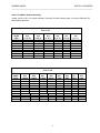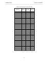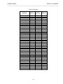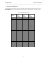
1
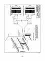
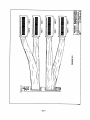
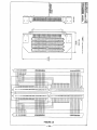
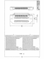
Series 941X/946X
Digital I/O Board
USER’S MANUAL
ACROMAG INCORPORATED
30765 South Wixom Road
P.O. BOX 437
Wixom, MI 48393-7037 U.S.A.
Tel: (248) 624-1541
Fax: (248) 624-9234
8500-244-B97J006
AVME941X/946X
DIGITAL I/O BOARDS
_________________________________________________________________________________
The information in this manual is subject to change without notice. Acromag, Inc., makes no warranty
of any kind with regard to this material, including, but not limited to, the implied warranties of
merchantability and fitness for a particular purpose. Further, Acromag, Inc., assumes no responsibility
for any errors that may appear in this manual and makes no commitment to update, nor keep current,
the information contained in this manual.
No part of this manual may be copied or reproduced in any form, or by any means, without the prior
written consent of Acromag, Inc.
IMPORTANT SAFETY CONSIDERATIONS
It is very important for the user to consider the possible adverse effects of power, wiring, component,
sensor or software failures in designing any type of control or monitoring system. This is especially
important where economic property loss or human life is involved. It is important that the user employ
redundancy, and comprehensive failure analysis to insure a safe and satisfactory overall system
design. It is agreed between the Buyer and Acromag, that this is the Buyer's responsibility.
Acromag, Inc.
30765 South Wixom Road
P.O. Box 437
Wixom, Michigan 48393-7037, USA
Tel: (248) 624-1541
Fax: (248) 624-9234
Copyright 1992, 1995 Acromag, Inc. Printed in USA
Data and specifications subject to change without notice
-1-
AVME941X/946X
DIGITAL I/O BOARDS
_________________________________________________________________________________
TABLE OF CONTENTS
CHAPTER
1.0
1.1
1.2
1.3
1.4
GENERAL INFORMATION......................................................................................................
INTRODUCTION......................................................................................................................
FEATURES OF THE AVME946X.............................................................................................
FEATURES OF THE AVME941X.............................................................................................
VMEbus INTERFACE FEATURES...........................................................................................
Page
4
4
4
4
5
2.0 PREPARATION FOR USE.......................................................................................................
2.1 UNPACKING AND INSPECTION.............................................................................................
2.2 CARD CAGE CONSIDERATIONS...........................................................................................
2.3 BOARD CONFIGURATION......................................................................................................
2.3.1 Default Jumper Configuration...........................................................................................
2.4 ADDRESS ASSIGNMENT........................................................................................................
2.5 JUMPER AND OPTIONS.........................................................................................................
2.6 I/O CONNECTIONS.................................................................................................................
2.7 BACKPLANE REQUIREMENTS..............................................................................................
2.8 USE WITH SOLID STATE RELAYS........................................................................................
2.8.1 Configuring the AVME94XX.............................................................................................
2.8.2 Configuring the PB16A.....................................................................................................
2.9 USE WITH OTHER DEVICES.................................................................................................
2.9.1 Relays and Other Inductive Loads....................................................................................
2.9.2 Contact Closures and Switches........................................................................................
5
5
5
6
6
6
8
8
11
12
12
12
12
12
13
3.0 PROGRAMMING INFORMATION...........................................................................................
3.1 MEMORY MAP.........................................................................................................................
3.1.1 Board Identification PROM...............................................................................................
3.1.2 Board Status Register.......................................................................................................
3.1.3 Digital I/O Port Registers...................................................................................................
3.1.4 Digital Output Register......................................................................................................
13
13
14
15
16
16
4.0
4.1
4.2
4.3
THEORY OF OPERATION.......................................................................................................
VMEbus INTERFACE...............................................................................................................
BOARD CONTROLLER...........................................................................................................
DIGITAL PORT SECTION........................................................................................................
16
16
16
16
5.0
5.1
5.2
5.3
SERVICE AND REPAIR INFORMATION................................................................................
SERVICE AND REPAIR ASSISTANCE...................................................................................
PRELIMINARY SERVICE PROCEDURE................................................................................
PARTS LISTS...........................................................................................................................
17
17
17
17
6.0 SPECIFICATIONS.................................................................................................................... 19
-2-
AVME941X/946X
DIGITAL I/O BOARDS
_________________________________________________________________________________
FIGURES:
2.1
2.2
2.3
2.4
2.5
2.6
2.7
2.8
4.1
4.2
AVME94XX JUMPER LOCATION DRAWING (4500-949).......................................................
9921-16 CONNECTION DIAGRAM (4500-790).......................................................................
9921-32 CONNECTION DIAGRAM (4500-791).......................................................................
AVME946X CONNECTION DIAGRAM (4500-950)..................................................................
9921-16 DIGITAL I/0 ADAPTER CARD (4500-788).................................................................
9921-32 DIGITAL I/0 ADAPTER CARD (4500-789).................................................................
RELAY DRIVER CONFIGURATIONS (4500-743)...................................................................
INPUT CONFIGURATIONS(4500-743)....................................................................................
AVME946X/941X BLOCK DIAGRAM.(4500-948)......................................................................
SIMPLIFIED I/O POINT SCHEMATIC (4500-947)....................................................................
20
21
22
23
24
25
26
26
27
28
AVME946X/941X SCHEMATIC & PART LOCATION DRAWING (4500-946)......................... 29
-3-
AVME941X/946X
DIGITAL I/O BOARDS
_________________________________________________________________________________
1.0 GENERAL INFORMATION
1.1 INTRODUCTION
This manual covers eight models of digitial boards. Table 1.1 lists the model numbers and their major differences.
MODEL
AVME9460
AVME9461
AVME9462
AVME9463
AVME9410
AVME9411
AVME9412
AVME9413
INTERACE
POINTS
64 I/O
64 I/O
32 I/O
32 I/O
64 OUTPUTS
64 OUTPUTS
32 OUTOUTS
32 OUTPUTS
FRONT PANEL
ACCESS
P3, P4, P5, P6
REAR ACCESS
P2
P3, P4
P2
P3, P4, P5, P6
P2
P3, P4
P2
General Features
The AVME946X Digital Input/Output (I/O) Board provides a means for interfacing various discrete devices to a
VMEbus based computer. Interfacing is accomplished by 32 or 64 general purpose I/O points which under
software control may be individually programmed to be inputs or outputs.
1.2 FEATURES OF THE AVME 946X
•
•
•
•
•
•
•
•
•
•
•
32 or 64 programmable I/O points (lines) configured as 4 or 8 - 8 bit ports or 2 or 4 - 16 bit ports all with
inverted logic.
Can read the state of points configured as outputs.
Outputs sink up to 100 mA, from an external 5V supply.
Built in protection diodes for driving relay coils.
Input hysteresis.
Compatible with industry standard solid state relays and termination panels, PB16 and PB32. AVME 9460
and 9462 provide direct connection to the PB16 termination panel, no adapter boards necessary. Optional
universal termination panel available for use with contact closures, relays, incandescent lamps.
TTL and CMOS compatible.
Byte or word data transfers.
Board identification PROM.
Pass/Fail Status indicators on the front panel.
I/O accessible through the front panel or out of the back of the card cage.
1.3 FEATURES OF THE AVME 941X
The AVME941X Digital Output Board provides a means for interfacing various discrete devices to a VMEbus
based computer. Interfacing is accomplished by 32 or 64 output points.
The AVME 941X Digital Output Board features:
•
•
•
32 or 64 programmable Output points (lines) configured as 4 or 8 - 8 bit ports or 2 or 4 - 16 bit ports all with
inverted logic.
Outputs sink up to 100 mA, from up to a 30V external source.
Built in protection diodes for driving relay coils.
-4-
AVME941X/946X
DIGITAL I/O BOARDS
_________________________________________________________________________________
Compatible with industry standard solid state relay termination panels, PB16 and PB32. AVME 9410 and 9412
provide direct connection to the PB16 termination panel, no adapter boards necessary. Optional universal
termination panel available for use with contact closures, relays, incandescent lamps.
•
•
•
•
•
TTL and CMOS compatible.
Byte or word data transfers.
Board identification PROM.
Pass/Fail Status indicators on the front panel.
I/O accessible through the front panel or out of the back of the card cage.
1.4 VMEbus INTERFACE FEATURES
•
•
•
•
•
Slave module A24/A16, D16/D08 (EO).
Short I/O Address Modifiers 29H, 2DH (H = Hex).
Standard Address Modifiers 39H, 3DH (H = Hex).
I(1-7) interrupter, jumper programmable interrupt level, software programmable interrupt vectors (for digital
input channels 0-7), interrupt release mechanism is Release On Register Access (RORA) type.
Decode on 1K byte boundaries.
2.0 PREPARATION FOR USE
This chapter provides information about preparing the Isolated Digital I/O Board for system operation.
2.1 UNPACKING AND INSPECTION
Inspect the shipping carton immediately upon receipt for evidence of mishandling during transit. If the shipping
carton is severely damaged or water stained, request that the carrier's agent be present when the carton is
opened. If the carrier's agent is absent when the carton is opened and the contents of the carton are damaged,
keep the carton and packing material for the agent's inspection.
For repairs to a product damaged in shipment, refer to the Acromag Service Policy to obtain return instructions. It
is suggested that salvageable shipping cartons and packing material be saved for future use in the event the
product must be shipped.
The board is physically protected with foam and electrically protected with an antistatic bag during shipment. It is
advisable to visually inspect the board for evidence of mishandling prior to applying power.
CAUTION
SENSITIVE ELECTRONIC DEVICES
USE ANTI-STATIC HANDLING PROCEDURES
2.2 CARD CAGE CONSIDERATIONS
Refer to the specifications for bus loading and power requirements. Be sure that the system power supplies are
able to accommodate the additional requirements within the voltage tolerances specified.
-5-
AVME941X/946X
DIGITAL I/O BOARDS
_________________________________________________________________________________
Adequate air circulation must be provided to prevent a temperature rise above the maximum operating
temperature. Large and continuing fluctuations in ambient air temperature should be avoided. If the installation is
in an industrial environment and the board is exposed to environmental air, careful consideration should be given
to air filtering.
2.3 BOARD CONFIGURATION
The Digital I/O Board may be configured in a variety of ways for many different applications. Each possible jumper
setting will be discussed in the following sections. The jumper locations are shown in Figure 2.1.
2.3.1 Default Jumper Configuration
VMEBUS INTERFACE CONFIGURATION
When a board is shipped from the factory, it is configured as follows:
•
•
VMEbus Short I/O Address of 0000H.
Set to respond to both Address Modifiers 2DH.
2.4 ADDRESS ASSIGNMENT
Jumpers J17, J18, and J19 are used to establish the base address for the 1k byte block of memory the AVME
94XX will occupy in the Memory Map. J17 and J18 selects the base address. An open, or no jumper installed,
corresponds to a logic 0 state. Refer to Table 2.2 Address Decoding. J19 selects the address modifier codes and
the Standard or Short Memory Map. An open on J19 pins 1 and 2 selects only the Supervisory Access (3DH or
2DH) code. A short on J19 pins 1 and 2 will allow the card to recognize both the Supervisory and the NonPriviledged Access codes. An open, or no jumper installed, on J19 pins 3 and 4 selects Short Memory Map. A
short, or jumper installed, selects Standard Memory Map. Refer to Table 2.1.
Table 2.1 VMEbus Address Modifier Codes
Jumper J19
Address Modifier
Codes Recognized
Pins
3&4
OUT
OUT
Pins
1&2
OUT
IN
2DH
2DH OR 29H
IN
IN
OUT
IN
3DH
3DH OR 39H
-6-
Addressing Mode
Short Supervisory
Short Supervisory or
Short Non-Priveledged
Standard Supervisory
Standard Supervisory or
Standard Non-Priveledged
AVME941X/946X
DIGITAL I/O BOARDS
_________________________________________________________________________________
Table 2.2 VMEbus Address Decoding
Jumper J19 Pins 3 & 4 - No Jumper Installed - Selecting The Short Memory Map. J18 Has No Effect On The
Base Address Selection.
Pins of J17
BASE
ADDR
(HEX)
0000
0400
0800
.
.
.
F400
F800
FC00
S15
(11 & 12)
OUT
OUT
OUT
.
.
.
IN
IN
IN
S14
(10 & 9)
OUT
OUT
OUT
.
.
.
IN
IN
IN
S13
(8 & 7)
OUT
OUT
OUT
.
.
.
IN
IN
IN
S12
(6 & 5)
OUT
OUT
OUT
.
.
.
IN
IN
IN
S11
(4 & 3)
OUT
OUT
IN
.
.
.
OUT
IN
IN
S10
(2 & 1)
OUT
IN
OUT
.
.
.
IN
OUT
IN
Pins of J18
BASE
ADDR
(HEX)
000000
010000
020000
030000
.
.
.
FC0000
FD0000
FE0000
FF0000
S23
(15&16)
OUT
OUT
OUT
OUT
.
.
.
IN
IN
IN
IN
S22
(13&14)
OUT
OUT
OUT
OUT
.
.
.
IN
IN
IN
IN
S21
(11&12)
OUT
OUT
OUT
OUT
.
.
.
IN
IN
IN
IN
S20
(9&10)
OUT
OUT
OUT
OUT
.
.
.
IN
IN
IN
IN
-7-
S19
(7&8)
OUT
OUT
OUT
OUT
.
.
.
IN
IN
IN
IN
S18
(5&6)
OUT
OUT
OUT
OUT
.
.
.
IN
IN
IN
IN
S17
(3&4)
OUT
OUT
IN
IN
.
.
.
OUT
OUT
IN
IN
S16
(1&2)
OUT
IN
OUT
IN
.
.
.
OUT
IN
OUT
IN
AVME941X/946X
DIGITAL I/O BOARDS
_________________________________________________________________________________
2.5 JUMPERS AND OPTIONS
Several jumpers have been included to allow for flexible interfacing to external devices. Table 2.3 describes the
various jumpers and their functions.
TABLE 2.3 Jumper Descriptions
Jumper
Function
Condition as shipped
J2
J4
J6
J10
Port pullup voltage jumper.
When in placem pulls the I/O
lines to +5V through the
removable pullup networks.
Jumpers in place
J9
J7
J5
J15
J3
J13
J1
J11
Port N+0 output driver enable
Port N+1 output driver enable
Port N+2 output driver enable
Port N+3 output driver enable
Port N+4 output driver enable
Port N+5 output driver enable
Port N+6 output driver enable
Port N+7 output driver enable
J1-15 Odd. made with
a thin trace on solder
side. Cutting a jumper
will disable that group of
8 ouputs.
J1 - J15 Odd, are used only in cases where it is absolutely necessary to have outputs disabled through hardware.
See section 3.5, Programming Considerations, for software enabling/disabling of outputs.
2.6
I/O CONNECTIONS
On Model AVME94X1, the 64 I/O points are accessible through a 96 pin Din 41612 connector labeled P2.
CAUTION
DO NOT PLUG P2 INTO ANY BACKPLANES IN A CARD CAGE!
I/O adapter cards (Model 9921-16 or 9921-32) are used to interface between P2 and the ribbon cables. These
adapters mount to the back of a VME cage to provide the mating socket for P2. Refer to termination panel
connection diagrams, figure 2.2 and 2.3.
On Model AVME94X0, four 50-pin ribbon cable connectors (labeled P3, P4, P5 and P6) on the front panel are
used to access the 64 I/O points. Refer to the termination panel connection diagram figure 2.4.
Refer to Table 2.4 for the I/O Connector Pin Assignments.
-8-
AVME941X/946X
DIGITAL I/O BOARDS
_________________________________________________________________________________
Table 2.4 I/O Connectors P2, P3, P4, P5 & P6
Functions
Port N+0 I/O Bit 7
6
5
4
3
2
1
0
Port N+1 I/O Bit 7
6
5
4
3
2
1
0
+5V
GND
GND
Pullup Ports 0 & 1
Protect Ports 0 & 1
Port N+2 I/O Bit 7
6
5
4
3
2
1
0
Port N+3 I/O Bit 7
6
5
4
3
2
1
0
+5V
GND
GND
Pullup Ports 2 & 3
Protect Ports 2 & 3
P2 Pin #
B25
B26
B27
B28
B29
B30
B31
B32
B17
B18
B19
B20
B21
B22
B23
B24
B9
B13,B14
B15,B16
B11
B10
A25
A26
A27
A28
A29
A30
A31
A32
A17
A18
A19
A20
A21
A22
A23
A24
B1
B5,B6
B7,B8
B3
B2
-9-
P3 Pin #
P4 Pin #
33
35
37
39
41
43
45
47
17
19
21
23
25
27
29
31
1,49
2 thru 50
Even
5
3
6
4
33
35
37
39
41
43
45
47
17
19
21
23
25
27
29
31
1,49
2 thru 50
Even
5
3
AVME941X/946X
DIGITAL I/O BOARDS
_________________________________________________________________________________
Table 2.4 Continued
Functions
Port N+4 I/O Bit 7
6
5
4
3
2
1
0
Port N+5 I/O Bit 7
6
5
4
3
2
1
0
+5V
GND
GND
Pullup Ports 4 & 5
Protect Ports 4 & 5
Port N+6 I/O Bit 7
6
5
4
3
2
1
0
Port N+7 I/O Bit 7
6
5
4
3
2
1
0
+5V
GND
GND
Pullup Ports 6 & 7
Protect Ports 6 & 7
P2 Pin #
C25
C26
C27
C28
C29
C30
C31
C32
C17
C18
C19
C20
C21
C22
C23
C24
C9
C15,C16
C13,C14
C11
C10
A8
A7
A6
A5
A4
A3
A2
A1
A16
A15
A14
A13
A12
A11
A10
A9
C1
C5,C6
C7,C8
C3
C2
- 10 -
P5 Pin #
P6 Pin #
33
35
37
39
41
43
45
47
17
19
21
23
25
27
29
31
1,49
2 thru 50
Even
5
3
33
35
37
39
41
43
45
47
17
19
21
23
25
27
29
31
1,49
2 thru 50
Even
5
3
AVME941X/946X
DIGITAL I/O BOARDS
_________________________________________________________________________________
2.7
BACKPLANE REQUIREMENTS
The AVME94XX is electrically and mechanically compatible with the VMEbus Specification Manual, Revision C.
The backplane connection is made through the 96 pin DIN 41612 connector labeled P1. The signals used are
listed in Table 2.5.
Table 2.5 Backplane Connector P1
Pin
Number
1
2
3
4
5
6
7
8
9
10
11
12
13
14
15
16
17
18
19
20
21
22
23
24
25
26
27
28
29
30
31
32
Row A
Signal
Mnemonic
D00
D01
D02
D03
D04
D05
D06
D07
GND
SYSCLK
GND
DS1*
DS0*
WRITE*
GND
DTACK*
GND
AS*
GND
IACK*
Row B
Signal
Mnemonic
AM0
AM1
AM2
AM3
GND
AM4
A07
A06
A05
A04
A03
A02
A01
GND
+5V
+5V
- 11 -
Row C
Signal
Mnemonic
D08
D09
D10
D11
D12
D13
D14
D15
GND
SYSFAIL*
BERR*
SYSRESET*
LWORD*
AM5
A23
A22
A21
A20
A19
A18
A17
A16
A15
A14
A13
A12
A11
A10
A09
A08
+5V
AVME941X/946X
DIGITAL I/O BOARDS
_________________________________________________________________________________
2.8 USE WITH SOLID STATE RELAYS
The AVME 94XX Digital I/O Board may interface with industry standard solid state relays and termination panels
PB16A, PB32 and their equivalents.
2.8.1 Configuring The AVME - 94XX
On the AVME94XX, the following jumpers or shorting clips should be in place: J2, J4, J6 and J10. Pullup resistor
networks R1, R2, R3, R4, R5, R6, R7 and R8 are removable.
Table 2.6 lists the Module Number Bit Positioning for the I/O port registers.
TABLE 2.6 Module Number Bit Positioning
I/O Port
Number
N+0
N+1
N+2
N+3
N+4
N+5
N+6
N+7
Module Number
7 6 5 4 3 2 1 0
7 6 5 4 3 2 1 0
15 14 13 12 11 10 9 8
7 6 5 4 3 2 1 0
15 14 13 12 11 10 9 8
7 6 5 4 3 2 1 0
15 14 13 12 11 10 9 8
7 6 5 4 3 2 1 0
15 14 13 12 11 10 9 8
PB16A connected
to
P3
P3
P4
P4
P5
P5
P6
P6
For bit positions corresponding to output modules, a 1 state will turn the I/O point on and the output latch will sink
current. A 0 state will turn the module off. For bit positions corresponding to input modules, a 1 state indicates the
presence of a low voltage for the "on" state of the module.
A 0 state indicates a high voltage present.
2.8.2 Configuring The PB16A
If the PB16A is to get power from the AVME94XX, install a jumper at pin 1 or pin 49 on the PB16A termination
panel. Install appropriate solid state relay modules. Connect the 50 Pin ribbon cable between PB16A and the
AVME94XX observing the pin 1 index mark.
2.9
USE WITH OTHER DEVICES
The AVME946X/941X Digital Boards can interface with a variety of discrete devices such as relays, switches,
contact closures, and indicators. Optional termination panel 6980-16U can be used to connect field wiring to the
digital I/O card. The following guidelines should be followed to insure proper interfacing.
2.9.1 Relays And Other Inductive Loads
When driving relays coils or other inductive loads, the PROTECT line should be tied to the voltage supply of the
loads. This puts a diode accross each load to limit the voltage spike generated when an inductive load is switched
off quickly. Since PROTECT is common to all 16 outputs, the supply voltage for all of the loads must be the same.
Otherwise, each load will have to have its own external diode. The pullup resistors should be removed from the
digital I/O card also. See figure 2.7 Relay Driver and Input Configurations, for relay driver configurations.
- 12 -
AVME941X/946X
DIGITAL I/O BOARDS
_________________________________________________________________________________
2.9.2 Contact Closures And Switches
When sensing contact closures that already are connected to a voltage source the pullup resistor networks should
be removed. The input voltage should be within the range listed in Specifications, Section 6. For isolated or
grounded contacts the pullups and the +5 volt supply can be used to establish an input voltage. See figure 2.8
Relay Driver and Input Configurations, for various input configurations.
This chapter provides the specific information necessary to program the
Digital I/O Board.
3.0 PROGRAMMING INFORMATION
3.1 The Digital I/O Memory Map
The memory map for the Digital I/O Board, a Non-Intelligent I/O architecture is shown in Figure 3.1. All addresses
are in hexadecimal. The letters R and W indicates whether a register may be read and/or written to. The areas
marked "undefined" in the memory map are reserved for future use. To allow future compatibility, application
programs must not use these areas.
Figure 3.1 AVME94XX Digital I/O Board Memory Map.
Address
Base +
(HEX)
00
↓
3E
40
↓
7E
80
82
↓
FE
100
102
104
106
108
↓
3FE
Even
Odd
R - Module ID PROM
Undefined
Undefined
Undefined
R/W - Status/Control
Undefined
R/W - I/O Port 0
R/W - I/O Port 2
R/W - I/O Port 4
R/W - I/O Port 6
R/W - I/O Port 1
R/W - I/O Port 3
R/W - I/O Port 5
R/W - I/O Port 7
Undefined
Note: For AVME 941X I/O Ports 0-7 are Write Only.
Note: Ports 4 through 7 present only on Models AVME 9410, 9411,9460, 9461.
- 13 -
Address
Base +
(HEX)
01
↓
3f
41
↓
7F
81
83
↓
FF
101
103
105
107
109
↓
3FF
AVME941X/946X
DIGITAL I/O BOARDS
_________________________________________________________________________________
3.1.1 Board Identification PROM (I.D. PROM) - (Read Only)
(01-3F)
The Board Identification PROM occupies the 32 odd bytes beginning at location 01. These bytes contain ASCII
character strings that identify various characteristics of the board. See figure 3.2.
Figure 3.2: Digital Board Identification PROM
Offset
From Board
Base Address
01H
03H
05H
07H
09H
ASCII
Character
V
M
E
I
D
Value
Numeric
Descriptions
56H
4DH
45H
49H
44H
Always VMEID for all boards.
0BH
0DH
0FH
A
C
R
41H
43H
52H
Manufacturers I.D., ACR for ACROMAG.
11H
13H
15H
17H
19H
1BH
1DH
9
4
1
0
39H
34H
31H
30H
20H
20H
20H
Board Model Number ( 7 characters,
blank filled ).
1FH
1
31H
Number of Kilobytes of address
space used.
21H
23H
20H
31H
Major functional revision level.
1
30H
20H
Minor functional revision level.
25H
27H
29H
2BH
2DH
2FH
31H
33H
35H
37H
39H
3BH
3DH
3FH
0
Undefined
Undefined
Undefined
Undefined
Undefined
Undefined
Undefined
Undefined
Undefined
Undefined
Undefined
Undefined
Reserved
- 14 -
AVME941X/946X
DIGITAL I/O BOARDS
_________________________________________________________________________________
3.1.2 Board Status Register - (read/write) - 81H
The Board Status Register reflects and controls functions globally on the board.
MSB
LSB
7
6
5
4
3
2
1
0
---------------------------------------------------------------------------------------------------------------<------ Reserved ------>
Software
<------ Reserved ------> Green
Red
Reset
.
LED
LED
Where:
Bits 7,6,5,3,2: Reserved for future use - equal "0" if read.
Bit 4: Software Reset (W) - writing a "1" to this bit causes a software reset. Writing "0" or reading the bit has no
affect. A software reset turns all of the ports off which effectivly programs the ports for inputs.
Bit 1: Green LED (R/W) - this bit when written will control the state of the green LED on the front panel. A "1" will
turn it on, a "0" will turn it off. Reading it will reflect its current state.
Reset Condition: Will read a "0", LED off.
Bit 0: Red LED (R/W) - this bit when written will control the state of the red LED on the front panel and the state of
the VMEbus SYSFAIL* signal. A "1" will turn it off and set SYSFAIL* high, a "0" will turn it on and set
SYSFAIL* low. Reading it will reflect its current state.
Reset Condition: Will read a "0", LED on, and SYSFAIL* is set low.
The status register bits 1 and 0 along with the green and red LEDs provide the user with a means of keeping track
of a board's functionality in the system. Since there is no intelligence on the board, the host computer controls
these bits. The following is one possible use of the bits in the status register and the LEDs on the front panel.
On power-up the bits in the status register will read low, with the green LED off, the red LED lit, and
SYSFAIL* low. This indicates that the board has failed or that it hasn't been tested yet.
The Status Register Bit 1 reads low and Bit 0 reads high. The LEDs will both be off and SYSFAIL* is high.
This indicates an inactive board.
The Status Register Bit 1 reads high and Bit 0 reads low. The LEDs will both be lit and SYSFAIL* is low.
This indicates the board is undergoing a diagnostic checkout.
The Status Register Bits 1 and 0 read high. The green LED will be lit with the red LED off and SYSFAIL* is
high. This indicates the board is fully functional.
3.1.3 Digital I/O Port Registers - (Read/Write) AVME 946X Only - (100-107)
The I/O Port Registers reflect and/or control the state of the bidirectional I/O points. Points are grouped 8 to a
Port. To use a point as an input, write a "0" to it first to cause the output driver to go into an off (high impedance)
state. That lets the point be pulled to a high voltage level by an onboard pull-up resistor. The point may then be
driven by an external device. Reading the point will reflect the INVERTED level at the I/O connection. To use a
point as an output, write the desired "1" or "0" to the point. If the point is read, it will reflect the state of the output
as well. Note that because inverted logic is used, a high level at the I/O connection is read as a "0" in the Port
Registers and a low level is read as a "1". This is consistant with the usage of open-collector outputs to drive
- 15 -
AVME941X/946X
DIGITAL I/O BOARDS
_________________________________________________________________________________
relays and switches. A logic "1" in the computer produces a low level at the output driver to "pull in" a relay and
turn something "on", etc.
Reset Conditions: All of the I/O points are set to "0" which causes the output drivers to go into an off (hi-z) state.
The result is that all I/O points are configured as inputs.
3.1.4 Digital Output Registers - (Write Only) AVME 941X Only - (100-107)
The Digital Output points are grouped 8 to a port. Writing a "1" to a point causes the open collector output to turn
on, which will bring the output to a low state, sinking current from the output point. Writing a "0" to a point
causes the open collector output to turn off, which will allow the pullup resistors to pull the output point to a high
state.
Reset Conditions: All of the I/O points are in an off (high impedance) state.
4.0 THEORY OF OPERATION
This chapter describes the circuitry of the Digital Board. A block diagram of this board is shown in Figure 4.1.
Schematics of the board are in chapter 7.
4.1 VMEbus Interface
The VMEbus Interface is composed of 3 functional areas:
•
•
•
Data Buffers (U27, U28)
Address Latch, Buffer and Comparators (U21, U3, U22, U24)
Control Buffers (U25, U26)
4.2 Board Controller
The Board Controller is composed of 5 functions: (U19)
•
•
•
•
•
Card and Register decoding
VMEbus Interface controller
PROM controller
Status register
Digital Port controller
4.3 Digital Port Section
The Digital Port is composed of an output latch and an input buffer. A simplified I/O point schematic is shown in
figure 4.2.
-
Output Latch (U1, U3, U5, U7, U9, U11, U13, U15)
Input Buffer (Models AVME 946X only, U2, U4, U6, U8, U10, U12, U14, U16)
- 16 -
AVME941X/946X
DIGITAL I/O BOARDS
_________________________________________________________________________________
5.0 SERVICE AND REPAIR INFORMATION
This chapter provides instructions on how to obtain service and repair assistance, service procedures, and
component parts lists.
5.1 SERVICE AND REPAIR ASSISTANCE
It is highly recommended that a non-functioning board be returned to Acromag for repair. Acromag uses tested
and burned-in parts, and in some cases, parts that have been selected for characteristics beyond that specified by
the manufacturer. Acromag has automated test equipment that thoroughly checks the performance of each
board. When a board is first produced and when any repair is made, it is tested, placed in a burn-in room at
elevated temperature, and retested before shipment.
Please refer to Acromag's Service Policy Bulletin or contact Acromag for complete details on how to obtain parts
and repair.
5.2 PRELIMINARY SERVICE PROCEDURE
Before beginning repair, be sure that all of the procedures in Chapter 2, Preparation For Use, have been followed.
The procedures are necessary since the board has jumpers that must be properly configured.
CAUTION
POWER MUST BE OFF BEFORE REMOVING OR INSERTING BOARDS
Note: It has been observed that on occasion, a "boot" program for a disk operating system will "hang" waiting for
the VMEbus SYSFAIL* signal to be released by an intelligent disk controller board. Acromag's non-intelligent
slave boards assert the SYSFAIL* signal as described in the VMEbus Specification Rev. C.1 and therefore, the
disk operating system will remain "hung". The best solution to this problem is to correct the boot program so that it
is no longer dependent upon the SYSFAIL* signal. When this solution is not practical, it is possible to disconnect
the SYSFAIL* from the circuitry on the Acromag board by cutting a PC board foil near the P1 connector on the
solder side. Caution should be exercised so as not to cut any other foils nor damage the board in any other way.
Call Acromag's Applications Engineering Department for assistance.
5.3 PARTS LISTS
Parts Lists are provided as an aid to the user in troubleshooting the Board (also reference the schematic and part
location drawings. Tables 5.1A to 5.1D list the parts installed on the main board for the various models; similarly
Tables 5.2A to 5.2C list parts for the LED expansion board. Replacement parts and repair services are available
from Acromag.
Changes are sometimes made to improve the product, to facilitate delivery, or to control cost. It is therefore
important to include the Component Reference Number, the Acromag Part Number, the Board Model Number,
and the Board Serial Number when providing information to order parts.
- 17 -
AVME941X/946X
DIGITAL I/O BOARDS
_________________________________________________________________________________
Table 5.1 Replaceable Parts
REFERENCE NO.
ACROMAG PART NUMBER
U1,3,5,7,9,11,13,15
U2,4,6,8,10,12,14,16
U17
U18
U19
U20
U21
U22, 24
U23, 25
U26
U27, 28
R1,2,3,4,5,6,7,8,11
1033-515
1033-272
1033-358
1033-278
1033-715
1033-263
1033-283
1033-626
1033-273
1033-623
1033-627
1100-268
R9,10
C1-C18
C19
C20-C27
D1
D2
D3-D10
F1
P1,P2
P3,P5
1100-490
1002-530
1002-320
1002-315
1001-165
1001-166
1001-168
1030-496
1004-505
1004-592
DESCRIPTION
UCN5801ABU
74LS24OND
2732A-3
74LS257AND
XC2018
74LS32ND
74LS373ND
25LS2521PCB
74LS244ND
74F38N
74LS645-IND
RES NETWORK 9 4700
OHM
RES NETWORK 9 1K
CAP MONO O.1UF
CAP TAN 1 UF
CAP TAN 10UF
LED GREEN
LED RED
DIODE NETWORK
FUSE 2 AMP.
CONN. EDGE 96 MALE RT
CONN. TWO 50 POS
- 18 -
AVME941X/946X
DIGITAL I/O BOARDS
_________________________________________________________________________________
6.0 SPECIFICATIONS
Operating Temperature ...............................................................
Storage Temperature....................................................................
Physical Characteristics:...............................................................
Length......................................................................................
Width........................................................................................
Board Thickness......................................................................
Component Height...................................................................
Recommended Card Spacing..................................................
0 to +70 deg. C
-25 to +85 deg. C
(Double Eurocard)
9.187 in. (233.3 mm)
6.299 in. (160.0 mm)
0.062 in. (1.59 mm)
0.550 in. (13.97 mm)
0.800 in. (20.32 mm)
Mating Connectors:
P1,P2....................................................................................... 96 pin 603-2-IEC class 2
P3,P4....................................................................................... Panduit No. 100-532-033; Type B Male
Connectors, rows A & B equipped,even
pins only (32 pins total).
Power Requirements:
+ 5 Volts (+/-5%)...................................................................... 1.0A typical, 1.5A maximum
+ 12 Volts................................................................................. 0.0mA (no load)
VME BUS LOADING CURRENT................................................. input low
A23 - A10
-0.4 mA
A8 - A1
AS*, IACK*, DS1*, DSO*, WRITE*, ........................................ -0.2 mA
LWORD*, SYSCLK, SYSRESET*
AM5 - AM0, A09
D15 - D0.
-0.1 mA
input high
20 uA
20 uA
20 uA
VME BUS DRIVE CURRENT........................................................ output low
output high
DTACK*, BERR*, SYSFAIL*
D15 - D0
VME BUS ACCESS TIME
-3.0 mA
-15 mA
64 mA
48 mA
<650nS
Measured from the falling edge of DSx* to the falling edge of DTACK*
DIGITAL INPUT/OUTPUT NON-ISOLATED
Input Voltage Range.....................................................................
Input Hysteresis............................................................................
Input Current.................................................................................
Points per Board AVME946X.......................................................
Points per Board AVME941X.......................................................
Output Type..................................................................................
Output Voltage Range AVME946X..............................................
Output Voltage Range AVME941X..............................................
Output Current Sink......................................................................
Output Saturation Voltage - @ 100 mA........................................
Logic Compatability......................................................................
Power Up to Stable Output Time.................................................
Reset to Stable Output Time........................................................
- 19 -
0.0 to 5 V DC
0.4 V DC nominal
0.2 mA nominal
32 or 64; each point can be configured
as an input or an output
32 or 64 outputs
Open collector with removable pull up resistor
0 to 5 V DC
0 to 30 V DC
100 mA max. From an external supply.
24 mA max. From an internal supply.
1.1 V max., 0.9V typ.
TTL, LSTTL, CMOS, and others.
< 500 uS
< 1 uS