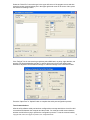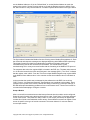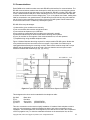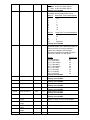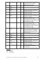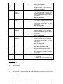
1
D6000 SERIES USERS MANUAL
Version 1.8
Copyright Dutile, Glines, and Higgins Corporation, 2014. All Rights Reserved.
1
Table of Contents:
1.0 Introduction
2.0 Configuration & Getting Started
3.0 Communications
4.0 Module Types
4.1 D6100 Seven Channel Voltage Input Module
4.1.1 Analog to Digital Converter
4.1.2 Pin Assignments and Specifications
4.1.3 Initial Values
4.1.4 Register Assignments
4.1.5 Calibration Procedure
4.2 D6200 Seven Channel Current Input Module
4.2.1 Analog to Digital Converter
4.2.2 Pin Assignments and Specifications
4.2.3 Initial Values
4.2.4 Register Assignments
4.2.5 Calibration Procedure
4.3 D6300 Seven Channel Thermocouple Module
4.3.1 Analog to Digital Converter
4.3.2 Pin Assignments and Specifications
4.3.3 Initial Values
4.3.4 Register Assignments
4.3.5 Calibration Procedure
4.4 D6400 Seven Channel Voltage, Thermocouple, Current Input Module
4.4.1 Analog to Digital Converter
4.4.2 Pin Assignment and Specifications
4.4.3 Initial Values
4.4.4 Register Assignments
4.4.5 Calibration Procedure
4.4.6 D6400 Current Channel Enable
4.5 D6500 Two Channel Analog Output Module
4.5.1 Analog Outputs
4.5.2 Pin Assignments & Specifications
4.5.3 Initial Values
4.5.4 Register Assignments
4.5.5 Voltage Output Calibration Procedure
4.5.6 Current Output Calibration Procedure
4.5.7 Analog Output Calibration Register Tables and Values
4.6 D6710 Fifteen Bit Digital Input Module
4.6.1 Digital Inputs
4.6.2 Pin Assignments
4.6.3 Initial Values
4.6.4 Register Assignments
4.7 D6720 Fifteen Bit Digital Output Module
4.7.1 Digital Outputs
4.7.2 Pin Assignments
4.7.3 Initial Values
4.7.4 Register Assignments
4.7.5 Communications Watchdog Timer
Copyright Dutile, Glines, and Higgins Corporation, 2014. All Rights Reserved.
2
5.0 Modbus Protocol
5.0 Functions
5.1 Function 01 – Read Coil Status
5.2 Function 02 – Read Input Status
5.3 Function 03 – Read Holding Registers
5.4 Function 04 – Read Input Registers
5.5 Function 05 – Force Single Coil
5.6 Function 06 – Preset Single Register
5.7 Function 0F – Force Multiple Coils
5.8 Function 10 – Preset Multiple Registers
6.0 Modbus Exception Error Codes
6.0 D6100 through D6400 Series Modbus Data Values
6.1 Data Registers
6.2 Data Values
7.0 D6000 Series Specifications
Copyright Dutile, Glines, and Higgins Corporation, 2014. All Rights Reserved.
3
WARRANTY
DGH warrants each D6000 series module to be free from defects in materials and workmanship
under normal conditions of use and service and will replace any component found to be defective,
on its return to DGH, transportation charges prepaid within one year of its original purchase. DGH
assumes no liability, expressed or implied, beyond its obligation to replace any component
involved. Such warranty is in lieu of all other warranties expressed or implied.
WARNING
The circuits and software contained in D6000 series modules are proprietary. Purchase of these
products does not transfer any rights or grant any license to the circuits or software used in these
products. Disassembling or decompiling of the software program is explicitly prohibited.
Reproduction of the software program by any means is illegal.
As explained later in this document, all setups are performed entirely from the outside of the
D6000 module. There is no need to open the module because there are no user-serviceable
parts inside. Removing the cover or tampering with, modifying, or repairing by unauthorized
personnel will automatically void the warranty. DGH is not responsible for any consequential
damages.
RETURNS
When returning products for any reason, contact the factory and request a Return Authorization
Number and shipping instructions. Write the Return Authorization Number on the outside of the
shipping box. DGH strongly recommends that you insure the product for value prior to shipping.
Items should not be returned collect as they will not be accepted.
CONTACT INFORMATION
DGH Corporation, USA.
Corporate Offices
Phone: (603) 622-0452
Fax:
(603) 622-0487
Email: [email protected]
SHIPPING ADDRESS
DGH Corporation
Hillhaven Industrial Park
146 Londonderry Turnpike
Hooksett, NH 03106
Attn: RMA#______________
Copyright Dutile, Glines, and Higgins Corporation, 2014. All Rights Reserved.
4
1.0 Introduction
The D6000 series RS-485 serial interface modules are a complete family of data acquisition
modules. The family of modules includes multi-channel analog input measurement modules,
multiple channel analog output modules, and digital modules.
The D6000 series modules communicate using the Modbus RTU protocol. This protocol very
popular in the data acquisition market and is supported by almost every commercial data
acquisition program in the market today. Thus providing access to wide variety of software control
programs that can meet almost any application budget.
The D6000 series analog input modules contain seven differential analog input channels and can
measure voltages, current, and thermocouples. There are four versions available, the D6100,
D6200, D6300 and the D6400. The D6100 module can measure DC voltage signals. The D6200
module can measure seven 4-20mA current loops. The D6300 series can measure eight userselectable thermocouple types. The D6400 series can measure six selectable voltage input
ranges, one current input range, and eight selectable thermocouple types.
The D6500 series analog output modules contain two output channels for generating either a
voltage or current output signal. Each analog output channel is user-selectable as either a voltage
or a current output. These analog output signals can be used as control inputs for items such as
motor controls, valve controls, and other control devices. Each analog output channel also
contains a programmable communications watchdog timer for instances when communications to
the module is lost.
The D6700 series digital input and output modules each contain 15-bits of input or output. The
digital input modules contain internal pull-ups on each bit for direct connection of dry contact
switches. The digital outputs are open-collector outputs that can be connected up to 30Vdc and
can sink 100mA per bit. The open-collector allows the modules to be used in a wider variety of
control applications. The digital output module also contains a programmable watchdog timer for
instances where communications to the module is lost.
Mixing and matching the D6000 series modules together in an application provides a user with all
the measurement and control hardware for a complete process control system.
Copyright Dutile, Glines, and Higgins Corporation, 2014. All Rights Reserved.
5
2.0 Configuration & Getting Started
Default Mode
All D6000 series modules contain an EEPROM (Electrically Erasable Programmable Read Only
Memory) to store setup information and calibration constants. The EEPROM replaces the usual
array of switches and pots necessary to specify baud rate, address, parity, etc. The memory is
nonvolatile which means that the information is retained even if power is removed. No batteries
are used so it is never necessary to open the module case.
The EEPROM provides tremendous system flexibility since all of the module’s setup parameters
may be configured remotely through the communications port without having to physically change
switch and pot settings. There is one minor drawback in using EEPROM instead of switches;
there is no visual indication of the setup information in the module. It is impossible to tell just by
looking at the module what the baud rate, address, parity and other settings are. It is difficult to
establish communications with a module whose address and baud rate are unknown. To
overcome this, each module has an input pin labeled DEFAULT*. By connecting this pin to
Ground, the module is put in a known communications setup called Default Mode.
The Default Mode settings are: 9600 baud, one start bit, eight data bits, one stop bit, no parity,
any address is recognized. The module will answer to address “01” in the Default Mode.
Grounding the DEFAULT* pin does not change any of the setups stored in EEPROM. The setup
information may be read back to determine all of the setups stored in the module.
Setup information in a module may be changed at will in the Default Mode. The baud rate and
parity setups may be changed without affecting the Default Mode values of 9600 baud and no
parity. When the DEFAULT* pin is released, the module automatically performs an internal reset
and configures itself to the baud rate and parity stored in the setup information.
The Default Mode should only be used with a single module connected to a computer for the
purpose of identifying and modifying setup values. In most cases, a module in Default Mode may
not be used in a string with other modules.
Communications Connections
The D6000 series module must be connected to a host computer with an RS-485 serial port for
configuration. For computers that contain an internal RS-232 port then the DGH A1000 RS-232 to
RS-485 serial converter can be used to connect the module to a computer. For computers without
internal serial ports then a DGH USB-COMi USB to RS-485 converter can be used to connect the
module to a computer. The RS-485 serial connections for both devices are detailed below.
A1000 RS-485 Connections
A1000 RS-485 Out Connector
(B) GND
(R) +VS
(G) DATA(Y) DATA+
D6000 Module Connector
GND
+VS
DATADATA+
USB-COMi RS-485 Connections
USB-COMi DB-9 Connector
Pin 5
Pin 1
Pin 2
D6000 Module Connector
GND
DATADATA+
Note: When using the USB-COMi a separate power supply will be required
and connected between the +VS and GND terminals.
Copyright Dutile, Glines, and Higgins Corporation, 2014. All Rights Reserved.
6
DEFAULT Mode Connection
For simplicity, we recommend performing all the setups while in the Default Mode. Place the
D6000 in Default Mode by connecting the DEFAULT* terminal to the GND terminal using a
jumper wire. When the module is in the Default Mode the serial parameters are internally set to:
9600 Baud, 8 data bits, no parity and one stop bit. The module will respond to Modbus Slave
address “01”.
Note: No other wiring connections are required on the analog or digital I/O pins to perform the
module configuration.
1.1 Getting Started
The first step towards “Getting Started” with your D6000 series module is to connect the module
to an RS-485 serial port using the wiring connections above. Included within the wiring
connections is the “Default*” line being connected to the power supply ground. This connection
places the module in the “Default Mode”. The Default Mode forces the module into a known
communications state and is best utilized for configuring the module. The Default Mode serial
communications parameters are: 9600 baud, eight data bits, no parity and one stop bit. The
module will answer to Modbus Slave address “1” (0x01).
The D6000 series modules require a software program to change the setup register values. Since
the modules communicate via the Modbus RTU protocol, a Modbus Master program or the DGH
D6000 series Utility Software will be required to change the module configuration.
The DGH D6000 Series Utility Software is the best program to use when configuring a module.
The utility software reads the module information, displays the information in easy to understand
terms, allows changes to be made via drop-down list boxes and then writes the new values back
to the module. The module parameters can also be stored to disk and recalled at a later date.
The D6000 series Utility Software is provided free of charge on CDROM with a purchase order
and the latest version is always downloadable from www.dghcorp.com. The utility software runs
on Windows based computers. Simply insert the CDROM into the CDROM drive, or download the
Setup.Exe file from the website, and then run the SETUP.EXE installation file. The software will
install and create a menu section called “DGH DATA ACQUISITION” and the Utility Software will
be under that selection.
From the computer desktop select the “start” button, select “all programs”, select “DGH Data
Acquisition” and then select “D6000 Series Utility Software” to run the utility software. When the
software opens the first step is to select, configure and open the host serial communications port
where the module is connected.
Copyright Dutile, Glines, and Higgins Corporation, 2014. All Rights Reserved.
7
Select the “Serial Port” connection type in the upper left corner of the program screen and then
select the proper communications port in the upper right hand corner of the screen. Next, press
the Serial Port “Settings” button.
If the “Default*” line is connected to ground then select 9600 baud, no parity, eight data bits, one
stop bit, RTS Only handshaking and the Tx and Rx delays can be left in their default state.
Otherwise, adjust the communications settings to match the settings in the connected module.
Press the “Open Port” or “Update” button to complete the serial port configuration process.
Test Communications
After the utility software serial port has been configured the next step would be to check for valid
communications between the computer and the module. You must have valid communications
with the module before trying to perform the configuration process. To test the communications,
Copyright Dutile, Glines, and Higgins Corporation, 2014. All Rights Reserved.
8
set the Modbus Address to 01 in the “Default Mode” or set the Modbus Address to match the
setting in the module. Set the Function selector to 03 and the Register selector to 40001. Press
the “Send” button to verify communications. A module response will be shown in the figure below.
The figure above illustrates the Modbus function 03 being sent to Modbus Slave address 01. Both
the command and response messages are displayed beginning with CMD and RSP respectively.
This display format is provided for troubleshooting purposes as it displays each byte of
information being sent to and received from the module. This format can be a good
troubleshooting tool or a way to become familiar with the formatting of the Modbus RTU protocol.
The response data value from register 40001 is located in the RSP: line. The data value returned
is a 16-bit value located in the fourth and fifth bytes in the message (00 01). The “00 01” indicates
that the register value is 0001. From the 7CH Current Input Modbus Register map, register 40001
is the Modbus Slave address value. In the case the module slave address value is read back as
0001.
In the event that the module was not detected by the software then the RSP: line would say
“RSP: Timeout – No Response Detected!”. Several things can contribute to this problem. Some
examples are no power to the module, bad RS-485 wiring connection(s), invalid port settings, or
RS-485 half-duplex handshaking problems all can cause timeout errors. Timeout errors must be
corrected before attempting to configure a module.
Setup a Module
After a successful communications test has been performed then the module can be configured.
Select the type of module using the drop-down list box under “Quick Setup” in the lower left hand
corner of the screen. Then press the “Setup” button. A new screen (see below) will appear that
contains list of all the user-selectable module values. Several different screens can appear. Each
screen is specific to the type of module connected. The screen below is for a seven channel
current input module.
Copyright Dutile, Glines, and Higgins Corporation, 2014. All Rights Reserved.
9
Ensure that the Module Address in the lower left corner is 01 and then press the “Read Setup”
button. The screen will now populate with the existing configuration data inside the module.
The user-selectable values will be displayed in an easy to understand format and new selections
can be made using the drop-down list boxes. The drop-down list boxes make the configuration
process easy and accurate because erroneous values cannot be entered.
Once the new module configuration settings have been changed to meet the application
requirements then press the “Apply” button to transmit the new settings.
Copyright Dutile, Glines, and Higgins Corporation, 2014. All Rights Reserved.
10
Scan Module Data Values
After the module has been properly configured, the analog input module configuration screens
can poll modules in order to verify the data from each channel. This feature is a good
troubleshooting or verification tool when the analog input signals are physically connected to the
module.
The analog input screens contain a “Scan” button that will start the scanning process. Each data
channel is read by requesting the data values from data registers within the module. The analog
input data registers can be found in the Modbus Register map and the data register locations are
specific to the module type.
The data values are returned in hexadecimal percentage of Full Scale format where a value of
0x0000 represents the minus full scale input of the module. A value of 0xffff represents the
positive full scale input of the module. These values can be used as check to ensure that the
channels are operating properly when analog input signals are applied to the input terminals.
The data values can also be displayed as a numerical value. The utility software knows the plus
and minus full scale input limits for each channel. Using the raw hexadecimal percentage of full
scale data values the software can convert these readings to millivolts, milliamps, or temperature
readings. Simply uncheck the “Display Hex Values” selection underneath the channel readings to
display the numeric values.
The scanning process will also log and display the highest (peak) and lowest (valley) readings
that were recorded during the scanning process. This is just for indication purposes only.
A scan interval slide control is also provided to speed up or slow down the scanning process. This
slide control allows the channels to be scanned at intervals from 0.5 to 5 seconds.
Copyright Dutile, Glines, and Higgins Corporation, 2014. All Rights Reserved.
11
3.0 Communications
Each D6000 series module contains a two-wire RS-485 serial interface for communications. The
RS-485 communications standard was developed to satisfy the need for multi-dropped systems
that can communicate at high data rates over long distances. RS-485 is similar to RS-422 in that
it uses a balanced differential pair of wires switching from 0 to 5V to communicate data. RS-485
receivers can handle common mode voltages from -7V to +12V without loss of data, making them
ideal for transmission over great distances. RS-485 differs from RS-422 by using one balanced
pair of wires for both transmitting and receiving. Since an RS-485 system cannot transmit and
receive at the same time it is inherently a half-duplex system.
RS-485 offers many advantages:
1) balanced line gives excellent noise immunity
2) can communicate with modules at high baud rates
3) communicate at distances up to 4,000 feet.
4) true multi-drop configuration as the modules are connected in parallel
5) individual modules may be disconnected without affecting other modules
6) up to 32 modules on one segment of the communications line; 247 with repeaters
7) simplified wiring using standard telephone cable
Figure 2.0 below illustrates the wiring required for multiple-module RS-485 system. Notice that
every module has a direct connection to the host system. Any number of modules may be
unplugged without affecting the remaining modules. Each module must be setup with a unique
address and the addresses can be in any order. Also note that the connector pins on each
module are labeled with notations (B), (R), (G), and (Y).
Figure 2.0 Typical RS-485 Serial Communications System Architecture
This designates the colors used on standard 4-wire telephone cable:
(B) GND
(R) V+
(G) DATA*
(Y) DATA
Black Wire
Red Wire
Green Wire
Yellow Wire
(RS-485 DATA-)
(RS-485 DATA+)
This color convention can be used to simplify installation. If standard 4-wire telephone cable is
used, it is only necessary to match the labeled pins with the wire color to guarantee correct
installation. The RS-845 data lines are designated on the label as DATA* and is the complement
of DATA (negative true). To minimize unwanted reflections on the transmission line, the bus
Copyright Dutile, Glines, and Higgins Corporation, 2014. All Rights Reserved.
12
should be arranged as a line going from one module to the next. ‘Tree’ or random structures of
the transmission line should be avoided. For wire runs greater than 500 feet, each end of the line
should be terminated with a 220 ohm resistor connected between DATA and DATA*.
When using a bi-directional RS-485 system, there are unavoidable periods of time when all
stations on the line are in receive mode. During this time, the communications lines are left
floating and are very susceptible to noise. To prevent the generation of random characters, the
lines should be biased in a MARK condition as shown in Figure 2.0. The 1K resistors are used to
keep the DATA line more positive than the DATA* line when none of the RS-485 communications
transmitters are on.
When enabled, the low impedance of an RS-485 driver easily overcomes the load presented by
the resistors. Special care must be taken with very long busses (greater than 1000 feet) to ensure
error-free operation. Long busses must be terminated as described above. The use of twisted
cable for the DATA and DATA* lines will greatly enhance signal fidelity.
In situations where many modules are used on a long line, voltage drops in the power leads
becomes an important consideration. The GND wire is used both as a power connection and the
common reference for the transmission line receivers in the modules. Voltage drops in the GND
leads appear as a common-mode voltage to the receivers. The receivers are rated for a
maximum of -7Vdc of common-mode voltage. For reliable operation, the common mode voltage
should be kept below -5V. To avoid problems with voltage drops, modules may be powered
locally rather than transmitting the power from the host.
Inexpensive ‘calculator’ type power supplies are useful in remote locations. When local supplies
are used, be sure to provide a ground reference with a third wire to the host or through a good
earth ground. With local supplies and an earth ground, only two wires for the data connections
are necessary.
Copyright Dutile, Glines, and Higgins Corporation, 2014. All Rights Reserved.
13
4.0 Module Types
The D6000 series RS-485 serial interface modules are a complete family of data acquisition
modules. Mixing and matching the D6000 series modules together in an application provides a
user with all the measurement and control hardware to build a complete process control system.
The family of modules includes multi-channel analog input measurement modules, multiple
channel analog output modules, and digital modules.
D6100 Voltage Input Module
The D6100 series analog input modules contain seven differential inputs for measuring DC
voltages. Each input can be individually configured to measure one of six different voltage
ranges. The input ranges are: +/-0.025V, +/-0.05V, +/-0.10V, +/-1V, +/-5V and +/-10V.
D6200 Current Input Module
The D6200 series analog input module contains seven differential inputs for measuring current
signals such as 4-20mA loops. The analog input range is factory configured for +/-20mA.
D6300 Thermocouple Input Module
The D6300 series analog input module contains seven differential inputs for measuring
thermocouple probes. Each input can be individually configured to measure one of eight different
thermocouple types. The supported thermocouple types are: J, K, T, E, R, S, B and C.
D6400 Voltage, Thermocouple and Current Input Module
The D6400 series analog input module contains seven differential inputs for measuring DC
voltages, thermocouples and current. Each input can be individually configured to measure one of
fourteen different ranges. The supported thermocouple types are: J, K, T, E, R, S, B and C. The
DC voltage input ranges are: +/-0.025V, +/-0.05V, +/-0.10V, +/-1V, +/-5V and +/-10V and the
current input range is +/-20mA.
D6500 Analog Output Module
The D6500 series analog output modules contain two analog output channels for generating
either a voltage or current output signal. Each analog output channel contains two user-selectable
voltage output ranges and two current output ranges. These analog output signals can be used
as control inputs for items such as motor controls, valve controls, and other control devices. Each
analog output channel also contains a programmable communications watchdog timer for
instances when communications to the module is lost.
D6700 Digital Inputs/Output Module
The D6710 modules each contain 15-bits of digital inputs and contains internal pull-ups on each
bit for direct connection to dry contact switches.
The D6720 digital output modules contain fifteen open-collector outputs that can be connected up
to 30Vdc and can sink 100mA per bit. The open-collector outputs allow the modules to be used in
a wide variety of control applications. The digital output module also contains a programmable
communications watchdog timer for accidental instances where communication to the module is
lost.
Copyright Dutile, Glines, and Higgins Corporation, 2014. All Rights Reserved.
14
4.1 D6100 - Seven Channel Voltage Input Module
Overview
The D6100 series analog input modules contain seven differential analog inputs that can
measure six different DC voltage ranges. Each analog input channel is user programmable and
may be assigned to measure a different range. Any unused channels can be disabled.
4.1.1 Analog to Digital Converter
The D6100 series analog input modules contain a 16-bit analog to digital converter to perform the
signal conversion to digital information. The analog to digital converter performs a total of 25
conversions per second. Meaning, if all 7 channels were enabled the each channel would be
measured 3+ times per second. The conversion rate per channel can be improved by disabling
any unused channels.
Features and Register Assignments
The D6100 series analog input modules contain many user-selectable features. The user can
select all features such as baud rate, parity type, analog range selection and digital filtering. The
complete list of features is illustrated in the “Seven Analog Voltage Input Register Assignments”
register map below. The register map format is used for consistency with the Modbus RTU
protocol. The register map contains the register numbers in decimal format, register description,
acceptable data values, and list of what each value means. These registers can be written to
using most any Modbus master program or using the DGH D6000 series utility software.
Note: All Modbus Register values in the tables below are represented as “decimal” numbers.
Analog Data Values
The D6100 series analog input modules contain seven analog channels and the data values are
each stored in registers to be read by the Modbus RTU protocol. The analog data values can be
read using either Function 03 or Function 04. For discussion purposes - we will use the Function
03 register values when referring to the location of the analog data values. The first analog input
data register is located at register 40049 and there are seven consecutive registers
(40049..40055) that contain data values. See Chapter #6 for analog data scaling examples.
Factory Initial Values
The D6100 series analog module features are initialized at the factory with a set of “Initial
Values”. A complete list of factory “Initial Values” can be found in the table below. For reference
purposes, the Modbus Slave address is preset to hex 0x01, the baud rate is 9600, Parity type is
None and the Stop Bits is “1”.
Calibration
The D6100 series analog input modules are shipped from the factory as fully calibrated devices.
Throughout the lifetime of the module there may be need to verify or adjust the calibration of the
device. The verification and adjustment process should only be completed using NIST traceable
calibration equipment. A D6100 series Calibration procedure is included below.
Connector Pin Designations
The D6100 series module uses two 3.81mm removable plugs for connecting signals to the
module. One six-pin connector is for the power supply and the host RS-485 data line
connections. A second sixteen-pin connector is used to connect analog input signals to the
module. The pin designations for each connector are printed on the module label and are listed in
a table below.
Copyright Dutile, Glines, and Higgins Corporation, 2014. All Rights Reserved.
15
4.1.2 D6100 Pin Assignments and Specifications
Connections
Specifications
Power & Serial Communications
Pin Number
1
2
3
4
5
6
Pin
GND
+VS
DataData+
Default*
GND
Designator
- Power Supply
+ Power Supply
RS-485 DataRS-485 Data+
Default*
- Power Supply
Analog Input Pin Assignments
Pin Number
1
2
3
4
5
6
7
8
9
10
11
12
13
14
15
16
Pin
CH1+
CH1CH2+
CH2CH3+
CH3CH4+
CH4CH5+
CH5CH6+
CH6CH7+
CH7ISO. GND
ISO. GND
Designator
CH1 +Input
CH1 -Input
CH2 +Input
CH2 -Input
CH3 +Input
CH3 -Input
CH4 +Input
CH4 -Input
CH5 +Input
CH5 -Input
CH6 +Input
CH6 -Input
CH7 +Input
CH7 -Input
Isolated GND
Isolated GND
Analog Inputs
7 Channels
User Selectable Input Ranges
Bipolar Voltage
10V, 5V, 1V,
0.1V, 0.05V,
0.025V
Differential Reading
CH to CH
Protocol
Serial
Modbus RTU
Power Supply
Voltage
Power
+10-30Vdc
1.4W
Connectors
Spacing
Max Wire Size
Max Current
3.81mm
14-24 AWG
8 Amperes
Serial LED Displays
Transmit (Top)
Receive (Bottom)
Serial TxData
Serial RxData
Copyright Dutile, Glines, and Higgins Corporation, 2014. All Rights Reserved.
16
4.1.3 D6100 Initial Values
Module Parameter
Slave Address
Baud Rate
Parity Type
Modbus Response Delay
Modbus Query Delay
Conversion Rate
Large Signal Filter
Small Signal Filter
Channel 0 Range
Channel 1 Range
Channel 2 Range
Channel 3 Range
Channel 4 Range
Channel 5 Range
Channel 6 Range
Value
1
9600
None
3mS
0mS
60Hz
0 Seconds
0 Seconds
+/-10Vdc
+/-10Vdc
+/-10Vdc
+/-10Vdc
+/-10Vdc
+/-10Vdc
+/-10Vdc
Copyright Dutile, Glines, and Higgins Corporation, 2014. All Rights Reserved.
17
4.1.4 D6100 Register Assignments
Register
40001
40002
40003
Description
Slave Address
UART Setup
Modbus Delays
Function
R/W
R/W
R/W
Value
1-DF
0-303F
40033
40048
Software Version
Last Converted
Chan,
Conversion
Counter
R
R
0-06FF
40049
40050
40051
40052
40053
40054
40055
Channel 0 Data
Channel 1 Data
Channel 2 Data
Channel 3 Data
Channel 4 Data
Channel 5 Data
Channel 6 Data
R
R
R
R
R
R
R
0-FFFF
0-FFFF
0-FFFF
0-FFFF
0-FFFF
0-FFFF
0-FFFF
Description
Factory set to 0x0001.
Bits 0-4 Baud Rate
5=9600
6=19.2K
7=38.4K
8=57.6K
9=115.2K
Bits 5-6 Parity
0=No Parity, 8-N-2
1=Odd
2=Even
3=No Parity, 8-N-1
Factory set to 0x0035 = 9600, 8, N, 1.
Bits 0-7
The Response Delay in milliseconds. This is
required when the RS-485 adapter cannot
tri-state immediately after the last character
is transmitted from the host. Maximum value
is 63mS. Factory default value is 3.
Bits 8-15
The End of Query Delay in milliseconds
(48mS max). This is an additional time that
the module will wait prior to marking the end
of the message. Slower host computers may
not be able transmit a continuous message
stream, thereby creating gaps between
characters exceeding the normal 3.5
character times limit. Factory default value is
0.
Factory set, 0x0003.
Factory set, Code Version.
Bits 0-7
The counter increments each conversion and
rolled over after FF. The Conversion Counter
indicates when the data registers have been
updated.
Bits 8-10
Input channel last conversion stored. The
information is useful when all channel data is
read back with 1 query. The user can identify
which channels have been converted since
the last query as long as the time between
queries is less than 8 conversion times.
Initialized to ‘0x0000’ on device reset.
Data - Ch 0, Offset binary, zero=0x8000.
Data - Channel 1
Data - Channel 2
Data - Channel 3
Data - Channel 4
Data - Channel 5
Data - Channel 6
Copyright Dutile, Glines, and Higgins Corporation, 2014. All Rights Reserved.
18
40095
Misc. Setup
R/W
0-1
40096
Signal Filtering
R/W
0-3F
40097
Setup Channel 0
R/W
0-F
Bit 0 – Normal Mode Rejection Setting
0 – 60Hz, 25 Hz Conversion Speed.
1 – 50Hz, 20 Hz Conversion Speed.
Factory set to 0x0000.
This register controls all channels. Time
constants are only approximate values.
Bits 0-3 Small Filter Time Constant(Secs)
0
0
1
0.5
2
1
3
2
4
4
5
8
6
16
7
32
Bits 4-7
Large Filter Time Constant(Secs)
0
0
1
0.5
2
1
3
2
4-7
Reserved
Factory set to 0x0000.
Channel 0 range. Non-volatile write
protected register. If the EEPROM cannot be
written because of not being enabled, it
replies with a Negative Acknowledge
Exception response 07h. Modbus function
code 10h is limited to 4 data values.
40098
Setup Channel 1
R/W
0-F
40099
Setup Channel 2
R/W
0-F
40100
Setup Channel 3
R/W
0-F
40101
Setup Channel 4
R/W
0-F
40102
Setup Channel 5
R/W
0-F
40103
Setup Channel 6
R/W
0-F
40114
Trim Zero, 10V
Range
WP
0
40115
Trim Zero, 5V
Range
Trim Zero, 1V
Range
Trim Zero, 0.1V
WP
0
Range:
Bits 0-7 Hex
Disable Channel
00
+/-10V
01
+/-5V
02
+/-1V
03
+/-0.100V
04
+/-0.050V
05
+/-0.025V
06
Factory set to 0x0001.
Holds Channel 1 range.
Factory set to 0x0001.
Holds Channel 2 range.
Factory set to 0x0001.
Holds Channel 3 range.
Factory set to 0x0001.
Holds Channel 4 range.
Factory set to 0x0001.
Holds Channel 5 range.
Factory set to 0x0001.
Holds Channel 6 range.
Factory set to 0x0001.
Forces all Channel Data Registers to 8000h,
with input signal equal to zero. Apply
calibration signal at least 15 seconds prior to
calibrating to all channels. Calibration
Acknowledge Exception Response.
Calibration takes 20 seconds.
Refer to Modbus register 40114.
WP
0
Refer to Modbus register 40114.
WP
0
Refer to Modbus register 40114. Apply
40116
40117
Copyright Dutile, Glines, and Higgins Corporation, 2014. All Rights Reserved.
19
Range
40118
Trim Zero, 0.05V
Range
WP
0
40119
Trim Zero,
0.025V Range
WP
0
40146
Trim FS, 10V
Range
WP
D000FFFE
40147
Trim FS, 5V
Range
Trim FS, 1V
Range
Trim FS, 0.1V
Range
WP
D000FFFE
D000FFFE
D000FFFE
40150
Trim FS, 0.05V
Range
WP
D000FFFE
40151
Trim FS, 0.025V
Range
WP
D000FFFE
40241
Control Register
W
40148
40149
WP
WP
calibration signal at least 1 minute prior to
calibrating to all channels.
Refer to Modbus register 40114. Apply
calibration signal at least 1 minute prior to
calibrating to all channels.
Refer to Modbus register 40114. Apply
calibration signal at least 1 minute prior to
calibrating to all channels.
Forces all Channel Data Registers to written
value, with appropriate input signal. Apply
calibration signal at least 15 seconds prior to
calibrating to all channels. Acknowledge
Exception Response. Calibration takes 20
seconds. See note 1.
See Modbus Register 40146.
See Modbus Register 40146.
See Modbus Register 40146. Apply
calibration signal at least 1 minute prior to
calibrating to all channels.
See Modbus Register 40146. Apply
calibration signal at least 1 minute prior to
calibrating to all channels.
See Modbus Register 40146. Apply
calibration signal at least 1 minute prior to
calibrating to all channels.
0 – Normal operation (NOP)
1 – Remote Reset (write protected)
2 – Write Enable
5 – Initialize Host Communication setup
Functions:
R
Read Only
R/W
Read/Write
WP
Write-Protected
Copyright Dutile, Glines, and Higgins Corporation, 2014. All Rights Reserved.
20
4.1.5 D6100 Calibration Procedure
Required Equipment:
1. Computer running the DGH Utility Software or another Modbus Master program.
2. A NIST traceable DC Voltage Standard with +/-10Vdc range.
Setup Steps – Perform Calibration Steps in Order Listed:
1.
2.
3.
4.
5.
6.
Allow unit to warm up for 15 minutes.
Short all the +Input pins together using short jumper wires.
Short all the -Input pins together using short jumper wires.
Connect the +Input wires to the Positive terminal on the DC voltage calibrator.
Connect the -Input wires to the Negative terminal on the DC voltage calibrator.
Install the DGH Utility Software or another Modbus Master Program to communicate with,
and calibrate with the module via serial port or a TCP/IP connection.
Trim Zero:
1. Set the DC calibrator voltage output to +0.0000Vdc.
2. Use the DGH Utility Software or a Modbus Master program to perform steps #3 & #5.
3. Set all channels to the same range. Start with +/-10Vdc range, work downward as per
values in Table 1.0.
4. Trim Zero on all channels.
a. Write a value of 0x0002h to Control Register 40241 to Write-Enable the module.
b. Retrieve Trim Zero register value for specific range from Table 2.0 below.
c. Write value of 0x00h to Range Trim Zero register, (ie. 40114 for +/-10V).
d. Perform steps #4a through #4c to trim zero on each range.
Trim Span:
1. Set the DC calibrator voltage output to +10.000Vdc.
2. Use the DGH Utility Software or a Modbus Master program to perform steps #3 & #5.
3. Set all channels to the same range. Start with +/-0.025Vdc range, work upward as per
values in Table 3.0.
4. Trim Span on each channel.
a. Write a value of 0x0002h to Control Register 40241 to Write-Enable the module.
b. Retrieve Trim Span register value for specific range from Table 2.0 below.
c. Write value of 0xfffe to Trim Span register, (ie. 40146 for +/-10V).
d. Perform steps #4a through #4c to trim span on each range.
Copyright Dutile, Glines, and Higgins Corporation, 2014. All Rights Reserved.
21
4.1.6 D6100 Calibration Tables:
Seven Channel Range Register Values
Channel
Range Control
Channel 0
40097
Channel 1
40098
Channel 2
40099
Channel 3
40100
Channel 4
40101
Channel 5
40102
Channel 6
40103
Table 1.0 Register Setup Values.
00
01
02
03
04
05
06
Range Values
Disabled
+/-10V
+/-5V
+/-1V
+/-0.1V
+/-0.05V
+/-0.025V
Trim Zero Registers and Calibration Values
Range
Register
+/-10Vdc
40114
+/-5Vdc
40115
+/-1Vdc
40116
+/-0.1Vdc
40117
+/-0.05Vdc
40118
+/-0.025Vdc
40119
Table 2.0 Trim Zero Registers and Values.
Value
0000
0000
0000
0000
0000
0000
Trim Span Registers and Calibration Values
Range
Register
+/-0.025Vdc
40151
+/-0.05Vdc
40150
+/-0.1Vdc
40149
+/-1Vdc
40148
+/-5Vdc
40147
+/-10Vdc
40146
Table 3.0 Trim Span Registers and Values.
Value
FFFE
FFFE
FFFE
FFFE
FFFE
FFFE
Copyright Dutile, Glines, and Higgins Corporation, 2014. All Rights Reserved.
22
4.2 D6200 - Seven Channel Current Input Module
Overview
The D6200 series analog input module contains seven differential analog inputs for measuring
current signals such as 4-20mA loops. Each analog input channel can measure current signals
up to +/-20mA. Any unused channels can be disabled.
4.2.1 Analog to Digital Converter
The D6200 series analog input modules contain a 16-bit analog to digital converter to perform the
signal conversion to digital information. The analog to digital converter performs a total of 25
conversions per second. Meaning, if all 7 channels were enabled the each channel would be
measured 3+ times per second. The conversion rate per channel can be improved by disabling
any unused channels.
Features and Register Assignments
The D6200 series analog input modules contain many user-selectable features. The user can
select all features such as baud rate, parity type, analog range selection and digital filtering. The
complete list of features is illustrated in the “Seven Channel Analog Current Input Register
Assignments” register map below. The register map format is used for consistency with the
Modbus RTU protocol. The register map contains the register numbers in decimal format, register
description, acceptable data values, and list of what each value means. These registers can be
written to using most any Modbus master program or using the DGH D6000 series utility
software.
Note: All Modbus Register values in the tables below are represented as “decimal” numbers.
Analog Data Values
The D6200 series analog input modules contain seven analog channels and the data values are
each stored in registers to be read by the Modbus RTU protocol. The analog data values can be
read using either Function 03 or Function 04. For discussion purposes - we will use the Function
03 register values when referring to the location of the analog data values. The first analog input
data register is located at register 40049 and there are seven consecutive registers
(40049..40055) that contain data values. See Chapter #6 for analog data scaling examples.
Factory Initial Values
The D6200 series analog module features are initialized at the factory with a set of “Initial
Values”. A complete list of factory “Initial Values” can be found in the table below. For reference
purposes, the Modbus Slave address is preset to hex 0x01, the baud rate is 9600, Parity type is
None and the Stop Bits is “1”.
Calibration
The D6200 series analog input modules are shipped from the factory as fully calibrated devices.
Throughout the lifetime of the module there may be need to verify or adjust the calibration of the
device. The verification and adjustment process should only be completed using NIST traceable
calibration equipment. A D6200 series Calibration procedure is included below.
Connector Pin Designations
The D6200 series module uses two 3.81mm removable plugs for connecting signals to the
module. One six-pin connector is for the power supply and the host RS-485 data line
connections. A second sixteen-pin connector is used to connect analog input signals to the
module. The pin designations for each connector are printed on the module label and are listed in
a table below.
Copyright Dutile, Glines, and Higgins Corporation, 2014. All Rights Reserved.
23
4.2.2 D6200 Pin Assignments and Specifications
Connections
Specifications
Power & Serial Communications
Pin Number
1
2
3
4
5
6
Pin
GND
+VS
DATADATA+
Default*
GND
Designator
- Power Supply
+ Power Supply
RS-485 DataRS-485 Data+
Default*
- Power Supply
Analog Inputs
7 Channels
Input Range
Current
+/-20mA
Differential Reading
CH to CH
+/-10Vdc
Protocol
Serial
Modbus RTU
Power Supply
Voltage
Power
+10-30Vdc
1.4W
Connectors
Spacing
Max Wire Size
Max Current
3.81mm
14-24 AWG
8 Amperes
Serial LED Displays
Transmit (Top)
Receive (Bottom)
TxData
RxData
Analog Input Pin Assignments
Pin Number
1
2
3
4
5
6
7
8
9
10
11
12
13
14
15
16
Pin
CH1+
CH1CH2+
CH2CH3+
CH3CH4+
CH4CH5+
CH5CH6+
CH6CH7+
CH7ISO. GND
ISO. GND
Designator
CH1 +Input
CH1 -Input
CH2 +Input
CH2 -Input
CH3 +Input
CH3 -Input
CH4 +Input
CH4 -Input
CH5 +Input
CH5 -Input
CH6 +Input
CH6 -Input
CH7 +Input
CH7 -Input
Isolated GND
Isolated GND
Copyright Dutile, Glines, and Higgins Corporation, 2014. All Rights Reserved.
24
4.2.3 D6200 Initial Values
Module Parameter
Slave Address
Baud Rate
Parity Type
Modbus Response Delay
Modbus Query Delay
Conversion Rate
Large Signal Filter
Small Signal Filter
Channel 0 Range
Channel 1 Range
Channel 2 Range
Channel 3 Range
Channel 4 Range
Channel 5 Range
Channel 6 Range
Value
1
9600
None
3mS
0mS
60Hz
0 Seconds
0 Seconds
+/-20mA
+/-20mA
+/-20mA
+/-20mA
+/-20mA
+/-20mA
+/-20mA
Copyright Dutile, Glines, and Higgins Corporation, 2014. All Rights Reserved.
25
4.2.4 D6200 Register Assignments
Register
40001
40002
40003
Description
Slave Address
UART Setup
Modbus Delays
Functions
R/W
R/W
R/W
Value
1-DF
0-303F
40033
40048
Software Version
Last Converted
Chan,
Conversion
Counter
R
R
0-06FF
40049
40050
40051
40052
40053
40054
40055
Channel 0 Data
Channel 1 Data
Channel 2 Data
Channel 3 Data
Channel 4 Data
Channel 5 Data
Channel 6 Data
R
R
R
R
R
R
R
0-FFFF
0-FFFF
0-FFFF
0-FFFF
0-FFFF
0-FFFF
0-FFFF
Description
Factory set to 0x0001.
Bits 0-4 Baud Rate
5=9600
6=19.2K
7=38.4K
8=57.6K
9=115.2K
Bits 5-6 Parity
0=No Parity, 8-N-2
1=Odd
2=Even
3=No Parity, 8-N-1
Factory set to 0x0035 = 9600, 8, N, 1.
Bits 0-7
The Response Delay in milliseconds. This is
required when the RS-485 adapter cannot
tri-state immediately after the last character
is transmitted from the host. Maximum value
is 63mS. Factory default value is 3.
Bits 8-15
The End of Query Delay in milliseconds
(48mS max). This is an additional time that
the module will wait prior to marking the end
of the message. Slower host computers may
not be able transmit a continuous message
stream, thereby creating gaps between
characters exceeding the normal 3.5
character times limit. Factory default value is
0.
Factory set, 0x0003.
Factory set, Code Version.
Bits 0-7
The counter increments each conversion and
rolled over after FF. The Conversion Counter
indicates when the data registers have been
updated.
Bits 8-10
Input channel last conversion stored. The
information is useful when all channel data is
read back with 1 query. The user can identify
which channels have been converted since
the last query as long as the time between
queries is less than 8 conversion times.
Initialized to ‘0x0000’ on device reset.
Data - Ch 0, Offset binary, zero=0x8000.
Data - Channel 1
Data - Channel 2
Data - Channel 3
Data - Channel 4
Data - Channel 5
Data - Channel 6
Copyright Dutile, Glines, and Higgins Corporation, 2014. All Rights Reserved.
26
40095
Misc. Setup
R/W
0-1
40096
Signal Filtering
R/W
0-3F
40097
Setup Channel 0
R/W
0-F
40098
Setup Channel 1
R/W
0-F
40099
Setup Channel 2
R/W
0-F
40100
Setup Channel 3
R/W
0-F
40101
Setup Channel 4
R/W
0-F
40102
Setup Channel 5
R/W
0-F
40103
Setup Channel 6
R/W
0-F
40116
Trim Zero,
+/-20mA Range
Trim FS,
+/-20mA Range
Control Register
WP
0
WP
D000FFFE
40148
40241
W
Bit 0 – Normal Mode Rejection Setting
0 – 60Hz, 25 Hz Conversion Speed.
1 – 50Hz, 20 Hz Conversion Speed.
Factory set to 0x0000.
This register controls all channels. Time
constants are only approximate values.
Bits 0-3 Small Filter Time Constant(Secs)
1
0
1
0.5
2
1
3
2
4
4
5
8
6
16
7
32
Bits 4-7
Large Filter Time Constant(Secs)
0
0
1
0.5
2
1
3
2
4-7
Reserved
Factory set to 0x0000.
Channel 0 range. Non-volatile write
protected register. If the EEPROM cannot be
written because of not being enabled, it
replies with a Negative Acknowledge
Exception response 07h. Modbus function
code 10h is limited to 4 data values.
Range:
Bits 0-7 Hex
Disable Channel
00
+/-20mA
03
Factory set to 0x0003.
Holds Channel 1 range.
Factory set to 0x0003.
Holds Channel 2 range.
Factory set to 0x0003.
Holds Channel 3 range.
Factory set to 0x0003.
Holds Channel 4 range.
Factory set to 0x0003.
Holds Channel 5 range.
Factory set to 0x0003.
Holds Channel 6 range.
Factory set to 0x0003.
Force all channel data to 0x8000, input
signal = 0. Wait 15 Secs, Write 0x0000.
Force all channel data to top of range, Wait
15 Sec, Write value (0xfffe if +F.S.).
0 – Normal operation (NOP)
1 – Remote Reset (write protected)
2 – Write Enable
5 – Initialize Host Communication setup
Functions:
R
Read Only
R/W
Read/Write
WP
Write-Protected
Copyright Dutile, Glines, and Higgins Corporation, 2014. All Rights Reserved.
27
4.2.5 D6200 Calibration Procedure
Required Equipment:
1. Computer running the DGH Utility Software or another Modbus Master program.
2. A NIST traceable DC Current Standard with +/-20mA range.
Setup Steps – Perform Calibration Steps in Order Listed:
1.
2.
3.
4.
5.
6.
7.
8.
9.
10.
Allow unit to warm up for 15 minutes.
Connect the positive lead of DC current calibrator to Ch1 +Input terminal.
Connect the Ch1 –Input terminal the Ch2 +Input terminal.
Connect the Ch2 –Input terminal the Ch3 +Input terminal.
Connect the Ch3 –Input terminal the Ch4 +Input terminal.
Connect the Ch4 –Input terminal the Ch5 +Input terminal.
Connect the Ch5 –Input terminal the Ch6 +Input terminal.
Connect the Ch6 –Input terminal the Ch7 +Input terminal.
Connect the negative lead of the DC current calibrator to Ch7 –Input terminal.
Install the DGH Utility Software or another Modbus Master Program to communicate with,
and calibrate with the module via serial port or a TCP/IP connection.
11. Using the DGH Utility Software configure all channels for the +/-20mA range using the
data values in Table 1.0 below.
Trim Zero:
1. Set the DC calibrator current output to +0.00mA. Wait 30 seconds.
2. Trim Zero on all channels.
a. Write a value of 0x0002h to Control Register 40241 to Write-Enable the module.
b. Trim Zero on all seven channels by writing a value of 0x0000h to Trim Zero
register 40116. See Table 2.0 below.
Trim Span:
1. Set the DC calibrator current output to +20.000mA. Wait 30 seconds.
2. Trim Span on all channels.
a. Write a value of 0x0002h to Control Register 40241 to Write-Enable the module.
b. Trim Span on all seven channels by writing a value of 0xfffe to Trim Span register
40148. See Table 3.0 below.
Copyright Dutile, Glines, and Higgins Corporation, 2014. All Rights Reserved.
28
4.2.6 D6200 Calibration Tables:
Seven Channel Current Register Values
Channel
Range Control
Channel 0
40097
Channel 1
40098
Channel 2
40099
Channel 3
40100
Channel 4
40101
Channel 5
40102
Channel 6
40103
Table 1.0 Register Setup Values.
Range Values
0 = Disabled
3 = +/-20mA
Trim Zero Register and Calibration Value
Range
Register
+/-20mA
40116
Table 2.0 Trim Zero Register and Value.
Value
0000
Trim Span Register and Calibration Value
Range
Register
+/-20mA
40148
Table 3.0 Trim Span Register and Value.
Value
FFFE
Copyright Dutile, Glines, and Higgins Corporation, 2014. All Rights Reserved.
29
4.3 D6300 - Seven Channel Thermocouple Input Module
Overview
The D6300 series analog input module contains seven differential inputs for measuring
thermocouple signals. Each analog input channel is user programmable and may be assigned to
measure one of 8 different thermocouple types. The D6300 can measure thermocouple types J,
K, T, E, R, S, B and C. Any unused channels can be disabled.
4.3.1 Analog to Digital Converter
The D6300 series analog input modules contain a 16-bit analog to digital converter to perform the
signal conversion to digital information. The analog to digital converter performs a total of 25
conversions per second. Meaning, if all 7 channels were enabled the each channel would be
measured 3+ times per second. The conversion rate per channel can be improved by disabling
any unused channels.
Features and Register Assignments
The D6300 series analog input modules contain many user-selectable features. The user can
select all features such as baud rate, parity type, analog range selection and digital filtering. The
complete list of features is illustrated in the “Seven Channel Analog Thermocouple Input Register
Assignments” register map below. The register map format is used for consistency with the
Modbus RTU protocol. The register map contains the register numbers in decimal format, register
description, acceptable data values, and list of what each value means. These registers can be
written to using most any Modbus master program or using the DGH D6000 series utility
software.
Note: All Modbus Register values in the tables below are represented as “decimal” numbers.
Analog Data Values
The D6300 series analog input modules contain seven analog channels and the data values are
each stored in registers to be read by the Modbus RTU protocol. The analog data values can be
read using either Function 03 or Function 04. For discussion purposes - we will use the Function
03 register values when referring to the location of the analog data values. The first analog input
data register is located at register 40049 and there are seven consecutive registers
(40049..40055) that contain data values. See Chapter #6 for analog data scaling examples.
Factory Initial Values
The D6300 series analog module features are initialized at the factory with a set of “Initial
Values”. A complete list of factory “Initial Values” can be found in the table below. For reference
purposes, the Modbus Slave address is preset to hex 0x01, the baud rate is 9600, Parity type is
None and the Stop Bits is “1”.
Calibration
The D6300 series analog input modules are shipped from the factory as fully calibrated devices.
Throughout the lifetime of the module there may be need to verify or adjust the calibration of the
device. The verification and adjustment process should only be completed using NIST traceable
calibration equipment. A D6300 series Calibration procedure is included below.
Connector Pin Designations
The D6300 series module uses two 3.81mm removable plugs for connecting signals to the
module. One six-pin connector is for the power supply and the host RS-485 data line
connections. A second sixteen-pin connector is used to connect analog input signals to the
module. The pin designations for each connector are printed on the module label and are listed in
a table below.
Copyright Dutile, Glines, and Higgins Corporation, 2014. All Rights Reserved.
30
4.3.2 D6300 Pin Assignments and Specifications
Connections
Specifications
Power & Serial Communications
Pin Number
1
2
3
4
5
6
Pin
GND
+VS
DATADATA+
Default*
GND
Designator
- Power Supply
+ Power Supply
RS-485 DataRS-485 Data+
Default*
- Power Supply
Analog Inputs
Input Type
Thermocouple
Analog Input Pin Assignments
Pin Number
1
2
3
4
5
6
7
8
9
10
11
12
13
14
15
16
Pin
CH1+
CH1CH2+
CH2CH3+
CH3CH4+
CH4CH5+
CH5CH6+
CH6CH7+
CH7ISO. GND
ISO. GND
Designator
CH1 +Input
CH1 -Input
CH2 +Input
CH2 -Input
CH3 +Input
CH3 -Input
CH4 +Input
CH4 -Input
CH5 +Input
CH5 -Input
CH6 +Input
CH6 -Input
CH7 +Input
CH7 -Input
Isolated GND
Isolated GND
7 Channels
J = -200-760C
K = -150-1250C
T = -200-400C
E = -100-1000C
R = 0-1750C
S = 0-1750C
B = 0-1820C
C = 0-2315C
Differential Reading
CH to CH
+/-10Vdc
Protocol
Serial
Modbus RTU
Power Supply
Voltage
Power
+10-30Vdc
1.4W
Connectors
Spacing
Max Wire Size
Max Current
3.81mm
14-24 AWG
8 Amperes
Serial LED Displays
Transmit (Top)
Receive (Bottom)
TxData
RxData
Copyright Dutile, Glines, and Higgins Corporation, 2014. All Rights Reserved.
31
4.3.3 D6300 Initial Values
Module Parameter
Slave Address
Baud Rate
Parity Type
Modbus Response Delay
Modbus Query Delay
Conversion Rate
Large Signal Filter
Small Signal Filter
Channel 0 Range
Channel 1 Range
Channel 2 Range
Channel 3 Range
Channel 4 Range
Channel 5 Range
Channel 6 Range
Value
1
9600
None
3mS
0mS
60Hz
0 Seconds
0 Seconds
J-Tc Type
J-Tc Type
J-Tc Type
J-Tc Type
J-Tc Type
J-Tc Type
J-Tc Type
Copyright Dutile, Glines, and Higgins Corporation, 2014. All Rights Reserved.
32
4.3.4 D6300 Register Assignments
Register
40001
40002
40003
Description
Slave Address
UART Setup
Modbus Delays
Functions
R/W
R/W
R/W
Value
1-DF
0-303F
40033
40048
Software Version
Last Converted
Chan,
Conversion
Counter
R
R
0-06FF
40049
40050
40051
40052
40053
40054
40055
Channel 0 Data
Channel 1 Data
Channel 2 Data
Channel 3 Data
Channel 4 Data
Channel 5 Data
Channel 6 Data
R
R
R
R
R
R
R
0-FFFF
0-FFFF
0-FFFF
0-FFFF
0-FFFF
0-FFFF
0-FFFF
Description
Factory set to 0x0001.
Bits 0-4 Baud Rate
5=9600
6=19.2K
7=38.4K
8=57.6K
9=115.2K
Bits 5-6 Parity
0=No Parity, 8-N-2
1=Odd
2=Even
3=No Parity, 8-N-1
Factory set to 0x0035 = 9600, 8, N, 1.
Bits 0-7
The Response Delay in milliseconds. This is
required when the RS-485 adapter cannot
tri-state immediately after the last character
is transmitted from the host. Maximum value
is 63mS. Factory default value is 3.
Bits 8-15
The End of Query Delay in milliseconds
(48mS max). This is an additional time that
the module will wait prior to marking the end
of the message. Slower host computers may
not be able transmit a continuous message
stream, thereby creating gaps between
characters exceeding the normal 3.5
character times limit. Factory default value is
0.
Factory set, 0x0003.
Factory set, Code Version.
Bits 0-7
The counter increments each conversion and
rolled over after FF. The Conversion Counter
indicates when the data registers have been
updated.
Bits 8-10
Input channel last conversion stored. The
information is useful when all channel data is
read back with 1 query. The user can identify
which channels have been converted since
the last query as long as the time between
queries is less than 8 conversion times.
Initialized to ‘0x0000’ on device reset.
Data - Ch 0, Offset binary, zero=0x8000.
Data - Channel 1
Data - Channel 2
Data - Channel 3
Data - Channel 4
Data - Channel 5
Data - Channel 6
Copyright Dutile, Glines, and Higgins Corporation, 2014. All Rights Reserved.
33
40095
Misc. Setup
R/W
0-1
40096
Signal Filtering
R/W
0-3F
40097
Setup Channel 0
R/W
0-F
Bit 0 – Normal Mode Rejection Setting
0 – 60Hz, 25 Hz Conversion Speed.
1 – 50Hz, 20 Hz Conversion Speed.
Factory set to 0x0000.
This register controls all channels. Time
constants are only approximate values.
Bits 0-3 Small Filter Time Constant(Secs)
2
0
1
0.5
2
1
3
2
4
4
5
8
6
16
7
32
Bits 4-7
Large Filter Time Constant(Secs)
0
0
1
0.5
2
1
3
2
4-7
Reserved
Factory set to 0x0000.
Channel 0 range. Non-volatile write
protected register. If the EEPROM cannot be
written because of not being enabled, it
replies with a Negative Acknowledge
Exception response 07h. Modbus function
code 10h is limited to 4 data values.
40098
Setup Channel 1
R/W
0-F
40099
Setup Channel 2
R/W
0-F
40100
Setup Channel 3
R/W
0-F
40101
Setup Channel 4
R/W
0-F
40102
Setup Channel 5
R/W
0-F
40103
Setup Channel 6
R/W
0-F
40116
Trim Zero, 1V
Range
Trim Zero, 0.1V
Range
Trim Zero, 0.05V
Range
Trim Zero, 0.025V
Range
CJC Trim,
WP
0
WP
0
Range:
Bits 0-7 Hex
Disable Channel
00
J-Tc (-200-760C)
21
K-Tc (-150-1250C)
22
T-Tc (-200-400C)
23
E-Tc (-100-1000C)
24
R-Tc (+0-1750C)
25
S-Tc (+0-1750C)
26
B-Tc (+0-1820C)
27
C-Tc (+0-2315C)
28
Factory set to 0x0003.
Holds Channel 1 range.
Factory set to 0x0003.
Holds Channel 2 range.
Factory set to 0x0003.
Holds Channel 3 range.
Factory set to 0x0003.
Holds Channel 4 range.
Factory set to 0x0003.
Holds Channel 5 range.
Factory set to 0x0003.
Holds Channel 6 range.
Factory set to 0x0003.
Force all channel data to 0x8000, input
signal = 0. Wait 15 Secs, Write 0x0000.
Refer to Modbus register 40116.
WP
0
Refer to Modbus register 40116.
WP
0
Refer to Modbus register 40116.
WP
0, 1
40117
40118
40119
40129
Write 0x0000 to decrease value, write
Copyright Dutile, Glines, and Higgins Corporation, 2014. All Rights Reserved.
34
40130
40148
40149
40150
40151
40241
Channels 0-3
CJC Trim,
Channels 4-6
Trim FS, 1V
Range
Trim FS, 0.1V
Range
Trim FS, 0.05V
Range
Trim FS, 0.025V
Range
Control Register
WP
0, 1
WP
D000FFFE
D000FFFE
D000FFFE
D000FFFE
WP
WP
WP
W
0x0001 to increase the value.
Write 0x0000 to decrease value, write
0x0001 to increase the value.
Force all channel data to top of range, Wait
15 Sec, Write value (0xfffe if +F.S.).
Refer to Modbus register 40148.
Refer to Modbus register 40148.
Refer to Modbus register 40148.
0 – Normal operation (NOP)
1 – Remote Reset (write protected)
2 – Write Enable
5 – Initialize Host Communication setup
Copyright Dutile, Glines, and Higgins Corporation, 2014. All Rights Reserved.
35
4.3.5 D6300 Calibration Procedure
Required Equipment:
1. Computer running the DGH Utility Software or another Modbus Master program.
2. A NIST traceable DC Voltage Standard.
Setup Steps – Perform Calibration Steps in Order Listed:
1.
2.
3.
4.
5.
6.
7.
8.
9.
10.
11.
12.
13.
14.
15.
16.
Allow unit to warm up for 15 minutes.
Connect the positive lead of DC voltage calibrator to Ch1 +Input terminal.
Connect the negative lead of DC voltage calibrator to Ch1 –Input terminal.
Connect the positive lead of DC voltage calibrator to Ch2 +Input terminal.
Connect the negative lead of DC voltage calibrator to Ch2 –Input terminal.
Connect the positive lead of DC voltage calibrator to Ch3 +Input terminal.
Connect the negative lead of DC voltage calibrator to Ch3 –Input terminal.
Connect the positive lead of DC voltage calibrator to Ch4 +Input terminal.
Connect the negative lead of DC voltage calibrator to Ch4 –Input terminal.
Connect the positive lead of DC voltage calibrator to Ch5 +Input terminal.
Connect the negative lead of DC voltage calibrator to Ch5 –Input terminal.
Connect the positive lead of DC voltage calibrator to Ch6 +Input terminal.
Connect the negative lead of DC voltage calibrator to Ch6 –Input terminal.
Connect the positive lead of DC voltage calibrator to Ch7 +Input terminal.
Connect the negative lead of DC voltage calibrator to Ch7 –Input terminal.
Install the DGH Utility Software or another Modbus Master Program to communicate with,
and calibrate with the module via serial port or a TCP/IP connection.
17. Using the DGH Utility Software configure all channels for the +/-20mA range using the
data values in Table 1.0 below.
Trim Zero:
1. Set the DC voltage calibrator output to +0.00mV. Wait 30 seconds.
2. Trim Zero on all channels.
a. Write a value of 0x0002h to Control Register 40241 to Write-Enable the module.
b. Trim Zero on all seven channels by writing a value of 0x0000h to Trim Zero
registers 40116-40119. See Table 2.0 below.
Trim Span:
1. Set the DC voltage calibrator output to Full Scale of Range Selected. Wait 30 seconds.
2. Trim Span on all channels.
a. Write a value of 0x0002h to Control Register 40241 to Write-Enable the module.
b. Trim Span on all seven channels by writing a value of 0xfffe to Trim Span
registers 40148-40151. See Table 3.0 below.
Trim Cold Junction Compensation (CJC’s):
1.
2.
3.
4.
Set the input signal to -----.
Set all module channels to the J-Thermocouple range.
Use the DGH Utility Software or a Modbus Master program to perform steps #4 & #5.
Trim CJC on Channels 0-3
a. Write a value of 0x0002h to Control Register 40241 to Write-Enable the module.
b. Write a value of 0x0001h to register 40129 to Increase the value or write a value
of 0x0000 to register 40129 to decrease the value.
5. Trim CJC on Channels 4-6
a. Write a value of 0x0002h to Control Register 40241 to Write-Enable the module.
b. Write a value of 0x0001h to register 40130 to Increase the value or write a value
of 0x0000 to register 40130 to decrease the value..
Copyright Dutile, Glines, and Higgins Corporation, 2014. All Rights Reserved.
36
4.3.6 D6300 Calibration Tables:
Seven Channel Range Register Values
Channel
Channel 0
Channel 1
Channel 2
Channel 3
Channel 4
Channel 5
Channel 6
Range Control
40097
40098
40099
40100
40101
40102
40103
00
03
04
05
06
21
22
23
24
25
26
27
28
Range Values
Disabled
+/-1V
+/-0.1V
+/-0.05V
+/-0.025V
J-Type TC
K-Type TC
T-Type TC
E-Type TC
R-Type TC
S-Type TC
B-Type TC
C-Type TC
Table 1.0 Register Setup Values.
Trim Zero Registers and Calibration Values
Range
Register
+/-1Vdc
40116
+/-0.1Vdc
40117
+/-0.05Vdc
40118
+/-0.025Vdc
40119
Table 2.0 Trim Zero Registers and Values.
Value
0000
0000
0000
0000
Trim Span Registers and Calibration Values
Range
Register
+/-0.025Vdc
40151
+/-0.05Vdc
40150
+/-0.1Vdc
40149
+/-1Vdc
40148
Table 3.0 Trim Span Registers and Values.
Value
FFFE
FFFE
FFFE
FFFE
CJC Calibration Registers and Values
Channels
Register
Increase Value
0..3
40129
0001
4..6
40130
0001
Table 4.0 Trim CJC Registers and Values.
Copyright Dutile, Glines, and Higgins Corporation, 2014. All Rights Reserved.
Decrease Value
0000
0000
37
4.4 D6400 - Seven Channel Voltage, Thermocouple, Current Input Module
Overview
The D6400 series analog input module contains seven analog inputs for measuring voltages,
thermocouples and current. Each analog input channel is user programmable and may be
assigned to different input types.
When measuring voltages or thermocouples, simply use the Utility Software to select the type of
signal and range. When configuring any channel to measure current loops or 4-20mA signals
then the Input range can be set to either the +/-1Vdc or +/-20mA selections. The module uses the
+/-1Vdc range to measure current up to 20mA.
When measuring current signals then a measurement sense resistor must be enabled via
jumpers inside the module. Each channel has a jumper strip that must be shorted using a
provided shorting bar to enable the sense resistor. The sense resistor is internally connected
directly across the channel+ and channel- input pins. See the D6400 board layout below for
instructions on taking the module and enabling the jumpers.
4.4.1 Analog to Digital Converter
The D6400 series analog input modules contain a 16-bit analog to digital converter to perform the
signal conversion to digital information. The analog to digital converter performs a total of 25
conversions per second. Meaning, if all 7 channels were enabled the each channel would be
measured 3+ times per second. The conversion rate per channel can be improved by disabling
any unused channels.
Features and Register Assignments
The D6400 series analog input modules contain many user-selectable features. The user can
select all features such as baud rate, parity type, analog range selection and digital filtering. The
complete list of features is illustrated in the “Seven Channel Voltage, Thermocouple and Current
Input Register Assignments” register map below. The register map format is used for consistency
with the Modbus RTU protocol. The register map contains the register numbers in decimal format,
register description, acceptable data values, and list of what each value means. These registers
can be written to using most any Modbus master program or using the DGH D6000 series utility
software.
Note: All Modbus Register values in the tables below are represented as “decimal” numbers.
Analog Data Values
The D6400 series analog input modules contain seven analog channels and the data values are
each stored in registers to be read by the Modbus RTU protocol. The analog data values can be
read using either Function 03 or Function 04. For discussion purposes - we will use the Function
03 register values when referring to the location of the analog data values. The first analog input
data register is located at register 40049 and there are seven consecutive registers
(40049..40055) that contain data values. See Chapter #6 for analog data scaling examples.
Factory Initial Values
The D6400 series analog module features are initialized at the factory with a set of “Initial
Values”. A complete list of factory “Initial Values” can be found in the table below. For reference
purposes, the Modbus Slave address is preset to hex 0x01, the baud rate is 9600, Parity type is
None and the Stop Bits is “1”.
Calibration
The D6400 series analog input modules are shipped from the factory as fully calibrated devices.
Throughout the lifetime of the module there may be need to verify or adjust the calibration of the
device. The verification and adjustment process should only be completed using NIST traceable
calibration equipment. A D6400 series Calibration procedure is included below.
Copyright Dutile, Glines, and Higgins Corporation, 2014. All Rights Reserved.
38
Connector Pin Designations
The D6400 series module uses two 3.81mm removable plugs for connecting signals to the
module. One six-pin connector is for the power supply and the host RS-485 data line
connections. A second sixteen-pin connector is used to connect analog input signals to the
module. The pin designations for each connector are printed on the module label and are listed in
a table below.
Copyright Dutile, Glines, and Higgins Corporation, 2014. All Rights Reserved.
39
4.4.2 D6400 Assignments and Specifications
Connections
Specifications
Power & Serial Communications
Pin Number
1
2
3
4
5
6
Pin
GND
+VS
DataData+
Default*
GND
Designator
- Power Supply
+ Power Supply
RS-485 DataRS-485 Data+
Default*
- Power Supply
Analog Input Pin Assignments
Pin Number
1
2
3
4
5
6
7
8
9
10
11
12
13
14
15
16
Pin
CH1+
CH1CH2+
CH2CH3+
CH3CH4+
CH4CH5+
CH5CH6+
CH6CH7+
CH7ISO. GND
ISO. GND
Designator
CH1 +Input
CH1 -Input
CH2 +Input
CH2 -Input
CH3 +Input
CH3 -Input
CH4 +Input
CH4 -Input
CH5 +Input
CH5 -Input
CH6 +Input
CH6 -Input
CH7 +Input
CH7 -Input
Isolated GND
Isolated GND
Analog Inputs
7 Channels
User Selectable Input Ranges
Bipolar Voltage
10V, 5V, 1V,
0.1V, 0.05V,
0.025V
Thermocouple
J = -200-760C
K = -150-1250C
T = -200-400C
E = -100-1000C
R = 0-1750C
S = 0-1750C
B = 0-1820C
C = 0-2315C
Current
+/-20mA
Differential Reading
CH to CH
Protocol
Serial
Modbus RTU
Power Supply
Voltage
Power
+10-30Vdc
1.4W
Connectors
Spacing
Max Wire Size
Max Current
3.81mm
14-24 AWG
8 Amperes
Serial LED Displays
Transmit (Top)
Receive (Bottom)
Serial TxData
Serial RxData
Copyright Dutile, Glines, and Higgins Corporation, 2014. All Rights Reserved.
40
4.4.3 D6400 Initial Values
Module Parameter
Slave Address
Baud Rate
Parity Type
Modbus Response Delay
Modbus Query Delay
Conversion Rate
Large Signal Filter
Small Signal Filter
Channel 1 Range
Channel 2 Range
Channel 3 Range
Channel 4 Range
Channel 5 Range
Channel 6 Range
Channel 7 Range
Value
1
9600
None
3mS
0mS
60Hz
0 Seconds
0 Seconds
+/-10Vdc
+/-10Vdc
+/-10Vdc
+/-10Vdc
+/-10Vdc
+/-10Vdc
+/-10Vdc
Copyright Dutile, Glines, and Higgins Corporation, 2014. All Rights Reserved.
41
4.4.4 D6400 Register Assignments
Register
40001
40002
40003
Description
Slave Address
UART Setup
Modbus Delays
Functions
R/W
R/W
R/W
Value
1-DF
0-303F
40033
40048
Software Version
Last Converted
Chan,
Conversion
Counter
R
R
0-06FF
40049
40050
40051
40052
40053
40054
40055
Channel 1 Data
Channel 2 Data
Channel 3 Data
Channel 4 Data
Channel 5 Data
Channel 6 Data
Channel 7 Data
R
R
R
R
R
R
R
0-FFFF
0-FFFF
0-FFFF
0-FFFF
0-FFFF
0-FFFF
0-FFFF
Description
Factory set to 0x0001.
Bits 0-4 Baud Rate
5=9600
6=19.2K
7=38.4K
8=57.6K
9=115.2K
Bits 5-6 Parity
0=No Parity, 8-N-2
1=Odd
2=Even
3=No Parity, 8-N-1
Factory set to 0x0035 = 9600, 8, N, 1.
Bits 0-7
The Response Delay in milliseconds. This is
required when the RS-485 adapter cannot
tri-state immediately after the last character
is transmitted from the host. Maximum value
is 63mS. Factory default value is 3.
Bits 8-15
The End of Query Delay in milliseconds
(48mS max). This is an additional time that
the module will wait prior to marking the end
of the message. Slower host computers may
not be able transmit a continuous message
stream, thereby creating gaps between
characters exceeding the normal 3.5
character times limit. Factory default value is
0.
Factory set, 0x0003.
Factory set, Code Version.
Bits 0-7
The counter increments each conversion and
rolled over after FF. The Conversion Counter
indicates when the data registers have been
updated.
Bits 8-10
Input channel last conversion stored. The
information is useful when all channel data is
read back with 1 query. The user can identify
which channels have been converted since
the last query as long as the time between
queries is less than 8 conversion times.
Initialized to ‘0x0000’ on device reset.
Data - Ch 1, Offset binary, zero=0x8000.
Data - Channel 2
Data - Channel 3
Data - Channel 4
Data - Channel 5
Data - Channel 6
Data - Channel 7
Copyright Dutile, Glines, and Higgins Corporation, 2014. All Rights Reserved.
42
40095
Misc. Setup
R/W
0-1
40096
Signal Filtering
R/W
0-3F
40097
Setup Channel 1
R/W
0-F
40098
Setup Channel 2
R/W
0-F
40099
Setup Channel 3
R/W
0-F
40100
Setup Channel 4
R/W
0-F
40101
Setup Channel 5
R/W
0-F
40102
Setup Channel 6
R/W
0-F
40103
Setup Channel 7
R/W
0-F
40114
Trim Zero, 10V
Range
WP
0
Bit 0 – Normal Mode Rejection Setting
0 – 60Hz, 25 Hz Conversion Speed.
1 – 50Hz, 20 Hz Conversion Speed.
Factory set to 0x0000.
This register controls all channels. Time
constants are only approximate values.
Bits 0-3 Small Filter Time Constant(Secs)
3
0
1
0.5
2
1
3
2
4
4
5
8
6
16
7
32
Bits 4-7
Large Filter Time Constant(Secs)
0
0
1
0.5
2
1
3
2
4-7
Reserved
Factory set to 0x0000.
Channel 1 range. Non-volatile write
protected register. If the EEPROM cannot be
written because of not being enabled, it
replies with a Negative Acknowledge
Exception response 07h. Modbus function
code 10h is limited to 4 data values.
Range:
Bits 0-7 Hex
Disable Channel
00
+/-10V
01
+/-5V
02
+/-1V
03
+/-0.100V
04
+/-0.050V
05
+/-0.025V
06
J-Tc (-200-760C)
21
K-Tc (-150-1250C)
22
T-Tc (-200-400C)
23
E-Tc (-100-1000C)
24
R-Tc (+0-1750C)
25
S-Tc (+0-1750C)
26
B-Tc (+0-1820C)
27
C-Tc (+0-2315C)
28
+/-20mA Current
03 (Special)
Factory set to 0x0001.
Holds Channel 2 range.
Factory set to 0x0001.
Holds Channel 3 range.
Factory set to 0x0001.
Holds Channel 4 range.
Factory set to 0x0001.
Holds Channel 5 range.
Factory set to 0x0001.
Holds Channel 6 range.
Factory set to 0x0001.
Holds Channel 7 range.
Factory set to 0x0001.
Forces all Channel Data Registers to 8000h,
with input signal equal to zero. Apply
Copyright Dutile, Glines, and Higgins Corporation, 2014. All Rights Reserved.
43
Trim Zero, 5V
Range
Trim Zero, 1V
Range
Trim Zero, 0.1V
Range
WP
0
calibration signal at least 15 seconds prior to
calibrating to all channels. Calibration
Acknowledge Exception Response.
Calibration takes 20 seconds.
Refer to Modbus register 40072.
WP
0
Refer to Modbus register 40072.
WP
0
40118
Trim Zero, 0.05V
Range
WP
0
40119
Trim Zero, 0.025V
Range
WP
0
40129
Trim CJC 0
WP
0-1
40130
Trim CJC 1
WP
0-1
40146
Trim FS, 10V
Range
WP
D000FFFE
40147
Trim FS, 5V
Range
Trim FS, 1V
Range
Trim FS, 0.1V
Range
WP
D000FFFE
D000FFFE
D000FFFE
Refer to Modbus register 40072. Apply
calibration signal at least 1 minute prior to
calibrating to all channels.
Refer to Modbus register 40072. Apply
calibration signal at least 1 minute prior to
calibrating to all channels.
Refer to Modbus register 40072. Apply
calibration signal at least 1 minute prior to
calibrating to all channels.
Pre-calibrate appropriate mV range. Attach
thermocouple to channel 1, with
measurement end in ice bath. Writing a 1 will
increase Modbus TC output. Writing a 0 will
decrease Modbus TC output.
No Trim for R, S, B, C Types.
Pre-calibrate appropriate mV range. Attach
thermocouple to channel 5, with
measurement end in ice bath. Writing a 1 will
increase Modbus TC output. Writing a 0 will
decrease Modbus TC output.
No Trim for R, S, B, C Types.
Forces all Channel Data Registers to written
value, with appropriate input signal. Apply
calibration signal at least 15 seconds prior to
calibrating to all channels. Acknowledge
Exception Response. Calibration takes 20
seconds. See note 1.
See Modbus Register 40146.
40150
Trim FS, 0.05V
Range
WP
D000FFFE
40151
Trim FS, 0.025V
Range
WP
D000FFFE
40241
Control Register
W
40115
40116
40117
40148
40149
WP
WP
See Modbus Register 40146.
See Modbus Register 40146. Apply
calibration signal at least 1 minute prior to
calibrating to all channels.
See Modbus Register 40146. Apply
calibration signal at least 1 minute prior to
calibrating to all channels.
See Modbus Register 40146. Apply
calibration signal at least 1 minute prior to
calibrating to all channels.
0 – Normal operation (NOP)
1 – Remote Reset (write protected)
2 – Write Enable
5 – Initialize Host Communication setup
Functions:
R
Read Only
R/W
Read/Write
WP
Write-Protected
Copyright Dutile, Glines, and Higgins Corporation, 2014. All Rights Reserved.
44
4.4.5 D6400 Calibration Procedure
Required Equipment:
1. Computer running the DGH Utility Software or another Modbus Master program.
2. A NIST traceable DC Voltage Standard with +/-10Vdc range.
Setup Steps – Perform Calibration Steps in Order Listed:
1.
2.
3.
4.
5.
6.
Allow unit to warm up for 15 minutes.
Short all the +Input pins together using short jumper wires.
Short all the -Input pins together using short jumper wires.
Connect the +Input wires to the Positive terminal on the DC voltage calibrator.
Connect the -Input wires to the Negative terminal on the DC voltage calibrator.
Install the DGH Utility Software or another Modbus Master Program to communicate with,
and calibrate with the module via serial port or a TCP/IP connection.
Trim Zero:
1. Set the DC calibrator voltage output to +0.0000Vdc.
2. Use the DGH Utility Software or a Modbus Master program to perform steps #3 & #5.
3. Set all channels to the same range. Start with +/-10Vdc range, work downward as per
values in Table 1.0.
4. Trim Zero on all channels.
a. Write a value of 0x0002h to Control Register 40241 to Write-Enable the module.
b. Retrieve Trim Zero register value for specific range from Table 2.0 below.
c. Write value of 0x00h to Range Trim Zero register, (ie. 40114 for +/-10V).
d. Perform steps #4a through #4c to trim zero on each range.
Trim Span:
1. Set the DC calibrator voltage output to +10.000Vdc.
2. Use the DGH Utility Software or a Modbus Master program to perform steps #3 & #5.
3. Set all channels to the same range. Start with +/-0.025Vdc range, work upward as per
values in Table 3.0.
4. Trim Span on each channel.
a. Write a value of 0x0002h to Control Register 40241 to Write-Enable the module.
b. Retrieve Trim Span register value for specific range from Table 2.0 below.
c. Write value of 0xfffe to Trim Span register, (ie. 40146 for +/-10V).
d. Perform steps #4a through #4c to trim span on each range.
Trim CJC’s:
1.
2.
3.
4.
Set the input signal to -----.
Set all module channels to the J-Thermocouple range.
Use the DGH Utility Software or a Modbus Master program to perform steps #4 & #5.
Trim Zero on each input channel
a. Write a value of 0x0002h to Control Register 40241 to Write-Enable the module.
b. Write a value of 0x0000h to register 40114.
5. Apply input signal to each channel from Table x.xx.
a. Wait 1 minute.
b. Write a value of 0x0002h to Control Register 40241 to Write-Enable the module.
c. Write a value of 0xfffe
Copyright Dutile, Glines, and Higgins Corporation, 2014. All Rights Reserved.
45
Trim Thermocouples:
1.
2.
3.
4.
Set the input signal to -----.
Set all module channels to the J-Thermocouple range.
Use the DGH Utility Software or a Modbus Master program to perform steps #4 & #5.
Trim Zero on each input channel
a. Write a value of 0x0002h to Control Register 40241 to Write-Enable the module.
b. Write a value of 0x0000h to register 40114.
5. Apply input signal to each channel from Table x.xx.
a. Wait 1 minute.
b. Write a value of 0x0002h to Control Register 40241 to Write-Enable the module.
c. Write a value of 0xfffe
Copyright Dutile, Glines, and Higgins Corporation, 2014. All Rights Reserved.
46
4.4.6 D6400 Calibration Tables:
Seven Channel Range Register Values
Channel
Channel 1
Channel 2
Channel 3
Channel 4
Channel 5
Channel 6
Channel 7
Range Control
40097
40098
40099
40100
40101
40102
40103
00
01
02
03
04
05
06
21
22
23
24
25
26
27
28
Range Values
Disabled
+/-10V
+/-5V
+/-1V
+/-0.1V
+/-0.05V
+/-0.025V
J-Type TC
K-Type TC
T-Type TC
E-Type TC
R-Type TC
S-Type TC
B-Type TC
C-Type TC
Table 1.0 Register Setup Values.
Trim Zero Registers and Calibration Values
Range
Register
+/-10Vdc
40114
+/-5Vdc
40115
+/-1Vdc
40116
+/-0.1Vdc
40117
+/-0.05Vdc
40118
+/-0.025Vdc
40119
Table 2.0 Trim Zero Registers and Values.
Value
0000
0000
0000
0000
0000
0000
Trim Span Registers and Calibration Values
Range
Register
+/-0.025Vdc
40151
+/-0.05Vdc
40150
+/-0.1Vdc
40149
+/-1Vdc
40148
+/-5Vdc
40147
+/-10Vdc
40146
Table 3.0 Trim Span Registers and Values.
Value
FFFE
FFFE
FFFE
FFFE
FFFE
FFFE
CJC Calibration Registers and Values
Channels
Register
Increase Value
0..3
40129
0001
4..6
40130
0001
Table 4.0 Trim CJC Registers and Values.
Copyright Dutile, Glines, and Higgins Corporation, 2014. All Rights Reserved.
Decrease Value
0000
0000
47
4.4.7 D6400 Current Channel Enable:
Overview
The following information details how to open the D6400 module and enable or disable current
channels.
Default from the Factory
No current enabling jumpers are installed at the factory. All channels are initialized as voltage
inputs.
Open the Module
Remove the top cover of the D6400 module by unscrewing the four screws on the top cover. With
the cover removed, locate J100, a storage strip that contains up to seven unused jumpers. Then
locate the CH1 through CH7 jumper strips that enable current channels.
Move the Jumpers
To enable any channel as a current input channel, simply move a jumper from J100 to the
specific channel jumper strip. To disable a current input channel, simply move the jumper from
the channel jumper strip back to J100. See the image below for the location of the pin strips
versus channels.
Copyright Dutile, Glines, and Higgins Corporation, 2014. All Rights Reserved.
48
4.5 D6500 Two Channel Analog Output Module
Overview
The D6500 series analog output module contains two 12-bit analog outputs for controlling
process control devices. Each analog output signal can be configured as either a voltage or
current output. Two voltage ranges and two current ranges can be selected for maximum
flexibility to control many different process control devices.
4.5.1 Analog Outputs
The D6500 series analog outputs can be configured as either voltage outputs or current outputs.
Features and Register Assignments
The D6500 series modules contain many user-selectable features. The user can select all
features such as baud rate, parity type, power-on “safe” analog output value and communications
watchdog timer interval. The complete list of features is illustrated in the “Two Channel Analog
Output Register Assignments” register map below. The register map format is used for
consistency with the Modbus RTU protocol. The register map contains the register numbers in
decimal format, register description, acceptable data values, and list of what each value means.
These registers can be written to using most any Modbus master program or using the DGH
D6000 series utility software.
Note: All Modbus Register values in the tables below are represented as “decimal” numbers.
Factory Initial Values
The D6500 series analog output modules are initialized at the factory with a set of “Initial Values”.
A complete list of factory “Initial Values” can be found in the table below. For reference purposes,
the Modbus Slave address is preset to hex 0x01, the baud rate is 9600, Parity type is None and
the Stop Bits is “1”.
Communications Watchdog Timer
The D6500 series digital output module contains a user-programmable communications
watchdog timer. The communications watchdog timer can be used to force the analog output
signals to a known “safe” condition in the event that communications are lost to the module. The
known “safe” condition can be user-programmed into the module Initial Value register.
Connector Pin Designations
The D6500 series module uses two 3.81mm removable plugs for connecting signals to the
module. One six-pin connector is for the power supply and the host RS-485 data line
connections. A second eight-pin connector is used to connect analog output signals to control
devices. The pin designations for each connector are printed on the module label and are listed in
a table below.
Copyright Dutile, Glines, and Higgins Corporation, 2014. All Rights Reserved.
49
4.5.2 D6500 Pin Assignments and Specifications
Connections
Specifications
Power & Serial Communications
Pin Number
1
2
3
4
5
6
Pin
GND
+VS
DataData+
Default*
GND
Designator
- Power Supply
+ Power Supply
RS-485 DataRS-485 Data+
Default*
Analog Outputs
2 Channels
User Selectable Input Ranges
Voltage Ranges
0-10V,
+/-10V,
Current Ranges
4-20mA,
0-20mA
Protocol
Serial
Modbus RTU
Power Supply
Voltage
Power
+10-30Vdc
2.1W
Connectors
Spacing
Max Wire Size
Max Current
3.81mm
14-24 AWG
8 Amperes
Serial LED Displays
Transmit (Top)
Receive (Bottom)
Serial TxData
Serial RxData
Analog Output Pin Assignments
Pin Number
1
2
3
4
5
6
7
8
Pin
CH1 +I
CH1 -I
CH1 +V
CH1 -V
CH2 +I
CH2 -I
CH2 +V
CH2 -V
Designator
#1-+Current Out
#1- -Current Out
#1- +Voltage Out
#1- -Voltage Out
#2- +Current Out
#2- -Current Out
#2- +Voltage Out
#2- -Voltage Out
Notes:
1. Each channel can be used as either a
voltage output or a current output. But
not both at the same time.
2. When using a channel as a current
output there must be no connections on
+/-V Output pins.
Copyright Dutile, Glines, and Higgins Corporation, 2014. All Rights Reserved.
50
4.5.3 D6500 Register Assignments
Register
Description
40001
40002
Slave Address
UART Setup
40003
Modbus Delays
Functions
Value
R/WP
R/WP
1-DF
5-9
R/WP
0-303F
40033
Software Version
R
40049
Analog Out CH1
R/W
0-FFFF
40050
40065
Analog Out Ch2
Slope CH1
R/W
R/W
0-FFFF
0-12
Description
Factory set to 0x0001.
Bits 0-4 Baud Rate
5=9600
6=19.2K
7=38.4K
8=57.6K
9=115.2K
Bits 5-6 Parity
0=No Parity, 8-N-2
1=Odd
2=Even
3=No Parity, 8-N-1
Factory set to 0x0035 = 9600, 8, N, 1.
Bits 0-7
The Response Delay in milliseconds.
This is required when the RS-485
adapter cannot tri-state immediately after
the last character is transmitted from the
host. Maximum value is 63mS. Factory
default value is 3.
Bits 8-15
The End of Query Delay in milliseconds
(48mS max). This is an additional time
that the module will wait prior to marking
the end of the message. Slower host
computers may not be able transmit a
continuous message stream, thereby
creating gaps between characters
exceeding the normal 3.5 character times
limit. Factory default value is 0.
Factory set to 0x0003.
Factory set from data value in source
code.
0= -FS, FFFF= +FS, Set analog output,
DAC value after slewing.
See Register 49.
On the fly slope. Reset default slope from
EEPROM.
0 – Immediate
1 – 0.156% Span/s
2 – 0.310
3 – 0.625
4 – 1.25
5 – 2.50
6–5
7 – 10
8 – 20
9 – 40
A – 80
B –160
C – 320
D – 640
E – 1280
F – 2560
10 – 5120
11 – 10240
12 – 20480
Copyright Dutile, Glines, and Higgins Corporation, 2014. All Rights Reserved.
51
40066
Slope CH2
40097
40098
40113
ADC Read CH1
ADC Read CH2
Present Output
CH1
R
R
R
40114
Present Output
CH2
R
0-FFFF
40144
Watchdog Timeout Interval
R/WP
0-FFFF
40145
Setup CH1
R/WP
40146
Initial Value CH1
R/W
R/WP
01FFFF
0-FFFF
0-FFFF
0-FFFF
V/S=% Span/s (Span)/100
i.e. for slope= 10, 5120(10)/100=512V/S
Factory set to 0x0000.
On the fly slope.
Factory set to 0x0000.
Readback CH1, 8 bit resolution.
Readback CH2, 8 bit resolution.
Normalized present DAC value. Present
Output may differ from Setpoint, if output
has not reached to its final value.
Normalized present DAC value. Present
Output may differ from Setpoint, if output
has not reached to its final value.
The interval of time in seconds that must
lapse after the last communication to the
module or since power was applied,
before the Watchdog is triggered and the
outputs are set to the Initial Value.
Effective immediately. The purpose of the
Watchdog Timer is to force the analog
outputs to a known safe value in the
event of a host or communications link
failure. The Watchdog Timer may be
disabled, by setting the value to FFFF
Hex. Accuracy is 10%.
Factory set to 0xFFFF.
Holds Channel 1 range and slope setup.
On the fly slope changed immediately.
Setup change is immediate.
Bits 0-2
0 – 0-10V
1 – +/-10V
2 – 4-20mA
3 – 0-20mA
Bits 3-7
0 – Immediate
1 – 0.156% Span/s
2 – 0.31
3 – 0.625
4 – 1.25
5 – 2.50
6–5
7 – 10
8 – 20
9 – 40
A – 80
B –160
C – 320
D – 640
E – 1280
F – 2560
10 – 5120
11 – 10240
12 – 20480
V/S=% Span/s (Span)/100
i.e. for slope= 10, 5120(10)/100=512V/S
Factory set to 0x0000.
Power-Up or Reset analog output value.
New values written to this register will
require a reset to activate.
Factory set to 0x0000.
Copyright Dutile, Glines, and Higgins Corporation, 2014. All Rights Reserved.
52
40147
Setup CH2
R/WP
40148
Initial Value CH2
R/WP
0-FFFF
40177
Increase Min
Output
Calibration
WP
0-1
40178
Decrease Min
Output
Calibration
WP
0-1
40179
Increase Max
Output
Calibration
WP
0-1
40180
Decrease Max
Output
Calibration
WP
0-1
40181
Trim ADC
WP
0-1
40241
Control
W
Holds Channel 2 range and slope setup.
Factory set to 0x0000.
Power-Up or Reset analog output value.
New values written to this register will
require a reset to activate.
Factory set to 0x0000.
Increases output of selected channel, by
1 LSB. Output must be previously set to
minimum value in table xx. Repeat as
needed get the desired output. The effect
is immediate.
Write 0 for Channel 1
Write 1 for Channel 2
Decreases output of selected channel, by
1 LSB. Output must be previously set to
minimum value in table xx. Repeat as
needed to get desired output. The effect
is immediate.
Write 0 for Channel 1
Write 1 for Channel 2
Increases output of selected channel, by
1 LSB. Output must be previously set to
maximum value in table xx. Repeat as
needed get the desired output. The effect
is immediate.
Write 0 for Channel 1
Write 1 for Channel 2
Decreases output of selected channel, by
1 LSB. Output must be previously set to
maximum value in table xx. Repeat as
needed to get desired output. The effect
is immediate.
Write 0 for Channel 1
Write 1 for Channel 2
Forces output of selected channel
(data value) to minimum and
maximum values momentarily, and
calibrates readback ADC to coincide.
Output is then restored to original value
when calibration is completed. The effect
is immediate.
0 – Normal operation (NOP)
1 – Remote Reset (write protected)
2 – Write Enable
5 – Initialize Host communications setup
Functions:
R
Read Only
R/W
Read/Write
WP
Write-Protected
Notes:
1.
Values written to Registers 40049 and 40050 must not be proceeded by a Write-Protect
command.
Copyright Dutile, Glines, and Higgins Corporation, 2014. All Rights Reserved.
53
4.5.4 D6500 Initial Factory Values
Module Parameter
Slave Address
Baud Rate
Parity Type
Modbus Response Delay
Modbus Query Delay
Conversion Rate
Channel 0 on the fly slope
Channel 1 on the fly slope
Watchdog Timer Low Word
Channel 0 Range
Channel 0 Slope
Channel 0 Initial Value
Channel 1 Range
Channel 1 Slope
Channel 1 Initial Value
Value
1
9600
None
3mS
0mS
60Hz
Immediate
Immediate
0xffff, = Disabled
0-10Vdc
Immediate
0Vdc
0-10Vdc
Immediate
0Vdc
Copyright Dutile, Glines, and Higgins Corporation, 2014. All Rights Reserved.
54
4.5.5 D6500 Voltage Output Calibration Procedure
Required Equipment
1. Computer running the DGH Utility Software or another Modbus Master program.
2. A NIST traceable Digital multimeter (DMM) with +/-10Vdc range.
Setup Steps – Perform Calibration Steps in Order Listed:
1.
2.
3.
4.
Allow unit to warm up for 15 minutes.
Connect positive (+) lead of the DMM to the Ch1+Vout terminal.
Connect negative (-) lead of the DMM to the Ch1 IsoGnd terminal.
Install the DGH Utility Software or another Modbus Master Program to communicate with,
and calibrate with the module via serial port or a TCP/IP connection.
5. Remove all connections to the +Iout and –Iout terminals on Ch1 and Ch2.
Trim Negative Full Scale:
1. Using the DGH Utility Software configure both Ch1 and Ch2 analog output ranges to the
+/-10Vdc range. See Table 1.0 below for register and data values.
2. Use the DGH Utility Software set Ch1 and Ch2 analog outputs to their –Full Scale value.
See Table 2.0 below for register and data values.
3. Trim Negative Full Scale.
a. Write a value of 0x0002h to Control Register 40241 to Write-Enable the module.
b. Trim the Negative Full Scale output using the register and data value in Table 3.0
below. Write value the channel value to the proper register to increase or
decrease the analog output signal to match the –Full Scale output value.
4. Move the DMM leads to the Ch2 +Vout and IsoGnd terminals.
5. Repeat steps 3a and 3b to trim the negative full-scale output of Ch2.
Trim Positive Full Scale:
1. Move the DMM leads to the Ch1 +Vout and –Vout terminals.
2. Use the DGH Utility Software set Ch1 and Ch2 analog outputs to their +Full Scale value.
See Table 2.0 below for register and data values.
3. Trim Positive Full Scale.
a. Write a value of 0x0002h to Control Register 40241 to Write-Enable the module.
b. Trim the Positive Full Scale output using the register and data value in Table 4.0
below. Write value the channel value to the proper register to increase or
decrease the analog output signal to match the +Full Scale output value.
4. Move the DMM leads to the Ch2 +Vout and IsoGnd terminals.
5. Repeat steps 3a and 3b to trim the positive full-scale output of Ch2.
6. Using the DGH Utility Software set the Ch1 and Ch2 analog output ranges to +10Vdc
range. Repeat steps above calibrate the 0-10Vdc range.
Copyright Dutile, Glines, and Higgins Corporation, 2014. All Rights Reserved.
55
4.5.6 D6500 Current Output Calibration Procedure
Required Equipment
1. Computer running the DGH Utility Software or another Modbus Master program.
2. A NIST traceable Digital multimeter (DMM) with 0-20mA range.
Setup Steps – Perform Calibration Steps in Order Listed:
1.
2.
3.
4.
Allow unit to warm up for 15 minutes.
Connect positive (+) lead of the DMM to the Ch1 +Iout terminal.
Connect negative (-) lead of the DMM to the Ch1 -Iout terminal.
Install the DGH Utility Software or another Modbus Master Program to communicate with,
and calibrate with the module via serial port or a TCP/IP connection.
5. Remove all connections to the +Vout and –Vout terminals on Ch1 and Ch2.
Trim Negative Full Scale:
1. Using the DGH Utility Software configure both Ch1 and Ch2 analog output ranges to the
0-20mA range. See Table 1.0 below for register and data values.
2. Use the DGH Utility Software set Ch1 and Ch2 analog outputs to their –Full Scale value.
See Table 2.0 below for register and data values.
3. Trim Negative Full Scale.
a. Write a value of 0x0002h to Control Register 40241 to Write-Enable the module.
b. Trim the Negative Full Scale output using the register and data value in Table 3.0
below. Write value the channel value to the proper register to increase or
decrease the analog output signal to match the –Full Scale output value.
4. Move the DMM leads to the Ch2 +Iout and –Iout terminals.
5. Repeat steps 3a and 3b to trim the negative full-scale output of Ch2.
Trim Positive Full Scale:
1. Move the DMM leads to the Ch1 +Iout and –Iout terminals.
2. Use the DGH Utility Software set Ch1 and Ch2 analog outputs to their +Full Scale value.
See Table 2.0 below for register and data values.
3. Trim Positive Full Scale.
a. Write a value of 0x0002h to Control Register 40241 to Write-Enable the module.
b. Trim the Positive Full Scale output using the register and data value in Table 4.0
below. Write value the channel value to the proper register to increase or
decrease the analog output signal to match the +Full Scale output value.
4. Move the DMM leads to the Ch2 +Iout and –Iout terminals.
5. Repeat steps 3a and 3b to trim the positive full-scale output of Ch2.
6. Using the DGH Utility Software set the Ch1 and Ch2 analog output ranges to 4-20mA
range. Repeat steps above to calibrate the 4-20mA range.
Copyright Dutile, Glines, and Higgins Corporation, 2014. All Rights Reserved.
56
4.5.7 D6500 Calibration Register Tables and Values
Channel Range Registers and Values
Channel
Channel 1
Channel 2
Range Control
40145
40147
Range Values
0 = 0-10Vdc
1 = +/-10Vdc
2 = 4-20mA
3 = 0-20mA
Table 1.0 Analog Output Range Registers and Values.
Analog Output Registers
Channel
Register
Force -FS Output
Force +FS Output
Channel 1
40049
0000
FFFF
Channel 2
40050
0000
FFFF
Table 2.0 Analog Output Register and Calibration Values.
Trim Negative Full Scale Calibration Registers and Values
Register
-Full Scale Output Adjust
CH1
CH2
40177
Increase Signal
0000
0001
40178
Decrease Signal
0000
0001
Table 3.0 Trim Negative Full Scale Calibration Registers and Values.
Trim Positive Full Scale Calibration Registers and Values
Register
+Full Scale Signal Adjust
CH1
CH2
40179
Increase Signal
0000
0001
40180
Decrease Signal
0000
0001
Table 4.0 Trim Positive Full Scale Calibration Registers and Values.
Copyright Dutile, Glines, and Higgins Corporation, 2014. All Rights Reserved.
57
4.6 D6710 - Fifteen Bit Digital Input Module
Overview
The D6710 series module contains fifteen digital inputs to monitor process signals such as logiclevel status, relay contacts, switch closures, and dry-contacts.
4.6.1 Digital Inputs
The D6710 digital input bits accept signals between +/-30Vdc without damage and contain
internal 10K pull-up resistors for direct connection to dry-contacts.
The digital input logic level switching levels are less than 1.0Vdc for logic “0” and greater than
+3.5Vdc for a logic “1”.
Features and Register Assignments
The D6710 series digital input modules contain many user-selectable features. The user can
select all features such as device address, baud rate and parity type. The complete list of
features is illustrated in the “Fifteen Bit Digital I/O Register Assignments” map below. The register
map format is used for consistency with the Modbus RTU protocol. The register map contains the
register numbers in decimal format, register description, acceptable data values, and list of what
each value means. These registers can be written to using most any Modbus master program or
using the DGH D6000 series utility software.
Note: All Modbus Register values in the tables below are represented as “decimal” numbers.
Connector Pin Designations
The D6710 series module uses two 3.81mm removable plugs for connecting signals to the
module. One six-pin connector is for the power supply and the host RS-485 data line
connections. A second sixteen-pin connector is used to connect digital signals to the module. The
pin designations for each connector are printed on the module label and are listed in a table
below.
Copyright Dutile, Glines, and Higgins Corporation, 2014. All Rights Reserved.
58
4.6.2 D6710 Pin Assignments and Specifications
Connections
Specifications
Power and Serial Communications
Pin
Designator
Pin Number
1
GND
- Power Supply
2
+VS
+ Power Supply
3
DATARS-485 Data4
DATA+ RS-485 Data+
5
Default* Default*
6
GND
- Power Supply
Digital Inputs
15
Input Bit
Internal Pull-up
Max Voltage
Logic ‘0’
Logic ‘1’
10K to +5Vdc
+/-30Vdc
<1.0Vdc
>3.5Vdc
Isolation
GND to IGND
500Vrms
Protocol
Serial
Modbus RTU
Power Supply
Voltage
Power
+10-30Vdc
0.75W
Connectors
Spacing
Max Wire Size
Max Current
3.81mm
14-24 AWG
8 Amperes
LED Designators
01-15
F
T
R
Bit LO = On
Always Off
Serial TxD
Serial RxD
Typical Input
Digital Input Pin Assignments
Bit Number
1
2
3
4
5
6
7
8
9
10
11
12
13
14
15
16
Pin Designator
B01
B02
B03
B04
B05
B06
B07
B08
B09
B10
B11
B12
B13
B14
B15
ISO. GND
LED Display
Copyright Dutile, Glines, and Higgins Corporation, 2014. All Rights Reserved.
59
4.6.3 D6710 Factory Values
Module Parameter
Slave Address
Baud Rate
Parity Type
Modbus Response Delay
Modbus Query Delay
Value
1
9600
None
3mS
0mS
Copyright Dutile, Glines, and Higgins Corporation, 2014. All Rights Reserved.
60
4.6.4 D6710 Register Assignments
Register
Description
40001
40002
Slave Address
UART Setup
40003
40033
40241
Modbus Delays
Functions
Value
R/WP
R/WP
1-DF
R/WP
Software Version
Control Register
Description
Factory set to 0x0001.
Bits 0-4 Baud Rate
5=9600
6=19.2K
7= 38.4K
8=57.6K
9=115.2K
0-303F
Bits 5-6 Parity
0=No Parity, 8-N-2
1=Odd
2=Even
3=No Parity, 8-N-1
Factory set to 0x0035 = 9600, 8, N, 1.
Bits 0-7
The Response Delay in milliseconds. This
is required when the RS-485 adapter
cannot tri-state immediately after the last
character is transmitted from the host.
Maximum value is 63mS. Factory default
value is 3.
Bits 8-15
The End of Query Delay in milliseconds
(48mS max). This is an additional time that
the module will wait prior to marking the
end of the message. Slower host
computers may not be able transmit a
continuous message stream, thereby
creating gaps between characters
exceeding the normal 3.5 character times
limit. Factory default value is 0.
See Note 2.
Factory set to 0x0003.
Factory set, Code Version.
0 – Normal operation (NOP)
1 – Remote Reset (write protected)
2 – Write Enable
3 – Synchronous Data sample
5 – Init Host Com Setup
R
W
Functions:
R
Read Only
R/W
Read/Write
WP
Write-Protected
Discrete Coil (DI) Mapping Table
Coil #
Address (hex)
Channel #
0
1
2
:
15
0
1
2
1
2
3
“
“
“
15
15
“
0
1
2
1
2
3
14
15
Sync Input Data
“
“
“
“
100
101
102
:
10E
Copyright Dutile, Glines, and Higgins Corporation, 2014. All Rights Reserved.
Using Function Codes 01 and 02
61
4.7 D6720 - Fifteen Bit Digital Output Module
Overview
The D6720 series digital output module contains fifteen digital outputs for controlling process
control devices such as relays, lamps, annunciators and other ON/OFF devices.
4.7.1 Digital Outputs
The D6720 series open-collector digital outputs can be pulled up to +30Vdc max and each bit can
sink up to 100mA. The open-collector output provides maximum flexibility to control many
different process control devices.
Features and Register Assignments
The D6720 series digital output modules contain many user-selectable features. The user can
select all features such as baud rate, parity type, power-on bit state and communications
watchdog timer interval. The complete list of features is illustrated in the “Fifteen Bit Digital I/O
Register Assignments” register map below. The register map format is used for consistency with
the Modbus RTU protocol. The register map contains the register numbers in decimal format,
register description, acceptable data values, and list of what each value means. These registers
can be written to using most any Modbus master program or using the DGH D6000 series utility
software.
Note: All Modbus Register values in the tables below are represented as “decimal” numbers.
Factory Initial Values
The D6720 series digital output modules are initialized at the factory with a set of “Initial Values”.
A complete list of factory “Initial Values” can be found in the table below. For reference purposes,
the Modbus Slave address is preset to hex 0x01, the baud rate is 9600, Parity type is None and
the Stop Bits is “1”.
Communications Watchdog Timer
The D6720 series digital output module contains a user-programmable communications
watchdog timer. The communications watchdog timer can be used to force the digital outputs to a
known “safe” condition in the event of a communications lost to the module. The known “safe”
condition can be user-programmed into the module Initial Value register.
Connector Pin Designations
The D6720 series module uses two 3.81mm removable plugs for connecting signals to the
module. One six-pin connector is for the power supply and the host RS-485 data line
connections. A second sixteen-pin connector is used to connect digital signals to the module. The
pin designations for each connector are printed on the module label and are listed in a table
below.
Copyright Dutile, Glines, and Higgins Corporation, 2014. All Rights Reserved.
62
4.7.2 D6720 Pin Assignments and Specifications
Connections
Specifications
Power and Serial Communications
Pin Number
Pin
Designator
1
GND
- Power Supply
2
+VS
+ Power Supply
3
DATARS-485 Data4
DATA+
RS-485 Data+
5
Default* Default*
6
GND
- Power Supply
Typical Output Circuit
Digital Output Pin Assignments
Bit Number
1
2
3
4
5
6
7
8
9
10
11
12
13
14
15
16
Pin Designator
B01
B02
B03
B04
B05
B06
B07
B08
B09
B10
B11
B12
B13
B14
B15
ISO. GND
Digital Outputs
15
Output Bit
Open-Collector
Vsat
Short Circuit
Type
30Vdc, 100mA
0.3V @ 100mA
500mA max
Sinking
Isolation
GND to IGND
500Vrms
Watchdog Timer
Range
Resolution
0 to 655.35 Sec
0.35 Sec
Protocol
Serial
Modbus RTU
Power Supply
Voltage
Power
+10-30Vdc
1.0W
Connectors
Spacing
Max Wire Size
Max Current
3.81mm
14-24 AWG
8 Amperes
LED Designators
01-15
F
T
R
Bit LO = On
Always Off
Serial TxD
Serial RxD
LED Display
Copyright Dutile, Glines, and Higgins Corporation, 2014. All Rights Reserved.
63
4.7.3 D6720 Initial Values
Module Parameter
Slave Address
Baud Rate
Parity Type
Modbus Response Delay
Modbus Query Delay
Digital Output Initial Value
Watchdog Timer Low Word
Value
1
9600
None
3mS
0mS
0x0000 = All Outputs Off
0xffff, = Disabled
Copyright Dutile, Glines, and Higgins Corporation, 2014. All Rights Reserved.
64
4.7.4 D6720 Register Assignments
Register
Description
40001
40002
Slave Address
UART Setup
40003
Modbus Delays
Functions
Value
R/WP
R/WP
1-DF
R/WP
0-303F
40033
40096
Software Version
Watchdog Timer
Interval
R
R/WP
0.FFFF
40097
Initial Value
R/WP
0.FFFF
40241
Control Register
W
Description
Factory set to 0x0001.
Bits 0-4 Baud Rate
5=9600
6=19.2K
7= 38.4K
8=57.6K
9=115.2K
Bits 5-6 Parity
0=No Parity, 8-N-2
1=Odd
2=Even
3=No Parity, 8-N-1
Factory set to 0x0035 = 9600, 8, N, 1.
Bits 0-7
The Response Delay in milliseconds. This
is required when the RS-485 adapter
cannot tri-state immediately after the last
character is transmitted from the host.
Maximum value is 63mS. Factory default
value is 3.
Bits 8-15
The End of Query Delay in milliseconds
(48mS max). This is an additional time that
the module will wait prior to marking the
end of the message. Slower host
computers may not be able transmit a
continuous message stream, thereby
creating gaps between characters
exceeding the normal 3.5 character times
limit. Factory default value is 0.
See Note 2.
Factory set to 0x0003.
Factory set, Code Version.
The interval of time in seconds that must
elapse after the last communication to the
module or since the power was applied,
before the outputs are set to the Initial
Value. The purpose of the Watchdog Timer
is to force the digital outputs to a known
safe value in the event of a host or
communications link failure. The Watchdog
Timer may be disabled by setting the value
to 0xFFFF hex.
Factory set to 0xFFFF.
Starting condition of Coils 1-15. Bit #0 is
Ch0. Initial Value bits set to Logic 1 will be
initialized to the “On” state. Bits set to Logic
0 will be initialized to the “Off” state.
Factory Set to 0x0000.
0 – Normal operation (NOP)
1 – Remote Reset (write protected)
2 – Write Enable
3 – Synchronous Data sample
5 – Init Host Com Setup
Copyright Dutile, Glines, and Higgins Corporation, 2014. All Rights Reserved.
65
Discrete Coil (DI) Mapping Table
Coil #
Address (hex)
Channel #
0
1
2
:
E
0
1
2
1
2
3
“
“
“
E
E
“
0
1
2
1
2
3
14
15
Sync Input Data
“
“
“
“
100
101
102
:
10E
Using Function Codes 01 and 02
Functions:
R
Read Only
R/W
Read/Write
WP
Write-Protected
Copyright Dutile, Glines, and Higgins Corporation, 2014. All Rights Reserved.
66
5.0 Modbus Protocol
The D6000 series modules utilize the Modbus RTU protocol for communications. The Modbus
RTU protocol is widely supported protocol supported by almost all commercial data acquisition
programs and programmable controllers in the marketplace. This allows for easy connection of a
D6000 series module to an existing system or new application.
The D6000 series modules utilize up to eight different functions from within the Modbus RTU
protocol. The number of functions utilized by a module depends on the model type and the
features it contains.
The Modbus functions allow users to control every function within a module. The functions and
their descriptions are listed below. Each function is also outlined in further detail below.
Function
01
02
03
04
05
06
0F
10
Description
Return coil status of discrete output points
Read ON/OFF status of discrete inputs in the slave device
Read content of holding registers (4X references) in the slave device
Read content of input registers (3X references) in the slave device
Force state of a single coil (digital output) to either ON or OFF
Preset the state of a single register to a specific value
Force the state of a sequence of coils (digital outputs) to a specific state
Preset a sequence of registers (4X references) to specific values
Copyright Dutile, Glines, and Higgins Corporation, 2014. All Rights Reserved.
67
5.1.1 Function 01 – Read Coil Status
This function returns the coil status of discrete digital output points. A typical function 01
command and response is detailed below:
Command Usage:
Address
Function
One Byte Slave Address
One Byte Function Number
Addr HI
Addr LO
Starting Address HI Byte
Starting Address LO Byte
Data HI
Data LO
Typically ZERO
Number of bits, limited to 1..64
Response Message:
Address
Function
One Byte Slave Address
One Byte Function Number
Register Number
Number of data bytes
Data HI
Data LO
Data Coils (27-20)
Data Coils (35-28)
Data HI
Data LO
Data Coils (43-36)
Data Coils (51-44)
Error Check
Two Byte CRC
Typically returns four bytes
Copyright Dutile, Glines, and Higgins Corporation, 2014. All Rights Reserved.
68
5.1.2 Function 02 – Read Input Status
Read the ON/OFF status of discrete digital input bits in the slave device. A typical function 02
command and response is detailed below:
Command Usage:
Address
Function
One Byte Slave Address
One Byte Function Number
Addr HI
Addr LO
Starting Address HI Byte
Starting Address LO Byte
Data HI
Data LO
Typically ZERO
Number of bits, limited to 1..64
Response Message:
Address
Function
One Byte Slave Address
One Byte Function Number
Register Number
Number of data bytes
Data HI
Data LO
Data Coils (27-20)
Data Coils (35-28)
Data HI
Data LO
Data Coils (43-36)
Data Coils (51-44)
Error Check
Two Byte CRC
Typically returns four bytes
Copyright Dutile, Glines, and Higgins Corporation, 2014. All Rights Reserved.
69
5.1.3 Function 03 – Read Holding Registers
This function returns the contents of hold registers (4X references) in the slave device. A typical
function 03 command and response is detailed below:
Command Usage:
Address
Function
One Byte Slave Address
One Byte Function Number
Addr HI
Addr LO
Starting Register Address HI Byte
Starting Register Address LO Byte
Data HI
Data LO
Typically ZERO
Number of registers
Response Message:
Address
Function
One Byte Slave Address
One Byte Function Number
Register Number
Number of data bytes
Data HI
Data LO
HI Byte (8-bits)
LO Byte (8-bits)
Error Check
Two Byte CRC
Typically returns two bytes
Copyright Dutile, Glines, and Higgins Corporation, 2014. All Rights Reserved.
70
5.1.4 Function 04 – Read Input Registers
This function returns the contents of hold registers (3X references) in the slave device. A typical
function 04 command and response is detailed below:
Command Usage:
Address
Function
One Byte Slave Address
One Byte Function Number
Addr HI
Addr LO
Starting Register Address HI Byte
Starting Register Address LO Byte
Data HI
Data LO
Typically ZERO
Number of registers
Response Message:
Address
Function
One Byte Slave Address
One Byte Function Number
Register Number
Number of data bytes
Data HI
Data LO
HI Byte (8-bits)
LO Byte (8-bits)
Error Check
Two Byte CRC
Typically returns two bytes
Copyright Dutile, Glines, and Higgins Corporation, 2014. All Rights Reserved.
71
5.1.5 Function 05 – Force Single Coil
This function forces the state of a single coil (digital output) to either the ON or OFF state. A
typical function 05 command and response is listed below:
Command Usage:
Address
Function
One Byte Slave Address
One Byte Function Number
Addr HI
Addr LO
Coil Address HI Byte
Coil Address LO Byte
Data HI
Data LO
Force Data HI
Force Data LO
Data Values:
The proper values are either 0xFF00 to enable (Turn ON) a bit or 0x0000
to disable (turn off) a bit.
Response Message:
Address
Function
One Byte Slave Address
One Byte Function Number
Addr HI
Addr LO
Coil Address HI Byte
Coil Address LO Byte
Same value as in command above.
Same value as in command above.
Data HI
Data LO
Force Data HI
Force Data LO
Same value as in command above.
Same value as in command above.
Error Check
Two Byte CRC
Copyright Dutile, Glines, and Higgins Corporation, 2014. All Rights Reserved.
72
5.1.6 Function 06 – Preset Single Register
This function presets the state of a single register to a specific value. A typical function 06
command and response is listed below:
Command Usage:
Address
Function
One Byte Slave Address
One Byte Function Number
Addr HI
Addr LO
Starting Register Address HI Byte
Starting Register Address LO Byte
Data HI
Data LO
Force Data HI
Force Data LO
Response Message:
Address
Function
One Byte Slave Address
One Byte Function Number
Addr HI
Addr LO
Register Address HI Byte
Register Address LO Byte
Same value as in command above.
Same value as in command above.
Data HI
Data LO
Preset Data value HI
Preset Data value LO
Same value as in command above.
Same value as in command above.
Error Check
Two Byte CRC
Copyright Dutile, Glines, and Higgins Corporation, 2014. All Rights Reserved.
73
5.1.7 Function 0F – Force Multiple Coils
This function is used to force the state of multiple coils (digital outputs) in a digital output module.
A typical function 0F command and response is listed below:
Command Usage:
Address
Function
One Byte Slave Address
One Byte Function Number
Starting Addr HI
Starting Addr LO
Starting Address HI Byte
Starting Address LO Byte
Qty Coils HI
Qty Coils LO
Number of Coils to Write HI
Number of Coils to Write LO
Byte Count
Number of Data Bytes Transmitted
Force Data HI
Force Data LO
Force Data HI
Force Data LO
Response Message:
Address
Function
One Byte Slave Address
One Byte Function Number
Starting Addr HI
Starting Addr LO
Starting Address HI Byte
Starting Address LO Byte
Same value as in command above.
Same value as in command above.
Qty Coils HI
Qty Coils LO
Qty Coils HI
Qty Coils LO
Same value as in command above.
Same value as in command above.
Error Check
Two Byte CRC
Copyright Dutile, Glines, and Higgins Corporation, 2014. All Rights Reserved.
74
5.1.8 Function 10 – Preset Multiple Registers
This function presets the state of multiple registers to specific values. A typical function 10
command and response is listed below:
Command Usage:
Address
Function
One Byte Slave Address
One Byte Function Number
Starting Addr HI
Starting Addr LO
Starting Register Address HI Byte
Starting Register Address LO Byte
Num Registers HI
Num Registers LO
Number of Registers to Write HI
Number of Registers to Write LO
Byte Count
Number of Data Bytes Transmitted
Data HI
Data LO
Force Data HI
Force Data LO
Response Message:
Address
Function
One Byte Slave Address
One Byte Function Number
Starting Addr HI
Starting Addr LO
Starting Address HI Byte
Starting Address LO Byte
Same value as in command above.
Same value as in command above.
Num Registers HI
Num Registers LO
Preset Data value HI
Preset Data value LO
Same value as in command above.
Same value as in command above.
Error Check
Two Byte CRC
Copyright Dutile, Glines, and Higgins Corporation, 2014. All Rights Reserved.
75
5.2 Modbus Exceptions
The following Modbus Exception (Error Codes) may be returned from the D6000 series modules.
These Exception Codes are returned when an error is detected within the command messages
transmitted to the module. All Exception Code numbers are indicated below with a detailed
description of possible causes.
Modbus Exception Codes
Exception
01
Name
Illegal Function
02
Illegal Data Address
03
Illegal Data Value
06
Slave Busy
07
Negative Acknowledge
Description
This exception code is generated when
the module does not recognize the
function code.
This exception code is generated when
the module does not support the specified
data address in the command.
This exception code is generated if the
command data is out of range for the
function.
This exception code is generated during
the first 3 seconds after the module is
reset or powered up.
This exception code is generated if the
command tries to write a value into the
module EEPROM without being writeenabled first.
Copyright Dutile, Glines, and Higgins Corporation, 2014. All Rights Reserved.
76
6.0 D6100 through D6400 Series Modbus Data Values
The D6100 through D6400 series analog input data acquisition modules support the Modbus
RTU serial protocol. The analog data values are stored in registers and can be read using two
Modbus RTU protocol functions. The analog data values can be read using either Function 03 or
Function 04. For discussion purposes - we will use the Function 03 register values when referring
to the location of the analog data values.
6.1 Data Registers
The first analog input data register for each module is located at register 40049 and there are
seven consecutive registers (40049..40055) that contain the module analog data values. The
values are stored in consecutive registers for fast reading of all the data values with one Modbus
function call.
6.2 Data Values
The analog data values are returned as 16-bit unsigned integer numbers that represent the
percentage of the full scale analog input range. The numbers range from 0 to 65535, where zero
refers to the minus full scale and 65535 refers to the positive full scale value. All values in
between are a percentage of the scale between plus and minus full scale.
The analog data values are normally scaled into engineering units within a host supervisory
computer data acquisition program. The software would read the value and then perform a
numeric calculation to arrive at the proper engineering units. It is important to include the entire
analog input range when performing the calculation.
Calculate 4-20mA Value
For example, one analog input channel might be selected as a +/-20mA input and used with a 420mA transmitter. In order to properly calculate the analog data values then the data value of 0
will equate to the –Full Scale analog input range of –20mA and 65535 will equate to the +Full
Scale analog input range of +20mA. All data values between 0 and 65535 will be a percentage of
the analog input range(-20mA to +20mA).
Calculate a J-Type Thermocouple Temperature Value
In a temperature example, one analog input channel might be selected as a J-Type thermocouple
input. In order to properly calculate the temperature data values then the data value of 0 will
equate to the –Full Scale analog input range of –200C and 65535 will equate to the +Full Scale
analog input range of +760C. All data values between 0 and 65535 will be a percentage of the
analog input range(-200 to +760C).
Copyright Dutile, Glines, and Higgins Corporation, 2014. All Rights Reserved.
77
7.0 SPECIFICATIONS (typical at +25°°C and nominal power supply unless otherwise noted)
General
D6300 Thermocouple Inputs
• Programmable digital filters in analog input modules.
• Seven differential thermocouple inputs.
• Max CMV, input to output at 115Vrms, 60hz: 500V rms.
• Thermocouple types: J, K, T, E, R, S, B, and C.
• All setups stored in EEPROM.
• Ranges:
• Software disable unused analog input channels.
J = -200−760°C
R = 0−1750°C
K = -150−1250°C
S = 0−1750°C
Interface
T = -200−400°C
B = 0−1820°C
• Communications via Modbus RTU protocol.
E = -100−1000°C
C = 0−2315°C
• Interface via RS-485 Serial port.
• Thermocouple Accuracy (error from all sources)
from 0-40°C ambient:
Serial Communications
J, K, T, E = ±1.5°C max.
• Baud Rates: 9600, 19.2K, 38.4K, 57.6K, 115.2K.
R,
S, B, C = ±3.5°C max (300°C to +F.S.).
• Data format: 8 data bits, and 1 or 2 stop bits.
•
16-bit
ADC,
25/20 conversions per second.
• Parity: odd, even, none.
•
Input
impedance:
20MΩ min.
• User selectable device address.
• Automatic cold junction compensation.
• Up to 247 multi-drop modules per host serial port.
• Lead resistance effect: <40µV per 350Ω.
• Communications distance up to 4,000 feet (RS-485).
• Open thermocouple and over range indication.
• Transient suppression on RS-485 data lines.
• Input burnout protection to 250Vac.
• Power requirements: Serial = 1.4W.
Power Requirements
• Unregulated +10V to +30Vdc.
D6400 Voltage, Thermocouple, Current Inputs
• Protected against power supply reversals.
• Seven Differential voltage, thermocouple, current inputs.
• Specifications equal to D6100, D6200 and D6300 series.
Environmental
• Temperature Range: Operating -25°C to +70°C.
D6500 Analog Outputs
• Storage: -25°C to +85°C.
• Two analog outputs.
• Relative Humidity: 0 to 95% non-condensing.
• Programmable voltage or current ranges.
• Voltage Ranges: 0-10Vdc, +/-10Vdc.
Warranty
• Current Ranges: 0-20mA, 4-20mA.
• 12 months on workmanship and material.
• 250 conversions per second.
• Accuracy: +/-0.1%
Package, Dimensions and Connectors
• 12-bit DAC resolution.
• Case: ABS thermoplastic, UL-94-5VA rated.
• Span Tempco: ±25ppm/°C max.
• Dimensions: 6”x4”x1.5”, mounting holes 6.5” on center.
• Settling Time to 0.1% FS: 1mS.
• Connectors: Screw terminal barrier plug (supplied).
• Communications Watchdog Timer.
• Replace plug with LMI Components 04238 Series.
• Current Output Compliance: +/-12Vdc.
• Voltage Output Drive: 5mA max.
MODULE SPECIFICATIONS
• 8-bit ADC Analog output signal readback.
• Isolation 500Vac, output common to system ground.
D6100 Voltage Inputs
• Current output burnout protected to 250Vac.
• Seven differential voltage inputs.
• Power requirements: Serial = 2.1W.
• Ranges: +/-.025V, +/-.05V, +/-.1V, ±1V, ±5V, ±10V.
• 16-bit ADC, 25/20 conversions per second.
D6710 Digital Inputs
• Accuracy: ±0.05% of FS max.
• 15 Digital Inputs.
• Span Tempco: ±50ppm/°C max.
• Internal 10K pull-up resistors on each bit.
• Input burnout protection to 250 Vac.
• Accept direct switch closure.
• Input impedance: 20MΩ min.
• Logic “0” = <1Vdc, Logic “1” = >3.5Vdc.
• Power requirements: Serial = 1.4W.
• Input burnout to +/-30Vdc without damage.
• Isolation 500Vac, input common to system ground.
• Power requirements: Serial = 0.75W.
D6200 Current Inputs
• Seven differential current inputs.
• Range: +/-20mA.
• 16-bit ADC, 25/20 conversions per second.
• Accuracy: ±0.05% of FS max.
• Span Tempco: ±50ppm/°C max.
• Voltage drop: 2.0V max.
• Input Impedance: <100 Ohms (70 typical).
• Power requirements: Serial = 1.4W.
D6720 Digital Outputs
• 15 Open-collector outputs to 30Vdc, 100mA max.
• Vsat: +0.3Vdc max. at 100mA.
• Short circuit protection to 500mA.
• Communications Watchdog Timer.
• Digital Output update rate, 4.5Hz.
• Isolation 500Vac, output common to system ground.
• Power requirements: Serial = 1.0W.
Specifications are subject to change without notice.
Copyright Dutile, Glines, and Higgins Corporation, 2014. All Rights Reserved.
78
Notes:
Copyright Dutile, Glines, and Higgins Corporation, 2014. All Rights Reserved.
79