1
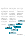
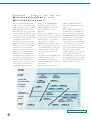
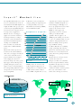
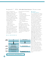
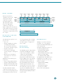
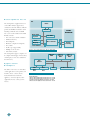
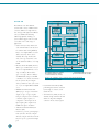
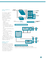
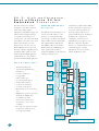
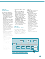
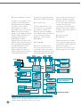
Fe b r u ar y
TM
3 2 - b i t
a n d
m i c r o c o n t r o l l e r s
m i c r o p r o c e s s o r s
S y s t e m
S o l u t i o n s
1 9 - 0 4 0 A
2 0 0 0
TM
INDEX
i n t r o d u c i n g
t h e
Welcome
2
SuperH™
3
Architecture Evolution
SuperH™
4
Family of 32-bit
S u p e r H ™
f a m i l y
Microcontrollers and
Microprocessors
SuperH™
5
32-bit Embedded Controllers
SuperH™
SH-5
6
32-bit Embedded Processors
SuperH™
7
Market View
SH-4
SH3-DSP
SuperH™
8
CPU Architecture Overview
SH-1:
13
Low-cost, Highly-integrated
SH-3
32-bit Embedded Controllers
SuperH™
SH-DSP
15
Family Devices
SH-2
SH-2:
19
Advanced 32-bit Embedded
Controllers
SH-3:
SH-1
24
High-performance,
Cost-effective 32-bit
Embedded Processors
SH-4:
27
The Next Wave of
Embedded Computing
Reader’s Guide
This document provides an overview of Hitachi’s 32-bit SuperH™ embedded
microcontrollers and microprocessors.This document includes 3 main sections.The 1st
covers general overviews and some background information.The 2nd introduces the
SuperH™ CPU architecture providing an overview of the most relevant technical
details. Finally, section 3 provides in-depth discussions of the individual SuperH™
series.You will also find tables helping you to select the right SuperH™ device for
your application.
We strongly recommend you read all sections before making your decision.
1
W e l c o m e
Creating the information society with all
knowledge we collected by developing
its new products and services is one of
and marketing 4-, 8- and 16-bit
the biggest challenges of this decade. As
embedded controllers, LCD controllers,
one of the major players in the global
ASIC technology, memory devices, and
electronic’s industry, Hitachi is
LCD displays.
committed to play a very active role to
The next pages will guide you through
build this information society.
the most important features of Hitachi’s
Hitachi’s general strategy is working
SuperH™ 32-bit embedded
closely together with its customers at the
microcontroller and microprocessor
leading edge for all of its products and
family and will provide useful
services while providing a maximum of
background information.
quality and reliability.
Advanced and next-generation
microprocessors play a very important
role in products and services for the
information society. Hence, Hitachi
developed an advanced 32-bit RISC
processor family called SuperH™.
This 32-bit processor family is based on a
broad range of devices optimised for a
wide variety of applications.
It is not sufficient just to provide
leading-edge technology to make
processors a success. With this in mind,
Hitachi also offers technical support,
software, and tools helping customers and
partners get their products on the
market.What is more, Hitachi even
establishes global partnerships to enhance
support and quality of products and
services.
This explains that the SuperH™ 32-bit
processor family is one of the leading
architectures in the world.
Currently offering devices from 10 to
360 MIPS, the SuperH™ series can be
used as basis for low-end embedded
control applications up to high-end
products with stringent performance
requirements.
When offering SuperH™ solutions to
our customers we benefit from the wide
2
S u p e r H ™
A r c h i t e c t u r e
E v o l u t i o n
Choosing a microprocessor leads to a
has been created for 32-bit embedded
Based on these architectures, Hitachi
long-term relationship between user and
control applications requiring a high
offers leading-edge 32-bit
microprocessor provider.Thus, several
performance at very low costs combined
microcontrollers and processors and is
criteria play a decisive role for the
with an integration of peripherals and
steadily developing further products to
success of a microprocessor architecture.
on-chip RAM and ROM.The SH-2
ensure that you are always at the leading
It is not only the technical leadership, it
enhances the SH-1 mainly by offering an
edge.
is also the support environment as well as
extended instruction set and a cost-
Hitachi is also a forerunner in combined
the processor roadmap where users have
optimised cache mechanism.
CPU and Digital Signal Processor (DSP)
to co-operate with the provider for a
The higher performance SH-3 features
architectures.The SH-DSP and SH3-
long time.The facility to switch from
an extended SH-2 instruction set, a
DSP architectures feature an integrated
low-cost to a very high-performance
memory management unit, additional
single architecture approach for general
device with a minimum of redesign
register banks, extended cache
purpose microcontroller and DSP tasks.
effort can be a crucial factor for the
mechanisms and dedicated peripherals.
While the SH-DSP extends the
future success.
The SH-4 is currently introduced to give
instruction set of the SH-1 and SH-2,
This is not restricted to, but especially
the user a maximum of throughput and
the SH3-DSP’s instruction set is a
true for the 32-bit embedded domain.
performance for next generation high-
superset of SH-1, SH-2, SH-3 and SH-
Maybe the most important feature of the
end embedded multimedia applications.
DSP, also offering instruction set upward
SuperH™ processor family is the
When writing code for the SH-1 it can
compatibility.
availability of a series of upward
be re-used in object-code format even
compatible architectures being optimised
for the SH-4. This kind of software
for a lot of different applications and
re-usability helps Hitachi to shorten the
markets.
design-cycle of new products and helps
The SuperH™ - also simply called SH -
partners to stay at the forefront of
provides even object-code upward
application development while reducing
compatibility throughout the family.
the overall costs.
SH-5
Based on a common 32-bit RISC
architecture, Hitachi developed
SH-4
the SH-1 architecture, further
extended by SH-2, SH-3 and
SH-4.The SH-1 architecture
SH3-DSP
SH-3
SH-DSP
SH-2
SH-1
Figure 1: SuperH™ Architecture Evolution
3
S u p e r H ™ F a m i l y o f 3 2 - b i t
M i c r o c o n t r o l l e r s a n d
M i c r o p r o c e s s o r s
The previously introduced SuperH™
members of the SuperH™ family for
MIPS, the SuperH™ family offers
family is defined by the main line SH-1
industrial automation as well as for
devices for nearly all 32-bit embedded
to SH-4 and includes a sub-line, the SH-
multimedia applications such as video
applications.
DSP and SH3-DSP architecture line.
game consoles and lots of other
Besides offering standard devices such as
These architectures can be separated into
applications.
the SH7040 line (see below)Hitachi is
a major embedded controller line and an
Because of the compatibility across the
also a leader in ASIC technology.With
embedded processor line.The embedded
family, users have the security of finding
the CBIC and µCBIC approach Hitachi
controller line is based on the SH-1, SH-
the right device for different applications
created the basics to enable efficient
2, and SH-DSP architectures, the
while reducing the costs of redesign or
ASIC design and system-on-a-chip
embedded processor line on the SH-3,
learning curves to a minimum.
solutions based on the SuperH™ CPU
SH3-DSP and SH-4 architecture. Figure
SuperH™ represents a family of devices
core family. A library of state-of-the-art
2 provides an overview of the individual
which focused right from the start and
modules and an open system design
implementations separated into the
across all family members on low-power
approach enables Hitachi together with
aforementioned controller and processor
consumption, high code density, high
customers to provide optimised
line and gives a first indication of the
level of integration and system cost
controller solutions in a very early stage
performance of the individual devices.
reduction.
of the overall product design cycle.
Several lines have been designed to offer
Thus, members of the SuperH™ product
The µCBIC approach is not restricted to
cost reductions by integrating special
family are leaders in the 32-bit
the 32-bit SuperH™ CPU core family,
application-oriented peripherals for
embedded arena in terms of power
also 16-bit H8/300H and H8S cores are
dedicated markets. Users can chose from
consumption (MIPS/Watt), code density
available for further integration.
a huge number of compatible devices
and system costs.
and derivatives.Thus, users will find
While spanning a range from 10 to 360
SH5 CORE
1000 MIPS
SH4 CORE
360 MIPS
µCBIC
SH3-DSP CORE
133 MIPS/266 MOPS
µCBIC
SH1 CORE
20 MIPS
SH7729
EM
BE
DD
ED
PR
OC
ES
SO
RD
EV
ICE
S
IC E
µCB
SH2 CORE
28 MIPS
VOL
UTIO
N
SH-DSP CORE
60-133 MIPS
SH-DSP CORE
60 MIPS/120 MOPS
SH7750
SH7709
SH7709A
µCBIC
SH7718
SH7708
ES
C
VI
R
LE
SH7612
OL
R
NT
CO
SH7604
O
CR
I
D
DE
M
DE
SH7410
SH7050
SH7040
SH7065
SH7055
SH7010
D
µCBIC
EM
BE
SH7020
SH7030
Figure 2: SuperH™ CPU Family Overview
4
S u p e r H ™
3 2 - b i t
E m b e d d e d
C o n t r o l l e r s
Embedded Controllers need a clear focus
Cost plays the decisive role throughout
the SH-DSP series offering an extended
on high integration, high code density, as
the embedded controller line. A set of
instruction set to serve the need for
well as low power consumption.The
peripherals integrated into the members
additional DSP performance with a
SH-1, SH-2, and SH-DSP have been
of the series provides glueless connection
single architecture.
designed and are continuosly further
to a huge variety of external devices or
developed for the 32-bit embedded
even makes external devices obsolete in
control market.Thus, the SH 32-bit
many cases. Several members of the SH-
embedded controller line focuses on
2 series have been designed for dedicated
integrated memory, integration of
applications to even improve the
peripherals and cost-optimised system
performance and to reduce the system
design.The members of the embedded
costs for special applications.
controller line are available with up to
Figure 3 shows the various members of
256 kBytes of integrated FLASH ROM
the SH-1 and SH-2 series.The SH-2
and up to 10 kBytes of RAM. Also
series has been extended by
versions are available.
SH7050F
INTEGRATION
SH7051F
SH2 Core, 32x32
+ 64-bit MAC,
256k/128k FLASH
10/6k RAM ATU,
SCI x 3, CMT, APC,
16ch A/D, DMAC x 4,
Automotive ASSP
SH-2E Core,
32 x 32 + 64-bit MAC
512k FLASH,
32k RAM
FPU, ATU-II
APC, HCAN x 2
CMT, DMAC x 4
SCI x 5, A/D x 3
AUD, H-UDI
256 pin
40MIPS 5/3.3V
SH7017F
SH7016
SH7045F
SH7034
168 pin 20MIPS/5V
SH7044F
SH1 Core, 16x16
+ 42-bit MAC,
64k/4k ROM/RAM,
ITU, TPC,
DMAC x 4, A/D,
SCI x 2
SH7041
SH7043
SH2 Core, 32x32
+ 64-bit MAC,
128k/64k ROM
4k RAM or 1k/1k
RAM/Cache, MTU,
CMT, DMAC x 4,
A/D, SCI x 2, DTC,
Motor Control ASSP
112 pin 20MIPS/5V
12.5MIPS/3.3V
SH7032
SH1 Core, 16x16
+ 42-bit MAC,
ROMless 8k RAM,
ITU, TPC,
DMAC x 4, A/D,
SCI x 2
144 pin 28MIPS/5V
16MIPS/3.3V
SH7040
112 pin 20MIPS/5V
12.5MIPS/3.3V
176 pin 60MIPS
SH7055F
PROM, mask ROM and ROMless
Figure 3:
SuperH™ Embedded
Microcontroller
Family Tree
SH706x
SH-DSP Core,
FLASH,
RAM
Multiple Timers
ADC
SCI's
SH7042
SH7021
SH1 Core, 16x16
+ 42-bit MAC,
32k/1k ROM/RAM,
ITU, TPC,
DMAC x 4,
SCI x 2
100 pin 20MIPS/5V
12.5MIPS/3.3V
SH2 Core, 32x32
+ 64-bit MAC,
128k/64k ROM
4k RAM or 1k/1k
RAM/Cache, MTU,
CMT, DMAC x 4,
A/D, SCI x 2, DTC,
Motor Control ASSP
SH2 Core, 32x32
+ 64-bit MAC,
4k/1k RAM/Cache,
256k FLASH
MTU, CMT,
DMAC x 4,
A/D, SCI x 2,
Motor Control ASSP
SH2 Core, 32x32
+ 64-bit MAC,
64k ROM/128k FLASH,
3k/4k RAM/Cache,
MTU, CMT, DMAC x 2
SCI x 2, A/D
112 pin
28MIPS/5V
SH7011
112/144 pin
28MIPS/5V
16MIPS/3.3V
SH7014
SH2 Core, 32x32
+ 64-bit MAC,
ROMless
3k/1k RAM/Cache,
MTU, CMT,
DMAC x 2,
SCI x 2
SH2 Core, 32x32
+ 64-bit MAC,
ROMless
4k RAM,
MTU, CMT,
8-bit timers x 2
SCI, A/D
100 pin
20MIPS/3.3V
112 pin
28MIPS/5V
16MIPS/3.3V
112 pin 28MIPS/5V
16MIPS/3.3V
SH7020
Part Number
Core
MAC Resolution
ROM/RAM,
Peripherals
SH1 Core, 16x16
+ 42-bit MAC,
16k/1k ROM/RAM,
ITU, TPC,
DMAC x 4,
SCI x 2
100 pin 20MIPS/5V
12.5MIPS/3.3V
A/D
APC
ATU
CMT
DMAC
DTC
H-UDI
= Analogue to digital converter
(10-bit resolution)
= Advanced Pulse Controller
= Advanced Timer Unit
= Compare Match Timer
= Direct Memory Access Controller
= Data Transfer Controller
= Hitachi user Debug Interface
ITU
MAC
MTU
SCI
SIO
TPC
= Integrated Timer Unit
(5 channels x 16-bits)
= Multiply and Accumulate
= Multifunction Timer Unit
= Serial Communications Interface
= Serial Input/Output
= Timing Pattern Control
5
S u p e r H ™
3 2 - b i t
E m b e d d e d
P r o c e s s o r s
The SuperH™ embedded processor line
Units and other peripherals. Members of
SuperH™ embedded processor line is a
of Hitachi has been designed to match
the embedded processor line have been
leader in the Windows® CE area
the needs of advanced embedded
designed for consumer applications such
offering optimised and complete system
computing requirements. Starting with
as PC companions or other handheld
solutions for PC companions as well as
the SH-3 architecture, extended by the
devices. Other application areas are
other Windows® CE based systems.
SH3-DSP and the SH-4 CPU core a set
telecommunication, multimedia and
of compatible devices has been created
automotive applications. Figure 4 gives
for the needs of embedded processor
an overview of the various members of
applications of today.The SuperH™
the embedded processor line.The
embedded processor line features, for
SH7751
example, high-performance cache
SH7750*
mechanisms or Memory Management
SH4 Core,
Superscaler
8/16/32/64 bit Bus
FPU, Graphics, MAC
8k + 16k Cache
MMU, SCI x 2, RTC
DMAC, SDRAM,
PCMCIA
Bus Interface
Timer
Figure 4: SuperH™
Embedded Processors
Family Tree
SH7709*
SH3 µCBIC Core*
PERFORMANCE
SH3 Core,
Single Precision
Floating Point
8k Cache
SH7708*
SH3 Core,
8/16/32 bit Bus
32x32
+ 64-bit MAC,
8k Cache
MMU, SCI x 1,
RTC Timers,
SDRAM/PCMCIA
Bus Interface
SH3 Core,
8/16/32 bit Bus
32x32
+ 64-bit MAC,
8k Cache
MMU, SCI x 3, RTC,
DMAC, SDRAM,
PCMCIA
Bus Interface
A/D, D/A, Timers
256 pin
360MIPS/1.8V
SH7709A*
SH7729*
SH3-DSP Core,
8/16/32 bit Bus
DSP Unit, 16k Cache
16k RAM,
MMU, SCI x 3, RTC,
DMAC, SDRAM,
PCMCIA
Bus Interface
Timer
133MIPS
208 pin
133MIPS/266 MOPS
208 pin 80MIPS/3.3V
SH7718
SH-3E Core,
Single Precision
FPU
144 pin 60MIPS/3.3V
100MIPS/3.3V
SH7702
SH7604
SH2 Core,
8/16/32 bit Bus
32x32
+ 64-bit MAC,
4k Cache
Hardware divider
SDRAM Interface
DMAC x 2
SCI x 1, Timers
144 pin 25MIPS/5V
16.6MIPS/3.3V
SH3 Core,
8/16 bit Bus
32x32
+ 64-bit MAC,
2k Cache
MMU, SCI x 1,
RTC Timers,
SDRAM/PCMCIA
Bus Interface
120 pin 60MIPS/3.3V
MAC
SDRAM
SCI
DMAC
RTC
MMU
=
=
=
=
=
=
Multiply and Accumulate
Synchronous DRAM
Serial Communications Interface
Direct Memory Access Controller
Real Time Clock
Memory Management Unit
* Designed for WindowsCE™
6
Part Number
CPU Core
Bus Width
MAC Resolution
Cache
Peripherals
S u p e r H ™
M a r k e t
V i e w
The SuperH™ CPU family is one of the
At Hitachi, we went even further by
competitive price. Software ranges from
most successful architectures in the 32-
setting up a European engineering and
Assembler, an ANSI C-Compiler via a
bit embedded domain.With shipments of
tool design subsidiary 12 years ago:
C-level debugger to MakeApp, a tool
roughly 20 million units per year (based
Hitachi Microsystems Europe (HMSE)
that sets up peripherals and creates driver
on 1997 data) the SuperH™ family has a
based in Maidenhead (UK).
routines on the click of a mouse.
HMSE also offers support and
broad customer base using these devices
in a huge variety of applications.
S h i p m e n t s
S u p e r H ™
M units
engineering resources for customers
Hitachi is also the second biggest
22
wishing to use Hitachi’s ASIC
supplier of 16-bit microcontrollers to
20
capabilities.This also applies to our
the European market (according to
18
µCBIC program, enabling our customers
Dataquest), as well as the third for 4bit, sixth for 8-bit. Hitachi produces
and ships over 12 million H8
microcontrollers every month, this
includes almost 4 million H8 Flash
to select one of Hitachi’s CPU cores and
16
combine it with peripherals from our
14
library and adding customer specified
12
10
SuperH
logic via VHDL or Verilog.
In addition, Hitachi is also establishing
devices.
8
strategic partnerships with other key
Hitachi semiconductor products are
6
players in the embedded world to ensure
used all over the world and Hitachi
4
the future success and evolution of the
offers services and support in nearly all
product lines in the growing embedded
corners of the world.This ensures a
marketplace.
proper worldwide sales and support
service helping the customers to
shorten the design cycle and to get the
1994 1995 1996 1997 1998
Figure 5: SuperH™ Shipments over
the years
But after all we do not forget, it is the
customer who decides if a
microprocessor line is successful. More
than 2000 design-wins illustrate that the
right support in time. Hitachi partner’s
providing third-party assistance and
HMSE provides our customers with
SuperH™ is the right choice for a huge
support can also be found throughout
locally designed and supported tools
variety of applications. Hitachi is
the world providing additional resources
ranging from low cost evaluation boards
committed to further extend the product
and capacities for your system design
to fully featured real time emulators
line to stay at the forefront of the
based on SuperH™.
based on IBM-compatible PC’s at a very
business and technology of tomorrow.
Communication
6%
Industrial 49%
OA-Computer 27%
Consumer
18%
SGS Thomson
Microelectronics
Epson
Sony
Figure 6:
SuperH™ Design Win Overview by
Product Classification
Figure 7: Strategic Alliances
for SuperH™
7
S u p e r H ™
C P U
A r c h i t e c t u r e
O v e r v i e w
All devices in all families in the
The SH architecture has the following
Re g i s t e r
SuperH™ series employ a common 32-
basic features:
C o n f i g u r a t i o n
bit RISC (Reduced Instruction Set
• Load/Store architecture
In case of the SH architecture, arithmetic
Computer) architecture, designed
• 32-bit internal data path
and logical instructions operate normally
specifically by Hitachi to meet the needs
• General Purpose 32-bit Register bank
on the 32-bit general purpose registers.
of next-generation applications.This
• 32-bit Control Registers
Special load/store instructions are
architecture is implemented in the SH-1
• 32-bit System Registers
provided to transfer data from memory
series.The SH-2, SH-3, and SH-4 feature
• RISC-type instruction set
to registers and vice versa. Figure 8
upwardly compatible extensions.
• 16-bit fixed-length instruction set
below shows the basic General Purpose
Typically, RISC architectures feature:
• 4 Gbyte address space
32-bit register bank which is used for
• Load/Store approach
• Basic 5-stage RISC instruction
source and destination operands.The
• Register orientation
pipeline
SH-3, SH3-DSP and the SH-4
• Simple instruction set
The address space is uniform and
architecture feature in addition to the
• Uniform instruction issuing
unsegmented.The instruction set has
basic 16 registers, 8 32-bit shadow
• Instruction pipelining
been carefully chosen to provide a high-
registers which can be accessed in the
These basic features have been extended
level language orientation, thus
so-called privileged mode. Besides the
by Hitachi to meet the requirements of
simplifying programming of the
general purpose registers, the SH
modern embedded applications. For
individual devices. All basic SH CPU
architecture provides 4 System Registers
example, Hitachi introduced in the SH
cores feature the integration of power
providing a Program Counter (PC),
architecture a fixed 16-bit instruction
saving strategies and implement methods
Procedure Register (PR), and 2 32-bit
length offering a very high code density
to control the power consumption of
Multiply and Accumulate Registers
and thus saving memory and instruction
peripherals.
(MACH/MACL). A block of Control
fetch bandwidth.
Registers finally completes the set of
registers in the basic SH architecture.The
B a s i c
S H
Fe a t u r e s
Control Register Block contains the
Status Register (SR), the Global Base
Register (GBR), the Vector Base
Register (VBR) , and in case of SH-3,
31
GENERAL
PURPOSE
REGISTERS
0
31
RO
R1
R2
0
RO (Shadow Registers)
SH3-DSP and SH-4 the Saved Status
Register (SSR), and the Saved Program
Counter (SPC) .
R2
The General Purpose Register R0
functions as index register for indirect
R7
R13
R14
indexed addressing modes (see below).
R15, SP (Stack Pointer)
31
CONTROL
REGISTERS
SYSTEM
REGISTERS
In the case of SH-1, SH-2, and SH-DSP
0
31
SR (Status Register)
GBR (Global Base Register)
VBR (Vector Base Register)
0
SR (Saved Status Register)
hardware stack pointer (SP). Register
operands are always 32-bit longwords.
31
0
MACH (Multiply and Add Accumulator High)
MACL (Multiply and Add Accumulator Low)
PC (Procedure Register)
31
PROGRAM
COUNTER
0
PC (Program Counter)
ALL
When the memory operand is only a
byte or a 16-bit word, it is sign-extended
31
0
SPC (Saved Program Counter)
SH3, SH3-DSP, SH4
Figure 8: SH Architecture General Purpose Register
Bank, Control Registers, and System Registers
8
the register R15 is also used as a
into a longword when loaded into a
register.
I n s t r u c t i o n
Set
The advantage of the used RISC
does not need all stages, and extended if
approach can be seen by pipeline
an instruction needs some more latency
One main strength of the SH processor
mechanism allowing very high clock
cycles to be completed or if pipeline
family is the instruction set upward com-
frequencies.
contention occurs.To reduce pipeline
patibility of the various CPU cores.
The SH’s pipelining mechanism provides
penalties, a delay-slot mechanism has
Figure 9 gives an overview of the
a single cycle peak throughput for the
been provided, reducing pipeline-
instruction set compatibility.The basic
basic instructions (2 in case of the
breakages.
SH instructions are all 16 bits long and
superscalar SH-4). For that purpose, the
The instruction set can be classified into
thus tentatively offer a twice as efficient
SH architecture is using a basic 5-stage
the following operation categories:
code density compared to conventional
pipeline, see Figure 10.The pipeline is
• Data transfer
32-bit RISC architectures.
automatically reduced if an instruction
• Arithmetic
• Logical
• Shift
• Branch
• System control
SH3-DSP
160 types
MMU & DSP instructions
SH-DSP
DSP instructions
• Extended such as Floating Point or
DSP operations (not for SH-1, SH-2,
and SH-3)
154 types
The data transfer instructions can be used
SH-1
SH-2
SH-3
SH-4
56 types
62 types
68 types
91 types
32-bit
multiplier/
accumulator
MMU instructions
FPU, Graphics
instructions
with following addressing modes:
• Direct register addressing
• Indirect register addressing
• Postincrement indirect register
addressing
Figure 9: Instruction Set Upward Compatibility
• Predecrement indirect register
addressing
: Slot
Instruction A
IF
Next instruction
ID
EX
IF
ID
EX .....
IF
ID
Third instruction in series
• Indirect register addressing with
displacement
• Indirect indexed register addressing
EX .....
• Indirect GBR addressing with
: Slot
MULS.W
IF
Next instruction^)
ID
EX MA mm mm
IF
ID
EX MA WB .....
IF
ID
Third instruction^)
displacement
• Indirect indexed GBR addressing
• Indirect PC addressing with
EX MA WB .....
displacement
: Slot
Instruction A
IF
Next instruction
Third instruction in series
EX
IF
ID
EX .....
IF
ID
=
=
=
=
Instruction Fetch
Instruction Decode
Execution
Memory Access
• PC relative addressing
• Immediate addressing
Figure 11 illustrates an example of the
EX .....
IF
.....
IF
ID
EX
MA
ID
ID
EX .....
WB = Write Back
mm = Multiplier Operation
^) = If instruction also uses the
multiplier pipeline, contention
can occur
various addressing modes.This set of
addressing modes allows an efficient
code generation of modern compilers.
Figure 10: Instruction Pipelining, Examples
9
I n s t r u c t i o n
D e s c r i p t i o n
The effective address is the content of register Rn. A constant is
added to the content of Rn after the instruction is executed. 1 is
added for a byte operation, 2 for a word operation, and 4 for a
longword operation
Fe t c h
Besides optimising the costs for storage
media, the fixed 16-bit instruction length
Rn
also solves the bottleneck problem of
Rn
conventional 32-bit RISC architectures.
On a 32-bit memory access, 2
instructions can be loaded in parallel
E q u a t i o n
+
Rn (After the
instruction is
executed)
Byte: Rn + 1 ➙ Rn
Word: Rn + 2 ➙ Rn
Longword: Rn + 4 ➙ Rn
1/2/4
reducing the necessary memory accesses
by a factor of 2.
M U L / M A C
O p e r a t i o n
The SH architecture and thus all SH
devices include a hardware multiplier
providing a very high arithmetic
Figure 11: Postincrement indirect register addressing mode
performance.The multiply instruction
A p p l i c a b l e
I n s t r u c t i o n s
Class
Operation Code
Function
Data
transfer
MOV, MOVA, MOVT.
SWAP, XTRCT
Data transfer
✓
Arithmetic
operations
ADD, ADDC, ADDV,
CMP/cond, DIV1,
DIVOS, DIVOU, EXTS,
EXTU, MAC, MULU,
MULS, NEG, NEGC,
SUB, SUBC, SUBV
Add, Subtract, Multiply,
Divide (initialize and
step),
Multiply-And-Accumulat
e, Negate, Extract
MUL, DMULS, DMULU.
DT
Double-Length Multiply,
Decrement-and-Test
Logic
operations
AND, NOT, OR, TAS,
TST, XOR
Bitwise logic operations,
Memory Test-And-Set,
Bit Test
✓
Shift
ROTL, ROTR, ROTCL,
ROTCR, SHAL, SHAR.
SHLL, SHLLn, SHLR,
SHLRn
Rotate, Shitt-one-bit
(arithmetic/logical),
Shift-n-bits (logical,
n=1,2,8, or 16)
✓
SHAD, SHLD
Shift-n-bits dynamic
(arithmetic/logical, 325≤ n≤ 31 )
Branch
System
control
BF, BT, BRA. BSR,
JMP, JSR, RTS
Conditional branch
unconditional
branch/calLjump/return
with delayslot
BRAF, BSRF, BF/S.
BT/S
Far branch/call,
conditional branch with
delayslot
CLRT, CLRMAC, LDC,
LDS, NOP, RTE, SETT.
SLEEP, STC, STS.
TRAPA
Clear T-bit
LDTLB, PREF, SETS.
CLRS
Total
Table 1: SH Instruction set overview
10
(MUL) operates on register contents and
SH
-1
✓
SH
-2
SH
-3
#Instruction
s /#Types
✓
✓
SH-1: 39/5
SH-2: 39/5
SH-3: 40/6
✓
✓
SH-1: 26/17
SH-2: 33/21
SH-3: 34/21
stores the data in the dedicated system
registers MACL/MACH.The multiplyaccumulate instruction (MAC) directly
operates on memory locations.The result
is stored as before in the system registers.
This is especially useful as the MAC
instruction operates normally on a big
✓
linear set of data. General Purpose
✓
registers are used for storing the current
✓
✓
14/6
memory addresses, which are
automatically updated upon completion
✓
✓
SH-1: 14/10
SH-2: 14/10
SH-3: 16/12
of a MAC instruction.
I m m e d i a t e
D a t a
✓
The SH architecture provides a very
✓
✓
✓
✓
efficient mechanism to process
SH-1: 7/7
SH-2: 11,9
SH-3: 11/9
immediate data values. Byte immediate
data are directly located in the 16-bit
instruction code.Word or longword
✓
immediate data are stored in a memory
table, which can be accessed by an
✓
✓
✓
SH-1: 31,11
SH-2: 31,11
SH-3: 74/14
immediate data transfer instruction.
When the immediate data is loaded, the
value is transferred to the register bank.
✓
SH-1: 133/56
SH-2: 142/62
SH-3: 189/66
D a t a
Fo r m a t
Memory data formats are
classified into bytes, words,
and longwords.The SH
architecture is basically a
big-endian machine, but
Address
A
Address
A+4
Address
A+8
Address Address
A
A+1
Address
A+2
Address
A+3
Address Address
A+11
A+10
Address
A+9
Address
A+8
31
15
7
31
15
7
23
0
Byte0 Byte1 Byte2 Byte3
Word0
SH-3, SH3-DSP and SH-4
23
0
Byte3 Byte2 Byte1 Byte0
Word1
Word1
Word0
Longword
Longword
Big endian
Little endian*
Address
A+8
Address
A+4
Address
A
devices also support littleFigure 12: Memory data formats, Byte, Word, and Longword Alignment
endian mode, see Figure 12.
* o n l y S H - 3 , S H - 3 - D S P, S H - 4
Figure 13 illustrates the data format of
registers.When the memory operand is
only a byte or a 16-bit word, it is signextended into a longword when loaded
31
0
Longword
into a register
Figure 13: Longword Register Operand
P r o c e s s o r
a n d
S t a t e s
M o d e s
Pe r i p h e r a l s
The SH architecture provides a set of
user mode, privileged mode is normally
processor states:
entered when an exception occurs. Also
• Reset state
the shadow registers, see Figure 8, are
All SH processors feature around the
• Exception handling state, transient
then accessible.
basic CPU core a set of peripherals.
Details of the individual SH families and
state during which the CPU’s
processor state flow is altered by a
Exc epti on
series are listed below.
reset, general or interrupt exception
P r o c e s s i n g
Nevertheless, all SH devices feature a set
of common peripherals, such as:
• Program execution state
The SH family provides a single, uniform
• Interrupt Controller (INTC)
operation and power consumption is
mechanism for handling all exceptions,
• Watchdog Timer (WDT)
reduced
• Power-down state, CPU halts
wether caused by hardware or software
• Serial Communication Interface (SCI)
• Bus-released state, the CPU has
conditions. Exception handling is
• Bus State Controller (BSC)
released the bus to a device that
resolved around a single table, the
• User Break Controller (UBC)
requested it
Excpetion Vector Table.The Vector Base
The implementation may differ between
All SH devices have built-in power-
Register (VBR) points to the beginning
individual devices. In addition to these
down modes:
of that table. Exception conditions are
peripherals, various devices in the series
• Sleep, on-chip peripherals still run
prioritized by dedicated hardware. An
provide for example:
• Standby, on-chip peripherals halt
Exception Handler, which is a kind of
• DMA Controller (DMAC)
• Module stand-by (only SH-3, SH3-
hardware-dispatched subroutine call,
• Parralel I/O Ports
automatically stores and restores registers.
• Real-Time Clock RTC)
DSP, SH-4), specified modules halt
The details of the exception processing
• A/D Converter (ADC)
The SH-3, SH3-DSP, and SH-4
depends on the individual architecture
And a lot more other peripherals.
architecture incorporate 2 processor
implementation and by the implemented
modes: user mode and privileged mode.
Interrupt Controller (INTC), for further
Normal program execution is done in
details see below.
11
D S P
E x t e n s i o n s
Figure 14 illustrates the advances of the
D S P
v s .
M A C
integrated CPU/DSP approach over
Fu n c t i o n a l i t y
In more and more embedded control
traditional approaches.
applications it is necessary to include so-
In the SH-DSP and SH3-DSP
For several applications it is sufficient to
called Digital Signal Processing (DSP)
architecture, Hitachi added mainly:
use the SH’s integrated MAC
capabilities. In traditional approaches this
• an additional X-Y-on-chip bus
functionality and accelerator, respectively.
has been solved by adding to the
structure
As this MAC has been optimised for
microcontroller-system a dedicated DSP
• loop hardware
memory accesses, it is especially useful
processor which differs a lot from
• fixed-point arithmetic support
for running filter algorithms. This
traditional microcontrollers and
• DSP-oriented addressing modes
already offers enough performance for
microprocessors.The architecture of DSP
• an DSP-oriented instruction set
several DSP algorithms.With the SH-
processors is normally memory-oriented,
extension.
DSP and SH3-DSP, the SH family will
includes special addressing modes and the
The SH-DSP architecture offers object-
offer alternatives to run DSP algorithms
DSP processors’ instruction set is
code upward compatibility from the SH-
if a higher performance is required.
focusing on the processing of DSP
1 and SH-2 architecture, the SH3-DSP
algorithms such as Finite or Infinite
from the SH-1, SH-2, SH-DSP and
Impulse Response Filters (FIR/IIR), or
SH-3 architecture providing an easy
the Fast Fourier Transform (FFT). Based
upgrade path for future products.
Figure 14:
Conventional vs.
Integrated
CPU/DSP System
Solution Approach
on such basic algorithms, DSP processors
are , for example, especially useful for
modem algorithms, and audio or image
processing software.
The classical approach, using a
Program 1
Control
panel display
and other
functions
Program 2
Analog
I/O, others
DSP
Processor
Controller
microcontroller and a dedicated DSP
Register Bank
Control
panel display
and other
functions
Analog
I/O, others
Program
(single instruction
stream)
ALU
RAM
DSP MAC
CPU/DSP processor
processor leads to complex systems, with
very often 2 operating systems, and
Memory
Memory
several heterogeneous bus systems which
often make system design and debugging
very difficult.Within the SuperH™
family a new and innovative approach
IAB
Address
Main
Bus
SH-DSP
32
YAB
16
Figure 15:
SH-DSP Integrated
DSP Unit Functional
Block Diagram
16 x 32 bit
General Purpose
Register File
X AB
16
has been designed offering an integrated,
combined CPU/DSP architecture
approach. Based on the SH-2 CPU core,
Hitachi added dedicated DSP capabilities
DSP REGISTER SET
resulting in the SH-DSP core concept.
The same is being done with the SH-3
RISC
or
DSP(Y)
Memor y
core, resulting in the advanced SH3-DSP
CPU core.
8 x 32 bit
Data
Register File
RISC
or
DSP(X)
Memor y
ALU
Users now have 2 cores integrated in a
single architecture with a single
Add-ALU
Flexible Memor y
for Data/Program
(ROM or R AM )
instruction stream.This simplifies system
Decoder
design and offers an overall cost
ALU Barrel Shifter
utilisation of additional and expensive
cases.
12
Mult
16/32 Prefetch Unit
reduction.This approach makes the
accelerator hardware superfluous in most
Control
Signal
Main
Data
Bus
IDB
16 YDB
16
32
S H - 1 : L o w - c o s t , H i g h l y I n t e g r a t e d
3 2 - b i t E m b e d d e d C o n t r o l l e r s
The SH-1 series forms the basis of the
• Multiplication operations (16x16(32)
SuperH™ embedded controller family.
executed in 1-3 cycles, multiplication
input capture, counter clearing, PWM
The members of this family have been
/accumulation operation
mode, phase counting, DMAC
optimised for low cost and high
(16x16+42(42) executed in 2-3
integration while offering the
cycles, 42-bit accumulator
performance of a 32-bit controller.The
• Processing states: program execution,
SH-1 series integrates on-chip RAM and
exception processing, bus release,
ROM. All SH-1 implementations
reset, sleep mode, standby
incorporate a 16-bit hardware multiplier,
activation
• Watchdog Timer (WDT) for
monitoring system operations
• Programmable Timing Pattern
Controller (TPC), maximum output
of 16-bit data, output can be enabled
which produces a 32-bit result.What is
C o m m o n
more, all SH-1 devices implement a 42-
Pe r i p h e r a l s :
S H - 1
bit accumulator for 16-bit data giving
on a bit-by-bit basis
• Serial Communication Interface
(SCI), 2 channels, supports clocked
you the performance needed in most of
• Interrupt Controller (INTC) for 8+1
the 32-bit applications of today.
S H - 1
processed, compare match waveform,
A r c h i t e c t u r e :
synchronous and asynchronous mode,
external and a set of internal interrupt
selectable bit rates via on-chip baud
sources, up to 16 priority levels can
generator, full duplex communication
be programmed
• User Break Controller (UBC)
• 4 Channel DMA Controller (DMAC)
• Parallel I/O Ports, 2 16-bit
• 32-bit internal data path
simplifying debugging of user
input/output ports, each port has a
• 16-bit fixed-length RISC-type
programs
register for storing pin data
instruction set
• Clock Pulse Generator (CPG)
• Load/Store architecture
supplying the LSI and external
• 5-stage pipeline
devices with clock pulses from a
• 4 Gbyte address space
connected crystal resonator or an
• 16 x 32-bit general registers
external clock
• 3 x 32-bit control registers
• 16-bit Integrated-Timer Pulse Unit
• 4 x 32-bit system registers
(ITU) with 5 channels, up to 12
• Basic instructions are executed in 1
different pulse outputs and 10
cycle
• Bus State Controller (BSC), for details
see below
• Pin Function Controller (PFC) is
composed of registers for selecting the
function of multiplexed pins
• Single cycle access on-chip ROM and
RAM (32-bit)
different pulse inputs can be
31
9
(sign extended)
0
MACH
MACL
31
Multiply and accumulate (MAC) registers high and low
(MACH, MACL): Store the results of multiply and accumulate
operations. MACH is sign-extended when read because only
the lowest 10 bits are valid.
0
Procedure register (PR): Stores a return address from a
subroutine procedure.
PR
31
0
PC
Program counter (PC): Indicates the fourth byte (second
instruction) after the current instruction.
Figure 16: SH-1 System registers
13
B u s
S t a t e
C o n t r o l l e r
Port A
Address
( B S C )
The BSC divides the address space into 8
PROM or
masked ROM
ROMless*
RAM*
SH-1
CPU Core
Direct Memory
Access Controller
Control
areas. A maximum of 4 Mbyte of linear
address space for each area can be
addressed (area 1 up to 16 Mbyte when
• 8-/16-bit external data bus
• On-chip ROM and RAM can be
accessed in 1 cycle (32-bit)
Interrupt
controller
• Wait states can be inserted using the
User break
controller
Address
The BSC supports the following features:
Clock Pulse Generator
set to DRAM).
Bus state
controller
WAIT pin
• Direct interface to DRAM, SRAM,
and ROM
• Supports parity check and generation
for data bus
16-bit
integrated-timer
pulse unit
×
Programmable
timing pattern
controller
2
A/D )
converter
Watchdog
timer
• Refresh counter can be used as 8-bit
Data/address
• Access control
Power/Ground
Serial communication
interface
(2 channels)
• Control signals
interval timer
Port C z)
S H 7 0 2 0
S e r i e s
The SH7020 series includes 1 Kbyte of
Port B
■ Peripheral address bus (24 bits)
■ Peripheral data bus (16 bits)
■ Internal address bus (24 bits)
■ Internal upper data bus (16 bits)
■ Internal lower data bus (16 bits)
RAM and is available with 16 and 32
Figure 17: Functional Block
Diagram of the SH7020/SH7030
series
1) see selection guide for details
2) only SH7030 series
Kbyte of ROM, also a ROMless version
version. In addition to the above
is available.
introduced peripherals, the SH7030
The SH7020 series includes all the above
series features :
mentioned peripherals.
• A/D Converter, 10 bits x 8 channels
• 8-bit input port, additional register for
S H 7 0 3 0
S e r i e s
storing pin data
The SH7030 series is available with 4
Individual SH7020/7030 devices are
and 8 Kbyte of RAM. It either has 64
available in extended temperature range
Kbyte of ROM or comes as ROM-less
qualification.
Product Name Part name 1)
SH7020
SH7021
SH7032
SH7034
HD6417020xx
HD6437020Sxx
HD6477021xx
HD6437021Sxx
HD6417032xx
HD6417034xx
HD6477034xx
HD6437034Axx
ROM
(kByte)
ROM type
RAM
(kByte)
16
32
32
64
64
Mask ROM
OTP
Mask ROM
OTP
Mask ROM
1
8
4
Frequency
(MHz=MIPS)
5V
20
3.3V
12.5
Table 2: SH-1 Series Microcontroller Overview
1)Part names differ for 5V and 3.3V devices, for
different package types, and for different
temperature ranges
2)Temperature range: -20 to +75 °C
3)Temperature below 50 °C
Typ.
Power
(mW) 2)
Typ. Sleep
Current
(mA) 2)
Typ. Standby
Current
(uA) 3)
Package
215
3.3V
30
0.01
100 TQFP
198
40
0.01
112 QFP/
120 TQFP
14
S H
F a m i l y
D e v i c e s
S H - 1
Device
Core
Fa m i l y
D e v i c e s
SH7020
SH7020S
ROMless
SH7021
SH7032
ROMless
SH7034
SH-1
SH-1
SH-1
SH-1
SH-1
Vcc (V) / Max. Clo
5 / 20
5 / 20
5 / 20
5 / 20
5 / 20
3.3 / 12.5
3.3 / 12.5
3.3 / 12.5
3.3 / 12.5
3.3 / 12.5
External Bus Width
16
16
16
16
16
External B
On-chip ROM (kByte)
16
32
64
On-chip ROM
Mask ROM Version
yes
yes
yes
Mask ROM
yes
yes
ZTAT (OTP
Vcc (V) / Max. Clock (MHz)
ZTAT (OTP) Version
F-ZTAT (Flash
1
1
1
8
4
13 / 9
13 / 9
13 / 9
13 / 9
13 / 9
DMA Controller (channels)
4
4
4
4
4
(if cache
Watch Dog Timer (channel)
1
1
1
1
1
Cach
On-chip RAM (kByte)
Interrupts (Internal/External)
On-chip RAM
Serial Communication Interface
2
2
2
2
2
Interrupts (Internal/
I/O Ports (including input-only)
40
40
40
40
40
DMA Controller (c
Timing Pattern Controller
yes
yes
yes
yes
yes
Watch Dog Timer
Integrated Timer Unit
yes
yes
yes
yes
yes
Serial Communication
Bus State Controller
yes
yes
yes
yes
yes
I/O Ports (including in
User Break Controller
yes
yes
yes
yes
yes
Multifunction Tim
Clock Pulse Generator
yes
yes
yes
A/D Converter (bits x channels)
Data Book
Package
yes
yes
Unit, (c
10 x 8
10 x 8
Compa
19-015A
19-015A
19-015A
19-011B
19-011B
Timer (c
TQFP-100
TQFP-100
TQFP-100
QFP-112
QFP-112
Advanced Pulse C
TQFP-120
Part Name
HD6437020xxx HD6417020xxx HD64x7021xxx HD6417032xxx HD64x7034xxx
Advanced T
Bus State C
User Break C
Clock Pulse G
A/D Converter (bits x c
D
Pa
15
S H - 2
Device
Core
ock (MHz)
Fa m i l y
D e v i c e s
SH7014
ROMless 1
SH70161
SH7017F1
SH70111
SH7040A
SH7041A
SH7042A
SH7043A
SH-2
SH-2
SH-2
SH-2
SH-2
SH-2
SH-2
SH-2
5 / 28.7
5 / 28.7
5 / 28.7
3.3 / 20
5 / 33
5 / 33
5 / 33
5 / 33
3.3 / 16
3.3 / 16
3.3 / 16
3.3 / 16
16
16
32
16
32
ROMless
64
64
128
128
yes
yes
16
Bus Width
16
16
M (kByte)
64
M Version
yes
128
P) Version
h) Version
yes
yes
yes
yes
yes
M (kByte)
e is used)
3 (1)
3(1)
4(2)
e (kByte)
1
1
2
4
4 (2)
4 (2)
4 (2)
4 (2)
1
1
1
1
/External)
43 / 7
43 / 7
43 / 7
43 / 7
44 / 9
44 / 9
44 / 9
44 / 9
channels)
2
2
2
2
4
4
4
4
(channel)
1
1
1
1
1
1
1
1
Interface
2
2
2
1
2
2
2
2
nput-only)
43
82
82
11
82
106
82
106
mer/Pulse
3
3
3
3
5
5
5
5
2
2
2
2
2
2
2
2
yes
yes
yes
yes
yes
yes
yes
yes
yes
yes
yes
yes
Generator
yes
yes
yes
yes
yes
yes
yes
yes
channels)
10 x 8
10 x 8
10 x 8
10 x 7
channels)
are Match
channels)
Controller
imer Unit
Controller
Controller
Data Book
Package
QFP-112
art Name
HD6417014RFxx
QFP-112
HD6437016Fxx
QFP-112
HD64F7017Fxx
1) Contact your local sales office for availability
QFP-100
HD6417011Fxx
10 x 8
10 x 8
10 x 8
10 x 8
19-033A
19-033A
19-033A
19-033A
QFP-112
HD6437040Axx
QFP-144
QFP-112
QFP-144
HD6437041Axx
HD64x7042Axx
HD64x7043AFxx
S H - 3
SH7044A
SH7045A
SH7044F
SH7045F
SH-2
SH-2
SH-2
SH-2
5 / 28
5 / 28
Fa m i l y
Device
Core
5 / 33
5 / 33
3.3 / 16
3.3 / 16
16
32
16
32
256
256
256
256
yes
yes
yes
yes
4 (2)
4 (2)
4 (2)
1
1
1
44 / 9
44 / 9
44 / 9
4
4
4
4
1
1
1
1
2
2
2
2
82
106
82
106
5
5
5
5
2
2
2
4 (2)
1
44 / 9
2
yes
yes
yes
yes
yes
yes
yes
yes
yes
yes
yes
yes
10 x 8
10 x 8
10 x 8
19-033A
19-033A
19-033A
19-033A
10 x 8
QFP-112
QFP-144
QFP-112
QFP-144
HD64x7044Afxx
HD64x7045Axx
HD64F7044Fxx
HD64F7045Fxx
Vcc (V) / Max. Clock (MHz)
D e v i c e s
SH7709
SH-3
3.3 / 80
External Bus Width
32
On-chip RAM (kByte)
(4)
Cache (kByte)
8 (4)
(if RAM mode is used)
Memory Management Unit
yes
Interrupt Controller
yes
External Interrupt Pins
7
DMAC (channels)
4
Watch Dog Timer (channel)
1
Serial Communication Interface
3
IrDA 1.0 Support
yes
Smart Card Support
yes
PCMCIA Interface Support
I/O Ports (including input-only)
32-bit Timer (channels)
yes
12 x 8-bit
3
Real Time Clock
yes
Bus State Controller
yes
SDRAM Interface
yes
User Break Controller
yes
Clock Pulse Generator
yes
A/D Converter (bits x channels)
10 x 8
D/A Converter (bits x channels)
8x2
Litte-endian Support
yes
Big-endian Support
yes
Data Book 19-029C 19-036
19-036
Package LQFP-144 QFP-208
QFP-208
Part Name
HD6417709F80B
D e v e l o p m e n t
To o l s
PC
The development of applications based
PCIF3
on the SH-1 family is supported by
evaluation boards and emulators. Hitachi
provides the EVB7032 evaluation board
Host IF
TARGET
featuring a SH7032 device and PCE
HARDWARE
low-cost in-circuit emulators.The PCE
Emulators feature
Break Point
System
User RAM
• Emulation memory
Trace
• PC breakpoints
• Hardware comparison breakpoints
• Trace buffer
Microcontroller
Mapping
Level Shifters
Target IF
• Zero wait-state, real-time emulation
Header
Assembly
• Oscilloscope trigger facility
• Multiple clock selection
Figure 18: PCE Emulator Block Diagram
• Performance analysis
The development support comprises of a
64k x 8
ROM
C compiler and debugger. A wide variety
of third-party tools are also available for
32k x 8
(128 x 8)
RAM
32k x 8
(128 x 8)
RAM
the SH-1 series.
CPU
SH7032
A p p l i c a t i o n
E x a m p l e s
The SH-1 series focuses on embedded
control applications such as printers, fax
machines, motor control, cameras,
musical instruments, household
appliances, card reader, phones, radio
equipment, inverter, security systems,
robotics.
18
SCI0
SCI1
User
Port
Monitor
Port
LED
Figure 19: EVB7032 Block Diagram
Related Documents
SH7020, SH7021 Hardware Manual (Document No. 19-015A
SH7032, SH7034 Hardware Manual (Document No. 19-011B
SH-1/SH-2 Programming Manual (Document No. 19-005B
SH7000 Series CPU Application Note (Document No. 19-026
SH Bus Connector
S H - 2 : A d v a n c e d 3 2 - b i t
E m b e d d e d C o n t r o l l e r s
Based on the SH-2 architecture two
/accumulation operation
basic types of device have been
(16x16+64(64, 32x32+64(64)
configured of 16-bit timers for 2
introduced, the SH7040 and the SH7050
executed in 1-4 cycles, 64-bit
channels, includes 16-bit counters and
series.
accumulator
Both series offer a leading-edge
• Compare Match Timer (CMT)
can generate interrupts at set intervals
• Processing states: program execution,
price/performance ratio, integrated
exception processing, bus release,
peripherals and the advantage of being
reset, sleep mode standby
object-code upward compatible from the
• I/O Ports, several I/O ports have
been integrated into SH-2 devices.
• Bus State Controller (BSC).
• A/D Converters (ADC), for details
SH-1 family. In addition, several
C o m m o n
S H - 2
peripherals are similar to program, thus,
Pe r i p h e r a l s
the SH-2 family provides a straight
see below
• Serial Communication Interface
(SCI), at least 2 channels supporting
forward upgrade path from SH-1
The SH7040 and SH7050 series have the
clocked synchronous and
solutions.
following peripherals in common.
asynchronous mode, selectable bit
• Interrupt Controller (INTC) for 8+1
rates via on-chip baud generator, full
S H - 2
A r c h i t e c t u r e
• 32-bit internal data path
• 16-bit fixed-length RISC-type
external and a set of internal interrupt
duplex communication,
sources, up to 16 priority levels can
multiprocessor communication
be programmed
function.
• User Break Controller (UBC)
instruction set
simplifying debugging of user
• Load/Store architecture
programs
• 5-stage pipeline
• Clock Pulse Generator (CPG/PLL)
• Pin Function Controller (PFC) is
composed of registers for selecting the
function of multiplexed pins
• Single cycle access on-chip ROM and
• 4 Gbyte address space
supplying the LSI and external
RAM (32-bit), amount of on-chip
• 16 x 32-bit general registers
devices with clock pulses from a
ROM and RAM varies, some devices
• 3 x 32-bit control registers
connected crystal resonator or an
(SH7040 series) can be configured to
• 4 x 32-bit system registers
external clock, a PLL provides clock
split the RAM into a RAM block
multiplication
and a cache memory block.
• Basic instructions are executed in 1
cycle
• Watchdog Timer (WDT) for
• Multiplication operations (16x16(32,
monitoring system operations
32x32(32) and multiplication
31
• 4 Channel DMA Controller (DMAC)
0
Multiply and accumulate (MAC) registers high and low
(MACH, MACL): Stores the results of multiply and
accumulate operations.
MACH
MACL
31
0
PR
31
0
PC
Procedure register (PR): Stores a return address from a
subroutine procedure.
Program counter (PC): Indicates the fourth byte (second
instruction) after the current instruction.
Figure 20: SH-2 System Registers
19
SH 7 0 40
Port/Control Signals
Port/Address Signals
The SH7040 series offer different
converters, different on-chip memory
sizes and types.Throughout the SH7040
Control
versions with a variety of different A/D
FLASH ROM/PROM
mask ROM
256kbytes
128kbytes/64kbytes*
RAM/cache
4kbytes/1kbytes
additional peripherals offering you
system solution support and an overall
applications:
PLL
cost reduction for a wide range of
SH-2
CPU Core
Data Transfer
Controller
Direct Memory
Access Controller
Port/Address Control
series you will find the following
• Cache memory, 1 kbyte instruction
Interrupt
controller
cache and PC relative read data used
User break
controller
Bus state
controller
in common with on-chip RAM (2
kbytes of on-chip RAM are used for
Serial communication
interface
(2 channels)
address/data array when cache is
can be disabled for full use of on-chip
Multifunction timer/
pulse unit
×
Compare match
timer (x2 channels)
A/D
converter
Watchdog
timer
RAM
• Bus State Controller (BSC), memory
Port/Data Signals
entry cache tags, 4-byte lines, cache
Power/Ground
enabled), direct map method, 256
address space is divided into 5 areas, 1
area for on-chip ROM mode, 3 areas
of up to 4 Mbytes linear address
space, 1 area up to linear 16 Mbytes
Input Port
■ Peripheral address bus (24 bits)
■ Peripheral data bus (16 bits)
■ Internal address bus (24 bits)
I/O Ports
■ Internal upper data bus (16 bits)
■ Internal lower data bus (16 bits)
of DRAM dedicated space, DRAM
controller, 8-/16-/32-bit external data
bus size (32-bit only for 144-pin
Figure 21: SH7040 Series Functional Block Diagram
*See selection guide for details
devices), number of wait cycles can be
set, 1 cycle on-chip RAM and ROM
access
• Multifunction Timer/Pulse Unit
(MTU), up to 16 types of waveform
outputs or up to 16 types of pulse
performing data transfers, activation
by interrupts or software, several
transfer modes
• A/D Converter (ADC), 10 bits x 8
I/O processing based on 16-bit timer,
channels, sample and hold function
5 channels, capture registers, 16
with 2 on-chip units, multiple
comparators, counter input clock,
conversion modes, 8 data registers
input capture, pulse output mode,
PWM mode, phase calculation
• 2 Channel Serial Communication
Interface (SCI)
• I/O Ports, 5 ports for general purpose
I/Os (1x10 bits, 2x16 bits, 112-pin
2x16 bits, 144-pin 1x24 bits and 1x32
bits) and 1 port as general 8-bit input
port
20
• Data Transfer Controller (DTC)
S H 7 0 1 0
( S H - 2
SH7014
ROMless
SH7016/7017F
64 KB ROM / 128 KB FLASH
SH7011
ROMless
3 KB RAM
3 KB / 4 KB
4 KB RAM
Hitachi is introducing a set of SH7040
1 KB Cache
1 KB / 2 KB Cache
-
compact derivatives offering an
43 I/O ports
82 I/O ports
11 I/O ports
C o m p a c t
Ve r s i o n )
3 channels MTU
3 channels MTU
3 channels MTU
SH7010 series.This series features very
-
-
8 bit Timer x 2
cost effective ROMless devices (SH7011
1ch. S&H ADC, 8ch
1ch. S&H ADC, 8ch
1ch. S&H ADC, 7ch
SCI 2 channels
SCI 2 channels
SCI 1 channel
with 64 Kbyte on-chip mask ROM and
no DTC
no DTC
no DTC
3 Kbyte RAM as well as a pin-
no UBC
no UBC
no UBC
28.7 MHz / 5v
28.7 MHz / 5v
20 MHz / 3.3v
QFP-112 pin
QFP-112 pin
TQFP-100 pin
application-oriented line-up named
and SH7014), the SH7016 derivative
compatible FLASH derivative.This
SH7017F device with 128 Kbyte onchip FLASH memory and 4 Kbyte
RAM allows high intergrated solutions
for different applications.
The SH7010 series offers a lot of
integrated peripheral functions.These
“Compact” versions are featuring the
modifications compared to the SH7040
series illustrated in the subsequent tables:
21
F l a s h
S H 7 0 6 0
M e m o r y
S e r i e s
Several devices of the SH7040 and
SH7050 series integrate 256 kbytes of
Based on the SH-DSP CPU core,
integrated flash memory and other
Hitachi is currently developing a new
peripherals dedicated to specific markets.
Hitachi’s flash memory F-ZTAT technology
lineup of it’s SH-2 embedded
The SH7060 series will offer an upgrade
providing an increased flexibility for
microcontrollers. Members of this series
path from the SH7040 series.
system design. The integrated flash
will feature a high clock frequency,
memory features:
•
4 flash memory operating modes
(program, erase, program-verify, eraseverify)
•
Internal address bus
32 bytes at a time programming with a
Internal data bus (32-bit)
typical programming time of 10 ms
(300 µs typical per byte)
On-board programming modes
•
Automatic bit rate adjustment
•
Flash memory real-time emulation by
Module bus
FLMCR1
•
FLMCR2
Bus
interface/controller
EBR1
Operation
FWP pin
Mode
Mode pins
overlapping a part of RAM
•
EBR2
Protect modes
RAMER
Figure 24:
SH7040/7050
Series Flash
Memory Block
Diagram
FLASH memory
(256kB)
FLMCR1:
FLMCR2:
EBR1:
EBR2:
RAMER:
Table 3: SH-2 Series Microcontroller Overview
*1 Part names differ for 5V and 3.3V devices, for different package types,
and for different temperature ranges
*2 When cache is used
*3 Typical, 3.3V. F=16.7 MHz, temperature range: -20 to +75°C
*4 Typical, 5V. F=20 MHz, temperature range: -40 to +85°C
*5 Preliminary data please contact your local Sales Office for availability
Product
Name
Part name*
1
ROM
(kByte)
ROM type
Cache
(kByte)
RAM
(kByte)
1
4
2
3/1*
Frequency
MHz
5V
5
SH7011*
5
SH7014*
5
SH7016*
5
SH7017F*
SH7040A
SH7041A
SH7042A
SH7043A
SH7044A
SH7044AF
SH7045A
SH7045AF
22
HD6417011Fxx
HD6417014Rxx
HD6437016Fxx
HD64F7017Fxx
HD6437042Axx
HD6437041Axx
HD6437042Axx
HD6477042Axx
HD6437043Axx
HD6477043Axx
HD6437044Axx
HD6477044Axx
HD64F7044Axx
HD6437045Axx
HD6477045Axx
HD64F7045Axx
64
128
64
MASK
FLASH
MASK
128
MASK
PROM
MASK
PROM
MASK
PROM
FLASH
MASK
PROM
FLASH
256
2
1
4/2*
FLASH memory control register 1
FLASH memory control register 2
Block specification register 1
Block specification register 2
RAM emulation register
3.3V
20
External
Bus Width
Current
Package
Consumptive (mA)
16
TQFP100
QFP 112
28.7
2
28/33
16
80*
3
32
16
QFP 144
QFP112
32
QFP144
16
QFP112
32
QFP144
28
D e v e l o p m e n t
To o l s
User bus
Host D15-a
Event Detector
(with Event Counter)
CH1
CH2
Break Block
(with delay counter)
CH3
CH4
CH5
CH6
CH7
CH8
The development of applications
based on the SH-2 family is
Host
D15-ø
Time Measure
Block
Range Trace
Block
supported by evaluation boards
and emulators. Hitachi provides
Trace
Control
Block
Subroute Trace
Block
the EVB7045F featuring a
Range Detector
CH1
CH2
CH3
CH4
SH7045F device and the E6000
in-circuit emulators.The E6000
CESBRK-N
TRCEEN-N
Tracestop Block
(with delay counter)
emulators feature:
• Zero wait-state, real-time
emulation
Host A
Timestamp counter
Decoder
TstampD31-Ø
overflow
• Emulation memory
• 256 PC breakpoints
• Complex Event System (CES)
Figure 25: E6000 CES Block Diagram
• Up to 12 hardware breakpoints using
the event and range channels in the
82C250
CES
RAM x 4
• Trace buffer acquisition filtering using
CAN
Port
HCAN
the CES
• Execution time measurement
• 4 user logic probes for triggering
SH7045F
Events in the CES
• Automatic tracking of the target
system power supply
• Multiple target clock selection
The development support comprises a C
SCI1
SCI0
MAX232
compiler and debugger. A wide variety of
User
Port
third-party tools and software are also
available for the SH-2 series.
A p p l i c a t i o n
FLASH
Programming
Board
E x a m p l e s
Monitor
Port
MAX232
The SH-2 family has been specifically
designed for advanced 32-bit embedded
control systems.Target applications of the
SH-2 series are, for example, phones,
radio equipment, motor control, robotics,
Figure 26: EVB7045F Block Diagram
Related Documents
SH7040 Series User’s Manual (Document No. 19-033A
SH-1/SH-2 Programming Manual (Document No. 19-005B
SH7040 Series On-chip supporting modules (Document No.19-032
control terminals, printers, scanners,
music instruments, audio applications,
cameras, plotters, and projectors.
23
S H - 3 : H i g h - p e r f o r m a n c e ,
C o s t - e f f e c t i v e 3 2 - b i t
E m b e d d e d P r o c e s s o r s
The SH-3 architecture is a further
S H 7 7 0 9
E m b e d d e d
development of the SH-1 and SH-2
P r o c e s s o r
The SH7709 is available with 80 MHz
internal clock frequency and provides a
architecture featuring Memory
set of power down mechanisms and
Management Unit (MMU) support and
The SH7709 32-bit embedded processor
modes especially useful for battery-
additional units for high-performance,
is based on the SH-3 CPU core and
powered handheld systems. At full speed
cost-optimised embedded processor
provides a set of peripherals making
the SH7709 has a typical power
systems. In the centre of the SH-3 family
system design cost-effective.The SH7709
consumption of 100 mA at 3.3V.
is the SH7700 series with a focus on the
features 8 kByte of Cache, a Windows®
The SH7709 interfaces glueless to the
SH7709 embedded processor.The
CE compliant Memory Management
HD64461 companion chip which
SH7709 device is the first choice for
Unit (MMU), a Bus State Controller
includes a set of further interfaces and a
Windows® CE powered systems.The
(BSC) featuring also SDRAM support
colour LCD graphics controller.
dedicated companion chip HD64461 for
and an optimised mix of further
The SH7709 can be used with and
the SH7709 makes optimised system
peripherals simplifying system design and
without the HD64461 device.
design for Windows® CE applications
reducing overall system costs.
possible. Hitachi is a system solutions
• 32-bit internal data path
• 16-bit fixed-length RISC-type
instruction set
• Load/Store architecture
MMU
• 5-stage pipeline
• 4 Gbyte address space
TLB
INTC
UBC
CPG/WDT
• 16 x 32-bit general registers
16-bit peripheral data bus 1
MLT
Peripheral address bus 1
A r c h i t e c t u r e
SH3
CPU
Core
32-bit data bus 1
S H - 3
32-bit virtual address bus
provider for Windows® CE applications .
• 8x32-bit shadow registers
TMU
SCI
BSC
• 5 x 32-bit control registers
• 4 x 32-bit system registers
RTC
CCN
• Basic instructions are executed in 1
CACHE
IrDA
executed in 1-5 cycles, 64-bit
accumulator
• Processing states: program execution,
32-bit data bus 2
(16x16+64(64, 32x32+64(64)
29-bit physical address bus 2
/accumulation operation
32-bit data bus 1
32x32(32) and multiplication
29-bit physical address bus 1
• Multiplication operations (16x16(32,
DMAC
16-bit peripheral data bus 2
BSCP
Peripheral address bus 2
cycle
SCIF
ADC
DAC
exception processing, bus release,
reset, sleep mode standby
I/O Port
External bus interface
Figure 27: SH7709 Functional
Block Diagram
24
S H 77 0 9
• D/A Converter (DAC), 2 channels 8
Pe r i p h e r a l s
bits
50 mA at 3.3V.
The HD64461 device can be connected
• Bus State Controller (BSC) for
to the SH7709 directly and has the
The peripheral mix of the SH7709
glueless connection of external
following main features:
includes out of the following modules:
devices, physical address space is
• Colour/monochrome STN LCD
• 8 kByte of mixed instruction/data
divided into 6 areas, maximum pof 64
Controller, up to 64 grey scales,
cache memory, 128-entry. 4-way
Mbytes, bus size of 8/16/32 bits,
256/256K and 64K colours, CRT
associative TLB, cache can be divided
number of wait cacles settable, direct
interface support, maximum
into 4 kByte/2-way cache plus 4
connection of SRAM, DRAM,
resolution 640x480, 10 types of
kByte RAM
SDRAM, and burst ROM, 2 channel
hardware BitBLT hardware
PCMCIA interface support,
acceleration, solid line drawing,
supporting 4 Gbytes of address space,
DRAM/SDRAM controller, usable as
rectangular solid colour fill function,
256 address spaces, page unit sharing
little and big endian machine
256Kx16 EDO DRAM display
• Memory Management Unit (MMU)
• Interrupt Controller (INTC) with 7
• Pin Function Controller (PFC) is
composed of registers for selecting the
external interrupt pins
• 3 x Serial Communication Interfaces
memory interface, standby mode
• PC Card Controller, v2.1 compliant,
function of multiplexed pins
control of 2 slots simultaneously,
supports IC memory card, I/O and
(SCI), 2 with 16 byte FIFO for
transmit/receive, including IrDA 1.0
HD64461
interface, smart crad interface support
C o m p a n i o n
memory card interface, external buffer
C h i p
control signals
• General Purpose I/O (GPIO)
• User Break Controller (UBC)
simplifying debugging of user
To give full system solution support a
• 2 channel 16-bit Timer,
programs
companion chip has been developed.The
• IrDA interface
HD64461 also features a set of power
• Standard 16550 compatible UART
• Clock Pulse Generator (CPG/PLL)
supplying the LSI and external
saving stand-by modes.The typical power
devices with clock pulses from a
consumption of the HD64461 is about
connected crystal resonator or an
external clock, a PLL provides clock
multiplication
• Real-Time Clock (RTC) with
calendar and alarm functions,
on-chip 32-kHz crystal
oscillator
UART/IrDA
• 3 channel autoreload 32-bit
Interrupt
Controller
Timer
timer with input capture
function, maximum resolution
of 2 MHz
CPU
Interface
• 4 channel DMA Controller
(DMAC), burst mode and cycle
steel mode
I/O Port
(GPIO)
PCMCIA
I/F
Power
Management
Unit
Palette
RAM
• I/O ports up to 16 bits
LCD
Controller
DAC
• A/D Converter (ADC), 8
channels, 10 bits
OSC
Figure 28: HD64461 Functional Block Diagram
25
D e v e l o p m e n t
To o l s
development and debug environment for
support.The SH-3 provides instruction
Windows CE is available from Microsoft.
set upward compatibility to the SH-3DSP architecture, also code running on
A complete set of development tools for
the SH7709 is directly available from
D e r i v a t i v e s
the aforementioned SH-DSP is upward
compatible to the SH-3-DSP:
Hitachi. Hitachi provides the EBX7709
development board as a hardware
The SH-3 family includes also some
A first member of the enhanced SH-3-
platform which is also available as
reduced versions such as the SH7708
DSP family will be widely compatible to
Windows® CE ready-to-go version.The
device which has compared to the
the SH7709, thus providing a simple and
EBX7709 also supports the Hitachi
SH7709 less I/O ports, no DMAC, a
fast upgrade path.
Debugger Interface (HDI). An additional
reduced INTC, a single channel SCI, and
LCD kit is available which interfaces to
does not have ADC or DAC.The
A p p l i c a t i o n
the EBX7709 board, drivers for
SH7708 is also capable of running
E x a m p l e s
Windows® CE are available.
Windows® CE.
The SH-3 embedded processor family
Other Operating System support for the
SH7709 is being provided by Accelerated
S H - 3 - D S P
has been designed for applications such
as handheld PC companions, multimedia
Technologies® (Nucleus™),Wind River
Systems® (VxWorks™) and other
Hitachi is also currently developing
phones, internet appliances, car
Integrated Systems® (pSOS™).
more enhanced derivatives based on an
information systems, navigation systems,
High-level language C-compilers are
extended SH-3 architecture.The SH-3-
multimedia equipment, and terminals.
available from Hitachi, Cygnus (Gnu C)
DSP featuring additional instructions and
and Greenhills.The Visual C/C++
units for Digital Signal Processing (DSP)
2-wire
RS232
RS232
RS232
Full
SIR/FIR
RS232
IrDA
Touch Screen
PC-Card
Mem & I/O
PC-Card
Memory
Analog
I/O
SH3
SH7709
32KHz
25MHz
HD64461
Companion
LCD Adapter
Vee Generator
+5
GND
+3.3
+12
-12
-5
Dc/DC
+3.3
option
SH-ISA
Bridge
FPGA
LCD
RAM
DRAM SIMM
72 pin
PC104 ISA Bus
Super
I/O
Plug-in daughter cards
shown outlined in red
FLASH
0/4/8/16 MBytes
RS232
Parallel
Clock/data keyboard
EPROM
or SRAM
128 KBytes max.
Clock/data mouse
Figure 29: EBX7709 Development Board Functional Block Diagram
Related
SH7709
SH7700
SH7708
26
Documents:
Hardware Manual Doument No.19-036
Series Programming Manual Document No: 19-027
Hardware Manual Document No: 19-029C
LCD
FPC
Uncommitted I/O x22 bits
S H - 4 : T h e
E m b e d d e d
N e x t W a v e
C o m p u t i n g
o f
S H - 4
A r c h i t e c t u r e
Hitachi’s SH-4 architecture introduces
The SH-4 series will be supported by
the next wave of embedded computing
Windows® CE version 2.1 and higher.
processors.With superscalar features, very
The SH-4’s instruction set is a superset
The SH-4 architecture has the following
high clock frequencies, advanced power
of the SH-1, SH-2, and SH-3 instruction
main features:
saving mechanisms, an integrated
set, thus still providing upward
• 32-bit internal data path
floating-point unit and extended high-
compatibility.This feature will provide a
• 16-bit fixed-length RISC-type
performance graphics support, SH-4
simple and useful upgrade route for
devices are the basis for next generation
customers using , for example, already
• Load/Store architecture
multimedia consumer applications.
SH-3 devices.
• 5-stage pipeline
instruction set
• 4 Gbyte address space
• 16 x 32-bit general registers
• 8x32-bit shadow registers
• 7 x 32-bit control registers
• 4 x 32-bit system registers
SH-4 CPU Core
• Integrated Floating-Point co-
FPU
UBC
Lower 32-bit Data
• 2-way superscalar instruction
Upper 32-bit Data
Lower 32-bit Data
64-bit Data (Store)
32-bit Data (Store)
32-bit Data (Load)
32-bit Address (Data)
32-bit Data (Instruction)
32-bit Address (Instruction)
processor (FPU)
• 3D graphics instructions
execution of Integer Unit with FPU
• 2 instructions/cycle at maximum
S H 7 7 5 0
S e r i e s
Based on the SH-4 architecture Hitachi
32-bit Data
of about 1.5 W at full speed. A seperated
instruction and data cache will provide
the throughput necessary for optimal
32-bit Data
features an 64-bit external bus interface
DMAC
and will come in a 256-pin BGA
package. A further set of peripherals will
32-bit Data
be integrated simplifying systemdesign. A
peak performance of 360 Dhrystone
64-bit Data
TMU
BSC
64-bit Data
RTC
with a clock frequency of up to 200
29-bit Address
Address
SCI
(CH1,2)
will introduce SH7750 devices running
D-Cache (16KB)
utilization of the resources.The SH7750
Peripheral Address
INTC
16-bit Peripheral Data Bus
CPG
UTLB
MHz and a typical power consumption
32-bit Data
ITLB
29-bit Address
I-Cache (8KB)
Cache &
TLB Controller
MIPS and 1.4 GFLOPs offers the
performance needed for next generation
multimedia applications.
Application examples are video game
External Bus
Interface
26-bit Address
consoles and sub-notebook devices.
64-bit Data
Figure 30: SH7750 Functional Block Diagram
27
Hitachi optimised the SH7750 MMU,
H i t a c h i
C D - R O M
cache size, and peripheral mix for
“ H i t a c h i
Windows® CE applications. Besides
C o m p o n e n t s
Microsoft’s Windows® CE operating
D a t a b o o k ”
E l e c t r o n i c
1 6 - 0 0 7
system a set of other third-party support
tools will be available.
S H 7 7 5 0
C o m p a n i o n
C h i p s
a c c e s s
/
WWW
Under Hitachi’s Electronic Components
Group (ECG) homepage (address URL:
This CD-ROM is available free of
http://www.hitachi-
charge from Hitachi or our authorised
eu.com/hel/ecg/index.htm) you have
distributors.
access to detailed technical product
Please ring +49-(0)89-99180-245 to
information about Hitachi’s
order your copy or send a fax to
microcontrollers, memory, displays, ASIC,
Similar to the SH-3’s HD64461
+49-(0)89-99180-265.
discretes & power modules and
companion chip, Hitachi is developing
It contains approx. 20.000 pages of
optoelectronic components. For memory
devices suitable for complete system
Hitachi documentation about
and microcontroller products each user
design based on the SH7750 featuring
microcontrollers, memories and packages.
can download complete data sheets and
LCD controller, embedded DRAM, and
This includes the actual hardware
application notes in PDF format.
a set of advanced interfaces and
manuals for almost all our
You will also find a complete overview
peripherals. Also this set of companion
microcontrollers, as well as application
over Hitachi’s European Microcontroller
chips will provide efficient power saving
notes, programming manuals and
development tools with a short
mechanisms especially suitable for
overviews.
description, the package contents and the
battery-driven handheld devices.
A powerful selection tool allows you to
ordering information (part names).
run a selection to find out which Hitachi
microcontrollers are suitable for your
application.The CD-ROM is usable
under Windows and Macintosh.
28
I n t e r n e t
29
30
http://www.hitachi-eu.com/hel/ecg/
Hitachi Europe Ltd
Hitachi Europe GmbH
Electronic Components Group
Electronics Components Group
Nissei Sangyo GmbH*
(Northern Europe)
Continental Europe
Headquarters:
Sales Offices:
Dorncher Str. 3, D-85622 Feldkirchen
Whitebrook Park, Lower Cookham Road,
Germany
Tel:
Maidenhead, Berkshire SL6 8YA UK
Dornacher Str. 3; D-85622 Feldkirchen
Tel:
(Local) (01628) 585000
Postfach 2 01: D-85619 Feldkirchen
(INT) (+44) 1628 585000
Tel:
Nissei Sangyo GmbH (Deutschland)
Germany
Fax:
(Local) (01628) 585160
(INT) (+44) 1628 585160
(Local) (0 89) 9 91 30 0
(INT) (+49) 89 9 91 30 0
Fax:
(Local) (0 89) 9 91 80 0
(Local) (0 89) 9 29 11 85
(INT) (+49) 89 9 29 11 85
(INT) (+49) 89 99 1800
Fax:
(Local) (0 89) 9 29 30 00
Kurfurstendamm 115b
(INT) (+49) 89 929 3000
D-10711 Berlin
Sales Offices:
Tel: (+49) 30 89 36 81-0
Denmark
North Germany/Benelux
Egebækvej 98, 2850 Nærum
Am Seestern 18; D40547 Dusseldorf
Tel: (+45) 45 80 77 11
Postfach 11 05 36; D-40505 Dusseldorf
Hungary
Fax: (+45) 45 80 77 54
Tel: (+49) 02 11 52 83-0
East-West Business Center; Rakoczi UT 1-3
Fax: (+49) 02 11 52 83-7 79
H-1088 Budapest
Finland
Fax: (+49) 30 8 91 10 31
Tel: (+36-1) 2 66 66 58.
Tap House Tapiolan Keskustorni 11 krs
Central Germany
02100 Espoo.
Friedrich-List-Str. 42;
Tel: (+358) 9 455 2488
D-70771 Leinfelden-Echterdingen
Spain
Fax: (+358) 9 455 2152
Tel: (+49) 7 11 9 90 85-5
Gran Via Carlos III, 101 1°;
Fax : (+49) 7 11 9 90 85-99
E-08028 Barcelona
Norway
Fax: (+36-1) 2 66 - 49 27
Tel: (+34) 34 90 - 78 01
P.O.Box 153, Østre Strandvei 4B,
South Germany/Austria
N-3482 Tofte
Dornacher Str. 3;D-85622 Feldkirchen
Fax: (+34) 33 39 - 78 39
Tel: (+47) 32 79 51 11
Tel: (+49) 089 9 91 80.
Nissei Sangyo France S.A.R.L.*
Fax: (+47) 32 79 52 30
Fax: (+49) 089 9 91 80-266
France
Sweden
Italy
F-78140 Velizy Cedex
Haukadalsgaten 10, Box 1062,
Via Tommaso Gulli, 39 1-20147, Milano
Tel: (+33) 1 30 70 69 70
S-16421 Kista, Stockholm
Tel: (+39) 2 48 78 61
Fax: (+33) 1 34 65 77 28
Tel: (+46) 85 62 712 00
Fax: (+39) 2 48 78 63 91
Immeuble Ariene; 18 rue Grange Dame Rose
Fax: (+46) 87 51 50 73
Nissei Sangyo Co. Ltd.* United Kingdom
Via F.D’Ovidio, 1-00135 Roma
Whitebrook Park, Lower Cookham Road,
Eire
Tel: (+39) 6 82 00 18 24
Maidenhead, Berkshire SL6 8YA
Odeon House, Eyre Square
Fax: (+39) 6 82 00 18 25
Tel:
Galway, Eire
(Local) (01628) 585000
(INT) (+44) 1628 585000
Tel: (+353) 91 56 20 20
South Africa
Fax: (+353) 91 56 20 14
7th Floor, Nedbank Gardens, 33 Bath Avenue,
Fax:
(Local) (01628) 585160
(INT) (+44) 1628 585160
Rosebank 2196 (Jb)
France
Tel: (+27) 11 44 290 80
*Nissei Sangyo GmbH, Nissei Sangyo
Hitachi Europe (France) S.A.
Fax: (+27) 11 442 9745
France S.A.R.L. and Nissei Sangyo Co. Ltd. are
18, rue Grange Dame Rose, B.P 134
subsidiaries of Hitachi
F-78148 Veliz Cedex, France
Spain
Tel: (+33) 1 34 63 05 00.
c/Bunganvilla , 5; E-28036 Madrid
Fax: (+33) 1 34 65 34 31
Tel: (+34) 91 7 67 27 82, - 92
Fax: (+34) 91 3 83 85 11
The vital component


![[an2k-035] MPG-2314精度の高い同期動作](http://vs1.manualzilla.com/store/data/006544011_2-41f2cdf14e8aaa0d732a1963107d08bb-150x150.png)