1
LS-50
Hardware User’s Manual
PCM Decommutation System
Document:
Editor:
Date:
Release:
U500401
D. Spielman
8/14/2006
Rev-1
Lumistar, Inc.
2701 Loker Ave. West, Suite 230
Carlsbad, CA 92010
(760) 431-2181
www.lumi-star.com
This document is the intellectual property of Lumistar, Inc. The document contains proprietary and
confidential information. Reproduction, disclosure, or distribution of this document is prohibited without
the explicit written consent of Lumistar, Inc.
This document is provided as is, with no warranties of any kind. Lumistar, Inc. disclaims and excludes all
other warranties and product liability, expressed or implied, including but not limited to any implied
warranties of merchantability or fitness for a particular purpose or use, liability for negligence in
manufacture or shipment of product, liability for injury to persons or property, or for any incidental,
consequential, punitive or exemplary damages. In no event, will Lumistar, Inc., be liable for any lost
revenue or profits, or other indirect, incidental and consequential damages even if Lumistar, Inc. has been
advised of such possibilities, as a result of this document or the usage of items described within. The entire
liability of Lumistar, Inc. shall be limited to the amount paid for this document and its contents.
RESTRICTED RIGHTS LEGEND
Use, duplication, or disclosure by the Government is subject to restrictions set forth in subparagraph
(c)(1)(ii) of the rights in Technical Data and Computer Software clause in DFARS 252.227-7013. Lumistar,
Inc. and its logo are trademarks of Lumistar, Inc. All other brand names and product names contained in
this document are trademarks, registered trademarks, or trade names of their respective holders.
© 2006 Lumistar, Inc. All rights reserved.
Lumistar, Inc.
2701 Loker Avenue West
Suite 230
Carlsbad, CA 92010
(760) 431-2181
(760) 431-2665 Fax
www.lumi-star.com
LS-50 User’s Manual
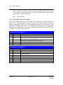
TABLE OF CONTENTS
1
INTRODUCTION..................................................................................................... 1
1.1
1.2
1.3
1.4
2
GENERAL ............................................................................................................. 1
LUMISTAR UNIVERSAL DAUGHTERBOARD FAMILY ............................................. 2
MANUAL FORMAT AND CONVENTIONS ................................................................ 2
SPECIFICATIONS ................................................................................................... 4
INSTALLATION ...................................................................................................... 6
2.1
ADDRESSING ........................................................................................................ 6
2.1.1
PCI Cards ................................................................................................... 6
2.1.2
VME Cards.................................................................................................. 6
2.2
PHYSICAL INSTALLATION .................................................................................... 7
2.3
INDICATORS ......................................................................................................... 7
2.4
INTERFACE ........................................................................................................... 8
2.5
PARALLEL OUTPUT ............................................................................................ 16
2.6
NOTES ON SHUNTS AND SIGNAL NAMES ............................................................ 18
3
OPERATION OF THE LS-50-P WITH THE LDPS SOFTWARE .................. 21
3.1
CONFIGURING THE LS-50-P HARDWARE........................................................... 23
3.1.1
The LS-50-P Decommutator Tab .............................................................. 25
3.1.1.1 Major Frame Configuration .................................................................. 26
3.1.1.2 Minor Frame Configuration .................................................................. 29
3.1.1.3 Frame Synchronization Pattern ............................................................. 31
3.1.1.4 Frame Sync Sensitivity Parameters ...................................................... 33
3.1.1.5 Data Source Configuration ................................................................... 35
3.1.1.6 Decom Mode Check Boxs .................................................................... 37
3.1.1.7 Decom Status Displays ......................................................................... 38
3.1.1.8 Decommutator Word Attributes ........................................................... 39
3.1.1.9 Load Decom Button .............................................................................. 42
3.1.1.10
Saving the Decommutator Setup Configuration ............................... 42
3.1.2
The LS-50-P Simulator Tab ...................................................................... 43
3.1.2.1 Major Frame Configuration .................................................................. 44
3.1.2.2 Minor Frame Configuration .................................................................. 45
3.1.2.3 Frame Synchronization Pattern ............................................................. 46
3.1.2.4 Clock & Data Output Mode Configuration .......................................... 47
3.1.2.5 Status Displays ...................................................................................... 49
3.1.2.6 Dynamic Words Setup .......................................................................... 50
3.1.2.7 Unique Words Setup ............................................................................. 50
3.1.2.8 Simulator Word Attributes.................................................................... 51
3.1.2.9 Load Simulator Button.......................................................................... 52
3.1.2.10
Saving the Simulator Setup Configuration ....................................... 53
3.1.3
The LS-50 Bit Synchronizer Tab ............................................................... 54
3.1.3.1 Input Bit Rate ........................................................................................ 56
3.1.3.2 Input Source .......................................................................................... 56
3.1.3.3 Input Code ............................................................................................. 56
U610101
Lumistar, Inc.
Page iii
8/14/2006
LS-50 User’s Manual
3.1.3.4 Loop Bandwidth.................................................................................... 57
3.1.3.5 Use Filter ............................................................................................... 57
3.1.3.6 Output Code .......................................................................................... 57
3.1.3.7 Bit Sync Status Display ........................................................................ 57
3.1.3.8 Load Bit Sync Button............................................................................ 57
3.1.3.9 View Extended Functions ..................................................................... 58
3.1.3.10
Saving the Bit Synchronizer Setup Configuration ............................ 59
3.1.4
The LS-50 IRIG Time Code Tab ............................................................... 60
3.1.4.1 IRIG Time Code Reader Menu ............................................................. 61
3.1.4.2 IRIG Time Code Generator Menus....................................................... 62
3.1.4.3 Bit Sync Status Display ........................................................................ 63
3.1.4.4 Load IRIG Button ................................................................................. 63
3.1.4.5 Saving the IRIG Time Code Setup Configuration ................................ 63
3.1.5
LS-50 Bit Error Rate Test (BERT) Function............................................. 65
3.1.5.1 BERT Configuration Setup Menu ........................................................ 67
3.1.5.2 BER Strip Chart Configuration ............................................................. 69
3.1.5.3 Data Results Display ............................................................................. 70
3.1.5.4 History Display ..................................................................................... 71
3.1.6
The LS-50-P Standalone Application........................................................ 73
4
PROGRAMMING INFORMATION ................................................................... 76
4.1
GENERAL ........................................................................................................... 76
4.2
LOCATING A PCI DEVICE ................................................................................... 76
4.3
VME ADDRESSING ............................................................................................ 78
4.4
REGISTER SUMMARIES ....................................................................................... 78
4.5
GENERAL REGISTERS ......................................................................................... 82
4.5.1
Board ID Register ..................................................................................... 82
4.5.2
Identifier Register ..................................................................................... 82
4.5.3
The Control Register ................................................................................. 83
4.5.4
Selecting the Input Source ........................................................................ 83
4.5.5
The Frame Sync Pattern ........................................................................... 84
4.5.6 The Decommutator Format Memory ................................................................. 86
4.5.7
Major Frame Synchronization .................................................................. 87
4.5.7.1 SFID Correlation................................................................................... 88
4.5.7.2 FCC Correlation .................................................................................... 89
4.5.7.3 URC Correlation ................................................................................... 89
4.5.8
The Decommutator Output ....................................................................... 90
4.5.9
Status ......................................................................................................... 91
4.6
THE IRIG TIME READER .................................................................................... 94
4.6.1
Setting the Real Time Clock ...................................................................... 94
4.6.2
Reading Time ............................................................................................ 95
4.7
THE PCM SIMULATOR ....................................................................................... 95
4.7.1
Simulator Command Register and Mode Registers .................................. 96
4.7.2
Output Formatting .................................................................................... 98
4.7.3
The Clock Generator............................................................................... 100
4.7.4
Communicating With Simulator Memory ............................................... 101
4.7.5
The Simulator Memory Map ................................................................... 102
U610101
Lumistar, Inc.
Page iv
8/14/2006
LS-50 User’s Manual
4.7.6
Attributes and Data ................................................................................. 102
4.8
THE IRIG TIME GENERATOR ........................................................................... 103
4.9
INTERRUPTS ..................................................................................................... 104
4.9.1
Polling ..................................................................................................... 104
4.9.2
Using PCI Interrupts............................................................................... 105
4.9.2.1 Connecting to the System ................................................................... 105
4.9.2.2 Preparing to be Interrupted ................................................................. 105
4.9.2.3 Being Interrupted ................................................................................ 106
4.9.3
Using VME Interrupts ............................................................................. 107
4.10 PCI DMA ........................................................................................................ 107
4.10.1
DMA Descriptors .................................................................................... 108
4.10.2
DMA Channel Mode Register ................................................................. 109
4.10.3
DMA Channel Command Register.......................................................... 109
4.11 TUNABLE BIT SYNCHRONIZER MODULE .......................................................... 110
4.12 BIT ERROR RATE MEASUREMENT .................................................................... 111
U610101
Lumistar, Inc.
Page v
8/14/2006
LS-50 User’s Manual
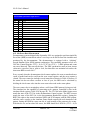
List of Tables
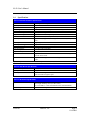
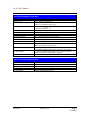
Table 1-1 PCM Decommutator Specifications ................................................................... 4
Table 1-2 Time Reader Specifications................................................................................ 4
Table 1-3 Mechanical Specifications .................................................................................. 4
Table 1-4 PCM Simulator Specifications ........................................................................... 5
Table 1-5 Environmental Specifications............................................................................. 5
Table 2-1 VME Address Switch Settings ........................................................................... 7
Table 2-2 VME Interrupt Switch Settings .......................................................................... 7
Table 2-3 Parallel Output Pinout ...................................................................................... 18
Table 2-4 CompactPCI P2 I/O Connector Pinout ............................................................. 19
Table 2-5 PMC Pinout ...................................................................................................... 20
Table 3-1 LS-40-DB Supported PCM Input Codes (normal or inverted) ........................ 56
Table 3-2 LS-40-DB Supported PCM Output Codes ....................................................... 57
Table 4-1 PCM Decom Write Register Summary ............................................................ 79
Table 4-2 PCM Decom Read Register Summary ............................................................. 80
Table 4-3 PCM Simulator Write Register Summary ........................................................ 80
Table 4-4 PCM Simulator Read Register Summary ......................................................... 81
Table 4-5 IRIG Generator Write Register Summary ........................................................ 81
Table 4-6 IRIG Generator Read Register Summary ......................................................... 81
Table 4-7 IRIG Reader Write Register Summary............................................................. 82
Table 4-8 IRIG Reader Read Register Summary ............................................................. 82
Table 4-9 Control Register................................................................................................ 84
Table 4-10 Source Control Register ................................................................................. 85
Table 4-11 Polarity Control Register ................................................................................ 86
Table 4-12 Decommutator Attribute Word....................................................................... 87
Table 4-13 Major Frame Sync Control Register ............................................................... 90
Table 4-14 Frame Header ................................................................................................. 91
Table 4-15 Buffer Control and Status Register................................................................. 92
Table 4-16 Status Register ................................................................................................ 93
Table 4-17 Header Register .............................................................................................. 93
Table 4-18 IRIG Reader Control Register ........................................................................ 95
Table 4-19 Simulator Command Register ........................................................................ 97
Table 4-20 Simulator Mode Register ................................................................................ 98
Table 4-21 Simulator Frame Start Register ...................................................................... 99
Table 4-22 Simulator Encoder Control Register .............................................................. 99
Table 4-23 Simulator Bankswitch Register .................................................................... 101
Table 4-24 Simulator Memory Map ............................................................................... 102
Table 4-25 Simulator Word Attributes ........................................................................... 103
Table 4-26 Simulator Frame Attributes .......................................................................... 103
Table 4-27 IRIG Generator Control Register ................................................................. 104
Table 4-28 Bit Sync Control Register ............................................................................. 110
Table 4-29 Bit Sync Status Register ............................................................................... 110
Table 4-30 Bit Synchronizer Input Source ..................................................................... 111
Table 4-31 Error Count High Register............................................................................ 112
U610101
Lumistar, Inc.
Page vi
8/14/2006
LS-50 User’s Manual
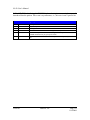
List of Figures
Figure 2-1 Front Plates........................................................................................................ 9
Figure 2-2 LS-50-PCI Card (Component Side) ................................................................ 10
Figure 2-3 LS-50-V Card (Component Side) ................................................................... 11
Figure 2-4 LS-50-cPCI Card (Component Side) .............................................................. 12
Figure 2-5 LS-50 J1 to E1 Patch Header Pin Assignment Chart ...................................... 14
Figure 2-6 LS-50 J1 to E2 Patch Header Pin Assignment Chart ...................................... 15
Figure 2-7 LS-50 Pigtail Connector Assembly (Single-Ended Signals) .......................... 16
Figure 2-8 LS-50 Pigtail Connector Assembly (Differential Signals).............................. 17
Figure 3-1 LDPS Status Display for the LS-50 ............................................................... 21
Figure 3-2 LDPS Server Application Windows ............................................................... 22
Figure 3-3 Configuration Menus/Controls for the LS-50-P ............................................. 23
Figure 3-4 The LS-50-P Decom Tab Configuration Menus ............................................. 25
Figure 3-5 Unique Recycle Code Variation of the Decom Setup Tab ............................. 31
Figure 3-6 LS-50 Decom – Word Attributes Setup .......................................................... 39
Figure 3-7 The LS-50-P Simulator Configuration Menus ................................................ 43
Figure 3-8 PCM Code Definitions .................................................................................... 48
Figure 3-9 Some Examples of Convolutional Encoder Circuits ....................................... 49
Figure 3-10 LS-50 Simulator – Word Attributes Setup .................................................... 51
Figure 3-11 The LS-50 Bit Synchronizer Configuration Menus ...................................... 54
Figure 3-12 Bit Synchronizer Extended Functions Display ............................................. 58
Figure 3-13 The LS-50 IRIG Time Code Reader/Generator Configuration Menus ......... 60
Figure 3-14 Configuration Menus/Controls for the LS-50-P BERT Functionality .......... 65
Figure 3-15 BER Strip Chart Recorder Display ............................................................... 70
Figure 3-16 BER Data Results Display ............................................................................ 71
Figure 3-17 BER History Display..................................................................................... 71
Figure 3-18 LS-50-P Standalone Application Window .................................................... 73
Figure 3-19 Major Frame Status Display.......................................................................... 74
Figure 3-20 Frame Dump Display Window ..................................................................... 75
U610101
Lumistar, Inc.
Page vii
8/14/2006
LS-50 User’s Manual
1
Introduction
1.1 General
This document presents information about the VME,
cPCI, and PCI form factors of the Lumistar LS-50
Multi-function PCM Decommutator and it’s
companion daughterboards. The Lumistar LS-50
Multi-function PCM Decommutators offer the latest
in flexibility by using a “Universal Daughterboard”
concept that allows the user to Lumistar LS-50-P
select 5 functions to be achieved in a single card slot. The user can
also select a second LS-55-DB decommutator daughtercard in
addition to the simulator, decommutator, and IRIG Time Code
Reader and Generator on the main board. The LS-55-DB
daughtercard decommutator, or an external decommutator can be
connected to process an embedded PCM data stream in accordance
with IRIG-106. Or, the LS-55-DB daughtercard decommutator can
be used for a second independent PCM data stream.
Lumistar LS-55-DB
Along with the Universal Daughtercard slot, the LS-50-P PCI decommutators can
simultaneously accommodate a Lumistar LS-40-DB Tunable PCM Bit Synchronizer
module. The LS-50-V VME decommutator can accommodate one or the other.
Lumistar LS-50-V
Lumistar LS-50-cPCI
The Lumistar LS-50 decommutator can be used for extremely large frame formats
(16,383 words per minor frame up to 1,024 frames deep) and contains dual ping-pong
data output buffers, each with 128K bytes of memory. The LS-50 decommutator includes
U610101
Lumistar, Inc.
Page 1
8/14/2006
LS-50 User’s Manual
a time code reader to insert timestamp information into the buffered data. The time reader
can be preset to local time and free-run, or accept an IRIG A, B, or G time carrier input.
The LS-50 decommutator system includes a dynamic and flexible PCM simulator that
can generate common, unique, and waveform pattern data words. The simulator also
includes a time signal generator that can be preset to local time and provides an IRIG A,
B, or G output signal.
1.2 Lumistar Universal Daughterboard Family
The LS-50 decommutator may be equipped with one of a family of optional
daughtercards to add functionality. Current options include:
Tunable Bit Synchronizer
Second Decommutator
Lumistar LS-40-DB Bit Synchronizer
1.3
Lumistar LS-55-DB Decommutator
Manual Format and Conventions
This manual contains the following sections:
Chapter 1 provides a brief product overview and technical specifications
Chapter 2 provides installation and configuration instructions
Chapter 3 provides info on the LS-50-P LDPS software
Chapter 4 provides programming information
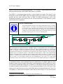
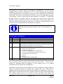
Throughout this document, several document flags will be utilized to emphasis warnings
or other important data. These flags come in three different formats: Warnings,
Cautions, and Information. Examples of these flags appear below.
U610101
Lumistar, Inc.
Page 2
8/14/2006
LS-50 User’s Manual
U610101
Lumistar, Inc.
Page 3
8/14/2006
LS-50 User’s Manual
1.4
Specifications
Table 1-1 PCM Decommutator Specifications
Input Data Rate
Input Signals
Input Levels
Word Length
CRC checker
Minor Frame Length
Major Frame Length
Bit Order
Frame Sync Pattern
Frame Sync Location
Frame Sync Strategy
Sync Error Tolerance
Sync Slip Window
Data Polarity
Major Frame Sync
URC Location
SFID Location
System Output
<100.0 bps to 20.0 Mbps
NRZ-L data & 0 clock
Single-ended TTL & RS-422
Variable from 3 to 16 bits per word on a word-by-word basis
CRC16/CCITT
2 to 16,383 words per minor frame
Up to 1024 minor frames per major frame
MSB or LSB-first (word-by-word basis)
Up to 64 bits (any pattern, including “don’t care" bits (X) may be
used)
Beginning or end of the frame
Adaptive mode (search-lock-verify) & burst mode (search-lock)
0 to 15 bits (selectable)
1 or 3 bits wide (selectable)
Normal, inverted or automatic
FCC (FAC), SFID or URC
Any 32 bit window within the first minor frame not including the last
bit in the minor frame
Any series of contiguous bits not including the last bit in the minor
frame
Buffered output with status, time, & data
Table 1-2 Time Reader Specifications
Time Reader Input Format
Input signal level
Data Outputs
IRIG A, B, or G
1 v p-p nominal
Automatic time tags for PCM data blocks
Time accessible in register space
Table 1-3 Mechanical Specifications
Form Factors
Power Dissipation
U610101
3U x160 CompactPCI
Full-Length “Desktop” PCI (2.2 M33, D32)
6U x 160 VME (C.2 A24/A32 D08/D16/D32, D16/D32 Block)
4 watts without daughtercard
Lumistar, Inc.
Page 4
8/14/2006
LS-50 User’s Manual
Table 1-4 PCM Simulator Specifications
Outputs
Output Levels
Output Data Rate
PCM Codes
Word Length
CRC Generator
Minor Frame Length
Major Frame Length
Bit Order
Frame Sync Pattern
Major Frame Sync
Common Words
Unique Words
Waveform Words
Time Generator Output
NRZ-L and PCM Data, 0-degree clock & minor frame strobes
Single-ended TTL & RS-422
64 bps to 20.0 Mbps (NRZ codes)
64 bps to 10.0 Mbps (all other codes)
NRZ-L/M/S; Bi-L/M/S; DM-M/S; M2, RNRZ-L-11/15, k=7
Convolutional Rate 1/2, 1/3
Variable from 3 to 16 bits per word on a word-by-word basis
CRC16/CCITT
2 to 16,384 words per minor frame
Up to 1024 minor frames per major frame
MSB or LSB-first
Up to 256 words (any series of 0s or is 1s may be used)
FCC (FAC), SFID
May be a single value or selected from a group of one minor frame.
Data may be changed while operating.
Seven may be programmed in any mainframe, super-commutated, or
subcommutated channel. Data may be changed while operating.
Five may be programmed to appear in every frame at the same
location. Data may be changed while operating.
IRIG A, B, or G
Table 1-5 Environmental Specifications
Temperature (Operating)
Temperature (Non-Operating)
Humidity (Operating)
Humidity (Non-Op)
Special Handling
U610101
0 to 50 oC
-25 to +70 oC
10% to 90% Non-Condensing
Packaging must prevent contact with moisture and contaminants
Standard ESD methods required
Lumistar, Inc.
Page 5
8/14/2006
LS-50 User’s Manual
2
Installation
2.1 Addressing
2.1.1 PCI Cards
(This paragraph Refers to both PCI and CompactPCI
form factors.) The LS-50 decommutator occupies both
PCI I/O space and memory space. No address switch is
used, as the address is determined by the system. 128
bytes of I/O space are always occupied. The card will
respond to any access in its I/O space. The first 64 bytes
of that space are assigned to the decommutator, and Lumistar LS-50-P
accesses to the first byte will return an ASCII identifier string. If a daughtercard of any type
is present, it will respond with its own identifier string offset 64 bytes up from the base
address of the card. The LS-50-PCI card is shown in Figure 2-2 on page 10. The LS-50-cPCI
card is shown in Figure 2-4 on page 12.
The amount of memory space taken up by the LS-50
is circumstantial. If a LS-55-DB decommutator is also
present, then twice as much space will be occupied
and the upper half of that space will access the second
decommutator. The other factor is the memory
addressing mode recognized by the buffer memory.
PCI cards are normally shipped in a “flat” addressing
mode wherein the 128 Kbyte buffer memory is
mapped one-to-one into PCI memory space. The
Lumistar LS-50-cPCI
configuration can be changed to activate a bankswitch
register in the decommutator(s) and maps the selected bank into 16Kbytes of MS-DOS real
memory space. The user’s computing environment may not allow for the use of this mode,
but Lumistar uses it for testing purposes. In either case, if a LS-55-DB decommutator is
present, it will map either 128K or 16K higher in system memory space.
2.1.2 VME Cards
The LS-50-V VME decommutator (see Figure 2-3 on page 11) operates at
a VME address and occupies address space according to address switch
settings. The LS-50-V VME card may be in VME Standard or Extended
Space, and may be in a “paged” or “flat” addressing mode similar to the
PCI form factors. A VME card set for flat mode occupies 512 Kbytes of
address space. A card set for page mode occupies 64 Kbytes. VME
addressing is controlled by three DIP switches S1, S3, and S4. They must
be set to the desired space, address, and mode as shown in Table 2-1 on
page 7.
Lumistar LS-50-V
The user must also choose a VME interrupt level and set DIP switch S2 accordingly. Settings
other than those in Table 2-2 on page 7 are apt to cause spurious interrupt crashes.
U610101
Lumistar, Inc.
Page 6
8/14/2006
LS-50 User’s Manual
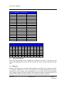
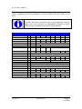
Table 2-1 VME Address Switch Settings
Switch
S1-1
S1-2
S1-3
S1-4
S1-5
S1-6
S1-7
S1-8
S3-1
S3-2
S3-3
S3-4
S3-5
S3-6
S3-7
S3-8
S4-1..3
S4-4..7
S4-8
On
A24 = 0
A25 = 0
A26 = 0
A27 = 0
A28 = 0
A29 = 0
A30 = 0
A31 = 0
A16 = 0
A17 = 0
A18 = 0
A19 = 0
A20 = 0
A21 = 0
A22 = 0
A23 = 0
Flat Mode
Page Mode
VME Extended
Off
A24 = 1
A25 = 1
A26 = 1
A27 = 1
A28 = 1
A29 = 1
A30 = 1
A31 = 1
A16 = 1
A17 = 1
A18 = 1
A19 = 1
A20 = 1
A21 = 1
A22 = 1
A23 = 1
Page Mode
Flat Mode
VME Standard
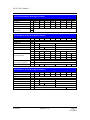
Table 2-2 VME Interrupt Switch Settings
IRQ
1
2
3
4
5
6
7
S2-1 S2-2 S2-3 S2-4 S2-5 S2-6 S2-7 S2-8 S2-9
On
Off Off Off Off Off Off Off
On
Off
On
Off Off Off Off Off
On
Off
Off Off
On
Off Off Off Off Off Off
Off Off Off
On
Off Off Off
On
On
Off Off Off Off
On
Off Off Off
On
Off Off Off Off Off
On
Off
On
Off
Off Off Off Off Off Off
On
Off Off
S2-10
On
On
On
Off
Off
Off
Off
2.2 Physical Installation
The LS-50 decommutator can be installed in any physical slot where it fits. Remove and
discard the blanking plate from the chosen slot (save the screw(s)!) and carefully insert the
card.
2.3 Indicators
Multiple LED indicators are provided. These indicators are in three rows, as shown in Figure
2-1 on page 9. Indicators [1..3] on the LS-50-cPCI are the board ID indicators. These are
connected to a static register and are intended for use by device drivers in environments
where multiple cards are present to identify which board is assigned to which data stream. On
desktop PCI and VME cards these indicators are chip LEDs on the board surface.
U610101
Lumistar, Inc.
Page 7
8/14/2006
LS-50 User’s Manual
Indicators [4..5] on the LS-50-cPCI are controlled by the decommutator. Indicator 4 is a
minor frame lock indication. Indicator 5 is a major frame lock indication. Indicator 6 lights
when the IRIG time reader detects a valid IRIG time carrier.
Indicators [7..9] on all LS-50 variants are used only if a daughtercard is present. If the
daughtercard is a second decommutator, these are assigned to the daughtercard to be used in
the same manner is indicators [4..6]. If a daughtercard of some other type is present, these
indicators will have meaning as defined by the daughtercard.
2.4 Interface
The LS-50 decommutator uses a 44-position female high density subminiature “DB” type
connector designated J1 for I/O. This connector has three rows of pins. The first row of pins
is primarily for use by the decommutator. The second row is primarily ground pins, and the
third row is reserved for use by whatever daughtercard is installed, if any. Pin assignments
are shown in Figure 2-5 on page15. If a Bit Synchronizer module or daughtercard is installed,
pinouts are as shown in Figure 2-6 on page 15 and apply for pins [31..44.]
Fourteen pins are assigned to the (each) decommutator for general-purpose I/O. The pinout is
limited by the number of physical I/O pins that can be accommodated by the plate. There are
possibilities for other I/O’s than the default assignments. Hence the decommutator has a
patch array E1 located at the front edge of the card immediately behind the I/O connector.
The LS-50 products are shipped with two mating pigtail cables to interface with the 44position J1 connector. The differential signal version of the cable is documented in figure
Figure 2-7 on page 16. The single-ended signal version is documented in figure Figure 2-8 on
page 17.
U610101
Lumistar, Inc.
Page 8
8/14/2006
LS-50 User’s Manual
LS50 PCI Front Panel Indicators
LS50 VME Front Panel Indicators
LS50 3U cPCI Front Panel Indicators
LED 4 Decom Min. Frame Lock
LED 5 Decom Maj. Frame Lock
LED 7 DB Decom Min. Frm Lck
LED 6 IRIG Signal Present
LED 8 DB Decom Maj. Frm Lck
LED 9 DB IRIG Signal Pres.
LED 9 Bit Sync Sig Qual
LED 8 Bit Sync PLL Lock
44
30
15
LED 7 Bit Sync Signal Threshold
44
30
15
LED 4 Decom Min. Frame Lock
LED 5 Decom Maj. Frame Lock
LED 6 IRIG Signal Present
1
16
31
LED 4 Decom Min. Frame Lock
LED 9 Bit Sync Sig Qual
LED 5 Decom Maj. Frame Lock
1
16
31
LED 6 IRIG Signal Present
LED 8 Bit Sync PLL Lock
LED 7 Bit Sync Signal Threshold
LED 3 PCI ID Bit 3
44
30
15
LED 2 PCI ID Bit 2
LED 1 PCI ID Bit 1
1
16
31
Figure 2-1 Front Plates.
U610101
Lumistar, Inc.
Page 9
8/14/2006
LS-50 User’s Manual
Figure 2-2 LS-50-PCI Card (Component Side)
U610101
Lumistar, Inc.
Page 10
8/14/2006
LS-50 User’s Manual
Figure 2-3 LS-50-V Card (Component Side)
U610101
Lumistar, Inc.
Page 11
8/14/2006
LS-50 User’s Manual
Figure 2-4 LS-50-cPCI Card (Component Side)
U610101
Lumistar, Inc.
Page 12
8/14/2006
LS-50 User’s Manual
LS-50 Decommutator systems are normally shipped with fifteen pin-pairs shunted together
as shown (Default) in Figure 2-5 on page 14. If the user’s application needs any of the signals
on E1 pins [29..48], then it will be necessary to sacrifice some of the existing I/O’s by pulling
the corresponding shunts, and wire-wrapping E1 pins to establish the desired pinout. Outputs
14 and 15 appear on E1. If these are to be used, the user will have to disable some of the
default patching to find homes for them on J1.
If no daughtercard occupies it, the 2mm header EA2 (near the 44-pin connector) needs shunts
at pins 7-8, 9-10, and 11-12 to activate the bit synchronizer clock and data outputs. See
Figure 2-6 on page 15 for more details on this.
Patch array E7 provides two 100-ohm terminations from the selected bit synchronizer
input(s) to ground. When single-ended inputs are used, the input termination on the bit
synchronizer module itself (selected by JP2) is connected directly to the selected input. When
a differential input is selected, that termination is isolated from the input and a termination
from E7 can be used. By convention, boards are shipped with shunts deliberately missinstalled (a pin off) on E7.
On VME boards an additional header J5 is placed next to J2 (see Figure 2-3 on page 11).
Odd-numbered J5 pins [1..39] connect to VME pins P2c2..P2c21. Even-numbered J5 pins
[2..40] connect to VME pins P2a2..P2a21. Individual J5 pins can be wire-wrapped to E1 pins
to move front-plate signals to P2.
The LS-50-cPCI card shown in Figure 2-4 on page 12 also presents the front plate signals
and others at the compactPCI P2 connector. P2 is normally not populated. If the board is
configured with P2, it will present the signals shown in Table 2-4 on page 19 at P2.
U610101
Lumistar, Inc.
Page 13
8/14/2006
LS-50 User’s Manual
Figure 2-5 LS-50 J1 to E1 Patch Header Pin Assignment Chart
U610101
Lumistar, Inc.
Page 14
8/14/2006
LS-50 User’s Manual
Figure 2-6 LS-50 J1 to E2 Patch Header Pin Assignment Chart
U610101
Lumistar, Inc.
Page 15
8/14/2006
LS-50 User’s Manual
Figure 2-7 LS-50 Pigtail Connector Assembly (Single-Ended Signals)
2.5 Parallel Output
The LS-50 decommutator also provides a parallel output port. This output appears at header
EA3, and also on header J2 in the PCI and VME form factors. Header EA3 is a 2mm 40-pin
male header. J2 is a 0.1-inch 40-pin header. These headers have the same pinout shown in
Table 2-3 on page 18.
On LS-50 VME boards, an additional header J5 is placed next to J2. Odd-numbered J5 pins
[1..39] connect to VME pins P2c2..P2c21. Even-numbered J5 pins [2..40] connect to VME
pins P2a2..P2a21. If J5 is connected to J2 by a short ribbon-cable jumper, the parallel output
appears on P2. Or individual J5 pins can be wire-wrapped to E1 pins to move front-plate
signals to P2 (grounds can be picked up at even-numbered pins [20..40] of J2.)
U610101
Lumistar, Inc.
Page 16
8/14/2006
LS-50 User’s Manual
Figure 2-8 LS-50 Pigtail Connector Assembly (Differential Signals)
U610101
Lumistar, Inc.
Page 17
8/14/2006
LS-50 User’s Manual
Table 2-3 Parallel Output Pinout
J2 Pin
1
3
5
7
9
11
13
15
17
19
21
23
25
27
29
31
33
35
37
39
Signal
Ground
OD1
OD2
OD3
OD4
OD5
OD6
OD7
OD8
Ground
WdStb
FrmStb
MFStb
Clock
1stBIT
Lock
MFLock
Ground
Ground
Ground
J2 Pin
2
4
6
8
10
12
14
16
18
20
22
24
26
28
30
32
34
36
38
40
Signal
Ground
OD9
OD10
OD11
OD12
OD13
OD14
OD15
OD16
Ground
Ground
Ground
Ground
Ground
Ground
Ground
Ground
Ground
Ground
Ground
2.6 Notes on Shunts and Signal Names
The “Default” shunt locations documented in Figure 2-5 on page 14 show where shunts are
normally installed at the factory.
The J1 pins [01..14] are merely clad tracks connecting E1 and J1. Their meaning is strictly a
function of how E1 is patched. The J1 pins [31..44] are similarly flexible in meaning and are
based on the daughtercard installed. If the daughtercard is a second decommutator, then J1
pins [31..44] will be a function of how the similar E1 header on the daughtercard is patched.
Figure 2-6 on page 15 documents the “Default” shunt locations on EA2.
For the decommutator inputs in Table 2-5 on page 20 that have a bracketed number attached,
it indicates those signals have meaning only when the decommutator Source Control register
source select field has the bracketed value. Otherwise they are ignored.
The simulator baseband output is a bipolar signal. It is a simulator PCM data representation
and swings approximately 2 volts peak-to-peak open-circuit, and approximately 1 volt
peak-to-peak when loaded by 75 ohms. The IRIG Time carrier input and output are
nominally 1 volt peak-to-peak at low level, and 3.3 volts peak-to-peak at high level. The
input impedance of the IRIG Time input is nominally 100 ohms with the termination at E149 present, and 5K ohms when it is removed. Logic-type inputs are compatible with TTL
levels and are terminated into approximately 130 ohms at 3 VDC. Differential signals are
U610101
Lumistar, Inc.
Page 18
8/14/2006
LS-50 User’s Manual
indicated by a trailing polarity + or − character. Differential outputs are capable of driving
RS-422 or TTL-compatible inputs. Differential inputs are pulled slightly asymmetrically to
float to a data “0” state when un-driven. They may be driven by single-ended TTL signals by
leaving the “−” end unconnected, albeit at some loss of noise immunity.
Table 2-4 CompactPCI P2 I/O Connector Pinout
Pin
1
2
3
4
5
6
7
8
9
10
11
12
13
14
15
16
17
18
19
20
21
22
Row A
Ground
OD1
OD2
OD3
OD4
OD5
OD6
OD7
OD8
Ground
WdStb
FrmStb
MFStb
Clock
1stBIT
Lock
MFLock
Ground
Ground
Ground
n/c
n/c
Row B
Ground
OD9
OD10
OD11
OD12
OD13
OD14
OD15
OD16
Ground
Ground
Ground
Ground
Ground
Ground
Ground
Ground
Ground
Ground
Ground
n/c
n/c
Row C
n/c
2SP01
2SP02
2SP03
2SP04
2SP05
2SP06
2SP07
2SP08
2SP09
2SP10
2SP11
2SP12
2SP13
2SP14
2SP15
2SP16
n/c
n/c
n/c
n/c
n/c
Row D
Ground
Ground
Ground
Ground
Ground
Ground
Ground
Ground
Ground
Ground
Ground
Ground
Ground
Ground
Ground
Ground
Ground
Ground
Ground
Ground
n/c
n/c
Row E
n/c
1SP01
1SP02
1SP03
1SP04
1SP05
1SP06
1SP07
1SP08
1SP09
1SP10
1SP11
1SP12
1SP13
1SP14
n/c
n/c
n/c
n/c
n/c
n/c
n/c
Row F
Ground
Ground
Ground
Ground
Ground
Ground
Ground
Ground
Ground
Ground
Ground
Ground
Ground
Ground
Ground
Ground
Ground
Ground
Ground
Ground
Ground
Ground
The Sim IRIG Time DC Level Out signal in Table 2-5 is a demodulated representation of the
simulator IRIG Time carrier output.
The Sim Frame Strobe in Table 2-5 is a one-bit pulse coincident with the last bit of the
simulator minor frame.
The Force inputs in Table 2-5 are for use where the input data has no sync pattern. When set
up for this mode, the decommutator will expect the Force input to be high during the first bit
of the frame.
The Slave signals in Table 2-5 are for use when two decommutators and/or two simulators
are interconnected in reference to asynchronous embedded formats.
U610101
Lumistar, Inc.
Page 19
8/14/2006
LS-50 User’s Manual
The OD[1..16] signals are decommutator parallel output data. During the first bit time of a
word 1stBIT is high and the current minor frame number is right-aligned on OD[7..16]
(OD16 is the LSB.) During the remaining bit times, these lines are zero-extended parallel
data. This data is normally left-aligned (OD1 is the MSB) unless the decommutator is
programmed for right-aligned output. Lock and MFLock are active-high minor and major
frame lock status. WdStb rises one-half bit time after 1stBIT falls and lasts for one bit time.
The FrmStb and MFStb signals are high for the first word time of the minor and major
frames respectively.
Table 2-5 PMC Pinout
Pin
1
2
3
4
5
6
7
8
9
10
11
12
13
14
15
16
17
18
19
20
21
22
23
24
25
26
27
28
29
30
31
32
33
34
Signal
D Clock In[0]
Ground
D Data In[0]
Ground
D Status In[0]
Ground
D Force In[0]
Ground
D Slave Clock Out
Ground
D Slave Data Out
Ground
D Clock In[3]
Ground
D Data In[3]
Ground
D Clock In+[1]
D Clock In−[1]
Ground
Ground
D Data In+[1]
D Data In−[1]
Ground
Ground
D Force In+[1]
D Force In−[1]
Ground
Ground
D Status In[1]
Ground
T 1PPS Out
Ground
T Time In
Ground
U610101
Pin
35
36
37
38
39
40
41
42
43
44
45
46
47
48
49
50
51
52
53
54
55
56
57
58
59
60
61
62
63
64
65
66
67
68
Signal
S Clock Out+[7]
S Clock Out−
Ground
Ground
S NRZ-L Out+[7]
S NRZ-L Out−
S Frame Strobe+
S Frame Strobe−
Ground
Ground
S PCM Out+
S PCM Out−
Ground
Ground
S Baseband Out
Ground
S Slave Clk Out
Ground
S Slave Data In
Ground
S Ext Clock In
Ground
S Sym Clock Out+
S Sym Clock Out−
Ground
Ground
D Mezz Clk In[2]
D Mezz Data In[2]
T DC Level Out
Ground
D Mezz Status In[2]
Ground
S IRIG Time Out
Ground
Lumistar, Inc.
Page 20
8/14/2006
LS-50 User’s Manual
3
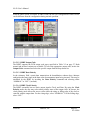
Operation of the LS-50-P With The LDPS Software
The LS-50-P PCI Multi-function PCM Decommutator
can be setup and controlled by using the Lumistar Data
Processing System (LDPS) software (shown below).
Note, the LS-50-V, and LS-50-cPCI are not currently
supported by the LDSP software.
The LDPS is composed of two major application
programs - the Server and the Client. The Server
program is used to setup and acquire data from
various sources (such as the LS-50-P). The
server archives the data, formats the data into a
normalized format, and then pass the data on to
the client application for further processing
and/or display. The Client is mainly a data
processing and presentation program, with hooks
to allow new display and processing routines to
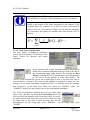
Figure 3-1 LDPS Status Display for
the LS-50
be added by the user. The server and client
applications can run together on the same
computing platform, or on different platforms interconnected via a Local Area Network
(LAN).
To initially configure the LS-50-P, perform the following steps:
1. Run the LDPS server program and from the System menu shown below, select
“Devices” and then “Manage” (System→ Devices→ Manage)
2. From the System Manager shown below left, select the “Enable” check box next to
the Ls50 button. The “Ls50_8x” button will then become active (not grayed out).
Note the red rectangle around the button - this indicates that the application has not
yet started. Note also the “Sim” check box next to the “Enable” check box. Checking
this box allows the LDPS application to operate when a LS-50-P board is not installed
in the system.
3. From the System Manager, click the “Ls50_8x” button. This will launch the
“Ls50_8x (Decom)” display shown below right. Note that the red rectangle around
the button has changed to green indicating that the application is now running.
4. To setup and configure the LS-50-P card, follow the procedures outlined in
paragraphs 3.1.
U610101
Lumistar, Inc.
Page 21
8/14/2006
LS-50 User’s Manual
Figure 3-2 LDPS Server Application Windows
U610101
Lumistar, Inc.
Page 22
8/14/2006
LS-50 User’s Manual
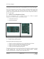
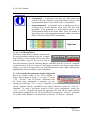
3.1 Configuring The LS-50-P Hardware
From the “Ls50_8x (Decom)” display1 shown below in Figure 3-3, click “Setup” and then
“Stream 1” (Setup →Stream 1).
Figure 3-3 Configuration Menus/Controls for the LS-50-P
The “LS-50 (Stream 1) Setup” display shown above in Figure 3-3 is divided into several
regions. Below the window header are the “File,” “Load All,” and “Set Defaults”
commands (more about these later). Each of the LS-50’s
four main functions have their own setup tab. To
completely configure the LS-50-P, visit each tab in turn
1
This figure shows the server setup window in “Simulation” mode, where the LS-50-P hardware is not installed
in the system. When actual LS-50-P hardware is installed, the server setup window appears as shown in Figure
3-14 on page 64
U610101
Lumistar, Inc.
Page 23
8/14/2006
LS-50 User’s Manual
and configure the functions. After the setup configuration is complete, save the settings by
invoking the “File → SaveAs” command. To download the configuration to the LS-50-P
hardware, invoke the “Load All” command. To recall a previously defined LS-50-P setup
configuration, invoke the “File → Recall” command and select the appropriate file from the
file menu and then download the configuration to the LS-50-P hardware by invoking the
“Load All” command.
To invoke the controls for any of the tabs in the display, simply place the mouse curser in a
region and right click. The resulting menus for the Decom tab are shown in Figure 3-4 on
page 25 and are discussed in detail in the following paragraphs. The configuration setup for
the Decommutator, Simulator, Bit Synchronizer, and IRIG Timecode functions are described
in detail as indicated in the table below.
See paragraph 3.1.1 on page 25 for
more info on the Decommutator.
See paragraph 3.1.2 on page 43 for
more info on the PCM Simulator.
See paragraph 3.1.3 on page 54 for
more info on the Bit Synchronizer.
See paragraph 3.1.4 on page 60 for
more info on the IRIG Timecode
Reader/Generator.
Each tab has a button control to load the setup information for the
portion of the card displayed with the tab. Changes made with any of
the controls will not take affect until this button is pressed.
There is also a window displayed (shown left) showing the status
of some of the LS-50’s functional states (like frame lock). This
status display is updated at a ten hertz rate. The user may load all
four major functions (Decom, Simulator, Bitsync, and IRIG) from
the “Load All” command on the menu next to the File menu). If
any changes are made to an individual setup without loading, a red
text will appear below the Load button (shown above right), indicating the displayed data
does not match the cards’ loaded data.
U610101
Lumistar, Inc.
Page 24
8/14/2006
LS-50 User’s Manual
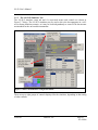
3.1.1 The LS-50-P Decommutator Tab
The LS-50-P decommutator setup tab and it’s associated menus and controls are shown in
Figure 3-4 below. There are up to seven groups of controls displayed for the decommutator,
depending on the setting of other controls. If a project is loaded from the LDPS server (see
Figure 3-2 on page 22), then some portions of the window will not be able to be controlled.
Figure 3-4 The LS-50-P Decom Tab Configuration Menus
U610101
Lumistar, Inc.
Page 25
8/14/2006
LS-50 User’s Manual
The seven control groups of the LS-50-P decom tab include:
1.
2.
3.
4.
5.
6.
7.
Major Frame Configuration
Minor Frame Configuration
Frame Synchronization Pattern (including optional URC)
Frame Sync Sensitivity Parameters
Data Source Configuration
Decommutator Modes
Word Attributes Control
Definitions:
Frame Synchronization Pattern – A unique binary bit pattern
used to indicate the beginning of a telemetry minor frame.
Frame Synchronizer – Correlator & State Machine circuitry that
recognizes unique bit patterns indicating the beginning of minor
frame data. The frame synchronizer typically “searches” for
patterns, “checks” for the recurrence of the pattern in the same
position for several frame periods, and then “locks” on the pattern.
3.1.1.1 Major Frame Configuration
The major frame configuration consists of five
controls/parameters that include: common word
length, the number of words per minor frame, the bit
order of the words in the frame, the frame
synchronization patter location, and the subframe
synchronization mode.
Definitions:
Major Frame – An integer number of minor frames, not to exceed
256 per the IRIG-106 specification. The LS-50 however can
support up to 1024 minor frames per major frame.
Minor Frame – A fixed length block of data sub-divided into an
integer number of fixed-length words. The LS-50 can support up
to 16,383 words per minor frame.
U610101
Lumistar, Inc.
Page 26
8/14/2006
LS-50 User’s Manual
The Common Word Length may be set from 3 to 16 bits in length.
The common word length defines the length in bits of the majority
of words that make up a minor frame. Note, not all words in a minor
frame need be of the same length. For example, the majority of the
words in a minor frame could be 8-bits in length, and thus the
common word length would be 8. However, several of the words
might be 14 or 16 bits in length and would be individually specified
using the Decommutator Word Attributes command function
described in paragraph 3.1.1.8 on page 39
The minor frame length is defined by the user by invoking
the Words Per Minor Frame command. Here, the user
enters the number of words (of length specified by word
attributes settings) that make up a minor frame. The minor
frame length on the LS-50 may be between 3 and 16,383
words.
By invoking the Bit Order command, the user specifies for the
common words of the minor frame whether the Most Significant
Bit (MSB) is first, as read from left to right, or the Least
Significant Bit (LSB) is first, again, read from left to right. Note,
not all words in a minor frame need have the same bit order. For example, the majority of the
words in a minor frame could have LSB first bit order. However, several of the words might
be MSB first and would be individually specified using the Decommutator Word Attributes
command function described in paragraph 3.1.1.8 on page 39
Note: The location of the frame synchronization pattern (FSP) may be
visualized, as in the examples here, as either being at the beginning of the
minor frame, or at the end. The location of the subframe identification
(SFID) word(s) is arbitrary.
U610101
Lumistar, Inc.
Page 27
8/14/2006
LS-50 User’s Manual
The user specifies the location of the FSP by invoking the FSP
Location command, and selecting “TRAILS” or “LEADS.”
To implement a subframe synchronization scheme, telemetry designers often add one or
more “special” words to each minor frame. These special words are used by the frame
synchronizer state machine to establish the location of the first minor frame in the major
frame. The LS-50 supports three subframe synchronization modes: SFID, FCC, and URC.
Definition:
SFID – The most commonly used subframe synchronization
method is called Subframe Identification (SFID).
In this method, the synchronization pattern occupies one or more words
in each minor frame. The SFID acts as a counter. The pattern value
increments or decrements to a specific value and then resets.
Definition:
FCC – Another commonly used subframe synchronization
method is called Frame Code Complement (FCC).
In this method, the complement (inverted) of the synchronization pattern
is placed in the FSP location in minor frame-0. All other FSPs are not
inverted. Because the complement of the frame synchronization pattern
exhibits the same correlation properties as the true pattern, frame sync
lock will not be compromised. Minimum sync overhead is attained using
this method, although it requires longer subframe acquisition time than
the SFID method.
U610101
Lumistar, Inc.
Page 28
8/14/2006
LS-50 User’s Manual
Definition:
URC – A less commonly used subframe synchronization method
is called Unique Recycle Code (URC).
URC is a slight variation on the FCC method. For URC, the beginning of
minor frame-0 is identified by a unique synchronization pattern NOT
related to the primary synchronization pattern.
The user specifies the method of subframe synchronization by
invoking the Subframe Mode command , and selecting “None,”
“SFID,” “FCC,” or “URC.” Note, if the user selects the “URC”
subframe synchronization mode, then a second frame
synchronization pattern setup area will appear on the Decom setup
tab as shown in Figure 3-5 on page 31.
3.1.1.2 Minor Frame Configuration
The minor frame configuration consists of five
controls/parameters that include: Minor Frame
Count Direction, Minor Frame Counts From,
Minor Frame Count, Sync ID Word Number, and
Sync ID MSB.
As mentioned previously, in the SFID mode, the
synchronization pattern occupies one or more
words in each minor frame and acts as a counter. The user may
specify whether the pattern value increments or decrements
from minor frame to minor frame by invoking the Minor
Frame Count Direction command, and selecting “UP,” or
“DOWN.”
U610101
Lumistar, Inc.
Page 29
8/14/2006
LS-50 User’s Manual
In some telemetry frame designs, the subframe counter in minor
frame-0 will initially begin counting from a starting value of zero
(0), while in other frame designs, the subframe counter will begin
counting from a starting value of one (1). The user specifies one or
the other of these two conditions by invoking the Minor Frame Counts From command.
As mentioned previously, the major frame is composed of an
integer number of minor frames, and the minor frame is a
fixed length block of data sub-divided into an integer number
of fixed-length words. By invoking the Minor Frame Count
command, the user may specify the number of minor frames
that make up the major frame. The LS-50 can support up to
1024 minor frames per major frame.
The location of the subframe identification (SFID) word(s) is
arbitrary within the minor frame and may be specified by the
user by invoking the Sync ID Word Number command. As
the LS-50 can support up to 16,383 words per minor frame,
the user may thus locate the SFID word anywhere within this
range, provided it does not overlap or coincide with the
frame synchronization pattern location.
As described previously, the SFID word is used as a counter, but
it is not always the case that ALL of the bits in the SFID word are
used for this purpose. For example, the SFID word might be
16-bits in length, but there might only be 512 minor frames in the
major frame. In this scenario, a 9-bit counter (29 = 512) would be
required and the user would specify the location of the counter
within the larger 16-bit word by invoking the Sync ID Msb
command and selecting the appropriate bit position for the most
significant bit of the SFID counter.
The Sync ID Msb is represented
graphically in the minor frame
configuration section as shown right.
U610101
Lumistar, Inc.
Page 30
8/14/2006
LS-50 User’s Manual
Figure 3-5 Unique Recycle Code Variation of the Decom Setup Tab
3.1.1.3 Frame Synchronization Pattern
The frame synchronization pattern parameters include:
the actual Pattern and the Pattern Length. The user may
enter the actual pattern in a variety of different format
representations including Hexadecimal (HEX), Binary
and Octal. If the synchronization pattern is to contain
“don’t care bits,” then the pattern must be entered in
binary As mentioned previously, the frame
synchronization pattern is a unique binary bit pattern used
to indicate the beginning of a telemetry minor frame. To achieve this, a frame synchronizer is
employed with correlator & state machine circuitry that recognizes unique bit patterns
indicating the beginning of minor frame data. The frame synchronizer typically “searches”
for patterns, “checks” for the recurrence of the pattern in the same position for several frame
periods, and then “locks” on the pattern.
U610101
Lumistar, Inc.
Page 31
8/14/2006
LS-50 User’s Manual
Definition:
Correlator – Logic circuit (see below) used to detect the presence
of a frame synchronization pattern used to identify the beginning of
a minor frame.
The synchronization strategy is to pass the incoming data stream into a
correlator which checks each bit of the input stream against a predefined
synchronization pattern. In the correlator, the data is passed through a shift
register, the contents of which are bitwise compared with the predefined
pattern once each bit period. When the summation output of the correlator
exceeds a preset threshold, the sync pattern is declared to have been found.
Optimal codes for the sync pattern are chosen because they have low
correlation unless the code pattern is exactly aligned with the desired
pattern.
To enter the required frame synchronization pattern, the user
must first invoke the Pattern Length command to specify
the bit length of the frame sync pattern. For the LS-50, the
length of the pattern may be up to 64-bits. After entering the
number of bits for the frame sync pattern, the appropriate
Barker code pattern will automatically be filled in on the
input pattern dialog box. This feature is based on the number of bits entered for the pattern
length (only for lengths of bits 7 through 32 bits will this occur). Then the user must select
one of the Hexadecimal (HEX), Binary or Octal format representation radio buttons. The
selected radio button will determine the appearance of the input pattern dialog box when the
Pattern command is invoked. Note that if the pattern length is NOT an even multiple of
eight (8), then the “Octal” radio button will be grayed out. Also, if the pattern length is not an
even multiple of four (4), then the “HEX” radio button will be grayed out.
U610101
Lumistar, Inc.
Page 32
8/14/2006
LS-50 User’s Manual
If the user wishes to use a pattern other than the one automatically selected based on the
pattern length, then the pattern command should be invoked and a different pattern should be
entered.
Note – Per the IRIG-106, it is recommended that for optimal results, the
frame synchronization pattern should be at least 16-bits in length2.
(24 or 32 bits would be much better). In the LS-50, the pattern may be up
to 64-bits in length
As previously mentioned, optimal codes for the sync pattern
should be chosen because they have low correlation properties
unless the code pattern is exactly aligned with the desired
pattern. To aid the user in selecting the appropriate pattern,
invoke the Barker Codes command for a convenient list of
some possible sync patterns. Note that choosing a pattern
form the popup list does not “enter” the pattern – that still
must be done via the Pattern command.
3.1.1.4 Frame Sync Sensitivity Parameters
The frame synchronization sensitivity parameters include: the
Sync Window and Sync Tolerance commands. Both of these
commands relate to how well the frame synchronization
process functions in a noisy, real world environment.
2
J. L. Maury, Jr. and J. Styles, "Development of Optimum Frame Synchronization Codes for Goddard Space
Flight Center PCM Telemetry Standards," in Proceedings of the National Telemetering Conference, June 1964.
U610101
Lumistar, Inc.
Page 33
8/14/2006
LS-50 User’s Manual
Statistical Measures – The primary performance measure used in
association with the frame synchronizer is; 1) the probability of falsely
locking onto a random data pattern and believing it to be the real sync
pattern, and 2) the probability of missing a valid sync pattern in the data
stream due to an unacceptable number of bit errors.
The probability of a false lock is only a function of the length of
the chosen sync pattern, and NOT a function of the channel biterror rate.
The probability of missing a valid pattern is a function of both
channel bit-error rate, and pattern length.
The frame synchronizer in the LS-50 typically “searches” for patterns,
“checks” for the recurrence of the pattern in the same position for several
frame periods, and then “locks” on the pattern. Because of certain
peculiarities in the demodulation and bit synchronization processes for
noisy channels, sometimes the recovered sync pattern may be shifted, or offset in time by one
or more bit time periods. If these “bit-slips” in the recovered sync pattern are not allowed and
accounted for, then the synchronization state machine will loose sync because the pattern is
NOT in the exact same position as it was in the previous minor frame. The user specifies the
number of bit-slips allowed by invoking the Sync Window command and entering a value of
up to 3 bits. Note, in a noisy signal environment, setting the window to Zero (0) would likely
result in the LS-50 NEVER acquiring or maintaining frame synchronization.
The user may specify the number of bits in the acquired sync pattern that
may be different from the ideal pattern and still achieve & maintain
synchronization by invoking the Sync Tolerance command. The user
may specify that the received pattern must contain no bit errors, and
would thus set the tolerance to Zero (0). In a noisy signal environment,
such a setting would likely result in the LS-50 NEVER acquiring or
maintaining frame synchronization. For the noisy, real world
environment, the user may set the bit error tolerance from 1 to 16 bits.
Some guidance on what to set the Sync Tolerance value to can be found
below.
U610101
Lumistar, Inc.
Page 34
8/14/2006
LS-50 User’s Manual
A “Geek” Technical Tidbit:
The probability of missing a valid sync pattern in a noisy environment….
The probability of missing a sync pattern in a data stream is directly
related to the number of bit errors encountered in the channel. If the
correlator allows for a number “k” or fewer bit errors (sync tolerance
value) to occur in a sync pattern of length “N” bits, then the probability
“P” of missing a sync pattern in a channel with a bit-error-rate of “B” is
given by:
P
N
j k 1
N!
j! N j !
B 1 B
j
N j
3.1.1.5 Data Source Configuration
The Data Source Configuration parameters
include: the Data Polarity, Clock Polarity, Data
Source, Frames Per Interrupt, and Output
Alignment.
In the telemetry field, certain data transmission & demodulation
schemes have inherent ambiguities that may result in the data at
the decommutator input being inverted. By invoking the Data
Polarity command, the LS-50 decommutator can be programmed
by the user to accept patterns of either data polarity. The
“AUTO” mode automatically inverts the incoming data if there is no frame lock and an
inverted pattern is detected. This mode should probably be defaulted to unless the sync
strategy is set to Frame Alternating Complement (FAC). To manually invert the incoming
data, irrespective of the frame sync status, one selects the “INVERT” mode. The
“NORMAL” mode leaves the polarity sense of the incoming data unchanged.
The LS-50 decommutator essentially has two basic signal input
types; Clock, and Data. By using the Clock Polarity mode, the
user may select either polarity sense of the input clock. In essence,
the clock polarity mode allows the user to select either the rising
or falling edge of the clock to latch incoming data into the
decommutator. For the rising edge, select “NORMAL.” For the falling edge, select
“INVERT.”
U610101
Lumistar, Inc.
Page 35
8/14/2006
LS-50 User’s Manual
The LS-50-P decommutator has five sets of data and clock
inputs, and the user may select from these by invoking the Data
Source command. The inputs that may be selected include: TTL,
RS-422, Slave, MEZZANINE, and SIMULATOR. For a singleended clock/data input, select “TTL.” For a differential
clock/data input, select RS-422. For applications involving an onboard LS-40 bit
synchronizer, select “MEZZANINE.” For applications involving embedded asynchronous
streams and an on-board LS-55-DB daughtercard decommutator, select “SLAVE.” For
development and testing applications, select “SIMULATOR.” This will allow the
decommutator to be driven by a known & controlled source of data. For more detailed
information on the nature of the TTL, RS-422, and Slave input clock/data signals, see
paragraph 2.4 on page 8.
The LS-50-P decommutator can be used with extremely
large frame formats (16,383 words per minor frame) and
contains dual ping-pong data output buffers, each with 128K
bytes of memory. The output of the decommutator is a
stream of words from the input, with a header prefixed to the
beginning of each minor frame. This data is grouped into
“blocks” of one or more minor frames and written to the on-board buffer memory. Two such
ping-pong buffers are provided. Normally while the decommutator writes to one ping-pong
buffer, the other is accessible for use. When a block’s worth of data has been written, an
interrupt is generated and the two buffers are logically switched so that fresh data becomes
available. The user may control the number of minor frames that make up the ping-pong
buffer by invoking the Frames Per Interrupt command. For optimal results, the user should
set the frames per interrupt value to some multiple of the minor frames per major frame size.
The LS-50 can support up to 256 frames per interrupt, depending on the frame size. Note, for
fast streams, the user should maximize the number of frames per interrupt to reduce the load
on the CPU. If the user is unsure what to set the frames per interrupt value to, the Set Max
FPI (Frames Per Interrupt) command may be invoked to set the maximum number of frames
per interrupt based on the minor frame size and the amount of memory on the card.
Note: The number of minor frames per interrupt cannot exceed:
a. 256
b. ((words-per-minor frame + 5) * 2 * frames per interrupt) cannot
exceed 131,072 bytes.
c. (words-per-minor frame + 5) cannot exceed 16,383 words.
U610101
Lumistar, Inc.
Page 36
8/14/2006
LS-50 User’s Manual
To select left-justified or right-justified output data from the
decommutator, the user may invoke the Output Alignment
command. Note: The output alignment should always be set to
Right Aligned, with the possible exception of connecting the LS-50
to a LS-71 DAC3. In general, if left alignment is selected, then the
processing overhead of LDPS will be increased, because part of the 'normalization' process
involves the right alignment of all the data prior to sending it off to the client or processing
tasks such as audio or video, etc.
Recommendation:
A good rule of thumb - If the minor frame rate is 50 Hz or less, then set
the FPI to 1. If it is more, then set it to the number of minor frames per
major frame, if it will fit. Otherwise the user will have to experiment with
FPI numbers between 1 and the minors-per-major (ideally a multiple of
minors-per-major).
3.1.1.6 Decom Mode Check Boxs
The LS-50 decommutator setup tab has a number of mode selection check
boxes that include: G Mode, External Sync, Raw Data Mode, Burst Mode,
Major Frame Mode, and FAC Enable.
Normally the decommutator output stops when it loses minor frame lock.
If G Mode is checked, the decommutator will continue to processes
incoming bits into “frames” and output them. If it detects a sync pattern while in this state, it
will abort the frame it is assembling, and start a new buffer. Basically, the G Mode tells the
decom to try to lock onto the frame sync pattern, but even if it cannot, it collects the buffer of
data and generates an interrupt even if there is no frame lock.
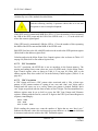
To support fixed length frames that arrive at irregular intervals, the user may check the Burst
Mode box. Check this box if the incoming data consists of fixed-length frames separated by
zero or more fill bits. The data in the frames will be output and the fill bits will be discarded.
3
If the bits-per-word is greater than 14, then left alignment may come into play as a possible requirement,
depending on what resolution the DAC output is using. If the data is right aligned and bits-per-word is 16, then
the two LSBs on the DAC output will be lost. If the data is left aligned, then the two MSBs on the DAC output
will be lost.
U610101
Lumistar, Inc.
Page 37
8/14/2006
LS-50 User’s Manual
Definition:
FAC – A less commonly used subframe synchronization method
that is a variant of the FCC mode is called Frame Alternating
Complement (FAC).
In this method, the frame synchronization pattern is alternated with the
complement of the frame synchronization pattern.
The Ext Sync mode instructs the decommutator to establish the “lock” condition based upon
an external sync pulse signal only. This mode bypasses the internal frame synchronizer
(correlator/state machine) in favor of an external signal provided by the user.
The Raw Data Mode instructs the decommutator to ignore the frame lock state (i.e., don’t
look for a frame sync pattern) and just ingest the correct number of bits and generate an
interrupt. This mode is used to record 100% of the input bits, regardless of lock state.
When selected, the Major Frame Mode will generate an interrupt only when a complete
major frame of data has been gathered and the decom is in major and minor frame lock.
Note, in this mode the frames per interrupt is fixed to the number of minor frames.
The FAC Enable mode is used to enable the Frame Alternating Complement subframe
synchronization method. As discussed above, the FAC mode is a variant of the FCC
subframe synchronization method.
3.1.1.7 Decom Status Displays
The LS-50-P decom setup tab has a window display showing the
status of some of the LS-50’s functional states. These states include:
bit synchronizer signal lock, major and minor frame lock, a valid
clock indication, as well as the clock rate in Mbps. This status display
is updated at a ten-hertz rate and is common to all LS-50-P function
setup tabs.
U610101
Lumistar, Inc.
Page 38
8/14/2006
LS-50 User’s Manual
3.1.1.8 Decommutator Word Attributes
The Word Attributes button directly below the Decom tab
allows the user to make individual exceptions to the definitions
established in the Major Frame Configuration section of the
Decom tab (see paragraph 3.1.1.1 on page 26). The word
attributes include: word length, bit order, and master/slave
status. The word attributes dialog box is shown in Figure 3-6
below. To modify the word attributes of a particular word in the minor frame, navigate using
the scroll bar at the bottom of the window and select a word by clicking on the middle of the
column. Right clicking will invoke the attributes menu as shown in the figure below (red
oval). To select a contiguous group of words, select the first word, then shift-click on the last
word to select the group. To select a noncontiguous set of words, select the first word, and
then control-click on each subsequent word until all words are selected. After the words are
selected, right click to invoke the attributes menu.
Figure 3-6 LS-50 Decom – Word Attributes Setup
Definitions:
Subcommutated – A parameter sent at a rate less than or equal to
the minor frame rate, with each parameter appearing at a fixed
subframe location.
Subframe – Corresponds to a column within a major frame.
Super-Subcommutated – A subframe parameter that appears
more than once per minor frame.
U610101
Lumistar, Inc.
Page 39
8/14/2006
LS-50 User’s Manual
The Word Length command may be used to set the length of selected
words from 3 to 16 bits in length. The user might invoke this command
because not all words in a minor frame need be of the same length. For
example, the common words in a minor frame could be 8-bits in length.
However, several of the words might be 14 or 16 bits in length and
would be individually specified using this command.
By invoking the Bit Order command, the user
specifies for the selected words of the minor
frame whether the Most Significant Bit (MSB) is first, as read from
left to right, or the Least Significant Bit (LSB) is first, again, read from left to right. The user
might invoke this command because not all words in a minor frame need have the same bit
order. For example, the common words in a minor frame could have LSB first bit order.
However, several of the words might be MSB first and would be individually specified using
this command.
For telemetry formats that involve embedded asynchronous frames,
and the use of a second hardware decommutator such as the Lumistar
LS-55-DB, the user may specify the location of the embedded words
by invoking the Master/Slave command and selecting the “SLAVE” mode. Thus selected,
whenever any of the embedded words are encountered by the decom, they are serially
redirected out of the decom via the “slave port.” The slave port is a serial output (clock &
data) that drives an LS-55-DB, or external decommutator. The embedded words may be
prime commutated, or super-commutated within the minor frame. The default mode for all
common words in the minor frame is “MASTER.”
U610101
Lumistar, Inc.
Page 40
8/14/2006
LS-50 User’s Manual
Definition:
Embedded Asynchronous Frame – Literally, one telemetry
stream embedded within the frame structure of another, where the
embedded words are at fixed locations within the primary minor
frame. The LS-50 can support multiple embedded asynchronous
streams using either a second hardware decommutator (LS-55DB), and/or a software decommutator (see the LDSP user’s
manual for more information). The embedded words may be prime
commutated, or super-commutated within the minor frame as
shown below. The embedded stream is said to be “asynchronous,”
because there is often no definable temporal relationship between
the synchronization marker of the embedded stream and the
synchronization marker of the primary minor frame. More
specifically, the location of the sync marker and SFID of the
embedded frame are often not the same from one major frame to
the next. The asynchronous nature of the embedded stream also
implies that there is no bit alignment between the words of the
embedded stream and the words of the primary stream. For
example, bit-1 (leftmost) of the frame sync pattern of the
embedded stream could be located in the middle of the second
embedded word in the first major frame, and reoccur again in the
second to last bit of the fifth embedded word of the next major
frame, and so on…
U610101
Lumistar, Inc.
Page 41
8/14/2006
LS-50 User’s Manual
Definitions:
Commutated – A parameter sent once per minor frame and
located in the same location in each minor frame relative to the
synchronization marker. (Also called “Prime” Commutated)
Supercommutated – A parameter sent at a sampling rate that is
an integer factor greater then the minor frame rate, with each
appearance of the parameter at a fixed location relative to the
synchronization marker of the minor frame. (Note, the number of
appearances of a supercommutated parameter within each minor
frame is NOT fixed by the IRIG-106 standard).
3.1.1.9 Load Decom Button
The Decom setup tab has a button control to load
the setup information entered by the user. Changes
made with any of the controls will not take affect
until this button is pressed. The user may load all
four major functions (Decom, Simulator, Bitsync, and IRIG) from the “Load All” command
on the menu next to the File menu). If any changes are made to the decom setup without
loading, a red text will appear below the Load button (shown above right), indicating the
displayed data does not match the cards’ loaded data.
3.1.1.10 Saving the Decommutator Setup Configuration
Below the window header of the “LS-50 (Stream 1)
Setup” display shown in Figure 3-3 on page 23 are the
“File,” “Load All,” and “Set Defaults” commands. After
the decom setup configuration is complete, save the
settings by invoking the “File → SaveAs” command. To download all of the configurations
(decom, simulator, Bitsync, and IRIG) to the LS-50-P hardware, invoke the “Load All”
command. To recall a previously defined LS-50-P setup configuration, invoke the
“File → Recall” command and select the appropriate file from the file menu and then
download the configuration to the LS-50-P hardware by invoking the “Load All” command.
To set the LS-50-P hardware to its default state, invoke the “Set Defaults” command.
U610101
Lumistar, Inc.
Page 42
8/14/2006
LS-50 User’s Manual
3.1.2 The LS-50-P Simulator Tab
The LS-50-P simulator setup tab and it’s associated menus and controls are shown in
Figure 3-7 below. The LS-50-P simulator may be used to drive the decommutator in a selftest or frame definition scenario, or it may be used independently to create PCM data streams
not intended for the on-board decommutator.
Figure 3-7 The LS-50-P Simulator Configuration Menus
There are up to eight groups of controls displayed for the simulator, depending on the setting
of other controls.
U610101
Lumistar, Inc.
Page 43
8/14/2006
LS-50 User’s Manual
The eight control groups of the LS-50-P simulator tab include:
Major Frame Configuration
Minor Frame Configuration
Frame Synchronization Pattern
Clock & Output Coding Configuration
Data Source Configuration
Dynamic Word Configuration
Unique Words Configuration
Word Attributes Control
3.1.2.1 Major Frame Configuration
The major frame configuration consists of five
controls/parameters that include: common word
length, the number of words per minor frame, the bit
order of the words in the frame, the frame
synchronization patter location, and the subframe
synchronization mode.
The Common Word Length may be set from 3 to 16 bits in length.
The common word length defines the length in bits of the majority
of words that make up a minor frame. Note, not all words in a minor
frame need be of the same length. For example, the majority of the
words in a minor frame could be 8-bits in length, and thus the
common word length would be 8. However, several of the words
might be 14 or 16 bits in length and would be individually specified
using the Simulator Word Attributes command function described in
paragraph 3.1.2.8 on page 51.
The minor frame length is defined by the user by invoking
the Words Per Minor Frame command. Here, the user
enters the number of words (of length specified by common
word length) that make up a minor frame. The minor frame
length on the LS-50 may be between 3 and 16,383 words.
By invoking the Bit Order command, the user specifies for the
common words of the minor frame whether the Most Significant
Bit (MSB) is first, as read from left to right, or the Least
Significant Bit (LSB) is first, again, read from left to right. Note,
U610101
Lumistar, Inc.
Page 44
8/14/2006
LS-50 User’s Manual
not all words in a minor frame need have the same bit order. For example, the majority of the
words in a minor frame could have LSB first bit order. However, several of the words might
be MSB first and would be individually specified using the Simulator Word Attributes
command function described in paragraph 3.1.2.8 on page 51.
The user specifies the location of the FSP by invoking the FSP
Location command, and selecting “TRAILS” or “LEADS.”
To implement a subframe synchronization scheme, telemetry
designers often add one or more “special” words to each minor frame. These special words
are used by the frame synchronizer state machine to establish the location of the first minor
frame in the major frame. The LS-50 supports three subframe synchronization modes: SFID,
FCC, and URC.
The user specifies the method of subframe synchronization by
invoking the Subframe Mode command, and selecting “None,”
“SFID,” or “FCC.”
3.1.2.2 Minor Frame Configuration
The minor frame configuration consists of five
controls/parameters that include: Minor Frame
Count Direction, Minor Frame Counts From,
Minor Frame Count, Sync ID Word Number, and
Sync ID MSB.
As mentioned previously, in the SFID mode, the
synchronization pattern occupies one or more
words in each minor frame and acts as a counter. The user may
specify whether the pattern value increments or decrements
from minor frame to minor frame by invoking the Minor
Frame Count Direction command.
In some telemetry frame designs, the subframe counter in minor
frame-0 will initially begin counting from a starting value of zero
(0), while in other frame designs, the subframe counter will begin
counting from a starting value of one (1). The user specifies one or
the other of these two conditions by invoking the Minor Frame Counts From command.
U610101
Lumistar, Inc.
Page 45
8/14/2006
LS-50 User’s Manual
As mentioned previously, the major frame is composed of an
integer number of minor frames, and the minor frame is a
fixed length block of data sub-divided into an integer number
of fixed-length words. By invoking the Minor Frame Count
command, the user may specify the number of minor frames
that make up the major frame. The LS-50 can support up to 1024 minor frames per major
frame.
The location of the subframe identification (SFID) word(s) is
arbitrary within the minor frame and may be specified by the
user by invoking the Sync ID Word Number command. As
the LS-50 can support up to 16,383 words per minor frame,
the user may thus locate the SFID word anywhere within this
range, provided it does not overlap or coincide with the
frame synchronization pattern location.
As described previously, the SFID word is used as a counter, but
it is not always the case that ALL of the bits in the SFID word are
used for this purpose. For example, the SFID word might be
16-bits in length, but there might only be 512 minor frames in the
major frame. In this scenario, a 9-bit counter (29 = 512) would be
required and the user would specify the location of the counter
within the larger 16-bit word by invoking the Sync ID Msb
command and selecting the appropriate bit position for the most
significant bit of the SFID counter.
The Sync ID Msb is represented
graphically in the minor frame
configuration section as shown right.
3.1.2.3 Frame Synchronization Pattern
The frame synchronization pattern parameters include:
the actual Pattern and the Pattern Length. The user may
enter the actual pattern in a variety of different format
representations including Hexadecimal (HEX), Binary
and Octal. If the synchronization pattern is to contain
“don’t care bits,” then the pattern must be entered in
binary As mentioned previously, the frame
synchronization pattern is a unique binary bit pattern used to indicate the beginning of a
telemetry minor frame. To achieve this, a frame synchronizer is employed with correlator &
state machine circuitry that recognizes unique bit patterns indicating the beginning of minor
frame data. The frame synchronizer typically “searches” for patterns, “checks” for the
U610101
Lumistar, Inc.
Page 46
8/14/2006
LS-50 User’s Manual
recurrence of the pattern in the same position for several frame periods, and then “locks” on
the pattern.
To enter the required frame synchronization pattern, the user
must first invoke the Pattern Length command to specify
the bit length of the frame sync pattern. For the LS-50, the
length of the pattern may be up to 64-bits. After entering the
number of bits for the frame sync pattern, the appropriate
Barker code pattern will automatically be filled in on the
input pattern dialog box, based on the number of bits (only for number of bits 7 through 32
will this occur). Then the user must select one of the Hexadecimal (HEX), Binary or Octal
format representation radio buttons. The selected radio button will determine the appearance
of the input pattern dialog box when the Pattern command is invoked. Note that if the
pattern length is NOT an even multiple of eight (8), then the “Octal” radio button will be
grayed out.
If the user wishes to use a pattern other than the one automatically selected based on the
pattern length, then the Pattern command should be invoked and a different pattern should be
entered.
As previously mentioned, optimal codes for the sync pattern should be chosen because they
have low correlation properties unless the code pattern is exactly aligned with the desired
pattern. To aid the user in selecting the appropriate pattern, invoke the Barker Codes
command for a convenient list of some possible sync patterns. Note that choosing a pattern
form the popup list does not “enter” the pattern – that still must be done via the Pattern
command.
3.1.2.4 Clock & Data Output Mode Configuration
The Clock and Data Output Mode controls include:
the output bit rate (bits/second), the output encoding
format, and the Forward Error Correction (FEC)
coding mode. Invoking Bit Rate allows the user to
specify the output bit rate (bits/second) of the PCM
encoder on the simulator. The user may enter a value
between 10 bps to 20 Mbps for NRZ codes, and 10 bps to 10
Mbps for all other codes. By invoking the Output Code
command, the user may select from a variety of possible
PCM output codes, some of which are shown graphically in
U610101
Lumistar, Inc.
Page 47
8/14/2006
LS-50 User’s Manual
Figure 3-8 on page 48. The PCM output codes fall into several general classes including:
Non-Return to Zero (NRZ)
codes, self-clocking codes such as Bi-Phase, and Miller, and
Randomized codes. NRZ codes are the most commonly used but
are occasionally problematic if they are not well behaved 4.
Ill-behaved data streams may be mitigated by using a selfclocking code such as Bi-Phase or and Miller, but with the added
penalty of doubling the required channel bandwidth. Randomized
codes do not require twice the bandwidth to transmit, but in a
worst-case scenario, their use can triple the received bit-errorrate.
Bit-error-rate issues in telemetry systems are often alleviated by
using Forward Error Correction schemes such as Convolution
Encoding of the data. A convolutional code is a type of errorcorrecting code often used to improve the performance of a radio or satellite link. The
LS-50-P can support rate ½, and rate ⅓ convolutional codes as well as non-FEC encoded
data. In general, if a convolutional code is said to be rate ½, this means that for every input
data bit, the encoder will produce two output code symbol bits.
For rate ⅓, every input data bit will produce three output code
symbol bits. Thus, employing this type of FEC scheme in a
telemetry system will double or triple the transmitted channel data
rate. (There is no free lunch in telemetry engineering!)
Figure 3-8 PCM Code Definitions
4
An NRZ data stream is said to be “ill-behaved” if its spectrum has strong DC components caused by long
strings of ones or zeros. Bit synchronizers have great difficulty locking onto ill-behaved signals.
U610101
Lumistar, Inc.
Page 48
8/14/2006
LS-50 User’s Manual
Several algorithms exist for decoding convolutional codes. For relatively small constraint
length values, the Viterbi algorithm is universally used as it provides maximum likelihood
performance and is highly parallelizable. Viterbi decoders are thus easy to implement in
VLSI or FPGA hardware. An especially popular Viterbi-decoded convolutional code, used
on the Voyager program has a constraint length of 7 and a rate of ½.
Rate 1/3 non-recursive, non-systematic
convolutional encoder with constraint length 3
Rate 1/2 recursive, systematic convolutional encoder with
constraint length 4
Figure 3-9 Some Examples of Convolutional Encoder Circuits
3.1.2.4.1 Linking the Simulator and Decommutator Configurations
The LS-50-P simulator may be used to drive the decommutator in a
self-test or frame definition scenario, or it may be used
independently to create PCM data streams not intended for the onboard decommutator. When they are used together, the user may
click the Track Decom checkbox. This convenience will link the major and minor frame
configurations entered for the decommutator with the simulator. When unchecked, the major
and minor frame configurations of the simulator may be entered independently of the
decommutator.
3.1.2.5 Status Displays
The LS-50-P Simulator setup tab has a window display showing
the status of some of the LS-50’s functional states. These states
include: bit synchronizer signal lock, major and minor frame
lock, a valid clock indication, as well as the clock rate in Mbps.
This status display is updated at a ten-hertz rate and is common
to all LS-50-P function setup tabs.
U610101
Lumistar, Inc.
Page 49
8/14/2006
LS-50 User’s Manual
3.1.2.6 Dynamic Words Setup
The PCM simulator in the LS-50-P may be programmed to generate dynamic data for up to
five (5) words in every minor frame at the same location. For each Dynamic Word, the user
may select from one of seven mathematical functions as shown below right.
To configure a Dynamic Word, highlight the value in the “Wd Start” cell and enter the word
number. To disable a dynamic word, set the “Wd Start” cell value to “–1.” Commutation of
the dynamic word is set via the “Wd Intvl” cell value. If the dynamic word is to be Prime
commutated, then set the “Wd Intvl” cell value to Zero. If the dynamic word is to be
Super-commutated, then set the “Wd Intvl” cell value to the required increment value. To
define the mathematical function that will determine the value of the dynamic word, place
the cursor in the “Wave Form” cell and right-click to review the menu of functions shown
above right. Select the function from the list.
3.1.2.7 Unique Words Setup
The PCM simulator in the LS-50-P may be programmed to generate static data for up to
seven (7) words in every minor frame at the same location(s). For each Unique Word, the
user may select the minor frame number, the frame interval, the word number within the
minor frame, the word interval, and finally the word value. To disable a unique word, set the
“Frame” cell value to “–1” and the “Word” cell value to “–1.” To display the word value in
Hexadecimal, click the “Hex” checkbox. In the upper right of the Unique Words display.
U610101
Lumistar, Inc.
Page 50
8/14/2006
LS-50 User’s Manual
A wide assortment of word commutation is possible using the minor frame, frame interval,
word number, and word interval values. Prime, super-commutated, subcommutated, supersubcommutated , etc. are all possible. Note: in general for both Dynamic and Unique words,
they can not be the same as the frame sync pattern or the SFID word.
3.1.2.8 Simulator Word Attributes
The Word Attributes button directly below the Simulator tab
allows the user to make individual exceptions to the definitions
established in the Major Frame Configuration section of the
Simulator tab (see paragraph 3.1.2.1 on page 44). The word
attributes include: word length, and word value. The word
attributes dialog box is shown in Figure 3-10 below. To modify the word attributes of a
particular word in the minor frame, navigate using the scroll bar at the bottom of the window
and select a word by clicking on the middle of the column. Right clicking will invoke the
attributes menu as shown in the figure below (red oval). To display the word values in Hex
format, click the “View Hex” check box as shown below (yellow oval). To select a
contiguous group of words, select the first word, then shift-click on the last word to select the
group. To select a noncontiguous set of words, select the first word, and then control-click on
each subsequent word until all words are selected. After the words are selected, right click to
invoke the attributes menu.
Figure 3-10 LS-50 Simulator – Word Attributes Setup
U610101
Lumistar, Inc.
Page 51
8/14/2006
LS-50 User’s Manual
The Word Length command may be used to set the length of selected
words from 3 to 16 bits in length. The user might invoke this command
because not all words in a minor frame need be of the same length. For
example, the common words in a minor frame could be 8-bits in length.
However, several of the words might be 14 or 16 bits in length and would
be individually specified using this command.
The Word Value command may be used to set
the numerical value of individual words, or
groups of words in either decimal or
Hexadecimal format. By invoking “Sequential Values,” the user my specify an initial value
and in increment value for a sequences of words. The word sequence may be contiguous or
irregular. To select a contiguous group of words, select the first word, then shift-click on the
last word to select the group. To select a noncontiguous set of words, select the first word,
and then control-click on each subsequent word until all words are selected.
By invoking “Same Value,” the user may specify a
common value for an individual word, or for a sequences
of words. The word sequence may be contiguous or
irregular. By invoking “Random Value,” the user may
populate an individual word, or a sequences of words
with random numerical values. As with the other two
word value modes, the word sequence for the random values may be contiguous or irregular.
3.1.2.9 Load Simulator Button
The Simulator setup tab has a button control to load the setup information entered by the
user. Changes made with any of the controls will not take affect until this button is pressed.
The user may load all four major functions (Decom, Simulator, Bitsync, and IRIG) from the
“Load All” command on the menu next to the File menu). If any changes are made to the
Simulator setup without loading, a red text will appear below the Load button (shown below
right), indicating the displayed data does not match the cards’ loaded data.
U610101
Lumistar, Inc.
Page 52
8/14/2006
LS-50 User’s Manual
3.1.2.10 Saving the Simulator Setup Configuration
Below the window header of the “LS-50 (Stream 1)
Setup” display shown in Figure 3-3 on page 23 are the
“File,” “Load All,” and “Set Defaults” commands. After
the simulator setup configuration is complete, save the
settings by invoking the “File → SaveAs” command. To download all of the configurations
(decom, simulator, Bitsync, and IRIG) to the LS-50-P hardware, invoke the “Load All”
command. To recall a previously defined LS-50-P setup configuration, invoke the “File →
Recall” command and select the appropriate file from the file menu and then download the
configuration to the LS-50-P hardware by invoking the “Load All” command. To set the LS50-P hardware to its default state, invoke the “Set Defaults” command.
IRIG-106 “Factoid”
The IRIG-106 standard defines two variations of the basic
telemetry frame structure. These variations are referred to as
Class-I, and Class-II and are summarized below.
Parameter
Class-I
Class-II
<8192 Bits
<512 Words
<16,384 Bits
>512 Words
Minor Frame Length
Fragmented Words
Format Changes
Asynchronous Formats
Bit Rates
Independent Subframe
SuperCom Spacing
Fixed
Not Allowed
Not Allowed
Not Allowed
>10 bps
Not Allowed
Uniform in Minor Frame
Variable
Up to 8
Allowed
Allowed
>5 Mbps
Allowed
"Anything Goes"
Data Format
Unsigned Binary,
Complemented Binary
Others Allowed
Word Length
4 to 16 Bits
16 to 64 Bits
Bits/Minor Frame
Words/Minor Frame
U610101
Lumistar, Inc.
Page 53
8/14/2006
LS-50 User’s Manual
3.1.3 The LS-50 Bit Synchronizer Tab
The LS-40-DB Bit Synchronizer setup tab and it’s associated menus and controls are shown
in Figure 3-11 below. The View Extended Functions check box is described in detail in
paragraph 3.1.3.9 on page 58. The Lumistar LS-40-DB Bit Synchronizer daughterboard
provides optimal reconstruction of a serial PCM data stream that has been corrupted by
noise, phase jitter, amplitude modulation, or base line variations.
Figure 3-11 The LS-50 Bit Synchronizer Configuration Menus
U610101
Lumistar, Inc.
Page 54
8/14/2006
LS-50 User’s Manual
A “Geek” Technical Tidbit:
At the heart of any modern bit synchronizer is a phase-lock-loop
(PLL) circuit. The implementation may be analog, digital, or
some combination.
A phase lock loop consists of three basic components: a Phase Detector (PD), a Low
Pass Filter (LPD) and a Voltage Controlled Oscillator (VCO). The phase detector
produces an output signal, V1(t) that is a function of the phase difference between the
input signal Vin(t) and the VOC output signal Vout(t). The low pass filter is used to
remove the AC component of the signal coming from the phase detector output [V1(t)].
The filtered output signal, V2(t) is the control signal that is used to change the frequency
of the VCO output. The VCO is a special type of oscillator that produces a periodic
waveform, the frequency of which may be varied about some free-running frequency, f0,
according to the value of the applied input voltage V2(t). The frequency of f0 is the
frequency of the VCO output when the applied input voltage V 2(t) is zero.
When used in a bit synchronizer, the PLL configuration may be designed so that it acts
as a narrowband tracking filter when the LPF is a narrowband filter. The frequency of
the VCO will become that of one of the line components of the input spectrum. As such,
the VCO output signal will equal the average frequency of this input signal component.
Once the VCO has acquired this frequency component, the frequency of the VCO will
track this signal component if it changes slightly. If the bandwidth of the LPF is wider,
then the VCO can track the instantaneous frequency of the input signal as it changes. In
either case, when the PPL tracks the changes in the input signal, the PPL is said to be
“locked” If the applied input signal to the PLL has an initial frequency of f0, then the
PLL will acquire lock and the VCO will track the input signal frequency over some
specific range, provided that the input frequency changes slowly. The loop will remain
locked only over some finite range of frequency shift. This range is called the lock
range. The lock range depends on the overall dc gain of the loop, including the dc gain
of the LPF used. If the input signal has an initial frequency that is not equal to f0, the
loop may not lock, even though the input frequency is within the lock range. The
frequency range over which the input signal will cause the loop to lock is called the
capture range of the loop.
U610101
Lumistar, Inc.
Page 55
8/14/2006
LS-50 User’s Manual
3.1.3.1 Input Bit Rate
The LS-40-DB20 Bit Synchronizer can operate over an input
range of 100 bits per second to 20 Mbps for all NRZ codes,
or from 100 bits per second to 10 Mbps for the Bi-Phase and
Miller codes. The LS-40-DB10 is limited to 10 Mbps for
NRZ codes and 5 Mbps for the Bi-Phase and Miller codes.
By invoking the Input Bit Rate command, the user may enter the required input data rate in
bits per second.
3.1.3.2 Input Source
The LS-40-DB Bit Synchronizer can support up to twelve (12)
separate input signals. The inputs include both single-ended (SE)
and differential (D/Diff) with 50Ω, 75Ω, or 1KΩ (Jumper Select)
input impedance. The input signal amplitude supported ranges
from 0.1 V pp to 10 V pp. To select the appropriate input, invoke
the Input Source command and select the specific input from the
drop-down list.
3.1.3.3 Input Code
The LS-40-DB Bit Synchronizer supports the PCM input code types specified in Table 3-1
below. Both normal and inverted variants are available. To select the appropriate input code,
invoke the Input Code command and select the specific input code from the drop-down list.
Table 3-1 LS-40-DB Supported PCM Input Codes (normal or inverted)
NRZ codes
RZ codes
Split phase codes
Miller codes
NRZ-L, NRZ-M, NRZ-S
RZ
BiPhase-L, BiPhase-M, BiPhase-S
DM-M, DM-S, M2-M, M2-S
Randomized codes RNRZ-L, RNRZ-M, RNRZ-S
Randomization sequence 211-1, 215-1, 217-1, 223-1 (normal or inverted)
U610101
Lumistar, Inc.
Page 56
8/14/2006
LS-50 User’s Manual
3.1.3.4 Loop Bandwidth
The Loop-Bandwidth of the PLL circuit in the LS-40-DB may be
programmed by the user from 0.01% to 2% depending on the bit rate of
the input signal. As described in the “Technical Tidbit” above, The
Acquisition Range (0.04% to 8%, depending on the Loop-Bandwidth
selected) and the Tracking Range (0.1% to 20%, again depending on
the Loop-Bandwidth selected) are both heavily dependent on the loop
bandwidth of the PLL. To select the appropriate loop bandwidth,
invoke the Loop Bandwidth command and select the specific value
from the drop-down list
3.1.3.5 Use Filter
The user may enable additional data filtering, prior to the actual phase lock loop of the bit
synchronizer by invoking the Use Filter command. The additional filter uses a “Raised-Root
Cosine” topology and is used to improve the performance metric of the bit synchronizer.
3.1.3.6 Output Code
The LS-40-DB Bit Synchronizer supports the PCM output code types specified in Table 3-2
below. Both normal and inverted variants are available. To select the appropriate output
code, invoke the Output Code command and select the specific output from the drop-down
list.
Table 3-2 LS-40-DB Supported PCM Output Codes
NRZ codes
RZ codes
Split phase codes
Miller codes
Randomized codes
Randomization sequence
NRZ-L, NRZ-M, NRZ-S, INV_NRZL
RZ, INV_RZ
BiPhase-L, BiPhase-M, BiPhase-S, INV_BIOL
DM-M, DM-S, M2-M, M2-S
RNRZ-L, RNRZ-M, RNRZ-S
211-1, 215-1, 217-1, 223-1
3.1.3.7 Bit Sync Status Display
The LS-50-P Bit Sync setup tab has a window display showing the
status of some of the LS-50’s functional states. These states include:
bit synchronizer signal lock, major and minor frame lock, a valid
clock indication, as well as the clock rate in Mbps. This status display
is updated at a ten-hertz rate and is common to all LS-50-P function
setup tabs.
3.1.3.8 Load Bit Sync Button
The Bit Synchronizer setup tab has a button control to load the setup
information entered by the user. Changes made with any of the
U610101
Lumistar, Inc.
Page 57
8/14/2006
LS-50 User’s Manual
controls will not take affect until this button is pressed. The user may load all four major
functions (Decom, Simulator, Bitsync, and IRIG) from the “Load All” command on the
menu next to the File menu). If any changes are made to the Bit Synchronizer setup without
loading, a red text will appear below the Load button (shown below right), indicating the
displayed data does not match the cards’ loaded data.
3.1.3.9 View Extended Functions
1
2
3
4
5
6
7
8
9
10
11
12
13
14
15
Bit Sync Status
Input Signal Above Threshold
PLL Lock
Input Quality Above Threshold
PRN Correlator Locked
PRN Correlator History
Error Count Overflow
Overall Health Flag
Synchronization Flag
Power Source Error
Serial Error
Hardware Error
Power Up BIT Error
Overflow
Semantic Error
16
17
18
19
20
21
22
23
24
25
26
27
28
29
Protocol Error
Syntax Error
+3.3 VDC
-5 VDC
+5 VDC
-12 VDC
+12 VDC
VCC (+5 VDC)
Link Analysis Active
Signal Within Range
Es/No Within Range
Offset Frequency
Symbol Tracker
Overall Health Flag
Figure 3-12 Bit Synchronizer Extended Functions Display
U610101
Lumistar, Inc.
Page 58
8/14/2006
LS-50 User’s Manual
3.1.3.9.1 Pattern Source
When the BERT function is enabled (see paragraph 3.1.5 on
page 65), the user may select the source of the PN pattern
by invoking the Pattern Source command. Place the cursor
in the extended functions display (see Figure 3-12 upper left
on page 58) and right click, then select Internal, External, or
Disabled.
3.1.3.9.2 Disable Output Checkboxes
The extended functions feature allows the user to
automatically disable the PCM and/or Tape outputs of the
bit synchronizer during certain signal conditions. The user
may select to disable the PCM output whenever the bit
synchronizer is out of lock, and/or when the system Es/N0 level drops below 5 dB. The tape
output of the bit synchronizer may be similarly controlled.
3.1.3.10 Saving the Bit Synchronizer Setup Configuration
Below the window header of the “LS-50 (Stream 1)
Setup” display shown in Figure 3-3 on page 23 are the
“File,” “Load All,” and “Set Defaults” commands. After
the bit synchronizer setup configuration is complete, save
the settings by invoking the “File → SaveAs” command. To download all of the
configurations (decom, simulator, Bitsync, and IRIG) to the LS-50-P hardware, invoke the
“Load All” command. To recall a previously defined LS-50-P setup configuration, invoke
the “File → Recall” command and select the appropriate file from the file menu and then
download the configuration to the LS-50-P hardware by invoking the “Load All” command.
To set the LS-50-P hardware to its default state, invoke the “Set Defaults” command.
U610101
Lumistar, Inc.
Page 59
8/14/2006
LS-50 User’s Manual
3.1.4 The LS-50 IRIG Time Code Tab
The LS-50-P IRIG Time Code configuration setup tab and it’s associated menus and controls
are shown in Figure 3-13 below. The IRIG time code functions include both a reader and
generator that can operate with IRIG A, B, or G time code formats. The time code generator
creates and outputs time information in accordance with the IRIG 200 time code standards.
The time code reader is typically used to insert time information into the PCM minor frame
block of data.
Figure 3-13 The LS-50 IRIG Time Code Reader/Generator Configuration Menus
U610101
Lumistar, Inc.
Page 60
8/14/2006
LS-50 User’s Manual
IRIG-200 “Factoid”
IRIG time code formats are used on military test ranges and come in
several different formats for differing resolutions. Within the IRIG
formats there are two different classes: Class-I (IRIG A through H
frame formats), and Class-II (MIL-STD-1553 time format). The timing
information within the frame can be either days, hrs, minutes and
seconds (in BCD format), or in straight binary seconds format. The
basic lengths and rates of the time-code frames as defined in IRIG
Standard 200 are shown below:
Format
Bit Rate
A
B
D
E
G
H
1,000 bps
100 bps
1 bps
10 bps
10,000 bps
1 bps
Frame Rate Bits/Frame
10 f/sec.
1 f/sec.
1 f/hr.
6 f/min.
100 f/sec.
1 f/min.
78 bitss
74 bits
25 bits
71 bits
74 bits
32 bits
Carrier Freq.
10 KHz
1 KHz
100 Hz or 1 KHz
100 Hz or 1 KHz
100 KHz
100 Hz or 1 KHz
Note: the LS-50-P supports IRIG A,B and G formats.
3.1.4.1 IRIG Time Code Reader Menu
The IRIG time code reader configuration consists of
five controls/parameters that include: IRIG Code,
Input Source, Flywheel Mode, Tracking Rate, and
Seed to Specific Time. Each is discussed in the
following paragraphs.
3.1.4.1.1 IRIG Code
The IRIG functionality in the LS-50-P supports three Class-I IRIG
frame formats including “A,” “B,” and “G.” To select the
appropriate code format, the user invokes the IRIG Code
command and selects from the drop-down list.
U610101
Lumistar, Inc.
Page 61
8/14/2006
LS-50 User’s Manual
3.1.4.1.2 Input Source
The time source for the IRIG time code reader may be either
internal, or external. The user selects the input source by invoking
the Input Source command. The “Internal” mode derives time
information from the LDPS application (see paragraph 3.1.4.1.5
below). The “External” mode connects the reader input to an external time source signal (see
connector pin-15, Figure 2-7 on page 16).
3.1.4.1.3 “Flywheel” Mode
To enable the time code reader to continue to operate, or “flywheel” during dropout periods
of the carrier signal, the user must select the Flywheel Enabled mode. While in this mode,
the IRIG time reader will flywheel if the time carrier was lost for at least one cycle in the last
time frame. If the carrier is lost altogether, the reader will continue to flywheel indefinitely,
with an accompanying loss of timing accuracy.
3.1.4.1.4 Track Rate
The IRIG time code reader can operate at several different
input carrier frequencies. These include the standard carrier
frequency (see the table in the IRIG-200 “Factoid”), and
frequencies that are half the standard frequency (half speed)
and twice the standard frequency (double speed). The Track
Rate feature is useful when the source of the incoming time code is coming from a tape
recorder playing at either half speed, or double speed. Playing the tape at a different speed
will change the carrier frequency of the time code signals recorded on the tape.
3.1.4.1.5 Seed to Specific Time Value
The time code reader can function in the absence of an input
carrier. If no carrier is present, the system time from the CPU
is used instead. In this scenario, the user may specify an
arbitrary initial time, or “Seed” value by invoking the Set
Seed to Specific Time command. Here the user enters the
time in days, hrs, minutes and seconds format as shown right
(days:hrs:min:sec).
3.1.4.2 IRIG Time Code Generator Menus
The IRIG time code generator configuration consists of two
controls/parameters that include: Tracking Rate, and Seed
Time. Each is discussed in the following paragraphs.
3.1.4.2.1 IRIG Code
The IRIG functionality in the LS-50-P supports three class-I
IRIG frame formats including “A,” “B,” and “G.” To select the
U610101
Lumistar, Inc.
Page 62
8/14/2006
LS-50 User’s Manual
appropriate code format, the user clicks one of the IRIG Code radio buttons to make the
selection.
3.1.4.2.2 Track Rate
The IRIG time code generator can operate at several different output
carrier frequencies. These include the standard carrier frequency (see
the table in the IRIG-200 “Factoid”), and frequencies that are half
the standard frequency (half speed) and twice the standard frequency (double speed). The
Track Rate feature is useful when simulating the outgoing time code coming from a tape
recorder playing at either half speed, or double speed.
3.1.4.2.3 Set Seed to Specific Time Value
The initial time, or “Seed” information within the IRIG
frame can be set by the user by invoking the Seed Time
command. Here the user enters the time in days, hrs, minutes
and seconds format as shown left (days:hrs:min:sec).
3.1.4.3 Bit Sync Status Display
The LS-50-P Bit IRIG setup tab has a window display showing the
status of some of the LS-50’s functional states. These states include:
bit synchronizer signal lock, major and minor frame lock, a valid
clock indication, as well as the clock rate in Mbps. This status display
is updated at a ten-hertz rate and is common to all LS-50-P function
setup tabs.
3.1.4.4 Load IRIG Button
The IRIG setup tab has a button control to load the
setup information entered by the user. Changes made
with any of the controls will not take affect until this
button is pressed. The user may load all four major
functions (Decom, Simulator, Bitsync, and IRIG) from the “Load All” command on the
menu next to the File menu). If any changes are made to the IRIG setup without loading, a
red text will appear below the Load button (shown below right), indicating the displayed data
does not match the cards’ loaded data.
3.1.4.5 Saving the IRIG Time Code Setup Configuration
Below the window header of the “LS-50 (Stream 1)
Setup” display shown in Figure 3-3 on page 23 are the
“File,” “Load All,” and “Set Defaults” commands. After
the IRIG time code setup configuration is complete, save
the settings by invoking the “File → SaveAs” command.
To download all of the configurations (decom, simulator, Bitsync, and IRIG) to the LS-50-P
hardware, invoke the “Load All” command. To recall a previously defined LS-50-P setup
configuration, invoke the “File → Recall” command and select the appropriate file from the
U610101
Lumistar, Inc.
Page 63
8/14/2006
LS-50 User’s Manual
file menu and then download the configuration to the LS-50-P hardware by invoking the
“Load All” command. To set the LS-50-P hardware to its default state, invoke the “Set
Defaults” command.
U610101
Lumistar, Inc.
Page 64
8/14/2006
LS-50 User’s Manual
3.1.5 LS-50 Bit Error Rate Test (BERT) Function
From the “Ls50_8x (Decom)” display shown below in Figure 3-14, click “Bert” to invoke
the BERT functionality for the LS-50-P. Note, this feature can only be accessed if the actual
LS-50-P hardware is installed in the system. It cannot be simulated, and thus the BERT menu
item will not appear if no board is installed.
Figure 3-14 Configuration Menus/Controls for the LS-50-P BERT Functionality
The BERT configuration display shown in the figure above has several distinct regions that
include: the BERT configuration, an optional bit sync configuration (if the selected BERT
input source is Mezzanine), a Data Results Display, and a History Display. Each of these
U610101
Lumistar, Inc.
Page 65
8/14/2006
LS-50 User’s Manual
regions will be discussed starting in paragraph 3.1.5.1 on page 67. Before that however, some
background information on the BERT functionality is presented.
The BERT is an instrument that generates a special digital test signal. This signal is sent
through the system and the BERT counts the number of bit errors in the recovered signal and
provides the user with a Bit Error Rate, or BER. The BER measurement is one of the
fundamental parameters that characterize the overall performance of the telemetry system
and of many of its components.
A “Geek” Technical Tidbit:
The basic performance measure of any digital transmission system, of which a
telemetry system is an example, is the probability that any transmitted bit will
be received in error. These bit errors when they occur can be introduced in
many places along the path the signal flows through. Errors introduced into the
transmission are often random in nature and are strongly affected by system
parameters such as signal level, noise level, and timing jitter.
Pattern Generator
Error Insertion
XOR
XOR
FF
FF
FF
FF
0
1
N-2
N-1
Pattern Out
Pattern Control
The actual digital test signal generated by the BERT employs a Pseudorandom Noise (PN) sequence to
simulate traffic and to examine the transmission system for pattern-dependent tendencies or critical timing
effects. An example of such a PN generator is shown above. Selecting the proper PN sequence that will be
appropriate for the particular system being tested is important. Some of the key properties of the selected PN
sequence that are of importance include: 1) The length of the PN Sequence. 2) The Linear Feedback Shift
Register configuration used to implement the PN generator (this defines the binary run properties of the
sequence). 3) Spectral line spacing of the sequence (which depends on the bit rate of the sequence). Although
there are many, two PN sequence patterns have been standardized by the CCITT5 for testing digital
transmission systems. They are based on 15-stage and 23-stage Linear Feedback Shift Register configurations.
As mentioned earlier, errors introduced into the transmission of a digital signal are often
random in nature and are strongly affected by system parameters such as signal level, noise
level and noise bandwidth, timing jitter, and data rate. The BER is actually a probability and
is related to another system parameter - Eb/N0 (pronounced ebbno). Eb/N0 is the ratio of the
energy-per-bit and the noise-power-per-unit-bandwidth of the digital transmission. The E b/N0
as a quantity is a theoretical convenience rather than the direct output of a test measurement
5
CCITT Rec. 0151, Yellow Book, Vol. 4 Fascicle IV.4 Recommendation 0.151.
U610101
Lumistar, Inc.
Page 66
8/14/2006
LS-50 User’s Manual
device. The parameters that do in effect define the Eb/N0, and that can be directly measured
by the user are the received carrier power (C), and the received noise power (N). These
measured parameters, in addition to the noise bandwidth (W) of the system component being
tested and the data rate (Rb) of the signal define the system E b/N0 in the following
relationship:
Eb C W
No N Rb
With the system Eb/N0 defined in terms of measurable quantities, we can now define the BER
probability. For example, the BER probability of a digital signal employing bipolar signaling
expressed in terms of Eb/N0 has the following relationship:
2Eb
Pe Q
No
Where Eb is the average energy of a modulated bit, and N0 is the noise
power spectral density (noise in 1-Hz bandwidth). The value Q(X) is
called the Gaussian Integral Function and is usually calculated
numerically. Note, the quantity “X” will vary mathematically for each
type of modulation and signal encoding used in the system.
3.1.5.1 BERT Configuration Setup Menu
The BERT configuration pane consists of seven (7)
controls/parameters that include: Input Source, Output Code, Data
Polarity, Clock Polarity, Bit Rate, PRN Pattern, and Threshold
Settings.
3.1.5.1.1 Input Source
The user may select from one of five input sources by invoking the
Input Source command and selecting the appropriate input type. The
input source may include: TTL, or RS-422 differential inputs, the
input from the Slave Port on the decommutator, the Mezzanine bit sync daughtercard (LS-40DB), or the LS-50’s onboard PCM simulator.
If the selected input source is the Mezzanine (LS-40DB), then the “Bit Sync” configuration pane will
appear next to the BERT configuration pain as shown
below (red rectangle). Setup of
the LS-40-DB is identical to
that described in paragraph
3.1.3 on page 54, with the
caveat that the configuration
Bit Sync Config.
established here only applies
U610101
Lumistar, Inc.
Page 67
8/14/2006
LS-50 User’s Manual
when the BERT mode is invoked. In other words, the bit sync configuration in BERT mode
can be different from the configuration during normal operation.
3.1.5.1.2 BERT Output Code
The BERT supports the PCM output code types specified in Table 3-2 on page 57. Both
normal and inverted variants are available. To select the appropriate output code, invoke the
Output Code command and select the specific output from the drop-down list.
3.1.5.1.3 BERT Data Polarity
In the telemetry field, certain data transmission & demodulation schemes have inherent
ambiguities that may result in the data at the decommutator input being inverted. This may be
simulated by the BERT by invoking the Data Polarity command and selecting either
“NORMAL” or “INV” (inverted).
3.1.5.1.4 BERT Clock Polarity
The BERT essentially has two basic output signals: Clock, and Data. By using the Clock
Polarity mode, the user may select either polarity sense of the output clock. In essence, the
clock polarity mode allows the user to select either the rising or falling edge of the clock to
coincide with the output data. For the rising edge, select “NORMAL.” For the falling edge,
select “INV.”
U610101
Lumistar, Inc.
Page 68
8/14/2006
LS-50 User’s Manual
3.1.5.1.5 BERT Bit Rate
Invoking Bit Rate allows the user to specify the output bit rate (bits/second) of the BERT.
The user may enter a value between 10 bps to 20 Mbps for NRZ codes, and 10 bps to 10
Mbps for all other codes.
3.1.5.1.6 BERT PRN Pattern
Selecting the proper PN sequence that will be appropriate for the particular system being
tested is important. Some of the key properties of the selected PN sequence that are of
importance include: the length of the PN Sequence, the type of Linear Feedback Shift
Register configuration used to implement the PN generator (this defines the binary run
properties of the sequence), and the spectral line spacing of the sequence (which depends on
the bit rate of the sequence). The user may select from one of seven (7) PN sequences by
invoking the PRN Pattern command. Available pattern lengths include: 2 11-1, 215-1, 217-1,
219-1, 221-1, 223-1, and 225-1.
3.1.5.1.7 BERT Threshold Settings
The strip cart recorder pane shown in Figure 3-15 on page
70 has two error threshold lines that may be manipulated
by the user. Invoke the Threshold Settings command,
and select either Green or Yellow. Enter the threshold
value in scientific notation (X.xxE+Y) in the resulting
dialog box.
3.1.5.1.8 Forced Error Checkbox
To introduce bit errors at a know rate, the user may click
the Forced Error checkbox. This
will inject a single bit error that will repeat once every 2 n-1 bits,
where “n” is the length of the PN pattern selected by the user (see
paragraph 3.1.5.1.6). Use this feature to calibrate a test scenario that
is in an unknown and unquantified state.
3.1.5.2 BER Strip Chart Configuration
The BERT Strip Chart configuration pane consists of four (4)
controls/parameters that include: Max Stripchart Value, Min
Stripchart Value, Stripchart Linearity, and Stripchart Y Min
Location. To invoke the configuration menu (shown right), place
the cursor in the display shown below, and right click.
U610101
Lumistar, Inc.
Page 69
8/14/2006
LS-50 User’s Manual
Figure 3-15 BER Strip Chart Recorder Display
3.1.5.2.1 Min and Max Strip Chart Values
To specify the extreme values for the strip chart (red ovals in Figure 3-15) the user must
invoke both the Max Stripchart Value and Min Stripchart Value command and enter the
value in scientific notation (X.xxE+Y) in the resulting dialog boxs.
3.1.5.2.2 Strip Chart Linearity
The BER strip chart can display data in either linear,
or logarithmic (Logbase10) format. Invoke the
Stripchart Linearity command and select either
“Linear” or “Log10.”
3.1.5.2.3 Strip Chart Y Min Location
The vertical location of the minimum value specified in paragraph 3.1.5.2.1 may be placed
either at the top or bottom of the strip chart display by invoking the Stripchart Y Min
Location command.
3.1.5.3 Data Results Display
The BER data results are displayed as shown in Figure 3-16 below. Both long-term and
instantaneous values for bit error rate, error count, and clock are displayed. Status indicators
U610101
Lumistar, Inc.
Page 70
8/14/2006
LS-50 User’s Manual
for “Sync Valid” and “Clock Overflow” are also provided. Total errors counted and the peak
BER value encountered are displayed. Both of these values continue to update until the Reset
Counter button is clicked, at which time both values will return to zero.
3.1.5.3.1 BER Average Period
The average values for bit error rate, error count, and clock are calculated
during a time interval defined by the user by invoking the BER Average
Period command and selecting an interval from 1 to 60 seconds in length.
To invoke the command, place the cursor at the bottom of the display
shown in Figure 3-16 below and right click (resulting menu shown right).
3.1.5.4 History Display
At the bottom of the BERT configuration and status
display is the BER history recording as shown in
Figure 3-17 below. The history is listed
chronologically and has a user defined length from 2
minutes to 24 hours. The history may be annotated by
entering text in the text box and clicking the Add Text
button. To save the history, click the Save History
button and enter a file name and location in the
resulting dialog box. At any time, the history may be
suspended by clicking the Pause History button. To
clear the history and begin again, click the Clear
History button.
Figure 3-16 BER Data Results Display
Figure 3-17 BER History Display
U610101
Lumistar, Inc.
Page 71
8/14/2006
LS-50 User’s Manual
A “Geek” Technical Tidbit:
It is often helpful to visualize the BER probability function graphically by using
a double log plot of Pe versus Eb/N0. This type of plot is often referred to as a
“waterfall curve.” Such a plot is shown in the figure below.
Pe versus E /N
10
10
10
10
Pe
10
10
10
10
10
-1
-2
-3
Uncoded
-4
-5
-6
-7
-8
-9
2.0
3.0
4.0
5.0
6.0
7.0
8.0
9.0
10.0
11.0
12.0
Eb/No
It is important to understand that this plot represents the theoretical relationship between the BER probability
and Eb/N0. If one were to characterize the actual measured BER performance for various values of E b/N0 for
the system, a slightly different set of data points would be obtained. For the actual system, for any given value
of Pe, the resulting value of Eb/N0 will always be slightly higher in value than the theoretical. The overall
performance of the system is thus compared to the best-case theoretical performance and is expressed in terms
of the difference, or deviation from theory. As E b/N0 is a dimensionless quantity and is expressed in terms of
dB, the performance of the system is often expressed as, “so many dB from theory”.
U610101
Lumistar, Inc.
Page 72
8/14/2006
LS-50 User’s Manual
3.1.6 The LS-50-P Standalone Application
The Lumistar LS-50-P Multi-function PCM Decommutator card is supplied with a
standalone, Microsoft Windows setup and control application that duplicates many of the
functions in LDPS. The standalone application (Ls50_8x.exe) may not be invoked if LDPS is
already running, or via versa. The standalone applications’ window, shown below is almost
identical to the LDPS configuration and setup window for the LS-50-P shown in Figure 3-3
on page 23.
Figure 3-18 LS-50-P Standalone Application Window
The standalone LS-50-P application has six (6) commands that include: System, Setup, Int
Control, View, Bert, and About.
The system command has a menu of three commands. The Flash
Board Leds command flashes the board LEDs so that multiple LS50 cards installed in the same chassis may be identified from each
other. The DMA Usage command is mainly a troubleshooting tool
for PCs with DMA problems. By using it, one can elect not to use DMA transfer of buffered
data. The PLX Reset command is another troubleshooting tool. Invoking it will cause a soft
reset of the PLX chip on the card, resulting in a loss of data for about eight seconds.
The setup command is identical to that described in paragraph 3.1 on page 23.
The interrupt control command has a menu of two commands. The
Start All Decoms command starts the processing of interrupts, while
the Stop All Decoms command stops the interrupt processing..
The view command has a menu of two commands. The Status command
displays status data for all the LS-50-P decommutators installed in the
system. The Frame Dump command displays an entire frame of data at a
20-hertz rate.
U610101
Lumistar, Inc.
Page 73
8/14/2006
LS-50 User’s Manual
Invoking the status command produces the display window shown in Figure 3-19 on page 74.
The individual status elements are described as follows:
Overflow Count Krnl – Count of times the kernel driver missed an interrupt. If this
counter is incrementing, then the system likely has interrupt conflicts.
Overflow Count Dll – A count of times the
DLL missed an interrupt from the kernel. If
this is incrementing, the CPU may be stressed
to hard. Try increasing the frames per interrupt
setting.
Major Frame – Lock state of the major frame.
Minor Frame – Lock state of the minor frame
Time – This is the time value the LS-50 is
using to insert into the minor frame headers.
Frame Count – The count of minor frames
received since setup.
Missed – The count of minor frames missed
since setup. Handy to see the quality of data
received.
Clock Rate – The data rate the LS-50 is Figure 3-19 Major Frame Status Display
configured for.
Maj Frame Rate – The calculated rate the major frame should update, based on the
decommutator setup.
Min Frame Rate – The calculated rate the minor frame should update, based on the
decommutator setup. This is the rate used to determine what the frames per interrupt
setting should be for optimizing performance. For example, if the minor frame rate is
100 hertz and the frames per interrupt is set to 10, then the CPU will only interrupt at
10 hertz.
Irig State – The state of the IRIG portion of the LS-50 (Flywheel, Error)
Irig Time – The time decoded by the IRIG portion of the LS-50. This is only sampled
at a 20 hertz rate. (The time on the decommutator portion of the card is used for
time).
Bitsync Status – The state of the bit sync portion of the LS-50
Confidence Lvl – The confidence level metrics for the bit sync portion of the LS-50
(if equipped).
The Frame Dump command (see Figure 3-20 on page 75) displays an entire frame of data at
a 20-hertz rate. This is only available in standalone operation. The same display is available
while running the LDPS server via the View Serial Data menu on the server. The top part of
the window in Figure 3-20 gives the decommutator setup info (abbreviated version) and
some status info from the card. The Drdy Counter is the number of interrupts received since
the decommutator was setup. The Frames Missed counter is the number of minor frames
U610101
Lumistar, Inc.
Page 74
8/14/2006
LS-50 User’s Manual
missed (due to dropped lock) since the decommutator was setup. Below the status window
and to the right is the major frame data. To the left of the major frame data is a selection
window where the user can view selected words from the major frame, while scrolling the
major frame window around. The displayed radix may be changed via the menu functions at
the top of the window. The user can make a Hardcopy of the screen. This will create a
“.BMP” (or JPG if the option is selected for JPG) in the hardcopy directory. The Snap File
menu option will write the entire major frame of data (a snap shot of it) in ASCII format to
the hardcopy directory.
Figure 3-20 Frame Dump Display Window
To the right of the View command in Figure 3-18 is the Bert command. This is used to place
the LS-50-P into BER6 mode as described in paragraph 3.1.5 on page 65. This is a modal
window so the user won’t be able to do anything else except interact with this window until it
is closed. When the Bert window is closed, the decommutator will revert back to normal
mode. Note: this feature can only be accessed if the actual LS-50-P hardware is installed in
the system. It cannot be simulated, and thus the BERT menu item will not appear if no board
is installed.
6
Note: Even if there are multiple LS-50-P cards installed in a system, only a single card can be in BER mode at
any one time. Also note that only the first LS-50-P card may be in BER mode, any others are not allowed.
U610101
Lumistar, Inc.
Page 75
8/14/2006
LS-50 User’s Manual
4
Programming Information
4.1 General
This chapter is targeted to authors of device drivers, API’s, and telemetry applications
who will need to know what all the bits do.
The decommutator system is controlled by an array of eight-bit registers, each identified
by a register number. This was done to ease moving the implementation across different
form factors and addressing schemes.
4.2 Locating a PCI Device
PCI components do not have fixed address assignments. At system startup a power-on
routine scans the computer for PCI interfaces and assigns system resources such as
address space to them.
On non-PC architectures the user may run into Big/Little-Endian
issues. Be mindful of this while troubleshooting.
Each PCI component is assigned an array of sixty-four 32-bit registers in what is referred
to as configuration space. This area is normally not accessible anywhere in system
address space and must be accessed by special means that are system-dependent.
The following discussion applies to systems using MSDOS or Microsoft Windows
3/95/98 where PCI configuration space is accessed by BIOS calls. Other environments
will have system-specific ways to get this information. Consult the operating system
documentation to find out how. To locate an LS-50 decommutator in the system, perform
the following steps:
1. Initialize an “index” value to zero. This index is allowed to grow as large as
255 by the PCI specification, but in practice you never get that far.
2. To locate PCI9080 chips, set machine registers:
AX
CX
DX
SI
=
=
=
=
0xB102
0x9080
0x10B5
index
3. Issue a software interrupt 0x1A. If the system returns from interrupt with the
carry flag set, any such devices are already located and no (more) exist. Skip out
U610101
Lumistar, Inc.
Page 76
8/14/2006
LS-50 User’s Manual
of your scanning routine. If the carry flag is clear, the BIOS call will have
returned a “handle” in BX.
4. If the carry flag was clear, read the sub-identifier. Set registers:
AX = 0xB10A
BX = handle
SI = 0x2C
5. Issue another software interrupt 0x1A. The interrupt returns a value in ECX. If
the value returned is 0x0500B00B, the handle points to a Lumistar decommutator
system and other configuration registers may be accessed to obtain base
addresses. Otherwise skip to step 7. Set registers as shown below. Register
numbers are:
Register 0x10 – PLX9080 Runtime Registers Memory Address.
Register 0x14 – PLX9080 Runtime Registers I/O Address.
Register 0x18 – Buffer Memory Address.
Register 0x1C – I/O Register Address.
Register 0x3C – (ISA-equivalent) IRQ Number.
AX = 0xB10A
BX = handle
SI = register number
6. Issue another software interrupt 0x1A. The value returned in ECX is the
register value. When reading the IRQ Number register, only the eight LSBs are
important to you. They are the IRQ (“8259”) number assigned to the PCI
interrupt. If these bits are 0xFF, the system was unable to assign an interrupt for
some reason. When reading addresses, logically AND the value returned in ECX
with 0xFFFFFFF0. This yields the base address. If the LSB of ECX was a zero,
the address is in memory space. If the bit was a one, the address is in I/O space.
Reload AX, BX, and SI and repeat the call to obtain the necessary addresses. The
PLX9080 runtime registers may be accessed via memory or I/O operations at your
convenience. Skip out when you’ve read them all.
Microsoft operating environments are notorious for erasing the
configuration registers of some hardware. If the locating procedure
described here places the memory address at zero, this is most likely
the cause.
7. Increment the index value and try again.
The LS-50 decommutator may be configured to place the buffer memory in protected
memory space (“flat mode”) or in real space (“page mode.”) If the decommutator is in
U610101
Lumistar, Inc.
Page 77
8/14/2006
LS-50 User’s Manual
flat mode, the buffer memory occupies 128 Kbytes of contiguous address space and the
Bankswitch register is ignored. If the decommutator is in page mode, the buffer memory
occupies 16 Kbytes of address space and three high-order on-board address bits are
supplied by the Bankswitch register. If a daughtercard that occupies memory space, e. g.,
a second Decommutator, its memory will always be in the same mode.
The LS-50-P PCI decommutator occupies 128 bytes of I/O space. The main board itself
only uses the first 64 bytes. If a daughtercard is present, it will return an identifier string
from the second identifier register. If the daughtercard is a second decommutator, it will
also return a “LS50” identifier and its register 0 is the same as register 0x40 of the main
board, and its buffer memory will appear 128 Kbytes (flat mode) or 16 Kbytes (page
mode) above the main board base memory address.
4.3 VME Addressing
In page mode, registers appear at base address + 1 + (2 * register number). Daughtercard
registers appear at base address + 0x8001 + (2 * register number). Buffer memory
appears starting at base address + 0x4000. Memory (if present) for a daughtercard
appears starting at base address + 0xC000.
In flat mode, registers appear at base address + 0x8001 + (2 * register number). The card
does not complete VME transactions below this address. Daughtercard registers appear at
base address + 0x48001 + (2 * register number). Buffer memory appears starting at base
address + 0x20000. Memory (if present) for a daughtercard appears starting at base
address + 0x60000.
VME cards DO NOT support unaligned VME transactiuons with memory.
4.4 Register Summaries
The LS-50-P PCI decommutator registers appear at the I/O address obtained by adding
the register number to the I/O register address. Register bit assignments are summarized
in the following tables and discussed in detail later on in this chapter. In many cases, read
and write bit assignments for the same register are different. Also note there are several
sets of indirect addresses associated with register accesses. Bits defined with a “–“ dash
are meaningless.
Register assignments for the CompactPCI form factor are as shown below. Note:
decommutator registers 0x0E and 0x0F are undefined.
All register numbers (#) are hexadecimal.
U610101
Lumistar, Inc.
Page 78
8/14/2006
LS-50 User’s Manual
Register assignments for a LS-55-DB Decommutator daughtercard are identical with the
register assignments for the decommutator except for starting 0x40 bytes higher in I/O
space.
The tables that follow are memory aids for the programmer. Many bit
names have been shortened for typographical purposes and have
different (longer) mnemonics elsewhere in this narrative.
Table 4-1 PCM Decom Write Register Summary
Register
Source Control
FSP Write (RS=0)
URC Write (RS=1)
FSP Threshold (RS=0)
URC Threshold (RS=1)
Polarity Control
Fmt Mem Lo (RUN=0)
#
00
01
01
02
02
03
04
Fmt Mem Hi (RUN=0)
Fmt Mem Addr Lo
Fmt Mem Addr Hi
Control (CFG0 = 0)
Control (CFG0 = 1)
SfSync Position (RS=0)
SfSync Control (RS=1)
First Frame (RS=0)
Last Frame (RS=1)
Buffer Block Count
Bankswitch (pagemode)
Buffer Control
Bit Sync Command
Bit Sync Control
Mainboard ID
05
06
07
08
08
09
09
0A
0A
0B
0C
0D
0E
0F
20
U610101
7
6
5
4
3
2
1
0
CkPol
SOURCE
Force
Rev
CRC CCIT
–
–
–
–
–
–
Mask
!FSP
–
–
–
–
–
–
Mask URC
–
Threshold Value
–
–
Threshold Value
Polarity Xtol
FAC
Trail
FSP Tolerance
LSBF
MAS Sfwd Lcwd
WL (Word Length-1)
K
–
–
–
–
Spare (tbd)
CRC PASS
Address [7..0] (LSB is RS bit)
Address [15..8]
RUN
Wobl Wind
RA
Burst Gmod VFL
2T15
RUN
WINDOW
RA
Burst Gmod VFL
2T15
SFW
SFB
Maj Fr Mode
Slsbf SFUP
LastFr [9..8]
1stFr [9..8]
First Minor Frame Number [7..0]
Last Minor Frame Number [7..0]
Minor Frames/Block (MAJOR=0)
REV
PAGE
–
–
–
–
IENB AD13 Major Frnch NOEL
CLRS CLRD
–
(See Bit Synchronizer Manual)
–
–
Source3..2
!INIT !STB
Source1..0
–
–
–
–
–
LED3 LED2 LED1
Lumistar, Inc.
Page 79
8/14/2006
LS-50 User’s Manual
Table 4-2 PCM Decom Read Register Summary
Register
Identifier
Error Count Lo
Error Count Mid
Error Count Hi
Fmt Mem Lo (RUN=0)
Clk Count Stat (RUN=1)
Fmt Mem Hi (RUN=0)
Clk Count Lo (RUN=1)
Clk Count Mid (RUN=1)
Clk Count Hi (RUN=1)
Status
Header
Buffer Size Lo
Buffer Size Hi
Bankswitch
Buffer Control
Bit Sync Readback
Bit Sync Status
#
7
6
00
0
01
02
03
OOS Woos
04 LSBF MASK
04 Update Ovflo
05
–
–
05
06
07
08
Intrpt
POL
09
SLIP
Lock
0A
0B
0C CFG7 CFG6
0D IENB AD13
0E
0F
1
READ
5
4
3
2
1
0
“LS50”
Error Counter [7..0]
Error Counter [15..8]
Error Counter [19..16]
Ecovf
–
WL (Word Length-1)
Sfwd Lcwd
–
–
–
–
–
–
–
–
Spare (tbd)
CRC PASS
Clock Counter [7..0]
Clock Counter [15..8]
Clock Counter [23..16]
Srch
XStat Dead Mlok MSrc Lock
Mlok Extpin Crcerr CFG2 CFG1 CFG0
Buffer Size [7..0]
Buffer Size [15..8]
PAGE
CFG5 CFG4 CFG3
Major Frnch NOEL DMA SIRQ DIRQ
(See Bit Synchronizer Manual)
0
!Pres
1
BUSY LOCK SIG
Table 4-3 PCM Simulator Write Register Summary
Register
Command
Bankswitch
Low Address
High Address
Data Memory (Bs=00x1)
Frame Attr Memory
(Bs=01x0)
Frame Start
(Bs=1000, Address=0)
Mode
(Bs=1000, Address=1)
NCO Setup
(Bs=1000, Address=2)
Encoder Control
(Bs=1000, Address=3)
External Register
(Bs=1000, Address=4)
U610101
#
10
11
12
13
14
15
14
14
15
14
15
14
14
15
14
7
MREQ
0
EOSF
6
Mread
0
5
4
3
2
1
IACK IENB RStrt XCLK PAGE
0
0
REGS MBF PAGE
Mailbox/Exchange Address [7..0]
Mailbox/Exchange Address [15..8]
Word Attributes/Right-Aligned Data [7..0]
Word Attributes/Right-Aligned Data [15..8]
UW6 UW5 UW4 UW3 UW2 UW1
1
0
WIDE
First Minor Frame Number [7..0]
FCC
FAC SFUP
–
–
ClkDiv
CWS LSBF
Rev
Uplink REV BCRC Event BERT
NCO Control Bits
QUIET
–
Slave
–
UW0
1stFr [9..8]
CRC CCIT
ERR 2T15
RNRZ Control
PCM Code
–
DIFF
INV
Swap
1/3
Interrupt Vector (VME only)
Lumistar, Inc.
0
–
MB1
RATE
Page 80
8/14/2006
LS-50 User’s Manual
Table 4-4 PCM Simulator Read Register Summary
Register
Command
Not defined
Not defined
Not defined
Memory Mailbox
(Bs = 0xxx)
#
10
11
12
13
14
15
7
MREQ
–
–
–
6
Mread
–
–
–
5
4
3
2
1
Intrpt IENB
0
XCLK PAGE
–
–
–
–
–
–
–
–
–
–
–
–
–
–
–
Defined Same As Write
0
Pgif
–
–
–
Table 4-5 IRIG Generator Write Register Summary
Register
Indirect Address
Register 17:
BCD Seconds Preset
BCD Minutes Preset
BCD Hours Preset
BCD Days Preset
Control Functions
(by index number)
Seconds from Midnight
Preset (IRIG A, IRIG B)
Control
#
16
Adr
00
01
02
03
04
05
06
07
08
09
0A
0B
7
–
6
–
–
–
–
10’s Seconds
1’s Seconds
10’s Minutes
1’s Minutes
–
10’s Hours
1’s Hours
10’s Days
1’s Days
–
–
–
–
–
100’s Days
56
55
54
53
52
51
50
65
64
63
62
61
60
58
74
73
72
71
70
68
67
–
–
–
–
78
77
76
Seconds [7..0]
Seconds [15..8]
–
Arrow
MODE
HOLD Sec16
–
57
66
75
–
SET
5
–
4
–
3
2
1
0
Adr
Table 4-6 IRIG Generator Read Register Summary
Register
Not Defined
Register 17:
BCD Frac Seconds
BCD Seconds
BCD Minutes
BCD Hours
BCD Days
BCD Days
U610101
#
16
Adr
00
01
02
03
04
05
7
–
0
0
0
6
–
5
–
4
–
.1’s Seconds
10’s Seconds
10’s Minutes
0
10’s Hours
10’s Days
Indeterminate
Lumistar, Inc.
3
–
2
–
1
–
0
–
.01’s Seconds
1’s Seconds
1’s Minutes
1’s Hours
1’s Days
100’s Days
Page 81
8/14/2006
LS-50 User’s Manual
Table 4-7 IRIG Reader Write Register Summary
Register
Control
RTC Setting
Freeze Command
Not Defined
Not Defined
Not Defined
Not Defined
Not Defined
#
18
19
1A
1B
1C
1D
1E
1F
7
–
6
–
–
–
–
–
–
–
–
–
–
–
–
–
5
4
3
2
Arrow
–
Flywhl
“^AAdddhhmmss^W”
–
–
–
–
–
–
–
–
–
–
–
–
–
–
–
–
–
–
–
–
–
–
–
–
1
5
1
0
MODE
–
–
–
–
–
–
–
–
–
–
–
–
Table 4-8 IRIG Reader Read Register Summary
Register
BCD Time Return at last
Freeze Command (except
BUSY)
#
18
19
1A
1B
1C
1D
1E
1F
7
0
0
0
BUSY
6
4
10’s s
1’s ms
100’s ms
10’s Seconds
1’s Minutes
0
10’s Hours
10’s Days
0
FLY
ERR
3
2
0
1’s s
100’s s
10’s ms
1’s Seconds
1’s Minutes
1’s Hours
1’s Days
100’s Days
4.5 General Registers
This narrative was meant as general guidance in converting a telemetry format definition
into a download pattern for the decommutator. Most of this setup can be done in any
convenient manner. In those few cases where things are order-dependent, the will be
noted.
The Board ID and Identifier registers are basic to the decommutator and not to any
particular section.
4.5.1 Board ID Register
This register setting has no effect on the operation of the decommutator. It controls only
the state of front plate indicators 1..3. On desktop PC implementations, if there are
multiple instances of the same PCI device, there is no way to tell which is which. Use this
register as needed. The register has no meaning on daughtercards.
4.5.2 Identifier Register
When read repeatedly, this register returns a null-bounded ASCII string. For Lumistar
decommutators it returns the string “LS50” to identify the board. If a daughtercard is
present, it will return its own identifier at what would be register 0x40. Otherwise reads
from register 0x40 will return rubbish.
U610101
Lumistar, Inc.
Page 82
8/14/2006
LS-50 User’s Manual
4.5.3 The Control Register
The Control register has mode bits that affect various parts of the decommutator. See
Table 4-9 on page 84 for the functions gathered here.
4.5.4 Selecting the Input Source
The decommutator has five sets of data and clock inputs. The SRC field in the Source
Control register (Table 4-10 on page 85) determines the selection. In most system
environments this is more a configuration than a format parameter.
U610101
Lumistar, Inc.
Page 83
8/14/2006
LS-50 User’s Manual
Table 4-9 Control Register
Bit
0
Mnemonic
2T15
1
VFL
2
GMODE
3
BURST
4
RA
5
WINDOW
(CFG0 = 0)
6
WOBBLE
(CFG0 = 0)
6..5
WINDOW
(CFG0 = 1)
7
RUN
Description
Selects the pattern length for the BER synchronizer. See paragraph 4.12. Set the
REV bit in the Bankswitch register to specify a reverse-order pattern.
Allows a new frame to start whenever a minor frame sync pattern is detected.
Setting this bit is recommended only if frames vary in length and the longest
expected frame is longer than the shortest expected time between sync patterns.
If the time between patterns is longer than the longest frame, you should use
BURST instead. It’s okay to set BURST and VFL at once, though.
Normally the decommutator output stops when it loses minor frame lock. If this
bit is set, the decommutator will continue to block incoming bits into “frames”
and output them. If it detects a sync pattern while in this state, it will abort the
“frame” it is on and start a new one. To be meaningful, the FRNCH bit in the
Buffer Control register must also be set.
Set this bit if the incoming data consists of fixed-length frames separated by
zero or more fill bits. The data in the frames will be output and the fill bits
discarded. Do not set GMODE or FRNCH along with BURST.
Note: The CRC checker is reset at the start of each minor frame if BURST is
set.
For words less than 16 bits, the decommutator parallel output and buffer
memory data is left-aligned with trailing zero fill to expedite number system
conversions. Set this bit to yield right-aligned data with leading zero fill (certain
daughtercards that use the decommutator parallel output may not function
properly if RA is set.)
If set, the decommutator will set the SLIP status and slide over to align with an
incoming frame that is one bit too short or one bit too long for the format
definition.
If the format definition has a major frame structure using SFID mode that is
more than two minor frames long, set, WOBBLE to speed up major frame
synchronization.
Allows the decommutator to set the SLIP status and slide over to align with an
incoming frame that is too short or too long for the format definition. Values:
00
("1-Bit") Frames must be the right length.
01
("3-Bit") Frame length may be one bit off.
10
("5-Bit") Frame length may be zero to two bits off.
11
("7-Bit") Frame length may be zero to three bits off.
Set to run data and access the clock counter. Cleared to access the format
memory.
4.5.5 The Frame Sync Pattern
PCM formats generally consist of strings of bits divided into words. A known group of
these words is called a minor frame, whose boundaries are located by a frame sync
pattern at one end or the other. Sync patterns are themselves strings of bits, usually
carefully chosen to be easily recognizable by hardware. These patterns are often
documented as numbers. Different patterns are used depending on the sync budget and
perspectives of the entities that designed the format, but certain strings are used more
often than any others. Also, in most PCM formats, all or most of the words are the same
U610101
Lumistar, Inc.
Page 84
8/14/2006
LS-50 User’s Manual
length, and the sync pattern is usually chosen to be a multiple of that length. Hence, one
will probably see a number from one of 0xEB90 or 0xFE6B2840 (8- or 16-bit words,)
0xEDE20 (10-bit words,) or 0xFAF320 (8-, 12-, or 16-bit words) but the decommutator
can be programmed to use any pattern so long as it can be contained in 64 consecutive
binary digits. Sometimes, too, the pattern may include “don’t care” digits that are not part
of the pattern, or may be offset from the frame boundary. The ARINC 573 Flight Data
Recorder format, for example, starts its sync pattern two bits after the actual frame
boundary, and uses those first two bits as a SFID count. Because these numbers are
chosen for robust detection, the user may allow a “tolerance,” meaning that any one or
more bits can be wrong and still have the pattern be recognized.
Suggestion: Substitution of “digits” for “bits” in places is deliberate.
Each digit ends up with three possible values. Treat the pattern as a
string.
Table 4-10 Source Control Register
Bit
0
1
2
3
Mnemonic
CCITT
CRCEN
REVCRC
FORCE
6..4
SRC
7
CLKPOL
Description
Set for formats including a CCITT CRC checkword.
Set for formats including a CRC-16 or CCITT CRC checkword.
Set for reversed CRC’s.
Set for pseudo-telemetric applications where the data stream does not include
frame sync patterns, rather the first bit of the frame is defined by a pulse on the
FORCE input line. Meaningful for sources 000 and 001.
Clock/Data input source selected from following:
000 – Primary TTL Clock/Data Input
001 – RS-422 Clock/Data Input
010 – Secondary Clock/Data Input (from daughtercard)
011 – Tertiary (from embedded format master) clock/data input
100 – On-board simulator clock/data input
101 – Reserved
110 – Reserved
111 – On-board simulator clock/data input
Set for 180-degree input clock.
The decommutator always presumes minor frames start with “Word 1.” Word 1 may be
defined as coinciding with the beginning of sync (leading sync,) or as starting
immediately after the end of sync (trailing sync.)
The pattern actually written to the decommutator must be extended to exactly 64 digits in
length. To extend the pattern for leading sync, enough “don’t care” digits must be
appended after the last sync bit to make exactly 64 digits. For trailing sync, “don’t care”
digits must be prefixed before the first sync digit to make 64 digits. The Decommutator
Low Address register must be set to 0x00 to access the Frame Sync Pattern and
U610101
Lumistar, Inc.
Page 85
8/14/2006
LS-50 User’s Manual
Tolerance registers. Starting with the first bit, write all 64 digits to the Frame Sync
Pattern Register in sequence, translating by:
Zero: 0x03
One: 0x02
Don’t Care: 0x00
While sending the pattern out, count the number of digits that are not “don’t care.”
Subtract the tolerance value (the result must be greater than zero or the format definition
is nonsense) and write the result to the Frame Sync Threshold register.
Some means of transmission have inherent ambiguities that may result in the data at the
decommutator input being inverted. Hence the decommutator can be programmed to
accept patterns of either data polarity. If an inverted polarity pattern is detected, it
automatically inverts the data. This is called “Automatic Polarity” and should be selected
as the default unless the frame format has Frame Alternating Complement (FAC). This
value is among the fields in the Polarity Control register (see Table 4-10).
Table 4-11 Polarity Control Register
Bit
0..3
4
5
Mnemonic
TOLERANCE
TRAIL
FAC
7..6
POLARITY
4.5.6
Description
Maximum number of errors allowed in a valid frame sync pattern.
Set for trailing sync. Also set when the FORCE input is used.
Set for FAC or Frame Code Complement (FCC) formats. Causes true and
inverted frame sync patterns to be treated equally.
Data polarity control selected from the following:
00 – Inverted.
10 – Automatic.
11 – True.
The Decommutator Format Memory
The LS-50 decommutator uses a memory-intensive approach to a number of format
parameters. The format memory holds an attribute word for each word in the minor frame
that holds the word length and a number of flags associated with that word. To access the
format memory, the Control register RUN bit must be cleared. Then to access the
attribute word for format word number k, cleave (k–1) into bytes and write them to the
low and high halves of the Format Memory Address register.
The LSB of the address register is also used as an indirect address bit where register
numbers are overloaded (noted as encountered herein.) This function is independent of
RUN. The rest of the address register is relevant only if RUN is clear.
U610101
Lumistar, Inc.
Page 86
8/14/2006
LS-50 User’s Manual
It is advised for the user to perform two discrete single-byte accesses
whether reading or writing for immunity to Big/Little-Endian issues
on non-PC architectures.
Once the address has been written, one can access that location through the read/write
Format Memory registers
When setting up a format with n words per minor frame, load the first n locations of the
memory. The attributes for word 1 are written to location zero, the attributes for word 2
go to location 1, … for word n (with the LCWD bit set) to location n–1. Finally, another
copy of the attributes for word 1 must be written to location n. Each attribute word is
formatted as shown in Table 4-12 below.
Table 4-12 Decommutator Attribute Word
Bit
0..3
4
5
Mnemonic
WL
LCWD
SFWD
6
MASK
7
8
LSBF
PASS
9
11..10
15..12
CRC
Spare
Description
The word length in bits, less 1.
Set to identify last word in the minor frame.
For SFID and URC formats, set to identify the word during which major frame
correlation is to take place.
Setting this bit causes the word to be suppressed, i. e., not to appear at the
output.
Set for LSB-first word assembly. Clear for MSB-first.
In the decommutator processing the outer format of a data stream with an
embedded asynchronous format, set this bit to identify the words belonging to
the embedded format.
Set to identify word where a CRC checkword begins.
Implemented but not used.
Not implemented.
4.5.7 Major Frame Synchronization
Many formats define structures consisting of groups of consecutively numbered minor
frames. Such a structure is called a major frame. The content of the minor frames differs
from one to the next so one needs to know which is which. The decommutator has a tenbit frame counter to identify consecutively numbered frames that appear in the frame
header at the output. Such formats include ways to synchronize this counter to the larger
structure.
The straightforward technique is simply not to have a major frame structure. If there is no
major frame structure, the SFWD bit is not set for any location. The major frame lock
status has no meaning and should be ignored.
U610101
Lumistar, Inc.
Page 87
8/14/2006
LS-50 User’s Manual
The most common major frame synchronization technique is called SubFrame
IDentification (SFID.) In this method, a word (or part of a word) is reserved in a fixed
location in the minor frame. That field has a count that increments (or decrements) from
one frame to the next, starting at a known value and ending at some other known value
and immediately restarting again.
More rarely encountered is Frame Code Complement (FCC.) In this method there is no
defined count field in the data. The first frame in each major frame has its frame sync
pattern inverted with respect to the others. This technique has the advantage that no
overhead bits are needed for major frame synchronization, with the corresponding
disadvantages that the decommutator can correlate to the major frame structure only once
per major frame, and a data polarity ambiguity is introduced by the inverted sync pattern.
Most rarely used is Unique Recycling Code (URC.) This method has a field within the
minor frame like SFID, but instead of an incrementing count, the field has a known value
that is alleged to appear only once per major frame. This technique manages to combine
some of the disadvantages of both the other techniques.
Setting the decommutator to synchronize to a major frame includes loading several
registers and (usually) setting the SFWD attribute bit (Table 4-12 on page 87) in the
proper format memory location.
Caveat: The major frame synchronizer may not work properly if a
SFID or URC field ends on the minor frame boundary.
4.5.7.1 SFID Correlation
If the frame format contains a SFID count, the SFWD bit must be set in the format
memory location that corresponds to the word where the count field ends (Usually the
same word where it begins; the decommutator allows the count to cross a word boundary,
but in practice this almost never happens.)
Write the eight LSBs of the SFID count start value to the First Frame register (Write
0x00 to the address register first)
Write the eight LSBs of the SFID count ending value to the Last Frame register (Write
0x01 to the address register first)
The user must calculate two values for the SFID Position register. The SFW is the length
of the SFID count. This is one less than the number of bits needed to contain the largest
value the SFID count. For example, if the count spans the range [0..63] the SFW value
U610101
Lumistar, Inc.
Page 88
8/14/2006
LS-50 User’s Manual
will be 5. The SFB value locates the count field in the SFWD word. This value is
calculated by one of the methods described below.
Read the following carefully. Experience shows this to be an area
most prone to error in setup development.
If the SFID word is transmitted MSB-first, SFB is 15 less the number of bits separating
the LSB of the SFID count and the LSB of the SFWD word, i. e., 15 in the usual case
where the count is right-aligned.
If the SFID word is transmitted LSB-first, SFB is 15 less the number of bits separating
the MSB of the SFID count and the MSB of the SFWD word.
Shift SFW four bits to the left, add SFB, and write the result to the SFID position register
(Write 0x00 to the address register first)
Calculate and write the Major Frame Sync Control register value as shown in Table 4-13
on page 90 (Write 0x01 to the address register first)
4.5.7.2 FCC Correlation
For FCC correlation, the SFWD bit is not set anywhere in the format memory. The
starting and ending frame count values are set as for SFID mode. Set the Major Frame
Sync Control register value as shown in Table 4-13 on page 90 (Write 0x01 to the
address register first) Also set the FAC bit in the Polarity Control register (Table 4-11 on
page 86).
4.5.7.3 URC Correlation
A URC format will have a URC pattern value associated with it. Like a frame sync
pattern, a URC pattern consists of a string of one, zero, and “don’t care” digits, and is
loaded much the same way as a trailing frame sync pattern is loaded. Enough “don’t
care” digits are prefixed onto the front to make at least 32 digits. The Decommutator Low
Address register must be set to 0x01 to access the URC Sync Pattern and Tolerance
registers. Starting with the first bit, write all 32 digits to the URC Sync Pattern Register in
sequence, translating by:
Zero: 0x02
One: 0x03
Don’t Care: 0x00
While sending the pattern out, count the number of digits that are not “don’t care.”
Subtract the tolerance value (the result must be greater than zero or the format definition
is nonsense) and write the result to the URC Threshold register.
U610101
Lumistar, Inc.
Page 89
8/14/2006
LS-50 User’s Manual
Set the SFWD format memory bit for the location where the URC pattern ends.
Set the first and last frame values as for SFID mode. Calculate and set an SFB value
(SFW is meaningless) using the same sort of calculation as for SFID, except the bit
reference is to the last (youngest) bit of the URC pattern, whether the word is LSB- or
MSB-first, and set the Major Frame Sync Control register value as shown in Table 4-13
below (Write 0x01 to the address register first)
Table 4-13 Major Frame Sync Control Register
Bit
1..0
3..2
4
Mnemonic
5
7..6
SLSBF
SFMODE
SFUP
Description
Bits [9..8] of the first frame value.
Bits [9..8] of the last frame value.
Set if the frame count increments from one minor frame to the next. Clear if it
decrements.
Set if a SFID count is present and is transmitted LSB-first.
Selects major frame synchronizer mode:
00 – SFID.
01 – FCC.
10 – URC.
4.5.8 The Decommutator Output
The decommutator output is a stream of words from the input data, with a header
prefixed to the beginning of each minor frame. This data is grouped into “blocks” of one
or more minor frames and written to on-board buffer memory. Two such memories are
provided. Normally while the decommutator writes to one memory, the other is
accessible for your use. When a block’s worth of data has been written, an interrupt is
generated and the two memories are logically switched so the fresh data is now available.
The user may directly access this memory through the system bus, or by using one of the
PLX9080 DMA controllers to move the data into specific buffers in user system memory.
The header preceding each minor frame consists of four words of BCD timestamp and
one word of decommutator status information, as shown in Table 4-14 on page 91.
The decommutator has several registers associated with the buffer memory.
The Buffer Control and status register (Table 4-15 on page 92) sets the operating mode of
the buffer memory and manages interrupts. The fields in this register are in two groups.
The five MSBs are control bits. Reads from the register return the value written. The
LSBs are interrupt flags. Interrupts come from three different sources. When the
decommutator system interrupts, at least one of these bits is set. These bits deliberately
have the counterintuitive behavior that writing ones to them clears them. As part of the
user’s interrupt acknowledge ritual, read this register and then immediately rewrite the
value read back to it to release the interrupt.
U610101
Lumistar, Inc.
Page 90
8/14/2006
LS-50 User’s Manual
When the memory is in page mode, only 16Kbytes of the memory are directly accessible.
The 3 LSBs of the Bankswitch register select a page within the 128Kbyte memory. When
the memory is in flat mode, this register is ignored.
Table 4-14 Frame Header
Wd 15
14
13
12
11
10 9
8
7
6
5
4
3
2
1
0
0
10’s Days
1’s Days
0
0
Fly
Err
100’s Days
1
10’s Minutes
1’s Minutes
10’s Hours
1’s Hours
2
10’s ms
100’s ms
10’s Seconds
1’s Seconds
3
1’s ms
100’s s
1’s s
100’s s
4
Slip Lock MLock Ext Crc
0
Minor Frame Number
Mnemonics in the Frame Header Table
FLYWHEEL
The IRIG time reader is in flywheel mode and the time carrier was lost for at least one
cycle in the last time frame.
ERROR
Seconds in the last IRIG time frame disagreed with the internal seconds count in the
time reader.
SLIP
WINDOW is set in the decommutator and the preceding frame was too long or too
short.
LOCK
Decommutator minor frame Lock state.
MLOCK
Decommutator major frame Lock state.
EXTPIN
The instantaneous state of the Status input signal associated with Source 000
(regardless of what input source is selected.
CRCERR
The most recent CRC check failed.
The Buffer Block Count register is used to set the number of minor frames (1..256) that
are gathered in a data block. Set this register to the desired number of frames, less 1. The
register value is ignored if the buffer control register MAJOR bit is set, however. In any
case, the user must ensure the defined data block fits into 64K words. If the buffer
memory controller runs off the end of the memory it wraps around and starts to overwrite
data at the beginning.
The Buffer Size register is primarily meant for variable frame length (VFL) applications.
At each buffer turn, it is set to the number of words in the present buffer.
4.5.9 Status
The decommutator returns status in several registers. The main status return is the Status
register (Table 4-16 on page 93).
The instantaneous state of the status signals that will be written as the next frame status
word in buffer memory can be read from the Header register (Table 4-17 on page 93).
These bits can change asynchronously and this register is primarily for maintenance
purposes.
U610101
Lumistar, Inc.
Page 91
8/14/2006
LS-50 User’s Manual
The Bankswitch register can also be read. The three Bankswitch bits return the value
written. The five MSBs are named CFG[7..3]. These bits are controlled by five sets of
pads on the board that can be shorted to set one or more of these bits. CFG7 identifies a
PCM simulator version, others are reserved for future use.
Table 4-15 Buffer Control and Status Register
Bit
0
Mnemonic
DINT
CLRDINT
1
SINT
CLRSINT
2
DMAINT
3
NOEL
4
FRNCH
5
MAJOR
6
AD13
7
IENB
U610101
Description
When read as a 1, the decommutator has generated an end-of-block interrupt
since the last interrupt acknowledge. Writing a 1 to this bit clears it. Writing a
zero has no effect.
When read as a 1, the simulator has generated an end-of-frame interrupt since
the last interrupt acknowledge. Writing a 1 to this bit clears it. Writing a zero
has no effect.
When read as a 1, the PLX9080 DMA controller has generated an end-oftransfer interrupt since the last interrupt acknowledge. This bit is read-only.
You must clear the interrupt condition at the DMA controller. Note that this bit
will be set only on the mainboard decommutator. If a daughtercard
decommutator is using the other PLX9080 DMC channel, this bit will still be
set in this register for the mainboard. Meaningless on VME cards.
When set, data is blocked according to the block count, but if a major frame
boundary occurs, the current buffer is terminated and a new one started. We
suggest you set this bit only if the major frame length is a multiple of the block
count, or the data blocks come out different lengths, some of which will have
frames of stale data at the end.
Set to allow interrupts when the decommutator is not locked. You must set this
bit to access the “frames” that can occur if GMODE is set in the decommutator
control register. Do not set this if BURST is set unless VFL is also set.
When set, the block count is ignored and data blocks are aligned with major
frame boundaries.
This bit is primarily for maintenance purposes. When set, the decommutator
itself and the system bus are connected to the same memory. It is possible to
use this bit to access a block that was partially filled when the test vehicle
smashed into something hard and the decommutator lost lock.
Decommutator end-of-block interrupts are allowed only if set.
Lumistar, Inc.
Page 92
8/14/2006
LS-50 User’s Manual
Table 4-16 Status Register
Bit
0..1
Mnemonic
2..3
4
5
DEAD
XSTAT
6
POL
7
INTRPT
Description
Minor Frame Correlator Status:
00 – Verify
01 – Search
10 – Lock
Major Frame Correlator Status:
00 – Verify
01 – Search
10 – Lock
Set if the input clock stops or drops below a rate of (tbd) bps.
Returns the signal level of the Status input if one is associated with the
selected input source. Otherwise meaningless.
Set if the data at the decommutator input is being inverted, either
automatically or under program control.
Set if a data block has ended, whether decommutator interrupts are enabled or
not. Reading the Buffer Control register clears this bit.
Table 4-17 Header Register
Bit
0
2..1
3
4
Mnemonic
CFG0
5
6
7
SLOCK
LOCK
SLIP
CRCERR
EXTPIN
Description
Set for hardware revisions that recognize wider sync windows.
Meaningless.
Set if most recent CRC check failed.
Similar to XSTAT except this bit always returns the state of the status line for
Source 0, regardless of the selected input source.
Major Frame Lock state.
Minor Frame Lock state.
WINDOW is set in the decommutator and the preceding frame was too long or
too short.
The decommutator monitors the incoming bit rate by counting clocks at the selected input
and registering the count every second. If RUN is set, the user may determine the
incoming rate by polling UPD (bit 7 of the Clock Count Status register.) When it comes
on, read the three Clock Count registers and concatenate their values.
Reading the MSBs of the Clock Count clears the UPD and OVF bits.
The OVF flag (bit 6 of the Clock Count Status register) can be treated as a 25 th bit,
allowing a range up to 33 MHz.
U610101
Lumistar, Inc.
Page 93
8/14/2006
LS-50 User’s Manual
Editorial: If the decommutator is in minor frame lock, then the clock
count value is not very interesting, because whatever it reads is
probably the right value. Nevertheless, if the decommutator is *not* in
lock, then the clock count may be cogent.
4.6 The IRIG Time Reader
An IRIG time reader is juxtaposed with the decommutator. This reader can either be
synchronized with an IRIG time carrier, or be seeded with local time and used as a freerunning clock. The time reader is primarily used to provide timestamps for incoming
data, but can also read the time directly back.
Operating modes for the IRIG reader are set in the IRIG reader Control register
(Table 4-18 on page 95).
4.6.1 Setting the Real Time Clock
The real time clock free runs at the rate controlled by the ARROW value. To set the time,
put the reader in Real Time Clock mode and convert date and time of year to an ASCII
string:
"^AAdddhhmmss^W"
where ^A is 0x01, ddd is a zero-extended day number [001..366], hh is a zero-extended
hour number [00..23], etc., and ^W is 0x17. Write the characters of this string in
sequence to the RTC Setting register. After each write, poll and wait for the BUSY flag
(bit 7 of register 0x1F) to clear (it only takes a few hundred nanoseconds) before
continuing. While loading the time, the reader output is held, fractional seconds are
cleared, and the respective time digits appear as they are loaded When the last character
is sent, the clock starts to run.
U610101
Lumistar, Inc.
Page 94
8/14/2006
LS-50 User’s Manual
Table 4-18 IRIG Reader Control Register
Bit
1..0
Mnemonic
IRIGMODE
2
FLYWHEEL
3
5..4
ARROW
7..6
Description
Reader mode and carrier select:
00 – Real time clock. Any incoming time carrier is ignored.
01 – IRIG B.
10 – IRIG A.
11 – IRIG G.
Set to allow reader time to flywheel during time carrier dropouts. Must be
cleared if the time carrier is not running at the selected rate.
Meaningless.
Specifies the length of the arrow of time in RTC or carrier flywheel:
00 – Real time
01 – Time at half rate.
10 – Time at twice rate.
Meaningless.
4.6.2 Reading Time
The main purpose of the time reader is to provide timestamps for data. However, one
may read time directly from the reader into the system without disturbing that operation.
To read time, first capture it by writing (anything) to the Freeze Command register. Then
read the BCD time of year in microseconds by reading registers as shown in Table 4-8 on
page 82.
4.7 The PCM Simulator
The PCM simulator can be used to generate a test data stream. This simulator outputs a
primarily static data stream and is not intended for such purposes as archival playback or
uplink command generation.
When setting up a PCM simulator for a given format, the same issues of sync pattern and
format “shape” arise as when setting up a decommutator. The decommutator need not
provide data content; that is obviously a product of its environment. A simulator needs to
provide data content; it needs to output something for every position in the format.
A simulator also needs to provide something else a decommutator gets from its
environment, a data rate clock. That is why, after describing the Command and Mode
registers that control the simulator, the following paragraphs start at the end of things
before jumping back to the beginning.
Another reason for starting at the output of the simulator is the need to
write a lot of memory to it. Unlike the decommutator, the simulator
has no RUN bit; memory accesses are sequenced under control of the
simulator clock.
U610101
Lumistar, Inc.
Page 95
8/14/2006
LS-50 User’s Manual
4.7.1 Simulator Command Register and Mode Registers
The simulator Command register has a variety of bits that need quick access, so this is the
one simulator register that is directly accessed. Other operational registers are indirect
addressed in an effort to fit the simulator into a limited amount of I/O space. The
Command register is laid out as shown in Table 4-19 on page 97. Note the register is
read/write but some of the bits have subtly different but related meanings for write and
read operations – purposely so to allow for using read-modify-write-type accesses
sensible under a variety of conditions. The Mode register (Table 4-20 on page 98) and
Frame Start Register (Table 4-21 on page 99) are used to set static operating modes for
the simulator. These registers are indirect addressed, so access to them is slower, but their
contents are not likely to change except when you perform a complete simulator setup.
To access the Mode register, write 0x08 to the simulator Bankswitch register (setting
only the REGS bit), and write 0x01 to the Low Address register.
To access the Frame Start register, write 0x08 to the simulator Bankswitch register
(setting only the REGS bit), and write 0x00 to the Low Address register.
U610101
Lumistar, Inc.
Page 96
8/14/2006
LS-50 User’s Manual
Table 4-19 Simulator Command Register
Bit
0
Mnemonic
PAGE IN
EFFECT
1
PAGE
2
XCLK
3
RESTART
4
IENB
5
IACK
INTRPT
6
MREAD
7
MREQ
U610101
Description
Has no meaning when written.
When read, returns the state of the simulator internal PAGE flag. This flag is
copied from the PAGE bit (bit 1 of this register) on each minor frame
boundary and determines which page of the simulator memory is to be used
during the next frame.
The simulator memory is divided into two equivalent pages. This bit specifies
which page to use. If UPLINK is not set, PAGE can be used to synchronously
switch the simulator between two formats. If the bit is unchanged, the same
page is used over and over again unless...
If UPLINK is set, the format defined in page 0 is output repeatedly until
PAGE is set. The next minor frame is in the format defined in page 1 and is
output once and PAGE is cleared by the simulator.
When read, returns the last value written.
When set the simulator clock generator is ignored and the simulator clock is to
be supplied from the simulator external clock input. Set this bit if external
clocking is desired. If this simulator is the slave of a simulator-pair generating
an asynchronous embedded format, the simulator external clock must be
connected to the slave clock output of the master simulator and this bit must be
set to run data.
Conversely, this bit should be cleared during a simulator setup to ensure the
simulator clock is being allowed to run.
When read, returns the last value written.
Writing a one clears the simulator word and frame counters and aborts from
any simulator memory access in progress. Writing a zero has no effect.
When read, always returns zero.
Setting this bit causes the simulator to generate a system interrupt each time
the INTRPT bit is set.
When read, returns the last value written.
When read, returns the state of the simulator interrupt flag. This flag is set on
every minor frame boundary, whether interrupts are enabled or not.
Writing a one to this bit clears the interrupt flag. Writing a zero has no effect.
Controls direction of transfer between the simulator memory and exchange
registers for memory accesses. Set for reads, clear for writes.
When read, returns the last value written.
Setting this bit initiates a simulator memory access. Writing a zero has no
effect.
When read, returns a one if an access is in progress and not completed yet.
Lumistar, Inc.
Page 97
8/14/2006
LS-50 User’s Manual
Table 4-20 Simulator Mode Register
Bit
0
Mnemonic
CCITT
1
CRCEN
2
REVCRC
3
4
LSBF
CWS
6..5
DIV
7
8
9
10
MREQ
2T15
ERR
BERT
11
EVENT
12
BCRC
13
14
15
REV
UPLINK
WIDE
Description
When set, causes a CRC-CCITT checkword to be calculated. Otherwise CRC16 is calculated. Has no meaning if CRCEN is clear or if no CRC location is
specified in the simulator word attributes.
When set, causes a CRC checkword to be calculated. Has no meaning if no
CRC location is specified in the simulator word attributes.
When set, causes a reversed CRC checkword to be calculated. Has no meaning
if CRCEN is clear.
When set, all simulator data is output LSB-first.
When cleared, simulator common output data is read from the common data
area in simulator memory. This means all words not pre-empted by sync,
unique, or waveform words. When set, the common data area is ignored and
all common output words have the value of the simulator CWS memory
location.
Selects a prescale ratio for the simulator clock: Choose one of:
00 – Divide by 1.
01 – Divide by 16.
10 – Divide by 256.
11 – Divide by 4096.
Maintenance use only. Do not set this bit.
Specifies a 32,767-bit PRN pattern. See paragraph 4.12 on page 111.
Forces one error every PRN pattern iteration. See paragraph 4.12 on page 111.
Pre-empts simulator output with PRN pattern. Zero for normal operation. See
paragraph 4.12 on page 111.
0-to-1 transition forces a single PRN pattern error. See paragraph 4.12 on page
111.
Normally the CRC generator is reset at the end of the check-word. Set this bit
to cause the generator to be reset again at the end of the minor frame.
Specify a reverse-order PRN pattern. See paragraph 4.12 on page 111.
When set, clears the PAGE bit if the PAGE IN EFFECT bit is set.
Set this bit to cause the simulator frame strobe output to rise at the beginning
of the last word in the minor frame. If not set, the frame strobe rises with the
beginning of the last bit. The strobe always falls on the frame boundary.
4.7.2 Output Formatting
Aside from a straight serial (NRZ-L) data stream and clock, the simulator has an
additional output that is encoded by one of a set of standardized schemes used for
telemetry transmission. At the output is a k=7 convolutional encoder, followed by a
randomizer, followed by a PCM encoder. These encoders are set up by an Encoder
Control register. This register is accessed by indirect addressing through the Exchange
register. To write values to it, write 0x08 to the simulator Bankswitch register (setting
only the REGS bit), and write 0x03 to the Low Address register. The upper and lower
halves of the Encoder Control register (Table 4-22 on page 99) can then be accessed by
writing the upper and lower halves of the Exchange register.
U610101
Lumistar, Inc.
Page 98
8/14/2006
LS-50 User’s Manual
One of the parameters associated with this register is the output PCM Code. There are a
number of selections here. Each has an implied parameter called the Code Factor
associated with it. This factor and others are used in the calculations to set up the
simulator clock generator; to properly set the data rate the value written to this register
must be known.
Table 4-21 Simulator Frame Start Register
Bit
9..0
11..10
12
Mnemonic
1STFRAME
13
FAC
14
FCC
15
WDST
SFUP
Description
Frame number of the first minor frame in the major frame.
Meaningless.
When set, causes minor frame numbers to increment in the course of the major
frame.
When set, words with the FSP attribute are inverted during odd-numbered
minor frames.
When set, words with the FSP attribute are inverted during the first minor
frame of each major frame.
Always set this bit.
Table 4-22 Simulator Encoder Control Register
Bit
3..0
Mnemonic
PCM CODE
5..4
RANDOMIZE
6
SLAVEN
7
8
QUIET
RATE
9
10
11
12
15..13
1/3
SWAP
INVERT
DIFF
U610101
Description
PCM Output code. Choose one of the following:
0000 – NRZ-L
1001 – Inverted Bi-Phase-L
0001 – Inverted NRZ-L
1010 – Bi-Phase-M
0010 – NRZ-M
1011 – Bi-Phase-S
0011 – NRZ-S
1100 – DM-M
0100 – RZ
1101 – DM-S
0110 – Inverted RZ
1110 – M2
1000 – Bi-Phase-L
1111 – M2-S
RNRZ Randomizer Control. Choose one:
00 – Off
01 – RNRZ11
10 – RNRZ15
When set, if Unique Word 6 is to appear at the output, it is preempted. The
simulator slave output clock runs during this word and data from a slave
simulator is inserted. This feature is for use in the master of a simulator-pair to
create a simulated stream with an asynchronous embedded format.
For maintenance use. Do not set this bit.
Enables the convolutional encoder. Causes output to be rate-1/2 encoded
unless 1/3 is also set.
If RATE is set, causes output to be rate-1/3 encoded.
Swaps the G1 and G2 symbol when set.
Inverts the G1 symbol when set.
Enables differential encoding when set.
Meaningless.
Lumistar, Inc.
Page 99
8/14/2006
LS-50 User’s Manual
4.7.3 The Clock Generator
The simulator uses a Number Controlled Oscillator (NCO) to generate its output clock.
Exercise the following algorithm to get the NCO operating.
1. Sense the value of the decommutator CFG7 bit. If clear, set k = 67.108864 and
m = 0. If set, set k= 23.8609294 and m = 1.
2. If the logical AND of 0x0C and the value (chosen according to the output code)
written to the Encoder Control register is not zero, multiply the desired output bit
rate by 2. Otherwise multiply by 1.
3. If the RATE bit in the Encoder Control register is set, multiply the rate by 2, but if
the 1/3 bit is also set, multiply the rate by 3.
4. Clamp the upper bound of the rate at 20,000,000. Neither the NCO nor the
simulator are certified reliable beyond that point.
5. If the result is 262,144 or greater, the DIV field in the Mode register (Table 4-20
on page 98) should be 00. Otherwise choose a DIV field and multiply the rate by
the "by" factor to get larger than 262,144 if possible.
6. Multiply the rate by k chosen in step 1. Truncate the result to an integer.
7. Write 0x08 to the simulator Bankswitch register (setting only the REGS bit), and
write 0x02 to the Low Address register.
Write 4 to the low exchange register. Then write 2. Then write 0.
Repeat 32 times:
The value "x" is 0x80 if the LSB of the rate is 1, or 0x0 if it is zero. Write x to the low
exchange register. Then write x+4. Then shift the rate one bit to the right, discarding the
LSB.
(End repeat)
Copy m to the rate value. Then repeat 8 times:
The value "x" is 0x80 if the LSB of the rate is 1, or 0x0 if it is zero. Write x to the low
exchange register. Then write x+4. Then shift the rate one bit to the right, discarding the
LSB.
(End repeat)
Write 2 to the low exchange register. Then write 0.
U610101
Lumistar, Inc.
Page 100
8/14/2006
LS-50 User’s Manual
4.7.4 Communicating With Simulator Memory
The simulator uses two separate memories during its operation. Each minor frame word
location has an attribute word associated with, and a data value to be output. The attribute
table and common value tables are each 16K (16-bit) words long. There are also tables of
unique, sync, and waveform values. These items are together in one 64K word memory.
Additionally, there are two pages of this memory, making 128K words total.
Juxtaposed with that, there are two pages of simulator frame attributes in a separate
memory. Each page is 1K (8-bit) words.
To access memory, the simulator clock must be running. If performing a large number of
accesses, write to the Command register clearing the XCLK bit and also the Mode
register, setting the DIV field to 00. Set the simulator clock generator to some convenient
rate.
The authors personal preference is 220, or 1048576 Hz.
Specify a word location by writing to the Low and High Address registers. Select which
memory to access by writing to the Bankswitch register (Table 4-23 below). Set only one
of the MB1, MBF, or REGS bits.
Table 4-23 Simulator Bankswitch Register
Bit
0
1
Mnemonic
MB1
MB0
2
3
7..4
MBF
REGS
Description
Set to access data/word attribute memory.
Memory PAGE associated with memory accesses. Meaningless if neither MB1
nor MBF are set.
Set to access frame attribute memory.
Set to write indirectly-addressed simulator registers instead of memory.
Reserved. Do not set any of these bits.
If performing a memory write, write the data to the Low and High Exchange registers and
then write to the Command register, clearing MREAD and setting MREQ. Repeatedly
poll the Command register, waiting for MREQ to go away, which will take one to three
clock times.
If performing a memory read, write to the Command register, setting MREAD and
MREQ. Repeatedly poll the Command register, waiting for MREQ to go away, which
will take one to three clock times. The returned data can then be read from the Exchange
registers.
U610101
Lumistar, Inc.
Page 101
8/14/2006
LS-50 User’s Manual
4.7.5 The Simulator Memory Map
The data/word attribute memory is mapped as shown in Table 4-24 on page 102.
Remember there are actually two such memories, selected by an additional PAGE
address bit. When accessing memory, use the MB0 bit in the Bankswitch register to
select. When the simulator uses the memory operationally it will use its PAGE IN
EFFECT bit.
Table 4-24 Simulator Memory Map
Range
0x0000—0x3FFF
0x4000—0x4006
0x4007
0x4008—0x43FF
0x4400—0x47FF
0x4800—0x4BFF
0x4C00—0x4FFF
0x5000—0x53FF
0x5400—0x57FF
0x5800—0x5BFF
0x5C00—0x5FFF
0x6000—0x7FFF
0x8000—0xBFFF
0xC000—0xFFFF
Definition
Common data values, lookup by word number mod 16,384 (CWS=0.)
Unique word values, lookup by unique word number.
CWS data value (CWS=1.)
Not used.
Frame Sync Pattern data, lookup by word number modulo 1024.
SFID data, lookup by minor frame number.
Waveform 1 data, lookup by minor frame number.
Waveform 2 data, lookup by minor frame number.
Waveform 3 data, lookup by minor frame number.
Waveform 4 data, lookup by minor frame number.
Waveform 5 data, lookup by minor frame number.
Not used.
Word attributes, lookup by word number modulo 16,384.
Not used.
The frame attribute memory is strictly a lookup by minor frame number plus the PAGE
bit.
4.7.6 Attributes and Data
The simulator Frame Attribute Memory is loaded with frame attributes. The Data and
Word Attribute Memory holds both output data and word attributes.
Each minor frame word location has an associated attribute word. The attribute words are
stored in data memory (See Table 4-24 above for location.) The attribute word is
formatted per Table 4-25 on page 103.
Each minor frame in the major frame has an attribute word in the Frame Attribute
memory, as shown in Table 4-26 on page 103.
Data in the data areas is always right-aligned, regardless of word length or bit ordering.
However, for LSB-first data, the frame sync words need to be bit-reversed to get the
pattern to output properly. Also note the simulator allocates and integral number of words
to the frame sync pattern, and an entire word to the SFID count, regardless of how many
bits they actually use.
U610101
Lumistar, Inc.
Page 102
8/14/2006
LS-50 User’s Manual
The simulator design provides support for formats using FCC or SFID major frame
correlation. There is no provision for URC formats per se. To simulate a URC, one will
need to pre-empt enough unique words to put the URC pattern in the first minor frame.
Table 4-25 Simulator Word Attributes
Bit
5..0
Mnemonic
WSPLn
6
WSPL6
7
CRCW
11..8
14..12
WL
I
15
EOF
Description
If FSPLn (n=0..5) is set for the current frame, substitute contents of unique
word n location for whatever other data would be output here.
If FSPL6 bit is set for the current frame, substitute the contents of unique word
6 location for whatever other data would be output here. … BUT …
If SLAVEN is set in the Encoder Control register (Table 3–22), do not
substitute the unique word. Instead, allow the slave clock output to run during
this word and insert whatever appears at the slave data input.
Output the CRC checkword, starting with the first bit of this word. The
checkword output lasts for 16 bit periods, during which any other data
otherwise defined for output is discarded.
The word length in bits, less 1.
Data source for this word, unless overridden by CRC, slave, or unique word:
000 – Common data.
001 – Frame Sync Pattern data
010 – SFID data
011 – Waveform 1 data
100..111 – Waveform 2..5 data
Set to identify last word in minor frame.
Table 4-26 Simulator Frame Attributes
Bit
6..0
Mnemonic
FSPLn
7
EOSF
Description
If WSPLn set for the current word, substitute contents of unique word n
location for whatever other data would be output here.
Set to identify last minor frame in the major frame.
4.8 The IRIG Time Generator
The IRIG Time Generator is physically part of the PCM Simulator but is a distinct logical
entity. It has its own setup registers, all accessed through a single I/O address. The
adjacent address being an indirect address register. Hence, to access a register in the
generator, write the register number to the address register (register 0x16 relative to the
base I/O address) and then access the data through register 0x17.
Setting the IRIG generator up formally is a three step process. First, write the generator
Control register (Table 4-27 on page 104) setting the MODE and ARROW fields to get
the time carrier running at the right frequency. Then write the start time into the preset
registers (Table 4-5 on page 81). There isn’t much need for the control functions, but if
required, write them at this time. Finally, write the Control register again, this time with
the PRESET bit set. This loads the time counters and resets the generator back to the
beginning of the (first) time frame of that second.
U610101
Lumistar, Inc.
Page 103
8/14/2006
LS-50 User’s Manual
Table 4-27 IRIG Generator Control Register
Bit
0
Mnemonic
SEC16
1
3..2
HOLD
MODE
5..4
ARROW
6
7
PRESET
Description
Binary time in seconds from midnight is 17 bits long. This is the MSB to go
into effect on a PRESET.
When set, stops time in seconds from incrementing.
Selects a time carrier. Choose one:
0x – IRIG B.
10 – IRIG A.
11 – IRIG G.
Specifies the length of the arrow of time, i. e., carrier frequency:
00 – Real time
01 – Time at half rate.
10 – Time at twice rate.
Meaningless.
Resets the generator to the beginning of a time frame, clears fractional
seconds, and places the time loaded into the Preset registers into effect.
One may also read the time of day back from the generator, but the data returned is
unfrozen and may be subject to rollover errors. This path is mostly for maintenance
purposes. The time is in BCD. See Table 4-6 on page 81.
4.9 Interrupts
If the data rates are extremely low and operational demands are not great, one may be
able to avoid using interrupts by using the polling technique below.
4.9.1 Polling
The decommutator and simulator both have interrupt flags that latch set on a particular
event, regardless of whether interrupts are actually enabled.
If polling is used to synchronize an application program with the decommutator, wait for
the Status register INTRPT bit to come on (Table 4-16 on page 93) to indicate a buffer
turnover. After this happens, read from the Buffer Status register, discarding the value.
This will turn off the flag. Then immediately move the data from the buffer memory.
When polling to synchronize an application program with the operation of the simulator,
wait for the Command register INTRPT bit to come on (Table 4-19 on page 97) to
indicate a minor frame boundary. As soon as this happens, turn off the flag by clearing bit
7 (MREQ) of the value read and writing it back. Bit 0 returns which page of simulator
memory is in use at that moment.
U610101
Lumistar, Inc.
Page 104
8/14/2006
LS-50 User’s Manual
4.9.2 Using PCI Interrupts
Polling techniques will suffice only for the least-demanding applications. Usually one
will have to engage interrupts and synchronize at the interrupt level. The user will need to
connect the driver or application to the PCI interrupt assigned to the decommutator. This
calls for careful setup and usage.
4.9.2.1 Connecting to the System
An interrupt handler is required for the driver or application. The customary and
universal rules of interrupt processing apply; save the processor state, acknowledge the
interrupt, expeditiously do what time-critical things are required, restore the processor
state and get back out. In the iAP86 (PC) environment, the only state saved by the
interrupt itself is the program counter and processor flag register. Any CPU registers used
must be saved for later restoration. Of course, the stack pointer needs to be left where one
found it.
In PCI, a further complication is caused by the fact that as a PCI device, the physical
interrupt may be shared with some other device. This means the application may get
interrupts that are not intended for it. One needs to interrogate the card to find out which
interrupt has been assigned (see paragraph 4.2 on page 76) and connect to the appropriate
handler, usually by a system call passing the address of the handler. Before doing that,
though, one may (as in MS-DOS) be required to first interrogate the another system calls
to determine who currently “owns” the interrupt. On exit, the handler must restore CPU
registers and end by transferring control (e. g., by a far jump) to that entity. Other
environments may have different ways to accomplish this.
4.9.2.2 Preparing to be Interrupted
After connecting the handler to the system, further prepare the system and the
decommutator system for interrupts. For PC environments, this means making sure the
“8259” interrupt is unmasked for the selected IRQ, and experience indicates it is wise to
issue a non-specific End-of-Interrupt at this time. Again for PC environments, this means
writing 0x20 to I/O port 0x20 and, if the IRQ number is greater than 7, also writing 0x20
to I/O port 0xA0. Theoretically one should not need to do this, but the theory is contrary
to experiment, and this seems to be harmless.
History of moving designs across architectures has left several levels of interrupt enabled
in the decommutator system. The decommutator per se and simulator both have INTRPT
status flags. These can probably be ignored however.
One must, however, clear out any pending interrupt by reading the Buffer Control/Status
register and writing the value read back to it.
If the DMA controller is to be used, clear any pending DMA interrupt. This is done by
reading the DMA Command/Status registers and writing 0x08 back if the value read had
bit 4 (i. e., logical AND with 0x10) set. These are at offsets 0xA8 (Channel 0) and/or
U610101
Lumistar, Inc.
Page 105
8/14/2006
LS-50 User’s Manual
0xA9 (Channel 1) in the PLX9080 Runtime Register space. (PLX9080 Runtime Registers
appear in both memory and I/O space.)
One must enable the PLX9080 PCI interrupt by setting the Interrupt Control/Status
register at PLX9080 Runtime Register offset 0x69, with the logical OR of 0x09 with the
value read from that register.
Finally one must set the IENB bit(s) for the decommutator and/or simulator in the
Decommutator Control and/or Simulator Command registers. If data is running (for the
simulator, data is always running if its clock is running) an interrupt will eventually
occur.
4.9.2.3 Being Interrupted
At interrupt time the handler will be called. Again, because of the shared nature of PCI
interrupts, one must interrogate the card to find out if it is the one interrupting.
Decommutator and simulator interrupts set the DINT and SINT bits in the Buffer
Control/Status register. Immediately write back the value read. This will clear these bits
and release the PCI interrupt if they were interrupting (writing zero back to these bits has
no effect.) If the bit in the value read is clear, skip over the operation it calls for and
continue with the rest of the handler. In practice, this may mean skipping everything.
For the simulator interrupt one would ordinarily set a semaphore for some operation
down at the task level, and possibly rewrite the simulator Command register, toggling its
PAGE bit.
For the decommutator, initiate whatever sort of operation designed to move data from its
buffer memory, by means of pick/choose, block move, or initiating a DMA operation.
If bit 2 of the Buffer Status is set, the interrupt was from the PLX9080 itself, usually a
DMA end-of-operation. One cannot clear this bit in the Buffer Status by writing to it.
There is the further complication in dual-channel environments. The PLX9080 has two
DMA channels, with the implication that one is reserved for each decommutator, but only
one interrupt pin; both interrupts are connected to bit 2 of the Buffer Status for the
mainboard decommutator – if the daughtercard is also a decommutator, bit 2 of its Buffer
Status is meaningless. Therefore, poll both of the two DMA Command/ Status registers.
If bit 4 was set, the DMA interrupt for that channel is active and one needs to write 0x08
back to clear it. Usually for a DMA interrupt one would post some sort of semaphore
indicating data is available in system memory.
Finally, one should issue a non-specific End-of-Interrupt before leaving the handler. This
is fail-safe because one is still at interrupt level. Any other handlers daisy-chained
downstream will still run.
U610101
Lumistar, Inc.
Page 106
8/14/2006
LS-50 User’s Manual
4.9.3 Using VME Interrupts
Connecting a design that was optimized for PCI adds a bit of complexity to the handling
VME interrupts.
The card has a switch to set the VME IRQ number, but not to set the vector number. The
user must set the switch (see Table 2-2 on page 7) properly else risk a spurious interrupt
error crash. The user must also load the vector register (see Table 4-3 on page 80) before
card interrupts are enabled.
The PCI-style nature of the on-board interrupt logic is prone to a latch-up when starting
up. To clean this up, right after enabling the interrupts, read the buffer control register,
then immediately write the same value back.
In the handler for the board, read the buffer control register and write back the value read
in order to allow a subsequent interrupt. Also, examine the value read to determine the
source of the on-board interrupt. Not only the decommutator and simulator interrupts, but
also any interrupts from a daughtercard, all use the same vector.
4.10 PCI DMA
The PLX PCI9080 includes two DMA controllers that permit rapid data movement. The
implication is to use them to move incoming data from the buffer to system memory after
the buffers toggle. By arbitrary convention, DMA Channel 1 is assigned to the
decommutator, and Channel 0 is reserved for use by a daughtercard if one is present. If
one plans to write for the DMA controller, obtain the PLX9080 data sheet.
DMA operations require knowledge of physical addresses in system memory, which may
or may not be the same as the logical addresses used by an application. One will need to
make the necessary system calls to convert logical addresses to physical addresses. If the
operating system does not provide this capability, then the DMA Controller can not be
used to move data.
For all DMA applications, the PCI9080 PCI Command Register (a 16-bit register in
Runtime register space at offset 0x04) should be set to 0x07. Additionally, each DMA
controller has three data items in registers. These registers are in the Runtime register
space:
— A 32-bit DMA Mode register at offset 0x94 (0x80 for DMA Channel 0.)
— A 16-byte Descriptor at offset 0x98 (0x84 for Channel 0.)
— An 8-bit Command register at offset 0xA9 (0xA8 for Channel 0.)
DMA operations may be run as chained or unchained. Unchained DMA, using a single
descriptor, can be used if one can always move the entire active part of the data buffer to
one continuous physical buffer in system memory. The memory management used by
some operating systems (e. g., Windows NT) does not always permit that because it
U610101
Lumistar, Inc.
Page 107
8/14/2006
LS-50 User’s Manual
breaks all user memory buffers into segments of some arbitrary size (4096 bytes for NT)
or less. The user needs to set up chained DMA operations in these systems. A chained
DMA operation needs multiple descriptors (collectively called a "chaining table" albeit
the actual structure is that of a singly-linked list) in memory someplace.
The PCI9080 allows the chaining table to be stored either in local (i. e., on-board)
memory or PCI (i. e., elsewhere in the system) memory. Some similar products from
other companies used an earlier version of the PLX part that did not allow the chaining
table to be in PCI memory. Those products had local memory reserved for the chaining
table. Conversely, the decommutator system has no local memory where the chaining
table can reliably be stored.
4.10.1 DMA Descriptors
A descriptor is a structure of four 32-bit items. When descriptors are stored in memory,
and each must start on a paragraph boundary. This means the physical address of the first
byte of the descriptor must end in 0x0.
The first item of the descriptor is the PCI physical address of the target buffer in system
memory. For unchained DMA this is the start address. For chained DMA, this is the
starting physical address of the segment.
The next item of the descriptor is the local physical address of the source data. The active
data buffer is at local addresses 0x00000..0x1FFFF and there is no local mapping in this
area so the address in the (first) descriptor is normally always zero.
Note: Local address space 0x20000..0x23FFF also points into the
buffer, but the high-order local address bits are supplied by the
bankswitch register. The DMA controller has no knowledge or control
over the bankswitch register so this is of little utility. HOWEVER, the
other mapping (starting at local address 0) is always in effect, so the
DMA controller can be used to pour out the entire buffer whether the
PCI interface is in flat or page mode.
The third item in the descriptor is the transfer size in bytes. For an unchained DMA
operation this is the active buffer size. For chained DMA this is the size of the current
segment.
The fourth item is called a descriptor pointer. This item is split into two fields. Bits 04..31
have meaning only for chained DMA. They are the 28 MSBs of the physical address of
the next PCI physical address field in the chaining table (why this is referred to as a
pointer.) When this value is used as an address the four LSBs are understood to be zero
regardless of their real value.
U610101
Lumistar, Inc.
Page 108
8/14/2006
LS-50 User’s Manual
Bit 03 is a transfer direction bit and is always 1 to move data from buffers to system
memory.
Bit 0 has meaning only for chained DMA. It is 1 to specify the next descriptor pointer
field is a PCI physical address and must be 1 for all applications using chained DMA.
Bits 01..02 have meaning only for chained DMA. They must be 11 for the last descriptor
in the chaining table, and 00 for all of its predecessors.
4.10.2 DMA Channel Mode Register
The DMA Mode Register specifies operating conditions for a DMA operation. Only a
few values are meaningful here. The recommended basic value is 0x0143. Add 0x200
more to this value to specify a chained DMA. Additionally, add yet 0x400 more if you
want a second interrupt when the DMA operation completes.
When setting up a chained DMA operation, the first descriptor can be loaded directly into
the PCI9080 descriptor register. This is not recommended for two reasons. First, because
it creates the complication of a special case, and also because the PCI 9080 has a known
bug that causes improper operation if physical PCI memory mapping could result in a
mixture of chained and unchained DMA operations. If one will have any need for
chained DMA, use chaining for all DMA operations. The descriptor register in the
PCI9080 is loaded with PCI and local addresses that are meaningless, a byte count of all
zeros, and the descriptor pointer set up to point to the first entry in the chaining table.
4.10.3 DMA Channel Command Register
The Command Register is used to start/stop DMA operations and monitor their progress.
This register is a set of eight isolated bits:
Bit 0 is a channel enable bit. This bit should always be written as a one except in
the unlikely event of wanting to pause or abort a DMA operation in progress,
which one would ordinarily never do. When read, returns the bit value written.
Bit 1 is the DMA Start Command bit. Write a 1 after the descriptor(s) have been
set up to start a DMA operation. This bit is write-only and writing a zero has no
effect.
Bit 2 is the DMA Abort Command bit. Writing a 1 (with bit 0 cleared) terminates
a DMA operation in progress. Ordinarily one would never do this, though. This
bit is write-only and writing a zero has no effect.
Bit 3 is the DMA Interrupt Acknowledge bit. Write a 1 in response to a DMA
completion interrupt. This is the only way to clear the DMA bit of the Buffer
Control register. This bit is write-only and writing a zero has no effect.
U610101
Lumistar, Inc.
Page 109
8/14/2006
LS-50 User’s Manual
Bit 4 is read-only. It returns 1 whenever there is no DMA operation in progress.
Use this bit to monitor the progress of a DMA operation when running without
using a DMA completion interrupt.
Bits 5..7 are undefined.
4.11 Tunable Bit Synchronizer Module
On PCI and VME form factors, the “!PRES” bit in the Bit Sync Status Register will
return zero if a Bit Synchronizer module is present. This makes the other “Bit Sync”
registers meaningful. The Bit Sync Command Register is used to write a series of setup
characters to the bit synchronizer. See the Lumistar LS-040 Series User’s Manual for
information on what to write. The Control and Status register bits are defined in Tables
5–28 and 5–29 of the LS-040 document.
Table 4-28 Bit Sync Control Register
Bit
1..0
2
Mnemonic
SOURCE
!STROBE
3
!INIT
5..4
7..6
SOURCE
Description
Bit Synchronizer Input source LSBs. See Table 4-30 on page 111.
Set this bit when starting out. Clearing the bit, then setting again indicates you
wrote fresh data to the Command Register.
Bit Synchronizer Reset when cleared. For compatibility with other systems.
This bit has no meaning for Lumistar Bit Synchronizers.
Bit Synchronizer Input source MSBs. See Table 4-30 on page 111.
Not Used.
Table 4-29 Bit Sync Status Register
Bit
0
1
2
Mnemonic
SIG
LOCK
BUSY
3
4
5
6
7
1
!PRESENT
0
READ
1
U610101
Description
Signal Present. Set to indicate the input signal amplitude is valid.
Bit Synchronizer Lock status.
Set in response to !STROBE. Persists until the bit synchronizer is ready to
accept another character.
Always 1.
Set if NO bit synchronizer module is installed.
Always 0.
Readback Operation in progress
Always 1.
Lumistar, Inc.
Page 110
8/14/2006
LS-50 User’s Manual
Table 4-30 Bit Synchronizer Input Source
MSBs LSBs Description
00
00 J1-36
00
01 J1-9 PCM Simulator Baseband output
00
10 J1-37
00
11 J1-39
01
00 J1-34
01
01 J1-42
01
10 J1-35
01
11 J1-49
10
00 Differential J1-34 – J1-36
10
01 Differential J1-42 – J1-9 Simulator Output
10
10 Differential J1-35 – J1-37
10
11 Differential J1-40 – J1-39
11
00 Differential E1B-4 – E1B-6 (VME only)
11
01 Differential E1B-11 – E1B-12 (VME only)
11
10 Differential E1B-5 – E1B-7 (VME only)
11
11 Differential E1B-10 – E1B-8 (VME only)
4.12 Bit Error Rate Measurement
Decommutator systems shipped after September 2001 are equipped to perform simple Bit
Error Rate (BER) measurements where a test loop can be driven from the simulator and
monitored by the decommutator. The decommutator is equipped with a “sidelong”
Pseudo Random Noise (PRN) pattern synchronizer. This constantly attempts to lock to a
2047-bit (Control Register 2T15 = 0) or 32,767-bit (2T15 = 1) PRN pattern and count
any errors detected. This runs all the time. The PRN synchronizer needs at least sixteen
consecutive error-free bits to achieve lock, but thereafter can maintain lock unless the
short-term BER exceeds 4x10⁻¹.
Every second, when the decommutator clock counter updates, the error accumulated error
count is latched and can be read from the error count registers, and the error counter is
cleared. The error count also includes several status bits as shown in Table 4-30 above. If
the status bits do not reflect overflow or loss of sync, the BER can be calculated by
dividing the clock count value into the error count value read on the same update.
The error count value is meaningless unless a well-formed PRN pattern is being received.
The simulator has the capability of generating such a pattern, controlled by bits in the
simulator Mode register (Table 4-20 on page 98). The 2T15 bit in the Mode register must
match the state of the 2T15 bit in the decommutator Control register. The REV bit must
match the state of the REV bit in the decommutator Bankswitch register. Setting the
BERT bit replaces the normal simulator NRZL and PCM outputs with the PRN pattern,
and also causes a pulse on the simulator Frame Strobe output with each iteration of the
pattern. Setting the ERR bit causes one bit of each iteration of the pattern to be wrong.
With this bit set, and no other link errors, the BER should be 4.885x10 -4 (2T15 = 0) or
U610101
Lumistar, Inc.
Page 111
8/14/2006
LS-50 User’s Manual
3.051x10⁻⁵ (2T15 = 1.) Setting the EVENT bit, then clearing it, causes a single error to be
introduced into the pattern. This event is asynchronous, i.e., the error is not a specific bit.
Table 4-31 Error Count High Register
Bit
3..0
4
5
6
Mnemonic
7
OOS
ECOVF
WOOS
U610101
Description
Bits [19..16] of the error count.
Meaningless.
Set if the error counter overflowed during the last sample.
Set if the PRN synchronizer lost lock during the last sample. If this bit is set
the BER calculation may be grossly inaccurate.
This bit is not latched. It is set if the PRN synchronizer is presently out of
lock.
Lumistar, Inc.
Page 112
8/14/2006