1
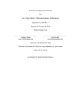
CALIFORNIA STATE UNIVERSITY, NORTHRIDGE
Electronic Power Supply and Sensor Emulator for the CSUNSat1
A Project submitted in partial fulfillment of the requirements
For the degree of Master of Science
in Electrical Engineering
By
James Edward Downs II
December 2013
The thesis of James Downs II is approved:
_________________________________________ _____________
Dr. Ichiro Hashimoto
Date
_________________________________________ ______________
Professor James Flynn
Date
_________________________________________ ______________
Dr. Sharlene Katz, Chair
Date
California State University, Northridge
ii
List of Contents
CALIFORNIA STATE UNIVERSITY, NORTHRIDGE ................................................................ i
The thesis of James Downs II is approved: ...................................................................................... ii
List of Contents ............................................................................................................................... iii
List of Figures ................................................................................................................................... v
List of Tables ................................................................................................................................. vii
List of Equations ........................................................................................................................... viii
1 Introduction .................................................................................................................................. 1
2 Background ................................................................................................................................... 2
3 Overview ....................................................................................................................................... 3
4 Electronics .................................................................................................................................... 6
4.1 NXP 2378 Microcontroller .................................................................................................... 6
4.1.1 Serial Peripheral Interface (SPI) ..................................................................................... 8
4.1.1.1 Pin Description......................................................................................................... 9
4.1.1.2 Configuration Registers ......................................................................................... 10
4.1.2 UART............................................................................................................................ 11
4.1.2.1 UART 1 Configuration Registers .......................................................................... 11
4.1.2.2 Baud Rate Calculation ........................................................................................... 13
4.1.2.3 UART Pin Description ........................................................................................... 13
4.1.3 Timer ............................................................................................................................. 13
4.2 MAX 563 UART Controller ................................................................................................ 15
4.3 2 to 4 Decoder ...................................................................................................................... 15
4.4 Digital to Analog Converter................................................................................................. 15
5 MATLAB GUI ........................................................................................................................... 19
5.1 EPSSE .................................................................................................................................. 20
5.1.1 Channel Select .............................................................................................................. 21
5.1.1.1 Function ................................................................................................................. 21
5.1.1.2 Implementation ...................................................................................................... 21
5.1.2 New Section .................................................................................................................. 22
5.1.2.1Function .................................................................................................................. 22
5.1.2.2 Implementation ...................................................................................................... 22
iii
5.1.3 Run Simulation ............................................................................................................. 24
5.1.3.1Function .................................................................................................................. 24
5.1.3.2 Implementation ...................................................................................................... 25
5.1.4 View All ........................................................................................................................ 27
5.1.4.1 Function ................................................................................................................. 27
5.1.4.2 Implementation ...................................................................................................... 28
5.1.5 Save Configuration ....................................................................................................... 29
5.1.5.1Function .................................................................................................................. 30
5.1.5.2 Implementation ...................................................................................................... 30
5.1.6 Load Configuration ....................................................................................................... 31
5.1.6.1 Function ................................................................................................................. 32
5.1.6.2 Implementation ...................................................................................................... 32
5.1.7 Update Plot.................................................................................................................... 33
5.1.7.1 Function ................................................................................................................. 34
5.1.7.2 Implentation ........................................................................................................... 35
5.2 Sine Wave GUI .................................................................................................................... 36
5.3 Slew GUI ............................................................................................................................. 38
5.4 Random GUI ........................................................................................................................ 39
6 Data Loader Software ................................................................................................................. 41
6.1 Startup Code ........................................................................................................................ 42
6.2 SPI Configuration ................................................................................................................ 44
6.3 UART Configuration ........................................................................................................... 48
6.4 Delay Function ..................................................................................................................... 50
6.5 Main ..................................................................................................................................... 51
7 MATLAB Real time Plot ............................................................................................................ 58
8 Schematic .................................................................................................................................... 61
8.1 Simulator Box ...................................................................................................................... 61
8.2 Electrical Connections ......................................................................................................... 63
9 Conclusion .................................................................................................................................. 65
References ...................................................................................................................................... 66
Appendix........................................................................................................................................ 67
iv
List of Figures
Figure 1: System Block Diagram ..................................................................................................... 5
Figure 2: NXP2378 Block Diagram [1] ........................................................................................... 8
Figure 3: SPI Protocol...................................................................................................................... 9
Figure 4:8 Channel DAC configuration [2] ................................................................................... 16
Figure 5:AD7303 Internal Logic [2] .............................................................................................. 17
Figure 6: EPSSE Main GUI ........................................................................................................... 21
Figure 7: Save Configuration Prompt ............................................................................................ 30
Figure 8: saveTestConfig Callback ................................................................................................ 31
Figure 9: loadTestConfig Callback ................................................................................................ 33
Figure 10: UpdatePlot_Callback .................................................................................................... 35
Figure 11: getDuration Function .................................................................................................... 36
Figure 12: Sine Wave GUI ............................................................................................................ 37
Figure 13: Sine Wave Example ..................................................................................................... 38
Figure 14: Slew Rate Example ...................................................................................................... 39
Figure 15: Random GUI ................................................................................................................ 40
Figure 16: Stack and Heap Configuration section in Startup file .................................................. 43
Figure 17: Configuration Wizard ................................................................................................... 43
Figure 18: Flow of Data ................................................................................................................. 44
Figure 19: SPI Timing ................................................................................................................... 45
Figure 20: SPI_config.c ................................................................................................................. 46
Figure 21: send8Bits Flow Chart ................................................................................................... 48
Figure 22: Send 8 bits function ...................................................................................................... 48
v
Figure 23: UART configuration and functions file ........................................................................ 49
Figure 24: sendData Function Flow Chart ..................................................................................... 50
Figure 25: Delay Function C Program ........................................................................................... 51
Figure 26: Main Loop Flow Chart ................................................................................................. 52
Figure 27: Main Function .............................................................................................................. 53
Figure 28: sendSignalsTime Flow Chart ....................................................................................... 55
Figure 29: sendSignalsTime function ............................................................................................ 55
Figure 30: sendSignalsForever Flow Chart ................................................................................... 56
Figure 31: sendSignalsForever Function ....................................................................................... 57
Figure 32: Signal 1 Design plot in Main GUI ................................................................................ 60
Figure 33: Real Time Plot for Signal 1 .......................................................................................... 60
Figure 35: EPSSE Simulator Box Front Panel............................................................................... 62
Figure 36: Inter Connect Diagram ................................................................................................. 63
Figure 37: SPI Emulator ................................................................................................................ 69
Figure 38: SPI Configuration Emulator Validation ....................................................................... 70
vi
List of Tables
Table 1: SPI Pin Description [1] ................................................................................................................... 10
Table 2: SPI Registers [1] ............................................................................................................................. 10
Table 3: UART 1 Configuration Registers [1] .............................................................................................. 13
Table 4: UART Pins [1] ................................................................................................................................ 13
Table 5: Timer Registers [1] ......................................................................................................................... 14
Table 7: Host PC to Microcontroller ............................................................................................................. 63
Table 8: Microcontroller to Electronics PWA ............................................................................................... 64
vii
List of Equations
Equation 1: Baud rate Calculation [1] ........................................................................................................... 13
Equation 2: AD7303 Transfer Function ........................................................................................................ 15
Equation 3: Slew Rate Equation .................................................................................................................... 38
viii
ABSTRACT
Design of an Electronic Power Supply and Sensor Emulator for the CSUNSat1
By
James Edward Downs II
Master of Science in Electrical Engineering
A Cubesat is a miniature satellite which is launched into Low Earth Orbit, and has become quite popular
amongst hobbyist and institutions. The size of the satellites and the complexity of the system as a whole
make the projects very educational for students or any others who wish to further their knowledge in
engineering. The CSUNSat1 is a Cubesat project taken on by California State University Northridge
(CSUN), in collaboration with Jet Propulsion Laboratories (JPL).
The Electronic Power Supply and Sensor Emulator (EPSSE) serves the purpose of testing the CSUNSat1
system during the development stages. For example testing what would happen if for some reason the
CubeSat processor loses power for an amount of time, or the temperature rises to a certain limit, how would
the software be able to handle this problem and what would be the result.
To test the CSUNSat1 the voltage or current levels of a temperature or power supply must be simulated.
Testing of electronic systems has in the past been accomplished using traditional tools like function
generators. To test the CSUNSat1, a system has to be designed in order to simulate more than one signal,
and should be easily configured by the user.
The EPSSE is a Graphical User’s Interface (GUI) designed in software, and electronics which serve the
purpose of realizing the user’s test profile created in the GUI. The goal is to design a GUI which gives the
ix
user an easy method of configuring a test, while offering the capability to fully test the CSUNSat1
microcontroller’s software. The CSUNSat1 microcontroller software will be responsible for monitoring the
currents and voltages of the power supply, various sensors, and the batteries under test.
The reason for designing a GUI based test system is due to the recent popularity of visually based test
equipment, and the idea of carrying out long exhaustive test on a system that may take much longer to
configure than to actually run the test. The GUI was designed in MATLAB and the electronics involve a
microcontroller, a digital to analog converter, and miscellaneous components. The end product is
essentially a programmable arbitrary waveform generator.
x
1 Introduction
This report is a description of the Electronic Power Supply and Sensor Emulator (EPSSE) test
system designed to test the CSUNSat1 functionality. The report will give a background of test equipment,
which will be followed by an in depth description of the EPSSE. Then followed by a tutorial on how to use
the EPSSE. This report can serve as a user’s manual or design report.
Traditionally test equipment is made per the design. The purpose of any test equipment is to test
the functionality of the design. The main functions of the CSUNSat1 is to a) survive in low earth orbit
(LEO), b) monitor the voltage and current levels of the payload, and c) transfer that information down to
mission control (CSUN campus). The EPSSE will test the CSUNSat1’s capability to measure the voltage
and current levels of the payload.
Before moving on, it should be stated that when referring to a GUI action
Select = left mouse click of push button
1
2 Background
This test system will have the capability to simulate eight different sensors, or eight different
voltages, or a combination of both. Therefore to start, a brief introduction as to what a sensor is or how to
measure a physical characteristic is important. A sensor is a transducer, meaning a physical phenomenon is
measured, such as pressure, temperature, etc, and converted into an electrical signal (voltage, or current).
This electrical signal will change based on a change in the physical phenomenon. After the voltage is
sampled and conditioned, this voltage will indicate a measurement. It is the duty of the electronic system
to be able to condition, sample and compute the measurement.
To validate any electronic design, ensure it meets requirements a test system is built. This is most
likely part of the design process. The idea behind test equipment is to simulate a voltage or current in order
to validate the electronic system is working. To validate this many elaborate test systems and stations have
been developed and implemented. The broadness of test system and cost of the test system is usually
dependent on the requirements for the testing the system. These requirements are usually stipulated by the
customer. The design of the test equipment is usually designed in parallel.
The need for test equipment has become so customary that a specific type of engineer (Test
engineer) is one of the most sought out engineers in the field today. This specialized Engineer is
responsible for testing and validating electronic components and designs [6].
Test equipment software and companies are now some of the biggest employers of young
engineers, and LABVIEW (a common test equipment software and hardware company) equipment of some
sort is in almost every engineering company’s lab or office.
2
3 Overview
The requirements for the EPSSE are derived from the Requirements for CSUNSat1 Revision 1.1.
The JPL experiment section 3.2.10 requires that the CSUNSat1 main processor shall use temperature,
current, or voltage data from the experiment to control the timings, connections, charging magnitudes and
discharging magnitudes of the experiment. Section 3.2.11 states the main processor shall protect the space
craft from experiment faults. The main processor shall sample the voltages as a rate of 1Hz, which may
vary between 0 – 5V +/-0.1V. There will be six voltages.
The EPSSE is a device which is composed of electronics, for creating voltage and current
simulation, a GUI which allows the user to configure the desired simulation, and the software which serves
the purpose of loading the electronics with the files configured in the GUI. The EPSSE simulator box will
provide eight channels or signals and thus the GUI will involve configuring these 8 channels.
The EPSSE GUI was designed to test the CSUNSat1’s ability to meet the requirements in the
Requirements for CSUNSat1 Revision 1.1 document. The four design goals are as follows:
1. The EPSSE GUI is designed as to offer the user the most user friendly means of configuring a
test or simulation.
2. The values calculated and stored are meant to output values thru the electronics which would
range from 0 to 5.25 volts.
3. The values would be output at a rate of 10Hz or 1 sample every millisecond. This is faster than
the required sample rate [7]. The max slew rate now set at 5.25V/mSec.
4. The test or simulation would be able to last long enough to test the ability of the processor to
endure power loss during eclipse or loss of sunlight for some reason.
When the EPSSE is being utilized to test the CSUNSat1, the system configuration is that of figure
1. The system consists of two major hardware components. 1) A Personal Computer, and 2) The EPSSE
Simulator Box. Inside the EPSSE box is all of the electronics hardware, and interconnections. The Host
3
PC is where the user will configure the test simulation, while the EPSSE Simulator Box contains the
electronics needed to implement the simulation.
4
Host PC
Contains GUI
Environment
`
EPSSE Simulator Box
AD7303
2 Channel
DAC IC
MCB2300
Development
Board
74HC139
2 to 4
Decoder
AD7303
2 Channel
DAC IC
AD7303
2 Channel
DAC IC
NXP2378
microcontroller
and COM Ports
Electronics
CSUNSat
uController
Figure 1: System Block Diagram
5
AD7303
2 Channel
DAC IC
4 Electronics
The Electronics is composed of a microcontroller (NXP2378), contained on the MCB2300
development board. A digital to analog converter (DAC), a decoder, 4 AD7303 Analog Devices serial
communication DAC’s. The microcontroller is an NXP2378, which utilizes the ARM7 architecture. The
MCB 2300 Development board contains various electronics [8] for programming the NXP2378, and for
communicating with other devices. Two COM ports, have a UART communications protocol. One of
these ports can be used with a serial to USB cable to program the NXP2378. The MCB2300 board
contains an IC MAX563 UART to serial converter IC [9].
4.1 NXP 2378 Microcontroller
The NXP2378 is an ARM7TDMI-S microcontroller. The NXP2378 contains several peripherals
(figure 2), but this paper will only cover in detail the peripherals and functions which are used. Refer to the
UM10211 NXP23xx User’s Manual for all peripherals and configuration. All peripherals are configured by
setting bits in memory mapped registers. Each memory location contains one byte.
The NXP2378 has memory allocation for flash programming of 512KB. This accounts for 512KB
of memory for the program, and the data which makes up the signals sent to the electronics. This was
considered when deciding on the rate the values are sent to the CSUNSat1 main processor. Each value can
be set at 8 bits, but this will allow 512KB-Program memory for the values. The hex file is 6KB this leaves
506KB for the values. That is 506,000 locations.
506,000 = 60 (𝑠𝑒𝑐𝑜𝑛𝑑𝑠) ∗ 60 (𝑚𝑖𝑛𝑢𝑡𝑒𝑠)ℎ𝑜𝑢𝑟𝑠 ∗ 8 (𝑐ℎ𝑎𝑛𝑛𝑒𝑙𝑠) ∗ 10 (𝑠𝑎𝑚𝑝𝑙𝑒𝑠 𝑝𝑒𝑟 𝑠𝑒𝑐𝑜𝑛𝑑)
Equation 1: Equation for Allocation of memory
6
Table 1: Max Hours of Simulation per Channel
Channels
Max (hours)
8
1.75
7
2
6
2.34
5
2.811
4
3.51
3
4.68
2
7.02
1
14.05
The max hours for each channel are shown in table 1.
7
Figure 2: NXP2378 Block Diagram [1]
4.1.1 Serial Peripheral Interface (SPI)
The SPI is a full duplex synchronous serial communication protocol. Which means that data is
sent out in sync with a clock, and data can be sent to and from on the same bus. As can be seen below the
SCK is the master clock and depending on the configuration the data is clocked out on the rising or falling
8
edge of the SCK. The Slave Select (SSEL) line is an active low line, and must be asserted for the data to be
received by the slave. This serves as a sort of handshaking for the two devices [3]. The SSEL line can be
any signal which will can drive an output to be a low (below 0.8V, for CMOS), and does not have to be the
specific SSEL line designated in the memory mapped IO.
Figure 3: SPI Protocol
An SPI interface is configured using a master and a slave. The master has the responsibility of providing
the clock. The SPI registers are memory mapped on the NXP2378, and communicate with the ARM7
microcontroller over the Advanced Peripheral Bus (APB).
4.1.1.1 Pin Description
The SPI interface uses 4 pins for interfacing with the other device. These pins are described in
table 1.
9
Name
SCK
SSEL
MISO
MOSI
Type
Description
Serial Clock. Clock sent out by the master if the NXP is configured as master,
Input/output or input clock from device if NXP is configured as slave
Slave Select. The slave select line is a active low signal which is used to
Input
select a device for communication
Master In, Slave Out. If NXP is configured as master then this is the input
Input/Output from the slave device. If the NXP is a slave this is the oupt
Master Out, Slave In. If NXP is configred as master this is the output,
Input/Output if NXP is a slave this is the input
Table 2: SPI Pin Description [1]
Note here that the SSEL line is an input, and this is because if the device is set as a slave, this line will be
an input. As stated before if this line is an output then it can be used as a SSEL line, but does not have to
be set to that in the PINSELx register.
4.1.1.2 Configuration Registers
The NXP2378 has five configuration registers (table 2).
Name
Description
SSPxCR0
SSP control register0
SSpxCR1
SSP control register 1
SSPxSR
SSP Status register
SSPxDR
SSP Data Register
SSPxCPSR SSP Clock counter register
Access
R/W
R/W
RO
R/W
R/W
Address
0xE0068000
0xE0068004
0xE0068008
0xE006800C
0xE0068010
Table 3: SPI Registers [1]
The SPI control registers configures the operation of the SPI. The SPI can be configured to send
anywhere from 8 bits in a single write up to 16 bits. The clock phase and polarity can be set to determine
the relationship between the data being sent out and the clock. The SPI can send LSB first or MSB first,
and interrupts can be enabled with the control register as well.
The Status Register is used to check the status of the transmission of receive operations. A read
overrun indicates that the SPI read buffer contains data that has not been read by the processor, and new
data has already arrived. A write collision will indicate that a write to the SPI data register was done before
10
the data has been sent. If the device is set as a master and the SSEL line goes low and is set as an SSEL
line, then a mode fault will occur, stating that the device is configured as a master, but another device is
treating it as a slave. SPI transfer complete will indicate that an SPI transfer has been completed. This bit
is used to check when new data should be inserted into the SPI data register.
The SPI Data register is a 16 bit register which contains transmit or receive data. The upper 8 bits
are the MSB’s and the lower 8 bits are the LSB’s. If the SPI is configured to send only 8 bits the lower 8
bits will contain the data sent.
The SPI Clock register controls the frequency of the master clock (SCK), and thus controls the
frequency which data is sent out or received. In the Master mode this must be an even number greater or
equal to 8. This register, along with the PCLK register will control the rate at which data is sent or
received.
The SPI interrupt register can be used to generate an interrupt when a SPI transfer is complete, or
there is a mode fault. Please refer to section 6.2 for the configuration for this project and the code which
implements the configuration.
4.1.2 UART
The NXP2378 contains four UART interfaces. One of the UART interfaces is needed for
download of application code, if JTAG is not used. Refer to section 9.1 for instructions of application code
download.
UART1 will be utilized in this project for sending real time data to the Host PC. The host PC will
contain a program which will plot in real time the data being sent to the CSUNSat1 processor. This will
provide the user the ability to validate and observe the response the CSUNSat1 will have to the simulation.
4.1.2.1 UART 1 Configuration Registers
The NXP2378 contains fourteen registers for each of the four UART interfaces. The UART1
registers which are used for this project are described in table 3.
11
Name
Description
Access
Register
RBR
Receiver Buffer Register. Contains 8 bits of data
RO
0xE0010000
THR
Transmit Holding Register. Contains 8 bits of write
WO
0xE0010000
R/W
0xE0010000
data
DLL
Divisor Latch. 8 Least significant bits of divisor latch.
Used to divide the PCLK for setting the desired Baud
(DLAB = 1)
Rate. See Section 4.1.2.3 Setting Baud Rate
DLM
IER
Divisor Latch. 8 most significant bits of divisor
0xE0010004
latch
(DLAB = 1)
Interrupt Enable Register. Enables the Auto-Baud
R/W
time-out interrupt
0xE0010004
(DLAB = 0)
IIR
Interrupt ID Register
RO
0xE0010008
FCR
FIFO Control Register. Reset the RX or RX FIFO , and
WO
0xE0010008
R/W
0xE00100C
RO
0xE0010014
enable FIFO
LCR
Line Control Register. Used to configure the word
length, select 1 or 2 stop bits, enable parity, select parity
type, break control, and divisor latch bit access
LSR
Line Status Register. Indicates a Receiver data ready,
overrun error, parity error, framing error, break interrupt,
transmit holding register empty, transmit empty, and RX
FIFO error
SCR
Scratch Pad Register. Readable and writable register
R/W
0xE001001C
ACR
Auto baud Control Register. Used to control Auto Baud
R/W
0xE0010020
functions.
FDR
Fractional Divider Register. Used to setup the baud rate
R/W
0xE0010028
TER
Transmit Enable Register. Enables a transmit of the
R/W
0xE0010030
FIFO data
12
Table 4: UART 1 Configuration Registers [1]
Notice that some registers are used for multiple purposes. This should be a caveat for the programmer
when configuring the UART.
4.1.2.2 Baud Rate Calculation
The baud rate is configured using equation 2.
𝑈𝐴𝑅𝑇𝑏𝑎𝑢𝑑𝑟𝑎𝑡𝑒 = 𝑃𝐶𝐿𝐾/(16 ∗ (256 ∗ 𝐷𝐿𝑀 + 𝐷𝐿𝐿) ∗ (1 +
𝐴𝑑𝑑𝑉𝑎𝑙
))
𝑀𝑢𝑙𝑉𝑎𝑙
Equation 2: Baud rate Calculation [1]
PCLK – clock supplied to the UART.
DLM – Divide bits (upper)
DLL – Divide bits (lower)
AddVAL – the numerator for a fractional divide value
Mul Val – the denominator for a fractional divide value
4.1.2.3 UART Pin Description
Name
RXD1
TXD1
Type
Input
Output
Description
Serial Receive Data
Serial Transmit Data
Table 5: UART Pins [1]
4.1.3 Timer
The NXP2378 contains four timers which can be used for different purposes. For this project the
Timer0 is utilized to implement a delay. The timer can be configured using the memory mapped registers
outlined in Table 5. The Timer is a 32 bit counter and each of the four match registers per timer can be
configured to cause an interrupt. The timer also contains external match registers which can be enabled to
13
set low, set high, or toggle upon a match condition. Please refer to section 6.4 for the application code
which implements a delay for this project.
Name
IR
Descriptoin
Interrupt Register. Using the VIC a write to the
will clear the interrupt flag. This register can also be
read if polling is being used.
Access
R/W
TCR
Timer Counter Register. The TCR is used to control
the timer functions
Timer Counter. 32 bit register which increments
every PR+1 cycle of the PCLK.
Prescale Register. When the PC is equal to this
value the TC is incremented and the PC is reset
The Prescale Counter is a 32 bit value which
increments on the PCLK
Match Control Register. Used to control if an
interrupt is generated when the TC matches a MR
Match Register 0. Stores value which the TC will
match, and genrate and interrupt, reseet TC, stop
Timer or do nothing
Match Register 1
Match Register 2
Match Register 3
Capture Control Register. Controls which edges of
the capture inputs are used to load the capture
registers
Capture Register 0. Loaded with the value of TC,
when a capture event occurs
Capture Register 1
External match registers. Controls the external
match pins
Count Control Register. Selection between timer or
counter operation
R/W
TC
PR
PC
MCR
MR0
MR1
MR2
MR3
CCR
CR0
CR1
EMR
CTCR
R/W
R/W
R/W
R/W
R/W
R/W
R/W
R/W
R/W
RO
RO
R/W
R/W
Table 6: Timer Registers [1]
The timer does have pins for external match and capture functions, but due to the fact that the timer is being
used as a delay, the pins are not configured and thus not used.
14
4.2 MAX 563 UART Controller
In order for the NXP2378 to communicate through UART, a UART controller is needed. The
MAX53 contains 2 RS-232 drivers and 2 RS-232 receivers. This makes it ideal for the two UART ports
which will be used (1 for the programmer, and 1 for the UART real time data sent to the host PC). This
UART controller is present on the MCB2370 development board.
4.3 2 to 4 Decoder
A simple 2 to 4 decoder is used as a chip select for the four different DAC IC’s. This will create 8
channels. The decoder is a 74HC139 2 to 4 decoder [4]. This decoder is an active low output. So a 0000
will set the 1st output low and all others high, a 0001 will set the 2 nd output low and all others high. This
decoder is used as the select line (SSEL) for the four DAC’s, which is an active low enable. Therefore to
enable the DAC1 a 0000 is sent to the decoder through GPIO pins on the NXP2378. Along with this and
the two channels on the DAC’s it provides five channels.
4.4 Digital to Analog Converter
For this project a DAC IC is used to send out voltages which can then be interpreted by the
CSUNSat1 main processor. These voltages, as stated in the overview section represent the data the
microcontroller would be receiving during its mission duration. The DAC IC is an Analog Devices,
AD7303 [2]. This is a 2 channel DAC which is a full scale DAC, which is capable of communication
through SPI protocol. The shift register is 16 bits wide, which are used to configure and set the output of
each channel. The transfer function of the DAC is as follows:
𝑉𝑜𝑢𝑡 = 2 ∗ 𝑉𝑟𝑒𝑓 ∗ (
𝑁
256
)
Equation 3: AD7303 Transfer Function
Where N is an eight bit hex value. For example
If Vref is set to Vdd/2, selected as internal reference.
15
𝑉𝑜𝑢𝑡 = 2 ∗ 2.5 ∗ (
128
256
1
) = 5 ∗ = 2.5𝑉
2
With 5V for Vdd the max output is 5V. The AD7303 datasheet sets the max Vdd as 5.5V. Which will
indicate that the max output of the AD7303 is 5.5V. For this project four AD7303’s will be utilized to set
up an eight channel configuration. The reference voltage will be selected as the internal reference and thus
Vdd will be set to provide the CSUNSat1 main processor with the required voltage range stipulated in the
requirements document. The Vdd will be supplied from the NXP2378 and will be 5.25 volts. This will
provide the ability to output the voltage range specified in the initial design goals (2).
Figure 4:8 Channel DAC configuration [2]
As can be seen the SCLK and Data lines will all be the same, the only difference is the coded address
which will cycle through the AD7303’s and the Enable line, the decoder will only be enabled right before
the serial data is being sent to the AD7303 device, as advised in the AD7303 datasheet [2].
The AD7303 architecture uses a shift register for the input control bits and data bits, and an input register.
16
Figure 5:AD7303 Internal Logic [2]
Figure 5 shows that the control bits will set the functionality of the device, while the data bits flow
dependent on the control bits.
The input shift register contents indicate as stated before that the upper 8 bits are control bits, and the lower
8 bits are data bits. Bit 15 selects between internal or external reference. For this project the internal
reference is selected which is Vdd/2. Bit 14 is a don’t care bit. Bit 13 is a load DAC bit, its purpose is to
load the DAC registers for a synchronous update. The PDB bit is a power down DAC B bit, and PDA is a
power down DAC A bit. Neither are powered down during the simulation. The A/B bit is used to select
between DAC A and DAC B and with CR1 and CR0, really control how data is loaded into the DAC
registers and how data is sent out of the device.
17
Figure 6: AD7303 Truth Table [2]
As can be seen in figure 6there are a number of combinations. For this project if DAC A is to be used then
the Control bits are set to 0x3, which will set DAC A DAC register to be updated from the shift register and
then the data will be sent out immediately. For DAC B 0x7, will do the same, and thus is what is
configured in the software.
18
5 MATLAB GUI
The GUI for this project was designed in MATLAB. This is due to a couple of reasons, none
taking precedence over the other.
1. MATLAB is a familiar tool for most of the current Electrical Engineering students. If this
project is to be modified at any time in the future, the tools would be available.
2. MATLAB tools for creating a GUI are intuitive and the built in functions included in the library
allow less of a learning curve.
3. MATLAB’s popularity is the reason for a bevy of information and tutorials.
MATLAB uses what is called “guide” (figure 8), to design the GUI visually. To implement a function
simply drag and drop from the options on the left and then resize and position as desired. Each time a
widget (pushbutton, text box, plot, etc.) is created, a callback function is created in an m-file. This m-file
can be edited to implement the functions and task which you would like the GUI to accomplish. Once the
design is finished then select the play button and the m-file is created. The GUI can be updated as desired
by opening the fig file, or editing the m-file. For a more complete tutorial on MATLAB guide and GUI
design please refer to [5].
19
Figure 7: MATLAB guide Blank figure
5.1 EPSSE
The EPSSE GUI is responsible for creating the values that will be loaded into the NXP2378
microcontroller memory. More specifically the values that will represent the voltages. These are hex
values ranging from 0 (0V) to 0x255 (2Vref or Vdd). As stated the GUI was designed in MATLAB, and
the goal of the software, is to provide the user the ability to set up a test or simulation without exiting the
GUI. The Data Loader Software will serve the purpose of configuring the NXP2378, and sending the data.
The details of the Data Loader Software will be described in section 6.
The EPSSE Main GUI is the first GUI which starts when the program is started. This GUI
provides the main screen for the user to design the simulation. The design procedure is described in the
User’ Manual (section 9.3). Although different user’s will configure different tests differently.
20
Figure 6: EPSSE Main GUI
5.1.1 Channel Select
The Channel Select is a dropdown menu which will select the current channel to display.
5.1.1.1 Function
Once a channel has been selected the display will display the current signal designed for that
channel. If the signal for that particular channel has not been designed the display will be empty.
5.1.1.2 Implementation
The following code creates the Channel Select Function. Once the function is created the object
string is set to display Channel 1, Channel 2….to Channel 8. This is implemented using the set function for
that object.
% --- Executes during object creation, after setting all properties.
function ChannelSelect_CreateFcn(hObject, eventdata, handles)
21
if ispc && isequal(get(hObject,'BackgroundColor'), get(0,'defaultUicontrolBackgroundColor'))
set(hObject,'BackgroundColor','white');
end
set(hObject,'String',{'Channel 1','Channel 2',...
'Channel 3','Channel 4','Channel 5',...
'Channel 6','Channel 7','Channel 8'});
5.1.2 New Section
The New Section button is located to the right of the Channel Select dropdown menu, and is a
push button.
5.1.2.1Function
The function of the New Section button is to call a dialog message; this dialog message will
prompt the user to choose what type (Sine Wave, Random, Slew) of new signal the next section or first
section will be. Once the button is pressed it will also increment the New Section number.
5.1.2.2 Implementation
The NewSection Callback opens a question dialog and prompts the user to select. A function was
designed to set NewSection implementing a switch statement. Depending on the statement selected a
specific GUI will start which will give the user the options to select the parameters. The NewSection data
22
is then set as an object to pass to the GUI which will be opened. This is done with the setappdata
MATLAB function.
% --- Executes on button press in NewSection.
%opens dialog box and updates section number
function NewSection_Callback(hObject, eventdata, handles)
NewSection = handles.NewSection;
chioce = questdlg('What type of Signal?',...
'choice','Sine Wave','Slew', 'Random','Random');
NewSection = setNewSection(chioce,NewSection);
handles.NewSection = NewSection;
set(handles.SectionNumber,'String',NewSection);
guidata(hObject,handles);
%make data avaiable for Section_Plot GUI
hMainGui = getappdata(0, 'hMainGui');
setappdata(hMainGui,'NewSection',NewSection);
%-------------------------------------------------------------%setNewSection set the new section GUI based on the user input
%if a new plot is created then increment NewSection Number
%else keep it the same
%-------------------------------------------------------------function [NewSection] = setNewSection( x , NewSection )
switch x
case 'Sine Wave'
23
run('Sine_Wave');
NewSection = NewSection+1;
case 'Slew'
run('Slew');
NewSection = NewSection+1;
case 'Random'
run('Random');
NewSection = NewSection+1;
otherwise
NewSection = NewSection;
end
In MATLAB the Switch or Case statement syntax is different from C, an Otherwise is used to set the
default condition. As can be seen if the user selects any of the options, then the NewSection variable will
be updated, if not then the default condition is to leave the variable as it was before. This is important
because the variable NewSection is used to pass arguments back and forth between the GUI’s.
5.1.3 Run Simulation
The Run Simulation is a push button which should be used once the final signal for all channels
has been created.
5.1.3.1Function
The function of Run Simulation is to do run three main tasks. The first is to create or update all of
the signal files that are for the Data Loader software. These are .h files, and are includes which contain
information about the signals timing, duration and parameters. Second is to start the build process, and
download of the software into the microcontroller. This will be done by starting a batch file, which is
24
created and stored in the file system. This file should not be modified. Third is to start the real time plot in
MATLAB, which will plot the data in real time as the signals are being sent out to the electronics the
signals are also being brought into the Host PC by way of UART, which is sampled and plotted.
5.1.3.2 Implementation
When the code is run on the electronics, it is important to set how long the simulation will run. The length
should be set to the longest signal created. For example if a sine wave is created on channel 1 that is 10
seconds, and a random signal is created on channel 2 which is 5 seconds, then the simulation should run for
10 seconds, and then repeat or end. This is the purpose of lines 437 to 448. The lengths of each signal will
be put in a vector, and then the max length will be put in a vector and then the max of that vector will be
used to pad the other signals with zeros.
Then the code will first open a file and name that file. Note this should be in the same location as the
included c file in the Data Loader Software. This is done for all channels. The function make_file is used
to make a c file with an array of values. These values are the values that will be sent out on the serial data
line to the DAC IC’s.
25
The function will call a function which is convert_hex, that will pass the variable signal, and return the
signal_hex variable. The purpose of this function is to convert the signal vector to a hex value, which is
what the DAC needs for a proper output. Once the signal is returned the rest of the function creates a file
and the signal array for each channel. The control and code bits for each channel are hard coded.
The convert_hex function converts the value the value based on the transfer function of the AD7303
(Equation 2).
26
The end of the code in this function will get the value of the togglebutton1, this is the continuous button.
The test will run until power is cut or there is some sort of fault. The Total Test Input box will set the
number of times through the set of signals. The default is set to 1.
5.1.4 View All
View All is a push button which allows the user an option to observe all of the signals. This can
be of use when the user has created a signal, but does not remember what the signal for a specific channel
might be. This can also give the user a representation of the signals once the design has been created.
5.1.4.1 Function
As stated in the introduction, this feature simply plots all of the signals on one widget.
27
5.1.4.2 Implementation
To implement this code a simple subplot is created.
%-------------------------------------------------------------% --- Executes on button press in ViewAll.
%shows a plot of all of the Channels which have been created
%-------------------------------------------------------------function ViewAll_Callback(hObject, eventdata, handles)
figure(1)
subplot(4,2,1);
plot(handles.n1,handles.u1);
title('Channel 1');
subplot(4,2,2)
plot(handles.n2,handles.u2);
title('Channel 2');
subplot(4,2,3)
plot(handles.n3,handles.u3);
title('Channel 3');
subplot(4,2,4)
plot(handles.n4,handles.u4);
title('Channel 4');
subplot(4,2,5)
plot(handles.n5,handles.u5);
title('Channel 5');
28
subplot(4,2,6)
plot(handles.n6,handles.u6);
title('Channel 6');
subplot(4,2,7)
plot(handles.n7,handles.u7);
title('Channel 7');
subplot(4,2,8)
plot(handles.n8,handles.u8);
title('Channel 8');
5.1.5 Save Configuration
The save configuration is a button that will save the current test configuration. Once the button is selected
then a pop up will prompt the user to save the file and in the desired location
29
Figure 7: Save Configuration Prompt
The file should be saved as a .dat file.
5.1.5.1Function
The function of this push button is to give the user a way to configure a test without designing all of the
signals again, if for some reason the test has been aborted, or some other issue arises.
5.1.5.2 Implementation
To implement this function the MATLAB functions uiputfile, fwrite, fopen and fclose are used. Uiputfile
is a function that will open the user input prompt for the user to save the file and in a specific location. The
fwrite function writes data to a dat, or bin file (dependent upon the user). Fopen and fclose functions
simpliy open and close documents in the Host PC, fopen is used to open the file with writer permission
only. This is done so that no data is somehow read from the file. The fwrite in this case first will write the
length of the signal to the file as an unsigned integer (uint32), and then write the rest of the data as a 64 bit
floating point number (single).
30
Figure 8: saveTestConfig Callback
5.1.6 Load Configuration
The Load Configuration push button will prompt the user to load a .dat file, which was created before and
saved.
31
5.1.6.1 Function
This is used in conjunction with the Save Configuration push button. The user can load previously saved
files once this button is pressed and use those previous configurations to quickly set up the test, thus
reducing the time to gather more important data.
5.1.6.2 Implementation
The loadTestConfig callback function will open a prompt with the uigetfile MATLAB function. The file
will be opened with read only permission. A for loop is set up to set the length of each file by reading the
first unsigned integer value. The fseek function will go to the location of the first value, and then fread will
read all of the values and store each in an array signified by u(I,:).
32
Figure 9: loadTestConfig Callback
5.1.7 Update Plot
The Update Plot push button is located at the top left of the GUI.
33
5.1.7.1 Function
The Update Plot button will plot a matrix of u(n) on the y axis with n(n) on the x axis, with n
ranging from 1 to the number of channels. The plot will depend on the selection of the Channel. In
programming language this is a switch statement with cases ranging from 1 to number of channels.
For Example, if there are four channels, then there are four different cases, and the syntax in MATLAB is
Switch variable
Case 1
Implementation for variable = 1
Case 2
Implementation for variable = 2
.
.
.
Case 4
Implementation for variable = 4
For this design the variable is Channel, which is the value from the ChannelSelect handle. This can be
obtained from
Channel = get(handles.ChannelSelect,'Value');
This line of code uses the get function to grab a value in the handles structure. Here handles is a structure
of data for the call back. The get function in MATLAB is similar to the get function using C++ in which
the data is private and to access that data a function to get the data must be used. This is a technique called
34
data hiding or data abstraction. This is a feature that makes MATLAB so useful, in that when this is
created the Callback function automatically creates this structure and the get and set functions are built in to
the library.
Once the case has been met, then the implementation will clear the plot, compute the sample rate, and
compute the signal. The sample rate for this project was chosen to be 1KHz. This should be more than
enough to provide proper testing.
After the proper data has been created the data will be plotted, saved and made available to the rest of the
functions in the GUI. The data is made available so that it may be plotted if a View All button is pressed or
if the Channel Select is changed back to a channel that has already been designed.
5.1.7.2 Implentation
Figure 10: UpdatePlot_Callback
35
Figure 7 is just part of this callback, but the rest of the switch is identical except for the return values and
the handles which are created. The Value of ChannelSelect will first be acquired and then based on that
value the correct data will be plotted and saved to the correct handles. For example if the Channel Select
has a value of 1, indicating Channel 1 is selected once the ”Update Plot” button is selected the n1, and u1
will be created and plotted. The variable n1 is referring to the number of samples which will be taken, if
the duration is 2 seconds then the value of n1 should be 10*2 due to a sample rate of 10Hz. The function
getDuration will grab data from all of the other GUI’s (Sine_Wave, Random, and Slew), if the data exist, if
not then this data is set to 0. If the data was not set to 0, then the function would not run and the sequence
of operations would stop. The variable u1, is a vectored array of all the signals that are created. Thus the
reason for incrementing the “New Section” number.
Figure 11: getDuration Function
5.2 Sine Wave GUI
Once the New Section push button is selected a question box will appear, this box will prompt the user to
select which type of wave form the user would like to design. This is a starting point. The idea behind this
is to give the user the ability to customize the test. For example it may be desired to test the nominal case
for a period of time, and then for one minute or so go out of the nominal range. For this reason three
different types of waveforms can be selected as a starting point.
If a sine wave is selected then, the Sine Wave GUI is opened.
36
Figure 12: Sine Wave GUI
Observing figure 12, the Sine Wave GUI will open with a simple plot and parameters to customize the
waveform. The amplitude is half of the peak to peak value. The frequency is in cycles per second, the DC
box provides a DC offset for the signal and the Duration is the duration of the signal in seconds.
To create the sine wave with a peak to peak amplitude of four, a frequency of two and a DC offset of four,
for duration of one second. Simply enter in the values.
37
Figure 13: Sine Wave Example
As can be seen in figure 13 the plot is created and can be added to the EPSSE GUI by selecting the Update
Plot push button on the EPSSE GUI. The sample rate for all signals is hard coded in the software to be
10Hz. Once the signal is plotted the data array is sent to the EPSSE GUI by using the setappdata function
in MATLAB.
5.3 Slew GUI
The same idea as the Sine Wave GUI is implemented in the Slew GUI. As the name suggest this
is a plot of a slew rate, that can be set by the user simply by the
𝒚 = 𝒎𝒙 + 𝒃
Equation 4: Slew Rate Equation
38
M is the slope, or slew rate of the signal in volts per second, and b is the DC offset of the signal. This can
be seen from a formula of
𝑦 = 1𝑥 + 1
Figure 14: Slew Rate Example
As can be seen the signal starts at a 1, with a duration of 1 second and having a slope of 1.
5.4 Random GUI
As with the Sine Wave GUI and the Slew GUI, the Random GUI is used to create a Random
signal.
39
Figure 15: Random GUI
The upper limit is the upper limit on the randomness, for example this Upper limit is 1.1 and the lower limit
is 1, thus the values will range from 1 to 1.1. The duration is 1 second. The random values are generated
using a function which returns values that are Gaussian random distribution.
40
6 Data Loader Software
As stated in the Section 3 Overview, once the design is configured in the GUI, the software has to
be downloaded to the microcontroller in order to run the test. The software that sets up all of the
peripherals, and imports the files and values has the project name Data_Loader. The software’s main
function is to import the values which configure the test, hence the name Data_Loader. The software is
written in the C programming language, with a function based approach.
The software is written so that a continuous flow of data is sent out to the Electronics, and sent
back to the Host PC for real time data plotting. The flow diagram below indicates the flow of data during a
simulation. As can be seen once the data is stored on the microcontroller in program memory (nonvolatile), then the data is sent out to the electronics then sent back to the Host PC, this will repeat for the
number of channels. The that loop will repeat for the duration set in the EPSSE GUI, or run forever if that
is set in the EPSSE GUI. This is controlled using ifdef directives in the software.
Special consideration was taken so that the data would be sent out abiding by the timing which is
set in the MATLAB GUI. Another word, the actual signals (voltage levels and timing) should match what
was designed in the GUI.
41
Data is configured in
Matlab
Data Stored Locally
on Host PC in
respective Files
(Signal_N) for N = 1
to #of Channels
Data Sent to the
NXP2378 over
UART0 COM0
Data Sent out on SPI
Bus to Electronics
Board
This step is
repeated for the
Duration of the
test set in EPSSE
GUI
This step is
repeated for the
# of Channels
Data Sent back to
Host PC over UART1
COM1
6.1 Startup Code
Each time the microcontroller is reset the bootloader configures the NXP2378 for the In System
Programming (ISP), or In Application Programming (IAP). For this project ISP is used and flash memory
is programmed over the UART0 port. This port is brought out on the board through the COM0 port.
Once the bootloader program is finished the startup code is ran. The startup code is a file that is
included with the Keil IDE software. The startup code file is LPC.2300.s. This file can be used to setup
the initial configuration of the NXP2378. The file is setup as to provide a configuration wizard, which
42
allows the user to easily configure the NXP2378. The configuration wizard is a GUI like interface. This
file can be in C/C++ or assembly. Here is an example to illustrate:
Figure 16: Stack and Heap Configuration section in Startup file
Figure 17: Configuration Wizard
43
Looking at figure 16 and figure 17, the highlighted box code corresponds to the configuration wizard in
figure 17. Any change in the configuration will change the assembly code. This is very useful for initially
configuring such peripherals on startup like Clock Setup for the PLL.
If the reset button on the EPSSE Simulator box is pressed the microcontroller will reset and the
simulation will start over from the beginning. Observe the start LED to indicate the beginning of the
simulation. The delay for start of simulation is hardcoded at a delay of 5 seconds. The startup code for the
EPSSE Data Loader will be used to set the timing for the PCLK, CCLK, and power enable for peripherals.
The PCLK and CCLK are used to clock the peripherals on the NXP2378.
6.2 SPI Configuration
The Serial Peripheral Interface (SPI) is a communication protocol which will be used in this project to
interface with the Digital to Analog Converter (DAC). The SPI will send data that was computed in the
EPSSE GUI.
Compute Data in
HEX
Save file which
contains an array of
HEX data
Send the Data over
SPI to the DAC
Figure 18: Flow of Data
44
As can be seen in figure 18, the SPI is responsible for transferring data to a device that can send out a
voltage. According to the AD7303 DAC data sheet, data is clocked in to a shift register which is 16 bits
wide. The first 8 bits are control bits, while the last 8 bits are the data. The SPI is configured first by
setting the SPI0 control register and setting the Clock counter register. Of course the proper configuration
of the pins using PINSELx registers should be set to configure the multiplexed pins on the NXP2378. The
SPI is configured for 8 bits with no interrupts and set as the master. The device will always act as the
master for this project, due to the fact that the AD7303 does not have the capability to write data back to
the NXP2378. The clock counter is set to 6MHz. The PCLK for the SPI is the set at 12MHz. This is a
clock rate of PCLK/8, which is under the required max clock rate of the AD7303, which is 30MHz. It also
fits the stipulation of a value of greater than 8 for a master.
Figure 19: SPI Timing
Firgure 19, shows that for a write to the 4 DACs twice, each time a write occurs there is 16 bits of
data written to each. First the control bits, and then the Data bits. As can be seen the time is 10Hz, or 0.1
seconds. The MATLAB GUI calls for 10 samples per second. This meets the design goal (3).
The SPI protocol is set up in the SSP0 peripheral on the NXP 2378. This peripheral can be set up
as a SPI, 4 wire SSI, or microwire. For this config file getters and setters are used, and the SSP0 or SSP1
defines are used to set this up.
Figure 18 shows the c file which contains the functions for setting and getting the SSP peripheral.
45
Figure 20: SPI_config.c
The send8bits function is used to send 8 bits of data, two times consecutively. First the MSB to
bit 8 is sent as the control bits. The SSP status register is polled to observe when the send data register is
empty. Polling was decided above using interrupts, because in this situation an interrupt would take longer
to service, then to just poll the bit in the status register. As can be seen in the code (figure 22), there is no
process of clearing the status bit, this bit is self clearing.
46
Start from
sendSignalsForever
or sendSignalsTime
Set P0.4 Low
(Enable Decoder)
IOPIN0 =
codeBits&0x3
(Set code bits with
mask)
Is the data
gone from
transmit
register?
No
Check again
Until
register is
empty
No
Check again
Until
register is
empty
getSSPStatus &
0x1 = 0?
Yes
Send the
control bits
for the DAC
Refer to
section 4.4
figure 6
Is the data
gone from
transmit
register?
sendSSPData
(control)
getSSPStatus &
0x1 = 0?
Yes
Send the
data bits to
the DAC
sendSSPData
(signall)
Send the
data to the
UART
sendData(signal)
Exit back to
sendSignalsTime or
sendSignalsForever
47
Figure 21: send8Bits Flow Chart
Figure 22: Send 8 bits function
6.3 UART Configuration
To plot real time data, the UART1 is used to interface with the host PC. The data sent out will be
serial and sent out through the COM1 port. The UART is configured to set 8 bits of data at a baud rate of
11584. The signal that is sent out of the SPI is the same that is sent to the UART Transmit holding register.
This will be the data captured by the host PC.
48
Figure 23: UART configuration and functions file
The file simply sets the proper pins on the microcontroller, then sets the baud rate according to the
baud rate calculation given in section 4.4.2.2, and has a function that will poll the Line Status Register bits
for transmission and then set the value that is passed in the function. The Transmit bit is set low before
entering the data in the Transmit holding register, and this will how the data from being transferred to the
Transmit shift register.
49
Start from send8Bits
Is the transmit
FIFO empty?
If THRE bit is set
in LSR then
empty.
Send the data
to the transmit
FIFO
getUARTStatus &
THRE mask != 0?
U1THR = signal
Exit back to
send8Bits
Figure 24: sendData Function Flow Chart
6.4 Delay Function
The delay function is used to set the output rate of the signal. To set up a delay, the Timer on the
NXP2378 is used. This delay function takes an integer variable and creates a delay, which is the value of
that integer. The delay function simply configures the Timer 0 registers and runs a while loop until the
Timer 0 interrupt flag is not set, then clears the flag and resets the Timer.
50
Figure 25: Delay Function C Program
6.5 Main
The main function is used to configure all of the peripherals, and use the functions to send data to
the DAC. The SPI, and UART are configured and then a function to send the data out is ran. This function
will send the data to the DAC for the duration of the simulation. The simulation can be ran for the duration
of the signal designed in the EPSSE GUI, or can run continuously until the reset button is pressed, or the
power is disconnected. Line 59 through 63 implement an ifdef else endif, which will run one or the other
dependent on the selection during the design. There is a delay for the LED to signal the beginning of the
Test. This LED will be present and labeled on the outside of the EPSSE Simulator box.
51
Start
Initialize the clock
memory and
Periphials
Delay for 5 seconds
Turn on Run LED
Configure the SPI
Configure the UART
Run continuous
Test?
Yes
sendSignalForever()
No
sendSignalsTime
Figure 26: Main Loop Flow Chart
52
Figure 27: Main Function
The main function calls functions which are included in the file. Once of those is the sendSignalsForever,
and the other is sendSignalsTime. The sendSignalsTime function is ran in the program if the user has not
checked the Continuous Radio Button in the EPSSE MATLAB GUI. The duration is the variable that is
passed to the function, and is set as a default of 1. Length is set in the EPSSE MATLAB GUI as the max
of all of the signal vectors, thus the inner loop of the program will cycle until the last value of the longest
signal configured in the EPSSE MATLAB GUI.
53
Start
Endtime = 0
Endtime =time?
Yes
Turn off Run LED
No
End
I=0
Enditme = endtime
+1
Yes
I= Length?
No
Send8bits
X8
Delay
I = i+1
54
Figure 28: sendSignalsTime Flow Chart
Figure 29: sendSignalsTime function
55
The sendSignalsForever function will run an endless loop.
Start
I=0
Yes
I= Length?
No
Send8bits
X8
Delay
I = i+1
Figure 30: sendSignalsForever Flow Chart
56
Figure 31: sendSignalsForever Function
57
7 MATLAB Real time Plot
The MATLAB real time plot is a real time plot of the simulation data which is sent to the
CSUNSat1 main processor. This is done over a serial to USB connection from the EPSSE simulator box,
to the Host PC. The NXP2378 utilizes the UART1 communications terminal to send data to the Host PC.
The script is a based on the real time data plot from a serial port, by Moidu Thavot.
The script first sets up eight plots which will fill the screen. These plots are then updated every
100 milliseconds. Which is the rate of output of the DAC IC’s. These values are then converted back and
plotted.
First all instruments are found and deleted, as to not have any conflicts. Then the serial port is
opened all of the properties are set. The COM port should be set according to the proper location. The
screen size is used to set the location of all of the plots, as to make the code portable. Each figure is
configured to be aesthetically pleasing to the user. All labels and titles are also set. This is somewhat of an
initialization.
58
The while loop will update the values for all the plots and then plot each in the appropriate figure. The
loop variable is set from passing the duration computed in the EPSSE MATLAB GUI. This variable will
be the duration of the longest signal.
59
Figure 32: Signal 1 Design plot in Main GUI
Figure 33: Real Time Plot for Signal 1
60
8 Schematic
8.1 Simulator Box
The simulator EPSSE simulator Box is a metal box that houses the electronics and the MCB2300
development board. It was decided that the MCB2300 development board, (as opposed to designing a
printed wiring board which contains the NXP2378, designed specifically for the purpose of this
project),would be a cheaper solution. The MCB2300, provides more functionality than is needed, but as
stated before the design is cheaper and still serves the purpose.
DAC 7303 x 4
Decoder
text
MCB 2300 Development Board
Figure 34: Inside of Simulator Box
Figure 30 shows the orientation and location of the development board and Electronics inside the EPSSE
Simulator Box. None of the electrical connections are shown, and will be shown in the next section. Both
are mounted to the bottom of the box, and the Electronics are mounted above the MCB2300 Development
board by approximately and inch and a half.
61
Power
LED
Reset
Start
LED
Front of EPSSE Simulator Box
Real Time
Data
Signals and Ground
Flash
Programming
Figure 35: EPSSE Simulator Box Front Panel
The power connection is an open port and will not be sealed. This is decided so that it can also serve as
some ventilation for the components inside the box. The temperature of the components is not anticipated
to reach high temperatures, so this is just a precaution. The reset button will reset the NXP2378 and thus
restart the test. The start LED will indicate that the test has started, the power LED indicates that power is
supplied to the box. The COM ports on the front of the box provide the flash programming and real time
data.
62
8.2 Electrical Connections
Figure 36: Inter Connect Diagram
The electrical connections inside the box are indicated in figure 36, and tables 6 and 7. The MCB2300
development board will provide power and ground for the Electronics. The Host PC will communicate to
the EPSSE Simulator box over the two COM ports. A DB15 Connector provides the signals out of the box.
microcontroller
PIN
PORT
N/A
COM0
FUNCTION
Host PC
PORT
LOAD Signal
USB
Data
N/A
COM1
Real Time Data
USB
Table 7: Host PC to Microcontroller
63
DB15 Connector
Ch B
DAC3
Ch. A
Ch. B
DAC2
Ch. A
Ch. B
A
P0.2
141
Ch. A
COM1
COM1
B
P0.3
142
HOST PC
DAC1
P0.15
89
P0.16
90
COM0
COM0
USB
DATA_LOADER PWA
ENABLE
USB
text
SCK
UART1
Real Time Data
LPC2377
Microcontroller
DATAIN
P0.18
86
GND
GND
UART0
Programmer
Ch. A
DAC4
PWR
5.0V
PWR
5.0V
Ch. B
EPSSE Simulator Box
microcontroller
PWA
PIN
PORT
PIN
FUNCTION
66
P0.0
A
DECODER BIT0
67
P0.1
B
DECODER BIT1
54
P1.23
DATAIN
SPI DATA IN
49
P1.20
SCK
CLOCK
116
P0.4
ENABLE
DECODER
ENABLE
PWR
PWR
PWR
POWER
GND
GND
GND
GND
Table 8: Microcontroller to Electronics PWA
64
9 Conclusion
To conclude the design was for a system to test that CSUNSat1 main processor can meet the
requirements step forth in the Requirements document [7]. The goals are to give the user a user friendly
GUI to configure the test, send the data at the correct voltage levels at a rate which the main processor
should be able to sample the data.
This was accomplished using MATLAB to design a user friendly GUI. Writing software which
would send values to the electronics at a rate as to meet the sample rate the CSUNSat1 main processor will
sample data. Implementing an electronics design to output the correct voltage to test the limits of the
CSUNSat1 main processor. Designing the system memory to store enough values to run a test duration
which would test the limits of the CSUNSat1 main processor.
The results show that the EPSSE can output voltages between 0V to 5.25V. The rate the values
change is 10Hz. The total duration per channel used is stated in table 1. The GUI was designed for the user
to save and load configurations, therefore cutting down on setup time. Designed to give the user the option
to create a combination of signals to perform many different test. The EPSSE GUI gives the user the ability
to monitor the data in real time to track any time at which an anomaly occurs, and the user can view all of
the simulation plots at once. In conclusion the EPSSE GUI was designed with the user in mind.
65
References
1. UM10211 NXP2378 USER’s MANUAL, REV. 4.1, September 5, 2012. Copyright NXP B.V 2012
2. AD7303 Data Analog Devices, Sheet One Technology Way, P.O. Box 9106, Norwood, MA 020629106, U.S.A. Fax: 617/326-8703 © Analog Devices, Inc., 199
3. Processor I/O and Handshaking Rev. 2/25/2013,
http://www.ece.uidaho.edu/ee/classes/ECE340/Lecture_Notes/L20/LCDhandshaking.pdf
4. MM74HC139 Data Sheet, Fairchild Semiconductors, Rev. February 1999,
5. MATLAB Creating Graphical User Interfaces, The MathWorks, Inc.3 Apple Hill Drive Natick, MA
01760-2098, © COPYRIGHT 2000–2013 by The MathWorks, Inc.
6. http://en.wikipedia.org/wiki/Test_engineer
7. Reference to requirements specification for CSUNSat1 Revision 1.1
8. MCB2300-v47 Schematic. 02/20/2008, provide by Keil Tools by ARM, ARM INC 4965 Preston Park
Road, Suite 650 Plano, TX 75093
9. MAX563 Data Sheet, MAXIM Integrated Products, 120 Sab Gabriel Drive, Sunnyvale, CA 94086
66
Appendix
10.1 Downloading to Flash Memory
The process to download to flash memory without using the batch file and the EPSSE GUI is
outlines below.
1. From the Keil IDE select the start flash magic icon.
2. The flash magic program will start
67
To configure correctly make sure that the correct COM port is selected and that Baud Rate is correct. The
oscillator should be set to 12MHz, which is what the boot loader selects for the default timing device.
3. Select the correct Hex file. The Hex file should be created once a build of the program is finished.
4. Select the “Start Button” and the code should start downloading to the microcontroller.
10.2 Keil IDE Emulator
The Keil IDE is used for this project for software development and debugging. The Keil IDE
incorporates an emulator in the IDE. This is very useful in debugging code, as will be demonstrated in the
following example. In this example the emulator is used to validate the SPI configuration by stepping
through the main code.
68
To start the build must be clean of errors, and the debug mode must be selected. Then from the tool bar
select “peripherals”. A drop down menu gives you the option to select any of the peripherals, for this
demonstration the SPI was selected. Now as in figure 16.
Figure 37: SPI Emulator
Once the emulator is up as you step through the code the SPI emulator will indicate the configuration of the
SPI.
69
Figure 38: SPI Configuration Emulator Validation
As can be seen in figure 17, the SPI has been configured as the master, with a master clock of 12MHz, and
an 8 bit write mode. For a complete understanding of Keil IDE document xxx.
70
10.3 EPSSE User’s Manual
The EPSSE is designed to emulate the power supply and the sensors for the CSUNSat1 Cubesat.
This user’s manual will serve as a guide for
a. Providing the connection instructions
b.
10.3.1 Hardware Items
The following items are needed and should be used for the connection and use of the EPSSE
1.
EPSSE Simulator Box
TBD
Figure 1: EPSSE Simulator Box
2.
2 Serial to USB cables, 1 for flash programming, and 1 for UART real time data.
3.
Wall power plug, or computer power cord with DC power input plug.
4.
Personal Computer, Workstation or any type of Computer
71
5.
Flash drive with software of software files located on the computer
10.3.2 Hardware Configuration
To set up a test or simulation follow these steps.
1.
First of all the connections between the EPSSE simulator box and the Host computer must be
made. As well as the connection to the CSUNSat1 processor.
2.
First connect the USB to serial cable into the front of the EPSSE simulator box. The connection is
a DB9 connector which is labeled Flash Program and USB to computer
3.
Next connect the USB to serial cable into the front of the EPSSE simulator box, the connection is
a DB9 connector labeled Real Time Data. Serial Side to box, and USB to computer.
4.
Connect the power cord to the EPSSE simulator box.
5.
Connect all cables to USB ports on the computer
6.
If done correctly the Power LED on the box should be lit, and the COM port on the Computer
should recognize the EPSSE simulator box.
10.3.3 COM PORT and Batch File Configuration
The createBatchFile function in the matlab code will create a batch file for the user. Due to the
fact that the compiler and arm tools may be located in a different location on one computer
72
than another, the user must edit the function in order to user this to run the simulation. This is
done by locating the compiler on the computer. This computer stores the compiler at C:\Keil
ARM\ARMCC\bin. This part of the function must be edited! If no then the batch file will not
compile the c program and the test will not run. The drive will be found for the user, but again
the batch file must be located.
Another method would be to build the data_loader project file and create a batch file, edit that
batch file to run the flashcmds.txt, by adding FM @”correct path”. Then in the start function
edit it so that bat is that file and location. It will save much more time to initially set up the
createBatchFile, and therefore a quick hit of the run simulation button will run the test for the
user.
73
10.3.4 Software Configuration
1. Open MATLAB on the Host Computer.
2. Open the EPSSE GUI, by entering run(‘EPSSE’) in the command line in the MATLAB command
window. This can also be done by opening the EPSSE m file and clicking on the run button
*Note if the m- file is not on the computer the GUI will not run. The m-file and all files
associated with the system should be located somewhere on the Host Computer or you have the
flash drive with the file.
74
Information and Help –
Information will give software
designer and Revision Info.
Help gives user option to open
User’s Manual
Update Plot Button- updates
the design of the channel once
the section has been created in
the sub GUI.
73
Channel Select dropdown box
– will display the current
design of that that channel
Continuous, and Total test
section- If continuous is
selected the test will
continuously run, if not the
test will run for a number
of durations set in the box
COM port – shows the com
port connections between
EPSSE Box and Host PC
New Section Button- starts a
new section in the design
View All Button- will produce a
subplot of all of the channels
Run Simulation Button-runs
the simulation once all the
channels are configured
Save and Load Configuration
buttons- saves the current
configuration or loads a
previously save configuration
3. The MATLAB GUI shown above should open. The COM Port box in the upper right hand corner
will indicate which com ports the flash port and the real time port are connected to.
From the Main GUI the user can view each channel one by one by flipping through the channel select
dropdown box.
To configure a simulation the first thing to decide is which channel to configure. For example if the
user has connected channel 1 to a port on the CubeSat main processor, then channel 1 can be
configured by the following steps.
4. To start the design of the test, select the New Section button. This will open a new question box,
which will prompt the user to select a type signal.
5. Depending on the selection a new GUI will open, all of the GUI’s have similarities, a plot, but differ
in the input parameters.
*Note: All signals are digital and thus produce a digital signal at a rate of one value per millisecond.
All signal parameters are initially set to 0. All signals must be set between 0 and 5.30 to comply with
the Vref supplied to the DAC. If any of the signals are set outside this area an error message will
appear and the signal will not be plotted or created.
74
6. Next choose the parameters for the signal.
a) for the Random Plot the Upper Limit and Lower Limit will set the upper and lower bounds of
randomness, the Duration will as in all of the plots set the duration of this section. The
randomness is a Gaussian random value between the upper and lower limit.
75
b) the sine wave GUI provides inputs for amplitude, frequency, DC level and duration. The
equation is set as Amplitude*sin(2*pi*frequency) + DC level.
76
c) the slew plot equation is mx+b.
77
7.
This signal is a random signal which has values ranging from 1 to 1.1 for a duration of 1 second.
8.
Once the signal is created the user can update the main GUI plot by selecting the update plot
button. As can be seen the plot is now updated with the signal. To add another signal stay on the
same channel and select the New Section button again. A new question box will appear again and
the user can select the type of signal desired. Now repeat the step 6, and choose the parameters for
this signal. Each time a new section is selected that section will be concatenated onto the previous.
There is no limit to the amount of new sections. This allows the user the ability to configure many
combinations a specific signal profiles as desired.
78
Notice the New Section edit text box has now incremented. This will indicate how many signal
sections are in work for this channel.
9.
Once all of the sections are finished the next channel can be set up. This is done by selecting the
Channel in the Channel Select drop down box.
79
Notice the New Section box has been reset to 0. If for any reason you need to look at any of the
channel profiles, simply select it from the dropdown menu, and the signal will be displayed on the
Main GUI plot again. Also if at any time the user would like to view all of the signals then select
the View All push button.
80
Each channel will be shown as above. The user can explode a subplot to take up the whole screen
by holding down the number on the keyboard. Once the number key is released the view all plot
will be displayed as it was before.
10. The user can choose to save the test configuration. The configuration should be saved as a .dat
file, which can be stored in the user’s desired location. If the user has previously saved a
configuration then the load configuration button will allow the user to load the .dat file.
11. Once all of the channels have been configured, then the user should decide if the test will run for a
set duration of time, or if the test should run continuously. This is done simply by selecting the
continuous push button.
12. If the continuous push button is not selected, then the test will run for the duration of the longest
signal profile. In the repeat box the user can set the amount of times to repeat.
13. The real time plot radio button will give the user the option to run a real time plot of the signals as
they are being sent out of the EPSSE box.
14. Once all of the test configurations are finished, to start the test select the Run Simulation button,
and the test should begin. A pop up box should appear indicating all of the files have been created
successfully and that the program is now running. The real time plot will appear on the screen if
the user selected the real time plot radio button.
81
82