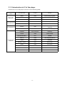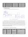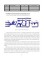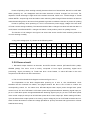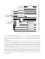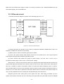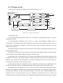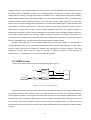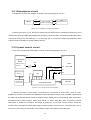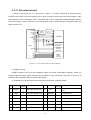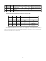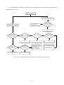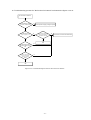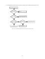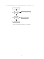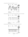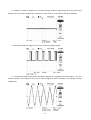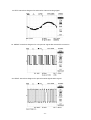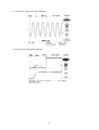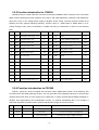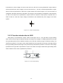
1
DV717 SI &DV721SI
service manual
Catalog
Chapter One About Maintenance
1.1 Safety precautions
1
1
1.1.1 Power supply
1
1.1.2 Precautions for antistatic
1
1.1.3 Precautions for laser head
1
1.1.4 About placement position
2
1.2 Maintenance method
2
1.2.1 Visualized method
2
1.2.2 Electric resistance method
2
1.2.3 Voltage method
2
1.2.4 Current method
2
1.2.5 Cutting method
2
1.2.6 Element substitution method
3
1.2.7 Comparison method
3
1.3 Required device for maintenance
Chapter Two Functions and Operation Instructions
3
4
2.1 Features
4
2.2 Control Button Locations and Explanations
4
2.2.1 Front Panel Illustration
4
2.2.2 Rear Panel IIIustration
5
2.2.3 VFD Display Window Illustration
5
2.2.4 Remote Control Illustration
5
2.3 Accessories
7
2.4 FUNCTION SETUP
7
2.4.1 Function Setup
7
2.4.2 Language
7
2.4.3 Image
7
2.4.4 Sound
8
2.4.5 Playback
9
2.4.6 Karaoke
9
2.4.7 Preference
10
2.4.8 Parental control
10
2.4.9 Initial setup
10
2.4.10 Rest to defaults
10
2.4.11 Exit
11
2.5 Specifications
11
Chapter Three Principle and Servicing
Section One Principle of the Player
12
12
3.1.1 Block diagramof the player
12
3.1.2 PCB board block diagram of the player
12
3.1.2 PCB board block diagram of the player
13
3.1.3 Introduction to IC of the player
14
Section Two Unit Circuit Principle
15
3.2.1 Laser head pin introduction
15
3.2.2 Disc identification circuit
16
3.2.3 Laser power control circuit
17
3.2.4 Reset circuit
18
3.2.5 Clock circuit
19
3.2.6 Disc in/out circuit
19
3.2.7 Main axis braking circuit
20
3.2.8 Mute circuit and power-off quieting circuit
22
3.2.9 Servo circuit
23
3.2.10 Decode circuit
26
3.2.11 Video circuit
27
3.2.12 Audio circuit
28
3.2.13 Power circuit
30
3.2.14 MIC circuit
31
3.2.15 Headphone circuit
32
3.2.16 panel control circuit
32
3.2.17 AV output circuit
33
Section Three Servicing Cases
35
3.3.1 Servicing cases
35
3.3.2 Troubleshooting flow chart
38
Section Four Waveformdiagram
57
Section Five Function Introduction to IC
65
3.5.1 function introduction to Mt1389
65
3.5.2 function introduction to FLASH
75
3.5.3 function introduction to SDRAM
75
3.5.4 function introduction to D5954
77
3.5.5 function introduction to Cs4360
78
3.5.6 Function introduction to CS5340
78
3.5.7 Function introduction to LM1117MP-1.8
79
3.5.8 Function introduction to HS0038A2
79
3.5.9 Function introduction to 4558/TDA1308
80
3.5.10 Function introduction to U501 (FDSH321)
80
3.5.11 Function introduction to ncp1200
81
3.5.12 Function introduction to U503 (LM431A)
81
3.5.13 Function introduction to U502
82
Chapter Four Disassembly and Assembly Process
83
Chapter Cinque PCB board & Circuit diagramt
84
Section One PCB board
84
Section Two circuit diagram
93
Chapter six BOM List
DV721SI Service Manual
100
110
7.1.1 Features
110
7.2.1 PCB board block diagram of the player
111
7.3.1 MIC circuit
112
7.3.2 Control panel circuit
112
7.3.3 Power circuit
113
7.4.1 Troubleshooting flow chart
117
7.5.1 PCB board
120
7.5.2 circuit diagram
127
Chapter One About Maintenance
1.1 Safety precautions
1.1.1 Power supply
When maintenance personnel are repairing DVD players, he should pay special attention to
the
power board with 220V AC and 330V DC which will cause hurt and damage to persons!
1.1.2 Precautions for antistatic
Movement and friction will both bring static electricity which causes serious damages to integrated
IC. Though static charge is little, when a limited quantity of electric charge is added to largescaleintegrated IC, as the capacitance is very small in the meantime, now the integrated IC is very much
easy to be struck through by static electricity or the performance will decrease. Thus static electricity
prevention is of extraordinary importance. The following are several measures to prevent static
electricity:
1. Use a piece of electric conduction metal with the length of about 2 metres to insert into the earth,
and Fetch the lead wire from the top of the surplus metal and connect to the required static electricity
device. The length and depth of the metal embedded under the earth should be determined according to
the wettability of the local soil. For humid places, it may be shorter, and longer and deeper for dry places.
If possible, it can be distributed and layed in terms of “#” shape.
2. On operating table-board, the antistatic table cushion should be covered and grounded.
3. All devices and equipments should be placed on the antistatic table cushion and grounded.
4. Maintenance personnel should wear antistatic wrist ring which should be grounded.
5. Places around the operating position should also be covered with electric conduction cushion or
Painted with antistatic paint.
1.1.3 Precautions for laser head
1. Do not stare at laser head directly, for laser emission will occur when laser head is working, which
will Hurt your eyes!
2. Do not use wiping water or alcohol to clean laser head, and you may use cotton swab.
-1-
1.1.4 About placement position
1. Never place DVD player in positions with high temperature and humidity.
2. Avoid placing near high magnetic fields, such as loudspeaker or magnet.
3. Positions for placement should be stable and secure.
1.2 Maintenance method
1.2.1 Visualized method
Directly view whether abnormalities of collision, lack of element, joint welding, shedding welding,
rosin joint, copper foil turning up, lead wire disconnection and elements burning up among pins of
elements appear. Check power supply of the machine and then use hands to touch the casing of part of
elements and check whether they are hot to judge the trouble spot. You should pay more attention when
using this method to check in high voltage parts.
1.2.2 Electric resistance method
Set the multimeter in resistance position and test whether the numerical value of resistance of each
point in the circuit has difference from the normal value to judge the trouble spot. But in the circuit the
tested numerical value of resistance is not accurate, and the tested numerical value of integrated IC's
pins can only be used for reference, so the elements should be broken down for test.
1.2.3 Voltage method
Voltage method is relatively convenient, quick and accurate. Set the multimeter in voltage position
and test power supply voltage of the player and voltage of a certain point to judge the trouble spot
according to the tested voltage variation.
1.2.4 Current method
Set the multimeter in current position and test current of the player of a certain point to judge the
trouble spot. But when testing in current method, the multimeter should be series connected in the
circuit, which makes this method too trivial and troublesome, so it is less frequently used in reality.
1.2.5 Cutting method
Cutting method should be combined with electric resistance method and voltage method to use.
This method is mainly used in phenomena of short circuit and current leakage of the circuit. When
cutting the input terminal voltage of a certain level, if voltage of the player rises again, it means that the
trouble lies in this level.
-2-
1.2.6 Element substitution method
When some elements cannot be judged good or bad, substitution method may de adopted directly.
1.2.7 Comparison method
A same good PC board is usually used to test the correct voltage and waveform. Compared these
data with those tested through fault PC board, the cause of troubles may be found.
Through the above maintenance method, theoretical knowledge and maintenance experience, all
difficulties and troubles will be readily solved.
1.3 Required device for maintenance
Digital oscillograph ( 100MHE)
TV set
SMD rework station
Multimeter
Soldering iron
Pointed-month pincers
Cutting nippers
Forceps
Electric screw driver
Terminals connecting cord
Headphone
Microphone
-3-
Chapter Two
Functions and Operation Instructions
2.1 Features
This player has employed the new generation DV decode chip with built-in Dolby Digital decoder
which willbring you to a brand-new AV ententainment world. The 2-laser super error-correction
mechanism supports CD-R.
Brand-new AV Effects
1.Compatible with DivX, MPEG4 discs to produce wonderful pictures.
2.108MHz/12bit video DAC, with more vivid and brilliant pictures.
3.Progressive-scan video outputs to eliminate the flickers hardly ouvercome by interlacing scan
and therefore your eyesight will be well-protected. At the same time, the pictures deflnltion Is sharply
enhanced and the pictures will be finer, smoother and stabler
4.Brightness, chroma and contrast adjustment functions to render your eyes more comfortable.
5.Digital echo Karaoke to enable your singing easier.
6.Composite Video, S-Video and Component Video outputs.
7.Bullt-In Dolby Digital decoder, separate 5.1Ch Outputs.
8.Dolby output for 2channel(DOWNMIX).
9.DVD-Audio decoding output to reproduce original and realistic sound effects.
High Quality Digital Audio
1.Optical and coaxial outputs for Digital audio.
2.DTS, Dolby Digital, PCM Digital audio outputs to satisfy the Fans’Ss acoustic requirements.
Many Convenient Features
1.Screen saver protects your TV set carefully.
2.The novel Mp3 playback window GUI provides you a new way to appreciate Mp3 music.
3.Multi-angle playback function makes it possible for you to view a scene from different camera
angles.
4.It’
s possible to select the desired beginning, development and ending of a story.
5.Direct entry into desired scenes(title/chapter/track search).
6.Zooming function to zoom up any playing picture.
7.Capable of playing PAL/NTSC discs.
8.Multiple aspect ratios to fit TV sets of various screen ratios.
9.Parental lock function to prevent children from watching unsuitable discs.
10.Multiple dubbing languages and subtitle languages bring you the best entertainment status all
the time.
Super Compatibility with super VCD, VCD, CD , CD-R , MP3,HDCD,KODAK PICTURE CD etc.
2.2 Control Button Locations and Explanations
2.2.1 Front Panel Illustration
-4-
3
2
4
5
6
8
7
1
POWER switch
5
PAUSE button
2
Disc tray
6
STOP button
3
OPEN/CLOSE button
7
IR SENSOR
4
PLAY button
8
Display windows
2.2.2 Rear Panel IIIustration
8
1
Mixed Audio Out jack
5
Video Component/Y Pb Pr Out jacks
2
5.1CH Audio Out jacks
6
S-Video
3
Digital Audio Coaxial Out jack
7
Video Out jack
4
Digital Audio Optical Out jack
8
SCART Outjack
2.2.3 VFD Display Window Illustration
2
3
4
5
PBC
SVCD
MP3
6
7
ALL
8
9
10
12
11
1
DVD disc
5
DTS
2
PBC
6
VCD、CD、SVCD Disc
10
Repeat
3
Chapter or Track
7
MP3 Disc
11
PAUSE
4
Playback time
8
Playback status indication
12
DOLBY Digital
9
2.2.4 Remote Control Illustration
-5-
PLAY
1
2
3
4
1
15
16
17
18
2
LANG Button
Change the audio language or audio channel
3
6
19
7
20
8
9
10
21
12
13
14
] Button
Open or close the disc tray.
5
11
[
MEMORY Button
Save the playing point or jump to the saved point
22
23
24
25
26
4
DISP Button
Display or hide disc information.
5
NUMBER Buttons
6
BROWSE Buttons
switch new user interface.
27
7
CURSOR Buttons
28
8
SETUP Button
Function Setup.
29
9
[
] Button
Open/close the virtual keyboard function.
10
KARAOKE Button
Karaoke operation menu.
Display DVD menu or open/close PBC.
20
OK Button
21
Cancel Button
22
ZOOM +/-Button
Zoom in/out the displayed frame.
23
[
[
25
[
13
14
28
PEPEAT Button
A-B Button
15
[
] Button
Press once to stand by, Press twice to play.
16
SUBT Button
Change subtitle language, Switch JPEG
display mode.
17
Q-PLAY Button
Set the played image as the power-on logo.
Skip the advertisement/warning and play the
VOL +/- Button
DVD directly.
Increase/decrease volume level.
29
] Button
Repeat the select.
] Button
CAPTURE Button
[
Repeat play.
Skip forward.
27
] Button
Skip backward.
]Button
Stop playback.
26 [
12
] Button
Fast forward play.
[
Fast backward play.
]Button
Play or pause playback.
24
11
18
Change camera angle .
MUTE Button
Press once to mute, twice to turn off.
ANGLE Button
19
-6-
MENU Button
2.3 Accessories
TV system
AUDIO/VIDEO CORD
REMOTE
AAA SITE BUTTERIES
WARRANTY CARD
USER MANUAL
KARAOKE DISC
AUTO
TV scan mode
1PCS
1PCS
2PCS
1PCS
1PCS
1PCS
IS
Video out.
Com.
TV format
LB
Sharpness
L.
Off
Gamma
2.4 FUNCTION SETUP
Brightness
0
Contrast
0
Hue
0
Saturation
0
High
Medium
Low
2.4.1 Function Setup
5.Press [LEFT] button if you want to return to the
previous setup page.
6.Press [SETUP ]to exit the setup menu.
1.Press the [SETUP] button and the screen
displays the selection menu of function setup.
2.4.2 Language
Language
Setup menu
Image
DVD menu
Sound
Soundtrack
Playback
Subtitle
Off
Setup menu
Russian
DVD menu
English
Ukrainian
Soundtrack
Karaoke
Sbutitles
Off
Preference
Parental control
1.Setup menu: This item is used to set the
prompts language on the screen.
◆Optional setting: Russian, English, Ukrainian.
◆Default: English.
2.DVD menu: To set the preference disc menu
lang when playing.
◆Optional setting: Russian, English, Estonian,
Latvian, Kazakh, Romanian, Byelorussian,
Ukrainian, Chinese, Others.
◆Default: English.
3.Sountrack:To set the preference audio
language when playing.
◆Optional setting: Russian, English, Estonian,
Latvian, Kazakh, Romanian, Byelorussian,
Ukrainian, Chinese, Others.
◆Default: English.
4.Subtitles: To set the preference subtitle
language when playing.
◆Optional setting: Off, Russian, English,
Estonian,Latvian, Kazakh, Romanian,
Byelorussian, Ukrainian, Chinese, Others.
◆Default: Off
Initial setup
Reset to defaults
Exit
2.Press the [CURSOR] button to select the menu
to be entered and press the [OK] or button to
confirm. Or press the [CURSOR] button to Exit
item and then press the [OK] button to exit
3.Press [UP/DOWN] arrow to select the desired
item you want to set and press [OK].
For example, press [UP/DOWN] arrows to
select IMAGE and press [OK]. The Image setting
page appears on the screen.
TV system
TV scan mode
AUTO
IS
Video out.
S-Vid.
TV format
LB
Sharpness
Gamma
AUTO
PAL
NTSC
L.
Off
Brightness
0
Contrast
0
Hue
0
Saturation
0
2.4.3 Image.
TV system
TV scan mode
4.Press [UP/DOWN] arrow to select the
SHARPNESS item. Press [OK] to confirm it.
And then press [UP/DOWN] arrow to select the
desired valus.For example: Press[ UP/DOWN]
arrow to select “Medium”,then press [OK], the
TV screen display.
IS
Video out.
Com.
TV format
LB
Sharpness
Gamma
-7-
AUTO
L.
Off
Brightness
0
Contrast
0
Hue
0
Saturation
0
AUTO
PAL
NTSC
1.TV system: This item is used to the video
output system of this unit.
◆Optional setting: Auto, PAL, NTSC.
◆Default: AUTO.
2.TV scan mode: To set Progressive scan,
Interlaced scan mode .
◆Optional settings: Progressive , Interlaced .
◆Default: Interlaced .
3.Video output: To set the types of SCART out
connector.
◆Optional setting: S-Video,Component , SCART,
◆Default: Component
◆When using RGB outputs from the SCART
interface,please select RGB. Other wise ,
please select Com-ponent,and when using SVideo output please select S-Video.
4.TVn format: To set the aspect ratio of this
player’
s output image.
◆Optional setting: 4:3 Pan-scan, 16:9 letterb.,
16:9 TV.
◆Default: 16:9 letterb.
5.Sharpness:Used to set the sharpness of
video outputs.
◆Optional setting: High, Medium, Low.
◆Default: Medium.
6.Gamma emendation:This item is used to setup
the Gamma value of video output.
◆Optional setting: High, Medium, Low, Off.
◆Default: Off.
7.Brightness:Used to set the brightness of video
outputs.
8.Contrast:Used to set the contrast of
video outputs.
9.Hue: Used to set the hue of video outputs.
10. Saturation: Used to set the saturation
of video outputs.
◆Brightness, contrast, hue and saturation
adjusting means:
A. Press [UP/DOWN] arrow in the video setup
menu to select the desired item you want to
adjust. Press [OK] or [RIGHT] button to enter
the item's adju-stment.
B. Press [UP/DOWN] arrow to adjust the setting
value.
1.Mixer...
Configuration
Digital output
Stereo mix
Tuning
Surr. Mix
Low band
5.1
off
Surr. Mix
FSW.
Low band
Channels
Delays
Auto
PRO Logic II
A.Configuration: To set this player’
s DOWNMIX
mode to change multi-channel audio into two
channel audio.
◆Optional setting: Stereo, 5.1
◆Default: Stereo.
B.Stereo mix: To set the output means of the
left or right audio when playing a Dolby disc
with separate two-channel audio.
◆Optional setting: L+R, L, R.
◆Default: L+R.
C.Surr. Mix: To set output means of the surround
left and right audio when playing a stereo disc.
◆Optional setting: Off, sum, Virt.Surr.
◆Default: Off.
D. Low band: select the channel that you desire
to output low frequency signal.
◆Optional setting: Front F, Center C, Surround
Sr, Subwoofer SW.
◆Default: Front F, Subwoofer SW.
E. Channels: To set volume of each individual
channel.
a. Press [UP/DOWN] navigation keys to select
CHANNEL TRIM, then press the [OK] or
[RIGHT] navigation key to select ENTER
SETUP PAGE as shown in the TV screen:
FRONT
Volume L
20
0
surround
R
l
r
0
0
0
Center SW
0
0
b. Press [LEFT/RIGHT] navigation keys to select
the desired channel to adjust.
c. Press [UP/DOWN] navigation keys to raise or
lower volume of the channel.
d. Press [OK] or [LEFT] to return to the Mix..
setup page.
F. Delays: To set delay time of the Center/
Surround/Subwoofer Speaker.
St.
L+R
off
FSW
Channels
Delays
PRO Logic II
Stereo
L+R
Stereo mix
2.4.4 Sound
Mixer...
St.
Configuration
Off
-8-
c. Press [OK] or [LEFT] button to return to Audio
Setting page after adjustments are done.
a. Press [UP/DOWN] navigation keys to select
Delays in Channels item, then press [OK] or
[RIGHT] navigation key select ENTER SETUP
PAGE as shown in the TV screen.
2.4.5 Playback
Advertisemenu
DVD
No
VCD/SVCD
Files
A. P. V
Subwoofer
0cm
Repeat
Off
Center
0cm
Load effect
Off
LS/RS
180cm
1.DVD: set whether information ofadvertisement
and warnings at the beginning of DVD disc is
skipped to play the movie directly.
Always skip ads
◆Optional setting: Yes, NO
◆Default: Number
2.VCD/SVCD: To set the PCB status.
◆When playing Super VCD or VCD2.0 discs, if
thePCB is ON, the menu image displays.
◆Optional setting: On, Off.
◆Default: On.
3.Files:data disc may probably includes Mp3,
JPEG and MPG format files in which you may
select DVD player to read the file type.
◆Optional setting: Audio, Picture, Video.
◆Default: Audio, Picture, Video.
4. Repeat : select the repeat playback mode.
◆Optional setting: Off, Single, all.
◆Default: Off.
5. Load effect: set the may to play JPEG image.
◆Optional setting: Off, from top, from bottom.
◆Default: Off.
b.Press [UP/DOWN] navigation keys to Select
the desired item oup Press [OK] or [RIGHT]
button to enter setting.
C.Press [UP/DOWN] navigation keys to raise or
lower volume.
d.Press [OK] or [LEFT] to return to the Delays in
channels setting page.
G.PRO Logic II: To set PRO Logic II to ON or
OFF. If the TITLE does not support this
function, we recommend that you set this item
to AUTO because it would become worse if the
processing effects were added forcibly.
◆Optional setting: Auto, On, Off .
◆Default: Auto.
2.Digital output: select to set the format and
stream form of digital audio output.
A.SPDIF format:
◆Optional setting: RAW format, SPDIF/PCM.
◆Default: RAW format.
B.LPCM
◆Optional setting: 48 kHz 16 bit, 96 kHz 24 bit,
192kHz24bit.
◆Default: 48 kHz 16 bit.
3.Tuning:
A.Max volume: set the maximum volume limit.
B.Equalizer: To set Equalizer modes.
◆Optional setting: Off, Rock, Pop, Live, Dance,
Techno, Classic, Soft.
◆Default: Off.
C.Echo: To set different sound field effects.
◆Optional setting: Off, Concert, Living room,
Hall,Bathroom, Cave, Arena, Church.
◆Default: Off.
D.Tone balance: to set the tone level to match
your diapason when you're singing
a.Press [UP/ DOWN] cursor buttons to select
"tone"item in Audio Setting page, and then
press [OK] or [RIGHT] button to enter
Adjustment Menu.
◆Method to adjust tone control:
B.Press [UP/DOWN] cursor button to adjust
setting value.
2.4.6 Karaoke
Microphone
Kar. help
Off
On
No ast.
Off
Volume
5
Echo
5
1.Microphone: switch on or off microphone.
◆Optional setting: On, Off
◆Default: Off.
2.Kar. help: select accompany singing means.
◆Optional setting: Channels L, Channels R,
Channels No ast, Channels No voc.
◆Default: Channels No ast.
3. Volume:
A.In microphone setup page, press [UP/DOWN]
cursor to select “Volume”item, and then press
[OK] button to enter the adjustment menu.
B.Press [UP/DOWN] cursor to adjust the setup
value.
-9-
◆Optional setting: On, Off.
◆Default: On.
C.After adjustment finishes, press [OK] button to
return to microphone setup page.
2.4.8 Parental control
On
Microphone
No ast
any
Volume
4
Kid
Echo
4
G
Kar. help
Allowed..
4.Echo:
A.In microphone setup page,press [UP/DOWN]
cursor to select “Echo”item, and then press
[OK] button to enter the adjustment menu.
B.Press [UP/DOWN] cursor to adjust the setup
value.
C.After the adjustment finishes, press [OK]
button to return to microphone setup page.
Microphone
Kar. help
1.Allowed..: To set the parental control ratings to
prevent children from watching the restricted
contents.( In case the discsupports this
function.)
◆Optional setting: any, Kid, G, PG, PG-13, PGR,
R ,NC-17.
◆Default: any.
2.Set password: To set four digit password to
enable you to change the parental control
ratings.
◆Default: 7890
Volume
4
2.4.7 Preference
On
On
Gr. equalizer
Off
Off
Background
std.
Screen saver
On
PGR
NC-17
On
LED Control
PG-13
R
No ast.
Echo
PG
Any
Set password
Old password
New password
Verify
OK
1.LED Control:This item is used set color of led
on the front panel.
◆Optional setting: On, Off.
◆Default: On.
2.Gr. equalizer: This item is used to set wether
the Dynamic Spectrum is allowed.
◆Optional setting: On, Off.
◆Default: Off.
◆Dynamic Spectrum display is invalid in Data
disc、DVD AUDIO playback.
3.Background: This item is used ti setup the sort
of Power-in Logo.
◆Optional setting: Standard, saved.
◆Default: Standard.
NOTE
The Screen Logo refers that use the image
selected by pressing the [CAPTURE] button as
the power-on logo. When in the operation of
changing screen, if the power-on logo has not
set in Screen Logo, the unit will automatically set
the power-on logo as Screen Logo.
4.Screen saver: Open or close the screen saver
function.
Cancel
2.4.9 Initial setup
Auto
PAL
NTSC
Press [UP/DOWN] arrow to select the
desired option and Press [OK] button to confirm
it.
NOTE
In this setup state, you may not press [LEFT]
button to return to the previous menu.
2.4.10 Rest to defaults
Load factory settings
OK
- 10 -
Cancel
Reset to defaults: To restore all settings to the default value except for the parental control and
password settings.
2.4.11 Exit
Language
Image
Sound
Playback
Karaoke
Preference
Parental control
Initial setup
Reset to defaults
Exit
Press [UP/DOWN] arrow to select the Exit item. Press [OK] button to exit the setup menu.
2.5 Specifications
Playable discs
DVD-Video,Super VCD,VCD,DivX 3.11,dIVx 4,DivX 5,DivX Pro,XviD,DVD-Audio,
CD-DA, CD+DG, HDCD, MP3,WMA,Kodak Picture CD,JPEG
Inputs
MIC input
Audio outputs
Outputs
Analog audio output:
Digital audio output:
Stereo,output 5.1CH
Coaxial,Optical
Composite,S-Video,component Y Cb Cr,progressive scan output Y
Pb Pr,RGB/SCART
Headphones output
Video outputs
Vidio characteristics
Video amplitude:
S-Video amplitude:
Component video amplitude:
1.0Vp-p(75Ω)
Y:1.0Vp-p(75Ω) C:0.286Vp-p(75Ω)
1.0Vp-p(75Ω)
Cb/Cr:0.7Vp-p(75Ω)
Audio characteristics
Frequency response
Signal-to-noise ratio
THD
20-20000Hz(±dB)
>100(dB)
<0.01%
Operating voltage
~110-250V,50/60Hz
Power consumption
14W
General specification
Dimensions:
Mass:
Operating temperature
5-35℃
Operating humidity
15-75(no condensation)
380×258×41.5 mm
2 kg
◆Design and specifications are subject to change without notice.
◆We do not guarantee that all discs can be played smoothly due to the disc quality ,disc recording
quality and recording format.
- 11 -
Chapter Three Principle and Servicing
Section One Principle of the Player
3.1.1 Block diagram of the player
DV717SI is composed of decode circuit, servo circuit, audio circuit, video circuit, MIC circuit and
power circuit. Block diagram is shown as in the following figure 3.1.1.1:
KEY
U401 (Pt6961)
LED
Headphone
output jack
Remote
control
L
H_L
U603
TDA1308
R
H_R
U403 (HS0038A2)
U207 (Cs4360)
U601 4558
Microphone
U219
U220
U221
4580
LT
RT
LS
RS
LFT
CC
A/V
OUTPUT
BOARD
Audio
output
2
I C
U210 (Cs5340)
Video output
U201 (Mt1389)
Loader
2
I C
U302 (D5954)
2
I C
1.8V
U205 (HCU04)
URST#
U214 (FLASH)
U211 (SDRAM)
U209 (LM1117MP-1.8)
Figure 3.1.1.1 Block diagram of the player
- 12 -
U202 (24LLC02)
Loader frame
Small bracket
Laser head
PDAT2
PDAT1
XS307
Xs306
XS301
SPDIF
VCC
Y
C
Pr
Main panel
4973-21
Y1
IR
Decode board
2521S-0
GND
XS402
VFDST
VFDCK
Pb
VIEDO
XS201
AV board
7717-0
PDAT0
L
VFDAT
R
SL
SR
XS401
CC
LFE
Xs403
CN502
Subsidiary
panel
9973-2
XS203
XS203
CN502
XS601
Power board
5DV717-0
AC220V
+10V
MIC and headphone board
6717-0
XS702
XS603
3.1.3 Introduction to IC of the player
Introduction to IC of the player is shown as in the following table:
Semi-finished PCB
name
Power board
5DV717-0
Main panel 4973-2
OK board 6717-0
Decode board
2521S-0
IC model name
Location
Function
AZ431
U503
Precise voltage regulator
HS817
U502
Photoelectric coupler
FSDH321
U501
Power switch IC
PT6312
U401
Control panel IC
HS0038B3V
U402
Remote control receiver
KA4558
U601
Operational amplifier (MIC
amplifying)
TDA1308
U603
Headphone amplifying
NJM4558
U219,U220,U221
Operational amplifier (audio
amplifying)
HCU04
U205
Phase inverter
HY57V641620HGT-7
U211
SDRAM
LM1117
U209
1.8V voltage regulator IC
24C02
U202
EEPROM
MT1389 C version
U201
Decode chip
D5954
U302
Servo drive
CS4360
U207
D/A inverter
CS5340
U210
A/D inverter
29LV160BE
U214
FLASH
- 14 -
Section Two Unit Circuit Principle
3.2.1 Laser head pin introduction
Laser head pin introduction is shown in the following table:
Pin
Name
Signal flow
direction
DVD disc
CD disc
No disc
Function description
1
F-
Input loader
2.52
2.34
0.46
2
F+
Input loader
2.49
2.49
0.93
Focus error signal is added to two sides of
pick-up focus coil
3
T+
Input loader
2.53
2.51
0.94
4
T-
Input loader
2.58
2.51
0.93
5
C
Input MT1389
2.2
2.25
2.04
Disc data signal
6
D
Input MT1389
2.2
3.2
2.04
Disc data signal
7
IOA
Input MT1389
0.01
3.2
3.21
Disc identification signal, CD is 3.3V, DVD
is 0V
8
RF
Input MT1389
2.21
2.53
1.28
The sum of disc data signal
9
A
Input MT1389
2.17
2.22
2.04
Disc data signal
10
B
Input MT1389
2.19
2.27
2.04
Disc data signal
11
F
Input MT1389
2.07
2.44
2.03
Supplementary signal used in trace
12
GND
Ground
0.01
0.01
0
Grounding
13
V20
Input loader
2.04
2.06
2.03
Reference voltage
14
Vcc
Input loader
5.04
5.04
5.02
Supply voltage for loader
15
E
Input MT1389
2.06
2.45
2.03
Disc data signal
16
Blanking
haning in air
0.01
0
0
unused
17
VR-CD
Input loader
0.21
0.01
0
Through the handling inside loader, make
sure MD11 is 180mV when reading CD
18
VR-DVD
Input loader
0.01
0.2
0
Through the handling inside loader, make
sure MD11 is 180mV when reading DVD
- 15 -
Trace error signal is added to two sides of
pick-up trace coil
19
LD-CD
Input loader
0.09
2.1
0
CD laser power control signal
20
MDII
Input MT1389
0.21
0.2
0
CD and DVD laser power monitoring signal
21
HFM
Input loader
5.04
5.04
5.02
High frequency overlapping signal produces
laser with different wave length inside
loader
22
Blanking
unused
0.01
0.1
0
23
LD-DVD
Input loader
2.21
0.1
0
DVD laser power control signal
24
GND
unused
0.01
0.01
0
Grounding
Note: 1. When reading DVD, there are only A, B, C, D signals.
2. When reading CD, there are A, B, C, D, E, F signals.
3. RFO=A+B+C+D.
4. Focus error signal=(A+C)-(B+D) Trace error signal=E-F.
3.2.2 Disc identification circuit
1. The circuit schematic diagram is shown as the following figure 3.2.2.1:
R308
R309
100K
10K
R311
AVCC
IOA
10K
V305
3904-S
R310
V303
2SK3018-S
100K
V304
2SK3018-S
U201
16
Loader
MT1389
17
R311 R0
7
DQSO
114
Figure 3.2.2.1 Disc identification circuit
2. Working principle: when reading CD disc, the loader outputs a high level (3.3v) to IOA; when
reading DVD disc, the loader outputs a low level (0V) to IOA.
When reading CD disc, IOA is high level; V304 and V305 are on; V305 collector electrode is low
level;V303 drain electrode is equal to hang in the air (laser receiver pipe inside loader selects CD
channel). When reading DVD disc, IOA is low level; V304 and V305 cut off; V303 is on; V304 drain
electrode is equal to hang in the air (laser receiver pipe inside loader selects CD channel).
Note: V303 and V304 are MOS pipe.
- 16 -
3.2.3 Laser power control circuit
1. The circuit schematic diagram is shown as the following figure 3.2.3.1:
A
B
U201
C
G
Loader
D
E
F
Figure 3.2.3.1 Laser power control circuit diagram
2. Working principle: Pin 20 of MT1389 is VCD laser power strong/weak signal input checking pin;
pin 21 is DVD laser power strong/weak signal input checking pin; 23 pin is VCD laser power drive control
output pin and pin 22 is DVD laser power drive control output pin.
When reading VCD disc, if pin 20 of U201 (MT1389) has detected that the laser output power it too
strong, after being processed by U201 (MT1389) internal circuit, pin 23 output voltage increases and the
on-state degree of V302 decreases to make the voltage supplied for pick-up decrease and the light
emitting of laser head become weak. If pin 20 has detected that the laser output power is too low, pin 23
output voltage decreases; on-state degree of V302 increases and the light emitting of laser head
become strong to reach the purpose of automatically adjusting laser output power.
When reading DVD disc, pin 21 is signal input checking pin and pin 22 is drive control output pin.
The working principle is the same with that when playing VCD disc.
3. Key point voltage (unit: V), shown as the following table:
Key point
Position
Voltage when reading DVD
Voltage when reading VCD
A
Emitter electrode of V301
2.9
3.2
B
Base electrode of V301
2.2
3.2
C
Collector electrode of V301
2.2
0
- 17 -
D
Collector electrode of V302
0
2.2
E
Base electrode of V302
3.2
2.2
F
Emitter electrode of V302
3.2
2.9
G
one end of R228
0.2
0.2
3.2.4 Reset circuit
1. The circuit schematic diagram is shown as the following figure 3.2.4.1:
U207(CS4360)
U201
U210(CS5340)
Figure 3.2.4.1 Reset circuit schematic diagram
2. Working principle: The two ends voltage of capacitor T217 cannot change suddenly, anode of the
capacitor begins charging from 0V and now triode Q204 is on. Pin 5 of phase inverterU205 (HCU04)
output port is high voltage and pin 6 of it is low voltage to reset chip U201 (MT1389) and chip U214
(FLASH). When charge of the capacitor is close to 3.3V, triode Q204 cut off; pin 5 of phase inverter
input port is low level; phase inverter outputs high voltage from pin 6 and MT1389 reset finishes. After
reset of MT1389, reset signal is also given to sound D/A conversion chip CS4360 and sound A/D
conversion chip CS5340V for their resetting.
3. Key point voltage (unit: V), shown as the following table:
Key Point
Position
Voltage
Remark
Cathode of diode VD201
3.3V
After pow er-off, TC217 discharge current from
this point
Point B
Anode of diode VD201
After reset finishes, 3.3V
After reset finishes, voltage rises from0V up to
3.3V.
Point C
Pin 5 of phase inverter
After reset finishes, 0V
After reset finishes, voltage decreases from
3.3V down to 0V.
DV33 (pointA)
- 18 -
3.2.5 Clock circuit
1. The circuit schematic diagram is shown as the figure 3.2.5.1.
Figure 3.2.5.1 Clock circuit
Note: Elements marked with “X”symbol are those unused in practice.
2. Working principle: 27MHZ clock provides working clock for system. When powering on, capacitor
C275 and C276 will generate a concussion, so a vibration occurs on crystal oscillator. After several
times of feedback, a stable 27MHZ clock signal is finally generated on crystal oscillator.The function of
phase inverter is to increase feedback coefficient and for isolation.
3. This circuit may probably cause these troubles: power supply not connected; not read disc;
colour distortion of picture and no colour of picture.
Note: DC voltage of point A and B is 1.47V when in normal working.
3.2.6 Disc in/out circuit
1. The circuit schematic diagram is shown as the following figure 3.2.6.1:
2. Electric current when disc in/out
Open disc tray: VCC→ V306CE electrode on→ LOAD+→ Electric machine → LOAD- → V308CE
electrode on→R326→Ground
When not opening disc tray, pin 51 and 39 of U201 (MT1389) are low level. When opening disc tray,
pin 51 of U201 (Mt1389) sends a high level; V308 is on; V308 collector electrode changes into low level;
- 19 -
Figure 3.2.6.1 Disc in/out circuit
LOAD- changes into low level; V306 base electrode changes into low level; V306 is on. V306 collector
electrode changes into high level and LOAD+ changes into high level.
Close disc tray: VCC→ V309CE electrode on→ LOAD- → Electric machine→ LOAD+ → V307CE
electrode on→R326→Ground
when closing disc tray, pin 39 of U201 (Mt1389) sends a high level; V307 is on; collector electrode
changes into low level; LOAD+ is low level; base electrode through R324 and V309 is low level; V309 is
on; V309 collector electrode changes into high level; LOAD- changes into high level.
3.2.7 Main axis braking circuit
1. The circuit schematic diagram is shown as the following figure 3.2.7.1:
C307
2200pF
OPO
R318 0R
R317 680K
ADIN
OP-
OP+
R319
R320
150K
150K
C308
DNS
R322
680K
C310
2200pF
R321 1 R
V1P4
SP-
R340 1R
Figure 3.2.7.1 main axis braking circuit disgram
- 20 -
SP+
The equivalent circuit is shown as the following figure:
C307
2200pF
OPO
R318 0R
R317 680K
ADIN
OP-
OP+
R319
R320
150K
150K
C308
DNS
R322
680K
R321 1R
MT1389
34
47
A/D
37
DMO
35
36
C310
2200pF
V1P4
SP-
12
R 3 4 0 1R
D5954
SP+
M
5
11
2. Working principle:
To prolong the service life of electric machine and decrease the influence of start-up concussion
current to the machine, when there is disc in, the development personnel design the main axis electric
machine in running state always. Even though “STOP”button is pressed, disc will not stop running
immediately. Thus when pressing “OPEN”button, a braking signal is required to make the main axis
electric machine stop running to fulfill the completion of opening disc tray in a short period. In the course
of playback,
Press “OPEN" button and main axis drive signal disappears. For the reason of inertia, the main axis
electric machine is still in running state, and now the induced voltage achieved by the induced
electromotive force which is generated by electric machine's running on sampling resistor R321 and
R340 outputs from pin 34 through resistor E319, R320 and pin 36 of MT1389 after being processed
inside MT1389 and magnified, then sends to pin 47 of MT1389 through R13; after A/D conversion and
the corresponding processing inside MT1389, an instant electric machine reversal braking signal is
outputted from pin 37 of MT1389 to make the main axis electric machine decrease speed. When
MT1389 detects the disc stops running, disc tray will open to ensure that disc will not run when disc tray
opens.
3. Key point voltage (unit: V), shown as the following table:
Key point
Position
Normal working voltage (V)
Voltage change when door is
opened (V)
SP+
pin 11 of D5954, pin 5 of XS303
3.79
3.79→0.70→1.80
SP-
pin 12 of 5954, pin 6 of XS303
1.38
1.38→3.40→1.80
OP+
pin 36/B of MT1389
1.38
1.38→3.10→1.80
OP-
pin 35/A of MT1389
1.53
1.53→3.08→1.98
- 21 -
OPO
pin 34/C of MT1389
2.44
2.44→0.40→2.50
ADIN
pin 47/D of MT1389
2.44
2.41→0.41→2.44
DMSO
pin 5 of D5954
1.42
1.42
pin 30 of MT1389
1.41
1.41
VIP4
3.2.8 Mute circuit and power-off quieting circuit
1. The circuit schematic diagram is shown as the following figure 3.2.8.1:
R21070R(DNS)
VOICE-DET
MUTEA
MUTE1
A
MUTE2
B
MUTE3
C
VCC
VD207
1N4148
VD208
1N4148 D
VD209
1N4148
+9V R2103
H
Q218
1015-S J
MUTE-1
VD206
1N4148
VCC
1K
R2101
10K
R2102
1K
TC238
100uF/10V
E
I
R2104
1K
G
Q211 F
1015-S
R2105
-9V
10K
Q219
1015-S
VD205
Q212
2SC1815-YS 1N4148
R2106
10K
k
L
M
TC235
100uF/10V
AGND
AGND
R2108
10K
R2109
10K
Figure 3.2.8.1 Mute and power-0ff quieting circuit
2. Working principle: under the control of I2 C to MT1389, CS4360 sends 3 mute control signals,
MUTE1, MUTE2, MUTE3 from pin 28, 25 and 18 which is added to mute circuit. The generated mute
control signal MUTE-1 is added to the base electrode of each switching tubeQ205 - Q210 of 6-path
analog channel to make the switching tube and make audio signal bypass into ground to reach the
purpose of mute. The working mechanism is that when no audio signal comes to a certain path, CS4360
changes the mute control signal corresponding with this path to high level. After pressing MUTE button,
3-path mute signals all change to high level.
When working normally (playing discs), only one path signal of the 3-path signals, MUTE1, MUTE2
and MUTE3 changes into low level, now Q211 is on. The collector electrode of Q211 is high level; Q212
is also on and its collector electrode is low level; Q218 is cutoff; MUTE-1 is low level and sound outputs
normally.
When muting, MUTE1, MUTE2 and MUTE3 outputted by CS4360 all change into high level. At this
time, for the base electrode of Q211 is high level, Q211 is cutoff and Q212 is also cutoff. The emitter
electrode of Q218 changes into high level and also is on. +9V voltage is added to MUTE-1 through
Emitter Collector of Q218, the outputted high level is added to the base electrode of switching tube
Q205~Q210. The switching tube is on and sound is bypassed to ground.
- 22 -
Power-off quieting: when working normally, because there is no forward bias, Q219 is in cutoff state.
When powering off, +9V disappears and the base electrode of Q219 changes into low level. For
capacitor TC235 discharge is high level to the emitter electrode, Q219 is on. The discharge of TC235
makes MUTE-1 outputs high level and add to each switching tube through Emitter-Collector of Q219 to
make the switching tube on and sound is bypassed to ground to realize the function of power-off quieting.
Power-on quieting: when powering on, VCC is connected to power supply, voltage of the two ends
of Tc238 cannot change suddenly. The base electrode of Q211 changes into about 5V and then Q211 is
cutoff, Q212 is cutoff and MUTE-1 changes into about 1.68 to perform power-on quieting function.
The function of -9V voltage in the figure is to ensure the secure cutoff of each switching tube when
circuit is working normally.
3. Key point voltage (unit: V), shown as the following table:
KEY POINT
A
B
C
D
E
F
G
H
I
J
K
L
M
NO MUTE
0.02
0.02
0.02
0.53
4.55
5.2
0.84
0.12
-0.15
-4.27
-4.27
5
5
MUTE
5.02
5.02
5.02
5.18
5.23
-3.86
-3.87
1.67
0.81
1.63
-3.87
5
5
INSERT
MICROPHO
NG
0.02
5.02
0.02
0.53
4.52
5.2
0.64
0.12
-0.15
-4.27
-4.27
5
5
3.2.9 Servo circuit
1. DK1005S adopts SANYO 62 decoder and MTK decode solution (MT1389+FLASH (16M)+
SDRAM (64M)). The servo circuit is mainly composed of front signal processing, digital servo
processing, signal processing IC T1389 and drive circuit D5954, in which MT1389 is the main
component of decode circuit at the same time.
2. The circuit functional block diagram is shown as figure 3.2.9.1.
The Explanation to the block diagram:After powering on or disc in, disc identification circuit
identifies the disc inserted into loader, and judges whether the disc is CD or DVD to conduct the
corresponding control. At the same time, MT1389 adjusts laser output power through laser power
control circuit. Pin 20 of MT1389 is VCD laser power strongness/weakness detecting signal input pin,
pin 21 is DVD laser power strongness/weakness detecting signal input pin, pin 23 is VCD laser power
drive control output pin and pin 22 is DVD laser power drive control output pin. When reading VCD disc,
if pin 20 detects laser output power is too strong, output voltage of pin 23 of MT1389 increases and onstate of V302 decreases to make the voltage provided for pick-up decrease and light emission of laser
head become strong.
- 23 -
TROPEN
39
Disc in/out circuit
Disc in/out electric
machine and
detecting switch
51
TRCLOSE
TROUT
48
TRIN
49
DVD laser power control
23
22
20
21
20
VCD laser power control
19
Loader
23
18
Disc identification circuit
17
IOA
114
7
A、B、C、D、E、F(a、b、c、d)
2
1
4
3
Feed electric
machine on loader
15
SL+
SL-
14
13
17
12
12
17
18
23
U602
D5954
OPO
ADIN
OP-
OP+
SP-
SP+
Main axis
braking circuit
35
36
Main axis electric
machine on loader
5
Integration circuit
1
Integration circuit
MT1389
26
28
47
34
Integration circuit
Integration circuit
Figure 3.2.9.1 Servo circuit diagram
After loader reading disc information, A, B, C, D, E, F signals are sent out to Mt1389 (DVD only
has A, B, C, D signals), and then inputted from pin 2~11, 18, 19 of MT1389. After being amplified and
processed by the pre-amplifier inside MT1389, now signals are separated to two part s for processing
inside Mt1389:
After being processed by digital servo signal circuit inside MT1389, one part
of signal form
corresponding servo control signals and output FOO, TRO, DMO, FMO digital servo control signals from
pin 42, pin 41, pin 37, pin 38 of Mt1389 respectively, then change into analog servo control signal FOSO,
TRSO, DMSO, FMSO through integration circuit composed by resistor capacitor, and send to driver
circuit BA5954 for amplification to bring along focus coil, trace coil, main axis electric machine and feed
electric machine after drive amplification. Among these, focus and trace servo are used to correct
objective position accurately; feed servo is used to bring along laser head to make radial large-scale
move which belongs to the preliminary adjustment to pick-up position;and main axis servo is used to
control main axis electric machine to make it read signals in means of constant linear velocity and bring
along disc to rotate.
- 24 -
After processing of amplification by VGA voltage control amplifier and equalization frequency
compensation inside MT1389, another part of signals are changed into digital signals through internal
A/D converter. When loader is reading CD/VCD signals, these signals are conducted EFM demodulation
inside MT1389, and then outputted to latter stage for AV decoding after finishing CIRC (Cross
Interleaved Reed-Solomon Code) error correction inside. When loader is readingDVD signals, these
signals are conducted ESM demodulation inside MT1389, and then sent to latter stage for decoding
after finishing RSPC error correction inside.
The other part of servo is open/close disc tray circuit. After panel or remote controller emits
open/close disc tray signal toMT1389, in usual conditions, TROPEN and TRCLOSE sent out by pin 39,
51 of Mt1389 are both low level, when signal of “open”comes, after Mt1389 makes disc stop rotating
through main axis braking circuit, TRCLOSE is set high to make open/close electric machine on loader
frame run to bring along dist tray to eject. After disc tray ejecting to proper Signal of opening to proper
position (TR_OUT) is set high level (0V) through the detecting switch on loader frame, MT1389 pulls
down TRCLOSE and open/close electric machine stop running. When MT1389 receiving “close”signal,
TROPEN is set high level by MT1389, open/clode electric machine tuns conversely to bring along disc
tray to close. After disc tray closing to proper position, signal of closing to proper position (TR_IN) is set
low level through the detecting switch on loader frame, MT1389 pulls down TROPEN and electric
machine stops running to finish “close”process.
3. Explanation to servo terms
FOO: when rotating, disc may probably move upwards or downwards slightly to make the focus of
laser emitted by pick-up cannot justly fall on data pit of disc, so pick-up is required to move upwards or
downwards to make focus aim at data pit justly. When pick-up is moving upwards or downwards, it
means that pick-up is making focus acts.
TRO: data information is save in disc in form of tracks. The process when pick-up moves from one
track to another one to read data is trace. In this process, it is objective, but the entire pick-up, that
moves forwards or backwards, and the moving range is very small.
FMO: similar to acts of trace, the acts of feed are larger than those of trace. Feed conducts a large
scale movement firstly, and then trace moves slightly in this range. Feed moves for a while, and does
not move for another while; but trace moves all the time. Feed is rough adjustment and trace is fine.
DMO: it is the top that holds up disc. Its rotation speed decides that of disc. Its rotation is generated
by an individual DC electric machine, in which rotation speed of DVD is twice over that of CD.
Hint: In order to observe these processes, you may take down upper cover of the machine, and
then the loader cover board. When power on with no disc in or disc in after disc out, you may observe
that pick-up returns to inner ring firstly and then springs back for a little distance, which is feed process.
Then pick-up will emit light and you may notice the objective moves upwards and downwards, which is
focus process. In face, in the same time of focus, the objective also moves upwards and backwards to
- 25 -
Make trace acts. Because the range is small, it is not easy to observe, and meanwhile DEMO disc tray
also rotates slightly, which is DEMO acts.
3.2.10 Decode circuit
1. Decode circuit block diagram is shown in the following figure 3.2.10.1:
PWR
SDCLK
PRD
SDCKE
DCS
PCE
DRAS
MT 1389
A0~A20
SWE
FLASH
DQM0
AD0~AD7
SDRAM
DQM1
DQ0~DQ15
URST
MA0~MA11
SDA
SCL
Reset
circuit
V18
EEPROM
27M
24C02
Clock
1.8V voltage
regulating
U206
Figure 3.2.10.1 Decode circuit block diagram
2. Working principle: this decode circuit is mainly composed of Mt1389, SDRAM and FLASH. The
important conditions for decode circuit working:
(1) Reset: refer to reset circuit working principle for details.
(2) Clock: this system adopts 27M external clock input and produces the clock signal required
inside system through internal frequency doubling circuit.
(3) Power: decode chip adopts two groups of power supply: 3.3V and 1.8V, in which 1.8V is
provided for internal logic control circuit, so we call care voltage.
After power on, reset circuit performs reset to CPU (8032) and FLASH inside Mt1389, decode chip
outputs reset signal at the same time to perform reset to other circuit. After system reset, read signal is
sent out to FLASH to read the information saved in FLASH and machine displays power on picture.
Servo system begins to work to check whether machine closes to proper position and whether switch is
turned off, if not, close action is performed. After door detect switch is turned off, the machine begins to
carry out the preparation work for reading disc and panel display at the same time.
Playback process: laser head picks up disc signal from disc, after being processed by servo
system, and sends it to decode circuit for decoding, and signal after being decoded is saved in SDRAM
- 26 -
Temporarily; when machine needs to replay signal, decode circuit calls the information inside SDRAM
for output.
Save user's information: information set by user is saved inside EEPROM, if users do not renew ot
reset this information, it will be saved inside IC forever.
Audio, video output circuit: at present, MT1389 integrates to video D/A converter, MT1389E
integrates audio D/A converter inside, and manufactures may select according to their own needs, so
when decode audio outputs, part of analog output is digital output. Please refer to circuit diagram and
audio circuit introduction for details.
3.2.11 Video circuit
1. The circuit functional block diagram is shown as the figure 3.2.11.1:
Y
194
C
196
V-OUT
S-VIDEO
V-OUT
198
Y1
MT1389
Pb
20 0
203
Pr
Component
video
20 2
SCART terminal
Figure 3.2.11.1 Functional block diagram of video
Brightness signal, colour difference signal, CVBS signal and component video signal after being
decoded by U201 (MT1389) are sent out to the corresponding terminal for output after lowpass filtering
and clipping. Take C signal as an instance, the following figure 3.2.11.2 shows the working principle of
filtering limiter circuit.
VCC
VD210
1N4148
L243
Y2
VIDEO_C
1.8UH
R261
75R
C289
47pF
VD211
1N4148
C290
47pF
VGND
VGND
Figure 3.2.11.2 C signal circuit diagram
- 27 -
2. Working principle: R261 is a matched resistor, which makes the signal achieve the maximum
power on load. Capacitor C289, C290 and inductor L243,compose a lowpass filter which filters the high
frequency interference signals beside useful ones; diode Vd210 and Vd211 compose a limiter circuit.
It is known from features of diode that the maximum amplitude of colour difference signal C cannot
exceed 5.7V and the minimum one cannot be under -0.7V, thus the high voltage signal from TV set can
be avoided burning down the player. Please refer to video signal flow diagram for details.
3. Key point voltage (unit: V) is shown as the following table:
Signal
Function
Trouble
No disc
In playing
Y
S-VIDEO brightness
S-video has no picture/picture
bright/picture dark
0.74/0.65
1.44
C
S-VIDEO chroma
S-video has no clolr/color distortion
1.48
1.48
VIDEO
Compound signal of
component video
Composite video has no
picture/picture bright/picture dark
0.64
0.66
Y1
Brightness signal of
component video
Component video has no
picture/picture bright/picture dark
0.78/0.67
0.56
Chroma signal of component
video
Component video color distortion
1.76/1.46
0.71
1.5
0.77
Pb
Pr
Note: In "No disc" column, "/" symbol refers to the data when blue screen is changing into black screen.
The above measurement are all those when connecting with load.
3.2.12 Audio circuit
1. The function of connect signal between MT1389 and Cs4360 is shown as the following
213
214
MT1389
215
217
218
219
ALRCK
6
ABCK
5
ACLK
7
ASDATA0
ASDATA1
ASDATA2
2
CS4360
3
4
Figure 3.2.12.1 Diagram about the connection between MT1389 and Cs4360
2. Explanation to signal function is shown as the following table:
Signal
Name
Relevant function
ALRCK
Left/right bit clock Use to separate left and right
signal
channels
ABCK
Bit clock signal
ACLK
External clock
signal
Signal
Name
Relevant function
ASDATA0
Digital audio
signal
includes left/right channel
signal
Use to ensure the accuracy of
signal transmission
ASDATA1
Digital audio
signal
includes surround left/right
channel signal
working clock of CS4360
ASDATA2
Digital audio
signal
includes centre/subwoofer
channel signal
- 28 -
3. Functional block diagram of audio circuit is shown as the figure 3.2.12.2.
222
217
218
219
Mt1389
214
213
215
SDA SCL
RST
SDATA0
SDATA1
SDATA2
SBCLK
2
3
4
U207
CS4360
7
SW
C
SR
SL
R
L
AUDIO_SW
AUDIO_C
AUDIO_SR
AUDIO_SL
AUDIO_R
AUDIO_L
Operation
al amplifier
U219
U220
U221
TO AV BOARD
TDA1308
28 25 18
U214
153 151 152 158
19
20
23
24
26
27
D/A
6
SACLK
225
10
5
SLRCK
ASPDIF
11、12
Head
phone
Mute
circuit
SPDIF
158
AMDATA
8
7
2
A/D
Cs5340
4
12
OK Q
10
OK L
MUTE1 MUTE2 MUTE3
Figure 3.2.12.2 Functional block diagram for audio circuit
4. Working principle: digital audio signals SDATA0, ASDATA1 and ASDATA2 after being decoded by
U201 (MT1389) are outputted to pin 2, 3 and 4 of U207 (CS4360) from pin 217, 218 and 219 of U201
(MT1389) respectively, among which the function of 33ohm resistor is to prevent electromagnetic
interference. The above three-path digital signals, through CS4360 D/A conversion, output left/right
channel analog audio signal from pin 27 and 26; output left/right channel mute control signal MUTE1
from pin 28; output surround left/right channel analog audio signal from pin 24 and 23; output surround
left/right channel mute control signal MUTE2 from pin2;
output centre subwoofer analog audio signal from pin 20 and 19 and output centre subwoofer mute
control signal MUTE3 from pin 28. When a certain path signal has input, the corresponding analog
signal of this path has output, and the corresponding MUTE signal is low level, or else it is high level.
He used three-path clock signals of U207 (CS4360) are the same with those of U210 (CS5340).
U210 (CS5340) is to converse the analog OKA into digital signal and then output from pin 4 of U210
(CS5340), then into pin 224 of MT1389 and form echo with OKA signal which is connected to the
operational amplifier after being processed inside U201 (Mt1389).
- 29 -
3.2.13 Power circuit
1. The circuit functional block diagram is shown as the figure 3.2.13.1:
Bridge rectification
and filter circuit
310V DC
Start
circuit
+9V
Rectification diode
Filter capacitor
Rectification diode
Filter capacitor
+5V
Rectification diode
Filter capacitor
+3.3V
Rectification diode
Filter capacitor
FL+
A
Absorption loop
SA+5V
FLFiltering
Rectification diode
Rectification diode
~220V
Switch module
FSDH321
Feedback loop
Filter capacitor
-21V
Q501
Zd502
-9V
Figure 3.2.13.1 Power circuit flow chart
2. Working principle
A: The working range of this switch power is AC 110V~250V. The voltage value here is 1.414 times
of effective AC value.
(1) Electromagnetic interference filter circuit: for various electromagnetic radiation exits in
surroundings, the inputted current will be disturbed. The function of electromagnetic filter circuit is to
remove these interferences by filtration to make those which enter the bridge rectification circuit are
relatively pure 220V AC.
(2) Bridge rectification and filter circuit: the function of this circuit is to generate a DC about 310V to
provide usage for future.
(3) Start circuit: when power-on just starts, transformer has not started working, and now the start
circuit provides a power supply voltage for FSDH321 to make it work.
(4) Absorption loop: The waveform of pin 2 of switch module FSDH321 sometimes is high level, and
sometimes is ow level, so a strong self-induction voltage will generate in primary coil of transformer and
FSDH321 may probably be caused damage. The function of absorption loop is to form a loop for this
self-induction to ensure the normal working of circuit.
(5) Rectification diode: The voltage which is just outputted from transformer is pulsating DC. The
function of rectification diode is to change pulsating DC into DC together with the later filter circuit.
(6) Feedback loop: The length of time of “on’and “off”within the same cycle inside switch module
FSDH321 is decided by the feedback loop. Feedback loop samples the +3.3V output port voltage. When
the output port voltage is too high, the sampled voltage is on the high side. Through feedback loop, it
changes the ratio of occupying space of pin 2 of FSDH321 to decrease the time of on-state. The
coupling quantity of transformer decreases and outputted voltage starts decreasing. When the outputted
- 30 -
Voltage is too low, the sampled voltage is on the low side. Through feedback loop, it makes the ratio of
Occupying space of FSDH321 increase. The coupling quantity of transformer increases and outputted
voltage starts increasing. Through the function of feedback loop, it makes power board output relatively
stable voltage. LM431 used in this power supply is a 2.5V comparison device, which is compared with
sampling voltage. When sampling voltage is more than 2.5V (means output voltage is on high side),
LM431 is on, and light emitting diode in photoelectric coupler starts emitting light to make the other side
of photoelectric coupler starts being on. The light emission of light emitting diode is stronger, the onstate degree is larger. The on time of switch module FSDH321 decreases, the coupling quantity of
transformer decreases and the outputted voltage starts decreasing. When sampling voltage is less than
2.5V (means output voltage is on low side), LM431 is cutoff. The on time of FSDH321 decreases, the
coupling quantity of transformer decreases and output voltage starts increasing. Through auto control
function of feedback loop, it makes power board output relatively stable voltage.
(7) Filter circuit: its function is to generate a stable and small-curve DC voltage. “∏" shaped filter is
usually adopted in filter circuit. The feature of capacitor filtering is that load resistance is high. When
current is small, the function of filtering is obvious. But the feature of inductor filtering is that load
resistance is small. When current is large, the function of filtering is obvious. If the capacitor is
constructed to “∏" shaped filter, it can perform better filtering effect.
3.2.14 MIC circuit
1. MIC circuit block diagram is shown in the following figure 3.2.14.1:
TO U603
+5V
Voltage
regulating
circuit
-9V
+9V
XS601
DET
MIC
U401
amplifying
U401
amplifying
TO MPEG
OK
Figure 3.2.14.1 MIC circuit block diagram
2. Working principle: MIC part: when microphone is inserted into MIC left, DET signal changes from
low level to high level, which makes mute circuit of decode part off, no matter disc reading is available,
audio signal may output. If this signal has trouble, MIC will have no sound when playback stops. After
being filtered, signals inputted in MIC transmit to pin 5 of U601, and signals after discharge output from
pin 7 of U601, after being amplified for the second time, they are outputted from pin 1 of U601 to decode
board directly for Karaoke signal processing and output overlapped with audio signal to realize Karaoke
function.
- 31 -
3.2.15 Headphone circuit
1. Headphone circuit block diagram is shown in the following figure 3.2.15.1:
R
H-R
XS603
U603 TDA1308
headphone amplifying
H-L
L
JK601
Headphone socket
Figure 3.2.15.1 Headphone circuit block diagram
2. Working principle: H_L/H_R signal of audio output end transmits to headphone amplifying circuit
of MIC board through XS603 and headphone amplifying circuit is mainly composed of U603 (TDA1308).
Function of main pins of TDA1308: pin 1, 7 is output pin; pin 6, 2 is input pin. After being amplified, audio
signals output to headphone socket (JK601) directly.
3.2.16 panel control circuit
1. The circuit functional block diagram is shown as the following figure 3.2.16.1:
IR
111
3
HS0038A2
U403
Remote control
receiver
VCC
U201
2
VFDST
R415
101
VFDCK
VFDAT
Subsidiary panel
KEY
9973-2
MT1389
99
100
LED2
Indicator light
control circuit
15 10
16
11 12 13
9
8
6\5
U401 UPD16312
VFD401
Figure 3.2.16.1 Panel control circuit diagram
2. Working principle: control panel components are composed of VFD screen, drive IC U401
(UPD6312), remote control receiver HS0038A2, buttons and indicator light. U401 (UPD6312) processes
the data sent by decode board, and drive display screen displays the corresponding state information;
meanwhile,scans panel buttons matrix and sends to U201 (MT1389) after processing buttons
information to realize the control to the player by users.Pin 3 of remote control receiver sends the
remote control information to U201 (MT1389) to realize remote control function. It has three pin in all, in
which pin 1 grounding, pin 2 provides 3.3V voltage and pin 3 IR outputs to decode board.
- 32 -
3.2.17 AV output circuit
1. Shown in the figure 3.2.17.1, this board( 7969-5) is mainly composed of output terminal,
SCART output switch circuit and filtering circuit. Main functions: output audio and video signals. Video
part includes S-video, component video, composite video output. Audio part includes left/right channel,
surround left/right, centre, subwoofer and coaxial cable output. SCART terminal integrates cideo and
audio output in one.
PDAT2
PDAT1
+10V
R#
L#
VIDEO#
Y1
Pb
Pr
RGB_CVBS
Mode
switch
AV_TV
SCART
Component
video output
terminal
XS701
SPDIF
Optical,
coaxial
terminal
SL
SR
CC
LFE
Audio
output
terminal
Figure 3.2.17.1 AV output board circuit block diagram
2. SCART terminal
SCART terminal is the one that integrates video and audio transmission together, which can
transmit video and audio signal, and also the operation is very convenient. There are 21 holes in all
locating in the centralpart at the rear side of the player.
(1) Explanation to SCART terminal pin function is shown as the following table:
Pin
Name
Signal
direction
1
A(B)OUT
I
2
A(B)IN
3
A(A)OUT
4
A-COM
5
RETURN
6
A(A)IN
7
BLUE I/O
Function description
Signal
direction
Pin
Name
Audio right channel input
12
NC
O
Audio right channel output
13
RETURN
Pr signal ground
I
Audio left channel input
14
RETURN
Blanking signal ground
Audio signal ground
15
RED I/O
I/O
Pr signalI/O port
Pb signal ground
16
BLK I/O
I/O
Blanking signal I/O port ★
O
Audio left channel output
17
RETURN
Blanking signal ground
I/O
Pb signalI/O port
18
TRTURN
Composite video signal ground
- 33 -
Function description
Network communication data
line 2
8
FUNCSW
I
9
RETURN
10
CONT
11
GREEN I/O
Function selection jack
19
V-OUT
I
Composite video signal input
Y1 signal ground
20
V-IN
O
Composite video signal output
I/O
Network communication
data line 2
21
GND
I/O
Y1 signal I/O port
Common
(3) SCART terminal function selection is shown as the following table:
PDATO
PDAT1
PDAT2
Pin 8 of SCART terminal
Function
0
×
0
10V
AV4:3
0
×
1
7.5V
AV16:9
1
×
0
0.90V
TV
1
×
1
0.85V
TV
×
0
×
×
CVBS MODE
×
1
×
×
RGB MODE
Note: PDAT0 and PDAT2 are used to control input voltage of pin 8 of SCART terminal; PDAT1 is
used to control voltage change of pin 16 of SCART terminal and the voltage on pin 16 controls SCART
terminal to select RGB mode or CVBS mode.
- 34 -
Section Three Servicing Cases
3.3.1 Servicing cases
【Example 1】Symptom: power on automatically
Description: after connecting to power, do not press POWER button, power indicator light is on and
machine starts up at the same time.
Analysis and troubleshooting: use multimeter to test each channel voltage output of power board
and find that there is no CPU3.3V, other channels are normal; check elements in this channel and they
are all normal; test pin 9 of transformer and find that there is no voltage output; after checking, open
circuit happens between pin 9 and 13 of transformer; after changing transformer, trouble is removed.
【Example 2】Symptom: loader is loud
Analysis and troubleshooting: after closing to proper position, loader gives a click sound; check
loader and find that after laser head reset is ok, it does not retract quickly, but in reset all the time; push
laser head close to main axis electric machine, use multimeter to test pin 3 (LIMIT) of Xs306 and it has
open circuit to ground; check feed switch and find that this switch has lost effect; after changing switch,
machine is OK.
【Example 3】Symptom: door not open
Description: light emission, main axis and feed are all normal; press OPEN button but not any acts
happens.
Analysis and troubleshooting: use multimeter to test the voltage output of pin 3 of the 5P flat cable
XS306 from frame to decode board (open to proper position test) and it is +1.6V, which should be +3.3V;
test the resistor from pin 3 to 1389 and it is 330 ohm without trouble, so we doubt that 1389 has trouble;
after changing 1389, machine is ok.
【Example 4】Symptom: no picture, no sound and no screen display
Step 1: check all voltage of X203, and they are all normal.
Step 2: check output voltage of U209 (1.8V voltage regulator) and it is 1.9V, which is normal; check
pin 37 of U214 (flash) and it is 3.23V, pin 1 of U211 (SDRAM) is 3.19V, pin 14 of U205 (HCU204); pin 8 of
U202 (24LLC02) and it is 3.21V, which is normal.
- 35 -
Step 3: use oscillograph to test frequency of crystal oscillator X201 and find that there is no
waveform; check start-up capacitor C275 and C276 and find that resistance of two ends of C275 is 100
ohm, so this capacitor has electric leakage; after changing it, the machine is ok.
【Example 5】Symptom: component vide has no output
Step 1: after checking, we find that composite video is normal, so we can preliminarily determine
that component video output part has trouble.
Step 2: use oscillograph to test 3 component video output pins of pin 200 (Y4) of U201 (Mt1389),
pin 202 (Y5) and pin 203 (Y6, and we find 3 have waveform output, so we may judge that trouble does
not lie in Mt1389, but in output circuit.
Step 3: in the 3 component video, only when brightness signal has trouble, there is no output, so we
directly check the path of brightness signal. Check brightness signal Video-Y4 of pin 11 of flat cable
holder XS204 and find that there is no waveform output, so we can judge that trouble lies in decode
board.
Step 4: check anode of catching diode V216, shown in the figure 3.6.1, and there is still no
waveform, so we can confirm that trouble lies in filtering circuit n=matching resistor. R273 is matching
resistor, Vd216 and Vd217 are catching diode, and L246, 213, C298, C299 comprise filtering circuit.
Step 5: use multimeter to test above circuit elements and no problems are found, but in the above
circuit, point A has no waveform; carefully observe L246 and it has rosin joint; after well welding it,
component video output resumes normal.
【Example 6】Symptom: color distortion of component video
Step 1: use oscillograph to check YpbPr terminal and find that Pb terminal has no signal output.
Step 2: use oscillograph to check Y5 signal (pin 202 of 1389 or high level end of R276), and no
abnormality is found.
Step 3: use oscillograph to check VIDEO-U signal (Vd218 anode) and VIDEO-U and they are
normal.
Step 4: use oscillograph to check two ends of L247, L214 and find that L247 has open circuit; after
changing L247, machine is normal.
【Example 7】Symptom: component video has no output
After checking, composite video output is normal, when using oscillograph to test pin 200, 202 and
203 of MT1389, they all have no output; composite video is normal, so we preliminarily judge that trouble
does not lie in clock circuit and power supply circuit; change MT1389 directly and component video
output resumes normal.
- 36 -
【Example 8】Symptom: there is picture but no sound
Step 1: all channels have no sound, so trouble is certain to lie in the common part of these channels.
Common part of these channels: 1. Power supply voltage of 4558. 2. MUTE-1 signal in mute. 3. CS4360
has trouble. 4. MT1389 has trouble.
Step 2: check power supply voltage (土9V) of 4558 from simple steps and it is normal.
Step 3: use multimeter to test C electrode of voltage Q218 of MUTE-1 signal and it is high level
(1.68V), so trouble may probably lie in mute circuit.
Step 4: in mute circuit, to make MUTE-1 be 1.68V, Q212 is sure to be cutoff. To make Q212 cut off,
cathode of VD207, VD208, VD209 must be high level; but when using multimeter to test cathode of
VD207, it is low level, Q212 should be on in normal conditions; so we decide that Q212 may probably
have trouble.
Step 5: change Q212 and trouble is removed.
【Example 9】Symptom: mixed right channel has no sound.
Step 1: use oscillograph to check R terminal and confirm that there is no output.
Step 2: use oscillograph to check pin 26 FR signal of U207 (CS4360) and output is normal.
Step 3: check waveform of RT signal (pin 19 of XS204 or C electrode of Q205C) and it is normal.
Step 4: check waveform of pin 1 of U219 (4580) and the output is normal.
Step 5: use multimeter to check C electrode resistance to ground of Q205 and it is zero, so we
doubt Q205 has trouble; after changing Q205, machine is normal.
【Example 10】Symptom: power not on after switching on machine
Step 1: check voltage of pin 7 (5V), pin 9 (3.3V) and pin 11 (5V) of Xs203 and it is normal, so ie is
estimated that trouble lies in decode board.
Step 2: check voltage of pin 2 of U209 and it is 0V (which should be 1.9V in normal condition).
Step 3: check R242 and R243 resistance and it is normal, so we estimate that U209 is damaged.
Step 4: after changing U209, machine is normal.
【Example 11】Symptom: there is picture but no sound
Step 1: each channel has no sound, so trouble lies in the common part of each channel.
Step 2: check mute signal MUTE-1 (one end of R2118) and it is -0.98V, which is normal.
Step 3: check power supply of U207 (CS4360) and it is normal.
Step 4: use oscillograph to test pin 26, 27 of U207 (Cs4360) and find that there is no waveform
output; use oscillograph to test pin 2 of U207 (Cs4360) and there is waveform input, so we preliminarily
judge that U207 has trouble.
Step 5: after changing U207 (Cs4360), trouble is removed.
- 37 -
【Example 12】Symptom: not read disc
Step 1: check the nerve flat cable socket on Xs301 and no abnormality is found.
Step 2: change loader, disc reading is normal and trouble is removed.
【Example 13】Symptom: not read disc
Step 1: check Xs301 flat cable and socket and there is no abnormality.
Step 2: change loader but trouble still exists.
Step 3: check power supply, observe laser head main axis and feed and they are normal, but no
focus.
Step 4: check D5954 power supply and reference voltage and they are both normal.
Step 5: check MT1389 power supply with reference to “MT1389 power supply troubleshooting”.
Step 6: check the path between pin 42 (focus error signal output) of MT1389 and pin 1 of D5954,
after changing C213, trouble is removed, so it shows that C213 has electric leakage.
【Example 14】Symptom: not read disc
Step 1: check flat cable and socket on XS301 and there is no abnormality; change loader and trouble still
exists.
Step 2: when no disc in, after closing door, we find that when lease head is making focus and trace acts, the
emitted DVD light is not strong enough, so we preliminarily judge that laser power control circuit has trouble.
Step 3: when using multimeter to test V301 and V302, we find that V301 is stricken through; after changing
V301, trouble is removed.
【Example 15】Symptom: machine down in the course of playing
According to former experience, this type of trouble may probably occur in MT1389, so change MT1389
directly and trouble is removed.
Conclusion: for this type of trouble, firstly change Mt1389, if trouble cannot be removed, change U211 (SDRAM),
if it cannot be removed again, change U214 (FLASH).
【Example 16】Symptom: power not on
Step 1: check voltage on XS203 flat cable holder and all are normal; check power voltage on U201 (MT1389),
U211 (SDRAM), U214 (Flash), U202 (24LLC02) and it is also normal.
Step 2: check reset circuit, and reset by force, and power is still not on; check clock circuit and clock frequency
is normal.
Step 3: change U217 (flash) and trouble is removed.
Conclusion: when power supply, reset and clock are all normal, for this type of trouble, firstly change U214
(flash), and then U201 (MT1389) or U211 (SDRAM).
- 38 -
3.3.2 Troubleshooting flow chart
1. Troubleshooting process for “Power not on”is shown in the following figure 3.3.2.1:
Power not on
Check whether voltage
of pin 7 (5V), pin 4
(9V) and pin 9
(3.3V) of Xs203
is normal
N
N
Whether output of
each path is
abnormal
Y
Y
N
Check whether power supply
loop short circuit over the
ground or electrical leakage
of filter capacitor appears on
decode board
N
Check whether pin 2
of U209 is short circuit
over the ground or
resistance gets
smaller
N
Y
Whether 1.C237 ,
TC209.2.C2167\
C254\C2174\C256C25
7\C258 has electric leakage
or short circuit
N
N
Check whether pin 5
of U205 (HCU04)
is low level
N
Y
A
Check whether capacitor
C275\C276 has electric
leakage and
short circuit
Change U201 (MT1389)
Check whether inductor on
3.3V power supply circuit
1. Change Q204 and
check whether it is OK
2. Change VD201 and
check whether it is
OK
N
Refer to troubleshooting
process of reset circuit
Y
OK
Change U205
N
N
OK
Y
Y
Change U209
and check whether
it is OK
Y
Change the corresponding
element
Y
Whether two ends of
X201 are 27MH frequency
when tested by
oscillograph
Change U209
(LM1117MP-1.8)
N
Y
Check whether pin
6 of U205 (HCU04)
has 3.3V
Change the corresponding
resistor
Y
Y
1. Check whether
pin 37 of U214
(FLASH) has 3.3V.
2. Whether pin 1
of U211 (SDRAM) has
3.3V. 3. Whether pin 14
of U205 (HCU04) has
3.3V. 4. Whether pin 8
of U202 (24LLC02)
has 3.3V.
Check whether resistance
of R242 and R243
are normal
Power board troubleshooting
Y
Refer to troubleshooting process
for "power board" for details of
power board trouble
Check whether pin
2 of U209 has 1.8V
voltage
Whether
power supply pin
is short-circuited to
ground
N
Y
Change crystal
oscillator X201 and
check whether
it is OK
Y
Change the corresponding
capacitor
OK
- 39 -
N
1. Change U205 and check
whether it is OK
2. Check relevant element
of reset circuit
Change U211 (SDRAM)
A
N
Whether the power
is on after restoration
by force (note 1)
N
Whether
SDRAM CLOCK
is normal
Note 1: use a lead to make
Y any end of R256 ground for
a second
N
Y
N
Y
Refer to troubleshooting
process of reset circuit
Program is missing
Whether
decode chip is
normal
N
Y
Change SDRAM
Whether
firmware upgrading is
ok
N
Change decode chip
Y
OK
Whether
SDRAM working is
normal
Y
OK
Figure 3.3.2.1 Troubleshooting flow chart for “Power not on”
- 40 -
Change U201
(MT1389) and check
whether it is OK
Y
OK
2. Troubleshooting process for “Picture has distortion”is shown in the following figure 3.3.2.2:
Image distortion
Composite video signal distortion
Component video distortion
All kinds of video
output distortion
Check whether catching
diode VD214 is normal
Check whether one path has
output in the three paths
Restore to default
settings Note ①
Check catching diode on
each component
Check whether clock
signal is normal
Check whether matching
resistor R270 and C295,
C296, L245 in
filter circuit are normal
Change MT1389
Change MT1389
Check whether power
supply of Mt1389 is OK
Change MT1389
Change MT1389
Figure 3.3.2.2 Troubleshooting flow chart for “Picture has distortion”
Note: ① Flow chart of restoring to default settings is shown as figure 3.3.2.3:
Disc tray open
Press SETUP button
on remote controller
RESET TO
Default
Press SELECT button twice
Figure 3.3.2.3 Operation flow chart for restoring to default settings
- 41 -
3. Troubleshooting flow chart for “Having picture but on sound”is shown as the figure 3.3.2.4:
Having picture but no sound
Check whether
power supply I of 4558
and U207 (CS4360)
is normal
N
Check power supply circuit
Y
Check whether
pin 26 of CS4360 has
waveform
output
N
Check whether
pin 2 of U207 (CS4360)
has waveform
input
N
Y
Y
Check MRTE-1 signal of
mute circuit
Check whether power
supply of MT1389
is normal
N
Check power supply circuit
Y
Change CS4360
Change U201 (1389)
Figure 3.3.2.4 Troubleshooting flow chart for "Having sound but no sound"
- 42 -
4. Troubleshooting process is shown as the following figure 3.3.2.5:
Trouble when opening/
closing disc tray
Opening disc
tray not fully
Noise occurs in
disc tray door
Change frame
Close disc tray
automatically
Open/close disc
tray automatically
Open disc tray
automatically
Vibration occurs
when disc in/out
Disc tray
not open
Y
Disc tray
not close
Check whether
frame is normal
N
Check whether TC308
and TC309 are normal
Check whether flat
cable is inserted fully
N
Well insert flat cable
Y
Change abnormal capacitor
Check whether socket
on frame and XS302
has been oxidated
N
Change socket or
use alcohol to clean
Y
Whether detector
switch on frame is
normal
N
Change frame
Y
Check whether
V306 V307 V308
V309 V310 are
normal
N
Change the
corresponding triode
Y
Check whether the resistor and
capacitor related to disc open/
close is rosin joint and joint welding
Figure 3.3.2.5 Troubleshooting flow chart when opening/closing disc tray
- 43 -
Change frame
5. Troubleshooting process for “No output for composite video”is shown as the following figure
3.3.2.6:
No output for composite
video signal
Whether it is normal
after restoring into
default settings
N
Whether Y3 has video
waveform output
N
Whether U201 (MT1389)
power supply and crystal
oscillator circuit is normal
N
Y
Y
Y
OK
Change U201 (MT1389)
Whether VIDEO_
COMP has waveform
N
Check whether matching filter
circuit has capacitance electric
leakage or inductor circuit opening
Y
Check XS204, XS701 flat
cable and socket
Y
Check filter circuit
Figure 3.3.2.6 Flow chart of “No output for composite video”
- 44 -
1. Check power supply circuit
2. Check clock signal
check and correct flow
6. Troubleshooting process for “On-screen-mosaic when playing”is shown as the following figure
3.3.2.7:
On-screen-mosaic when playing
Y
Check whether power
supply and clock signal
of U201 (MT1389) is normal
N
Refer to troubleshooting
process of U201 (MT1389)
power supply and clock circuit
Y
Change U201
(MT1389) Ok?
Y
Finish
N
Change U211 (SDRAM)
N
Change U214 (FLASH)
Y
OK
Figure 3.3.2.7 Flow chart of “On-screen-mosaic when playing”
- 45 -
7. Troubleshooting process for "No colour of picture" is shown as the following figure 3.3.2.8:
No colour of picture
Y
Check whether clock
signal is normal
N
Check clock circuit
Y
Check whether U201
(MT1389) is normal
N
Check clock circuit
Y
ChangeMT1389
N
Check other circuit
Y
OK
Figure 3.3.2.8 Flow chart of “No colour of picture”
- 46 -
8. Troubleshooting process for “5.1CH has no sound output”is shown in the following figure 3.3.2.9:
5.1CH has no sound output
Whether
1389 power supply is
normal
N
Whether
machine mutes
N
Check power supply circuit
Y
Y
Cancel mute
Whether
signal outputted
by decode chip is
normal
N
Check power supply loop
N
Y
Y
N
Whether
machine setup is
normal
Change decode chip
Whether
+9 -9V +5 power supply
is normal
Y
Check
whether CS4360 output
is normal
N
Change CS4360
Y
Check mute circuit
Figure 3.3.2.9 Troubleshooting flow chart for “5.1CH has no sound output”
- 47 -
Resume setup
9. Troubleshooting process for “Left channel has no output”is shown in the following figure 3.3.2.10:
Left channel has no output
Check
whether pin 27
of CS4360 has signal
output
N
CS4360 has trouble
Y
Check
whether pin 6
of U219 has signal
output
N
Check C2115 C2119 TC225
R2134 R2135 R2148
Y
Check
whether pin 7
of U219 has signal
output
N
Change U219
Y
Check
whether C electrode
of Q205 has signal
output
N
Check Q205 TC241
Y
Check
whether XS204
and flat cable is
normal
N
Change
Y
Check socket and terminal
of AV board
Figure 3.3.2.10 Troubleshooting flow chart for “Left channel has no output”
- 48 -
10. Troubleshooting process when voltage is on high or low side, shown as the following figure
3.3.2.11:
Voltage is on high or low side
Only one channel is on
high or low side
On high or low side when
multi-channel output
Check whether
R506, C515,
R509 and R508
are normal
N
Change the
corresponding element
Y
OK
N
Check whether
rectification diode
of this circuit is
normal
Y
OK
Check the corresponding
element of feedback loop
Y
Check whether C510,
TC514 and TC510
are e lectrical
leakage or short
circuit
Check whether filter
capacitor is electric
leakage or short circuit
N
Change U503 (LM431)
whether it is normal
N
Change U502(PC817)
whether it is normal
Y
N
Change D513
whether it is normal
Y
OK
OK
Figure 3.3.2.11 Troubleshooting flow chart for “Voltage is on high or low side”
- 49 -
Y
OK
N
11. Troubleshooting process for “Output power of power supply is not enough”is shown as the
following figure 3.3.2.12:
Output power of power
supply is not enough
Only one channel’s output power
of power supply is not enough
Y
Change filter capacitor
of this channel
Several channels’output power
of power supply are not enough
N
Change this channel
rectification diode
and check whether
it is normal
Y
OK
Insert decode board
and check whether
310V voltage exists
on TC501
N
Y
Whether it is normal
after changing TC501
N
Change U501
Y
Y
OK
Change D513 and
check whether it
is normal
Y
OK
N
Change Tc514,
C510 and check
whether it is normal
OK
N
1. Check whether earth
capacitor, such as C506
is electrical leakage or
short circuit
2. Change FSDH321
3. Check feedback loop
N
Change D506, TC502
and C504 and check
whether it is normal
Y
OK
1. Check rectification diode
on bridge circuit
2. Check other circuits
Y
OK
Figure 3.3.2.12 Troubleshooting flow chart for “Output power of power supply is not enough”
- 50 -
N
12. Troubleshooting process for "No function for buttons" is shown as the figure 3.3.2.13:
No function for buttons
Check whether voltage
of VCC is about 5V
N
Check power supply voltage of panel
Y
检查U401到 解 码 芯 片
的信号是否正常
N
Y
Check whether D401
D402 has been burnt
out
Change U401 (UPD6312)
and check whether is
has been restored
N
Check other circuit of decode board
Y
N
OK
Y
Whether it has restored
to be normal after
changing D401
D402
N
Y
OK
Figure 3.3.2.13 Troubleshooting flow chart for “No function for buttons”
- 51 -
13. Troubleshooting process for "No function for remote control”is shown as the figure 3.3.2.14:
No function for remote control
Whether voltage of
VCC is about 5V
N
Check power supply voltage
of panel
N
Check receiver power supply
loop (R415, C405, Tc407
N
Check whether remote
control is normal
Y
Whether voltage of
U403_2 is about 5V
Y
Whether it has restored
to be normal after
changing receiver
Y
OK
N
Repair remote control
Y
Check whether remote
control is normal
Figure 3.3.2.14 Troubleshooting flow chart for “No function for remote control”
- 52 -
14. Troubleshooting process for “No screen display”is shown as the figure 3.3.2.15:
No screen display
Whether voltage of
point B is about 5V
N
Check power supply voltage of panel
Y
Check
whether signals to
decode board are
normal
N
Change U401 (UPD16312)
Y
Change VFD screen
Figure 3.3.2.15 Troubleshooting flow chart for “No screen display”
- 53 -
No disc
Observe when disc is not in
Whether pick-up
feed is normal (whether
pick-up moves forwards and
backwards after
power on)
N
Use digital
oscillograph to test
R209 and check whether
the end close to
MT1389 has
waveform
N
Check whether
C211 has electric leakage
or short circuit
Note ①
N
Y
Y
Change MT1389
Check whether
C213 has electric leakage
or short circuit
over the ground
N
Use oscillograph to
test R211 and check
whether the end close
to MT1389 has
waveform
N
Note ②
Whether pick-up
focus is normal (objective
will move up and down
after power on)
Y
N
Check whether
feed signal channel
between MT1389 and
D5954 is normal
N
Change the corresponding
element
Y
Y
Change MT1389
Change the corresponding
element
N
Change U302
(D5954)and check
whether it is
normal
Check whether
the focus signal channel
between MT1389
and U302(D5954)
is normal
N
① Change MT1389
② Check other circuit
Y
Y
OK
① Change Mt1389
② Check other circuit
N
Change U302
(D5954) and check
whether it is
normal
Y
Whether pick-up
has laser emission
OK
Y
B
N
Check whether
laser power control
circuit is normal
N
Y
1. Change MT1389
2. Check other peripheral circuit
Change the corresponding
element
B
Change whether
C210 has electric leakage
or short circuit
N
N
Check whether
the end close to
MT1389 of R208
has pulse
Y
Change MT1389
Check whether
the main control channel
between MT1389 and
U302 is normal
Y
Check whether
main axis braking
circuit is
normal
Y
1. Change MT1389
2. Check other circuit
N
Change U302
(D5954) and check
whether it is
Y
OK
N
Whether main axis
revolves
Y
Whether
disc rotation speed
is normal after disc is
being loaded
Y
Change decode chip or
loader
N
Whether
loader laser head is
normal
N
Change loader
Y
Check whether the
end close to MT1389 of
R210 has trace signal,
and check
waveform
N
Check whether
C212 has electric leakage
or short circuit
N
Y
1. Change MT1389
2. Check other circuit
Check
whether the line
from MT1389 to loader is
normal
Y
Change flat cable
N
Remove one by one
No voltage output
In which how many channel/channels
has/have no voltage output
Only one channel has no voltage output
Check whether filter
capacitor has electrical
leakage
Find out which channel
has no voltage output
No voltage output for eacj channel
Y
Check whether
cathode board of
D513 has 3.3V
N
Y
Check whether
cathode of
rectification diode
has voltage
N
Whether it is normal
after changing
rectification diode
1. Check whether filter inductor has
open circuit
2. Change voltage regulator if there is
voltage regulator tube, and check
whether it is normal
Note ①
Check whether 310V
voltage exits on TC501
N
1. Check fuse
2. Check bridge circuit rectification diode
3. Check element on electromagnetic
interference filter circuit
Y
Y
OK
Y
Y
Check whether R508,
R509, C515 and
R506 are normal
OK
N
Change the corresponding
element
Y
Change U503 (LM431)
and check whether
it is normal
Note ②
N
Change U502 (Ph817)
and check whether
it is normal
Y
Y
OK
OK
Y
Check whether
R505, C504, D506,
are short circuit or
electrical leakage
Y
Change the corresponding
element
N
Change U501
(FSDH321) and
check whether
it is normal
Y
OK
N
Check whether
C510, TC510 and
Tc514 are short
circuit or
electrical leakage
Change D513
and check
whether it is
normal
N
Change U502 (Ph817)
and check whether
it is normal
Y
OK
N
Change U503 (LM431)
and check whether
it is normal
Y
OK
N
Change transformer
N
Check other
relative
elements of
feedback loop
Section Four Waveform diagram
This section collects signal waveform diagram of audio, video and each unit circuit with the purpose
to help servicing personnel to judge where trouble lies in accurately and quickly to improve servicing
skills. For the difference of oscillograph's type, model and tuner, a certain difference may exist, so the
servicing personnel are expected to pay more attention to check in daily operation.
1. Waveform diagram for pulse DC of power board D513 anode
2. RFO signal waveform diagram of pin 8 of Xs301
- 57 -
3. A signal waveform diagram of pin 9 of Xs301(B、C、D、E、F)
4. DMO signal (when there is main axis rotation) waveform diagram of pin 37 of U201 (MT1389)
5. FMO signal (when there is feed) waveform diagram of pin 38 of U201 (MT1389)
- 58 -
6. TRO signal (when there is trace) waveform diagram of pin 41 of U201 (MT1389)
7. FOO signal (when there is focus) waveform diagram of pin 42 of U201 (MT1389)
8. Waveform diagram of pin 29 (when no disc in) of U214 (FLASH)
- 59 -
9. Waveform diagram of pin 38of U211 (SDRAM)
10. Video signal waveform diagram
11. ACLK (12.2878MHZ): waveform diagram for external clock signal
- 60 -
12. ABCK (3.07195MHZ): waveform diagram for bit clock signal
13. ALRCK (48KHZ): waveform diagram for left/right channel clock signal
14. SDATAO: waveform diagram for mixed left/right channel digital signal
- 61 -
15. SDATA1: waveform diagram for surround left/right channel digital signal (now the disc being
played is 2.1CH, and this signal has no output; if 5.1CH, the form is the same with that of SDATA0)
16. SDATA2: waveform diagram for centre subwoofer digital signal
17. 1KHZ analog audio signal output waveform diagram (it is suggested to use test disc, if not, the
tested waveform will change at any time to affect judgment. Other waveform is accordant except
subwoofer).
- 62 -
18. LEF#: waveform diagram for subwoofer channel analog signal
19. AMDAT: waveform diagram for microphone signal after 5340 A/D conversion
20. SPDIF: waveform diagram for optical/coaxial digital audio signal
- 63 -
21. 27M clock signal waveform diagram
22. Reset circuit waveform diagram
URST#
Dv33
- 64 -
Section Five Function Introduction to IC
3.5.1 function introduction to MT1389
1. MT1389 (U201) adopts LQFP pin 256 casing and 3.3V/1.8V dual voltage working mode, which is a
good performance large-scale CDROM front-end processing CMOS integrated circuit, and CD/VCD/DVD
player special-used single chip. It includes focus servo error magnification, trace servo error magnification
and horizontal output servo control. The main function are narrated as follows:
(1) The main function of front-end RF small signal processing is to process and amplify signals A, B, C, D,
E and F transmitted from pick-up, and automatically adjust laser output power, meanwhile fulfil the
identification of VCD disc and DVD disc.
(2) Digital servo processing may produce focus, trace, feed, main axis servo control signal processing
and digital signal processing to realize modulating EFM/EFM+ of Therefore signal.
(3) MPEG1/MPEG2/MPEG4/JPEG Video decoder. This chip can decode VCD, DVD, MPEG 4 network
video, compatible with “network movie”disc, and also can read JPEG picture to fulfil digital album playback.
(4) In audio aspect, AC-3/DTS dual decoding, actively read MP3, compatible with DVD Audio decode, to
reach high resolution sound quality restore 1000 times higher than that of CD.
(5) By using the built-in 8032 micro-processer of chip, MT1389 may also fulfil the control of the player
system to simplify circuit design greatly.
(6) Deal with data transferred from tuner and control the tuner.
2. Pin function of MT1389 is shown as the following table:
Data
Pin
Name
Function
DC voltage
Remark
direction
1
AGND
Analog
0
2
DVDA
DVD-RF high frequency AC coupling signal A
I
1.72
Signals A, B, C and D from
3
DVDB
DVD-RF high frequency AC coupling signal B
I
1.72
loader are coupled by capacitor
4
DVDC
DVD-RF high frequency AC coupling signal C
I
1.72
C201,
5
DVDD
DVD-RF high frequency AC coupling signal D
I
1.72
6
DVDRFIP
I
1.2
DVD-RF high frequency AC coupling signal RFIP
input
- 65 -
C202,
C203
respectively
unused
and
DVD-RF high frequency AC coupling signal RFIN
7
DVDRFIN
I
1.38
input
8
MA
DVD-RAM main beam RF DC signal input A
I
2
Signals A, B, C and D from
9
MB
DVD-RAM main beam RF DC signal input B
I
2
loader are coupled by resistor
10
MC
DVD-RAM main beam RF DC signal input C
I
2
11
MD
DVD-RAM main beam RF DC signal input D
I
2
12
SA
DVD-RAM assistant beam RF DC signal input A
I
1.4
13
SB
DVD-RAM assistant beam RF DC signal input B
I
1.33
14
SC
DVD-RAM assistant beam RF DC signal input C
I
1.35
15
SD
DVD-RAM assistant beam RF DC signal input D
I
1.31
16
CDFON
CD focus error inverted input
I
1.33
17
CDFOP
CD focus error onoinverted input
I
1.3
18
TNI
3 beam assistant PD signal interted input
I
2
19
TPI
4 beam assistant PD signal noninverted input
I
2
20
MDI1
Laser power monitoring input 1
I
0
21
MDI2
Laser power monitoring input 2
I
0
22
LDO2
Laser power output 2
O
3.18
23
LDO1
Laser power output 1
O
3.18
24
SVDD3
Servo 3.3V power supply
3.2
25
CSO/RFOP
Main servo signal output/RF noninverted output
O
1.3
R2165 is unused, so these two
26
RFLVL/RFON
RF level output/RF inverted output
O
1.33
pins are unused.
27
SGND
Servo ground
0
28
V2REFO
Reference voltage 2.8V
O
2.74
29
V20
Reference voltage 2.0V
O
2.18
30
VREFO
Reference voltage1.4V
O
1.5
31
FEO
Focus error signal output
O
1.5
32
TEO
Trace error signal output
O
1.16
R201, R202, R203 and R204
respectively
unnsed
E, F signal input directly
R2166 is unused
Joint welding with capacitor
C207
33
TEZISLV
Trace zero passage error input
I
connected
with
this
1.32
position will cause disc not
reading
34
OP_OUT
Sensing signal magnifying output
- 66 -
O
2.55
Input/output of main axis
braking circuit
35
OP_INN
Sensing signal inverted output
I
2
36
OP_INP
Sensing signal noninverted output
I
1.74
37
DMO
Main axis control signal output
O
1.37
38
FMO
Feed control signal output
O
1.38
39
TROPEN PWM
Close signal output
O
0
I
1.38
unused
40
PWMOUT1/ADIN9 the first path PWM signal output/AD universal input
41
TRO
Trace control signal output
O
1.38
42
FOO
Focus control signal output
O
1.38
43
USB_VSS
USB ground
0
44
USBP
USB data
I/O
0
45
USBM
USB data
I/O
0
46
USB_VDD3
USB 3.3V power supply
3.2
47
FG/ADIN8
Sensing signal input/AD universal input
I
2.69
48
TDI/ADIN4
I
3.2
I
0
unused
Open-to-position checking signal input/AD universal
input
Open-to-position checking signal input/AD universal
49
TMS/ADIN5
input
50
TCK/ADIN6
BA5954 signal output/AD universal input
O
0
51
TDO/ADIN7
Open signal output/AD universal input
O
0
52
DVDD18
Digital 1.8V power supply
1.8
53
IOA2
Microcontroller address bit 2
O
1.96
54
IOA3
Microcontroller address bit 3
O
1.98
55
IOA4
Microcontroller address bit 4
O
1.96
56
IOA5
Microcontroller address bit 5
O
1.69
57
IOA6
Microcontroller address bit 6
O
3.23
58
IOA7
Microcontroller address bit 7
O
3.23
59
HIGHA0
Microcontroller address bit 0
O
1.01
60
IOA18
Microcontroller address bit 18
O
0.05
61
IOA19
Microcontroller address bit 19
O
0
62
DVSS
Digital
0
63
APLLCAP
Analog phase-locked loop external capacitor
1.8
64
APLLVSS
Analog phase-locked loop
0
- 67 -
FLASH address signal
65
APLLVDD3
Analog phase-locked loop 3.3V power supply
3.1
output PWR# and change into
66
IOWR
FLASH read-write control signal
O
3.23
DWR# signal to control FLASH
through 0 ohm resistor R297
67
A16
FLASH address bit 16
O
1.3
68
HIGHA7
Microcontroller address bit 7
O
1.18
69
HIGHA6
Microcontroller address bit 6
O
1.99
70
HIGHA5
Microcontroller address bit 5
O
2.9
71
HIGHA4
Microcontroller address bit 4
O
2
72
HIGHA3
Microcontroller address bit 3
O
1.11
73
DVDD3
Digital 3.3V power supply
3.24
74
HIGHA2
Microcontroller address bit 2
O
1.81
75
HIGHA1
Microcontroller address bit 1
O
1.55
76
IOA20
Microcontroller address bit 20
O
0
FLASH address signal
FLASH address signal
FLASH address signal
Output
PCE#
signal
and
change into DCE# signal to
77
IOCS
FLASH chip selection
O
0
control FLASH through 0 ohm
resistor R298
78
IOA1
Microcontroller address bit 1
O
2.03
FLASH address signal
Output
PRD#
signal
and
change into DRD# signal to
79
IOOE
FLASH output enable
O
0
control FLASH output through 0
ohm resistor R299
80
DVDD3
Power supply
3.23
81
AD0
Microcontroller address/data bit 0
I/O
1.32
82
AD1
Microcontroller address/data bit 1
I/O
1.52
83
AD2
Microcontroller address/data bit 2
I/O
1.16
84
AD3
Microcontroller address/data bit 3
I/O
0.9
85
DVSS
Ground
0
86
AD4
Microcontroller address/data bit 4
I/O
1.57
87
AD5
Microcontroller address/data bit 5
I/O
1.57
88
AD6
Microcontroller address/data bit 6
I/O
1.57
89
IOA21/ADIN0
Microcontroller address bit 21/AD universal input
O
0.03
FLASH data signal
- 68 -
FLASH data signal
FLASH address signal
90
ALE
Microcontroller address enable
O
1.18
unused
91
AD7
Microcontroller address/data bit 7
I/O
1.6
FLASH data signal
92
A17
FLASH address bit 17
O
0
93
IOA0
Microcontroller address bit 0
O
2.04
94
DVSS
Digital
0
95
UWR
Microcontroller write operation
3.22
96
URD
Microcontroller read operation
3.26
97
DVDD18
Digital 1.8V power supply
1.92
98
UP1_2
Microcontroller port
0
unused
99
UP1_3
Microcontroller port
O
5.15
FLASH address signal
unused
Panel communication-used
clock
Panel communication-used
100
UP1_4
Microcontroller port
I/O
5.2
data
101
UP1_5
Microcontroller port
O
5.2
Panel communication-enable
102
UP1_6
Microcontroller port
O
0.3
I2C clock
103
UP1_7
Microcontroller port
I/O
3.22
I2C data
104
UP3_0
Microcontroller port
O
0
Tuning signal after being
managed from SAA6588
105
UP3_1
Microcontroller port
O
0.68
106
UP3_4
Microcontroller port
I/O
3.8
Serial communication port
107
UP3_5
Microcontroller port
I/O
3.23
Serial communication port
108
DVDD3
Power supply
3.24
109
ICE
Microcontroller correction mode enable
0
Ground through 1K resistor
R213
110
PRST
Reset input
I
3.3
111
IR
Remote control signal input
I
5.03
112
INT0
Microcontroller interrupt 0
I
3.6
unused
113
DQM0
DRAM input/output screen-shielded signal
O
2.2
114
DQS0
DRAM input/output screen-shielded signal
O
3.22
115
RD7
DRAM data
I/O
0.9
SDRAM data line
116
DVSS
Ground
0
117
RD6
DRAM data
I/O
0.4
118
RD5
DRAM data
I/O
0.85
SDRAM data line
- 69 -
119
DVSS
Ground
0.02
120
RD4
DRAM data
I/O
1.62
121
RD3
DRAM data
I/O
1
122
DVDD18
Digital 1.8V power supply
1.9
123
RD2
DRAM data
I/O
1.15
124
RD1
DRAM data
I/O
0.92
125
RD0
DRAM data
I/O
0.92
126
RD15
DRAM data
I/O
0.66
127
DVDD3
Digital 3.3V power supply
3.21
128
RD14
DRAM data
I/O
1.2
129
RD13
DRAM data
I/O
1.2
130
RD12
DRAM data
I/O
1.42
131
RD11
DRAM data
I/O
0.85
132
RD10
DRAM data
I/O
0.87
133
RD9
DRAM data
I/O
0.98
SDRAM data line
134
DVSS
Ground
0.01
135
RD8
DRAM data
I/O
0.67
SDRAM data line
136
DQS1
DRAM input/output screen-shielded signal
O
3.24
137
DQM1
DRAM input/output screen-shielded signal
O
2.6
SDRAM data line
SDRAM data line
SDRAM data line
Output WE# signal and change
into DWE# to control the write
138
RWE
DRAM write enable
O
3.17
of SDRAM through 33 ohm
resistor
Output RAS# and change into
DCAS# to control line address
139
CAS
DRAM line address selection
O
3.11
selection of SDRAM through 33
ohm resistor R267
Output RAS# and change into
DRAS# to control row address
140
RAS
DRAM row address selection
O
3.15
selection of SDRAM through 33
ohm resistor R266
141
DVDD3
Digital 3.3V power supply
- 70 -
3.22
Output CS# and change into
DCS# to control chip selection
142
RCS
DRAM chip selection
O
2.7
of SDRAM through 33 ohm
resistor 265
143
BA0
DRAM section address 0
O
1.75
144
DVSS
Ground
0
145
BA1
DRAM section address 1
O
1.95
146
RA10
DRAM address
O
0.04
147
RA0
DRAM address
O
0.4
148
DVSS
Ground
0
149
RA1
DRAM address
O
2.2
150
RA2
DRAM address
O
2.25
151
RA3
DRAM address
O
1.57
152
DVDD18
Digital 1.8V power supply
1.91
153
RVREF/ADIN3
Reference voltage/AD universal input
I
0.01
154
RCLKB
DRAM clock
O
0.01
155
DVDD3
Digital 3.3V power supply
3.21
156
RCLK
DRAM clock
O
1.66
157
CKE
DRAM clock enable
O
1.2
158
RA11
DRAM address
O
0.03
159
RA9
DRAM address
O
0.07
160
RA8
DRAM address
O
0.04
161
DVSS
Digital
0
162
RA7
DRAM address
O
1.4
SDRAM address line
163
DVSS
Digital
0
164
RA6
DRAM address
O
1.44
165
RA5
DRAM address
O
1.74
166
RA4
DRAM address
O
1.63
167
DVDD3
Digital 3.3V power supply
O
3.21
168
RD13/ASDATA5
DRAM data/audio serial data
I
169
RD30
DRAM data
I/O
SDRAM address line
SDRAM address line
unused
- 71 -
SDRAM address line
SDRAM address line
5.04/3.03 Digital potentiometer input (J3)
0.01
Digital potentiometer inpout (J4)
CD4052 select signal (AUNIN
170
RD29
DRAM data
O
0.01
SL0)
CD4052 select signal (AUNIN
171
RD28
DRAM data
0.01
SL1)
172
RD27
DRAM data
0.01
select signal of N4 74HCT125
173
DVDD18
Digital 1.8V power supply
1.91
Output
to
headphone
N12.
is
not
When
inserted,
output 3.3V, and now the output
to headphone from N12 has no
waveform. When headphone is
174
RD26
DRAM data
I/O
3.6
inserted, this pin outputs 0v,
and now only the output to
headphone
and
to
left/right
channel of AV board of N12
output have waveform, which is
headphone select signal.
175
DVSS
Digital
I/O
0
Ground
176
RD25
DRAM data
I/O
3.6
Mute signal
177
RD24
DRAM data
I/O
1.68
Resistor R225 is unused, so
178
DQM3
DRAM input/output screen-shielded signal
O
0.04
this signal is unused in this
model.
179
DQM2
DRAM input/output screen-shielded signal
O
0.01
Field sync signal
180
RD23
DRAM data
I/O
0.01
unused
181
RD22
DRAM data
I/O
0.01
Whether headphone is inserted
to detecting signal
182
DVDD3
Digital 3.3V power supply
3.21
When
183
RD21
DRAM data
0.02
selecting
tuning
function, open power supply
loop of tuner.
184
RD20
DRAM data
0.01
unused
185
RD19
DRAM data
0.02
control signal of tuner
186
RD18
DRAM data
0.02
tuner data
- 72 -
187
RD17
DRAM data
0.02
tuner clock
188
RD16
DRAM data
0.01
tuner data
189
DACVDDC
D/A conversion 3.3V power supply
3.5
190
VREF
Reference voltage
1.32
191
FS
1.32
192
YUV0/CIN
1.8
unused
193
DACVSSC
D/A conversion
0.01
194
YUV1/Y
Video signal YUV1 output/Y signal output
O
0.74
Supply Y signal for S-video
195
DACVDDB
D/A conversion 3.3V power supply
3.19
196
YUV2/C
Video signal YUV2 output/C signal output
O
1.47
Supply C signal for S-video
197
DACVSSB
D/A conversion
0.01
198
YUV3/CVBS
Video signal YUV3 output/CVBS signal output
O
0.74
Provide for video output port
(VIDEO)
199
DACVDDA
D/A conversion 3.3V power supply
3.17
200
YUV4/G
Video signal YUV4 output/G signal output
O
0.5
Supply Y1 signal for component
video output port
201
DACVSSA
D/A conversion
0.01
202
TUV5/B
Video signal YUV5 output/B signal output
O
0.01
Supply Pb signal for component
video output port
Supply Pr signal for component
203
YUV6/R
Video signal YUV6 output/R signal output
O
0
video output port
204
DVDD3
Digital 3.3V power supply
3.21
205
VSYNC/ADIN1
Field sync signal output/AD universal input
O
0.04
Supply for SCART
206
YUV7/ASDATA5
Video signal YUV7 output/audio serial data
3.79
unused
207
HSYNC/ADIN2
Line sync signal output/AD universal input
O
0.2
Supply for SCART
208
SPMCLK
I
0.01
unused
209
SPDATA
0.14
unused
210
SPLRCK
3.78
unused
211
SPBCK/ASDATA5
3.86
unused
212
DVDD3
Digital 3.3V power supply
3.21
213
ALRCK
Audio left/right channel clock
O
1.52
214
ABCK
Audio bit clock
O
1.6
215
ACLK
Audio DAC external clock
O
1.59
- 73 -
216
DVSS
Digital
0
217
ASDATA0
Audio serial data
O
0.01
218
ASDATA1
Audio serial data
O
0.01
219
ASDATA2
Audio serial data
O
0.01
220
ASDATA3
Audio serial data
0.01
unused
221
DVDD18
Digital 1.8V power supply
1.93
222
ASDATA4
Audio serial data
O
3.22
Give audio IC reset signal
223
DVSS
Digital
0.01
224
MC_DATA
MIC digital audio input
I
1.24
225
SPDIF
Digital audio signal output
O
1.61
226
RFGND18
RF signal
0.01
227
RFVDD18
RF signal 1.8V power supply
0.64
228
XTALO
Clock output
O
3.18
229
XTALI
Clock input
I
3.04
230
JITFO
RF small signal output
O
0.04
231
JITFN
RF small signal reversely amplifying input
I
2.23
232
PLLVSS
Phase-locked loop
0.06
233
IDACEXLP
3.22
234
PLLVDD3
Phase-locked loop 3.3V power supply
0.01
235
LPFON
Amplifier loop filter output
O
0.01
236
LPFIP
Amplifier loop filter input
I
0.01
237
LPFIN
Amplifier loop filter input
I
0.09
238
LPFOP
Amplifier loop filter output
O
2.24
239
ADCVDD3
D/A conversion 3.3V power supply
3.22
240
S_VCM
0
241
ADCVSS
D/A conversion
0
242
S_VREFP
0
243
S_VREFN
0.03
244
RFVDD3
RF 3.3V power supply
3.22
245
RFRPDC
DC RF error signal input
0.73
246
RFRPAC
AC RF error signal input
1.37
247
HRFZC
High frequency RF signal zero passage detect
3.2
- 74 -
248
CRTPLP
1.53
249
RFGND
RF ground
0.01
250
CEQP
0.05
251
CEQN
0.02
252
OSP
1.68
253
OSN
1.68
254
RFGC
1.06
255
IREF
Reference current
0.92
256
AVDD3
Analog 3.3V power supply
3.22
3.5.2 function introduction to FLASH
U214 (FLASH) 16Mbit memorizer, FLASH function pin are shown as follows:
Voltage (when no disc)
Data direction
I
Write enable signal, low level is effective
3.23V
I
Reset, low level is effective
3.23V
I
3.23V
O
0V
I
0V
I
O
+5V
I/O
I
Pin
Name
1-9、16-25、48
AO-A19
11
WE
12
RESET
10、13、14
NC
15
RY/BY
26
CE
27、46
VSS
Ground
28
OE
Output enable signal , low level is effective
29-3、6、38-44
Function
20 bit address bus
Blank pin
Ready/system busy
Chip enable, low level effective
DQ0-DQ14 15 bit data bus
37
VCC
45
DQ15/A-1
5V power supply
Take word extend mode as data line, and bit extend mode
as address line
Select 8-bit or 16-bit output mode. High level is 16-bit
47
BYTE
output and low level is 8-bit output
3.5.3 function introduction to SDRAM
The function of SDRAM (U211) in the player is to save program taken out by Mt1389 from FLASH and
information of picture and sound taken out from disc when the player is working to form damping, add the
stability of information output and add anti-vibration of the player. The pin function and real voltage are shown
- 75 -
as the following table:
Data
Pin
Name
1
VDD
3.3V power supply
2
DQ0
I/O
3
VDDQ
4
Voltage
Data
Name
3.18
28
VSS
Ground
0.01
Data bus
0.94
29
MA4
I
Address bus
1.65
I/O
3.3V power supply
3.19
30
MA5
I
Address bus
1.74
DQ1
I/O
Data bus
0.9
31
MA6
I
Address bus
1.49
5
DQ2
I/O
Data bus
1.3
32
MA7
I
Address bus
1.22
6
VSSQ
Ground
0
33
MA8
I
Address bus
0.05
7
DQ3
I/O
Data bus
1.2
34
MA9
I
Address bus
0.04
8
DQ4
I/O
Data bus
1.5
35
MA11
I
Address bus
0.04
9
VDDQ
3.3V power supply
3.18
36
NC
Blank pin
0.01
10
DQ5
I/O
Data bus
0.7
37
CKE
I
Clock enable signal
1.22
11
DQ6
I/O
Data bus
0.45
38
CLK
I
System clock input
1.68
12
VSSQ
Ground
0
39
UDQM
I
13
DQ7
I/O
Data bus
0.8
40
NC
Blank pin
0.01
14
VDD
3.3V power supply
3.14
41
VSS
Ground
0.01
15
LDQM
I
2.46
42
DQ8
I/O
Data bus
0.6
16
WE
I
Write control signal
3.17
43
VDDQ
3.3V power supply
3.19
17
CAS
I
Line address gating signal
3.01
44
DQ9
I/O
Data bus
0.91
18
RAS
I
Row address gating signal
3.13
45
DQ10
I/O
Data bus
0.8
19
CS
I
Chip selection signal
2.95
46
VSSQ
Ground
0.01
1.8
47
DQ11
I/O
Data bus
0.79
2
48
DQ12
I/O
Data bus
1.16
Data in/out
screen-shielded signal
Section address 0 gating
(V)
direction
Function
Voltage
Pin
direction
Function
Data in/out
screen-shielded signal
(V)
2.42
20 SD-BS0
I
21 SD-BS1
I
22
MA10
I
Address bus
0.04
49
VDDQ
3.3V power supply
3.19
23
MA0
I
Address bus
0.36
50
DQ13
I/O
Data bus
1.15
24
MA1
I
Address bus
0.35
51
DQ14
I/O
Data bus
1.24
25
MA2
I
Address bus
2.38
52
VSSQ
Ground
0.01
26
MA3
I
Address bus
1.59
53
DQ15
I/O
Data bus
0.68
27
VDD
3.3V power supply
3.19
54
VSS
Ground
0.01
signal
Section address 1 gating
signal
- 76 -
3.5.4 function introduction to D5954
D5954 (U302) is a servo drive IC with built-in 4-channel drive circuit. Digital focus, trace, feed and main
axis drive signal outputted by MT1389 is sent to
D5954 for amplifying through RC integration circuit. The
focus, trace, feed and main axis drive signal being amplified by D5954 is sent to loader to fulfil the
corresponding servo work. The introduction to function pin is shown as the following table:
Pin
Name
Voltage when
DVD disc
CD disc voltage
no disc (V)
voltage (V)
(V)
Function
1
VINFC
Focus control signal input
1.41
1.4
1.45
2
CF1
External feedback loop
2.3
2.54
2.43
3
CF2
External feedback loop
2.01
2.56
2.43
4
VINSL+
Forward control input, connected to reference voltage
1.41
1.42
1.42
5
VINSL-
Main axis control signal input
1.4
1.42
1.42
6
VOSL
External feedback resistor
1.4
1.17
1.21
7
VINFFC
Focus feedback signal input
1.92
2.59
2.36
8
VCC
5V power supply
5.38
5.04
5.01
9
PVCC1
5V power supply
5.38
5.04
5.03
10
PGND
Ground
0.01
0.01
0.01
11
VOSL-
Main axis drive reverse voltage output
1.87
3.71
3.54
12
VO2+
Main axis drive forward direction voltage output
1.87
1.24
1.4
13
VOFC-
Focus drive reverse voltage output
3.3
2.6
2.33
14
VOSC+
Focus drive forward voltage voltage output
3.3
2.46
2.68
15
VOTK+
Trace drive forward direction voltage output
3.39
2.56
2.51
16
VOTK-
Trace drive reverse voltage output
3.52
2.48
2.51
17
VOLD+
Feed drive forward direction voltage output
0.93
2.56
2.5
18
VOLD-
Feed drive reverse voltage output
0.93
2.59
2.62
19
PGND
Ground
0.01
0.01
0.01
20
VINFTK
Trace feedback signal input
3.73
2.5
2.53
21
PVCC2
5V power supply
5.38
5.08
5.07
22
PREGND
Ground
0
0.01
0.01
23
VINLD
Feed control signal input
1.4
1.41
1.4
24
CTK2
External feedback loop
2.41
2.52
2.53
25
CTK1
External feedback loop
2.51
2.52
2.53
26
VINTK
Trace control signal input
1.42
1.42
1.41
27
BIAS
1.4V reference voltage input
1.41
1.42
1.42
28
STBY
Enable control signal
0
3.18
3.19
- 77 -
3.5.5 function introduction to CS4360
CS4360 (U207) is a 6CH audio D/A converter produced by CIRRUS LOGIC company, which can realize
digital volume adjustment through software. Each step is with 1DB adjustment coefficient, with 9DB decay
range and +3.3V or +5V voltage power supply is adopted, 28 pin casing. The main features include 24-bit
sampling accuracy, highest sampling frequency, dynamic range of
02DB, SNR of -90DB. When in 3.3V
voltage working mode, power consumption is 105MV. Function pin introduction is shown as the following
table.
Pin
Name
1
VLS
Function
Serial audio power supply, +3.3V
Voltage (V)
Pin
Name
3.22
15
M2
Function
Voltage (V)
Mode 2
1.3
In-phase feedback voltage output
4.89
External filter of static working voltage
2.42
2
SDIN1 Serial audio data 1 input
0
16
FILT+
3
SDIN2 Serial audio data 2 input
0
17
VQ
4
SDIN3 Serial audio data 3 input
0
18
MUTEC3 Output 3 mute control
5.03
5
SCLK
Bit clock
1.6
19
AOUTB3 Analog audio 3 output
2.44
6
LRCK
Left/right channel clock
1.52
20
AOUTA3 Analog audio 3 output
2.44
7
MCLK Main clock input
1.59
21
GND
3.22
22
VA
0
23
AOUTB2 Analog audio 2 output
2.44
0
8
VD
9
GND
Ground
10
RST
Reset input
3.21
24
AOUTA2 Analog audio 2 output
2.44
11
SCL
Serial control clock
0.29
25
MUTEC2 Output 2 mute control
5.03
12
SDA
Serial control data
3.22
26
AOUTB1 Analog audio 2 output
2.44
0
27
AOUTA1 Analog audio 2 output
2.44
3.22
28
MUTEC1 Output 1 mute control
5.03
13
14
Digital power supply, +3.3V
Ground
CS/M1 Chip selection/mode 1
VLC
Control port power supply, +3.3
Analog power supply, +5V
5.04
3.5.6 Function introduction to CS5340
Cs5340
(U210) is a kind of complete A/D converter used in digital audio system. It has sampling, A/D
conversion and anti-aliasing filtering function, and can generate 24-bit sampling frequency to left and right
channels with serial value of each channel up to 2000 KHz. A 5-step multi-bit DELTA-SIGMA modulator is
adopted, with digital filtering and simplification function, so external anti-aliasing filter is not needed. It
isspecially applicable for audio system required wide dynamic range, Hi-Fi and low noise.
Pin
Name
Data direction
Function
Remark
1
M0
I
Mode selection
Decide the operation mode of element
2
MCLK
I
Main clock
Δ-δclock source of adjustor and digital filter
3
VL
I
Logic power supply
Forward power supply of digital input/output
- 78 -
4
SDOUT
O
Series audio data output
Two's complement of output series audio data
5
GND
Analog
6
VD
I
Digital power supply
Provide forward power supply for digital part
7
SCLK
I/O
Series clock
Provide series clock for series audio interface
8
LRCK
I/O
Left/right clocl
Left/right audio time sequence control clock
9
RST
I
Reset
Element enters a low-consumption state when in low level
10
AINL
I
Analog input
11
VQ
O
Static voltage
12
AINR
I
Analog input
13
VA
I
Analog power supply
Provide forward power supply for analog part
14
REF_GND
Reference
Provide reference ground for internal sampling circuit
15
FILT+
I
Forward reference voltage
16
M1
I
Mode selection
Decide the operation mode of element
3.5.7 Function introduction to LM1117MP-1.8
LM1117MP-1.8V is 1.8V voltage regulator, locates on decode board to provide 1.8V stable
voltage for
MT1389. Pin function is shown as the following table:
Pin
Name
Function
Remark
1
GND
Ground
2
OUT
1.8V voltage output
1.8V
3
IN
Voltage input
3.3V
3.5.8 Function introduction to HS0038A2
Infrared receiver HS0038A2 or HS0038B has three pins: power supply anode (pin 2), power supply
cathode (pin 1) and data output port (pin 3). If 5V is used for power supply, when keeping the state, voltage of
data output port is also 5V (HS0038B requires pull-up resistor). The internal part is composed of infrared
receiving diode and amplification circuit. To reduce the interference of visible light to working, diode part of
infrared receiving usually adopts black resin casing to filter the beam with waveform length below 700nm. The
amplification circuit is composed of an integrated block and elements of resistor and capacitor (including
amplification, frequency selection and demodulator circuit), cased inside a screen-shielded box.
- 79 -
Pin function is shown as the following figure:
Pin
Name
Function
Voltage
1
GND
Ground
0
2
VCC
Power supply
5.1
3
IR
Remote control data
5.1
Remark
When there is remote control signal, voltage of
IR signal changes between 5.1 and 4.1.
3.5.9 Function introduction to 4558/TDA1308
4558/4580 includes two integrated operational amplifiers inside, and pin function is shown as the following
table:
Function
Pin
Signal flow
Pin
Function
Signal flow
1
Output of operational amplifier A
O
5
Output of operational amplifier B
O
2
Cathode input of port operational amplifier A
I
6
Cathode input of port operational amplifier B
I
3
Anode input port of operational amplifier A
I
7
Anode input of port operational amplifier B
I
4
minus 9V voltage input
I
8
(+) 9V voltage input
I
2. U602 (TDA1308) is a headphone drive chip, and pin function is shown as the following table:
Pin
Name
Function
Signal flow
Pin
Name
Function
Signal flow
1
OUT1
Headphone right channel output
I
5
IN2+
Reference voltage input
I (2.3V)
2
IN1-
Right channel signal input
O
6
IN2-
Left channel signal input
I
3
IN1+
Reference voltage input
I (2.3V)
7
OUT2
Headphone left channel output
O
4
GND
Ground
8
VDD
(+) 5V power supply
3.5.10 Function introduction to U501 (FDSH321)
Pin 6¡¢7¡¢8 of 5L0380 is controlled by feedback pin 3 to make it on for a while and off for another while to
form pulse DC to control coupling quantity of transformer. When secondary output voltage of transformer is on
the high side, under the control of pin 3, disconnection time of pin 6¡¢7¡¢8 gets longer and coupling quantity of
transformer decreases to make output voltage get lower gradually; when secondary output voltage of
transformer is on the low side, disconnection time of pin 6¡¢7¡¢8gets shorter, connection time gets longer
(connect inside fsdh321), coupling quantity of transformer decreases and secondary output voltage gets
larger gradually. Pin function is shown as the following table:
Pin
Symbol
I/O
Description
1
GND
Sense FET source terminal on primary side and internal control ground.
2
VCC
Positive supply voltage input.
- 80 -
3
Vfd
The feedback voltage pin is the non-inverting input to the PWM comparator.
4
Ipk
Pin to adjust the current limit of the Sense FET.
5
Vstr
This pin connects directly to the rectified AC line voltage source.
6
DRAIN
The Drain pin is designed to connect directly to the primary lead of the transformer and is capable of
7
DRAIN
switching a maximum of 650V. Minimizing the length of the trace connecting this pin to the
8
DRAIN
transformer will decrease leakage inductance.
3.5.11 Function introduction to ncp1200
the NCP1200 represents a major leap toward ultra¨Ccompact Switch¨CMode Power Supplies. Thanks to
a novel concept, the circuit allows the implementation of a complete offline battery charger or a standby
SMPS with few external components. Furthermore, an integrated output short¨Ccircuit protection lets the
designer build an extremely low¨Ccost AC/DC wall adapter associated with a simplified feedback scheme.
With an internal structure operating at a fixed 40 kHz, 60 kHz or 100 kHz, the controller drives low
gate¨Ccharge switching devices like an IGBT or a MOSFET thus requiring a very small operating power.
Thanks to current¨Cmode control, the NCP1200 drastically simplifies the design of reliable and cheap offline
converters with extremely low acoustic generation and inherent pulse¨Cby¨Cpulse control.
When the current setpoint falls below a given value, e.g. the output power demand diminishes, the IC
automatically enters the skip cycle mode and provides excellent efficiency at light loads. Because this occurs
at low peak current, no acoustic noise takes place. Finally, the IC is self¨Csupplied from the DC rail,
eliminating the need of an auxiliary winding. This feature ensures operation in presence of low output voltage
or shorts.
PIN
Symbol
I/O
Description
1
ADJ
I
Adjust the skipping peak current
2
FB
O
Sets the peak current set point
3
CS
I
Current sense input
4
GND
I
Ground
5
DRV
O
Driving pulses
6
VCC
I
Power supply
7
NC
8
HV
I
Generates the VCC from the line
3.5.12 Function introduction to U503 (LM431A)
U503 (LM431A) is a 2.5V comparator, shown as the figure 3.5.12.1. Compared the inputted voltage of
- 81 -
R end with 2.5V, when voltage of R end is more than 2.5V, KA end is on and photoelectric coupler starts to
send out photocurrent; when voltage of R end is less than 2.5V,
KA end is cutoff and photoelectric coupler
does not send out photocurrent. CPU+3.3V in power board circuit must be kept in 3.3V, for the function of
comparator. No matter more than or less than 3.3V, through on and off status of comparator, it will control the
on state of the output end of photoelectric coupler LM431A to adjust the output space occupation ratio of
switch module to control the output voltage of transformer and masthead the power supply of the whole
system.
K
R
A
Figure 3.5.12.1 LM431A outside drawing
3.5.13 Function introduction to U502
U502 (2501) is a photoelectric coupler, shown as the figure 3.5.13.1. The right side is a light emitting
diode, which sends out light of different intensity according to the strength of voltage inputted from the right
side, generates photocurrent of different intensity on the left side according to light of different intensity, and
outputs from position D. The higher of the voltage inputted from the right side, the stronger of the light emitted
from light emitting diode and the larger of the photocurrent produced from position D. The lower of the voltage
inputted from the right side of photoelectric coupler, the weaker of the light emitted from light emitting diode
and the weaker of the current outputted from position D.
Figure 3.5.13.1 2501 outside drawing
- 82 -
Chapter Four
Disassembly and Assembly Process
DVD players manufactured in BBK are largely identical but with minor differences and are mainly
composed of loader components, control panel components, decode and servo board components,
power board components, power amplifier board components, MIC board components and AV board
components. In order to speed up the compilation of “Service Manual”, we shall not give repeat
explanation to model with minor differences in chapter four “Disassembly and Assembly Process”for the
later compiled service manuals. For disassembly and assembly process in this chapter, please refer to
chapter 4 of “DK1005S Service Manual”or “DK1020S Service”.
The pictures of this model are shown as follows:
- 83 -
Chapter Cinque
PCB board & Circuit diagram
Section One PCB board
5.1.1 Surface layer of MIC Board
JP606 TC615
-9V
+9V
AGND
OK
DET
JP604
TC605
JP608
JK601
- 84 -
+
+
JP605
R629
TC619 TC614
G603
JP607
TC616
R611
MIC601
JP609
XS601
U601
1
V
S
JP602
JP603
G602
JP601
G601
TC601
XS603
TC617
TC618
TC620
6717-0
DVD 2006/2/10
R
AGND
L
5.1.2 Bottom layer of MIC Board
R621
C601
R607 R606
C609 R602
R604 L601
C602
C603
Q602
R608
C606
R610
1
R605
R623
R622
R603
C605
Q601R601
R626
C604
C611
U603
R632
C621
C619
R628
C607
R613 R637
R635
C612
C613
R617
C608 R630
C623
ZD601 R625
R627 C616
R633
R631
R636
C620
C622
R638
C617
R634
- 85 -
R316
C306 C213
XS302
C309
C2126
R2150 R2149 TC224
R2151 C2127
R2155
C2136
TC229
TC230
R332
R234
R255
R221
R277
L204
R271
V308
25
R256
1
25
RN208
T
C2146 TC237
R326
U214
C279
C281
C262
R229
GND
TXD
C303
C294
TC308
R324
C255 E B C
EB C
EB C
EB C
V307
V309
V306
R330
R329
R212
R211R325
U215
R321
R340
R319
V
R210
R339
V310
R327
1
R307
R306
R315
R314
C243
L321
L322
D
RN203
26
TC303
U203
S2
U302
RN201
R287
27
L249
R248
C2158
C275
R222
L309
L312
L310
R322
C310
R208
C210 R209
C211
RXD
TC309
C
R245
R246
R247
R249
C277
R254
C278
RN202
1
R304
TC302
C267
C266
L233
L232
C263
L231
C264
L230
50
C265
R230
L229 54
XS301
L323 L301 L305
C312
R302
R305
C201
C202
C203
C204
C205
S1
V305
L314 L317 L319
L316 L318 L320
R301
RN204
TC301 TC209
R201
R202
R203
R204
C206
TC210
U204
C215
R242
V301 V302
R331
XS303
RN207 RN206
O
R309
R308
C273
I
U209
R311
L226
R285
U201
G
C2153
R282
2521S-0
DVD 2005/06/20
B
Q204 R2184
U206
26
C327
R289 R279
R288 R278
X201
R295
C233
R227
R244
C219
C235
C220
C229
C227
C226
C323
C325
R2142
R2143
C2120
C2133
R2141 R294
R2153 C2121
C2135 C2124
C2154
R2147 R2145
R2154 R2146
C2143 C2123
C286
R269 C285
R268 C326
R2134 C2114
R2135 R2133
R2148 C2115
C2129 R225
R2139 C2118
C2130 R2137
R2152 R2138
C2142 C2117
C259
C260
R259
C288
R2180
VD207
VD208
VD209
TC204
C272
L236
L224
L228
R252
TC232
RN205
L307
V303
R2101
Q212 R2104
R243
MUTEA
L324
Q211
C271
L303
L306
C
A
C276
TC202
TC207
ASTB
R205
AVCC
TC235
C225
C224
C223
C240
GND
R2102
TC238
R2106
DV33
50
Q219 R2108
Q218
R2109
VD206
C268
VD205
GND
TC220
C274
R2159
R250
R251
U205
VD201
U207
28
U210
TC228
R206
C2155
R2156
R207
R226 B
C2157 C2156
TC208
C208
TC236
A
C2116
R2105
GND
R2127
C2139
U220
C217
C216
R214
RN210
C291
C269
-9V
VCC
U221
R284
R286
GND
C296 C2105 C2102
L245 L248 L247
C295 C2104 C2101
U202 TC225
R270 R280 R276
TC226
TC227
OKA
R2132
C298
R273
R2107
R283 R2160
R2103
DET
+9V
C2140
C299
L246
L225
L218
L219
XS203
TC222
TC223
R2122
TC240
C324
TC221
U219
Q209
R2115
R2125
R2113
R2121 Q207
TC233
C290 C293
L243 L244
C289 C292
R261 R274
Q210
R2116
R2128
R236
R237
R2112
R2111
R2120
R2117 Q205
Q206
R2118 C2138 TC241 R2119
R2131
C2122
R2136
C2141
VD211
VD213
VD215
VD221
VD219
VD217
Q208
R2114
R2124
R2123
28
C2152
C2150
C2112
R2129
R2130
C2111
C2151
L205
XS204
C270
R233
VD210 VD212 VD214 VD220 VD218 VD216
R2126
5.1.3 Surface layer of DECODE&SERVO Board
D
C302 R320 R312 C304 C212 C305 R313
- 86 -
DV33
XS202
XS201
U211
TC246
5.1.4 Bottom layer of DECODE&SERVO Board
DET
OKA
GND
C343
C261
R260
R2186
R2185
R216
R217
R218
R219
C345
C344
R2187
+9V
-9V
VD222
VD223
GND
VCC
GND
DV33
C284 C287
GND
AVCC
ASTB
R2181
C222
C239
C218
R215
C232
MUTEA
C221
R2182
C238
C237
L234
C248
C250
C2160
C2166
C230
C2174
C283
L308
V304
C329
C328
L203
C2173
C282
R310
R2165
RN209
R232
R264
R263
C2168
C244
C331
C332
C333
C251
C256
C2163
C252
C2171
C280
R213
C257
C2164
L304
C2175
L202
C297
R281
C249
C2172
R303
C311
L311
C301
C254
R2164
R262
C330
R231
C320
C319
C231
C241
R317 C242
C307 C317
R318 C318
C308 C321
C214 C322
C207
L201
C253
R2183
R2166
C247
C2167
C246
R228
C2162
R223
C228
R224
C236
C258
C234
L235
C245
R290
C2170
R297
SL+
R323
SL-
C2169
LIM
GND
R257
R258
SP+
SP-
R299
R298
TRIN
- 87 -
GND
TROUT
R275
C2145
LOAD+
LOAD-
R241
FS0
VSDA
VSCK
VSTB
GND
VCC
IR
TXD
RXD
DV33
R2140
R239
R240
R238
R272
GND
5.1.5 Surface layer of AV OUT Board
- 88 -
5.1.6 Bottom layer of AV OUT Board
L707
C716
L709
R708
C702
L702
C701
L701
C703
C707
R709
C718
L708
R710
C721
L712
R713
C720
L711
R712
C719
L710
R706
R711
R715
C727
ZD702
C723
C724
ZD703
R718
- 89 -
C726
C728
ZD704
R720
ZD701 C725
L713
R719
L714
R722
R716
C717
D702
R701 C710 R703
L703
C704
C705
C712
C706
C713
C711
C715
D701
C708
R702
5.1.7 Surface layer of Main panel
TC407
U403
K403
K402
LED402
O G V
K401
K404
TC402
LED401
4973-2 LEI
2004.10.4
VFD401
R418
- 90 -
VFDAT
VFDCK
VFDST
GND
IR
XS402
XS401
5.1.8 Bottom layer of Main panel
R406
R407
C435
U401
C433
34
1
R414
R401
C401
R404
C431
R422
DZ402
C429
C428
C427
C426
C425
C424
C423
C422
C421
R410
XS403
C432
SEG2#
KEY1
GND
LED2
C439
C416
C415
C414
C408
C409
C410
C411
C412
C413
R417 C403
C404
C406
12
R415
- 91 -
C438
23
C405
R419
D402
R408
R409
R420
R416
C420
C419
C418
C417
R411
D401
R413
R423
DZ401
C430
R421
R402
V401
44
C437
DZ406
R425
DZ403
R405
C434
R403
R412
DZ404
R424
C436
DZ405
5.1.9 Power Board
N
C518
JP501 L507
TC504
L509
TC506
C513
G502
R501
C507
R506
- 92 -
JP503
B
EC
L508
TC510
R515 Q501
TC507
C510
R511
C512
JP511
TC512 ZD501
JP518
ZD503
C506
R509
R507
U502
D511
R508
K R
A
D506
R505
BC501
BC504
R502
BC503
TC502
JP505
C515
U503
C504
F501
TC511
-9V JP510
+9V
D512
JP517
R512
CAUTION:FOR
CONTIUED
PROTECTION
AGAINST RISK OF FIRE
REPLACE ONLYWITHSAME TYPE
F501 T1.6A L250V FUSE
TC514
C519
F502
GND
+5V
GND
L501
T1.6AL250V
TC508
R504
JP513
ZD502
TC505
R517
D513
U501
D501
D510
SA5V
GND
+3.3V
L503
D504
D502
BCN502
R518
R516
BCN501 D503
~220V
G503
CN501
JP509
C503
D505
R510
JP514
BCN503
~220V
C508
TC503
C502
BC505
D508
T501
CN502
5DV717-0
DVD 2006/03/30
JP520
G505
C514
AGND
OKA
DET
L
R503
G501
L505
G504
C511
HIGH
VOLTAGE
TC501
AGND
DET
OKA
AGND
+9V
-9V
GND
+5V
GND
+3.3V
FL+
FL-21V
151
151
151
151
151
151
VCC
SEG9
SEG10
SEG11
SEG12
-21V
SEG13
SEG14
SEG15
SEG16
GRID6
GRID5
S9
S10
S11
S12/G1
VEE
S13/G1
S14/G9
S15/G8
S16/G7
G6
G5
11
10
9
8
7
6
5
4
3
2
1
KEY2
KEY1
STB
CLK
VSS
DIN
DO
SW4
SW3
SW2
SW1
U401
UPD16312
G4
G3
G2
G1
VDD
LED4
LED3
LED2
LED1
VSS
OSC
SEG1
SEG2
SEG3
SEG4
SEG5
SEG6
SEG7
SEG8
SEG9
SEG10
SEG11
SEG12
SEG13
SEG14
SEG15
SEG16
23
24
25
26
27
28
29
30
31
32
33
R411
10K
34
35
36
37
38
39
40
41
42
43
44
R406
R407
R408
R409
R412
10K
R413
10K
R414
10K
VCC
VCC
R417
10K
R416
10K
R410
10K
C406
121
C404
121
C403
121
1K
1K
1K
1K
LED1
GND
VCC
C401
TC402
100uF/16V
104
R420
470R
VCC
LED401
1
VFD-35
KEY4
KEY3
KEY2
KEY1
R405
51K
FIL-
VFD401
33K
33K
33K
33K
R401
R402
R403
R404
VFDST
VFDCK
GND
VFDAT
MSW
SW2
SW3
SW4
C408
C409
C410
C411
C412
C413
GRID4
GRID3
GRID2
GRID1
VCC
2
1
F1
F1
SEG8
SEG7
SEG6
SEG5
SEG4
SEG3
SEG2
SEG1
VCC
GRID6
GRID5
GRID4
GRID3
GRID2
GRID1
22
21
20
19
18
17
16
15
14
13
12
32
31
30
29
28
27
26
25
24
23
22
21
20
19
18
17
16
15
14
13
12
11
10
9
8
7
6
5
4
S8
S7
S6
S5
S4
S3
S2
S1
VDD
KEY4
KEY3
FIL+
2
SEG16
SEG15
121
121
121
121
121
121
SEG14
C420
C421
C422
C423
C424
C425
SEG13
SEG12
SEG11
SEG9
SEG10
121
121
121
121
121
121
SEG8
C414
C415
C416
C417
C418
C419
SEG7
SEG6
SEG5
SEG4
SEG3
SEG1
- 93 -
SEG2
RED LED
C426
C427
C428
C429
121
121
121
121
VCC
C432
104/50V
GND
R109 1
R423
10K
SEG2#
2
R422
1K
1
2
3
R415
100R
IR
5
4
3
2
1
SEG2#
KEY1
GND
LED2
1
2
3
4
C438
151
KEY3
C439
151
K404
KEY4
DZ406
5.1V(DNS)
DZ405
5.1V(DNS)
DZ404
5.1V(DNS)
DZ403
5.1V
C430
151
DZ401
5.1V
DZ402
5.1V
C431
151
C434
151
C435
151
C436
151
C437
151
XS402
XS05
TC407
100uF/16V
KEY2
K403
IR
GND
VFDST
VFDCK
VFDAT
C433
102
C405
104
K402
XS05
VCC
R419
10K
LED2
KEY1
XS401
470R
LED402
LED
K401
VCC
5
4
3
2
1
R418
10R 1/4W
1
D402
1N4148
R421
1K
U403
HS0038B3V
R425
R424
470R
D401
1N4148
FIL+
V401
9015CS
SEG2
SEG1
LED1
VCC
GND
-21V
FIL-
XS403
XS02
Section Two circuit diagram
6G
5G
4G
3G
2G
1G
NC
NC
NC
NC
NC
NC
NC
P1
P2
P3
P4
P5
P6
P7
P8
P9
P10
P11
P12
P13
P14
P15
P16
35
34
5.2.1 KEY SCAN Board
F2
F2
C231
R310
L309
LDO-AV33 FBSMT DV33 V18
V301
2SB1132-S
V20
R331 0R
F
B
A
RFO
IOA
D
C
C230
104
C241
LDO-AV33
C319
C320
105
105
C317
C318
104
C242
104
105
R228
C321
C322
105
105
R313
10K
R319
150K
V1P4
TRSO
FOSO
GND
GND
U302
BA5954
C307
222
R317
680K
R320
150K C308
101(DNS)
R321
1R
OPO
R322
680K
ADIN
OPOP+
1
2
3
4
5
6
C310
222
C2167
104
C254
104
R2164
10K
R281 330R
C297
102
V306
8550D
C256
104
V307
8050D
R326
2.2R\1/4W
AGND
VGND
C258
104
TC309
47uF/16V
R212
0R
89V33
L235
FBSMT
C244
104
AVDD3
L236 FBSMT
C245
104
C246
104
V309
8550D
Y1
Y2
Y3
Y4
Y6
Y5
FS0
FS1
ACLK
ABCK
ALRCK
89V33
RESET#
V18
MUTE_DAC
ASDAT2
ASDAT1
ASDAT0
ASPDIF
AMDAT
474
100K
256
255
254
253
252
251
250
249
248
247
246
245
244
243
242
241
240
239
238
237
236
235
234
233
232
231
230
229
228
227
226
225
224
223
222
221
220
219
218
217
216
215
214
213
212
211
210
209
208
207
206
205
204
203
202
201
200
199
198
197
196
195
194
193
C215
152
C247
104
C248
104
L203
DACVDD3 FBSMTDV33
C249
104
C250
104
U201
MT1389
L202
33R
89V33
C251
104
V308
8050D
V310
9014-S
R327
510R
(TROPEN1)
TRCLOSE
R339
10K
(TRCLOSE1)
TROPEN
XS302
5P2.0mm
1
LOAD2
LOAD+
3
4 GND
5
DV33
R330
10K
C252
104
C253
104
192
191
190
189
188
187
186
185
184
183
182
181
180
179
178
177
176
175
174
173
172
171
170
169
168
167
166
165
164
163
162
161
160
159
158
157
156
155
-12V
154
153
152
151
150
149
148
147
146
145
144
143
142
141
140
139
138
137
136
135
134
133
132
131
130
129
GND
C333
C330
C331
C332
C2175 C2175
105
105
105
105
104
C309
104
104
R221 330R TROUT
R277 330R
R329
10K
C294
C255
102
102
TRIN
PWR#
PCE#
PRD#
R297
R298
R299
0R
0R
0R
DWR#
DCE#
DRD#
C217
C328
C329
104
105
105
89V33
LOAD+
LOADR325
(TRCLOSE1)
510R
TROPEN
C257
104
LIMIT
DV33
VCC
R324
1.5K
C2174
104
GND
SP+
V1P4
SP-
R323
1.5K
C214
104
V18
SL+
SL-
R340 1R(DNS)
TC308
47uF/16V
USBVDD
ADIN
TROUT TDI
TRIN
TMS
STBY
TCK
TRCLOSE TDO
V18
A2
A3
A4
A5
A6
A7
A8
A18
A19
C212
331
L201
FBSMT
R318 0R
TRO
FOO
C213
331
C211
89V33 104
C306
151
18K
20K
R210
R211
C210
153
V1P4
R316 20K
XS303
XS06
104
DMSO R208
FMSO R209
R315
20K
FOSO
FEO
TEO
TEZISLV
OPO
OPOP+
10K DMO
15K FMO
TROPEN
R2166
0R(DNS)
C207
7
6
5
4
3
2
1
MDI1
MDI2
RFOP
RFON
0R(DNS)
R2165
V2P8
V20
V1P4
R307
1R
0R
DQ14
TRSO
V1P4
STBY
0R
0R
0R
0R
DQ2
DQ1
DQ0
DQ15
151
R201
R202
R203
R204
VOICE-DET
65
66
67
68
69
70
71
72
73
74
75
76
77
78
79
80
81
82
83
84
85
86
87
88
89
90
91
92
93
94
95
96
97
98
99
100
101
102
103
104
105
106
107
108
109
110
111
112
113
114
115
116
117
118
119
120
121
122
123
124
125
126
127
128
C304
C305
104
VINFFC
VOSL
VINSLVINSL+
CF2
CF1
VINFC
105(DNS)
DQ4
DQ3
20K
PREGND
VINLD
CTK2
CTK1
VINTK
BIAS
STBY
105
C205
YUV0/CIN
FS
VREF
DACVDDC
RD16
RD17
RD18
RD19
RD20
RD21
DVDD3
RD22
RD23
DQM2
DQM3
RD24
RD25
DVSS
RD26
DVDD18
RD27
RD28
RD29
RD30
RD31/ASDATA5
DVDD3
RA4
RA5
RA6
DVSS
RA7
DVSS
RA8
RA9
RA11
CKE
RCLK
DVDD3
RCLKB
RVREF/V_ADIN3
DVDD18
RA3
RA2
RA1
DVSS
RA0
RA10
BA1
DVSS
BA0
RCS
DVDD3
RAS
CAS
RWE
DQM1
DQS1
RD8
DVSS
RD9
RD10
RD11
DR12
RD13
DQ6
DQ5
22
23
24
25
26
27
28
C204
AGND
DVDA
DVDB
DVDC
DVDD
DVDRFIP
DVDRFIN
MA
MB
MC
MD
SA
SB
SC
SD
CDFON
CDFOP
TNI
TPI
MDI1
MDI2
LDO2
LDO1
SVDD3
CSO/RFOP
RFLVL/RFON
SGND
V2REFO
V20
VREFO
FEO
TEO
TEZISLV
OP_OUT
OP_INN
OP_INP
DMO
FMO
TROPENPWM
PWMOUT1/V_ADIN9
TRO
FOO
USB_VSS
USBP
USBM
USB_VDD3
FG/V_ADIN8
TDI/V_ADIN4
TMS/V_ADIN5
TCK/V_ADIN6
TDO/V_ADIN7
DVDD18
IOA2
IOA3
IOA4
IOA5
IOA6
IOA7
HIGHA0
IOA18
IOA19
DVSS
APLLCAP
APLLVSS
DQM0
DQS0
DQ7
C303
104
GND
FMSO
R312
D
C206
101
1
2
3
4
5
6
7
8
9
10
11
12
13
14
15
16
17
18
19
20
21
22
23
24
25
26
27
28
29
30
31
32
33
34
35
36
37
38
39
40
41
42
43
44
45
46
47
48
49
50
51
52
53
54
55
56
57
58
59
60
61
62
63
64
LDO2
LDO1
DV33
105
SPSP+
DMSO
10K
C302
104
14
13
12
11
10
9
8
R314
- 94 -
SL+
SLVCC
R306
1R
VOFC+
VOFCVO2+
VOSLPGND
PVCC1
VCC
105
E
F
29
30
C243
104
VOTK+
VOTKVOLD+
VOLDPGND
VNFTK
PVCC2
105
C203
C
B
A
D
SUBA
SUBB
SUBC
SUBD
DQS0
VCC
15
16
17
18
19
20
21
C202
A
TC303
47uF/16V
R302
10R
R305
1R
B
RFO
V302
2SB1132-S LDO1
C312
104
R304
1R
105
L234
FBSMTRFV18
TC302
47uF/16V
LDO2
E
C201
URST#
IR
0R
FBSMT
FBSMT
FBSMT
FBSMT
FBSMT
FBSMT
FBSMT
FBSMT
FBSMT
FBSMT
FBSMT
R301
10R
MDI1
C
RXD
TXD
R303
L312
L314
L316
L317
L318
L319
L320
L321
L322
L323
L324
TC301
220uF/16V
750K
R2160 0R(DNS)
VSCK
FS0
VSDA
VSTB
SCL
SDA
FBSMT
FBSMT
C229
104
C301
104
JITFN
HSYNC#
VSYNC#
AVDD3
100K
AVCC
V18
L310
L311
104
AD7
A17
A0
FBSMT
FBSMT
4.7uH
FBSMT
FBSMT
C237
104
AD4
AD5
AD6
A21
L304
L305
L306
L307
L308
C236
AD0
AD1
AD2
AD3
FBSMT
4.7uH
104
A10
A9
A20
PCE#
A1
PRD#
C311
104
L301
L303
C235
104
R227
AVDD3
IREF
RFGC
OSN
OSP
CEQN
CEQP
RFGND
CRTPLP
HRFZC
RFRPAC
RFRPDC
RFVDD3
S_VREFN
S_VREFP
ADCVSS
S_VCM
ADCVDD3
LPFOP
LPFIN
LPFIP
LPFON
PLLVDD3
IDACEXLP
PLLVSS
JITFN
JITFO
XTALI
XTALO
RFVDD18
RFGND18
SPDIF
MC_DATA
DVSS
ASDATA4
DVDD18
ASDATA3
ASDATA2
ASDATA1
ASDATA0
DVSS
ACLK
ABCK
ALRCK
DVDD3
SPBCK/ASDATA5
SPLRCK
SPDATA
SPMCLK
HSYNC/V_ADIN2
YUV7/ASDATA5
VSYNC/V_ADIN1
DVDD3
YUV6/R
YUV5/B
DACVSSA
YUV4/G
DACVDDA
YUV3/CVBS
DACVSSB
YUV2/C
DACVDDB
YUV1/Y
DACVSSC
24
23
22
21
20
19
18
17
16
15
14
13
12
11
10
9
8
7
6
5
4
3
2
1
V304
2SK3018-S
C234
104
C239
104
C240
105
101
R215
1K
APLLVDD3
IOWR
A16
HIGHA7
HIGHA6
HIGHA5
HIGHA4
HIGHA3
DVDD3
HIGHA2
HIGHA1
IOA20
IOCS
IOA1
IOOE
DVDD3
AD0
AD1
AD2
AD3
DVSS
AD4
AD5
AD6
IOA21/V_ADIN0
ALE
AD7
A17
IOA0
DVSS
UWR
URD
DVDD18
UP1_2
UP1_3
UP1_4
UP1_5
UP1_6
UP1_7
UP3_0
UP3_1
UP3_4
UP3_5
DVDD3
ICE
PRST
IR
INT0
DQM0
DQS0
RD7
DVSS
RD6
RD5
DVSS
RD4
RD3
DVDD18
RD2
RD1
RD0
RD15
DVDD3
RD14
V303
XS301
2SK3018-S
24P0.5mm
C238
104
JITFO C233
JITFN C218
JITFO
XI
XO
RFV18
DV33
TC202
10uF/16V
C221 105
DV33
C220
473
C219
473
DV33
VREFN
10K
V1P4 C222
C223 20pF
102
DV33
VREFN
VREFP
IOA
R223
15K
VREFP
PWR#
A16
A15
A14
A13
A12
A11
V305
3904-S
AVCC
R224
10K
R311
C228
104
C227
104
C226
104
C225
333
C224
104
R309
100K
R213
1K
V18
Y0
510R
R214
FS
C216
104
DQ16
DQ17
DQ18
DQ19
DQ20
DQ21
DQ22
DQ23
DQM2
DQM3
DQ24
DQ25
DQ26
DQ27
DQ28
DQ29
DQ30
DQ31
DMA4
DMA5
DMA6
DMA7
DMA8
DMA9
DMA11
DCKE
DCLK
DCLKB
DMA3
DMA2
DMA1
DMA0
DMA10
BA1
BA0
CS#
RAS#
CAS#
WE#
DQM1
LIMIT
DQ8
DQ9
DQ10
DQ11
DQ12
DQ13
5.2.2 MPEG&SERVO Board 1
R308
SDCLK 35
SDCKE 34
C262
47pF
XS201
7
6
5
4
3
2
1
R229
10K
L229
FBSMT
DCS#
R230
10K(DNS)
DRAS# 17
XS07
18
DCAS# 16
VCC
GND
VSTB
VSCK
VSDA
FS0
FBSMT
FBSMT
FBSMT
FBSMT
L230
L231
L232
L233
IR
DWE# 15
DQM0 14
DQM1 36
33
37
DDQM2 R287 0R(DNS)
CLK
CKE
CS
RAS
WE
DQML
DQMH
NC
NC
C265
47pF
C264
47pF
DV33
C266
47pF
L226
FB
C280
104
C281
104
C282
104
C283
C2162
104(DNS) 104
R283 330R(DNS)
SDCKE 34
DDBA1
18
DRAS#
17
DCAS#
16
DWE#
15
DQM2 R2181 0R(DNS) DDQM2
14
DQM3 R2182 0R(DNS) DDQM3
36
33
37
26
50
CLK
CKE
CS
RAS
7
13
38
44
VCCQ
VCCQ
VCCQ
VCCQ
CAS
WE
DQML
NC
NC
C2163
104
C2164
104
C2166
104
FBSMT(DNS)
VCC
C2171
104
C2172
104
U209
DCS#
DRAS#
DCAS#
DWE#
CLK
CKE
19
18
17
16
DQM0
DQM1
C2173
104
C268
104
L225
1K(DNS)
C269
104
C270
104
TC204
47uF/16V
VGND
VCC
VD212
1N4148
VIDEO_Y
1.8UH
3
9
43
49
VCCQ
VCCQ
VCCQ
VCCQ
C2160
104
VD213
1N4148
C292
47pF
C293
47pF
VGND
VGND
6
12
46
52
VSSQ
VSSQ
VSSQ
VSSQ
VSS
VSS
VSS
R274
75R
VCC
VIDEO_COMP
C323
104
R270
75R
1
2
R244
0R(DNS)
XI
R247
0R
R251
10
11
12
R2159
13
C275 X201
27pF 27MHz
C295
47pF
C296
47pF
C274
104
3
XTALI
4
U205B
HCU04
R222
Y2
VGND
VGND
VCC
XI
Y1
0R
VD216
1N4148
R249
10R(DNS)
L246
Y4
R248
L249
2.7uH(DNS)
U205F
VD215
1N4148
DV33
U205A
HCU04
R243
91R/1%
XO
VIDEO_Y1
1.8UH
C277
10pF(DNS)
R273
75R
C298
47pF
C299
47pF
VGND
VGND
0R
HCU04
VCC
HCU04
C2158
27pF(DNS)
U215
AM29F800BT-120SC(SOP)(DNS)
TC207
220uF/16V
VD217
1N4148
-12V
C276
27pF
ASPDIF
104
TC208
220uF/16V
C290
47pF
VD214
1N4148
R245
0R
R246 100K
0R
C271
VD211
1N4148
C289
47pF
VGND
SD33
NC
NC
0R(DNS)
ASTB
VIDEO_C
1.8UH
R261
75R
Y3
R242
200R/1%
R205
510R
IEC958
VD210
1N4148
L243
L245
C273
104
TC246
47uF/16V
VCC
U205E
GND
AVCC
MUTE_DAC
MUTEA
VGND
C2150
104
L244
DV33
R250
0R(DNS)
L224
FBSMT(DNS)
C2151
104
1
14
27
VCC
VCC
VCC
DQML
DQMH
54
41
28
DQ0
DQ1
DQ2
DQ3
DQ4
DQ5
DQ6
DQ7
DQ8
DQ9
DQ10
DQ11
DQ12
DQ13
DQ14
DQ15
C2152
104
DQ0
DQ1
DQ2
DQ3
DQ4
DQ5
DQ6
DQ7
DQ8
DQ9
DQ10
DQ11
DQ12
DQ13
DQ14
DQ15
SD33
/CS
/RAS
/CAS
/WE
15
39
LM1117MP-1.8(DNS)
L228
FBSMT
TC209
220uF/16V
AVCC
C272
104
SDCLK 38
SDCKE 37
2
4
5
7
8
10
11
13
42
44
45
47
48
50
51
53
1.8UH
C2170
104
DV33
+9V
A0
A1
A2
A3
A4
A5
A6
A7
A8
A9
A10/AP
A11
BA0/A13
BA1/A12
36
40
VD218
1N4148
UPD[15..0]
L247
VIDEO_V
VIDEO_Y1
R332
330R(DNS)
FS1
VIDEO_U
VIDEO_COMP
R234
75R
Lt
AGND
C324
102
Rt
SL
SR
Cc
+9V
AGND
R236
LFE
0R(DNS)
R237
0R
XS28
VGND AGND
C2145
104(DNS)
DV33
DCE#
DRD#
DWR#
URST#
VD201
1N4148
R252
100K
R2184
10K
5
R254
1K
C325
105
C278
102
33
/BYTE
12
14
43
44
/CE
/OE
/WE
/RESET
A21
A20
R241
4.7K(DNS)
VD
13
32
GND1
GND2
C2146
104(DNS)
6
VD
R256
33R
C279
104
URST#
TC237
47uF/16V
R255
0R
R257 0R
A16
A15
A14
A13
A12
A11
A10
A9
AA20
AA21
DWR#
URST#
VP
A18
0R(DNS)
23
VCC
U205C
HCU04
Q204
9015-S
2 A18-U220 R275
A18
DV33
VCC
L204
FB(DNS)
VIDEO_U
1.8UH
A19
A18
A8
A7
A6
A5
A4
A3
A2
1
2
3
4
5
6
7
8
9
10
11
12
13
14
15
16
17
18
19
20
21
22
23
24
8M_FLASH(TSOP)
48
A15
A16
47
A14
BYTE
46
A13
Vss
45
A12
DQ15/A-1
44
A11
DQ7
43
A10
DQ14
42
A9
DQ6
41
A8
DQ13
40
A19
DQ5
39
NC
DQ12
38
WE
DQ4
37
RESET
Vcc
36
NC
DQ11
35
NC
DQ3
34
RY/BY
DQ10
33
A18
DQ2
32
A17
DQ9
31
A7
DQ1
30
A6
DQ8
29
A5
DQ0
28
A4
OE
27
A3
Vss
26
A2
CE
25
A1
A0
VD219
1N4148
U214
VD
R272
0R(DNS) A19
Y5
UPA[20..0]
FS0
VIDEO_C
DV33
R271
0R(DNS)
AD0
AD1
AD2
AD3
AD4
AD5
AD6
AD7
R258 0R
VCC
VIDEO_Y
15
17
19
21
24
26
28
30
16
18
20
22
25
27
29
31
D0
D1
D2
D3
D4
D5
D6
D7
D8
D9
D10
D11
D12
D13
D14
D15
4.7K
HSYNC#
VSYNC#
A0
A1
A2
A3
A4
A5
A6
A7
A8
A9
A10
A11
A12
A13
A14
A15
A16
A17
NC
4.7K
VD
XS204
1
2
3
4
5
6
7
8
9
10
11
12
13
14
15
16
17
18
19
20
21
22
23
24
25
26
27
28
11
10
9
8
7
6
5
4
42
41
40
39
38
37
36
35
34
3
1
R240
75R
A0
A1
A2
A3
A4
A5
A6
A7
A8
A9
A10
A11
A12
A13
A14
A15
A16
A17
C267
104
R2140
R233
IEC958
DV33
RXD
TXD
GND
4.7K
4.7K
1
2
3
4
XS202
XS04(DNS)
R238
R239
- 95 -
XS203
XS13
L219
-9V
23
24
25
26
29
30
31
32
33
34
22
35
20
21
26
50
VSS
VSS
V18
104
OKA
GND
5
6
7
8
RN209
33R
L205
L218
FBSMT(DNS)
33R
33R
4
3
2
1
CS#
RAS#
CAS#
WE#
DCS# R262 0R(DNS)
C2169
C2168
104
R231
33R
DMA0
DMA1
DMA2
DMA3
DMA4
DMA5
DMA6
DMA7
R232 DMA8
33R DMA9
DMA10
MA11
BA0
#BA1
DCLK R263
DCKE R264
C232
20pF
SD33
TC210
47uF/16V
VOICE-DET
C291
102(DNS)
1
2
3
4
5
6
7
8
9
10
11
12
13
0R(DNS)
0R(DNS)
0R(DNS)
0R(DNS)
VCC
U211
SDRAM 64M
4
10
41
47
VSSQ
VSSQ
VSSQ
VSSQ
DQMH
RN205
RN206
RN207
RN208
1
25
VCC
VCC
DQ16
DQ17
DQ18
DQ19
DQ20
DQ21
DQ22
DQ23
DQ24
DQ25
DQ26
DQ27
DQ28
DQ29
DQ30
DQ31
BA1 R2183 0R(DNS) DDBA1
casecade:use RN201,RN202,RN203,RN204,R287,R290,R2183
NC RN205,RN206,RN207,RN208,R262,R2181,R2182
normal mode : use RN205,RN206,RN207,RN208,R262,R2181,R2182
NC RN201,RN202,RN203,RN204,R287,R290,R2183
修改日期:2004-6-10
SD33
0R(DNS)
0R(DNS)
0R(DNS)
0R(DNS)
SD33
4
10
41
47
VSSQ
VSSQ
VSSQ
VSSQ
VSS
VSS
DDQM3 R290 0R(DNS)
C263
47pF
7
13
38
44
VCCQ
VCCQ
VCCQ
VCCQ
CAS
RN201
RN202
RN203
RN204
1
25
VCC
VCC
SDCLK 35
DDQ0
DDQ1
DDQ2
DDQ3
DDQ4
DDQ5
DDQ6
DDQ7
DDQ8
DDQ9
DDQ10
DDQ11
DDQ12
DDQ13
DDQ14
DDQ15
14
C261
102(DNS)
VCC
2
3
5
6
8
9
11
12
39
40
42
43
45
46
48
49
DQ0
DQ1
DQ2
DQ3
DQ4
DQ5
DQ6
DQ7
DQ8
DQ9
DQ10
DQ11
DQ12
DQ13
DQ14
DQ15
7
C260
102(DNS)
A0
A1
A2
A3
A4
A5
A6
A7
A8
A9
A10
BA/A11
DMA11
SCL
SDA
DMA0 21
DMA1 22
DMA2 23
DMA3 24
DMA4 27
DMA5 28
DMA6 29
DMA7 30
DMA8 31
DMA9 32
DMA10 20
BA0
19
DDQ0
DDQ1
DDQ2
DDQ3
DDQ4
DDQ5
DDQ6
DDQ7
DDQ8
DDQ9
DDQ10
DDQ11
DDQ12
DDQ13
DDQ14
DDQ15
GND
OUT
IN
C259
104
8
7
6
5
DC/NC
VCC
RST_/NC RST/WP
WP/RST_
SCL
VSS
SDA
R260
680R
DQ0
DQ1
DQ2
DQ3
DQ4
DQ5
DQ6
DQ7
DQ8
DQ9
DQ10
DQ11
DQ12
DQ13
DQ14
DQ15
1
2
3
1
2
3
4
R259
680R
U204
SDRAM 512*16*2
2
3
5
6
8
9
11
12
39
40
42
43
45
46
48
49
DQ0
DQ1
DQ2
DQ3
DQ4
DQ5
DQ6
DQ7
DQ8
DQ9
DQ10
DQ11
DQ12
DQ13
DQ14
DQ15
R276
A17
GND
A0
AD7
AD14
AD6
AD13
AD5
AD12
AD4
VD
AD11
AD3
AD10
AD2
AD9
AD1
AD8
AD0
DRD#
GND
DCE#
A1
75R
C2101
47pF
C2102
47pF
VGND
VGND
VCC
VD220
1N4148
L248
Y6
VIDEO_V
1.8UH
R280
75R
VD221
1N4148
C2104
47pF
C2105
47pF
VGND
VGND
5.2.3 MPEG&SERVO Board 2
U202
AT24C02
A0
A1
A2
A3
A4
A5
A6
A7
A8
A9
A10
BA/A11
BA1
U203
SDRAM 512*16*2
DMA0 21
DMA1 22
DMA2 23
DMA3 24
DMA4 27
DMA5 28
DMA6 29
DMA7 30
DMA8 31
DMA9 32
DMA10 20
BA0
19
DV33
R285
0R(DNS)
R284
0R(DNS)
RST
SDA
SCLK
LRCK
MCLK
DIF1
DIF0
DEM0
AVCC
16
15
14
13
12
11
10
9
MUTEC
AOUTA
VA
AGND
AOUTB
REF-GND
VQ
FILT+
MUTE1
LL
AVCC
AGND
RR
AGND
VQ#
FILT+
DV33
24K
R2129
C2111
R2132
2
1
3
10uF/16V
R2130
R2131
4.7K
4.7K
R2136 6.8K
AGND
AGND
C2138
104
C2139
104
C2140
104
6
TC241
7
CH-L
1K
5
10uF/16V
-9V
AGND
Lt
AGND
Q207
2SC1815-YS
AGND
3
1K
R2185
10K
LFE
VD222
1N4148
VD223
1N4148
R2187
20K
Q209
2SC1815-YS
MUTE-1
R2116
100K
TC222
6
5
U220B
4580
-9V
4.7K
4.7K
TC223
2
1
3
U221A
4580
10uF/16V
-9V
R2128
1K
RS
SR#
TC227
10uF/16V
LS
TC228
10uF/16V
R2142
R2143
4.7K
4.7K
C2121
102
R2153 6.8K
SL#
-12V
C2133
122
LFE#
SW
AGND
TC229
10uF/16V
C#
/C
R2146
R2147
4.7K
4.7K
C2124
102
TC230
10uF/16V
R2154 6.8K
C2135
122
AGND
8
TC224
6
7
5
R2150
R2151
4.7K
4.7K
C2127
102
-9V
4
10uF/16V
104
4580
U221B
VD208
1N4148
R2155 6.8K
R2101
10K
VD209
1N4148
R2102
1K
10K
SACLK
AMDAT
DV33
TC220
47uF/16V
SBCLK
SLRCK
C284
104
1
2
3
4
5
6
7
8
M0
MCLK
VL
SDOUT
GND
VD
SCLK
LRCLK
M1
FILT+
REF_GND
VA
AINR
VQ
AINL
RST
U210
CS5340
104
DV33
OKR
OKA#
R2180
150R
OKL
C286
105
C327
105
R216
100K
C285
105
C343
104
C344
104
C288
102
OKL
R217
100K
R218
100K
OKR
R219
100K
ACLK
ALRCK
ABCK
ASDAT2
ASDAT0 R294
ASDAT1 R295
SACLK
SLRCK
SBCLK
SDATA2
33R
33R
SDATA0
SDATA1
Q212
2SC1815-YS
VCC
VD205
1N4148
R2106
10K
R2105
10K
C345
105
16
15
14
13
12
11
10
9 RESET#
VD206
1N4148
Q219
1015-S
TC235
100uF/10V
AGND
AGND
-9V
DV33
RN210
33R
MUTE-1
R2104
1K
Q211
1015-S
MUTE3
AGND
VGND
FS0
C326
R289
TC238
100uF/10V
MUTE2
C2136
122
AGND
DV33
VOICE-DET
1K
MUTE1
+9V
R278
0R(DNS)
Q218
1015-S
R2103
VCC
VD207
1N4148
C2126
101
R279
0R(DNS)
R2107 0R(DNS)
MUTEA
+9V
CH-C
C287
R207
0R
+9V
DV33
R288
10K(NC)
R206
0R
R226
R2149 24K
R268
0R(DNS)
R2152
6.8K
C2130
122
C2123 101
Cc
R269
0R(DNS)
LL
AGND
C2118
102
R2145 24K
1K
CH-SW
DV33
RR
101
7
10uF/16V
Q210
2SC1815-YS
DV33
R2139
U220A
4580
C2120
CH-SL
R2127
1K
AGND
10uF/16V
24K(DNS)
1K
R2126
R2115
100K
TC226
+9V
1K
R2125
TC232
10uF/16V
AGND
1K
R2124
OKA#
R2138
R2141 24K
SL
C2157
104
8
- 96 -
Q208
2SC1815-YS
TC225
R
C208
102(DNS)
8
R2114
100K
R2186
1K
1
10uF/16V
R2123
OKA
OKA
10uF/16V
L
2
-9V
TC233
10uF/16V
AGND
R225
+9V
CH-SR
C2156
104
FILT+
C2129
122
101
TC221
1K
R2122
R2113
100K
U207
CS4360
R282
0R
R2148 6.8K
C2115
102
AGND
24K
C2117
R2121
SR
4.7K
8
C2143
104
C#
LFE#
MUTE3
VQ#
4
C2142
104
R2135
4.7K
24K(DNS)
1K
Q206
2SC1815-YS R2120
1K
MUTE1
LL
RR
MUTE2
LS
RS
28
27
26
25
24
23
22
21
20
19
18
17
16
15
4
C2141
104
R2134
U219B
4580
R2137
R2119
R2112
100K
MUTEC1
AOUTA1
AOUTB1
MUTEC2
AOUTA2
AOUTB2
VA
GND
AOUTA3
AOUTB3
MUTEC3
VQ
FILT+
M2
24K(DNS)
101
+9V
AGND
-9V
VLS
SDIN1
SDIN2
SDIN3
SCLK
LRCK
MCLK
VD
GND
RST
SCL
SDA
CS
VLC
8
CH-R
1K
Q205
2SC1815-YS
R2118
R2111
100K
1
2
3
4
5
6
7
8
9
10
11
12
13
14
4
Rt
C2114
4
+9V
RESET#
SCL
SDA
R2156
24K
R2133
TC236
10uF/16V(DNS)
C2155
104
C2154
104
C2122
122
C2112
102
U219A
4580
4
-9V
R2117
OKA
C2116
102(DNS)
+9V
TC240
R286
0R(DNS)
C2153
104
SDATA0
SDATA1
SDATA2
SBCLK
SLRCK
SACLK
24K(DNS)
101
8
1
2
3
4
5
6
7
8
5.2.4 MPEG&SERVO Board 3
U206
CS4340(DNS)
RESET#
SDATA0
SBCLK
SLRCK
SACLK
R2108
10K
R2109
10K
5.2.5 Power Board
L505
10uH/1A
D508
HER105
+9V
TC503
470uF/25V
TC504
470uF/25V
C508
104
L509
10uH/1A
SA+5V
C513
D502
1N4007
R503
39K/2W
D503
1N4007
C502
103/1KV
!
15
D510
L507
10uH/2A
HER303
14
2
D501
1N4007
D504
1N4007
TC501
47uF/400V
D505
HER107
C503
101/1KV(NC)
3
13
4
12
6
11
7
R518
680K 1/2W
D506
HER105
C504
104
C511
104
+3.3V
TC514
1000uF/10V
C510
104
C519 1K(NC)
104(NC)
MIC-DET
OKA
AGND
+9V
-9V
GND
+5V
GND
+3.3V
GND
SA+5V
R504
470R(NC)
TC510
1000uF/10V
T501
FL+
D512
HER105(NC)
L501
JLB1153 33uH +8 -0%
TC506
1000uF/10V
L508
10uH/2A
BCK-28-519S
L503
FB
!
10
9
R505
33R
TC502
47uF/50V
R510
470R(NC)
104(NC)
+5V
TC505
1000uF/10V
C518
R5161K(NC)
104(NC)
D513 SF34
R517
!
TC508
1000uF/10V(nc)
JP501
0R
16
JP503
0R
TC511
100uF/16V(NC)
FL-
JP513
0R(NC)
1
2
3
4
5
6
7
8
9
10
11
CN502
11P2.0mm
To Mpeg Board
R512
10K(NC)
!
VCC
2
Gnd
Vstr
Ipk
Vfb
D511
HER105
3
BC501
~275V 104
R506
330R
- 97 -
ZD503
!
U502
PH817
R508
3.3K/1%
R507
10K(NC)
R502
1K
R501
680K 1/2W
!
F501
T1.6AL250V
ZD501
5.1V/0.5W
FL+
C506
104
5.1V/0.5W(NC)
!
TC512
47uF/50V
C507
473(NC)
1
5
4
D
D
D
6
7
8
-21V
U501
FSDH321
!
F502
T1.6AL250V
!
BC503
~250V 221
!
2
1
BC504
! ~250V 221(NC)
!
2
1
BC505
~250V 221
!
-9V
R511
1.5K
R
TC507
100uF/16V
2.5V
R509
10K/1%
!
BCN503
~220V
Q501
8550D
A
BCN502
SW-SPST
BCN501
~220V
C515
104
K
U503
LM431A
AGND
MIC-DET
OKA
AGND
+9V
-9V
GND
+5V
GND
+3.3V
FL+
FL-21V
R515
220R
C514
104
ZD502
10V/0.5W
C512
104
1
2
3
4
5
6
7
8
9
10
11
12
13
CN501
13P2.0mm(NC)
To Microphone Board
H_R
TC619
100uF/16V
R631
3.9K
R633
4.3K
A5V
R635
10K
R629
3.3K AGND
C604
R630
3.3K
TC614
47uF/16V
1uF
4
3
2
1
3P2.0
H_L
R626
1K
C619
104(NC)
A5V
GND IN2+
IN1+ IN2IN1- OUT2
OUT1 VDD
XS603
1
2
3
-9V
+9V
R628
56K
C621
104(NC)
Q601
8050D
A5V
AGND
R636
10K
U603
TDA1308
R632
3.9K
AGND
R637
22R(NC)
R638
22R(NC)
C605
104
C620
104(NC)
R634
4.3K
TC618
47uF/16V
TC615
47uF/16V
C623
104
C617
101
AGND
OK
A5V
- 98 -
Q602
8050D TC605
22uF/16V
R623
5.1K
R608
1K
R610
10K
C606
R613
5.1K
C607
101
DET
4
3
2
1
C609
R604
560R
6
C611
101
R611
5.1K
7
5
105
105
U601B
4558
2
1
R602
5.1K
C603
103
R606
10K
OK
3
8
MIC601
PHONEJACK4
R603
22K
C612
105
-9VA
4
L601
FBSMT
DET
OK
AGND
+9V
-9V
U601A
4558
+9VA
C613
105(DNS)
C608
102
R617
100K
1
2
3
4
5
R605
10k
+9VA
TC601
1000uF/10V
ZD601
6.2V/0.5W
TC620
100uF/16V
C602
104
R621
10R
R601
330R
C622
104(NC)
-9VA
TC616
47uF/16V
5
6
7
8
R627
56K
R622
10R
2
3
1
TC617
47uF/16V
R625
1K
JK601
PHONEJACK
XS601
5P2.0mm
C601
104
R607
10k
5.2.6 MIC Board
C616
101
JK704
R717
330R
VCC
VCC
Y1
R705
4.7K
R704
4.7K
R707
33R
PDAT1
V701
8050
R714
V702
8050
2.2K
G
Y-
1
C716
20pF
2
Pb-
3
C717
20pF
4
Pr-
5
FBSMT
AGND
L707
B
R701 220R
1
R702
2
100R
LFE
3
FB
C702
102
FBSMT
R715
47K
C727
C723
102
C710
104
L702
Pb
RGB_CVBS
R718
L709
TC702
1000uF/16V
R709 0R
2.2K
PDAT0
SPDIF
R708 0R
102
TC703
220uF/16V
AGND
C708
102
TC704 220uF/16V
Pr
R
JK707
AV_JACK
FBSMT
VGND
AGND
L708
C718
20pF
R710 0R
AV_JACK
CC
L701
FB
AV_TV
VGND
R719
1K(DNS)
SL
1
C701
102
2
L703
3
FB
AGND
V703
8050(DNS)
C725
104
L713 FCM
R
C724
102(DNS)
C726
104
1
L
3
L714 FCM
AGND
5
Pb-
7
AGND
ZD701
Y-
XS701
nCON28
11
ZD702
PDAT2
PDAT1
SPDIF
VCC
Y
C
Pr
13
5.1V/0.5W
Pr-
15
ZD703
R716 0R(DNS)
C707
105
VIEDOR722 0R(DNS)
VGND
AGND
VGND
17
5.1V/0.5W
19
ZD704
21
5.1V/0.5W
JK701
A(B)OUT
A(B)IN
A(A)OUT
A-COM
RETURN
A(A)IN
BLUE I/O
FUNC SW
RETURN
CONT
GREEN I/O
NC
RETURN
RETURN
RED I/O
BLK I/O
RETURN
TRTURN
V-OUT
V-IN
GND
2
AGND
JK708
AV_JACK
4
6
AGND
8
AV_TV
10
C728
104
R703
SPDIF
68R
C715
104(DNS)
1
VIN
VCC
JK705
2
C711
104
VCC
3
OPTICAL
R
L706
VGND
16
RGB_CVBS
1
C706
102
12
14
R#
FB
GND
L
2
L705
L#
3
FB
18
C705
102
R711 0R
20
VIEDO
VIEDO-
JK702
5
V-OUT
VJS3921
TC701220uF
L710
FBSMT
R706
2.2R
Y1
C719
20pF
SR
4
L704
5
FB
C704
102
6
VGND
D701
IN4148
D702
IN4148
AGND
7
Pb
VIEDO
PDAT0
L
SCART 8PIN
R
SL
VGND
AGND
9.5V-12V
AV 4:3
SCART 8PIN
5.0V-8.0V
AV 16:9
SCART 8PIN
0.0V-2.0V
TV MODE
L#
R712 0R
SR
SCART 16PIN
CC
LFE
+10V
XS702
XS03
1
2
3
L
AGND
R
JK709
AV_JACK
VGND
SCART 16PIN
0
1
CVBS MODE
RGB MODE
Y
TC705
220uF/16V
R713
0R
L711
FBSMT
C720
20pF
L712
4
TC706
220uF/16V
FBSMT
C721
20pF
2
3
JK703
C
1
C712
102
2
- 99 -
1
2
3
4
5
6
7
8
9
10
11
12
13
14
15
16
17
18
19
20
21
22
23
24
25
26
27
28
9
5.1V/0.5W
C703
102
3
R#
S-VIDEO
C713
102
1
PDAT2
R720
2.2K(DNS)
VGND
VGND
AGND
5.2.7 AV OUT Board
JK706
AV_JACK
+10V
Chapter six BOM List
MATERIAL
CODE
MATERIAL NAME
SPECIFICATIONS
LOCATION
DV717SI(RU) SILVER [1389C]
AV BOARD PCB SEMI-FINISHED PRODUCT
5448071
0000289 CARBON FILM RESISTOR
1/4W4.7K±5% SHAPED 10
R704,R705
0000278 CARBON FILM RESISTOR
1/4W330O±5% SHAPED 10
R717
0000273 CARBON FILM RESISTOR
1/4W33O±5% SHAPED 10
R707
0000286 CARBON FILM RESISTOR
1/4W2.2K±5% SHAPED 10
R714
0090001 SMD RESISTOR
1/16W 0O±5% 0603
R708~R713
0090002 SMD RESISTOR
1/16W 2.2O±5%
R706
0090238 SMD RESISTOR
1/16W 68O±5% 0603
R703
0090181 SMD RESISTOR
1/16W 100O±5% 0603
R702
0090008 SMD RESISTOR
1/16W 220O±5%
R701
0090017 SMD RESISTOR
1/16W 2.2K±5% 0603
R718
0090029 SMD RESISTOR
1/16W 47K±5% 0603
R715
0310085 SMD CAPACITOR
50V 20P±5% NPO 0603
C716~C721
0310066 SMD CAPACITOR
50V 102±10% 0603
C701~C706,C708,C712,C713,C723,C725,C7
26,C727
0310207 SMD CAPACITOR
50V104±20% 0603
C710,C711,C728
0310234 SMD CAPACITOR
16V 105 +80%-20% 0603
C707
0390057 MAGNETIC BEADS INDUCTOR
RH354708
L704,L705,L706
0390095 SMDMAGNETIC BEADS
FCM1608K-221T05
L701~L703,L707~L714
0700007 SMD DIODE
1N4148
D701,D702 ①
0700001 SMD DIODE
LS4148
D701,D702 ①
0700002 SMD DIODE
LL4148
D701,D702 ①
5.1V±5% 1/2W
ZD701~ZD704
S8050D
V701,V702
0700004
SMD VOLTAGE REGULATOR
DIODE
0780050 TRIODE
1090045 ELECTRO-OPTICTRANSFORMER TX179ATW
JK705 ②
1090024 ELECTRO-OPTICTRANSFORMER TX179AT
JK705 ②
1910132 TERMINAL SOCKET
AV2-8.4(WHITE、WHITE)
JK707
1910208 TERMINAL SOCKET
AV2-8.4(RED、WHITE)
JK709
1910133 TERMINAL SOCKET
AV2-8.4(RED、BLACK)
JK706
1910131 TERMINAL SOCKET
AV3-8.4(RED、WHITE、RED)
JK708
- 100 -
MATERIAL
CODE
MATERIAL NAME
SPECIFICATIONS
LOCATION
1860029 SCART SOCKET
SCART-01
JK701
1910006 TERMINAL SOCKET
S-VIDEO
JK703
1910081 TERMINAL SOCKET
AV1-8.4-5G-2 YELLOW
JK702
1910057 TERMINAL SOCKET
AV3-8.4-6G-2
JK704
1940140 CABLE SOCKET
14P 1.0mm STRAIGHT DUAL LINE
XS701
PLUG
1940026 SOCKET
3P 2.0mm
XS702
2100003 CONNECTED CORDS
F 0.6 SHAPED 7.5mm
JP701,JP703,JP705,JP706,JP708~JP713,JP
715,JP724,JP726,JP704
2100010 CONNECTED CORDS
F 0.6 SHAPED 5mm
JP702,JP716,JP718,JP720~JP722,JP725
2100004 CONNECTED CORDS
F 0.6 SHAPED 10mm
JP707,JP714,JP717,JP719,JP723
AB903
G701,G702
3870115
GROUND CHIP OF POWER
BOARD
1564185 PCB
7DV717-0
DV717SI(RU) SILVER [1389C]
DECODE BOARD PCB SEMI-FINISHED PRODUCT: 2521S-0
0090001 SMD RESISTOR
1/16W 0O±5% 0603
R201~R204,R212,R222,R228,R236,R245,R2
47,R251,R255,R257,R258,R282,R297~R299,
R303,R318,R331,R2159,R234,R269,R279,R2
160
0090006 SMD RESISTOR
1/16W 75O±5% 0603
R233,R261,R270,R273,R274,R276,R280
0090272 SMD RESISTOR
1/16W 1O±5% 0603
R304~R307,R321
0090003 SMD RESISTOR
1/16W 10O±5% 0603
R301,R302
0090005 SMD RESISTOR
1/16W 33O±5% 0603
R231,R232,R256,R263,R264,R294,R295,L20
2
0090232 SMD RESISTOR
1/16W 150O±5% 0603
R2180
0090009 SMD RESISTOR
1/16W 330O±5% 0603
R221,R277,R281
0090013 SMD RESISTOR
1/16W 680O±5% 0603
R259,R260
0090014 SMD RESISTOR
1/16W 1K±5% 0603
R213,R215,R254,R2102~R2104,R2117~R21
28,R2186,L225
0090016 SMD RESISTOR
1/16W 1.5K±5% 0603
R323,R324
0090249 SMD RESISTOR
1/16W 510O±5% 0603
R205,R214,R325,R327,R283
0090019 SMD RESISTOR
1/16W 4.7K±5% 0603
R238~R240,R2130,R2131,R2134,R2135,R21
38~R2140,R2142,R2143,R2146,R2147,R215
0,R2151
0090021 SMD RESISTOR
1/16W 6.8K±5% 0603
R2136,R2148,R2152~R2155
0090023 SMD RESISTOR
1/16W 10K±5% 0603
R208,R229,R309,R311,R313,R314,R329,R33
0,R339,R2101,R2106,R2108,R2109,R2164,R
2184,R289,R2105,R2185
0090024 SMD RESISTOR
1/16W 15K±5% 0603
R209,R223
0090025 SMD RESISTOR
1/16W 20K±5% 0603
R211,R312,R315,R316,R2187
- 101 -
MATERIAL
CODE
MATERIAL NAME
SPECIFICATIONS
LOCATION
0090255 SMD RESISTOR
1/16W 24K±5% 0603
R2129,R2133,R2137,R2141,R2145,R2149
0090188 SMD RESISTOR
1/16W 18K±5% 0603
R210
0090197 SMD RESISTOR
1/16W 150K±5% 0603
R319,R320
0090211 SMD RESISTOR
1/16W 680K±5% 0603
R317,R322
0090609 PRECISION SMD RESISTOR
1/16W 100O±1% 0603
R243
0090626 PRECISION SMD RESISTOR
1/16W 200O±1% 0603
R242
0090319 PRECISION SMD RESISTOR
1/16W 750K±1% 0603
R227
0090034 SMD RESISTOR
1/16W 100K±5% 0603
R224,R246,R252,R308,R310,R2111~R2116,
R216~R219
0100019 SMD RESISTOR NETWORKS
1/16W 33O±5% 8P
RN209,RN210
00003759 CARBON FILM RESISTOR
1/4W2.2O±5% BELT
R326
02604379 CD
CD11 16V10U±20%5×11C5 BELT
TC202,TC221~TC230,TC232,TC233,TC240,
TC241
02601819 CD
CD11 16V220U±20%6×12 C5 BELT TC207~TC209,TC301
02600029 CD
CD11 16V47U±20%5×11 C5 BELT
02601889 CD
CD11 16V100U±20%6×12 C5 BELT TC235,TC238
1940023 SOCKET
7P 2.0mm
XS201
0310085 SMD CAPACITOR
50V 20P ±5% NPO 0603
C222,C232
0310190 SMD CAPACITOR
50V 27P ±5% NPO 0603
C275,C276
0310045 SMD CAPACITOR
50V 47P ±5% NPO 0603
C262~C266,C289,C290,C292,C293,C295,C2
96,C298,C299,C2101,C2102,C2104,C2105
0310047 SMD CAPACITOR
50V 101 ±5% NPO 0603
C206,C233,C2111,C2114,C2117,C2120,C21
23,C2126,C288
0310051 SMD CAPACITOR
50V 331 ±5% NPO 0603
C212,C213
0310048 SMD CAPACITOR
50V 151 ±5% NPO 0603
C304,C306
50V104 ±20% 0603
C207,C211,C214,C216,C217,C224,C226~C2
31,C234~C239,C241~C254,C256~C259,C26
7~C274,C279~C282,C301~C303,C305,C309,
C311,C312,C323,C2138~C2143,C2150~C21
57,C2160,C2162~C2164,C2166~C2175,C284
,C287,C343~C345 ③
0310543 SMD CAPACITOR
50V 104 ±10% X7R 0603
C207,C211,C214,C216,C217,C224,C226~C2
31,C234~C239,C241~C254,C256~C259,C26
7~C274,C279~C282,C301~C303,C305,C309,
C311,C312,C323,C2138~C2143,C2150~C21
57,C2160,C2162~C2164,C2166~C2175,C284
,C287,C343~C345 ③
0310234 SMD CAPACITOR
16V 105 +80%-20% 0603
C201~C204,C221,C240,C317~C322,C325,C3
28~C333,C326,C327,C285,C286
0310066 SMD CAPACITOR
50V 102 ±10% 0603
C223,C255,C278,C294,C297,C2112,C2115,C
2118,C2121,C2124,C2127
0310231 SMD CAPACITOR
50V 122 ±10% 0603
C2122,C2129,C2130,C2133,C2135,C2136
0310207 SMD CAPACITOR
- 102 -
TC204,TC210,TC237,TC246,TC302,TC303,T
C308,TC309
MATERIAL
CODE
MATERIAL NAME
SPECIFICATIONS
LOCATION
0310067 SMD CAPACITOR
50V 152 ±10% 0603
C215
0310068 SMD CAPACITOR
50V 222 ±10% 0603
C307,C310
0310201 SMD CAPACITOR
50V 153 ±10% 0603
C210
0310055 SMD CAPACITOR
16V 333 ±10% 0603
C225
0310056 SMD CAPACITOR
16V 473 ±10% 0603
C219,C220
0310362 SMD CAPACITOR
16V474 +80%-20% 0603
C218
0390355 SMD INDUCTOR
4.7UH ±10% 1608
L303,L306
0390096 SMD INDUCTOR
1.8UH ±10% 1608
L243~L248
03900579 MAGNETIC BEADS INDUCTOR
RH354708 BELT
L226
0390095 SMDMAGNETIC BEADS
FCM1608K-221T05
L201,L203,L228~L236,L301,L304,L305,L307
~L312,L314,L316~L324,L218,L219
0960020 CRYSTAL OSCILLATOR
27.00MHz 49-S
X201
1632368 PCB
2521S-0
0700007 SMD DIODE
1N4148
VD201,VD205~VD223 ④
0700001 SMD DIODE
LS4148
VD201,VD205~VD223 ④
0700002 SMD DIODE
LL4148
VD201,VD205~VD223 ④
07800509 TRIODE
S8050D BELT
V307,V308
07800499 TRIODE
S8550D BELT
V306,V309
0780062 SMD TRIODE
9014C
V310
0780063 SMD TRIODE
9015C
Q204
0780197 SMD TRIODE
C1815
Q205~Q210,Q212
0780198 SMD TRIODE
2SA1015
Q211,Q218,Q219
0780040 SMD TRIODE
3904(100-300) SOT-23
V305
0780193 SMD TRIODE
2SK3018
V303,V304
0780115 SMD TRIODE
2SB1132
V301,V302
0880185 IC
NJM4558M SOP
U219,U220,U221 ⑤
0880562 IC
4580 SOP
U219,U220,U221 ⑤
0880361 IC
4558 SOP
U219,U220,U221 ⑤
0880322 IC
MM74HCU04M SOP
U205 ⑥
0880513 IC
HCU04 SOP
U205 ⑥
0881415 IC
HY57V641620HGT-7 TSOP
U211 ⑦
0881872 IC
KSV464P4JA-70 TSOP
U211 ⑦
0881182 IC
LM1117MP-ADJ SOT-223
U209
- 103 -
MATERIAL
CODE
MATERIAL NAME
SPECIFICATIONS
LOCATION
0881057 IC
CS4360 SSOP
U207
0882353 IC
CS5340 TSSOP
U210
0881031 IC
24C02N SOP
U202
0882257 IC
MT1389FE/C (C VERSION) QFP
U201
0881378 IC
BA5954FP HSOP
U302
1940140 CABLE SOCKET
14P 1.0mm STRAIGHT DUAL LINE
XS204
PLUG
1940024 SOCKET
5P 2.0mm
XS302
1940005 SOCKET
6P 2.0mm
XS303
1940098 SOCKET
11P 2.5mm
XS203
1940094 CABLE SOCKET
24P 0.5mm SMD WITH CLASP
XS301
DV717SI(RU) SILVER [1389C]
MAIN PANEL PCB SEMI-FINISHED PRODUCT
5444529
0090001 SMD RESISTOR
1/16W 0O±5% 0603
R403
0310207 SMD CAPACITOR
50V104 ±20% 0603
C401 ⑧
0310543 SMD CAPACITOR
50V 104 ±10% X7R 0603
C401 ⑧
0310048 SMD CAPACITOR
50V 151 ±5% NPO 0603
C402,C403
0310376 SMD TANTALUMCAPACITOR
NRS10V47U±20%3528(B2)
TC401
0700002 SMD DIODE
LL4148
VD401,VD402,VD403 ⑨
0700001 SMD DIODE
LS4148
VD401,VD402,VD403 ⑨
0700007 SMD DIODE
1N4148
VD401,VD402,VD403 ⑨
0700056 SMD DOUBLE DIODE
MMBD4148SE SOT-23
D401~D410
0970003 CERAMIC RESONATOR
455E
X401
0881587 IC
PT2222A SOP
U401
1940150 SOCKET
4P1.0mm SMD
XS401
0780129 SMD TRIODE
8550D
V401
0090023 SMD RESISTOR
1/16W 10K±5% 0603
R401
1632060 PCB
4373-3
DV717SI(RU) SILVER [1389C]
OK BOARD PCB SEMI-FINISHED PRODUCT
5448072
0090003 SMD RESISTOR
1/16W 10O±5% 0603
R621,R622
0090009 SMD RESISTOR
1/16W 330O±5% 0603
R601
0090012 SMD RESISTOR
1/16W 560O±5% 0603
R604
- 104 -
MATERIAL
CODE
MATERIAL NAME
SPECIFICATIONS
LOCATION
0090014 SMD RESISTOR
1/16W 1K±5% 0603
R608,R625,R626
0090018 SMD RESISTOR
1/16W 3.3K±5% 0603
R630
0090224 SMD RESISTOR
1/16W 3.9K±5% 0603
R631, R632
0090184 SMD RESISTOR
1/16W 4.3K±5% 0603
R633, R634
0090020 SMD RESISTOR
1/16W 5.1K±5% 0603
R602, R613, R623
0090023 SMD RESISTOR
1/16W 10K±5% 0603
R606,R610,R635,R636
0090026 SMD RESISTOR
1/16W 22K±5% 0603
R603
0090030 SMD RESISTOR
1/16W 56K±5% 0603
R627,R628
0090034 SMD RESISTOR
1/16W 100K±5% 0603
R617
0310047 SMD CAPACITOR
50V 101 ±5% NPO 0603
C606, C607, C616, C617
0310066 SMD CAPACITOR
50V 102 ±10% 0603
C608
0310072 SMD CAPACITOR
50V 103 ±10% 0603
C603
0310207 SMD CAPACITOR
50V104 ±20% 0603
C601,C602,C604,C605,C623 ⑩
0310222 SMD CAPACITOR
25V 104 ±20% X7R 0603
C601,C602,C604,C605,C623 ⑩
0310543 SMD CAPACITOR
50V 104 ±10% X7R 0603
C601,C602,C604,C605,C623 ⑩
0310234 SMD CAPACITOR
16V 105 +80%-20% 0603
C609,C611,C612
0000339 CARBON FILM RESISTOR
1/6W3.3K±5% SHAPED 7.5
R629
0000134 CARBON FILM RESISTOR
1/6W5.1K±5% SHAPED 7.5
R611
0260094 CD
CD110 16V47U±20%5×11 2
TC614 ~ TC618 ⑾
0260025 CD
CD11 16V47U±20%5×11 2
TC614 ~ TC618 ⑾
0260200 CD
CD11C 16V47U±20%5×7 2
TC614 ~ TC618 ⑾
0260327 CD
GZ16V100U±20%6×12 2.5
TC619, TC620 ⑿
0260027 CD
CD11 16V100U±20%6×12 2.5
TC619, TC620 ⑿
0260096 CD
CD110 16V100U±20%6×12 2.5
TC619, TC620 ⑿
0260175 CD
CD11C 16V100U+20%-15%6×7 2.5 TC619, TC620 ⑿
0260201 CD
CD11C 16V100U±20%6×7 2.5
TC619, TC620
0260021 CD
CD11 16V22U±20%5×11 2
TC605 ⒀
0260037 CD
CD11 25V22U±20%5×11 2
TC605 ⒀
0390095 SMDMAGNETIC BEADS
FCM1608K-221T05
L601
0260237 CD
CD11 10V1000U±20%8×14 3.5
TC601 ⒁
0260352 CD
GS 10V1000U±20%8×14 3.5
TC601 ⒁
6.2V ±5% 1/2W
ZD601
0700020
SMD VOLTAGE REGULATOR
DIODE
- 105 -
MATERIAL
CODE
MATERIAL NAME
SPECIFICATIONS
LOCATION
0780085 SMD TRIODE
8050D
Q601,Q602
0880124 IC
NJM4558D DIP
U601 ⒂
0880308 IC
KA4558 DIP
U601 ⒂
0881537 IC
TDA1308 SOP
U603
1980018 MICROPHONE SOCKET
CK3-6.35-24
MIC601
1940024 SOCKET
5P 2.0mm
XS601
2121631 FLAT CABLE
3P120 2.0 2 PIN,WITH
NEEDLE,TOGETHER DIRECTION
XS603
1564176 PCB
6717-0
2100010 CONNECTED CORDS
F 0.6 SHAPED 5mm
JP601 ~ JP609
1980046 EARPHONE SOCKET
ST-301-030-100
JK601
AB903
G601, G602
3870115
GROUND CHIP OF POWER
BOARD
DV717SI(RU) SILVER [1389C]
POWER BOARD PCB SEMI-FINISHED PRODUCT
5448070
2100010 CONNECTED CORDS
F 0.6 SHAPED 5mm
JP503,JP510,JP520
2100003 CONNECTED CORDS
F 0.6 SHAPED 7.5mm
JP501,JP505,JP509,JP514,JP518
2100004 CONNECTED CORDS
F 0.6 SHAPED 10mm
JP511,JP517
0010337 METAL OXIDE FILM RESISTOR
2W180K±5% SHAPED FLAT 15×7
R518
0000273 CARBON FILM RESISTOR
1/4W33O±5% SHAPED 10
R505
0000362 CARBON FILM RESISTOR
1/4W220O±5% SHAPED 10
R515
0000278 CARBON FILM RESISTOR
1/4W330O±5% SHAPED 10
R506
0000279 CARBON FILM RESISTOR
1/4W470O±5% SHAPED 10
R510
0000284 CARBON FILM RESISTOR
1/4W1.5K±5% SHAPED 10
R511
0000283 CARBON FILM RESISTOR
1/4W1K±5% SHAPED 10
R502
0010115 METAL FILM RESISTOR
1/4W3.3K±1% SHAPED 10
R508
0010064 METAL FILM RESISTOR
1/4W10K±1% SHAPED 10
R509,R512
0010159 METAL OXIDE FILM RESISTOR
2W39K±5%SHAPED FLAT 15×7
R503
0070016 HIGH PRESSURE RESISTOR
@1/2W680K±5% VDE
R501
0200138 PORCELAINCAPACITOR
50V 104±20% 5mm
C504,C508,C510~C512,C515
0210023 TERYLENECAPACITOR
100V 223±10% 5mm
C506
0200359 CERAMICCAPACITOR
@250V 221±10% 10mm VDE
BC503,BC505 ⒃
0200376 CERAMIC CAPACITOR
@250V 221 ±20% 10mm VDE
BC503,BC505 ⒃
0200223 PORCELAINCAPACITOR
1000V 101 +80%-20% 7.5mm
C503 ⒄
- 106 -
MATERIAL
CODE
MATERIAL NAME
SPECIFICATIONS
LOCATION
0200228 PORCELAINCAPACITOR
1000V 101±10% 7.5mm
C503 ⒄
0200224 PORCELAINCAPACITOR
1000V 103 +80%-20% 7.5mm
C502
0210204 ANTI-JAMMINGCAPACITOR
@MKP61 X2 275VAC 104M 15 UL
BC501 ⒅
0210207 TERYLENECAPACITOR
@275V 104±20% 15mm VDE
BC501 ⒅
0210206 TERYLENECAPACITOR
@275V104±10%15mm VDE
BC501 ⒅
0260557 CD
CD11T 16V100u±20%6×12 2.5
TC507,TC511
0260686 CD
CD11T 25V220U±20%8×12 C5
TC504
0260559 CD
CD11T 50V47u±20%6×12 2.5
TC512
0260564 CD
CD11T 50V10U±20%5×11 2
TC502
0260560 CD
CD11T 10V1000u±20%8×16 3.5
TC506,TC510
0260341 CD
ZT 400V22µ±20%f 16×20 7.5
TC501
0260726 CD
CD288H 10V1000U±20%8×16 C5
TC505,TC514
0260659 CD
CD288H 35V220U±20%10×12 5
TC503
0410010 CHOKE COIL
VERTICAL 10UH 1A 5mm
L505,L509
0410011 CHOKE COIL
VERTICAL 10UH 2A 5mm
L507,L508
0570013 DIODE
HER105
D506,D508,D511,D512
0570018 DIODE
HER303 SHAPED R 17.5×8mm
D510
0570077 DIODE
SF34 DO-27 SHAPED R 17.5×8
D513
0570014 DIODE
HER107
D505
0570005 DIODE
1N4007
D501~D504
0580006 VOLTAGE REGULATOR DIODE
5.1V 1/2W
ZD501
0580032 VOLTAGE REGULATOR DIODE
10V±5% 1/2W
ZD502
0882551 IC
FSDH321 DIP
U501
0880863 IC
HA17431VP TO-92
U503 ⒆
0882041 IC
MIK431C TO-92
U503 ⒆
0882462 IC
AZ431AZ-A TO-92
U503 ⒆
0390057 MAGNETIC BEADS INDUCTOR
RH354708
L503
1080011 PHOTOELECTRIC COUPLER
HS817
U502 ⒇
1080006 PHOTOELECTRIC COUPLER
PC817
U502 ⒇
0780049 TRIODE
S8550D
Q501
1000022 POWER GRID FILTER
JLB1153 33uH +∞-0%
L501
0460560 SWITCH POWERTRANSFORMER
@BCK-25-0091 CQC
T501
- 107 -
MATERIAL
CODE
MATERIAL NAME
SPECIFICATIONS
LOCATION
1940077 SOCKET
11P 2.0mm
CN502
1940045 SOCKET
2P 8.0mm 2#
BCN501
1940005 SOCKET
6P 2.0mm
CN501
2300039 FUSE
@T1.6AL 250V VDE
F501 (21)
2300049 FUSE
@T1.6AL 250V 3.6×10 VDE
F502 (21)
AB903
G501,G502,G503,G505
3870115
GROUND CHIP OF POWER
BOARD
1564298 PCB
@5DV717-0 UL
DV717SI(RU) SILVER [1389C]
REMOTE CONEROLLER
5471656
0310048 SMD CAPACITOR
50V 151 ±5% NPO 0603
C802,C803
0630009 EMISSION PIPE
TSAL4400
LED801
0700007 SMD DIODE
1N4148
D801~D803 (22)
0700001 SMD DIODE
LS4148
D801~D803 (22)
0700002 SMD DIODE
LL4148
D801~D803 (22)
0780130 SMD TRIODE
STC3265
Q801
0880220 IC
PT2222 SOP
U801 (23)
0882379 IC
S0102B SOP
U801 (23)
0970003 CERAMIC RESONATOR
455E
X801
4000038 SELF-TAPPING SCREW
PB 2.3×6 COLOR ZINC
FOR CONNECTING UPPER COVER AND
LOWER COVER
0090272 SMD RESISTOR
1/16W 1O±5% 0603
R801
1564219 PCB
8516SI-2
3031789
REMOTE CONEROLLERSURFACE
RC026-01R BLACK
CASING
3041399
BOTTOMCASING OF REMOTE
CONTROL
RC026 BLACK 2#
3051319
BATTERYCASE DOOR OF
REMOTE CONTROL
RC026 BLACK 2#
3051273
GLASS OF REMOTE
CONTROLLER
RC026 MING PURPLE
3850124 ANODE SPRING
RC026
3850125 CATHODE SPRING
RC026
3850126 ANODE/CATHODE SPRING
RC026
4631016
CONDUCT GLUE OF REMOTE
CONTROL
5070070 GLUE BAG
RC026-01R 3#
85×250
DV717SI(RU) SILVER [1389C]
- 108 -
MATERIAL
CODE
MATERIAL NAME
SPECIFICATIONS
SUBSIDIARY PANE PCB SEMI-FINISHED PRODUCT
LOCATION
5445111
1563444 PCB
9973-2
2121417 FLAT CABLE
4P 230 2.0 2 PIN, WITH L
NEEDLE,TOGETHER DIRECTION
XS901
1340064 LIGHT TOUCH RESTORE SWITCH KFC-A06-2WB L3.8
K901
0200307 POLYPROPYLENECAPACITOR
50V 101±10% SHAPED 5mm
C901,C902
2100003 CONNECTED CORDS
F 0.6 SHAPED 7.5mm
JP901~JP902
0620076 RADIATION DIODE
3B3HC COLORLESS WITH BLUE
LED901
3028526 LED BRACKET(LEFT)
DV973
FASTNESS LED901
DV717SI(RU) SILVER [1389C]
PROGRAM FLASH
ROMDV717SIRU-0A(16M)
0911627
0881650
IC
29LV160BE-70PFTN TSOP
U214 (24)
0881651
IC
M29W160EB 70N6 TSOP
U214 (24)
- 109 -
DV721SI Service Manual
This machine is mainly composed of decode board, power board, AV output board, MIC board and
main panel.
Decode board: includes decode, servo, audio and video output circuit. Working principle is the
same with that of DV717SI.
Power board: provides working voltage for each circuit and output voltage has ± 9V +5V +3.3V
SA+5V, etc.
AV output board: includes SCART, component video, optical and coaxial output terminal, videi
output terminal, S-Video. Working principle is the same with that of DV717SI.
MIC board: with dual-channel microphone input function, and headphone amplifying circuit deletion.
Main panel: button function control, remote control and LCD display.
Remark: in order to better know the composition of machine for readers, we have made PCB
composition figure, the connecting lines in PCB composition figure are the main control liner, signal line
and power cord connected through flat cable, but all connected flat cable are not included.
7.1.1 Features
◆Compatible with DivX, MPEG4 discs to produce wonderful pictures.
◆ 108MHz/12bit video DAC, with more vivid and brilliant pictures.
◆ Digital echo Karaoke to enable your singing easier.
◆ Composite Video, S-Video and Component Video outputs.
◆ Bullt-In Dolby Digital decoder, separate 5.1Ch Outputs.
◆ Dolby output for 2channel(DOWNMIX).
◆ DVD-Audio decoding output to reproduce original and realistic sound effects.
◆ Brightness, chroma and contrast adjustment functions to render your eyes more comfortable.
◆ DTS, Dolby Digital, PCM Digital audio outputs to satisfy the Fans’Ss acoustic requirements.
◆ Optical and coaxial outputs for Digital audio.
◆ Progressive-scan video outputs to eliminate the flickers hardly ouvercome by interlacing scan
and therefore your eyesight will be well-protected. At the same time, the pictures deflnltion Is sharply
enhanced and the pictures will be finer, smoother and stabler
- 110 -
Loader frame Small bracket
Laser head
PDAT2
PDAT1
XS302
Xs303
XS301
SPDIF
VCC
Y
C
IR
Pr
+5V
Main panel
Y1
GND
Decode board
CE
4965-2 XS401
CL
Pb
VIEDO
2521S-0
XS201
PDAT0
DI
AV board
7717-0
L
DO
R
SL
SR
CC
XS901
Subsidiary panel
XS901
9965-1
LFE
XS203
XS402
CPU+3.3V
GND
IR
SW1
GND
LED1#
LED2#
+10V
CN502
Power board
5965S-1
AC220V
CN503
+5V
-9V
+9V
AGND
OK
VOICE-DET
XS601
MIC board
6965S-0
MIC1
MIC2
As for decode board working principle of this player, it only cancels headphone signal loop on the
basis of DV717SI, AV board working principle is the same with that of DV717SI, only PCB board is
different. We will mainly introduce differences, and now we will introduce MIC board, main panel and
power board working principle of DV721SI.
7.3.1 MIC circuit
1. MIC circuit block diagram is shown in the figure 7.3.1.1:
MIC1
MIC2
3
5
U601A
U601B
1
1
7
1
Potentiometer
Potentiometer
2
2
U602A
1
2
R623
R618
XS601
5
U602B
7
Figure 7.3.1.1 MIC circuit block diagram
2. Working principle: this machine includes two-way MIC input, which adopts 9P MIC holder with
quieting function and dual-channel volume adjustment function. After inserting microphone and begin to
sing, signals inputted by MIC are inputted to pin 3, 5 of U601 respectively for amplifying and then output
from pin 1, 7 of U601 and then twp paths are divided. One path, after volume adjustment through
potentiometer, inputs from pin 2 of U602 for mixed amplifying and outputs from pin 1 through flat cable
holder XS601 to power board and decode board. The other path, enters the comparator composed by
U602B through R623/R618, when input signal is up to a certain range, DET pin has high level output,
mute circuit controlled by decode chip does not mute; when input signal is not enough, DET is level.
VD601 VD602 in circuit are protection diode and VD603 is rectification diode.
7.3.2 Control panel circuit
1. Control panel block diagram is shown in the figure 7.3.2.1:
2. Working principle: after power on, power board only has 3.3V voltage output, pin 2 of power
board standby IC U505 outputs high level and lightens standby light in red, other circuits do not work.
After power on, each voltage output is normal, pin 6 of U505 outputs high level, and high level of pin 2
turns off at the same time, standby light turns off, and power board begins to supply power for each
circuit.
Decode system begins to start up, main panel U402 obtains power supply and outputs high level in
P2/S2 end, +5V power, through U404 voltage regulating, outputs 3.5V power from pin 2 to supply power
for LED402 LED403 of background light board through V402 to make background light on, at the same
time, Sw1 outputs high level Ks1, OSC circuit begins to work, and panel button module enters ready
state. If K12 is low level, buttons have no function.
- 112 -
Display screen
background light
control circuit
U401 LCD
COM1~COM4
S5~S20
P2/S2
DO
DI
DL
CE
GND
+5V
IR
LED# Blue light
P1/SI
control circuit
PT6554
Subsidiary
KSI
SW1 OSC control
panel
K12
circuit
9965-1
KS1~KS6
IR
XS
401
KII
button
Figure 7.3.2.1 Control panel circuit block diagram
At the same time, P1/S1 outputs high level to make the blue background light of mirror on and
background light may be turned on and off through firmware. Decode chip gives out display data to
Pt6554 to make it drive LCD to display.
Remote control principle: remote control receiver lies in subsidiary panel, which is supplied power
by CPU3.3V, remote control signal IR is divided into two ways: one path arrives at decode board through
main panel to realize operation functions; the other way realizes remote control power on through power
board standby control circuit.
7.3.3 Power circuit
1. Power circuit block diagram is shown in the figure 7.3.3.1:
CPU+3.3V
Bridge
rectification and
filtering circuit
Filtering
capacitor
Rectification
diode
Filtering
capacitor
DC310V
Switch
pipe
Sampling
winding
V502
LM7805
STB
SA+5V
Rectification
diode
Filtering
capacitor
+5V
Rectification
diode
Filtering
capacitor
+3.3V
Rectification,
filtering
-9V voltage
regulating
-21V circuit
~220V
Switch module
NCP1200
U506
+9V
Absorption
loop
Electromagnetic
interference
filtering
circuit
Rectification
diode
Feedback loop
Figure 3.2.12.2 Power circuit block diagram
- 113 -
CPU+3.3V
SR160
-9V
Standby
control
circuit
2. Circuit principle: through power socket, protector tube, voltage dependent resistor R501,
common mode rejection BC501 and L501, 220V AC is added to the bridge rectification circuit composed
by D501-D504. Diode adopts good performance In4007 which has higher voltage resist value than
In4001. 310V DC that outputs after bridge rectification, through TC517, C502, C503 filtering, is added to
2-4 winding of transformer YR501 and sent to pin 5 of switch module after rectification. The switch
module start voltage is not sent by D506, R505, but taken from 311V of pin 8 and achieved after being
processed inside IC. R503, C502, D505 and C503 compose absorption loop to provide discharge loop
of reverse electromotive force for transformer 2-4 winding. Transformer 6-7 winding, through D506 half
wave rectification, TC502 and R502 filtering, provides about 10V power for pin 6 of NCP1200. Pin 2 of
NCP1200 is feedback control pin, which controls the on state of internal field effect tube to make output
voltage stable. Pin 4 of NCP1200 is connected to ground, pin 8 HV is connected to high voltage line, pin
5 DRV drives output of external MOSFET, which belongs to current control type, drain electrode max
limit current 110mA and working frequency is 40kHz, 60kHz.
3. Five branch circuits are divided for those coupled to secondary level through transformer
(1) Voltage outputted by secondary level 16 pin, through D513 half rectification, controllable
silicon, TC515 and filtering, outputs CPU3.3V to supply power for CPU;
(2) Voltage outputted by pin 15 of transformer, through D508 half wave rectification, TC503, L505
and TC504∏ -type filtering, +9V is achieved, then SA+5V through LM7805 voltage regulating, which
supplies power for decode board.
(3) After half wave rectification, ∏ -type filtering, pin 12 voltage of transformer outputs 3.3V to
supply power for decode board through D515;
(4) After D511 half wave rectification, ZD502 voltage regulating, pin 9 voltage of transformer
outputs -9V to supply power for audio circuit.
We should mention that voltage outputted from secondary level of transformer is pulse DC, so
stable DC level may be achieved only through half wave rectification. Diode of half wave rectification
adopts quick recovery diode, which works in high frequency state, so we cannot substitute with common
diode.
Feedback sampling of switch power is from 3.3V (DC power off is from CPU3.3V, power on is from
+3.3V) and supplies for photoelectric coupler 2501 through D516 and R506, and sends to R pin of 2.5V
comparator through R508 and R509. When 3.3V is on high side, KA pin of comparator LM431A is on,
and then sent to pin 4 of switch IC268P through 2501 photoelectric coupling to decrease the on time of
inside switch to decrease the coupling of transformer and the outputted 3.3V to reach the purpose of
auto control. Vice verse.
This machine has DC power on/off function, so switch power has been designed a power
management part with main elements U403 12C508A. It is a programmable logic controller responsible
for DC power on/off and LED indicator light control. This p-layer is also with this function, no matter
- 114 -
When the machine is on or in standby, high voltage [art of power board, 3.3V output, sampling and
feedback circuit are all in working state.
4. DC power on/off working principle is shown in the figure 7.3.3.2:
CPU+3.3V
L509
10uH/1A
D513
HER105
A
U506
MCR100-6
TC515
10uF/25V
K
D507
1N4148
C516
101
C517
104
R512
22K
V502
2N5551
R513
1K
R514
10K
STB
Figure 7.3.3.2 DC power on/off diagram
5. Standby working principle: shown in the figure 7.3.3.3, when working normally, after pressing
STANDBY button (or remote controller STANDBY button), SW1 produces a low level, pin 2 of U505
receives the pulse of low level, and outputs a low level signal from pin 5 to make triode V502 cut off;
when Tc515 anode is more than 3.3V, it feedback to U503 and make U501 decrease “On”time through
U502 and make voltage stabilize in 3.3V, for the winding group of pin 16 of TR501 is most, voltage is
highest, when TC515 anode is increasing to 3.3V voltage, other winding voltage is very low, and
machine cannot enter working state to realize standby.
Standby function of remote control is similar to panel button.
CPU+3.3V
C522
104
TC514
100UF/10V
SW1
10K
R523
ASTB
R519
10K
R521
10K
LED1
D518
C519
104
D517
U505
vdd
GP5
GP4
GP3
GND
GP0
GP1
GP2
8
7
6
5
GND
12C508A
LED2
STB
R5290R
R526
0R(DNS)
R524
10K
R525
10K
1
2
3
4
R520 R531
10K
10K
Q501
R522
10K
TC516
22uF/16V
8050
Figure 7.3.3.3 Standby, power on circuit diagram
- 115 -
6. Working principle of power on: shown in the figure 7.3.3.3, Sw1 is equal to the input end of Dtype trigger inside U505, each time when Sw1 inputs a triggering level to pin 2 of U505, trigger turns
over once, that is pin 3, 5 turn over once. When the player is in standby state, pin 3 LED is defaulted
high level to drive panel indicator on; pin 5 STB is defaulted low level, that is V502 base electrode low
level.
When pressing POWER button on panel (or remote controller), SW1 inputs trigerring low level (or
IR inputs power-on signal) to P2 9P7) of U403, pin 3 of U505 changes to low level, panel standby
indicator light turns out; at the same time, pin 5 outputs high level to send to base electrode of V502 to
make it on, collector electrode changes to low level to make pulse signal of pin 3 of U506 short circuit to
ground, controllable silicon cuts off, pin 2 has no output, now CPU+3.3V is provided by +3.3V winding,
voltage at this time is low, so voltage increase quickly through feedback loop secondary level winding,
and outputs voltage to supply power for each part through rectification, filtering or voltage regulating.
- 116 -
7.4.1 Troubleshooting flow chart
1. Troubleshooting process for “CPU3.3V has no voltage output”is shown in the figure 7.4.1.1:
CPU3.3V has no voltage output
Check
whether two ends
of Tc501 has 300V
voltage
N
Y
Check
whether protector
pipe is burnt
down
N
Check power cord and
filtering circuit
Y
Check
whether power
is short circuited to
ground
N
Change protector pipe
Y
Check
whether rectification
pipe D501~D504 is
stricken
through
N
Check whether U501,
U505 are damaged
Y
Change rectification pipe
Check
whether cathode
of D513 has voltage
output
N
Check
whether D513 is
normal
N
Change D513
Y
Y
Check
whether U501, U505
are normal
N
Change
Y
Check transformer and
U501 peripheral
Whether
D507 anode voltage
output i s normal
N
Change U506
Y
Check filtering circuit
Figure 7.4.1.1 Troubleshooting flow chart for “CPU3.3V has no voltage output”
- 117 -
2. Troubleshooting process for “No +5V voltage”is shown in the following figure 7.4.1.2:
No +5V voltage
Whether
cathode of D510
has power
output
N
Check D510 and transformer
Y
Whether
pin 7 of CN502 has
power output
N
Check +5V filtering circuit
Y
OK
Figure 7.4.1.2 Troubleshooting flow chart for “No +5V voltage”
- 118 -
3. Troubleshooting process for “Voltage output is unstable”is shown in the following figure 7.4.1.3:
Voltage output is unstable
Check
whether pin LM431R
has voltage
N
Check LM431 and
sampling resistor
Y
Check
whether LM431R is
normal
N
Change LM431
Y
Check
whether photoelectric
coupler is
normal
N
Change photoelectric
coupler
Y
Change U501
Figure 7.4.1.3 Troubleshooting flow chart for “Voltage output is unstable”
- 119 -
7.5.1 PCB board
V701
-
+
-
C712
+
-
TC706
JP712
- 120 -
JP710
JP711
JP718
-
+
TC702
28
+
-
TC701
L705
JP703
-
+
-
TC705
JK701
JK703
JP704
L710
+
TC703
L709
TC704
XS701
JP705
JP701
JP713
JK702
V702
JP715
JP714
R709
JP716
R707
R701
LEI
L707
7969-3
2004.4.6
JP717
JP708
JP707
JK705
R708
JP719
L714
R703
JP720
L713
V703
JK706
JP706
JP709
JP702
1. Surface layer of AV OUT Board
2. Bottom layer of AV OUT Board
R713
R702
C704
C706
L716
C715
C713
C703
C702
L715
C701
L703 L704
R710
L708
L702
L701
L712
L706
C711
L711
C705
C707
C710
C722
C721
R706
C719
C718
C720
- 121 -
C717
C716
R705
R704
R712
R711
R621
R622
C601
DET
OK
AGND
+9V
-9V
VD601
VD602
VD603
R620
R619
+5V
3. Surface layer of MIC Board
G602
C608
R617
TC602
L601
U601
JP603
JP604
JP601
TC603
R607
TC605 TC601
VR601
VR602
- 122 -
MIC602
MIC601
R618
R611
R612
R623
C603
L602
R601
R603
R605
R606
C604
C606
TC604
TC616
R610
TC611
R602
1
TC613
XS601
R608
C605
R609
TC606
C607
R604
U602
2003.12.31
6965S-0 LEI
R613
G601
JP602
C602 TC615
R616
R615
4. Bottom layer of MIC Board
1
1
- 123 -
K
U401
XS401
A
TC403
LED401
U403
DO
DI
CL
CE
GND
+5V
IR
5. Surface layer of KEY SCAN Board
TC402
A
LED404
LED405
LED406
LED407
LED408
LED409
K
VD401
TC401
K406
4965-2
DVD 2003/8/9
CHENAP R402
K401
K402
- 124 -
K403
K404
K405
GND
IR
SW1
LED#
6. Bottom layer of KEY SCAN Board
XS402
R415
OI
V402
1
R401
R412
R411
R417
V401
64
C401
R406
17
- 125 -
R410
R408
R409
48
R413
V404
R416 V403
R405
R407
R403
C402
U404
C403
R414
C405
R404
C404
G
R421
R420
R419
U402
R418
7. POWER Board
CN504
R529
R527
R530
TC514 JP501
DVD 5965S-0 3/30/2004
R523
L509
R503
D507
AK
G
V502
TC503 U506 TC504
L501
D513
HIGH VOLTAGE
C502
D501
JP516
L503
BC501
U507
R502
AGND
+9V
-9V
GND
GND
TC508
2
15
3
14
4
13
5
12
6
11
10
7
T1.6A L250V
+5V
GND
+3.3V
C508
C507
C509
L507
L505
ASTB
TC505
TC506
D510
L506
TC510
TC509
C515
R507
CAUTION:
TC502R505 C506U502
FOR CONTINUED PROTECTION AGAINST RISK OF FIRE
REPLACE ONLY WITH SAME TYPE F501 T1.6A L250V FUSE
- 126 -
R518
R509
C521
R508
+5V
GND
-21V
FLFL+
JP508
1
1
R506
CPU+3.3V
CN501
ZD502
U501
JP502
CN505
TC511
ZD501
R510
JP509
D516
D514
TC512
C518
BC503
R504 R516
TC513
R532
D515
C514
U503
D506
JP506
JP511
C511
C501
R515
D519
CPU+3.3V
D509
C513
JP504 D511
JP514
GND
SA+5V
C510
D508
9 D512
C505
BCN501
~220V
JP510
U504
16
R501
F501
DET
OK
GND
IR
+5V
GND
JP503
L508
JP505
CN503
+5V
-9V
+9V
AGND
OK
JP507
D505
C503
TR501
CN502
D517
TC515
C516
D504
G502
R524
JP513
R528 TC516 R514
D502
B
E C
D503
LED2#
SW1
C519
R517
LED1#
JP512
TC501
DET
JP515
R511
G501
R607
1K
TC605
22uF/16V
R609
10K
C605
100p
-9VA
4
R613
5.1K
TC601
4.7uF
R603
560R
TC603
4.7uF/16V
2
C607
100P
R623
1
3
-9VA
10K
4
L602
8
U601A
R601
22K
C603
103
1
9
8
7
6
5
4
3
2
1
R612
4558
R605
10k
VR602
4.7K
2
1
10K
+9VA
TC613
2
MIC602
3
8
3
U602A
4558
4.7uF/16V
+5V
+9VA
- 127 -
9
8
7
6
5
4
3
2
1
L601
TC602
4.7u
R608
1K
2
C606
100p
R604
560R
1
TC606
22uF/16V
MIC601
R615
100K
R611
4.7K
3
R610
10K
U601B
4558
7
6
C608
102
VR601
10K
TC604
4.7uF/16V
7
U602B
4558
R621
10ohm1/6W
TC615
47uF/16V
XS601
R622
10ohm1/6W
+9VA
C601
104
R619
VD603
1N4158
DET
100
VD602
1N4148
R606
10K
R109 1
+9V
VD601
1N4148
5
R618
10K
C604
103
R616
330
6
5
R602
22K
R617
100K
-9V
-9VA
TC616
47uF/16V
C602
104
1
2
3
4
5
6
XS06
+5V
-9V
+9V
AGND
OK
DET
TC611
47uF/16V
R620
1K
7.5.2 circuit diagram
1. MIC Board
OK
R704
4.7K
+10V
R709
CC
A+10V
330R
R710
2.2K
LFE
VCC
3
FB
V702
8050
V701
8050
SL
4
C703
102
SR
1
A(B)OUT
A(B)IN
A(A)OUT
A-COM
RETURN
A(A)IN
BLUE I/O
FUNC SW
RETURN
CONT
GREEN I/O
NC
RETURN
RETURN
RED I/O
BLK I/O
RETURN
TRTURN
V-OUT
V-IN
GND
3
L714 FCM
5
AGND
7
9
AGND
11
13
PDAT2
PDAT1
SPDIF
VCC
Y
15
17
19
C
C707
105
21
L704
6
FB
R707
JK706
L713 FCM
V703
8050
C704
102
2
4
L705
L
6
7
FB
C705
102
8
8
10
R
12
L706
9
FB
C706
102
14
16
18
10
WHITE
20
11
VJS3921
AGND
VGND
12
RED
Pb
VGND
VGND
AGND
VIEDO
PDAT0
L
R
SL
JK702
CC
R703
SPDIF
VCC
68R
LFE
+10V
2
C715
224
XS28
G
GND
SPDIF
GREEN
3
BLACK
220R
VGND
Pb
2
R701
C710
104
JK703B
V-OUT5
VGND
1
FBSMT
TC702
1000uF/10V
VCC
TC703
R702 100R
220uF/16V B
L707
4
BLUE
FBSMT
VIEDO
TC701
220uF R706
2.2R
C721
L710
5
FBSMT
C717 104
5
6
104
Pr
TC704
220uF/16V R
L708
6
FBSMT
RED
C722 104
7
AGND
3
Y1
L709
RCA-407
VGND
C718
104
L711
FBSMT
Y
TC705
C
TC706
220uF/16V
L712
220uF/16V
3
AGND VGND
C711
104
R713
0R
C720 104
JK705
OPTICAL
1
VIN
SR
VGND
L716 FBSMT
2
JK703A
S-VIDEO
L715 FBSMT
1
FBSMT
C712
C713
4
- 128 -
Y1
5
A+10V
AGND
Pr
JK701
AV8
L703
FB
C716
104
R711
1K
XS701
1
2
3
4
5
6
7
8
9
10
11
12
13
14
15
16
17
18
19
20
21
22
23
24
25
26
27
28
2
L702
C702
102
A+10V
PDAT2
C701
102
R708
33R
AGND
R712
2.2K
1
FB
R705
75R
PDAT0
L701
2. AV OUT Board
VCC
C719
104
105
105
VGND
VGND
IN
OUT
GND
3
2
1
+5V
V402
8050D
R405
TC402
47uF/16V
R412
75R
R407
1K
75R
R408
R414
1K
+5V
R413
0R
LED403
R403
4.7K
+5V
LED409
1K
P2/S2
KI2
E
(DNS) (DNS)
C403 C402
2
2
+5V
KI1
R417
103
DO
CE
CL
DI
103
1
2
R418
R406
0R
1
LED408
TC401
47uF/16V
2
LED407
C401
103
2
LED406
C404 R404
681 62K
1
LED405
C405
101
V401
8050D
1
LED404
B
K
C
1
R401
LED402
K
R402
470R
V404
8050D
1K
A
+5V
R415
1K
A
REQUIER +4V TO LIGHT
TC403
47uF/16V
R411
R409
VD401
1N4148
LCD
COM1
COM2
COM3
COM4
PT6554LQ
2
2
V403
8550
47R
K402
+5V
R419
4.7K
K404
1
KI2
1
K403
R420
4.7K
K405
2
U402
R410
SW1 1
KS5
KS4
KS3
KS2
KS1
COM4
COM3
COM2
COM1
2
S5
S6
S7
S8
S9
S10
S11
S12
S13
S14
S15
S16
S17
S18
S19
S20
K401
48
47
46
45
44
43
42
41
40
39
38
37
36
35
34
33
1
1
2
3
4
5
6
7
8
9
10
11
12
13
14
15
16
17
18
19
20
KS5
KS4
KS3
KS2
KS1
COM4
COM3
COM2
COM1
S39
S38
S37
S36
S35
S34
S33
2
- 129 -
S1
S2
S3
S4
S5
S6
S7
S8
S9
S10
S11
S12
S13
S14
S15
S16
COM1
COM2
COM3
COM4
P1/S1
P2/S2
P3/S3
P4/S4
S5
S6
S7
S8
S9
S10
S11
S12
S13
S14
S15
S16
R421
4.7K
IR
+5V
GND
CE
CL
DI
DO
7
6
5
4
3
2
1
XS401
XS07
S17
S18
S19
S20
S21
S22
S23
S24
S25
S26
S27
S28
S29
S30
S31
S32
U401
1
2
3
4
5
6
7
8
9
10
11
12
13
14
15
16
17
18
19
20
21
22
23
24
25
26
27
28
29
30
31
32
P1/S1
P2/S2
S3
DI
CL
CE
DO
OSD
VSS
VDD2
VDD1
VDD
TEST
KI5
KI4
KI3
KI2
KI1
KS6
1
LED#
KS1
R416
47R
K406
64
63
62
61
60
59
58
57
56
55
54
53
52
51
50
49
LED401
LED#
GND
IR
SW1
1
2
3
4
XS402
XS04
3. KEY SCAN Board
U404
LM117
+5V
CPU+3.3V
U506
MCR100-6
C516
101
TC515
10uF/25V
K
G
A
D507
1N4148
C517
104
R512
22K
V502
2N5551
R513
1K
TR501
2
D505
HER107
14
3
720K/1W
D506
HER105
D510
C509
101
SR360
13
6
11
7
10
D509
SR360
- 130 -
1
2
3
4
L501
UT-20 40mH
ADJ HV
FB
NC
CS VCC
GND DRV
8
7
6
5
L503
FB
SW1
GND
LED1#
LED2#
1
2
3
4
CPU+3.3V
GND
IR
+5V
GND
CN503
XS6
1
2
3
4
5
CN505
XS05
D516
+3.3V
D515
SR560(JUMP)
1N4148(JUMP)
CN504
XS04
CPU+3.3V
R518
TC511
100uF/16V
R530
10K(DNS)
R532
220R/1W
-9V
C514
101
TC512
47uF/50V
R506
150
C518
R502
1/1W
104
R508
3.3K
R507
1K
C515
104
U502
2501
U503
LM431A
C506
102/100V
R511
220R/1W
C521
104
R510
4.7K
FL+
FL-21V
GND
+5V
K
R
ZD502
9.1V/1W
TC513
100uF/16V
5.1V
ZD501
!
R501
680K 1/2W
R509
2K
1
2
3
4
5
LED1 R527
R528
10K
Q503
8550
CN501
10K
XS05
CPU+3.3V
A
F501
T1.6A/250V
BCN501
~220V
D514
SR160
TC510
1000uF/10V
C513
101
C501
101/1KV
R504
BC501 30K
~275V 104
!
C520
104
(OPEN)
300
1
2
3
4
5
6
SA+5V
C510
104
D511
HER105
R515
R516
1.5K
TC502
10uF/50V
L506
TC509
10uH/2A
1000uF/10V
D512
HER105
U505
P4NC60
+5V
-9V
+9V
AGND
OK
VOICE-DET
CN502
XS13
CPU+3.3V
C505
101
D517
1N4148
TC506
1000uF/10V
1
2
3
4
5
6
7
8
9
10
11
12
13
LED1#
U501
NCP1200
+5V
C511
101
9
R505
33ohm
L508
10uH/1A
L507 10uH/2A
TC505
1000uF/10V
12
EI128/8-2
!
100uF/16V
VOICE-DET
OK
AGND
+9V
-9V
GND
+5V
GND
+3.3V
GND
SA+5V
ASTB
CPU+3.3V
!
!
C522
104
TC514
100UF/10V
R519
10K
R520
10K
R531
10K
BC503
~400V 221
U505
R521
10K
LED1
D518
SW1
C519
104
10K
R523
D517
ASTB
R525
10K
vdd
GP5
GP4
GP3
GND
GP0
GP1
GP2
8
7
6
5
GND
LED2
STB
R529 0R
12C508A
R526
0R(DNS)
R524
10K
1
2
3
4
R522
10K
Q501
TC516
22uF/16V
8050
IR
C503
101/1KV
4
!
!
TC508
15
D504
1N4007
TC501
47uF/400V
!
SA+5V
3
OUT
U504
LM7805
16
R517
D501
1N4007
IN
D508
HER105
!
STB
LED2#
C502
103/1KV
1
C508
104
2
R503
39K/2W
TC504
470uF/25V
GND
+9V
TC503
470uF/25V
D503
1N4007
R514
10K
L505
10uH/1A
C507
101
D502
1N4007
4. POWER Board
L509
10uH/1A
D513
HER105
LED2