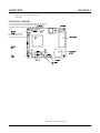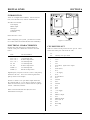
1
RPC-220 USER'S MANUAL
REV 1
NOTICE TO USER
Copyr ight 1998 - Re mote P rocessing Cor poration. All
rights reserved. However, any part of this document
may be reproduc ed with Remote Proce ssing cited as the
source.
The infor mation co ntained in this m anual is believe d to
be correct. However, Remote Pr ocessing assumes no
respons ibility for any o f the softwar e or cir cuits
described herein, conveys no license under any patent or
other r ight, a nd make no repr esentations that the circuits
are free from patent infringement. Rem ote Processing
makes no representation or warranty that such
applications will be suitable for the use specified without
further testing or modification. The user m ust make the
final determination as to fitness for a particular use.
The con tents of this ma nual and the sp ecifications her ein
may change without notice.
TRADEMARKS
Signetics is a registered trademark of Phillips
Semiconductor s.
Remote Pr ocessing Corporation' s general policy does not
recommend the use of its products in life support
applications where the failure or malfunction of a
component m ay directly threaten life or injury. It is a
Condition of Sale that the user of Remote Processing
products in life support applications assum es all the risk
of such use and indemn ifies Remote Pr ocessing against
all damages.
PC SmartLINK® is a trademark of Octagon Systems
Corpor ation.
Intel is a copyright of Intel Corpora tion.
Windows, Windows 95, and Windows Terminal are
trademarks of M icroSoft Corporation.
Remo te Pro cessing is a r egistered tradem ark of R emote
Processing Cor poration.
FCC NOTICE
The RPC-220 was not tested for EMI radiation. When
operated outside a suitable enclosure, the board and any
cables coming from the board w ill radiate harmful
signals which interfere with consumer and industrial
radio fr equencies. It is your r esponsibility to pr operly
shield the RPC-220 and cables coming from it to prevent
such interference.
Remote Processing® Corporation
79 75 E. Harvard Ave.
Denver, Co 802 31 USA
T el: (3 0 3 ) 6 9 0 - 1 5 8 8
Fa x: (3 0 3 ) 6 9 0 - 1 8 7 5
email: getinfo3@rp3. com
internet: www .rp3. com
P/N 1736
Revision: 1.4
Page i
TABLE OF CONTENTS
OVERVIEW
SECTION
MANUAL ORGANIZATION . . . . . . . . . . . .
80C552 INFORMATION . . . . . . . . . . . . . . .
RTC INFORMATION . . . . . . . . . . . . . . . . .
MANUAL CONVENTIONS . . . . . . . . . . . . .
Connector Or ientation and Numbering
Scheme . . . . . . . . . . . . . . . . . . . . .
Term inology . . . . . . . . . . . . . . . . . . . .
1
1
1
1
1
SETUP AND OPERATION
SECTION
OPERATING PRECAUTIONS . . . . . . . . . . .
EQUIPMENT . . . . . . . . . . . . . . . . . . . . . .
DEVELOPMENT SYSTEM SETUP . . . . . . .
Application Programs . . . . . . . . . . . . . .
DE VE L OPI N G U N DE R W IN D O WS . . . . . . .
FIRST TIME OPERATION . . . . . . . . . . . . .
D O W N LO A D IN G P RO G RA M S . . . . . . . . . .
Download and Run a Demo Program . . . .
TROUBLESHOOTING . . . . . . . . . . . . . . . .
2
1
1
1
1
1
2
2
3
3
WRITING, DEBUGGING AND SAVING
SECTION
OPERATING MODES . . . . . . . . . . . . . . . .
Detailed Description . . . . . . . . . . . . . . .
MEMORY MAPS . . . . . . . . . . . . . . . . . . .
ACCESSING I/O AND RAM . . . . . . . . . . . .
MONITOR ROM . . . . . . . . . . . . . . . . . . . .
Effects of the Monitor on a Program . . . . .
MONITOR COMMANDS . . . . . . . . . . . . . .
Display Comm ands . . . . . . . . . . . . . . . .
Modify Com mands . . . . . . . . . . . . . . . .
Miscellaneous . . . . . . . . . . . . . . . . . . .
SAVING YOUR PROG RAM TO FL ASH . . . .
Saving Proc ess . . . . . . . . . . . . . . . . . .
WRITING CODE FOR UPDATES . . . . . . . .
In-circuit Reprogramm ing . . . . . . . . . . .
WRITING FOR C . . . . . . . . . . . . . . . . . . .
Mem ory M odels . . . . . . . . . . . . . . . . .
Memory U se . . . . . . . . . . . . . . . . . . .
Other Considerations for W riting and
Saving Programs . . . . . . . . . . . . . . .
U S IN G D EM O N ST R AT I ON P R OG R AM S . . .
PROG RAM S LARG ER TH AN 32K . . . . . . . .
A P P LI C AT I ON P R OG R AM S . . . . . . . . . . . .
3
1
1
1
2
2
3
3
3
4
5
7
7
7
7
7
7
8
WATCHDOG TIMER
SECTION 9
OPERATION . . . . . . . . . . . . . . . . . . . . . . 1
USE DURING DEVELOPMENT . . . . . . . . . 1
8
8
8
9
EXTERNAL INTERRUPTS
INT 0 . . . . . . . . . . . . . . . . . . . .
INT 1 . . . . . . . . . . . . . . . . . . . .
APPLICATION PROGRAM . . . . .
SERIAL PORTS
COM 0 . . . . . . . . . . . . . .
Control Lines . . . . . . .
SOFTWARE SERIAL PORT
I 2C BUS . . . . . . . . . . . . . .
SERIAL PORT PIN OUT . .
A P P LI C AT I ON P R OG R AM S
4
1
1
1
2
2
2
.
.
.
.
.
.
.
.
.
.
.
.
.
.
.
.
.
.
.
.
.
.
.
.
.
.
.
.
.
.
.
.
.
.
.
.
SECTION
. . . . . .
. . . . . .
. . . . . .
. . . . . .
. . . . . .
. . . . . .
RAM
ACCESSING RAM . . . . . .
BATTERY BACKUP . . . . .
RAM SIZE JUMPER . . . . .
A P P LI C AT I ON P R OG R AM S
2
3
Page ii
SECTION
. . . . . .
. . . . . .
. . . . . .
. . . . . .
5
1
1
1
1
DIGITAL LINES
SECTION
ELECTRICAL CHARACTERISTICS . . . . . .
CPU PORT PIN OUT . . . . . . . . . . . . . . . . .
USING ANALOG INPUTS . . . . . . . . . . . . .
ALTERNATE PIN FUNCTION TABLE . . . . .
6
1
1
2
2
REAL TIME CLOCK
YEAR 2000 . . . . . . . . . . . . . . . .
ADDRESSING . . . . . . . . . . . . . .
PROGRAMMING NOTES . . . . . . .
LOW POWER MODES . . . . . . . . .
Power Down . . . . . . . . . . . . .
Developing in Power D own Mode
IDLE . . . . . . . . . . . . . . . . . .
INTERRUPTS . . . . . . . . . . . . . . .
SQUARE WAVE OUTPUT . . . . . .
OTHER REGISTERS . . . . . . . . . .
EXTERNAL BATTE RY . . . . . . . .
STABILITY AND TEMPE RATURE
A P P LI C AT I ON P R OG R AM S . . . . .
.
.
.
.
.
.
.
SECTION
. . . . . .
. . . . . .
. . . . . .
. . . . . .
. . . . . .
. . . . . .
. . . . . .
. . . . . .
. . . . . .
. . . . . .
. . . . . .
. . . . . .
. . . . . .
7
1
1
1
1
1
1
2
2
2
2
3
3
3
COUNTE R/TIMERS
TIMER 0 . . . . . . . . . . . . .
J3 CONNECTOR PIN OUT .
TIMER 2 . . . . . . . . . . . . .
A P P LI C AT I ON P R OG R AM S
.
.
.
.
SECTION
. . . . . .
. . . . . .
. . . . . .
. . . . . .
8
1
1
2
2
.
.
.
.
.
.
.
.
.
.
.
.
.
.
.
.
.
.
.
.
.
.
.
.
.
.
.
.
.
.
.
.
.
.
.
.
.
.
.
.
.
.
.
.
.
.
.
.
.
SECT ION 10
. . . . . . . 1
. . . . . . . 1
. . . . . . . 1
TABLE OF CONTENTS
ANALOG INPUT
SECT ION 11
CONNECTING ANALOG INPUTS . . . . . . . . 1
ACQUIRING ANALOG DATA . . . . . . . . . . 1
INPUT SIGNAL CONSIDERATIONS . . . . . . 1
Slew Ra te . . . . . . . . . . . . . . . . . . . . . . 1
Signal Source . . . . . . . . . . . . . . . . . . . 1
EXTERNAL TRIGGER . . . . . . . . . . . . . . . . 2
NOISE . . . . . . . . . . . . . . . . . . . . . . . . . . . 2
MEASURING HIGHER VOLTAGES . . . . . . . 2
Measuring 4-20 mA Curre nt Loops . . . . . 2
CALIBRATION . . . . . . . . . . . . . . . . . . . . . 3
A P P LI C AT I ON P R OG R AM S . . . . . . . . . . . . 3
J1 ANALOG I/O CONNECTOR PIN OUT . . . 3
PWM AND ANALOG OUTPUT
SECT ION 12
PR OGRAMM IN G P WM . . . . . . . . . . . . . . . 1
Quick P WM Prog ram ming E xample . . . . . 1
ANALOG OUTPUTS . . . . . . . . . . . . . . . . . 1
Response Time . . . . . . . . . . . . . . . . . . 1
Measuring outputs using on card A-D . . . . 2
Output levels and noise . . . . . . . . . . . . . 2
PIN OUTS AND REGISTER INFORMATION . 2
DISPLAY PORT
SECT ION 13
PIN OUTS . . . . . . . . . . . . . . . . . . . . . . . . 1
Connector Or ientation . . . . . . . . . . . . . . 1
CONTRAST/ANGLE ADJUSTMENT . . . . . . 1
APPLICATION PROGRAM . . . . . . . . . . . . 2
EXPANSION PORT AND POWER
EXPANSION PORT . . . . .
EXTERNAL POWER . . . .
Heat Sink . . . . . . . . .
LOW POWER MODES . . .
Expansion Port Pin Out
.
.
.
.
.
.
.
.
.
.
.
.
.
.
.
.
.
.
.
.
.
.
.
.
.
.
.
.
.
.
SECT ION 14
. . . . . . . 1
. . . . . . . 1
. . . . . . . 1
. . . . . . . 2
. . . . . . . 2
TECHNICAL SPECIFICATIONS
SECT ION 15
MECHANICAL . . . . . . . . . . . . . . . . . . . . . 2
MOUNT ING TO A MOTH ER BOARD . . . . . 2
Connector Positions . . . . . . . . . . . . . . . 3
Page iii
OVERVIEW
SECTION 1
DESCRIPTION
MANUAL ORGANIZATION
OVERVIEW
SECTION 1
The RPC-220 is a small embedded controller
program mable in C or assembly. Included is a monitor
to facilitate program downloading and debug.
Program ming is usually done on a PC using any 8051
compatible assembler or C compiler. Additional
hardware features include:
!
!
!
!
!
!
!
!
!
!
This manual, along with the application disk, provides
information to write C code and download it to the card.
Softwar e exam ples use the D unfield M icro-C , bu t should
be adaptable to any other softw are vendor s.
Each chapter has one or more ready-to-run program
showing how to use a feature. Wr iting your program
should be a simple matter of combining parts of
program s into your own. T he RPC-220 pr ogramm ing
disk has both source code a nd output for all exam ples.
Sample programs run stand alone, meaning there is some
measur ement an d display going o n or an ou tput.
On car d flash EP ROM allows pr ogram updates in
the field without remo ving any parts.
LCD charac ter por t with contr ast adjustme nt. A
keypad may also be connected.
Second software serial port
Watchdog timer resets card
Ni ne te e n + i nd iv id u ally p ro g rammab le d ig ital I/O
lines
Two P WM outputs (shared with analog o utputs)
Eight channel, 10 bit resolution A-D converter
T wo an a lo g ou tp u ts (s hared w ith P W M )
Real time clock with inte rrup ts
Low power modes and wide input voltages
This manual assumes you are fam iliar with 8051 C
and/or assembly language. If you are not experienced
with C, you may want to refer to books and training
programs available through many colleges. The C
compiler vendor you are using to develop progr ams w ill
have program ming information specific to the 8051.
80C552 INFORMATION
There are several PDF files which have detailed
information about the 80C552 CPU. These files are
viewed us ing a PD F re ader suc h as Adob e Acr obat,
version 2.1 or 3 or later. You m ay print these out to get
more inform ation as they are referred to frequently.
The RPC-220 uses a Phillips 80C552 CPU operating at
22.1184 M hz. T his CPU is software com patible with the
Intel 8051 series of CP Us.
A monitor is standard with the flash. The m onitor
facilitates program development and, w hen development
is complete can be replaced by the final program. The
ROM can also be replaced by other third party software
interfacing to debugging software.
8XC552OV.PDF
80C552X .PD F
FAMHDWR.PDF
PR O G GU I.PD F
AN418.PDF
93017.PDF
The RP C-220 is available in 3 differe nt models.
P /N
Description
1710
Full featured with 512K battery backed
RAM , rea l time clock, 32K flash type
EPROM , 10 bit, 8 channel A-D, 2 channel
D-A (derived from PWM signal),
counter/timers. Low power mode draws
less than 5 ma. 5. 0/5.4 to 21 volt power
input without a heat sink. Operating
current is about 90 ma.
Program ming information.
Electrical information for the
80C552. This is a subset of
FA M H D W R .PD F.
80C51 hardwa re information.
80C51 programming guide.
83C552 timer 2 application note.
8XC552 analog input application
note.
NOTE: Ther e is an err or in the 8X C552O V. PDF data
file. Figures 6 and 7 are in error. The RTE
register in Figure 6 resets bits P4. 0 to P4.5 on a
match to C M1, not CM 2. T he STE register in
Figur e 7 sets bits P4. 0 to P4. 5 on a ma tch to
CM1, not CM2.
RTC INFORMATION
1715
Similar to P/N 1710 except RAM is 128K.
Low power mode is 40 ma. Operating
current is about 150 ma.
1720
Low cost version. No clock, battery
backup, analog output, or reset switch.
The optional real time clock file is 1689-93.PDF. As
with the 80C552 information, these are read and printed
using a PDF reader.
Page 1-1
OVERVIEW
SECTION 1
MANUAL CONVENTIONS
Information appearing on your screen is shown in a
different type. Exam ple:
Remote Pr ocessing Debug Monitor
For RP C-220
Version 1. 0
Type ' H' for command sum mary
26 Pin Connector P in Out
NOTE:
Text unde r this headin g is helpful infor mation. It is
intended to act as a reminder of some operation or
interaction with another device that may not be obvious.
Counting scheme is the same fo r 10, 16, and 20 pin
connectors.
Terminology
"A-D"
Shorthand for analog-to-digital converter. The A -D
"measures" a voltage and converts it into a binary
numbe r. On the RP C-220, this numbe r is from 0 to
1023.
WARNING:
Information under this heading warns you of situations
which might cause catastrophic or irreversible damage.
Wx[a-b]
Denotes jumper block pins. [a-b] ar e the
pins to connec t.
" f la sh E PR O M "
Technically, the EPRO M used in the RP C-220 is a
PER OM . U nlike a flash, a sector d oes not have to
be erased before written to. Unlike an EEPROM
(electrically erasable PROM), 64 bytes are written
at a time. EPROM, flash, and flash EPROM are
used interc hangeably in this manua l.
< xxx> Paired angle brackets are used to indicate a
specific function key on your PC keyboard. For
example < esc> means the escape key.
Jx-N
Designates a pin number on a connector.
' C' convention ge nerally use s hexadecim al to designate
addresses and decimal for data. Any hexadecimal
numbers are r epresented by standard 0xNN notation.
Decimal does not have any special notation.
"MOVX"
refer s to the 8051 asse mbly lang uage instru ction to
read or write to external memory. This manual uses
the te rm to refe r to a ny e xte rna l R A M or I / O
access.
Connector Orientation and Numbering Scheme
The RP C-220 uses ID C type (0. 1" center ) connectors.
Shrouded conn ectors are ke yed to protect against rev erse
installation. They also take up a lot of room. The RPC220 has silk screen marks on the board to indicate the
key on the co nnector . P ins 1 and 2 ar e indicated on a ll
of the larger co nnectors.
"I/O"
are input- output devices . O n the RP C-220, this
includes the RTC, expansion port, RA M segment
set, and flash EPRO M. I/O is an accessing mode
enabled w hen CP U por t P4. 0 is low. When n ot in
the I/O mode, external RAM is selected.
IDC type connectors (J1-5) follow a pin out numbering
scheme shown below. View is component side. Square
pad (pin 1) is found on the circuit side.
"RTC"
is the optional real time clock in U8.
"segm ent"
is a 64K block of RAM . U p to 8 segments,
numbered 0 - 7, are available. The 8051 CPU series
accesses RAM in 64K blocks. The limitation is due
to the limited number of address lines. The
RPC -220 bank switches RA M in 64K segm ents.
Page 1-2
OVERVIEW
SECTION 1
This pr actice is com mon am ong 8 bit
controllers.
TECHNICAL SUPPORT
If you have a question about the RPC-220 and can' t find
it in this manua l, ca ll us and ask for technical supp ort.
Technic al suppor t hours ar e 9 AM to 4 PM mountain
time.
Phone: 303-690-1588
FAX : 303-690-1875
email: info@rem otep.com
RPC-220 C omponent Location
Page 1-3
SETUP AND OPERATION
SECTION 2
INTRODUCTION
You can install the C compiler at any time.
SETUP AND OPERATION
SECTION 2
The RPC-220 is ready as soon as you connect it to a PC
and apply power. This section describes what is needed
to get a sign on m essage. A dem onstration p rogr am w ill
also be downloaded.
You m ay want to pu t in the stand-offs to the board. This
keeps the board from touching metal or other surfaces
where the battery could discharge.
"Developm ent System Setup" describes hooking up using
components from our development system.
Refer to Figure 2-1 on the next page. Connect the
power cable assembly (P/ N 1725) to "Pow er In" on the
board. The R ED w ire goe s to P1 te rmina l mar ked "V".
B la c k goes to P1 termina l ma rke d "G".
OPERATING PRECAUTIONS
The RPC-220 is designed to handle a wide temperature
ranges at low power. These characteristics require using
CM OS com ponents. CM OS is static sensitive . T o avoid
damaging these components, obser ve the following
precautions:
1.
2.
Ground yourself before handling the RPC -220 or
plugging in cables. Static electricity can easily arc
through cables and to the card. Simply touching
your P C befor e you touch the card ca n greatly
reduce the amount of static.
Do not insert or remove cables or components when
power is applied.
EQUIPMENT
You will need the following equipment to begin using the
RPC-220. If you ordered the development system, the
' !' items are supplied.
!RPC-220 embedded controller
!VTC -9F ser ial cable
!Power supply, 6 to 15 VDC @ 300 m a or
+ 5, 300 ma
PC with a serial port and communications program
(such as Microsoft Windows Terminal or Procomm)
Refer to SECT ION 4, "SERIA L POR T PIN O UT" , for
wiring information to make your own serial cable.
The application disk is necessary to run the
demonstration program . This disk is included in the
development system.
DEVELOPMENT SYSTEM SETUP
A development system has most of the software and
hardware neede d to get your card operating. A ll you
really need is a PC with a serial port and a serial
communications program. A development system
includes terminal boar ds with cables to easily access
analog and digital I/O.
You m ay plug the pow er supply into a 120 VA C wa ll
outlet or power strip. Power may be applied or removed
from the RPC-220 board by plugging the 3.5mm
connector from the power supply to the pow er cable
assembly.
Continue with "Fir st Time Operation" below. Since the
power supply is set up, skip step 1.
Application Programs
To use the application and demonstration programs, you
must put them to your hard drive first. They can be any
place you want. Make up a subdirectory and run 'RPC200.BAT ' to extract the files. This program expands
files in the current DOS directory and creates additional
subdirectories.
DEVELOPING UNDER WINDOWS
You can write, compile, and debug under Microsoft
Windows 95 or NT. An easy way is to create a folder
and put your editor (Word, Wordpad, Note pad, or
other), terminal program, and MS-DOS icon in it. Open
the editor a nd term inal progr ams and use the task bar to
switch between the two.
The Windows ' Terminal' program configuration file,
mon220. trm, is supplied on the applications disk. You
may nee d to change the COM port.
MS-DOS properties are changed to invoke the compiler.
(Properties are selected by first right clicking on the MSDOS icon). ' Cmd line:' box is changed to:
C:\mc\CC51 \rpc220\subdir\fname.c -p -i
' subdir' is the directory you are writing your program
in. ' fname.c' is the file you are compiling. Additional
command line options, such as ' -p -i' , are at the end.
The ' Working:' directory is nearly the same:
c:\rpc220\subdir
Page 2-1
SETUP AND OPERATION
SECTION 2
An inconvenience using some of the Microsoft Windows
editors is a lack of line number indication. Should you
ever make an er ror wr iting C code, the compiler r eturns
the line numbers of the error(s). Using a DOS editor,
such as "Edit", you can quickly go to the offending line.
Wordp ad or No tepad do not show you line num bers.
Wor d indicates the line on a page. Also, Wor d tends to
leave the file it is editing open. When it is open, the
compiler cannot access it. You will need to save and
close the file before compiling. Wordpad or Notepad do
not have this problem.
FIRST TIME OPERATION
Become familiar with the locations of connectors before
getting started. See Figure 2-1. RPC-220 jumpe rs have
been set at the fa ctory to op erate the system im mediately
using a 6 - 21 V supply. If you have a
5V supply, then remove jumper W4. For first time
operation, do not install any connectors or parts unless
specified belo w. Jumper s should be kep t in default
positions.
1.
Figure 2-1 Start up connector locations
2.
Connect power.
The RPC -220 needs + 5 volts or 7 to 21 volts at 300
ma. T he RPC-220 has its own regulator which
supplies 5V to the rest of the card w hen powe r is
applied to the ' V' termin al.
Connect the ser ial ports.
Connect one end of the VTC -9F connector to the 10
pin ' COM ' port (J4) on the RPC-220. The VTC -9F
' key' on the 10 pin connector faces the inside of the
card. Refer to Figure 2-1 for connector location.
Connect the DB-9 end to the PC's COM1 or COM2
port. You m ay need a 9 p in male to 25 pin female
adapter . T he VT C-9F is designed to plug directly
into the 9 pin serial port connector on a PC.
Start up your serial communication program. Set
comm unication par ameter s to 19200 bau d, 8 data
bits, no parity, 1 stop. If using Microsoft Windows
Ter minal, you may load up ' mon220 .tr m' file
(located on the applications disk r oot directo ry) to
quickly configure the program. M ake sure you set
the "connector" to C OM1 or COM 2 in the
Communications window.
Be careful when using "switching" power supp lies.
Some supplies do not regulate properly unless they
are adequately loaded.
Make sure pow er is off. Conne ct the powe r supply
to one of the appropriately marked terminals on the
RPC-220. Power connector P1 is designated as '5'
for 5 volts, ' V' for the 6-21 volt input, and ' G' for
ground.
3.
Power up.
Turn on or connect the power supply. On power up
a message is printed.
Remote Processing Debug Monitor
For RPC-220
Version 1.0
If a nonsense message appears, your terminal or PC
may not be set to the appropriate communication
parameters. If the system still does not respond,
refer to TRO UBLESH OOTIN G later in this section.
4.
Page 2-2
Testing.
Press the "Enter" key on your PC to verify the '> '
symbol returns. Type the letter "h" to view the
monitor help menu. If the system responds, you are
SETUP AND OPERATION
SECTION 2
now ready to send a program.
DOWNLOADING PROGRAMS
When d ownloadin g progr ams, select ASC II text form at.
XMO DEM , YM ODE M or other for mats are not used.
Transfers ar e done a line at a time. The pacing
character is '> '. A delay is not necessary. Programs
genera ted by the assem bler or compiler should be in
standard Intel hex format. E xtended addressing records
are ignored.
Page 2-3
SETUP AND OPERATION
SECTION 2
supplies 5 volts fr om an ex ternal sour ce. If this is
below 4.65 volts at the input power terminal, the
RPC-220 is in reset. Power is 5 ±0.25 volts. Make
sure the 5V supply goes to the pin marked '5' on P1
terminal strip.
Download and R un a Demo Progr am
The file "demo.hex", should be in the root directory
wher e you put the de monstr ation prog ram s. T his
program displays digital status at J3 and voltage inputs at
J1.
Make sure jum per W4 is rem oved if using a 5V
supply and installed for higher voltages (using the
regulator). D efault is jumper is installed.
To download the program, prepare the RPC -220 for hex
download by simply typing
Make sure the 5 volt supply is "clean". If it dips
intermittently to 4. 65 volts (due to switching noise
or ripple), the car d will reset for about 100 ms. If
the noise is fre quent enoug h, the card w ill be in
perm anent re set. C heck the cen ter pin on U 7. If it is
low, then the card is in reset. This line should be
high (about 5 volts). Some switching power supplies
require a minimum load to operate. Check your
power supply specifications. The RPC-220 draws
from 80 to 140 m a, d epending up on the mo del.
R< Enter>
' R' is the hex download command. The monitor
automatically converts lower case to upper case.
After y ou have hit the < Enter > key, you are ready to
send a text file. How this is done depends upon the
terminal pr ogram you are using. For m ost terminals,
this is a simple ASCII transfer. Refer to SECTIO N 3,
MON ITOR CO MM ANDS, Miscellaneous, R Read Intel
Hex F ile for setup inform ation on different prog rams.
The second option supplies 6 to 21 volts from an
external source. Power is applied to P1 terminal
marked ' E' . Ver ify the voltage at P1-3 (terminal
marked ' 5' ) is between 4.75 and 5. 25 volts. If the
voltage is missing, verify jumper W 4 is installed.
Make sure the supply voltage is relatively clean. It
may have some ripple on it, pr ovided it does not go
below 6 volts. Make sure you are not using an AC
power source.
For Window s Ter minal, select ' Transfers' , then ' Send
Text File'. Select "DEMO.HEX". Appending a LF
after the C R is optional.
Downloading takes about a minute.
After download, type in:
G 8000
2.
The program will execute starting at address 0x8000.
You should see a continuous display of analog input and
digital I/O status. At this point you can connect the
STB-20 terminal board to the analog connector J1.
Apply a battery or other < 5 volt input to one of the
channels and you should see the result. Use the STB-26
terminal boar d for J3 CP U port to chang e port status.
Refer to SECT ION 6, DIGITA L LINE S, Table 6-1 for
pin outs. You may bring the a line high or low and see
the result on the scree n. T he port statu s in hex is
displayed.
Remove the connector from COM 0. Refer to the
outline drawing earlier in this section. Connect an
oscilloscope (preferred) or a voltmeter to pin 3
(Txd) and ground. Pin 3 should be -6 volts or more
negative. (Pin 1 and pin 2 are mar ked on the
board). Pin 3 is next to pin 1. If y ou have -6 vo lts
or more, reset the board. If you have a scope
attached, you should see a burst of activity. With a
volt meter, you should see a change in voltage.
Using a Fluke 8060A set to measure A C, you
should see a mom entary rea ding above 2 volts.
TROUBLESHOOTING
You would probably came to this section because you
could not get the sign on message. If you are getting a
sign on message but can' t enter characters, then read 5
in this section. The follow ing are tr oubleshooting hints
when you can' t get anything.
1.
Check the COM 0 port (J4).
Make sure the VTC-9F serial cable is oriented
correctly. The key on the cable corresponds to a
silk screen area on the board.
3.
Check the power source.
There are tw o board power options. The first one
Page 2-4
Check
Install
output
on the
the cable.
the cable and make sure the voltages and
activity are still there. Output is from pin 3
VTC-9F. If not, check to make sure
SETUP AND OPERATION
SECTION 2
something is not shorting th e output. Wiring is
in SECTION 4, SERIAL PORT PIN OUT.
4.
Check the serial parameters on your PC.
T h ey sh o ul d b e set to:
19200 baud
No par ity
8 data bits
1 stop
Make sure you have set the comm unications port on
your PC to the one the VTC-9F is plugged into.
5.
Receiving a sign on message and can't enter
character s.
Check U9, pin 14 for at least -6 volts with the serial
cable connected to the PC . W hen it is near 0 volts,
the terminal or PC' s Tx line is not connected. When
you press a character on the terminal or P C, you
should see the voltage go positive on the
oscilloscope.
If all of this fails, call technical sup port listed in
SECT ION 1.
Page 2-5
WRITING, DEBUGGING, AND SAVING PROGRAMS
SECTION 3
EPR OM is accessed as code fro m addr ess 0x0000 to
0x7fff.
INTRODUCTION
WRITING, DEBUGGING AND SAVING SECTION 3
The RP C-220 is p rogr amm ed in C or assembly
languages. Virtually any 8051 type compiler and
assembler may be used to generate code. An assembler
is provided on the application disk. This section
provides information to set up your compiler/ assembler.
The I/O contr ol line complicates things just a bit. The
purpose of this line is to allow access to non-RAM
devices (such as the real time clock and expansion
boards) while still allowing full access to RAM. The
PEE L in U6 controls R AM , I/ O, and flash acc ess. It is
designed to allow code access in the memory map
(Figur e 3-1 below ), R AM and I/O at the same time. This
is how code runs from RA M while accessing the RTC. It
also allows RAM to be modified in the code area.
OPERATING MODES
The RPC-220 executes code in one of two modes called
development and normal. The defining difference
between the two modes is how the memory map
changes. In norm al mode, the C PU accesses its code
from U3 flash EPROM exclusively. All of RAM in U4
is accessed using MOVX type com mands. In
development mode, code is also accessed from RAM
starting at address 0x8000.
Generally, the I/O control and development/normal lines
operate independen tly. T he only time both lines oper ate
together is during flash programming.
MEMORY MAPS
Memor y maps are controlled by one of two bits on the
CPU por t. Port P4. 1 controls development/normal
mode. On power up or reset, this line goes high placing
the board in normal mode. A low configures the board
for development mode.
I/O m ode accesses devices (RTC, expansion port, and
flash EPROM ). This mode is accessed by setting the
I/O bit (CPU port P4.0) low.
During development mode (CPU port P4.1 low), RAM
from address 0x8000 to 0xffff can, but does not have to,
ex ec u te c od e . T his mem ory can be access ed as I/O
using MO VX com mands.
Port P4. 0 selects between RAM and other I/O such as
the RTC, expansion port, and flash EPROM . On power
up or reset, this line goes high allowing access to RAM.
A low maps out the RAM for MO VX type instructions
only. Code c an be acce ssed if the deve lopment m ode is
selected (P4. 1 is low). W hen P4. 0 is low, the flash
eprom, expansion port, and RT C are accessible using
MOV X type comm ands.
When setting up your compiler or assem bler to develop
code, set the ORG (originate) to 8000H. The m onitor
vectors interrupts to base address + 8000H. For
example, when there is a serial interrupt the CPU
vectors to address 0x23. The monitor has a jump
instruction to address 0x8023.
During norm al mode, up to 64K is accessible by making
a PCB modification and replacing U3 with a 27C512
type EPROM. As delivered, 32K of code is accessible.
See Program s larger than 32K later in this section.
When you are done w riting code, simply change the
ORG to address 0 and re-compile or assemble.
Detailed Description
Development/nor mal and I/O m odes are controlled by
two lines dir ectly from the CP U. On pow er up or reset,
these lines go high, placing the card in normal operating
mode capable of accessing external RAM. When the
DEV L line (por t P4. 1) goes low , the card is in
development mode. When the I/O line (port P4.0) goes
low, non-RAM devices are accessed. These lines are
mutually exclusive, except when pr ogram ming the flash
E P R OM .
The mem ory map changes, depending upon the status of
the development and I/O control lines. Figure 3-1 shows
the code map during development mode.
Development mode sim ply allows CPU code to be
accessed from RAM at addresses 0x8000 to 0xffff.
MOVX type commands always access all of RAM
(assuming the I/ O control line is high). U3 flash
Figure 3-1 Code Memor y Map
Page 3-1
WRITING, DEBUGGING, AND SAVING PROGRAMS
SECTION 3
NOTE: The I/O contr ol line, CPU port P. 0, should be
low for as short a period of time as possible.
Additionally, interrupts should be turned off
while the line is low especially if the routine
accesses external memory. The following are
suggested step s to using the I/ O por t.
Code starting at 0x8000 should be exactly what you
would have if you were starting in EPRO M at address 0,
except there is an 0x8000 offset. Interrupts are handled
by the monitor by jumping to 0x8000 + interrupt base.
Change your C compiler start up code so it starts at
0x8000. If you ordered the development system, then
the code needed to use the Dunfield compiler has been
included. Simply install the Dunfield compiler first, then
replace the files with those on the supplemental disk.
These files are 8051RLPT .ASM , 8051RL PM. ASM, and
8 05 1R L P L. A S M .
1
2
3
4
5
6
The I/O map is more complicated because there are
more de vices to select. A ll I/O is accessible re gardless
of the setting of the d evelopm ent/no rma l mode bit.
Figure 3-2 is the external map.
Set up pointers and registers as necessary to perform
the I/O operation.
Turn off interrupts (if used)
Set CPU por t P4.0 low
Per form the read o r wr ite
Set CPU por t 4.0 back high
Enable interr upts.
Step 4 above may c onsist of several reads a nd/or writes.
The idea is to keep this time short.
Altern ately, you could w rite inter rupt ser vice routin es to
check the I/O line before accessing RAM . The line
would be r estored a fter ser vicing. The r eason this
method is not recommended is the amount of time
needed to read, store, and restore the status is longer
than the time it takes to code str aight throu gh. If step is
4 long (say monitoring a clock status bit), perhaps the
extra ove rhead m ight be wor th it.
Se e the M EM 220.C progra m to se e how RA M and I/ O
are accessed. Specialized speek and spoke functions are
written in assembly language. This wa s done not only to
speed up memory access and reduce interrupt off time
but to ensure correct access. N ote that parameters to the
function are passed in the stack and returned in registers
A and B. Make sure your compiler passes parameters
through the stack in the memory model you are using.
You may have to adjust parameter passing for your
compiler.
Figure 3-2 I/O and RAM Map
Ea ch a re a is se le c ted by th e fo llow ing tab le:
Device/area
Flash EPROM
Expansion port
Real time clock (RTC)
RAM segment
Address
0x0000
0x8000
0xa000
0xc000
-
0x7fff
0x9fff
0xbfff
0xffff
MONITOR ROM
Several demonstration programs access I/O. Directories
where progr ams are located:
The monitor ROM allows you to download code, set
breakpoints, exam ine and modify RAM and I/ O. T he
monitor occupies the same space as the final program
will. Generally, the final code replaces the
monitor when the project is done. T he monitor can be
re-installed under tw o conditions:
MEM 220
RTC
FLA SH
ACCESSING I/O AND RAM
I/O dev ices and RAM share the sam e addresses. Access
to them is controlled by CPU port P 4.0. When this line
is high, RA M is accessed using M OVX type comm ands.
When this line is low, the expansion port and real time
clock are accessed.
Page 3-2
1
Your code allows the flash to be written to. This is a
routine that must be included in your program. See
"SA V IN G Y O U R PR O G RA M TO FLA SH".
2
The flash is removed from the socket and
programmed using an external programmer.
WRITING, DEBUGGING, AND SAVING PROGRAMS
SECTION 3
' H' or ' ?' is entered.
Monitor source code and hex file are under the MON 220
directory.
All num eric data is entered a s HEX . A n addre ss is up to
4 bytes long. Any address less than this assumes leading
0' s.
Some internal registers and ports are initialized upon
power up and program break. These include registers
associated with CO M0, RAM segment, and timers.
A partial list of modified registers include: S0CON,
TM OD, TCO N, TL1, TH1 and all of the r egisters in
bank 0. Review the source code, under the programs
"M AIN220. ASM" and "STA RT220. ASM" to determine
which registers are used and how they might affect your
code.
Pressing the < esc> key at any time aborts a command.
Comm ands with parameters in [brackets] are optional. If
nothing entered, 0 is assumed for that and any rem aining
parameters. For example, if an address and segment are
parameters of a com mand but nothing is entered for
either, then 0 is assumed for both.
External RAM from address 0x7fc0 to 0x7fff are used
by the monitor to store break points and registers. M ake
sure your progr am does not write in this area if you
intend to use these.
Comm ands with multiple parameters are separated by a
comma (, ).
An Enter (< cr> ) executes a comm and in most cases.
Some commands, such as DI and H, execute as soon as
the key is hit.
Effects of the Monitor on a Program
The m o ni to r pr o gram m in im ally mo difies RAM and I/O
ports during its normal operation. There are some
modifica tions the mon itor does to op erate. These ef fects
are most noticea ble during brea ks.
Display Commands
There a re 5 display com mands:
DX
DI
DP
DR
DS
RAM segment is reset to 0 upon entry. The RAM
examine comm and (DX) tempor arily modifies the
segment during access only.
I/O mode is reset to RAM.
Interrupts are turned off via the IEN. 7 bit in the
interrupt register.
Display eXternal memory
Display Internal memory
Display P ort or I/O d ata
Display Registers
Display Special function registers (80H FFH)
Data is displayed 16 lines at a time (except for registers).
The segm ent, if applicable, followed by the addr ess
starts off a line. Up to 16 bytes of data are displayed,
followed by printable A SCII cha racter s. P rintable
characters are those from 20H - FFH.
The monitor sets its stack to address 0x60.
' register ' or inter nal RAM variables at or abov e this
address may get c orru pted or oth erwise not reliable
using the DI command.
DX D isplay external memory
External mem ory is RAM on the RPC-220 card. It
is accessed using a segment:memory type scheme.
Comm and form at is:
After a reset, the 8051 stack is automatica lly set to
internal address 7. ' register' or internal RAM from
0x08 to 0x0c get modified. The only time this is a
problem is when you reset the card and wa nt to look
at data in this area. To solve this problem in C,
simply declare 4 'dummy' integer registers before
the others.
DX [address[,segment]] <ret>
If DX is simply en tered, the monitor assum es address
and segm ent 0. If an addr ess is entere d but no segm ent,
then segment 0 is assumed.
Ports and registers are r estored for Goto comm ands
except P4.1. This bit controls the development mode and
is always set low on GOTO.
DI Display internal memor y
Internal m emor y is RAM internal to the CPU . It is
fixed at 256 bytes. Comm and form at is:
MONITOR COMMANDS
The following describe command function and operation
in greater detail. The m onitor displays a summary when
Page 3-3
WRITING, DEBUGGING, AND SAVING PROGRAMS
DI
SECTION 3
Special function registers are those between 80H - FFH.
These include timers, A and B accumulators, P SW, and
other register s. Since ther e are only 128 locations, 8
lines are displayed. This command is different from DR
in that the current contents is displayed. DR show s those
saved after a break or
reset.
All internal memory fr om 0 to FF H are displayed.
DP D isplay I/O port
Addresses for I/O devices (and monitor EPROM)
are show n in the I/O mem ory m ap above. This
comm and autom atically sets the I/ O contr ol CP U bit
P4 . 0 . T he DP co m man d is us ed to access I/O
devices (RTC , expa nsion). C omma nd forma t is:
NOTE: A short pr ogram is run from RAM at address
0xfffa to directly access these registers. You
may have to reload your program after
executing this command.
DP address<cr>
You can view the contents of the monitor EPROM
in U3 using this command. T he address is from 0
to 0x7fff.
Modify Commands
There are 4 com mands to modify mem ory, r egisters, or
I/O:
DR D isplay Registers
CPU registers A, B, R0-R7, DPTR, CPU ports P1
and P3, stack pointer (SP), program status word
(PS), interrupt (IE), and program counter (PC) are
displayed. These registers are displayed after a
program break is encountered and are loaded on a
GOTO command.
MX
MI
MS
MO
Modify
Modify
Modify
M odify
eXternal memory
Internal memory
Special function registers
I/O
Data or status to be mo dified is displayed one byte at a
time. The mem ory segment, if appropriate, is displayed
at the start of the line followed by its address. The
current data is then displayed. If the data is modified or
skipped (by pressing the space bar), the next address and
its data is displayed. A max imum of 4 addr esses and data
are displayed on a line.
When using this com mand after a power up or push
button reset, certain registers default to a variety of
states. The SP is always 7, DPTR and PSW (PS) are
0. P1 and P 3 are set to a state that forces bank 0 and
memory segment. Additionally, the PC (program
counter) is not valid. Comm and format is simply:
For ex ample, MX c an display the following at address
0x0000:
DR
00:0000 0A
The term inal outputs:
A B R0 R1 R2 R3 R4 R5 R6 R7 P1 P3 PS SP DPTR IE PC
12 34 56 78 9A BC DE F0 12 34 C7 CE 04 4E 0123 00 2114
Number s under the registers are for illustration only.
Upon reset or program break, register values are stored
in external RAM. Register values after reset reflect
default conditions. PC is not reliable and IE is always 0.
Registers may be modified using the MX com mand. The
starting address is displayed on a break command.
0001 0D 03
0002 52 43
0003 43 51
Segment:addr ess is first displayed followed by the
current data at that address. If < space> is hit, nothing
is modified and the next address and data are displayed.
To modify, simply enter the new value.
Addresses and data are displayed in hex notation.
Modifications are entered in hex.
Data is modified or not modified depending upon the
number of data character s entered, if any, and type of
continuation character hit. Pressing < space> always
continues to the next address. If any characters were
entered, then data at the address displayed gets modified
by the value displayed. If no characters were enter ed,
then no modifications are made. Pressing < Enter>
ends the modification routine. If any digits were
entered, then data at the last address is modified.
DS Display SF R' s
Special function registers are accessed by the DS
comm and. F ormat is:
DS
A < cr> is not necessary.
Page 3-4
WRITING, DEBUGGING, AND SAVING PROGRAMS
SECTION 3
16 bit address. A record type 04, extended linear
address recor d, d oes not pro duce an er ror b ut is
ignored. Any RAM memory from 0 to FFFF H may
be loaded to. The com mand for mat is:
MX M odify external memory
Exter nal mem ory is RA M on the RPC card. It is
accessed using a segment:memory type scheme.
Comm and form at is:
R [offset]
MX [address[,segment]] <ret>
' offset' is any value fr om 0 to F FF FH . ' offset' is
added to the a ddress in the hex file. Data is stor ed to
offset + address. Use offset when you want to load
code starting at another address. Keep in mind that
any addr ess loaded be tween 0 an d 0x7F FF is kept in
externa l RAM and is not acce ssible as code. Data
loaded between 0x8000 and 0xFFFF is accessible as
either code or data.
MI M odify internal memory
Internal memor y is the RAM internal to the CPU . It
is fixed at 256 bytes. C omma nd forma t is:
MI [address]
If an address is not entered, 0 is assumed.
MP Modify I/ O ports
I/O dev ices such as real time cloc k, digital por ts,
D-A converter s, counters, etc. are m odified using
this command . F ormat is:
If a checksum error is received during a download,
the last address stored is printed on the screen along
with a prompt to press the < esc> key to stop
printing the message.
MP [address]
Downloading code is done using any number of
modem communication programs. This includes PC
SmartLink, Procomm, and Windows Terminal. No
matter w hich comm unication progra m you use, first
type the letter "R" followed by the offset, if any. No
value entered assumes a 0. T he monitor is now
waiting for a ":" to begin processing a line. After a
line is sent, the monitor returns a "> " character as
a pacing prompt. If there is an error in the
checksum , the progr am w ill continuously sen d out a
message until the < esc> key is pressed.
Instructions for three communication programs are
given below.
If an addr ess is not enter ed, 0 is assume d for both
param eters.
MS M odify Special Function R egisters
The 80C 552 has several special func tion registers.
They are accessed in the range of 80H to FFH.
Refer to the Phillips da ta sheet (file
8XC552OV .P DF) for register specific information.
Comm and form at is:
MS [address]
When [address] is not entered, 0 is assumed. The
monitor pr ogram does not check addr esses.
Procomm
Make sure P rocomm ' s ASCII download is set up
using a "> " as a pacing character. Delays between
characters and lines are not necessary. Select
Upload a nd then AS CII as the type. Enter the file
name the n < Enter > . Y ou will see the H ex file as it
is sent.
Miscellaneous
F Fill External Memory
External mem ory is filled with a value. Comm and
format is:
F start_address,end_address,value[,segment]
Window s Ter minal
Under the "Settings" menu selection, make sure
"Text Tr ansfers" are set to "L ine at a time" and
under "T ransfer a line at a time" is set to "Wait for
Prompt String". The prompt string is the "> "
character . T o download the file, select "Tr ansfers"
then "Se nd text file" . Se lect the file you w ish to
transfer. The "Strip LF " option can be checked off
to see what is transferred.
' start_address' must be lower than ' end_address' .
Failure to do this will cause most of memory to be
written. A ddress values are not checked.
R Read Intel Hex file
Code and data files are downloaded using the Intel
MCS-86 object format, comm only known as Intel
Hex. This for mat suppo rts both 16- a nd 32-bit
extended addresses. This m onitor supports only the
Page 3-5
WRITING, DEBUGGING, AND SAVING PROGRAMS
SECTION 3
occurred is also displayed. RAM at the break point
address is not restor ed until a ' B number ' is
executed.
If the download pr ocess gets stuck, y ou can press
the < esc> key at any tim e after the download is
aborted. Y ou can also press the reset button.
Pressing the < esc> key at any time during the
download pr ocess aborts the re ceiving process.
As a general rule, external memory is not affected
by a push button reset or break point. Thus, if your
program hangs up you may restore a break point
and replace it at a new address. T he following
illustrates an example. Suppose your code begins as
8000H and you want to set break points at 8112H
and 8215H. Execute the following com mands:
G GOTO Run Program
Once a program is downloaded into RAM and
breakpoints are optionally set, it is executed using
the 'G ' command. T he application program has
complete control. The only w ay to stop exec ution is
to press the reset sw itch or the progr am hits a
breakpoint. Comm and syntax is:
B 0, 8112
B 1, 8215
G 8000
G [address]
When the code at either 8112H or 8215H is reached, the
break point message is displayed.
When GO TO is executed, r egister values from the
last break or reset are loaded first. T hen the
program is executed. This way you can stop
program execution, examine registers, and continue.
Register s may be modified b efore e xecuting. This is
done using the MX command. Register values are
stored beginning at the address shown when a Break
is executed. Values are stored in the same order as
they are displayed.
**Break Register information at address 7FC0
A B R0 R1 R2 R3 R4 R5 R6 R7 PS SP DPTR PC
03 00 98 00 00 00 00 00 00 21 41 4F 2147 2112
Both breakpoints are still active. To continue execution
from this point you must enter:
B 0
Using G into an interrupt section may be tricky,
depending upon its type. The problem is when
interrupts are re-enabled, it may execute the same
program you executed a break. Unless your program
is recursive, variables may be unreliable.
You m ay then enter a new br eak point or ' G 2112' to
continue.
When a break point is set, 3 bytes from the original
program is stored in RAM. Additionally, the break
address is also stored.
B Set / C lear Bre akpoint
A program may be interrupted and the contents of
certain register s displayed when a specified addr ess
is reached. Up to 8 breakpoints, numbered 0-7, are
allowed. Comm and syntax is:
When a progr am break is executed, certain registers and
I/O conditions are set to a known state. See "REGISTER
USAGE AND INITIALIZATION" above for more
information. Y ou may modify these registers using the
MX comm and. Values for registers are in order as
displayed abo ve. The star ting addre ss for the r egisters is
displayed when a break is encountered. T he above
examples is 7FC0.
B number[,address]
number is from 0 to 7. A num ber larger than 7
aborts the command. If address is 0 or left out, the
contents of R AM at the brea kpoint num ber is
restored to its original values. This is the same as
clearing a break point.
S Save to flash EPROM
This command is described in detail below.
This com mand w orks by r eplacing 3 by tes in
externa l RAM mem ory at add ress and r eplacing it
with a CALL to the monitor break point handler.
When a break point is encountered, interrupts are
turned off and contents of registers A, B, DPTR,
P1, P3, P SW, SP, and R 0-R7 are saved and
displayed. Additionally, the address where the break
Page 3-6
WRITING, DEBUGGING, AND SAVING PROGRAMS
SECTION 3
Your program is saved to flash EPROM when
development is done or when you wish to make sure a
program works proper ly.
NOTE: The flash E PRO M is pr ogram med in 64 byte
blocks. The saving routine stops when the
length is rea ched. FF ' s are pr ogram med in
locations not specified to round out the block.
Usually, but not alway s, the monitor is replace d. T his
means the save to flash feature will be gone UNLESS
you put it in your program. See "WRITING CODE
FOR U PDA TES" below for taking care of this situation.
NOTE: Since the flash EPROM is programm ed in 64
byte blocks, you should star t on an even by te
boundary. An ' even' boundary is 0xXX00,
0xXX40, 0xXX80, or 0xXXc0.
You can put code or data in a portion of the flash using
the monitor save com mand. Howe ver, if you over write
starting at ad dress 0 to a bout 1900H , the monitor is
effectively destroyed.
WRITING CODE FOR UPDATES
SAVING YOUR PROGRAM TO FLASH
Ther e are tw o ways to field update code . O ne metho d is
listed in the /LOADE R directory. There, a loader
program always resides in memory. You just set a line
low and the loader program is invoked. Programs are
stored starting at address 400H. Review the readme files
for more inform ation.
The ' S' command transfer s the actual prom burning
routine RAM starting at address 0xff00 and executes
from there. M ake sure none of your program is located
in this area.
The second way is to embed a save routine in your code.
This is discussed further below.
While pr ogram ming is in pr ogress, the letter ' P' is
printed for every 512 bytes program med (about 100
milli-seconds). The letter ' V' is printed on the next line
for every 512 bytes verified. If there is a verify error, a
letter ' E' is printed at the 512 byte block it was verifying
and the progr amming p rocess stops.
A sam ple routine in FL ASH \P FL ASH .C is complete
code to prompt the field person to download and burn a
new pr ogram . It r eceives Intel H ex code, puts it to
RAM , uploads the flash burn program into RAM, and
runs it. How you get to this routine is up to you. You
could check a line status or check a password through
the serial port or any number of different mea ns.
After verifying good, code jum ps to address 0. You
may wan t to press reset to simulate pow er on conditions.
In-circuit Reprogramming
The gen eral str ategy is to tem porar ily go into
development mode. The ROM code puts programm ing
code in RAM, sets the development mode bit, and jumps
to it. Sample code is under the "flash" direc tory.
Saving Process
You can use the monitor code (mon220.hex) to get a feel
for saving code. Save this code to an EP ROM address
not used (such as 0x4000). Then use the DP com mand
to view the contents of the EPROM.
Most likely new code is transferred through the serial
port. Y ou should allow for some character code or
sequence to put the card into programming mode. Using
the "FL ASH. C" pr ogram as an exam ple, the code
receives lines of hex, buffers them, and programs the
flash 64 bytes at a time. After program ming, the code
resets the development bit and jumps to CPU address 0.
The saving pr ocess consists of 2 steps:
First, down load code to RAM using the ' R' command.
Do not specify an offset. Begin saving at address 0.
Second, save to flash by e xecuting the ' S' comm and. Its
syntax is:
You cannot read or execute from flash while it is writing
new data into itself. Ther efore, you must su spend all
other proc esses. M ake sure you tur n off interrupts.
S RAM address, EPROM address, length
All parameters are in hex format. RAM and EPROM
address are usua lly 0. T he only re al figuring to do is
length. A quick w ay to check is fir st ' F' ill RAM with
all 0' s from 0 to 0x7fff. Down load the c ode. T hen use
the ' DX' comm and to view your cod e. W hen data is all
0' s, you can take the highest address and use it as your
length.
Page 3-7
WRITING, DEBUGGING, AND SAVING PROGRAMS
SECTION 3
vector addresses only.
WRITING FOR C
Mem ory Models
Most C compilers have different memory models. They
are usually referred to as SM ALL, COM PAC T, and
LAR GE. The D unfield com piler has 5 m odels while
Keil has 3. The differ ences betw een the m emor y models
have to do with where and how much data is stored and
how they are accessed. When selecting a memory
model, do not select one where code and data are
overlapped into a single 64K address space.
Do not use the SMAL L or CO MPA CT m odels in the
Dunfield compiler. The TINY, MEDIUM, and LARGE
models are OK.
Reprogram ming
See "WR ITING C ODE FOR U PDA TES" above for
more inform ation.
USING DEMONSTRATION PROGRAMS
Demo programs and batch files were written for
Dunfield Development systems C compiler. A freeware
assembler, ASM51, is included and is in the root
directory. If you use another compiler you must modify
the code accordingly.
Demo nstration progr ams are in separate director ies.
Each directory has source, output (hex), and batch files
for C. All are ready to run.
Memory Use
Most pr ogram s written f or 8051 C PUs requir e relatively
little RAM for control (data logging does require a lot
more). C compilers use both internal and external RAM
to store variables. Internal RAM is faster to access,
although there is much less of it. You have about 32K
of extern al RAM for var iable space du ring deve lopment.
Batch and sour ce files assum e the Dun field comp iler is
used. Switches used in the command line may not work
with other compilers or assemblers. When you order a
compiler or development system fr om us, w e will send
you library and include files to make the start up code.
In general, startup code wa s modified to instruct the
compiler wher e to begin assem bly and include interru pts
particular to the CPU type used.
Set up your com piler so external R AM star ts at address
0x0000. During dev elopment, you can use up to addre ss
0x7FBF. Addresses 0x7FC 0 to 0x7FFF are used by the
monitor . A ddresse s 0x8000 to 0xF FF F is wh ere cod e is
executed in R AM . A ll of RAM in segmen ts 1-7 is
available for data storag e, a lthough this is not dir ectly
supported by the compiler.
PROGRAMS LARGER THAN 32K
The largest program that can be developed on the
RPC-220 is 32K. This is because the RAM allocated for
development is 32K and the flash EPROM is 32K.
It is possible to develop and put up to 64K of code in the
RPC-220. You must do three things to make this happen:
The RP C-220 c an access up to 512K of RA M. This is
done by selecting a RAM segment the reading or w riting
to it. See ME M220. C under M EM220 dir ectory,
functions speek, spoke, spokew, speekw for exam ple
access.
Other Considerations for Writing and Saving
Programs
Starting address
All demonstration program s use a starting address of
0x8000. You can put programs into RAM anywhere
from 0x8000 to 0xff00 (the last 256 bytes are used by the
SAVE com mand).
Interrupts
The monitor ROM vectors all interrupts to RAM.
Simply add 0x8000 to the C PU' s interrupt base addr ess.
When an interrupt is serviced, the monitor ROM vectors
off to RAM. The jump code in RAM then jumps to the
appropriate location. When compiling for the final
version, the jump co des in RA M ar e replac ed with
Page 3-8
1
Use an EPR OM em ulator. Rem ove the flash from
U3 and install the emulator. Set the emulator for a
64K EPRO M (27C512). Make sure you m ake the
modifications described in 2 below.
2
Cut a trace (write line) on the circuit side to Jumper
W5. Refer to Figure 3-3 below.
WRITING, DEBUGGING, AND SAVING PROGRAMS
SECTION 3
APPLICATION PROGRAMS
The following is a list of programs, locations, and
function.
Directory & File
Function
mem220\m em220.c
Write s and rea ds mem ory in all
segments. It is also a quick RAM
test. W ritten for 512K RA M. Will
work with 128K R AM . T here w ill
be mem ory er rors in segmen ts
2-7.
flash\dflash.c
Dem o progr am that co pies data
from RAM to flash. You are
prompted for addr ess and length.
flash\pflash.c
Demo program that receives a
program in Intel hex format
through a serial port and programs
t he E PR O M .
loader\ loader. asm
Resident load er pr ogram is
invoked when a line is low. Used
to update or replace existing
program. Executes your program
when high. Invoke condition can
be changed. This program is used
with the NOICE debugger.
loader\ monload. asm
Progr am called from loader. asm
to reload the monitor routine.
loader\readm e1.doc
More information on the loader
program s.
Figure 3-3 Modification for 64K EPROM
Solder a jumpe r at W5[1-2]. This connects addr ess
line A15 to U3, pin 1.
3
Install a 27C 512 EP ROM when you are don e. T his
EPROM is programmed using an external
programmer.
Develop your code in the normal m ode. Since code runs
from 64K of its own space, all of RAM is available for
data storage.
Page 3-9
SERIAL PORTS
SECTION 4
Jumper W 3 connects the CPU to the RS-232 port U9.
Set the jumpers according to the table below.
INTRODUCTION
SERIAL PORTS
SECTION 4
The RPC -220 has 1 hardware serial port. A second
software serial port is available. If the second port is not
needed, then these lines may be used for CTS/RTS
control on COM 0 or high voltage I/O to external
devices such as proximity sensors. The second serial
port is useful for sending to printers, displays, and other
non-time c ritical device s. Jum per block W3 is used to
enable C TS/ RTS or the second se rial por t.
W3
CPU
port
Function
W3[1-2]
W3[3-4]
P 4. 3
P 4. 4
CTS or T x1
RTS or Rx1
The large F igure below, 4-2, show s W3 pin locations.
Square pad pin 1 is viewed from the component side.
Figure 4-1 Serial Port Jumpers and Connectors
Figure 4-2 Jumper W3 Pin Num bering
COM 0
SOFTWARE SERIAL PORT
COM 0 is a hardware UA RT directly from the C PU. It
may be p rogr amm ed in any num ber of m odes. Refer to
the 80C552 data sheet file "8XC552OV.PDF" for more
program ming inform ation on the different mod es.
J4 is also a second software serial port. These lines may
be used as CTS and/or RTS for COM 0. If one or more
of these lines is used for COM 0, then the software port
is not available.
All demo programs use COM 0. M ost operate the serial
port in polled mode. SERIA L/S ERIN T. C oper ates in
interrupt mode. Timer divider factors for different baud
rates are also given.
Transmit and receive lines are taken from J4-4 (Receive)
and J4-6 (transmit). When using COM 0, these lines
must be broken from the cable.
When using timer 1 as the baud rate generator, be sure
to initialize TL1 and TH1. When T L1 is not initialized
there is a delay before the first character is sent out after
a power up or r eset. Usually, this is not a problem. But
if the first character must start right after reset, then TL1
must be initialized. T he delay could be 30 m illi-seconds.
Jumper W3 must be set to use either or both lines. Lines
P4.3 and P4.4 come from the CPU and also go to CPU
port J3. Set W3 as follows:
W3
W3[1-2]
W3[3-4]
Control Lines
Software CTS and RTS lines are available. These lines
are shared with other functions and ports on the card.
CPU ports P4. 3 and P4.4 ar e used for CTS/ RTS,
TX1/ RX1, or general purpose I/ O at CPU port J3.
CPU
Function
port
P 4. 3
P 4. 4
CTS or T x1
RTS or Rx1
Review F igure 4-2 for jum per pin locations.
Page 4-1
SERIAL PORTS
SECTION 4
Rx1 and Tx 1 a re alternate uses for RTS and C TS lines.
These are the CO M1 software ser ial port lines. The
VTC -29F serial cable connects to the RPC-220 and
breaks out C OM0 and COM 1 into two connectors.
POWER CONTROL
The RS -232 driv er chip U 9 has a shut dow n control to
reduce power (about 10 m a). This line is controlled by
CPU port P4.2. Examples are in RTC-3.C in the RTC
directory.
APPLICATION PROGRAMS
On power up or reset, the control line automatically goes
high, enabling RS-232. You can save about 10 ma.
current by bringing P4.2 low.
The following program s are in the SERIAL dire ctory.
Allow about 1 ms recovery time for U9 before
transmitting characters when P4. 2 is brought back high
(from IDL E mode).
SOFT .asm
Uses software serial port. Baud rates from
300 to 9600. Should not be us ed with
interrupts.
I2C BUS
C O M 00 . C
Interrupt driven COM 0 serial routine.
Transmit and receive ar e buffered.
File name
2
The I C bus uses two wires SDA (available at J3-17) and
SCL (available at J3-15) to transfer information between
devices connected to the bus. Refer to the
8X552OV. PDF data sheet for more progr amming
information. D etailed information starts on page 3-481.
This bus use s ports P 1.6 and P1. 7 which ar e shared with
the LC D display p ort.
SERIAL PORT PIN OUT
Pin out for J4 is shown below. U nused pins are open.
You can easily make your own cable from 10 pin header
and female DB-9 IDC connectors to a PC. Take a 9
wire ribbon cable and align pin 1 to pin 1 on each
connector and crimp.
J4 pin
Name
Direction
from card
DB-9
pin
3
4
5
6
9
10
Tx 0
RTS (Rx 1)
Rx 0
CTS (Tx 1)
Ground
+ 5
Out
In
In
Out
2
7 (3)
3
8 (2)
5
Alternate functions and pin out for RTS and CTS are
shown above in parentheses. W hen used as transmit and
receive, these lines must be broken from the cable and
wired directly to a connector.
The corresponding signal names from the DB-9 are the
opposite of what is coming out of the R PC-220 . T hus,
Tx becomes Rx on the PC . C TS becomes RT S on the
PC.
Page 4-2
Description
RAM
SECTION 5
RAM
SECTION 5
This section discusses accessing RAM and battery
backup.
WARNING:
Turn off interr upts befor e accessing R AM in
segments 1-7 unless you make your handlers switch
to segment 0. You can use ser iously wrong
variable s if the progr am assum es they ar e in
segment 0 and you are working another segm ent 1.
ACCESSING RAM
RAM is accessed using MOVX type instructions. T he
I/O control bit (C PU p ort P4 .0) m ust be high. This bit
is high on pow er up or reset.
WARNING:
The 805 1 series of C PU' s access RA M 64K bytes at a
time. Additional RAM is accessed using a bank
selection sche me. Bank selection in the RPC -220 is
done by wr iting to an I/O addr ess.
When you are logging data and are in the
development mode, you can easily modify the code
in segment 0. C ode starts at 0x8000. Start logging
data in segment 1.
Demonstration program MEM220.C accesses all RAM
segments. Byte and word w ide accesses are through
functions speek, spoke, speekw, and spokew.
BATTERY BACKUP
The RPC-220 comes in two versions with battery backed
RAM . Battery backup is controlled by the RTC chip U8.
The supplied battery can expect to back up RAM and
keep the clock going for about 4-6 years with a 128K
RAM, the unit completely off, and sitting at 25°C.
Battery life degrades quickly, about 50%, at 50°C. You
can extend battery back up life by installing your own.
See SECTION 7, EXTERNAL BATTERY, for more
information.
On power up or reset, RAM segment is set to 0. To
change the RAM segment, do an I/O write to addr ess
0xcYzz
Where:
0xc is the constant part of the addre ss
Y
determ ines the segm ent selected ac cording to
the formula below.
zz is don't care data.
RAM SIZE JUMPER
Jumper W1 con figures R AM U4 for 128K or 512K. It is
preset at the factory.
Simply w riting to this addr ess sets the segm ent. No data
is involved. Use the following formula to calculate the
address based on the segment desired:
APPLICATION PROGRAMS
The following program s are in the MEM 220 directory.
address = 0xc000 + segment * 0x800
File name
The best w ay is in assem bly language . T his is shown in
the speek and spoke type routines in MEM220. C under
the ME M220 director y. E ssentially, DPH is loaded with
the addre ss after shifting (multiplying) th e segme nt.
You can use either compiler supplied peek and poke
functions or a pointer to ac cess RAM in segment 0. Use
caution when using these functions to access other
segments. N ormally, C stores variables in segment 0.
If you have code like:
CLR P4.0
poke(addr1,value1);
SETB P4.0
poke(addr2,value2);
//
//
//
//
set I/O mode
set segment
Back to RAM mode
Save memory
All of the variables, unless they are register, are bogus
since they w ere obta ined from the wro ng segm ent in
RAM.
Page 5-1
Description
M E M 22 0. C
Extended m emory access routines.
M E M TS T2 2. C
A slow, but extensive m emor y test.
All 512K R AM checked. Prim arily to
check for overlapping memory
segments.
DIGITAL LINES
DIGITAL LINES
SECTION 6
SECTION 6
INTRODUCTION
There are 19 digital lines available. All are from the
CPU , have alternate uses, and are available at J3.
Alternate uses include:
LCD display
PWM output
Interr upts
Counting/timing
Se ri al I/ O
Some lines have 3 uses.
When configuring your system, you will have to make
use of lines based on needed functions and availability.
Figure 6-1 CPU Port
ELECTRICAL CHARACTERISTICS
CPU PORT PIN OUT
Digital ports sink and source a limited amount of
curr ent. Each por t is different a s shown in the table
below:
Ports
P 1. 0 - P 1. 5
P 1. 0 - P 1. 5
P 1. 6 - P 1. 7
P3, P4
P3, P4
P W M 0, 1
P W M 0, 1
Table 6-1 below lists the pin out for CPU port J3. Most
of the lines at this port come from the CPU.
Curr ent/condition
1.6 m illi-amp sink
60 micro-amp/source
3.0 m illi-amp/sink
1.6 m illi-amp/sink
60 micro-amp/source
3.2 m illi-amp/sink
400 micro-amp/source
Digital inputs (except P1.6 and P1. 7) have a soft pull up
internal to the CPU. For a m ore robust signal, add a
pull up resistor to the outputs.
Ports P1. 6 and P1.7 ar e open drain output and do not
have inter nal pull up. To use thes e as inputs or output,
make sure the device you are connected to has a pull up
resistor. Otherwise, add one.
Refer to the 80C552 data sheet (file) for more
inform ation on each port.
Page 6-1
J3Pin
Primary CPU port name
1
2
3
4
5
6
7
8
9
10
11
12
13
14
15
16
17
18
19
20
21
22
23
24
25
26
P 1. 0
P 4. 3
P 1. 1
From RTC, square wave output
P 1. 2
INT0 (P3. 2)
P 1. 3
+ 5V supply
P 1. 4
System Reset
P 1. 5
Ground
P 4. 5
Ground
P 1. 6
P 4. 4
P 1. 7
+ 5V supply
P 3. 4
PWM 1 output
P 3. 5
PWM 0 output
INT 1 (P3. 3)
P 4. 6
RTC IRQ
P 4. 7
DIGITAL LINES
SECTION 6
USING ANALOG INPUTS
Table 6-2 Alterna te CP U pin
Analog inputs may b e used as digital inputs only. U se
CPU port design ation P5 or read as a n analog input.
Any value above 512 counts is considered a '1' .
ALTERNATE PIN FUNCTION TABLE
Table 6-2 lists each available digital I/O line and
alternate functions.
Page 6-2
CPU
Pin
Function 1
Function 2
P 1. 0
Capture timer
CT0I
LCD display
P 1. 1
Capture timer
CT1I
LCD display
P 1. 2
Capture timer
CT2I
LCD display
P 1. 3
Capture timer
CT3I
LCD display
P 1. 4
T2 event input
LCD display
P 1. 5
Timer 2 reset
P 1. 6
Clock, I 2C bus
LCD display
P 1. 7
Data, I 2C bus
LCD display
P 3. 2
INT0
P 3. 3
INT1
P 3. 4
Timer 0 external
input
P 3. 5
Timer 1 external
input
P 4. 3
Timer 2 compare
set/r eset 3
2nd seria l transm it
P 4. 4
Timer 2 compare
set/r eset 4
2nd serial receive
P 4. 5
Timer 2 compare
set/r eset 5
P 4. 6
Compare 0
P 4. 7
Compare 1
PWM0
PWM 0 output
Analog 0 output
PWM1
PWM 1 output
Analog 1 output
LCD D isplay
REAL TIME CLOCK
SECTION 7
INTRODUCTION
PROGRAMMING NOTES
REAL TIME CLOCK
SECTION 7
An optional real time clock (RTC) incorporates an
industry standard DS1287 with several enhanced
features. Of note, these include a silicon serial number,
century register, power elapsed time counters, and
power cycle counter.
The optional RTC oscillator is turned off and date, time,
and counters are reset to zero as shipped from the
factory.
The cr ystal used is 12. 5 pf. Bit 5 must be set in
extended control register 4B. This bit is set in
RTC-1.C demonstration program.
This optional RTC is battery backed and also backs up
RAM in U4. It can generate an interr upt or wake up the
CPU from low power mode at periodic time intervals or
preset time.
LOW POWER MODES
The CP U can enter two kinds of low pow er mode s:
Power down and idle. Power down draws only 4 ma
board current at 5 volts. Idle mode draws about 10 ma.
The PCON register determines the mode. Refer to CPU
manual, page 3-523 in 8XC552OV.PDF, for more
information.
This section of the man ual addre sses many of the par ts
features and capabilities. However, not all are
discussed. Review the data sheet, 1689-93. PDF , for
more inform ation.
The dem onstration p rogr am RT C-3. C dem onstrates b oth
modes. RTC operation is the same. The only real
difference is how PCO N register is set (program med),
interrupt handed, and jum pers configured.
YEAR 2000
The RTC has a century counter which rolls over from
1999 to 2000. Run the demo program RTC-1. C and set
the date/time to late December 31, 1999. You can
watch the date roll over to year 2000.
Power Down
The only way to "wake-up" the CPU from a power
down mode is with a reset. A RTC interrupt, through
jumper W2, makes this happen.
ADDRESSING
The RTC' s base address is 0xa000. The part is accessed
when I/O contr ol bit P4.0 is low and any MO VX type
access between 0xa000 and 0xa0ff is performed. Clock
registers ar e accessed by adding 0xa0 00 to the address.
When W2 is installed, make sure you do not have INT1
and the RTCIRQ lines jumpered together on J3 (pins 23
and 25). No damage will result, but you will never get
interr upts since the ca rd will alw ays rese t.
Review the application programs in the RTC
subdirectory for progr amming exam ples. RTC -1.C
accesses most all functions.
CPU r egister PCON, bit 1, controls power down mode.
Setting this bit high shuts off the CPU its crystal. The
demonstra tion program configures the RT C and causes a
reset in 5 seconds. When the RTC sends out its pulse,
the card stays in reset for about 350 ms.
Note that the re ar e two re gister bank s in this chip. Both
banks allow access to timekeeping, control, and some
RAM . Bank 0 has an addition al 64 bytes of R AM while
bank 1 has serial number, extended control, and other
timers. Bank control is through register A, bit 4. See
page 10 of the 1689-93.PDF file for register A
information.
Review RTC -3.C demonstration program . M ake the
few modifications as explained in the code for the
different power down mod es.
Developing in Power Down Mode
The only way to effectively run and test power down
mode is to put the program in EPROM and run it, since
the card re sets.
The debug monitor is also useful for accessing the
various registers. C ommand M P is used to display and
modify a register. Command DP displays all registers
and RAM addresses. M onitor use is shown under
"SQUARE WAVE OUTPUT" below.
As an alternative, progr am PC ON for idle mode. You
can use INT1 to trigger an interrupt and run a reset
simulation (ie GOT O 0x8000 after the inte rrup t is
handled). Power levels in idle mode are about 10 ma
instead of 4 but at least you can test reset recovery
Page 7-1
REAL TIME CLOCK
SECTION 7
freque ncy, refer to Table 2 in th e DS168 9-93. PDF file
for the proper value to write to RS0-RS3.
without having to reprogram the flash every time. One
potential downside is CPU I/O ports (and registers) are
changed after a reset. R unning a program through
interr upts does not ac count for a reset.
IDLE
This mode uses more pow er (about 10 ma) but lets you
wake up on an interrupt and continue execution.
Essentially, this is the same as interrupt mode described
under "RTC INTERRUPTS" below.
INTERRUPTS
The RTC is can generate an interrupt due to several
conditions. These are described on page 7 of the
DS1689-93.PD F file. Three of the conditions (kick
start, RAM clear, and wake up) are effectively disabled
on the RPC-220. This leaves you with periodic, alarm
(specific date and time), and update interr upts.
Two of the interrupts, periodic and alarm, are described
in application programs RTC -1.C and RTC-2. C in the
RTC subdirector y. To use the interrupts, jumper J3[2325]. This brings the interrupt from the clock to CPU
interrupt INT1.
The RTC can generate periodic interrupts every month,
day, hour, minute, and second. It can also generate an
interrupt on a specific day, hour, minute, and/ or second
by simply progr amming the a ppropriate alar m register s.
Another periodic interrupt, using the square wave
output, is describe d next.
SQUARE WAVE OUTPUT
The RTC can output a square wave at J3-4. Frequency
ranges from 2 H z to 32.768Khz. Maximum useful sink
current is 25 ma while source current is 10 ma.
Square wave output can be used to as another clock
interrupt. T o enable, set jumper J3[4-6]. This puts the
periodic interrupt to CPU INT0. Make sure you ar e not
using INT0 on expansion port J2.
This output can also be used to trigger periodic A-D
conversions. The analog input must be enabled for
external triggers. Jumper J1[16] to J3[4] to do this. See
demo program AIN220-3.C.
You can get a square wave output at J3-4 in the monitor
mo de u si ng th e M P co mm and . S imp ly enter 0 x3 1 at I/O
address 0xA00A and 0x8f at address 0xA00B. Square
wave output at J3-4 is 256 Hz. To change the
Page 7-2
REAL TIME CLOCK
SECTION 7
identify a system and prevent unauthorized copying.
Step by step instructions are:
Screen
20 31
Indicates oscillator off. Enter
31 for 256 Hz, select extended
registers. Press space bar.
Set register B to 0A.
This enables square wave
and 24 hr mode.
A00B 03 0a<Enter>
MP a04b
The batter y included on tw o RPC -220 ver sions is, in
theory, good for 10 years of power off backup. 1 In
practice , yo u will achieve 4 to 6 year s of life. This is
true of an y lithium button cell. F actors tha t cause life to
decrease are elevated temperatur es, high and low
humidity. A batter ies' self dischar ge doubles w hen its
en vir on me nt t em pe ra tur e c ha ng es fr om 25 °C t o 5 0°C .
This alone reduces battery life from 10 years to 5.
Lower temperatures reduce self discharge rate.
Your entr y to access
register A. Response is
MP a00a<Enter>
A00A
EXTERNAL BATTERY
Description
Low h umidity pr omotes the evapor ation of electr olyte
from the battery . H igh humidity helps dischar ge it.
Select extended control
regist er B.
A04B 40 20< Enter>
If battery life is not long enough, you may connect an
external 3 volt battery at W7. You m ust remove the
existing battery first. A Tadiran 2 model T L-5276/ SL is
a utility meter battery and will, in theory, pr ovide
backup for over 100 years.
Indicates 327 68 output.
Enter 20 for crystal bit at
12.5 pF , disable 32Khz
output, enable square
wave.
Battery current is about 1.5 micro-amps with board
power off.
Other registers are accessed similarly. See RTC-1. C for
program example that accesses m ost of the registers.
Remote Processing can build versions without the battery
and with W7 installed. Minimum quantities will apply.
OTHER REGISTERS
STABILITY AND TEMPERATURE
The D S1689 has a fe w reg isters that m ay be of inter est.
See demonstr ation code in RTC -1.C for access
examples.
Real time clock's crystal initial tolerance is ±20 ppm.
(Toleranc e is specified as )f/f.) This tolerance changes
due to the following factors: Temperatur e, hum idity, and
operating environm ent.
There a re two kinds of elapsed tim e counters. The first
one, located at 0xa054 - 0xa057, bank 1, counts elapsed
time power has been applied. The second counter
located at 0xA058 - 0xa05B records the total number of
seconds the clock has been running, both battery and
external powered supplied.
Reference temperature is 25 °C. F requency drift is an
additional 40 ppm at -10°C and + 60°C. Peak
temperature coefficient is -0.035 ppm/°C.
Another factor that causes the clock to run faster is very
high humidity. When m oisture condenses on the board,
there is an increase of apparent capacitance. Increased
capacitance causes the crystal to oscillate at a higher
frequency.
These counters may be useful for determining when
equipment needs maintenance, end of battery life, or
other similar situations. Since these are easily read and
reset, they can be u sed as second ary tim ers for relatively
long events.
When the operating environment is dirty, or contains
conductive "dust", the crystal can change frequency.
A power cycle counter at addr esses 0xa05c-0xa05d, bank
1, c ounts the num ber of tim es power is applied. This
can also be useful for m aintenance alerts.
A way to prevent these problems is to coat the areas
around the clock cr ystal with a non -conductive sealant.
Each card with a RTC has a unique 64 bit serial number
located at addresses 0xa040 - 0xa47, bank 1. You can
embed this serial num ber into yo ur code to uniquely
Page 7-3
REAL TIME CLOCK
SECTION 7
APPLICATION PROGRAMS
The following application programs are in the RTC
directory.
File name
Description
R T C- 1. C
Prompts you for the current date and time
then continuou sly prints it out. Also prin ts
chip seria l number , po wer c ycle count,
battery elapsed time and power on elapsed
time. Bypass entering date & time by
entering 0 for year.
R T C- 2. C
Run RTC-1 prior to running this program.
Demo gener ates an interrupt every 3
seconds fr om the R TC. Can be m odified to
generate interrupts at an combination of
date and time. Uses IN T1.
R T C- 3. C
Dual example program puts CPU in IDLE
or power down mode. Default is IDLE.
Power dow n mode possible by changing a
jumper and PC ON register. Run RTC -1
first to set date and time.
Footnotes
1
Information fr om Renata ca talog and other sour ces.
2
Tadiran is in Port Washington, NY. Ph: 516 621 4980
Page 7-4
COUNTER/TIMERS
SECTION 8
INTRODUCTION
Table 8-1 J3 timing pins
COUNTE R/TIMERS
SECTION 8
The 80C552 C PU chip on the RPC -220 has many
counter/timer s. These ar e used to count pulses or
measur e pulse width s. So me of thes e timer s are m ultipurpose , an d are sha red w ith other fun ctions. Timer 1 is
used as the baud rate generator for COM 0. Some lines
used for timing are also used for other functions, such as
LCD display and softw are ser ial port.
J3
Pin
Name
Timing
function
1
P 1. 0
CTOI
2
P 4. 3
CMSR3
3
P 1. 1
CT1I
4
RTC
Square wave
5
P 1. 2
CT2I
6
P 3. 2
T0 gate
7
P 1. 3
CT3I
8
+ 5V
9
P 1. 4
10
Reset
11
P 1. 5
12
Ground
13
P 4. 5
14
Ground
15
P 1. 6
16
P 4. 4
17
P 1. 7
18
+ 5V
19
P 3. 4
20
PWM1
J3 CONNECTOR PIN OUT
21
P 3. 5
The table below is the pin out for J3 and associated
timing and alternate func tions.
22
PWM0
23
P 3. 3
T1 gate
24
P 4. 6
CMT0
25
RTC IRQ
26
P 4. 7
The optional RTC can gener ate periodic interrupts on
INT1. See SECTION 7, INTERRUPTS for more
information.
Timer operation is described in detail in two PDF files.
FAM HDW R.P DF descr ibes timers 0 and 1 and
8XC552OV .P DF descr ibes timer 2. Review the
application programs listed at the end of this section.
Timers 0 and 1 operate the same as on the 80C51 CPU.
TIMER 0
Timers 0 and 1 ar e very similar to each other. Since the
serial port is used for most applications, timer 1 is not
described.
Timer 0 uses an external or internal clock. When
operating on an external clock, it is effectively a counter.
Pulses go into port P3.4, available at J3-19. Pulses are
gated by the T CON and TM OD r egisters an d INT 0 pin
on J3-6 and J2-6. These pins have "soft" pull ups and
may require exter nal resistors to operate reliably.
Maximum clock frequency to timer 0 is 921.6 Khz and
the minimum pulse width is 542 nano-seconds. The
timers operate in one of 4 modes and generate an
interrupt on a terminal count. Refer to the
FAM HDW R.P DF file for a com plete description of
these modes.
Page 8-1
T2 clock
T2 reset
CMSR5
CMSR4
T0 clock
T1 clock
CMT1
COUNTER/TIMERS
SECTION 8
TIMER 2
APPLICATION PROGRAMS
Time r 2 is used to m easure time betw een edges, genera te
timed interrupts, or set, clear, and toggle certain bits at
timed intervals. CP U port P1 (located on J3 and shared
with the LCD display port) and P4 ar e mostly used for
this purpose.
The following programs are in the subdirectory as
shown. A ll programs can use the RTC output for
counting and pulse width m easure ment to tr y them ou t.
See SECT ION 7, SQUAR E WA VE OU TPU T for
generating information.
Timer 2 can use an external (at CP U port P1. 4) or
internal clock. The internal clock frequency is 1. 8432
Mhz. and can be divided down via TM2CON register.
The prog rams list the input and contr ol lines.
Review 8XC552OV.PDF file for more timer 2
information. T ext starts on the second page (3-474).
AN418. PDF is an application note for timer 2.
timer0\timer0a. c
Timer 0 in counter mode.
Displays current count using J3-19
input.
NOTE: Ther e is an err or in the 8X C552O V. PDF data
file. Figures 6 and 7 are in error. The RTE
register in Figure 6 resets bits P4. 0 to P4.5 on
a match to CM1, not CM2. The STE register
in Figur e 7 sets bits P4. 0 to P4. 5 on a ma tch to
CM1, not CM2.
timer0\timer 0b.c
Timer 0 in timing mode.
Measures high pulse time (35 ms
maximum) at J3-6.
timer2\timer2a. c
Timer 2 used to generate timed
interr upts. Can also u se to
generate time d pulse outputs.
timer2\timer 2b.c
Measure pulse widths (rising edge
to rising edg e). Prints ou t time in
micro-seco nds.
timer2\timer2c. c
Measure positive pulse width.
Faster interrupt routine for shorter
pulses. Prints out number of
counter ticks.
timer2\timer 2d.c
Outputs delayed pulses. Need
oscilloscope to view.
File name
Page 8-2
Description
WATCHDOG TIMER
SECTION 9
WATCHDOG TIMER
SECTION 9
A watch dog timer r esets the CPU if it enters erroneous
process or states or "loop fo rever " code . T he timer is
reloaded in periods that are shorter than the watchdog
interval. The timer is built into the CPU and is enabled
or disabled by jumper W6.
OPERATION
When the w atchdog timer is ena bled and overflow s, a
short reset pulse, internal to the CPU , is generated. A
short output pulse is also generated but does not have
any effect on the reset signal at J2 or J3.
Inform ation about the w atchdog star ts on page 3-48 0 in
the 8X0C552OV. PDF file.
Figure 9-1 Watchdog Jum per Location
The tim er consists o f an 8 bit timer and an 11 bit
prescaler. The 8 bit timer is loaded to prevent a reset
pulse. Watchdog timer interval is determined by the
following formula:
USE DURING DEVELOPMENT
The watchdog jumper W 6 is set to [1-2] to disable it. If
you want to enable it for debugging purposes, you can
set the jumper to enable (W6[2-3]) while your program
is running. If a watchdog crash happens, the program
will reset and the monitor program
interval = 1.111 m s * timer_value
The w atchdog ser vice routin e is very sh ort:
watchdog:
ORL PCON,#10H
MOV T3,timer_value
When y our pr ogram is in flash, you can set W 6[2-3] all
of the time.
;set condition
;load with
;interval
RET
On power up or reset, the watchdog timer is reset to 0,
which is a timeout interval of 283 ms. This is enough
time for ba sic s ys te m initia liza tion (me mory and I/ O
states). If you are perform ing extensive initialization
(such as clearing 512K of RAM) then you should put the
watchdog routine as part of the program.
This should be in assembly language even when using C
to prevent it from wrongly ma nipulating PCON. The
address of T3 is 0xff.
Page 9-1
EXTERNAL INTERRUPTS
SECTION 10
INTRODUCTION
EXTERNAL INTERRUPTS
SECT ION 10
There are exter nal CPU interr upts: INT 0 and IN T 1. If
you do not use these interrupts, they may be used for
general purpose I/O or timing. See SE CTION 6,
DIGIT AL L INES, for curr ent capabilities and pin outs.
Both interrupts are 8051 compatible.
INT 0
This interrupt line goes to both J2-6 and J3-6. This line
has a soft pull up, inter nal to the CPU . T his allows
wire O R with othe r expan sion boar ds. S oftwar e will
have to poll the expansion boards to determine which
one caused the interr upt.
INT 1
INT 1 is meant to be a local interrupt for the RTC . In
addition, it goes to J3-23 so it may be triggered by
another external device.
APPLICATION PROGRAM
Interrupts are part of the CP U process. For setup
example, see the program below.
File name
Description
R T C\ R TC -3 . C
Uses IN T 1 to wa ke up fro m idle
mode. INT 0 is similarly
program med.
Page 10-1
ANALOG INPUT
SECTION 11
INTRODUCTION
ACQUIRING ANALOG DATA
ANALOG INPUT
SECT ION 11
There are eight single ended analog to digital (A-D)
input channels on the RPC-220. These channels are used
to measure voltages from transducer s, transm itters, 4-20
ma curr ent loops, thermistors, etc. Input voltage range
is 0 to 5 volts with 10 bit (1024) count resolution. Input
impedan ce is 100K ohm s to ground . C onversio n time is
about 28 micro-seconds. Re ference is adjustable to 5.00
±.20 volts.
Analog data is acquired in polled or interrupt fashion.
Polled mode takes about 50 micro-seconds/channel when
written in C. A-D conversion time is about 28 microseconds. Read INPUT SIGNAL CONSIDERATIONS
below for signal r equireme nts.
This section begins with basic information to connect and
use analog inputs. Later, descriptions of how to measure
voltages other than 5 volts and calibration are presented.
INPUT SIGNAL CONSIDERATIONS
Slew Rate
Slew ra te is the rate of signal change . It is usua lly
expressed as volts/second, but other units are also used.
Ideally, signals presented to the RPC-220 are steady, DC
signals. However , this is not a real world situation.
Input signals are always changing.
CONNECTING ANALOG INPUTS
All analog inputs interface through connector J1. A
STB-20 terminal board and CM A-20 ribbon cable can be
used to provide screw terminal interface. Additional
components, such as resistors and capacitors, may be
connected directly to the scr ew term inals.
For gr eatest accuracy, connect unused inputs to ground.
In environments with high voltage or static electricity,
unused inputs can bleed over to other channels.
R4 may be adjusted to trim accuracy and/ or maximum
voltage to your system. See Calibration later in this
section for more information.
To get a good reading from the ADC, the input signal
should be relatively stable during the sampling time.
Sampling time begins w hen conve rsion star ts. T o obtain
1/2 LSB (least significant bit) stability, the input signal
should not change more than 2.44 m v in 3.3 microseconds or a rate of 750 volts/second.
The effect of a fast slew rate is a probable conversion
result of 0x3ff. The problem is that a rapidly changing
signal couples through to the input of the internal ADC
comparator, saturating it. This is true when any
channel, selected or not, changes rapidly. The input
signal may change rapidly before any conversion. The
critical time when the signal must be stable is during
conversion.
A way to limit slew rate is to connect an RC filter to the
analog inputs. The time constant should be 500 microseconds or mor e. If a 5 volt P-P sine wave signal is
applied, the maximum frequency is about 600 Hz. 1
Signal Source
The output resistance (impedance) of the signal source
should be as low as possible. If the sourc e impeda nce is
too high, there will be a voltage drop over the source
resistance.
Figur e 11-1 An alog Input and Refer ence Ad j.
The voltage over the output impedance is primarily due
to the 100K ohm pull dow n resistors at the analog inputs.
For 1/ 2 LSB accuracy, source impedance should be 50
ohms or less.
The resistor network R1 can be removed to allow an
increase in source resistance . If yo u do this, then all
unused inputs must be grounded.
Page 12-1
ANALOG INPUT
SECTION 11
shorted to ground.
EXTERNAL TRIGGER
External trigger (CPU signal STADC) at J1-16 causes an
A-D c onversio n on a positive or rising pulse. Tie this
line to groun d if you do not use this signal.
This line can be tied to the optional RTC output at J3-4.
Program mable, per iodic acquisitions from 2 to about
32, 000 times/ second ar e possible. Execution time is
saved because conversions are started outside of a
program.
See application program AIN220-3. C for progr amming
information.
NOISE
An input channel can appear to be noisy (change
reading s at rando m) if unuse d inputs are allowed to floa t.
To m inimize noise (and incr ease accur acy), connect all
unused inputs to ground.
A high im pedance inp ut is, by definition, sensitive to
voltage pickup. Noise is minimized by running wires
away from A C power lines. A low impedance voltage
source helps to reduce noise pick up. Shielded cable can
help reduce noise from high impedance sources. Make
sure the shield is not used for power ground. U sing the
shield for power ground defeats its purpose. Wire pairs
can also be twisted. 5-6 twists/foot provides a good
amount of noise cancellation.
Noise is defined in this section as any random change
from a known input. The amount of noise you can
exp ect und er nor ma l op er atin g ci rc um sta nce s is ±3
counts for any input range.
One way to compensate for noise is to take a number of
samples and average the results. Taking 7 or more
samples does, in theory, cancel out any effects of noise.
A problem with this is noise tends to group together.
Taking 7 readings at one time might show no change
from the norm . Another 7 readings might be all high.
If possible, try to spread out readings over a period of
time.
Noise is, by definition, random . If you wer e to plot out
the deviations from a norm, it would roughly resemble a
bell shaped curve. Exper iments on the RPC-220 have
shown that 99% of the readings are w ithin the ±3 count
reading . N oise read ings wer e made with all inputs
Page 12-2
ANALOG INPUT
SECTION 11
MEASURING HIGHER VOLTAGES
Voltages higher than + 5V are measur ed by inserting a
series resistor to the input. A r esistor can be connected
directly to the STB-20.
The table below shows resistor values for typical input
voltages using the 0-5V range.
Maximum
Input Voltage
6
12.5
24
Resistor
20K
150K
380K
Use the following formula to determine the series
resistance necessar y for a m aximum voltage input:
Rs = Vi * 20000 - 100000
Rs = Vi * 40000 - 100000
0 - 5V range
0 - 2.5V r ange
Rs is the re sistor value in ohms in ser ies with the inpu t.
Vi is the maximum input voltage. W hen the result of
your ca lculation is negative or zer o, a series r esistor is
not necessary.
Adding a series resistor increases the source impedance
beyond recomm ended values. A wa y to compensate for
this is to put a capac itor at the line at J1 . T his
effectively makes an RC filter. A 0.001 m fd or greater
capacitor is adequate. This does limit the systems
frequency response.
NOTE: When an input voltage exceeds the input range,
other channel values are affected.
Measuring 4-20 mA Current Loops
Curr ent loops are a convenient way to transmit a value
and still assure the integrity of the signal. If the line
should break, a 0 volts (or nearly so) is returned.
A 4-20 ma curr ent loop is converted to 1 - 5V by placing
a 250 ohm resistor across the input of the chan nel to
ground.
Since the measurement range is 1 to 5V, the count range
is reduced by 20% to 819.
Page 12-3
ANALOG INPUT
SECTION 11
CALIBRATION
J1 ANALOG I/O CONNECTOR PIN OUT
R4 is used to adjust the maximum, or reference voltage.
Its location is shown in Figure 11-1 above. Norm ally,
the reference is 5.000 volts. You can adjust R4 so the
referen ce voltage is between about 4. 8 and 5. 2 volts.
Adjusting the refer ence voltage to 5. 12 volts makes easy
binary to voltage conversion (5 mv/bit) for display or
over r ange cond ition on a sensor output.
The table below is a pin out for analog connector J1.
To calibr ate or othe rwise a djust the refe rence, connect a
volt meter between J1-2 and R3, pin 1. If the voltage
you are measur ing is about 9 volts, then you pr obably
have the wrong side of R3. Adjust R4 for the desired
voltage. Adjustment is best accomplished using a 3 mm
screw driver slot.
APPLICATION PROGRAMS
Program s are in the ANAL OG directory.
File name
AIN220-1. C
AIN220-2. C
AIN220-3. C
J1 Pin
Name
1
Analog inp ut 0
2
Ground
3
Analog inp ut 1
4
Ground
5
Analog inp ut 2
6
Ground
7
Analog inp ut 3
8
Ground
9
Analog inp ut 4
10
Ground
11
Analog inp ut 5
12
Ground
13
Analog inp ut 6
14
Ground
15
Analog inp ut 7
16
Start convert input
17
Analog ou tput 0
18
+ V ( . 8.5 volts)
19
Analog ou tput 1
20
-V (. -8 volts)
Description
Simple polle d mode. All channe ls
printed out. Prints out as a real
voltage. i.e. 3.74
Same as above except interrupt driven.
Int handler gets data and puts it into a
global variable.
Interrupt driven, but triggered
externally at J1-16 (CPU STA DC pin)
on a rising pulse. Result for channel
one only printed.
Functions are named AIN(channel), where channel is
from 0 to 7. Return values are always in the 0 to 1023
range.
To convert a returned number to a voltage (reference set
to 5.000 volts), m ultiply the result by .004883. The
Dunfield C compiler does not support floating point
directly. All application programs show a w ay to print
out a value as if it were floating point by using 'long'
data types.
Reference
1
Phillips Sem iconductor s Application note
EIE/ AN93017, page 6-196 ff.
Page 12-4
PWM AND ANALOG OUTPUT
SECTION 12
00FC 00
INTRODUCTION
PWM AND ANALOG OUTPUT
SECT ION 12
The RP C-220 has two program mable PW M outputs.
These outputs are the source for the two analog outputs.
Thus, w hen using an analog output, its corresponding
PW M outpu t may not be used. PWM frequen cy is
progr amm able for a pproxim ately 162 H z to 43Khz. Duty
cycle is variable from 0 to 100% in 256 steps. The
freque ncy is set for both PW M outpu t channels w hile
each chan nel had indep endently pr ogram mable du ty
cycles.
Type in a 40. This makes channel 0 a mostly high pulse.
Ente r the da ta shown below . This progra ms P WM
outputs for 4.8 Khz repetition rate pulses. View the
outputs at J3-22 for PWM0 and J3-20 for P WM 1.
00FC 00 40 00FD 00 c0 00FE FF 08 <cr>
Address 0xfd is PWM 1 duty cycle register a nd address
0xfe deter mines both channels r epetition ra te
(frequency).
Analog ou tput takes the P WM signal and filter s it.
Output voltage range is programm able from 0 to about
5V in 256 steps. It is effectively an 8 bit D-A.
Example progra m PW M .C under dire ctory PWM
genera tes a ram p at the analog o utputs by continu ously
varying the duty cycle.
PROGRAMMING PWM
ANALOG OUTPUTS
PWM output signals come directly from the CPU at port
J3. J3-22 is designated as PWM 0 while J3-20 is PWM1.
There is no buffering. Drive levels are TTL compatible.
Lines must be buffe red to directly dr ive opto modules.
Output voltag e is propor tional to the PW M cha nnel' s
duty cycle. Thus, the output voltage changes in steps of
1/255, or approximately 20 mv/ step. This makes the
analog output act like an 8 bit D-A converter. Accuracy
depends upon the 5V supply. The analog outputs are
proportional to the PWM duty cycle.
Repetition frequency for both outputs is given by:
fpwm = 43369/(1+ PWMP)
Using on card regulators, maximum output voltage can
be 0.25 from the ideal 5.0V. Thus, the output can be as
much as 5% off.
Where:
PWM P is the prescaler frequency control
register value at special function register
address 0xfe. Its range is 0 to 255.
The duty cycle (in percent) for both outputs is given by:
Dcy = 100 * (1 - (PWM n/255))
Where:
PWM n is from 0 to 255. PWM 0 is at special
function register address 0xfc and PWM1 is at
0xfd.
The outpu t may be " adjusted" by bringing the outputs to
one of the A-D's on board. (The A-D uses a fixed
reference so accuracy is higher. ) Simply read the analog
output and adjust the duty cycle as necessary to bring the
voltage to the co rrec t level.
100% duty cycle is def ined as alwa ys high while 0 % is
always low.
Quick PWM Program ming E xample
PWM outputs are at J3-22 for PWM 0 and J3-20 for
PWM 1. To pr ogram them, use monitor comma nd ' MS'
to modify the registers. F or example type in the
following command.
MS fc
Address 0xfc is PWM 0 duty cycle register.
The boa rd re sponds with
When a nalog output is use d as part of a system w ith
feedback, absolute accu racy is ge nerally no t critical.
This is because the output changes according to demand
requirements. When the output is used as a reference
(i.e. 2. 5V = 1/2 speed) and there is no feedback, then
accura cy can suffe r. In situations wh ere acc uracy is
important, it is better to use a card with accurate analog
output (such as the RPC-210), or adjust the output by
reading the input.
Response Time
Since the analog outputs are der ived from digital pulses,
there ar e a couple of th ings you have to take into
account. Fir st, there is some ripple on the output. T he
amount of ripple depends upon the PWM frequency.
Generally, the higher the frequency, the better. The
CPU PWM P register should be program med for 0x10 or
less. Lower PW M frequencies increase ripple.
PAGE 12-1
PWM AND ANALOG OUTPUT
SECTION 12
Second is step response time. Pulses are filtered through
a 1 pole filter. This means there is some delay time
from when the duty cycle changes to output change.
Generally, this is about 100 ms for small steps and 200
ms for lar ger (1/ 2 scale) steps.
PIN OUTS AND REGISTER
INFORMATION
The following tables are partial pin outs for J1 and J3.
Full pin out fo r J1 is in SE CTI ON 1 1 and J3 in
SECT ION 6.
Analog ou tputs are at J1 . J1- 17 is analog outp ut 0 while
J1-19 is analog output 1. Output channels are controlled
by their co rres ponding P WM channel.
Conn
Pin outs
Function
Ex am p le p ro g ra m P W M . C un d er d irectory P W M
genera tes a ram p on the analog outputs by contin uously
varying the duty cycle.
J1-17
J1-19
J3-22
J3-20
Analog ou tput, c hannel 0
Analog ou tput, c hannel 1
PW M outpu t, ch annel 0
PW M outpu t, ch annel 1
Measuring outputs using on card A-D
The analog outputs can be set to a more precise level by
reading them at the A-D input. D ue to interactions
between the analog output and A-D circuits, a 20K ohm
or greater r esistor should be placed between A-D input
and output. If the resistor is not installed, A-D
conversions intermittently read full scale (1023 counts).
Output leve ls and noise
The ope rational am plifier used to buffer o utputs gets its
power from the RS-232 generator. If you turn of the
RS-232 output, its quite probable analog output will be
affected.
PWM registers
Register
Address
(in special
function area)
PWMP
PWM 0
PWM 1
0xfe
0xfc
0xfd
Function
Prescaler
Duty cyc le
Duty cyc le
APPLICATION PROGRAM
Ther e is some no ise (ripple) o n the analog ou tputs. This
noise comes from two sources: First is the PWM signal
it self. If the CPU PWMP register is programmed for a
low frequency, there will be ripple on the output. To
corr ect this prob lem, decrea se the value w ritten to
PWMP to 0x10 or lower.
The following program is in the PWM directory. A
brief description follow s:
File name
Description
PWM.C
Initializes PWM prescaler and varies
duty cycle from 0 to 100% . U sed also
to view voltage ramp from analog
outputs.
The second noise source is the RS-232 generator. The
RS-232 chip U9 generates both + and - voltages in the 8
volt range. The positive voltage is somewhat filtered.
The negative is not. To clean up the negative voltage,
put a 10 micro-farad or larger capacitor on the -V pin at
J1-20. Capacitor voltage should be 16 volts or higher.
PAGE 12-2
DISPLAY PORT
DISPLAY PORT
SECTION 13
SECT ION 13
INTRODUCTION
CONTRAST/ANGLE ADJUSTMENT
Pot R9 is used to adjust display contrast and viewing
angle. Its location is shown in Figure 13-1 on the next
page. The pot is adjusted to 0V at the factory. Its range
is approximately + 5V to -7V, depending upon cur rent
draw.
Port J5 supports character L CD' s and some VF displays
in 4 bit data mode. Seven lines from CP U port 1 and
one from C PU por t 3 are used to control the display.
Angle/contrast adjustment via R9 is provided as are
+ 5V and ground. Figure 13-1 on the next page shows
the location of the connector and R9.
Adjust R9 for the best display after it is initialized. Use a
3 mm slot screw driver.
CPU I/O lines for the display are shared between J3 and
J5. See Table 13-1 for a list of CPU lines used.
Any number of char acter displays may be used.
Prog ram example s assume a HD 44780 contr oller is
used. This controller is used on Optrex, AND , Stanley,
and other displays. Some VF displays from Noritake are
LCD interface compatible.
Table 13-1
LCD Port J5 pin out, C PU line, and function
DISPLAY PIN OUTS
Pin outs for a size and type of LC D ar e gener ally
standard. However, pin outs for different display sizes
are not. The m echanical pin out for a 4 x 40 display is
different from a 4 x 20, which is different from a 2 x 20.
Some are dual 16 pin, others are dual 14 pin, and some
are single line 14 pin. To further complicate ma tters,
the numbering scheme changes whether you take the
signals from the top or bottom of the display.
Electrically, all of these displays are the same or very
similar.
The following tables are pin outs for J5 on the RPC-220
and the two most popu lar display ty pes. Table 13- 2 is
for a 4 line by 40 character display. Table 13-3 is for
most other displays. This table is usually valid for 14
pin displays.
J5 pin out was optimized for a Optrex 4 x 40 display. A
simple 16 p in IDC connector from J5 to the display is all
that is needed. T he connector fr om this display must
mount on the bottom o f it.
Other 14 pin, dual in line displays m ay also dire ctly
connect using a simple IDC connector. The display
connector mounts on the top side and the ribbon ca ble is
reversed (display pin 1 goes to pin 14 on J5 side).
Connector Orientation
J5 is an open header connector. Pins 1 and 2 are marked
on the board. A s a further aid, a " key" outline is also on
J5.
Page 13-1
J5
pin
CPU
Line
LCD function
1
P 1. 2
Data
2
P 1. 3
Data
3
P 1. 0
Data
4
P 1. 1
Data
5
NC
no connect
6
NC
no connect
7
NC
no connect
8
NC
no connect
9
P1. 6*
Read/write (0 = write)
10
P 3. 4
E signal strobe
11
none
Angle/c ontrast adjust
12
P1. 7*
Register/data select
13
none
+ 5V
14
none
Ground
15
NC
no connect
16
P 1. 4
Enable 2
* CPU lines are open drain.
DISPLAY PORT
Table 13-2
SECTION 13
4 x 40 LCD signal pin out
Table 13-3 Other LC D pin out
J5
pin
Disp.
pin
Symbol
Function
J5
pin
Disp.
pin
Symbol
Function
2
1
DB7
Data bus
14
1
Gnd
Ground
1
2
DB6
Data bus
13
2
+ 5V
+ 5 power
4
3
DB5
Data bus
11
3
Vee
Contr. adj
3
4
DB4
Data bus
12
4
RS
Reg. select
6
5
DB3
no connect
9
5
R /~W
Read/ write
5
6
DB2
no connect
10
6
E
Enable
8
7
DB1
no connect
8
7
DB0
no connect
7
8
DB0
no connect
7
8
DB1
no connect
10
9
E1
Enable 1
6
9
DB2
no connect
9
10
R /~W
Read, write
5
10
DB3
no connect
12
11
RS
Reg. select
3
11
DB4
Data bus 4
11
12
Vee
Contr ast V
4
12
DB5
Data bus 5
14
13
Gnd
Ground
1
13
DB6
Data bus 6
13
14
+ 5V
+ 5V
2
14
DB7
Data bus 7
16
15
E2
Enable 2
15
16
NC
No connect
APPLICATION PROGRAM
LCD display program is in the LCD directory.
File Name
Description
L C D4 40 . C Demo/driver for 4 line x 40 character LCD
display. Specifically, for P/ N 1723.
Page 13-2
DISPLAY PORT
SECTION 13
Figure 1 3-1 LCD Connector and Angle Adjust
Page 13-3
EXPANSION PORT
EXPANSION PORT AND POWER
SECTION 14
SECT ION 14
INTRODUCTION
Ex pa n si on p or t at J2 allow s yo u to con n ect o th er I /O
type cards for expanded capability. Power connector P1
is for ground, + 5, and h igher voltage inputs.
EXPANSION PORT
Keep the connector length between J2 and expansion
card connectors as short as possible (4 inches or less).
Power and ground are available at this connector. Since
the ribbon cable is small gauge and has high resistance,
keep power curr ents as low as possible (less than 100
ma) to prevent ground loop problems. Ground loop
problems m anifest themselves as ran dom rese ts, lockups,
and inaccurate A -D read ings.
J2 expansion port pin out is sh own at the e nd of this
chapter.
EXTERNAL POWER
The RP C-220 accep ts different voltage range s,
depending upon the card. Recom mended operating
voltage is 5 ±0.25V, and is standard for a ll cards.
Absolute maxim um "5 volt" supply to the card is 6 volts.
This means you can hook up 4 ni-cad, car bon-zinc, or
alkaline batter ies to the 5 volt input.
Higher voltages are applied to the ' V' terminal on P1.
Jumper W 4 to connect regulator output to the rest of the
card. External voltages of 6 to 16 volts are for P/N's
1715 and 1720. 5. 4 to 21 volts apply to P/N 1710 only.
Higher voltages may be applied provided a heat sink
under U10 is used. See "Heat Sink" below . Oper ating
current is 100 ma for the low power board (P/N 1710)
and 160 ma for others.
Board + 5 and gro und are applied thr ough appr opriate
pins at J2, J3, J4 or P 1.
P/ N 1710 h as rever se voltage pr otection if pow er is
applied to externally. The board itself does not have 5V
reverse protection.
The maximum external voltage of 16 or 21 volts is due
to regulator power dissipation (see "Heat Sink" below).
Up to 30 vo lts may be a pplied if an ade quate heat sink is
used under voltage regulator U10. The voltage may be
stepped down fr om higher v oltages yet (up to 40 volts)
by putting a regulator (such as a 7824) to P1.
Depending upon the external voltage, you may need a
heat sink on the extra regulator.
Figure 14-1 Pow er Input, Jum per, and
Expansion Connectors
Heat Sink
A heat sink under U10 is normally not necessary.
Conditions when you need a heat sink depend upon the
amount of power you expect U10 to dissipate and
ambient temperature.
First ste p is to determ ine the pow er you e xpect U1 0 to
dissipate. T his is calculated as follows:
P(MA X) = (V BATT - 5) * I
Where: V BATT is battery or supply voltage
I = current into the board.
Current into the board depends upon its model number.
Use 100 m a for P/ N 1710 and 170 m a for all others.
Don' t forget to add current for other devices connected
to the bus, I/O por ts, LC D display, and if you are taking
power from the regula ted output.
No heat sink is necessar y if power( P (MAX ) ) is less
than 1.6W and the board oper ates at 25°C. T his means a
21 volt supply ca n be used w ith P/ N 1710 a nd 14 volts
with all other models (a ssuming no additional cur rent is
used).
There is a small heat sink on the RPC-220. In marginal
situations, you can screw down U10 to the board to get
slightly better heat dissipation.
Page 14-1
EXPANSION PORT
SECTION 14
If you expect to operate the board at higher
temperatures, use the following formula to determine
maximum pow er dissipation:
P(MA X) = 125 - T A
---------60
Wh e re : TA is ambient temperature.
Use a heat sink for a TO-220 IC. Suggested heat sink
types from Aavid are:
AAv id P/ N
Height
P(MAX)
@ 2 5°C @5 0°C
577002B00000
577102B00000
577202B00000
0.250"
0.375"
0. 5 00 "
2.85
3.46
3.64
2.14
2.63
2.73
Other heat sink types and styles may be used depending
upon your mounting c onsidera tions. Heat dissipa tion is
greatly increased with air flow around the regulator.
Be sure to use silicone grease to increase heat flow. An
insulator is no rma lly not necessar y unless you w ant to
keep the heat sink from shorting to an external case.
LOW POWER MODES
Low power modes are discussed in SECTION 7, REAL
TIME CLOC K, L OW P OWE R MO DES.
Expansion Port Pin Out
J2 Pin
Description
1
2
3
4
5
6
7
8
9
10
11
12
13
14
15
16
17
18
19
20
21
22
23
24
25
26
Data bus 0
I/O chip select (active low)
Data bus 1
High voltage (5.4 to 24 V) power
Data bus 2
INT 0
Data bus 3
Reset (active low)
Data bus 4
+ 5V supply
Data bus 5
Power gr ound
Data bus 6
Power gr ound
Data bus 7
Address A4
Address A0
+ 5V supply
Address A1
Address A5
Address A2
no connect - leave open
Address A3
ALE signal from CPU
Read strobe (active low)
Write strobe (active low)
Page 14-2
TECHNICAL SPECIFICATIONS
SECTION 15
TECHNICAL SPECIFICATIONS
SECT ION 15
CPU
Phillips 80C552 operating at 22.1184 M hz
Power Supply
Inputs: 5 ±0.25VD C or
6-16V (RPC -220 P/N 1715, 1720) or
5.4 to 21V (RP C-220 P/ N 1710)
Higher input voltage possible with heat sink.
Current: 180 ma (P/N 1715, 1720) maximum.
100 ma (P/N 1710) maximum.
Outputs not loaded.
5 m a maximum , low est po w er mo de (P/N
1710)
Analog Output
C ha nne ls :
2
Resolution:
Effectively 8 bits (20 mv)
Range:
0 - 5V Maximum output voltage, and
accura cy, dependen t upon 5V su pply
R ipple :
20 mv P -P ma ximum at 50% duty
cycle, 4. 8 Khz PWM frequency
Output cur rent: 2 ma m aximum /chan nel, 4 ma total.
Response time: 300 milli-seconds or less
Curr ents measured without RS-232 attached.
Screw terminals provided for + 5V and external
high voltage inp ut.
Analog outputs use PWM outputs. When an analog
output is used, its corresponding PWM output cannot be
used.
Memory
E x te r na l R A M 128K or 512K, depending upon model. 32K
accessible as code during development mode.
Code a ddress du ring deve lopment m ode is 0x8000 to
0xffff. All external RAM accessed using MOVX
type commands and by segment selecting.
RAM is battery backed up when real time clock
option is installed. Backup time varies with usage
and operating temperature. Backup time is estimated
at 4 to 6 years at 25°C, board not powered. Backup
time reduced by 50% when operating at 50°C.
Program EPRO M 32K, Atm el type 29C256. T his is a PEROM and
does not need sector er ase. Howe ver, data is
written in 64 byte blocks.
Monitor included. This is written over after program
developm ent.
A 64K UV EP ROM (27C512 type) is possible. See
SECT ION 3, PROG RAM S LARG ER TH AN 32K
for modification instr uctions.
Analog Input
C ha nne ls : 8
Resolution: 10 bits (about 5 m v/cou nt)
Range: 0 - 5V
Input impedance: 100K ohms
Conversion time: 28 m icro-seconds
Reference: Adjustable fr om abou t 4.8 to 5.2 volts
PWM O utput
C ha nne ls : 2
Duty cycle: 0 to 100% 256 steps
Frequency: program mable from about 163 to 42 Khz.
Output cur rent: 4 ma m aximum , T TL co mpatible
PWM outputs generate analog outputs. When analog
output is used, its corr esponding P WM output cannot
be used.
Real Time Clock
Type: D S1689
A c curac y:
1 min/month. This will vary
depending upon operating temperature.
Ac cu ra cy spe cif ied at 2 5°C
Interrupts:
May g enerate an INT 1 when J3 -23 is
jumpered to J3-25. A lso used to wake
up card from low power mode.
Battery backup: Battery backs up RAM. Connector for
external battery provided when special
ordered without battery.
Operating life: Four to 6 years, depending upon
temperature and hum idity.
Reset
CPU resets when 5V supply falls below about 4. 65 volts.
Held in reset until supply rises to about 4.65 volts. Reset
time is about 300 ms. A pulse from the real time clock
resets CPU to wake it up from low power mode.
LCD Display Port
Page 15-1
TECHNICAL SPECIFICATIONS
SECTION 15
The RPC-220 can plug into a "mother board" which has
power, signal and other functions on it. F igure 15-1
shows pin 1 connector locations. Mother board
connectors are dual row, female, on a 0. 1" x 0. 1"
matrix, for 0.025" square posts. Suggested connector
types are:
Interfaces to RP C P/ N 1723 char acter display. Contrast
adjustment provided.
Serial Ports
Type: RS-232
Ports: 2. One hardware from C PU, other is software.
Contr ol
lines:
Software lines may be used for RTS/CTS
control.
MECHANICAL
Size:
Mounting:
2.85" x 3.85"
Mounting hole centers are 0. 150" from
each cor ner. Hole sizes a re 0. 125" d ia. in
0.250 pad. Use 0.250" standoffs for
mounting.
SHOCK AND VIBRATION
The RPC -220 board should withstand 5 g's r andom
vibration, 5 to 500 Hz if some m oderate amount of
precautions are taken.
Manufacturer
P/N and size
3M
3M
3M
AMP
Oupiin
Oupiin
Oupiin
Samtec
Samtec
Samtec
929852-01-26 26 position
929852-01-20 20 position
929852-01-10 10 position
2-17314508 26 position
204-126GS PCB m ount, 26 pin
204-120G S PC B mount, 20 pin
204-110G S PC B mount, 10 pin
SSM se ries (sur face mo unt)
SSW, SSQ series (through hole)
ESW, ESQ series (elevated)
Samtec connectors come in a variety of plating and
lengths. Contact them at 800-726-8329 for more
information.
Secure voltage regulator U10 to the board and/or heat
sink using a 4-40 or 6-32 nut and screw. The pad under
U10 is not c onnected to a ny signal. It is there to aid in
power dissipation.
Maximum component height is 0.350". H owever, other
compo nents differ in height aro und the boar d. T ake this
into account when laying out your board.
U3 is plastic and has relatively little mass. It is not as
susceptible to shock and vibration as a ceramic chip. It
can be secured by using a nylon tie wrap around the
chip. Another m ethod is to carefully apply silicon
rubber to each end o f the chip and so cket.
Remote Pr ocessing can, on special order and in quantity,
put connectors on the circuit side of the board.
The batter y is soldere d to the boar d. H owever , in
continuous vibr ation envir onmen ts the welds co uld
break. Metal fatigue is possible in the bands connecting
the battery to the board. You will have to put a nonconductive p iece betwe en the batter y and IC under it.
Keep in mind that the clock and RAM draw micro-amps
of current. Any conduction between the + and - sides
of the battery drains it. Be careful of chemical adhesives
as they may initially draw a lot of current unit they cure.
Another way ar ound the batter y problem may be to
remove B1 and solder leads to jumper W7. W 7 is for an
external battery.
Secure the settings for the reference and contrast pots R4
and R9. T hese pots are relatively open, so a high
viscosity fluid should be used.
MOUNTING TO A MOTHER BOARD
Page 15-2
TECHNICAL SPECIFICATIONS
SECTION 15
Connector Positions
Leader s in Figure 15-1 show the location of pin 1 for J1
- J5. P in 2 is shown imm ediately next to pin 1 as a
circle. View is from component side of the RPC-220.
Figure 15-1 Board Size and Connector Placement
Four mounting h oles are 0 .15 0" fr om eac h corne r. Hole
diameter is 0.125" and is in a 0.250" diameter pad.
Page 15-3