1
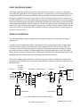
VIDEO PROCESSOR BOARD
This chapter describes the IR video processor for Generation II systems. It serves two functions processing and digitizing the video output from the IR focal plane array (FPA) and supplying DC bias
voltages to the FPA. It contains two identical video processing circuits that simultaneously process
and digitize signals from two FPA video outputs. Two 16-bit analog-to-digital (A/D) converters are
provided on the board, each with a total sample and conversion time of one microsecond. Their digital
outputs are multiplexed on the backplane on dedicated A/D data pins where they are read by the timing
board and then transmitted to the host computer. The DC bias supply section of the board provides six
separate low noise, digitally programmable voltages with a variety of voltage ranges suitable for direct
connection to FPAs, as well as two offset voltages for the two video processors. A block diagram of
the board is shown in Fig. 1.
THEORY OF OPERATION
The FPA output signal, usually amplified by an external preamplifier, is connected to the input
connector P1
A simple x2 gain inverting stage follows the integrator and accepts an output offset voltage from a
DAC that allows a voltage to be subtracted from the signal before the A/D conversion. The A/D
converter is a fast 16-bit part that samples its input for 300 nanoseconds before its start A/D signal
goes high and requires another 700 nanoseconds before its digital output data is valid. The digital
output data are written to a latch when the XFER signal is clocked high, and then transmitted over the
backplane when the timing board asserts the appropriate A/D selection lines.
Some of the analog switches need to be switched every pixel, and are controlled by a simple latch
operating from the WRSS (write switch state) signal from the timing board that can be updated every
40 nanoseconds.
CCD OS
AC or DC
Coupled
Preamp
Post Amp
Gain Select
Polarity Select
Integrator
16-bit
3.9 nf
1k
Source
Follower
Resistor
R1, R51
1 µsec
Integrate
x4 gain
1 nf
x2 gain
A/D
3.9 nf
DC Restore
Reset
Integrator
x1 to x9.5 gain
12-bit
Output Offset
Input Offset
12-bit
DAC
DAC
Fig. 1: Block diagram of the CCD video processor
IR Video Processor, pg. #1
Updated June 8, 1999
TABLE 1 - Fast timing analog switch definition
Function
Schematic name
Start A/D #A
AD-A
Transfer counts #B
XFER-A
Not used
Not used
Start A/D #B
AD-B
Transfer counts #B
XFER-B
Not used
Timing
SS0
SS1
SS2
SS3
SS4
SS5
SS6-11
Description
Low to high transition starts conversion
Low to high transition latches A/D counts
Low to high transition starts conversion
Low to high transition latches A/D counts
The 12-bit DAC circuits for the DC bias supplies receive their digital data words over serial lines from
the PAL U8 that converts 24-bit words from the timing board’s synchronous serial interface (SSI) to
16-bit serial words routed to the two DACs on the video board. The polarity of the DAC outputs can
be selected with jumpers JP15-16 (for DAC U21 that generates the first four voltages listed in the table
below) and JP17 and 19 ( for the DAC U24 that generates the remaining four voltages). For PICNIC
and HAWAII arrays positive voltages are required so the DACs are both set for unipolar positive
outputs. The first two outputs are routed to an offset control that shifts the A/D counts around. The
remaining six outputs are passed through DG405 switches whose function is to be open whenever
there is reason to suspect that the voltages are not set to their proper values or the power supply to the
controller has failed. The control line TIM-D-ENCK controlled by the timing board is set high to close
the switches and allow the DC bias voltages to propagate to the output connector. RC filters then
decouple any remaining noise on the lines. The table of available voltages follows, where names are
assigned to some of the DC bias signals used to operate PICNIC or HAWAII FPA with two video
processor boards. A wiring list is available that maps the pins on the controller boards to the sensor
pins, along with DSP timing board readout code for these two arrays.
TABLE 2 - DC bias voltages definitions for positive unipolar operation
DB15 pin #
None
None
1
2
3
4
5
6
9
10
11-15
Function
OFFSET-A
OFFSET-B
VOFFSET
VRESET
VD
ICLT
VDD
NOT USED
Voltage range
0 to +5
0 to +5
0 to +5
0 to +5
0 to +5
0 to +5
DAC address Default
Voltage
$nC0xxx
$nC4xxx
$nC8xxx
+3.70
$nCCxxx
+0.50
$nD0xxx
+5.00
$nD4xxx
+3.70
$nD8xxx
+4.00
$nDCxxx
IR Video Processor, pg. #2
Description
A/D offset, ch. A
A/D offset, ch. B
Preamp offset
Reset
Analog power
Current control
Digital power
not used
+15 volts power
-15 volts power
Ground
Updated June 8, 1999
BOARD LAYOUT AND POWER REGULATION
An engineering drawing showing the layout of the parts are available in postscript format as filename
vpIRparts4C.lpsf. A schematic of the board is available in postscript format with a filename of
vpIRsch4C.lpsf. Both files are sized to be printed on 11x17 inch paper, though the user can adjust
scaling parameters at the beginning of the file to print on other sized paper.
The layout of the principal components of the video processor board is shown in Fig.2.
The DC bias voltages are output on the large 15-pin DB connector at the lower left of the board
following the pinout of Table 2. Power supply test points are provided below the A/D converters near
the center of the board. These monitor the analog power supply voltages that power the op amps and
A/D converters on the board, as derived from the on-board regulators. The user can conveniently
probe these test points to ensure that the voltages are within range. The tolerances required by the A/D
converter to operate within specifications are pretty tight: +/- 0.50 volts on the two fifteen volt supplies
and +/- 0.25 volts on the two five volt supplies. Trim resistors R75 and R76 are located in the regulator
circuit for adjusting these voltages to be within range, which is done for each board after the
components are installed. These voltages should be within +/- 0.15 of their nominal values. There is
an additional test point in the lower right hand corner of the board labelled VCC that connects to the
digital five volts supply, which is not regulated on this or any other controller board. The theoretical
tolerance of the digital supply is +/- 0.25 volts.
Four on-board regulators provide the analog voltages for the board. They are all low overhead regulators to permit low power dissipation on the board, but since the A/D converters have tight tolerances
on their supply lines users supplying their own system power should pay careful attention that the
overhead requirements of the regulator and that the circuit is trimmed to meet the voltage specification
of the A/D converters. The voltages supplied to the video board are normally set at +/- 16.5 volts to
allow adequate overhead. The A/D converters require +/- 5.0 volt power, which is derived either from
the +/- 16.5 volts supply.
Skip - The section below is all wrong !
BOARD JUMPERING
Fig. 3 shows an enlargement of the jumpers that need configuring on the board. The parts layout of the
preamp and input offset circuitry is shown on the left where the top channel jumpers for channel A are
shown configuring the preamp for AC coupling. The lower channel B is shown configured for DC
coupled operation. For ease of setup the default jumpers are put in the AC coupled mode.
The ground jumper JP9 that is used to connect the analog and digital grounds planes on the board is
shown in the figure. Lower readout noise has been found in prototype systems with the jumper
installed, and on many boards this jumper is not installed but rather a wire is soldered in place of R92
right next to it. The user may cut the wire in R92 at will to break the connection between digital and
analog ground planes if desired, and install a jumper header in JP9 to easily switch back and forth to
determine the minimum noise configuration. The jumpers JP20 and JP21 select between obtaining the
IR Video Processor, pg. #3
Updated June 8, 1999
power for the +/- 5 volts regulated supplies from either +/-16.5 volts (jumpers on bottom) or from
+/-6.5 volts (jumpers on top).
The board addressing jumpers JP1 to JP8 determine the addresses of the DACs, A/D converters and
timing switches. The four jumpers on the left side JP1 to JP4 in the schematic, labelled DAC-A/D 0 to
3 on the silk screen layer on the board, determine the board address for reading the contents of the two
A/D converters and for setting the value of the DACs. An installed jumper will be read as a zero, and
an uninstalled jumper will be read as a one. The four jumpers set the address of the four most
significant bits of the five addressing bits allowed in a system, with the least significant bit selecting
the A (bit D0 = 0) or B (bit D0 = 1) channel. A maximum of sixteen video processing boards may be
installed in a system. As discussed in the timing board user’s manual, the A/D counts may be read
either by the DSP reading from the RDAD memory mapped locations Y:$FFA0 to $FFBF. Alternately, the SXMIT command may be used to read a several A/Ds, possibly on several different boards, and
transmit them as a series to the host computer, bypassing the timing board DSP entirely, as described
in the timing board user’s manual. The example below describes several different jumper settings and
the DSP instructions required to read from a single video processor board.
And several examples for more than one A/D board:
ON ON ON ON
OFF ON ON ON
Y:$FFA0 to FFA3
$00F060
Read four A/Ds, boards 0 and 1
The jumper JP1 to JP4 also select the board address when the timing board writes to the DACs. The
DAC and A/D board addresses are always the same, and there is one set of DACs per video board
addressed from one jumper setting, allowing for a maximum of 16 video processor boards per system.
The most significant bits D20 to D24 of the serial word written out over the backplane pins
TIM-A-STD match the jumpers JP1 to JP4 to select the video processor board to be written to, and the
bits D14-D17 select which of the four DACs on a board and which of each of its internal four DAC
addresses is addressed, following Table 3 above. Bits D18 and D19 must be high to select a video
processing board, while if they are not both high a clock driver DAC is addressed.
The four jumpers on the right side JP5 to JP8 in the schematic, labelled switch 0 to 3 on the silk screen
layer, determine the address that the fast timing analog switches will respond to. Generally all the
video boards in a system are have the same timing jumpers and have the same timing, though 16
timing addresses are provided. The supplied DSP code always sets the video board timing address to
zero, and all four jumpers are installed.
IR Video Processor, pg. #4
Updated June 8, 1999