1
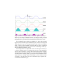
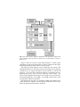
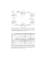
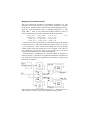
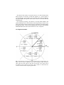
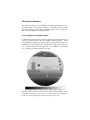
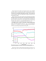
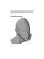
DEVELOPMENT OF A REAL-TIME FULL-FIELD
RANGE IMAGING SYSTEM
A. P. P. Jongenelen1, A. D. Payne2, D. A. Carnegie1, A. A. Dorrington2,
and M. J. Cree2
1
School of Engineering and Computer Science,
Victoria University of Wellington, Wellington, New Zealand
[email protected]
2
Department of Engineering,
University of Waikato, Hamilton, New Zealand
ABSTRACT
This article describes the development of a full-field range imaging system
employing a high frequency amplitude modulated light source and image
sensor. Depth images are produced at video frame rates in which each
pixel in the image represents distance from the sensor to objects in the
scene.
The various hardware subsystems are described as are the details about the
firmware and software implementation for processing the images in realtime. The system is flexible in that precision can be traded off for decreased acquisition time. Results are reported to illustrate this versatility
for both high-speed (reduced precision) and high-precision operating
modes.
1 INTRODUCTION
Range Imaging is a field of electronics where a digital image of a scene is
acquired, and every pixel in that digital representation of the scene records
both the intensity and distance from the imaging system to the object. The
technique described here achieves this by actively illuminating the scene
and measuring the time-of-flight (TOF) for light to reflect back to an image sensor [1-5]. Alternative techniques for forming range or depth data
include stereo vision, active triangulation, patterned light, point scanners
and pulsed TOF [6-8].
Applications of range imaging can be found in mobile robotics, machine
vision, 3D modelling, facial recognition and security systems.
This article describes the development of a full-field range imaging system assembled from off-the-shelf components. The system employs a
modulated light source and shutter set up in a heterodyning configuration
[9] as described in Section 2. Sections 3 and 4 introduce the various hardware components of the system and the software and firmware used to
process the image sequence in real-time and provide control by the user
[10]. A summary of the system is presented in Section 5, illustrating experimental results of captures taken both at high-speed (reduced precision)
for a dynamic scene and also with high-precision in a static scene.
2 TIME-OF-FLIGHT RANGE IMAGING THEORY
The full-field range imaging technique described here utilises an Amplitude Modulated Continuous Wave (AMCW) light source and image sensor
to indirectly measure the time for light to travel to and from the target
scene. In this section we describe two techniques, homodyne modulation
and heterodyne modulation, that we employ for indirect acquisition of
time-of-flight. In both cases the target scene is illuminated by an AMCW
light source with frequency, fM, typically between 10 and 100 MHz.
2.1 Homodyne Modulation
When illuminated by the AMCW light source, objects in the scene reflect
the light back to an image sensor that is amplitude modulated at the same
frequency, fM as the light source. Due to the time taken for the light to
travel to and from the scene a phase delay, , is evident in the modulation
envelope of the received signal.
Fig. 1. Demonstration of pixel intensity as a function of phase delay for light returned from two objects at different distances. The reflected signals are mixed
with a copy of the original modulation waveform producing pixel1 and pixel2. The
total shaded area is proportional to the returned intensity of the pixels, I1 and I2.
The modulated sensor effectively multiplies (or mixes) the returned
light waveform with the original modulation signal. This is then integrated
within the pixel to give an averaged intensity value relative to the phase
offset. Figure 1 shows example waveforms with two objects at different
distances, giving phase shifts θ1 and θ2 for the returned light which produce two different intensities I1 and I2.
From a single frame it is impossible to know if reduced pixel intensity is
a result of the phase offset of a distant object or due to other parameters
such as object reflectance or simply the returned light intensity dropping
with distance by the relationship I/d2. To resolve this ambiguity, N frames
are taken with an artificial phase step introduced in the modulated sensor
signal relative to the light signal incrementing by 2π/N radians between
each frame. The phase delay can now be calculated using a single bin Discrete Fourier Transform as [11]
⎛
⎛ 2πi ⎞ ⎞
⎜ ∑ I cos⎜
⎟⎟
⎝ N ⎠⎟
θ = arctan⎜
⎜
⎛ 2πi ⎞ ⎟
⎜ ∑ I sin ⎜ N ⎟ ⎟
⎝
⎠⎠
⎝
(2.2.)
i
i
where Ii is the pixel intensity for the ith sample. Typically N = 4 as this
simplifies the calculation to [12]
⎛I −I
⎝I −I
θ = arctan⎜⎜
0
2
1
3
⎞
⎟⎟
⎠
(2.3.)
removing the need for storing or calculating the sine and cosine values. It
is also simpler for the electronics to introduce the artificial phase shifts
π/2, π and 3π/2 radians by deriving the signal from a master clock operating at twice the modulation frequency.
From the phase shift, , the distance can then be calculated as
d=
cθ
4πf
(2.4.)
M
where c is the speed of light and fM is the modulation frequency.
2.2 Heterodyne Modulation
Heterodyne modulation differs from homodyne modulation in that the illumination and image sensor are modulated at slightly different frequencies. The illumination is modulated at the base frequency, fM, and the sensor is modulated at fM + fB where the beat frequency, fB is lower than the
sampling rate of the system. The sampling rate, fS, is ideally an integer
multiple of fB as calculated by Equation 2.5.
f =
B
f
N
S
(2.5.)
The effective result is a continuous phase shift rather than the discrete
phase steps between samples of the homodyne method. The phase shift
during the sensor integration period reduces the signal amplitude, in particular attenuating higher frequency harmonic components which can contaminate the phase measurement, producing nonlinear range measure-
ments. Through careful selection of N and the length of the integration
time, the heterodyne method minimizes the effects of harmonics better
than is normally possible with a homodyne system. This enhances measurement accuracy [13].
Another advantage is the ability of the system to easily alter the value of
N from three to several hundred simply by changing the beat frequency.
This allows the user to select between high-speed, reduced-precision
measurements with few frames (N small) or high-precision measurements
with many frames (N large).
3 HARDWARE COMPONENTS
A working prototype of a heterodyne ranging system has been constructed
at the University of Waikato (Hamilton, New Zealand) from off-the-shelf
components. This consists of an illumination subsystem, industrial digital
video camera, image intensifier unit to provide the high-speed sensor
modulation, high-frequency signal generation and support electronics for
real-time range processing and control. Fig. 2 shows an overview of the
hardware configuration.
Fig. 2. Heterodyne Ranger system hardware configuration with three modulation
outputs identified as (1) fM, (2) fM + fB, (3a) mfS and (3b) fS.
3.1 Camera
A Dalsa Pantera TF 1M60 [14] digital camera is used to record the image
sequence. It has a 12-bit ADC and a resolution of up to 1024 × 1024 pixels at a frame rate of up to 60 Hz. For this application the camera is set to
operate in 8 × 8 binning mode improving the per pixel signal to noise ratio
and increasing the maximum frame rate to 220 Hz. The reduced 128 × 128
resolution also eases the real-time processing memory requirements. The
video data stream is provided from the camera via the industry standard
CameraLink interface [15].
3.2 Image Intensifier
A Photek 25 mm single microchannel plate (MCP) image intensifier is
used to provide high-speed gain modulation of the received light. Gated
image intensifier applications typically pulse the photocathode voltage
with 250 Vp-p at low repetition rates to provide good contrast between on
and off shutter states, but this is not feasible for continuous modulation at
frequencies up to 100 MHz. Instead the photocathode is modulated with a
50 Vp-p amplitude signal that can be switched at the desired high frequencies, but at the expense of reduced gain and reduced image resolution [16].
In this particular application, the reduction in imaging resolution does not
impede system performance because the camera is also operated in a reduced resolution mode (8 × 8 binning mode).
3.3 Laser Illumination
Illumination is provided by a bank of four Mitsubishi ML120G21 658 nm
wavelength laser diodes. These diodes are fibre-optically coupled to an illumination mounting ring surrounding the lens of the image intensifier.
This enables the light source to be treated as having originated co-axially
from the same axis as the camera lens and reduces the effect of shadowing.
The fibre-optics also act as a mode scrambler providing a circular illumination pattern, with divergence controlled by small lenses mounted at the
end of each fibre. Maximum optical output power per diode is 80 mW
which is dispersed to illuminate the whole scene.
3.4 Modulation signal generation
The heterodyne ranging technique requires two high frequency signals
with a very stable small difference in frequency. In order to calculate absolute range values, an additional third signal is required to synchronise the
camera with the beat signal so that samples are taken at known phase offsets.
A circuit board containing three Analog Devices AD9952 Direct Digital
Synthesizer (DDS) chips is used to meet these requirements [17]. The
board uses a 20 MHz temperature-controlled oscillator which each DDS
IC multiplies internally to generate a 400 MHz system clock. The DDS
ICs also have the ability to synchronise their 400 MHz system clocks to
remove any phase offset between the outputs.
The output signals are sinusoidal with each frequency programmed by a
32-bit Frequency Tuning Word, FTW, via the SPI interface of an Atmel
89LS8252 microcontroller. The output frequency, f, is calculated as
f =
f FTW
2
SYS
(3.1.)
32
where fSYS is the 400 MHz DDS System clock frequency [18]. This implies a frequency resolution of 0.093 Hz corresponding to the minimal increment of one in the FTW.
The three signals generated by the DDS board are used for:
1) the laser diode illumination, fM,
2) the modulation of the image intensifier, fM + fB and
3) the camera frame trigger multiplied by a constant, mfS.
The DDS outputs derived from the same master clock ensures appropriate frequency stability between the beat signal, fB, and the camera trigger
mfS.
A Xilinx Spartan 2 Field Programmable Gate Array (FPGA) receives
the sinusoidal mfS signal, and using a digital counter divides the signal
down to produce a CMOS signal of fS used to trigger the camera. This
produces less jitter than that produced by the alternative of passing the less
than 200 Hz sinusoidal signal directly to a comparator to effect a sinusoidal to digital conversion.
3.5 Control Hardware
The Spartan 2 board controls the analogue gain of the image intensifier
and the laser diodes using a pair of Digital to Analogue Converter ICs.
The gain control of the laser diodes is used to ensure that they are slowly
ramped on over a period of several minutes to protect them from overpower damage before they reach the stable operating temperature (operating in constant current mode). Controlling the gain of the image intensifier
ensures the full dynamic range of the camera sensor is utilised while preventing pixel saturation.
Top level control of the system is provided through an Altera Stratix II
FPGA resident on an Altera Nios II Development Kit connected via a
JTAG connection to a PC. Control instructions are processed by a Nios II
soft processor core and written to either special function registers within
the Stratix II FPGA or passed on via RS232 to the microcontroller of the
DDS board. The Spartan 2 board is controlled through an 8-bit port of the
DDS board microcontroller.
3.6 Processing Hardware
In addition to providing top level control of the various hardware components of the system, the Stratix II FPGA is used to process the image sequence and calculate the range data using Equation 2.2.
Frames are directly transferred from the Dalsa camera over the CameraLink interface to the FPGA. A daughter board utilising a National
Semiconductor DS90CR286 ChannelLink Receiver IC is used to convert
from the serial LVDS CameraLink format to a parallel CMOS format more
acceptable for the general purpose I/O pins of the FPGA.
The camera has two data taps, each streaming pixel information at a rate
of 40 MHz. The images from the camera are processed internally within
the FPGA and temporarily stored in on-chip block RAM ready to be presented to the user.
3.7 User Interfaces
The system is controlled through the Altera Nios II terminal program,
which communicates with the Nios II processor through a JTAG interface.
This is used to set system parameters including frame rate, modulation frequency, beat frequency, number of frames per beat, image intensifier gain,
laser diode gain and various other special function registers.
For real-time range data display, a daughter board with a Texas Instruments THS8134 Triple 8-bit DAC IC is used to drive a standard VGA
monitor. For longer term storage and higher level processing the range
data are transferred to a PC using a SMSC LAN91C11 Ethernet
MAC/PHY chip resident on the Nios II Development Kit. The embedded
Nios II software handles the fetching of the temporarily stored range data
from the block RAM and sends it out through a TCP connection to a host
PC.
4 SOFTWARE AND FIRMWARE COMPONENTS
There are three distinct sets of software involved in operating the system,
namely:
1) Firmware for the real-time calculation of range data on the Stratix II
FPGA,
2) Software on the Nios II processor and
3) Host software on the PC.
4.1 Range Processing Firmware
The data stream coming from the camera consists of two pixel channels at
40 MHz each. It is very difficult to calculate the phase shift of each pixel
using Equation 2.2 in real-time with current sequential processors,
whereas the configurable hardware of the FPGA is ideally suited to this
task as it can perform a large number of basic operations in parallel at the
same clock rate as the incoming pixels.
Fig. 3. Top level overview of FPGA configuration. The data path of captured and
processed image frames are shown as white arrows. Control signals are shown as
black arrows.
Figure 3 shows an overview of the FPGA firmware. Control signals
originating from the user-operated PC are shown in black and the image
data path originating from the camera is shown in white.
The range processing firmware can be divided into four sections: The
CameraLink interface to the Dalsa Camera, the multiply and accumulate
calculation, the arc tangent calculation, and the interface to the Nios II
processor. All of the range calculation firmware is instantiated twice to
independently process each of the two output taps of the camera. The
process is fully pipelined with a latency of 24 clock cycles, and a theoretical maximum frequency of 144 MHz. A 125 MHz system clock is used
for all elements internal to the FPGA.
The firmware for this project is designed in VHDL and simulated using
Aldec’s Riviera Pro software. Altera’s Quartus II software is used to synthesise the design and download it to the board.
The CameraLink Interface
The interface to the Dalsa camera consists of 27 parallel inputs with a
40 MHz clock input for providing the pixel data, one output for the frame
trigger of the camera, and one line in each direction for UART serial
communication [15].
The frame trigger is provided directly from the Spartan 2 board and
simply passes through the interface to the camera. The serial communication lines are handled by the Nios II processor.
All of the 40 MHz data lines are sampled at the 125 MHz FPGA system
clock. The lval and fval control inputs are used to specify when a valid
line and frame of data are being received respectively. These are monitored by a state machine as shown in Figure 4 to give feedback to the system when a new frame is complete.
The state machine first ensures that it is aware of which part of the
transfer sequence is currently underway, either during integration while the
frame trigger is high or during readout while fval is high. While the frame
and line valid signals are both high, valid pixel data are sampled on the falling edge of the 40 MHz clock. Once the frame and line valid signals are
both low the readout is complete and a counter is started to introduce a delay before the frame increment signal is pulsed high. This allows the processing electronics time to complete before various registers and look-uptables are updated for the next frame. Figure 5 shows the timing of the
signals within the CameraLink interface.
Fig. 4. CameraLink finite state machine for tracking incoming frames. Data readout is initiated by a falling edge of trigger and is read from the camera during the
FVAL_HIGH state. A high pulse of frame_inc is generated a short time after readout is complete to prepare the system for the next frame.
Fig. 5. Timing of the signals internal to the CameraLink interface. Readout from
the camera is initiated by a falling edge of the trigger signal. Data is transferred
from the camera synchronous to a 40 MHz clock, and is sampled within the FPGA
using a 125 MHz clock. When fval and lval are high, the falling edge of the 40
MHz clock generates a high pulse of pixel_valid.
Multiply and Accumulate Firmware
This section details the calculation of summations in Equation 2.2. The
equation is first broken down into a series of basic operations to calculate
the numerator and denominator (termed as the real and imaginary parts respectively) using intermediate values as labelled in Equation 4.1. The
frame index, i, refers to the current frame number between 0 and N-1
which is incremented with each iteration through the state machine.
real_new =
imag_new =
real_acc
imag_acc
raw_pixel . cos_lut(i)
raw_pixel . sin_lut(i)
= real_new + real_old
= imag_new + imag_old
(4.1.)
The sine and cosine operations are pre-calculated based on the number
of frames per beat, N, and stored in the look-up-tables (LUTs) sin_lut and
cos_lut respectively. These values can be changed by the user through
control registers when the desired value of N is changed. The values for
real_old and imag_old are the values of real_acc and imag_acc from the
previous frame which have been stored in block RAM.
Each operation is implemented as a dedicated block of hardware as
shown by Figure 6. Operations are pipelined such that the calculation for
any newly received pixel can begin before the calculation of the previous
pixel is fully completed.
Fig. 6. Firmware block diagram implementing equation 4.1. Each operation has a
dedicated block of hardware and the whole calculation is fully pipelined.
Not shown is the circuitry to reset the value of i to 0 after N frames have
been processed. At the start of each beat sequence (i = 0) the values of
real_old and imag_old are taken as 0 to clear the value of the accumulator.
The block RAM is dual ported, which allows values to be written and read
simultaneously.
For real-time processing, the amount of on-chip block RAM is the
greatest limiting factor in the resolution of the range images, because every
pixel of the image requires enough storage for both the real and imaginary
accumulated values. In the current implementation using an Altera Stratix
II EP2S60 FPGA this restricts the resolution to 128 × 128 pixels.
Arc Tangent Calculation
Fig. 7. Calculation of arc tangent using one eighth of the LUT requirements. Using the sign and relative magnitude of the real and imaginary inputs determines
which region the result will be in. The index into the LUT is the scaled result of
the smallest of the two divided by the largest. This is added to or subtracted from a
constant to find the final arc tangent approximation.
The arc tangent is approximated using a look-up-table (LUT). Figure 7
shows how the symmetric nature of the arc tangent function is utilised to
reduce the RAM requirements of the LUT to one eighth of the full cycle.
The sector, out of the eight possible sectors, of the final result is determined by the sign and magnitude of the real and imaginary components.
The division is calculated and used to index the LUT, and the intermediate
result is added to or subtracted from a constant to give the final result.
The advantage of calculating the arc tangent in this way is that the result
of the division is always a positive number between 0 and 1. This scales
easily as an index into the look-up-table. With a 16-bit by 1024 point
LUT, the arc tangent can be approximated to better than 0.8 milliradians.
Interface to Nios II processor
The output frame from the arc tangent function is stored in a portion of triple port block RAM. The three ports are designated as one write-only port
for the result of the arc tangent calculator and two read-only ports: one for
the VGA display driver and the other for the Nios II processor.
The Nios II processor addresses 32k memory locations in the hardware.
The lower 16k reference the output RAM, and the upper 16k reference
special function control registers. These registers control everything
within the Stratix II FPGA such as sine and cosine LUT values, frames per
beat and a synchronous reset. Two control registers are set up in relation
to the transfer of data to the processor:
• OR_RDY : a 1-bit read-only register which is set high by hardware
when a processed frame is available in the output RAM.
• OR_ACK : a 1-bit write-only register which is used to signal to the
hardware that reading of the output RAM is complete.
While the OR_RDY bit is high, writing into the output RAM is disabled.
This ensures that a frame being transferred out is not inadvertently
overwritten.
4.2 Nios II Software
The Nios II processor is a reconfigurable microprocessor core provided by
Altera. The features of the processor can be selected using the SOPC
builder available with the Quartus II software.
For this application, a processor has been designed with the following features:
• Nios II Processor with 4 kB instruction cache
• 32 MB DDR SDRAM
• Three serial UART interfaces for
o DDS control
o Dalsa camera control
o PC user interface
• LAN91C111 ethernet MAC/PHY
• 16 × 2 character LCD display
• 32-bit parallel interface to on-chip ranger hardware
The Nios II processor is programmed in C using the Nios II IDE software. The main tasks performed by the processor are to:
1) Parse text commands from the user and either
a) read or write on-chip control registers
b) forward the message on to the DDS board microcontroller
c) forward the message on to the Dalsa camera
2) Respond to the OR_RDY signal generated by the processing
hardware, and
3) Handle the TCP connection for transferring frames to the PC.
A multi-threaded program is used for these tasks with the TCP packet
handler having top priority. While the multi-threaded environment does
add extra complexity and overhead to the code, an Altera example design
with ethernet and TCP/IP configuration functionality was simply modified
to include the additional required tasks.
4.3 PC Software
Software on the PC is programmed in C# using Microsoft Visual Studio.
A basic terminal program establishes a TCP connection with the Nios II
processor of the Stratix II FPGA, listening for incoming packets and writing them to a binary file.
The Nios II IDE software also includes a terminal for communicating
with the Nios II processor through JTAG. This interface is used for sending text commands to the Nios II processor for setting various control parameters.
5 Results and Summary
The following results give an indication of ranging performance for two
operating modes of the system: a capture of a dynamic scene for highspeed range images at the expense of depth precision, and a capture of a
static scene for high precision measurements.
5.1 Test Capture of a Dynamic Scene
To demonstrate the operation of the range imaging system with video-rate
output a scene has been set up with a number of moving objects. These
are a pendulum swinging in a circular motion, a bear figurine rotating on a
turntable and a roll of paper towels rolling down a ramp towards the camera. System parameters for this capture are fM = 40 MHz, fS = 125 Hz and
N = 5, resulting in 25 range images per second.
Fig. 8. First range image frame of dynamic test capture with identified test pixels:
1) cardboard background, 2) far wall, 3) to 5) pixels tracking the rolling paper
towels. Grey scale pixel intensity represents range from 0 to 3.75 m.
Figure 8 shows the first frame of the sequence with a group of labelled
test pixels. These are locations in the capture showing 1) the area above
the bear imaging a cardboard background, 2) a region of the far wall of the
room and 3) to 5) the path of the rolling paper towels. The rotating bear
and the pendulum, which is the dark spot to the right of the bear are not
analysed in this capture
Figure 9 shows a plot of the test pixels as their measured range changes
throughout the 40 range image capture. As expected for stationary objects,
the range at pixels 1 and 2 does not change throughout the capture and
give an indication of the precision of the system in this operating mode.
Test pixel 1 has a mean of 3.11 m and standard deviation of 4.0 cm and
test pixel 2 has a mean of 1.27 m and standard deviation of 3.6 cm.
Although test pixel 2 represents the far wall, it is measured to be a distance similar to pixel 5. This is a consequence of phase wrapping where
objects beyond the unambiguous range of c / 2fM = 3.75 m are measured
incorrectly. It is possible to correct for this ambiguity [9] but this functionality is not currently incorporated into this system.
Fig. 9. Measured range of test pixels throughout 40 range image sequence:
1) cardboard background, 2) far wall, 3) to 5) points on the rolling paper towels.
The plot also shows an interconnecting slope between test pixels 3 to 5
where the paper towels roll towards the camera through these pixels. For
example, test pixel 4 is initially returning the range of a location on the
ramp at approximately 2.4 m. Between frames 17 and 24 the paper towels
roll towards the camera through the location imaged by this pixel evident
as a decreasing range measurement. After the paper towels have gone past
the location of pixel 4 the value returns to the initial range of 2.4 m.
5.2 Test Capture of a Static Scene
Fig. 10. High precision three-dimensional reconstruction of a person’s face.
Figure 10 shows a three-dimensional mesh plot reconstructed from range
image data. This capture was taken over 10 seconds with fM = 80 MHz,
fS = 29 and N = 29 Hz. The combination of large integration time, the high
number of frames per beat and averaging over 10 beat cycles results in a
range image with a standard deviation of less than 1 mm.
5.3 Summary
This article has described the construction of a heterodyne range imaging
system with video-rate depth image output. The system has the following
parameters:
• x-y resolution of 128 × 128 pixels
• variable output frame rate with real-time display up to 60 Hz
• variable frames per beat, N
• variable modulation frequency, fM, up to 80 MHz
• data capture using a common ethernet interface
• system parameters adjustable through a command line interface
With these easily adjustable system parameters it is possible to configure the system to meet the needs of a wide variety of applications from 3D
modeling to mobile robotics.
References
[1]
[2]
[3]
[4]
[5]
[6]
[7]
Christie, S., et al.: Design and development of a multi-detecting twodimensional ranging sensor. Measurement Science and Technology 6,
1301–1308 (1995)
Kawahito, S., et al.: A CMOS Time-of-Flight range image sensor with
Gates-on-Field-Oxide structure. IEEE Sensors 7, 1578–1586 (2007)
Lange, R., Seitz, P.: Seeing distances – a fast time-of-flight 3D camera.
Sensor Review 20, 212–217 (2000)
Gulden, P., et al.: Novel opportunities for optical level gauging and 3-D
imaging with the Photoelectronic Mixing Device. IEEE Transactions on Instrumentation and Measurement 51, 679–684 (2002)
Buttgen, B., et al.: High-speed and high-sensitive demodulation pixel for
3D-imaging. In: Proc. SPIE – Three-dimensional image capture and applications, vol. 7 (2006)
Blais, F.: Review of 20 years of range sensor development. Journal of Electronic Imaging 13, 231–243 (2004)
Besl, P.J.: Active, Optical range imaging sensors. Machine Vision and Applications 1, 127–152 (1988)
[8]
[9]
[10]
[11]
[12]
[13]
[14]
[15]
[16]
[17]
[18]
[19]
Sato, K.: Range imaging based on moving pattern light and spatio-temporal
matched filter. In: International Conference on Image Processing, vol. 1,
pp. 33–36 (1996)
Dorrington, A.A., et al.: Achieving sub-millimetre precision with a solidstate fullfield heterodyning range imaging camera. Measurement Science
and Technology 18, 2809–2816 (2007)
Jongenelen, A.P.P., et al.: Heterodyne range imaging in real-time. In: Proc.
International Conference on Sensing Technology, Tainan, vol. 3, pp. 57–62
(2008)
O’Shea, P.: Phase Measurement. In: Webster, J.G. (ed.) Electrical Measurement, Signal Processing and Displays, pp. 28–41. CRC Press, Boca
Raton (2003)
Lange, R., Seitz, P.: Solid-state time-of-flight range camera. IEEE Journal
of Quantum Electronics 37, 390–397 (2001)
Dorrington, A.A., et al.: Video-rate or high-precision: a flexible range imaging camera. In: Proc. SPIE Image Processing: Machine Vision Applications, vol. 6813 (2008)
DALSA, Pantera TF 1M60 and 1M30 User’s Manual and Reference
(2004), http://www.dalsa.com
PULNiX America Inc., Specifications of the Camera Link Interface Standard
for
Digital
Cameras
and
Frame
Grabbers
(2000),
http://www.imagelabs.com
Payne, A.D., et al.: Image intensifier characterisation. In: Proc. Image and
Vision Computing, New Zealand, pp. 487–492 (2006)
Payne, A.D., et al.: A synchronized Direct Digital Synthesiser. In: Interntional Conference on Sensing Technology, Palmerston North, pp. 174–179
(2005)
Analog Devices, 400 MSPS 14-Bit, 1.8 V CMOS Direct Digital Synthsizer
AD9952 Datasheet (2009), http://www.analog.com
Altera Corporation, Stratix II Device Handbook, vol. 1 (2007),
http://www.altera.com