1
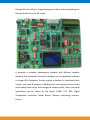
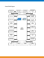
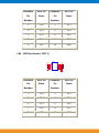
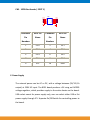
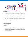
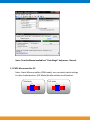
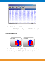
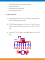
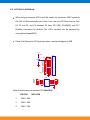
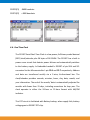
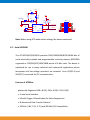
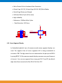
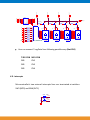
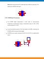
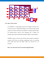
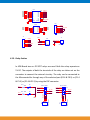
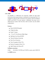
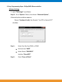
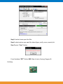
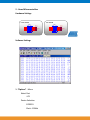
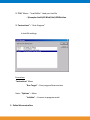
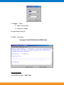
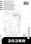
MICRO CONTROLLER BOARDS 8051 Advanced Development kit Contents 1. - Introduction ...................................................................................................... 1 1.1– Packages ................................................................................................ 3 1.2- Technical or Customer Support ................ Error! Bookmark not defined. 1.3 - Board Introduction ................................................................................ 4 2. Connectors and Jumper Details ........................................................................... 8 3. Power Supply .................................................................................................... 11 4. MCU Sockets ..................................................................................................... 12 5. Flash Programming Utility ................................................................................. 12 6. On-board Peripherals ........................................................................................ 15 6.1 - Light Emitting Diodes .......................................................................... 16 6.2 – Digital Inputs Slide Switch................................................................... 17 6.3 - LCD 2x16 In 8-Bit Mode ....................................................................... 18 6.4 - 128X64 Graphic LCD ............................................................................ 19 6.5 - RS-232 Communication ....................................................................... 20 6.6 - Real Time Clock ................................................................................... 21 6.7 – Serial EEPROM .................................................................................... 22 6.8 - Seven Segment Display ....................................................................... 23 6.9 - Interrupts ............................................................................................ 24 6.10 - DS1820 Digital Thermometer ............................................................ 25 6.11 - 4x4 Matrix keypad ............................................................................. 26 6.12 - Motor / Driver Section ...................................................................... 27 6.13 - Relay Section ..................................................................................... 28 6.14 - SPI DAC.............................................................................................. 29 6.15 - RS485 ................................................................................................ 30 6.16 - PS/2 Interface.................................................................................... 32 6.17 – Analog / Digital Convertor (SPI ADC)................................................. 32 6.18 – RF433.92MHz ................................................................................... 33 7. Board Layout ..................................................................................................... 37 8. Easy Programming Steps – Atmel | NXP | Dallas Microcontrollers .................... 38 1. - Introduction Thank you for purchasing the SLICKER-8051 Kit. You will find it useful in developing your 8051 application. SLICKER-8051 Kit, is proposed to smooth the progress of developing and debugging of various designs encompassing of High speed 8-bit MCU from NXP/Dallas/Atmel. The board supports 8051 family devices with various memory and peripheral options. It integrates on board two UARTs, LEDs, Relays, Motor Interface, keypads, an ADC input and GLCD/LCD Display to create a stand-alone versatile test platform. 1.1– Packages SLICKER-8051 Kit (NXP - P89V51RD2 MCU) Serial Port Cable | Parallel Cable for Atmel Printed User Manual 10-PIN FRC cables CD contains Software (Programmers, IDE) o Example Programs User Manual 1.1- Technical or Customer Support E-mail questions to [email protected] Send questions by mail to Pantech Prolabs India Pvt Ltd., #41, Rajeswari Street, Santhosh Nagar, Kandhanchavadi, Chennai – 600 096. Tamilnadu, India Phone : +91-44-64524445/46/47 Fax : +91-44-4260 6350 Website : www.pantechsolutions.net 1.3 - Board Introduction Pantech Solutions’ Embedded Advanced Development module is proposed to smooth the progress of developing and debugging of various designs encompassing 8051 Microcontrollers from Philips / Atmel/ Dallas. The intention of the design is to endorse the engineers to exercise and explore the capabilities of 8051 microcontrollers with many communication protocol ease. The board is compatible with 40-DIP/44-PLCC pin Microcontrollers. The kit is designed so as to facilitate separate On-board ISP Programmer for Atmel microcontrollers and Philips Microcontroller through ISP on serial port. Programming can be done without detaching the Microcontroller from the ZIF socket. It provides a complete development platform with different modules interface that accelerates the task of designers to run application software on target 8051 hardware, thereby paving a platform to benchmark their system, save time & expense of building their own application test board and enabling them to get their designs to market quickly. Many real world applications can be tested on the board. RS485, RTC, DAC, Digital Temperature controllers, Motor drivers, Memory interfacing, counters, timers... General Block Diagram 9V AC/DC Input 5V Regulator USB Connector Power Supply Parallel/Serial ISP Programmer Relay Outputs (2 Nos) RF 433.93MHz Transmitter Receiver 128x64 GLCD 2x16 Char LCD SPI – DAC MCP4921 PS/2 Keyboard I2C EEPROM SPI-ADC Two Channel I2C Real Time Clock AT89SXX DS89C4XX P89V51RD2 Two Relay Outputs 1-Wire Temp Sensor 4x4 Matrix Keypad RS485 4 Nos. Seven Segment Display Stepper Motor Termination 2XRS232 Two Ext Interrupts 8 Nos. Point LEDs 8 Nos. Digital Inputs Specifications Supported Microcontrollers : SOCKET1 (40-DIP) Atmel : AT89S51/52/8252 and AT89Sxx NXP : P89V51Rxx Dallas : DS89C420/430/450 SOCKET2 (44-PLCC) Atmel : AT89S51/52/8252 and AT89Sxx MCUs NXP : P89V51Rxx Dallas : DS89C420/430/450 External Peripheral Modules 128X64 GLCD Interface 2x16 Character LCD with Contrast adjust 4-Nos. of common anode seven segment display 8-Nos. General purpose Point LEDs 8-Nos. of Toggle switches (Digital Inputs) 4x4 Matrix keypad Stepper Motor Driver Output Two Nos. of 5V Relay with termination PS/2 keyboard Interface RF 433.92MHz Transmitter/Receiver Communication Protocols I2C Two Wire Interface (Philips-NXP) SPI (Motorola) 1-wire Technology (Maxim-Dallas) Two Full Duplex UART (EIA) RS485 (EIA) Other Features Analog to Digital Converter Digital to Analog Converter Real Time Clock with Battery Backup Serial EEPROM memory RF 433.92MHz Transmitter/Receiver Digital Temperature sensor RS485 serial communication through long distance(>200m) Two UART for serial port communication through PC. ISP In-System Programming for NXP, Dallas controllers. Parallel programmer for Atmel AT89S5X family controllers. Two pushbuttons for Interrupts study. Easy to mount 40-pin DIP Devices (ZIF socket). Controlling of multifunction through DIP Switch. 2. Connectors and Jumper Details CN3 - 10PIN Box Header ( PORT 0 ) P0.0 P0.2 P0.4 P0.6 VCC CN3 1 3 5 7 9 2 4 6 8 10 P0.1 P0.3 P0.5 P0.7 PORT 0 Connector MCU Pin Connector MCU Pin Pin Name Pin Name Numbers Numbers 1 P0.0 2 P0.1 3 P0.2 4 P0.3 5 P0.4 6 P0.5 7 P0.6 8 P0.7 9 VCC 10 GND CN2 - 10PIN Box Header ( PORT 1 ) P1.0 P1.2 P1.4 P1.6 VCC CN2 1 3 5 7 9 2 4 6 8 10 PORT 1 P1.1 P1.3 P1.5 P1.7 Connector MCU Pin Connector MCU Pin Pin Name Pin Name Numbers Numbers 1 P1.0 2 P1.1 3 P1.2 4 P1.3 5 P1.4 6 P1.5 7 P1.6 8 P1.7 9 VCC 10 GND CN4 - 10PIN Box Header ( PORT 2 ) P2.0 P2.2 P2.4 P2.6 VCC CN4 1 3 5 7 9 2 4 6 8 10 P2.1 P2.3 P2.5 P2.7 PORT 2 Connector MCU Pin Connector MCU Pin Pin Name Pin Name Numbers Numbers 1 P2.0 2 P2.1 3 P2.2 4 P2.3 5 P2.4 6 P2.5 7 P2.6 8 P2.7 9 VCC 10 GND CN5 - 10PIN Box Header ( PORT 3 ) P3.0 P3.2 P3.4 P3.6 VCC CN5 1 3 5 7 9 2 4 6 8 10 P3.1 P3.3 P3.5 P3.7 PORT 3 Connector MCU Pin Connector MCU Pin Pin Name Pin Name Numbers Numbers 1 P3.0 2 P3.1 3 P3.2 4 P3.3 5 P3.4 6 P3.5 7 P3.6 8 P3.7 9 VCC 10 GND 3. Power Supply The external power can be AC or DC, with a voltage between (9V/12V,1A output) at 230V AC input. The 8051 board produces +5V using an LM7805 voltage regulator, which provides supply to the entire device on the board. USB socket meant for power supply only, user can select either USB or Ext power supply through JP1. Separate On/Off Switch for controlling power to the board. JP1 POWER CN1 USB 5 1 2 3 1 D1 1 2 2 - VOUT + 4 1 2 3 4 VCC 3 SW2 2 BRIDGE J1 VIN 78XX/TO GND 1 U1 6 VCC DD+ GND GNDGND 1 2 R1 330E D2 SW KEY -SPST 3 POWER JACK C2 470uf C3 0.1uf 5V1 4. MCU Sockets The 8051-development board is delivered with ATMEL’s 40-pin & 44pin CAN Controller Microcontroller. User can remove this and fit different microcontroller DIP40 packages of an adequate pin out. NOTE : Since all packages have parallel connections, there must not be more than one microcontroller on the board at a time. 5. Flash Programming Utility 1. NXP (Philips) NXP Semiconductors produce a range of Microcontrollers that feature both on-chip Flash memory and the ability to be reprogrammed using In-System Programming technology. D3 LED Note : Detailed Manual available at “Flash Magic” Help menu - Manual. 2. ATMEL Microcontroller ISP Note : Atmel Microcontrollers (PGM mode), user can select switch settings to color shaded position. (EXE Mode) disable switches to off position. PGM Mode EXE Mode SW1 OFF ON SW DIP-4 SW1 P1.7 P1.5 MC_RST P1.6 OFF ON SW DIP-4 P1.7 P1.5 MC_RST P1.6 Note : Detailed Manual available for \8051ADB\Softwares\Programmers\AT89ISP\User Manual.pdf 3. Dallas Microcontroller ISP EXE Mode PGM Mode SW4 1 2 3 4 5 6 7 8 OFF ON SW DIP-8 SW4 16 15 14 13 12 11 10 9 1 2 3 4 5 6 7 8 OFF ON 16 15 14 13 12 11 10 9 SW DIP-8 Note : Dallas Microcontrollers (PGM mode), user can select switch settings to color shaded position.(EXE Mode) disable switches to off position. 6. On-board Peripherals The Development board comes with many interfacing options 8-Nos. of Point LED’s (Digital Outputs) 8-Nos. of Slide switches (Digital Inputs) 2 Lines X 16 Character LCD Display 128X64 GLCD Interface Real Time Clock with battery backup 4 Nos. of Seven-segment display Digital Temperature Sensor 4 X 4 Matrix keypad Relay / Stepper Motor driver circuit SPI Digital to Analog Converter Serial EEPROM memory RS485 serial communication through long distance(>200m) Two UART for serial port communication through PC PS/2 keyboard Interface RF 433.92MHz Transmitter/Receiver SPI Analog / Digital Converter 6.1 - Light Emitting Diodes Light Emitting Diodes (LEDs) are the most commonly used components, usually for displaying pin’s digital states. The 8051 Advanced Development kit has 8 nos., of Point LED, user can interface the point LEDs with any port. User can use P0, P1, P2 and P3 ports. Connector CN7 for LED connector, when High Level goes to the pin LED C 1 glows. 470E D2 D3 D4 D5 D6 D7 CN7 D1 D3 D5 D7 1 3 5 7 9 LED 2 4 6 8 10 D2 D4 D6 D8 LED8 LED7 LED6 LED5 LED4 2 3 4 5 6 7 8 9 LED3 LED2 LED1 3MM LED RED Color D1 R7 D8 6.2 – Digital Inputs Slide Switch This is another simple interface, 8-Nos. of toggle switch, mainly used to give an input to the port lines, and for some control applications also. All the lines are pulled-up, when make to switch ON, it goes to low logic to the i/o pins. 1 VCC 9 8 7 6 5 4 3 2 10K R8 SW15 R10 10k 2 S1 1 SW20 R11 10k 2 S2 1 SW21 R12 10k 2 S3 1 SW26 R13 10k 2 S4 1 SW27 R14 10k 2 S5 1 SW28 R15 10k 2 S6 1 SW29 R16 10k 2 S7 1 SW30 R17 10k 2 S8 1 CN8 S1 S3 S5 S7 1 3 5 7 9 2 4 6 8 10 Digi I/P S2 S4 S6 S8 6.3 - LCD 2x16 In 8-Bit Mode When using a character LCD in an 8-bit mode, the connector CN10 connects the LCD to Microcontroller port lines. User can use LCD Data lines to Port P0, P1 and P2, not P3, because P3 lines P3.5 (RS), P3.6(R/W) and P3.7 (Enable) connected by default. The LCD’s contrast can be adjusted by varying the trimpot(R24). Place 2x16 Character LCD to proper place, mentioned legend in PCB. VCC 1 R24 GND 2 3 10K LCD_P P3.5 P3.6 P3.7 DP1 DP2 DP3 DP4 DP5 DP6 DP7 DP8 LCD_P JP2 1 2 3 4 5 6 7 8 9 10 11 12 13 14 15 16 2x16 LCD CN10 DP1 DP3 DP5 DP7 1 3 5 7 9 2 4 6 8 10 LCD Note: Possible ways to interface LCD (Not CN5). LCD CON 1. CN10 CN2 2. CN10 CN3 3. CN10 CN4 MCU CON DP2 DP4 DP6 DP8 6.4 - 128X64 Graphic LCD When using a Graphic LCD, the connector CN11 connects the LCD to Microcontroller port lines. User can use GLCD Data lines to Port P0, P1 and P2, not P3, because P3 lines P3.3(CS1), P3.4(CS2), P3.5(RS), P3.6(R/W) and P3.7 (Enable) connected by default. The LCD’s contrast can be adjusted by varying the trimpot(R23). Place GLCD to proper place, mentioned in PCB. 3 J2 R23 10K GND GLCD_P 2 1 VCC P3.3 P3.4 P3.5 P3.6 P3.7 GD0 GD1 GD2 GD3 GD4 GD5 GD6 GD7 R32 10E 1 2 3 4 5 6 7 8 9 10 11 12 13 14 15 16 17 18 19 20 GLCD128X64 CN11 GD0 GD2 GD4 GD6 1 3 5 7 9 2 4 6 8 10 GLCD Note: Possible ways to interface LCD (Not CN5). LCD CON 1. CN11 CN2 2. CN11 CN3 3. CN11 CN4 MCU CON GD1 GD3 GD5 GD7 6.5 - RS-232 Communication RS-232 communication enables point-to-point data transfer. It is commonly used in data acquisition applications, for the transfer of data between the microcontroller and a PC. The voltage levels of a microcontroller and PC are not directly compatible with those of RS-232, a level transition buffer such as MAX232 be used. VCC C5 100n RXD1 12 P3.0 9 1 C6 T1OUT T2OUT R1OUT R2OUT R1IN R2IN 14 7 TX1_OUT TX0_OUT 13 8 RX1_IN RX0_IN TX0_OUT RX0_IN COM1 C1+ MAX232/DIP 3 4 C8 5 P3 C1C2+ C2- VV+ 6 C7 10uF 2 C9 10uF TX1_OUT RX1_IN 15 10uF T1IN T2IN GND 10uF VCC 11 10 16 U5 TXD1 P3.1 P2 5 9 4 8 3 7 2 6 1 5 9 4 8 3 7 2 6 1 COM2 : Note : UART0 (PGM) lines connected directly through MCU pins(RXD0, TXD0). For serial communication use UART0(P2). : Note : Make switch positions UART1(P1) for Dallas MCU Only. SW4 P1.2 P1.3 1 2 3 4 5 6 7 8 OFF ON 16 15 14 13 12 11 10 9 RXD1 TXD1 SW DIP-8 Note : Dallas MCU User can’t set 9600 baud rate for both the UART0 and UART1 PORT0(P1) - 9600 baudrate PORT1(P2) – 4800 baudrate 6.6 - Real Time Clock The DS1307 Serial Real-Time Clock is a low power; full binary-coded decimal (BCD) clock/calendar plus 56 bytes of NV SRAM. The DS1307 has a built-in power sense circuit that detects power failures and automatically switches to the battery supply. In Embedded module’s DS1307 of pin SDA and SCL connected to the Microcontroller’s pin P2.6 and P2.7 respectively. Address and data are transferred serially via a 2-wire, bi-directional bus. The clock/calendar provides seconds, minutes, hours, day, date, month, and year information. The end of the month/ date is automatically adjusted for months with fewer than 31 days, including corrections for leap year. The clock operates in either the 24-hour or 12-hour format with AM/PM indicator. This RTC circuit is facilitated with Battery backup, when supply fails; battery voltage goes to DS1307 RTC chip. VCC 1N4148 1N4148 D8 1K R44 D7 D9 3.6V Battery 2 VCC 1 3 X2 1 32.768KHz 2 VBAT X1 X2 R46 4K7 U15 8 1N4148 I2C_RTC BT1 SDA SCLK SQW/OUT SW33 R45 4K7 5 I2C_SDA 6 I2C_SCL 7 P2.6 P2.7 1 2 3 4 5 6 7 8 DS1307 16 15 14 13 12 11 10 9 I2C_SCL I2C_SDA SW DIP-8 Note: Before using RTC make switch settings like above mentioned. 6.7 – Serial EEPROM The AT24C01A/02/04/08/16 provides 1024/2048/4096/8192/16384 bits of serial electrically erasable and programmable read-only memory (EEPROM) organized as 128/256/512/1024/2048 words of 8 bits each. The device is optimized for use in many industrial and commercial applications where low-power and low-voltage operation are essential. Lines CLK(P2.6) and SDA(P2.7) connected for I2C communication. Features of AT24Cxx: Internally Organized 128 x 8 (1K), 256 x 8 (2K), 512 x 8 (4K) • 2-wire Serial Interface • Schmitt Trigger, Filtered Inputs for Noise Suppression • Bi-directional Data Transfer Protocol • 100 kHz (1.8V, 2.5V, 2.7V) and 400 kHz (5V) Compatibility • Write Protect Pin for Hardware Data Protection • 8-byte Page (1K, 2K), 16-byte Page (4K, 8K, 16K) Write Modes • Partial Page Writes are Allowed • Self-timed Write Cycle (10 ms max) • High-reliability – Endurance: 1 Million Write Cycles – Data Retention: 100 Years 8 VCC P2.6 P2.7 I2C_SDA I2C_SCL 5 6 SDA SCL 4 16 15 14 13 12 11 10 9 U13 GNDVCC SW33 1 2 3 4 5 6 7 8 A0 A1 A2 WP 1 2 3 7 AT24CXX I2C_SCL I2C_SDA SW DIP-8 6.8 - Seven Segment Display In Embedded module 4 nos. of common anode seven segment displays are used. The segment lines of seven segments LED is being terminated at connector CN9. The digit select lines are connected to the port pins of 8051 by using BC547. All the common anode displays consume very small amount of current. User can use segment lines at any port P0, P1 and P2, by default digit select lines connected to Port P3 of Pin3.4 to P3.7. P3.7 P3.6 P3.5 P3.4 CN9 R19 1K 2 Q1 Q2 R20 1K 2 R21 Q3 1K 2 1 7SEG_P R18 1K 2 1 B D F DP 2 4 6 8 10 1 1 3 5 7 9 1 A C E G Q4 C D E F G DP 330E R27 SEG3 330E R28 SEG4 330E R29 SEG5 330E R30 SEG6 330E R31 SEG7 SEG[0..7] 7 SEG DISP SEG[0..7] 3 7 SEG DISP CA A B C D E F G DP 8 3 U9 SEG0 7 SEG1 6 SEG2 4 SEG3 2 SEG4 1 SEG5 9 SEG610 SEG7 5 CA CA A B C D E F G DP 8 3 8 3 8 7 SEG DISP CA, RED DISPLAY A B C D E F G DP U8 SEG0 7 SEG1 6 SEG2 4 SEG3 2 SEG4 1 SEG5 9 SEG610 SEG7 5 CA A B C D E F G DP CA 330E R26 SEG2 U7 SEG0 7 SEG1 6 SEG2 4 SEG3 2 SEG4 1 SEG5 9 SEG610 SEG7 5 CA SEG0 7 SEG1 6 SEG2 4 SEG3 2 SEG4 1 SEG5 9 SEG610 SEG7 5 3 U6 330E R25 SEG1 CA B 330E R22 SEG0 CA A 3 SEG[0..7] 3 3 7 SEG LED 7 SEG DISP SEG[0..7] User can connect 7-seg Data lines following possible ways (Not CN5). 7 SEG CON MCU CON CN9 CN2 CN9 CN3 CN9 CN4 6.9 - Interrupts Microcontroller’s two external interrupts lines are terminated at switches SW5 (INT0) and SW6 (INT1). SW5 INT0 INT0 SW6 INT1 INT1 INTERRUPTS Note: While using interrupt P3.2 make high (on) to SW4 for Interrupt 0, P3.3 make (on) to SW4 for interrupt 1. SW4 1 2 3 4 5 6 7 8 P3.2 P3.3 OFF ON 16 15 14 13 12 11 10 9 INT0 INT1 SW DIP-8 6.10 - DS1820 Digital Thermometer The DS1820 digital thermometer is well suited to environmental temperature measurement, having a temperature range of –55C to 125C and an accuracy of +/-0.5C. It must be placed correctly in the 3-pin socket in the 8051; otherwise the DS1820 could be permanently damaged. DS18S20 sensor output connected to MCU’s Port Pin P2.5, to enable switch SW33. P2.5 16 15 14 13 12 11 10 9 SW DIP-8 1_WIRE DQ GND 1 2 R42 4K7 1_WIRE VCC SW33 1 2 3 4 5 6 7 8 3 Vdd U12 DS1820 Features Unique 1-Wire interface requires only one port pin for communication Multi-drop capability simplifies distributed temperature sensing applications Can be powered from data line. Power supply range is 3.0V to 5.5V Measures temperatures from -55°C to +125°C (-67°F to +257°F) ±0.5°C accuracy from -10°C to +85°C 9-bit thermometer resolution, Converts temperature in 750ms (max.) 6.11 - 4x4 Matrix keypad Keypads arranged by matrix format, each row and column section pulled by high, all row and column lines terminated at CN6. SW7 SW8 SW9 SW10 VCC 10K 2 3 4 5 6 7 8 9 R1 SW11 SW12 SW13 SW14 SW16 SW17 SW18 SW19 R2 1 R9 R3 SW22 SW23 SW24 SW25 R4 CN6 C1 C2 C3 C4 R1 R3 C1 C3 1 3 5 7 9 2 4 6 8 10 R2 R4 C2 C4 KEY PAD 6.12 - Motor / Driver Section The ULN2803A is a high-voltage, high-current Darlington transistor array. The device consists of eight NPN Darlington pairs that feature high-voltage outputs with common-cathode clamp diodes for switching inductive loads. The collector-current rating of each Darlington pair is 500mA. The Darlington pairs may be connected in parallel for higher current capability. ULN2803 is used as a driver for port I/O lines, drivers output terminated to connector CN12, there can interface relay/stepper motor or any driving source could need more than 50mA. Motor can connect JP3 or J3 connector. Note : User select Internal VCC or External through JP6 header. U10 1 2 3 4 5 6 7 8 9 DR1 DR2 DR3 DR4 DR5 DR6 I1 I2 I3 I4 I5 I6 I7 I8 GND O1 O2 O3 O4 O5 O6 O7 O8 COMM STM_A STM_B STM_C STM_D RL1 RL2 18 17 16 15 14 13 12 11 10 ULN_PWR ULN2803A JP3 CN12 DR1 DR3 DR5 1 3 5 7 9 MOTOR/RELAY J3 STM_A STM_B STM_C STM_D ULN_PWR STM_D HEADER 6 VCC 1 2 3 4 5 6 STM_A STM_B ULN_PWR STM_C 1 2 3 4 5 6 DR2 DR4 DR6 2 4 6 8 10 J4 JP6 EXT_VCC 2 1 1 2 3 ULN_PWR EXT_VCC HEADER 2 MOTOR/RELAY HEADER 6 6.13 - Relay Section In ADB Board two no. Of SPDT relays are used. Both the relays operate on 5V DC. The outputs of both the terminals of the relay are taken out on the connecter to connect the external circuitry. The relay can be connected to the Microcontroller through any of the selected port (P0.4 & P0.5) or (P1.4 & P1.5) or (P2.4 & P2.5) by using the FRC connecter. R33 330E D5 RELAY SPDT RELAY SPDT RL1 ULN_PWR 2 RL1 1 LED R34 330E R1_C D6 ULN_PWR 2 RL2 1 RL1 4 R1_NC 5 R1_NO R2_C 3 RL2 4 R2_NC 5 R2_NO 3 RELAY O/P2 R2_NO R2_C R2_NC 3 2 1 JP5 JP4 VCC RELAY O/P1 LED 3 2 1 R1_NO R1_C R1_NC RL2 6.14 - SPI DAC The Microchip Technology Inc. MCP492X are 2.7 – 5.5V, low-power, low DNL, 12-Bit Digital-to-Analog Converters (DACs) with optional 2x buffered output and SPI interface. The MCP492X are DACs that provide high accuracy and low noise performance for industrial applications where calibration or compensation of signals (such as temperature, pressure and humidity) are required. Features • 12-Bit Resolution • ±0.2 LSB DNL (typ), ±2 LSB INL (typ) • Single or Dual Channel • SPI™ Interface with 20 MHz Clock Support • Simultaneous Latching of the Dual DACs w/LDAC • Fast Settling Time of 4.5 μs • Selectable Unity or 2x Gain Output • 450 kHz Multiplier Mode • External VREF Input • Extended Temperature Range: -40°C to +125°C Hardware connections SPI DAC - P3.0 ( CS), P3.1(SCK) and P3.2(SDI) to make switch SW32 ON for SPI DAC Selection C14 SW32 P3.0 P3.1 P3.2 1 2 3 4 5 6 7 8 OFF VCC 0.1D ON 16 15 14 13 12 11 10 9 DAC_CS DAC_SCK DAC_SDI 1 DAC_CS 2 DAC_SCK 3 DAC_SDI 4 VDD /C/S SCK SDI HEADER 2 VCC U16 VOUTA VREFA AVSS LDAC MCP4291 8 6 7 5 1 2 C15 100nF J5 SW DIP-8 6.15 - RS485 The Max485 is a differential line transceiver suitable for high speed bidirectional data communication on multipoint bus transmission lines. It is designed for balanced data transmission and complies with EIA Standards RS-485 and RS-422. The part contains a differential line driver and a differential line receiver. Both the driver and the receiver may be enabled independently. Features Meets EIA RS-485 Standard 5 Mbps Data Rate Single 5 V Supply –7 V to +12 V Bus Common-Mode Range High Speed, Low Power BiCMOS Thermal Shutdown Protection Short-Circuit Protection Driver Propagation Delay: 10 ns Receiver Propagation Delay: 15 ns High Z Outputs with Power Off Hardware connections RS485 - P3.0 (RXD), P3.1(TXD) and P3.2(RT) to make switch SW32 ON for RS485 Selection VCC ON RXD_485 TXD_485 TXD_485 16 15 14 13 12 11 10 9 2 3 TXD_485 4 RO RE DE A B DI 6 R40 56E 7 R41 56E JP8 1 2 3 HEADER 3 MAX485 5 OFF 1 2 3 4 5 6 7 8 VCC RT_485 SW32 P3.0 P3.1 P3.2 1 GND RXD_485 8 R38 4k7 U14 R43 4k7 SW DIP-8 Application Schematic VCC C2 10uF R2 9 18 19 11.0592MHz 8K2 20 XTAL2 XTAL1 P2.7/A15 P2.6/A14 P2.5/A13 P2.4/A12 P2.3/A11 P2.2/A10 P2.1/A9 P2.0/A8 R64 4k7 U13 31 30 29 28 27 26 25 24 23 22 21 RXD_485 1 RT_485 2 3 TXD_485 8 GND RST C4 33PF C3 X1 33PF EA/VPP ALE/PROG PSEN VCC VCC P3.0/RXD P3.1/TXD P3.2/INTO P3.3/INT1 P3.4/TO P3.5/T1 P3.6/WR P3.7/RD RS485 39 38 37 36 35 34 33 32 RO RE DE 4 GND RST SW1 10 11 12 13 14 15 16 17 P0.0/AD0 P0.1/AD1 P0.2/AD2 P0.3/AD3 P0.4/AD4 P0.5/AD5 P0.6/AD6 P0.7/AD7 DI A B 6 R32 7 R33 56E MAX485 R63 4k7 AT89S51 shielded pair 8051 Board1 VCC 1 C3 V+ VCC 14 7 13 8 C+ R64 4k7 U13 TXD_232 1 RT_485 2 3 RXD_232 4 MAX232 C4 5 C1C2+ C2- V- 6 RO RE DE DI A B 56E 6 R32 7 R33 56E MAX485 5 3 4 10uF R1IN R2IN GND 10uF R1OUT R2OUT T1OUT T2OUT 8 12 9 T1IN T2IN C5 R63 4k7 10uF 15 RT_485 RXD_232 11 10 RS485 VCC VCC 2 16 U1 GND 5 9 4 8 3 7 2 6 1 SERIAL PORT P1 10uF C1 TXD_232 56E 5 RXD_485 TXD_485 RT_485 VCC P1.0 P1.1 P1.2 P1.3 P1.4 P1.5 P1.6 P1.7 C1 VCC 1 2 3 4 5 6 7 8 40 0.1uF U1 RS485-RS232 Adaptor Exemple Code \Examples Code\RS485\send\out\send.hex \Examples Code\RS485\receive\out\receive.hex 6.16 - PS/2 Interface User can connect PS/2 Devices like keyboard, mouse to the 8051 ADB board. PS/2’s DATA(P2.1) and CLK(P2.0) lines connected to MCU’s Port Lines. for example keyboard connected to the ADB board it act as a pc keyboard, pressed key code displayed in LCD or PC’s Hyper Terminal window. J3 R35 P2.0 P2.1 270 JP7 1 3 2 4 VCC 1 2 3 5 6 HEADER 2X2 R36 270 8 1 2 3 5 6 8 6.17 – Analog / Digital Convertor (SPI ADC) The Microchip Technology Inc. MCP3202 is a successive approximation 12bit Analog-to-Digital (A/D) Converter with on-board sample and hold circuitry. The MCP3202 is programmable to provide a single pseudodifferential input pair or dual single-ended inputs. Differential Nonlinearity (DNL) is specified at ±1 LSB, and Integral Nonlinearity (INL) is offered in ±1 LSB (MCP3202-B) and ±2 LSB (MCP3202-C) versions. Communication with the device is done using a simple serial interface compatible with the SPI protocol. The device is capable of conversion rates of up to 100ksps at 5V and 50ksps at 2.7V. Hardware Connections ADC - P2.0 (CS), P2.1(SCK), P2.2(SDO) and P2.3(SDI) to make switch SW33 ON for ADC Selection 8 VCC CH1 3 CH0 CH1 3202 GND 2 SW33 CS CLK DOUT DIN ADC_CS ADC_SCK ADC_SO ADC_SI 1 7 6 5 P2.0 P2.1 P2.2 P2.3 4 CH0 VDD U17 1 2 3 4 5 6 7 8 OFF ON 16 15 14 13 12 11 10 9 ADC_CS ADC_SCK ADC_SO ADC_SI SW DIP-8 1 VCC 1 VCC HEADER 3 JP9 JP10 10K R47 2 CH0 EXT_I/P0 1 2 3 ADCIP0 JP11 10K R48 3 EXT_I/P0 EXT_I/P1 3 1 2 3 2 CH1 EXT_I/P1 1 2 3 ADCIP1 6.18 – RF433.92MHz Radio Frequency, any frequency within the electromagnetic spectrum associated with radio wave propagation. When an RF current is supplied to an antenna, an electromagnetic field is created that then is able to propagate through space. Many wireless technologies are based on RF field propagation. Receiver Module Transmitter Module Application Areas Wireless mouse, keyboard Wireless data communication Alarm and security systems Home Automation, Remote control Automotive Telemetry Intelligent sports equipment Handheld terminals, Data loggers Industrial telemetry and Telecommunications In-building environmental monitoring and control High-end security and fire alarms Transmitter Section RF433.92MHz transmitter Module conneted with 4-bit encoder, user can evaluated RF interface in two ways (Standalone without MCU, user can give inputs through 4-way DIP switchSW35) while making switch SW35 to ON positions inputs low goes to the encoder. Data will transmit through the module. Also provided to configure address lines of the encoder. Note : While RF Testing set same addresses for both transmitter section (encoder)/Receiver section (decoer). 1 Ant 1 1 2 3 4 JP12 TX Module C16 0.1D SW34 D10 LED R49 330E D11 LED R50 330E D12 LED R52 330E D13 LED R53 330E RF_P U18 1 2 3 4 5 6 7 8 9 A0 A1 A2 A3 A4 A5 A6 A7 Vss Vdd Dout Osc1 Osc2 TE D11 D10 D9 D8 18 17 16 15 14 13 12 11 10 SW35 RF_P TX_D3 TX_D2 TX_D1 TX_D0 R51 750K TX_D3 TX_D2 TX_D1 TX_D0 SW DIP-4 SW DIP-8 HT-12E Receiver Section RF433.92MHz Receiver Module connected with 4-bit decoder, user can evaluated RF signal with the help of LED indications. Whenever receives data through transmitter VT LED, indicates for valid transmission. Note : While RF Testing set same addresses for both tranitter section (encoder)/Receiver section (decoer). D14 LED R54 330E RF_P 1 R55 1K JP13 Rx Module U19 Vdd VT Osc1 Osc2 DIN D11 D10 D9 D8 RF_P R56 33K DATAIN RX_D3 RX_D2 RX_D1 RX_D0 Ant D15 LED R57 330E D16 LED R58 330E D17 LED R59 330E D18 LED R60 330E RF_P 1 A0 A1 A2 A3 A4 A5 A6 A7 Vss 18 17 16 15 14 13 12 11 10 1 2 3 4 5 6 7 8 9 10 11 12 13 14 15 16 17 1 2 3 4 5 6 7 8 9 RF Interface connector DATAIN SW DIP-8 HT-12D 1 SW36 Q5 3 C17 0.1D BC547 2 RF_P TX_D0 TX_D2 RX_D0 RX_D2 CN13 1 3 5 7 9 2 4 6 8 10 TX_D1 TX_D3 RX_D1 RX_D3 RF 1. Application Schematic without Microcontroller Transmitter Section TX Module 433.92MHz Address selection SW34 OFF ON A0 Encoder HT12E (4-Bit) A7 Data I/P SW DIP-8 SW35 0111 1111 OFF ON D3 D2 D1 D0 SW DIP-4 Receiver Section RX Module 433.92MHz Address selection SW36 OFF ON A0 A7 SW DIP-8 0111 1111 Decoder HT12D (4-Bit) 7. Board Layout 8. Easy Programming Steps - Philips/NXP Microcontrollers Software Settings 1. open “Flashmagic” isp software Step 0 : Go to “Options” Menu, then choose “Advanced Options”, Advanced options windows appears. Choose “Hardware Config” tab, Deselect “Use DTR to Control RST” checkbox. Step1 : Select Com Port E.g COM1 or COM2 Set baud rate “9600” Select Device “89V51RD2” Interface “None(ISP)” Step2 : Check “Erase all Flash” Step3 : load or locate your Hex files Step4 : select options you want like above figure, verify, erase, security bit. Step 5: press “Start” button Press Hardware “RST” Button SW3. Now it starts, Erasing, Program & Verifying. 2 - Atmel Microcontrollers Hardware Settings PGM Mode EXE Mode SW1 OFF ON SW1 P1.7 P1.5 MC_RST P1.6 SW DIP-4 Software Settings 1. “Options” - Menu Select Port -LP1 Device Selection AT89S51 Clock : 12MHz OFF ON SW DIP-4 P1.7 P1.5 MC_RST P1.6 2. “File” Menu – “Load Buffer” Load your hex file …\Examples Code\LED Blink\Out\LEDBlink.hex 3. “Instructions” – “Auto Program” In Lock Bit settings Executions “Instructions” Menu “Run Target” – Your program Now executes Note : “Options” – Menu “Initialize” – It comes to program mode 3 - Dallas Microcontrollers Hardware Settings PGM Mode EXE Mode SW4 1 2 3 4 5 6 7 8 OFF SW4 ON 16 15 14 13 12 11 10 9 1 2 3 4 5 6 7 8 SW DIP-8 Select Dallas mcu “DS89C450” 1. “Options” – Menu Select com port and set baud rate to 9600 OFF ON SW DIP-8 16 15 14 13 12 11 10 9 2. “Target” – Menu 1. Open Com1at 9600 2. Connect to Loader We get window like this 3. “File” – Load Flash …\Examples Code\LED Blink\Out\LEDBlink.hex Execution Mode Set DIPSWITCH SW4 – ‘EXE’ Mode Did you enjoy the read? Pantech solutions creates information packed technical documents like this one every month. And our website is a rich and trusted resource used by a vibrant online community of more than 1,00,000 members from organization of all shapes and sizes. What do we sell? Our products range from Various Microcontroller development boards, DSP Boards, FPGA/CPLD boards, Communication Kits, Power electronics, Basic electronics, Robotics, Sensors, Electronic components and much more . Our goal is to make finding the parts and information you need easier and affordable so you can create awesome projects and training from Basic to Cutting edge technology.