1
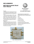
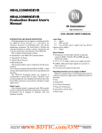
NBSG111BAEVB NBSG111 Evaluation Board User's Manual http://onsemi.com EVAL BOARD USER’S MANUAL Description What measurements can you expect to make? This document describes the NBSG111 evaluation board and the appropriate lab test setups. It should be used in conjunction with the NBSG111 data sheet which contains full technical details on the device specifications and operation. The evaluation board is designed to facilitate a quick evaluation of the NBSG111 GigaCommt 1:10 clock data driver. The NBSG111 allows selection between two inputs and fan out 10 identical differential outputs. The Reduced Swing ECL (RSECL) output ensures minimal noise and fast switching edges. The evaluation board is implemented in two layers for higher performance. For standard lab setup and test, a split (dual) power supply is required enabling the 50 W impedance from the scope to be used as termination of the ECL signals (VTT = VCC – 2.0 V, in split power supply setup, VTT is the system ground). With this evaluation board, the following measurements could be performed in single-ended (Note 1) or differential modes of operation: Jitter Output Skew Gain/Return Loss Eye Pattern Generation Frequency Performance Output Rise and Fall Time VIHCMR (Input High Common Mode Range) 1. Single-ended measurements can only be made at VCC − VEE = 3.3 V using this board setup. Figure 1. NBSG111 Evaluation Board Semiconductor Components Industries, LLC, 2012 March, 2012 − Rev. 1 1 Publication Order Number: EVBUM2091/D NBSG111BAEVB SETUP FOR TIME DOMAIN MEASUREMENTS Table 1. BASIC EQUIPMENT Example Equipment (Note 2) Description Quantity Power Supply with 2 outputs HP6624A 1 Oscilloscope TDS8000 with 80E01 Sampling Head (Note 3) 1 Differential Signal Generator HP 8133A, Advantest D3186 1 Matched high speed cables with SMA connectors Storm, Semflex 10 Power Supply cables with clips 3 2. Equipment used to generate example measurements within this document. 3. 50 GHz sample module used (for effective rise, fall and jitter performance measurement) Setup Step 1: Connect Power Step 2: Connect Inputs 1a: Three power levels must be provided to the board for VCC, VEE, and GND via the surface mount clips. Using the split power supply mode, GND = VTT = VCC – 2.0 V. For Differential Mode (3.3 V and 2.5 V operation) 2a: Connect the differential output of the generator to the differential input of the device (CLK0 and CLK0). For Single−Ended Mode (3.3 V operation only) 2a: Connect the AC coupled single-ended output generator to input. Table 2. POWER SUPPLY CONNECTIONS 3.3 V Setup 2.5 V Setup VCC = 2.0 V VCC = 2.0 V VTT = GND VTT = GND VEE = −1.3 V VEE = −0.5 V NOTE: For best results, unconnected input should be terminated to VTT through 50 W resistor. VCC Float VCC = 2.0 V Signal Generator VCC VTT = 0 V SEL SEL GND CLK0 Channel 1 Channel 2 Channel 3 Q0 Channel 4 OUT Q0 OUT Amplitude = 500 mV Offset = 660 mV CLK0 VEE Q9 EN GND EN Q9 TRIGGER VEE = −1.3 V (3.3 V op) −or− VEE = −0.5 V (2.5 V op) NOTE: VTT = 0 V Float VCC Digital Oscilloscope Channel 5 Channel 6 Channel 7 Channel 8 TRIGGER All differential cable pairs must be matched. Due to simplification of the block diagram CLK1/CLK1 and Q1 − Q8 connections are not shown. Figure 2. NBSG111 Board Setup − Time Domain (Differential Mode) http://onsemi.com 2 * Q0 − Q9 Ouputs NBSG111BAEVB Setup (continued) Step 3: Setup Input Signals Step 4: Connect Output Signals 3a: Set the signal generator amplitude to 500 mV. 4a: Connect the outputs of the device (Q0, Q1, ) to the Oscilloscope. The oscilloscope sampling head must have internal 50 W termination to ground. NOTE: The signal generator amplitude can vary from 75 mV to 900 mV to produce a 400 mV DUT output. 3b: Set the signal generator offset to 660 mV (the center of a nominal RSECL PECL output). NOTE: Where a single output is being used, the unconnected output for the pair must be terminated to VTT through a 50 W resistor for best operation. Unused pairs may be left unconnected. Since VTT = 0 V, a standard 50 W SMA termination is recommended. NOTE: The VIHCMR (Input High Voltage Common Mode Range) allows the signal generator offset to vary as long as VIH is within the VIHCMR range. Refer to the device data sheet for further information. 3c: Set the generator output for a PRBS data signal, or for a square wave clock signal with a 50% duty cycle. VCC VCC = 2.0 V Signal Generator VCC AC_Coupling Float VTT = 0 V SEL SEL GND CLK0 Channel 1 Channel 2 Channel 3 Q0 Channel 4 OUT Q0 OUT Amplitude = 500 mV Offset = 660 mV 50 W CLK0 VEE Q9 EN GND EN Q9 TRIGGER VTT = 0 V VEE = −1.3 V (3.3 V op) VCC NOTE: Float Digital Oscilloscope Channel 5 Channel 6 Channel 7 Channel 8 TRIGGER All differential cable pairs must be matched. Due to simplifcation of the block diagram CLK1/CLK1 and Q1 − Q8 connections are not shown. * Q0 − Q9 Outputs Figure 3. NBSG111 Board Setup − Time Domain (Single-ended Mode) http://onsemi.com 3 NBSG111BAEVB SETUP FOR FREQUENCY DOMAIN MEASUREMENTS Table 3. Basic Equipment Example Equipment (Note 4) Description Quantity Power Supply with 2 outputs HP 6624A 1 Vector Network Analyzer (VNA) R&S ZVK (10 MHz to 40 GHz) 1 180 Hybrid Coupler Krytar Model #4010180 1 Bias Tee with 50 W Resistor Termination Picosecond Model #5542−219 1 Matched high speed cables with SMA connectors Storm, Semflex 3 Power Supply cables with clips 3 4. Equipment used to generate example measurements. Setup Setup Test Configurations for Differential Operation Step 1: Connect Power A) Small Signal Setup 1a: Three power levels must be provided to the board for VCC, VEE, and GND via the surface mount clips. Using the split power supply mode, GND = VTT = VCC – 2.0 V. Step 2: Input Setup 2a: Calibrate VNA from 1.0 GHz to 12 GHz. 2b: Set input level to –35 dBm at the output of the 180 Hybrid coupler (input of the DUT). Table 4. POWER SUPPLY CONNECTIONS 3.3 V Setup 2.5 V Setup VCC = 2.0 V VCC = 2.0 V VTT = GND VTT = GND VEE = −1.3 V VEE = −0.5 V Step 3: Output Setup 3a: Set display to measure S21 and record data. B) Large Signal Setup Step 2: Input Setup NOTE: For frequency domain measurements, 2.5 V power supply is not recommended because additional equipment (bias tee, etc.) is needed for proper operation. The input signal has to be properly offset to meet VIHCMR range of the device. 2a: Calibrate VNA from 1.0 GHz to 12 GHz. 2b: Set input levels to −2.0 dBm (500 mV) at the input of DUT. Step 3: Output Setup 3a: Set display to measure S21 and record data. Vector Network Analyzer PORT 1 GND VCC = 2.0 V 50 W VCC VCC Float VTT = 0 V SEL SEL GND CLK0 180 Hybrid Coupler NOTE: All differential cable pairs must be matched. Due to simplifcation of the block diagram CLK1/CLK1 and Q1 − Q8 connections are not shown. PORT 2 GND 50 W Bias T Q0 Q0 50 W GND 50 W Q9 CLK0 VEE EN VEE = −1.3 V (3.3 V op) EN GND Q9 VTT = 0 V VCC Float GND 50 W GND * Q0 − Q9 Outputs Figure 4. NBSG111 Board Setup – Frequency Domain (Differential Mode) http://onsemi.com 4 NBSG111BAEVB Setup Test Configurations for Single-ended Operation A) Single-ended Mode − Small Signal B) Single-ended Mode − Large Signal Step 2: Input Setup Step 2: Input Setup 2a: Calibrate VNA from 1.0 GHz to 12 GHz. 2b: Set input level to –35 dBm at the input of DUT. 2a: Calibrate VNA from 1.0 GHz to 12 GHz. 2b: Set input levels to +2 dBm (500 mV) at the input of DUT. Step 3: Output Setup Step 3: Output Setup 3a: Set display to measure S21 and record data. 3a: Set display to measure S21 and record data. Vector Network Analyzer PORT 1 PORT 2 Float VCC GND VCC = 2.0 V VTT = 0 V SEL VCC SEL GND CLK0 50 W Bias T Q0 Q0 50 W GND 50 W Q9 CLK0 VEE EN GND EN GND Q9 VTT = 0 V VEE = −1.3 V (3.3 V op) VCC NOTE: 50 W GND 50 W GND Float All differential cable pairs must be matched. Due to simplifcation of the block diagram CLK1/CLK1 and Q1 − Q8 connections are not shown. * Q0 − Q9 Outputs Figure 5. NBSG111 Board Setup – Frequency Domain (Single-ended Mode) http://onsemi.com 5 NBSG111BAEVB MORE INFORMATION ABOUT EVALUATION BOARD Design Considerations for >10 GHz operation The following considerations played a key role to ensure this evaluation board achieves high−end microwave performance: Optimal SMA connector launch Minimal insertion loss and signal dispersion Accurate Transmission line matching (50 ohms) Distributed effects while bypassing and noise filtering While the NBSG111 is specified to operate at 12 GHz, this evaluation board is designed to support operating frequencies up to 20 GHz. Surface Mount Clip VCC T2 T6 VTEN T2 0 Surface Mount Clip 1 T7 Open Circuit Stub EN T7 T2 T3 EN T4 Surface Mount Clip 1 VTEN T2 0 C2 0 VTCLK0 0 ROSENBERGER SMA ROSENBERGER SMA 1 1 T1 T2 CLK0 T2 VTCLK0 ROSENBERGER SMA ROSENBERGER SMA NBSG111 VTCLK1 0 T1 1 T1 1 T8 1 1 1 1 1 T2 1 T2 T4 0 SEL SEL C1 VTSEL C1, C2 = Decoupling Cap Tx = 50 W Transmision Line 1 0 T2 T2 T3 0 NOTE: 1 1 T5 Surface Mount Clip 1 1 T2 VTSEL T8 1 T2 T2 CLK1 0 1 1 T2 CLK1 VTCLK Surface Mount Clip 1 1 0 1 T2 T2 CLK0 T1 T2 1 Open Circuit Stub T2 T2 T2 VEE Surface Mount Clip 1 1 1 1 Q0 − Q9 Outputs Figure 6. Evaluation Board Schematic http://onsemi.com 6 ROSENBERGER SMA ROSENBERGER SMA ROSENBERGER SMA ROSENBERGER SMA ROSENBERGER SMA ROSENBERGER SMA ROSENBERGER SMA ROSENBERGER SMA ROSENBERGER SMA ROSENBERGER SMA ROSENBERGER SMA ROSENBERGER SMA ROSENBERGER SMA ROSENBERGER SMA ROSENBERGER SMA ROSENBERGER SMA ROSENBERGER SMA ROSENBERGER SMA ROSENBERGER SMA ROSENBERGER SMA NBSG111BAEVB Table 5. PARTS LIST Part No Description Manufacturer Web Address NBSG111BA 2.5V/3.3V SiGe Differential 1:10 Clock/Data Driver with RSECL Outputs ON Semiconductor http://www.onsemi.com/NBSG111 32K243−40ME3 Gold plated connector Rosenberger http://www.rosenberger.de CO6BLBB2X5UX 2 MHz – 30 GHz capacitor Dielectric Laboratories http://www.dilabs.com Table 6. BOARD MATERIAL Material Thickness Rogers 6002 5.0 mil Copper Plating 32 mil 12.5 mil 1.37 mil Dielectric (5.0 mil) Thick Copper Base Figure 7. Board Stack-up PIN 1 Figure 8. Layout Mask for NBSG111 http://onsemi.com 7 NBSG111BAEVB EXAMPLE MEASUREMENTS IN TIME DOMAIN 10.0 9.0 8.0 Q AMP (mV) 450 7.0 6.0 3.3 V 350 5.0 4.0 2.5 V RMS JITTER (ps) OUTPUT VOLTAGE AMPLITUDE (mV) 550 3.0 250 2.0 RMS JITTER (ps) 150 1 2 1.0 3 4 5 6 0.0 INPUT FREQUENCY (GHz) Figure 9. Output Voltage Amplitude (VOUTPP) / RMS Jitter vs. Input Frequency (fin) at Ambient Temperature (Typical) Figure 10. NBSG111: Eye Diagram at 6 Gbps with PRBS 2^31−1 (Total Pk−Pk system jitter including signal generator is 28 ps. Device Pk−Pk jitter is typically 14 ps.) http://onsemi.com 8 NBSG111BAEVB ADDITIONAL EVALUATION BOARD INFORMATION www.onsemi.com References In all cases, the most up-to-date information can be found on our website. Sample orders for devices and boards New Product updates Literature download/order IBIS and Spice models NBSG111/D, Data Sheet, NBSG111, 2.5 V/3.3 V SiGe 1:10 Differential Clock/Data Driver with RSECL Outputs AND8077/D, Application Note, GigaCommE (SiGe) SPICE Modeling Kit. AND8075/D, Application Note, Board Mounting Considerations for the FCBGA Packages. Table 7. ORDERING INFORMATION Description Package Shipping† NBSG111BA 2.5 V/3.3 V SiGe Differential 1:10 Clock/Data Driver with RSECL Outputs 4x4 mm FCBGA−49 100 Units/Tray NBSG111BA 2.5 V/3.3 V SiGe Differential 1:10 Clock/Data Driver with RSECL Outputs 4x4 mm FCBGA−49 500 Units/Reel NBSG111BAEVB NBSG111 Evaluation Board Orderable Part No †For information on tape and reel specifications, including part orientation and tape sizes, please refer to our Tape and Reel Packaging Specification Brochure, BRD8011/D. http://onsemi.com 9 NBSG111BAEVB PACKAGE DIMENSIONS FCBGA−49 BA SUFFIX PLASTIC 8x8 mm (1.0 mm pitch) BGA FLIP CHIP PACKAGE CASE 489A−02 ISSUE A A B NOTES: 1. CONTROLLING DIMENSION: MILLIMETER. 2. DIMENSIONS AND TOLERANCES PER ASME Y14.5M-1994. 3. DIMENSION b IS MEASURED AT THE MAXIMUM SOLDER BALL DIAMETER, PARALLEL TO DATUM PLANE C. 4. DATUM C (SEATING PLANE) IS DEFINED BY THE SPHERICAL CROWNS OF THE SOLDER BALLS. 5. PARALLELISM MEASUREMENT SHALL EXCLUDE ANY EFFECT OF MARK ON TOP SURFACE OF PACKAGE. 6. 489A-01 OBSOLETE, NEW STANDARD 489A-02. A D A2 ÉÉ ÉÉ TERMINAL A1 CORNER Z E 4X Z DETAIL A 0.15 C D1 e FEDUCIAL FOR PIN A1 IDENTIFICATION IN THIS AREA NOTE 5 A B e E1 49 X 0.20 C b NOTE 3 C 0.15 M C A B D 0.08 M C E NOTE 4 0.12 C G 6 5 4 3 2 C SEATING PLANE F 7 MILLIMETERS MIN MAX --1.40 0.3 0.5 0.91 REF 0.40 0.60 8.00 BSC 6.00 BSC 8.00 BSC 6.00 BSC 1.00 BSC DIM A A1 A2 b D D1 E E1 e 49 X 1 A1 DETAIL A (ROTATED 90 _ C.W.) VIEW Z−Z GigaComm is a trademark of Semiconductor Components Industries, LLC. ON Semiconductor and are registered trademarks of Semiconductor Components Industries, LLC (SCILLC). SCILLC reserves the right to make changes without further notice to any products herein. SCILLC makes no warranty, representation or guarantee regarding the suitability of its products for any particular purpose, nor does SCILLC assume any liability arising out of the application or use of any product or circuit, and specifically disclaims any and all liability, including without limitation special, consequential or incidental damages. “Typical” parameters which may be provided in SCILLC data sheets and/or specifications can and do vary in different applications and actual performance may vary over time. All operating parameters, including “Typicals” must be validated for each customer application by customer’s technical experts. SCILLC does not convey any license under its patent rights nor the rights of others. SCILLC products are not designed, intended, or authorized for use as components in systems intended for surgical implant into the body, or other applications intended to support or sustain life, or for any other application in which the failure of the SCILLC product could create a situation where personal injury or death may occur. Should Buyer purchase or use SCILLC products for any such unintended or unauthorized application, Buyer shall indemnify and hold SCILLC and its officers, employees, subsidiaries, affiliates, and distributors harmless against all claims, costs, damages, and expenses, and reasonable attorney fees arising out of, directly or indirectly, any claim of personal injury or death associated with such unintended or unauthorized use, even if such claim alleges that SCILLC was negligent regarding the design or manufacture of the part. SCILLC is an Equal Opportunity/Affirmative Action Employer. This literature is subject to all applicable copyright laws and is not for resale in any manner. PUBLICATION ORDERING INFORMATION LITERATURE FULFILLMENT: Literature Distribution Center for ON Semiconductor P.O. Box 5163, Denver, Colorado 80217 USA Phone: 303−675−2175 or 800−344−3860 Toll Free USA/Canada Fax: 303−675−2176 or 800−344−3867 Toll Free USA/Canada Email: [email protected] N. American Technical Support: 800−282−9855 Toll Free USA/Canada Europe, Middle East and Africa Technical Support: Phone: 421 33 790 2910 Japan Customer Focus Center Phone: 81−3−5817−1050 http://onsemi.com 10 ON Semiconductor Website: www.onsemi.com Order Literature: http://www.onsemi.com/orderlit For additional information, please contact your local Sales Representative EVBUM2091/D