1
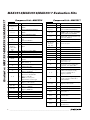
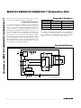
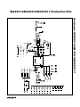
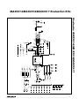
19-1826; Rev 0; 3/01
MAX3514/MAX3516/MAX3517 Evaluation Kits
Access to the device input and output is provided
through 50Ω SMA connectors. The input is matched to
50Ω, while the output circuit includes a minimum-loss
pad that presents a 75Ω load to the output transformer
when using 50Ω test equipment.
Windows is a registered trademark of Microsoft Corp.
Features
♦ +5V Single-Supply Operation
♦ Output Level Range up to 64dBmV (QPSK)
♦ Gain Programmable in 0.5dB Steps
♦ Transmit-Disable Mode
♦ Shutdown Mode
♦ Control Software Included
♦ Fully Assembled and Tested Surface-Mount
Board
Ordering Information
PART
TEMP RANGE
IC PACKAGE
MAX3514EVKIT
-40°C to +85°C
20 QSOP
MAX3516EVKIT
-40°C to +85°C
20 TSSOP-EP*
MAX3517EVKIT
-40°C to +85°C
20 QSOP
* Exposed paddle.
Component List—MAX3514
DESIGNATION
QTY
C1, C6
2
C2, C5, C8,
C9, C11
5
DESCRIPTION
QTY
T2
1
Transformer 2 to 1 voltage ratio,
type B5F
Toko 348PT-1087
U1
1
MAX3514EEP 20-pin QSOP
J1
1
SMA connector (PC mount)
Johnson 142-0701-201 or
Digi-Key J502-ND
J2
1
DB25 connector, right angle –
female
Digi-Key A2102-ND or
AMP 745783-4
JU1–JU7
7
1 ✕ 3 pin headers (0.1in centers)
Digi-Key S1012-36-ND
Leave site open
0.1µF ±10% ceramic capacitors
(0603)
Murata GRM39X7R104K016A
C3, C4
2
1000pF ±10% ceramic capacitors
(0603)
Murata GRM39X7R102K050A
C7
1
10µF ±10%, 16V min tantalum
capacitor
AVX TAJC106K016
R1
1
49.9Ω ±1% resistor (0603)
R2, R3, R4,
R6–R13,
R16–R19
15
Leave site open
R5
1
43.2Ω ±1% resistor (0805)
R14, R15
2
100kΩ ±5% resistors (0603)
R21
1
86.6Ω ±1% resistor (0805)
L1
1
0Ω resistor (0805)
B3–B6
4
Murata BLM21A601RPT
1
Transformer 1 to 1
Macom ECT1-1T
T1
DESIGNATION
DESCRIPTION
JU1–JU7
7
Shunts, Digi-Key S9000-ND
IN1, IN2
2
Test points, Digi-Key 5000K-ND
None
1
MAX3514/MAX3517 EV kit circuit
board, Rev. 2
None
1
MAX3514/MAX3516/MAX3517
software disk
None
1
MAX3514/MAX3516/MAX3517
data sheet
None
1
MAX3514/MAX3516/MAX3517 EV
kit data sheet
________________________________________________________________ Maxim Integrated Products
For pricing, delivery, and ordering information, please contact Maxim/Dallas Direct! at
1-888-629-4642, or visit Maxim’s website at www.maxim-ic.com.
1
Evaluate: MAX3514/MAX3516/MAX3517
General Description
The MAX3514/MAX3516/MAX3517 evaluation kits (EV
kits) simplify evaluation of the MAX3514/MAX3516/
MAX3517 CATV upstream amplifiers. Each kit includes
a data interface that can be programmed through the
parallel port of a standard PC. Software (Windows®
95/98 compatible) is included to facilitate this function.
This software allows the user to program both the gain
and transmit modes through a simple user interface.
Evaluate: MAX3514/MAX3516/MAX3517
MAX3514/MAX3516/MAX3517 Evaluation Kits
Component List—MAX3516
DESIGNATION
QTY
C1, C4, C6, C8,
C9
5
C2, C3
2
C5, C10
2
C7
1
R1
R2, R3, R4,
R6–R13,
R16–R19, R22,
R23
R5
R14, R15
R21
B1, B2
1
B3–B6
1
2
1
2
4
T1
1
T2
1
U1
1
J2
1
J1, J3
JU1–JU7
2
17
2
7
JU1–JU7
7
IN1, IN2
2
None
None
None
None
1
1
1
1
DESCRIPTION
0.1µF ±10% ceramic capacitors
(0805)
Murata GRM40X7R104K016A
1000pF ±10% ceramic capacitors
(0805)
Murata GRM40102K050A
Open
10µF tantalum capacitor ±10%, 16V
min
AVX TAJC106K016
49.9 Ω ±1% resistor (0402)
Open
43.2Ω ±1% resistor (0805)
100kΩ ±5% resistors (0805)
86.6Ω ± 1% resistor (0805)
0Ω resistors (0805)
BLM21A601RPT
Murata
1-to-1 transformer
Macom ETC1-1T
4-to-1 transformer type B5F
TOKO 458PT-1087
MAX3516EUP, 20-pin TSSOP-EP
DB25 connector, right angle, female
Digi-Key A2102-ND
SMA connectors (edge mount)
EFJohnson 142-0701-801
Digi-Key J502-ND
Note: Cut center pin to
approximately 1/16in length.
1 x 3 pin headers (0.1in centers)
Digi-Key S1012-36-ND
Shunts
Digi-Key S9000-ND
Test points
Digi-Key 5000K-ND
MAX3516 EV kit circuit board, Rev A
MAX3514 software disk
MAX3516 data sheet
MAX3516 EV kit data sheet
Component List—MAX3517
DESIGNATION
QTY
C1, C6
DESCRIPTION
2
Leave site open
C2, C5, C8,
C9, C11
5
0.1µF ±10% ceramic caps (0603)
Murata GRM39X7R104K016A
C3, C4
2
1000pF ±10% ceramic caps (0603)
Murata GRM39X7R102K050A
C7
1
10µF ±10%, 16V min tantalum cap
AVX TAJC106K016
R1
1
49.9Ω ±1% resistor (0603)
R2, R3, R4,
R6–R13,
R18, R19
13
Leave site open
R5
1
43.2Ω ±1% resistor (0805)
R14, R15
2
100kΩ ±5% resistors (0603)
R16, R17
2
300Ω ±5% resistors (0603)
R21
1
86.6Ω ±1% resistor (0805)
L1
1
0Ω resistor (0805)
B3–B6
4
Murata BLM21A601RPT
T1
1
Transformer 1 to 1
Macom ECT1-1T
T2
1
Transformer 2 to 1 voltage ratio,
type B5F, Toko 348PT-1087
U1
1
MAX3517EEP 20-pin QSOP
J1, J3
2
SMA connectors (PC mount)
Johnson 142-0701-201 or
Digi-Key J502-ND
J2
1
DB25 connector, right angle –
female, Digi-Key A2102-ND or
AMP 745783-4
JU1–JU7
7
1 ✕ 3 pin headers (0.1in centers)
Digi-Key S1012-36-ND
JU1–JU7
7
Shunts, Digi-Key S9000-ND
IN1, IN2
2
Test points, Digi-Key 5000K-ND
None
1
MAX3514/MAX3517 EV kit circuit
board, Rev. 2
None
1
MAX3514/MAX3516/MAX3517
software disk
None
1
MAX3514/MAX3516/MAX3517
data sheet
None
1
MAX3514/MAX3516/MAX3517 EV
kit data sheet
_______________________________________________________________________________________
MAX3514/MAX3516/MAX3517 Evaluation Kits
JUMPER
FUNCTION
JU1
Set the method of control of SHDN
JU2
Set the manual control state of SHDN
JU3
Set the method of control of TXEN
JU4
Set the manual control state of TXEN
JU5
JU6
JU7
SHORT PIN1 TO PIN2
SHORT PIN2 TO PIN3
PC port control
Manual control through JU2
Logic 1 state (VCC)
Logic 0 state (GND)
PC port control
Manual control through JU4
Logic 1 state (VCC)
Logic 0 state (GND)
CS input
PC port control
N/A
SDA input
PC port control
N/A
SCLK input
PC port control
N/A
Quick Start
The MAX3514/MAX3516/MAX3517 EV kits are fully
assembled and factory tested. Follow the instructions in
the Connections and Setup section. Note: The output
circuit includes a minimum-loss pad that is used to
bring the load impedance up to 75Ω. This must be
accounted for in all measurements (see Output Circuit
section).
Note: The input transformer is supplied to allow differential input drive from a single-ended source. A transformer is not required in the application.
Test Equipment Required
• DC supply capable of delivering 5.5V and 200mA of
continuous current
• HP 8648 or equivalent signal source capable of generating 40dBmV up to 200MHz
• HP 8561E or equivalent spectrum analyzer with a
minimum 200MHz frequency range
• Digital multimeter (DMM) to monitor VCC and ICC, if
desired
• Lowpass filters to attenuate harmonic output of signal sources, if harmonic measurements are desired
• Network analyzer, such as the HP 8753D (may be
used to measure gain and harmonic levels if configured with this option; contact test equipment manufacturer)
Table 2. MAX3514/MAX3616/MAX3517
EV Kit Software
FILENAME
DESCRIPTION
Max3514.txt
“Read Me” text file
Max3514.exe
Windows executable
Max3510.dll
DLL file for printer port control
Msvbvm50.dll
DLL file
pins labeled +5V and GND on the circuit board.
Connect a 50Ω signal source to INPUT (preset the
signal source for -13dBm (+34dBmV across a 50Ω
load)), and terminate OUTPUT with a spectrum analyzer or network analyzer having a 50Ω input impedance. If using a signal source with a source impedance other than 50Ω, or if a different input impedance is required, be sure to replace resistor R1 with
the appropriate value resistor.
2) Connect a 25-pin male-to-male cable between the
parallel (printer) port of the PC and the 25-pin
female connector on the EV kit board.
3) See Table 1 for board jumper settings.
4) Turn on the power supply. Turn on the PC and the
test equipment.
5) Run the software program.
Detailed Description
• IBM PC or compatible with Windows 95/98 installed
Using the Software
• Male-to-male 25-pin parallel cable, straight through
The MAX3514/MAX3516/MAX3517 use a serial data
interface (SDI) to set gain. Some means of communicating with the SDI is required to use the MAX3514/
MAX3516/MAX3517 EV kits. A microprocessor, pattern
generator, or PC can be used for this function.
Software is included in these EV kits to facilitate the use
of a PC.
• 0 to 5V pulse generator (transient measurement)
• Low-noise amplifier with 40dB gain from 5MHz to
100MHz (noise measurement)
• Oscilloscope with 200MHz bandwidth
Connections and Setup
1) Connect the power supply (preset to +5V) to the
_______________________________________________________________________________________
3
Evaluate: MAX3514/MAX3516/MAX3517
Table 1. Jumper Setting Functions
Evaluate: MAX3514/MAX3516/MAX3517
MAX3514/MAX3516/MAX3517 Evaluation Kits
The disks included with the MAX3514/MAX3516/
MAX3517 EV kits contain four files each. Table 2 lists
these files and their appropriate usage. If your PC has
Windows 95/98 installed, run MAX3514.EXE. The software can also be found on the Maxim website.
Gain Adjustment
The valid gain code ranges from 0 to 127 (decimal).
The nominal change in gain is 0.5dB per gain code.
Gain codes are set exclusively by programming the
SDI. Refer to the MAX3514/MAX3516/MAX3517 data
sheet for details.
High Power and Low Noise
High-power (HP) mode and low-noise (LN) mode may
only be controlled via the PC interface. Manual control
of the jumpers for the EV kits’ boards is not possible.
For DOCSIS applications, HP mode should be used for
output levels above 42dBmV. This corresponds to gain
code 87. LN mode should be used below this output
level. This corresponds to gain code 115. A transition
from HP mode, gain code 87, to LN mode, gain code
117, will result in a -1dB step.
Shutdown and Transmit Enable
Jumpers JU1 through JU4 determine how the shutdown
and transmit-enable features are controlled. Pin 2 of
JU2 and pin 2 of JU4 are connected directly to the
device. If an external source (such as a modulator chip
or microprocessor) is used to control these features,
make the connections to pin 2 of JU2 and pin 2 of JU4.
Pads are provided on the board (R18 and R19, respectively) for placement of termination resistors, if needed.
If manual control of shutdown and transmit enable is
desired, shunt pins 2 and 3 of jumper JU1 and pins 2
and 3 of jumper JU3. This will allow SHDN and TXEN to
be controlled by JU2 and JU4, respectively. JU2 and
JU4 are used to place either VCC or ground at SHDN or
TXEN. Pin 3 of JU2 and pin 3 of JU4 are ground, and
pin 1 is VCC.
To control the SHDN and TXEN features using the software, shunt pin 1 and pin 2 of JU1 and JU3.
Manual Control of Serial Data Interface
If using a source other than a PC to drive the serial data
interface of the MAX3514/MAX3516/MAX3517 EV kits
(such as a digital pattern generator or microprocessor),
remove the shunts on jumpers JU5, JU6, and JU7.
Access to the serial data interface is available through
these jumpers. Termination pads are provided (R2, R3,
R4). Solder an appropriate resistor to these pads, if
desired. Refer to the MAX3514/MAX3516/MAX3517
data sheet for a description of the serial data interface.
4
To control the SDI using the software, shunt pin 1 and
pin 2 of JU5, JU6, and JU7.
Input Circuit
The input circuits of the MAX3514/MAX3516/MAX3517
EV kits are configured with a 1:1 transformer (T1) and a
49.9Ω input resistor. This allows the input to be driven
with single-ended 50Ω test equipment. The transformer
(T1) is used to generate a differential signal, as rated
performance is specified with a differential input drive
(typically from a differential lowpass filter).
If the MAX3514/MAX3516/MAX3517 are to be driven
single ended, the input transformer (T1) must be
removed and the undriven input connected to ground
through a 0.1µF blocking capacitor.
Output Circuit
The MAX3514/MAX3516/MAX3517 have differential outputs. This architecture aids in suppressing secondorder distortion (harmonics). To convert to a singleended output, a 2:1 voltage ratio transformer (T2) is
used. Since most test equipment is supplied with a 50Ω
termination impedance, a minimum-loss pad is provided on the output of the transformer to increase the load
impedance to a nominal 75Ω. This places the proper
load on the device, but will also reduce the measured
output voltage level by 7.5dB. It is essential to consider
this when making any measurements with the EV kit;
7.5dB must be added to all measurements of voltage
gain and output voltage level (including noise) to arrive
at the correct value for a 75Ω system.
Use 75Ω test equipment, if available, and take the following steps:
1) Remove the 50Ω output SMA connector and replace
it with a 75Ω connector.
2) Remove R5 and replace it with a 0Ω resistor or some
other type of shunt.
3) Remove R21.
4) Be sure to use a 75Ω cable.
Analysis
Harmonic Distortion
A filter will be needed to reject the harmonics generated
by the signal source. For this example, a lowpass filter
with approximately a 25MHz to 35MHz cutoff frequency
will be required. This filter will need to reject at least
20dB of signal at 40MHz. Set the 50Ω signal source for
20MHz and -13dBm. Adjust the amplitude to account for
the insertion loss in the filter. Verify with the spectrum
analyzer that the second and third harmonics generated
by the source are suppressed by at least 70dBc.
_______________________________________________________________________________________
MAX3514/MAX3516/MAX3517 Evaluation Kits
Connect a spectrum analyzer to OUTPUT. Set the center frequency for 40MHz and the span for 50MHz or
more. Adjust the reference level so that the fundamental (20MHz tone) is within 10dB to 20dB of the reference level. If the fundamental is less than 10dB below
the reference level, the harmonic distortion of the spectrum analyzer may prevent accurate measurement of
the distortion.
Set the gain code to 125, D7 = 1 (approximately 27dB
of gain). Measure the level of the fundamental, second,
and third harmonics on the spectrum analyzer. These
readings have units of dBm. To convert from dBm to
dBmV in a 50Ω system, use the following equation:
X (dBmV) = Y(dBm) + 47dB (50Ω system)
Add 7.5dB to this value to account for the attenuation of
the minimum-loss pad, in dBmV, for a 75Ω load. The
gain can now be calculated in dB, and the harmonic
distortion can be calculated in dBc.
Switching Transients
To measure the transmit-enable and transmit-disable
transients, the TXEN pin will be driven from an external
source. No input signal is applied, and the output is
viewed on an oscilloscope.
Connect OUTPUT to the oscilloscope’s 50Ω input. Set
the scope’s time base to 5µs/div and the vertical scale
to 5mV/div.
Set the pulse generator as follows:
• Amplitude: 5V
• Duty cycle: 50%
• Rise/fall-time: 100ns
• Pulse width: 25µs
• Offset: 2.5V
Output Noise
To measure output noise, a spectrum analyzer is used.
A postamplifier with less than 10dB noise figure and
greater than 40dB gain within the band of interest is
needed.
With the power supply off, place a 50Ω termination on
the input of the EV kit.
Turn on the powers supply to the MAX3514/MAX3516/
MAX3517 EV kits. Using the software, set the device to
transmit mode with a gain code of 119, D7 = 1 (approximately 24dB of gain, MAX3514). Connect the output of
the postamplifier to the spectrum analyzer and the
input to OUTPUT on the EV kit. Set the spectrum analyzer as follows:
• Center frequency: 35MHz
• Span: 60MHz
• Reference: -50dBm
• Scale: 10dB/div
• IF bandwidth: 1kHz
Power up the postamplifier.
If the spectrum analyzer being used has a noise marker
function, enable it. The output noise can now be read
directly from the spectrum analyzer. Move this marker
to 42MHz. Read the value of the noise density from the
spectrum analyzer. This noise value is a combination of
the output noise of the MAX3514/MAX3516/MAX3517,
the gain of the postamplifier, and the noise figure of the
postamplifier. With the specified noise figure of 10dB,
the noise contribution of the postamplifier may be
ignored. The minimum-loss pad reduces the actual
measured value by 7.5dB. Use the following equation
to arrive at the MAX3514/MAX3516/MAX3517s’ output
noise in a 160kHz bandwidth:
VNOISE = PNOISE + 47dB + 7.5dB + 10 ✕ log
(160,000) - GAMP
where:
Take care not to drive the MAX3514/MAX3516/
MAX3517 TXEN pin below 0 or above +5V. Turn on the
power supply. Remove the shunt from jumper JU3
(TXEN), and connect the output of the pulse generator
to pin 2 of this jumper. Trigger the oscilloscope from
the pulse generator using a convenient method.
Set the gain code to 125, D7 = 1.
A rising- and falling-edge transient should appear on
the scope’s CRT. The amplitude of this transient should
be less than 40mVp-p. Multiply the value of the measured transient by 2.37 to account for the presence of
the minimum-loss pad. The gain may now be changed
to show the output transient’s dependence on gain.
VNOISE = MAX3514/MAX3516/MAX3517 output
noise in dBmV measured in a 160kHz bandwidth
PNOISE = Noise density in dBm/Hz read from the
spectrum analyzer
GAMP = Gain of the postamplifier in dB
If the spectrum analyzer being used does not have a
noise marker function, corrections must be made to
account for the IF bandwidth used to make the measurement. Consult the user’s manual for your spectrum
analyzer for details. Once the correction is made, the
value read from the spectrum analyzer can be converted to a noise density (dBm/Hz), and the above formula
can be used.
_______________________________________________________________________________________
5
Evaluate: MAX3514/MAX3516/MAX3517
Connect the filter between INPUT of the EV kit and the
output of the signal source, making sure the proper terminations are being used for this particular filter.
Evaluate: MAX3514/MAX3516/MAX3517
MAX3514/MAX3516/MAX3517 Evaluation Kits
Noise can now be measured at various gains. Output
noise in transmit-disable mode is insignificant.
Component Suppliers
SUPPLIER
AVX
M/A-COM
Murata
TOKO
Layout Considerations
The MAX3514/MAX3516/MAX3517 evaluation board
can serve as a guide for your board layout. Particular
attention should be paid to thermal design and to the
output network. The MAX3514/MAX3516/MAX3517
package exposed paddle (EP) conducts heat out of the
part and also provides a low-impedance electrical connection. The EP must be attached to the PC board
ground plane with a low thermal and electrical impedance contact. Ideally, this would be provided by soldering the backside package contact directly to a top
metal ground plane on the PC board. Alternatively, the
EP could be connected to a ground plane using an
array of plated vias directly below EP.
PHONE
803-946-0690
978-442-5000
814-237-1431
847-297-0076
FAX
803-626-3123
978-442-4178
814-238-0490
847-297-7864
The output circuit that connects OUT+ and OUT- (pins
15 and 16) to the output transformer (T2) should be as
symmetrical as possible to reduce second-order distortion. In addition, the capacitance of this path should be
kept low to minimize gain rolloff at high frequencies.
Functional Diagram
TXEN
SHDN
VCC
BIAS
CONTROL
MAX3514
MAX3516
MAX3517
HIGH
POWER
OUTCEXT
IN+
OUT+
INLOW
NOISE
D/A CONVERTER
SERIAL DATA INTERFACE
CS SDA SCLK
6
GND
*MAX3514/MAX3516 ONLY
_______________________________________________________________________________________
*
J2-17
J2-16
J2-14
J2-12
J2-11
J2-9
J2-8
J2-1
IN2
J2-25
J2-24
J2-23
J2-22
J2-21
J2-20
J2-19
J2-18
R13
OPEN
R12
OPEN
R11
OPEN
R10
OPEN
R9
OPEN
R8
OPEN
R7
OPEN
R6
OPEN
C7
10µF
SMA
R1
49.9Ω
INPUT
J1
J2-4
J2-3
J2-2
4
5
T1
1
2
3
R4
OPEN
MAX3514
U1
20
19
18
17
16
15
14
13
12
11
R18
OPEN
GND
VCC2
TXEN
N.C.
OUT+
OUTCEXT
NC
SHDN
GND
C5
0.1µF
J2-5
C1
OPEN
C11
0.1µF
1
JU7
R16
OPEN
2
2
1
C9
0.1µF
VCC
R17
OPEN
T2
4
5
TOKO458PT-1087
B3 BLM21A601RPT 3
VCC3
JU4
VCC
JU1
GND
VCC1
GND
GND
IN+
INGND
CS
SDA
SCLK
R19
OPEN
VCC2
TXEN
JU3
VCC
JU6
1
2
3
4
5
6
7
8
9
10
J2-6
J2-15
R15
100kΩ
SHDN
JU2
R3
OPEN
C2
0.1µF
VCC3
VCC2
VCC1
J2-10
J2-13
JU5
R2
OPEN
C3
1000pF
C4
1000pF
VCC1
B6 BLM21A601RPT
M/A COM ETC1-1T
C8
0.1µF
B5 BLM21A601RPT
VCC
R14
100kΩ
1
L1
C6
OPEN
0
IND0805
2
R5
43.2Ω
R21
86.6Ω
SMA
OUTPUT
J3
Evaluate: MAX3514/MAX3516/MAX3517
IN1
B4 BLM21A601RPT
J2-7
MAX3514/MAX3516/MAX3517 Evaluation Kits
Figure 1. MAX3514 EV Kit Schematic
_______________________________________________________________________________________
7
8
J2-17
J2-16
J2-14
J2-12
J2-11
J2-9
J2-8
J2-1
Figure 2. MAX3516 EV Kit Schematic
_______________________________________________________________________________________
J2-25
J2-24
J2-23
J2-22
J2-21
J2-20
J2-19
J2-18
R13
OPEN
R12
OPEN
R11
OPEN
R10
OPEN
R9
OPEN
R8
OPEN
R7
OPEN
R6
OPEN
IN2
IN1
J1
R1
49.9Ω
INPUT
SMA
J2-4
J2-3
J2-2
C7
10µF
T1
6
5
4
JU7
JU6
JU5
R17
OPEN
R2
OPEN
R3
OPEN
C3
1000pF
C1
0.1µF
B2
0Ω
B6 BLM21A601RPT
B5 BLM21A601RPT
C2
1000pF
VCC1
C8
0.1µF
M/A COM ETC1-1T
1
2
3
R16
OPEN
B1
0Ω
B4 BLM21A601RPT
1
2
3
4
5
6
7
8
9
10
R4
OPEN
J2-6
R15
100kΩ
1
×200
MTHOLE2
1
MTHOLE2
1
SHDN
JU1
1
×400
MTHOLE2
C9
0.1µF
R23
OPEN
×300
1
VCC
VCC
2
JU4
2
1
T2
4
5
6
LOGO
×36
1
JU2
TOKO 458PT-1087
B3 BLM21A601RPT 3
VCC3
R19
OPEN
J2-13
MTHOLE2
JU3
TXEN
R18
OPEN
J2-5
C10
OPEN
C6
0.1µF
20
VCC3
19
18
OPEN
17 C5
16
15
14
13
C4
12
R22
0.1µF
11
OPEN
J2-15
J2-10
R14
100kΩ
×100
GND
GND
U1
VCC
VCC
GND
TXEN
MAX3516EUP
GND
N.C.
IN+
OUT+
INOUTGND
CEXT
CS
NC
SDA
SHDN
GND
SCLK
VCC3
VCC2
VCC1
VCC
J2-7
VCC
R5
43.2Ω
SMA
OUTPUT
R21
86.6Ω
J3
Evaluate: MAX3514/MAX3516/MAX3517
MAX3514/MAX3516/MAX3517 Evaluation Kits
J2-17
J2-16
J2-14
J2-12
J2-11
J2-9
J2-8
J2-1
IN2
J2-25
J2-24
J2-23
J2-22
J2-21
J2-20
J2-19
J2-18
R13
OPEN
R12
OPEN
R11
OPEN
R10
OPEN
R9
OPEN
R8
OPEN
R7
OPEN
R6
OPEN
C7
10µF
SMA
R1
49.9Ω
INPUT
J1
J2-4
J2-3
J2-2
4
5
T1
1
2
3
R4
OPEN
MAX3517
U1
20
19
18
17
16
15
14
13
12
11
R18
OPEN
GND
VCC2
TXEN
N.C.
OUT+
OUTCEXT
NC
SHDN
GND
C5
0.1µF
J2-5
C1
OPEN
C11
0.1µF
1
JU7
R16
300Ω
2
2
1
C9
0.1µF
VCC
R17
300Ω
T2
4
5
TOKO458PT-1087
B3 BLM21A601RPT 3
VCC3
JU4
VCC
JU1
GND
VCC1
GND
GND
IN+
INGND
CS
SDA
SCLK
R19
OPEN
VCC2
TXEN
JU3
VCC
JU6
1
2
3
4
5
6
7
8
9
10
J2-6
J2-15
R15
100kΩ
SHDN
JU2
R3
OPEN
C2
0.1µF
VCC3
VCC2
VCC1
J2-10
J2-13
JU5
R2
OPEN
C3
1000pF
C4
1000pF
VCC1
B6 BLM21A601RPT
M/A COM ETC1-1T
C8
0.1µF
B5 BLM21A601RPT
VCC
R14
100kΩ
1
L1
C6
OPEN
0
IND0805
2
R5
43.2Ω
R21
86.6Ω
SMA
OUTPUT
J3
Evaluate: MAX3514/MAX3516/MAX3517
IN1
B4 BLM21A601RPT
J2-7
MAX3514/MAX3516/MAX3517 Evaluation Kits
Figure 3. MAX3517 EV Kit Schematic
_______________________________________________________________________________________
9
Evaluate: MAX3514/MAX3516/MAX3517
MAX3514/MAX3516/MAX3517 Evaluation Kits
1.0"
Figure 4. MAX3514/MAX3517 EV Kit Component Placement
Guide—Component Side
1.0"
Figure 6. MAX3514/MAX3517 EV Kit PC Board Layout—Solder
Side
10
1.0"
Figure 5. MAX3514/MAX3517 EV Kit PC Board Layout—Solder
Side
1.0"
Figure 7. MAX3516 EV Kit Component Placement Guide—
Component Side
______________________________________________________________________________________
MAX3514/MAX3516/MAX3517 Evaluation Kits
1.0"
Figure 8. MAX3516 EV Kit PC Board Layout—Solder Side
Figure 9. MAX3516 EV Kit PC Board Layout—Component Side
1.0"
1.0"
Figure 10. MAX3516 EV Kit PC Board Layout—Ground Plane
Figure 11. MAX3516 EV Kit PC Board Layout—Power Plane
______________________________________________________________________________________
11
Evaluate: MAX3514/MAX3516/MAX3517
1.0"
Evaluate: MAX3514/MAX3516/MAX3517
MAX3514/MAX3516/MAX3517 Evaluation Kits
1.0"
Figure 12. MAX3516 EV Kit PC Board Layout—Ground Plane
Maxim cannot assume responsibility for use of any circuitry other than circuitry entirely embodied in a Maxim product. No circuit patent licenses are
implied. Maxim reserves the right to change the circuitry and specifications without notice at any time.
12 ____________________Maxim Integrated Products, 120 San Gabriel Drive, Sunnyvale, CA 94086 408-737-7600
© 2001 Maxim Integrated Products
Printed USA
is a registered trademark of Maxim Integrated Products.