1
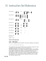
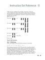
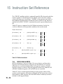
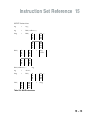
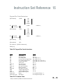
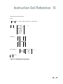
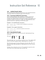
15 Instruction Set Reference
Multifunction Instructions
<ALU>*† ,
<MAC>*†
AX0
AX1
MX0
MX1
AX0
AX1
MX0
MX1
= DM (
<ALU>*
<MAC>*
<SHIFT>*
= DM (
I0
I1
I2
I3
, dreg
,
,
,
,
=
I0
I1
I2
I3
,
,
,
,
M0 ) ,
M1
M2
M3
DM (
PM (
DM (
PM (
<ALU>*
<MAC>*
<SHIFT>*
I0
I1
I2
I3
,
,
,
,
M0
M1
M2
M3
I4
I5
I6
I7
,
,
,
,
M4
M5
M6
M7
I4
I5
I6
I7
,
,
,
,
M4
M5
M6
M7
, dreg
=
)
= dreg,
M0 ) ,
M1
M2
M3
AY0
AY1
MY0
MY1
AY0
AY1
MY0
MY1
= PM (
= PM (
I0
I1
I2
I3
,
,
,
,
M0
M1
M2
M3
I4
I5
I6
I7
,
,
,
,
M4
M5
M6
M7
I4
I5
I6
I7
,
,
,
,
M4
M5
M6
M7
I4
I5
I6
I7
)
15 –8
;
)
<ALU>*
<MAC>*
<SHIFT>*
)
dreg;
Table 15.2 Multifunction Instructions
<ALU>
<MAC>
<SHIFT>
,
,
,
,
Any ALU instruction (except DIVS, DIVQ)
Any multiply/accumulate instruction
Any shifter instruction (except Shift Immediate)
* May not be conditional instruction
† AR, MR result registers must be used—not AF, MF feedback registers.
(See Section 15.4.1, “ALU/MAC with Data & Program Memory Read.”)
;
I4
I5
I6
I7
,
,
,
,
M4 );
M5
M6
M7
M4 );
M5
M6
M7
Instruction Set Reference 15
15.5
ALU, MAC & SHIFTER INSTRUCTIONS
This group of instructions performs computations. All of these
instructions can be executed conditionally except the ALU division
instructions and the Shifter SHIFT IMMEDIATE instructions.
15.5.1
ALU Group
Here is an example of one ALU instruction, Add/Add with Carry:
IF AC AR=AX0+AY0+C;
The (optional) conditional expression, IF AC, tests the ALU Carry bit
(AC); if there is a carry from the previous instruction, this instruction
executes, otherwise a NOP occurs and execution continues with the next
instruction. The algebraic expression AR=AX0+AY0+C means that the
ALU result register (AR) gets the value of the ALU X input and Y input
registers plus the value of the carry-in bit.
Table 15.3 gives a summary list of all ALU instructions. In this list,
condition stands for all the possible conditions that can be tested and xop
and yop stand for the registers that can be specified as input for the ALU.
The conditional clause is optional and is enclosed in square brackets to
show this. A complete list of the permissible xops and yops is given in the
reference page for each instruction. A complete list of conditions is given
in Table 15.9.
ALU Instructions
[IF condition]
AR
AF
=
xop
+ yop
+C
+ yop + C
+ constant
+ constant + C
;
[IF condition]
AR
AF
=
xop
– yop
– yop + C – 1
+C–1
– constant
– constant + C – 1
;
[IF condition]
AR
AF
=
yop
– xop
– xop + C – 1
– xop + C – 1
– xop + constant
– xop + constant + C – 1
;
15 – 9
15 Instruction Set Reference
[IF condition]
AR
AF
=
xop
AND
OR
XOR
yop
constant
[IF condition]
AR
AF
=
TSTBIT n OF xop
SETBIT n OF xop
CLRBIT n OF xop
TGLBIT n OF xop
;
[IF condition]
AR
AF
=
PASS
;
[IF condition]
AR
AF
=
–
xop
yop
;
[IF condition]
AR
AF
=
NOT
xop
yop
;
[IF condition]
AR
AF
=
ABS
xop
;
[IF condition]
AR
AF
=
yop
+1
;
[IF condition]
AR
AF
=
yop
–1
;
xop
yop
constant
;
DIVS yop, xop ;
DIVQ xop ;
NONE = <ALU> ;
Table 15.3 ALU Instructions
15.5.2
MAC Group
Here is an example of one of the MAC instructions, Multiply/Accumulate:
IF NOT MV MR=MR+MX0*MY0(UU);
The conditional expression, IF NOT MV, tests the MAC overflow bit. If the
condition is not true, a NOP is executed. The expression
MR=MR+MX0*MY0 is the multiply/accumulate operation: the multiplier
result register (MR) gets the value of itself plus the product of the X and Y
input registers selected. The modifier in parentheses (UU) treats the
operands as unsigned. There can be only one such modifier selected from
the available set. (SS) means both are signed, while (US) and (SU) mean
that either the first or second operand is signed; (RND) means to round
the (implicitly signed) result.
15 –10
Instruction Set Reference 15
Table 15.4 gives a summary list of all MAC instructions. In this list,
condition stands for all the possible conditions that can be tested and xop
and yop stand for the registers that can be specified as input for the MAC.
A complete list of the permissible xops and yops is given in the reference
page for each instruction.
MAC Instructions
[IF condition]
MR
MF
=
xop *
yop
xop
(
SS
SU
US
UU
RND
);
[IF condition]
MR
MF
=
MR + xop *
yop
xop
(
SS
SU
US
UU
RND
);
[IF condition]
MR
MF
=
MR – xop * yop
xop
(
SS
SU
US
UU
RND
);
[IF condition]
MR
MF
=
0;
[IF condition]
MR
MF
=
MR [( RND )];
IF MV SAT MR ;
Table 15.4 MAC Instructions
15.5.3
Shifter Group
Here is an example of one of the Shifter instructions, Normalize:
IF NOT CE SR= SR OR NORM SI (HI);
The conditional expression, IF NOT CE, tests the “not counter expired”
condition. If the condition is false, a NOP is executed. The destination of
all shifting operations is the Shifter Result register, SR. (The destination of
exponent detection instructions is SE or SB, as shown below.) In this
example, SI, the Shifter Input register, is the operand. The amount and
direction of the shift is controlled by the signed value in the SE register in
all shift operations except an immediate shift. Positive values cause left
shifts; negative values cause right shifts.
15 – 11
15 Instruction Set Reference
The “SR OR” modifier (which is optional) logically ORs the result with the
current contents of the SR register; this allows you to construct a 32-bit
value in SR from two 16-bit pieces. “NORM” is the operator and “(HI)” is
the modifier that determines whether the shift is relative to the HI or LO
(16-bit) half of SR. If “SR OR” is omitted, the result is passed directly into
SR.
Table 15.5 gives a summary list of all Shifter instructions. In this list,
condition stands for all the possible conditions that can be tested.
Shifter Instructions
[IF condition]
SR
=
[SR OR] ASHIFT xop
(
HI
LO
);
[IF condition]
SR
=
[SR OR] LSHIFT xop
(
HI
LO
);
[IF condition]
SR
=
[SR OR] NORM xop
(
HI
LO
);
[IF condition]
SE
=
EXP xop
(
HI
LO
HIX
);
[IF condition]
SB
=
EXPADJ xop;
SR
=
[SR OR] ASHIFT xop BY <exp>
(
HI
LO
);
SR
=
[SR OR] LSHIFT xop BY <exp>
(
HI
LO
);
Table 15.5 Shifter Instructions
15.6
MOVE: READ & WRITE
MOVE instructions, shown in Table 15.6, move data to and from data
registers and external memory. Registers are divided into two groups,
referred to as reg which includes almost all registers and dreg, or data
registers, which is a subset. Only the program counter (PC) and the ALU
and MAC feedback registers (AF and MF) are not accessible.
Table 15.7 shows which registers belong to these groups. Many of the
system control registers are memory-mapped (for the processors with onchip memory); these registers are read and written as memory locations
instead of with register names.
15 –12
Instruction Set Reference 15
MOVE Instructions
reg
=
reg ;
reg
=
DM (<address>) ;
dreg
=
DM (
DM (
I0
I1
I2
I3
,
,
,
,
M0
M1
M2
M3
I4
I5
I6
I7
,
,
,
,
M4
M5
M6
M7
DM (<address>) =
I0
I1
I2
I3
,
,
,
,
M0
M1
M2
M3
);
I4
I5
I6
I7
,
,
,
,
M4
M5
M6
M7
)
=
dreg
<data>
I4
I5
I6
I7
,
,
,
,
M4
M5
M6
M7
)
=
dreg;
;
reg;
reg
=
<data> ;
dreg
=
PM (
PM (
I4
I5
I6
I7
,
,
,
,
M4
M5
M6
M7
);
Table 15.6 MOVE Instructions
15 – 13
15 Instruction Set Reference
Registers: reg
SB
PX
I0 – I7, M0 – M7, L0 – L7
CNTR
ASTAT, MSTAT, SSTAT
IMASK, ICNTL, IFC
TX0, TX1, RX0, RX1
Data Registers: dreg
AX0, AX1, AY0, AY1, AR
MX0, MX1, MY0, MY1, MR0, MR1, MR2
SI, SE, SR0, SR1
Table 15.7 Processor Registers: reg & dreg
15.7
PROGRAM FLOW CONTROL
Program flow control on the ADSP-2100 family processors is simple but
powerful. Here is an example of one instruction:
IF EQ JUMP my_label;
JUMP, of course, is a familiar construct from many other languages. My_label
is any identifier you wish to use as a label for the destination jumped to.
Instead of the label, an index register in DAG2 may be explicitly used. The
default scope for any label is the source code module in which it is declared.
The assembler directive .ENTRY makes a label visible as an entry point for
routines outside the module. Conversely, the .EXTERNAL directive makes it
possible to use a label declared in another module.
If the counter condition (CE, NOT CE) is to be used, an assignment to CNTR
must be executed to initialize the counter value. JUMP and CALL permit the
additional conditionals “FLAG_IN” and “NOT FLAG_IN” to be used for
branching on the state of the FI pin, but only with direct addressing, not with
DAG2 as the address source.
RTS (return from subroutine) and RTI (return from interrupt) provide for
conditional return from CALL or interrupt vectors respectively.
The IDLE instruction provides a way to wait for interrupts. IDLE causes the
processor to wait in a low-power state until an interrupt occurs. When an
interrupt is serviced, control returns to the instruction following the IDLE
statement. IDLE uses less power than loops created with JUMP.
Table 15.8 gives a summary of all program flow control instructions. The
condition codes are described in Table 15.9.
15 –14
Instruction Set Reference 15
Program Flow Control Instructions
[IF condition]
IF
FLAG_IN
NOT FLAG_IN
[IF condition]
IF
JUMP
CALL
FLAG_IN
NOT FLAG_IN
[IF condition]
RTS ;
[IF condition]
RTI ;
(I4)
(I5)
(I6)
(I7)
<address>
;
JUMP
(I4)
(I5)
(I6)
(I7)
<address>
CALL
<address> ;
;
<address> ;
DO <address> [UNTIL termination] ;
IDLE [(n)];
Table 15.8 Program Flow Control Instructions
Syntax
EQ
NE
LT
GE
LE
GT
AC
NOT AC
AV
NOT AV
MV
NOT MV
NEG
POS
NOT CE
FLAG_IN*
NOT FLAG_IN*
Status Condition
Equal Zero
Not Equal Zero
Less Than Zero
Greater Than or Equal Zero
Less Than or Equal Zero
Greater Than Zero
ALU Carry
Not ALU Carry
ALU Overflow
Not ALU Overflow
MAC Overflow
Not MAC Overflow
X Input Sign Negative
X Input Sign Positive
Not Counter Expired
FI pin
Not FI pin
True If:
AZ = 1
AZ = 0
AN .XOR. AV = 1
AN .XOR. AV = 0
(AN .XOR. AV) .OR. AZ = 1
(AN .XOR. AV) .OR. AZ = 0
AC = 1
AC = 0
AV = 1
AV = 0
MV = 1
MV = 0
AS = 1
AS = 0
Last sample of FI pin = 1
Last sample of FI pin = 0
Table 15.9 IF Condition Codes
* Only available on JUMP and CALL instructions
15 – 15
15 Instruction Set Reference
15.8
MISCELLANEOUS INSTRUCTIONS
There are several miscellaneous instructions. NOP is a no operation
instruction. The PUSH/POP instructions allows you to explicitly control
the status, counter, PC and loop stacks; interrupt servicing automatically
pushes and pops some of these stacks.
The Mode Control instruction enables and disables processor modes of
operation: bit-reversal on DAG1, latching ALU overflow, saturating the
ALU result register, choosing the primary or secondary register set, GO
mode for continued operation during bus grant, multiplier shift mode for
fractional or integer arithmetic, and timer enabling.
A single ENA or DIS can be followed by any number of mode identifiers,
separated by commas; ENA and DIS can also be repeated. All seven
modes can be enabled, disabled, or changed in a single instruction.
The MODIFY instruction modifies the address pointer in the I register
selected with the value in the selected M register, without performing any
actual memory access. As always, the I and M registers must be from the
same DAG; any of I0-I3 may be used only with one from M0-M3 and the
same for I4-I7 and M4-M7. If circular buffering is in use, modulus logic
applies (See Chapter 4, “Data Transfer,” for more information).
The FO (Flag Out), FL0, FL1 and FL2 pins can each be set, cleared, or
toggled. This instruction provides a control structure for multiprocessor
communication.
15 –16
Instruction Set Reference 15
Miscellaneous Instructions
NOP;
[ PUSH ] STS
POP
ENA
DIS
BIT_REV
AV_LATCH
AR_SAT
SEC_REG
G_MODE
M_MODE
TIMER
MODIFY (
[IF condition]
ENA
DIS
[, POP CNTR] [, POP PC] [, POP LOOP] ;
[,]
I0
I1
I2
I3
,
,
,
,
M0
M1
M2
M3
I4
I5
I6
I7
,
,
,
,
M4
M5
M6
M7
SET
RESET
TOGGLE
;
);
FLAG_OUT
FL0
FL1
FL2
[,]
;
INTS ;
Table 15.10 Miscellaneous Instructions
15 – 17
15 Instruction Set Reference
15.9
EXTRA CYCLE CONDITIONS
All instructions execute in a single cycle except under certain conditions,
as explained below.
15.9.1
Multiple Off-Chip Memory Accesses
The data and address busses of the ADSP-21xx processors are multiplexed
off-chip. Because of this, the processors can perform only one off-chip
access per instruction in a single cycle. If two off-chip accesses are
required—the instruction fetch and one data fetch, for example, or data
fetches from both program and data memory—then one overhead cycle
occurs. In this case the program memory access occurs first, then the data
memory access. If three off-chip accesses are required—the instruction
fetch as well as data fetches from both program and data memory—then
two overhead cycles occur.
A multifunction instruction requires three items to be fetched from
memory: the instruction itself and two data words. No extra cycle is
needed to execute the instruction as long as only one of the fetches is from
external memory. (Two fetches must be from on-chip memory, either PM
or DM.)
15.9.2
Wait States
All family processors allow the programming of wait states for external
memory chips. Up to seven extra wait state cycles may be added to the
processor’s access time for external memory. Extra cycles inserted due to
wait states are in addition to any caused by multiple off-chip accesses (as
described above). Wait state programming is described in the “Memory
Interface” chapter.
Wait states and multiple off-chip memory accesses are the two cases when
an extra cycle is generated during instruction execution. The following
case, SPORT autobuffering and DMA, causes the insertion of extra cycles
between instructions.
15.9.3
SPORT Autobuffering & DMA
If serial port autobuffering or ADSP-2181 DMA is being used to transfer
data words to or from internal memory, then one memory access is
“stolen” for each transfer. The stolen memory access occurs only between
complete instructions. If extra cycles are required to execute any
instruction (for one of the two reasons above), the processor waits until it
is completed before “stealing” the access cycle.
15 –18
Instruction Set Reference 15
15.10
INSTRUCTION SET SYNTAX
The following sections describe instruction set syntax and other notation
conventions used in the reference page of each instruction.
15.10.1 Punctuation & Multifunction Instructions
All instructions terminate with a semicolon. A comma separates the
clauses of a multifunction instruction but does not terminate it. For
example, the statements below in Example A comprise one multifunction
instruction (which can execute in a single cycle). Example B shows two
separate instructions, requiring two instruction cycles.
Example A: One multifunction instruction
AX0 = DM(I0, M0), a comma is used in multifunction instructions
AY0 = PM(I4, M4);
Example B: Two separate instructions
AX0 = DM(I0, M0); a semicolon terminates an instruction
AY0 = PM(I4, M4);
15.10.2 Syntax Notation Example
Here is an example of one instruction, the ALU Add/Add with Carry
instruction:
[ IF cond ]
AR = xop +
AF
yop
C
yop + C
;
The permissible conds, xops and yops are given in a list. The conditional IF
clause is enclosed in square brackets, indicating that it is optional.
The destination register for the add operation must be either AR or AF.
These are listed within parallel bars, indicating that one of the two must
be chosen.
Similarly, the yop term may consist of a Y operand, the carry bit, or the
sum of both. One of these three terms must be used.
15 – 19
15 Instruction Set Reference
15.10.3 Status Register Notation
The following notation is used in the discussion of the effect each
instruction has on the processors’ status registers:
*
An asterisk indicates a bit in the status word that is changed by
the execution of the instruction.
–
A dash indicates that a bit is not affected by the instruction.
0 or 1
Indicates that a bit is unconditionally cleared or set.
For example, the status word ASTAT is shown below:
ASTAT:
7
SS
–
6
5
4
MV AQ AS
*
–
–
3
AC
–
2
AV
0
1
0
AN AZ
–
–
Here the MV bit is updated and the AV bit is cleared.
15 –20