1
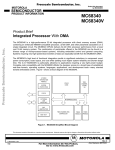
Freescale Semiconductor, Inc.
Product Brief
MCF5206EPB/D
Rev. 2.1, 3/2002
Freescale Semiconductor, Inc...
MCF5206e Integrated
ColdFire® Microprocessor
Product Brief
The MCF5206e integrated microprocessor combines a ColdFire® core with several peripheral
functions such as a DRAM controller, timers, parallel and serial interfaces, and system
integration. This device is an enhanced version of the MCF5206, which is in production today.
Not only does the MCF5206e provide a performance upgrade to the MCF5206 due to the
increased 4-Kbyte I-cache, 8-Kbyte SRAM and increased frequency, but this device also
integrates an additional multiply accumulate (MAC) unit, hardware divide, and two-channel
DMA to the device while maintaining pin compatibility with the MCF5206.
The revolutionary ColdFire architecture gives cost-sensitive, high-volume markets new levels
of price and performance. Based upon the concept of variable-length RISC technology, the
ColdFire core combines the architectural simplicity of conventional 32-bit RISC with a
memory-saving, variable-length instruction set. In defining the ColdFire architecture for
embedded processing applications, Motorola incorporated RISC architecture for peak
performance and a simplified version of the variable-length instruction set found in the
M68000 family for code density.
By using a variable-length instruction set architecture, embedded processor designers using
ColdFire processors will enjoy significant system-level advantages over conventional
fixed-length RISC architectures. The denser binary code for ColdFire uses less memory than
fixed-length instruction processors available. This improved code density means more
efficient system memory usage for a given application, and allows for slower, less costly
memory to help achieve a target price/performance level for embedded processing
applications.
The MCF5206e Version 2 core delivers enhanced performance while maintaining low system
costs. The addition of a MAC module and hardware divide to the core increases performance
of complex arithmetic functions normally used in DSP applications. To speed program
execution, the on chip instruction cache and SRAM provides one-cycle access to critical code
and data. The MCF5206e processor greatly reduces the time required for system design and
implementation by packaging common system functions on chip and providing glueless
interfaces to 8 bit, 16 bit and 32 bit DRAM, SRAM, ROM and I/O devices.
The integrated peripheral functions provide high performance and flexibility. The DRAM
controller supports up to 512 Mbytes of DRAM. The MCF5206e processor supports both fast
page-mode and extended-data-out DRAMs. The DMA controller provides two fully
programmable channels that support both single and dual addressing modes. The serial
interfaces consists of two independent UARTs and a separate I2C-compatible1 Motorola bus
(M-Bus interface). Two 16-bit general-purpose multimode timers provide separate input and
output signals. For system protection, the processor includes a programmable 16-bit software
For More Information On This Product,
Go to: www.freescale.com
Freescale Semiconductor, Inc.
MCF5206e Overview
watchdog timer and several bus monitors. In addition, common system functions such as chip-selects,
interrupt control, bus arbitration and IEEE 1149.1 Test (JTAG) support are included.
A sophisticated debug interface supports both background-debug mode and real-time trace. The interface is
common to all ColdFire-based processors and allows emulator support across the entire ColdFire family.
1.1
MCF5206e Overview
This section gives a brief overview of the MCF5206e processor. Figure 1 is a block diagram of the
MCF5206e processor.
Clock
Input
Clock
JTAG
Interface
JTAG
System Bus
Controller
Freescale Semiconductor, Inc...
.
4KByte
ICache
DRAM
Controller
DRAM
Control
Chip
Selects
Chip
Selects
Interrupt
Controller
Interrupt
Support
External
Bus
Interface
External
Bus
Parallel
Port
8KByte
SRAM
BOM
Interface
Parallel
Interface
DUART
Serial
Interface
Timers
Timer
Support
M-Bus
Module
M-Bus
Interface
H/W Divide
Coldfire
Core
MAC
Debug Module
DMA
Controller
DMA
Control
Figure 1. MCF5206e Block Diagram
1.1.1
Features List
The following are the primary features of the MCF5206e integrated processor:
•
ColdFire Version 2 core
— Variable-length RISC
— 32-bit internal address bus with 28-bit external bus; chip select and DRAM decoding use
internal 32 bit
— 32-bit data base
2
MCF5206e Integrated ColdFire® Microprocessor Product Brief
For More Information On This Product,
Go to: www.freescale.com
MOTOROLA
Freescale Semiconductor, Inc.
MCF5206e Overview
— 16 user-visible 32-bit wide registers
— Supervisor and user modes for system protection
— Vector base register to relocate exception-vector table
— Optimized for high level language constructs
— 50 MIPS at 54 MHz
•
Multiply accumulate
— High speed, complex arithmetic functions for signal processing applications
— Single clock issue rate with 3-stage execution pipeline
— One MAC cycle for 16x16 and 32x32 multiplies, all with 32-bit accumulate
Freescale Semiconductor, Inc...
— Four-Kbyte direct-mapped instruction cache
— Eight-Kbyte on-chip SRAM that provides one-cycle access to critical code and data
•
DRAM controller
— Programmable refresh timer provides CAS before RAS refresh
— Support for 2 separate memory banks
— Support for fast page mode DRAMs and extended-data-out (EDO) DRAMs
— External bus master access
•
DMA controller
— Two fully programmable channels with external request pins supporting dual-address and
single address transfers with 32-bit capability
— Two address pointers per channel that can increment or remain constant
— 16-bit transfer counter per channel
— Operand packing and unpacking
— Auto-alignment transfers for efficient block movement
— Bursting and cycle stealing
— Two clock-cycle internal access
•
Two universal synchronous/asynchronous receiver/transmitters (UARTs)
— Full duplex operation
— Baud-rate generator
— Modem control signals (CTS, RTS)
— Processor-interrupt capability
•
Dual 16-bit general-purpose multimode timers
— 8-bit prescaler
— Timer input and output pins
— 12 ns resolution with 54 MHz system clock
— Processor interrupt capability
•
Motorola bus (M-Bus) module
— Interchip bus interface for EEPROMs, LCD controllers, A/D converters, keypads
— Compatible with industry-standard I2C bus
MOTOROLA
MCF5206e Integrated ColdFire® Microprocessor Product Brief
For More Information On This Product,
Go to: www.freescale.com
3
Freescale Semiconductor, Inc.
MCF5206e Overview
— Master or slave modes supporting multiple masters
— Automatic interrupt generation with programmable level
•
System interface
— Glueless bus interface to 8 bit, 16 bit, and 32 bit DRAM, SRAM, ROM, and I/O devices
— Eight programmable chip selects and programmable wait states and port sizes allowing
external bus masters to access chip selects
— Programmable external interrupts
— 8-bit general-purpose I/O interface
— System protection
– 16-bit software watchdog timer with prescaler
Freescale Semiconductor, Inc...
– Double bus fault monitor
– Bus timeout monitor
– Spurious interrupt monitor
– Programmable interrupt controller (low interrupt latency, 3 external interrupt inputs, and
programmable interrupt priority and autovector generator)
— IEEE 1149.1 test (JTAG) support
•
System debug interface
— Real-time trace
— Background debug mode (BDM)
•
Fully static 3.3-volt operation with 5-volt tolerant inputs
•
160-pin QFP package; pin-compatible with MCF5206
1.1.2
ColdFire Version 2 Core
The ColdFire processor core consists of two independent, decoupled pipeline structures that maximize
performance while minimizing core size. The instruction fetch pipeline (IFP) is a two-stage pipeline for
prefetching instructions. The prefetched instruction stream is then gated into the two-stage operand
execution pipeline (OEP), which decodes the instruction, fetches the required operands and then executes
the required function. The IFP and OEP pipelines are decoupled by an instruction buffer that serves as a
FIFO queue, the IFP can prefetch instructions in advance of their actual use by the OEP, thereby minimizing
time stalled waiting for instructions. The OEP is implemented in a two-stage pipeline featuring a traditional
RISC datapath with a dual-read-ported register file feeding an arithmetic/logic unit.
1.1.3
Instruction Cache
The instruction cache improves system performance by providing cached instructions to the execution unit
in a single clock. The MCF5206e processor uses a 4-Kbyte, direct-mapped instruction cache to achieve 50
MIPS at 54 MHz. The cache is accessed by physical addresses, where each 16-byte line consists of an
address tag and a valid bit. The instruction cache also includes a bursting interface for 32-bit, 16-bit, and
8-bit port sizes to fill cache lines quickly.
4
MCF5206e Integrated ColdFire® Microprocessor Product Brief
For More Information On This Product,
Go to: www.freescale.com
MOTOROLA
Freescale Semiconductor, Inc.
MCF5206e Overview
1.1.4
Internal SRAM
The 8-Kbyte on-chip SRAM provides one clock-cycle access for the ColdFire core. The SRAM can store
processor stack and critical code or data segments to maximize performance.
1.1.5
DRAM Controller
Freescale Semiconductor, Inc...
The MCF5206e DRAM controller provides a glueless interface for up to 2 banks of DRAM, each of which
can range from 128 Kbytes to 256 Mbytes. The controller supports an 8-, 16-, or 32-bit data bus. A unique
addressing schemes allows for increases in system memory size without rerouting address lines and
rewiring boards. The controller operates in fast page or regular mode and supports extended-data-out (EDO)
DRAMs.
1.1.6
MAC Module
The MAC unit provides high performance digital signal processing capabilities for the MCF5206e.
Integrated as an execution unit in the processor’s operand execution pipeline, the MAC unit implements a
three-stage arithmetic pipeline with sustained instruction issue rate of one MAC cycle for 16x16 operations
(while also supporting 32x32 operations). The MAC opcodes provide a full feature set of extensions to the
standard ColdFire instruction set for signed and unsigned operands. In addition to executing the
MAC-specific instructions, this unit also performs all integer multiply opcodes, providing higher
performance for this class of operation.
1.1.7
DMA Controller
The MCF5206e provides two fully programmable DMA channels for quick data transfer (32 bits, with
packing and unpacking supported). Each channel has an external request pin associated with it. Single and
dual address mode is supported with the ability for program bursting and cycle stealing. With
auto-alignment enabled, efficient block transfers of up to 128 bits can be achieved.
1.1.8
Dual UART Modules
The UART modules contain independent receivers and transmitters that are clocked by the UART internal
timer. This timer is clocked by the system clock or an external clock supplied by the TIN pin. Data formats
can be 5, 6, 7 or 8 bits with even, odd, or no parity, and as many as two stop bits in 1/16 increments.
Four-byte receive buffers and 2-byte transmit buffers minimize CPU service calls. The UART modules also
provide several error-detection and maskable-interrupt capabilities. Modem support includes
request-to-send (RTS) and clear-to-send (CTS) signals.
The system clock provides the clocking function via a programmable prescaler. Select full duplex, autoecho
loopback, local loopback, and remote loopback modes. The programmable UARTs can interrupt the CPU
on various normal or error condition events.
1.1.9
Dual Timer Module
The timer module includes two general-purpose timers, each of which contains a free-running 16-bit timer
for use in any of the three modes. One mode captures the timer value with an external event; another mode
triggers an external signal or interrupts the CPU when the timer reaches a set value, while a third mode
counts external events. The timer unit has an 8-bit prescaler that allows programming of the clock input
MOTOROLA
MCF5206e Integrated ColdFire® Microprocessor Product Brief
For More Information On This Product,
Go to: www.freescale.com
5
Freescale Semiconductor, Inc.
MCF5206e Overview
frequency, which is derived from the system clock. The programmable timer-output pin generates either an
active low-pulse or toggles the output.
1.1.10 Motorola Bus (M-Bus) Module
The M-Bus interface is a two-wire, bidirectional serial bus that exchanges data between devices and is
compatible with the I2C bus standard. The M-Bus minimizes the interconnection between devices in the end
system and is best suited for applications that need occasional bursts of rapid communication over short
distances among several devices. Bus capacitance and the number of unique addresses limit the maximum
communication length and the number of devices that can be connected.
Freescale Semiconductor, Inc...
1.1.11 System Interface
The MCF5206e processor provides a glueless interface to 8-, 16-, and 32-bit port size SRAM, ROM, and
peripheral devices with independent programmable control of the assertion and negation of chip-selects and
write-enables. Programmable address and data-hold times can be extended for a compatible interface to
external devices and memory. The MCF5206e also supports bursting ROMs.
1.1.11.1 External Bus Interface
The bus interface controller transfers information between the ColdFire core and memory, peripherals, or
other masters on the external bus. The external bus interface provides as much as 28 bits of address bus
space, a 32-bit data bus, and all associated control signals. This interface implements an extended
synchronous protocol that supports bursting operations. For nonsynchronous external memory and
peripherals, the MCF5206e processor provides an alternate asynchronous bus transfer acknowledgment
signal.
Simple two-wire request/acknowledge bus arbitration between the MCF5206e processor and another bus
master, such as the DMA device, is glueless with arbitration handled internal to the MCF5206e processor.
Alternately, an external bus arbiter can control more complex three-wire (request, grant, busy)
multiple-master bus arbitration, allowing overlapped bus arbitration with one clock-bus handovers.
1.1.11.2 Chip Selects
Eight programmable chip select outputs provide signals that enable external memory and peripheral circuits
for automatic wait-state insertion. These signals also interface to 8-, 16-, 32-bit ports. In addition, other
external bus masters can access chip selects. The other four chip-selects are multiplexed with A[27:24] of
the address bus and four write-enable signals. The base address, access permissions, and timing waveforms
are all programmable using configuration registers.
Except for fast page mode, all operations are available to other external bus masters. The DRAM controller
can generate RAS and CAS for an external master and can continue to generate refresh requests.
1.1.11.3 8-Bit Parallel Port Interface
An 8-bit general-purpose programmable parallel port serves as either an input or output on a bit-by-bit basis.
The parallel port is multiplexed with the PST[3:0] and DDATA[3:0] debug signals.
6
MCF5206e Integrated ColdFire® Microprocessor Product Brief
For More Information On This Product,
Go to: www.freescale.com
MOTOROLA
Freescale Semiconductor, Inc.
MCF5206e Overview
1.1.11.4 Interrupt Controller
The interrupt controller provides user-programmable control of 3 or 7 external interrupt to any one of 7
interrupt levels and 4 priority levels. The 3 external interrupt signals can be configured as either fixed
interrupt levels 1, 4, and 7, or as a 7-level encoded interrupt. The external interrupts can also be programmed
to any one of the four priority levels within the respective interrupt levels.
1.1.11.5 System Protection
Freescale Semiconductor, Inc...
The MCF5206e processor contains a 16-bit software watchdog timer with an 8-bit prescaler. The
programmable software watchdog timer provides either a level 7 interrupt or a hardware reset on timeout.
The MCF5206e processor also contains a reset status register that indicates the cause of the last reset.
1.1.11.6 JTAG
To help with system diagnostics and testing during manufacture, the MCF5206e processor includes
dedicated user-accessible test logic that complies with the IEEE 1149.1 standard for boundary scan
testability, often referred to as Joint Test Action Group, or JTAG. For more information, refer to the IEEE
1149.1 standard.
1.1.12 System Debug Interface
The ColdFire interface supports real-time trace and background debug mode. A 4-pin background debug
mode (BDM) interface provides system debug. The BDM is a superset of the BDM interface provided on
Motorola’s 683xxx family of parts.
In real-time trace, 4 status lines provide information on processor activity in real time (PST pins). A 4-bit
wide debug data bus (DDATA) displays operand data, which helps track the machine’s dynamic execution
path as the change-of-flow instructions execute. These signals are multiplexed with the 8-bit parallel port
for application development which does not use real-time trace.
1.1.13 System Diagrams
This section includes system and pinout diagrams. Figure 2 shows the system of the MCF5206e device.
MOTOROLA
MCF5206e Integrated ColdFire® Microprocessor Product Brief
For More Information On This Product,
Go to: www.freescale.com
7
Freescale Semiconductor, Inc.
MCF5206e Overview
TS
STA
ATA
TEA
TT[1:0]
ATM
SIZ[1:0]
R/W
MTMOD
TCK
TDO/DSO
TMS/BKPT
TSI/DSI
TRST/DSCLK
HIZ
RSTI
BD
JTAG
Port
Parallel
I/O Port
PP[7:0]
PST[3:0]
DDATA[3:0]
Debug Module
Bus
Interface
D[31:0]
Coldfire
Core
MAC
H/W Divide
4 Kbyte
Instruction
Cache
8 Kbyte
SRAM
A[23:0]
A[27:24]/
WE[3:0]/
CS[7:4]
Chip Selects
System Bus
Controller
CS[3:0]
Interrupt
Controller
Clock
DUART
Serial I/O
Dual
DMA
Timer Controller
Module
TOUT[1:0]/DREQ1
DRAMW
M-Bus
(I2C]
Module
TIN[1:0]/DREQ0
CAS[3:0]
DRAM
Controller
SDA
TXD1
RXD1
RTS1
CTS1
TXD2
RXD2
RTS2/RSTO
CTS2
RAS[1:0]
SCL
IRQ7 / IPL2
IRQ4 / IPL1
IRQ1 / IPL0
CLK
Freescale Semiconductor, Inc...
BR
BG
.
Figure 2. MCF5206e System Diagram
8
MCF5206e Integrated ColdFire® Microprocessor Product Brief
For More Information On This Product,
Go to: www.freescale.com
MOTOROLA
Freescale Semiconductor, Inc.
MCF5206e Overview
Figure 3 shows the MCF5206e pinout that is supplied in a 160-pin plastic quad flat pack.
MCF5206e
Top View
D30
D31
DRAMW
VDD
CAS3
CAS2
CAS1
GND
CAS0
RAS1
RAS0
VDD
BG
BD
BR
GND
IRQ1/IPL0
IRQ4/IPL
IRQ7/IPL2
ATA
VDD
RST
TS
TEA
GND
TA
R/W
SIZ1
VDD
SIZ0
ATM
TT1
GND
TT0
CS3
CS2
VDD
CS1
CS0
A27/CS7/WE0
160
1
A26/CS6/WE11
GND
AA25/CS6/CS5/WE
A24/CS4/WE31
VDD
A23
A22
GND
A21
A2O
VDD
A19
A18
VSS
A17
A16
VDD
A15
A14
GND
A13
A12
VDD
A11
A10
GND
A9
A8
VDD
A7
A6
GND
A5
A4
VDD
A3
A2
GND
A1
A0
Freescale Semiconductor, Inc...
D29
GND
D28
D27
D26
VDD
D25
D24
D23
GND
D22
D21
D20
VDD
D19
D18
D17
GND
D16
D15
D14
VDD
D13
D12
D11
GND
D10
D9
D8
VDD
D7
D6
D5
GND
D4
D3
D2
VDD
D1
D0
TRST/DSCLK
TCK
GND
TDO/DSO
HIZ
TDI/DSL
TMS/BKPI
VDD
JTAG
GND
GND
CTS2
RTS2/RTSO
GND
CLK
RXD2
TXD2
CTS1
RTS1
VDD
RXD1
TXD1
DREQ0/TIN0
TIN1
GND
DREQ1/TOUI0
TOUT1
SDA
SCL
VDD
PP7/PST3
PP6/PST2
PP5/PST1
PP4/PST0
GND
PP3/DDATA3
PP2/DDATA2
PP1/DDATA1
PPO/DDATA0
VDD
Figure 3. MCF5206e Pinout Diagram
MOTOROLA
MCF5206e Integrated ColdFire® Microprocessor Product Brief
For More Information On This Product,
Go to: www.freescale.com
9
Freescale Semiconductor, Inc.
MCF5206e Overview
1.1.14 QFP Packages and Operating Frequencies
Table 1 identifies the packages and operating frequencies available for the MCF5206e processor.
Table 1. MCF5206e Package/Frequency Availability
Package
Frequency
Temperature
Plastic Quad Flat Pack 160 lead
40, and 54 MHz
0 to 70 C
Plastic Quad Flat Pack 160 lead
40 MHz
-40 to +85 C
1.1.15 Document Availability
Freescale Semiconductor, Inc...
Table 2 provides information on documentation available for the MCF5206e microprocessor.
Table 2. Document Availability
Document Order Number
Document Title
MCF5206EPB/D
MCF5206e Integrated Microprocessor Product Brief
MCF5206EUM/D
MCF5206e User’s Manual
CFPRM/D
ColdFire Family Programmer’s Reference Manual
1.1.16 Development Tools
Development tools for the MCF5206e processor consist of a complete suite of compilers and debuggers
available from third-party developers, as shown in Table 3. Any development tool that generates code for
the Motorola ColdFire MCF5206 can do the same for the MCF5206e processor.
Table 3. Development Tools
Company Name
Company Phone Number
Availability
Compliers/Debuggers
Diab Data
415-571-1700
Now
Software Development Systems
708-368-0400
Now
RTOS
Integrated Systems
408-542-1781
Now
Embeded System Product
617-828-5588
Now
Wind River Systems
510-748-5588
Now
Emulators
10
Yokogawa/Orion Instruments
408-747-0440
Now
Embeded Support Tools (EST)
617-828-5588
Now
Noral Micrologics
508-647-1013
Lauterbach
508-620-4521
Now
Microtek
503-645-7333
Now
MCF5206e Integrated ColdFire® Microprocessor Product Brief
For More Information On This Product,
Go to: www.freescale.com
MOTOROLA
Freescale Semiconductor, Inc.
MCF5206e Overview
Table 3. Development Tools (continued)
Company Name
Company Phone Number
Availability
Logic Analyzers
Hewlett-Packard (preprocessors only)
719-590-2558
Now
Development Boards
Order Number
M5206 eAN
—
Now
Freescale Semiconductor, Inc...
1.1.17 Revision History
Table 4. Revision History
Revision
Date
Rev 1
1998
Rev 2
1/2002
New product brief format.
Rev 2.1
3/2002
In the system diagram on page 8:
Added MTMOD signal to JTAG block.
Corrected signal direction arrow on ATM pin to indicate output.
Corrected signal direction arrow on CS[7:4]/A[27:24]/WE[3:0] pins to
indicate input/output
Changed interrupt controller pins names to IRQ7/IPL2,IRQ4/IPL1,
IRQ1/IPL0.
Corrected signal direction arrow on TT[1:0] signals to indicate output.
Added Revision History section.
MOTOROLA
Changes
Initial Release
MCF5206e Integrated ColdFire® Microprocessor Product Brief
For More Information On This Product,
Go to: www.freescale.com
11
Freescale Semiconductor, Inc.
HOW TO REACH US:
USA/EUROPE/LOCATIONS NOT LISTED:
Motorola Literature Distribution
P.O. Box 5405, Denver, Colorado 80217
1-303-675-2140 or 1-800-441-2447
JAPAN:
Freescale Semiconductor, Inc...
Motorola Japan Ltd.
SPS, Technical Information Center
3-20-1, Minami-Azabu Minato-ku
Tokyo 106-8573 Japan
81-3-3440-3569
Information in this document is provided solely to enable system and software implementers to use
ASIA/PACIFIC:
Motorola products. There are no express or implied copyright licenses granted hereunder to design
Motorola Semiconductors H.K. Ltd.
Silicon Harbour Centre, 2 Dai King Street
Tai Po Industrial Estate, Tai Po, N.T., Hong Kong
852-26668334
or fabricate any integrated circuits or integrated circuits based on the information in this document.
TECHNICAL INFORMATION CENTER:
use of any product or circuit, and specifically disclaims any and all liability, including without
1-800-521-6274
limitation consequential or incidental damages. “Typical” parameters which may be provided in
HOME PAGE:
Motorola reserves the right to make changes without further notice to any products herein.
Motorola makes no warranty, representation or guarantee regarding the suitability of its products
for any particular purpose, nor does Motorola assume any liability arising out of the application or
Motorola data sheets and/or specifications can and do vary in different applications and actual
performance may vary over time. All operating parameters, including “Typicals” must be validated
http://www.motorola.com/semiconductors
for each customer application by customer’s technical experts. Motorola does not convey any
DOCUMENT COMMENTS:
license under its patent rights nor the rights of others. Motorola products are not designed,
FAX (512) 933-2625
Attn: TECD Applications Engineering
intended, or authorized for use as components in systems intended for surgical implant into the
body, or other applications intended to support or sustain life, or for any other application in which
the failure of the Motorola product could create a situation where personal injury or death may
occur. Should Buyer purchase or use Motorola products for any such unintended or unauthorized
application, Buyer shall indemnify and hold Motorola and its officers, employees, subsidiaries,
affiliates, and distributors harmless against all claims, costs, damages, and expenses, and
reasonable attorney fees arising out of, directly or indirectly, any claim of personal injury or death
associated with such unintended or unauthorized use, even if such claim alleges that Motorola was
negligent regarding the design or manufacture of the part.
Motorola and the Stylized M Logo are registered in the U.S. Patent and Trademark Office.
digital dna is a trademark of Motorola, Inc. All other product or service names are the property of
their respective owners. Motorola, Inc. is an Equal Opportunity/Affirmative Action Employer.
© Motorola, Inc. 2002
MCF5206EPB/D
For More Information On This Product,
Go to: www.freescale.com