1
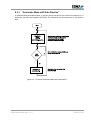
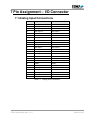
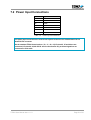
The Embedded I/O Company
TIP500
Optically Isolated 16 Channel 12 Bit ADC
Version 1.1
User Manual
Issue 1.1.9
January 2010
TEWS TECHNOLOGIES GmbH
Am Bahnhof 7 25469 Halstenbek, Germany
Phone: +49 (0) 4101 4058 0 Fax: +49 (0) 4101 4058 19
e-mail: [email protected] www.tews.com
TIP500-10
Optically isolated 16 channel 12 bit ADC input
voltage range +/-10V, gain 1, 2, 5, 10
TIP500-11
Optically isolated 16 channel 12 bit ADC input
voltage range +/-10V, gain 1, 2, 4, 8
TIP500-20
Optically isolated 16 channel 12 bit ADC input
voltage range 0V to +10V, gain 1, 2, 5, 10
TIP500-21
Optically isolated 16 channel 12 bit ADC input
voltage range 0V to +10V, gain 1, 2, 4, 8
This document contains information, which is
proprietary to TEWS TECHNOLOGIES GmbH. Any
reproduction without written permission is forbidden.
TEWS TECHNOLOGIES GmbH has made any
effort to ensure that this manual is accurate and
complete. However TEWS TECHNOLOGIES GmbH
reserves the right to change the product described
in this document at any time without notice.
TEWS TECHNOLOGIES GmbH is not liable for any
damage arising out of the application or use of the
device described herein.
Style Conventions
Hexadecimal characters are specified with prefix 0x,
i.e. 0x029E (that means hexadecimal value 029E).
For signals on hardware products, an ‚Active Low’ is
represented by the signal name with # following, i.e.
IP_RESET#.
Access terms are described as:
W
Write Only
R
Read Only
R/W
Read/Write
R/C
Read/Clear
R/S
Read/Set
©1996-2010 by TEWS TECHNOLOGIES GmbH
All trademarks mentioned are property of their respective owners.
TIP500 User Manual Issue 1.1.9
Page 2 of 26
Issue
Description
Date
1.0
First Issue
February 1996
1.1
Technical Specification
April 1996
1.2
Data Correction
April 1999
1.3
General Revision
September 2002
1.4
Technical Specification and Flowcharts
November 2002
1.5
Added Programming Note and Installation Note
October 2004
1.6
Correction ADC Data Coding description
November 2004
1.7
New address TEWS LLC
September 2006
1.8
Special I/O pin connection clarified, new MTBF number
July 2007
1.1.9
New Notation for User Manual and Engineering Documentation,
Added Analog Input Impedance
January 2010
TIP500 User Manual Issue 1.1.9
Page 3 of 26
Table of Contents
1
2
3
PRODUCT DESCRIPTION ......................................................................................... 6
TECHNICAL SPECIFICATION................................................................................... 7
FUNCTIONAL DESCRIPTION ................................................................................... 8
3.1 Analog Input ....................................................................................................................................8
3.2 Data Correction ...............................................................................................................................9
3.2.1 ADC Correction Formula ......................................................................................................9
4
5
ID PROM CONTENT ................................................................................................ 10
IP ADDRESSING...................................................................................................... 11
5.1 ADC Register Set ..........................................................................................................................11
5.1.1 ADC Control Register (Address 0x00)................................................................................11
5.1.2 ADC Data Register (Address 0x02)....................................................................................13
5.1.3 ADC Status Register (Address 0x05) .................................................................................14
5.1.4 ADC Convert Start Register (Address 0x07)......................................................................14
5.1.5 Interrupt Vector Register (Address 0x09) ...........................................................................15
6
OPERATING MODES............................................................................................... 16
6.1 Mode Overview..............................................................................................................................16
6.2 Normal Mode .................................................................................................................................17
6.2.1 State Diagram “Normal Mode”............................................................................................17
6.2.2 “Normal Mode without Data Pipeline”.................................................................................18
6.2.3 “Normal Mode with Data Pipeline”......................................................................................19
6.3 Automatic Mode ............................................................................................................................20
6.3.1 State Diagram “Automatic Mode” .......................................................................................20
6.3.2 “Automatic Mode without Data Pipeline” ............................................................................21
6.3.3 “Automatic Mode with Data Pipeline” .................................................................................22
7
PIN ASSIGNMENT – I/O CONNECTOR .................................................................. 23
7.1 Analog Input Connections ...........................................................................................................23
7.2 Power Input Connections.............................................................................................................24
8
9
PROGRAMMING NOTES......................................................................................... 25
INSTALLATION NOTES .......................................................................................... 26
TIP500 User Manual Issue 1.1.9
Page 4 of 26
List of Figures
FIGURE 1-1 : BLOCK DIAGRAM......................................................................................................................6
FIGURE 5-1 : DATAREG - ADC DATA REGISTER (ADDRESS 0X02).........................................................13
FIGURE 6-1 : STATE DIAGRAM “NORMAL MODE” .....................................................................................17
FIGURE 6-2 : FLOWCHART “NORMAL MODE WITHOUT DATA PIPELINE” ..............................................18
FIGURE 6-3 : FLOWCHART “NORMAL MODE WITH DATA PIPELINE” ......................................................19
FIGURE 6-4 : STATE DIAGRAM “AUTOMATIC MODE”................................................................................20
FIGURE 6-5 : FLOWCHART “AUTOMATIC MODE WITHOUT DATA PIPELINE” ........................................21
FIGURE 6-6 : FLOWCHART “AUTOMATIC MODE WITH DATA PIPELINE” ................................................22
List of Tables
TABLE 1-1 : BOARD OPTION OVERVIEW......................................................................................................6
TABLE 2-1 : TECHNICAL SPECIFICATION.....................................................................................................7
TABLE 3-1 : BOARD OPTION OVERVIEW......................................................................................................8
TABLE 4-1 : ID PROM CONTENT TIP500 .....................................................................................................10
TABLE 5-1 : REGISTER SET..........................................................................................................................11
TABLE 5-2 : CONTREG - ADC CONTROL REGISTER (ADDRESS 0X00) ..................................................12
TABLE 5-3 : ADC DATA CODING ..................................................................................................................13
TABLE 5-4 : STATREG - ADC STATUS REGISTER (ADDRESS 0X05).......................................................14
TABLE 5-5 : INTVEC – INTERRUPT VECTOR REGISTER (ADDRESS 0X09) ............................................15
TABLE 6-1 : OPERATING MODES ................................................................................................................16
TABLE 7-1 : ANALOG INPUT CONNECTIONS .............................................................................................23
TABLE 7-2 : POWER INPUT CONNECTIONS...............................................................................................24
TIP500 User Manual Issue 1.1.9
Page 5 of 26
1 Product Description
The TIP500 is an IndustryPack® compatible module providing 16 single-ended or 8 differential
channels of isolated 12 bit A/D conversion.
The data acquisition and conversion time is up to 10µs without channel / gain change and up to
12.5µs with channel / gain change.
The input multiplexer offers analog overvoltage protection of up to 70Vpp.
A programmable gain amplifier supports various input voltage ranges.
The input voltage range depends on the board option and the programmed gain factor.
Board Option
Gain Factors
Input Voltage Range
TIP500-10
1, 2, 5, 10
±10V for gain = 1
TIP500-11
1, 2, 4, 8
±10V for gain = 1
TIP500-20
1, 2, 5, 10
0V to 10V for gain = 1
TIP500-21
1, 2, 4, 8
0V to 10V for gain = 1
Table 1-1 : Board Option Overview
The analog I/O part and the ADC device are isolated from the system logic power supply by optocouplers and a DC/DC converter.
Interrupts are supported indicating available sampling data when conversion is done.
Each TIP500 is factory calibrated. The calibration information is stored in the Identification-PROM
unique to each IP.
Figure 1-1 : Block Diagram
TIP500 User Manual Issue 1.1.9
Page 6 of 26
2 Technical Specification
Logic Interface
Single Size IndustryPack® Logic Interface compliant to
ANSI/VITA 4-1995
I/O Interface
50-conductor flat cable
Analog Inputs
16 single-ended channels or
8 differential channels
Input Impedance
Typically 1012 Ω (4nA leakage current)
Input Isolation
All channels are galvanically isolated from the IP interface,
DC/DC converter on board
Input Gain Amplifier
TIP500-10/-20: Programmable for gain 1, 2, 5, 10
TIP500-11/-21: Programmable for gain 1, 2, 4, 8
Input Voltage Range
TIP500-10:
±10V
±5V
±2V
±1V
TIP500-20:
0V to 10V
0V to 5V
0V to 2V
0V to 1V
(gain = 1)
(gain = 2)
(gain = 5)
(gain = 10)
TIP500-11:
±10V
±5V
±2.5V
±1.25V
TIP500-21:
0V to 10V
0V to 5V
0V to 2.5V
0V to 1.25V
(gain = 1)
(gain = 2)
(gain = 4)
(gain = 8)
Input Overvoltage
Protection up to 70Vp-p
Input ADC
12 bit ADC; Data acquisition and conversion time up to 10µs
without channel / gain change and up to 12.5µs with channel /
gain change (mode-dependent)
Calibration Data
Stored in ID PROM for gain and offset correction
Accuracy
For all TIP500 modules: ± 1LSB after calibration
Linearity
For all TIP500 modules: ± 1LSB
Wait States
IDSEL#:
IOSEL #:
INTSEL#:
Power Requirements
310mA typical @ +5V DC
Temperature Range
Operating
Storage
MTBF
637000 h
Humidity
5 – 95 % non-condensing
1 wait state
0 wait state
0 wait state
-40 °C to +85 °C
-45°C to +125°C
Table 2-1 : Technical Specification
TIP500 User Manual Issue 1.1.9
Page 7 of 26
3 Functional Description
3.1 Analog Input
The TIP500 provides 16 single-ended or 8 differential multiplexed analog inputs. The desired input
channel and mode (single-ended or differential) is selected by programming the input multiplexer.
A programmable gain amplifier allows a direct connection for a wide range of sensors and
instrumentation.
Board Option
Gain Factors
Input Voltage Range
TIP500-10
1, 2, 5, 10
±10V for gain = 1
TIP500-11
1, 2, 4, 8
±10V for gain = 1
TIP500-20
1, 2, 5, 10
0V to 10V for gain = 1
TIP500-21
1, 2, 4, 8
0V to 10V for gain = 1
Table 3-1 : Board Option Overview
The ADC device is a 12 bit ADS7808 with a maximum sample and conversion time of 10µs.
Since the TIP500 is a multiplexed analog input system, a settling time is required to pass after
changing the input channel and / or gain. The TIP500 provides a status bit for polling the settling time
status. An “Automatic Settling Time Control Mode” is also provided. In this mode, data conversion is
automatically started after the settling time has expired.
The absolute accuracy of the module can be increased by performing a data correction in software,
using the factory calibration factors stored in the on board ID PROM.
TIP500 User Manual Issue 1.1.9
Page 8 of 26
3.2 Data Correction
There are two errors which affect the DC accuracy of the ADC. The first is the zero error (offset). This
is the data value, when converting with the input connected with its own ground in single-ended mode,
or with shorted inputs in differential mode. This error is corrected by subtracting the known error from
all readings.
The second error is the gain error. Gain error is the difference between the ideal gain and the actual
gain of the programmable gain amplifier and the ADC. It is corrected by multiplying the data value by a
correction factor.
The data correction values are obtained during factory calibration and are stored in the modules
individual version of the ID PROM. The ADC has a pair of offset and gain correction values for each of
the programmable gains.
The correction values are stored in the ID PROM as two’s complement 8 bit values in the range
-128 to 127. For higher accuracy they are scaled to ¼ LSB.
3.2.1 ADC Correction Formula
Please use the total 16 bit data register value for the ADC correction formula.
The basic formula for correcting any ADC reading for the TIP500-10/-11 (bipolar input voltage range)
is:
Value = Reading * ( 1 - Gaincorr / 8192 ) - Offsetcorr * 4
The basic formula for correcting any ADC reading for the TIP500-20/-21 (unipolar input voltage range)
is:
Value = Reading * ( 1 - Gaincorr / 16384 ) - Offsetcorr * 4
Value is the corrected result. Reading is the data read from the ADC data register.
Gaincorr and Offsetcorr are the correction factors from the ID PROM. Gaincorr and Offsetcorr correction
factors are stored for each gain factor.
Floating point arithmetic or scaled integer arithmetic is necessary to avoid rounding errors
while computing above formula.
TIP500 User Manual Issue 1.1.9
Page 9 of 26
4 ID PROM Content
Address
Function
Contents
0x01
ASCII ‘I’
0x49
0x03
ASCII ‘P’
0x50
0x05
ASCII ‘A’
0x41
0x07
ASCII ‘C’
0x43
0x09
Manufacturer ID
0xB3
0x0B
Model Number
0x18
0x0D
Revision
0x10
0x0F
Reserved
0x00
0x11
Driver-ID low - byte
0x00
0x13
Driver-ID high - byte
0x00
0x15
Number of bytes used
0x15
0x17
CRC
Variable
0x19
Board Option
TIP500-10 : 0x0A
TIP500-11 : 0x0B
TIP500-20 : 0x14
TIP500-21 : 0x15
0x1B
Offset Error at gain = 1
Board dependent
0x1D
Offset Error at gain = 2
Board dependent
0x1F
Offset Error at gain = 5
Board dependent
0x21
Offset Error at gain = 10
Board dependent
0x23
Gain Error at gain = 1
Board dependent
0x25
Gain Error at gain = 2
Board dependent
0x27
Gain Error at gain = 5
Board dependent
0x29
Gain Error at gain = 10
Board dependent
0x2B
Not used
…
...
0x3F
Not used
Table 4-1 : ID PROM Content TIP500
TIP500 User Manual Issue 1.1.9
Page 10 of 26
5 IP Addressing
The TIP500 is controlled by a set of registers, which are directly accessible in the I/O address space of
the IP module.
Address
Symbol
Description
Size (Bit)
Access
0x00
CONTREG
ADC Control Register
16
R/W
0x02
DATAREG
ADC Data Register
16
R/W
0x05
STATREG
ADC Status Register
8
R
0x07
CONVERT
ADC Convert Start Register
8
W
0x09
INTVEC
Interrupt Vector Register
8
R/W
0x0B
IDWRENA
ID PROM write enable
8
W
Table 5-1 : Register Set
IDWRENA is for factory use only. Do not write to this register.
5.1 ADC Register Set
The ADC of the TIP500 is controlled by a set of 4 registers. All registers are cleared by IP_RESET#.
• ADCControl Register
• ADC Data Register
• ADC Status Register
• ADC Convert Start Register
5.1.1 ADC Control Register (Address 0x00)
The ADC Control Register CONTREG is used to select the input channel, gain and mode for the next
data conversion.
Bit
Symbol
15:10
9
INTENA
Description
Access
Reset
Value
Unused bits, read access undefined, write access don’t care
R/W
0
Interrupt Enable
0 = Interrupts disabled
1 = Interrupts enabled
IP INTREQ1# is generated when the settling time is done.
IP INTREQ0# is generated when a data conversion is done.
In Automatic Settling Time mode, only IP INTREQ0 is
generated.
R/W
0
TIP500 User Manual Issue 1.1.9
Page 11 of 26
Bit
Symbol
Description
Access
Reset
Value
8
PIPL
Pipeline Mode Control
0 = No Pipeline Mode
1 = Pipeline Mode
In pipeline mode, the result from the conversion (N-1) is shifted
into the ADC DATAREG during the conversion N.
R/W
0
7
ASTCE
Automatic Settling Time Mode Control
0 = Normal Settling Time Mode
In this mode first the input channel and gain is selected by
writing the ADC CONTREG register.
The data conversion is started by writing to the ADC CONVERT
register.
The Settle Busy bit in the ADC STATREG register must be '0'
for every write to the ADC CONVERT register.
The ADC Busy bit in the ADC STATREG register must be '0' for
reading the ADC DATAREG register.
1 = Automatic Settling Time Mode
In this mode the data conversion is started by the write to the
ADC CONTREG register where this bit is set. The data
conversion is delayed by hardware control until the settling time
has expired.
The ADC Busy bit in the ADC STATREG register must be '0' for
reading the ADC DATAREG register.
The settling time for all TIP500 modules is appr. 10µs for all gains.
R/W
0
6
GAIN1
Gain Selection (input voltage amplifier)
R/W
0
5
GAIN0
TIP500-10/-20 :
TIP500-11/-21 :
00 = G1
00 = G1
01 = G2
01 = G2
10 = G5
10 = G4
11 = G10
11 = G8
4
DIF
Differential Mode Selection
0 = Single-ended mode, 16 single-ended channels (1-16) are
available
1 = Differential mode, 8 differential channels (1-8) are available.
Channels 9-16 are used as 2 input for channels 1-8.
R/W
0
3
CS3
Channel Selection (input channel selection for data conversion)
R/W
0
2
CS2
Single-ended :
differential :
1
CS1
0000 = CH1
0000 = CH1
0
CS0
..
..
..
..
1111 = CH16
0111 = CH8
Table 5-2 : CONTREG - ADC Control Register (Address 0x00)
TIP500 User Manual Issue 1.1.9
Page 12 of 26
5.1.2 ADC Data Register (Address 0x02)
The ADC Data Register DATAREG contains the converted data value. The 12 bit ADC value is shifted
to the higher bits of the data register by hardware. This allows direct processing of the data as a 16 bit
two’s complement integer value for the TIP500-10/11 and 16 bit straight binary for TIP500-20/21.
Figure 5-1 : DATAREG - ADC Data Register (Address 0x02)
Description
ADC Data Value
Binary two’s complement
TIP500-10/-11
Straight binary
TIP500 -20/-21
+ Full Scale (FS -1LSB)
0x7FF0
0xFFF0
Midscale
0x0000
0x8000
1 LSB Below Midscale
0xFFF0
0x7FF0
- Full Scale
0x8000
0x0000
Table 5-3 : ADC Data Coding
The content of ADC DATAREG is only valid when the ADC Busy Flag is read as ‘0’.
TIP500 User Manual Issue 1.1.9
Page 13 of 26
5.1.3 ADC Status Register (Address 0x05)
Bit 0 and bit 1 of the ADC Status Register STATREG reflect the status for an A/D conversion.
Bit
Symbol
7:2
Description
Access
Reset
Value
Undefined bits
R
undefined
1
ADC
Busy
ADC Busy
Indicates if an actual data conversion is still in
progress.
In” Automatic Settling Time Mode”, the ADC Busy bit is
'1' during the settling time and the conversion time.
The ADC Busy bit must be read as '0' before the data
is read from the ADC DATAREG register.
R
0
0
Settle
Busy
Settling Time Busy
Indicates if the settling time count is still in progress.
In “Normal Settling Time Mode”, after writing to the
ADC CONTREG register, the Settle Busy bit must be
read as '0' before a conversion is started by writing to
the ADC CONVERT register.
R
0
Table 5-4 : STATREG - ADC Status Register (Address 0x05)
5.1.4 ADC Convert Start Register (Address 0x07)
If the TIP500 is configured for “Normal Settling Time Mode”, writing any value into the ADC Convert
Register CONVERT starts a data conversion immediately.
In “Normal Settling Time Mode”, it is in the responsibility of the user to observe the Settle Busy
flag and the ADC Busy flag in the ADC STATREG register. Writes to the ADC CONVERT
register during ADC Busy = ’1’ are ignored.
TIP500 User Manual Issue 1.1.9
Page 14 of 26
5.1.5 Interrupt Vector Register (Address 0x09)
There are two possible interrupt sources:
A "Settling Time Done" event, and an "ADC Data Ready" event.
The Interrupt Vector Register is shared between both interrupt sources, but the “Settling Time Ready”
event and the “ADC Data Ready” event will create an individual interrupt. An IP Interrupt Acknowledge
cycle acknowledges and clears the interrupt.
Description
Access
Reset
Value
7:1
Interrupt vector loaded by software
R/W
0x00
0
Read as '1' for an interrupt from a “Settling Time Ready”
event (Normal Settling Time Mode only).
Read as' 0' for an interrupt from an “ADC Data Ready”
event.
For example: If the vector register is loaded with 0x60, a
“Settling Time Ready” event will create an interrupt vector
’0x61’ and a “ADC Data Ready” event will create an interrupt
vector ’0x60’.
In IP I/O space bit 0 of the INTVEC is always read as ‘0’.
R
0
Bit
Symbol
Table 5-5 : INTVEC – Interrupt Vector Register (Address 0x09)
The "Settling Time Ready" interrupt is generated on the falling edge of the Settle Busy status
flag and uses IP INTREQ1#. It is generated in "Normal Settling Time Mode" only.
The "ADC Data Ready" interrupt is generated on the falling edge of the ADC Busy status flag
and uses IP INTREQ0#.
TIP500 User Manual Issue 1.1.9
Page 15 of 26
6 Operating Modes
The TIP500 supports four operating modes, selected by bit 7 (Normal / Automatic Settling Time Mode)
and bit 8 (No Pipeline Mode / Pipeline Mode) of the ADC CONTREG register.
6.1 Mode Overview
• Normal Mode without Data Pipeline
• Automatic Mode without Data Pipeline
• Normal Mode with Data Pipeline
• Automatic Mode with Data Pipeline
CONTREG Bit 7 = 0
Normal Mode
CONTREG Bit 7 = 1
Automatic Mode
CONTREG Bit 8 = 0
Data Pipeline OFF
A write access to the ADC
CONVERT register starts
conversion N and shifts the
result of conversion N into
the ADC DATAREG register
After the settling time has
expired conversion N is
started and the result of
conversion N is shifted into
the ADC DATAREG register
CONTREG Bit 8 = 1
Data Pipeline ON
A write access to the ADC
CONVERT register starts
conversion N and shifts the
result of conversion N-1 into
the ADC DATAREG register
After the settling time has
expired conversion N is
started and the result of
conversion N-1 is shifted into
the ADC DATAREG register
Table 6-1 : Operating Modes
In "Normal Mode" the Settle Busy flag in the ADC STATREG register must be read as '0' before
a conversion is started.
TIP500 User Manual Issue 1.1.9
Page 16 of 26
6.2 Normal Mode
Any write access to the ADC CONTREG register where bit 7 is set to '0' selects the "Normal Mode"
with the selected input channel, input channel mode and gain.
As long as the analog input path settling time has not expired, the Settle Busy flag in the ADC
STATREG register is read as ‘1‘. After the settling time has expired a conversion can be started by
writing to the ADC CONVERT register.
The conversion data is available in the ADC DATAREG register, when the ADC Busy flag in the ADC
STATREG is read as '0'.
It is also possible, to select a next channel and / or gain by writing to the ADC CONTREG register,
immediately after the actual conversion has been started by writing to the ADC CONVERT register. In
this mode the settling time for the next channel and the conversion time of the actual channel proceed
simultaneously. As long as the ADC Busy flag in the ADC STATREG register is read as ‘1‘ the actual
conversion is still in progress. Reading the ADC Busy flag as ‘0‘ indicates that the conversion result is
available in the ADC DATAREG register.
If interrupts are enabled, two interrupts will be generated: the first interrupt when the settling time is
done after writing to the ADC CONTREG register, the second interrupt when the data conversion is
done after writing to the ADC CONVERT register.
6.2.1 State Diagram “Normal Mode”
Figure 6-1 : State Diagram “Normal Mode”
TIP500 User Manual Issue 1.1.9
Page 17 of 26
6.2.2 “Normal Mode without Data Pipeline”
If “Normal Mode without Data Pipeline” is selected, the result of the actual conversion is shifted into
the ADC DATAREG register. In this mode it is possible that the settling time and conversion time
proceed simultaneously. The total acquisition and conversion time in this mode is 20µs.
Figure 6-2 : Flowchart “Normal Mode without Data Pipeline”
For conversions without channel and gain change, it is not necessary to observe the Settle
Busy flag in the ADC STATREG register.
TIP500 User Manual Issue 1.1.9
Page 18 of 26
6.2.3 “Normal Mode with Data Pipeline”
If “Normal Mode with Data Pipeline” is selected, during conversion N the result of conversion N-1 is
shifted into the ADC DATAREG register. In this mode it is possible that the settling time and
conversion time proceed simultaneously. The total acquisition and conversion time in this mode is
10µs with no change of channel / gain and 12.5µs with change of channel / gain.
Figure 6-3 : Flowchart “Normal Mode with Data Pipeline”
For conversions without channel and gain change, it is not necessary to observe the Settle
Busy flag in the ADC STATREG register.
TIP500 User Manual Issue 1.1.9
Page 19 of 26
6.3 Automatic Mode
Any write access to the ADC CONTREG register where bit 7 is set to '1' selects the "Automatic Mode"
with the selected input channel, input channel mode and gain.
The data conversion is started automatically by hardware when the settling time expires.
The conversion data is available in the ADC DATAREG register, when the ADC Busy flag in the ADC
STATREG is read as '0'.
If interrupts are enabled, an interrupt is generated when the data conversion is done.
6.3.1 State Diagram “Automatic Mode”
Figure 6-4 : State Diagram “Automatic Mode”
In “Automatic Mode” the ADC busy flag is active during the whole cycle of channel/gain select, settling
time and data conversion. When the ADC busy clears to ’0’ the conversion result is accessible in the
ADC DATAREG register and an interrupt will be generated if interrupts are enabled.
TIP500 User Manual Issue 1.1.9
Page 20 of 26
6.3.2 “Automatic Mode without Data Pipeline”
If “Automatic Mode without Data Pipeline” is selected the result of the actual conversion is shifted into
the ADC Data Register DATAREG. The acquisition and conversion time in this mode is 30µs.
Figure 6-5 : Flowchart “Automatic Mode without Data Pipeline”
TIP500 User Manual Issue 1.1.9
Page 21 of 26
6.3.3
“Automatic Mode with Data Pipeline”
If “Automatic Mode with Data Pipeline” is selected, during conversion N, the result of conversion N-1 is
shifted into the ADC Data Register DATAREG. The acquisition and conversion time in this mode is
20µs.
Figure 6-6 : Flowchart “Automatic Mode with Data Pipeline”
TIP500 User Manual Issue 1.1.9
Page 22 of 26
7 Pin Assignment – I/O Connector
7.1 Analog Input Connections
Pin
Single-Ended Mode
Differential Mode
01
ADC Input 1
ADC Input 1+
02
ADC Input 9
ADC Input 1-
03
AGND
AGND
04
ADC Input 10
ADC Input 2-
05
ADC Input 2
ADC Input 2+
06
AGND
AGND
07
ADC Input 3
ADC Input 3+
08
ADC Input 11
ADC Input 3-
09
AGND
AGND
10
ADC Input 12
ADC Input 4-
11
ADC Input 4
ADC Input 4+
12
AGND
AGND
13
ADC Input 5
ADC Input 5+
14
ADC Input 13
ADC Input 5-
15
AGND
AGND
16
ADC Input 14
ADC Input 6-
17
ADC Input 6
ADC Input 6+
18
AGND
AGND
19
ADC Input 7
ADC Input 7+
20
ADC Input 15
ADC Input 7-
21
AGND
AGND
22
ADC Input 16
ADC Input 8-
23
ADC Input 8
ADC Input 8+
24
AGND
AGND
Table 7-1 : Analog Input Connections
TIP500 User Manual Issue 1.1.9
Page 23 of 26
7.2 Power Input Connections
Pin
Signal
44
AGND
45
-15V
46
AGND
47
+15V
48
AGND
49
+5V
50
AGND
Table 7-2 : Power Input Connections
The power input connections are reserved for special versions of the TIP500 without an on
board DC/DC converter.
On the standard TIP501 board options (-10, -11, -20, -21) I/O pins 45, 47 and 49 are not
connected, I/O pins 44, 46, 48 and 50 are not connected to any on board signal but are
connected to each other.
TIP500 User Manual Issue 1.1.9
Page 24 of 26
8 Programming Notes
After power up the on board ADC device is in a random state and requires two dummy
conversions before operating correctly. This is based on the chip design of the ADC device.
Software should ignore the data of the first two ADC conversions after power-up.
The software drivers from TEWS TECHNOLOGIES already include these two dummy
conversions.
TIP500 User Manual Issue 1.1.9
Page 25 of 26
9 Installation Notes
Make sure that all unused analog input pins are tied to the AGND signal level (or any other
valid signal level within the analog input voltage range). This is required even if the unused
channels are turned off by software.
If unused analog inputs are left floating, they could badly degrade the performance of the
active channels.
TIP500 User Manual Issue 1.1.9
Page 26 of 26