1
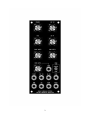
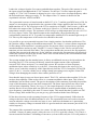
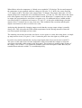
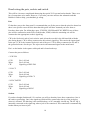
Oakley Sound Systems
5U Oakley Modular Series
One of Three
Voltage Controlled Oscillator
PCB Issue 6
Builder’s Guide
V6.2.2
Tony Allgood B.Eng PGCE
Oakley Sound Systems
CARLISLE
United Kingdom
1
2
Introduction
This is the Project Builder's Guide for the issue 6 VCO 5U module from Oakley Sound.
This document contains a basic introduction to the board, a description of the schematic, a full parts
list for the components needed to populate the boards, a list of the various interconnections and
some basic testing methods.
For the User Manual, which contains an overview of the operation of the unit, the history of the
various board issues, and all the calibration procedures, please visit the main project webpage at:
http://www.oakleysound.com/vco.htm
For general information regarding where to get parts and suggested part numbers please see our
useful Parts Guide at the project webpage or http://www.oakleysound.com/parts.pdf.
For general information on how to build our modules, including circuit board population, mounting
front panel components and making up board interconnects please see our generic Construction
Guide at the project webpage or http://www.oakleysound.com/construct.pdf.
3
The issue 6 printed circuit board set
The issue 6 main board PCB with issue 5 pot and socket boards fitted to a natural finish Schaeffer panel. The
board interconnects are Molex KK 0.1” types.
The main PCB is 108 mm (depth) x 144 mm (height) in size. All three boards use double sided
copper traces and have through plated holes. The solder pads are large and are easy to solder and
de-solder if necessary. They have a high quality solder mask on both sides for easier soldering, and
have clear legending on the component side for easier building.
If you are building the standard design there are no components mounted off the boards. All
components including sockets and pots are soldered directly to the boards.
Previously, many Oakley modules have had the sockets, switches and extra pots wired to the board
by individual wires. This module allows all the socket wiring to be done via the socket PCB and
two MTA solderless or Molex connections. If you are building this module in the standard Oakley
format this new system will reduce assembly time and possible wiring errors.
Some people will wish to use this Oakley design in a non standard format, such as fitting it to
another manufacturer’s rack or one of their own invention. This is perfectly easy to do. Simply do
not use the socket board and wire the main board to the sockets as per usual.
I have provided space for the three main control pots on the PCB. If you use the specified 16mm
Alpha pots and matching brackets, the PCB can be held firmly to the panel without any additional
mounting procedures. The pot spacing is 1.625” and is the same as the vertical spacing on the
MOTM modular synthesiser and most of our other modules.
4
Power supply requirements
The design requires plus and minus 15V supplies. The power supply should be adequately
regulated. The current consumption is about 30mA for each rail. Power is routed onto the PCB by a
four way 0.156” MTA156 type connector or the special five way Synthesizers.com MTA100
header. You could, of course, wire up the board by soldering on wires directly. The four pins on the
four way header are +15V, ground, earth/panel ground, -15V. The earth/panel connection allows
you to connect the metal front panel to the power supply’s ground without it sharing the modules’
ground line. More about this later.
Circuit Description
The VCO circuit can be thought of as several little subsections connected together. Let us look at
these little sections separately.
The first thing to look at is the power supply. This is shown on the bottom of the second sheet of the
schematics. The VCO could have been powered by +/-15V, but I wanted the VCO to sound like a
minimoog. To do this, I have used the same voltage levels within the VCO core as the original.
Thus we need to generate stable +10V and +5V supplies. I still used the +/-15V supply for most of
the op-amps as this would not have any affect on the waveforms.
Power enters the board on a 4-way MTA156 connector (PWR) or modified six way MTA100
header (PWR2). It is filtered initially by two small ferrite inductors, and decoupled by C20 to C23.
These prevent stray high frequency pulses from entering or leaving the unit by the power supply
lines. A LM723 voltage regulator IC is used to provide the 10V. This is an old IC design, some 30
years, but it is a superb device and has very low noise. The only problem is that you have to set the
output manually. PSU is a trimmer to set the voltage to be exactly 10.00V. The PCB has been laid
out for a 6mm cermet trimmer for long term stability.
Additional power supply decoupling is provided to each set of op-amps and ICs. This prevents any
reset pulses from travelling down the power supplies and soft synching the other VCOs in your
system.
To find the next part of the power supply we need to look at the first sheet of the schematics. Two
sections on this page generate the stable +5V and -10V required by the VCO.
U2 (pins 5, 6, 7) provides the +5V supply, by simply buffering half the +10V rail. An LT1013 is
specified to provide a very stable output.
U3 (pins 1, 2, 3) is a simple inverter circuit that produces a very stable -10.00V supply for the tune
pots and trimmers. Together with the stable +10.00V supply, this prevents any perturbations in the
+/-15V supply rails from affecting the tuning of the VCO. In reality, the tolerance of the 22K
resistors may mean that the output is not exactly -10.00V. This is perfectly OK, since we are not
interested in the actual value so much, but the stability. Those 22K resistors are metal film and their
value will not change appreciably over the years or at differing temperatures.
The VCO’s pitch is determined by a variety of sources. Two 1V/octave CV inputs, and two pots on
the front panel, and a trimmer to set initial frequency. U2 (pins 1, 2, 3) is built as a voltage summer.
5
It takes the voltages from the five sources and adds them together. The gain of the summer is set by
the input resistors and R44 and the V/OCT trimmer. For the two 1V/octave inputs the gain is
roughly -0.7. The V/OCT trimmer is adjusted to give a rise of one octave in output frequency when
the keyboard input voltage goes up by 1V. The output of the CV summer is then fed to the
exponential converter via R29 and R30.
The exponential converter is based around on half of U3 (5, 6, 7) and the quad NPN array of U4. Its
output is a current that is proportional to the exponent of the voltage applied at the base of the left
hand transistor of U4. The circuit gives the VCO a sensitivity of roughly -18mV/octave, so R29 and
R30 reduce the output of the CV summer to this level. However, it is worth noting that R30 is a
temperature sensitive resistor. The resistance of R30 will go up with temperature at a rate of 0.33%
for every degree Celsius. This should counteract the temperature effects produced by the
semiconductor junctions in U4. To get the best temperature stability R30 is mounted right on top of
U4. This way the temperature of the two devices should be the same.
It is possible to get an exponential response from a single transistor, but that has problems as Vbe,
the junction voltage, changes with ambient temperature. The ‘temp co’ resistor cannot compensate
for this change in the transistor’s operating current. So the now classic circuit with two perfectly
matched transistors and an op-amp, U4 and U3, is used. Changes in the Vbe for one half of the
transistor pair are mirrored in the other. The op-amp then matches the current in the first transistor
with the same current in the other one. So the collector current in the first transistor will effectively
control the collector current in the second. And it is the current drawn by the second transistor that
controls the frequency of the VCO.
The op-amp method also has another bonus, it allows an additional current to be injected into the
inverting pin of U3. This current will directly control the output current of the exponential
converter. R15 allows an input CV to control this current. We now have a linear frequency
modulation input, whose sensitivity is set by R15. Connecting this input to the wiper of a pot,
allows you to control the sensitivity of this input directly from the VCO’s front panel. D3 and U4
(pins 8, 9 & 10 – wired as a diode) act as voltage clamps preventing excess negative Linear FM
voltages from damaging the sensitive base-emitter junctions of U4.
Note that this input is not a true linear input control. This VCO, and most other modular VCOs, do
not have that capability. What we have here is a constant modulation index input. This is linear
modulation, but not linear control. The precise description of this statement is probably beyond the
scope of this document, but in a nut shell it means this: The linear input will not act with a strict
volt per hertz relationship. That is, for every 1V, the output frequency will not rise by a fixed
amount. But it will act so that audio rate FM will create a constant depth of modulation on any
given frequency controlled by the usual 1V/octave inputs. This means that the for audio rate FM
effects (clangs, bells and the like) you can get very good results with the linear FM input.
R3 has been chosen to set the operating frequency of the VCO at approximately 1kHz when the
voltage at the base of the left hand transistor is zero. The exponential converter works at its most
accurate when the voltage across the two bases is zero. And since the human ear is particularly
sensitive to frequency changes at around 1kHz it is good to make the most accurate part of the VCO
at this frequency.
The output of the exponential converter is a current. It is this current that controls the core of the
oscillator. Contrary to many people’s ideas, the core of a VCO is typically a linear CCO. That is a
current controlled oscillator. A doubling of current to (or from in this case) the CCO will produce a
6
doubling of output frequency.
The core of this VCO is a traditional sawtooth oscillator. C14 is the timing capacitor that is charged
by the output of the exponential converter. Since one end of C14 is tied to +5V, the voltage at the
other side of C14 moves towards zero volts as current is ‘sucked’ out of it. The higher the current
the faster the voltage drops. This voltage is ‘sniffed’ by one half of dual op-amp U5, which
produces a replica of this voltage at its output. Q4 aids the output of U5, as well as providing a
suitable offset for the triangle generator circuit (see later).
U7 (pins 1, 2, 3) is a comparator, and it is ‘watching’ the output of U5. When the voltage across
C14 reaches -5V, the output of U5 (pin1), normally at -15V, suddenly flies upward towards 10V.
This sudden level change passes through C13, and turns on JFET, Q3. This rapidly shorts out C14,
and the voltage across the capacitor drops to zero and both of its pins are at +5V once again. This
means that the voltage at the input of U8 is also at +5V, and the charging process begins again. C10
controls the time that the FET is on.
The sync input enables an external voltage to trip the comparator early. This will cause premature
shorting of the capacitor, locking the fundamental of the VCO to an incoming external sawtooth
signal. However, the fall time of the VCO’s saw waveform will still be set by the input CV to the
VCO. Thus, you will not get traditional sawtooth waveforms, but half completed sawteeth. The
sonic affects of these are marvellous, especially if you sweep your VCO with an envelope generator
whilst locked to another VCO at fixed frequency. The controlled VCO is often called the ‘slave’,
while the fixed VCO is called the ‘master’.
The incoming sync signal is first buffered by Q1, a simple emitter follower. This is shown on the
second page of the schematics. R11, C1 and C2 provide decoupling to prevent power supply noise
from accidental triggering of the VCO. The buffered signal is then passed to a simple differentiator
based around C9 (back on page one again). This part in conjunction with D1 and R24 only allow
only fast moving rising edges of the input waveform to reset the VCO core. In theory this should
allow any pulse wave to be used as sync waveforms, but the best sync sounds can be obtained when
a falling sawtooth master signal is used.
This last statement is very important if you want to use sync effectively. Use sawtooth outputs from
Oakley VCOs to sync other Oakley VCOs. MOTM VCOs produce rising ramps not falling
sawtooth waveforms. So you if you want to use a MOTM VCO as the master to sync a slave
Oakley VCO, then you must invert the MOTM’s output first. You could use an Oakley Multimix to
do the inversion.
The suggested layout of the Oakley VCO includes a depth control for the sync input. This will
allow you to create partial synching effects. This effect is very difficult to describe in words and has
to be heard to be believed. But very very complex timbres can be produced this way.
At high frequencies the VCO can go a little flat due to the finite time it takes to reset C14, and
errors in the exponential convertor. By lowering the maximum peak voltage of the sawtooth
waveform, the capacitor has less charge to loose before the output of U5 reaches zero. Thus the
frequency is higher than it would have been. Using a resistance in series with C14, we have a
voltage drop developed across the resistor that increases with frequency, due to the increased
current through the exponential convertor. This method was first postulated by Sergio Franco, and
is usually called ‘Franco’ compensation because of this. This works very well, but it does mean that
the amplitude of the sawtooth waveform decreases slightly with increasing frequency. In the first
7
two VCO issues I made this resistor variable. I was using the Franco resistance to compensate for
both reset time and errors in the exponential convertor. In the issue 6 VCO, this resistance is fixed
by R37, and is compensating for reset time only.
The exponential convertor causes errors due to ‘bulk emitter resistance’ or Rbe in the NPN pair, the
top half of the THAT300. Now the THAT300 is a very good matched pair with low values of Rbe,
but it still has an effect at very high frequencies of the VCO. Rbe is not a real resistor, but it acts as
if a resistor was connected in series with the emitter of the transistor.
In the early issue VCO boards, this loss of high frequency performance was cancelled out by the
effect of the Franco resistor. But really, this is a bit of a kludge since the Franco is designed to
compensate for a fixed timing error (the FET reset time), whilst Rbe causes an error related to
frequency. Over the limited range of an audio VCO, this is usually perfectly fine and Franco is used
in many commercial synth VCOs as the only high frequency compensation technique. For issue
three I decided to go one better. The newer issue VCOs use a fixed Franco resistor for the reset
time, and also use the Rossum technique to compensate for the exponential generators error.
Dave Rossum, founder of E-Mu systems in the 1970s, was an important player in the development
of the SSM chips. The SSM2030 VCO chip, which was not as good in comparison to the later
Curtis CEM3340, was ground breaking when it came out. Dave’s method of HF compensation for
the SSM2030 involved gently pulling the base of the first transistor of the NPN pair lower when the
collector current through the second NPN gets bigger.
In the issue 3 VCO I slavishly copied Dave’s idea as presented in Electronotes and indeed
implemented in the Prophet V many years ago. However, due to work done by René Schmitz this
simple method can be improved upon with the same number of components. As in the original
Rossum idea a fixed emitter resistor, R17, can be used to effectively measure the emitter current,
since the voltage on its bottom end will fall as collector current rises. Previously we took this
voltage, passed it through a diode to compensate for the base-emitter voltage drop (Vbe) of the
matched pair and then fed a small proportion of the resultant voltage back to the base of the left
hand transistor. This works well enough.
However, René’s idea improves on this on two counts. Firstly, the diode in the pure Rossum
method doesn’t exactly compensate for the Vbe because the current flowing in the diode and the
base-emitter junction are very much different. In the new circuit, both semiconductors see a similar
current as they are fed from identical resistive sources; R17 and the HFT trimmer are both the same
value. Therefore, the voltage drop across the 'diode' and Vbe should track each other reasonably
well, even over a change in ambient temperature. The 'diode' in the issue 6 VCO is actually the
base-emitter junction in a spare NPN transistor from the THAT300 array. One of the other benefits
of René’s method is that we feed the base of the left hand transistor with more or less the same
resistance which was not true of the original Rossum technique. So now the extra resistance due to
the HFT circuitry the left hand transistor base ‘sees’ is pretty much fixed at the value of R20 only.
Thus altering the HFT trimmer should not result in a change in the overall operating frequency of
the VCO as it did in the old method.
Going back to the VCO core: The sawtooth output from U5/Q2 is amplified by the other half of U5
(pins 5, 6, 7), before being sent to the output pad. The final output is roughly +5V to -5V, ie. 10V pp.
The triangle shaper is essentially a full wave rectifier, whose operating point is about 2.5V. If the
8
operating point is not exactly half the peak value of the sawtooth output of U5, then the triangle
wave will have discontinuities in it. This leads to a slightly brighter or harsher sound than the
perfect ‘textbook’ triangle waveform. SHP-T is a trimmer that allows precise enough adjustment in
the operating point to eliminate these glitches.
The created rectified wave is filtered before amplifying and level shifting by U6. The SYM-T
trimmer sets the DC offset of the wave output to match that of the sawtooth output. The final output
is again 10V p-p.
The sine wave shaper circuit, shown on page two of the schematics, acts upon the triangle wave
output. The rounded peaks of the sine wave are created by deliberately overdriving the inputs of one
half of U8, a dual operational transconductance amplifier (OTA). These devices are normally used
as VCAs, but in this VCO it is merely acting as a soft clipping unit. The non linearities of the
OTA’s input stage being utilised to squash the top and bottom peaks of the triangle wave input.
SHP-S adjusts the amount of overdrive. Since U8 gives a current output, it must be turned into a
voltage and this is done by U9 (pins 5, 6, 7).
R18 provides a special negative feedback path within the shaper circuit. This increases the nonlinearity of the whole stage at the critical peaks of the output waveform.
SYM-S provides compensation for the OTA’s own offset voltage. This offset voltage means that
the OTA will soft clip asymmetrically. By adding a small voltage of the opposite polarity to one of
the input pins, we can cancel the effects of the offset.
The sine wave created by this process does not give us a perfect textbook example of a sine wave.
However, the wave is very low in harmonics and for musical uses it is adequate.
The final output, and the final circuit block is the pulse conditioner. This is also found on page two
of the schematics. The first section of this is the CV summer and is based around U9 (pins 1, 2, 3).
This circuit simply sums together the PWM (pulse width modulation) CV input and the voltage
from the wiper of the Width pot. The output of the CV summer will go from around -5V to +5V
when being controlled by the Width pot alone.
The pulse wave generator itself is based around the second half of the comparator, U7 (pins 5, 6 &
7). This compares either the triangle wave or sawtooth wave output with a voltage set by the output
of the CV summer. If the waveform is higher than the voltage from the CV summer, the
comparator’s output goes low. If it is lower, the output goes high. Thus, the output is either low or
high, and spends very little time in between. This creates a rectangular waveform, where the
proportion of time spent high or low is controlled by the WIDTH pot and/or the external CV. If the
width pot is set to its middle position, and no input CV is applied, the output waveform should be a
square wave. The output of the comparator swings from -15V to ground (or zero volts).
The output of the comparator is out of phase with the audio input. Q2 inverts this signal, so that the
generated pulse wave will go high when the saw or triangle wave is high. It would be possible to
generate the correct phase by simply wiring the comparator’s inputs pins differently. Thus you
wouldn’t have to invert the output since it would already be the right way around. Earlier issues of
the VCO, in fact, did this. However, this caused a less than perfect output waveform. The positive
feedback provided by R40, which is needed for good comparator action, would cause the sawtooth
or triangle wave to be superposed to the output waveform. This was considered not to be a problem,
but with the new issue I decided to do things differently. And perhaps more correctly.
9
What follows after the comparator is, I think, new to modular VCO design. The inverted output of
the comparator is now summed with two voltages in U9 (pins 12, 13 &14). One comes from the
+15V supply via R74. The other is the output of the CV summer. The former allows the -15V/0V
output swing of the comparator to be normalised between +5V and -5V. The other allows the output
to be offset against zero volts as the pulse width is varied. When the CV summer has zero volts at
its output, the generated pulse waveform is a square wave. No additional offset is added and the
waveform from U9’s output moves between +5V and -5V. As the pulse width changes, then the
output of the CV summer moves away from zero. This is added to the waveform and the pulse
output waveform moves above or below zero volts.
Analysing this dynamically changing output reveals that the average output voltage is actually
always zero. This is because the offset added compensates for the altering amounts of time the
waveform spends in the high (or low) states.
The summing circuit also inverts the waveform, so once again, we create the wrong phase. A simple
op-amp inverter circuit, U9 (pins 9, 10 & 11) turns the pulse wave the right way round again.
If you do not want this dynamically varying output signal, then all you need to do is omit R71.
The source of the audio source for the comparator comes from either the triangle or sawtooth
waveforms selectable with a switch on the front panel. This selection is another unique feature of
the Oakley ‘One of three’ VCO. Both will sound the same with fixed pulse widths. But, they do
sound different when the width CV is modulated quickly.
10
Components
For general information regarding where to get parts and suggested part numbers please see our
useful Parts Guide at the project webpage or http://www.oakleysound.com/parts.pdf.
Some special considerations for this project
C14 is a close tolerance (2% or better) polystyrene capacitor or better. The PCB is laid out for
EXFS/HR series made by LCR. Farnell and others sell these. They are good components at a good
price.
The matched pair, THAT300P, can be difficult to trace, but it can be obtained at Farnell and THAT
Corp's distributor Profusion plc.
U2 and U3 should be low offset bi-polar dual op-amps. The LT1013C is to be recommended for
both its performance and cost. I used to recommend the OPA2277 but we now know of one case
where a particular batch of OPA2277 devices caused oscillation to the +5V reference voltage
The LM1458 is a real oldie, and some places don’t stock it any more. In the UK, Farnell and RS sell
the little chap for peanuts.
The LM13700N may be substituted with either the older 13600 (still made by JRC) and the well
and truly defunct Phillips’ NE5517.
The JFET is the J112, this is fairly common and is the same FET die as the original minimoog. But
take note, the Mini used the E112, and that has a different pin out.
11
The Temperature Coefficient Resistor
The positive temperature coefficient (PTC or temp co) resistor is a very special part. The ones I
recommend are 1W wirewound resistors with a nominal TC of +3500ppm/K. You can buy these
from us, KRL-Bantry in the US, or from Senso's Vintage Planet in the Netherlands. They are often
sold as equivalents to the old Tel Labs Q81 series which was used in the VCOs and VCFs of many
vintage synthesisers.
A close up of the exponential convertor on the issue 6 VCO. The THAT300 NPN array is mounted in a 14-pin DIL
socket and the 1K KRL temperature coefficient resistor straddles it. Note the small amount of thermal paste
between the resistor and the array.
The PTC resistor is fitted to the board so that it lies across the top of the THAT300 NPN array. A
bit of thermal compound (eg. Thermpath) could be used to keep the two devices in contact. You’ll
need to carefully bend the legs of the TC to make sure it lies flat on the surface of the THAT300
and still fits through its solder pads.
Important: Some specimens of the THAT300 have exposed metal sub-frames at the top (just
below the identifying notch) and at the bottom of the IC packaging. These tiny metal pieces are
connected to the chip's substrate and in the VCO will be connected to ground. It is essential that
these metal surfaces do not come into contact with the PTC's leads. Unfortunately, this is quite
possible as they reside close to where the leads come down past the THAT300's body. Please ensure
that the leads do not touch the THAT300's package on their way down to the PCB.
12
VCO issue 6 Parts List
For general information regarding where to get parts and suggested part numbers please see our
useful Parts Guide at the project webpage or http://www.oakleysound.com/parts.pdf.
The components are grouped into values, the order of the component names is of no particular
consequence.
A quick note on European part descriptions. R is shorthand for ohm. K is shorthand for kilo-ohm. R
is shorthand for ohm. So 22R is 22 ohm, 1K5 is 1,500 ohms or 1.5 kilohms. For capacitors: 1uF =
one microfarad = 1000nF = one thousand nanofarad.
To prevent loss of the small ‘.’ as the decimal point, a convention of inserting the unit in its place is
used. eg. 4R7 is a 4.7 ohm, 4K7 is a 4700 ohm resistor, 6n8 is a 6.8 nF capacitor.
Resistors
All 5% carbon 1/4W or better. Components designated as 1% should be 0.25W 1% metal film or
better.
22R
100R
390R
820R 1%
1K
1K +3500ppm/K Temp co.
2K
2K2
2K2 1%
5K1
5K6
6K2
6K2 1%
8K2
10K
10K 1%
18K
22K
22K 1%
33K
39K
39K 1%
47K
56K
62K
68K
68K 1%
100K
100K 1%
150K
R50, 42, 41, 60, 7, 75
R11
R19, 23
R37
R55, 62, 24, 56, 39, 67
R30
R25
R5
R22
R68
R65
R59
R21
R16, 69
R80, 78, 27, 70, 66, 48, 46, 49, 35, 10, 34
R2, 17, 57, 58
R79
R82, 73, 9, 71
R4, 6
R72, 77, 76
R47
R29
R12, 33
R63, 54
R18, 81
R74
R44
R36, 38, 13, 15, 61, 52, 51
R1, 32
R64
13
180K 1%
220K
270K
390K 1%
680K 1%
750K
1M
1M 1%
R28
R8
R53
R14, R40
R3, R45
R83
R26, R84, R43
R20, R31
Capacitors
18pF low-K 2.5mm ceramic
100pF low-K 2.5mm ceramic
220pF low-K 2.5mm ceramic
470pF low-K 2.5mm ceramic
1nF 1% polystyrene
100nF 63V polyester
2u2, 63V electrolytic
4u7, 35V electrolytic
10uF, 25V electrolytic
22uF, 25V electrolytic
C10
C13, 16
C9
C4, C8, 25
C14
C11, 12, 2, 23, 22
C20, 21
C18
C3
C15, 5, 7, 17, 6, 19, 24, 26, 1
Discrete Semiconductors
1N4148 signal diode
BAT42 Schottky diode
BC550 NPN transistor
J112 J-FET
D2, D3
D1
Q1, 2, 4, 5
Q3
Integrated Circuits
LM1458 dual bi-polar op-amp
LM13700 transconductance amp
LM2903 dual comparator
LM723 voltage regulator
LT1013CP low drift dual op-amp
THAT300P matched NPN quad array
TL074 quad bi-fet op-amp
TL072 dual bi-fet op-amp
U6
U8
U7
U1
U2, U3
U4
U9
U5
Trimmers
100K multiturn trimmer
10K multiturn trimmer
1K horizontal carbon trimmer
1K 6mm cermet trimmer
22K horizontal carbon trimmer
TUNE
V/OCT, HFT
SHP-T
PSU
SHP-S
14
47K horizontal carbon trimmer
SYM-S, SYM-T
Pots
50K or 47K Linear Alpha 16mm
DEPTH, WIDTH, TUNE-2, TUNE-1 on main board
EXP, LIN, SYNC on pot board
5 off
Alpha pot brackets
NB: Make sure you fit a slim washer in between the top pot on the pot board and the front panel.
This acts as a shim between the pot body and front panel alleviating stress on the pot legs. All the
other pots do not need this as they have pot brackets. The top pot on the issue 6 VCO main board
has the solder pads moved closer to the edge of the board so can be fitted directly against the front
panel. The main board does does not need the washer.
Miscellaneous
SPDT toggle switch
PWM type
1 off
3-way 0.1” header
Oakley Buss optional connector
1 off
Switchcraft 112APC
1/4” sockets mounted on socket board
9 off
4-way 0.1” MTA/Molex header
4-way 0.1” MTA/Molex housing
MAIN-2 (Main PCB and socket PCB)
MAIN-2 cable
2 off
2 off
5-way 0.1” MTA/Molex header
5-way 0.1” MTA/Molex housing
POTS (Pot PCB and socket PCB)
NSE cable
2 off
2 off
6-way 0.1” MTA/Molex header
6-way 0.1” MTA/Molex housing
MAIN-1 (Main PCB and socket PCB)
MAIN-1 cable
2 off
2 off
55mm 8-way jumper lead
LINK interconnect
1 off
MTA156 4 way header
MTA100 6-way header
PWR – Oakley/MOTM power supply
PWR2 – Synthesizers.com power supply
Leaded ferrite beads
L1, L2
You may well want to use sockets for the ICs. I would recommend low profile turned pin types as
these are the most reliable. You need one 16-pin DIL socket, three 14-pin DIL sockets, and five 8pin DIL sockets.
15
Wiring the sockets and switch using the VCO Socket Board
The general details of populating an Oakley socket board are given in our Construction Guide
however there are a few extra things that are worth mentioning. You not only have the sockets and
headers to fit but you also have a switch to attach to the socket board.
This is an Apem toggle switch mounted to a 3mm Schaeffer panel. Note the spring washer and nut behind the
panel. The nut at the front cannot be seen but it is the inside one that you need to use to secure the switch to the
panel.
Once you have soldered your headers and sockets into place remove the socket PCB from the panel
and fit your switch into the correct hole in the panel. Use the one of the nuts and the spring washer
on the inside of the panel. Use the second nut on the front of the panel but don't tighten it up. Only
thread it on so that all the nut is in place on the bush of the switch. Now use the inner nut to tighten
the switch to the panel. This way you won't scratch the front of the panel. Use a 5/16” open ended
spanner to do this but don't tighten it too much, it's only a little switch. It doesn’t matter which way
the switch goes in so long as the toggle moves up and down. Note you do not have to use the tagged
washer that the switch normally comes with. Now solder a short length of thin uninsulated solid
core wire to each of the three tangs. You can use some resistor lead clippings if you wish. Make
sure the wire leads stick up at right angles from the panel surface.
Now refit the socket PCB with all of its sockets back onto the front panel. Carefully align the three
wires from the switch through the three solder pads in the PCB. Now you can then flip the panel
over and fit all the sockets’ washers and nuts. Once this is done, you can solder the three switch
leads onto the PCB. Clip off any excess lead length that sticks out above the solder.
16
Connecting the VCO pot and socket boards
The first thing that will need doing is the interconnection between the pot and main board. This is
done with a 55mm long 8-way jumper connection. Simply thread all eight wires into six holes of
the LINK pads from the underside of the pot board. The other end of the jumper can then be gently
coerced into the LINK pads of the main board. Solder each end of the jumper. You must solder the
pot board from the top of that board, and the main board from the bottom of that board.
A close up of the 55mm long 8-way flexible interconnect between the main board and the pot board.
All the remaining interconnects will be made using either the MTA system or the slower, but
cheaper, Molex system.
Make up the 4-way interconnect first. This should be made from wires 100 mm long. Make sure
you get pin 1 going to pin 1 on the other housing, pin 2 to pin 2, etc. This cable will connect to the
headers called MAIN-2 on each board.
The second lead is a 5-way interconnect. This is made up to be 145 mm long. This should connect
the POTS headers on the socket board and the pot board.
The third lead is a 6-way interconnect. This is made up to be 90mm long. This will connect the
MAIN-1 headers on the main and socket boards.
You can use some cable ties to bundle the wires in each interconnect together. This is best done
once all the interconnects are in position.
17
Hand wiring the pots, sockets and switch
This will be a lot more complicated than using the special VCO pot and socket boards. There are a
lot of connections to be made. However, if you take your time and use the schematic and this
Builder's Guide to help, you shouldn't go wrong.
Pots
Fit the three pots to the front panel. I recommend that you fit the pots so that the pins face down but
there is no specific reason for this other than this guide will have assumed you have done so.
Pots have three pins. For all the three pots, EXP FM, LIN FM and SYNC DEPTH, two of these
pins will be connected to main PCB via the header, LINK, whilst the remaining one will be
connected to the appropriate socket's signal lug.
CW is the 'clockwise' end of pot's resistive track (from the rear this is the left hand side with the
pins facing down). CW is always connected to the socket's signal lug. This carries the input signal
to the pot. CCW is the 'counter-clockwise' end of the pot. CCW is always connected to 0V and is
the ground reference for the pot. The wiper carries the attenuated signal to the main board.
Pin 1 on the header is the square solder pad and is found at the top.
Connect the pots as follows:
1. EXP FM
CCW
Wiper
CW
Pin 1 of Link
Pin 2 of Link
Signal lug of EXP FM
2. LIN CV
CCW
Wiper
CW
Pin 3 of Link
Pin 4 of Link
Signal lug of LIN CV
3. SYNC DEPTH
CCW
Wiper
CW
Pin 5 of Link
Pin 6 of Link
Signal lug of SYNC
Sockets
If you have bought Switchcraft 112A sockets you will see that they have three connections. One is
the earth or ground tag. One is the signal tag which will be connected to the tip of the jack plug
when it is inserted. The third tag is the normalised tag, or NC (normally closed) tag. The NC tag is
internally connected to the signal tag when a jack is not connected. This connection is automatically
broken when you insert a jack.
18
Once fitted to the front panel the ground tags of each socket can be all connected together with solid
wire. I use 0.91mm diameter tinned copper wire for this job. It is nice and stiff, so retains its shape,
and you can make a neat framework that connects all the earth tags together. I would make it so that
the lower four sockets are joined with one long horizontal piece, the top row of four sockets with
another piece, and the PWM socket's earth tag the joined with a final vertical piece that straddles
both the lower two horizontal rows.
A single piece of insulated multistrand wire can then be used to connect all those connected earth
tags to pin 2 of the header labelled MAIN-2. Pin 1 is the square solder pad, so pin 2 is the one to the
left of that when looking at the topside of the board.
All the other remaining socket connections are connected to the signal or NC lugs of the sockets.
The tables below show the connections you need to make to the three headers, MAIN-1 and LINK:
MAIN-1
Pin
Pad name
Socket
Lug Type
Pin 1
Pin 2
Pin 3
Pin 4
Pin 5
Pin 6
Pulse
Sawtooth
Triangle
Sine
Mod
1V/OCT
PULSE
SAW
TRI
SINE
PWM
1V/OCT
Signal
Signal
Signal
Signal
Signal
Signal
Pin
Pad name
Socket
Lug Type
Pin 7
Pin 8
0V
0V
1V/OCT, EXP FM
LIN FM, PWM, SYNC
NC
NC
LINK
Switch
You should attach the switch to the front panel. Use the one of the nuts and the spring washer on the
inside of the panel. Use the second nut on the front of the panel but don't tighten it up. Only thread
it on so that all the nut is in place on the bush of the switch. Now use the inner nut to tighten the
switch to the panel. This way you won't scratch the front of the panel. Use a 5/16” open ended
spanner to do this but don't tighten it too much, it's only a little switch. It doesn’t matter which way
the switch goes in so long as the toggle moves up and down. You do not have to use the tagged
washer that the switch normally comes with.
The switch has three lugs or tangs. Each one is to be connected to the main board using the three
remaining empty solder pads on MAIN-2.
The top tang of the switch needs to be connected to pin 4 of MAIN-2. The middle tang to pin 1, the
square pad. The bottom tang to pin 3. Keep these wires as short as you can.
19
Power supply connections
Power connections – MOTM and Oakley
The PWR power socket is 0.156” MTA 4-way header. Friction lock types are recommended. This
system is compatible with MOTM systems.
Power
Pin number
+15V
Module GND
Earth/PAN
-15V
1
2
3
4
The earth/pan connection has been provided to allow the ground tags of the jack sockets to be
connected to the powers supply ground without using the module’s 0V supply. Earth loops cannot
occur through patch leads this way, although screening is maintained. Of course, this can only work
if all your modules follow this principle.
Power connections – Synthesizers.com
The PWR2 power socket is to be fitted if you are using the module with a Synthesizers.com system.
In this case you should not fit the PWR header. The PWR2 header is a six way 0.1” MTA, but with
the pin that is in location 2 removed. In this way location 3 is actually pin 2 on my schematic,
location 4 is actually pin 5 and so on.
Power
Location number
Schematic Pin number
+15V
Missing Pin
+5V
Module GND
-15V
Not connected
1
2
3
4
5
6
1
2
3
4
5
+5V is not used on this module, so location 3 (pin 2) is not actually connected to anything on the
PCB.
If fitting the PWR2 header, you will also need to link out pins 2 and 3 of PWR. This connects the
panel ground with the module ground. Simply solder a solid wire hoop made from a resistor lead
clipping to join the middle two pads of PWR together.
20
Final Comments
If you have any problems with the module, an excellent source of support is the Oakley Sound
Forum at Muffwiggler.com. Paul Darlow and I are on this group, as well as many other users and
builders of Oakley modules.
If you can't get your project to work, then Oakley Sound Systems are able to offer a 'get you
working' service. If you wish to take up this service please e-mail me, Tony Allgood, at my contact
e-mail address found on the website. I can service either fully populated PCBs or whole modules.
You will be charged for all postage costs, any parts used and my time at 25GBP per hour. Most
faults can be found and fixed within one hour, and I normally return modules within a week. The
minimum charge is 25GBP plus return postage costs.
If you have a comment about this builder's guide, or have a found a mistake in it, then please do let
me know. But please do not contact me or Paul Darlow directly with questions about sourcing
components or general fault finding. Honestly, we would love to help but we do not have the time
to help everyone individually by e-mail.
Last but not least, can I say a big thank you to all of you who helped and inspired me. Thanks
especially to all those nice people on the Synth-diy and Analogue Heaven mailing lists and those at
Muffwiggler.com.
Tony Allgood at Oakley Sound
Cumbria, UK
© January 2011 – Updated December 2012
No part of this document may be copied by whatever means without my permission.
21