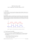
1
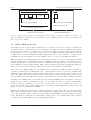
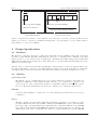
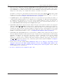
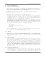
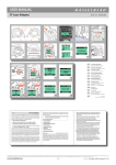
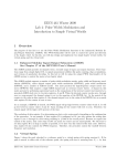
EECS 461 Winter 2009
Lab 3: Queued Analog-To-Digital Conversion
1
Overview
The purpose of this lab is to use the MPC5553 microcontroller to experiment with the operation and
triggering of analog to digital conversion. You should familiarize yourself with Chapter 19 in the Freescale
MPC5553 Reference Manual: “Enhanced Queued Analog-to-Digital Converter (eQADC).” It is also useful
to read through the Freescale Application Note AN2989 to understand how the MPC5553 ADC works.
1.1
Queued Analog-To-Digital Converter Module
Study Figure 19-1 in the MPC5553 Reference Manual. The eQADC module takes 40 single-ended analog
inputs from pins on the MPC5553. Internal multiplexers forward these signals to two analog to digital (A/D)
converters, ADC0 and ADC1. The eQADC is programmed by writing commands to a “first-in, first-out”
command buffer, CFIFO, also called a queue. This queue is used to determine how the ADC performs
conversions from its different input sources. Commands in this queue are executed in the order in which
they are written. The result of the analog-to digital conversion is a 12-bit number that is placed in a results
queue, RFIFO, which can be read directly by the processor. In this lab, we will use only the first converter,
ADC0.
When the results queue is filled or when the necessary conversions are finished, the contents of the RFIFO
have to be transferred to main memory. Direct Memory Access (DMA) allows for this transferring to happen
with minimal CPU involvement and this function is performed by the eDMA module on the MPC5553.
1.2
Queues
The eQADC system contains six CFIFO command queues, and six RFIFO result queues. At least one of the
command queues must be set up before the eQADC module will begin conversions. After being initialized, a
CFIFO will execute its command messages. In this lab we will make a list of command conversion messages
(CCM), maintained in an array. By programming our CCM array with a set of command conversion messages, conversions of the analog channels can be performed in any order, and results from the conversions
can be sent to any of the RFIFO queues. Results from the conversions can then be read from the RFIFO
in the order that the conversion commands were placed in the CFIFO. The format of command messages is
described in the MPC5553 reference manual in Section 19.4.1.2.
The QADC module requires a set of sequential commands specifying which channel to convert. The CFIFO
is a small internal queue, and the commands must be placed into this queue periodically so it does not
empty. If all command queues become empty, the ADC will stop processing until a command is available.
Since the internal queue is short, if we wish to continuously utilize the ADC, our program must place new
commands into the queue quite frequently. Typically, this would require a statement of code that is run
frequently, while interrupting the rest of the program from what it had been doing.
EECS 461: Embedded Control Systems
1
Winter 2009
Lab 3
Queued Analog-To-Digital Conversion
DSIZE
Number of commands total (CITER, BITER)
...
SSIZE,
SOFF
Destination copy address (DADDR)
Source copy address (SADDR)
DOFF, DLAST are both zero
Major-loop complete
source address adjustment (SLAST)
DMA source variable:
Continuous scan command list
DMA destination variable:
Command FIFO Push Register
Figure 1: Graphical representation of the Transfer Control Descriptor feeding the QADC. Note that for our
purposes, SSIZE and SOFF will be an equal number of bytes. DMA channel 0 is connected to CFIFO0, and
this corresponds to TCD 0.
1.3
Direct Memory Access
Interrupting the rest of the program is undesirable for a variety of reasons, the foremost of which is the
performance impact. Fortunately, there is a mechanism to automate data memory transfers without CPU
(and program) involvement. A transfer can be activated in a number of ways, typically either manually
by a statement of code, or by a peripheral as an event occurs. This mechanism is Direct Memory Access,
or DMA. There are 32 data transfers (32 DMA channels) that can be set up, waiting to be triggered by a
perhipheral. For more information about the eDMA module, see Section 9 of the MPC5553 manual.
When the ADC needs commands (if either the internal queue is empty, or is close to being empty), the ADC
can issue a DMA request. A DMA request causes the eDMA module on the MPC5553 to initiate a memory
transfer. The amount of memory and locations to transfer when this happens are governed by parameters
set in a Transfer Control Descriptor (TCD). Many of these parameters are presented graphically in Figure 1.
Refer to Section 9.3 in the manual for explanations about the terms mentioned in this figure.
In the case of the QADC CFIFO, at each DMA request we instruct the eDMA module to transfer one
conversion command into the CFIFO. The source of this transfer is the list of conversion commands. The
destination is the CFIFO write-command address. Each transfer is exactly the size of the conversion command. The DMA request is issued when the queue is emptying; the memory transfer fills the queue. In this
way, the CFIFO queue stays full without periodic program intervention, and the ADC continues converting.
We instruct the eDMA module to increment the source address (SADDR) after each transfer, so that it is
placing the next conversion command in the queue on each request. If our set of conversion commands has
length n, then after n transfers, we need to take a special action: we need to instruct the module to go
back to the beginning. We do this by using a major-loop-complete address adjustment, to subtract the total
length of our list of commands from SADDR.
Similarly, the QADC has an internal set of small queues that contain output values, or converted results.
When an internal queue is full, or almost full, the QADC fires a DMA request on a different channel than
before. We set up this request to transfer converted results from the RFIFO read-result address into a results
buffer. The TCD loops through the results buffer, resetting back to the beginning when it has completed
one full pass. The results TCD is presented graphically in Figure 2.
EECS 461: Embedded Control Systems
2
Winter 2009
Lab 3
Queued Analog-To-Digital Conversion
SSIZE
Number of results total (CITER, BITER)
...
DSIZE,
DOFF
Source copy address (SADDR)
Destination copy address (DADDR)
SOFF, SLAST are both zero
Major-loop complete
destination address adjustment (DLAST)
DMA destination variable:
Continuous scan result list
DMA source variable:
Result FIFO Pop Register
Figure 2: Graphical representation of the Transfer Control Descriptor removing conversion results from the
QADC. Note that for our purposes, DSIZE and DOFF will be an equal number of bytes. DMA channel 1
(with TCD 1) is connected to RFIFO0.
2
2.1
Design Specifications
Hardware
The interface board has connections to eight of the input pins from the eQADC module. The connections
are made to pins AN0 through AN7. Each input is connected to a four-pin header consisting of the input
signal, ground, a +5 volt reference and one unused pin. We will use the ADC as single-ended rather than
differential, meaning that we measure the voltage with respect to ground rather than measuring the voltage
difference between two pins.
A linear “slide” potentiometer is mounted permanently on the interface board for use with the ADC. Note
the jumper that must be connected to the AN1 signal pin for this to work, as shown in Figure 3. In this lab,
you will use this potentiometer as well as a sine wave from a function generator as input to the board.
2.2
Software
qadc.h and qadc.c
The first file, qadc.h, contains function prototypes for five functions. You will be responsible for
writing the definitions for these functions in the other file, qadc.c (rename qadc template.c). In
order to help you, some of these functions have been partially completed. As with Lab 2, place
the qadc.h file in the include directory and your completed qadc.c file in the lib directory.
Makefile
Use the provided makefile to compile your code. Place this file in your lab3 directory for proper
compilation.
lab3o.c
This file contains a program that buffers and sends ADC conversions to the serial port. The
program is implemented as a state-machine. During the CALIBRATE state, the program calculates
the average value of an input signal from a signal generator, and then transitions to the TRIGGER
state. The program waits in the TRIGGER state until the incoming signal is at a recognized point
during its period in order to synchronize the oscilloscope output, and then moves to the CAPTURE
EECS 461: Embedded Control Systems
3
Winter 2009
Lab 3
Queued Analog-To-Digital Conversion
Figure 3: Pin connection matrix between external signals and MPC5553 microcontroller.
state. While in the CAPTURE state, the program loops enough times to collect NUM SAMPLES
number of conversions. Then, during the SEND state, the program sends the captured data to
the computer using the serial port for display. The program executes the states in the order
CALIBRATE→TRIGGER→CAPTURE→SEND→CALIBRATE. . . . Place lab3o.c in the lab3 directory.
oscilloscope.exe
This file is a software oscilloscope program built using Matlab. When executed, the program reads
data from com1 of the serial port and then generates three plots. The first plot is a real-time plot
of the raw data received. The second plot is a real-time plot with a calibration applied to the X
and Y axes such that, after calibration, the Y-axis displays volts and the X-axis displays time.
The third plot is a frequency domain FFT plot of the data. This plot is convenient for observing
the frequency content of the input signal. An example of the display window is shown in Figure 4.
The purpose of this program is to observe the effects of oversampling and see the aliasing in the
frequency and time domains. We do this by sending the result of the AtoD conversion through
a serial-port link to the oscilloscope program running on the lab-station desktop.
3
Pre-Lab Assignment
Pre-lab questions must be done individually and handed in at the start of your lab section. You must also,
with your partner, design an initial version of your software before you come to your lab section. Your
software does not need to be completely debugged, but obviously more debugging before coming to lab means
less time you will spend in the lab.
Within qadc.c, there are five functions: Three initialization functions, qadcInit, fillCCMTable, setupDMARequests,
a function to execute a software triggered single conversion, qadcReadQ1, and a function for continuous conversion, qadcReadQ2. The prototypes of these functions can be found in the qadc.h file and some of the
code has already been provided for you in qadc.c.
1. qadcInit: Three things need to be done to initialize the eQADC: configuring the conversion command
queues, configuring the ADC itself, and establishing a list of conversion messages. The structure to
access the eQADC registers is defined in mpc5553.h.
EECS 461: Embedded Control Systems
4
Winter 2009
Lab 3
Queued Analog-To-Digital Conversion
Figure 4: Sample waveform displayed using the oscilloscope program and lab3o.c.
First, the eQADC Module Configuration Register (EQADC MCR) and CFIFO Control Registers
(EQADC CFCRn) must be configured. Initialize the eQADC Module Configuration Register (EQADC MCR)
to zero (see Section 19.3.2.1 of the manual).
We want to set up two queues, one for single-scan conversions and one for continuous-scan conversions as described in Section 19.4.3.5. Configure EQADC CFCR0 for software-triggered single-scan,
and EQADC CFCR1 for software-triggered continuous-scan mode. The CFIFO control registers are
described in Section 19.3.2.6; Table 19-10 enumerates operating modes.
Next, the ADC0 control register, ADC0 CR, must be configured to enable conversions, disable external
multiplexing (since we have no off-chip A-to-D converters), and set the ADC clock prescaler. The
ADC control registers are described in Section 19.3.3.1 of the Freescale User’s Manual. Use a clock
prescaler of 10 (see Table 19-28 in the manual). Note that the ADC registers are not part of the CPU
accessible memory map and can only be accessed indirectly through configuration commands. This is
accomplished using the union adc config msg declared for you in qadc.h. Complete this function
where prompted.
2. fillCCMTable: You also need to build the command conversion message (CCM) list using the union
cfifo msg. The fillCCMTable function initializes the two sets of CCM lists. The channels to be
converted are passed in as parameters. The first function parameter is the single-scan channel. The
second and third parameters specify the size of and list of channels to continuously convert.
Section 19.4.1.2.1 in the Freescale manual describes the command and result message formats used for
on-chip ADC operation (see Table 19-34).
Of course, it is necessary to configure two CCM lists: once for the single conversion function, qadcReadQ1,
EECS 461: Embedded Control Systems
5
Winter 2009
Lab 3
Queued Analog-To-Digital Conversion
and one for the continuous conversion, qadcReadQ2. For the single-scan queue, you need to set the
end-of-queue bit to 1, and the external buffer bit to 0. For single scan, put the result of the conversion in RFIFO0; for continuous scan, put the result in RFIFO1. Format all results as right justified,
unsigned; no time stamp. Use a sample time duration of 64 ADC clock cycles.
To initiate a conversion, set the single-scan enable bit in the appropriate EQADC CFCR register. This
should be done for the continuous-conversion queue at the end of the initialization routine, to start the
continuous conversions. Complete this function where prompted.
3. setupDMARequests: The setupDMARequests function accepts an integer representing the number of
continuous-scan channels that have been configured, up to a maximum of 8. The function must initialize
two Transfer Control Descriptors: one for each of the two DMA channels we want to use. The size of
the conversion commands is 32 bits, or 4 bytes, and the size of the conversion result is 16 bits, or 2
bytes. This function has already been completed for you.
4. qadcReadQ1: This function should read the single-scan queue and return the result for the input pin
defined by SINGLE SCAN CHANNEL. It will clear the completion flag, initiate a single scan of Queue 1,
and wait for the completion of the scan. The 12-bit ADC result will be read as an unsigned value, and
is justified as defined in Figure 19-30 in the MPC5553 manual. Because of this justification, the results
we read are bit-shifted. Note that for this 0-5V 12-bit ADC, the value of the result we read from the
RFIFO for a full 5V input will not be 212 − 1. Complete this function where prompted.
5. qadcReadQ2: The qadcReadQ2 function accepts an integer, channel, with a value in the range specified
when the QADC is initialized. This parameter is the continuous-scan command number defined during
qadcInit. In this lab, for each of the 8 specified conversion commands, we have set the channel
number to be equal to the command position in the queue. Since queue 2 is continuously being
scanned, no conversion need be initiated. The function simply returns the appropriate value from the
CONT SCAN RESULTS array, which is being continuously updated with results from RFIFO1. Complete
this function where prompted.
6. Review section 1.3 that explains DMA. Summarize why we are using it, and using a block
diagram, show how the ADC, DMA channels 0 and 1, the CFIFO push register, the
RFIFO pop register, and the command and results queues, all fit together. Refer to 19.5.2
in the manual for more information.
7. Be sure to hand in your completed qadc.c file.
EECS 461: Embedded Control Systems
6
Winter 2009
Lab 3
4
Queued Analog-To-Digital Conversion
In-Lab Assignment
4.1
Basic Conversion Testing
1. Write a simple C program called lab3.c that uses the qadcInit, qadcReadQ1, and qadcReadQ2 functions
from qadc.c. In a continuous loop, use the qadcReadQ2 function to retrieve the values of the eight analog
inputs on the board and place them into an array named iAnalogQ2.
2. Compile and debug your lab3.c program using the given makefile and the gmake command.
3. Download the lab3.elf file to the board.
4. In the P&E debugger, add iAnalogQ2[1] to the variable watch window.
5. Run the lab3.c. Adjust the potentiometer to change the analog signal sent to the pin between 0 and 5
volts. Then, stop running lab3.c by clicking the ‘Stop’ button in the debugger. Verify that the value of
iAnalogQ2[1] has changed. (Note: iAnalogQ2[1] is the second index into the iAnalogQ2 array and
should hold the value of the second analog input pin on the interface board).
Using a wire jumper, move the potentiometer input to each of the other seven pins to verify that the
qadcReadQ2 function is returning the values properly. (Note: You are not required to remove power
from either of the boards or reset the processor in order to move the potentiometer from one input to
the other.) Return the plastic jumper to AN1 once you have finished testing all the input pins. You
may also use the serial I/O functions to watch a value using code similar to:
char buff[32];
sprintf(buff, "\fvalue = %i", value);
puts(buff);
6. Verify the qadcReadQ1 function by creating a variable named iAnalogQ1. Use a procedure similar to
the one used above to verify that qadcReadQ1 is working correctly.
4.2
Timing
7. Modify your lab3.c file so that, before the call to qadcReadQ1 function, one of the LEDs is set to high
and is set back to low after the function returns. Connect an oscilloscope to the GPO output pin and
measure: 1) how long it takes for a scan to be completed on Q1, and 2) the periodic rate at which
scans occur.
4.3
Speed Testing
8. Change your lab3.c file so that when the ‘AN0’ input is measured in Queue 1 as being greater than 8192
(approximately half of the maximum value for the A/D conversion), a digital output is set to output
high. Otherwise, the digital output will output low. Connect a function generator to the ‘AN0’ signal
pin. Use an oscilloscope to observe both the input signal and the output signal. Use the stop and run
features on the oscilloscope to freeze the waveform. The sine wave input will result in a square wave
output of the same frequency as the input. Increase the input frequency and observe what happens
to the output. Does the frequency of the square wave continue to match that of the sine wave? Note
the frequency at which a change occurs. Continue to vary the frequency to obtain insight into the
phenomena you observe.
4.4
Oscilloscope Application
9. Compile using gmake scope and the lab3o.c file to build the software oscilloscope. Use the oscilloscope.exe program provided on the course website to plot the data automatically. Attach the signal
generator to your interface board as shown by your instructor. Demonstrate the working oscilloscope
EECS 461: Embedded Control Systems
7
Winter 2009
Lab 3
Queued Analog-To-Digital Conversion
to your instructor using a 0-5 volt sinusoid at 3 KHz. (Remember to put the signal generator in high-Z
mode).
It is intuitive that if the input signal is not sampled fast enough, the output of our oscilloscope program
will be incorrect. Think, for example, what would happen if we sampled a sine wave only once per
cycle: would the output waveform still look like a sine wave? More specifically, if a signal is under
sampled, the reconstructed wave form will be aliased, which means that high frequency components
of the input waveform will show up as low frequencies in the reconstructed signal. Consequently, you
will need to keep the input signal frequencies from the signal generator low in order to display them
properly. What is the highest-frequency signal you are able to capture and display without aliasing?
5
Post-Lab Assignment
1. Suppose that you need to read data and would like to have an accurate notion of what time the
data were sampled. What feature of the eQADC allows this? What field of a command
conversion request message (CCM) would you have to change to accomplish this? (Hint:
Consult the Freescale documentation in Section 19.4.1.2.)
2. Calibrating digital conversions to match a specific range of values is often desirable. What feature of
the eQADC allows this, and what field of a command conversion request message (CCM)
would you have to change to use it (19.4.1.2)? Lastly, briefly explain how this feature is
implemented in hardware (19.4.5.4.1).
3. In the lab exercise Section 4.3, you increased the frequency of an input sine wave until the frequency
of the square wave output did not match.Why does such a mismatch occur? What determines
the frequency at which a mismatch occurs?
4. Explain the differences between using a single-scan queue (qadcReadQ1) and a continuousscan queue (qadcReadQ2) to capture samples for an oscilloscope. Be sure to discuss:
(a) maximum conversion rate,
(b) the likelihood of sample jitter (is each sample taken at pre-defined time since the last one, or does
the sample spacing change each time).
5. Include well documented copies of your qadc.c and lab3.c files.
If you have comments that you feel would help improve the clarity or direction of this assignment, please
include them following your postlab solutions.
EECS 461: Embedded Control Systems
8
Winter 2009