1
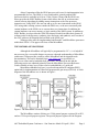
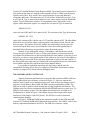
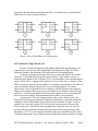
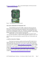
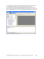
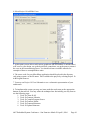
FPGA Softcores: the Microcontroller of Tomorrow?
Jerry H. Tucker
Robert H. Klenke
[email protected]
[email protected]
Virginia Commonwealth University
Gene S. Monroe
[email protected]
NASA: Langley Research Center
#407 Embedded System Conference – San Francisco March 29-April 1,2004
Page 1
INTRODUCTION
The microprocessor has proved to be the most significant development in
electronics since the invention of the transistor. The first microprocessors required many
discrete logic integrated circuits (IC’s) to form a complete computer, but in 1976 Intel
introduced the 8048 as the first 8-bit single-chip microcomputer [1]. The 8048 was soon
superseded by the 8051, variations of which are still widely used today. Over the years
single-chip microcomputers have undergone steady evolution and are available with a
wide range price, performance and capability levels. This has enabled them to be used to
implement countless embedded systems. In some embedded systems a microcomputer
may not require other IC’s, but typically additional digital logic is required to accomplish
the desired task. For complex systems, this additional logic may be substantial. By using
a programmable logic device (PLD) the additional digital logic can be implemented in a
single IC; thus, greatly reducing the chip count in embedded systems. Several years ago
at NASA Langley Research Center in Hampton, Virginia we developed a radiation hard
version of the 8051 and coupled that with a Xilinx field programmable gate array (FPGA)
to be used in reconfigurable embedded systems.
Not all embedded computer systems use a single-chip microcomputer. It has
occasionally proved to be cost effective to dedicate a conventional personal computer
(PC) to a single task; thus, effectively, making the PC serve as an embedded computer. It
is quite common to implement high performance embedded systems using an industry
standard backplane bus such as the PC-104. In addition miniature PC’s, smaller than PC104 modules, are available that can be used to implement embedded systems. It is
possible to incorporating an FPGA’s into such systems to reduce component count and
achieve reconfigurability.
As an example, the authors have developed two such systems. The first one is a
custom solution called the MERCAL (Minature Embedded Reconfigurable Computer
And Logic) module [2,3]. The MERCAL module consists of a custom printed circuit
board that contains a PC-based CPU board, in this case, a sub-credit card size DIMMPC
from JumpTec, and a Xilinx FPGA. The programming pins on the Xilinx FPGA are
directly connected to the parallel port on the DIMM PC, allowing it to re-program the
FPGA at any time under software control. A group of the general-purpose I/O pins of the
FPGA are connected to the PC’s ISA bus allowing for data transfer between the FPGA
and the software on the PC during system operation. The application program that runs
on the PC along with the FPGA configuration file can be uploaded to the PC so that the
system is reconfigurable.
A similar platform based on a PC-104 form factor has also been constructed by
the authors and used in implementing a hardware/software application. In this case, a
standard PC-104 CPU from WinSystems was combined with a Xilinx-based PC-104
FPGA board from Associated Professional Systems (APS). The APS board provides the
capability for the CPU to program the Xilinx FPGA by transferring programming data
across the PC-104 bus. Once programmed, like the MERCAL, the CPU and the FPGA
can exchange application data across the PC-104 bus during system operation.
These and similar systems are a precursor of a new way to think about digital
system design. This new paradigm has arrived because of the steady increase in the
#407 Embedded System Conference – San Francisco March 29-April 1,2004
Page 2
capability of FPGA’s. Today FPGA’s are available with the equivalent of over a million
logic gates. With these resources it is now possible to implement complex digital
systems, including one or more microcomputers, inside a single FPGA. This capability
presents the embedded system designer with exciting new opportunities along with
daunting challenges.
STATE-OF-THE-ART
Many programmable logic companies have introduced devices that allow the user
to combine general purpose processing with programmable logic on the same chip. Some
of these devices include a dedicated hard-core microcontroller with FPGA-based logic,
and others, like the Xilinx Microblaze, rely on a soft-core microcontroller that can be
implemented inside an FPGA with user logic.
Atmel Corporation offers a device it calls the FPSLIC, or Field Programmable
System Level Integrated Circuit. The FPSLIC device comes in several configurations, but
all include an 8-bit AVR microcontroller, memory that can be used to store program data
and code for the microcontroller, and FPGA resources that can be used to implement
application-specific user logic.
The Atmel AT94KAL devices combine the AVR microcontroller core with 36K
bytes of SRAM that can be used for data and instructions, and SRAM-based FPGA logic
that can implement up to 40K gates of logic. The AVR microcontroller is equipped with
an 8-bit hardware multiplier, 2 standard serial UARTS, and two 8-bit and one 16 bit
timer/counters that can be configured in various counter, capture, and PWM modes. The
general purpose I/O ports of the AVR are connected into the FPGA for interfacing to user
logic, and in addition, there are 16 address lines from the AVR into the FPGA to provide
device addressing and selection and 16 interrupt lines lead from the FPGA back to the
AVR. The AT94KAL devices are fabricated in a 0.35 mm, 5-metal layer, low power
CMOS process and provide 3.3V 33MHz PCI compliant outputs. The AVR
microcontroller is capable of 19 MIPS performance at a 25 MHz clock speed.
To support the FPSLIC devices, Atmel offers the System Designer tool, which
combines third-party design entry, simulation and synthesis tools with Atmel developed
place and route tools and third party compilers to provide a complete environment for
developing FPSLIC applications. One of the highlights of the System Designer
environment is the capability to co-simulate compiled application code running on the
AVR microcontroller with full debugging support, along with VHDL or Verilog models
of the user hardware to be implemented in the FPGA portion of the FPSLIC device.
Actel Corporation offers the Platform8051 environment for implementing
hardware/software systems. The environment is based on a soft-core version of the
industry standard ASM51 processor, a standardized 8-bit 8051 processor core. Actel also
has a number of additional cores available to interface the 8051 core to a 10/100
Ehternet, UART, I2C bus, and Serial Data Link Controller (SDLC). Platform8051
includes the Actel Libro toolset for design entry, synthesis, place and route, and
simulation, some of which are performed by included third-party tools, and a third-party
compiler for the 8051 core. Radiation hardened hardware/software applications can be
implemented in this architecture by utilizing Rad-Hard FPGAs available from Actel.
#407 Embedded System Conference – San Francisco March 29-April 1,2004
Page 3
Altera Corporation offers the NIOS processor soft-cores for implementation in its
programmable devices. The NIOS is a user configurable, general-purpose RISC
processor which is available in 16-bit or 32-bit versions. Along with the NIOS core,
Altera provides the SOPC Builder System which allows the user to accelerate timecritical software algorithms by adding custom instructions to the Nios processor
instruction set. Using SOPC, the user can add up to five new instructions to the NIOS
CPU using either existing resources inside the NIOS core, or the user can actually add
custom hardware to the NIOS core to execute these new instructions. In addition, the
custom hardware can access memory or logic outside of the NIOS system. In addition to
SOPC Builder, Actel provides the NIOS Developers Kit which includes their Quartus II
software tools for design entry, synthesis, place and route, and synthesis, and a version of
the GNU software development tools tailored to the NIOS core.
Xilinx provides tools for implementing both PowerPC and MicroBlace processors
within their FPGA’s. This paper will focus on the MicroBlaze.
THE MICROBLAZE PROCESSOR
Although the MicroBlaze will typically be programmed in C/C++, it is helpful if
not necessary for a successful designer to possess a through understanding of MicroBlaze
architecture. Xilinx provides extensive online MicroBlaze and development tools
documentation. This can be obtained form www.xilinx.com or specifically at
http://www.xilinx.com/ise/embedded/edk_docs.htm. The material in this and the
following section was obtained primarily form the MicroBlaze Processor Reference
Guide available at: http://www.xilinx.com/ise/embedded/mb_ref_guide.pdf.
MicroBlaze embedded soft core is a reduced instruction set computer (RISC)
optimized for implementation in Xilinx field program able gate arrays (FPGAs). A block
diagram of the MicroBlaze core is shown in Figure 1.
Figure 1. The MicroBlaze core block diagram.
The MicroBlaze consists of thirty-two 32-bit general purpose registers R0 to R31,
and two 32-bit special purpose registers. The special purpose registers are the Program
#407 Embedded System Conference – San Francisco March 29-April 1,2004
Page 4
Counter (PC) and the Machine Status Register (MSR). The general purpose register R0 is
also special in that when it is read the value returned is always 0. Other general purpose
registers such as R14, R16, and R17 have special purposes in servicing interrupts,
exceptions, and breaks. The instructions are 32-bits and are divided into two types, Type
A and Type B. Type A instructions usually have two source registers and one destination
register. Type B instructions contain a 16-bit immediate value, along with a source
register, and a destination register. For example the execution of Type A instruction
ADD R1, R2, R3
causes the sum of R2 and R3 to be placed in R1. The execution of the Type B instruction
ADDI R1, R2, 1234
replaces the contents of R1 with the sum of 1234 and the contents of R2. The MicroBlaze
instructions are executed in a three-segment pipeline consisting of Fetch, Decode, and
Execute stages. The pipeline effectively enables one instruction per clock cycle to be
executed except in those cases, such as branches, where the normal pipeline flow is
disrupted. Delayed branches are provided to reduce the branch penalty.
Memory is byte addressable, using a 32-bit address, and data memory can be
accessed as byte, half word (16-bits), or 32-bit words. Memory accesses must be datasize aligned. For halfword access the least significant bit of the address is forced to 0, and
for byte access the two least significant bits of the address are forced to 00. MicroBlaze is
a Big-Endian processor with bit 0 as the most significant or left most bit and word bit 31
the least significant or right most bit. Similarly the most significant byte of a word has the
lowest address and the least significant byte has the highest address.
It is possible to implement instruction and data caches, and the user has
considerable flexibility in how these are configured. MicroBlaze also features a debug
interface to support JTAG based software debugging tools.
THE MICROBLAZE BUS INTERFACE
Separate instruction and data buses are provided that conform to IBM’s OPB (onchip Peripheral Bus) specifications. As shown in Figure 3-1, there are separate bus
interface units for data access and instruction access. Each of these bus interface units is
split into a Local Memory Bus (LMB) and IBM’s On-chip peripheral bus (OPB). The
OPB can be used to connect to both on-chip and off-chip peripherals and memory. The
LMB provides for efficient synchronous block RAM (BRAM) transfers at rates up to 125
MHz for local memory systems. The MicroBlaze bus interfaces are available in six
configurations as shown in Figure 2. MicroBlaze also provides 8 input and 8 output
interfaces to Fast Simplex Link (FSL) busses. The FSL bus is used for dedicated
communication channels.
In Figure 2, IOPB and ILMB are the instruction interface to the OPB and LMB
respectively. Similarly DOPB and DLMB are the data interface. The LMB is used for fast
memory implemented internal to the FPGA. The OPB is use interface various
#407 Embedded System Conference – San Francisco March 29-April 1,2004
Page 5
peripherals, that are implemented within the FPGA, including memory controllers that
enable the use of large external memories.
Figure 2. The six MicroBlaze bus configurations.
DEVELOPMENT REQUIREMENTS
In order to begin development of MicroBlaze applications the minimum set of
required tools consists of the Xilinx Embedded Development Kit (EDK), the Xilinx
Integrated Synthesis Environment (ISE), and a hardware development board.
At the time of preparing this paper the latest version of the EDK is the recently
released 6.1. This EDK also requires the separate ISE 6.1i. This software can run on
Windows 2000, Windows XP, or Solaris 2.8/2.9. The MicroBlaze can be implemented in
various Xilinx FPGA’s ranging from Spartan II to Vertex II Pro devices. Because of the
FPGA resources required by the MicroBlaze it is probably unreasonable to select devices
with less capability than the Spartan IIE, even as a learning platform. For serious
applications, Vertex or Spartan-III devices should be selected. Hardware development
boards can be obtained form several sources including Avnet, Digilent, Memec Design,
and Xilinx. A Base System Builder Wizard provides support for a few selected boards,
and can be used to simplify implementations based on these selected boards.
An inexpensive first step learning platform, that we have found useful, is the
Digilent DE2 development board which contains a 200,000 gate equivalent Spartan IIE
combined with the Digilent DIO1 board. These boards are shown in Figure 3, and are
available for a total cost of about $150. They do not contain memory external to the
FPGA and the size of the FPGA limits the application complexity; however, they do
provide sufficient capability to implement designs that will develop proficiency with
MicroBlaze. At VCU we are using these boards in labs associated with the junior level
Computer Engineering class in Digital Systems. Information on these boards is available
#407 Embedded System Conference – San Francisco March 29-April 1,2004
Page 6
at http://www.digilentinc.com/, and it is expected that Digilent will shortly introduce
inexpensive boards with larger FPGA’s.
Figure 3. The Digilent DE2 and DIO1 boards.
THE XILINX EMBEDDED DEVELOPMENT KIT
The Embedded Development Kit (EDK) available from Xilinx provides the
hardware IP for the MicroBlaze processor and its peripherals, the Embedded System
Tools (EST), and associated documentation. Hardcopies of the documentation are not
provided, but can found online or in the “doc” sub-directory of the EDK. The software
tools necessary for MicroBlaze development are contained in the EST. A GUI, the Xilinx
Platform Studio (XPS), is used to invoke the tools in the EST.
With the XPS a user can configure the MicroBlaze processor and it’s busses,
connect the desired peripherals, compile and debug MicroBlaze application source code
using GNU tools, develop and simulate the required VHDL code, and download to the
FPGA.
A GETTING STARTED TUTORIAL
Space here does not permit a complete tutorial on using XPS, but the first few
steps are provided to give some indication of how the XPS works and to help get the
reader started. We expect to make one or more extensive tutorials, based on the latest
version of the EDK, available at http://www.people.vcu.edu/~jhtucker/. For this getting
started tutorial, we will use the Platform Studio flow. It is based on the EDK 6.1i (SP2)
with the ISE 6.1i (SP3) running on a Windows XP system. Xilinx currently provides,
available at http://www.xilinx.com/support/techsup/tutorials/edk_tutorials.htm, an EDK
6.1 MicroBlaze tutorial using the Base System Builder Wizard for the Memec Design
Virtex-II Pro board. Another useful tutorial, based on an older version of the EDK is
available at http://www.eece.unm.edu/xup/spartan2emicroblaze.htm.
#407 Embedded System Conference – San Francisco March 29-April 1,2004
Page 7
To use the XPS the steps are as follows:
Shortcut to XPS_GUI.exe.lnk
1. Open the XPS by selecting: Start à Xilinx Embedded Development Kit à Platform
Studio.
2. Select File à New Project à Platform Studio
#407 Embedded System Conference – San Francisco March 29-April 1,2004
Page 8
3. We will target this design to run on the Digilab DE2 board containing a Spartan IIE
XC2S200E in a PQ208 package. The design will be placed in the directory
c:_MicroBlaze\ESC_example. Fill in the appropriate information in the Create New
Project window and click on OK. When the windows appears asking if you want to start
with an empty MHS file, click on Yes. After reading the next message box click on OK.
#407 Embedded System Conference – San Francisco March 29-April 1,2004
Page 9
4. Select Project à Add/Edit Cores.
5. At this point you are able to add various peripherals (the MicroBlaze is included here)
as IP cores to your design, set up the desired bus connections, set up the ports to connect
the cores to the interconnecting buses. You should reference available tutorials for
examples of how to accomplish these tasks.
6. The source code for your MicroBlaze application should be placed in the directory
code using system.c as the file name. This is added to the project by selecting Project à
Add Program Sources.
7. You may use Project à View Schematic to see a schematic representation of your
architecture.
8. To implement the system you may use items under the tools menu or the appropriate
buttons on the task bar. You may refine the technique later but initially you may want to
use the following steps:
1. Tools à Clean à All.
2. Tools à Generate Libraries
3. Tools à Compile Program Source
4. Tools à Generate Netlist
5. Tools à Generate Bitstream
6. Tools à Update Bitstream
#407 Embedded System Conference – San Francisco March 29-April 1,2004
Page 10
At this point you may configure and run on your hardware by opening the Impact
program supplied with the ISE and download the file download.bit from the
implementation directory.
CONCLUSION
Programmable logic devices have evolved to the point that they contain sufficient
resources to implement microcontrollers, peripherals, and other logic within a single
PLD. Thus, the ability to produce system-on-a-chip devices is no longer restricted to
specialized ASIC designers. It is now possible, using relatively inexpensive tools, for any
designer with the sufficient knowledge to implement complex reconfigurable embedded
systems in FPGA’s.
The answer the question posed by the title of the paper requires qualification. It is
unlikely that FPGA softcores will entirely replace conventional microcontrollers;
however, the advantages offered by this emerging trend are so great that in the future we
expect it to be a dominant technology that cannot be ignored by embedded system
designers.
REFERENCES
[1] MCS-51 Family of Single-Chip Microcomputers User’s Manual, Intel Corporation,
July 1981
[2] Jerry H. Tucker, Robert H. Klenke, “An Embedded Reconfigurable Computer and
Logic Module: Final Report for NASA Langley Research Center” NASA grant NAG1-01042, Virginia Commonwealth University, June 2002.
[3] Robert H. Klenke, Jerry H. Tucker, Jason M. Blevins, “A New Hardware/Software
Codesign Environment and Senior Capstone Design Project for Computer
Engineering” 2003 International Conference on Microelectronic Systems Education,
Marriott Anaheim, California, June 1-2, 2003.
#407 Embedded System Conference – San Francisco March 29-April 1,2004
Page 11