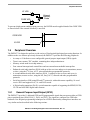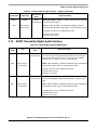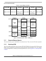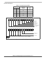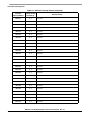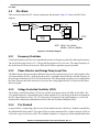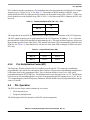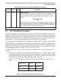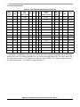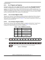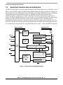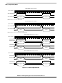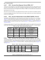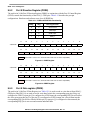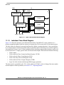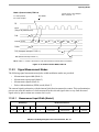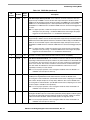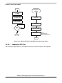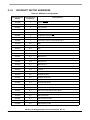
1
DSP56371 24-Bit Digital Signal
Processor
User Manual
Document Number: DSP56371UM
Rev. 2.1
08/2006
How to Reach Us:
Home Page:
www.freescale.com
E-mail:
[email protected]
USA/Europe or Locations Not Listed:
Freescale Semiconductor
Technical Information Center, CH370
1300 N. Alma School Road
Chandler, Arizona 85224
+1-800-521-6274 or +1-480-768-2130
[email protected]
Europe, Middle East, and Africa:
Freescale Halbleiter Deutschland GmbH
Technical Information Center
Schatzbogen 7
81829 Muenchen, Germany
+44 1296 380 456 (English)
+46 8 52200080 (English)
+49 89 92103 559 (German)
+33 1 69 35 48 48 (French)
[email protected]
Japan:
Freescale Semiconductor Japan Ltd.
Headquarters
ARCO Tower 15F
1-8-1, Shimo-Meguro, Meguro-ku,
Tokyo 153-0064, Japan
0120 191014 or +81 3 5437 9125
[email protected]
Asia/Pacific:
Freescale Semiconductor Hong Kong Ltd.
Technical Information Center
2 Dai King Street
Tai Po Industrial Estate
Tai Po, N.T., Hong Kong
+800 2666 8080
[email protected]
For Literature Requests Only:
Freescale Semiconductor Literature Distribution Center
P.O. Box 5405
Denver, Colorado 80217
1-800-521-6274 or 303-675-2140
Fax: 303-675-2150
[email protected]
Information in this document is provided solely to enable system and software implementers to use
Freescale Semiconductor products. There are no express or implied copyright licenses granted
hereunder to design or fabricate any integrated circuits or integrated circuits based on the information
in this document.
Freescale Semiconductor reserves the right to make changes without further notice to any products
herein. Freescale Semiconductor makes no warranty, representation or guarantee regarding the
suitability of its products for any particular purpose, nor does Freescale Semiconductor assume any
liability arising out of the application or use of any product or circuit, and specifically disclaims any
and all liability, including without limitation consequential or incidental damages. “Typical” parameters
that may be provided in Freescale Semiconductor data sheets and/or specifications can and do vary
in different applications and actual performance may vary over time. All operating parameters,
including “Typicals”, must be validated for each customer application by customer’s technical experts.
Freescale Semiconductor does not convey any license under its patent rights nor the rights of others.
Freescale Semiconductor products are not designed, intended, or authorized for use as components
in systems intended for surgical implant into the body, or other applications intended to support or
sustain life, or for any other application in which the failure of the Freescale Semiconductor product
could create a situation where personal injury or death may occur. Should Buyer purchase or use
Freescale Semiconductor products for any such unintended or unauthorized application, Buyer shall
indemnify and hold Freescale Semiconductor and its officers, employees, subsidiaries, affiliates, and
distributors harmless against all claims, costs, damages, and expenses, and reasonable attorney
fees arising out of, directly or indirectly, any claim of personal injury or death associated with such
unintended or unauthorized use, even if such claim alleges that Freescale Semiconductor was
negligent regarding the design or manufacture of the part.
Freescale™ and the Freescale logo are trademarks of Freescale Semiconductor, Inc. All other
product or service names are the property of their respective owners.
© Freescale Semiconductor, Inc. 2006. All rights reserved.
Contents
Preface
Document Summary . . . . . . . . . . . . . . . . . . . . . . . . . . . . . . . . . . . . . . . . . . . . . . . . . . . . . . . . xxiii
Revision History . . . . . . . . . . . . . . . . . . . . . . . . . . . . . . . . . . . . . . . . . . . . . . . . . . . . . . . . . . . . xxv
Manual Conventions . . . . . . . . . . . . . . . . . . . . . . . . . . . . . . . . . . . . . . . . . . . . . . . . . . . . . . . . . xxv
1
DSP56371 Overview
1.1
Introduction . . . . . . . . . . . . . . . . . . . . . . . . . . . . . . . . . . . . . . . . . . . . . . . . . . . . . . . . . . . . . . . . 1-1
1.2
DSP56300 Core Description . . . . . . . . . . . . . . . . . . . . . . . . . . . . . . . . . . . . . . . . . . . . . . . . . . . 1-2
1.3
DSP56371 Audio Processor Architecture . . . . . . . . . . . . . . . . . . . . . . . . . . . . . . . . . . . . . . . . . 1-4
1.4
DSP56300 Core Functional Blocks . . . . . . . . . . . . . . . . . . . . . . . . . . . . . . . . . . . . . . . . . . . . . . 1-4
1.4.1
Data ALU . . . . . . . . . . . . . . . . . . . . . . . . . . . . . . . . . . . . . . . . . . . . . . . . . . . . . . . . . . . . . . . 1-5
1.4.1.1
Data ALU Registers . . . . . . . . . . . . . . . . . . . . . . . . . . . . . . . . . . . . . . . . . . . . . . . . . . . . 1-5
1.4.1.2
Multiplier-Accumulator (MAC) . . . . . . . . . . . . . . . . . . . . . . . . . . . . . . . . . . . . . . . . . . 1-5
1.4.2
Address Generation Unit (AGU) . . . . . . . . . . . . . . . . . . . . . . . . . . . . . . . . . . . . . . . . . . . . . 1-5
1.4.3
Program Control Unit (PCU) . . . . . . . . . . . . . . . . . . . . . . . . . . . . . . . . . . . . . . . . . . . . . . . . 1-6
1.4.4
Internal Buses . . . . . . . . . . . . . . . . . . . . . . . . . . . . . . . . . . . . . . . . . . . . . . . . . . . . . . . . . . . 1-7
1.4.5
Direct Memory Access (DMA) . . . . . . . . . . . . . . . . . . . . . . . . . . . . . . . . . . . . . . . . . . . . . . 1-7
1.4.6
PLL-based Clock Oscillator . . . . . . . . . . . . . . . . . . . . . . . . . . . . . . . . . . . . . . . . . . . . . . . . . 1-7
1.4.7
On-Chip Memory . . . . . . . . . . . . . . . . . . . . . . . . . . . . . . . . . . . . . . . . . . . . . . . . . . . . . . . . . 1-8
1.4.8
Off-Chip Memory Expansion . . . . . . . . . . . . . . . . . . . . . . . . . . . . . . . . . . . . . . . . . . . . . . . 1-8
1.4.9
Power Requirements . . . . . . . . . . . . . . . . . . . . . . . . . . . . . . . . . . . . . . . . . . . . . . . . . . . . . . 1-8
1.5
Peripheral Overview . . . . . . . . . . . . . . . . . . . . . . . . . . . . . . . . . . . . . . . . . . . . . . . . . . . . . . . . . 1-9
1.5.1
General Purpose Input/Output (GPIO) . . . . . . . . . . . . . . . . . . . . . . . . . . . . . . . . . . . . . . . . 1-9
1.5.2
Triple Timer (TEC) . . . . . . . . . . . . . . . . . . . . . . . . . . . . . . . . . . . . . . . . . . . . . . . . . . . . . . 1-10
1.5.3
Enhanced Serial Audio Interface (ESAI) . . . . . . . . . . . . . . . . . . . . . . . . . . . . . . . . . . . . . . 1-10
1.5.4
Enhanced Serial Audio Interface 1 (ESAI_1) . . . . . . . . . . . . . . . . . . . . . . . . . . . . . . . . . . 1-10
1.5.5
Serial Host Interface (SHI) . . . . . . . . . . . . . . . . . . . . . . . . . . . . . . . . . . . . . . . . . . . . . . . . 1-10
1.5.6
Digital Audio Transmitter (DAX) . . . . . . . . . . . . . . . . . . . . . . . . . . . . . . . . . . . . . . . . . . . 1-10
2
Signal/Connection Descriptions
2.1
2.2
2.3
2.4
2.5
2.6
2.7
2.8
2.9
2.10
2.11
2.12
2.13
Signal Groupings . . . . . . . . . . . . . . . . . . . . . . . . . . . . . . . . . . . . . . . . . . . . . . . . . . . . . . . . . . . . 2-1
Power . . . . . . . . . . . . . . . . . . . . . . . . . . . . . . . . . . . . . . . . . . . . . . . . . . . . . . . . . . . . . . . . . . . . . 2-3
Ground . . . . . . . . . . . . . . . . . . . . . . . . . . . . . . . . . . . . . . . . . . . . . . . . . . . . . . . . . . . . . . . . . . . . 2-4
SCAN . . . . . . . . . . . . . . . . . . . . . . . . . . . . . . . . . . . . . . . . . . . . . . . . . . . . . . . . . . . . . . . . . . . . . 2-4
Clock and PLL . . . . . . . . . . . . . . . . . . . . . . . . . . . . . . . . . . . . . . . . . . . . . . . . . . . . . . . . . . . . . . 2-4
Interrupt and Mode Control . . . . . . . . . . . . . . . . . . . . . . . . . . . . . . . . . . . . . . . . . . . . . . . . . . . . 2-5
Serial Host Interface . . . . . . . . . . . . . . . . . . . . . . . . . . . . . . . . . . . . . . . . . . . . . . . . . . . . . . . . . 2-6
Enhanced Serial Audio Interface . . . . . . . . . . . . . . . . . . . . . . . . . . . . . . . . . . . . . . . . . . . . . . . . 2-9
Enhanced Serial Audio Interface_1 . . . . . . . . . . . . . . . . . . . . . . . . . . . . . . . . . . . . . . . . . . . . . 2-13
SPDIF Transmitter Digital Audio Interface . . . . . . . . . . . . . . . . . . . . . . . . . . . . . . . . . . . . . . 2-17
Dedicated GPIO Interface . . . . . . . . . . . . . . . . . . . . . . . . . . . . . . . . . . . . . . . . . . . . . . . . . . . . 2-18
Timer . . . . . . . . . . . . . . . . . . . . . . . . . . . . . . . . . . . . . . . . . . . . . . . . . . . . . . . . . . . . . . . . . . . . 2-19
JTAG/OnCE Interface . . . . . . . . . . . . . . . . . . . . . . . . . . . . . . . . . . . . . . . . . . . . . . . . . . . . . . . 2-20
DSP56371 24-Bit Digital Signal Processor, Rev. 2.1
Freescale Semiconductor
iii
3
Memory Configuration
3.1
Data and Program Memory Maps . . . . . . . . . . . . . . . . . . . . . . . . . . . . . . . . . . . . . . . . . . . . . . . 3-1
3.1.1
Reserved Memory Spaces . . . . . . . . . . . . . . . . . . . . . . . . . . . . . . . . . . . . . . . . . . . . . . . . . . 3-6
3.1.2
Bootstrap ROM . . . . . . . . . . . . . . . . . . . . . . . . . . . . . . . . . . . . . . . . . . . . . . . . . . . . . . . . . . 3-6
3.1.3
Dynamic Memory Configuration Switching . . . . . . . . . . . . . . . . . . . . . . . . . . . . . . . . . . . . 3-7
3.1.4
External Memory Support . . . . . . . . . . . . . . . . . . . . . . . . . . . . . . . . . . . . . . . . . . . . . . . . . . 3-8
3.1.5
DMA and Memory . . . . . . . . . . . . . . . . . . . . . . . . . . . . . . . . . . . . . . . . . . . . . . . . . . . . . . . . 3-8
3.1.6
EFCOP and Memory . . . . . . . . . . . . . . . . . . . . . . . . . . . . . . . . . . . . . . . . . . . . . . . . . . . . . . 3-8
3.1.7
Memory BLOCKS . . . . . . . . . . . . . . . . . . . . . . . . . . . . . . . . . . . . . . . . . . . . . . . . . . . . . . . . 3-8
3.2
Memory Patch Module . . . . . . . . . . . . . . . . . . . . . . . . . . . . . . . . . . . . . . . . . . . . . . . . . . . . . . . 3-8
3.3
Internal I/O Memory Map . . . . . . . . . . . . . . . . . . . . . . . . . . . . . . . . . . . . . . . . . . . . . . . . . . . . 3-10
4
Core Configuration
4.1
Introduction . . . . . . . . . . . . . . . . . . . . . . . . . . . . . . . . . . . . . . . . . . . . . . . . . . . . . . . . . . . . . . . . 4-1
4.2
Operating Mode Register (OMR) . . . . . . . . . . . . . . . . . . . . . . . . . . . . . . . . . . . . . . . . . . . . . . . 4-1
4.2.1
RESERVED - Bits 4, 5, 10 - 15 and 23 . . . . . . . . . . . . . . . . . . . . . . . . . . . . . . . . . . . . . . . . 4-2
4.3
Operating Modes . . . . . . . . . . . . . . . . . . . . . . . . . . . . . . . . . . . . . . . . . . . . . . . . . . . . . . . . . . . . 4-2
4.4
Interrupt Priority Registers . . . . . . . . . . . . . . . . . . . . . . . . . . . . . . . . . . . . . . . . . . . . . . . . . . . . 4-3
4.5
DMA Request Sources . . . . . . . . . . . . . . . . . . . . . . . . . . . . . . . . . . . . . . . . . . . . . . . . . . . . . . . 4-11
4.6
PLL Initialization . . . . . . . . . . . . . . . . . . . . . . . . . . . . . . . . . . . . . . . . . . . . . . . . . . . . . . . . . . . 4-12
4.6.1
PLL Pre-Divider Factor (PD0-PD4) . . . . . . . . . . . . . . . . . . . . . . . . . . . . . . . . . . . . . . . . . 4-12
4.6.2
PLL Multiplication Factor (MF0-MF7) . . . . . . . . . . . . . . . . . . . . . . . . . . . . . . . . . . . . . . . 4-12
4.6.3
PLL Feedback Multiplier (OD1) . . . . . . . . . . . . . . . . . . . . . . . . . . . . . . . . . . . . . . . . . . . . 4-12
4.6.4
PLL Output Divide Factor (OD0-OD1) . . . . . . . . . . . . . . . . . . . . . . . . . . . . . . . . . . . . . . . 4-12
4.6.5
PLL Divider Factor (DF0-DF2) . . . . . . . . . . . . . . . . . . . . . . . . . . . . . . . . . . . . . . . . . . . . . 4-12
4.7
Device Identification (ID) Register . . . . . . . . . . . . . . . . . . . . . . . . . . . . . . . . . . . . . . . . . . . . . 4-12
4.8
JTAG Identification (ID) Register . . . . . . . . . . . . . . . . . . . . . . . . . . . . . . . . . . . . . . . . . . . . . . 4-13
5
PLL and Clock Generator
5.1
Introduction . . . . . . . . . . . . . . . . . . . . . . . . . . . . . . . . . . . . . . . . . . . . . . . . . . . . . . . . . . . . . . . .
5.2
PLL and Clock Signals . . . . . . . . . . . . . . . . . . . . . . . . . . . . . . . . . . . . . . . . . . . . . . . . . . . . . . .
5.3
PLL Block . . . . . . . . . . . . . . . . . . . . . . . . . . . . . . . . . . . . . . . . . . . . . . . . . . . . . . . . . . . . . . . . .
5.3.1
Frequency Predivider . . . . . . . . . . . . . . . . . . . . . . . . . . . . . . . . . . . . . . . . . . . . . . . . . . . . . .
5.3.2
Phase Detector and Charge Pump Loop Filter . . . . . . . . . . . . . . . . . . . . . . . . . . . . . . . . . . .
5.3.3
Voltage Controlled Oscillator (VCO) . . . . . . . . . . . . . . . . . . . . . . . . . . . . . . . . . . . . . . . . .
5.3.4
PLL DividerS . . . . . . . . . . . . . . . . . . . . . . . . . . . . . . . . . . . . . . . . . . . . . . . . . . . . . . . . . . . .
5.3.5
PLL Multiplication Factor (MF) . . . . . . . . . . . . . . . . . . . . . . . . . . . . . . . . . . . . . . . . . . . . .
5.4
PLL Operation . . . . . . . . . . . . . . . . . . . . . . . . . . . . . . . . . . . . . . . . . . . . . . . . . . . . . . . . . . . . . .
5.4.1
EXTAL Clock Input Division . . . . . . . . . . . . . . . . . . . . . . . . . . . . . . . . . . . . . . . . . . . . . . .
5.4.2
PLL Frequency Multiplication . . . . . . . . . . . . . . . . . . . . . . . . . . . . . . . . . . . . . . . . . . . . . . .
5.4.3
PLL Output Frequency (PLL Out) . . . . . . . . . . . . . . . . . . . . . . . . . . . . . . . . . . . . . . . . . . . .
5.5
Clock Generator . . . . . . . . . . . . . . . . . . . . . . . . . . . . . . . . . . . . . . . . . . . . . . . . . . . . . . . . . . . . .
5.5.1
Low-Power Divider (LPD) . . . . . . . . . . . . . . . . . . . . . . . . . . . . . . . . . . . . . . . . . . . . . . . . .
5.6
Operating Frequency (Fosc) . . . . . . . . . . . . . . . . . . . . . . . . . . . . . . . . . . . . . . . . . . . . . . . . . . .
5-1
5-1
5-2
5-2
5-2
5-2
5-2
5-3
5-3
5-4
5-4
5-5
5-6
5-7
5-7
DSP56371 24-Bit Digital Signal Processor, Rev. 2.1
iv
Freescale Semiconductor
5.7
5.8
5.9
PLL Programming Model . . . . . . . . . . . . . . . . . . . . . . . . . . . . . . . . . . . . . . . . . . . . . . . . . . . . . 5-7
PLL Initialization Procedure . . . . . . . . . . . . . . . . . . . . . . . . . . . . . . . . . . . . . . . . . . . . . . . . . . 5-11
PLL Programming Examples . . . . . . . . . . . . . . . . . . . . . . . . . . . . . . . . . . . . . . . . . . . . . . . . . . 5-13
6
General Purpose Input/Output
6.1
Introduction . . . . . . . . . . . . . . . . . . . . . . . . . . . . . . . . . . . . . . . . . . . . . . . . . . . . . . . . . . . . . . . .
6.2
Programming Model . . . . . . . . . . . . . . . . . . . . . . . . . . . . . . . . . . . . . . . . . . . . . . . . . . . . . . . . .
6.2.1
Port C Signals and Registers . . . . . . . . . . . . . . . . . . . . . . . . . . . . . . . . . . . . . . . . . . . . . . . .
6.2.2
Port D Signals and Registers . . . . . . . . . . . . . . . . . . . . . . . . . . . . . . . . . . . . . . . . . . . . . . . .
6.2.3
Port E Signals and Registers . . . . . . . . . . . . . . . . . . . . . . . . . . . . . . . . . . . . . . . . . . . . . . . .
6.2.4
Port F Signals and Registers . . . . . . . . . . . . . . . . . . . . . . . . . . . . . . . . . . . . . . . . . . . . . . . .
6.2.4.1
Port F Control Register (PCRF) . . . . . . . . . . . . . . . . . . . . . . . . . . . . . . . . . . . . . . . . . . .
6.2.4.2
Port F Direction Register (PRRF) . . . . . . . . . . . . . . . . . . . . . . . . . . . . . . . . . . . . . . . . .
6.2.4.3
Port F Data register (PDRF) . . . . . . . . . . . . . . . . . . . . . . . . . . . . . . . . . . . . . . . . . . . . .
6.2.5
Timer/Event Counter Signals . . . . . . . . . . . . . . . . . . . . . . . . . . . . . . . . . . . . . . . . . . . . . . . .
7
6-1
6-1
6-1
6-1
6-1
6-2
6-2
6-2
6-3
6-3
Serial Host Interface
7.1
Introduction . . . . . . . . . . . . . . . . . . . . . . . . . . . . . . . . . . . . . . . . . . . . . . . . . . . . . . . . . . . . . . . . 7-1
7.2
Serial Host Interface Internal Architecture . . . . . . . . . . . . . . . . . . . . . . . . . . . . . . . . . . . . . . . . 7-2
7.3
SHI Clock Generator . . . . . . . . . . . . . . . . . . . . . . . . . . . . . . . . . . . . . . . . . . . . . . . . . . . . . . . . . 7-3
7.4
Serial Host Interface Programming Model . . . . . . . . . . . . . . . . . . . . . . . . . . . . . . . . . . . . . . . . 7-3
7.4.1
SHI Input/Output Shift Register (IOSR)—Host Side . . . . . . . . . . . . . . . . . . . . . . . . . . . . . 7-5
7.4.2
SHI Host Transmit Data Register (HTX)—DSP Side . . . . . . . . . . . . . . . . . . . . . . . . . . . . . 7-6
7.4.3
SHI Host Receive Data FIFO (HRX)—DSP Side . . . . . . . . . . . . . . . . . . . . . . . . . . . . . . . . 7-6
7.4.4
SHI Slave Address Register (HSAR)—DSP Side . . . . . . . . . . . . . . . . . . . . . . . . . . . . . . . . 7-6
7.4.4.1
HSAR Reserved Bits—Bits 19, 17–0 . . . . . . . . . . . . . . . . . . . . . . . . . . . . . . . . . . . . . . 7-7
7.4.4.2
HSAR I2C Slave Address (HA[6:3], HA1)—Bits 23–20,18 . . . . . . . . . . . . . . . . . . . . . 7-7
7.4.5
SHI Clock Control Register (HCKR)—DSP Side . . . . . . . . . . . . . . . . . . . . . . . . . . . . . . . . 7-7
7.4.5.1
Clock Phase and Polarity (CPHA and CPOL)—Bits 1–0 . . . . . . . . . . . . . . . . . . . . . . . 7-7
7.4.5.2
HCKR Prescaler Rate Select (HRS)—Bit 2 . . . . . . . . . . . . . . . . . . . . . . . . . . . . . . . . . 7-9
7.4.5.3
HCKR Divider Modulus Select (HDM[7:0])—Bits 10–3 . . . . . . . . . . . . . . . . . . . . . . . 7-9
7.4.5.4
HCKR Reserved Bits—Bits 23–11 . . . . . . . . . . . . . . . . . . . . . . . . . . . . . . . . . . . . . . . . 7-9
7.4.6
SHI Control/Status Register (HCSR)—DSP Side . . . . . . . . . . . . . . . . . . . . . . . . . . . . . . . . 7-9
7.4.6.1
HCSR Host Enable (HEN)—Bit 0 . . . . . . . . . . . . . . . . . . . . . . . . . . . . . . . . . . . . . . . . . 7-9
7.4.6.1.1
SHI Individual Reset . . . . . . . . . . . . . . . . . . . . . . . . . . . . . . . . . . . . . . . . . . . . . . . 7-10
7.4.6.2
HCSR I2C/SPI Selection (HI2C)—Bit 1 . . . . . . . . . . . . . . . . . . . . . . . . . . . . . . . . . . . 7-10
7.4.6.3
HCSR Serial Host Interface Mode (HM[1:0])—Bits 3–2 . . . . . . . . . . . . . . . . . . . . . . 7-10
7.4.6.4
HCSR I2C Clock Freeze (HCKFR)—Bit 4 . . . . . . . . . . . . . . . . . . . . . . . . . . . . . . . . . 7-10
7.4.6.5
HCSR FIFO-Enable Control (HFIFO)—Bit 5 . . . . . . . . . . . . . . . . . . . . . . . . . . . . . . . 7-11
7.4.6.6
HCSR Master Mode (HMST)—Bit 6 . . . . . . . . . . . . . . . . . . . . . . . . . . . . . . . . . . . . . 7-11
7.4.6.7
HCSR Host-Request Enable (HRQE[1:0])—Bits 8–7 . . . . . . . . . . . . . . . . . . . . . . . . 7-11
7.4.6.8
HCSR Idle (HIDLE)—Bit 9 . . . . . . . . . . . . . . . . . . . . . . . . . . . . . . . . . . . . . . . . . . . . 7-12
7.4.6.9
HCSR Bus-Error Interrupt Enable (HBIE)—Bit 10 . . . . . . . . . . . . . . . . . . . . . . . . . . 7-12
7.4.6.10
HCSR Transmit-Interrupt Enable (HTIE)—Bit 11 . . . . . . . . . . . . . . . . . . . . . . . . . . . 7-12
DSP56371 24-Bit Digital Signal Processor, Rev. 2.1
Freescale Semiconductor
v
7.4.6.11
HCSR Receive Interrupt Enable (HRIE[1:0])—Bits 13–12 . . . . . . . . . . . . . . . . . . . .
7.4.6.12
HCSR Host Transmit Underrun Error (HTUE)—Bit 14 . . . . . . . . . . . . . . . . . . . . . . .
7.4.6.13
HCSR Host Transmit Data Empty (HTDE)—Bit 15 . . . . . . . . . . . . . . . . . . . . . . . . . .
7.4.6.14
HCSR Reserved Bits—Bits 23, 18 and 16 . . . . . . . . . . . . . . . . . . . . . . . . . . . . . . . . .
7.4.6.15
Host Receive FIFO Not Empty (HRNE)—Bit 17 . . . . . . . . . . . . . . . . . . . . . . . . . . . .
7.4.6.16
Host Receive FIFO Full (HRFF)—Bit 19 . . . . . . . . . . . . . . . . . . . . . . . . . . . . . . . . . .
7.4.6.17
Host Receive Overrun Error (HROE)—Bit 20 . . . . . . . . . . . . . . . . . . . . . . . . . . . . . .
7.4.6.18
Host Bus Error (HBER)—Bit 21 . . . . . . . . . . . . . . . . . . . . . . . . . . . . . . . . . . . . . . . . .
7.4.6.19
HCSR Host Busy (HBUSY)—Bit 22 . . . . . . . . . . . . . . . . . . . . . . . . . . . . . . . . . . . . .
7.5
Characteristics Of The SPI Bus . . . . . . . . . . . . . . . . . . . . . . . . . . . . . . . . . . . . . . . . . . . . . . . .
7.6
Characteristics Of The I2C Bus . . . . . . . . . . . . . . . . . . . . . . . . . . . . . . . . . . . . . . . . . . . . . . . .
7.6.1
Overview . . . . . . . . . . . . . . . . . . . . . . . . . . . . . . . . . . . . . . . . . . . . . . . . . . . . . . . . . . . . . .
7.6.2
I2C Data Transfer Formats . . . . . . . . . . . . . . . . . . . . . . . . . . . . . . . . . . . . . . . . . . . . . . . . .
7.7
SHI Programming Considerations . . . . . . . . . . . . . . . . . . . . . . . . . . . . . . . . . . . . . . . . . . . . . .
7.7.1
SPI Slave Mode . . . . . . . . . . . . . . . . . . . . . . . . . . . . . . . . . . . . . . . . . . . . . . . . . . . . . . . . .
7.7.2
SPI Master Mode . . . . . . . . . . . . . . . . . . . . . . . . . . . . . . . . . . . . . . . . . . . . . . . . . . . . . . . .
7.7.3
I2C Slave Mode . . . . . . . . . . . . . . . . . . . . . . . . . . . . . . . . . . . . . . . . . . . . . . . . . . . . . . . . .
7.7.3.1
Receive Data in I2C Slave Mode . . . . . . . . . . . . . . . . . . . . . . . . . . . . . . . . . . . . . . . . .
7.7.3.2
Transmit Data In I2C Slave Mode . . . . . . . . . . . . . . . . . . . . . . . . . . . . . . . . . . . . . . . .
2C Master Mode . . . . . . . . . . . . . . . . . . . . . . . . . . . . . . . . . . . . . . . . . . . . . . . . . . . . . . . .
7.7.4
I
7.7.4.1
Receive Data in I2C Master Mode . . . . . . . . . . . . . . . . . . . . . . . . . . . . . . . . . . . . . . . .
7.7.4.2
Transmit Data In I2C Master Mode . . . . . . . . . . . . . . . . . . . . . . . . . . . . . . . . . . . . . . .
7.7.5
SHI Operation During DSP Stop . . . . . . . . . . . . . . . . . . . . . . . . . . . . . . . . . . . . . . . . . . . .
8
7-13
7-13
7-14
7-14
7-14
7-14
7-14
7-15
7-15
7-15
7-15
7-16
7-17
7-18
7-18
7-19
7-20
7-21
7-21
7-22
7-23
7-23
7-24
Enhanced Serial Audio Interface (ESAI)
8.1
Introduction . . . . . . . . . . . . . . . . . . . . . . . . . . . . . . . . . . . . . . . . . . . . . . . . . . . . . . . . . . . . . . . . 8-1
8.2
ESAI Data and Control Pins . . . . . . . . . . . . . . . . . . . . . . . . . . . . . . . . . . . . . . . . . . . . . . . . . . . 8-3
8.2.1
Serial Transmit 0 Data Pin (SDO0) . . . . . . . . . . . . . . . . . . . . . . . . . . . . . . . . . . . . . . . . . . . 8-3
8.2.2
Serial Transmit 1 Data Pin (SDO1) . . . . . . . . . . . . . . . . . . . . . . . . . . . . . . . . . . . . . . . . . . . 8-3
8.2.3
Serial Transmit 2/Receive 3 Data Pin (SDO2/SDI3) . . . . . . . . . . . . . . . . . . . . . . . . . . . . . . 8-3
8.2.4
Serial Transmit 3/Receive 2 Data Pin (SDO3/SDI2) . . . . . . . . . . . . . . . . . . . . . . . . . . . . . . 8-4
8.2.5
Serial Transmit 4/Receive 1 Data Pin (SDO4/SDI1) . . . . . . . . . . . . . . . . . . . . . . . . . . . . . . 8-4
8.2.6
Serial Transmit 5/Receive 0 Data Pin (SDO5/SDI0) . . . . . . . . . . . . . . . . . . . . . . . . . . . . . . 8-4
8.2.7
Receiver Serial Clock (SCKR) . . . . . . . . . . . . . . . . . . . . . . . . . . . . . . . . . . . . . . . . . . . . . . 8-4
8.2.8
Transmitter Serial Clock (SCKT) . . . . . . . . . . . . . . . . . . . . . . . . . . . . . . . . . . . . . . . . . . . . 8-5
8.2.9
Frame Sync for Receiver (FSR) . . . . . . . . . . . . . . . . . . . . . . . . . . . . . . . . . . . . . . . . . . . . . . 8-6
8.2.10
Frame Sync for Transmitter (FST) . . . . . . . . . . . . . . . . . . . . . . . . . . . . . . . . . . . . . . . . . . . 8-7
8.2.11
High Frequency Clock for Transmitter (HCKT) . . . . . . . . . . . . . . . . . . . . . . . . . . . . . . . . . 8-7
8.2.12
High Frequency Clock for Receiver (HCKR) . . . . . . . . . . . . . . . . . . . . . . . . . . . . . . . . . . . 8-7
8.3
ESAI Programming Model . . . . . . . . . . . . . . . . . . . . . . . . . . . . . . . . . . . . . . . . . . . . . . . . . . . . 8-8
8.3.1
ESAI Transmitter Clock Control Register (TCCR) . . . . . . . . . . . . . . . . . . . . . . . . . . . . . . . 8-8
8.3.1.1
TCCR Transmit Prescale Modulus Select (TPM7–TPM0) - Bits 7–0 . . . . . . . . . . . . . 8-8
8.3.1.2
TCCR Transmit Prescaler Range (TPSR) - Bit 8 . . . . . . . . . . . . . . . . . . . . . . . . . . . . . 8-9
8.3.1.3
TCCR Tx Frame Rate Divider Control (TDC4–TDC0) - Bits 13–9 . . . . . . . . . . . . . . 8-10
8.3.1.4
TCCR Tx High Frequency Clock Divider (TFP3-TFP0) - Bits 17–14 . . . . . . . . . . . . 8-11
DSP56371 24-Bit Digital Signal Processor, Rev. 2.1
vi
Freescale Semiconductor
8.3.1.5
8.3.1.6
8.3.1.7
8.3.1.8
8.3.1.9
8.3.1.10
8.3.2
8.3.2.1
8.3.2.2
8.3.2.3
8.3.2.4
8.3.2.5
8.3.2.6
8.3.2.7
8.3.2.8
8.3.2.9
8.3.2.10
8.3.2.11
8.3.2.12
8.3.2.13
8.3.2.14
8.3.2.15
8.3.2.16
8.3.2.17
8.3.2.18
8.3.2.19
8.3.3
8.3.3.1
8.3.3.2
8.3.3.3
8.3.3.4
8.3.3.5
8.3.3.6
8.3.3.7
8.3.3.8
8.3.3.9
8.3.3.10
8.3.4
8.3.4.1
8.3.4.2
8.3.4.3
8.3.4.4
8.3.4.5
8.3.4.6
8.3.4.7
TCCR Transmit Clock Polarity (TCKP) - Bit 18 . . . . . . . . . . . . . . . . . . . . . . . . . . . .
TCCR Transmit Frame Sync Polarity (TFSP) - Bit 19 . . . . . . . . . . . . . . . . . . . . . . . .
TCCR Transmit High Frequency Clock Polarity (THCKP) - Bit 20 . . . . . . . . . . . . .
TCCR Transmit Clock Source Direction (TCKD) - Bit 21 . . . . . . . . . . . . . . . . . . . . .
TCCR Transmit Frame Sync Signal Direction (TFSD) - Bit 22 . . . . . . . . . . . . . . . . .
TCCR Transmit High Frequency Clock Direction (THCKD) - Bit 23 . . . . . . . . . . . .
ESAI Transmit Control Register (TCR) . . . . . . . . . . . . . . . . . . . . . . . . . . . . . . . . . . . . . .
TCR ESAI Transmit 0 Enable (TE0) - Bit 0 . . . . . . . . . . . . . . . . . . . . . . . . . . . . . . . .
TCR ESAI Transmit 1 Enable (TE1) - Bit 1 . . . . . . . . . . . . . . . . . . . . . . . . . . . . . . . .
TCR ESAI Transmit 2 Enable (TE2) - Bit 2 . . . . . . . . . . . . . . . . . . . . . . . . . . . . . . . .
TCR ESAI Transmit 3 Enable (TE3) - Bit 3 . . . . . . . . . . . . . . . . . . . . . . . . . . . . . . . .
TCR ESAI Transmit 4 Enable (TE4) - Bit 4 . . . . . . . . . . . . . . . . . . . . . . . . . . . . . . . .
TCR ESAI Transmit 5 Enable (TE5) - Bit 5 . . . . . . . . . . . . . . . . . . . . . . . . . . . . . . . .
TCR Transmit Shift Direction (TSHFD) - Bit 6 . . . . . . . . . . . . . . . . . . . . . . . . . . . . .
TCR Transmit Word Alignment Control (TWA) - Bit 7 . . . . . . . . . . . . . . . . . . . . . . .
TCR Transmit Network Mode Control (TMOD1-TMOD0) - Bits 9-8 . . . . . . . . . . . .
TCR Tx Slot and Word Length Select (TSWS4-TSWS0) - Bits 14-10 . . . . . . . . . . .
TCR Transmit Frame Sync Length (TFSL) - Bit 15 . . . . . . . . . . . . . . . . . . . . . . . . . .
TCR Transmit Frame Sync Relative Timing (TFSR) - Bit 16 . . . . . . . . . . . . . . . . . .
TCR Transmit Zero Padding Control (PADC) - Bit 17 . . . . . . . . . . . . . . . . . . . . . . . .
TCR Reserved Bit - Bits 18 . . . . . . . . . . . . . . . . . . . . . . . . . . . . . . . . . . . . . . . . . . . . .
TCR Transmit Section Personal Reset (TPR) - Bit 19 . . . . . . . . . . . . . . . . . . . . . . . .
TCR Transmit Exception Interrupt Enable (TEIE) - Bit 20 . . . . . . . . . . . . . . . . . . . .
TCR Transmit Even Slot Data Interrupt Enable (TEDIE) - Bit 21 . . . . . . . . . . . . . . .
TCR Transmit Interrupt Enable (TIE) - Bit 22 . . . . . . . . . . . . . . . . . . . . . . . . . . . . . .
TCR Transmit Last Slot Interrupt Enable (TLIE) - Bit 23 . . . . . . . . . . . . . . . . . . . . .
ESAI Receive Clock Control Register (RCCR) . . . . . . . . . . . . . . . . . . . . . . . . . . . . . . . .
RCCR Receiver Prescale Modulus Select (RPM7–RPM0) - Bits 7–0 . . . . . . . . . . . .
RCCR Receiver Prescaler Range (RPSR) - Bit 8 . . . . . . . . . . . . . . . . . . . . . . . . . . . .
RCCR Rx Frame Rate Divider Control (RDC4–RDC0) - Bits 13–9 . . . . . . . . . . . . .
RCCR Rx High Frequency Clock Divider (RFP3-RFP0) - Bits 17-14 . . . . . . . . . . . .
RCCR Receiver Clock Polarity (RCKP) - Bit 18 . . . . . . . . . . . . . . . . . . . . . . . . . . . .
RCCR Receiver Frame Sync Polarity (RFSP) - Bit 19 . . . . . . . . . . . . . . . . . . . . . . . .
RCCR Receiver High Frequency Clock Polarity (RHCKP) - Bit 20 . . . . . . . . . . . . .
RCCR Receiver Clock Source Direction (RCKD) - Bit 21 . . . . . . . . . . . . . . . . . . . . .
RCCR Receiver Frame Sync Signal Direction (RFSD) - Bit 22 . . . . . . . . . . . . . . . . .
RCCR Receiver High Frequency Clock Direction (RHCKD) - Bit 23 . . . . . . . . . . . .
ESAI Receive Control Register (RCR) . . . . . . . . . . . . . . . . . . . . . . . . . . . . . . . . . . . . . . .
RCR ESAI Receiver 0 Enable (RE0) - Bit 0 . . . . . . . . . . . . . . . . . . . . . . . . . . . . . . . .
RCR ESAI Receiver 1 Enable (RE1) - Bit 1 . . . . . . . . . . . . . . . . . . . . . . . . . . . . . . . .
RCR ESAI Receiver 2 Enable (RE2) - Bit 2 . . . . . . . . . . . . . . . . . . . . . . . . . . . . . . . .
RCR ESAI Receiver 3 Enable (RE3) - Bit 3 . . . . . . . . . . . . . . . . . . . . . . . . . . . . . . . .
RCR Reserved Bits - Bits 5-4, 18-17 . . . . . . . . . . . . . . . . . . . . . . . . . . . . . . . . . . . . . .
RCR Receiver Shift Direction (RSHFD) - Bit 6 . . . . . . . . . . . . . . . . . . . . . . . . . . . . .
RCR Receiver Word Alignment Control (RWA) - Bit 7 . . . . . . . . . . . . . . . . . . . . . . .
8-11
8-11
8-11
8-11
8-12
8-12
8-12
8-12
8-13
8-13
8-13
8-14
8-14
8-15
8-15
8-15
8-17
8-18
8-20
8-20
8-20
8-20
8-20
8-21
8-21
8-21
8-21
8-22
8-22
8-22
8-22
8-23
8-23
8-23
8-23
8-24
8-24
8-25
8-25
8-26
8-26
8-26
8-26
8-26
8-26
DSP56371 24-Bit Digital Signal Processor, Rev. 2.1
Freescale Semiconductor
vii
8.3.4.8
RCR Receiver Network Mode Control (RMOD1-RMOD0) - Bits 9-8 . . . . . . . . . . . .
8.3.4.9
RCR Receiver Slot and Word Select (RSWS4-RSWS0) - Bits 14-10 . . . . . . . . . . . .
8.3.4.10
RCR Receiver Frame Sync Length (RFSL) - Bit 15 . . . . . . . . . . . . . . . . . . . . . . . . . .
8.3.4.11
RCR Receiver Frame Sync Relative Timing (RFSR) - Bit 16 . . . . . . . . . . . . . . . . . .
8.3.4.12
RCR Receiver Section Personal Reset (RPR) - Bit 19 . . . . . . . . . . . . . . . . . . . . . . . .
8.3.4.13
RCR Receive Exception Interrupt Enable (REIE) - Bit 20 . . . . . . . . . . . . . . . . . . . . .
8.3.4.14
RCR Receive Even Slot Data Interrupt Enable (REDIE) - Bit 21 . . . . . . . . . . . . . . . .
8.3.4.15
RCR Receive Interrupt Enable (RIE) - Bit 22 . . . . . . . . . . . . . . . . . . . . . . . . . . . . . . .
8.3.4.16
RCR Receive Last Slot Interrupt Enable (RLIE) - Bit 23 . . . . . . . . . . . . . . . . . . . . . .
8.3.5
ESAI Common Control Register (SAICR) . . . . . . . . . . . . . . . . . . . . . . . . . . . . . . . . . . . .
8.3.5.1
SAICR Serial Output Flag 0 (OF0) - Bit 0 . . . . . . . . . . . . . . . . . . . . . . . . . . . . . . . . .
8.3.5.2
SAICR Serial Output Flag 1 (OF1) - Bit 1 . . . . . . . . . . . . . . . . . . . . . . . . . . . . . . . . .
8.3.5.3
SAICR Serial Output Flag 2 (OF2) - Bit 2 . . . . . . . . . . . . . . . . . . . . . . . . . . . . . . . . .
8.3.5.4
SAICR Reserved Bits - Bits 5-3, 23-9 . . . . . . . . . . . . . . . . . . . . . . . . . . . . . . . . . . . . .
8.3.5.5
SAICR Synchronous Mode Selection (SYN) - Bit 6 . . . . . . . . . . . . . . . . . . . . . . . . . .
8.3.5.6
SAICR Transmit External Buffer Enable (TEBE) - Bit 7 . . . . . . . . . . . . . . . . . . . . . .
8.3.5.7
SAICR Alignment Control (ALC) - Bit 8 . . . . . . . . . . . . . . . . . . . . . . . . . . . . . . . . . .
8.3.6
ESAI Status Register (SAISR) . . . . . . . . . . . . . . . . . . . . . . . . . . . . . . . . . . . . . . . . . . . . .
8.3.6.1
SAISR Serial Input Flag 0 (IF0) - Bit 0 . . . . . . . . . . . . . . . . . . . . . . . . . . . . . . . . . . . .
8.3.6.2
SAISR Serial Input Flag 1 (IF1) - Bit 1 . . . . . . . . . . . . . . . . . . . . . . . . . . . . . . . . . . . .
8.3.6.3
SAISR Serial Input Flag 2 (IF2) - Bit 2 . . . . . . . . . . . . . . . . . . . . . . . . . . . . . . . . . . . .
8.3.6.4
SAISR Reserved Bits - Bits 5-3, 12-11, 23-18 . . . . . . . . . . . . . . . . . . . . . . . . . . . . . .
8.3.6.5
SAISR Receive Frame Sync Flag (RFS) - Bit 6 . . . . . . . . . . . . . . . . . . . . . . . . . . . . .
8.3.6.6
SAISR Receiver Overrun Error Flag (ROE) - Bit 7 . . . . . . . . . . . . . . . . . . . . . . . . . .
8.3.6.7
SAISR Receive Data Register Full (RDF) - Bit 8 . . . . . . . . . . . . . . . . . . . . . . . . . . . .
8.3.6.8
SAISR Receive Even-Data Register Full (REDF) - Bit 9 . . . . . . . . . . . . . . . . . . . . . .
8.3.6.9
SAISR Receive Odd-Data Register Full (RODF) - Bit 10 . . . . . . . . . . . . . . . . . . . . .
8.3.6.10
SAISR Transmit Frame Sync Flag (TFS) - Bit 13 . . . . . . . . . . . . . . . . . . . . . . . . . . . .
8.3.6.11
SAISR Transmit Underrun Error Flag (TUE) - Bit 14 . . . . . . . . . . . . . . . . . . . . . . . .
8.3.6.12
SAISR Transmit Data Register Empty (TDE) - Bit 15 . . . . . . . . . . . . . . . . . . . . . . . .
8.3.6.13
SAISR Transmit Even-Data Register Empty (TEDE) - Bit 16 . . . . . . . . . . . . . . . . . .
8.3.6.14
SAISR Transmit Odd-Data Register Empty (TODE) - Bit 17 . . . . . . . . . . . . . . . . . .
8.3.7
ESAI Receive Shift Registers . . . . . . . . . . . . . . . . . . . . . . . . . . . . . . . . . . . . . . . . . . . . . .
8.3.8
ESAI Receive Data Registers (RX3, RX2, RX1, RX0) . . . . . . . . . . . . . . . . . . . . . . . . . .
8.3.9
ESAI Transmit Shift Registers . . . . . . . . . . . . . . . . . . . . . . . . . . . . . . . . . . . . . . . . . . . . .
8.3.10
ESAI Transmit Data Registers (TX5, TX4, TX3, TX2,TX1,TX0) . . . . . . . . . . . . . . . . . .
8.3.11
ESAI Time Slot Register (TSR) . . . . . . . . . . . . . . . . . . . . . . . . . . . . . . . . . . . . . . . . . . . .
8.3.12
Transmit Slot Mask Registers (TSMA, TSMB) . . . . . . . . . . . . . . . . . . . . . . . . . . . . . . . .
8.3.13
Receive Slot Mask Registers (RSMA, RSMB) . . . . . . . . . . . . . . . . . . . . . . . . . . . . . . . . .
8.4
Operating Modes . . . . . . . . . . . . . . . . . . . . . . . . . . . . . . . . . . . . . . . . . . . . . . . . . . . . . . . . . . .
8.4.1
ESAI After Reset . . . . . . . . . . . . . . . . . . . . . . . . . . . . . . . . . . . . . . . . . . . . . . . . . . . . . . . .
8.4.2
ESAI Initialization . . . . . . . . . . . . . . . . . . . . . . . . . . . . . . . . . . . . . . . . . . . . . . . . . . . . . . .
8.4.3
ESAI Interrupt Requests . . . . . . . . . . . . . . . . . . . . . . . . . . . . . . . . . . . . . . . . . . . . . . . . . .
8.4.4
Operating Modes – Normal, Network and On-Demand . . . . . . . . . . . . . . . . . . . . . . . . . .
8.4.4.1
Normal/Network/On-Demand Mode Selection . . . . . . . . . . . . . . . . . . . . . . . . . . . . . .
8-27
8-27
8-28
8-29
8-29
8-29
8-29
8-29
8-30
8-30
8-30
8-30
8-30
8-31
8-31
8-31
8-31
8-32
8-33
8-33
8-33
8-33
8-33
8-34
8-34
8-34
8-34
8-34
8-35
8-35
8-35
8-35
8-39
8-39
8-39
8-39
8-39
8-40
8-41
8-42
8-42
8-42
8-43
8-44
8-44
DSP56371 24-Bit Digital Signal Processor, Rev. 2.1
viii
Freescale Semiconductor
8.4.4.2
Synchronous/Asynchronous Operating Modes . . . . . . . . . . . . . . . . . . . . . . . . . . . . . .
8.4.4.3
Frame Sync Selection . . . . . . . . . . . . . . . . . . . . . . . . . . . . . . . . . . . . . . . . . . . . . . . . .
8.4.4.4
Shift Direction Selection . . . . . . . . . . . . . . . . . . . . . . . . . . . . . . . . . . . . . . . . . . . . . . .
8.4.5
Serial I/O Flags . . . . . . . . . . . . . . . . . . . . . . . . . . . . . . . . . . . . . . . . . . . . . . . . . . . . . . . . .
8.5
GPIO - Pins and Registers . . . . . . . . . . . . . . . . . . . . . . . . . . . . . . . . . . . . . . . . . . . . . . . . . . . .
8.5.1
Port C Control Register (PCRC) . . . . . . . . . . . . . . . . . . . . . . . . . . . . . . . . . . . . . . . . . . . .
8.5.2
Port C Direction Register (PRRC) . . . . . . . . . . . . . . . . . . . . . . . . . . . . . . . . . . . . . . . . . . .
8.5.3
Port C Data register (PDRC) . . . . . . . . . . . . . . . . . . . . . . . . . . . . . . . . . . . . . . . . . . . . . . .
8.6
ESAI Initialization Examples . . . . . . . . . . . . . . . . . . . . . . . . . . . . . . . . . . . . . . . . . . . . . . . . .
8.6.1
Initializing the ESAI Using Individual Reset . . . . . . . . . . . . . . . . . . . . . . . . . . . . . . . . . .
8.6.2
Initializing Just the ESAI Transmitter Section . . . . . . . . . . . . . . . . . . . . . . . . . . . . . . . . .
8.6.3
Initializing Just the ESAI Receiver Section . . . . . . . . . . . . . . . . . . . . . . . . . . . . . . . . . . . .
9
8-44
8-45
8-45
8-45
8-46
8-46
8-46
8-47
8-48
8-48
8-49
8-49
Enhanced Serial Audio Interface 1 (ESAI_1)
9.1
Introduction . . . . . . . . . . . . . . . . . . . . . . . . . . . . . . . . . . . . . . . . . . . . . . . . . . . . . . . . . . . . . . . . 9-1
9.2
ESAI_1 Data and Control Pins . . . . . . . . . . . . . . . . . . . . . . . . . . . . . . . . . . . . . . . . . . . . . . . . . 9-3
9.2.1
Serial Transmit 0 Data Pin (SDO0_1) . . . . . . . . . . . . . . . . . . . . . . . . . . . . . . . . . . . . . . . . . 9-3
9.2.2
Serial Transmit 1 Data Pin (SDO1_1) . . . . . . . . . . . . . . . . . . . . . . . . . . . . . . . . . . . . . . . . . 9-3
9.2.3
Serial Transmit 2/Receive 3 Data Pin (SDO2_1/SDI3_1) . . . . . . . . . . . . . . . . . . . . . . . . . . 9-3
9.2.4
Serial Transmit 3/Receive 2 Data Pin (SDO3_1/SDI2_1) . . . . . . . . . . . . . . . . . . . . . . . . . . 9-4
9.2.5
Serial Transmit 4/Receive 1 Data Pin (SDO4_1/SDI1_1) . . . . . . . . . . . . . . . . . . . . . . . . . . 9-4
9.2.6
Serial Transmit 5/Receive 0 Data Pin (SDO5_1/SDI0_1) . . . . . . . . . . . . . . . . . . . . . . . . . . 9-4
9.2.7
Receiver Serial Clock (SCKR_1) . . . . . . . . . . . . . . . . . . . . . . . . . . . . . . . . . . . . . . . . . . . . 9-4
9.2.8
Transmitter Serial Clock (SCKT_1) . . . . . . . . . . . . . . . . . . . . . . . . . . . . . . . . . . . . . . . . . . 9-5
9.2.9
Frame Sync for Receiver (FSR_1) . . . . . . . . . . . . . . . . . . . . . . . . . . . . . . . . . . . . . . . . . . . . 9-6
9.2.10
Frame Sync for Transmitter (FST_1) . . . . . . . . . . . . . . . . . . . . . . . . . . . . . . . . . . . . . . . . . 9-6
9.2.11
High Frequency Clock for Transmitter (HCKT_1) . . . . . . . . . . . . . . . . . . . . . . . . . . . . . . . 9-7
9.2.12
High Frequency Clock for Receiver (HCKR_1) . . . . . . . . . . . . . . . . . . . . . . . . . . . . . . . . . 9-7
9.3
ESAI_1 Programming Model . . . . . . . . . . . . . . . . . . . . . . . . . . . . . . . . . . . . . . . . . . . . . . . . . . 9-7
9.3.1
ESAI_1 Transmitter Clock Control Register (TCCR_1) . . . . . . . . . . . . . . . . . . . . . . . . . . . 9-7
9.3.1.1
TCCR_1 Transmit Prescale Modulus Select (TPM7–TPM0) - Bits 7–0 . . . . . . . . . . . 9-8
9.3.1.2
TCCR_1 Transmit Prescaler Range (TPSR) - Bit 8 . . . . . . . . . . . . . . . . . . . . . . . . . . 9-10
9.3.1.3
TCCR_1 Tx Frame Rate Divider Control (TDC4–TDC0) - Bits 13–9 . . . . . . . . . . . . 9-10
9.3.1.4
TCCR_1 Tx High Frequency Clock Divider (TFP3-TFP0) - Bits 17–14 . . . . . . . . . . 9-11
9.3.1.5
TCCR_1 Transmit Clock Polarity (TCKP) - Bit 18 . . . . . . . . . . . . . . . . . . . . . . . . . . 9-12
9.3.1.6
TCCR_1 Transmit Frame Sync Polarity (TFSP) - Bit 19 . . . . . . . . . . . . . . . . . . . . . . 9-12
9.3.1.7
TCCR_1 Transmit High Frequency Clock Polarity (THCKP) - Bit 20 . . . . . . . . . . . 9-12
9.3.1.8
TCCR_1 Transmit Clock Source Direction (TCKD) - Bit 21 . . . . . . . . . . . . . . . . . . . 9-12
9.3.1.9
TCCR_1 Transmit Frame Sync Signal Direction (TFSD) - Bit 22 . . . . . . . . . . . . . . . 9-12
9.3.1.10
TCCR_1 Transmit High Frequency Clock Direction (THCKD) - Bit 23 . . . . . . . . . . 9-12
9.3.2
ESAI_1 Transmit Control Register (TCR_1) . . . . . . . . . . . . . . . . . . . . . . . . . . . . . . . . . . 9-12
9.3.2.1
TCR_1 ESAI_1 Transmit 0 Enable (TE0) - Bit 0 . . . . . . . . . . . . . . . . . . . . . . . . . . . . 9-13
9.3.2.2
TCR_1 ESAI_1 Transmit 1 Enable (TE1) - Bit 1 . . . . . . . . . . . . . . . . . . . . . . . . . . . . 9-13
9.3.2.3
TCR_1 ESAI_1 Transmit 2 Enable (TE2) - Bit 2 . . . . . . . . . . . . . . . . . . . . . . . . . . . . 9-14
9.3.2.4
TCR_1 ESAI_1 Transmit 3 Enable (TE3) - Bit 3 . . . . . . . . . . . . . . . . . . . . . . . . . . . . 9-14
DSP56371 24-Bit Digital Signal Processor, Rev. 2.1
Freescale Semiconductor
ix
9.3.2.5
9.3.2.6
9.3.2.7
9.3.2.8
9.3.2.9
9.3.2.10
9.3.2.11
9.3.2.12
9.3.2.13
9.3.2.14
9.3.2.15
9.3.2.16
9.3.2.17
9.3.2.18
9.3.2.19
9.3.3
9.3.3.1
9.3.3.2
9.3.3.3
9.3.3.4
9.3.3.5
9.3.3.6
9.3.3.7
9.3.3.8
9.3.3.9
9.3.3.10
9.3.4
9.3.4.1
9.3.4.2
9.3.4.3
9.3.4.4
9.3.4.5
9.3.4.6
9.3.4.7
9.3.4.8
9.3.4.9
9.3.4.10
9.3.4.11
9.3.4.12
9.3.4.13
9.3.4.14
9.3.4.15
9.3.4.16
9.3.5
9.3.5.1
TCR_1 ESAI_1 Transmit 4 Enable (TE4) - Bit 4 . . . . . . . . . . . . . . . . . . . . . . . . . . . .
TCR_1 ESAI_1 Transmit 5 Enable (TE5) - Bit 5 . . . . . . . . . . . . . . . . . . . . . . . . . . . .
TCR_1 Transmit Shift Direction (TSHFD) - Bit 6 . . . . . . . . . . . . . . . . . . . . . . . . . . .
TCR_1 Transmit Word Alignment Control (TWA) - Bit 7 . . . . . . . . . . . . . . . . . . . . .
TCR_1 Transmit Network Mode Control (TMOD1-TMOD0) - Bits 9-8 . . . . . . . . . .
TCR_1 Tx Slot and Word Length Select (TSWS4-TSWS0) - Bits 14-10 . . . . . . . . .
TCR_1 Transmit Frame Sync Length (TFSL) - Bit 15 . . . . . . . . . . . . . . . . . . . . . . . .
TCR_1 Transmit Frame Sync Relative Timing (TFSR) - Bit 16 . . . . . . . . . . . . . . . .
TCR_1 Transmit Zero Padding Control (PADC) - Bit 17 . . . . . . . . . . . . . . . . . . . . . .
Reserved - Bit 18 . . . . . . . . . . . . . . . . . . . . . . . . . . . . . . . . . . . . . . . . . . . . . . . . . . . . .
TCR_1 Transmit Section Personal Reset (TPR) - Bit 19 . . . . . . . . . . . . . . . . . . . . . .
TCR_1 Transmit Exception Interrupt Enable (TEIE) - Bit 20 . . . . . . . . . . . . . . . . . .
TCR_1 Transmit Even Slot Data Interrupt Enable (TEDIE) - Bit 21 . . . . . . . . . . . . .
TCR_1 Transmit Interrupt Enable (TIE) - Bit 22 . . . . . . . . . . . . . . . . . . . . . . . . . . . .
TCR_1 Transmit Last Slot Interrupt Enable (TLIE) - Bit 23 . . . . . . . . . . . . . . . . . . .
ESAI_1 Receive Clock Control Register (RCCR_1) . . . . . . . . . . . . . . . . . . . . . . . . . . . .
RCCR_1 Receiver Prescale Modulus Select (RPM7–RPM0) - Bits 7–0 . . . . . . . . . .
RCCR_1 Receiver Prescaler Range (RPSR) - Bit 8 . . . . . . . . . . . . . . . . . . . . . . . . . .
RCCR_1 Rx Frame Rate Divider Control (RDC4–RDC0) - Bits 13–9 . . . . . . . . . . .
RCCR_1 Rx High Frequency Clock Divider (RFP3-RFP0) - Bits 14-17 . . . . . . . . . .
RCCR_1 Receiver Clock Polarity (RCKP) - Bit 18 . . . . . . . . . . . . . . . . . . . . . . . . . .
RCCR_1 Receiver Frame Sync Polarity (RFSP) - Bit 19 . . . . . . . . . . . . . . . . . . . . . .
RCCR_1 Receiver High Frequency Clock Polarity (RHCKP) - Bit 20 . . . . . . . . . . .
RCCR_1 Receiver Clock Source Direction (RCKD) - Bit 21 . . . . . . . . . . . . . . . . . . .
RCCR_1 Receiver Frame Sync Signal Direction (RFSD) - Bit 22 . . . . . . . . . . . . . . .
RCCR_1 Receiver High Frequency Clock Direction (RHCKD) - Bit 23 . . . . . . . . . .
ESAI_1 Receive Control Register (RCR_1) . . . . . . . . . . . . . . . . . . . . . . . . . . . . . . . . . . .
RCR_1 ESAI_1 Receiver 0 Enable (RE0) - Bit 0 . . . . . . . . . . . . . . . . . . . . . . . . . . . .
RCR_1 ESAI_1 Receiver 1 Enable (RE1) - Bit 1 . . . . . . . . . . . . . . . . . . . . . . . . . . . .
RCR_1 ESAI_1 Receiver 2 Enable (RE2) - Bit 2 . . . . . . . . . . . . . . . . . . . . . . . . . . . .
RCR_1 ESAI_1 Receiver 3 Enable (RE3) - Bit 3 . . . . . . . . . . . . . . . . . . . . . . . . . . . .
RCR_1 Reserved Bits - Bits 5-4, 18-17 . . . . . . . . . . . . . . . . . . . . . . . . . . . . . . . . . . . .
RCR_1 Receiver Shift Direction (RSHFD) - Bit 6 . . . . . . . . . . . . . . . . . . . . . . . . . . .
RCR_1 Receiver Word Alignment Control (RWA) - Bit 7 . . . . . . . . . . . . . . . . . . . . .
RCR_1 Receiver Network Mode Control (RMOD1-RMOD0) - Bits 9-8 . . . . . . . . . .
RCR_1 Receiver Slot and Word Select (RSWS4-RSWS0) - Bits 10-14 . . . . . . . . . .
RCR_1 Receiver Frame Sync Length (RFSL) - Bit 15 . . . . . . . . . . . . . . . . . . . . . . . .
RCR_1 Receiver Frame Sync Relative Timing (RFSR) - Bit 16 . . . . . . . . . . . . . . . .
RCR _1 Receiver Section Personal Reset (RPR) - Bit 19 . . . . . . . . . . . . . . . . . . . . . .
RCR_1 Receive Exception Interrupt Enable (REIE) - Bit 20 . . . . . . . . . . . . . . . . . . .
RCR_1 Receive Even Slot Data Interrupt Enable (REDIE) - Bit 21 . . . . . . . . . . . . . .
RCR_1 Receive Interrupt Enable (RIE) - Bit 22 . . . . . . . . . . . . . . . . . . . . . . . . . . . . .
RCR_1 Receive Last Slot Interrupt Enable (RLIE) - Bit 23 . . . . . . . . . . . . . . . . . . . .
ESAI_1 Common Control Register (SAICR_1) . . . . . . . . . . . . . . . . . . . . . . . . . . . . . . . .
SAICR_1 Serial Output Flag 0 (OF0) - Bit 0 . . . . . . . . . . . . . . . . . . . . . . . . . . . . . . .
9-14
9-15
9-15
9-15
9-16
9-18
9-19
9-21
9-21
9-21
9-21
9-21
9-22
9-22
9-22
9-22
9-23
9-23
9-23
9-23
9-24
9-24
9-24
9-24
9-25
9-25
9-26
9-26
9-27
9-27
9-27
9-27
9-27
9-28
9-28
9-28
9-30
9-30
9-30
9-30
9-30
9-31
9-31
9-31
9-31
DSP56371 24-Bit Digital Signal Processor, Rev. 2.1
x
Freescale Semiconductor
9.3.5.2
SAICR_1 Serial Output Flag 1 (OF1) - Bit 1 . . . . . . . . . . . . . . . . . . . . . . . . . . . . . . .
9.3.5.3
SAICR_1 Serial Output Flag 2 (OF2) - Bit 2 . . . . . . . . . . . . . . . . . . . . . . . . . . . . . . .
9.3.5.4
SAICR_1 Reserved Bits - Bits 5-3, 23-9 . . . . . . . . . . . . . . . . . . . . . . . . . . . . . . . . . . .
9.3.5.5
SAICR_1 Synchronous Mode Selection (SYN) - Bit 6 . . . . . . . . . . . . . . . . . . . . . . . .
9.3.5.6
SAICR_1 Transmit External Buffer Enable (TEBE) - Bit 7 . . . . . . . . . . . . . . . . . . . .
9.3.5.7
SAICR_1 Alignment Control (ALC) - Bit 8 . . . . . . . . . . . . . . . . . . . . . . . . . . . . . . . .
9.3.6
ESAI_1 Status Register (SAISR_1) . . . . . . . . . . . . . . . . . . . . . . . . . . . . . . . . . . . . . . . . .
9.3.6.1
SAISR_1 Serial Input Flag 0 (IF0) - Bit 0 . . . . . . . . . . . . . . . . . . . . . . . . . . . . . . . . . .
9.3.6.2
SAISR_1 Serial Input Flag 1 (IF1) - Bit 1 . . . . . . . . . . . . . . . . . . . . . . . . . . . . . . . . . .
9.3.6.3
SAISR_1 Serial Input Flag 2 (IF2) - Bit 2 . . . . . . . . . . . . . . . . . . . . . . . . . . . . . . . . . .
9.3.6.4
SAISR_1 Reserved Bits - Bits 5-3, 12-11, 23-18 . . . . . . . . . . . . . . . . . . . . . . . . . . . .
9.3.6.5
SAISR_1 Receive Frame Sync Flag (RFS) - Bit 6 . . . . . . . . . . . . . . . . . . . . . . . . . . .
9.3.6.6
SAISR_1 Receiver Overrun Error Flag (ROE) - Bit 7 . . . . . . . . . . . . . . . . . . . . . . . .
9.3.6.7
SAISR_1 Receive Data Register Full (RDF) - Bit 8 . . . . . . . . . . . . . . . . . . . . . . . . . .
9.3.6.8
SAISR_1 Receive Even-Data Register Full (REDF) - Bit 9 . . . . . . . . . . . . . . . . . . . .
9.3.6.9
SAISR_1 Receive Odd-Data Register Full (RODF) - Bit 10 . . . . . . . . . . . . . . . . . . .
9.3.6.10
SAISR_1 Transmit Frame Sync Flag (TFS) - Bit 13 . . . . . . . . . . . . . . . . . . . . . . . . . .
9.3.6.11
SAISR_1 Transmit Underrun Error Flag (TUE) - Bit 14 . . . . . . . . . . . . . . . . . . . . . .
9.3.6.12
SAISR _1Transmit Data Register Empty (TDE) - Bit 15 . . . . . . . . . . . . . . . . . . . . . .
9.3.6.13
SAISR_1 Transmit Even-Data Register Empty (TEDE) - Bit 16 . . . . . . . . . . . . . . . .
9.3.6.14
SAISR_1 Transmit Odd-Data Register Empty (TODE) - Bit 17 . . . . . . . . . . . . . . . .
9.3.7
ESAI_1 Receive Shift Registers . . . . . . . . . . . . . . . . . . . . . . . . . . . . . . . . . . . . . . . . . . . .
9.3.8
ESAI_1 Receive Data Registers (RX3_1, RX2_1, RX1_1, RX0_1) . . . . . . . . . . . . . . . .
9.3.9
ESAI_1 Transmit Shift Registers . . . . . . . . . . . . . . . . . . . . . . . . . . . . . . . . . . . . . . . . . . .
9.3.10
ESAI_1 Transmit Data Registers (TX5_1, TX4_1, TX3_1, TX2_1,TX1_1,TX0_1) . . . .
9.3.11
ESAI_1 Time Slot Register (TSR_1) . . . . . . . . . . . . . . . . . . . . . . . . . . . . . . . . . . . . . . . .
9.3.12
Transmit Slot Mask Registers (TSMA_1, TSMB_1) . . . . . . . . . . . . . . . . . . . . . . . . . . . .
9.3.13
Receive Slot Mask Registers (RSMA_1, RSMB_1) . . . . . . . . . . . . . . . . . . . . . . . . . . . . .
9.4
Operating Modes . . . . . . . . . . . . . . . . . . . . . . . . . . . . . . . . . . . . . . . . . . . . . . . . . . . . . . . . . . .
9.4.1
ESAI_1 After Reset . . . . . . . . . . . . . . . . . . . . . . . . . . . . . . . . . . . . . . . . . . . . . . . . . . . . . .
9.4.2
ESAI_1 Initialization . . . . . . . . . . . . . . . . . . . . . . . . . . . . . . . . . . . . . . . . . . . . . . . . . . . . .
9.4.3
ESAI_1 Interrupt Requests . . . . . . . . . . . . . . . . . . . . . . . . . . . . . . . . . . . . . . . . . . . . . . . .
9.4.4
Operating Modes – Normal, Network and On-Demand . . . . . . . . . . . . . . . . . . . . . . . . . .
9.4.4.1
Normal/Network/On-Demand Mode Selection . . . . . . . . . . . . . . . . . . . . . . . . . . . . . .
9.4.4.2
Synchronous/Asynchronous Operating Modes . . . . . . . . . . . . . . . . . . . . . . . . . . . . . .
9.4.4.3
Frame Sync Selection . . . . . . . . . . . . . . . . . . . . . . . . . . . . . . . . . . . . . . . . . . . . . . . . .
9.4.4.4
Shift Direction Selection . . . . . . . . . . . . . . . . . . . . . . . . . . . . . . . . . . . . . . . . . . . . . . .
9.4.5
Serial I/O Flags . . . . . . . . . . . . . . . . . . . . . . . . . . . . . . . . . . . . . . . . . . . . . . . . . . . . . . . . .
9.5
GPIO - Pins and Registers . . . . . . . . . . . . . . . . . . . . . . . . . . . . . . . . . . . . . . . . . . . . . . . . . . . .
9.5.1
Port E Control Register (PCRE) . . . . . . . . . . . . . . . . . . . . . . . . . . . . . . . . . . . . . . . . . . . .
9.5.2
Port E Direction Register (PRRE) . . . . . . . . . . . . . . . . . . . . . . . . . . . . . . . . . . . . . . . . . . .
9.5.3
Port E Data register (PDRE) . . . . . . . . . . . . . . . . . . . . . . . . . . . . . . . . . . . . . . . . . . . . . . .
9.6
ESAI_1 Initialization Examples . . . . . . . . . . . . . . . . . . . . . . . . . . . . . . . . . . . . . . . . . . . . . . .
9.6.1
Initializing the ESAI_1 Using Individual Reset . . . . . . . . . . . . . . . . . . . . . . . . . . . . . . . .
9.6.2
Initializing Just the ESAI_1 Transmitter Section . . . . . . . . . . . . . . . . . . . . . . . . . . . . . . .
9-32
9-32
9-32
9-32
9-32
9-32
9-34
9-34
9-34
9-34
9-34
9-35
9-35
9-35
9-35
9-35
9-36
9-36
9-36
9-36
9-37
9-40
9-40
9-40
9-40
9-40
9-40
9-42
9-43
9-43
9-43
9-44
9-45
9-45
9-45
9-46
9-46
9-47
9-47
9-47
9-48
9-48
9-49
9-49
9-49
DSP56371 24-Bit Digital Signal Processor, Rev. 2.1
Freescale Semiconductor
xi
9.6.3
10
Initializing Just the ESAI_1 Receiver Section . . . . . . . . . . . . . . . . . . . . . . . . . . . . . . . . . . 9-50
Digital Audio Transmitter
10.1 Introduction . . . . . . . . . . . . . . . . . . . . . . . . . . . . . . . . . . . . . . . . . . . . . . . . . . . . . . . . . . . . . . . 10-1
10.2 DAX Signals . . . . . . . . . . . . . . . . . . . . . . . . . . . . . . . . . . . . . . . . . . . . . . . . . . . . . . . . . . . . . . 10-2
10.3 DAX Functional Overview . . . . . . . . . . . . . . . . . . . . . . . . . . . . . . . . . . . . . . . . . . . . . . . . . . . 10-2
10.4 DAX Programming Model . . . . . . . . . . . . . . . . . . . . . . . . . . . . . . . . . . . . . . . . . . . . . . . . . . . 10-3
10.5 DAX Internal Architecture . . . . . . . . . . . . . . . . . . . . . . . . . . . . . . . . . . . . . . . . . . . . . . . . . . . 10-4
10.5.1
DAX Audio Data Register (XADR) . . . . . . . . . . . . . . . . . . . . . . . . . . . . . . . . . . . . . . . . . 10-5
10.5.2
DAX Audio Data Buffers (XADBUFA / XADBUFB) . . . . . . . . . . . . . . . . . . . . . . . . . . . 10-5
10.5.3
DAX Audio Data Shift Register (XADSR) . . . . . . . . . . . . . . . . . . . . . . . . . . . . . . . . . . . . 10-5
10.5.4
DAX Non-Audio Data Register (XNADR) . . . . . . . . . . . . . . . . . . . . . . . . . . . . . . . . . . . . 10-5
10.5.4.1
DAX Channel A Validity (XVA)—Bit 10 . . . . . . . . . . . . . . . . . . . . . . . . . . . . . . . . . 10-5
10.5.4.2
DAX Channel A User Data (XUA)—Bit 11 . . . . . . . . . . . . . . . . . . . . . . . . . . . . . . . . 10-6
10.5.4.3
DAX Channel A Channel Status (XCA)—Bit 12 . . . . . . . . . . . . . . . . . . . . . . . . . . . . 10-6
10.5.4.4
DAX Channel B Validity (XVB)—Bit 13 . . . . . . . . . . . . . . . . . . . . . . . . . . . . . . . . . . 10-6
10.5.4.5
DAX Channel B User Data (XUB)—Bit 14 . . . . . . . . . . . . . . . . . . . . . . . . . . . . . . . . 10-6
10.5.4.6
DAX Channel B Channel Status (XCB)—Bit 15 . . . . . . . . . . . . . . . . . . . . . . . . . . . . 10-6
10.5.4.7
XNADR Reserved Bits—Bits 9-0, 23–16 . . . . . . . . . . . . . . . . . . . . . . . . . . . . . . . . . . 10-6
10.5.5
DAX Non-Audio Data Buffer (XNADBUF) . . . . . . . . . . . . . . . . . . . . . . . . . . . . . . . . . . . 10-6
10.5.6
DAX Control Register (XCTR) . . . . . . . . . . . . . . . . . . . . . . . . . . . . . . . . . . . . . . . . . . . . . 10-6
10.5.6.1
Audio Data Register Empty Interrupt Enable (XDIE)—Bit 0 . . . . . . . . . . . . . . . . . . . 10-7
10.5.6.2
Underrun Error Interrupt Enable (XUIE)—Bit 1 . . . . . . . . . . . . . . . . . . . . . . . . . . . . 10-7
10.5.6.3
Block Transferred Interrupt Enable (XBIE)—Bit 2 . . . . . . . . . . . . . . . . . . . . . . . . . . 10-7
10.5.6.4
DAX Clock Input Select (XCS[1:0])—Bits 4–3 . . . . . . . . . . . . . . . . . . . . . . . . . . . . . 10-7
10.5.6.5
DAX Start Block (XSB)—Bit 5 . . . . . . . . . . . . . . . . . . . . . . . . . . . . . . . . . . . . . . . . . 10-7
10.5.6.6
XCTR Reserved Bits—Bits 23-6 . . . . . . . . . . . . . . . . . . . . . . . . . . . . . . . . . . . . . . . . . 10-7
10.5.7
DAX Status Register (XSTR) . . . . . . . . . . . . . . . . . . . . . . . . . . . . . . . . . . . . . . . . . . . . . . 10-7
10.5.7.1
DAX Audio Data Register Empty (XADE)—Bit 0 . . . . . . . . . . . . . . . . . . . . . . . . . . . 10-8
10.5.7.2
DAX Transmit Underrun Error Flag (XAUR)—Bit 1 . . . . . . . . . . . . . . . . . . . . . . . . . 10-8
10.5.7.3
DAX Block Transfer Flag (XBLK)—Bit 2 . . . . . . . . . . . . . . . . . . . . . . . . . . . . . . . . . 10-8
10.5.7.4
XSTR Reserved Bits—Bits 23–3 . . . . . . . . . . . . . . . . . . . . . . . . . . . . . . . . . . . . . . . . 10-9
10.5.8
DAX Parity Generator (PRTYG) . . . . . . . . . . . . . . . . . . . . . . . . . . . . . . . . . . . . . . . . . . . 10-9
10.5.9
DAX Biphase Encoder . . . . . . . . . . . . . . . . . . . . . . . . . . . . . . . . . . . . . . . . . . . . . . . . . . . . 10-9
10.5.10
DAX Preamble Generator . . . . . . . . . . . . . . . . . . . . . . . . . . . . . . . . . . . . . . . . . . . . . . . . . 10-9
10.5.11
DAX Clock Multiplexer . . . . . . . . . . . . . . . . . . . . . . . . . . . . . . . . . . . . . . . . . . . . . . . . . 10-10
10.5.12
DAX State Machine . . . . . . . . . . . . . . . . . . . . . . . . . . . . . . . . . . . . . . . . . . . . . . . . . . . . . 10-10
10.6 DAX Programming Considerations . . . . . . . . . . . . . . . . . . . . . . . . . . . . . . . . . . . . . . . . . . . . 10-10
10.6.1
Initiating A Transmit Session . . . . . . . . . . . . . . . . . . . . . . . . . . . . . . . . . . . . . . . . . . . . . 10-10
10.6.2
Audio Data Register Empty Interrupt Handling . . . . . . . . . . . . . . . . . . . . . . . . . . . . . . . 10-11
10.6.3
Block Transferred Interrupt Handling . . . . . . . . . . . . . . . . . . . . . . . . . . . . . . . . . . . . . . . 10-11
10.6.4
DAX operation with DMA . . . . . . . . . . . . . . . . . . . . . . . . . . . . . . . . . . . . . . . . . . . . . . . 10-11
10.6.5
DAX Operation During Stop . . . . . . . . . . . . . . . . . . . . . . . . . . . . . . . . . . . . . . . . . . . . . . 10-12
10.7 GPIO (PORT D) - Pins and Registers . . . . . . . . . . . . . . . . . . . . . . . . . . . . . . . . . . . . . . . . . . 10-12
10.7.1
Port D Control Register (PCRD) . . . . . . . . . . . . . . . . . . . . . . . . . . . . . . . . . . . . . . . . . . . 10-12
DSP56371 24-Bit Digital Signal Processor, Rev. 2.1
xii
Freescale Semiconductor
10.7.2
10.7.3
11
Port D Direction Register (PRRD) . . . . . . . . . . . . . . . . . . . . . . . . . . . . . . . . . . . . . . . . . 10-13
Port D Data Register (PDRD) . . . . . . . . . . . . . . . . . . . . . . . . . . . . . . . . . . . . . . . . . . . . . 10-14
Triple Timer Module
11.1 Overview . . . . . . . . . . . . . . . . . . . . . . . . . . . . . . . . . . . . . . . . . . . . . . . . . . . . . . . . . . . . . . . . . 11-1
11.1.1
Triple Timer Module Block Diagram . . . . . . . . . . . . . . . . . . . . . . . . . . . . . . . . . . . . . . . . 11-1
11.1.2
Individual Timer Block Diagram . . . . . . . . . . . . . . . . . . . . . . . . . . . . . . . . . . . . . . . . . . . . 11-2
11.2 Operation . . . . . . . . . . . . . . . . . . . . . . . . . . . . . . . . . . . . . . . . . . . . . . . . . . . . . . . . . . . . . . . . . 11-3
11.2.1
Timer After Reset . . . . . . . . . . . . . . . . . . . . . . . . . . . . . . . . . . . . . . . . . . . . . . . . . . . . . . . 11-3
11.2.2
Timer Initialization . . . . . . . . . . . . . . . . . . . . . . . . . . . . . . . . . . . . . . . . . . . . . . . . . . . . . . 11-3
11.2.3
Timer Exceptions . . . . . . . . . . . . . . . . . . . . . . . . . . . . . . . . . . . . . . . . . . . . . . . . . . . . . . . . 11-4
11.3 Operating Modes . . . . . . . . . . . . . . . . . . . . . . . . . . . . . . . . . . . . . . . . . . . . . . . . . . . . . . . . . . . 11-4
11.3.1
Triple Timer Modes . . . . . . . . . . . . . . . . . . . . . . . . . . . . . . . . . . . . . . . . . . . . . . . . . . . . . . 11-5
11.3.1.1
Timer GPIO (Mode 0) . . . . . . . . . . . . . . . . . . . . . . . . . . . . . . . . . . . . . . . . . . . . . . . . . 11-5
11.3.1.2
Timer Pulse (Mode 1) . . . . . . . . . . . . . . . . . . . . . . . . . . . . . . . . . . . . . . . . . . . . . . . . . 11-7
11.3.1.3
Timer Toggle (Mode 2) . . . . . . . . . . . . . . . . . . . . . . . . . . . . . . . . . . . . . . . . . . . . . . . . 11-8
11.3.1.4
Timer Event Counter (Mode 3) . . . . . . . . . . . . . . . . . . . . . . . . . . . . . . . . . . . . . . . . . 11-10
11.3.2
Signal Measurement Modes . . . . . . . . . . . . . . . . . . . . . . . . . . . . . . . . . . . . . . . . . . . . . . . 11-11
11.3.2.1
Measurement Input Width (Mode 4) . . . . . . . . . . . . . . . . . . . . . . . . . . . . . . . . . . . . . 11-11
11.3.2.2
Measurement Input Period (Mode 5) . . . . . . . . . . . . . . . . . . . . . . . . . . . . . . . . . . . . . 11-13
11.3.2.3
Measurement Capture (Mode 6) . . . . . . . . . . . . . . . . . . . . . . . . . . . . . . . . . . . . . . . . 11-15
11.3.3
Pulse Width Modulation (PWM, Mode 7) . . . . . . . . . . . . . . . . . . . . . . . . . . . . . . . . . . . . 11-16
11.3.4
Watchdog Modes . . . . . . . . . . . . . . . . . . . . . . . . . . . . . . . . . . . . . . . . . . . . . . . . . . . . . . . 11-19
11.3.4.1
Watchdog Pulse (Mode 9) . . . . . . . . . . . . . . . . . . . . . . . . . . . . . . . . . . . . . . . . . . . . . 11-19
11.3.4.2
Watchdog Toggle (Mode 10) . . . . . . . . . . . . . . . . . . . . . . . . . . . . . . . . . . . . . . . . . . . 11-20
11.3.4.3
Reserved Modes . . . . . . . . . . . . . . . . . . . . . . . . . . . . . . . . . . . . . . . . . . . . . . . . . . . . . 11-21
11.3.5
Special Cases . . . . . . . . . . . . . . . . . . . . . . . . . . . . . . . . . . . . . . . . . . . . . . . . . . . . . . . . . . 11-21
11.3.6
DMA Trigger . . . . . . . . . . . . . . . . . . . . . . . . . . . . . . . . . . . . . . . . . . . . . . . . . . . . . . . . . . 11-21
11.4 Triple Timer Module Programming Model . . . . . . . . . . . . . . . . . . . . . . . . . . . . . . . . . . . . . . 11-22
11.4.1
Prescaler Counter . . . . . . . . . . . . . . . . . . . . . . . . . . . . . . . . . . . . . . . . . . . . . . . . . . . . . . . 11-22
11.4.2
Timer Prescaler Load Register (TPLR) . . . . . . . . . . . . . . . . . . . . . . . . . . . . . . . . . . . . . . 11-23
11.4.3
Timer Prescaler Count Register (TPCR) . . . . . . . . . . . . . . . . . . . . . . . . . . . . . . . . . . . . . 11-24
11.4.4
Timer Control/Status Register (TCSR) . . . . . . . . . . . . . . . . . . . . . . . . . . . . . . . . . . . . . . 11-24
11.4.5
Timer Load Register (TLR) . . . . . . . . . . . . . . . . . . . . . . . . . . . . . . . . . . . . . . . . . . . . . . . 11-29
11.4.6
Timer Compare Register (TCPR) . . . . . . . . . . . . . . . . . . . . . . . . . . . . . . . . . . . . . . . . . . 11-29
11.4.7
Timer Count Register (TCR) . . . . . . . . . . . . . . . . . . . . . . . . . . . . . . . . . . . . . . . . . . . . . . 11-30
12
Enhanced Filter Coprocessor (EFCOP)
12.1 Features . . . . . . . . . . . . . . . . . . . . . . . . . . . . . . . . . . . . . . . . . . . . . . . . . . . . . . . . . . . . . . . . . .
12.2 Architecture Overview . . . . . . . . . . . . . . . . . . . . . . . . . . . . . . . . . . . . . . . . . . . . . . . . . . . . . . .
12.2.1
PMB Interface . . . . . . . . . . . . . . . . . . . . . . . . . . . . . . . . . . . . . . . . . . . . . . . . . . . . . . . . . .
12.2.2
EFCOP Memory Banks . . . . . . . . . . . . . . . . . . . . . . . . . . . . . . . . . . . . . . . . . . . . . . . . . . .
12.2.3
Filter Multiplier and Accumulator (FMAC) . . . . . . . . . . . . . . . . . . . . . . . . . . . . . . . . . . .
12.3 EFCOP Programming Model . . . . . . . . . . . . . . . . . . . . . . . . . . . . . . . . . . . . . . . . . . . . . . . . . .
12-1
12-2
12-3
12-4
12-5
12-6
DSP56371 24-Bit Digital Signal Processor, Rev. 2.1
Freescale Semiconductor
xiii
12.3.1
Filter Data Input Register (FDIR) . . . . . . . . . . . . . . . . . . . . . . . . . . . . . . . . . . . . . . . . . . . 12-6
12.3.2
Filter Data Output Register (FDOR) . . . . . . . . . . . . . . . . . . . . . . . . . . . . . . . . . . . . . . . . . 12-6
12.3.3
Filter K-Constant Input Register (FKIR) . . . . . . . . . . . . . . . . . . . . . . . . . . . . . . . . . . . . . . 12-7
12.3.4
Filter Count (FCNT) Register . . . . . . . . . . . . . . . . . . . . . . . . . . . . . . . . . . . . . . . . . . . . . . 12-7
12.3.5
EFCOP Control Status Register (FCSR) . . . . . . . . . . . . . . . . . . . . . . . . . . . . . . . . . . . . . . 12-8
12.3.6
EFCOP ALU Control Register (FACR) . . . . . . . . . . . . . . . . . . . . . . . . . . . . . . . . . . . . . 12-11
12.3.7
EFCOP Data Base Address (FDBA) . . . . . . . . . . . . . . . . . . . . . . . . . . . . . . . . . . . . . . . . 12-12
12.3.8
EFCOP Coefficient Base Address (FCBA) . . . . . . . . . . . . . . . . . . . . . . . . . . . . . . . . . . . 12-12
12.3.9
Decimation/Channel Count Register (FDCH) . . . . . . . . . . . . . . . . . . . . . . . . . . . . . . . . . 12-13
12.3.10
EFCOP Interrupt Vectors . . . . . . . . . . . . . . . . . . . . . . . . . . . . . . . . . . . . . . . . . . . . . . . . . 12-14
12.4 EFCOP Programming . . . . . . . . . . . . . . . . . . . . . . . . . . . . . . . . . . . . . . . . . . . . . . . . . . . . . . 12-14
12.5 Operation Summary . . . . . . . . . . . . . . . . . . . . . . . . . . . . . . . . . . . . . . . . . . . . . . . . . . . . . . . . 12-15
12.5.1
FIR Filter Type . . . . . . . . . . . . . . . . . . . . . . . . . . . . . . . . . . . . . . . . . . . . . . . . . . . . . . . . 12-16
12.5.1.1
Real Mode . . . . . . . . . . . . . . . . . . . . . . . . . . . . . . . . . . . . . . . . . . . . . . . . . . . . . . . . . 12-16
12.5.1.2
Adaptive Mode . . . . . . . . . . . . . . . . . . . . . . . . . . . . . . . . . . . . . . . . . . . . . . . . . . . . . 12-17
12.5.1.2.1
Multichannel Mode . . . . . . . . . . . . . . . . . . . . . . . . . . . . . . . . . . . . . . . . . . . . . . . 12-17
12.5.1.2.2
Complex Mode . . . . . . . . . . . . . . . . . . . . . . . . . . . . . . . . . . . . . . . . . . . . . . . . . . 12-17
12.5.1.2.3
Alternating Complex Mode . . . . . . . . . . . . . . . . . . . . . . . . . . . . . . . . . . . . . . . . . 12-18
12.5.1.2.4
Magnitude Mode . . . . . . . . . . . . . . . . . . . . . . . . . . . . . . . . . . . . . . . . . . . . . . . . . 12-18
12.5.1.2.5
Initialization . . . . . . . . . . . . . . . . . . . . . . . . . . . . . . . . . . . . . . . . . . . . . . . . . . . . . 12-18
12.5.1.2.6
Decimation . . . . . . . . . . . . . . . . . . . . . . . . . . . . . . . . . . . . . . . . . . . . . . . . . . . . . . 12-19
12.5.2
IIR Filter Type . . . . . . . . . . . . . . . . . . . . . . . . . . . . . . . . . . . . . . . . . . . . . . . . . . . . . . . . . 12-19
12.6 Data Transfer . . . . . . . . . . . . . . . . . . . . . . . . . . . . . . . . . . . . . . . . . . . . . . . . . . . . . . . . . . . . . 12-20
12.7 Examples of Use in Different Modes . . . . . . . . . . . . . . . . . . . . . . . . . . . . . . . . . . . . . . . . . . 12-21
12.7.1
Real FIR Filter: Mode 0 . . . . . . . . . . . . . . . . . . . . . . . . . . . . . . . . . . . . . . . . . . . . . . . . . . 12-21
12.7.1.1
DMA Input/DMA Output . . . . . . . . . . . . . . . . . . . . . . . . . . . . . . . . . . . . . . . . . . . . . 12-22
12.7.1.2
DMA Input/Polling Output . . . . . . . . . . . . . . . . . . . . . . . . . . . . . . . . . . . . . . . . . . . . 12-26
12.7.1.3
DMA Input/Interrupt Output . . . . . . . . . . . . . . . . . . . . . . . . . . . . . . . . . . . . . . . . . . . 12-28
12.7.2
Real FIR Filter With Decimation by M . . . . . . . . . . . . . . . . . . . . . . . . . . . . . . . . . . . . . . 12-31
12.7.3
Adaptive FIR Filter . . . . . . . . . . . . . . . . . . . . . . . . . . . . . . . . . . . . . . . . . . . . . . . . . . . . . 12-31
12.7.3.1
Implementation Using Polling . . . . . . . . . . . . . . . . . . . . . . . . . . . . . . . . . . . . . . . . . . 12-33
12.7.3.2
Implementation Using DMA Input and Interrupt Output . . . . . . . . . . . . . . . . . . . . . 12-33
12.7.3.3
Updating an FIR Filter . . . . . . . . . . . . . . . . . . . . . . . . . . . . . . . . . . . . . . . . . . . . . . . . 12-34
12.8 Verification For All Exercises . . . . . . . . . . . . . . . . . . . . . . . . . . . . . . . . . . . . . . . . . . . . . . . . 12-38
12.8.1
Input Sequence (input.asm) . . . . . . . . . . . . . . . . . . . . . . . . . . . . . . . . . . . . . . . . . . . . . . . 12-38
12.8.2
Filter Coefficients (coefs.asm) . . . . . . . . . . . . . . . . . . . . . . . . . . . . . . . . . . . . . . . . . . . . . 12-39
12.8.3
. . . . . . . . . . . . . . . . . . . . . . . . . . . . . Output Sequence for Examples D-1, D-2 and D-3 12-39
12.8.4
Desired Signal for Example D-4 . . . . . . . . . . . . . . . . . . . . . . . . . . . . . . . . . . . . . . . . . . . 12-39
12.8.5
Output Sequence for Example D-4 . . . . . . . . . . . . . . . . . . . . . . . . . . . . . . . . . . . . . . . . . 12-40
Appendix A
A.1
A.2
Bootstrap ROM Contents
DSP56371 Bootstrap Program . . . . . . . . . . . . . . . . . . . . . . . . . . . . . . . . . . . . . . . . . . . . . . . . . . A-1
Using the Serial EEPROM Boot Mode . . . . . . . . . . . . . . . . . . . . . . . . . . . . . . . . . . . . . . . . . . A-11
Appendix B
Equates
DSP56371 24-Bit Digital Signal Processor, Rev. 2.1
xiv
Freescale Semiconductor
Appendix C
Programmer’s Reference
C.1
Introduction . . . . . . . . . . . . . . . . . . . . . . . . . . . . . . . . . . . . . . . . . . . . . . . . . . . . . . . . . . . . . . . . C-1
C.1.1
Peripheral Addresses . . . . . . . . . . . . . . . . . . . . . . . . . . . . . . . . . . . . . . . . . . . . . . . . . . . . . . C-1
C.1.2
Interrupt Addresses . . . . . . . . . . . . . . . . . . . . . . . . . . . . . . . . . . . . . . . . . . . . . . . . . . . . . . . C-1
C.1.3
Interrupt Priorities . . . . . . . . . . . . . . . . . . . . . . . . . . . . . . . . . . . . . . . . . . . . . . . . . . . . . . . . C-1
C.1.4
Programming Sheets . . . . . . . . . . . . . . . . . . . . . . . . . . . . . . . . . . . . . . . . . . . . . . . . . . . . . . C-1
C.1.5
Internal I/O Memory MAp . . . . . . . . . . . . . . . . . . . . . . . . . . . . . . . . . . . . . . . . . . . . . . . . . C-2
C.1.6
Interrupt Vector Addresses . . . . . . . . . . . . . . . . . . . . . . . . . . . . . . . . . . . . . . . . . . . . . . . . C-10
C.2
Interrupt Source Priorities (within an IPL) . . . . . . . . . . . . . . . . . . . . . . . . . . . . . . . . . . . . . . . C-13
C.3
Programming Sheets . . . . . . . . . . . . . . . . . . . . . . . . . . . . . . . . . . . . . . . . . . . . . . . . . . . . . . . . C-15
DSP56371 24-Bit Digital Signal Processor, Rev. 2.1
Freescale Semiconductor
xv
DSP56371 24-Bit Digital Signal Processor, Rev. 2.1
xvi
Freescale Semiconductor
List of Figures
Figure 1-1
Figure 2-1
Figure 2-2
Figure 3-1
Figure 3-2
Figure 3-3
Figure 3-4
Figure 3-5
Figure 4-1
Figure 4-2
Figure 4-3
Figure 5-1
Figure 5-2
Figure 5-3
Figure 5-4
Figure 5-5
Figure 5-6
Figure 5-7
Figure 5-8
Figure 5-9
Figure 6-1
Figure 6-2
Figure 6-3
Figure 7-1
Figure 7-2
Figure 7-3
Figure 7-4
Figure 7-5
Figure 7-6
Figure 7-7
Figure 7-8
Figure 7-9
Figure 7-10
Figure 7-11
Figure 8-1
Figure 8-2
Figure 8-3
Figure 8-4
Figure 8-5
Figure 8-6
Figure 8-7
Figure 8-8
Figure 8-9
Figure 8-10
Figure 8-11
DSP56371 Block Diagram . . . . . . . . . . . . . . . . . . . . . . . . . . . . . . . . . . . . . . . . . . . . . . . 1-2
Signals Identified by Functional Group . . . . . . . . . . . . . . . . . . . . . . . . . . . . . . . . . . . . . 2-2
VDD connections . . . . . . . . . . . . . . . . . . . . . . . . . . . . . . . . . . . . . . . . . . . . . . . . . . . . . . 2-3
Default Memory Map (MS - 0, MSW - na) . . . . . . . . . . . . . . . . . . . . . . . . . . . . . . . . . . 3-2
Memory Map (MS - 1, MSW1 - 1, MSW0 - 1) . . . . . . . . . . . . . . . . . . . . . . . . . . . . . . . 3-3
Memory Map (MS - 1, MSW1 - 1, MSW0 - 0) . . . . . . . . . . . . . . . . . . . . . . . . . . . . . . . 3-4
Memory Map (MS 1, MSW1 - 0, MSW0 - 1) . . . . . . . . . . . . . . . . . . . . . . . . . . . . . . . . 3-5
Memory Map (MS 1, MSW1 - 0, MSW0 - 0) . . . . . . . . . . . . . . . . . . . . . . . . . . . . . . . . 3-6
Interrupt Priority Register P . . . . . . . . . . . . . . . . . . . . . . . . . . . . . . . . . . . . . . . . . . . . . . 4-4
Interrupt Priority Register C . . . . . . . . . . . . . . . . . . . . . . . . . . . . . . . . . . . . . . . . . . . . . 4-5
PCTL Register . . . . . . . . . . . . . . . . . . . . . . . . . . . . . . . . . . . . . . . . . . . . . . . . . . . . . . . 4-12
PLL Clock Generator Block Diagram . . . . . . . . . . . . . . . . . . . . . . . . . . . . . . . . . . . . . . 5-1
PLL Block Diagram . . . . . . . . . . . . . . . . . . . . . . . . . . . . . . . . . . . . . . . . . . . . . . . . . . . . 5-2
PLL Loop with One Divider when OD1=0 (FM = 2) . . . . . . . . . . . . . . . . . . . . . . . . . . 5-4
PLL Loop with Two Dividers when OD1=1 (FM = 4) . . . . . . . . . . . . . . . . . . . . . . . . . 5-5
PLL Out = VCO Out/2 [OD1 = 0, OD0 = 1] . . . . . . . . . . . . . . . . . . . . . . . . . . . . . . . . . 5-5
PLL Out = VCO Out/2 [OD1 = 1, OD0 = 0] . . . . . . . . . . . . . . . . . . . . . . . . . . . . . . . . . 5-6
PLL Out = VCO Out/4 [OD1 = 1, OD0 = 1] . . . . . . . . . . . . . . . . . . . . . . . . . . . . . . . . . 5-6
CLKGEN Block Diagram . . . . . . . . . . . . . . . . . . . . . . . . . . . . . . . . . . . . . . . . . . . . . . . 5-6
PLL Control (PCTL) Register . . . . . . . . . . . . . . . . . . . . . . . . . . . . . . . . . . . . . . . . . . . . 5-8
PCRF Register . . . . . . . . . . . . . . . . . . . . . . . . . . . . . . . . . . . . . . . . . . . . . . . . . . . . . . . . 6-2
PRRF Register . . . . . . . . . . . . . . . . . . . . . . . . . . . . . . . . . . . . . . . . . . . . . . . . . . . . . . . . 6-3
PDRF Register . . . . . . . . . . . . . . . . . . . . . . . . . . . . . . . . . . . . . . . . . . . . . . . . . . . . . . . . 6-3
Serial Host Interface Block Diagram . . . . . . . . . . . . . . . . . . . . . . . . . . . . . . . . . . . . . . . 7-2
SHI Clock Generator . . . . . . . . . . . . . . . . . . . . . . . . . . . . . . . . . . . . . . . . . . . . . . . . . . . 7-3
SHI Programming Model—Host Side . . . . . . . . . . . . . . . . . . . . . . . . . . . . . . . . . . . . . . 7-3
SHI Programming Model—DSP Side . . . . . . . . . . . . . . . . . . . . . . . . . . . . . . . . . . . . . . 7-4
SHI I/O Shift Register (IOSR) . . . . . . . . . . . . . . . . . . . . . . . . . . . . . . . . . . . . . . . . . . . . 7-6
SPI Data-To-Clock Timing Diagram . . . . . . . . . . . . . . . . . . . . . . . . . . . . . . . . . . . . . . . 7-8
I2C Bit Transfer . . . . . . . . . . . . . . . . . . . . . . . . . . . . . . . . . . . . . . . . . . . . . . . . . . . . . . 7-16
I2C Start and Stop Events . . . . . . . . . . . . . . . . . . . . . . . . . . . . . . . . . . . . . . . . . . . . . . 7-16
Acknowledgment on the I2C Bus . . . . . . . . . . . . . . . . . . . . . . . . . . . . . . . . . . . . . . . . 7-17
I2C Bus Protocol For Host Write Cycle . . . . . . . . . . . . . . . . . . . . . . . . . . . . . . . . . . . . 7-18
I2C Bus Protocol For Host Read Cycle . . . . . . . . . . . . . . . . . . . . . . . . . . . . . . . . . . . . 7-18
ESAI Block Diagram . . . . . . . . . . . . . . . . . . . . . . . . . . . . . . . . . . . . . . . . . . . . . . . . . . . 8-2
TCCR Register . . . . . . . . . . . . . . . . . . . . . . . . . . . . . . . . . . . . . . . . . . . . . . . . . . . . . . . . 8-8
ESAI Clock Generator Functional Block Diagram . . . . . . . . . . . . . . . . . . . . . . . . . . . . 8-9
ESAI Frame Sync Generator Functional Block Diagram . . . . . . . . . . . . . . . . . . . . . . 8-10
TCR Register . . . . . . . . . . . . . . . . . . . . . . . . . . . . . . . . . . . . . . . . . . . . . . . . . . . . . . . . 8-12
Normal and Network Operation . . . . . . . . . . . . . . . . . . . . . . . . . . . . . . . . . . . . . . . . . 8-16
Frame Length Selection . . . . . . . . . . . . . . . . . . . . . . . . . . . . . . . . . . . . . . . . . . . . . . . . 8-19
RCCR Register . . . . . . . . . . . . . . . . . . . . . . . . . . . . . . . . . . . . . . . . . . . . . . . . . . . . . . 8-21
RCR Register . . . . . . . . . . . . . . . . . . . . . . . . . . . . . . . . . . . . . . . . . . . . . . . . . . . . . . . . 8-25
SAICR Register . . . . . . . . . . . . . . . . . . . . . . . . . . . . . . . . . . . . . . . . . . . . . . . . . . . . . . 8-30
SAICR SYN Bit Operation . . . . . . . . . . . . . . . . . . . . . . . . . . . . . . . . . . . . . . . . . . . . . 8-32
DSP56371 24-Bit Digital Signal Processor, Rev. 2.1
Freescale Semiconductor
xvii
Figure 8-12
Figure 8-13
Figure 8-14
Figure 8-15
Figure 8-16
Figure 8-17
Figure 8-18
Figure 8-19
Figure 8-20
Figure 8-21
Figure 9-1
Figure 9-2
Figure 9-3
Figure 9-4
Figure 9-5
Figure 9-6
Figure 9-7
Figure 9-8
Figure 9-9
Figure 9-10
Figure 9-11
Figure 9-12
Figure 9-13
Figure 9-14
Figure 9-15
Figure 9-16
Figure 9-17
Figure 9-18
Figure 9-19
Figure 9-20
Figure 9-21
Figure 10-1
Figure 10-2
Figure 10-3
Figure 10-4
Figure 10-5
Figure 10-6
Figure 10-7
Figure 10-8
Figure 10-9
Figure 11-1
Figure 11-2
Figure 11-3
Figure 11-4
Figure 11-5
SAISR Register . . . . . . . . . . . . . . . . . . . . . . . . . . . . . . . . . . . . . . . . . . . . . . . . . . . . . . 8-33
ESAI Data Path Programming Model ([R/T]SHFD=0) . . . . . . . . . . . . . . . . . . . . . . . 8-37
ESAI Data Path Programming Model ([R/T]SHFD=1) . . . . . . . . . . . . . . . . . . . . . . . 8-38
TSMA Register . . . . . . . . . . . . . . . . . . . . . . . . . . . . . . . . . . . . . . . . . . . . . . . . . . . . . . 8-40
TSMB Register . . . . . . . . . . . . . . . . . . . . . . . . . . . . . . . . . . . . . . . . . . . . . . . . . . . . . . 8-40
RSMA Register . . . . . . . . . . . . . . . . . . . . . . . . . . . . . . . . . . . . . . . . . . . . . . . . . . . . . . 8-41
RSMB Register . . . . . . . . . . . . . . . . . . . . . . . . . . . . . . . . . . . . . . . . . . . . . . . . . . . . . . 8-41
PCRC Register . . . . . . . . . . . . . . . . . . . . . . . . . . . . . . . . . . . . . . . . . . . . . . . . . . . . . . . 8-47
PRRC Register . . . . . . . . . . . . . . . . . . . . . . . . . . . . . . . . . . . . . . . . . . . . . . . . . . . . . . . 8-47
PDRC Register . . . . . . . . . . . . . . . . . . . . . . . . . . . . . . . . . . . . . . . . . . . . . . . . . . . . . . . 8-48
ESAI_1 Block Diagram . . . . . . . . . . . . . . . . . . . . . . . . . . . . . . . . . . . . . . . . . . . . . . . . . 9-2
TCCR_1 Register . . . . . . . . . . . . . . . . . . . . . . . . . . . . . . . . . . . . . . . . . . . . . . . . . . . . . . 9-8
ESAI_1 Clock Generator Functional Block Diagram . . . . . . . . . . . . . . . . . . . . . . . . . . 9-9
ESAI_1 Frame Sync Generator Functional Block Diagram . . . . . . . . . . . . . . . . . . . . 9-11
TCR_1 Register . . . . . . . . . . . . . . . . . . . . . . . . . . . . . . . . . . . . . . . . . . . . . . . . . . . . . . 9-13
Normal and Network Operation . . . . . . . . . . . . . . . . . . . . . . . . . . . . . . . . . . . . . . . . . 9-17
Frame Length Selection . . . . . . . . . . . . . . . . . . . . . . . . . . . . . . . . . . . . . . . . . . . . . . . . 9-20
RCCR_1 Register . . . . . . . . . . . . . . . . . . . . . . . . . . . . . . . . . . . . . . . . . . . . . . . . . . . . 9-22
RCR_1 Register . . . . . . . . . . . . . . . . . . . . . . . . . . . . . . . . . . . . . . . . . . . . . . . . . . . . . . 9-26
SAICR_1 Register . . . . . . . . . . . . . . . . . . . . . . . . . . . . . . . . . . . . . . . . . . . . . . . . . . . . 9-31
SAICR_1 SYN Bit Operation . . . . . . . . . . . . . . . . . . . . . . . . . . . . . . . . . . . . . . . . . . . 9-33
SAISR_1 Register . . . . . . . . . . . . . . . . . . . . . . . . . . . . . . . . . . . . . . . . . . . . . . . . . . . . 9-34
ESAI_1 Data Path Programming Model ([R/T]SHFD=0) . . . . . . . . . . . . . . . . . . . . . 9-38
ESAI_1 Data Path Programming Model ([R/T]SHFD=1) . . . . . . . . . . . . . . . . . . . . . 9-39
TSMA_1 Register . . . . . . . . . . . . . . . . . . . . . . . . . . . . . . . . . . . . . . . . . . . . . . . . . . . . 9-41
TSMB_1 Register . . . . . . . . . . . . . . . . . . . . . . . . . . . . . . . . . . . . . . . . . . . . . . . . . . . . 9-41
RSMA_1 Register . . . . . . . . . . . . . . . . . . . . . . . . . . . . . . . . . . . . . . . . . . . . . . . . . . . . 9-42
RSMB_1 Register . . . . . . . . . . . . . . . . . . . . . . . . . . . . . . . . . . . . . . . . . . . . . . . . . . . . 9-42
PCRE Register . . . . . . . . . . . . . . . . . . . . . . . . . . . . . . . . . . . . . . . . . . . . . . . . . . . . . . . 9-48
PRRE Register . . . . . . . . . . . . . . . . . . . . . . . . . . . . . . . . . . . . . . . . . . . . . . . . . . . . . . . 9-48
PDRE Register . . . . . . . . . . . . . . . . . . . . . . . . . . . . . . . . . . . . . . . . . . . . . . . . . . . . . . . 9-49
Digital Audio Transmitter (DAX) Block Diagram . . . . . . . . . . . . . . . . . . . . . . . . . . . 10-2
DAX Programming Model . . . . . . . . . . . . . . . . . . . . . . . . . . . . . . . . . . . . . . . . . . . . . 10-4
DAX Relative Timing . . . . . . . . . . . . . . . . . . . . . . . . . . . . . . . . . . . . . . . . . . . . . . . . . 10-8
Preamble sequence . . . . . . . . . . . . . . . . . . . . . . . . . . . . . . . . . . . . . . . . . . . . . . . . . . . . 10-9
Clock Multiplexer Diagram . . . . . . . . . . . . . . . . . . . . . . . . . . . . . . . . . . . . . . . . . . . . 10-10
Examples of data organization in memory . . . . . . . . . . . . . . . . . . . . . . . . . . . . . . . . 10-12
Port D Control Register (PCRD) . . . . . . . . . . . . . . . . . . . . . . . . . . . . . . . . . . . . . . . . 10-13
Port D Direction Register (PRRD) . . . . . . . . . . . . . . . . . . . . . . . . . . . . . . . . . . . . . . 10-13
Port D Data Register (PDRD) . . . . . . . . . . . . . . . . . . . . . . . . . . . . . . . . . . . . . . . . . . 10-14
Triple Timer Module Block Diagram . . . . . . . . . . . . . . . . . . . . . . . . . . . . . . . . . . . . . 11-2
Timer Module Block Diagram . . . . . . . . . . . . . . . . . . . . . . . . . . . . . . . . . . . . . . . . . . . 11-3
Timer Mode (TRM = 1) . . . . . . . . . . . . . . . . . . . . . . . . . . . . . . . . . . . . . . . . . . . . . . . . 11-6
Timer Mode (TRM = 0) . . . . . . . . . . . . . . . . . . . . . . . . . . . . . . . . . . . . . . . . . . . . . . . . 11-6
Pulse Mode (TRM = 1) . . . . . . . . . . . . . . . . . . . . . . . . . . . . . . . . . . . . . . . . . . . . . . . . 11-7
DSP56371 24-Bit Digital Signal Processor, Rev. 2.1
xviii
Freescale Semiconductor
Figure 11-6
Figure 11-7
Figure 11-8
Figure 11-9
Figure 11-10
Figure 11-11
Figure 11-12
Figure 11-13
Figure 11-14
Figure 11-15
Figure 11-16
Figure 11-17
Figure 11-18
Figure 11-19
Figure 11-20
Figure 11-21
Figure 11-22
Figure 11-23
Figure 12-1
Figure 12-2
Figure 12-3
Figure 12-4
Figure 12-5
Figure 12-6
Figure 12-7
Figure 12-8
Figure 12-9
Figure 12-10
Figure 12-11
Figure 12-12
Figure 12-13
Figure C-1
Figure C-2
Figure C-3
Figure C-4
Figure C-5
Figure C-6
Figure C-7
Figure C-8
Figure C-9
Figure C-10
Figure C-11
Figure C-12
Pulse Mode (TRM = 0) . . . . . . . . . . . . . . . . . . . . . . . . . . . . . . . . . . . . . . . . . . . . . . . . 11-8
Toggle Mode, TRM = 1 . . . . . . . . . . . . . . . . . . . . . . . . . . . . . . . . . . . . . . . . . . . . . . . . 11-9
Toggle Mode, TRM = 0 . . . . . . . . . . . . . . . . . . . . . . . . . . . . . . . . . . . . . . . . . . . . . . . . 11-9
Event Counter Mode, TRM = 1 . . . . . . . . . . . . . . . . . . . . . . . . . . . . . . . . . . . . . . . . . 11-10
Event Counter Mode, TRM = 0 . . . . . . . . . . . . . . . . . . . . . . . . . . . . . . . . . . . . . . . . . 11-11
Pulse Width Measurement Mode, TRM = 1 . . . . . . . . . . . . . . . . . . . . . . . . . . . . . . . 11-12
Pulse Width Measurement Mode, TRM = 0 . . . . . . . . . . . . . . . . . . . . . . . . . . . . . . . 11-13
Period Measurement Mode, TRM = 1 . . . . . . . . . . . . . . . . . . . . . . . . . . . . . . . . . . . . 11-14
Period Measurement Mode, TRM = 0 . . . . . . . . . . . . . . . . . . . . . . . . . . . . . . . . . . . . 11-14
Capture Measurement Mode, TRM = 0 . . . . . . . . . . . . . . . . . . . . . . . . . . . . . . . . . . . 11-15
Pulse Width Modulation Toggle Mode, TRM = 1 . . . . . . . . . . . . . . . . . . . . . . . . . . . 11-17
Pulse Width Modulation Toggle Mode, TRM = 0 . . . . . . . . . . . . . . . . . . . . . . . . . . . 11-18
Watchdog Pulse Mode . . . . . . . . . . . . . . . . . . . . . . . . . . . . . . . . . . . . . . . . . . . . . . . . 11-20
Watchdog Toggle Mode . . . . . . . . . . . . . . . . . . . . . . . . . . . . . . . . . . . . . . . . . . . . . . 11-21
Timer Module Programmer’s Model . . . . . . . . . . . . . . . . . . . . . . . . . . . . . . . . . . . . . 11-22
Timer Prescaler Load Register (TPLR) . . . . . . . . . . . . . . . . . . . . . . . . . . . . . . . . . . . 11-23
Timer Prescaler Count Register (TPCR) . . . . . . . . . . . . . . . . . . . . . . . . . . . . . . . . . . 11-24
Timer Control/Status Register (TCSR) . . . . . . . . . . . . . . . . . . . . . . . . . . . . . . . . . . . 11-24
EFCOP Block Diagram . . . . . . . . . . . . . . . . . . . . . . . . . . . . . . . . . . . . . . . . . . . . . . . . 12-3
Storage of Filter Coefficients . . . . . . . . . . . . . . . . . . . . . . . . . . . . . . . . . . . . . . . . . . . . 12-4
EFCOP Memory Organization . . . . . . . . . . . . . . . . . . . . . . . . . . . . . . . . . . . . . . . . . . 12-5
Filter Count (FCNT) Register . . . . . . . . . . . . . . . . . . . . . . . . . . . . . . . . . . . . . . . . . . . 12-7
EFCOP ALU Control Register (FACR) . . . . . . . . . . . . . . . . . . . . . . . . . . . . . . . . . . 12-11
Decimation/Channel Count Register (FDCH) . . . . . . . . . . . . . . . . . . . . . . . . . . . . . . 12-13
FIR Filter Type Processing . . . . . . . . . . . . . . . . . . . . . . . . . . . . . . . . . . . . . . . . . . . . 12-16
IIR Filter Type Processing . . . . . . . . . . . . . . . . . . . . . . . . . . . . . . . . . . . . . . . . . . . . . 12-20
Real FIR Filter Data Stream . . . . . . . . . . . . . . . . . . . . . . . . . . . . . . . . . . . . . . . . . . . 12-24
Real FIR Filter Data Stream With Decimation by M . . . . . . . . . . . . . . . . . . . . . . . . 12-31
Adaptive FIR Filter . . . . . . . . . . . . . . . . . . . . . . . . . . . . . . . . . . . . . . . . . . . . . . . . . . 12-32
Adaptive FIR Filter Using Polling . . . . . . . . . . . . . . . . . . . . . . . . . . . . . . . . . . . . . . . 12-33
Adaptive FIR Filter Using DMA Input and Interrupt Output . . . . . . . . . . . . . . . . . . 12-34
Status Register (SR) . . . . . . . . . . . . . . . . . . . . . . . . . . . . . . . . . . . . . . . . . . . . . . . . . . . C-16
Operating Mode Register (OMR) . . . . . . . . . . . . . . . . . . . . . . . . . . . . . . . . . . . . . . . . C-17
Interrupt Priority Register–Core (IPR–C) . . . . . . . . . . . . . . . . . . . . . . . . . . . . . . . . . . C-18
Interrupt Priority Register – Peripherals (IPR–P) . . . . . . . . . . . . . . . . . . . . . . . . . . . . C-19
Phase Lock Loop Control Register (PCTL) . . . . . . . . . . . . . . . . . . . . . . . . . . . . . . . . C-20
SHI Slave Address and Clock Control Registers . . . . . . . . . . . . . . . . . . . . . . . . . . . . . C-21
SHI Transmit and Receive Data Registers . . . . . . . . . . . . . . . . . . . . . . . . . . . . . . . . . C-22
SHI Host Control/Status Register . . . . . . . . . . . . . . . . . . . . . . . . . . . . . . . . . . . . . . . . C-23
ESAI Transmit Clock Control Register . . . . . . . . . . . . . . . . . . . . . . . . . . . . . . . . . . . . C-24
ESAI Transmit Control Register . . . . . . . . . . . . . . . . . . . . . . . . . . . . . . . . . . . . . . . . . C-25
ESAI Receive Clock Control Register . . . . . . . . . . . . . . . . . . . . . . . . . . . . . . . . . . . . . C-26
ESAI Receive Control Register . . . . . . . . . . . . . . . . . . . . . . . . . . . . . . . . . . . . . . . . . . C-27
DSP56371 24-Bit Digital Signal Processor, Rev. 2.1
Freescale Semiconductor
xix
Figure C-13
Figure C-14
Figure C-15
Figure C-16
Figure C-17
Figure C-18
Figure C-19
Figure C-20
Figure C-21
Figure C-22
Figure C-23
Figure C-24
Figure C-25
Figure C-26
Figure C-27
Figure C-28
Figure C-29
ESAI Common Control Register . . . . . . . . . . . . . . . . . . . . . . . . . . . . . . . . . . . . . . . . . C-28
ESAI Status Register . . . . . . . . . . . . . . . . . . . . . . . . . . . . . . . . . . . . . . . . . . . . . . . . . . C-29
ESAI_1 Transmit Clock Control Register . . . . . . . . . . . . . . . . . . . . . . . . . . . . . . . . . . C-30
ESAI_1 Transmit Control Register . . . . . . . . . . . . . . . . . . . . . . . . . . . . . . . . . . . . . . . C-31
ESAI_1 Receive Clock Control Register . . . . . . . . . . . . . . . . . . . . . . . . . . . . . . . . . . . C-32
ESAI_1 Receive Control Register . . . . . . . . . . . . . . . . . . . . . . . . . . . . . . . . . . . . . . . . C-33
ESAI_1 Common Control Register . . . . . . . . . . . . . . . . . . . . . . . . . . . . . . . . . . . . . . . C-34
ESAI_1 Status Register . . . . . . . . . . . . . . . . . . . . . . . . . . . . . . . . . . . . . . . . . . . . . . . . C-35
DAX Non-Audio Data Register . . . . . . . . . . . . . . . . . . . . . . . . . . . . . . . . . . . . . . . . . . C-36
DAX Control and Status Registers . . . . . . . . . . . . . . . . . . . . . . . . . . . . . . . . . . . . . . . C-37
Timer Prescaler Load and Prescaler Count Registers (TPLR, TPCR) . . . . . . . . . . . . C-38
Timer Control/Status Register . . . . . . . . . . . . . . . . . . . . . . . . . . . . . . . . . . . . . . . . . . . C-39
Timer Load, Compare and Count Registers . . . . . . . . . . . . . . . . . . . . . . . . . . . . . . . . C-40
GPIO Port C . . . . . . . . . . . . . . . . . . . . . . . . . . . . . . . . . . . . . . . . . . . . . . . . . . . . . . . . . C-41
GPIO Port D . . . . . . . . . . . . . . . . . . . . . . . . . . . . . . . . . . . . . . . . . . . . . . . . . . . . . . . . . C-42
GPIO Port E . . . . . . . . . . . . . . . . . . . . . . . . . . . . . . . . . . . . . . . . . . . . . . . . . . . . . . . . . C-43
GPIO Port F . . . . . . . . . . . . . . . . . . . . . . . . . . . . . . . . . . . . . . . . . . . . . . . . . . . . . . . . . C-44
DSP56371 24-Bit Digital Signal Processor, Rev. 2.1
xx
Freescale Semiconductor
List of Tables
Table 2-1
Table 2-2
Table 2-3
Table 2-4
Table 2-5
Table 2-6
Table 2-7
Table 2-8
Table 2-9
Table 2-10
Table 2-11
Table 2-12
Table 2-13
Table 3-1
Table 3-2
Table 3-3
Table 3-4
Table 3-5
Table 3-6
Table 3-7
Table 3-8
Table 4-1
Table 4-2
Table 4-3
Table 4-4
Table 4-5
Table 4-6
Table 4-7
Table 4-8
Table 4-9
Table 5-1
Table 5-2
Table 5-3
Table 5-4
Table 5-5
Table 6-1
Table 7-1
Table 7-2
Table 7-3
Table 7-4
Table 7-5
Table 8-1
Table 8-2
Table 8-3
Table 8-4
DSP56371 Functional Signal Groupings . . . . . . . . . . . . . . . . . . . . . . . . . . . . . . . . . . . . 2-1
Power Inputs . . . . . . . . . . . . . . . . . . . . . . . . . . . . . . . . . . . . . . . . . . . . . . . . . . . . . . . . . 2-3
Grounds . . . . . . . . . . . . . . . . . . . . . . . . . . . . . . . . . . . . . . . . . . . . . . . . . . . . . . . . . . . . . 2-4
SCAN signals . . . . . . . . . . . . . . . . . . . . . . . . . . . . . . . . . . . . . . . . . . . . . . . . . . . . . . . . . 2-4
Clock and PLL Signals . . . . . . . . . . . . . . . . . . . . . . . . . . . . . . . . . . . . . . . . . . . . . . . . . 2-4
Interrupt and Mode Control . . . . . . . . . . . . . . . . . . . . . . . . . . . . . . . . . . . . . . . . . . . . . . 2-5
Serial Host Interface Signals . . . . . . . . . . . . . . . . . . . . . . . . . . . . . . . . . . . . . . . . . . . . . 2-6
Enhanced Serial Audio Interface Signals . . . . . . . . . . . . . . . . . . . . . . . . . . . . . . . . . . . 2-9
Enhanced Serial Audio Interface_1 Signals . . . . . . . . . . . . . . . . . . . . . . . . . . . . . . . . 2-13
Digital Audio Interface (DAX) Signals . . . . . . . . . . . . . . . . . . . . . . . . . . . . . . . . . . . . 2-17
Dedicated GPIO Signals . . . . . . . . . . . . . . . . . . . . . . . . . . . . . . . . . . . . . . . . . . . . . . . 2-18
Timer Signal . . . . . . . . . . . . . . . . . . . . . . . . . . . . . . . . . . . . . . . . . . . . . . . . . . . . . . . . 2-19
JTAG/OnCE Interface . . . . . . . . . . . . . . . . . . . . . . . . . . . . . . . . . . . . . . . . . . . . . . . . . 2-20
Internal Memory Locations . . . . . . . . . . . . . . . . . . . . . . . . . . . . . . . . . . . . . . . . . . . . . . 3-2
Internal Memory Locations . . . . . . . . . . . . . . . . . . . . . . . . . . . . . . . . . . . . . . . . . . . . . . 3-3
Internal Memory Locations . . . . . . . . . . . . . . . . . . . . . . . . . . . . . . . . . . . . . . . . . . . . . . 3-4
Internal Memory Locations . . . . . . . . . . . . . . . . . . . . . . . . . . . . . . . . . . . . . . . . . . . . . . 3-5
Internal Memory Locations . . . . . . . . . . . . . . . . . . . . . . . . . . . . . . . . . . . . . . . . . . . . . . 3-6
Internal Memory Configurations . . . . . . . . . . . . . . . . . . . . . . . . . . . . . . . . . . . . . . . . . . 3-7
Internal I/O Memory Map (X memory Space) . . . . . . . . . . . . . . . . . . . . . . . . . . . . . . 3-10
Internal I/O Memory Map (Y memory Space) . . . . . . . . . . . . . . . . . . . . . . . . . . . . . . 3-14
Operating Mode Register (OMR) . . . . . . . . . . . . . . . . . . . . . . . . . . . . . . . . . . . . . . . . . 4-1
DSP56371 Operating Modes . . . . . . . . . . . . . . . . . . . . . . . . . . . . . . . . . . . . . . . . . . . . . 4-2
DSP56371 Mode Descriptions . . . . . . . . . . . . . . . . . . . . . . . . . . . . . . . . . . . . . . . . . . . . 4-3
Interrupt Priority Level Bits . . . . . . . . . . . . . . . . . . . . . . . . . . . . . . . . . . . . . . . . . . . . . . 4-4
Interrupt Sources Priorities Within an IPL . . . . . . . . . . . . . . . . . . . . . . . . . . . . . . . . . . 4-5
DSP56371 Interrupt Vectors . . . . . . . . . . . . . . . . . . . . . . . . . . . . . . . . . . . . . . . . . . . . . 4-7
DMA Request Sources . . . . . . . . . . . . . . . . . . . . . . . . . . . . . . . . . . . . . . . . . . . . . . . . . 4-11
Identification Register Configuration . . . . . . . . . . . . . . . . . . . . . . . . . . . . . . . . . . . . . 4-13
JTAG Identification Register Configuration . . . . . . . . . . . . . . . . . . . . . . . . . . . . . . . . 4-13
Feedback Multiplier (FM); FM = 2(1 + OD1) . . . . . . . . . . . . . . . . . . . . . . . . . . . . . . . . 5-3
Output Divide Factor (OD) . . . . . . . . . . . . . . . . . . . . . . . . . . . . . . . . . . . . . . . . . . . . . . 5-3
PLL Control (PCTL) Register Bit Definitions . . . . . . . . . . . . . . . . . . . . . . . . . . . . . . . 5-8
Output Divide Factor . . . . . . . . . . . . . . . . . . . . . . . . . . . . . . . . . . . . . . . . . . . . . . . . . . . 5-9
PLL Programming Examples . . . . . . . . . . . . . . . . . . . . . . . . . . . . . . . . . . . . . . . . . . . . 5-13
PCRF and PRRF Bits Functionality . . . . . . . . . . . . . . . . . . . . . . . . . . . . . . . . . . . . . . . 6-2
SHI Interrupt Vectors . . . . . . . . . . . . . . . . . . . . . . . . . . . . . . . . . . . . . . . . . . . . . . . . . . . 7-5
SHI Internal Interrupt Priorities . . . . . . . . . . . . . . . . . . . . . . . . . . . . . . . . . . . . . . . . . . . 7-5
SHI Data Size . . . . . . . . . . . . . . . . . . . . . . . . . . . . . . . . . . . . . . . . . . . . . . . . . . . . . . . . 7-10
HREQ Function In SPI Slave Mode . . . . . . . . . . . . . . . . . . . . . . . . . . . . . . . . . . . . . . 7-11
HCSR Receive Interrupt Enable Bits . . . . . . . . . . . . . . . . . . . . . . . . . . . . . . . . . . . . . . 7-13
Receiver Clock Sources (asynchronous mode only) . . . . . . . . . . . . . . . . . . . . . . . . . . . 8-5
Transmitter Clock Sources . . . . . . . . . . . . . . . . . . . . . . . . . . . . . . . . . . . . . . . . . . . . . . . 8-6
Transmitter High Frequency Clock Divider . . . . . . . . . . . . . . . . . . . . . . . . . . . . . . . . 8-11
Transmit Network Mode Selection . . . . . . . . . . . . . . . . . . . . . . . . . . . . . . . . . . . . . . . 8-15
DSP56371 24-Bit Digital Signal Processor, Rev. 2.1
Freescale Semiconductor
xxi
Table 8-5
Table 8-6
Table 8-7
Table 8-8
Table 8-9
Table 8-10
Table 8-11
Table 8-12
Table 9-1
Table 9-2
Table 9-3
Table 9-4
Table 9-5
Table 9-6
Table 9-7
Table 9-8
Table 9-9
Table 9-10
Table 9-11
Table 9-12
Table 10-1
Table 10-2
Table 10-3
Table 10-4
Table 10-5
Table 10-6
Table 11-1
Table 11-2
Table 11-3
Table 11-4
Table 12-1
Table 12-2
Table 12-3
Table 12-4
Table 12-5
Table 12-6
Table 12-7
Table 12-8
Table 12-9
Table 12-10
Table 12-11
Table C-1
Table C-2
Table C-3
Table C-4
ESAI Transmit Slot and Word Length Selection . . . . . . . . . . . . . . . . . . . . . . . . . . . . . 8-17
Receiver High Frequency Clock Divider . . . . . . . . . . . . . . . . . . . . . . . . . . . . . . . . . . . 8-23
SCKR Pin Definition Table . . . . . . . . . . . . . . . . . . . . . . . . . . . . . . . . . . . . . . . . . . . . . 8-24
FSR Pin Definition Table . . . . . . . . . . . . . . . . . . . . . . . . . . . . . . . . . . . . . . . . . . . . . . 8-24
HCKR Pin Definition Table . . . . . . . . . . . . . . . . . . . . . . . . . . . . . . . . . . . . . . . . . . . . 8-25
ESAI Receive Network Mode Selection . . . . . . . . . . . . . . . . . . . . . . . . . . . . . . . . . . . 8-27
ESAI Receive Slot and Word Length Selection . . . . . . . . . . . . . . . . . . . . . . . . . . . . . 8-27
PCRC and PRRC Bits Functionality . . . . . . . . . . . . . . . . . . . . . . . . . . . . . . . . . . . . . . 8-47
Receiver Clock Sources (asynchronous mode only) . . . . . . . . . . . . . . . . . . . . . . . . . . . 9-5
Transmitter Clock Sources . . . . . . . . . . . . . . . . . . . . . . . . . . . . . . . . . . . . . . . . . . . . . . . 9-6
Transmitter High Frequency Clock Divider . . . . . . . . . . . . . . . . . . . . . . . . . . . . . . . . 9-11
Transmit Network Mode Selection . . . . . . . . . . . . . . . . . . . . . . . . . . . . . . . . . . . . . . . 9-16
ESAI Transmit Slot and Word Length Selection . . . . . . . . . . . . . . . . . . . . . . . . . . . . . 9-18
Receiver High Frequency Clock Divider . . . . . . . . . . . . . . . . . . . . . . . . . . . . . . . . . . . 9-24
SCKR Pin Definition Table . . . . . . . . . . . . . . . . . . . . . . . . . . . . . . . . . . . . . . . . . . . . . 9-25
FSR_1 Pin Definition Table . . . . . . . . . . . . . . . . . . . . . . . . . . . . . . . . . . . . . . . . . . . . 9-25
HCKR_1 Pin Definition Table . . . . . . . . . . . . . . . . . . . . . . . . . . . . . . . . . . . . . . . . . . 9-26
ESAI_1 Receive Network Mode Selection . . . . . . . . . . . . . . . . . . . . . . . . . . . . . . . . . 9-28
ESAI_1 Receive Slot and Word Length Selection . . . . . . . . . . . . . . . . . . . . . . . . . . . 9-28
PCRE and PRRE Bits Functionality . . . . . . . . . . . . . . . . . . . . . . . . . . . . . . . . . . . . . . 9-48
DAX Interrupt Vectors . . . . . . . . . . . . . . . . . . . . . . . . . . . . . . . . . . . . . . . . . . . . . . . . 10-4
DAX Interrupt Priority . . . . . . . . . . . . . . . . . . . . . . . . . . . . . . . . . . . . . . . . . . . . . . . . . 10-4
Clock Source Selection . . . . . . . . . . . . . . . . . . . . . . . . . . . . . . . . . . . . . . . . . . . . . . . . 10-7
Preamble Bit Patterns . . . . . . . . . . . . . . . . . . . . . . . . . . . . . . . . . . . . . . . . . . . . . . . . . . 10-9
Examples of DMA configuration . . . . . . . . . . . . . . . . . . . . . . . . . . . . . . . . . . . . . . . 10-11
DAX Port GPIO Control Register Functionality . . . . . . . . . . . . . . . . . . . . . . . . . . . . 10-13
Timer Prescaler Load Register (TPLR) Bit Definitions . . . . . . . . . . . . . . . . . . . . . . 11-23
Timer Prescaler Count Register (TPCR) Bit Definitions . . . . . . . . . . . . . . . . . . . . . 11-24
Timer Control/Status Register (TCSR) Bit Definitions . . . . . . . . . . . . . . . . . . . . . . . 11-25
Inverter (INV) Bit Operation . . . . . . . . . . . . . . . . . . . . . . . . . . . . . . . . . . . . . . . . . . . 11-28
EFCOP Registers Accessible Through the PMB . . . . . . . . . . . . . . . . . . . . . . . . . . . . . 12-3
EFCOP Registers and Base Addresses . . . . . . . . . . . . . . . . . . . . . . . . . . . . . . . . . . . . 12-6
Filter Count FCNT Register Bits . . . . . . . . . . . . . . . . . . . . . . . . . . . . . . . . . . . . . . . . . 12-7
FCSR Bits . . . . . . . . . . . . . . . . . . . . . . . . . . . . . . . . . . . . . . . . . . . . . . . . . . . . . . . . . . 12-8
EFCOP ALU Control Register (FACR) Bits . . . . . . . . . . . . . . . . . . . . . . . . . . . . . . . 12-11
Decimation/Channel Count Register (FDCH) Bits . . . . . . . . . . . . . . . . . . . . . . . . . . 12-13
EFCOP Interrupt Vectors . . . . . . . . . . . . . . . . . . . . . . . . . . . . . . . . . . . . . . . . . . . . . . 12-14
EFCOP DMA Request Sources . . . . . . . . . . . . . . . . . . . . . . . . . . . . . . . . . . . . . . . . . 12-14
EFCOP Operating Modes . . . . . . . . . . . . . . . . . . . . . . . . . . . . . . . . . . . . . . . . . . . . . 12-15
DMA Channel 0 Register Initialization . . . . . . . . . . . . . . . . . . . . . . . . . . . . . . . . . . . 12-22
DMA Channel 1 Register Initialization . . . . . . . . . . . . . . . . . . . . . . . . . . . . . . . . . . . 12-23
Internal I/O Memory Map (X Memory) . . . . . . . . . . . . . . . . . . . . . . . . . . . . . . . . . . . . C-2
Internal I/O Memory Map (Y Memory) . . . . . . . . . . . . . . . . . . . . . . . . . . . . . . . . . . . . C-6
DSP56371 Interrupt Vectors . . . . . . . . . . . . . . . . . . . . . . . . . . . . . . . . . . . . . . . . . . . . C-10
Interrupt Sources Priorities Within an IPL . . . . . . . . . . . . . . . . . . . . . . . . . . . . . . . . . C-13
DSP56371 24-Bit Digital Signal Processor, Rev. 2.1
xxii
Freescale Semiconductor
Preface
This manual describes the DSP56371 24-bit digital signal processor (DSP), its memory, operating modes
and peripheral modules. The DSP56371 is a member of the DSP56300 family of programmable CMOS
DSPs. Changes in core functionality specific to the DSP56371 are also described in this manual.
The DSP56371 is targeted to applications that require digital audio compression and decompression,
sound field processing, acoustic equalization and other digital audio algorithms.
This manual is intended to be used with the following publications:
• The DSP56300 Family Manual (DSP56300FM), which describes the CPU, core programming
models and instruction set details.
• The DSP56371 Technical Data Sheet (DSP56371), which provides electrical specifications,
timing, pinout and packaging descriptions of the DSP56371.
These documents, as well as Freescale’s DSP development tools, can be obtained through a local Freescale
Semiconductor, Inc. Sales Office or authorized distributor.
To receive the latest information on this DSP, access the Freescale DSP home page at the address given on
the back cover of this document.
Document Summary
This manual contains the following sections and appendices.
SECTION 1—DSP56371 OVERVIEW
•
Provides a brief description of the DSP56371, including a features list and block diagram. Lists
related documentation needed to use this chip and describes the organization of this manual.
SECTION 2—SIGNAL/CONNECTION DESCRIPTIONS
•
Describes the signals on the DSP56371 pins and how these signals are grouped into interfaces.
SECTION 3—MEMORY CONFIGURATION
•
Describes the DSP56371 memory spaces, RAM and ROM configuration, memory configurations
and their bit settings and memory maps.
SECTION 4—CORE CONFIGURATION
•
Describes the registers used to configure the DSP56300 core when programming the DSP56371,
in particular the interrupt vector locations and the operation of the interrupt priority registers.
Explains the operating modes and how they affect the processor’s program and data memories.
DSP56371 24-Bit Digital Signal Processor User Manual, Rev. 2.1
Freescale Semiconductor
xxiii
SECTION 5—PHASE LOCKED LOOP (PLL) AND CLOCK GENERATOR
•
Describes the DSP56371 PLL and clock generator capability and the programming model for the
PLL (operation, registers and control).
SECTION 6—GENERAL PURPOSE INPUT/OUTPUT (GPIO)
•
Describes the DSP56371 GPIO capability and the programming model for the GPIO signals
(operation, registers and control).
SECTION 7—SERIAL HOST INTERFACE (SHI)
•
Describes the serial input/output interface providing a path for communication and
program/coefficient data transfers between the DSP and an external host processor. The SHI can
also communicate with other serial peripheral devices.
SECTION 8—ENHANCED SERIAL AUDIO INTERFACE (ESAI)
•
Describes one of the full-duplex serial port for serial communication with a variety of serial
devices.
SECTION 9—ENHANCED SERIAL AUDIO INTERFACE 1 (ESAI_1)
•
Describes the second full-duplex serial port for serial communication with a variety of serial
devices.
SECTION 10—DIGITAL AUDIO TRANSMITTER (DAX)
•
Describes the SPDIF transmitter module (DAX) and its functionality.
SECTION 11—TRIPLE TIMER MODULE (TEC)
•
Describes the Architecture, Programming model and operating modes of three identical timer
devices available for use as internals or event counters. Describes the operation of the Triple Timer
and its many functions.
SECTION 12— ENHANCED FILTER CO-PROCESSOR (EFCOP)
•
Describes the structure and function of the EFCOP including features, architecture and
programming model; Programming topics such as data transfer to and from the EFCOP, its use in
different modes and examples of usage are provided.
APPENDIX A—BOOTSTRAP PROGRAM
•
Lists the bootstrap code used for the DSP56371.
APPENDIX B—EQUATES
•
Lists equates for the DSP56371.
APPENDIX C—PROGRAMMING REFERENCE
•
Lists peripheral addresses, interrupt addresses and interrupt priorities for the DSP56371. Contains
programming sheets listing the contents of the major DSP56371 registers for programmer
reference.
DSP56371 24-Bit Digital Signal Processor User Manual, Rev. 2.1
xxiv
Freescale Semiconductor
Revision History
DSP56371 Users Guide Revision History
Revision
Description
2.1
Updated document formatting to support latest document
templates. No technical changes from Rev 2.
2.0
Updated document formatting to support Freescale spin-off from
Motorola. No technical changes from Rev 1.0.
1.0
The latest Motorola document revision when Motorola created
Freescale Semiconductor.
Manual Conventions
The following conventions are used in this manual:
• Bits within registers are always listed from most significant bit (MSB) to least significant bit
(LSB).
• When several related bits are discussed, they are referenced as AA[n:m], where n>m. For purposes
of description, the bits are presented as if they are contiguous within a register. However, this is not
always the case. Refer to the programming model diagrams or to the programmer’s sheets to see
the exact location of bits within a register.
• When a bit is described as “set”, its value is 1. When a bit is described as “cleared”, its value is 0.
• The word “assert” means that a high true (active high) signal is pulled high to VDD or that a low
true (active low) signal is pulled low to ground. The word “deassert” means that a high true signal
is pulled low to ground or that a low true signal is pulled high to VDD.
High True/Low True Signal Conventions
Signal/Symbol
Logic State
Signal State
Voltage
PIN1
True
Asserted
Ground2
PIN
False
Deasserted
VDD3
PIN
True
Asserted
VDD
PIN
False
Deasserted
Ground
1
PIN is a generic term for any pin on the chip.
Ground is an acceptable low voltage level. See the appropriate data sheet for the range of
acceptable low voltage levels (typically a TTL logic low).
3 V
DD is an acceptable high voltage level. See the appropriate data sheet for the range of acceptable
high voltage levels (typically a TTL logic high).
2
•
Pins or signals that are asserted low (made active when pulled to ground)
— In text, have an overbar (for example, RESET is asserted low).
DSP56371 24-Bit Digital Signal Processor User Manual, Rev. 2.1
Freescale Semiconductor
xxv
•
•
— In code examples, have a tilde in front of their names. In example below, line 3 refers to the
SS0 pin (shown as ~SS0).
Sets of pins or signals are indicated by the first and last pins or signals in the set (e.g.,
SDO0–SDO5).
Code examples are displayed in a monospaced font, as shown below:
Example Sample Code Listing
BSET
#$000007,X:PCRC; Configure:PC7
line 1
BCLR
#$000007,X:PRRC; Configure:PDC7
line 2
; SDO4/SDI1 as PC7 for GPIO Input
•
•
line 3
Hex values are indicated with a dollar sign ($) preceding the hex value, as follows: $FFFFFF is the
X memory address for the core interrupt priority register (IPR-C).
The word “reset” is used in four different contexts in this manual:
— the reset signal, written as “RESET,”
— the reset instruction, written as “RESET,”
— the reset operating state, written as “Reset,” and
— the reset function, written as “reset.”
DSP56371 24-Bit Digital Signal Processor User Manual, Rev. 2.1
xxvi
Freescale Semiconductor
NOTES
DSP56371 24-Bit Digital Signal Processor User Manual, Rev. 2.1
Freescale Semiconductor
xxvii
DSP56371 24-Bit Digital Signal Processor User Manual, Rev. 2.1
xxviii
Freescale Semiconductor
1
1.1
DSP56371 Overview
Introduction
This manual describes the DSP56371 24-bit digital signal processor (DSP), its memory, operating modes
and peripheral modules. The DSP56371 is a member of the DSP56300 family of programmable CMOS
DSPs. The DSP56371 is targeted to applications that require digital audio compression/decompression,
sound field processing, acoustic equalization and other digital audio algorithms. Changes in core
functionality specific to the DSP56371 are also described in this manual. See Figure 1-1 for the block
diagram of the DSP56371.
DSP56371 24-Bit Digital Signal Processor User Manual, Rev. 2.1
Freescale Semiconductor
1-1
DSP56300 Core Description
2
5
12
12
11
Memory Expansion Area
GPIO
EFCOP
2
PIO_EB
DAX
Peripheral
Expansion Area
Address
Generation
Unit
Six Channel
DMA Unit
Program
RAM
4K × 24
X Data
RAM
36K × 24
Y Data
RAM
48K × 24
ROM
64K × 24
ROM
32K × 24
ROM
32K × 24
YAB
XAB
PAB
DAB
YM_EB
ESAI_1
Interface
XM_EB
ESAI
Interface
PM_EB
Triple
Timer
SHI
Interface
24-Bit
Bootstrap
ROM
DSP56300
Core
DDB
YDB
XDB
PDB
GDB
Internal
Data
Bus
Switch
Clock
Gen-
erator
EXTAL
RESET
PINIT/NMI
Power
Mngmnt.
PLL
Program
Interrupt
Controller
Program
Decode
Controller
Program
Address
Generator
Data ALU
24 × 24+56→56-bit MAC
Two 56-bit Accumulators
56-bit Barrel Shifter
4
JTAG
OnCE™
MODA/IRQA
MODB/IRQB
MODC/IRQC
MODD/IRQD
Figure 1-1 DSP56371 Block Diagram
1.2
DSP56300 Core Description
The DSP56371 uses the DSP56300 core, a high-performance, single clock cycle per instruction engine that
provides up to twice the performance of Freescale's popular DSP56000 core family while retaining code
compatibility with it.
The DSP56300 core family offers a new level of performance in speed and power, provided by its rich
instruction set and low power dissipation, thus enabling a new generation of wireless, telecommunications
and multimedia products. For a description of the DSP56300 core, see Section 1.4, "DSP56300 Core
DSP56371 24-Bit Digital Signal Processor User Manual, Rev. 2.1
1-2
Freescale Semiconductor
DSP56300 Core Description
Functional Blocks". Significant architectural enhancements to the DSP56300 core family include a barrel
shifter, 24-bit addressing, an instruction patch module and direct memory access (DMA).
The DSP56300 core family members contain the DSP56300 core and additional modules. The modules
are chosen from a library of standard predesigned elements such as memories and peripherals. New
modules may be added to the library to meet customer specifications. A standard interface between the
DSP56300 core and the on-chip memory and peripherals supports a wide variety of memory and
peripheral configurations. Refer to Section 3, "Memory Configuration".
Core features are described fully in the DSP56300 Family Manual. Pinout, memory and peripheral features
are described in this manual.
• DSP56300 modular chassis
— 181 Million Instructions Per Second (MIPS) with a 181 MHz clock at an internal logic supply
(QVDDL) of 1.25V.
— Object Code Compatible with the 56K core.
— Data ALU with a 24 x 24 bit multiplier-accumulator and a 56-bit barrel shifter. 16-bit
arithmetic support.
— Program Control with position independent code support and instruction patch support.
— EFCOP running concurrently with the core, capable of executing 181 million filter taps per
second at peak performance.
— Six-channel DMA controller.
— Low jitter, PLL based clocking with a wide range of frequency multiplications (1 to 255),
predivider factors (1 to 31) and power saving clock divider (2i: i=0 to 7). Reduces clock noise.
— Internal address tracing support and OnCE for Hardware/Software debugging.
— JTAG port.
— Very low-power CMOS design, fully static design with operating frequencies down to DC.
— STOP and WAIT low-power standby modes.
• On-chip Memory Configuration
— 48K × 24 Bit Y-Data RAM and 32K × 24 Bit Y-Data ROM.
— 36K × 24 Bit X-Data RAM and 32K × 24 Bit X-Data ROM.
— 64K × 24 Bit Program and Bootstrap ROM.
— 4K × 24 Bit Program RAM.
— PROM patching mechanism.
— Up to 32K × 24 Bit from Y Data RAM and 8K × 24 Bit from X Data RAM can be switched to
Program RAM resulting in up to 44K × 24 Bit of Program RAM.
• Peripheral modules
— Enhanced Serial Audio Interface (ESAI): up to 4 receivers and up to 6 transmitters, master or
slave. I2S, Left justified, Right justified, Sony, AC97, network and other programmable
protocols.
DSP56371 24-Bit Digital Signal Processor User Manual, Rev. 2.1
Freescale Semiconductor
1-3
DSP56371 Audio Processor Architecture
— Enhanced Serial Audio Interface I (ESAI_1): up to 4 receivers and up to 6 transmitters, master
or slave. I2S, Left justified, Right justified, Sony, AC97, network and other programmable
protocols.
— Serial Host Interface (SHI): SPI and I2C protocols, multi master capability in I2C mode,
10-word receive FIFO, support for 8, 16 and 24-bit words.
— Triple Timer module (TEC).
— 11 dedicated GPIO pins
— Digital Audio Transmitter (DAX): 1 serial transmitter capable of supporting the SPDIF,
IEC958, CP-340 and AES/EBU digital audio formats.
— Pins of unused peripherals (except SHI) may be programmed as GPIO lines.
1.3
DSP56371 Audio Processor Architecture
This section defines the DSP56371 audio processor architecture. The audio processor is composed of the
following units:
• The DSP56300 core is composed of the Data ALU, Address Generation Unit, Program Controller,
DMA Controller, Memory Module Interface, Peripheral Module Interface and the On-Chip
Emulator (OnCE). The DSP56300 core is described in the document DSP56300 24-Bit Digital
Signal Processor Family Manual, Freescale publication DSP56300FM.
• Phased Lock Loop and Clock Generator
• Memory modules.
• Peripheral modules. The peripheral modules are defined in the following sections.
Memory sizes in the block diagram are defaults. Memory may be differently partitioned, according to the
memory mode of the chip. See Section 1.4.7, "On-Chip Memory" for more details about memory size.
1.4
DSP56300 Core Functional Blocks
The DSP56300 core provides the following functional blocks:
• Data arithmetic logic unit (Data ALU)
• Address generation unit (AGU)
• Program control unit (PCU)
• DMA controller (with six channels)
• Instruction patch controller
• PLL-based clock oscillator
• OnCE module
• Memory
In addition, the DSP56371 provides a set of on-chip peripherals, described in Section 1.5, "Peripheral
Overview".
DSP56371 24-Bit Digital Signal Processor User Manual, Rev. 2.1
1-4
Freescale Semiconductor
DSP56300 Core Functional Blocks
1.4.1
Data ALU
The Data ALU performs all the arithmetic and logical operations on data operands in the DSP56300 core.
The components of the Data ALU are as follows:
• Fully pipelined 24-bit × 24-bit parallel multiplier-accumulator (MAC)
• Bit field unit, comprising a 56-bit parallel barrel shifter (fast shift and normalization; bit stream
generation and parsing)
• Conditional ALU instructions
• 24-bit or 16-bit arithmetic support under software control
• Four 24-bit input general purpose registers: X1, X0, Y1 and Y0
• Six Data ALU registers (A2, A1, A0, B2, B1 and B0) that are concatenated into two general
purpose, 56-bit accumulators (A and B), accumulator shifters
• Two data bus shifter/limiter circuits
1.4.1.1
Data ALU Registers
The Data ALU registers can be read or written over the X memory data bus (XDB) and the Y memory data
bus (YDB) as 24- or 48-bit operands (or as 16- or 32-bit operands in 16-bit arithmetic mode). The source
operands for the Data ALU, which can be 24, 48, or 56 bits (16, 32, or 40 bits in 16-bit arithmetic mode),
always originate from Data ALU registers. The results of all Data ALU operations are stored in an
accumulator.
All the Data ALU operations are performed in two clock cycles in pipeline fashion so that a new
instruction can be initiated in every clock, yielding an effective execution rate of one instruction per clock
cycle. The destination of every arithmetic operation can be used as a source operand for the immediately
following arithmetic operation without a time penalty (i.e., without a pipeline stall).
1.4.1.2
Multiplier-Accumulator (MAC)
The MAC unit comprises the main arithmetic processing unit of the DSP56300 core and performs all of
the calculations on data operands. In the case of arithmetic instructions, the unit accepts as many as three
input operands and outputs one 56-bit result of the following form- Extension:Most Significant
Product:Least Significant Product (EXT:MSP:LSP).
The multiplier executes 24-bit × 24-bit, parallel, fractional multiplies, between two’s-complement signed,
unsigned, or mixed operands. The 48-bit product is right-justified and added to the 56-bit contents of either
the A or B accumulator. A 56-bit result can be stored as a 24-bit operand. The LSP can either be truncated
or rounded into the MSP. Rounding is performed if specified.
1.4.2
Address Generation Unit (AGU)
The AGU performs the effective address calculations using integer arithmetic necessary to address data
operands in memory and contains the registers used to generate the addresses. It implements four types of
arithmetic: linear, modulo, multiple wrap-around modulo and reverse-carry. The AGU operates in parallel
with other chip resources to minimize address-generation overhead.
DSP56371 24-Bit Digital Signal Processor User Manual, Rev. 2.1
Freescale Semiconductor
1-5
DSP56300 Core Functional Blocks
The AGU is divided into two halves, each with its own Address ALU. Each Address ALU has four sets of
register triplets, and each register triplet is composed of an address register, an offset register and a
modifier register. The two Address ALUs are identical. Each contains a 24-bit full adder (called an offset
adder).
A second full adder (called a modulo adder) adds the summed result of the first full adder to a modulo
value that is stored in its respective modifier register. A third full adder (called a reverse-carry adder) is
also provided.
The offset adder and the reverse-carry adder are in parallel and share common inputs. The only difference
between them is that the carry propagates in opposite directions. Test logic determines which of the three
summed results of the full adders is output.
Each Address ALU can update one address register from its respective address register file during one
instruction cycle. The contents of the associated modifier register specifies the type of arithmetic to be used
in the address register update calculation. The modifier value is decoded in the Address ALU.
1.4.3
Program Control Unit (PCU)
The PCU performs instruction prefetch, instruction decoding, hardware DO loop control and exception
processing. The PCU implements a seven-stage pipeline and controls the different processing states of the
DSP56300 core. The PCU consists of the following three hardware blocks:
• Program decode controller (PDC)
• Program address generator (PAG)
• Program interrupt controller
The PDC decodes the 24-bit instruction loaded into the instruction latch and generates all signals necessary
for pipeline control. The PAG contains all the hardware needed for program address generation, system
stack and loop control. The Program interrupt controller arbitrates among all interrupt requests (internal
interrupts, as well as the five external requests: IRQA, IRQB, IRQC, IRQD and NMI) and generates the
appropriate interrupt vector address.
PCU features include the following:
• Position independent code support
• Addressing modes optimized for DSP applications (including immediate offsets)
• On-chip instruction cache controller
• On-chip memory-expandable hardware stack
• Nested hardware DO loops
• Fast auto-return interrupts
The PCU implements its functions using the following registers:
• PC—program counter register
• SR—Status register
• LA—loop address register
• LC—loop counter register
DSP56371 24-Bit Digital Signal Processor User Manual, Rev. 2.1
1-6
Freescale Semiconductor
DSP56300 Core Functional Blocks
•
•
•
•
•
VBA—vector base address register
SZ—stack size register
SP—stack pointer
OMR—operating mode register
SC—stack counter register
The PCU also includes a hardware system stack (SS).
1.4.4
Internal Buses
To provide data exchange between blocks, the following buses are implemented:
• Peripheral input/output expansion bus (PIO_EB) to peripherals
• Program memory expansion bus (PM_EB) to program memory
• X memory expansion bus (XM_EB) to X memory
• Y memory expansion bus (YM_EB) to Y memory
• Global data bus (GDB) between registers in the DMA, AGU, OnCE, PLL, BIU and PCU, as well
as the memory-mapped registers in the peripherals
• DMA data bus (DDB) for carrying DMA data between memories and/or peripherals
• DMA address bus (DAB) for carrying DMA addresses to memories and peripherals
• Program Data Bus (PDB) for carrying program data throughout the core
• X memory Data Bus (XDB) for carrying X data throughout the core
• Y memory Data Bus (YDB) for carrying Y data throughout the core
• Program address bus (PAB) for carrying program memory addresses throughout the core
• X memory address bus (XAB) for carrying X memory addresses throughout the core
• Y memory address bus (YAB) for carrying Y memory addresses throughout the core
All internal buses on the DSP56300 family members are 24-bit buses. See Figure 1-1.
1.4.5
Direct Memory Access (DMA)
The DMA block has the following features:
• Six DMA channels supporting internal and external accesses
• One-, two- and three-dimensional transfers (including circular buffering)
• End-of-block-transfer interrupts
• Triggering from interrupt lines and all peripherals
1.4.6
PLL-based Clock Oscillator
The clock generator in the DSP56300 core is composed of two main blocks: the PLL, which performs
clock input division, frequency multiplication, skew elimination and the clock generator (CLKGEN),
which performs low-power division and clock pulse generation. PLL-based clocking:
DSP56371 24-Bit Digital Signal Processor User Manual, Rev. 2.1
Freescale Semiconductor
1-7
DSP56300 Core Functional Blocks
•
•
•
Allows change of low-power divide factor (DF) without loss of lock
Provides output clock with skew elimination
Provides a wide range of frequency multiplications (1 to 255), predivider factors (1 to 31), PLL
feedback multiplier (2 or 4), Output divide factor (1, 2 or 4) and a power-saving clock divider (2i:
i = 0 to 7) to reduce clock noise
The PLL allows the processor to operate at a high internal clock frequency using a low frequency clock
input. This feature offers two immediate benefits:
• A lower frequency clock input reduces the overall electromagnetic interference generated by a
system.
• The ability to oscillate at different frequencies reduces costs by eliminating the need to add
additional oscillators to a system.
NOTE
The PLL will momentarily overshoot the target frequency when the PLL is
first enabled or when the VCO frequency is modified. It is important that
when modifying the PLL frequency or enabling the PLL that the two step
procedure defined in Section 5, "PLL and Clock Generator" be followed.
1.4.7
On-Chip Memory
The memory space of the DSP56300 core is partitioned into program memory space,
X data memory space and Y data memory space. The data memory space is divided into X and Y data
memory in order to work with the two Address ALUs and to feed two operands simultaneously to the Data
ALU. Memory space includes internal RAM and ROM and can not be expanded off-chip.
There is an instruction patch module. The patch module is used to patch program ROM. The memory
switch mode is used to increase the size of program RAM as needed (switch from X data RAM and/or Y
data RAM).
There are on-chip ROMs for program and bootstrap memory (64K × 24-bit), X ROM (32K × 24-bit) and
Y ROM(32K × 24-bit).
More information on the internal memory is provided in Section 3, "Memory Configuration".
1.4.8
Off-Chip Memory Expansion
Memory cannot be expanded off-chip. There is no external memory bus.
1.4.9
Power Requirements
To prevent high current conditions due to possible improper sequencing of the power supplies, the
connection shown below is recommended to be made between the DSP56371 IO_VDD and CORE_VDD
power pins.
DSP56371 24-Bit Digital Signal Processor User Manual, Rev. 2.1
1-8
Freescale Semiconductor
Peripheral Overview
IO VDD
CORE VDD
External
Schottky
Diode
To prevent a high current condition upon power up, the IOVDD must be applied ahead of the CORE VDD
as shown below if the external Schottcky is not used.
CORE VDD
IO VDD
1.5
Peripheral Overview
The DSP56371 is designed to perform a wide variety of fixed-point digital signal processing functions. In
addition to the core features previously discussed, the DSP56371 provides the following peripherals:
• As many as 39 dedicate or user-configurable general purpose input/output (GPIO) signals
• Timer/event counter (TEC) module, containing three independent timers
• Memory switch mode in on-chip memory
• Four external interrupt/mode control lines and one external non-maskable interrupt line
• Enhanced serial audio interface (ESAI) with up to four receivers and up to six transmitters, master
or slave, using the I2S, Sony, AC97, network and other programmable protocols
• A second enhanced serial audio interface (ESAI_1) with up to four receivers and up to six
transmitters, master or slave, using the I2S, Sony, AC97, network and other programmable
protocols.
• Serial host interface (SHI) using SPI and I2C protocols, with multi-master capability, 10-word
receive FIFO and support for 8-, 16- and 24-bit words
• A Digital audio transmitter (DAX): a serial transmitter capable of supporting the SPDIF, IEC958,
CP-340 and AES/EBU digital audio formats
1.5.1
General Purpose Input/Output (GPIO)
The DSP56371 provides 11 dedicated GPIO and 28 programmable signals that can operate either as GPIO
pins or peripheral pins (ESAI, ESAI_1, DAX, and TEC). The signals are configured as GPIO after
hardware reset. Register programming techniques for all GPIO functionality among these interfaces are
very similar and are described in the following sections.
DSP56371 24-Bit Digital Signal Processor User Manual, Rev. 2.1
Freescale Semiconductor
1-9
Peripheral Overview
1.5.2
Triple Timer (TEC)
This section describes a peripheral module composed of a common 21-bit prescaler and three independent
and identical general purpose 24-bit timer/event counters, each one having its own register set.
Each timer can use internal or external clocking and can interrupt the DSP after a specified number of
events (clocks). Two of the three timers can signal an external device after counting internal events. Each
timer can also be used to trigger DMA transfers after a specified number of events (clocks) occurred. Two
of the three timers connect to the external world through bidirectional pins (TIO0, TIO1). When a TIO pin
is configured as input, the timer functions as an external event counter or can measure external pulse
width/signal period. When a TIO pin is used as output the timer is functioning as either a timer, a watchdog
or a Pulse Width Modulator. When a TIO pin is not used by the timer it can be used as a General Purpose
Input/Output Pin. Refer to Section 11, "Triple Timer Module".
1.5.3
Enhanced Serial Audio Interface (ESAI)
The ESAI provides a full-duplex serial port for serial communication with a variety of serial devices
including one or more industry-standard codecs, other DSPs, microprocessors and peripherals that
implement the Freescale SPI serial protocol. The ESAI consists of independent transmitter and receiver
sections, each with its own clock generator. It is a superset of the DSP56300 family ESSI peripheral and
of the DSP56000 family SAI peripheral. For more information on the ESAI, refer to Section 8, "Enhanced
Serial Audio Interface (ESAI)".
1.5.4
Enhanced Serial Audio Interface 1 (ESAI_1)
The ESAI_1 is a second ESAI interface. The ESAI_1 is functionally identical to ESAI. For more
information on the ESAI_1, refer to Section 9, "Enhanced Serial Audio Interface 1 (ESAI_1)".
1.5.5
Serial Host Interface (SHI)
The SHI is a serial input/output interface providing a path for communication and program/coefficient data
transfers between the DSP and an external host processor. The SHI can also communicate with other serial
peripheral devices. The SHI can interface directly to either of two well-known and widely used
synchronous serial buses: the Freescale serial peripheral interface (SPI) bus and the Philips
inter-integrated-circuit control (I2C) bus. The SHI supports either the SPI or I2C bus protocol, as required,
from a slave or a single-master device. To minimize DSP overhead, the SHI supports single-, double- and
triple-byte data transfers. The SHI has a 10-word receive FIFO that permits receiving up to 30 bytes before
generating a receive interrupt, reducing the overhead for data reception. For more information on the SHI,
refer to Section 7, "Serial Host Interface".
1.5.6
Digital Audio Transmitter (DAX)
The DAX is a serial audio interface module that outputs digital audio data in the AES/EBU, CP-340 and
IEC958 formats. For more information on the DAX, refer to Section 10, "Digital Audio Transmitter".
DSP56371 24-Bit Digital Signal Processor User Manual, Rev. 2.1
1-10
Freescale Semiconductor
2
Signal/Connection Descriptions
2.1
Signal Groupings
The input and output signals of the DSP56371 are organized into functional groups, which are listed in
Table 2-1 and illustrated in Figure 2-1.
The DSP56371 is operated from a 1.25 V and 3.3 V supply; however, some of the inputs can tolerate 5.0
V. A special notice for this feature is added to the signal descriptions of those inputs.
Table 2-1 DSP56371 Functional Signal Groupings
Number of
Signals
Detailed
Description
Power (VDD)
12
Table 2-2
Ground (GND)
12
Table 2-3
Scan Pins
1
Table 2-4
Clock and PLL
2
Table 2-5
Interrupt and mode control
5
Table 2-6
SHI
5
Table 2-7
Functional Group
ESAI
Port C1
12
Table 2-8
ESAI_1
Port E2
12
Table 2-9
SPDIF Transmitter (DAX)
Port D3
2
Table 2-10
Dedicated GPIO
Port F4
11
Table 2-11
Timer
2
Table 2-12
JTAG/OnCE Port
4
Table 2-13
1
Port C signals are the GPIO port signals which are multiplexed with the ESAI signals.
Port E signals are the GPIO port signals which are multiplexed with the ESAI_1 signals.
3 Port D signals are the GPIO port signals which are multiplexed with the DAX signals.
4
Port F signals are the dedicated GPIO port signals.
2
DSP56371 24-Bit Digital Signal Processor User Manual, Rev. 2.1
Freescale Semiconductor
2-1
Signal Groupings
Pinout (80 pin package)
GPIO
GPIO0
GPIO1
GPIO2
GPIO3
GPIO4
GPIO5
GPIO6
GPIO7
GPIO8
GPIO9
GPIO10
Port F
SPDIF TRANSMITTER (DAX)
Port D
MOSI/HA0
SS/HA2
MISO/HDA
SCK/SCL
HREQ
Port C
ACI [PD0]
INTERRUPTS
IRQA/MODA
IRGB/MODB
IRQC/MODC
IRQD/MODD
RESET
CORE POWER
CORE_VDD (4)
CORE_GND (4)
TIMER
SCKT
FST
HCKT
SCKR
ESAI
SDO3/SDI2
SDO4/SDI1
SDO5/SDI0
Port E
EXTAL
NMI/PINIT
PLL_VDD(3)
PLL_GND(3)
TIO0
TIO1
FSR
HCKR
SDO0
SDO1
SDO2/SDI3
ADO [PD1]
PLL AND CLOCK
SHI
SCKT_1
FST_1
HCKT_1
SCKR_1
ESAI_1
FSR_1
HCKR_1
SDO0_1
SDO1_1
SDO2_1/SDI3_1
SDO3_1/SDI2_1
SDO4_1/SDI1_1
SDO5_1/SDI0_1
OnCE/JTAG
TDI
TCLK
TDO
TMS
PERIPHERAL I/O POWER
IO_VDD (5)
IO_GNDS (5)
SCAN
SCAN
Figure 2-1 Signals Identified by Functional Group
DSP56371 24-Bit Digital Signal Processor User Manual, Rev. 2.1
2-2
Freescale Semiconductor
Power
2.2
Power
Table 2-2 Power Inputs
Power Name
Description
PLLA_VDD (1)
PLLP_VDD(1)
PLL Power— The voltage (3.3 V) should be well-regulated and the input should be provided with an
extremely low impedance path to the 3.3 VDD power rail. The user must provide adequate external
decoupling capacitors.
PLLD_VDD (1)
PLL Power— The voltage (1.25 V) should be well-regulated and the input should be provided with an
extremely low impedance path to the 1.25 VDD power rail. The user must provide adequate external
decoupling capacitors.
CORE_VDD (4) Core Power—The voltage (1.25 V) should be well-regulated and the input should be provided with an
extremely low impedance path to the 1.25 VDD power rail. The user must provide adequate decoupling
capacitors.
SHI, ESAI, ESAI_1, DAX and Timer I/O Power —The voltage (3.3 V) should be well-regulated and the
input should be provided with an extremely low impedance path to the 3.3 VDD power rail. This is an isolated
power for the SHI, ESAI, ESAI_1, DAX and Timer I/O. The user must provide adequate external decoupling
capacitors.
ESAI
61
62
63
64
65
66
67
68
DAX
ESAI_1
60
1
59
2
58
3
57
4
56
5
55
6
54
7
53
8
52
9
51
10
50
11
12
13
Int/Mod
GPIO
49
48
47
14
46
15
45
16
44
17
43
PLL
18
42
40
39
38
41
37
36
35
34
SHI
33
32
31
30
28
27
26
25
23
22
OnCE
FST_PE4
SDO5_SDI0_PE6
SDO4_SDI1_PE7
SDO3_SDI2_PE8
SDO2_SDI3_PE9
SDO1_PE10
SDO0_PE11
CORE_GND
CORE_VDD
MODB_IRQA
MODB_IRQB
MODC_IRQC
MODD_IRQD
RESET_B
PINIT_NMI
EXTAL
PLLD_VDD
PLLD_GND
PLLP_GND
PLLP_VDD
PF9
SCAN
PF10
IO_GND
IO_VDD
TIO0_PB0
TIO1_PB1
CORE_GND
CORE_VDD
TDO
TDI
TCK
TMS
MOSI_HA0
MISO_SDA
SCK_SCL
SS_HA2
HREQ
PLLA_VDD
PLLA_GND
24
Timer
20
29
19
21
SDO5_SDI0_PC7
IO_GND
IO_VDD
SDO3_SDI2_PC8
SDO2_SDI3_PC9
SDO1_PC10
SDO0_PC11
CORE_VDD
PF8
PF6
PF7
CORE_GND
PF2
PF3
PF4
PF5
IO_VDD
PF1
PF0
IO_GND
69
70
71
72
73
74
75
76
77
78
79
0
8
SDO5_SDI0_PC6
FST_PC4
FSR_PC1
SCKT_PC3
SCKR_PC0
IO_VDD
IO_GND
HCKT_PC5
HCKR_PC2
CORE_VDD
ACI_PD0
ADO_PD1
CORE_GND
HCKR_PE2
HCKT_PE5
IO_GND
IO_VDD
SCKR_PE0
SCKT_PE3
FSR_PE1
IO_VDD (5)
1.25V
3.3V
Figure 2-2 VDD connections
DSP56371 24-Bit Digital Signal Processor User Manual, Rev. 2.1
Freescale Semiconductor
2-3
Ground
2.3
Ground
Table 2-3 Grounds
Ground Name
Description
PLLA_GND(1)
PLLP_GND(1)
PLL Ground—The PLL ground should be provided with an extremely low-impedance path to ground. The
user must provide adequate external decoupling capacitors.
PLLD_GND(1)
PLL Ground—The PLL ground should be provided with an extremely low-impedance path to ground. The
user must provide adequate external decoupling capacitors.
CORE_GND (4) Core Ground—The Core ground should be provided with an extremely low-impedance path to ground.
This connection must be tied externally to all other chip ground connections. The user must provide
adequate external decoupling capacitors.
IO_GND (5)
2.4
SHI, ESAI, ESAI_1, DAX and Timer I/O Ground—IO_GND is an isolated ground for the SHI, ESAI,
ESAI_1, DAX and Timer I/O. This connection must be tied externally to all other chip ground connections.
The user must provide adequate external decoupling capacitors.
SCAN
Table 2-4 SCAN signals
Signal
Name
Type
State during
Reset
SCAN
Input
Input
Signal Description
SCAN—Manufacturing test pin. This pin should be pulled low.
Internal pull-down resistor.
2.5
Clock and PLL
Table 2-5 Clock and PLL Signals
Signal
Name
Type
State during
Reset
EXTAL
Input
Input
Signal Description
External Clock Input—An external clock source must be connected to EXTAL in order
to supply the clock to the internal clock generator and PLL.
This input cannot tolerate 5 V.
PINIT/NMI
Input
Input
PLL Initial/Nonmaskable Interrupt—During assertion of RESET, the value of
PINIT/NMI is written into the PLL Enable (PEN) bit of the PLL control register,
determining whether the PLL is enabled or disabled. After RESET de assertion and
during normal instruction processing, the PINIT/NMI Schmitt-trigger input is a
negative-edge-triggered nonmaskable interrupt (NMI) request internally synchronized
to internal system clock.
Internal pull-up resistor.
This input is 5 V tolerant.
DSP56371 24-Bit Digital Signal Processor User Manual, Rev. 2.1
2-4
Freescale Semiconductor
Interrupt and Mode Control
2.6
Interrupt and Mode Control
The interrupt and mode control signals select the chip’s operating mode as it comes out of hardware reset.
After RESET is deasserted, these inputs are hardware interrupt request lines.
Table 2-6 Interrupt and Mode Control
Signal Name
Type
State during
Reset
MODA/IRQA
Input
Input
Signal Description
Mode Select A/External Interrupt Request A—MODA/IRQA is an active-low
Schmitt-trigger input, internally synchronized to the DSP clock. MODA/IRQA selects
the initial chip operating mode during hardware reset and becomes a level-sensitive
or negative-edge-triggered, maskable interrupt request input during normal
instruction processing. MODA, MODB, MODC and MODD select one of 16 initial chip
operating modes, latched into the OMR when the RESET signal is deasserted. If the
processor is in the stop standby state and the MODA/IRQA pin is pulled to GND, the
processor will exit the stop state.
Internal pull-up resistor.
This input is 5 V tolerant.
MODB/IRQB
Input
Input
Mode Select B/External Interrupt Request B—MODB/IRQB is an active-low
Schmitt-trigger input, internally synchronized to the DSP clock. MODB/IRQB selects
the initial chip operating mode during hardware reset and becomes a level-sensitive
or negative-edge-triggered, maskable interrupt request input during normal
instruction processing. MODA, MODB, MODC and MODD select one of 16 initial chip
operating modes, latched into OMR when the RESET signal is deasserted.
Internal pull-up resistor.
This input is 5 V tolerant.
MODC/IRQC
Input
Input
Mode Select C/External Interrupt Request C—MODC/IRQC is an active-low
Schmitt-trigger input, internally synchronized to the DSP clock. MODC/IRQC selects
the initial chip operating mode during hardware reset and becomes a level-sensitive
or negative-edge-triggered, maskable interrupt request input during normal
instruction processing. MODA, MODB, MODC and MODD select one of 16 initial chip
operating modes, latched into OMR when the RESET signal is deasserted.
Internal pull-up resistor.
This input is 5 V tolerant.
DSP56371 24-Bit Digital Signal Processor User Manual, Rev. 2.1
Freescale Semiconductor
2-5
Serial Host Interface
Table 2-6 Interrupt and Mode Control (continued)
Signal Name
Type
State during
Reset
MODD/IRQD
Input
Input
Signal Description
Mode Select D/External Interrupt Request D—MODD/IRQD is an active-low
Schmitt-trigger input, internally synchronized to the DSP clock. MODD/IRQD selects
the initial chip operating mode during hardware reset and becomes a level-sensitive
or negative-edge-triggered, maskable interrupt request input during normal
instruction processing. MODA, MODB, MODC and MODD select one of 16 initial chip
operating modes, latched into OMR when the RESET signal is deasserted.
Internal pull-up resistor.
This input is 5 V tolerant.
RESET
Input
Input
Reset—RESET is an active-low, Schmitt-trigger input. When asserted, the chip is
placed in the Reset state and the internal phase generator is reset. The
Schmitt-trigger input allows a slowly rising input (such as a capacitor charging) to
reset the chip reliably. When the RESET signal is deasserted, the initial chip
operating mode is latched from the MODA, MODB, MODC and MODD inputs. The
RESET signal must be asserted during power up. A stable EXTAL signal must be
supplied while RESET is being asserted.
Internal pull-up resistor.
This input is 5 V tolerant.
2.7
Serial Host Interface
The SHI has five I/O signals that can be configured to allow the SHI to operate in either SPI or I2C mode.
Table 2-7 Serial Host Interface Signals
Signal
Name
Signal
Type
State during
Reset
SCK
Input or
output
Tri-stated
SCL
Input or
output
Signal Description
SPI Serial Clock—The SCK signal is an output when the SPI is configured as a
master and a Schmitt-trigger input when the SPI is configured as a slave. When the
SPI is configured as a master, the SCK signal is derived from the internal SHI clock
generator. When the SPI is configured as a slave, the SCK signal is an input, and the
clock signal from the external master synchronizes the data transfer. The SCK signal
is ignored by the SPI if it is defined as a slave and the slave select (SS) signal is not
asserted. In both the master and slave SPI devices, data is shifted on one edge of
the SCK signal and is sampled on the opposite edge where data is stable. Edge
polarity is determined by the SPI transfer protocol.
I2C Serial Clock—SCL carries the clock for I2C bus transactions in the I2C mode.
SCL is a Schmitt-trigger input when configured as a slave and an open-drain output
when configured as a master. SCL should be connected to VDD through a pull-up
resistor.
This signal is tri-stated during hardware, software and individual reset. Thus, there is
no need for an external pull-up in this state.
Internal Pull-up resistor.
This input is 5 V tolerant.
DSP56371 24-Bit Digital Signal Processor User Manual, Rev. 2.1
2-6
Freescale Semiconductor
Serial Host Interface
Table 2-7 Serial Host Interface Signals (continued)
Signal
Name
Signal
Type
State during
Reset
Input or
output
Tri-stated
MISO
SDA
Signal Description
SPI Master-In-Slave-Out—When the SPI is configured as a master, MISO is the
master data input line. The MISO signal is used in conjunction with the MOSI signal
for transmitting and receiving serial data. This signal is a Schmitt-trigger input when
configured for the SPI Master mode, an output when configured for the SPI Slave
mode, and tri-stated if configured for the SPI Slave mode when SS is deasserted. An
external pull-up resistor is not required for SPI operation.
I2C Data and Acknowledge—In I2C mode, SDA is a Schmitt-trigger input when
receiving and an open-drain output when transmitting. SDA should be connected to
VDD through a pull-up resistor. SDA carries the data for I2C transactions. The data in
SDA must be stable during the high period of SCL. The data in SDA is only allowed
to change when SCL is low. When the bus is free, SDA is high. The SDA line is only
allowed to change during the time SCL is high in the case of start and stop events. A
high-to-low transition of the SDA line while SCL is high is a unique situation, and it is
defined as the start event. A low-to-high transition of SDA while SCL is high is a
unique situation defined as the stop event.
Input or
open-drain
output
This signal is tri-stated during hardware, software and individual reset. Thus, there is
no need for an external pull-up in this state.
Internal pull-up resistor.
This input is 5 V tolerant.
MOSI
Input or
output
HA0
Input
Tri-stated
SPI Master-Out-Slave-In—When the SPI is configured as a master, MOSI is the
master data output line. The MOSI signal is used in conjunction with the MISO signal
for transmitting and receiving serial data. MOSI is the slave data input line when the
SPI is configured as a slave. This signal is a Schmitt-trigger input when configured
for the SPI Slave mode.
I2C Slave Address 0—This signal uses a Schmitt-trigger input when configured for
the I2C mode. When configured for I2C slave mode, the HA0 signal is used to form
the slave device address. HA0 is ignored when configured for the I2C master mode.
This signal is tri-stated during hardware, software and individual reset. Thus, there is
no need for an external pull-up in this state.
Internal pull-up resistor.
This input is 5 V tolerant.
DSP56371 24-Bit Digital Signal Processor User Manual, Rev. 2.1
Freescale Semiconductor
2-7
Serial Host Interface
Table 2-7 Serial Host Interface Signals (continued)
Signal
Name
Signal
Type
State during
Reset
Input
Tri-stated
SS
HA2
Signal Description
SPI Slave Select—This signal is an active low Schmitt-trigger input when configured
for the SPI mode. When configured for the SPI Slave mode, this signal is used to
enable the SPI slave for transfer. When configured for the SPI master mode, this
signal should be kept deasserted (pulled high). If it is asserted while configured as
SPI master, a bus error condition is flagged. If SS is deasserted, the SHI ignores SCK
clocks and keeps the MISO output signal in the high-impedance state.
I2C Slave Address 2—This signal uses a Schmitt-trigger input when configured for
the I2C mode. When configured for the I2C Slave mode, the HA2 signal is used to
form the slave device address. HA2 is ignored in the I2C master mode.
Input
This signal is tri-stated during hardware, software and individual reset. Thus, there is
no need for an external pull-up in this state.
Internal pull-up resistor.
This input is 5 V tolerant.
HREQ
Input or
Output
Tri-stated
Host Request—This signal is an active low Schmitt-trigger input when configured for
the master mode but an active low output when configured for the slave mode.
When configured for the slave mode, HREQ is asserted to indicate that the SHI is
ready for the next data word transfer and deasserted at the first clock pulse of the new
data word transfer. When configured for the master mode, HREQ is an input. When
asserted by the external slave device, it will trigger the start of the data word transfer
by the master. After finishing the data word transfer, the master will await the next
assertion of HREQ to proceed to the next transfer.
This signal is tri-stated during hardware, software, personal reset, or when the
HREQ1–HREQ0 bits in the HCSR are cleared. There is no need for an external
pull-up in this state.
Internal pull-up resistor.
This input is 5 V tolerant.
DSP56371 24-Bit Digital Signal Processor User Manual, Rev. 2.1
2-8
Freescale Semiconductor
Enhanced Serial Audio Interface
2.8
Enhanced Serial Audio Interface
Table 2-8 Enhanced Serial Audio Interface Signals
Signal
Name
Signal Type
HCKR
Input or output
PC2
Input, output, or
disconnected
State during
Reset
GPIO
disconnected
Signal Description
High Frequency Clock for Receiver—When programmed as an input,
this signal provides a high frequency clock source for the ESAI receiver as
an alternate to the DSP core clock. When programmed as an output, this
signal can serve as a high-frequency sample clock (e.g., for external
digital to analog converters [DACs]) or as an additional system clock.
Port C2—When the ESAI is configured as GPIO, this signal is individually
programmable as input, output, or internally disconnected.
The default state after reset is GPIO disconnected.
Internal pull-down resistor.
This input is 5 V tolerant..
HCKT
Input or output
PC5
Input, output, or
disconnected
GPIO
disconnected
High Frequency Clock for Transmitter—When programmed as an
input, this signal provides a high frequency clock source for the ESAI
transmitter as an alternate to the DSP core clock. When programmed as
an output, this signal can serve as a high frequency sample clock (e.g., for
external DACs) or as an additional system clock.
Port C5—When the ESAI is configured as GPIO, this signal is individually
programmable as input, output, or internally disconnected.
The default state after reset is GPIO disconnected.
Internal pull-down resistor.
This input is 5 V tolerant.
DSP56371 24-Bit Digital Signal Processor User Manual, Rev. 2.1
Freescale Semiconductor
2-9
Enhanced Serial Audio Interface
Table 2-8 Enhanced Serial Audio Interface Signals (continued)
Signal
Name
Signal Type
FSR
Input or output
State during
Reset
GPIO
disconnected
Signal Description
Frame Sync for Receiver—This is the receiver frame sync input/output
signal. In the asynchronous mode (SYN=0), the FSR pin operates as the
frame sync input or output used by all the enabled receivers. In the
synchronous mode (SYN=1), it operates as either the serial flag 1 pin
(TEBE=0), or as the transmitter external buffer enable control (TEBE=1,
RFSD=1).
When this pin is configured as serial flag pin, its direction is determined by
the RFSD bit in the RCCR register. When configured as the output flag
OF1, this pin will reflect the value of the OF1 bit in the SAICR register, and
the data in the OF1 bit will show up at the pin synchronized to the frame
sync in normal mode or the slot in network mode. When configured as the
input flag IF1, the data value at the pin will be stored in the IF1 bit in the
SAISR register, synchronized by the frame sync in normal mode or the slot
in network mode.
PC1
Input, output, or
disconnected
Port C1—When the ESAI is configured as GPIO, this signal is individually
programmable as input, output, or internally disconnected.
The default state after reset is GPIO disconnected.
Internal pull-down resistor.
This input is 5 V tolerant.
FST
Input or output
PC4
Input, output, or
disconnected
GPIO
disconnected
Frame Sync for Transmitter—This is the transmitter frame sync
input/output signal. For synchronous mode, this signal is the frame sync
for both transmitters and receivers. For asynchronous mode, FST is the
frame sync for the transmitters only. The direction is determined by the
transmitter frame sync direction (TFSD) bit in the ESAI transmit clock
control register (TCCR).
Port C4—When the ESAI is configured as GPIO, this signal is individually
programmable as input, output, or internally disconnected.
The default state after reset is GPIO disconnected.
Internal pull-down resistor.
This input is 5 V tolerant.
DSP56371 24-Bit Digital Signal Processor User Manual, Rev. 2.1
2-10
Freescale Semiconductor
Enhanced Serial Audio Interface
Table 2-8 Enhanced Serial Audio Interface Signals (continued)
Signal
Name
Signal Type
SCKR
Input or output
State during
Reset
GPIO
disconnected
Signal Description
Receiver Serial Clock—SCKR provides the receiver serial bit clock for
the ESAI. The SCKR operates as a clock input or output used by all the
enabled receivers in the asynchronous mode (SYN=0), or as serial flag 0
pin in the synchronous mode (SYN=1).
When this pin is configured as serial flag pin, its direction is determined by
the RCKD bit in the RCCR register. When configured as the output flag
OF0, this pin will reflect the value of the OF0 bit in the SAICR register, and
the data in the OF0 bit will show up at the pin synchronized to the frame
sync in normal mode or the slot in network mode. When configured as the
input flag IF0, the data value at the pin will be stored in the IF0 bit in the
SAISR register, synchronized by the frame sync in normal mode or the slot
in network mode.
PC0
Input, output, or
disconnected
Port C0—When the ESAI is configured as GPIO, this signal is individually
programmable as input, output, or internally disconnected.
The default state after reset is GPIO disconnected.
Internal pull-down resistor.
This input is 5 V tolerant.
SCKT
Input or output
PC3
Input, output, or
disconnected
GPIO
disconnected
Transmitter Serial Clock—This signal provides the serial bit rate clock for
the ESAI. SCKT is a clock input or output used by all enabled transmitters
and receivers in synchronous mode, or by all enabled transmitters in
asynchronous mode.
Port C3—When the ESAI is configured as GPIO, this signal is individually
programmable as input, output, or internally disconnected.
The default state after reset is GPIO disconnected.
Internal pull-down resistor.
This input is 5 V tolerant.
SDO5
Output
GPIO
disconnected
Serial Data Output 5—When programmed as a transmitter, SDO5 is
used to transmit data from the TX5 serial transmit shift register.
SDI0
Input
Serial Data Input 0—When programmed as a receiver, SDI0 is used to
receive serial data into the RX0 serial receive shift register.
PC6
Input, output, or
disconnected
Port C6—When the ESAI is configured as GPIO, this signal is individually
programmable as input, output, or internally disconnected.
The default state after reset is GPIO disconnected.
Internal pull-down resistor.
This input is 5 V tolerant.
DSP56371 24-Bit Digital Signal Processor User Manual, Rev. 2.1
Freescale Semiconductor
2-11
Enhanced Serial Audio Interface
Table 2-8 Enhanced Serial Audio Interface Signals (continued)
Signal
Name
Signal Type
State during
Reset
SDO4
Output
SDI1
Input
Serial Data Input 1—When programmed as a receiver, SDI1 is used to
receive serial data into the RX1 serial receive shift register.
PC7
Input, output, or
disconnected
Port C7—When the ESAI is configured as GPIO, this signal is individually
programmable as input, output, or internally disconnected.
GPIO
disconnected
Signal Description
Serial Data Output 4—When programmed as a transmitter, SDO4 is
used to transmit data from the TX4 serial transmit shift register.
The default state after reset is GPIO disconnected.
Internal pull-down resistor.
This input is 5 V tolerant.
SDO3
Output
GPIO
disconnected
Serial Data Output 3—When programmed as a transmitter, SDO3 is
used to transmit data from the TX3 serial transmit shift register.
SDI2
Input
Serial Data Input 2—When programmed as a receiver, SDI2 is used to
receive serial data into the RX2 serial receive shift register.
PC8
Input, output, or
disconnected
Port C8—When the ESAI is configured as GPIO, this signal is individually
programmable as input, output, or internally disconnected.
The default state after reset is GPIO disconnected.
Internal pull-down resistor.
This input is 5 V tolerant.
SDO2
Output
GPIO
disconnected
Serial Data Output 2—When programmed as a transmitter, SDO2 is
used to transmit data from the TX2 serial transmit shift register
SDI3
Input
Serial Data Input 3—When programmed as a receiver, SDI3 is used to
receive serial data into the RX3 serial receive shift register.
PC9
Input, output, or
disconnected
Port C9—When the ESAI is configured as GPIO, this signal is individually
programmable as input, output, or internally disconnected.
The default state after reset is GPIO disconnected.
Internal pull-down resistor.
This input is 5 V tolerant.
SDO1
Output
GPIO
disconnected
PC10
Input, output, or
disconnected
Serial Data Output 1—SDO1 is used to transmit data from the TX1 serial
transmit shift register.
Port C10—When the ESAI is configured as GPIO, this signal is
individually programmable as input, output, or internally disconnected.
The default state after reset is GPIO disconnected.
Internal pull-down resistor.
This input is 5 V tolerant.
DSP56371 24-Bit Digital Signal Processor User Manual, Rev. 2.1
2-12
Freescale Semiconductor
Enhanced Serial Audio Interface_1
Table 2-8 Enhanced Serial Audio Interface Signals (continued)
Signal
Name
Signal Type
SDO0
Output
PC11
Input, output, or
disconnected
State during
Reset
Signal Description
GPIO
disconnected
Serial Data Output 0—SDO0 is used to transmit data from the TX0 serial
transmit shift register.
Port C11—When the ESAI is configured as GPIO, this signal is
individually programmable as input, output, or internally disconnected.
The default state after reset is GPIO disconnected.
Internal pull-down resistor.
This input is 5 V tolerant.
2.9
Enhanced Serial Audio Interface_1
Table 2-9 Enhanced Serial Audio Interface_1 Signals
Signal Name
Signal Type
HCKR_1
Input or output
PE2
Input, output, or
disconnected
State during
Reset
GPIO
disconnected
Signal Description
High Frequency Clock for Receiver—When programmed as an input,
this signal provides a high frequency clock source for the ESAI_1
receiver as an alternate to the DSP core clock. When programmed as
an output, this signal can serve as a high-frequency sample clock (e.g.,
for external digital to analog converters [DACs]) or as an additional
system clock.
Port E2—When the ESAI_1 is configured as GPIO, this signal is
individually programmable as input, output, or internally disconnected.
The default state after reset is GPIO disconnected.
Internal pull-down resistor.
This input is 5 V tolerant.
HCKT_1
Input or output
PE5
Input, output, or
disconnected
GPIO
disconnected
High Frequency Clock for Transmitter—When programmed as an
input, this signal provides a high frequency clock source for the ESAI_1
transmitter as an alternate to the DSP core clock. When programmed as
an output, this signal can serve as a high frequency sample clock (e.g.,
for external DACs) or as an additional system clock.
Port E5—When the ESAI_1 is configured as GPIO, this signal is
individually programmable as input, output, or internally disconnected.
The default state after reset is GPIO disconnected.
Internal pull-down resistor.
This input is 5 V tolerant.
DSP56371 24-Bit Digital Signal Processor User Manual, Rev. 2.1
Freescale Semiconductor
2-13
Enhanced Serial Audio Interface_1
Table 2-9 Enhanced Serial Audio Interface_1 Signals (continued)
Signal Name
Signal Type
FSR_1
Input or output
State during
Reset
GPIO
disconnected
Signal Description
Frame Sync for Receiver_1—This is the receiver frame sync
input/output signal. In the asynchronous mode (SYN=0), the FSR_1 pin
operates as the frame sync input or output used by all the enabled
receivers. In the synchronous mode (SYN=1), it operates as either the
serial flag 1 pin (TEBE=0), or as the transmitter external buffer enable
control (TEBE=1, RFSD=1).
When this pin is configured as serial flag pin, its direction is determined
by the RFSD bit in the RCCR_1 register. When configured as the output
flag OF1, this pin will reflect the value of the OF1 bit in the SAICR_1
register, and the data in the OF1 bit will show up at the pin synchronized
to the frame sync in normal mode or the slot in network mode. When
configured as the input flag IF1, the data value at the pin will be stored
in the IF1 bit in the SAISR register, synchronized by the frame sync in
normal mode or the slot in network mode.
PE1
Input, output, or
disconnected
Port E1—When the ESAI_1 is configured as GPIO, this signal is
individually programmable as input, output, or internally disconnected.
The default state after reset is GPIO disconnected.
Internal pull-down resistor.
This input is 5 V tolerant.
FST_1
Input or output
PE4
Input, output, or
disconnected
GPIO
disconnected
Frame Sync for Transmitter_1—This is the transmitter frame sync
input/output signal. For synchronous mode, this signal is the frame sync
for both transmitters and receivers. For asynchronous mode, FST_1 is
the frame sync for the transmitters only. The direction is determined by
the transmitter frame sync direction (TFSD) bit in the ESAI_1 transmit
clock control register (TCCR_1).
Port E4—When the ESAI_1 is configured as GPIO, this signal is
individually programmable as input, output, or internally disconnected.
The default state after reset is GPIO disconnected.
Internal pull-down resistor.
This input is 5 V tolerant.
DSP56371 24-Bit Digital Signal Processor User Manual, Rev. 2.1
2-14
Freescale Semiconductor
Enhanced Serial Audio Interface_1
Table 2-9 Enhanced Serial Audio Interface_1 Signals (continued)
Signal Name
Signal Type
SCKR_1
Input or output
State during
Reset
GPIO
disconnected
Signal Description
Receiver Serial Clock_1—SCKR_1 provides the receiver serial bit
clock for the ESAI_1. The SCKR_1 operates as a clock input or output
used by all the enabled receivers in the asynchronous mode (SYN=0),
or as serial flag 0 pin in the synchronous mode (SYN=1).
When this pin is configured as serial flag pin, its direction is determined
by the RCKD bit in the RCCR_1 register. When configured as the output
flag OF0, this pin will reflect the value of the OF0 bit in the SAICR_1
register, and the data in the OF0 bit will show up at the pin synchronized
to the frame sync in normal mode or the slot in network mode. When
configured as the input flag IF0, the data value at the pin will be stored
in the IF0 bit in the SAISR_1 register, synchronized by the frame sync in
normal mode or the slot in network mode.
PE0
Input, output, or
disconnected
Port E0—When the ESAI_1 is configured as GPIO, this signal is
individually programmable as input, output, or internally disconnected.
The default state after reset is GPIO disconnected.
Internal pull-down resistor.
This input is 5 V tolerant.
SCKT_1
Input or output
PE3
Input, output, or
disconnected
GPIO
disconnected
Transmitter Serial Clock_1—This signal provides the serial bit rate
clock for the ESAI_1. SCKT_1 is a clock input or output used by all
enabled transmitters and receivers in synchronous mode, or by all
enabled transmitters in asynchronous mode.
Port E3—When the ESAI_1 is configured as GPIO, this signal is
individually programmable as input, output, or internally disconnected.
The default state after reset is GPIO disconnected.
Internal pull-down resistor.
This input is 5 V tolerant.
SDO5_1
Output
SDI0_1
Input
PE6
Input, output, or
disconnected
GPIO
disconnected
Serial Data Output 5_1—When programmed as a transmitter, SDO5_1
is used to transmit data from the TX5 serial transmit shift register.
Serial Data Input 0_1—When programmed as a receiver, SDI0_1 is
used to receive serial data into the RX0 serial receive shift register.
Port E6—When the ESAI_1 is configured as GPIO, this signal is
individually programmable as input, output, or internally disconnected.
The default state after reset is GPIO disconnected.
Internal pull-down resistor.
This input is 5 V tolerant.
DSP56371 24-Bit Digital Signal Processor User Manual, Rev. 2.1
Freescale Semiconductor
2-15
Enhanced Serial Audio Interface_1
Table 2-9 Enhanced Serial Audio Interface_1 Signals (continued)
Signal Name
Signal Type
SDO4_1
Output
SDI1_1
Input
PE7
Input, output, or
disconnected
State during
Reset
Signal Description
GPIO
disconnected
Serial Data Output 4_1—When programmed as a transmitter, SDO4_1
is used to transmit data from the TX4 serial transmit shift register.
Serial Data Input 1_1—When programmed as a receiver, SDI1_1 is
used to receive serial data into the RX1 serial receive shift register.
Port E7—When the ESAI_1 is configured as GPIO, this signal is
individually programmable as input, output, or internally disconnected.
The default state after reset is GPIO disconnected.
Internal pull-down resistor.
This input is 5 V tolerant.
SDO3_1
Output
GPIO
disconnected
Serial Data Output 3—When programmed as a transmitter, SDO3_1 is
used to transmit data from the TX3 serial transmit shift register.
SDI2_1
Input
Serial Data Input 2—When programmed as a receiver, SDI2_1 is used
to receive serial data into the RX2 serial receive shift register.
PE8
Input, output, or
disconnected
Port E8—When the ESAI_1 is configured as GPIO, this signal is
individually programmable as input, output, or internally disconnected.
The default state after reset is GPIO disconnected.
Internal pull-down resistor.
This input is 5 V tolerant.
SDO2_1
Output
GPIO
disconnected
Serial Data Output 2—When programmed as a transmitter, SDO2_1 is
used to transmit data from the TX2 serial transmit shift register.
SDI3_1
Input
Serial Data Input 3—When programmed as a receiver, SDI3_1 is used
to receive serial data into the RX3 serial receive shift register.
PE9
Input, output, or
disconnected
Port E9—When the ESAI_1 is configured as GPIO, this signal is
individually programmable as input, output, or internally disconnected.
The default state after reset is GPIO disconnected.
Internal pull-down resistor.
This input is 5 V tolerant.
SDO1_1
Output
PE10
Input, output, or
disconnected
GPIO
disconnected
Serial Data Output 1—SDO1_1 is used to transmit data from the TX1
serial transmit shift register.
Port E10—When the ESAI_1 is configured as GPIO, this signal is
individually programmable as input, output, or internally disconnected.
The default state after reset is GPIO disconnected.
Internal pull-down resistor.
This input is 5 V tolerant.
DSP56371 24-Bit Digital Signal Processor User Manual, Rev. 2.1
2-16
Freescale Semiconductor
SPDIF Transmitter Digital Audio Interface
Table 2-9 Enhanced Serial Audio Interface_1 Signals (continued)
Signal Name
Signal Type
SDO0_1
Output
PE11
Input, output, or
disconnected
State during
Reset
Signal Description
GPIO
disconnected
Serial Data Output 0—SDO0_1 is used to transmit data from the TX0
serial transmit shift register.
Port E11—When the ESAI_1 is configured as GPIO, this signal is
individually programmable as input, output, or internally disconnected.
The default state after reset is GPIO disconnected.
Internal pull-down resistor.
This input is 5 V tolerant.
2.10
SPDIF Transmitter Digital Audio Interface
Table 2-10 Digital Audio Interface (DAX) Signals
Signal
Name
Type
State During
Reset
ACI
Input
PD0
Input, output, or
disconnected
GPIO
Disconnected
Signal Description
Audio Clock Input—This is the DAX clock input. When programmed to
use an external clock, this input supplies the DAX clock. The external
clock frequency must be 256, 384, or 512 times the audio sampling
frequency (256 × Fs, 384 × Fs or 512 × Fs, respectively).
Port D0—When the DAX is configured as GPIO, this signal is individually
programmable as input, output, or internally disconnected.
The default state after reset is GPIO disconnected.
Internal pull-down resistor.
This input is 5 V tolerant.
ADO
Output
GPIO
Disconnected
PD1
Input, output, or
disconnected
Digital Audio Data Output—This signal is an audio and non-audio output
in the form of AES/SPDIF, CP340 and IEC958 data in a biphase mark
format.
Port D1—When the DAX is configured as GPIO, this signal is individually
programmable as input, output, or internally disconnected.
The default state after reset is GPIO disconnected.
Internal pull-down resistor.
This input is 5 V tolerant.
DSP56371 24-Bit Digital Signal Processor User Manual, Rev. 2.1
Freescale Semiconductor
2-17
Dedicated GPIO Interface
2.11
Dedicated GPIO Interface
Table 2-11 Dedicated GPIO Signals
Signal
Name
PF0
Type
State During
Reset
Input, output, or
disconnected
GPIO
disconnected
Signal Description
Port F0—this signal is individually programmable as input, output, or
internally disconnected. The default state after reset is GPIO disconnected.
Internal pull-down resistor.
This input is 5 V tolerant.
PF1
Input, output, or
disconnected
GPIO
disconnected
Port F1— this signal is individually programmable as input, output, or
internally disconnected. The default state after reset is GPIO disconnected.
Internal pull-down resistor.
This input is 5 V tolerant.
PF2
Input, output, or
disconnected
GPIO
disconnected
Port F2— this signal is individually programmable as input, output, or
internally disconnected. The default state after reset is GPIO disconnected.
Internal pull-down resistor.
This input is 5 V tolerant.
PF3
Input, output, or
disconnected
GPIO
disconnected
Port F3—this signal is individually programmable as input, output, or
internally disconnected. The default state after reset is GPIO disconnected.
Internal pull-down resistor.
This input is 5 V tolerant.
PF4
Input, output, or
disconnected
GPIO
disconnected
Port F4— this signal is individually programmable as input, output, or
internally disconnected. The default state after reset is GPIO disconnected.
Internal pull-down resistor.
This input is 5 V tolerant.
PF5
Input, output, or
disconnected
GPIO
disconnected
Port F5—this signal is individually programmable as input, output, or
internally disconnected. The default state after reset is GPIO disconnected.
Internal pull-down resistor.
This input is 5 V tolerant.
PF6
Input, output, or
disconnected
GPIO
disconnected
Port F6—this signal is individually programmable as input, output, or
internally disconnected. The default state after reset is GPIO disconnected.
Internal pull-down resistor.
This input is 5 V tolerant.
PF7
Input, output, or
disconnected
GPIO
disconnected
Port F7— this signal is individually programmable as input, output, or
internally disconnected. The default state after reset is GPIO disconnected.
Internal pull-down resistor.
This input is 5 V tolerant.
PF8
Input, output, or
disconnected
GPIO
disconnected
Port F8— this signal is individually programmable as input, output, or
internally disconnected. The default state after reset is GPIO disconnected.
Internal pull-down resistor.
This input is 5 V tolerant.
DSP56371 24-Bit Digital Signal Processor User Manual, Rev. 2.1
2-18
Freescale Semiconductor
Timer
Table 2-11 Dedicated GPIO Signals (continued)
Signal
Name
PF9
Type
State During
Reset
Input, output, or
disconnected
GPIO
disconnected
Signal Description
Port F9— this signal is individually programmable as input, output, or
internally disconnected. The default state after reset is GPIO disconnected.
Internal pull-down resistor.
This input is 5 V tolerant.
PF10
Input, output, or
disconnected
GPIO
disconnected
Port F10— this signal is individually programmable as input, output, or
internally disconnected. The default state after reset is GPIO disconnected.
Internal pull-down resistor.
This input is 5 V tolerant.
2.12
Timer
Table 2-12 Timer Signal
Signal
Name
TIO0
Type
Input or
Output
State during
Reset
GPIO Input
Signal Description
Timer 0 Schmitt-Trigger Input/Output—When timer 0 functions as an external
event counter or in measurement mode, TIO0 is used as input. When timer 0
functions in watchdog, timer, or pulse modulation mode, TIO0 is used as output.
The default mode after reset is GPIO input. This can be changed to output or
configured as a timer input/output through the timer 0 control/status register
(TCSR0). If TIO0 is not being used, it is recommended to either define it as GPIO
output immediately at the beginning of operation or leave it defined as GPIO input
but connected to VDD through a pull-up resistor in order to ensure a stable logic
level at this input.
Internal pull-down resistor.
This input is 5 V tolerant.
TIO1
Input or
Output
GPIO Input
Timer 1 Schmitt-Trigger Input/Output—When timer 1 functions as an external
event counter or in measurement mode, TIO1 is used as input. When timer 1
functions in watchdog, timer, or pulse modulation mode, TIO1 is used as output.
The default mode after reset is GPIO input. This can be changed to output or
configured as a timer input/output through the timer 1 control/status register
(TCSR1). If TIO1 is not being used, it is recommended to either define it as GPIO
output immediately at the beginning of operation or leave it defined as GPIO input
but connected to Vdd through a pull-up resistor in order to ensure a stable logic
level at this input.
Internal pull-down resistor.
This input is 5 V tolerant.
DSP56371 24-Bit Digital Signal Processor User Manual, Rev. 2.1
Freescale Semiconductor
2-19
JTAG/OnCE Interface
2.13
JTAG/OnCE Interface
Table 2-13 JTAG/OnCE Interface
Signal
Name
Signal
Type
State during
Reset
TCK
Input
Input
Signal Description
Test Clock—TCK is a test clock input signal used to synchronize the JTAG test
logic. It has an internal pull-up resistor.
Internal pull-up resistor.
This input is 5 V tolerant..
TDI
Input
Input
Test Data Input—TDI is a test data serial input signal used for test instructions and
data. TDI is sampled on the rising edge of TCK and has an internal pull-up resistor.
Internal pull-up resistor.
This input is 5 V tolerant.
TDO
Output
Tri-state
Test Data Output—TDO is a test data serial output signal used for test instructions
and data. TDO is tri-statable and is actively driven in the shift-IR and shift-DR
controller states. TDO changes on the falling edge of TCK.
TMS
Input
Input
Test Mode Select—TMS is an input signal used to sequence the test controller’s
state machine. TMS is sampled on the rising edge of TCK and has an internal
pull-up resistor.
Internal pull-up resistor.
This input is 5 V tolerant.
DSP56371 24-Bit Digital Signal Processor User Manual, Rev. 2.1
2-20
Freescale Semiconductor
3
3.1
Memory Configuration
Data and Program Memory Maps
The DSP56371 provides 88K words of RAM divided between three memory spaces (X, Y, and P). The
default memory allocation and memory block sizes are as follows (See Figure 3-1):
• Program RAM - 4K words (4 - 1K blocks) in the lowest memory addresses between $000000 $000FFF.
• XRAM - 12K words (12 - 1K blocks) in the lowest memory addresses between $000000 - $002FFF
and 24K words (3 - 8K blocks) in the memory addresses between $00C000 - $011FFF.
• YRAM - 8K words (8 - 1K blocks) in the lowest memory addresses between $000000 - $001FFF
and 40K words (5 - 8K blocks) in the memory addresses between $00C000 - $015FFF.
The DSP56371 provides 128K words of ROM divided between three memory spaces (X, Y, and P). The
memory allocations are as follows:
• Program ROM - 64K words.
• XROM - 32K words in the memory addresses between $004000 - $00BFFF.
• YROM - 32K words in the memory addresses between $004000 - $00BFFF.
The on-chip memory configuration of the DSP56371 is affected by the state of the MSW0, MSW1 and MS
(Memory Switch) control bits in the OMR register in the Status Register. The internal data and program
memory configurations are shown in Table 3-6. The address ranges for the internal memory are shown in
Table 3-1. The memory maps for each memory configuration are shown in Figure 3-1 to Figure 3-5.
DSP56371 24-Bit Digital Signal Processor User Manual, Rev. 2.1
Freescale Semiconductor
3-1
Data and Program Memory Maps
Table 3-1 Internal Memory Locations
Program RAM
4K Words
Program +
Bootstrap ROM
64K Words
X Data RAM
36K Words
X Data ROM
32K Words
Y Data RAM
Y Data ROM
32K Words
48K Words
$000000 - $000FFF $FF0000 -$FFFFFF $000000 - $002FFF $004000 - $00BFFF $000000 - $001FFF $004000 - $00BFFF
and
and
$00C000 - $015FFF
$00C000 - $011FFF
Program
$FFFFFF
X Data
$FFFFFF
Internal I/O
$FFFF80
Program
ROM
$FFF000
$FF00C0
$FF0000 Bootstrap ROM $FF0000
Reserved
$FFFFFF
$FFFF80
$FFF000
Internal I/O
External
Internal
Reserved
Internal
Reserved
$FF0000
Reserved
$012000
$001000
External
Y Data
24K RAM
(3 x 8k blocks)
$00C000
32K ROM
Internal
Program RAM $004000
Reserved
4K
$003000
12K RAM
$000000 (4 x 1k blocks) $000000 (12 x 1k blocks)
Reserved
$016000
$00C000
$004000
$002000
$000000
40K RAM
(5 x 8k blocks)
32K ROM
Reserved
8K RAM
(8 x 1k blocks)
Figure 3-1 Default Memory Map (MS - 0, MSW - na)
DSP56371 24-Bit Digital Signal Processor User Manual, Rev. 2.1
3-2
Freescale Semiconductor
Data and Program Memory Maps
Table 3-2 Internal Memory Locations
Program RAM
12K Words
Program +
Bootstrap ROM
64K Words
X Data RAM
28K Words
X Data ROM
32K Words
Y Data RAM
48K Words
Y Data ROM
32K Words
$000000 - $002FFF $FF0000 - $FFFFFF $000000 - $002FFF $004000 - $00BFFF $000000 - $001FFF $004000 - $00BFFF
and
and
$00C000 - $015FFF
$00C000 - $00FFFF
Program
$FFFFFF
X Data
$FFFFFF
Internal I/O
$FFFF80
Program
ROM
$FFF000
$FF00C0
$FF0000 Bootstrap ROM $FF0000
Reserved
External
Y Data
$FFFFFF
$FFFF80
$FFF000
$FF0000
$010000
Reserved
$016000
40K RAM
16K RAM
$00C000
Internal
Program RAM $004000
12K
$003000
$000000
$000000
External
Internal
Reserved
Internal
Reserved
Reserved
$003000
Internal I/O
32K ROM
Reserved
12K RAM
$00C000
$004000
$002000
$000000
32K ROM
Reserved
8K RAM
Figure 3-2 Memory Map (MS - 1, MSW1 - 1, MSW0 - 1)
DSP56371 24-Bit Digital Signal Processor User Manual, Rev. 2.1
Freescale Semiconductor
3-3
Data and Program Memory Maps
Table 3-3 Internal Memory Locations
Program RAM
20K Words
Program +
Bootstrap ROM
64K Words
X Data RAM
28K Words
X Data ROM
32K Words
Y Data RAM
Y Data ROM
32K Words
40K Words
$000000 - $004FFF $FF0000 - $FFFFFF $000000 - $002FFF $004000 - $00BFFF $000000 - $001FFF $004000 - $00BFFF
and
and
$00C000 - $013FFF
$00C000 - $00FFFF
Program
$FFFFFF
X Data
$FFFFFF
Internal I/O
$FFFF80
Program
ROM
$FFF000
$FF00C0
$FF0000 Bootstrap ROM $FF0000
Reserved
External
Y Data
$FFFFFF
$FFFF80
$FFF000
$FF0000
Reserved
$014000
$010000
32K RAM
16K RAM
$00C000
Internal
Program RAM $004000
20K
$003000
$000000
$000000
External
Internal
Reserved
Internal
Reserved
Reserved
$005000
Internal I/O
32K ROM
Reserved
12K RAM
$00C000
$004000
$002000
$000000
32K ROM
Reserved
8K RAM
Figure 3-3 Memory Map (MS - 1, MSW1 - 1, MSW0 - 0)
DSP56371 24-Bit Digital Signal Processor User Manual, Rev. 2.1
3-4
Freescale Semiconductor
Data and Program Memory Maps
Table 3-4 Internal Memory Locations
Program RAM
36K Words
Program +
Bootstrap ROM
64K Words
X Data RAM
28K Words
X Data ROM
32K Words
Y Data RAM
24K Words
Y Data ROM
32K Words
$000000 - $008FFF $FF0000 - $FFFFFF $000000 - $002FFF $004000 - $00BFFF $000000 - $001FFF $004000 - $00BFFF
and
and
$00C000 - $00FFFF
$00C000 - $00FFFF
Program
$FFFFFF
X Data
$FFFFFF
Internal I/O
$FFFF80
Program
ROM
$FFF000
$FF00C0
$FF0000 Bootstrap ROM $FF0000
Reserved
External
Y Data
$FFFFFF
$FFFF80
$FFF000
$FF0000
$010000
Reserved
$010000
16K RAM
16K RAM
$00C000
Internal
Program RAM $004000
36K
$003000
$000000
$000000
External
Internal
Reserved
Internal
Reserved
Reserved
$009000
Internal I/O
32K ROM
Reserved
12K RAM
$00C000
$004000
$002000
$000000
32K ROM
Reserved
8K RAM
Figure 3-4 Memory Map (MS 1, MSW1 - 0, MSW0 - 1)
DSP56371 24-Bit Digital Signal Processor User Manual, Rev. 2.1
Freescale Semiconductor
3-5
Data and Program Memory Maps
Table 3-5 Internal Memory Locations
Program RAM
44K Words
Program +
Bootstrap ROM
64K Words
X Data RAM
28K Words
X Data ROM
32K Words
Y Data RAM
Y Data ROM
32K Words
16K Words
$000000 - $00AFFF $FF0000 - $FFFFFF $000000 - $002FFF $004000 - $00BFFF $000000 - $001FFF $004000 - $00BFFF
and
and
$00C000 -$00DFFF
$00C000 - $00FFFF
Program
$FFFFFF
X Data
$FFFFFF
Internal I/O
$FFFF80
Program
ROM
$FFF000
$FF00C0
$FF0000 Bootstrap ROM $FF0000
Reserved
External
Y Data
$FFFFFF
$FFFF80
$FFF000
Internal I/O
External
Internal
Reserved
Internal
Reserved
$FF0000
Reserved
Reserved
$00E000
$010000
$00B000
16K RAM
$00C000
Internal
Program RAM $004000
44K
$003000
$000000
$000000
32K ROM
Reserved
12K RAM
8K RAM
$00C000
$004000
$002000
$000000
32K ROM
Reserved
8K RAM
Figure 3-5 Memory Map (MS 1, MSW1 - 0, MSW0 - 0)
3.1.1
Reserved Memory Spaces
The reserved memory spaces should not be accessed by the user. They are reserved for future expansion.
3.1.2
Bootstrap ROM
The 192-word Bootstrap ROM occupies locations $FF0000-$FF00BF of the program ROM. The bootstrap
ROM is factory-programmed to perform the bootstrap operation following hardware reset. The contents
of the Bootstrap ROM are defined by the Bootstrap ROM source code in Appendix A, "Bootstrap ROM
Contents".
DSP56371 24-Bit Digital Signal Processor User Manual, Rev. 2.1
3-6
Freescale Semiconductor
Data and Program Memory Maps
3.1.3
Dynamic Memory Configuration Switching
The internal memory configuration is altered by re-mapping RAM blocks from Y and X data memory into
program memory space. The contents of the switched RAM blocks are preserved.
The memory can be dynamically switched from one configuration to another by changing the MS, MSW0
or MSW1 bits in OMR. The address ranges that are directly affected by the switch operation are specified
in Table 3-1. The memory switch can be accomplished provided that the affected address ranges are not
being accessed during the instruction cycle in which the switch operation takes place. Accordingly, the
following condition must be observed for trouble-free dynamic switching:
NOTE
No accesses (including instruction fetches) to or from the affected address
ranges in program and data memories are allowed during the switch cycle.
NOTE
The switch cycle actually occurs 3 instruction cycles after the instruction
that modifies the MS, MSW0 or MSW1bits.
Any sequence that complies with the switch condition is valid. For example, if the program flow executes
in the address range that is not affected by the switch, the switch condition can be met very easily. In this
case a switch can be accomplished by just changing the MS, MSW0 or MSW1 bits in OMR in the regular
program flow, assuming no accesses to the affected address ranges of the data memory occur up to 3
instructions after the instruction that changes the OMR bit. Special care should be taken in relation to the
interrupt vector routines since an interrupt could cause the DSP to fetch instructions out of sequence and
might violate the switch condition.
Special attention should be given when running a memory switch routine using the OnCE™ port. Running
the switch routine in Trace mode, for example, can cause the switch to complete after the MS bit change
while the DSP is in Debug mode. As a result, subsequent instructions might be fetched according to the
new memory configuration (after the switch) and, thus, might execute improperly.
Table 3-6 Internal Memory Configurations
Bit Settings
Memory Sizes (24-bit words)
MSW1
MSW0
MS
Prog
RAM
Prog
ROM
X Data
RAM
Y Data
RAM
X Data
ROM
Y Data
ROM
X
X
0
4K
64K
36K
48K
32K
32K
0
0
1
44K
64K
28K
16K
32K
32K
0
1
1
36K
64K
28K
24K
32K
32K
1
0
1
20K
64K
28K
40K
32K
32K
1
1
1
12K
64K
28K
48K
32K
32K
DSP56371 24-Bit Digital Signal Processor User Manual, Rev. 2.1
Freescale Semiconductor
3-7
Memory Patch Module
3.1.4
External Memory Support
The DSP56371 is not capable of directly accessing external memory.
3.1.5
DMA and Memory
The first 12K words of X-memory and 8K words of Y-memory are implemented using 1k word memory
blocks while the rest of data memory consists of 8K word memory blocks. It is important to understand
that the DMA is designed for operation on 1K word blocks, thus a DMA access to the lower memory in X
and Y data spaces provides for complete hardware protected operation. If software does not prevent
core/DMA access to the same 1K word block in the lower X and Y memory spaces, hardware will delay
the DMA access until the core has completed its operation. The DMA will continue to operate the expected
access. However, if DMA access is executed to an 8K word block while the core simultaneously accesses
the same block, hardware protection may not be provided and DMA operation may not be performed
during the core access. The DMA access may be missed. Protection for Core/DMA contention is only
provided in an 8K word block if both the core and DMA are accessing the same 1K section of the 8K block.
Software should be written to prevent contention where hardware protection is not available.
3.1.6
EFCOP and Memory
Note that the EFCOP memory is located in the first 16K words of X and Y data spaces starting at address
$00C000 where the memory blocks are 8K words. When MS =1, MSW1 = 0 and MSW0 = 0, only 8K of
shared EFCOP memory is available in the Y data space.
3.1.7
Memory BLOCKS
The regular RAM memory is implemented in a combination of 1K-word and 8K-word RAM memory
blocks. The finer granularity of the 1k-word memory blocks permit DMA and core accesses to the same
memory spaces with less possibility of contention. See Section 3.1.5, "DMA and Memory"Section 3.1.5,
"DMA and Memory".
3.2
Memory Patch Module
The patch module provides a means to replace instructions in program ROM with instructions written into
the patch module’s instruction registers. A program ROM instruction is replaced by storing the ROM
memory address in a patch module address register. The new instruction is to be loaded into the
corresponding patch module instruction register.
After reset (either hard reset or the RESET instruction), none of the patch module address registers are
enabled for patching. The patch module address registers are initially cleared. Whenever an address
register is written to, that address register (and corresponding instruction register) is enabled for patching.
Once an address register is enabled for patching, whenever there is an internal program read (by the core)
of that address, the contents of the corresponding instruction register are substituted onto the Program
Read Data bus, instead of the actual contents of memory at that address.
DSP56371 24-Bit Digital Signal Processor User Manual, Rev. 2.1
3-8
Freescale Semiconductor
Memory Patch Module
The Patch module has no effect on DMA accesses, or writes to program memory. It also has no effect if
the address programmed is considered an external address.
Note that writing to an instruction register does not enable it for patching. Only writing to an address
register enables patching. Therefore, if not used for patching, the instruction registers can be used as
general purpose registers.
Patching example:
Begin
bset
#23,omr
; enable patch
; initialize patch module registers
; addresses first
move
movep
move
movep
move
movep
#$fff000,r1
r1,y:$ffffa0
#$fff001,r1
r1,y:$ffffa1
#$fff003,r1
r1,y:$ffffa2
;load ROM address $fff000 into patch address 0
;load ROM address $fff001 into patch address 1
;load ROM address $fff003 into patch address 2
; instructions
move
movep
movep
movep
jmp
org
#patch_pattern,r2
p:(r2)+,y:$ffffa8
p:(r2)+,y:$ffffa9
p:(r2)+,y:$ffffaa
program
;load instruction #1 into patch instruction 0
;load instruction #2 into patch instruction 1
;load instruction #3 into patch instruction 2
;start running program
P:$800
patch_pattern
bset
bset
bset
#0,a
#1,a
#2,a
;instruction #1 = bset #0,a
;instruction #2 = bset #1,a
;instruction #3 = bset #2,a
Anytime the program control unit fetches an instruction from P:$fff000, instruction 1 (bset #0,a) will be
fetched in place of the instruction stored in ROM location P:$fff000. Also, when the program control unit
fetches an instruction from P:$fff001, instruction 2 (bset #1,a) will be fetched instead. Also, when the
program control unit fetches an instruction from P:$fff003, instruction 3 (bset #2,a) will be fetched instead.
DSP56371 24-Bit Digital Signal Processor User Manual, Rev. 2.1
Freescale Semiconductor
3-9
Internal I/O Memory Map
3.3
Internal I/O Memory Map
The DSP56371 on-chip peripheral modules have their register files programmed to the addresses in the
internal X-I/O memory range (the top 128 locations of the X data memory space) and internal Y-I/O
memory range (48 locations of the Y data memory space) as shown in Table 3-7 and Table 3-8.
Table 3-7 Internal I/O Memory Map (X memory Space)
Peripheral
Address
IPR
X:$FFFFFF
INTERRUPT PRIORITY REGISTER CORE (IPR-C)
X:$FFFFFE
INTERRUPT PRIORITY REGISTER PERIPHERAL (IPR-P)
PLL
X:$FFFFFD
PLL CONTROL REGISTER (PCTL)
ONCE
X:$FFFFFC
ONCE GDB REGISTER (OGDB)
BIU
X:$FFFFFB
BCR
X:$FFFFFA
Reserved
X:$FFFFF9
Reserved
X:$FFFFF8
Reserved
X:$FFFFF7
Reserved
X:$FFFFF6
Reserved
X:$FFFFF5
ID Register (IDR)
X:$FFFFF4
DMA STATUS REGISTER (DSTR)
X:$FFFFF3
DMA OFFSET REGISTER 0 (DOR0)
X:$FFFFF2
DMA OFFSET REGISTER 1 (DOR1)
X:$FFFFF1
DMA OFFSET REGISTER 2 (DOR2)
X:$FFFFF0
DMA OFFSET REGISTER 3 (DOR3)
X:$FFFFEF
DMA SOURCE ADDRESS REGISTER (DSR0)
X:$FFFFEE
DMA DESTINATION ADDRESS REGISTER (DDR0)
X:$FFFFED
DMA COUNTER (DCO0)
X:$FFFFEC
DMA CONTROL REGISTER (DCR0)
X:$FFFFEB
DMA SOURCE ADDRESS REGISTER (DSR1)
X:$FFFFEA
DMA DESTINATION ADDRESS REGISTER (DDR1)
X:$FFFFE9
DMA COUNTER (DCO1)
X:$FFFFE8
DMA CONTROL REGISTER (DCR1)
X:$FFFFE7
DMA SOURCE ADDRESS REGISTER (DSR2)
X:$FFFFE6
DMA DESTINATION ADDRESS REGISTER (DDR2)
X:$FFFFE5
DMA COUNTER (DCO2)
X:$FFFFE4
DMA CONTROL REGISTER (DCR2)
X:$FFFFE3
DMA SOURCE ADDRESS REGISTER (DSR3)
X:$FFFFE2
DMA DESTINATION ADDRESS REGISTER (DDR3)
X:$FFFFE1
DMA COUNTER (DCO3)
X:$FFFFE0
DMA CONTROL REGISTER (DCR3)
DMA
DMA0
DMA1
DMA2
DMA3
Register Name
DSP56371 24-Bit Digital Signal Processor User Manual, Rev. 2.1
3-10
Freescale Semiconductor
Internal I/O Memory Map
Table 3-7 Internal I/O Memory Map (X memory Space) (continued)
Peripheral
Address
DMA4
X:$FFFFDF
DMA SOURCE ADDRESS REGISTER (DSR4)
X:$FFFFDE
DMA DESTINATION ADDRESS REGISTER (DDR4)
X:$FFFFDD
DMA COUNTER (DCO4)
X:$FFFFDC
DMA CONTROL REGISTER (DCR4)
X:$FFFFDB
DMA SOURCE ADDRESS REGISTER (DSR5)
X:$FFFFDA
DMA DESTINATION ADDRESS REGISTER (DDR5)
X:$FFFFD9
DMA COUNTER (DCO5)
X:$FFFFD8
DMA CONTROL REGISTER (DCR5)
X:$FFFFD7
PORT D CONTROL REGISTER (PCRD)
X:$FFFFD6
PORT D DIRECTION REGISTER (PRRD)
X:$FFFFD5
PORT D DATA REGISTER (PDRD)
X:$FFFFD4
DAX STATUS REGISTER (XSTR)
X:$FFFFD3
DAX AUDIO DATA REGISTER B (XADRB)
X:$FFFFD2
DAX AUDIO DATA REGISTER A (XADRA)
X:$FFFFD1
DAX NON-AUDIO DATA REGISTER (XNADR)
X:$FFFFD0
DAX CONTROL REGISTER (XCTR)
X:$FFFFCF
Reserved
X:$FFFFCE
Reserved
X:$FFFFCD
Reserved
X:$FFFFCC
Reserved
X:$FFFFCB
Reserved
X:$FFFFCA
Reserved
X:$FFFFC9
Reserved
X:$FFFFC8
Reserved
X:$FFFFC7
Reserved
X:$FFFFC6
Reserved
X:$FFFFC5
Reserved
X:$FFFFC4
Reserved
X:$FFFFC3
Reserved
X:$FFFFC2
Reserved
X:$FFFFC1
Reserved
X:$FFFFC0
Reserved
X:$FFFFBF
PORT C CONTROL REGISTER (PCRC)
X:$FFFFBE
PORT C DIRECTION REGISTER (PRRC)
X:$FFFFBD
PORT C GPIO DATA REGISTER (PDRC)
DMA5
PORT D
DAX
PORT C
Register Name
DSP56371 24-Bit Digital Signal Processor User Manual, Rev. 2.1
Freescale Semiconductor
3-11
Internal I/O Memory Map
Table 3-7 Internal I/O Memory Map (X memory Space) (continued)
Peripheral
Address
Register Name
ESAI
X:$FFFFBC
ESAI RECEIVE SLOT MASK REGISTER B (RSMB)
X:$FFFFBB
ESAI RECEIVE SLOT MASK REGISTER A (RSMA)
X:$FFFFBA
ESAI TRANSMIT SLOT MASK REGISTER B (TSMB)
X:$FFFFB9
ESAI TRANSMIT SLOT MASK REGISTER A (TSMA)
X:$FFFFB8
ESAI RECEIVE CLOCK CONTROL REGISTER (RCCR)
X:$FFFFB7
ESAI RECEIVE CONTROL REGISTER (RCR)
X:$FFFFB6
ESAI TRANSMIT CLOCK CONTROL REGISTER (TCCR)
X:$FFFFB5
ESAI TRANSMIT CONTROL REGISTER (TCR)
X:$FFFFB4
ESAI COMMON CONTROL REGISTER (SAICR)
X:$FFFFB3
ESAI STATUS REGISTER (SAISR)
X:$FFFFB2
Reserved
X:$FFFFB1
Reserved
X:$FFFFB0
Reserved
X:$FFFFAF
Reserved
X:$FFFFAE
Reserved
X:$FFFFAD
Reserved
X:$FFFFAC
Reserved
X:$FFFFAB
ESAI RECEIVE DATA REGISTER 3 (RX3)
X:$FFFFAA
ESAI RECEIVE DATA REGISTER 2 (RX2)
X:$FFFFA9
ESAI RECEIVE DATA REGISTER 1 (RX1)
X:$FFFFA8
ESAI RECEIVE DATA REGISTER 0 (RX0)
X:$FFFFA7
Reserved
X:$FFFFA6
ESAI TIME SLOT REGISTER (TSR)
X:$FFFFA5
ESAI TRANSMIT DATA REGISTER 5 (TX5)
X:$FFFFA4
ESAI TRANSMIT DATA REGISTER 4 (TX4)
X:$FFFFA3
ESAI TRANSMIT DATA REGISTER 3 (TX3)
X:$FFFFA2
ESAI TRANSMIT DATA REGISTER 2 (TX2)
X:$FFFFA1
ESAI TRANSMIT DATA REGISTER 1 (TX1)
X:$FFFFA0
ESAI TRANSMIT DATA REGISTER 0 (TX0)
X:$FFFF9F
Reserved
X:$FFFF9E
Reserved
X:$FFFF9D
Reserved
X:$FFFF9C
Reserved
X:$FFFF9B
Reserved
X:$FFFF9A
Reserved
X:$FFFF99
Reserved
X:$FFFF98
Reserved
DSP56371 24-Bit Digital Signal Processor User Manual, Rev. 2.1
3-12
Freescale Semiconductor
Internal I/O Memory Map
Table 3-7 Internal I/O Memory Map (X memory Space) (continued)
Peripheral
SHI
Address
Register Name
X:$FFFF97
Reserved
X:$FFFF96
Reserved
X:$FFFF95
Reserved
X:$FFFF94
SHI RECEIVE FIFO (HRX)
X:$FFFF93
SHI TRANSMIT REGISTER (HTX)
X:$FFFF92
SHI I2C SLAVE ADDRESS REGISTER (HSAR)
X:$FFFF91
SHI CONTROL/STATUS REGISTER (HCSR)
X:$FFFF90
SHI CLOCK CONTROL REGISTER (HCKR)
TRIPLE TIMER X:$FFFF8F
TIMER 0 CONTROL/STATUS REGISTER (TCSR0)
X:$FFFF8E
TIMER 0 LOAD REGISTER (TLR0)
X:$FFFF8D
TIMER 0 COMPARE REGISTER (TCPR0)
X:$FFFF8C
TIMER 0 COUNT REGISTER (TCR0)
X:$FFFF8B
TIMER 1 CONTROL/STATUS REGISTER (TCSR1)
X:$FFFF8A
TIMER 1 LOAD REGISTER (TLR1)
X:$FFFF89
TIMER 1 COMPARE REGISTER (TCPR1)
X:$FFFF88
TIMER 1 COUNT REGISTER (TCR1)
X:$FFFF87
TIMER 2 CONTROL/STATUS REGISTER (TCSR2)
X:$FFFF86
TIMER 2 LOAD REGISTER (TLR2)
X:$FFFF85
TIMER 2 COMPARE REGISTER (TCPR2)
X:$FFFF84
TIMER 2 COUNT REGISTER (TCR2)
X:$FFFF83
TIMER PRESCALER LOAD REGISTER (TPLR)
X:$FFFF82
TIMER PRESCALER COUNT REGISTER (TPCR)
X:$FFFF81
Reserved
X:$FFFF80
Reserved
DSP56371 24-Bit Digital Signal Processor User Manual, Rev. 2.1
Freescale Semiconductor
3-13
Internal I/O Memory Map
Table 3-8 Internal I/O Memory Map (Y memory Space)
Peripheral
PORT F
Address
Register Name
Y:$FFFFFF
Reserved
Y:$FFFFFE
Reserved
Y:$FFFFFD
Reserved
Y:$FFFFFC
Reserved
Y:$FFFFFB
Reserved
Y:$FFFFFA
Reserved
Y:$FFFFF9
Reserved
Y:$FFFFF8
Reserved
Y:$FFFFF7
PORT F CONTROL REGISTER (PCRF)
Y:$FFFFF6
PORT F DIRECTION REGISTER (PRRF)
Y:$FFFFF5
PORT F GPIO DATA REGISTER (PDRF)
Y:$FFFFF4
Reserved
Y:$FFFFF3
Reserved
Y:$FFFFF2
Reserved
Y:$FFFFF1
Reserved
Y:$FFFFF0
Reserved
Y:$FFFFEF
Reserved
Y:$FFFFEE
Reserved
Y:$FFFFED
Reserved
Y:$FFFFEC
Reserved
Y:$FFFFEB
Reserved
Y:$FFFFEA
Reserved
Y:$FFFFE9
Reserved
Y:$FFFFE8
Reserved
Y:$FFFFE7
Reserved
Y:$FFFFE6
Reserved
Y:$FFFFE5
Reserved
Y:$FFFFE4
Reserved
Y:$FFFFE3
Reserved
Y:$FFFFE2
Reserved
Y:$FFFFE1
Reserved
Y:$FFFFE0
Reserved
Y:$FFFFDF
Reserved
DSP56371 24-Bit Digital Signal Processor User Manual, Rev. 2.1
3-14
Freescale Semiconductor
Internal I/O Memory Map
Table 3-8 Internal I/O Memory Map (Y memory Space) (continued)
Peripheral
Address
Register Name
Y:$FFFFDE
Reserved
Y:$FFFFDD
Reserved
Y:$FFFFDC
Reserved
Y:$FFFFDB
Reserved
Y:$FFFFDA
Reserved
Y:$FFFFD9
Reserved
Y:$FFFFD8
Reserved
Y:$FFFFD7
Reserved
Y:$FFFFD6
Reserved
Y:$FFFFD5
Reserved
Y:$FFFFD4
Reserved
Y:$FFFFD3
Reserved
Y:$FFFFD2
Reserved
Y:$FFFFD1
Reserved
Y:$FFFFD0
Reserved
Y:$FFFFCF
Reserved
Y:$FFFFCE
Reserved
Y:$FFFFCD
Reserved
Y:$FFFFCC
Reserved
Y:$FFFFCB
Reserved
Y:$FFFFCA
Reserved
Y:$FFFFC9
Reserved
Y:$FFFFC8
Reserved
Y:$FFFFC7
Reserved
Y:$FFFFC6
Reserved
Y:$FFFFC5
Reserved
Y:$FFFFC4
Reserved
Y:$FFFFC3
Reserved
Y:$FFFFC2
Reserved
Y:$FFFFC1
Reserved
Y:$FFFFC0
Reserved
Y:$FFFFBF
Reserved
Y:$FFFFBE
Reserved
DSP56371 24-Bit Digital Signal Processor User Manual, Rev. 2.1
Freescale Semiconductor
3-15
Internal I/O Memory Map
Table 3-8 Internal I/O Memory Map (Y memory Space) (continued)
Peripheral
EFCOP
Patch Module
PORT E
Address
Register Name
Y:$FFFFBD
Reserved
Y:$FFFFBC
Reserved
Y:$FFFFBB
Reserved
Y:$FFFFBA
Reserved
Y:$FFFFB9
Reserved
Y:$FFFFB8
EFCOP Filter decimation/channel register (FDCH)
Y:$FFFFB7
EFCOP Filter coefficient base address (FCBA)
Y:$FFFFB6
EFCOP Filter Data buffer base address (FDBA)
Y:$FFFFB5
EFCOP Filter ALU control register (FACR)
Y:$FFFFB4
EFCOP Filter control status register (FCSR)
Y:$FFFFB3
EFCOP Filter count register (FCNT)
Y:$FFFFB2
EFCOP Filter K-constant register (FKIR)
Y:$FFFFB1
EFCOP Filter data output register (FDOR)
Y:$FFFFB0
EFCOP Filter data input register (FDIR)
Y:$FFFFAF
Patch Instruction 7
Y:$FFFFAE
Patch Instruction 6
Y:$FFFFAD
Patch Instruction 5
Y:$FFFFAC
Patch Instruction 4
Y:$FFFFAB
Patch Instruction 3
Y:$FFFFAA
Patch Instruction 2
Y:$FFFFA9
Patch Instruction 1
Y:$FFFFA8
Patch Instruction 0
Y:$FFFFA7
Patch Address 7
Y:$FFFFA6
Patch Address 6
Y:$FFFFA5
Patch Address 5
Y:$FFFFA4
Patch Address 4
Y:$FFFFA3
Patch Address 3
Y:$FFFFA2
Patch Address 2
Y:$FFFFA1
Patch Address 1
Y:$FFFFA0
Patch Address 0
Y:$FFFF9F
PORT E CONTROL REGISTER (PCRE)
Y:$FFFF9E
PORT E DIRECTION REGISTER(PRRE)
Y:$FFFF9D
PORT E GPIO DATA REGISTER(PDRE)
DSP56371 24-Bit Digital Signal Processor User Manual, Rev. 2.1
3-16
Freescale Semiconductor
Internal I/O Memory Map
Table 3-8 Internal I/O Memory Map (Y memory Space) (continued)
Peripheral
Address
Register Name
ESAI_1
Y:$FFFF9C
ESAI_1 RECEIVE SLOT MASK REGISTER B (RSMB_1)
Y:$FFFF9B
ESAI_1 RECEIVE SLOT MASK REGISTER A (RSMA_1)
Y:$FFFF9A
ESAI_1 TRANSMIT SLOT MASK REGISTER B (TSMB_1)
Y:$FFFF99
ESAI_1 TRANSMIT SLOT MASK REGISTER A (TSMA_1)
Y:$FFFF98
ESAI_1 RECEIVE CLOCK CONTROL REGISTER (RCCR_1)
Y:$FFFF97
ESAI_1 RECEIVE CONTROL REGISTER (RCR_1)
Y:$FFFF96
ESAI_1 TRANSMIT CLOCK CONTROL REGISTER (TCCR_1)
Y:$FFFF95
ESAI_1 TRANSMIT CONTROL REGISTER (TCR_1)
Y:$FFFF94
ESAI_1 COMMON CONTROL REGISTER (SAICR_1)
Y:$FFFF93
ESAI_1 STATUS REGISTER (SAISR_1)
Y:$FFFF92
Reserved
Y:$FFFF91
Reserved
Y:$FFFF90
Reserved
Y:$FFFF8F
Reserved
Y:$FFFF8E
Reserved
Y:$FFFF8D
Reserved
Y:$FFFF8C
Reserved
Y:$FFFF8B
ESAI_1 RECEIVE DATA REGISTER 3 (RX3_1)
Y:$FFFF8A
ESAI_1 RECEIVE DATA REGISTER 2 (RX2_1)
Y:$FFFF89
ESAI_1 RECEIVE DATA REGISTER 1 (RX1_1)
Y:$FFFF88
ESAI_1 RECEIVE DATA REGISTER 0 (RX0_1)
Y:$FFFF87
Reserved
Y:$FFFF86
ESAI_1 TIME SLOT REGISTER (TSR_1)
Y:$FFFF85
ESAI_1 TRANSMIT DATA REGISTER 5 (TX5_1)
Y:$FFFF84
ESAI_1 TRANSMIT DATA REGISTER 4 (TX4_1)
Y:$FFFF83
ESAI_1 TRANSMIT DATA REGISTER 3 (TX3_1)
Y:$FFFF82
ESAI_1 TRANSMIT DATA REGISTER 2 (TX2_1)
Y:$FFFF81
ESAI_1 TRANSMIT DATA REGISTER 1 (TX1_1)
Y:$FFFF80
ESAI_1 TRANSMIT DATA REGISTER 0 (TX0_1)
DSP56371 24-Bit Digital Signal Processor User Manual, Rev. 2.1
Freescale Semiconductor
3-17
Internal I/O Memory Map
NOTES
DSP56371 24-Bit Digital Signal Processor User Manual, Rev. 2.1
3-18
Freescale Semiconductor
4
Core Configuration
4.1
Introduction
This chapter contains DSP56300 core configuration information details specific to the DSP56371. These
include the following:
• Operating modes
• Bootstrap program
• Interrupt sources and priorities
• DMA request sources
• OMR
• PLL control register
• JTAG
For more information on specific registers or modules in the DSP56300 core, refer to the DSP56300
Family Manual (DSP56300FM).
4.2
Operating Mode Register (OMR)
The contents of the Operating Mode Register (OMR) are shown in Table 4-1. Refer to the DSP56300
24-Bit Digital Signal Processor Family Manual, Freescale publication DSP56300FM for a description of
the OMR bits.
Table 4-1 Operating Mode Register (OMR)
SCS
23
EOM
22
21
20
19
18
17
16
COM
15 14 13 12 11 10
MSW 1 : 0 SEN WRP EOV EUN XYS
9
8
CDP1:0
7
6
5
MS SD
4
3
2
1
0
MD MC MB MA
MS
- Master Memory Switch Mode
SD
- Stop Delay
MSW1
- Memory Switch Mode 1
MSW0
- Memory Switch Mode 0
SEN
- Stack Extension Enable
WRP
- Extended Stack Wrap Flag
MD
- Operating Mode D
EOV
- Extended Stack Overflow Flag
MC
- Operating Mode C
EUN
- Extended Stack Underflow Flag
CDP1
- Core-DMA Priority 1
MB
- Operating Mode B
XYS
- Stack Extension Space Select
CDP0
- Core-DMA Priority 0
MA
- Operating Mode A
- Reserved bit. Read as zero, should be written with zero for future compatibility
DSP56371 24-Bit Digital Signal Processor User Manual, Rev. 2.1
Freescale Semiconductor
4-1
Operating Modes
4.2.1
RESERVED - Bits 4, 5, 10 - 15 and 23
These bits are reserved.
4.3
Operating Modes
The operating modes are defined as shown in Table 4-2. The operating modes are latched from MODA,
MODB, MODC and MODD pins during reset. Each operating mode is briefly described below. The
operation of all modes is defined by the Bootstrap ROM source code in Appendix A, "Bootstrap ROM
Contents".
Table 4-2 DSP56371 Operating Modes
Mode
MODD
MODC
MODB
MODA
Reset Vector
Description
0
0
0
0
0
$000000
Reserved
1
0
0
0
1
$FF0000
Reserved
2
0
0
1
0
$FF0000
Jump to PROM starting address
3
0
0
1
1
$FF0000
Reserved
4
0
1
0
0
$FF0000
Reserved
5
0
1
0
1
$FF0000
Bootstrap from SHI (slave SPI mode)
6
0
1
1
0
$FF0000
Reserved
7
0
1
1
1
$FF0000
Bootstrap from SHI (slave I2C mode)(HCKFR=0)
8
1
0
0
0
$004000
Reserved
9
1
0
0
1
$FF0000
Bootstrap from SHI (Serial EEPROM mode)
A
1
0
1
0
$FF0000
Burn-in test mode
B
1
0
1
1
$FF0000
Reserved
C
1
1
0
0
$FF0000
Reserved
D
1
1
0
1
$FF0000
Reserved
E
1
1
1
0
$FF0000
Reserved
F
1
1
1
1
$FF0000
Reserved
DSP56371 24-Bit Digital Signal Processor User Manual, Rev. 2.1
4-2
Freescale Semiconductor
Interrupt Priority Registers
Table 4-3 DSP56371 Mode Descriptions
Mode
1
Mode Description
Mode 0
Reserved
Mode 1
Reserved
Mode 2
The DSP starts fetching instructions from the starting address of the on-chip Program ROM.
Mode 3
Reserved.
Mode 4
Reserved.
Mode 5
In this mode, the internal PRAM is loaded from the Serial Host Interface (SHI). The SHI operates in the SPI slave
mode, with 24-bit word width.The bootstrap code expects to read a 24-bit word specifying the number of program
words, a 24-bit word specifying the address to start loading the program words and then a 24-bit word for each
program word to be loaded. The program words will be stored in contiguous PRAM memory locations starting at
the specified starting address. After reading the program words, program execution starts from the same address
where loading started.
Mode 6
Reserved.
Mode 7
Same as Mode 5 except SHI interface operates in the I2C slave mode with HCKFR set to 0.
Mode 8
Reserved.
Mode 9
In this mode, the internal memory (PRAM, XRAM, or YRAM) is loaded from an external serial EEPROM in I2C
mode.1
Mode A
Reserved.
Mode B
Reserved.
Mode C
Reserved.
Mode D
Reserved.
Mode E
Reserved.
Mode F
Reserved.
See A.2,
4.4
"Using the Serial EEPROM Boot Mode" for details on using this boot mode.
Interrupt Priority Registers
There are two interrupt priority registers in the DSP56371:
1. IPR-C is dedicated for DSP56300 Core interrupt sources.
2. IPR-P is dedicated for DSP56371 Peripheral interrupt sources.
The interrupt priority registers are shown in Figure 4-1 and Figure 4-2. The Interrupt Priority Level bits
are defined in Table 4-4. The interrupt vectors are shown in Table 4-6 and the interrupt priorities are shown
in Table 4-5.
DSP56371 24-Bit Digital Signal Processor User Manual, Rev. 2.1
Freescale Semiconductor
4-3
Interrupt Priority Registers
Table 4-4 Interrupt Priority Level Bits
IPL bits
Interrupts
Enabled
Interrupt
Priority
Level
xxL1
xxL0
0
0
No
—
0
1
Yes
0
1
0
Yes
1
1
1
Yes
2
11
10
9
8
ESL11 ESL10 TAL1 TAL0
7
6
DAL1
DAL0
5
4
3
2
1
0
SHL1
SHL0
ESL1
ESL0
ESAI IPL
SHI IPL
RESERVED
DAX IPL
TRIPLE TIMER IPL
ESAI_1 IPL
23
22
21
20
19
18
17
16
15
14
13
12
EFC1 EFC0
EFCOP IPL
reserved
Reserved bit. Read as zero, should be written with zero for future compatibility.
Figure 4-1 Interrupt Priority Register P
DSP56371 24-Bit Digital Signal Processor User Manual, Rev. 2.1
4-4
Freescale Semiconductor
Interrupt Priority Registers
11
10
9
8
7
6
5
IDL2
IDL1
IDL0
ICL2
ICL1
ICL0
IBL2
4
IBL1
3
IBL0
2
1
0
IAL2
IAL1
IAL0
IRQA IPL
IRQA mode
IRQB IPL
IRQB mode
IRQC IPL
IRQC mode
IRQD IPL
IRQD mode
23
22
D5L1
D5L0
21
D4L1
20
19
18
17
D4L0
D3L1
D3L0
D2L1
16
15
D2L0 D1L1
14
13
12
D1L0
D0L1
D0L0
DMA0 IPL
DMA1 IPL
DMA2 IPL
DMA3 IPL
DMA4 IPL
DMA5 IPL
Figure 4-2 Interrupt Priority Register C
Table 4-5 Interrupt Sources Priorities Within an IPL
Priority
Interrupt Source
Level 3 (Nonmaskable)
Highest
Hardware RESET
Stack Error
Illegal Instruction
Debug Request Interrupt
Trap
Lowest
Non-Maskable Interrupt
Levels 0, 1, 2 (Maskable)
Highest
IRQA (External Interrupt)
IRQB (External Interrupt)
IRQC (External Interrupt)
IRQD (External Interrupt)
DMA Channel 0 Interrupt
DMA Channel 1 Interrupt
DSP56371 24-Bit Digital Signal Processor User Manual, Rev. 2.1
Freescale Semiconductor
4-5
Interrupt Priority Registers
Table 4-5 Interrupt Sources Priorities Within an IPL (continued)
Priority
Interrupt Source
DMA Channel 2 Interrupt
DMA Channel 3 Interrupt
DMA Channel 4 Interrupt
DMA Channel 5 Interrupt
ESAI Receive Data with Exception Status
ESAI Receive Even Data
ESAI Receive Data
ESAI Receive Last Slot
ESAI Transmit Data with Exception Status
ESAI Transmit Last Slot
ESAI Transmit Even Data
ESAI Transmit Data
SHI Bus Error
SHI Receive Overrun Error
SHI Transmit Underrun Error
SHI Receive FIFO Full
SHI Transmit Data
SHI Receive FIFO Not Empty
DAX Transmit Underrun Error
DAX Block Transferred
DAX Transmit Register Empty
TIMER0 Overflow Interrupt
TIMER0 Compare Interrupt
TIMER1 Overflow Interrupt
TIMER1 Compare Interrupt
TIMER2 Overflow Interrupt
TIMER2 Compare Interrupt
ESAI_1 Receive Data with Exception Status
DSP56371 24-Bit Digital Signal Processor User Manual, Rev. 2.1
4-6
Freescale Semiconductor
Interrupt Priority Registers
Table 4-5 Interrupt Sources Priorities Within an IPL (continued)
Priority
Interrupt Source
ESAI_1 Receive Even Data
ESAI_1 Receive Data
ESAI_1 Receive Last Slot
ESAI_1 Transmit Data with Exception Status
ESAI_1 Transmit Last Slot
ESAI_1 Transmit Even Data
ESAI_1 Transmit Data
EFCOP Data input buffer empty
Lowest
EFCOP Data output buffer full
Table 4-6 DSP56371 Interrupt Vectors
Interrupt
Starting Address
Interrupt Priority
Level Range
VBA:$00
3
Hardware RESET
VBA:$02
3
Stack Error
VBA:$04
3
Illegal Instruction
VBA:$06
3
Debug Request Interrupt
VBA:$08
3
Trap
VBA:$0A
3
Non-Maskable Interrupt (NMI)
VBA:$0C
3
Reserved For Future Level-3 Interrupt Source
VBA:$0E
3
Reserved For Future Level-3 Interrupt Source
VBA:$10
0-2
IRQA
VBA:$12
0-2
IRQB
VBA:$14
0-2
IRQC
VBA:$16
0-2
IRQD
VBA:$18
0-2
DMA Channel 0
VBA:$1A
0-2
DMA Channel 1
VBA:$1C
0-2
DMA Channel 2
VBA:$1E
0-2
DMA Channel 3
Interrupt Source
DSP56371 24-Bit Digital Signal Processor User Manual, Rev. 2.1
Freescale Semiconductor
4-7
Interrupt Priority Registers
Table 4-6 DSP56371 Interrupt Vectors (continued)
Interrupt
Starting Address
Interrupt Priority
Level Range
VBA:$20
0-2
DMA Channel 4
VBA:$22
0-2
DMA Channel 5
VBA:$24
0-2
Reserved
VBA:$26
0-2
Reserved
VBA:$28
0-2
DAX Underrun Error
VBA:$2A
0-2
DAX Block Transferred
VBA:$2C
0-2
Reserved
VBA:$2E
0-2
DAX Audio Data Empty
VBA:$30
0-2
ESAI Receive Data
VBA:$32
0-2
ESAI Receive Even Data
VBA:$34
0-2
ESAI Receive Data With Exception Status
VBA:$36
0-2
ESAI Receive Last Slot
VBA:$38
0-2
ESAI Transmit Data
VBA:$3A
0-2
ESAI Transmit Even Data
VBA:$3C
0-2
ESAI Transmit Data with Exception Status
VBA:$3E
0-2
ESAI Transmit Last Slot
VBA:$40
0-2
SHI Transmit Data
VBA:$42
0-2
SHI Transmit Underrun Error
VBA:$44
0-2
SHI Receive FIFO Not Empty
VBA:$46
0-2
Reserved
VBA:$48
0-2
SHI Receive FIFO Full
VBA:$4A
0-2
SHI Receive Overrun Error
VBA:$4C
0-2
SHI Bus Error
VBA:$4E
0-2
Reserved
VBA:$50
0-2
Reserved
VBA:$52
0-2
Reserved
VBA:$54
0-2
TIMER0 Compare
Interrupt Source
DSP56371 24-Bit Digital Signal Processor User Manual, Rev. 2.1
4-8
Freescale Semiconductor
Interrupt Priority Registers
Table 4-6 DSP56371 Interrupt Vectors (continued)
Interrupt
Starting Address
Interrupt Priority
Level Range
VBA:$56
0-2
TIMER0 Overflow
VBA:$58
0-2
TIMER1 Compare
VBA:$5A
0-2
TIMER1 Overflow
VBA:$5C
0-2
TIMER2 Compare
VBA:$5E
0-2
TIMER2 Overflow
VBA:$60
0-2
Reserved
VBA:$62
0-2
Reserved
VBA:$64
0-2
Reserved
VBA:$66
0-2
Reserved
VBA:$68
0-2
EFCOP Data input buffer empty
VBA:$6A
0-2
EFCOP Data output buffer full
VBA:$6C
0-2
Reserved
VBA:$6E
0-2
Reserved
VBA:$70
0-2
ESAI_1 Receive Data
VBA:$72
0-2
ESAI_1 Receive Even Data
VBA:$74
0-2
ESAI_1 Receive Data With Exception Status
VBA:$76
0-2
ESAI_1 Receive Last Slot
VBA:$78
0-2
ESAI_1 Transmit Data
VBA:$7A
0-2
ESAI_1 Transmit Even Data
VBA:$7C
0-2
ESAI_1 Transmit Data with Exception Status
VBA:$7E
0-2
ESAI_1 Transmit Last Slot
VBA:$80
0-2
Reserved
VBA:$82
0-2
Reserved
VBA:$84
0-2
Reserved
VBA:$86
0-2
Reserved
VBA:$88
0-2
Reserved
VBA:$8A
0-2
Reserved
Interrupt Source
DSP56371 24-Bit Digital Signal Processor User Manual, Rev. 2.1
Freescale Semiconductor
4-9
Interrupt Priority Registers
Table 4-6 DSP56371 Interrupt Vectors (continued)
Interrupt
Starting Address
Interrupt Priority
Level Range
VBA:$8C
0-2
Reserved
VBA:$8E
0-2
Reserved
VBA:$90
0-2
Reserved
VBA:$92
0-2
Reserved
VBA:$94
0-2
Reserved
VBA:$96
0-2
Reserved
VBA:$98
0-2
Reserved
VBA:$9A
0-2
Reserved
VBA:$9C
0-2
Reserved
VBA:$9E
0-2
Reserved
VBA:$A0
0-2
Reserved
VBA:$A2
0-2
Reserved
VBA:$A4
0-2
Reserved
VBA:$A6
0-2
Reserved
VBA:$A8
0-2
Reserved
VBA:$AA
0-2
Reserved
VBA:$AC
0-2
Reserved
VBA:$AE
0-2
Reserved
VBA:$B0
0-2
Reserved
VBA:$B2
0-2
Reserved
VBA:$B4
0-2
Reserved
VBA:$B6
0-2
Reserved
VBA:$B8
0-2
Reserved
VBA:$BA
0-2
Reserved
:
:
VBA:$FE
0-2
Interrupt Source
:
Reserved
DSP56371 24-Bit Digital Signal Processor User Manual, Rev. 2.1
4-10
Freescale Semiconductor
DMA Request Sources
4.5
DMA Request Sources
The DMA Request Source bits (DRS4-DRS0 bits in the DMA Control/Status registers) encode the source
of DMA requests used to trigger the DMA transfers. The DMA request sources may be the internal
peripherals or external devices requesting service through the IRQA, IRQB, IRQC and IRQD pins. The
DMA Request Sources are shown in Table 4-7.
Table 4-7 DMA Request Sources
DMA Request Source Bits
DRS4...DRS0
Requesting Device
00000
External (IRQA pin)
00001
External (IRQB pin)
00010
External (IRQC pin)
00011
External (IRQD pin)
00100
Transfer Done from DMA channel 0
00101
Transfer Done from DMA channel 1
00110
Transfer Done from DMA channel 2
00111
Transfer Done from DMA channel 3
01000
Transfer Done from DMA channel 4
01001
Transfer Done from DMA channel 5
01010
DAX Transmit Data
01011
ESAI Receive Data (RDF=1)
01100
ESAI Transmit Data (TDE=1)
01101
SHI HTX Empty
01110
SHI FIFO Not Empty
01111
SHI FIFO Full
10000
EFCOP input buffer empty (FDIBE = 1)
10001
EFCOP output buffer full (FDOBF = 1)
10010
TIMER0 (TCF=1)
10011
TIMER1 (TCF=1)
10100
TIMER2 (TCF=1)
10101
ESAI_1 Receive Data (RDF=1)
10110
ESAI_1 Transmit Data (TDE=1)
10111
Reserved
11000
Reserved
11001-11111
Reserved
DSP56371 24-Bit Digital Signal Processor User Manual, Rev. 2.1
Freescale Semiconductor
4-11
PLL Initialization
4.6
PLL Initialization
The following figure displays the PLL control register (PCTL). This register is used to control the PLL
operation including its multiplication/divide factors and enabling bits.
T
11
X:$FFFFFD
23
10
9
8
7
6
5
4
3
2
1
0
DF2
DF1
DF0
MF7
MF6
MF5
MF4
MF3
MF2
MF1
MF0
22
21
20
19
18
17
16
15
14
13
12
PD4
PD3
PD2
PD1
PD0
OD1
OD0
PEN
PSTP
Figure 4-3 PCTL Register
4.6.1
PLL Pre-Divider Factor (PD0-PD4)
The DSP56371 PLL Pre-Divider factor is set to 4 during hardware reset, i.e., the Pre-Divider Factor Bits
PD0-PD4 in the PLL Control Register (PCTL) are set to $4.
4.6.2
PLL Multiplication Factor (MF0-MF7)
The DSP56371 PLL multiplication factor is set to 29 during hardware reset, i.e., the Multiplication Factor
Bits MF0-MF7 in the PLL Control Register (PCTL) are set to $1D.
4.6.3
PLL Feedback Multiplier (OD1)
The DSP56371 PLL Feedback Multiplier is set to 2 during hardware reset, i.e., OD1 is cleared ($0) in the
PLL Control Register (PCTL).
4.6.4
PLL Output Divide Factor (OD0-OD1)
The DSP56371 PLL Output Divider factor is set to 2 during hardware reset, i.e., OD1 is cleared ($0) and
OD0 is set ($1) in the PLL Control Register (PCTL).
4.6.5
PLL Divider Factor (DF0-DF2)
The DSP56371 PLL Divider factor is set to 1 during hardware reset, i.e., the Divider Factor Bits DF0-DF2
in the PLL Control Register (PCTL) are set to $0.
4.7
Device Identification (ID) Register
The Device Identification Register (IDR) is a 24 bit read only factory programmed register used to identify
the different DSP56300 core-based family members. This register specifies the derivative number and
revision number. This information may be used in testing or by software. Table 4-8 shows the ID register
configuration.
DSP56371 24-Bit Digital Signal Processor User Manual, Rev. 2.1
4-12
Freescale Semiconductor
JTAG Identification (ID) Register
Table 4-8 Identification Register Configuration
23
4.8
16
15
12
11
0
Reserved
Revision Number
Derivative Number
$00
$0
$371
JTAG Identification (ID) Register
The JTAG Identification (ID) Register is a 32 bit, read only thought JTAG, factory programmed register
used to distinguish the component on a board according to the IEEE 1149.1 standard. Table 4-9 shows the
JTAG ID register configuration.
Table 4-9 JTAG Identification Register Configuration
31
28
27
22
21
12
11
1
0
Version Information
Customer Part
Number
Sequence Number
Manufacturer Identity
1
0000
000111
000000000000
00000001110
1
DSP56371 24-Bit Digital Signal Processor User Manual, Rev. 2.1
Freescale Semiconductor
4-13
JTAG Identification (ID) Register
NOTES
DSP56371 24-Bit Digital Signal Processor User Manual, Rev. 2.1
4-14
Freescale Semiconductor
5
PLL and Clock Generator
5.1
Introduction
The DSP56371 core features a Phase-Locked Loop (PLL) clock generator in its central processing module.
The PLL operation is controlled by a PLL control register (PCTL). The PLL allows the processor to
operate at a high internal clock frequency derived from a low-frequency clock input, a feature that offers
two immediate benefits. First, the lower frequency clock input can reduce the overall electromagnetic
interference generated by a system. Second, the ability to oscillate at different frequencies reduces costs
by eliminating the need to add additional oscillators to a system. Figure 5-1 shows the two main blocks of
the clock generator in the DSP56371 core:
• Phase-Locked Loop (PLL) that performs:
— Clock input division
— Frequency multiplication
— Skew elimination
• Clock Generator (CLKGEN) that performs:
— Low-power division
— Internal clock generation
PLL
PLL Loop
Frequency
Multiplication
F extal ( MF ) ( FM )
----------------------------------------------PDF
Predivider
F extal
-----------------PDF
PDF = 1 to 31
FM = 2 or 4
MF = 1 to 255
PEN = 0
Ext.
Clock
CLKGEN
Divide
by OD
1, 2 or 4
Low-Power
Divider
PLLOut
---------------------DF
PLL
Out
PEN = 1
EXTAL
Core
Clock
(fosc)
DF = 20 to 27
Figure 5-1 PLL Clock Generator Block Diagram
5.2
PLL and Clock Signals
The PLL and clock pin configuration for the DSP56371 is available in the device-specific technical data
sheet. The following pins are dedicated to the PLL and clock operation:
• PINIT: During assertion of hardware reset, the value of the PINIT input pin is written into the PCTL
PLL Enable (PEN) bit. After hardware reset is deasserted, the PLL ignores the PINIT pin. The
default PCTL setting when PINIT is asserted is: $04601D.
• EXTAL: An external clock is required to drive the DSP. The external clock is input via the EXTAL
pin passing the clock through the PLL and Clock generator for optional frequency multiplication.
DSP56371 24-Bit Digital Signal Processor User Manual, Rev. 2.1
Freescale Semiconductor
5-1
PLL Block
5.3
PLL Block
This section describes the PLL control components and operation. Figure 5-2 shows the PLL block
diagram.
EXTAL
Predivider
1 to 31
Fref
Phase
Detector
Charge Pump
and
Loop Filter
VCO
VCO Out
OD1
0
1
Divide
by 2
PD[4–0]
FM
MF[7–0]
Divide
by 2
Frequency
Divider
1 to 255
0
1
PLL Out
OD0
1
0
Clock
Generator
PEN
NOTE: 5 MHz < Fref < 20 MHz
300 MHz < VCO Out< 600 MHz
Figure 5-2 PLL Block Diagram
5.3.1
Frequency Predivider
Clock input frequency division is accomplished by means of a frequency predivider of the input frequency.
The pre-divider ranges from 1 to 31. The pre-divider must never be set to zero. The output frequency of
the pre-divider (Fref) must be between 5 MHz and 20 MHz to guarantee proper operation.
5.3.2
Phase Detector and Charge Pump Loop Filter
The Phase Detector detects any phase difference between the external clock (EXTAL) and the phase of the
clock generated by the PLL. At the point where there is negligible phase difference and the frequency of
the two inputs is identical, the PLL is in the locked state. The charge pump loop filter receives signals from
the Phase Detector and either increases or decreases the voltage applied to the VCO based on the Phase
Detector signals.
5.3.3
Voltage Controlled Oscillator (VCO)
The Voltage Controlled Oscillator (VCO) can oscillate at frequencies from 300 MHz to 600 MHz. The
VCO output frequency is determined by the voltage applied to it by the charge pump that corresponds to
the PLL input frequency (Fref). The VCO frequency is a function of the input frequency as well as the
multiplication components (Multiplication factor (MF) and Feedback Multiplier (FM)).
5.3.4
PLL DividerS
As part of the PLL output stage, there are two divide modules (each is a divide by 2 module) controlled by
the OD0 and OD1 bits in the PCTL register. These two bits control the PLL feedback multiplier (FM) as
well as the output divide factor (OD). The feedback multiplier is a frequency divider implemented in the
DSP56371 24-Bit Digital Signal Processor User Manual, Rev. 2.1
5-2
Freescale Semiconductor
PLL Operation
PLL feedback loop thus operating as a PLL multiplier and can be programmed to multiply the VCO output
frequency up by a factor of 2 or 4. See Table 5-1. The number of divide modules in the PLL loop is
determined by the OD1 bit. When one divide module is in the feedback loop (OD1=0) FM = 2. When two
divide modules are in the feedback loop (OD1=1) FM = 4. Note that when OD1 is changed, the PLL will
lose lock.
Table 5-1 Feedback Multiplier (FM); FM = 2(1 + OD1)
FM
OD1 = 0
2
OD1 = 1
4
The output divide factor (OD) determines the PLL output frequency as a function of the VCO frequency.
The PLL output frequency can be programmed to be the VCO frequency divided by 1, 2 or 4. Note that
the output divide factor (OD) should not be programmed to be 1. The main oscillator frequency will exceed
the maximum specified value when OD=1. The output divide factor (OD) is determined by both OD1 and
OD0 bits. See Table 5-2. Note that the PLL will not lose lock when OD0 is changed as OD0 is not in the
PLL loop.
Table 5-2 Output Divide Factor (OD)
5.3.5
OD0 = 0
OD0 = 1
OD1 = 0
div by 1
div by 2
OD1 = 1
div by 2
div by 4
PLL Multiplication Factor (MF)
The Frequency Divider portion of the PLL feedback loop divides the VCO output by an additional
programmable 8-bit value before entering the Phase Detector. The net result is an additional multiplication
of the input clock by the programmed value. This is called the Multiplication Factor (MF) and is
programmed using the PCTL[MF] bits. The Multiplication Factor can range from 1 to 255. The MF must
never be set to zero and although there are 8 bits for programming the MF ranging from 1 to 255, due to
VCO output frequency and Fref frequency limitations, the MF should always be programmed between the
values of 4 and 60.
5.4
PLL Operation
The PLL uses two major control elements in its circuitry:
• Clock input division
• Frequency multiplication
The following describes the operation of the PLL and its components.
DSP56371 24-Bit Digital Signal Processor User Manual, Rev. 2.1
Freescale Semiconductor
5-3
PLL Operation
5.4.1
EXTAL Clock Input Division
The PLL can divide the input frequency (EXTAL) by any integer between 1 and 31. The Division Factor
can be modified by changing the value of the PCTL Predivider Factor (PDF) bits (PD[4–0]). The output
frequency of the predivider is called the reference frequency (Fref) and is determined using the following
formula:
Fref = Fextal
---------------PDF
5.4.2
;5MHz < Fref < 20MHz
PLL Frequency Multiplication
The PLL can multiply the reference frequency by using the MF and FM multipliers in the PLL feedback
loop. This is performed by writing to the Multiplication Factor (MF[7–0]) bits and the OD[1] bit (affecting
the Feedback Multiplier) in the PCTL register. The output frequency of the VCO (that is, VCO Out as
shown in Figure 5-1) is computed using the following formula:
× MF × FM
VCOOut = Fextal
----------------------------------------------PDF
;300MHz < VCO < 600MHz
The following figures display how the OD1 bit affects the PLL loop and the VCO output freakiness.
Figure 5-3 shows that when OD1 is clear, only one divider module is in the PLL loop, effectively applying
a feedback multiplier of 2. Figure 5-4 shows that when OD1 is set, two divider modules are in the PLL
loop, effectively applying a feedback multiplier of 4. Note that, since OD1 is in the closed loop of the PLL,
changes to OD1 do cause a loss of lock condition.
EXTAL
Predivider
1 to 31
Fref
Phase
Detector
Charge Pump
and
Loop Filter
VCO
OD1
0
1
Divide
by 2
VCO Out
PD[4–0]
FM
MF[7–0]
Divide
by 2
Frequency
Divider
1 to 255
Clock
0 Generator
0
PLL Out
1
1
PEN
OD0
NOTE:
5 MHz < Fref < 20 MHz
300 MHz < VCO Out< 600 MHz
Figure 5-3 PLL Loop with One Divider when OD1=0 (FM = 2)
DSP56371 24-Bit Digital Signal Processor User Manual, Rev. 2.1
5-4
Freescale Semiconductor
PLL Operation
EXTAL
Predivider
1 to 31
Fref
Phase
Detector
Charge Pump
and
Loop Filter
VCO
VCO Out
OD1
0
1
Divide
by 2
PD[4–0]
FM
MF[7–0]
Divide
by 2
Frequency
Divider
1 to 255
0
1
0
PLL Out
OD0
1
Clock
Generator
PEN
NOTE: 5 MHz < Fref < 20 MHz
300 MHz < VCO Out< 600 MHz
Figure 5-4 PLL Loop with Two Dividers when OD1=1 (FM = 4)
5.4.3
PLL Output Frequency (PLL Out)
The PLL Output frequency is a function of the VCO frequency as follows:
PLLOut = VCO
------------OD
As described above the Output Divider Factor is 1, 2 or 4 as determined by the OD1 and OD0 bits. The
output divide factor (OD) should not be programmed to be 1. Note that since OD0 is not in the closed loop
of the PLL, changes to OD0 do not cause a loss of lock condition. The figures below show how the OD
[1-0] bits affect the PLL Output frequency by dividing the VCO Output. Figure 5-5 displays how setting
OD1 = 0 and OD0 = 1 divides the VCO output to generate a PLL Output that is VCO Out/2.
EXTAL
Predivider
1 to 31
Fref
Phase
Detector
Charge Pump
and
Loop Filter
VCO
OD1
0
1
Divide
by 2
VCO Out
PD[4–0]
FM
MF[7–0]
Frequency
Divider
1 to 255
Divide
by 2
0
0
PLL Out
1
1
PEN
OD0
Clock
Generator
NOTE: 5 MHz < Fref < 20 MHz
300 MHz < VCO Out< 600 MHz
Figure 5-5 PLL Out = VCO Out/2 [OD1 = 0, OD0 = 1]
Figure 5-6 displays how setting OD1 = 1 and OD0 = 0 divides the VCO output to generate a PLL Output
that is VCO Out/2.
DSP56371 24-Bit Digital Signal Processor User Manual, Rev. 2.1
Freescale Semiconductor
5-5
Clock Generator
EXTAL
Predivider
1 to 31
Fref
Phase
Detector
Charge Pump
and
Loop Filter
OD1
0
1
Divide
by 2
VCO Out
VCO
PD[4–0]
FM
Divide
by 2
Frequency
Divider
1 to 255
MF[7–0]
0
PLL Out
1
1
PEN
OD0
0
Clock
Generator
NOTE: 5 MHz < Fref < 20 MHz
300 MHz < VCO Out< 600 MHz
Figure 5-6 PLL Out = VCO Out/2 [OD1 = 1, OD0 = 0]
Figure 5-7 displays how setting OD1 = 1 and OD0 = 1 divides the VCO output to generate a PLL Output
that is VCO Out/4.
EXTAL
Predivider
1 to 31
Fref
Phase
Detector
Charge Pump
and
Loop Filter
VCO
OD1
0
1
Divide
by 2
VCO Out
PD[4–0]
FM
MF[7–0]
Divide
by 2
Frequency
Divider
1 to 255
0
1
OD0
0
PLL Out
1
PEN
Clock
Generator
NOTE: 5 MHz < Fref < 20 MHz
300 MHz < VCO Out< 600 MHz
Figure 5-7 PLL Out = VCO Out/4 [OD1 = 1, OD0 = 1]
5.5
Clock Generator
EXTAL
PEN = 0
Figure 5-8 shows the Clock Generator block diagram. The components of the Clock Generator are
described in the following sections.
Low-Power
Divider
PLL OUT
PEN = 1
20 to 27
2-Phase
Core
Clock
(FOSC)
DF[2–0]
Figure 5-8 CLKGEN Block Diagram
DSP56371 24-Bit Digital Signal Processor User Manual, Rev. 2.1
5-6
Freescale Semiconductor
Operating Frequency (Fosc)
5.5.1
Low-Power Divider (LPD)
The Clock Generator section consists of a divider connected to the output of the PLL. The Low-Power
Divider (LPD) divides the output frequency of the PLL by any power of 2 from 20 to 27. The Division
Factor (DF) of the LPD can be modified by changing the value of the PLL Control Register (PCTL)
Division Factor bits DF[2–0]. Since the LPD is not in the closed loop of the PLL, changes to the DF [2-0]
bits do not cause a loss of lock condition. The result is a significant power savings when the LPD operates
in low-power consumption modes as the device is not involved in intensive calculations. When the device
is required to exit a low-power mode, it can immediately do so with no time needed for clock recovery or
PLL lock.
5.6
Operating Frequency (Fosc)
The output stage of the Clock Generator generates the clock signals to the core and the device peripherals.
The input source to the clock generator is selected between:
• EXTAL (PEN = 0, PLL disabled), which generates the device frequency from the EXTAL clock
directly.
Fosc = Fextal
---------------DF
•
PLL Output (PEN = 1, PLL enabled), which generates a device frequency defined by the following
formula:
× MF × FM
Fosc = Fextal
----------------------------------------------PDF × DF × OD
where:
MF is the Multiplication Factor defined by MF[7–0]
PDF is the Predivider Factor defined by PD[4–0]
DF is the Division Factor defined by DF[2–0]
OD is the Output Divide Factor defined by OD[1-0].
FM is the Feedback Multiplication Factor defined by OD[1]
FOSC is the device operating frequency
FEXTAL is the external EXTAL input
5.7
PLL Programming Model
The PLL clock generator uses a single register, the PCTL Register, for PLL control. The PCTL is an X I/O
mapped 24-bit read/write register used to direct the operation of the on-chip PLL.
Figure 5-9 shows the PCTL control bits. The PCTL bits are described in Table 5-3.
DSP56371 24-Bit Digital Signal Processor User Manual, Rev. 2.1
Freescale Semiconductor
5-7
PLL Programming Model
23
22
21
20
19
18
17
16
15
14
13
12
PD4
PD3
PD2
PD1
PD0
OD1
OD0
PEN
PSTP
0
0
1
0
0
0
1
a
0
Reset:
11
10
9
8
7
6
5
4
3
2
1
0
DF2
DF1
DF0
MF7
MF6
MF5
MF4
MF3
MF2
MF1
MF0
0
0
0
0
0
0
1
1
1
0
1
Reset:
a
The reset value of the PEN bit is based on the value of the PLL PINIT input.
Figure 5-9 PLL Control (PCTL) Register
Table 5-3 PLL Control (PCTL) Register Bit Definitions
Bit Number
Bit Name
Reset
Value
20–16
PD[4–0]
$4
Description
Predivider Factor
Defines the PDF value that is applied to the input frequency. PDF can be any integer from
1 to 31. The VCO is a function of PDF and oscillates at a frequency defined by the following
formula:
Fextal × MF × FM
----------------------------------------------PDF
PDF must be chosen to ensure that Fref lies in a range specified in the device-specific
technical data sheet (5 MHz - 20 MHz) and the resulting VCO output frequency lies in the
range specified in the device-specific technical data sheet (300 MHz - 600 MHz). Any time
a new value is written into the PD[4–0] bits, the PLL loses the lock condition. The PDF bits
(PD[4–0]) are set to $4 during hardware reset. The PDF value should never be set to $0.
DSP56371 24-Bit Digital Signal Processor User Manual, Rev. 2.1
5-8
Freescale Semiconductor
PLL Programming Model
Table 5-3 PLL Control (PCTL) Register Bit Definitions (continued)
Bit Number
Bit Name
Reset
Value
15–14
OD[1–0]
01
Description
Output Divider Factor and Feedback Multiplier
Defines the OD and FM values that are applied to the output VCO frequency. The VCO
oscillates at a frequency defined by the following formula:
Fextal × MF × FM
----------------------------------------------PDF
FM = 2(1 + OD1). OD1 must be chosen to ensure that the resulting VCO output frequency
lies in the range specified in the device-specific technical data sheet (300 MHz - 600 MHz).
Any time OD1 is changed, the PLL loses the lock condition.
OD1 is initially cleared (0) following reset. OD0 is initially set (1) following reset. Changes
to OD0 do not cause the PLL to lose the lock condition. OD0 and OD1 bits together define
the output divide factor (OD). The output divide factor divides the VCO output frequency
by a factor of 1, 2 or 4 according to Table 5-4. Note that OD0 and OD1 should not
simultaneously be cleared (i.e. divide by 1). The resulting Fosc frequency will exceed the
maximum operating frequency when OD = 1.
Table 5-4 Output Divide Factor
OD0 = 0
OD0 = 1
OD1 = 0
div by 1
div by 2
OD1 = 1
div by 2
div by 4
The PLL Output is defined by the following formula when OD = 1:
VCOOut
----------------------OD
13
PEN
a
PLL Enable
Enables PLL operation. When PEN is set, the PLL is enabled and the internal clocks are
derived from the PLL VCO output. When PEN is cleared, the PLL is disabled and the
internal clocks are derived directly from the EXTAL signal. When the PLL is disabled, the
VCO stops to minimize power consumption. The PEN bit may be set or cleared by software
any time during the device operation. During hardware reset, this bit is set or cleared based
on the value of the PLL PINIT input.
Note: The PLL will momentarily overshoot the target frequency when the PLL is first
enabled or when the VCO frequency is modified. It is important that the PLL output
initially be programmed to a target value less than 150 MHz and the main oscillator
(Fosc) initially be programmed to a frequency less than one-half the maximum
specified operating frequency until the PLL is locked. See Section 5.8, "PLL
Initialization Procedure".
DSP56371 24-Bit Digital Signal Processor User Manual, Rev. 2.1
Freescale Semiconductor
5-9
PLL Programming Model
Table 5-3 PLL Control (PCTL) Register Bit Definitions (continued)
Bit Number
Bit Name
Reset
Value
12
PSTP
0
Description
PLL Stop State
Controls PLL and on-chip crystal oscillator behavior during the Stop processing state.
When PSTP is set, the PLL remains operating when the chip is in the Stop state. When
PSTP is cleared and the device enters the Stop state, the PLL is disabled, to further reduce
power consumption. This however results in longer recovery time upon exit from the Stop
state. To enable rapid recovery when exiting the Stop state (but at the cost of higher power
consumption during the Stop state), PSTP should be set.
Operation During Stop State
PSTP
10–8
DF[2–0]
0
PEN
PLL
Oscillator
Recovery Time
From Stop State
Power Consumption
During Stop State
0
x
Disabled
Disabled
Long
Minimal
1
0
Disabled
Enabled
Short
Lower
1
1
Enabled
Enabled
Short
Higher
Division Factor
Define the DF of the low-power divider. These bits specify the DF as a power of two in the
range from 20 to 27. Changing the value of the DF[2–0] bits does not cause a loss of lock
condition. Whenever possible, changes of the operating frequency of the device (for
example, to enter a low-power mode) should be made by changing the value of the
DF[2–0] bits rather than changing the MF[7–0] bits.
DF[2–0]
DF Value
000
20
001
21
010
22
011
23
100
24
101
25
110
26
111
27
DSP56371 24-Bit Digital Signal Processor User Manual, Rev. 2.1
5-10
Freescale Semiconductor
PLL Initialization Procedure
Table 5-3 PLL Control (PCTL) Register Bit Definitions (continued)
Bit Number
Bit Name
Reset
Value
7–0
MF[7–0]
$1D
Description
Multiplication Factor
Defines the Multiplication Factor (MF) that is applied to the PLL input frequency. The MF
can be any integer from 1 to 255. The VCO oscillates at a frequency defined by the
following formula where PDF is the Predivider Division Factor and FM is the Feedback
Multiplier:
Fextal × MF × FM
----------------------------------------------PDF
The MF must be chosen to ensure that the resulting VCO output frequency is in the range
specified in the device-specific technical data sheet (300 MHz - 600 MHz). Any time a new
value is written into the MF[7–0] bits, the PLL loses the lock condition. The Multiplication
Factor bits MF[7–0] are set to $1D (29) during hardware reset.
a
5.8
The reset value of the PEN bit is based on the value of the PLL PINIT input
PLL Initialization Procedure
The PLL will momentarily overshoot the target frequency when the PLL is first enabled or when the VCO
frequency is modified. If the main oscillator (Fosc) is allowed to exceed the maximum specified operating
frequency as a result of the overshoot, corrupted operation may occur. Like-wise the input to the low power
divider should be limited during the overshoot to prevent corrupt operation. A simple two step process
described below is required when enabling the PLL or modifying the VCO frequency.
It is important that when modifying the VCO frequency or enabling the PLL that the PLL output initially
be programmed to a value less than 150 MHz and the main oscillator (Fosc) initially be programmed to a
frequency less than one-half the maximum specified operating frequency until the PLL has locked. After
the PLL has locked, both the PLL output and the main oscillator frequency can be modified to reach their
corresponding target frequencies (step 2). The PLL lock time is 0.5 ms.
The following two step process must be followed when enabling the PLL or when modifying the VCO
frequency:
1. See table below. Program the VCO for the target VCO frequency (i.e., 362 MHz). The PLL output
must be programmed to a frequency less than 150 MHz and Fosc for a frequency that is less than
one-half the maximum specified operating frequency (90.5 MHz). You must use the output divider
(OD) and low per divider (DF) to lower the main oscillator frequency.
2. After 0.5 ms (PLL stabilization time), program Fosc to match the target Fosc frequency (181
MHz):
PLL Programming
Example
VCO Target
Fosc Target
Step #1
362 MHz
45.25 MHz
Step #2
362 MHz
181 MHz
DSP56371 24-Bit Digital Signal Processor User Manual, Rev. 2.1
Freescale Semiconductor
5-11
PLL Initialization Procedure
PLL Programming Example:
Input Frequency (EXTAL) - 24.576 MHz
Target Operating Frequency - 181 MHz
1. Program the PLL control register (PCTL) - $03E10B.
— This multiplies up the input frequency to a VCO frequency of 360.448 MHz
— The PLL output is VCO / 4 via the output divider to 90.112 MHz
— The Fosc frequency is VCO / 8 via the output divider and low power divider to 45.056 MHz
2. After 0.5 ms, re-program the PLL control register (PCTL) - $03A00B.
— This maintains the VCO frequency at 360.448 MHz (PLL remains locked)
— The PLL output frequency and Fosc is now VCO / 2. The PLL output frequency and Fosc reach
as close as possible to the target frequency: - 180.224 MHz
This procedure is required to prevent the possibility of momentarily over clocking the main oscillator and
corrupting operation of the DSP. This two step procedure is not required when enabling the PLL by setting
the PINIT pin high during reset. The default PCTL value is $04601D. The reset pin must be asserted for
at least 0.5ms.
Use the following table to determine the appropriate final PCTL value for generating the maximum
operating frequency (Fosc). Locate the maximum Fref value in the table that is larger than the target Fref.
Use the corresponding final PCTL value to generate the maximum operating frequency given the target
Fref.
181 MHz
150 MHz
Maximum Fref (MHz)
Final PCTL
Maximum Fref (MHz)
Final PCTL
1
5.05
$0xA012
1
5.00
$0xE01E
2
5.347
$0xA011
2
5.15
$0xE01D
3
5.68125
$0xA010
3
5.35
$0xE01C
4
6.0516
$0xA00F
4
6.55
$0xE01B
5
6.4928
$0xA00E
5
6.75
$0xE01A
6
6.9923
$0xA00D
6
6.00
$0xE019
7
7.575
$0xA00C
7
6.25
$0xE018
8
8.2636
$0xA00B
8
6.521
$0xE017
9
9.09
$0xA00A
9
6.82
$0xE016
10
10.1
$0xA009
10
7.142
$0xE015
11
11.3625
$0xA008
11
7.5
$0xE014
12
12.9857
$0xA007
12
7.89
$0xE013
13
15.15
$0xA006
13
8.33
$0xE012
14
18.18
$0xA005
14
8.82
$0xE011
15
9.4
$0xE010
16
10
$0xE00F
17
10.7
$0xE00E
18
11.54
$0xE00D
DSP56371 24-Bit Digital Signal Processor User Manual, Rev. 2.1
5-12
Freescale Semiconductor
PLL Programming Examples
181 MHz
150 MHz
Maximum Fref (MHz)
Final PCTL
Maximum Fref (MHz)
Final PCTL
19
12.5
$0xE00C
20
13.636
$0xE00B
21
15
$0xE00A
22
16.666
$0xE009
23
18.75
$0xE008
Example:
Maximum Operating Frequency = 181 MHz.
EXTAL Frequency = 11.2896 MHz
Target Fref = 5.6448 MHz (EXTAL / PD, PD = 2)
The maximum Fref value that is greater than the Target Fref is #3: 5.6812 MHz. The corresponding final
PCTL value is $0xA010. x represents the PLL Pre-Divider used to determine the target Fref value. In the
example the Pre-Divider (PD) = 2. Thus, the PCTL value is $02A010. The following PLL parameters can
be determined from the final PCTL setting.
VCO frequency = 5.6448 MHz *4 * 16 = 361.2672 MHz
PLL Output = VCO / 2 = 180.6336 MHz.
Fosc = PLL Output = 180.6336 MHz.
This represents the maximum operating frequency obtainable with a target Fref frequency of 5.6448 MHz.
5.9
PLL Programming Examples
Table 5-5 PLL Programming Examples
Fref
(MHz)
OD1
5 MHz - 20 MHz
PLL
Enabling
Step
EXTAL
(MHz)
PDF
*
24.576
4
6.144
1
27.00
3
2
27.00
1
VCO Output
(MHz)
OD
300 MHz - 600 MHz
PLL
Output
(MHz)
LPD
Fosc
(MHz)
PCTL
2
178.18
0
178.18
$04601D
360.0
4
90.0
1
45.0
$03E10A
10
360.0
2
180.0
0
180.0
$03A00A
4
11
360.448.
4
90.112
1
45.056
$03E10B
0
4
11
360.448.
2
180.224
0
180.224
$03A00B
1
1
4
14
344.064
4
86.016
1
43.008
$02E10E
1
0
4
14
344.064
2
172.032
0
172.032
$02A00E
OD0
FM
MF
0
1
2
29
356.352
9.0
1
1
4
10
3
9.0
1
0
4
24.576
3
8.192
1
1
2
24.576
3
8.192
1
1
12.288
2
6.144
2
12.288
2
6.144
DSP56371 24-Bit Digital Signal Processor User Manual, Rev. 2.1
Freescale Semiconductor
5-13
PLL Programming Examples
Table 5-5 PLL Programming Examples (continued)
Fref
(MHz)
OD1
5 MHz - 20 MHz
PLL
Output
(MHz)
LPD
Fosc
(MHz)
PCTL
4
90.316
1
45.158
$01E108
361.267
2
180.634
0
180.634
$01A008
16
576
4
144
1
72.0
$03E110
4
16
576
4
144
0
144
$03E010
1
4
18
589.824.
4
147.456
1
73.728
$03E112
1
1
4
18
589.824.
4
147.456
0
147.456
$03E012
6.144
1
1
4
24
589.824
4
147.456
1
73.728
$02E118
2
6.144
1
1
4
24
589.824
4
147.456
0
147.456
$02E018
11.2896
1
11.2896
1
1
4
13
587.0592
4
146.764
1
73.382
$01E10D
11.2896
1
11.2896
1
1
4
13
587.0592
4
146.764
0
146.764 $01E00D
PLL
Enabling
Step
EXTAL
(MHz)
PDF
1
11.2896
1
11.2896
2
11.2896
1
1
27.00
2
VCO Output
(MHz)
OD
300 MHz - 600 MHz
OD0
FM
MF
1
1
4
8
361.267
11.2896
1
0
4
8
3
9.0
1
1
4
27.00
3
9.0
1
1
1
24.576
3
8.192
1
2
24.576
3
8.192
1
12.288
2
2
12.288
1
2
* Default state is highlighted in the table. The default state can be applied by pulling high the PINIT pin
without the 2 step PLL enabling method if reset is asserted for longer than 0.5ms. The values shown for
the default state assumes a 24.576 MHz input frequency on the EXTAL pin. Different input frequencies
will have different Fref, VCO and PLL Output frequencies.
DSP56371 24-Bit Digital Signal Processor User Manual, Rev. 2.1
5-14
Freescale Semiconductor
6
6.1
General Purpose Input/Output
Introduction
The DSP56371 provides up to 39 bidirectional signals that can be configured as GPIO signals or as
peripheral dedicated signals. All of these signals are GPIO by default after reset. The techniques for
register programming for all GPIO functionality is very similar between these interfaces. This section
describes how signals may be used as GPIO.
6.2
Programming Model
The signals description section of this manual describes the special uses of these signals in detail. There
are six groups of these signals which can be controlled separately or as groups:
• Port C: twelve GPIO signals (shared with the ESAI signals)
• Port D: two GPIO signals (shared with the DAX signals)
• Port E: twelve GPIO signals (shared with the ESAI_1 signals)
• Port F: eleven GPIO signals (dedicated GPIO signals)
• Timer: two GPIO signals (shared with the timer/event counter signals)
6.2.1
Port C Signals and Registers
Each of the 12 port C signals not used as an ESAI signal can be configured individually as a GPIO signal.
The GPIO functionality of port C is controlled by three registers: port C control register (PCRC), port C
direction register (PRRC) and port C data register (PDRC). These registers are described in Section 8,
"Enhanced Serial Audio Interface (ESAI)".
6.2.2
Port D Signals and Registers
Each of the two Port D signals not used as a DAX signal can be configured individually as a GPIO signal.
The GPIO functionality of Port D is controlled by three registers: Port D control register (PCRD), Port D
direction register (PRRD) and Port D data register (PDRD). These registers are described in Section 10,
"Digital Audio Transmitter".
6.2.3
Port E Signals and Registers
Each of the 12 port E signals not used as an ESAI_1 signal can be configured individually as a GPIO
signal. The GPIO functionality of port E is controlled by three registers: port E control register (PCRE),
port E direction register (PRRE) and port E data register (PDRE). These registers are described in
Section 9, "Enhanced Serial Audio Interface 1 (ESAI_1)".
DSP56371 24-Bit Digital Signal Processor User Manual, Rev. 2.1
Freescale Semiconductor
6-1
Programming Model
6.2.4
Port F Signals and Registers
Each of the 11 Port F signals can be configured individually as a GPIO signal. Note that Port F interfaces
the DSP via the Bus Interface Unit (BIU) and must be enabled by writing $01FFFF to the BCR
register. See the DSP56300 Family Manual, DSP56300FM for details on the BIU and BCR register. This
establishes the appropriate waitstate setting for correct operation of the interface. The GPIO functionality
of Port F is controlled by three registers: Port F control register (PCRF), Port F direction register (PRRF),
and Port F data register (PDRF). These registers are described below.
6.2.4.1
Port F Control Register (PCRF)
The read/write 24-bit Port F Control Register (PCRF) in conjunction with the Port F Direction Register
(PRRF) controls the functionality of the dedicated GPIO pins. Each of the PF(10:0) bits controls the
functionality of the corresponding port pin. See Table 6-1 for the port pin configurations. Hardware and
software reset clear all PCRF bits.
6.2.4.2
Port F Direction Register (PRRF)
The read/write 24-bit Port F Direction Register (PRRF) in conjunction with the Port F Control Register
(PCRF) controls the functionality of the dedicated GPIO pins. Table 6-1 describes the port pin
configurations. Hardware and software reset clear all PRRF bits.
Table 6-1 PCRF and PRRF Bits Functionality
11
Y:$FFFFF7
23
PDF[i]
PF[i]
Port Pin[i] Function
0
0
Disconnected
0
1
GPIO input
1
0
GPIO output
1
1
Reserved
10
9
8
7
6
5
4
3
2
1
0
PF10
PF9
PF8
PF7
PF6
PF5
PF4
PF3
PF2
PF1
PF0
22
21
20
19
18
17
16
15
14
13
12
Reserved bit - read as zero; should be written with zero for future compatibility.
Figure 6-1 PCRF Register
DSP56371 24-Bit Digital Signal Processor User Manual, Rev. 2.1
6-2
Freescale Semiconductor
Programming Model
11
Y:$FFFFF6
23
10
9
8
7
6
5
4
3
2
1
0
PDF10
PDF9
PDF8
PDF7
PDF6
PDF5
PDF4
PDF3
PDF2
PDF1
PDF0
22
21
20
19
18
17
16
15
14
13
12
Reserved bit - read as zero; should be written with zero for future compatibility.
Figure 6-2 PRRF Register
6.2.4.3
Port F Data register (PDRF)
The read/write 24-bit Port F Data Register (see Figure 6-3) is used to read or write data to/from the
dedicated GPIO pins. Bits PD(9:0) are used to read or write data from/to the corresponding port pins if
they are configured as GPIO. If a port pin [i] is configured as a GPIO input, the corresponding PD[i] bit
reflects the value present on this pin. If a port pin [i] is configured as a GPIO output, the value written into
the corresponding PD[i] bit is reflected on this pin. If a port pin [i] is configured as disconnected, the
corresponding PD[i] bit is not reset and contains undefined data.
11
Y:$FFFFF5
23
10
9
8
7
6
5
4
3
2
1
0
PD10
PD9
PD8
PD7
PD6
PD5
PD4
PD3
PD2
PD1
PD0
22
21
20
19
18
17
16
15
14
13
12
Reserved bit - read as zero; should be written with zero for future compatibility.
Figure 6-3 PDRF Register
The PDF and PF bits should not be set simultaneously.
6.2.5
Timer/Event Counter Signals
The timer/event counter signals (TIO0, and TIO1), when not used as timer signals can be configured as
GPIO signals. These signals are controlled by the appropriate timer control status register (TCSR). The
register is described in Section 11, "Triple Timer Module".
DSP56371 24-Bit Digital Signal Processor User Manual, Rev. 2.1
Freescale Semiconductor
6-3
Programming Model
NOTES
DSP56371 24-Bit Digital Signal Processor User Manual, Rev. 2.1
6-4
Freescale Semiconductor
7
Serial Host Interface
7.1
Introduction
The Serial Host Interface (SHI) is a serial I/O interface that provides a path for communication and
program/coefficient data transfers between the DSP and an external host processor. The SHI can also
communicate with other serial peripheral devices. The SHI supports two well-known and widely used
synchronous serial buses: the Freescale Serial Peripheral Interface (SPI) bus and the Philips
Inter-Integrated-Circuit Control (I2C) bus. The SHI supports either bus protocol as either a slave or a
single-master device. To minimize DSP overhead, the SHI supports 8-bit, 16-bit and 24-bit data transfers.
The SHI has a 1 or 10-word receive FIFO that permits receiving up to 30 bytes before generating a receive
interrupt, reducing the overhead for data reception.
When configured in the SPI mode, the SHI can perform the following functions:
• Identify its slave selection (in slave mode)
• Simultaneously transmit (shift out) and receive (shift in) serial data
• Directly operate with 8-, 16- and 24-bit words
• Generate vectored interrupts separately for receive and transmit events and update status bits
• Generate a separate vectored interrupt for a receive exception
• Generate a separate vectored interrupt for a bus-error exception
• Generate the serial clock signal (in master mode)
• Trigger DMA interrupts to service the transmit and receive events
When configured in the I2C mode, the SHI can perform the following functions:
•
•
•
•
•
•
•
•
•
•
•
•
Detect/generate start and stop events
Identify its slave (ID) address (in slave mode)
Identify the transfer direction (receive/transmit)
Transfer data byte-wise according to the SCL clock line
Generate ACK signal following a byte receive
Inspect ACK signal following a byte transmit
Directly operate with 8-, 16- and 24-bit words
Generate vectored interrupts separately for receive and transmit events and update status bits
Generate a separate vectored interrupt for a receive exception
Generate a separate vectored interrupt for a bus error exception
Generate the clock signal (in master mode)
Trigger DMA interrupts to service the transmit and receive events
DSP56371 24-Bit Digital Signal Processor User Manual, Rev. 2.1
Freescale Semiconductor
7-1
Serial Host Interface Internal Architecture
7.2
Serial Host Interface Internal Architecture
The DSP views the SHI as a memory-mapped peripheral in the X data memory space. The DSP uses the
SHI as a normal memory-mapped peripheral using standard polling, interrupt programming techniques, or
DMA transfers. Memory mapping allows DSP communication with the SHI registers to be accomplished
using standard instructions and addressing modes. In addition, the MOVEP instruction allows
interface-to-memory and memory-to-interface data transfers without going through an intermediate
register. The DMA controller may be used to service the receive or transmit data path. The single master
configuration allows the DSP to directly connect to dumb peripheral devices. For that purpose, a
programmable baud-rate generator is included to generate the clock signal for serial transfers. The host
side invokes the SHI for communication and data transfer with the DSP through a shift register that may
be accessed serially using either the I2C or the SPI bus protocols. Figure 7-1 shows the SHI block diagram.
Host Accessible
DSP Accessible
DSP
Global
Data
Bus
Clock
Generator
SCK/SCL
HCKR
HCSR
MISO/SDA
MOSI/HA0
Controller
Logic
Pin
Control
Logic
DSP
DMA
Data
Bus
HTX
INPUT/OUTPUT Shift Register
(IOSR)
SS/HA2
HREQ
Slave
Address
Recognition
Unit
(SAR)
HRX
(FIFO)
HSAR
24 BIT
Figure 7-1 Serial Host Interface Block Diagram
DSP56371 24-Bit Digital Signal Processor User Manual, Rev. 2.1
7-2
Freescale Semiconductor
SHI Clock Generator
7.3
SHI Clock Generator
The SHI clock generator generates the SHI serial clock if the interface operates in the master mode. The
clock generator is disabled if the interface operates in the slave mode, except in I2C mode when the
HCKFR bit is set in the HCKR register. When the SHI operates in the slave mode, the clock is external
and is input to the SHI (HMST = 0). Figure 7-2 illustrates the internal clock path connections. It is the
user’s responsibility to select the proper clock rate within the range as defined in the I2C and SPI bus
specifications.
HMST
SHI Clock
SCK/SCL
FOSC
Divide
By 2
HMST = 0
Divide By 1
To
Divide By 256
Divide By
1 or 8
HDM0–HDM7
HRS
Clock
Logic
SHI
Controller
HMST = 1
CPHA, CPOL, HI2C
Figure 7-2 SHI Clock Generator
7.4
Serial Host Interface Programming Model
The Serial Host Interface programming model has two parts:
• Host side—see Figure 7-3 below and Section 7.4.1, "SHI Input/Output Shift Register
(IOSR)—Host Side"
• DSP side—see Figure 7-4 and Section 7.4.2, "SHI Host Transmit Data Register (HTX)—DSP
Side" through Section 7.4.6, "SHI Control/Status Register (HCSR)—DSP Side" for detailed
information.
23
0
IOSR
I/O Shift Register (IOSR)
AA0418
Figure 7-3 SHI Programming Model—Host Side
DSP56371 24-Bit Digital Signal Processor User Manual, Rev. 2.1
Freescale Semiconductor
7-3
7-4
HA5
HA6
HA4
21
HA3
20
22
21
20
21
HBER
22
HBUSY
HROE
20
HRFF
19
19
19
18
18
HA1
18
HRNE
17
17
17
16
16
16
HTDE
15
15
15
HTUE
14
14
14
Reserved bit, read as 0, should be written with 0 for future compatibility.
SHI Transmit Data Register (HTX)
(write only, X: $FFFF93)
23
SHI Receive Data FIFO (HRX)
(read only, X: $FFFF94)
23
23
SHI Control/Status Register (HCSR)
X: $FFFF91
23
SHI Clock Control Register (HCKR)
X: $FFFF90
22
23
SHI I2C Slave Address Register (HSAR)
X: $FFFF92
12
12
12
11
11
11
HTIE
9
HIDLE
HBIE
HDM6
HDM7
10
9
HTX
9
10
10
FIFO (10 Words Deep)
HRX
HRIE1 HRIE0
13
13
13
HRQE1
6
6
5
HDM2
5
5
4
HDM1
4
4
3
HDM0
3
3
HMST HFIFO HCKFR HM1
6
HDM3
HRQE0
7
HDM4
HDM5
8
7
7
8
8
HM0
2
HRS
2
2
HEN
0
0
0
HI2C
CPHA
0
0
1
CPOL
1
1
Serial Host Interface Programming Model
Figure 7-4 SHI Programming Model—DSP Side
DSP56371 24-Bit Digital Signal Processor User Manual, Rev. 2.1
Freescale Semiconductor
Serial Host Interface Programming Model
The SHI interrupt vector table is shown in Table 7-1 and the exception priorities generated by the SHI are
shown in Table 7-2.
Table 7-1 SHI Interrupt Vectors
Program Address
Interrupt Source
VBA:$0040
SHI Transmit Data
VBA:$0042
SHI Transmit Underrun Error
VBA:$0044
SHI Receive FIFO Not Empty
VBA:$0048
SHI Receive FIFO Full
VBA:$004A
SHI Receive Overrun Error
VBA:$004C
SHI Bus Error
Table 7-2 SHI Internal Interrupt Priorities
Priority
Highest
Interrupt
SHI Bus Error
SHI Receive Overrun Error
SHI Transmit Underrun Error
SHI Receive FIFO Full
SHI Transmit Data
Lowest
7.4.1
SHI Receive FIFO Not Empty
SHI Input/Output Shift Register (IOSR)—Host Side
The variable length Input/Output Shift Register (IOSR) can be viewed as a serial-to-parallel and
parallel-to-serial buffer in the SHI. The IOSR is involved with every data transfer in both directions (read
and write). In compliance with the I2C and SPI bus protocols, data is shifted in and out MSB first. In 8-bit
data transfer modes, the most significant byte of the IOSR is used as the shift register. In 16-bit data
transfer modes, the two most significant bytes become the shift register. In 24-bit transfer modes, the shift
register uses all three bytes of the IOSR (see Figure 7-5).
NOTE
The IOSR cannot be accessed directly either by the host processor or by the
DSP. It is fully controlled by the SHI controller logic.
DSP56371 24-Bit Digital Signal Processor User Manual, Rev. 2.1
Freescale Semiconductor
7-5
Serial Host Interface Programming Model
23
Mode of Operation
15
16
8-Bit Data
Mode
8
7
16-Bit Data
Mode
0
24-Bit Data
Mode
Stops Data When Data Mode is Selected
Passes Data When Data Mode is Selected
Figure 7-5 SHI I/O Shift Register (IOSR)
7.4.2
SHI Host Transmit Data Register (HTX)—DSP Side
The host transmit data register (HTX) is used for DSP-to-Host data transfers. The HTX register is 24 bits
wide. Writing to the HTX register by DSP core instructions or by DMA transfers clears the HTDE flag.
The DSP may program the HTIE bit to cause a host transmit data interrupt when HTDE is set (see
Section 7.4.6.10, "HCSR Transmit-Interrupt Enable (HTIE)—Bit 11"). Data should not be written to the
HTX until HTDE is set in order to prevent overwriting the previous data. HTX is reset to the empty state
when in stop mode and during hardware reset, software reset and individual reset.
In the 8-bit data transfer mode, the most significant byte of the HTX is transmitted; in the 16-bit mode, the
two most significant bytes are transmitted, and, in the 24-bit mode, all the contents of HTX are transferred.
7.4.3
SHI Host Receive Data FIFO (HRX)—DSP Side
The 24-bit host receive data FIFO (HRX) is a 10-word deep, First-In-First-Out (FIFO) register used for
Host-to-DSP data transfers. The serial data is received via the shift register and then loaded into the HRX.
In the 8-bit data transfer mode, the most significant byte of the shift register is transferred to the HRX (the
other bits are cleared); in the 16-bit mode the two most significant bytes are transferred (the least
significant byte is cleared), and, in the 24-bit mode, all 24 bits are transferred to the HRX. The HRX may
be read by the DSP while the FIFO is being loaded from the shift register. Reading all data from HRX
clears the HRNE flag. The HRX may be read by DSP core instructions or by DMA transfers. The HRX
FIFO is reset to the empty state when the chip is in stop mode, as well as during hardware reset, software
reset and individual reset.
7.4.4
SHI Slave Address Register (HSAR)—DSP Side
The 24-bit slave address register (HSAR) is used when the SHI operates in the I2C slave mode and is
ignored in the other operational modes. HSAR holds five bits of the 7-bit slave device address. The SHI
also acknowledges the general call address specified by the I2C protocol (eight zeroes comprising a 7-bit
address and a R/W bit), but treats any following data bytes as regular data. That is, the SHI does not
differentiate between its dedicated address and the general call address. HSAR cannot be accessed by the
host processor.
DSP56371 24-Bit Digital Signal Processor User Manual, Rev. 2.1
7-6
Freescale Semiconductor
Serial Host Interface Programming Model
7.4.4.1
HSAR Reserved Bits—Bits 19, 17–0
These bits are reserved. They read as zero and should be written with zero for future compatibility.
7.4.4.2
HSAR I2C Slave Address (HA[6:3], HA1)—Bits 23–20,18
Part of the I2C slave device address is stored in the read/write HA[6:3], HA1 bits of HSAR. The full 7-bit
slave device address is formed by combining the HA[6:3], HA1 bits with the HA0 and HA2 pins to obtain
the HA[6:0] slave device address. The full 7-bit slave device address is compared to the received address
byte whenever an I2C master device initiates an I2C bus transfer. During hardware reset or software reset,
HA[6:3] = 1011 and HA1 is cleared; this results in a default slave device address of 1011[HA2]0[HA0].
7.4.5
SHI Clock Control Register (HCKR)—DSP Side
The HCKR is a 24-bit read/write register that controls SHI clock generator operation. The HCKR bits
should be modified only while the SHI is in the individual reset state (HEN = 0 in the HCSR).
For proper SHI clock setup, please consult the data sheet. The programmer should not use the combination
HRS = 1 and HDM[7:0] = 00000000, since it may cause synchronization problems and improper operation
(it is an illegal combination).
The HCKR bits are cleared during hardware reset or software reset, except for CPHA, which is set. The
HCKR is not affected by the stop state.
The HCKR bits are described in the following paragraphs.
7.4.5.1
Clock Phase and Polarity (CPHA and CPOL)—Bits 1–0
The Clock Phase (CPHA) bit controls the relationship between the data on the master-in-slave-out (MISO)
and master-out-slave-in (MOSI) pins and the clock produced or received at the SCK pin. The CPOL bit
determines the clock polarity (1 = active-high, 0 = active-low).
The clock phase and polarity should be identical for both the master and slave SPI devices. CPHA and
CPOL are functional only when the SHI operates in the SPI mode and are ignored in the I2C mode. The
CPHA bit is set and the CPOL bit is cleared during hardware reset and software reset.
The programmer may select any of four combinations of serial clock (SCK) phase and polarity when
operating in the SPI mode (See Figure 7-6).
DSP56371 24-Bit Digital Signal Processor User Manual, Rev. 2.1
Freescale Semiconductor
7-7
Serial Host Interface Programming Model
SS
SCK (CPOL = 0, CPHA = 0)
SCK (CPOL = 0, CPHA = 1)
SCK (CPOL = 1, CPHA = 0)
SCK (CPOL = 1, CPHA = 1)
MISO/
MOSI
MSB
6
5
4
3
2
1
LSB
Internal Strobe for Data Capture
Figure 7-6 SPI Data-To-Clock Timing Diagram
If CPOL is cleared, it produces a steady-state low value at the SCK pin of the master device whenever data
is not being transferred. If the CPOL bit is set, it produces a high value at the SCK pin of the master device
whenever data is not being transferred.
CPHA is used with the CPOL bit to select the desired clock-to-data relationship. The CPHA bit, in general,
selects the clock edge that captures data and allows it to change states. It has its greatest impact on the first
bit transmitted (MSB) in that it does or does not allow a clock transition before the data capture edge.
When the SHI is in slave mode and CPHA = 0, the SS line must be deasserted and asserted by the external
master between each successive word transfer. SS must remain asserted between successive bytes within
a word. The DSP core should write the next data word to HTX when HTDE = 1, clearing HTDE. However,
the data is transferred to the shift register for transmission only when SS is deasserted. HTDE is set when
the data is transferred from HTX to the shift register.
When the SHI is in slave mode and CPHA = 1, the SS line may remain asserted between successive word
transfers. The SS must remain asserted between successive bytes within a word. The DSP core should
write the next data word to HTX when HTDE = 1, clearing HTDE. The HTX data is transferred to the shift
register for transmission as soon as the shift register is empty. HTDE is set when the data is transferred
from HTX to the shift register.
When the SHI is in master mode and CPHA = 0, the DSP core should write the next data word to HTX
when HTDE = 1, clearing HTDE. The data is transferred immediately to the shift register for transmission.
HTDE is set only at the end of the data word transmission.
NOTE
The master is responsible for deasserting and asserting the slave device SS
line between word transmissions.
DSP56371 24-Bit Digital Signal Processor User Manual, Rev. 2.1
7-8
Freescale Semiconductor
Serial Host Interface Programming Model
When the SHI is in master mode and CPHA = 1, the DSP core should write the next data word to HTX
when HTDE = 1, clearing HTDE. The HTX data is transferred to the shift register for transmission as soon
as the shift register is empty. HTDE is set when the data is transferred from HTX to the shift register.
7.4.5.2
HCKR Prescaler Rate Select (HRS)—Bit 2
The HRS bit controls a prescaler in series with the clock generator divider. This bit is used to extend the
range of the divider when slower clock rates are desired. When HRS is set, the prescaler is bypassed. When
HRS is cleared, the fixed divide-by-eight prescaler is operational. HRS is ignored when the SHI operates
in the slave mode, except for I2C when HCKFR is set. The HRS bit is cleared during hardware reset and
software reset.
NOTE
Use the equations in the SHI data sheet to determine the value of HRS for
the specific serial clock frequency required.
7.4.5.3
HCKR Divider Modulus Select (HDM[7:0])—Bits 10–3
The HDM[7:0] bits specify the divide ratio of the clock generator divider. A divide ratio between 1 and
256 (HDM[7:0] = $00 to $FF) may be selected. When the SHI operates in the slave mode, the HDM[7:0]
bits are ignored (except for I2C when HCKFR is set). The HDM[7:0] bits are cleared during hardware reset
and software reset.
NOTE
Use the equations in the SHI data sheet to determine the value of HDM[7:0]
for the specific serial clock frequency required.
7.4.5.4
HCKR Reserved Bits—Bits 23–11
These bits in HCKR are reserved. They are read as zero and should be written with zero for future
compatibility.
7.4.6
SHI Control/Status Register (HCSR)—DSP Side
The HCSR is a 24-bit register that controls the SHI operation and reflects its status. The control bits are
read/write. The status bits are read-only. The bits are described in the following paragraphs. When in the
stop state or during individual reset, the HCSR status bits are reset to their hardware-reset state, while the
control bits are not affected.
7.4.6.1
HCSR Host Enable (HEN)—Bit 0
The read/write control bit HEN, when set, enables the SHI. When HEN is cleared, the SHI is disabled (that
is, it is in the individual reset state, see below). The HCKR and the HCSR control bits are not affected when
HEN is cleared. When operating in master mode, HEN should be cleared only when the SHI is idle
(HBUSY = 0). HEN is cleared during hardware reset and software reset.
DSP56371 24-Bit Digital Signal Processor User Manual, Rev. 2.1
Freescale Semiconductor
7-9
Serial Host Interface Programming Model
7.4.6.1.1
SHI Individual Reset
While the SHI is in the individual reset state, SHI input pins are inhibited, output and bidirectional pins
are disabled (high impedance), the HCSR status bits and the transmit/receive paths are reset to the same
state produced by hardware reset or software reset. The individual reset state is entered following a
one-instruction-cycle delay after clearing HEN.
7.4.6.2
HCSR I2C/SPI Selection (HI2C)—Bit 1
The read/write control bit HI2C selects whether the SHI operates in the I2C or SPI modes. When HI2C is
cleared, the SHI operates in the SPI mode. When HI2C is set, the SHI operates in the I2C mode. HI2C
affects the functionality of the SHI pins as described in Section 2, "Signal/Connection Descriptions", . It
is recommended that an SHI individual reset be generated (HEN cleared) before changing HI2C. HI2C is
cleared during hardware reset and software reset.
7.4.6.3
HCSR Serial Host Interface Mode (HM[1:0])—Bits 3–2
The read/write control bits HM[1:0] select the size of the data words to be transferred, as shown in
Table 7-3. HM[1:0] should be modified only when the SHI is idle (HBUSY = 0). HM[1:0] are cleared
during hardware reset and software reset.
Table 7-3 SHI Data Size
7.4.6.4
HM1
HMO
Description
0
0
8-bit data
0
1
16-bit data
1
0
24-bit data
1
1
Reserved
HCSR I2C Clock Freeze (HCKFR)—Bit 4
The read/write control bit HCKFR determines the behavior of the SHI when the SHI is unable to service
the master request, when operating in the I2C slave mode. The HCKFR bit is used only in the I2C slave
mode; it is ignored otherwise.
If HCKFR is set, the SHI holds the clock line to GND if it is not ready to send data to the master during a
read transfer or if the input FIFO is full when the master attempts to execute a write transfer. In this way,
the master may detect that the slave is not ready for the requested transfer, without causing an error
condition in the slave. When HCKFR is set for transmit sessions, the SHI clock generator must be
programmed as if to generate the same serial clock as produced by the external master, otherwise
erroneous operation may result. The programmed frequency should be in the range of 1 to 0.75 times the
external clock frequency.
If HCKFR is cleared, any attempt from the master to execute a transfer when the slave is not ready results
in an overrun or underrun error condition.
DSP56371 24-Bit Digital Signal Processor User Manual, Rev. 2.1
7-10
Freescale Semiconductor
Serial Host Interface Programming Model
It is recommended that an SHI individual reset be generated (HEN cleared) before changing HCKFR.
HCKFR is cleared during hardware reset and software reset.
7.4.6.5
HCSR FIFO-Enable Control (HFIFO)—Bit 5
The read/write control bit HFIFO selects the receive FIFO size. When HFIFO is cleared, the FIFO has one
level. When HFIFO is set, the FIFO has 10 levels. It is recommended that an SHI individual reset be
generated (HEN cleared) before changing HFIFO. HFIFO is cleared during hardware reset and software
reset.
7.4.6.6
HCSR Master Mode (HMST)—Bit 6
The read/write control bit HMST determines the SHI operating mode. If HMST is set, the interface
operates in the master mode. If HMST is cleared, the interface operates in the slave mode. The SHI
supports a single-master configuration in both I2C and SPI modes.
When configured as an SPI master, the SHI drives the SCK line and controls the direction of the data lines
MOSI and MISO. The SS line must be held deasserted in the SPI master mode; if the SS line is asserted
when the SHI is in SPI master mode, a bus error is generated (the HCSR HBER bit is set—see
Section 7.4.6.18, "Host Bus Error (HBER)—Bit 21").
When configured as an I2C master, the SHI controls the I2C bus by generating start events, clock pulses
and stop events for transmission and reception of serial data.
It is recommended that an SHI individual reset be generated (HEN cleared) before changing HMST.
HMST is cleared during hardware reset and software reset.
7.4.6.7
HCSR Host-Request Enable (HRQE[1:0])—Bits 8–7
The read/write control bits HRQE[1:0] are used to control the HREQ pin. When HRQE[1:0] are cleared,
the HREQ pin is disabled and held in the high impedance state. If either of HRQE[1:0] are set and the SHI
is in a master mode, the HREQ pin becomes an input controlling SCK: deasserting HREQ suspends SCK.
If either of HRQE[1:0] are set and the SHI is in SPI slave mode, HREQ becomes an output and its
operation is defined in Table 7-4. HRQE[1:0] should be changed only when the SHI is idle (HBUSY = 0).
HRQE[1:0] are cleared during hardware reset and software reset.
Table 7-4 HREQ Function In SPI Slave Mode
HRQE1
HRQE0
HREQ Pin Operation
0
0
High impedance
0
1
Asserted if IOSR is ready to receive a new word
1
0
Asserted if IOSR is ready to transmit a new word
1
1
SPI: Asserted if IOSR is ready to transmit and receive
DSP56371 24-Bit Digital Signal Processor User Manual, Rev. 2.1
Freescale Semiconductor
7-11
Serial Host Interface Programming Model
7.4.6.8
HCSR Idle (HIDLE)—Bit 9
The read/write control/status bit HIDLE is used only in the I2C master mode; it is ignored otherwise. It is
only possible to set the HIDLE bit during writes to the HCSR. HIDLE is cleared by writing to HTX. To
ensure correct transmission of the slave device address byte, HIDLE should be set only when HTX is
empty (HTDE = 1). After HIDLE is set, a write to HTX clears HIDLE and causes the generation of a stop
event, a start event, and then the transmission of the eight MSBs of the data as the slave device address
byte. While HIDLE is cleared, data written to HTX is transmitted as is. If the SHI completes transmitting
a word and there is no new data in HTX, the clock is suspended after sampling ACK. If HIDLE is set when
the SHI completes transmitting a word with no new data in HTX, a stop event is generated.
HIDLE determines the acknowledge that the receiver sends after correct reception of a byte. If HIDLE is
cleared, the reception is acknowledged by sending a 0 bit on the SDA line at the ACK clock tick. If HIDLE
is set, the reception is not acknowledged (a 1 bit is sent). It is used to signal an end-of-data to a slave
transmitter by not generating an ACK on the last byte. As a result, the slave transmitter must release the
SDA line to allow the master to generate the stop event. If the SHI completes receiving a word and the
HRX FIFO is full, the clock is suspended before transmitting an ACK. While HIDLE is cleared the bus is
busy, that is, the start event was sent but no stop event was generated. Setting HIDLE causes a stop event
after receiving the current word.
HIDLE is set while the SHI is not in the I2C master mode, while the chip is in the stop state, and during
hardware reset, software reset and individual reset.
NOTE
Programmers should take care to ensure that all DMA channel service to
HTX is disabled before setting HIDLE.
7.4.6.9
HCSR Bus-Error Interrupt Enable (HBIE)—Bit 10
The read/write control bit HBIE is used to enable the SHI bus-error interrupt. If HBIE is cleared, bus-error
interrupts are disabled, and the HBER status bit must be polled to determine if an SHI bus error occurred.
If both HBIE and HBER are set, the SHI requests an SHI bus-error interrupt service from the interrupt
controller. HBIE is cleared by hardware reset and software reset.
NOTE
Clearing HBIE masks a pending bus-error interrupt only after a one
instruction cycle delay. If HBIE is cleared in a long interrupt service routine,
it is recommended that at least one other instruction separate the instruction
that clears HBIE and the RTI instruction at the end of the interrupt service
routine.
7.4.6.10
HCSR Transmit-Interrupt Enable (HTIE)—Bit 11
The read/write control bit HTIE is used to enable the SHI transmit data interrupts. If HTIE is cleared,
transmit interrupts are disabled, and the HTDE status bit must be polled to determine if HTX is empty. If
both HTIE and HTDE are set and HTUE is cleared, the SHI requests an SHI transmit-data interrupt service
from the interrupt controller. If both HTIE and HTUE are set, the SHI requests an SHI
DSP56371 24-Bit Digital Signal Processor User Manual, Rev. 2.1
7-12
Freescale Semiconductor
Serial Host Interface Programming Model
transmit-underrun-error interrupt service from the interrupt controller. HTIE is cleared by hardware reset
and software reset.
NOTE
Clearing HTIE masks a pending transmit interrupt only after a one
instruction cycle delay. If HTIE is cleared in a long interrupt service routine,
it is recommended that at least one other instruction separate the instruction
that clears HTIE and the RTI instruction at the end of the interrupt service
routine.
7.4.6.11
HCSR Receive Interrupt Enable (HRIE[1:0])—Bits 13–12
The read/write control bits HRIE[1:0] are used to enable the SHI receive-data interrupts. If HRIE[1:0] are
cleared, receive interrupts are disabled, and the HRNE and HRFF (bits 17 and 19, see below) status bits
must be polled to determine if there is data in the receive FIFO. If HRIE[1:0] are not cleared, receive
interrupts are generated according to Table 7-5. HRIE[1:0] are cleared by hardware and software reset.
Table 7-5 HCSR Receive Interrupt Enable Bits
HRIE[1:0]
Interrupt
Condition
00
Disabled
Not applicable
01
Receive FIFO not empty
HRNE = 1 and HROE = 0
Receive Overrun Error
HROE = 1
Reserved
Not applicable
Receive FIFO full
HRFF = 1 and HROE = 0
Receive Overrun Error
HROE = 1
10
11
NOTE
Clearing HRIE[1:0] masks a pending receive interrupt only after a one
instruction cycle delay. If HRIE[1:0] are cleared in a long interrupt service
routine, it is recommended that at least one other instruction separate the
instruction that clears HRIE[1:0] and the RTI instruction at the end of the
interrupt service routine.
7.4.6.12
HCSR Host Transmit Underrun Error (HTUE)—Bit 14
The read-only status bit HTUE indicates whether a transmit-underrun error occurred. Transmit-underrun
errors can occur only when operating in the SPI slave mode or the I2C slave mode when HCKFR is cleared.
In a master mode, transmission takes place on demand and no underrun can occur. HTUE is set when both
the shift register and the HTX register are empty and the external master begins reading the next word:
• When operating in the I2C mode, HTUE is set in the falling edge of the ACK bit. In this case, the
SHI retransmits the previously transmitted word.
• When operating in the SPI mode, HTUE is set at the first clock edge if CPHA = 1; it is set at the
assertion of SS if CPHA = 0.
DSP56371 24-Bit Digital Signal Processor User Manual, Rev. 2.1
Freescale Semiconductor
7-13
Serial Host Interface Programming Model
If a transmit interrupt occurs with HTUE set, the transmit-underrun interrupt vector is generated. If a
transmit interrupt occurs with HTUE cleared, the regular transmit-data interrupt vector is generated.
HTUE is cleared by reading the HCSR and then writing to the HTX register. HTUE is cleared by hardware
reset, software reset, SHI individual reset and during the stop state.
7.4.6.13
HCSR Host Transmit Data Empty (HTDE)—Bit 15
The read-only status bit HTDE indicates whether the HTX register is empty and can be written by the DSP.
HTDE is set when the data word is transferred from HTX to the shift register, except in SPI master mode
when CPHA = 0 (see HCKR). When in the SPI master mode with CPHA = 0, HTDE is set after the end
of the data word transmission. HTDE is cleared when the DSP writes the HTX either with write
instructions or DMA transfers. HTDE is set by hardware reset, software reset, SHI individual reset and
during the stop state.
7.4.6.14
HCSR Reserved Bits—Bits 23, 18 and 16
These bits are reserved. They read as zero and should be written with zero for future compatibility.
7.4.6.15
Host Receive FIFO Not Empty (HRNE)—Bit 17
The read-only status bit HRNE indicates that the Host Receive FIFO (HRX) contains at least one data
word. HRNE is set when the FIFO is not empty. HRNE is cleared when HRX is read by the DSP (read
instructions or DMA transfers), reducing the number of words in the FIFO to zero. HRNE is cleared during
hardware reset, software reset, SHI individual reset and during the stop state.
7.4.6.16
Host Receive FIFO Full (HRFF)—Bit 19
The read-only status bit HRFF indicates, when set, that the Host Receive FIFO (HRX) is full. HRFF is
cleared when HRX is read by the DSP (read instructions or DMA transfers) and at least one place is
available in the FIFO. HRFF is cleared by hardware reset, software reset, SHI individual reset and during
the stop state.
7.4.6.17
Host Receive Overrun Error (HROE)—Bit 20
The read-only status bit HROE indicates, when set, that a data-receive overrun error has occurred.
Receive-overrun errors cannot occur when operating in the I2C master mode, because the clock is
suspended if the receive FIFO is full; nor can they occur in the I2C slave mode when HCKFR is set.
HROE is set when the shift register (IOSR) is filled and ready to transfer the data word to the HRX FIFO
and the FIFO is already full (HRFF is set). When a receive-overrun error occurs, the shift register is not
transferred to the FIFO. If a receive interrupt occurs with HROE set, the receive-overrun interrupt vector
is generated. If a receive interrupt occurs with HROE cleared, the regular receive-data interrupt vector is
generated.
HROE is cleared by reading the HCSR with HROE set, followed by reading HRX. HROE is cleared by
hardware reset, software reset, SHI individual reset and during the stop state.
DSP56371 24-Bit Digital Signal Processor User Manual, Rev. 2.1
7-14
Freescale Semiconductor
Characteristics Of The SPI Bus
7.4.6.18
Host Bus Error (HBER)—Bit 21
The read-only status bit HBER indicates, when set, that an SHI bus error occurred when operating as a
master (HMST set). In I2C mode, HBER is set if the transmitter does not receive an acknowledge after a
byte is transferred; then a stop event is generated and transmission is suspended. In SPI mode, HBER is
set if SS is asserted; then transmission is suspended at the end of transmission of the current word. HBER
is cleared only by hardware reset, software reset, SHI individual reset and during the stop state.
7.4.6.19
HCSR Host Busy (HBUSY)—Bit 22
The read-only status bit HBUSY indicates that the I2C bus is busy (when in the I2C mode) or that the SHI
itself is busy (when in the SPI mode). When operating in the I2C mode, HBUSY is set after the SHI detects
a start event and remains set until a stop event is detected. When operating in the slave SPI mode, HBUSY
is set while SS is asserted. When operating in the master SPI mode, HBUSY is set if the HTX register is
not empty or if the IOSR is not empty. HBUSY is cleared otherwise. HBUSY is cleared by hardware reset,
software reset, SHI individual reset and during the stop state.
7.5
Characteristics Of The SPI Bus
The SPI bus consists of two serial data lines (MISO and MOSI), a clock line (SCK) and a Slave Select line
(SS). During an SPI transfer, a byte is shifted out one data pin while a different byte is simultaneously
shifted in through a second data pin. It can be viewed as two 8-bit shift registers connected together in a
circular manner, with one shift register on the master side and the other on the slave side. Thus the data
bytes in the master device and slave device are exchanged. The MISO and MOSI data pins are used for
transmitting and receiving serial data. When the SPI is configured as a master, MISO is the master data
input line, and MOSI is the master data output line. When the SPI is configured as a slave device, MISO
is the slave data output line, and MOSI is the slave data input line.
Clock control logic allows a selection of clock polarity and a choice of two fundamentally different
clocking protocols to accommodate most available synchronous serial peripheral devices. When the SPI
is configured as a master, the control bits in the HCKR select the appropriate clock rate, as well as the
desired clock polarity and phase format (see Figure 7-6).
The SS line allows selection of an individual slave SPI device; slave devices that are not selected do not
interfere with SPI bus activity, i.e., they keep their MISO output pin in the high-impedance state. When
the SHI is configured as an SPI master device, the SS line should be held high. If the SS line is driven low
when the SHI is in SPI master mode, a bus error is generated (the HCSR HBER bit is set).
7.6
Characteristics Of The I2C Bus
The I2C serial bus consists of two bidirectional lines, one for data signals (SDA) and one for clock signals
(SCL). Both the SDA and SCL lines must be connected to a positive supply voltage via a pull-up resistor.
NOTE
C bus specifications, the standard mode (100 kHz clock rate) and a
fast mode (400 kHz clock rate) are defined. The SHI can operate in either
mode.
In the I2
DSP56371 24-Bit Digital Signal Processor User Manual, Rev. 2.1
Freescale Semiconductor
7-15
Characteristics Of The I2C Bus
7.6.1
Overview
The I2C bus protocol must conform to the following rules:
• Data transfer may be initiated only when the bus is not busy.
• During data transfer, the data line must remain stable whenever the clock line is high. Changes in
the data line when the clock line is high are interpreted as control signals (see Figure 7-7).
SDA
SCL
Data Line
Stable:
Data Valid
Change
of Data
Allowed
AA0422
Figure 7-7 I2C Bit Transfer
Accordingly, the I2C bus protocol defines the following events:
• Bus not busy—Both data and clock lines remain high.
• Start data transfer—The start event is defined as a change in the state of the data line, from high
to low, while the clock is high (see Figure 7-8).
• Stop data transfer—The stop event is defined as a change in the state of the data line, from low
to high, while the clock is high (see Figure 7-8).
• Data valid—The state of the data line represents valid data when, after a start event, the data line
is stable for the duration of the high period of the clock signal. The data on the line may be changed
during the low period of the clock signal. There is one clock pulse per bit of data.
SDA
SCL
S
P
Start Event
Stop Event
AA0423
Figure 7-8 I2C Start and Stop Events
Each 8-bit word is followed by one acknowledge bit. This acknowledge bit is a high level put on the bus
by the transmitter when the master device generates an extra acknowledge-related clock pulse. A slave
receiver that is addressed must generate an acknowledge after each byte is received. Also, a master
receiver must generate an acknowledge after the reception of each byte that has been clocked out of the
slave transmitter. The acknowledging device must pull-down the SDA line during the acknowledge clock
DSP56371 24-Bit Digital Signal Processor User Manual, Rev. 2.1
7-16
Freescale Semiconductor
Characteristics Of The I2C Bus
pulse so that the SDA line is stable low during the high period of the acknowledge-related clock pulse (see
Figure 7-9).
Start
Event
SCL From
Master Device
Clock Pulse For
Acknowledgment
1
2
8
9
Data Output
by Transmitter
Data Output
by Receiver
S
AA0424
Figure 7-9 Acknowledgment on the I2C Bus
A device generating a signal is called a transmitter, and a device receiving a signal is called a receiver. A
device controlling a signal is called a master and devices controlled by the master are called slaves. A
master receiver must signal an end-of-data to the slave transmitter by not generating an acknowledge on
the last byte clocked out of the slave device. In this case the transmitter must leave the data line high to
enable the master to generate the stop event. Handshaking may also be accomplished by using the clock
synchronizing mechanism. Slave devices can hold the SCL line low, after receiving and acknowledging a
byte, to force the master into a wait state until the slave device is ready for the next byte transfer. The SHI
supports this feature when operating as a master device and waits until the slave device releases the SCL
line before proceeding with the data transfer.
7.6.2
I2C Data Transfer Formats
I2C bus data transfers follow the following process: after the start event, a slave device address is sent. The
address consists of seven address bits and an eighth bit as a data direction bit (R/W). In the data direction
bit, zero indicates a transmission (write), and one indicates a request for data (read). A data transfer is
always terminated by a stop event generated by the master device. However, if the master device still
wishes to communicate on the bus, it can generate another start event and address another slave device
without first generating a stop event. (The SHI does not support this feature when operating as an I2C
master device.) This method is also used to provide indivisible data transfers. Various combinations of
read/write formats are illustrated in Figure 7-10 and Figure 7-11.
DSP56371 24-Bit Digital Signal Processor User Manual, Rev. 2.1
Freescale Semiconductor
7-17
SHI Programming Considerations
ACK from
Slave Device
S Slave Address
Start
Bit
0
A
ACK from
Slave Device
A
First Data Byte
ACK from
Slave Device
Data Byte
N = 0 to M
Data Bytes
R/W
AA0425
A S, P
Start or
Stop Bit
Figure 7-10 I2C Bus Protocol For Host Write Cycle
ACK from
Slave Device
S Slave Address
Start
Bit
1
R/W
A
ACK from
Master Device
No ACK
from Master Device
A
1
Data Byte
Last Data Byte
N = 0 to M
Data Bytes
AA0426
P
Stop
Bit
Figure 7-11 I2C Bus Protocol For Host Read Cycle
NOTE
The first data byte in a write-bus cycle can be used as a user-predefined
control byte (e.g., to determine the location to which the forthcoming data
bytes should be transferred).
7.7
SHI Programming Considerations
The SHI implements both SPI and I2C bus protocols and can be programmed to operate as a slave device
or a single-master device. Once the operating mode is selected, the SHI may communicate with an external
device by receiving and/or transmitting data. Before changing the SHI operational mode, an SHI
individual reset should be generated by clearing the HEN bit. The following paragraphs describe
programming considerations for each operational mode.
7.7.1
SPI Slave Mode
The SPI slave mode is entered by enabling the SHI (HEN=1), selecting the SPI mode (HI2C=0) and
selecting the slave mode of operation (HMST=0). The programmer should verify that the CPHA and
CPOL bits (in the HCKR) correspond to the external host clock phase and polarity. Other HCKR bits are
ignored. When configured in the SPI slave mode, the SHI external pins operate as follows:
DSP56371 24-Bit Digital Signal Processor User Manual, Rev. 2.1
7-18
Freescale Semiconductor
SHI Programming Considerations
•
•
•
•
•
SCK/SCL is the SCK serial clock input.
MISO/SDA is the MISO serial data output.
MOSI/HA0 is the MOSI serial data input.
SS/HA2 is the SS slave select input.
HREQ is the Host Request output.
In the SPI slave mode, a receive, transmit, or full-duplex data transfer may be performed. Actually, the
interface performs data receive and transmit simultaneously. The status bits of both receive and transmit
paths are active; however, the programmer may disable undesired interrupts and ignore irrelevant status
bits. It is recommended that an SHI individual reset (HEN cleared) be generated before beginning data
reception in order to reset the HRX FIFO to its initial (empty) state (e.g., when switching from transmit to
receive data).
If a write to HTX occurs, its contents are transferred to IOSR between data word transfers. The IOSR data
is shifted out (via MISO) and received data is shifted in (via MOSI). The DSP may write HTX with either
DSP instructions or DMA transfers if the HTDE status bit is set. If no writes to HTX occur, the contents
of HTX are not transferred to IOSR, so the data shifted out when receiving is the data present in the IOSR
at the time. The HRX FIFO contains valid receive data, which the DSP can read with either DSP
instructions or DMA transfers (if the HRNE status bit is set).
The HREQ output pin, if enabled for receive (HRQE[1:0] = 01), is asserted when the IOSR is ready for
receive and the HRX FIFO is not full; this operation guarantees that the next received data word is stored
in the FIFO. The HREQ output pin, if enabled for transmit (HRQE[1:0] = 10), is asserted when the IOSR
is loaded from HTX with a new data word to transfer. If HREQ is enabled for both transmit and receive
(HRQE[1:0] = 11), it is asserted when the receive and transmit conditions are both true. HREQ is
deasserted at the first clock pulse of the next data word transfer. The HREQ line may be used to interrupt
the external master device. Connecting the HREQ line between two SHI-equipped DSPs, one operating as
an SPI master device and the other as an SPI slave device, enables full hardware handshaking if operating
with CPHA = 1.
The SS line should be kept asserted during a data word transfer. If the SS line is deasserted before the end
of the data word transfer, the transfer is aborted and the received data word is lost.
7.7.2
SPI Master Mode
The SPI master mode is initiated by enabling the SHI (HEN = 1), selecting the SPI mode (HI2C = 0) and
selecting the master mode of operation (HMST = 1). Before enabling the SHI as an SPI master device, the
programmer should program the proper clock rate, phase and polarity in HCKR. When configured in the
SPI master mode, the SHI external pins operate as follows:
• SCK/SCL is the SCK serial clock output.
• MISO/SDA is the MISO serial data input.
• MOSI/HA0 is the MOSI serial data output.
• SS/HA2 is the SS input. It should be kept deasserted (high) for proper operation.
• HREQ is the Host Request input.
DSP56371 24-Bit Digital Signal Processor User Manual, Rev. 2.1
Freescale Semiconductor
7-19
SHI Programming Considerations
The external slave device can be selected either by using external logic or by activating a GPIO pin
connected to its SS pin. However, the SS input pin of the SPI master device should be held deasserted
(high) for proper operation. If the SPI master device SS pin is asserted, the host bus error status bit (HBER)
is set. If the HBIE bit is also set, the SHI issues a request to the DSP interrupt controller to service the SHI
bus error interrupt.
In the SPI master mode the DSP must write to HTX to receive, transmit or perform a full-duplex data
transfer. Actually, the interface performs simultaneous data receive and transmit. The status bits of both
receive and transmit paths are active; however, the programmer may disable undesired interrupts and
ignore irrelevant status bits. In a data transfer, the HTX is transferred to IOSR, clock pulses are generated,
the IOSR data is shifted out (via MOSI) and received data is shifted in (via MISO). The DSP programmer
may write HTX (if the HTDE status bit is set) with either DSP instructions or DMA transfers to initiate
the transfer of the next word. The HRX FIFO contains valid receive data, which the DSP can read with
either DSP instructions or DMA transfers, if the HRNE status bit is set.
It is recommended that an SHI individual reset (HEN cleared) be generated before beginning data
reception in order to reset the receive FIFO to its initial (empty) state (e.g., when switching from transmit
to receive data).
The HREQ input pin is ignored by the SPI master device if the HRQE[1:0] bits are cleared and considered
if any of them is set. When asserted by the slave device, HREQ indicates that the external slave device is
ready for the next data transfer. As a result, the SPI master sends clock pulses for the full data word transfer.
HREQ is deasserted by the external slave device at the first clock pulse of the new data transfer. When
deasserted, HREQ prevents the clock generation of the next data word transfer until it is asserted again.
Connecting the HREQ line between two SHI-equipped DSPs, one operating as an SPI master device and
the other as an SPI slave device, enables full hardware handshaking if CPHA = 1. For CPHA = 0, HREQ
should be disabled by clearing HRQE[1:0].
7.7.3
I2C Slave Mode
The I2C slave mode is entered by enabling the SHI (HEN=1), selecting the I2C mode (HI2C=1) and
selecting the slave mode of operation (HMST=0). In this operational mode the contents of HCKR are
ignored. When configured in the I2C slave mode, the SHI external pins operate as follows:
• SCK/SCL is the SCL serial clock input.
• MISO/SDA is the SDA open drain serial data line.
• MOSI/HA0 is the HA0 slave device address input.
• SS/HA2 is the HA2 slave device address input.
• HREQ is the Host Request output.
When the SHI is enabled and configured in the I2C slave mode, the SHI controller inspects the SDA and
SCL lines to detect a start event. Upon detection of the start event, the SHI receives the slave device
address byte and enables the slave device address recognition unit. If the slave device address byte was not
identified as its personal address, the SHI controller fails to acknowledge this byte by not driving low the
SDA line at the ninth clock pulse (ACK = 1). However, it continues to poll the SDA and SCL lines to detect
a new start event. If the personal slave device address was correctly identified, the slave device address
DSP56371 24-Bit Digital Signal Processor User Manual, Rev. 2.1
7-20
Freescale Semiconductor
SHI Programming Considerations
byte is acknowledged (ACK = 0 is sent) and a receive/transmit session is initiated according to the eighth
bit of the received slave device address byte, i.e., the R/W bit.
7.7.3.1
Receive Data in I2C Slave Mode
A receive session is initiated when the personal slave device address has been correctly identified and the
R/W bit of the received slave device address byte has been cleared. Following a receive initiation, data in
the SDA line is shifted into IOSR MSB first. Following each received byte, an acknowledge (ACK = 0) is
sent at the ninth clock pulse via the SDA line. Data is acknowledged byte wise, as required by the I2C bus
protocol, and is transferred to the HRX FIFO when the complete word (according to HM[1:0]) is filled
into IOSR. It is the responsibility of the programmer to select the correct number of bytes in an I2C frame
so that they fit in a complete number of words. For this purpose, the slave device address byte does not
count as part of the data; therefore, it is treated separately.
In a receive session, only the receive path is enabled and HTX to IOSR transfers are inhibited. The HRX
FIFO contains valid data, which may be read by the DSP with either DSP instructions or DMA transfers
(if the HRNE status bit is set).
If HCKFR is cleared, when the HRX FIFO is full and IOSR is filled, an overrun error occurs and the HROE
status bit is set. In this case, the last received byte is not acknowledged (ACK=1 is sent) and the word in
the IOSR is not transferred to the HRX FIFO. This may inform the external I2C master device of the
occurrence of an overrun error on the slave side. Consequently the I2C master device may terminate this
session by generating a stop event.
If HCKFR is set, when the HRX FIFO is full the SHI holds the clock line to GND not letting the master
device write to IOSR, which eliminates the possibility of reaching the overrun condition.
The HREQ output pin, if enabled for receive (HRQE[1:0] = 01), is asserted when the IOSR is ready to
receive and the HRX FIFO is not full; this operation guarantees that the next received data word is stored
in the FIFO. HREQ is deasserted at the first clock pulse of the next received word. The HREQ line may
be used to interrupt the external I2C master device. Connecting the HREQ line between two SHI-equipped
DSPs, one operating as an I2C master device and the other as an I2C slave device, enables full hardware
handshaking.
7.7.3.2
Transmit Data In I2C Slave Mode
A transmit session is initiated when the personal slave device address has been correctly identified and the
R/W bit of the received slave device address byte has been set. Following a transmit initiation, the IOSR
is loaded from HTX (assuming the latter was not empty) and its contents are shifted out, MSB first, on the
SDA line. Following each transmitted byte, the SHI controller samples the SDA line at the ninth clock
pulse and inspects the ACK status. If the transmitted byte was acknowledged (ACK = 0), the SHI
controller continues and transmits the next byte. However, if it was not acknowledged (ACK = 1), the
transmit session is stopped and the SDA line is released. Consequently, the external master device may
generate a stop event in order to terminate the session.
HTX contents are transferred to IOSR when the complete word (according to HM[1:0]) has been shifted
out. It is, therefore, the responsibility of the programmer to select the correct number of bytes in an I2C
DSP56371 24-Bit Digital Signal Processor User Manual, Rev. 2.1
Freescale Semiconductor
7-21
SHI Programming Considerations
frame so that they fit in a complete number of words. For this purpose, the slave device address byte does
not count as part of the data; therefore, it is treated separately.
In a transmit session, only the transmit path is enabled and the IOSR-to-HRX FIFO transfers are inhibited.
When the HTX transfers its valid data word to IOSR, the HTDE status bit is set and the DSP may write a
new data word to HTX with either DSP instructions or DMA transfers.
If HCKFR is cleared and both IOSR and HTX are empty when the master device attempts a transmit
session, an underrun condition occurs, setting the HTUE status bit, and the previous word is retransmitted.
If HCKFR is set and both IOSR and HTX are empty when the master device attempts a transmit session,
the SHI holds the clock line to GND to avoid an underrun condition.
The HREQ output pin, if enabled for transmit (HRQE[1:0] = 10), is asserted when HTX is transferred to
IOSR for transmission. When asserted, HREQ indicates that the slave device is ready to transmit the next
data word. HREQ is deasserted at the first clock pulse of the next transmitted data word. The HREQ line
may be used to interrupt the external I2C master device. Connecting the HREQ line between two
SHI-equipped DSPs, one operating as an I2C master device and the other as an I2C slave device, enables
full hardware handshaking.
7.7.4
I2C Master Mode
The I2C master mode is entered by enabling the SHI (HEN=1), selecting the I2C mode (HI2C=1) and
selecting the master mode of operation (HMST=1). Before enabling the SHI as an I2C master, the
programmer should program the appropriate clock rate in HCKR.
When configured in the I2C master mode, the SHI external pins operate as follows:
• SCK/SCL is the SCL open drain serial clock output.
• MISO/SDA is the SDA open drain serial data line.
• MOSI/HA0 is the HA0 slave device address input.
• SS/HA2 is the HA2 slave device address input.
• HREQ is the Host Request input.
In the I2C master mode, a data transfer session is always initiated by the DSP by writing to the HTX
register when HIDLE is set. This condition ensures that the data byte written to HTX is interpreted as being
a slave address byte. This data byte must specify the slave device address to be selected and the requested
data transfer direction.
NOTE
The slave address byte should be located in the high portion of the data
word, whereas the middle and low portions are ignored. Only one byte (the
slave address byte) is shifted out, independent of the word length defined by
the HM[1:0] bits.
DSP56371 24-Bit Digital Signal Processor User Manual, Rev. 2.1
7-22
Freescale Semiconductor
SHI Programming Considerations
In order for the DSP to initiate a data transfer the following actions are to be performed:
• The DSP tests the HIDLE status bit.
• If the HIDLE status bit is set, the DSP writes the slave device address and the R/W bit to the most
significant byte of HTX.
• The SHI generates a start event.
• The SHI transmits one byte only, internally samples the R/W direction bit (last bit) and accordingly
initiates a receive or transmit session.
• The SHI inspects the SDA level at the ninth clock pulse to determine the ACK value. If
acknowledged (ACK = 0), it starts its receive or transmit session according to the sampled R/W
value. If not acknowledged (ACK = 1), the HBER status bit in HCSR is set, which causes an SHI
Bus Error interrupt request if HBIE is set, and a stop event is generated.
The HREQ input pin is ignored by the I2C master device if HRQE[1:0] are cleared, and it is considered if
either of them is set. When asserted, HREQ indicates that the external slave device is ready for the next
data transfer. As a result, the I2C master device sends clock pulses for the full data word transfer. HREQ
is deasserted by the external slave device at the first clock pulse of the next data transfer. When deasserted,
HREQ prevents the clock generation of the next data word transfer until it is asserted again. Connecting
the HREQ line between two SHI-equipped DSPs, one operating as an I2C master device and the other as
an I2C slave device, enables full hardware handshaking.
7.7.4.1
Receive Data in I2C Master Mode
A receive session is initiated if the R/W direction bit of the transmitted slave device address byte is set.
Following a receive initiation, data in the SDA line is shifted into IOSR MSB first. Following each
received byte, an acknowledge (ACK = 0) is sent at the ninth clock pulse via the SDA line if the HIDLE
control bit is cleared. Data is acknowledged byte-wise, as required by the I2C bus protocol, and is
transferred to the HRX FIFO when the complete word (according to HM[1:0]) is filled into IOSR. It is the
responsibility of the programmer to select the correct number of bytes in an I2C frame so that they fit in a
complete number of words. For this purpose, the slave device address byte does not count as part of the
data; therefore, it is treated separately.
If the I2C slave transmitter is acknowledged, it should transmit the next data byte. In order to terminate the
receive session, the programmer should set the HIDLE bit at the last required data word. As a result, the
last byte of the next received data word is not acknowledged, the slave transmitter releases the SDA line,
and the SHI generates the stop event and terminates the session.
In a receive session, only the receive path is enabled and the HTX-to-IOSR transfers are inhibited. If the
HRNE status bit is set, the HRX FIFO contains valid data, which may be read by the DSP with either DSP
instructions or DMA transfers. When the HRX FIFO is full, the SHI suspends the serial clock just before
acknowledge. In this case, the clock is reactivated when the FIFO is read (the SHI gives an ACK = 0 and
proceeds receiving).
7.7.4.2
Transmit Data In I2C Master Mode
A transmit session is initiated if the R/W direction bit of the transmitted slave device address byte is
cleared. Following a transmit initiation, the IOSR is loaded from HTX (assuming HTX is not empty) and
DSP56371 24-Bit Digital Signal Processor User Manual, Rev. 2.1
Freescale Semiconductor
7-23
SHI Programming Considerations
its contents are shifted out, MSB-first, on the SDA line. Following each transmitted byte, the SHI
controller samples the SDA line at the ninth clock pulse and inspects the ACK status. If the transmitted
byte was acknowledged (ACK=0), the SHI controller continues transmitting the next byte. However, if it
was not acknowledged (ACK=1), the HBER status bit is set to inform the DSP side that a bus error (or
overrun, or any other exception in the slave device) has occurred. Consequently, the I2C master device
generates a stop event and terminates the session.
HTX contents are transferred to the IOSR when the complete word (according to HM[1:0]) has been
shifted out. It is, therefore, the responsibility of the programmer to select the right number of bytes in an
I2C frame so that they fit in a complete number of words. Remember that for this purpose, the slave device
address byte does not count as part of the data.
In a transmit session, only the transmit path is enabled and the IOSR-to-HRX FIFO transfers are inhibited.
When the HTX transfers its valid data word to the IOSR, the HTDE status bit is set and the DSP may write
a new data word to HTX with either DSP instructions or DMA transfers. If both IOSR and HTX are empty,
the SHI suspends the serial clock until new data is written into HTX (when the SHI proceeds with the
transmit session) or HIDLE is set (the SHI reactivates the clock to generate the stop event and terminate
the transmit session).
7.7.5
SHI Operation During DSP Stop
The SHI operation cannot continue when the DSP is in the stop state, because no DSP clocks are active.
While the DSP is in the stop state, the SHI remains in the individual reset state.
While in the individual reset state the following is true:
• If the SHI was operating in the I2C mode, the SHI signals are disabled (high impedance state).
• If the SHI was operating in the SPI mode, the SHI signals are not affected.
• The HCSR status bits and the transmit/receive paths are reset to the same state produced by
hardware reset or software reset.
• The HCSR and HCKR control bits are not affected.
NOTE
It is recommended that the SHI be disabled before entering the stop state.
DSP56371 24-Bit Digital Signal Processor User Manual, Rev. 2.1
7-24
Freescale Semiconductor
8
8.1
Enhanced Serial Audio Interface (ESAI)
Introduction
The Enhanced Serial Audio Interface (ESAI) provides a full-duplex serial port for serial communication
with a variety of serial devices, including industry-standard codecs, SPDIF transceivers, and other DSPs.
The ESAI consists of independent transmitter and receiver sections, each section with its own clock
generator. It is a superset of the 56300 Family ESSI peripheral and of the 56000 Family SAI peripheral.
NOTE
The DSP56371 has two ESAI modules. This section describes the ESAI,
and Section 9 describes the ESAI_1.
The ESAI block diagram is shown in Figure 8-1. The ESAI is named synchronous because all serial
transfers are synchronized to a clock. Additional synchronization signals are used to delineate the word
frames. The normal mode of operation is used to transfer data at a periodic rate, one word per period. The
network mode is similar in that it is also intended for periodic transfers; however, it supports up to 32
words (time slots) per period. This mode can be used to build time division multiplexed (TDM) networks.
In contrast, the on-demand mode is intended for non-periodic transfers of data and to transfer data serially
at high speed when the data becomes available.
DSP56371 24-Bit Digital Signal Processor User Manual, Rev. 2.1
Freescale Semiconductor
8-1
Introduction
GDB
DDB
TX0
RSMA
SDO0 [PC11]
RSMB
Shift Register
TSMA
TX1
TSMB
SDO1 [PC10]
Shift Register
RCCR
TX2
RCR
SDO2/SDI3 [PC9]
Shift Register
TCCR
RX3
TCR
TX3
SDO3/SDI2 [PC8]
SAICR
Shift Register
SAISR
RX2
TX4
TSR
SDO4/SDI1 [PC7]
Shift Register
RX1
Clock / Frame Sync
Generators
and
Control Logic
TX5
RCLK
SDO5/SDI0 [PC6]
Shift Register
[PC2] HCKR
[PC1] FSR
[PC0] SCKR
[PC5] HCKT
[PC4] FST
[PC3] SCKT
TCLK
RX0
Figure 8-1 ESAI Block Diagram
DSP56371 24-Bit Digital Signal Processor User Manual, Rev. 2.1
8-2
Freescale Semiconductor
ESAI Data and Control Pins
8.2
ESAI Data and Control Pins
Three to twelve pins are required for operation, depending on the operating mode selected and the number
of transmitters and receivers enabled. The SDO0 and SDO1 pins are used by transmitters 0 and 1 only. The
SDO2/SDI3, SDO3/SDI2, SDO4/SDI1 and SDO5/SDI0 pins are shared by transmitters 2 to 5 with
receivers 0 to 3. The actual mode of operation is selected under software control. All transmitters operate
fully synchronized under control of the same transmitter clock signals. All receivers operate fully
synchronized under control of the same receiver clock signals.
8.2.1
Serial Transmit 0 Data Pin (SDO0)
SDO0 is used for transmitting data from the TX0 serial transmit shift register. SDO0 is an output when
data is being transmitted from the TX0 shift register. In the on-demand mode with an internally generated
bit clock, the SDO0 pin becomes high impedance for a full clock period after the last data bit has been
transmitted, assuming another data word does not follow immediately. If a data word follows immediately,
there is no high-impedance interval.
SDO0 may be programmed as a general-purpose I/O pin (PC11) when the ESAI SDO0 function is not
being used.
8.2.2
Serial Transmit 1 Data Pin (SDO1)
SDO1 is used for transmitting data from the TX1 serial transmit shift register. SDO1 is an output when
data is being transmitted from the TX1 shift register. In the on-demand mode with an internally generated
bit clock, the SDO1 pin becomes high impedance for a full clock period after the last data bit has been
transmitted, assuming another data word does not follow immediately. If a data word follows immediately,
there is no high-impedance interval.
SDO1 may be programmed as a general-purpose I/O pin (PC10) when the ESAI SDO1 function is not
being used.
8.2.3
Serial Transmit 2/Receive 3 Data Pin (SDO2/SDI3)
SDO2/SDI3 is used as the SDO2 for transmitting data from the TX2 serial transmit shift register when
programmed as a transmitter pin, or as the SDI3 signal for receiving serial data to the RX3 serial receive
shift register when programmed as a receiver pin. SDO2/SDI3 is an input when data is being received by
the RX3 shift register. SDO2/SDI3 is an output when data is being transmitted from the TX2 shift register.
In the on-demand mode with an internally generated bit clock, the SDO2/SDI3 pin becomes high
impedance for a full clock period after the last data bit has been transmitted, assuming another data word
does not follow immediately. If a data word follows immediately, there is no high-impedance interval.
SDO2/SDI3 may be programmed as a general-purpose I/O pin (PC9) when the ESAI SDO2 and SDI3
functions are not being used.
DSP56371 24-Bit Digital Signal Processor User Manual, Rev. 2.1
Freescale Semiconductor
8-3
ESAI Data and Control Pins
8.2.4
Serial Transmit 3/Receive 2 Data Pin (SDO3/SDI2)
SDO3/SDI2 is used as the SDO3 signal for transmitting data from the TX3 serial transmit shift register
when programmed as a transmitter pin, or as the SDI2 signal for receiving serial data to the RX2 serial
receive shift register when programmed as a receiver pin. SDO3/SDI2 is an input when data is being
received by the RX2 shift register. SDO3/SDI2 is an output when data is being transmitted from the TX3
shift register. In the on-demand mode with an internally generated bit clock, the SDO3/SDI2 pin becomes
high impedance for a full clock period after the last data bit has been transmitted, assuming another data
word does not follow immediately. If a data word follows immediately, there is no high-impedance
interval.
SDO3/SDI2 may be programmed as a general-purpose I/O pin (PC8) when the ESAI SDO3 and SDI2
functions are not being used.
8.2.5
Serial Transmit 4/Receive 1 Data Pin (SDO4/SDI1)
SDO4/SDI1 is used as the SDO4 signal for transmitting data from the TX4 serial transmit shift register
when programmed as transmitter pin, or as the SDI1 signal for receiving serial data to the RX1 serial
receive shift register when programmed as a receiver pin. SDO4/SDI1 is an input when data is being
received by the RX1 shift register. SDO4/SDI1 is an output when data is being transmitted from the TX4
shift register. In the on-demand mode with an internally generated bit clock, the SDO4/SDI1 pin becomes
high impedance for a full clock period after the last data bit has been transmitted, assuming another data
word does not follow immediately. If a data word follows immediately, there is no high-impedance
interval.
SDO4/SDI1 may be programmed as a general-purpose I/O pin (PC7) when the ESAI SDO4 and SDI1
functions are not being used.
8.2.6
Serial Transmit 5/Receive 0 Data Pin (SDO5/SDI0)
SDO5/SDI0 is used as the SDO5 signal for transmitting data from the TX5 serial transmit shift register
when programmed as transmitter pin, or as the SDI0 signal for receiving serial data to the RX0 serial shift
register when programmed as a receiver pin. SDO5/SDI0 is an input when data is being received by the
RX0 shift register. SDO5/SDI0 is an output when data is being transmitted from the TX5 shift register. In
the on-demand mode with an internally generated bit clock, the SDO5/SDI0 pin becomes high impedance
for a full clock period after the last data bit has been transmitted, assuming another data word does not
follow immediately. If a data word follows immediately, there is no high-impedance interval.
SDO5/SDI0 may be programmed as a general-purpose I/O pin (PC6) when the ESAI SDO5 and SDI0
functions are not being used
8.2.7
Receiver Serial Clock (SCKR)
SCKR is a bidirectional pin providing the receivers serial bit clock for the ESAI interface. The direction
of this pin is determined by the RCKD bit in the RCCR register.The SCKR operates as a clock input or
output used by all the enabled receivers in the asynchronous mode (SYN=0), or as serial flag 0 pin in the
synchronous mode (SYN=1).
DSP56371 24-Bit Digital Signal Processor User Manual, Rev. 2.1
8-4
Freescale Semiconductor
ESAI Data and Control Pins
When this pin is configured as serial flag pin, its direction is determined by the RCKD bit in the RCCR
register. When configured as the output flag OF0, this pin reflects the value of the OF0 bit in the SAICR
register, and the data in the OF0 bit shows up at the pin synchronized to the frame sync being used by the
transmitter and receiver sections. When this pin is configured as the input flag IF0, the data value at the
pin is stored in the IF0 bit in the SAISR register, synchronized by the frame sync in normal mode or the
slot in network mode.
SCKR may be programmed as a general-purpose I/O pin (PC0) when the ESAI SCKR function is not being
used.
NOTE
Although the external ESAI serial clock can be independent of and
asynchronous to the DSP system clock, the DSP clock frequency must be at
least three times the external ESAI serial clock frequency and each ESAI
serial clock phase must exceed the minimum of 1.5 DSP clock periods.
For more information on pin mode and definition, see Table 8-7 and on receiver clock signals see
Table 8-1.
Table 8-1 Receiver Clock Sources (asynchronous mode only)
8.2.8
RHCKD
RFSD
RCKD
Receiver
Bit Clock Source
0
0
0
SCKR
0
0
1
HCKR
0
1
0
SCKR
FSR
0
1
1
HCKR
FSR
1
0
0
SCKR
HCKR
1
0
1
INT
HCKR
1
1
0
SCKR
HCKR
FSR
1
1
1
INT
HCKR
FSR
OUTPUTS
SCKR
SCKR
SCKR
SCKR
Transmitter Serial Clock (SCKT)
SCKT is a bidirectional pin providing the transmitters serial bit clock for the ESAI interface. The direction
of this pin is determined by the TCKD bit in the TCCR register. The SCKT is a clock input or output used
by all the enabled transmitters in the asynchronous mode (SYN=0) or by all the enabled transmitters and
receivers in the synchronous mode (SYN=1) (see Table 8-2).
DSP56371 24-Bit Digital Signal Processor User Manual, Rev. 2.1
Freescale Semiconductor
8-5
ESAI Data and Control Pins
Table 8-2 Transmitter Clock Sources
THCKD
TFSD
TCKD
Transmitter
Bit Clock Source
0
0
0
SCKT
0
0
1
HCKT
0
1
0
SCKT
FST
0
1
1
HCKT
FST
1
0
0
SCKT
HCKT
1
0
1
INT
HCKT
1
1
0
SCKT
HCKT
FST
1
1
1
INT
HCKT
FST
OUTPUTS
SCKT
SCKT
SCKT
SCKT
SCKT may be programmed as a general-purpose I/O pin (PC3) when the ESAI SCKT function is not being
used.
NOTE
Although the external ESAI serial clock can be independent of and
asynchronous to the DSP system clock, the DSP clock frequency must be at
least three times the external ESAI serial clock frequency and each ESAI
serial clock phase must exceed the minimum of 1.5 DSP clock periods.
8.2.9
Frame Sync for Receiver (FSR)
FSR is a bidirectional pin providing the receivers frame sync signal for the ESAI interface. The direction
of this pin is determined by the RFSD bit in RCR register. In the asynchronous mode (SYN=0), the FSR
pin operates as the frame sync input or output used by all the enabled receivers. In the synchronous mode
(SYN=1), it operates as either the serial flag 1 pin (TEBE=0), or as the transmitter external buffer enable
control (TEBE=1, RFSD=1). For further information on pin mode and definition, see Table 8-8 and on
receiver clock signals see Table 8-1.
When this pin is configured as serial flag pin, its direction is determined by the RFSD bit in the RCCR
register. When configured as the output flag OF1, this pin reflects the value of the OF1 bit in the SAICR
register, and the data in the OF1 bit shows up at the pin synchronized to the frame sync being used by the
transmitter and receiver sections. When configured as the input flag IF1, the data value at the pin is stored
in the IF1 bit in the SAISR register, synchronized by the frame sync in normal mode or the slot in network
mode.
FSR may be programmed as a general-purpose I/O pin (PC1) when the ESAI FSR function is not being
used.
DSP56371 24-Bit Digital Signal Processor User Manual, Rev. 2.1
8-6
Freescale Semiconductor
ESAI Data and Control Pins
8.2.10
Frame Sync for Transmitter (FST)
FST is a bidirectional pin providing the frame sync for both the transmitters and receivers in the
synchronous mode (SYN=1) and for the transmitters only in asynchronous mode (SYN=0) (see Table 8-2).
The direction of this pin is determined by the TFSD bit in the TCR register. When configured as an output,
this pin is the internally generated frame sync signal. When configured as an input, this pin receives an
external frame sync signal for the transmitters (and the receivers in synchronous mode).
FST may be programmed as a general-purpose I/O pin (PC4) when the ESAI FST function is not being
used.
8.2.11
High Frequency Clock for Transmitter (HCKT)
HCKT is a bidirectional pin providing the transmitters high frequency clock for the ESAI interface. The
direction of this pin is determined by the THCKD bit in the TCCR register. In the asynchronous mode
(SYN=0), the HCKT pin operates as the high frequency clock input or output used by all enabled
transmitters. In the synchronous mode (SYN=1), it operates as the high frequency clock input or output
used by all enabled transmitters and receivers. When programmed as input this pin is used as an alternative
high frequency clock source to the ESAI transmitter rather than the DSP main clock. When programmed
as output it can serve as a high frequency sample clock (to external DACs for example) or as an additional
system clock. See Table 8-2.
HCKT may be programmed as a general-purpose I/O pin (PC5) when the ESAI HCKT function is not
being used.
8.2.12
High Frequency Clock for Receiver (HCKR)
HCKR is a bidirectional pin providing the receivers high frequency clock for the ESAI interface. The
direction of this pin is determined by the RHCKD bit in the RCCR register. In the asynchronous mode
(SYN=0), the HCKR pin operates as the high frequency clock input or output used by all the enabled
receivers. In the synchronous mode (SYN=1), it operates as the serial flag 2 pin. For further information
on pin mode and definition, see Table 8-9 and on receiver clock signals see Table 8-1.
When this pin is configured as serial flag pin, its direction is determined by the RHCKD bit in the RCCR
register. When configured as the output flag OF2, this pin reflects the value of the OF2 bit in the SAICR
register, and the data in the OF2 bit shows up at the pin synchronized to the frame sync being used by the
transmitter and receiver sections. When configured as the input flag IF2, the data value at the pin is stored
in the IF2 bit in the SAISR register, synchronized by the frame sync in normal mode or the slot in network
mode.
HCKR may be programmed as a general-purpose I/O pin (PC2) when the ESAI HCKR function is not
being used.
DSP56371 24-Bit Digital Signal Processor User Manual, Rev. 2.1
Freescale Semiconductor
8-7
ESAI Programming Model
8.3
ESAI Programming Model
The ESAI can be viewed as five control registers, one status register, six transmit data registers, four
receive data registers, two transmit slot mask registers, two receive slot mask registers and a
special-purpose time slot register. The following paragraphs give detailed descriptions and operations of
each bit in the ESAI registers.
The ESAI pins can also function as GPIO pins (Port C), described in Section 8.5, "GPIO - Pins and
Registers".
8.3.1
ESAI Transmitter Clock Control Register (TCCR)
The read/write Transmitter Clock Control Register (TCCR) controls the ESAI transmitter clock generator
bit and frame sync rates, the bit clock and high frequency clock sources and the directions of the HCKT,
FST and SCKT signals. (See Figure 8-2). In the synchronous mode (SYN=1), the bit clock defined for the
transmitter determines the receiver bit clock as well. TCCR also controls the number of words per frame
for the serial data. Hardware and software reset clear all the bits of the TCCR register.
.
X:$FFFFB6
11
10
9
8
7
6
5
4
3
2
1
0
TDC2
TDC1
TDC0
TPSR
TPM7
TPM6
TPM5
TPM4
TPM3
TPM2
TPM1
TPM0
23
22
21
20
19
18
17
16
15
14
13
12
TFSP
TCKP
TFP3
TFP2
TFP1
TFP0
TDC4
TDC3
THCKD TFSD
TCKD THCKP
Figure 8-2 TCCR Register
Note that care should be taken in asynchronous mode whenever the framesync clock (FSR, FST) is not
sourced directly from its associated bit clock (SCKR,SCKT). Proper phase relationships must be
maintained between these clocks in order to guarantee proper operation of the ESAI.
The TCCR control bits are described in the following paragraphs.
8.3.1.1
TCCR Transmit Prescale Modulus Select (TPM7–TPM0) - Bits 7–0
The TPM7–TPM0 bits specify the divide ratio of the prescale divider in the ESAI transmitter clock
generator. A divide ratio from 1 to 256 (TPM[7:0]=$00 to $FF) may be selected. The bit clock output is
available at the transmit serial bit clock (SCKT) pin of the DSP. The bit clock output is also available
internally for use as the bit clock to shift the transmit and receive shift registers. The ESAI transmit clock
generator functional diagram is shown in Figure 8-3.
DSP56371 24-Bit Digital Signal Processor User Manual, Rev. 2.1
8-8
Freescale Semiconductor
ESAI Programming Model
RHCKD=1
FOSC
DIVIDE
BY 2
PRESCALE
DIVIDE BY 1
OR
DIVIDE BY 8
DIVIDER
DIVIDE BY
1
TO DIVIDE
BY 256
DIVIDER
DIVIDE BY
1
TO DIVIDE
BY 16
RPM0 - RPM7
RFP0 - RFP3
RHCKD=0
RPSR
HCKR
RHCKD
FLAG0 OUT
(SYNC MODE)
FLAG0 IN
(SYNC MODE)
INTERNAL BIT CLOCK
RSWS4-RSWS0
RX WORD
LENGTH DIVIDER
SYN=1
RX WORD
CLOCK
SYN=0
SCKR
RX SHIFT REGISTER
RCLOCK
SYN=0
TSWS4-TSWS0
SYN=1
RCKD
INTERNAL BIT CLOCK
TCLOCK
SCKT
TX WORD
LENGTH DIVIDER
TX WORD
CLOCK
TCKD
TX SHIFT REGISTER
THCKD
HCKT
TPSR
TPM0 - TPM7
TFP0 - TFP3
PRESCALE
DIVIDE BY 1
OR
DIVIDE BY 8
DIVIDER
DIVIDE BY
1
TO DIVIDE
BY 256
DIVIDER
DIVIDE BY
1
TO DIVIDE
BY 16
THCKD=0
DIVIDE
BY 2
FOSC
THCKD=1
Notes:
1. FOSC is the DSP56300 Core internal clock frequency.
Figure 8-3 ESAI Clock Generator Functional Block Diagram
8.3.1.2
TCCR Transmit Prescaler Range (TPSR) - Bit 8
The TPSR bit controls a fixed divide-by-eight prescaler in series with the variable prescaler. This bit is
used to extend the range of the prescaler for those cases where a slower bit clock is desired. When TPSR
is set, the fixed prescaler is bypassed. When TPSR is cleared, the fixed divide-by-eight prescaler is
DSP56371 24-Bit Digital Signal Processor User Manual, Rev. 2.1
Freescale Semiconductor
8-9
ESAI Programming Model
operational (see Figure 8-3). The maximum internally generated bit clock frequency is Fosc/4; the
minimum internally generated bit clock frequency is Fosc/(2 x 8 x 256)=Fosc/4096.
NOTE
Do not use the combination TPSR=1, TPM7-TPM0=$00, and
TFP3-TFP0=$0 which causes synchronization problems when using the
internal DSP clock as source (TCKD=1 or THCKD=1).
8.3.1.3
TCCR Tx Frame Rate Divider Control (TDC4–TDC0) - Bits 13–9
The TDC4–TDC0 bits control the divide ratio for the programmable frame rate dividers used to generate
the transmitter frame clocks.
In network mode, this ratio may be interpreted as the number of words per frame minus one. The divide
ratio may range from 2 to 32 (TDC[4:0]=00001 to 11111) for network mode. A divide ratio of one
(TDC[4:0]=00000) in network mode is a special case (on-demand mode).
In normal mode, this ratio determines the word transfer rate. The divide ratio may range from 1 to 32
(TDC[4:0]=00000 to 11111) for normal mode. In normal mode, a divide ratio of 1 (TDC[4:0]=00000)
provides continuous periodic data word transfers. A bit-length frame sync (TFSL=1) must be used in this
case.
The ESAI frame sync generator functional diagram is shown in Figure 8-4.
RX WORD
CLOCK
RDC0 - RDC4
RFSL
RECEIVER
FRAME RATE
DIVIDER
SYNC
TYPE
INTERNAL RX FRAME CLOCK
RFSD
RFSD=1
SYN=0
SYN=0
RECEIVE
CONTROL
LOGIC
FSR
RECEIVE
FRAME SYNC
RFSD=0
SYN=1
SYN=1
TDC0 - TDC4
TFSL
FLAG1 IN
(SYNC MODE)
FLAG1OUT
(SYNC MODE)
TFSD
TX WORD
CLOCK
TRANSMITTER
FRAME RATE
DIVIDER
TRANSMIT
CONTROL
LOGIC
SYNC
TYPE
INTERNAL TX FRAME CLOCK
FST
TRANSMIT
FRAME SYNC
Figure 8-4 ESAI Frame Sync Generator Functional Block Diagram
DSP56371 24-Bit Digital Signal Processor User Manual, Rev. 2.1
8-10
Freescale Semiconductor
ESAI Programming Model
8.3.1.4
TCCR Tx High Frequency Clock Divider (TFP3-TFP0) - Bits 17–14
The TFP3–TFP0 bits control the divide ratio of the transmitter high frequency clock to the transmitter
serial bit clock when the source of the high frequency clock and the bit clock is the internal DSP clock.
When the HCKT input is being driven from an external high frequency clock, the TFP3-TFP0 bits specify
an additional division ratio in the clock divider chain. See Table 8-3 for the specification of the divide ratio.
The ESAI high frequency clock generator functional diagram is shown in Figure 8-3.
Table 8-3 Transmitter High Frequency Clock Divider
8.3.1.5
TFP3-TFP0
Divide Ratio
$0
1
$1
2
$2
3
$3
4
...
...
$F
16
TCCR Transmit Clock Polarity (TCKP) - Bit 18
The Transmitter Clock Polarity (TCKP) bit controls on which bit clock edge data and frame sync are
clocked out and latched in. If TCKP is cleared the data and the frame sync are clocked out on the rising
edge of the transmit bit clock and latched in on the falling edge of the transmit bit clock. If TCKP is set
the falling edge of the transmit clock is used to clock the data out and frame sync and the rising edge of
the transmit clock is used to latch the data and frame sync in.
8.3.1.6
TCCR Transmit Frame Sync Polarity (TFSP) - Bit 19
The Transmitter Frame Sync Polarity (TFSP) bit determines the polarity of the transmit frame sync signal.
When TFSP is cleared, the frame sync signal polarity is positive, i.e., the frame start is indicated by a high
level on the frame sync pin. When TFSP is set, the frame sync signal polarity is negative, i.e., the frame
start is indicated by a low level on the frame sync pin.
8.3.1.7
TCCR Transmit High Frequency Clock Polarity (THCKP) - Bit 20
The Transmitter High Frequency Clock Polarity (THCKP) bit controls on which bit clock edge data and
frame sync are clocked out and latched in. If THCKP is cleared the data and the frame sync are clocked
out on the rising edge of the transmit high frequency bit clock and latched in on the falling edge of the
transmit bit clock. If THCKP is set the falling edge of the transmit clock is used to clock the data out and
frame sync and the rising edge of the transmit clock is used to latch the data and frame sync in.
8.3.1.8
TCCR Transmit Clock Source Direction (TCKD) - Bit 21
The Transmitter Clock Source Direction (TCKD) bit selects the source of the clock signal used to clock
the transmit shift registers in the asynchronous mode (SYN=0) and the transmit shift registers and the
receive shift registers in the synchronous mode (SYN=1). When TCKD is set, the internal clock source
DSP56371 24-Bit Digital Signal Processor User Manual, Rev. 2.1
Freescale Semiconductor
8-11
ESAI Programming Model
becomes the bit clock for the transmit shift registers and word length divider and is the output on the SCKT
pin. When TCKD is cleared, the clock source is external; the internal clock generator is disconnected from
the SCKT pin, and an external clock source may drive this pin. See Table 8-2.
8.3.1.9
TCCR Transmit Frame Sync Signal Direction (TFSD) - Bit 22
TFSD controls the direction of the FST pin. When TFSD is cleared, FST is an input; when TFSD is set,
FST is an output. See Table 8-2.
8.3.1.10
TCCR Transmit High Frequency Clock Direction (THCKD) - Bit 23
THCKD controls the direction of the HCKT pin. When THCKD is cleared, HCKT is an input; when
THCKD is set, HCKT is an output. See Table 8-2.
8.3.2
ESAI Transmit Control Register (TCR)
The read/write Transmit Control Register (TCR) controls the ESAI transmitter section. Interrupt enable
bits for the transmitter section are provided in this control register. Operating modes are also selected in
this register. See Figure 8-5.
11
X:$FFFFB5
10
9
8
TSWS1 TSWS0 TMOD1 TMOD0
7
6
5
4
3
2
1
0
TWA
TSHFD
TE5
TE4
TE3
TE2
TE1
TE0
18
17
16
15
14
13
12
23
22
21
20
19
TLIE
TIE
TEDIE
TEIE
TPR
PADC TFSR
TFSL
TSWS4 TSWS3 TSWS2
Reserved bit - read as zero; should be written with zero for future compatibility.
Figure 8-5 TCR Register
Hardware and software reset clear all the bits in the TCR register.
The TCR bits are described in the following paragraphs.
8.3.2.1
TCR ESAI Transmit 0 Enable (TE0) - Bit 0
TE0 enables the transfer of data from TX0 to the transmit shift register #0. When TE0 is set and a frame
sync is detected, the transmit #0 portion of the ESAI is enabled for that frame. When TE0 is cleared, the
transmitter #0 is disabled after completing transmission of data currently in the ESAI transmit shift
register. The SDO0 output is tri-stated, and any data present in TX0 is not transmitted, i.e., data can be
written to TX0 with TE0 cleared, but data is not transferred to the transmit shift register #0.
The normal mode transmit enable sequence is to write data to one or more transmit data registers before
setting TEx. The normal transmit disable sequence is to clear TEx, TIE and TEIE after TDE equals one.
In the network mode, the operation of clearing TE0 and setting it again disables the transmitter #0 after
completing transmission of the current data word until the beginning of the next frame. During that time
DSP56371 24-Bit Digital Signal Processor User Manual, Rev. 2.1
8-12
Freescale Semiconductor
ESAI Programming Model
period, the SDO0 pin remains in the high-impedance state.The on-demand mode transmit enable sequence
can be the same as the normal mode, or TE0 can be left enabled.
8.3.2.2
TCR ESAI Transmit 1 Enable (TE1) - Bit 1
TE1 enables the transfer of data from TX1 to the transmit shift register #1. When TE1 is set and a frame
sync is detected, the transmit #1 portion of the ESAI is enabled for that frame. When TE1 is cleared, the
transmitter #1 is disabled after completing transmission of data currently in the ESAI transmit shift
register. The SDO1 output is tri-stated, and any data present in TX1 is not transmitted, i.e., data can be
written to TX1 with TE1 cleared, but data is not transferred to the transmit shift register #1.
The normal mode transmit enable sequence is to write data to one or more transmit data registers before
setting TEx. The normal transmit disable sequence is to clear TEx, TIE and TEIE after TDE equals one.
In the network mode, the operation of clearing TE1 and setting it again disables the transmitter #1 after
completing transmission of the current data word until the beginning of the next frame. During that time
period, the SDO1 pin remains in the high-impedance state. The on-demand mode transmit enable sequence
can be the same as the normal mode, or TE1 can be left enabled.
8.3.2.3
TCR ESAI Transmit 2 Enable (TE2) - Bit 2
TE2 enables the transfer of data from TX2 to the transmit shift register #2. When TE2 is set and a frame
sync is detected, the transmit #2 portion of the ESAI is enabled for that frame. When TE2 is cleared, the
transmitter #2 is disabled after completing transmission of data currently in the ESAI transmit shift
register. Data can be written to TX2 when TE2 is cleared but the data is not transferred to the transmit shift
register #2.
The SDO2/SDI3 pin is the data input pin for RX3 if TE2 is cleared and RE3 in the RCR register is set. If
both RE3 and TE2 are cleared, the transmitter and receiver are disabled, and the pin is tri-stated. Both RE3
and TE2 should not be set at the same time.
The normal mode transmit enable sequence is to write data to one or more transmit data registers before
setting TEx. The normal transmit disable sequence is to clear TEx, TIE and TEIE after TDE equals one.
In the network mode, the operation of clearing TE2 and setting it again disables the transmitter #2 after
completing transmission of the current data word until the beginning of the next frame. During that time
period, the SDO2/SDI3 pin remains in the high-impedance state. The on-demand mode transmit enable
sequence can be the same as the normal mode, or TE2 can be left enabled.
8.3.2.4
TCR ESAI Transmit 3 Enable (TE3) - Bit 3
TE3 enables the transfer of data from TX3 to the transmit shift register #3. When TE3 is set and a frame
sync is detected, the transmit #3 portion of the ESAI is enabled for that frame. When TE3 is cleared, the
transmitter #3 is disabled after completing transmission of data currently in the ESAI transmit shift
register. Data can be written to TX3 when TE3 is cleared but the data is not transferred to the transmit shift
register #3.
DSP56371 24-Bit Digital Signal Processor User Manual, Rev. 2.1
Freescale Semiconductor
8-13
ESAI Programming Model
The SDO3/SDI2 pin is the data input pin for RX2 if TE3 is cleared and RE2 in the RCR register is set. If
both RE2 and TE3 are cleared, the transmitter and receiver are disabled, and the pin is tri-stated. Both RE2
and TE3 should not be set at the same time.
The normal mode transmit enable sequence is to write data to one or more transmit data registers before
setting TEx. The normal transmit disable sequence is to clear TEx, TIE and TEIE after TDE equals one.
In the network mode, the operation of clearing TE3 and setting it again disables the transmitter #3 after
completing transmission of the current data word until the beginning of the next frame. During that time
period, the SDO3/SDI2 pin remains in the high-impedance state. The on-demand mode transmit enable
sequence can be the same as the normal mode, or TE3 can be left enabled.
8.3.2.5
TCR ESAI Transmit 4 Enable (TE4) - Bit 4
TE4 enables the transfer of data from TX4 to the transmit shift register #4. When TE4 is set and a frame
sync is detected, the transmit #4 portion of the ESAI is enabled for that frame. When TE4 is cleared, the
transmitter #4 is disabled after completing transmission of data currently in the ESAI transmit shift
register. Data can be written to TX4 when TE4 is cleared but the data is not transferred to the transmit shift
register #4.
The SDO4/SDI1 pin is the data input pin for RX1 if TE4 is cleared and RE1 in the RCR register is set. If
both RE1 and TE4 are cleared, the transmitter and receiver are disabled, and the pin is tri-stated. Both RE1
and TE4 should not be set at the same time.
The normal mode transmit enable sequence is to write data to one or more transmit data registers before
setting TEx. The normal transmit disable sequence is to clear TEx, TIE and TEIE after TDE equals one.
In the network mode, the operation of clearing TE4 and setting it again disables the transmitter #4 after
completing transmission of the current data word until the beginning of the next frame. During that time
period, the SDO4/SDI1 pin remains in the high-impedance state. The on-demand mode transmit enable
sequence can be the same as the normal mode, or TE4 can be left enabled.
8.3.2.6
TCR ESAI Transmit 5 Enable (TE5) - Bit 5
TE5 enables the transfer of data from TX5 to the transmit shift register #5. When TE5 is set and a frame
sync is detected, the transmit #5 portion of the ESAI is enabled for that frame. When TE5 is cleared, the
transmitter #5 is disabled after completing transmission of data currently in the ESAI transmit shift
register. Data can be written to TX5 when TE5 is cleared but the data is not transferred to the transmit shift
register #5.
The SDO5/SDI0 pin is the data input pin for RX0 if TE5 is cleared and RE0 in the RCR register is set. If
both RE0 and TE5 are cleared, the transmitter and receiver are disabled, and the pin is tri-stated. Both RE0
and TE5 should not be set at the same time.
The normal mode transmit enable sequence is to write data to one or more transmit data registers before
setting TEx. The normal transmit disable sequence is to clear TEx, TIE and TEIE after TDE equals one.
In the network mode, the operation of clearing TE5 and setting it again disables the transmitter #5 after
completing transmission of the current data word until the beginning of the next frame. During that time
DSP56371 24-Bit Digital Signal Processor User Manual, Rev. 2.1
8-14
Freescale Semiconductor
ESAI Programming Model
period, the SDO5/SDI0 pin remains in the high-impedance state. The on-demand mode transmit enable
sequence can be the same as the normal mode, or TE5 can be left enabled.
8.3.2.7
TCR Transmit Shift Direction (TSHFD) - Bit 6
The TSHFD bit causes the transmit shift registers to shift data out MSB first when TSHFD equals zero or
LSB first when TSHFD equals one (see Figure 8-13 and Figure 8-14).
8.3.2.8
TCR Transmit Word Alignment Control (TWA) - Bit 7
The Transmitter Word Alignment Control (TWA) bit defines the alignment of the data word in relation to
the slot. This is relevant for the cases where the word length is shorter than the slot length. If TWA is
cleared, the data word is left-aligned in the slot frame during transmission. If TWA is set, the data word is
right-aligned in the slot frame during transmission.
Since the data word is shorter than the slot length, the data word is extended until achieving the slot length,
according to the following rule:
1. If the data word is left-aligned (TWA=0), and zero padding is disabled (PADC=0), the last data bit
is repeated after the data word has been transmitted. If zero padding is enabled (PADC=1), zeroes
are transmitted after the data word has been transmitted.
2. If the data word is right-aligned (TWA=1), and zero padding is disabled (PADC=0), the first data
bit is repeated before the transmission of the data word. If zero padding is enabled (PADC=1),
zeroes are transmitted before the transmission of the data word.
8.3.2.9
TCR Transmit Network Mode Control (TMOD1-TMOD0) - Bits 9-8
The TMOD1 and TMOD0 bits are used to define the network mode of ESAI transmitters according to
Table 8-4. In the normal mode, the frame rate divider determines the word transfer rate – one word is
transferred per frame sync during the frame sync time slot, as shown in Figure 8-6. In network mode, it is
possible to transfer a word for every time slot, as shown in Figure 8-6. For more details, see Section 8.4,
"Operating Modes".
In order to comply with AC-97 specifications, TSWS4-TSWS0 should be set to 00011 (20-bit slot, 20-bit
word length), TFSL and TFSR should be cleared, and TDC4-TDC0 should be set to $0C (13 words in
frame). If TMOD[1:0]=$11 and the above recommendations are followed, the first slot and word will be
16 bits long, and the next 12 slots and words will be 20 bits long, as required by the AC97 protocol.
Table 8-4 Transmit Network Mode Selection
TMOD1
TMOD0
TDC4-TDC0
0
0
$0-$1F
0
1
$0
0
1
$1-$1F
1
0
X
1
1
$0C
Transmitter Network Mode
Normal Mode
On-Demand Mode
Network Mode
Reserved
AC97
DSP56371 24-Bit Digital Signal Processor User Manual, Rev. 2.1
Freescale Semiconductor
8-15
8-16
DATA
SLOT 0
SLOT 1
SLOT 0
DATA
RECEIVER INTERRUPT (OR DMA REQUEST)
AND FLAGS SET
SLOT 2
TRANSMITTER INTERRUPTS (OR DMA
REQUEST) AND FLAGS SET
NOTE: Interrupts occur and a word may be transferred at every time slot.
SERIAL DATA
FRAME SYNC
SERIAL CLOCK
Network Mode
RECEIVER INTERRUPT (OR DMA
REQUEST) AND FLAGS SET
TRANSMITTER INTERRUPT (OR DMA
REQUEST) AND FLAGS SET
NOTE: Interrupts occur and data is transferred once per frame sync.
SERIAL DATA
FRAME SYNC
SERIAL CLOCK
Normal Mode
SLOT 1
ESAI Programming Model
Figure 8-6 Normal and Network Operation
DSP56371 24-Bit Digital Signal Processor User Manual, Rev. 2.1
Freescale Semiconductor
ESAI Programming Model
8.3.2.10
TCR Tx Slot and Word Length Select (TSWS4-TSWS0) - Bits 14-10
The TSWS4-TSWS0 bits are used to select the length of the slot and the length of the data words being
transferred via the ESAI. The word length must be equal to or shorter than the slot length. The possible
combinations are shown in Table 8-5. See also the ESAI data path programming model in Figure 8-13 and
Figure 8-14.
Table 8-5 ESAI Transmit Slot and Word Length Selection
TSWS4
TSWS3
TSWS2
TSWS1
TSWS0
SLOT LENGTH
WORD LENGTH
0
0
0
0
0
8
8
0
0
1
0
0
12
8
0
0
0
0
1
0
1
0
0
0
0
0
1
0
1
12
0
0
0
1
0
16
0
1
1
0
0
0
1
0
0
1
12
0
0
1
1
0
16
0
0
0
1
1
20
1
0
0
0
0
0
1
1
0
1
12
0
1
0
1
0
16
0
0
1
1
1
20
1
1
1
1
0
24
1
1
0
0
0
1
0
1
0
1
12
1
0
0
1
0
16
0
1
1
1
1
20
1
1
1
1
1
24
12
16
20
24
32
8
8
8
8
DSP56371 24-Bit Digital Signal Processor User Manual, Rev. 2.1
Freescale Semiconductor
8-17
ESAI Programming Model
Table 8-5 ESAI Transmit Slot and Word Length Selection (continued)
8.3.2.11
TSWS4
TSWS3
TSWS2
TSWS1
TSWS0
0
1
0
1
1
0
1
1
1
0
1
0
0
0
1
1
0
0
1
1
1
0
1
0
0
1
0
1
1
0
1
0
1
1
1
1
1
0
0
1
1
1
0
1
0
1
1
0
1
1
1
1
1
0
0
1
1
1
0
1
SLOT LENGTH
WORD LENGTH
Reserved
TCR Transmit Frame Sync Length (TFSL) - Bit 15
The TFSL bit selects the length of frame sync to be generated or recognized. If TFSL is cleared, a
word-length frame sync is selected. If TFSL is set, a 1-bit clock period frame sync is selected. See
Figure 8-7 for examples of frame length selection.
DSP56371 24-Bit Digital Signal Processor User Manual, Rev. 2.1
8-18
Freescale Semiconductor
ESAI Programming Model
WORD LENGTH: TFSL=0, RFSL=0
SERIAL CLOCK
RX, TX FRAME SYNC
RX, TX SERIAL DATA
DATA
DATA
NOTE: Frame sync occurs while data is valid.
ONE BIT LENGTH: TFSL=1, RFSL=1
SERIAL CLOCK
RX, TX FRAME SYNC
RX, TX SERIAL DATA
DATA
DATA
NOTE: Frame sync occurs for one bit time preceding the data.
MIXED FRAME LENGTH: TFSL=1, RFSL=0
SERIAL CLOCK
RX FRAME SYNC
RX SERIAL DATA
DATA
DATA
DATA
DATA
TX FRAME SYNC
TX SERIAL DATA
MIXED FRAME LENGTH: TFSL=0, RFSL=1
SERIAL CLOCK
RX FRAME SYNC
RX SERIAL DATA
DATA
DATA
DATA
DATA
TX FRAME SYNC
TX SERIAL DATA
Figure 8-7 Frame Length Selection
DSP56371 24-Bit Digital Signal Processor User Manual, Rev. 2.1
Freescale Semiconductor
8-19
ESAI Programming Model
8.3.2.12
TCR Transmit Frame Sync Relative Timing (TFSR) - Bit 16
TFSR determines the relative timing of the transmit frame sync signal as referred to the serial data lines,
for a word length frame sync only (TFSL=0). When TFSR is cleared the word length frame sync occurs
together with the first bit of the data word of the first slot. When TFSR is set the word length frame sync
starts one serial clock cycle earlier, i.e., together with the last bit of the previous data word.
8.3.2.13
TCR Transmit Zero Padding Control (PADC) - Bit 17
When PADC is cleared, zero padding is disabled. When PADC is set, zero padding is enabled. PADC, in
conjunction with the TWA control bit, determines the way that padding is done for operating modes where
the word length is less than the slot length. See the TWA bit description in Section 8.3.2.8, "TCR Transmit
Word Alignment Control (TWA) - Bit 7" for more details.
Since the data word is shorter than the slot length, the data word is extended until achieving the slot length,
according to the following rule:
1. If the data word is left-aligned (TWA=0), and zero padding is disabled (PADC=0), the last data bit
is repeated after the data word has been transmitted. If zero padding is enabled (PADC=1), zeroes
are transmitted after the data word has been transmitted.
2. If the data word is right-aligned (TWA=1), and zero padding is disabled (PADC=0), the first data
bit is repeated before the transmission of the data word. If zero padding is enabled (PADC=1),
zeroes are transmitted before the transmission of the data word.
8.3.2.14
TCR Reserved Bit - Bits 18
This bit is reserved. It reads as zero, and it should be written with zero for future compatibility.
8.3.2.15
TCR Transmit Section Personal Reset (TPR) - Bit 19
The TPR control bit is used to put the transmitter section of the ESAI in the personal reset state. The
receiver section is not affected. When TPR is cleared, the transmitter section may operate normally. When
TPR is set, the transmitter section enters the personal reset state immediately. When in the personal reset
state, the status bits are reset to the same state as after hardware reset. The control bits are not affected by
the personal reset state. The transmitter data pins are tri-stated while in the personal reset state; if a stable
logic level is desired, the transmitter data pins should be defined as GPIO outputs, or external pull-up or
pull-down resistors should be used. The transmitter clock outputs drive zeroes while in the personal reset
state. Note that to leave the personal reset state by clearing TPR, the procedure described in Section 8.6,
"ESAI Initialization Examples" should be followed.
8.3.2.16
TCR Transmit Exception Interrupt Enable (TEIE) - Bit 20
When TEIE is set, the DSP is interrupted when both TDE and TUE in the SAISR status register are set.
When TEIE is cleared, this interrupt is disabled. Reading the SAISR status register followed by writing to
all the data registers of the enabled transmitters clears TUE, thus clearing the pending interrupt.
DSP56371 24-Bit Digital Signal Processor User Manual, Rev. 2.1
8-20
Freescale Semiconductor
ESAI Programming Model
8.3.2.17
TCR Transmit Even Slot Data Interrupt Enable (TEDIE) - Bit 21
The TEDIE control bit is used to enable the transmit even slot data interrupts. If TEDIE is set, the transmit
even slot data interrupts are enabled. If TEDIE is cleared, the transmit even slot data interrupts are
disabled. A transmit even slot data interrupt request is generated if TEDIE is set and the TEDE status flag
in the SAISR status register is set. Even time slots are all even-numbered time slots (0, 2, 4, etc.) when
operating in network mode. The zero time slot in the frame is marked by the frame sync signal and is
considered to be even. Writing data to all the data registers of the enabled transmitters or to TSR clears the
TEDE flag, thus servicing the interrupt.
Transmit interrupts with exception have higher priority than transmit even slot data interrupts, therefore if
exception occurs (TUE is set) and TEIE is set, the ESAI requests an ESAI transmit data with exception
interrupt from the interrupt controller.
8.3.2.18
TCR Transmit Interrupt Enable (TIE) - Bit 22
The DSP is interrupted when TIE and the TDE flag in the SAISR status register are set. When TIE is
cleared, this interrupt is disabled. Writing data to all the data registers of the enabled transmitters or to TSR
clears TDE, thus clearing the interrupt.
Transmit interrupts with exception have higher priority than normal transmit data interrupts, therefore if
exception occurs (TUE is set) and TEIE is set, the ESAI requests an ESAI transmit data with exception
interrupt from the interrupt controller.
8.3.2.19
TCR Transmit Last Slot Interrupt Enable (TLIE) - Bit 23
TLIE enables an interrupt at the beginning of last slot of a frame in network mode. When TLIE is set the
DSP is interrupted at the start of the last slot in a frame in network mode regardless of the transmit mask
register setting. When TLIE is cleared the transmit last slot interrupt is disabled. TLIE is disabled when
TDC[4:0]=$00000 (on-demand mode). The use of the transmit last slot interrupt is described in
Section 8.4.3, "ESAI Interrupt Requests".
8.3.3
ESAI Receive Clock Control Register (RCCR)
The read/write Receive Clock Control Register (RCCR) controls the ESAI receiver clock generator bit and
frame sync rates, word length and number of words per frame for the serial data. The RCCR control bits
are described in the following paragraphs (see Figure 8-8).
X:$FFFFB8
11
10
9
8
7
6
5
4
3
2
1
0
RDC2
RDC1
RDC0
RPSR
RPM7
RPM6
RPM5
RPM4
RPM3
RPM2
RPM1
RPM0
23
22
21
20
19
18
17
16
15
14
13
12
RCKP
RFP3
RFP2
RFP1
RFP0
RDC4
RDC3
RHCKD RFSD
RCKD RHCKP RFSP
Figure 8-8 RCCR Register
Hardware and software reset clear all the bits of the RCCR register.
DSP56371 24-Bit Digital Signal Processor User Manual, Rev. 2.1
Freescale Semiconductor
8-21
ESAI Programming Model
8.3.3.1
RCCR Receiver Prescale Modulus Select (RPM7–RPM0) - Bits 7–0
The RPM7–RPM0 bits specify the divide ratio of the prescale divider in the ESAI receiver clock generator.
A divide ratio from 1 to 256 (RPM[7:0]=$00 to $FF) may be selected. The bit clock output is available at
the receiver serial bit clock (SCKR) pin of the DSP. The bit clock output is also available internally for use
as the bit clock to shift the receive shift registers. The ESAI receive clock generator functional diagram is
shown in Figure 8-3.
8.3.3.2
RCCR Receiver Prescaler Range (RPSR) - Bit 8
The RPSR controls a fixed divide-by-eight prescaler in series with the variable prescaler. This bit is used
to extend the range of the prescaler for those cases where a slower bit clock is desired. When RPSR is set,
the fixed prescaler is bypassed. When RPSR is cleared, the fixed divide-by-eight prescaler is operational
(see Figure 8-3). The maximum internally generated bit clock frequency is Fosc/4, the minimum internally
generated bit clock frequency is Fosc/(2 x 8 x 256)=Fosc/4096.
NOTE
Do not use the combination RPSR=1 and RPM7-RPM0=$00, which causes
synchronization problems when using the internal DSP clock as source
(RHCKD=1 or RCKD=1).
8.3.3.3
RCCR Rx Frame Rate Divider Control (RDC4–RDC0) - Bits 13–9
The RDC4–RDC0 bits control the divide ratio for the programmable frame rate dividers used to generate
the receiver frame clocks.
In network mode, this ratio may be interpreted as the number of words per frame minus one. The divide
ratio may range from 2 to 32 (RDC[4:0]=00001 to 11111) for network mode. A divide ratio of one
(RDC[4:0]=00000) in network mode is a special case (on-demand mode).
In normal mode, this ratio determines the word transfer rate. The divide ratio may range from 1 to 32
(RDC[4:0]=00000 to 11111) for normal mode. In normal mode, a divide ratio of one (RDC[4:0]=00000)
provides continuous periodic data word transfers. A bit-length frame sync (RFSL=1) must be used in this
case.
The ESAI frame sync generator functional diagram is shown in Figure 8-4.
8.3.3.4
RCCR Rx High Frequency Clock Divider (RFP3-RFP0) - Bits 17-14
The RFP3–RFP0 bits control the divide ratio of the receiver high frequency clock to the receiver serial bit
clock when the source of the receiver high frequency clock and the bit clock is the internal DSP clock.
When the HCKR input is being driven from an external high frequency clock, the RFP3-RFP0 bits specify
an additional division ration in the clock divider chain. See Table 8-6 for the specification of the divide
ratio. The ESAI high frequency generator functional diagram is shown in Figure 8-3.
DSP56371 24-Bit Digital Signal Processor User Manual, Rev. 2.1
8-22
Freescale Semiconductor
ESAI Programming Model
Table 8-6 Receiver High Frequency Clock Divider
8.3.3.5
RFP3-RFP0
Divide Ratio
$0
1
$1
2
$2
3
$3
4
...
...
$F
16
RCCR Receiver Clock Polarity (RCKP) - Bit 18
The Receiver Clock Polarity (RCKP) bit controls on which bit clock edge data and frame sync are clocked
out and latched in. If RCKP is cleared the data and the frame sync are clocked out on the rising edge of the
receive bit clock and the frame sync is latched in on the falling edge of the receive bit clock. If RCKP is
set the falling edge of the receive clock is used to clock the data and frame sync out and the rising edge of
the receive clock is used to latch the frame sync in.
8.3.3.6
RCCR Receiver Frame Sync Polarity (RFSP) - Bit 19
The Receiver Frame Sync Polarity (RFSP) determines the polarity of the receive frame sync signal. When
RFSP is cleared the frame sync signal polarity is positive, i.e., the frame start is indicated by a high level
on the frame sync pin. When RFSP is set the frame sync signal polarity is negative, i.e., the frame start is
indicated by a low level on the frame sync pin.
8.3.3.7
RCCR Receiver High Frequency Clock Polarity (RHCKP) - Bit 20
The Receiver High Frequency Clock Polarity (RHCKP) bit controls on which bit clock edge data and
frame sync are clocked out and latched in. If RHCKP is cleared the data and the frame sync are clocked
out on the rising edge of the receive high frequency bit clock and the frame sync is latched in on the falling
edge of the receive bit clock. If RHCKP is set the falling edge of the receive clock is used to clock the data
and frame sync out and the rising edge of the receive clock is used to latch the frame sync in.
8.3.3.8
RCCR Receiver Clock Source Direction (RCKD) - Bit 21
The Receiver Clock Source Direction (RCKD) bit selects the source of the clock signal used to clock the
receive shift register in the asynchronous mode (SYN=0) and the IF0/OF0 flag direction in the
synchronous mode (SYN=1).
In the asynchronous mode, when RCKD is set, the internal clock source becomes the bit clock for the
receive shift registers and word length divider and is the output on the SCKR pin. In the asynchronous
mode when RCKD is cleared, the clock source is external; the internal clock generator is disconnected
from the SCKR pin, and an external clock source may drive this pin.
DSP56371 24-Bit Digital Signal Processor User Manual, Rev. 2.1
Freescale Semiconductor
8-23
ESAI Programming Model
In the synchronous mode when RCKD is set, the SCKR pin becomes the OF0 output flag. If RCKD is
cleared, the SCKR pin becomes the IF0 input flag. See Table 8-1 and <Blue>Table 8-7.
Table 8-7 SCKR Pin Definition Table
Control Bits
SCKR PIN
8.3.3.9
SYN
RCKD
0
0
SCKR input
0
1
SCKR output
1
0
IF0
1
1
OF0
RCCR Receiver Frame Sync Signal Direction (RFSD) - Bit 22
The Receiver Frame Sync Signal Direction (RFSD) bit selects the source of the receiver frame sync signal
when in the asynchronous mode (SYN=0) and the IF1/OF1/Transmitter Buffer Enable flag direction in the
synchronous mode (SYN=1).
In the asynchronous mode, when RFSD is set, the internal clock generator becomes the source of the
receiver frame sync and is the output on the FSR pin. In the asynchronous mode, when RFSD is cleared,
the receiver frame sync source is external; the internal clock generator is disconnected from the FSR pin,
and an external clock source may drive this pin.
In the synchronous mode when RFSD is set, the FSR pin becomes the OF1 output flag or the Transmitter
Buffer Enable, according to the TEBE control bit. If RFSD is cleared, the FSR pin becomes the IF1 input
flag. See Table 8-1 and Table 8-8.
Table 8-8 FSR Pin Definition Table
Control Bits
FSR Pin
8.3.3.10
SYN
TEBE
RFSD
0
X
0
FSR input
0
X
1
FSR output
1
0
0
IF1
1
0
1
OF1
1
1
0
Reserved
1
1
1
Transmitter Buffer Enable
RCCR Receiver High Frequency Clock Direction (RHCKD) - Bit 23
The Receiver High Frequency Clock Direction (RHCKD) bit selects the source of the receiver high
frequency clock when in the asynchronous mode (SYN=0) and the IF2/OF2 flag direction in the
synchronous mode (SYN=1).
DSP56371 24-Bit Digital Signal Processor User Manual, Rev. 2.1
8-24
Freescale Semiconductor
ESAI Programming Model
In the asynchronous mode, when RHCKD is set, the internal clock generator becomes the source of the
receiver high frequency clock and is the output on the HCKR pin. In the asynchronous mode, when
RHCKD is cleared, the receiver high frequency clock source is external; the internal clock generator is
disconnected from the HCKR pin, and an external clock source may drive this pin.
When RHCKD is cleared, HCKR is an input; when RHCKD is set, HCKR is an output.
In the synchronous mode when RHCKD is set, the HCKR pin becomes the OF2 output flag. If RHCKD
is cleared, the HCKR pin becomes the IF2 input flag. See Table 8-1 and Table 8-9.
Table 8-9 HCKR Pin Definition Table
Control Bits
HCKR PIN
8.3.4
SYN
RHCKD
0
0
HCKR input
0
1
HCKR output
1
0
IF2
1
1
OF2
ESAI Receive Control Register (RCR)
The read/write Receive Control Register (RCR) controls the ESAI receiver section. Interrupt enable bits
for the receivers are provided in this control register. The receivers are enabled in this register (0,1,2 or 3
receivers can be enabled) if the input data pin is not used by a transmitter. Operating modes are also
selected in this register.
11
X:$FFFFB7
10
9
8
RSWS1 RSWS0 RMOD1 RMOD0
7
6
RWA
RSHFD
18
23
22
21
20
19
RLIE
RIE
REDIE
REIE
RPR
5
17
4
16
RFSR
3
2
1
0
RE3
RE2
RE1
RE0
15
14
13
12
RFSL RSWS4 RSWS3 RSWS2
Reserved bit - read as zero; should be written with zero for future compatibility.
Figure 8-9 RCR Register
Hardware and software reset clear all the bits in the RCR register.
The ESAI RCR bits are described in the following paragraphs.
8.3.4.1
RCR ESAI Receiver 0 Enable (RE0) - Bit 0
When RE0 is set and TE5 is cleared, the ESAI receiver 0 is enabled and samples data at the SDO5/SDI0
pin. TX5 and RX0 should not be enabled at the same time (RE0=1 and TE5=1). When RE0 is cleared,
receiver 0 is disabled by inhibiting data transfer into RX0. If this bit is cleared while receiving a data word,
the remainder of the word is shifted in and transferred to the RX0 data register.
DSP56371 24-Bit Digital Signal Processor User Manual, Rev. 2.1
Freescale Semiconductor
8-25
ESAI Programming Model
If RE0 is set while some of the other receivers are already in operation, the first data word received in RX0
will be invalid and must be discarded.
8.3.4.2
RCR ESAI Receiver 1 Enable (RE1) - Bit 1
When RE1 is set and TE4 is cleared, the ESAI receiver 1 is enabled and samples data at the SDO4/SDI1
pin. TX4 and RX1 should not be enabled at the same time (RE1=1 and TE4=1). When RE1 is cleared,
receiver 1 is disabled by inhibiting data transfer into RX1. If this bit is cleared while receiving a data word,
the remainder of the word is shifted in and transferred to the RX1 data register.
If RE1 is set while some of the other receivers are already in operation, the first data word received in RX1
will be invalid and must be discarded.
8.3.4.3
RCR ESAI Receiver 2 Enable (RE2) - Bit 2
When RE2 is set and TE3 is cleared, the ESAI receiver 2 is enabled and samples data at the SDO3/SDI2
pin. TX3 and RX2 should not be enabled at the same time (RE2=1 and TE3=1). When RE2 is cleared,
receiver 2 is disabled by inhibiting data transfer into RX2. If this bit is cleared while receiving a data word,
the remainder of the word is shifted in and transferred to the RX2 data register.
If RE2 is set while some of the other receivers are already in operation, the first data word received in RX2
will be invalid and must be discarded.
8.3.4.4
RCR ESAI Receiver 3 Enable (RE3) - Bit 3
When RE3 is set and TE2 is cleared, the ESAI receiver 3 is enabled and samples data at the SDO2/SDI3
pin. TX2 and RX3 should not be enabled at the same time (RE3=1 and TE2=1). When RE3 is cleared,
receiver 3 is disabled by inhibiting data transfer into RX3. If this bit is cleared while receiving a data word,
the remainder of the word is shifted in and transferred to the RX3 data register.
If RE3 is set while some of the other receivers are already in operation, the first data word received in RX3
will be invalid and must be discarded.
8.3.4.5
RCR Reserved Bits - Bits 5-4, 18-17
These bits are reserved. They read as zero, and they should be written with zero for future compatibility.
8.3.4.6
RCR Receiver Shift Direction (RSHFD) - Bit 6
The RSHFD bit causes the receiver shift registers to shift data in MSB first when RSHFD is cleared or
LSB first when RSHFD is set (see Figure 8-13 and Figure 8-14).
8.3.4.7
RCR Receiver Word Alignment Control (RWA) - Bit 7
The Receiver Word Alignment Control (RWA) bit defines the alignment of the data word in relation to the
slot. This is relevant for the cases where the word length is shorter than the slot length. If RWA is cleared,
the data word is assumed to be left-aligned in the slot frame. If RWA is set, the data word is assumed to be
right-aligned in the slot frame.
DSP56371 24-Bit Digital Signal Processor User Manual, Rev. 2.1
8-26
Freescale Semiconductor
ESAI Programming Model
If the data word is shorter than the slot length, the data bits which are not in the data word field are ignored.
For data word lengths of less than 24 bits, the data word is right-extended with zeroes before being stored
in the receive data registers.
8.3.4.8
RCR Receiver Network Mode Control (RMOD1-RMOD0) - Bits 9-8
The RMOD1 and RMOD0 bits are used to define the network mode of the ESAI receivers according to
Table 8-10. In the normal mode, the frame rate divider determines the word transfer rate – one word is
transferred per frame sync during the frame sync time slot, as shown in Figure 8-6. In network mode, it is
possible to transfer a word for every time slot, as shown in Figure 8-6. For more details, see Section 8.4,
"Operating Modes".
In order to comply with AC-97 specifications, RSWS4-RSWS0 should be set to 00011 (20-bit slot, 20-bit
word); RFSL and RFSR should be cleared, and RDC4-RDC0 should be set to $0C (13 words in frame).
Table 8-10 ESAI Receive Network Mode Selection
8.3.4.9
RMOD1
RMOD0
RDC4-RDC0
Receiver Network Mode
0
0
$0-$1F
Normal Mode
0
1
$0
On-Demand Mode
0
1
$1-$1F
Network Mode
1
0
X
Reserved
1
1
$0C
AC97
RCR Receiver Slot and Word Select (RSWS4-RSWS0) - Bits 14-10
The RSWS4-RSWS0 bits are used to select the length of the slot and the length of the data words being
received via the ESAI. The word length must be equal to or shorter than the slot length. The possible
combinations are shown in Table 8-11. See also the ESAI data path programming model in Figure 8-13
and Figure 8-14.
Table 8-11 ESAI Receive Slot and Word Length Selection
RSWS4
RSWS3
RSWS2
RSWS1
RSWS0
SLOT LENGTH
WORD LENGTH
0
0
0
0
0
8
8
0
0
1
0
0
12
8
0
0
0
0
1
0
1
0
0
0
0
0
1
0
1
12
0
0
0
1
0
16
12
16
8
DSP56371 24-Bit Digital Signal Processor User Manual, Rev. 2.1
Freescale Semiconductor
8-27
ESAI Programming Model
Table 8-11 ESAI Receive Slot and Word Length Selection (continued)
8.3.4.10
RSWS4
RSWS3
RSWS2
RSWS1
RSWS0
SLOT LENGTH
WORD LENGTH
0
1
1
0
0
20
8
0
1
0
0
1
12
0
0
1
1
0
16
0
0
0
1
1
20
1
0
0
0
0
0
1
1
0
1
12
0
1
0
1
0
16
0
0
1
1
1
20
1
1
1
1
0
24
1
1
0
0
0
1
0
1
0
1
12
1
0
0
1
0
16
0
1
1
1
1
20
1
1
1
1
1
24
0
1
0
1
1
0
1
1
1
0
1
0
0
0
1
1
0
0
1
1
1
0
1
0
0
1
0
1
1
0
1
0
1
1
1
1
1
0
0
1
1
1
0
1
0
1
1
0
1
1
1
1
1
0
0
1
1
1
0
1
24
8
32
8
Reserved
RCR Receiver Frame Sync Length (RFSL) - Bit 15
The RFSL bit selects the length of the receive frame sync to be generated or recognized. If RFSL is cleared,
a word-length frame sync is selected. If RFSL is set, a 1-bit clock period frame sync is selected. See
Figure 8-7 for examples of frame length selection.
DSP56371 24-Bit Digital Signal Processor User Manual, Rev. 2.1
8-28
Freescale Semiconductor
ESAI Programming Model
8.3.4.11
RCR Receiver Frame Sync Relative Timing (RFSR) - Bit 16
RFSR determines the relative timing of the receive frame sync signal as referred to the serial data lines,
for a word length frame sync only. When RFSR is cleared the word length frame sync occurs together with
the first bit of the data word of the first slot. When RFSR is set the word length frame sync starts one serial
clock cycle earlier, i.e., together with the last bit of the previous data word.
8.3.4.12
RCR Receiver Section Personal Reset (RPR) - Bit 19
The RPR control bit is used to put the receiver section of the ESAI in the personal reset state. The
transmitter section is not affected. When RPR is cleared, the receiver section may operate normally. When
RPR is set, the receiver section enters the personal reset state immediately. When in the personal reset
state, the status bits are reset to the same state as after hardware reset.The control bits are not affected by
the personal reset state.The receiver data pins are disconnected while in the personal reset state. Note that
to leave the personal reset state by clearing RPR, the procedure described in Section 8.6, "ESAI
Initialization Examples" should be followed.
8.3.4.13
RCR Receive Exception Interrupt Enable (REIE) - Bit 20
When REIE is set, the DSP is interrupted when both RDF and ROE in the SAISR status register are set.
When REIE is cleared, this interrupt is disabled. Reading the SAISR status register followed by reading
the enabled receivers data registers clears ROE, thus clearing the pending interrupt.
8.3.4.14
RCR Receive Even Slot Data Interrupt Enable (REDIE) - Bit 21
The REDIE control bit is used to enable the receive even slot data interrupts. If REDIE is set, the receive
even slot data interrupts are enabled. If REDIE is cleared, the receive even slot data interrupts are disabled.
A receive even slot data interrupt request is generated if REDIE is set and the REDF status flag in the
SAISR status register is set. Even time slots are all even-numbered time slots (0, 2, 4, etc.) when operating
in network mode. The zero time slot is marked by the frame sync signal and is considered to be even.
Reading all the data registers of the enabled receivers clears the REDF flag, thus servicing the interrupt.
Receive interrupts with exception have higher priority than receive even slot data interrupts, therefore if
exception occurs (ROE is set) and REIE is set, the ESAI requests an ESAI receive data with exception
interrupt from the interrupt controller.
8.3.4.15
RCR Receive Interrupt Enable (RIE) - Bit 22
The DSP is interrupted when RIE and the RDF flag in the SAISR status register are set. When RIE is
cleared, this interrupt is disabled. Reading the receive data registers of the enabled receivers clears RDF,
thus clearing the interrupt.
Receive interrupts with exception have higher priority than normal receive data interrupts, therefore if
exception occurs (ROE is set) and REIE is set, the ESAI requests an ESAI receive data with exception
interrupt from the interrupt controller.
DSP56371 24-Bit Digital Signal Processor User Manual, Rev. 2.1
Freescale Semiconductor
8-29
ESAI Programming Model
8.3.4.16
RCR Receive Last Slot Interrupt Enable (RLIE) - Bit 23
RLIE enables an interrupt after the last slot of a frame ended in network mode only. When RLIE is set the
DSP is interrupted after the last slot in a frame ended regardless of the receive mask register setting. When
RLIE is cleared the receive last slot interrupt is disabled. Hardware and software reset clear RLIE. RLIE
is disabled when RDC[4:0]=00000 (on-demand mode). The use of the receive last slot interrupt is
described in Section 8.4.3, "ESAI Interrupt Requests".
8.3.5
ESAI Common Control Register (SAICR)
The read/write Common Control Register (SAICR) contains control bits for functions that affect both the
receive and transmit sections of the ESAI. See Figure 8-10.
11
10
9
X:$FFFFB4
23
22
21
8
7
6
ALC
TEBE
SYN
20
19
18
5
17
4
16
3
15
2
1
0
OF2
OF1
OF0
14
13
12
Reserved bit - read as zero; should be written with zero for future compatibility.
Figure 8-10 SAICR Register
Hardware and software reset clear all the bits in the SAICR register.
8.3.5.1
SAICR Serial Output Flag 0 (OF0) - Bit 0
The Serial Output Flag 0 (OF0) is a data bit used to hold data to be send to the OF0 pin. When the ESAI
is in the synchronous clock mode (SYN=1), the SCKR pin is configured as the ESAI flag 0. If the receiver
serial clock direction bit (RCKD) is set, the SCKR pin is the output flag OF0, and data present in the OF0
bit is written to the OF0 pin at the beginning of the frame in normal mode or at the beginning of the next
time slot in network mode.
8.3.5.2
SAICR Serial Output Flag 1 (OF1) - Bit 1
The Serial Output Flag 1 (OF1) is a data bit used to hold data to be send to the OF1 pin. When the ESAI
is in the synchronous clock mode (SYN=1), the FSR pin is configured as the ESAI flag 1. If the receiver
frame sync direction bit (RFSD) is set and the TEBE bit is cleared, the FSR pin is the output flag OF1, and
data present in the OF1 bit is written to the OF1 pin at the beginning of the frame in normal mode or at the
beginning of the next time slot in network mode.
8.3.5.3
SAICR Serial Output Flag 2 (OF2) - Bit 2
The Serial Output Flag 2 (OF2) is a data bit used to hold data to be send to the OF2 pin. When the ESAI
is in the synchronous clock mode (SYN=1), the HCKR pin is configured as the ESAI flag 2. If the receiver
high frequency clock direction bit (RHCKD) is set, the HCKR pin is the output flag OF2, and data present
DSP56371 24-Bit Digital Signal Processor User Manual, Rev. 2.1
8-30
Freescale Semiconductor
ESAI Programming Model
in the OF2 bit is written to the OF2 pin at the beginning of the frame in normal mode or at the beginning
of the next time slot in network mode.
8.3.5.4
SAICR Reserved Bits - Bits 5-3, 23-9
These bits are reserved. They read as zero, and they should be written with zero for future compatibility.
8.3.5.5
SAICR Synchronous Mode Selection (SYN) - Bit 6
The Synchronous Mode Selection (SYN) bit controls whether the receiver and transmitter sections of the
ESAI operate synchronously or asynchronously with respect to each other (see Figure 8-11). When SYN
is cleared, the asynchronous mode is chosen and independent clock and frame sync signals are used for
the transmit and receive sections. When SYN is set, the synchronous mode is chosen and the transmit and
receive sections use common clock and frame sync signals.
When in the synchronous mode (SYN=1), the transmit and receive sections use the transmitter section
clock generator as the source of the clock and frame sync for both sections. Also, the receiver clock pins
SCKR, FSR and HCKR now operate as I/O flags. See Table 8-7, Table 8-8, and Table 8-9 for the effects
of SYN on the receiver clock pins.
8.3.5.6
SAICR Transmit External Buffer Enable (TEBE) - Bit 7
The Transmitter External Buffer Enable (TEBE) bit controls the function of the FSR pin when in the
synchronous mode. If the ESAI is configured for operation in the synchronous mode (SYN=1), and TEBE
is set while FSR pin is configured as an output (RFSD=1), the FSR pin functions as the transmitter external
buffer enable control to enable the use of an external buffers on the transmitter outputs. If TEBE is cleared,
the FSR pin functions as the serial I/O flag 1. See Table 8-8 for a summary of the effects of TEBE on the
FSR pin.
8.3.5.7
SAICR Alignment Control (ALC) - Bit 8
The ESAI is designed for 24-bit fractional data, thus shorter data words are left aligned to the MSB (bit
23). Some applications use 16-bit fractional data. In those cases, shorter data words may be left aligned to
bit 15. The Alignment Control (ALC) bit supports these applications.
If ALC is set, transmitted and received words are left aligned to bit 15 in the transmit and receive shift
registers. If ALC is cleared, transmitted and received word are left aligned to bit 23 in the transmit and
receive shift registers.
NOTE
While ALC is set, 20-bit and 24-bit words may not be used, and word length
control should specify 8-, 12- or 16-bit words; otherwise, results are
unpredictable.
DSP56371 24-Bit Digital Signal Processor User Manual, Rev. 2.1
Freescale Semiconductor
8-31
ESAI Programming Model
ASYNCHRONOUS (SYN=0)
TRANSMITTER
SDO
FRAME
SYNC
CLOCK
EXTERNAL TRANSMIT CLOCK
EXTERNAL TRANSMIT FRAME SYNC
SCKT
ESAI BIT
CLOCK
FST
INTERNAL CLOCK
INTERNAL FRAME SYNC
EXTERNAL RECEIVE CLOCK
EXTERNAL RECEIVE FRAME SYNC
SCKR
FSR
CLOCK
FRAME
SYNC
SDI
RECEIVER
NOTE: Transmitter and receiver may have different clocks and frame syncs.
SYNCHRONOUS (SYN=1)
TRANSMITTER
SDO
FRAME
SYNC
CLOCK
EXTERNAL CLOCK
EXTERNAL FRAME SYNC
SCKT
ESAI BIT
CLOCK
FST
INTERNAL CLOCK
INTERNAL FRAME SYNC
CLOCK
FRAME
SYNC
SDI
RECEIVER
NOTE: Transmitter and receiver have the same clocks and frame syncs.
Figure 8-11 SAICR SYN Bit Operation
8.3.6
ESAI Status Register (SAISR)
The Status Register (SAISR) is a read-only status register used by the DSP to read the status and serial
input flags of the ESAI. See Figure 8-12. The status bits are described in the following paragraphs.
DSP56371 24-Bit Digital Signal Processor User Manual, Rev. 2.1
8-32
Freescale Semiconductor
ESAI Programming Model
11
X:$FFFFB3
23
10
9
8
7
6
RODF
REDF
RDF
ROE
RFS
22
21
20
19
18
5
4
3
2
1
0
IF2
IF1
IF0
12
17
16
15
14
13
TODE
TEDE
TDE
TUE
TFS
Reserved bit - read as zero; should be written with zero for future compatibility.
Figure 8-12 SAISR Register
8.3.6.1
SAISR Serial Input Flag 0 (IF0) - Bit 0
The IF0 bit is enabled only when the SCKR pin is defined as ESAI in the Port Control Register, SYN=1
and RCKD=0, indicating that SCKR is an input flag and the synchronous mode is selected. Data present
on the SCKR pin is latched during reception of the first received data bit after frame sync is detected. The
IF0 bit is updated with this data when the receiver shift registers are transferred into the receiver data
registers. IF0 reads as a zero when it is not enabled. Hardware, software, ESAI individual and STOP reset
clear IF0.
8.3.6.2
SAISR Serial Input Flag 1 (IF1) - Bit 1
The IF1 bit is enabled only when the FSR pin is defined as ESAI in the Port Control Register, SYN =1,
RFSD=0 and TEBE=0, indicating that FSR is an input flag and the synchronous mode is selected. Data
present on the FSR pin is latched during reception of the first received data bit after frame sync is detected.
The IF1 bit is updated with this data when the receiver shift registers are transferred into the receiver data
registers. IF1 reads as a zero when it is not enabled. Hardware, software, ESAI individual and STOP reset
clear IF1.
8.3.6.3
SAISR Serial Input Flag 2 (IF2) - Bit 2
The IF2 bit is enabled only when the HCKR pin is defined as ESAI in the Port Control Register, SYN=1
and RHCKD=0, indicating that HCKR is an input flag and the synchronous mode is selected. Data present
on the HCKR pin is latched during reception of the first received data bit after frame sync is detected. The
IF2 bit is updated with this data when the receive shift registers are transferred into the receiver data
registers. IF2 reads as a zero when it is not enabled. Hardware, software, ESAI individual and STOP reset
clear IF2.
8.3.6.4
SAISR Reserved Bits - Bits 5-3, 12-11, 23-18
These bits are reserved for future use. They read as zero.
8.3.6.5
SAISR Receive Frame Sync Flag (RFS) - Bit 6
When set, RFS indicates that a receive frame sync occurred during reception of the words in the receiver
data registers. This indicates that the data words are from the first slot in the frame. When RFS is clear and
DSP56371 24-Bit Digital Signal Processor User Manual, Rev. 2.1
Freescale Semiconductor
8-33
ESAI Programming Model
a word is received, it indicates (only in the network mode) that the frame sync did not occur during
reception of that word. RFS is cleared by hardware, software, ESAI individual, or STOP reset. RFS is valid
only if at least one of the receivers is enabled (REx=1).
NOTE
In normal mode, RFS always reads as a one when reading data because there
is only one time slot per frame – the “frame sync” time slot.
8.3.6.6
SAISR Receiver Overrun Error Flag (ROE) - Bit 7
The ROE flag is set when the serial receive shift register of an enabled receiver is full and ready to transfer
to its receiver data register (RXx) and the register is already full (RDF=1). If REIE is set, an ESAI receive
data with exception (overrun error) interrupt request is issued when ROE is set. Hardware, software, ESAI
individual and STOP reset clear ROE. ROE is also cleared by reading the SAISR with ROE set, followed
by reading all the enabled receive data registers.
8.3.6.7
SAISR Receive Data Register Full (RDF) - Bit 8
RDF is set when the contents of the receive shift register of an enabled receiver is transferred to the
respective receive data register. RDF is cleared when the DSP reads the receive data register of all enabled
receivers or cleared by hardware, software, ESAI individual, or STOP reset. If RIE is set, an ESAI receive
data interrupt request is issued when RDF is set.
8.3.6.8
SAISR Receive Even-Data Register Full (REDF) - Bit 9
When set, REDF indicates that the received data in the receive data registers of the enabled receivers have
arrived during an even time slot when operating in the network mode. Even time slots are all
even-numbered slots (0, 2, 4, 6, etc.). Time slots are numbered from zero to N-1, where N is the number
of time slots in the frame. The zero time slot is considered even. REDF is set when the contents of the
receive shift registers are transferred to the receive data registers. REDF is cleared when the DSP reads all
the enabled receive data registers or cleared by hardware, software, ESAI individual, or STOP resets. If
REDIE is set, an ESAI receive even slot data interrupt request is issued when REDF is set.
8.3.6.9
SAISR Receive Odd-Data Register Full (RODF) - Bit 10
When set, RODF indicates that the received data in the receive data registers of the enabled receivers have
arrived during an odd time slot when operating in the network mode. Odd time slots are all odd-numbered
slots (1, 3, 5, etc.). Time slots are numbered from zero to N-1, where N is the number of time slots in the
frame. RODF is set when the contents of the receive shift registers are transferred to the receive data
registers. RODF is cleared when the DSP reads all the enabled receive data registers or cleared by
hardware, software, ESAI individual, or STOP resets.
8.3.6.10
SAISR Transmit Frame Sync Flag (TFS) - Bit 13
When set, TFS indicates that a transmit frame sync occurred in the current time slot. TFS is set at the start
of the first time slot in the frame and cleared during all other time slots. Data written to a transmit data
register during the time slot when TFS is set is transmitted (in network mode), if the transmitter is enabled,
DSP56371 24-Bit Digital Signal Processor User Manual, Rev. 2.1
8-34
Freescale Semiconductor
ESAI Programming Model
during the second time slot in the frame. TFS is useful in network mode to identify the start of a frame.
TFS is cleared by hardware, software, ESAI individual, or STOP reset. TFS is valid only if at least one
transmitter is enabled, i.e., one or more of TE0, TE1, TE2, TE3, TE4 and TE5 are set.
NOTE
In normal mode, TFS always reads as a one when transmitting data because
there is only one time slot per frame – the “frame sync” time slot.
8.3.6.11
SAISR Transmit Underrun Error Flag (TUE) - Bit 14
TUE is set when at least one of the enabled serial transmit shift registers is empty (no new data to be
transmitted) and a transmit time slot occurs. When a transmit underrun error occurs, the previous data
(which is still present in the TX registers that were not written) is retransmitted. If TEIE is set, an ESAI
transmit data with exception (underrun error) interrupt request is issued when TUE is set. Hardware,
software, ESAI individual and STOP reset clear TUE. TUE is also cleared by reading the SAISR with TUE
set, followed by writing to all the enabled transmit data registers or to TSR.
8.3.6.12
SAISR Transmit Data Register Empty (TDE) - Bit 15
TDE is set when the contents of the transmit data register of all the enabled transmitters are transferred to
the transmit shift registers; it is also set for a TSR disabled time slot period in network mode (as if data
were being transmitted after the TSR was written). When set, TDE indicates that data should be written to
all the TX registers of the enabled transmitters or to the time slot register (TSR). TDE is cleared when the
DSP writes to all the transmit data registers of the enabled transmitters, or when the DSP writes to the TSR
to disable transmission of the next time slot. If TIE is set, an ESAI transmit data interrupt request is issued
when TDE is set. Hardware, software, ESAI individual and STOP reset clear TDE.
8.3.6.13
SAISR Transmit Even-Data Register Empty (TEDE) - Bit 16
When set, TEDE indicates that the enabled transmitter data registers became empty at the beginning of an
even time slot. Even time slots are all even-numbered slots (0, 2, 4, 6, etc.). Time slots are numbered from
zero to N-1, where N is the number of time slots in the frame. The zero time slot is considered even. This
flag is set when the contents of the transmit data register of all the enabled transmitters are transferred to
the transmit shift registers; it is also set for a TSR disabled time slot period in network mode (as if data
were being transmitted after the TSR was written). When set, TEDE indicates that data should be written
to all the TX registers of the enabled transmitters or to the time slot register (TSR). TEDE is cleared when
the DSP writes to all the transmit data registers of the enabled transmitters, or when the DSP writes to the
TSR to disable transmission of the next time slot. If TIE is set, an ESAI transmit data interrupt request is
issued when TEDE is set. Hardware, software, ESAI individual and STOP reset clear TEDE.
8.3.6.14
SAISR Transmit Odd-Data Register Empty (TODE) - Bit 17
When set, TODE indicates that the enabled transmitter data registers became empty at the beginning of an
odd time slot. Odd time slots are all odd-numbered slots (1, 3, 5, etc.). Time slots are numbered from zero
to N-1, where N is the number of time slots in the frame. This flag is set when the contents of the transmit
data register of all the enabled transmitters are transferred to the transmit shift registers; it is also set for a
DSP56371 24-Bit Digital Signal Processor User Manual, Rev. 2.1
Freescale Semiconductor
8-35
ESAI Programming Model
TSR disabled time slot period in network mode (as if data were being transmitted after the TSR was
written). When set, TODE indicates that data should be written to all the TX registers of the enabled
transmitters or to the time slot register (TSR). TODE is cleared when the DSP writes to all the transmit
data registers of the enabled transmitters, or when the DSP writes to the TSR to disable transmission of the
next time slot. If TIE is set, an ESAI transmit data interrupt request is issued when TODE is set. Hardware,
software, ESAI individual and STOP reset clear TODE.
DSP56371 24-Bit Digital Signal Processor User Manual, Rev. 2.1
8-36
Freescale Semiconductor
ESAI Programming Model
23
16 15
RECEIVE HIGH BYTE
RECEIVE MIDDLE BYTE
7
0
23
SERIAL
RECEIVE
SHIFT
REGISTER 7
8 7
ESAI RECEIVE DATA REGISTER
(READ ONLY)
RECEIVE LOW BYTE
7
0 7
16 15
RECEIVE HIGH BYTE
0
8 7
RECEIVE MIDDLE BYTE
0
0
0
RECEIVE LOW BYTE
7
0 7
0
24 BIT
20 BIT
16 BIT
SDI
12 BIT
8 BIT
MSB
RSWS4RSWS0
LSB
8-BIT DATA
0
MSB
0
0
LEAST SIGNIFICANT
ZERO FILL
0
LSB
12-BIT DATA
LSB
MSB
16-BIT DATA
MSB
LSB
20-BIT DATA
MSB
LSB
24-BIT DATA
NOTES:
1. Data is received MSB first if RSHFD=0.
2. 24-bit fractional format (ALC=0).
3. 32-bit mode is not shown.
(a) Receive Registers
23
16 15
TRANSMIT HIGH BYTE
7
TRANSMIT MIDDLE BYTE
0
23
7
8-BIT DATA
ESAI TRANSMIT DATA
REGISTER
(WRITE ONLY)
TRANSMIT LOW BYTE
0 7
0
16 15
8 7
0
TRANSMIT MIDDLE BYTE
0
MSB
0
7
TRANSMIT HIGH BYTE
SDO
8 7
7
LSB
0 7
*
MSB
ESAI TRANSMIT
SHIFT REGISTER
TRANSMIT LOW BYTE
*
0
*
*
* - LEAST SIGNIFICANT
BIT FILL
LSB
12-BIT DATA
LSB
MSB
16-BIT DATA
MSB
20-BIT DATA
MSB
24-BIT DATA
(b) Transmit Registers
LSB
LSB
NOTES:
1. Data is sent MSB first if TSHFD=0.
2. 24-bit fractional format (ALC=0).
3. 32-bit mode is not shown.
4. Data word is left-aligned (TWA=0,PADC=0).
Figure 8-13 ESAI Data Path Programming Model ([R/T]SHFD=0)
DSP56371 24-Bit Digital Signal Processor User Manual, Rev. 2.1
Freescale Semiconductor
8-37
ESAI Programming Model
23
16 15
RECEIVE HIGH BYTE
8 7
RECEIVE MIDDLE BYTE
7
0
23
7
SDI
0
MSB
0
8 7
RECEIVE MIDDLE BYTE
7
ESAI RECEIVE DATA REGISTER
(READ ONLY)
RECEIVE LOW BYTE
0 7
16 15
RECEIVE HIGH BYTE
0
7
0
RECEIVE LOW BYTE
0 7
ESAI RECEIVE
SHIFT REGISTER
0
LSB
8-BIT DATA
0
MSB
0
0
LEAST SIGNIFICANT
ZERO FILL
0
LSB
12-BIT DATA
LSB
MSB
16-BIT DATA
MSB
LSB
20-BIT DATA
MSB
LSB
24-BIT DATA
NOTES:
1. Data is received LSB first if RSHFD=1.
2. 24-bit fractional format (ALC=0).
3. 32-bit mode is not shown.
(a) Receive Registers
23
16 15
TRANSMIT HIGH BYTE
8 7
TRANSMIT MIDDLE BYTE
TRANSMIT LOW BYTE
7
0
7
0 7
23
16 15
8 7
TRANSMIT HIGH BYTE
7
TRANSMIT MIDDLE BYTE
0
7
0
0
TRANSMIT LOW BYTE
0 7
ESAI TRANSMIT DATA
0 REGISTER
(WRITE ONLY)
ESAI TRANSMIT
SHIFT REGISTER
0
24 BIT
20 BIT
16 BIT
12 BIT
SDO
8 BIT
MSB
LSB
8-BIT DATA
0
MSB
0
0
0
TSWS4TSWS0
LSB
12-BIT DATA
LSB
MSB
16-BIT DATA
MSB
20-BIT DATA
MSB
LSB
LSB
24-BIT DATA
(b) Transmit Registers
NOTES:
1. Data is sent LSB first if TSHFD=1.
2. 24-bit fractional format (ALC=0).
3. 32-bit mode is not shown.
4. Data word is left aligned (TWA=0,PADC=1).
Figure 8-14 ESAI Data Path Programming Model ([R/T]SHFD=1)
DSP56371 24-Bit Digital Signal Processor User Manual, Rev. 2.1
8-38
Freescale Semiconductor
ESAI Programming Model
8.3.7
ESAI Receive Shift Registers
The receive shift registers (see Figure 8-13 and Figure 8-14) receive the incoming data from the serial
receive data pins. Data is shifted in by the selected (internal/external) bit clock when the associated frame
sync I/O is asserted. Data is assumed to be received MSB first if RSHFD=0 and LSB first if RSHFD=1.
Data is transferred to the ESAI receive data registers after 8, 12, 16, 20, 24, or 32 serial clock cycles were
counted, depending on the slot length control bits in the RCR register.
8.3.8
ESAI Receive Data Registers (RX3, RX2, RX1, RX0)
RX3, RX2, RX1 and RX0 are 24-bit read-only registers that accept data from the receive shift registers
when they become full (see Figure 8-13 and Figure 8-14). The data occupies the most significant portion
of the receive data registers, according to the ALC control bit setting. The unused bits (least significant
portion and 8 most significant bits when ALC=1) read as zeros. The DSP is interrupted whenever RXx
becomes full if the associated interrupt is enabled.
8.3.9
ESAI Transmit Shift Registers
The transmit shift registers contain the data being transmitted (see Figure 8-13 and Figure 8-14). Data is
shifted out to the serial transmit data pins by the selected (internal/external) bit clock when the associated
frame sync I/O is asserted. The number of bits shifted out before the shift registers are considered empty
and may be written to again can be 8, 12, 16, 20, 24 or 32 bits (determined by the slot length control bits
in the TCR register). Data is shifted out of these registers MSB first if TSHFD=0 and LSB first if
TSHFD=1.
8.3.10
ESAI Transmit Data Registers (TX5, TX4, TX3, TX2,TX1,TX0)
TX5, TX4, TX3, TX2, TX1 and TX0 are 24-bit write-only registers. Data to be transmitted is written into
these registers and is automatically transferred to the transmit shift registers (see Figure 8-13 and
Figure 8-14). The data written (8, 12, 16, 20 or 24 bits) should occupy the most significant portion of the
TXx according to the ALC control bit setting. The unused bits (least significant portion and the 8 most
significant bits when ALC=1) of the TXx are don’t care bits. The DSP is interrupted whenever the TXx
becomes empty if the transmit data register empty interrupt has been enabled.
8.3.11
ESAI Time Slot Register (TSR)
The write-only Time Slot Register (TSR) is effectively a null data register that is used when the data is not
to be transmitted in the available transmit time slot. The transmit data pins of all the enabled transmitters
are in the high-impedance state for the respective time slot where TSR has been written. The Transmitter
External Buffer Enable pin (FSR pin when SYN=1, TEBE=1, RFSD=1) disables the external buffers
during the slot when the TSR register has been written.
DSP56371 24-Bit Digital Signal Processor User Manual, Rev. 2.1
Freescale Semiconductor
8-39
ESAI Programming Model
8.3.12
Transmit Slot Mask Registers (TSMA, TSMB)
The Transmit Slot Mask Registers (TSMA and TSMB) are two read/write registers used by the
transmitters in network mode to determine for each slot whether to transmit a data word and generate a
transmitter empty condition (TDE=1), or to tri-state the transmitter data pins. TSMA and TSMB should
each be considered as containing half a 32-bit register TSM. See Figure 8-15 and Figure 8-16. Bit number
N in TSM (TS**) is the enable/disable control bit for transmission in slot number N.
X:$FFFFB9
11
10
9
8
7
6
5
4
3
2
1
0
TS11
TS10
TS9
TS8
TS7
TS6
TS5
TS4
TS3
TS2
TS1
TS0
23
22
21
20
19
18
17
16
15
14
13
12
TS15
TS14
TS13
TS12
Reserved bit - read as zero; should be written with zero for future compatibility.
Figure 8-15 TSMA Register
X:$FFFFBA
11
10
9
8
7
6
5
4
3
2
1
0
TS27
TS26
TS25
TS24
TS23
TS22
TS21
TS20
TS19
TS18
TS17
TS16
23
22
21
20
19
18
17
16
15
14
13
12
TS31
TS30
TS29
TS28
Reserved bit - read as zero; should be written with zero for future compatibility.
Figure 8-16 TSMB Register
When bit number N in TSM is cleared, all the transmit data pins of the enabled transmitters are tri-stated
during transmit time slot number N. The data is still transferred from the transmit data registers to the
transmit shift registers but neither the TDE nor the TUE flags are set. This means that during a disabled
slot, no transmitter empty interrupt is generated. The DSP is interrupted only for enabled slots. Data that
is written to the transmit data registers when servicing this request is transmitted in the next enabled
transmit time slot.
When bit number N in TSM register is set, the transmit sequence is as usual: data is transferred from the
TX registers to the shift registers and transmitted during slot number N, and the TDE flag is set.
Using the slot mask in TSM does not conflict with using TSR. Even if a slot is enabled in TSM, the user
may chose to write to TSR instead of writing to the transmit data registers TXx. This causes all the transmit
data pins of the enabled transmitters to be tri-stated during the next slot.
Data written to the TSM affects the next frame transmission. The frame being transmitted is not affected
by this data and would comply to the last TSM setting. Data read from TSM returns the last written data.
After hardware or software reset, the TSM register is preset to $FFFFFFFF, which means that all 32
possible slots are enabled for data transmission.
DSP56371 24-Bit Digital Signal Processor User Manual, Rev. 2.1
8-40
Freescale Semiconductor
ESAI Programming Model
NOTE
When operating in normal mode, bit 0 of the mask register must be set,
otherwise no output is generated.
8.3.13
Receive Slot Mask Registers (RSMA, RSMB)
The Receive Slot Mask Registers (RSMA and RSMB) are two read/write registers used by the receiver in
network mode to determine for each slot whether to receive a data word and generate a receiver full
condition (RDF=1), or to ignore the received data. RSMA and RSMB should be considered as each
containing half of a 32-bit register RSM. See Figure 8-17 and Figure 8-18. Bit number N in RSM (RS**)
is an enable/disable control bit for receiving data in slot number N.
X:$FFFFBB
11
10
9
8
7
6
5
4
3
2
1
0
RS11
RS10
RS9
RS8
RS7
RS6
RS5
RS4
RS3
RS2
RS1
RS0
23
22
21
20
19
18
17
16
15
14
13
12
RS15
RS14
RS13
RS12
Reserved bit - read as zero; should be written with zero for future compatibility.
Figure 8-17 RSMA Register
X:$FFFFBC
11
10
9
8
7
6
5
4
3
2
1
0
RS27
RS26
RS25
RS24
RS23
RS22
RS21
RS20
RS19
RS18
RS17
RS16
23
22
21
20
19
18
17
16
15
14
13
12
RS31
RS30
RS29
RS28
Reserved bit - read as zero; should be written with zero for future compatibility.
Figure 8-18 RSMB Register
When bit number N in the RSM register is cleared, the data from the enabled receivers input pins are
shifted into their receive shift registers during slot number N. The data is not transferred from the receive
shift registers to the receive data registers, and neither the RDF nor the ROE flag is set. This means that
during a disabled slot, no receiver full interrupt is generated. The DSP is interrupted only for enabled slots.
When bit number N in the RSM is set, the receive sequence is as usual: data which is shifted into the
enabled receivers shift registers is transferred to the receive data registers and the RDF flag is set.
Data written to the RSM affects the next received frame. The frame being received is not affected by this
data and would comply to the last RSM setting. Data read from RSM returns the last written data.
After hardware or software reset, the RSM register is preset to $FFFFFFFF, which means that all 32
possible slots are enabled for data reception.
DSP56371 24-Bit Digital Signal Processor User Manual, Rev. 2.1
Freescale Semiconductor
8-41
Operating Modes
NOTE
When operating in normal mode, bit 0 of the mask register must be set to
one, otherwise no input is received.
8.4
Operating Modes
ESAI operating mode are selected by the ESAI control registers (TCCR, TCR, RCCR, RCR and SAICR).
The main operating mode are described in the following paragraphs.
8.4.1
ESAI After Reset
Hardware or software reset clears the port control register bits and the port direction control register bits,
which configure all ESAI I/O pins as disconnected. The ESAI is in the individual reset state while all ESAI
pins are programmed as GPIO or disconnected, and it is active only if at least one of the ESAI I/O pins is
programmed as an ESAI pin.
8.4.2
ESAI Initialization
The correct way to initialize the ESAI is as follows:
1. Hardware, software, ESAI individual, or STOP reset.
2. Program ESAI control and time slot registers.
3. Write data to all the enabled transmitters.
4. Configure at least one pin as ESAI pin.
During program execution, all ESAI pins may be defined as GPIO or disconnected, causing the ESAI to
stop serial activity and enter the individual reset state. All status bits of the interface are set to their reset
state; however, the control bits are not affected. This procedure allows the DSP programmer to reset the
ESAI separately from the other internal peripherals. During individual reset, internal DMA accesses to the
data registers of the ESAI are not valid and data read is undefined.
The DSP programmer must use an individual ESAI reset when changing the ESAI control registers (except
for TEIE, REIE, TLIE, RLIE, TIE, RIE, TE0-TE5, RE0-RE3) to ensure proper operation of the interface.
NOTE
If the ESAI receiver section is already operating with some of the receivers,
enabling additional receivers on the fly, i.e., without first putting the ESAI
receiver in the personal reset state, by setting their REx control bits will
result in erroneous data being received as the first data word for the newly
enabled receivers.
DSP56371 24-Bit Digital Signal Processor User Manual, Rev. 2.1
8-42
Freescale Semiconductor
Operating Modes
8.4.3
ESAI Interrupt Requests
The ESAI can generate eight different interrupt requests (ordered from the highest to the lowest priority):
1. ESAI Receive Data with Exception Status.
Occurs when the receive exception interrupt is enabled (REIE=1 in the RCR register), at least one
of the enabled receive data registers is full (RDF=1) and a receiver overrun error has occurred
(ROE=1 in the SAISR register). ROE is cleared by first reading the SAISR and then reading all the
enabled receive data registers.
2. ESAI Receive Even Data
Occurs when the receive even slot data interrupt is enabled (REDIE=1), at least one of the enabled
receive data registers is full (RDF=1), the data is from an even slot (REDF=1) and no exception
has occurred (ROE=0 or REIE=0).
Reading all enabled receiver data registers clears RDF and REDF.
3. ESAI Receive Data
Occurs when the receive interrupt is enabled (RIE=1), at least one of the enabled receive data
registers is full (RDF=1), no exception has occurred (ROE=0 or REIE=0) and no even slot interrupt
has occurred (REDF=0 or REDIE=0).
Reading all enabled receiver data registers clears RDF.
4. ESAI Receive Last Slot Interrupt
Occurs, if enabled (RLIE=1), after the last slot of the frame ended (in network mode only)
regardless of the receive mask register setting. The receive last slot interrupt may be used for
resetting the receive mask slot register, reconfiguring the DMA channels and reassigning data
memory pointers. Using the receive last slot interrupt guarantees that the previous frame was
serviced with the previous setting and the new frame is serviced with the new setting without
synchronization problems. Note that the maximum receive last slot interrupt service time should
not exceed N-1 ESAI bits service time (where N is the number of bits in a slot).
5. ESAI Transmit Data with Exception Status
Occurs when the transmit exception interrupt is enabled (TEIE=1), at least one transmit data
register of the enabled transmitters is empty (TDE=1) and a transmitter underrun error has occurred
(TUE=1). TUE is cleared by first reading the SAISR and then writing to all the enabled transmit
data registers, or to the TSR register.
6. ESAI Transmit Last Slot Interrupt
Occurs, if enabled (TLIE=1), at the start of the last slot of the frame in network mode regardless of
the transmit mask register setting. The transmit last slot interrupt may be used for resetting the
transmit mask slot register, reconfiguring the DMA channels and reassigning data memory
pointers. Using the transmit last slot interrupt guarantees that the previous frame was serviced with
the previous setting and the new frame is serviced with the new setting without synchronization
problems. Note that the maximum transmit last slot interrupt service time should not exceed N-1
ESAI bits service time (where N is the number of bits in a slot).
7. ESAI Transmit Even Data
Occurs when the transmit even slot data interrupt is enabled (TEDIE=1), at least one of the enabled
transmit data registers is empty (TDE=1), the slot is an even slot (TEDE=1) and no exception has
occurred (TUE=0 or TEIE=0).
Writing to all the TX registers of the enabled transmitters or to TSR clears this interrupt request.
DSP56371 24-Bit Digital Signal Processor User Manual, Rev. 2.1
Freescale Semiconductor
8-43
Operating Modes
8. ESAI Transmit Data
Occurs when the transmit interrupt is enabled (TIE=1), at least one of the enabled transmit data
registers is empty (TDE=1), no exception has occurred (TUE=0 or TEIE=0) and no even slot
interrupt has occurred (TEDE=0 or TEDIE=0).
Writing to all the TX registers of the enabled transmitters, or to the TSR clears this interrupt
request.
8.4.4
Operating Modes – Normal, Network and On-Demand
The ESAI has three basic operating modes and many data/operation formats.
8.4.4.1
Normal/Network/On-Demand Mode Selection
Selecting between the normal mode and network mode is accomplished by clearing or setting the
TMOD0-TMOD1 bits in the TCR register for the transmitter section, as well as in the RMOD0-RMOD1
bits in the RCR register for the receiver section.
For normal mode, the ESAI functions with one data word of I/O per frame (per enabled transmitter or
receiver). The normal mode is typically used to transfer data to/from a single device.
For the network mode, 2 to 32 time slots per frame may be selected. During each frame, 0 to 32 data words
of I/O may be received/transmitted. In either case, the transfers are periodic. The frame sync signal
indicates the first time slot in the frame. Network mode is typically used in time division multiplexed
(TDM) networks of codecs, DSPs with multiple words per frame, or multi-channel devices.
Selecting the network mode and setting the frame rate divider to zero (DC=00000) selects the on-demand
mode. This special case does not generate a periodic frame sync. A frame sync pulse is generated only
when data is available to transmit. The on-demand mode requires that the transmit frame sync be internal
(output) and the receive frame sync be external (input). Therefore, for simplex operation, the synchronous
mode could be used; however, for full-duplex operation, the asynchronous mode must be used. Data
transmission that is data driven is enabled by writing data into each TX. Although the ESAI is double
buffered, only one word can be written to each TX, even if the transmit shift register is empty. The receive
and transmit interrupts function as usual using TDE and RDF; however, transmit underruns are impossible
for on-demand transmission and are disabled.
8.4.4.2
Synchronous/Asynchronous Operating Modes
The transmit and receive sections of the ESAI may be synchronous or asynchronous, i.e., the transmitter
and receiver sections may use common clock and synchronization signals (synchronous operating mode),
or they may have their own separate clock and sync signals (asynchronous operating mode). The SYN bit
in the SAICR register selects synchronous or asynchronous operation. Since the ESAI is designed to
operate either synchronously or asynchronously, separate receive and transmit interrupts are provided.
When SYN is cleared, the ESAI transmitter and receiver clocks and frame sync sources are independent.
If SYN is set, the ESAI transmitter and receiver clocks and frame sync come from the transmitter section
(either external or internal sources).
DSP56371 24-Bit Digital Signal Processor User Manual, Rev. 2.1
8-44
Freescale Semiconductor
Operating Modes
Data clock and frame sync signals can be generated internally by the DSP or may be obtained from
external sources. If internally generated, the ESAI clock generator is used to derive high frequency clock,
bit clock and frame sync signals from the DSP internal system clock.
8.4.4.3
Frame Sync Selection
The frame sync can be either a bit-long or word-long signal. The transmitter frame format is defined by
the TFSL bit in the TCR register. The receiver frame format is defined by the RFSL bit in the RCR register.
1. In the word-long frame sync format, the frame sync signal is asserted during the entire word data
transfer period. This frame sync length is compatible with Freescale codecs, SPI serial peripherals,
serial A/D and D/A converters, shift registers and telecommunication PCM serial I/O.
2. In the bit-long frame sync format, the frame sync signal is asserted for one bit clock immediately
before the data transfer period. This frame sync length is compatible with Intel and National
components, codecs and telecommunication PCM serial I/O.
The relative timing of the word length frame sync as referred to the data word is specified by the TFSR bit
in the TCR register for the transmitter section and by the RFSR bit in the RCR register for the receive
section. The word length frame sync may be generated (or expected) with the first bit of the data word, or
with the last bit of the previous word. TFSR and RFSR are ignored when a bit length frame sync is
selected.
Polarity of the frame sync signal may be defined as positive (asserted high) or negative (asserted low). The
TFSP bit in the TCCR register specifies the polarity of the frame sync for the transmitter section. The
RFSP bit in the RCCR register specifies the polarity of the frame sync for the receiver section.
The ESAI receiver looks for a receive frame sync leading edge (trailing edge if RFSP is set) only when the
previous frame is completed. If the frame sync goes high before the frame is completed (or before the last
bit of the frame is received in the case of a bit frame sync or a word length frame sync with RFSR set), the
current frame sync is not recognized, and the receiver is internally disabled until the next frame sync.
Frames do not have to be adjacent, i.e., a new frame sync does not have to immediately follow the previous
frame. Gaps of arbitrary periods can occur between frames. Enabled transmitters are tri-stated during these
gaps.
When operating in the synchronous mode (SYN=1), all clocks including the frame sync are generated by
the transmitter section.
8.4.4.4
Shift Direction Selection
Some data formats, such as those used by codecs, specify MSB first while other data formats, such as the
AES-EBU digital audio interface, specify LSB first. The MSB/LSB first selection is made by
programming RSHFD bit in the RCR register for the receiver section and by programming the TSHFD bit
in the TCR register for the transmitter section.
8.4.5
Serial I/O Flags
Three ESAI pins (FSR, SCKR and HCKR) are available as serial I/O flags when the ESAI is operating in
the synchronous mode (SYN=1). Their operation is controlled by RCKD, RFSD, TEBE bits in the RCR,
DSP56371 24-Bit Digital Signal Processor User Manual, Rev. 2.1
Freescale Semiconductor
8-45
GPIO - Pins and Registers
RCCR and SAICR registers.The output data bits (OF2, OF1 and OF0) and the input data bits (IF2, IF1 and
IF0) are double buffered to/from the HCKR, FSR and SCKR pins. Double buffering the flags keeps them
in sync with the TX and RX data lines.
Each flag can be separately programmed. Flag 0 (SCKR pin) direction is selected by RCKD, RCKD=1 for
output and RCKD=0 for input. Flag 1 (FSR pin) is enabled when the pin is not configured as external
transmitter buffer enable (TEBE=0) and its direction is selected by RFSD, RFSD=1 for output and
RFSD=0 for input. Flag 2 (HCKR pin) direction is selected by RHCKD, RHCKD=1 for output and
RHCKD=0 for input.
When programmed as input flags, the SCKR, FSR and HCKR logic values, respectively, are latched at the
same time as the first bit of the receive data word is sampled. Because the input was latched, the signal on
the input flag pin (SCKR, FSR or HCKR) can change without affecting the input flag until the first bit of
the next receive data word. When the received data words are transferred to the receive data registers, the
input flag latched values are then transferred to the IF0, IF1 and IF2 bits in the SAISR register, where they
may be read by software.
When programmed as output flags, the SCKR, FSR and HCKR logic values are driven by the contents of
the OF0, OF1 and OF2 bits in the SAICR register respectively, and they are driven when the transmit data
registers are transferred to the transmit shift registers. The value on SCKR, FSR and HCKR is stable from
the time the first bit of the transmit data word is transmitted until the first bit of the next transmit data word
is transmitted. Software may change the OF0-OF2 values thus controlling the SCKR, FSR and HCKR pin
values for each transmitted word. The normal sequence for setting output flags when transmitting data is
as follows: wait for TDE (transmitter empty) to be set; first write the flags, and then write the transmit data
to the transmit registers. OF0, OF1 and OF2 are double buffered so that the flag states appear on the pins
when the transmit data is transferred to the transmit shift register, i.e., the flags are synchronous with the
data.
8.5
GPIO - Pins and Registers
The GPIO functionality of the ESAI port is controlled by three registers: Port C control register (PCRC),
Port C direction register (PRRC) and Port C data register (PDRC).
8.5.1
Port C Control Register (PCRC)
The read/write 24-bit Port C Control Register (PCRC) in conjunction with the Port C Direction Register
(PRRC) controls the functionality of the ESAI GPIO pins. Each of the PC(11:0) bits controls the
functionality of the corresponding port pin. See Table 8-12 for the port pin configurations. Hardware and
software reset clear all PCRC bits.
8.5.2
Port C Direction Register (PRRC)
The read/write 24-bit Port C Direction Register (PRRC) in conjunction with the Port C Control Register
(PCRC) controls the functionality of the ESAI GPIO pins. Table 8-12 describes the port pin
configurations. Hardware and software reset clear all PRRC bits.
DSP56371 24-Bit Digital Signal Processor User Manual, Rev. 2.1
8-46
Freescale Semiconductor
GPIO - Pins and Registers
Table 8-12 PCRC and PRRC Bits Functionality
X:$FFFFBF
PDC[i]
PC[i]
Port Pin[i] Function
0
0
disconnected
0
1
GPIO input
1
0
GPIO output
1
1
ESAI
11
10
9
8
7
6
5
4
3
2
1
0
PC11
PC10
PC9
PC8
PC7
PC6
PC5
PC4
PC3
PC2
PC1
PC0
23
22
21
20
19
18
17
16
15
14
13
12
Reserved bit - read as zero; should be written with zero for future compatibility.
Figure 8-19 PCRC Register
11
X:$FFFFBE
10
PDC11 PDC10
23
22
9
8
7
6
5
4
3
2
1
0
PDC9
PDC8
PDC7
PDC6
PDC5
PDC4
PDC3
PDC2
PDC1
PDC0
21
20
19
18
17
16
15
14
13
12
Reserved bit - read as zero; should be written with zero for future compatibility.
Figure 8-20 PRRC Register
8.5.3
Port C Data register (PDRC)
The read/write 24-bit Port C Data Register (see Figure 8-21) is used to read or write data to/from ESAI
GPIO pins. Bits PD(11:0) are used to read or write data from/to the corresponding port pins if they are
configured as GPIO. If a port pin [i] is configured as a GPIO input, the corresponding PD[i] bit reflects the
value present on this pin. If a port pin [i] is configured as a GPIO output, the value written into the
corresponding PD[i] bit is reflected on this pin. If a port pin [i] is configured as disconnected, the
corresponding PD[i] bit is not reset and contains undefined data.
DSP56371 24-Bit Digital Signal Processor User Manual, Rev. 2.1
Freescale Semiconductor
8-47
ESAI Initialization Examples
X:$FFFFBD
11
10
9
8
7
6
5
4
3
2
1
0
PD11
PD10
PD9
PD8
PD7
PD6
PD5
PD4
PD3
PD2
PD1
PD0
23
22
21
20
19
18
17
16
15
14
13
12
Reserved bit - read as zero; should be written with zero for future compatibility.
Figure 8-21 PDRC Register
8.6
8.6.1
•
•
•
•
•
•
ESAI Initialization Examples
Initializing the ESAI Using Individual Reset
The ESAI should be in its individual reset state (PCRC = $000 and PRRC = $000). In the individual
reset state, both the transmitter and receiver sections of the ESAI are simultaneously reset. The
TPR bit in the TCR register may be used to reset just the transmitter section. The RPR bit in the
RCR register may be used to reset just the receiver section.
Configure the control registers (TCCR, TCR, RCCR, RCR) according to the operating mode, but
do not enable transmitters (TE5–TE0 = $0) or receivers (RE3–RE0 = $0). It is possible to set the
interrupt enable bits which are in use during the operation (no interrupt occurs).
Enable the ESAI by setting the PCRC register and PRRC register bits according to pins which are
in use during operation.
Write the first data to be transmitted to the transmitters which are in use during operation.
This step is needed even if DMA is used to service the transmitters.
Enable the transmitters and receivers.
From now on ESAI can be serviced either by polling, interrupts, or DMA.
Operation proceeds as follows:
• For internally generated clock and frame sync, these signals are active immediately after ESAI is
enabled (step 3 above).
• Data is received only when one of the receive enable (REx) bits is set and after the occurrence of
frame sync signal (either internally or externally generated).
• Data is transmitted only when the transmitter enable (TEx) bit is set and after the occurrence of
frame sync signal (either internally or externally generated). The transmitter outputs remain
tri-stated after TEx bit is set until the frame sync occurs.
DSP56371 24-Bit Digital Signal Processor User Manual, Rev. 2.1
8-48
Freescale Semiconductor
ESAI Initialization Examples
8.6.2
•
•
•
•
•
•
•
•
8.6.3
•
•
•
•
•
•
Initializing Just the ESAI Transmitter Section
It is assumed that the ESAI is operational; that is, at least one pin is defined as an ESAI pin.
The transmitter section should be in its personal reset state (TPR = 1).
Configure the control registers TCCR and TCR according to the operating mode, making sure to
clear the transmitter enable bits (TE0 - TE5). TPR must remain set.
Take the transmitter section out of the personal reset state by clearing TPR.
Write first data to the transmitters which will be used during operation. This step is needed even if
DMA is used to service the transmitters.
Enable the transmitters by setting their TE bits.
Data is transmitted only when the transmitter enable (TEx) bit is set and after the occurrence of
frame sync signal (either internally or externally generated). The transmitter outputs remain
tri-stated after TEx bit is set until the frame sync occurs.
From now on the transmitters are operating and can be serviced either by polling, interrupts, or
DMA.
Initializing Just the ESAI Receiver Section
It is assumed that the ESAI is operational; that is, at least one pin is defined as an ESAI pin.
The receiver section should be in its personal reset state (RPR = 1).
Configure the control registers RCCR and RCR according to the operating mode, making sure to
clear the receiver enable bits (RE0 - RE3). RPR must remain set.
Take the receiver section out of the personal reset state by clearing RPR.
Enable the receivers by setting their RE bits.
From now on the receivers are operating and can be serviced either by polling, interrupts, or DMA.
DSP56371 24-Bit Digital Signal Processor User Manual, Rev. 2.1
Freescale Semiconductor
8-49
ESAI Initialization Examples
NOTES
DSP56371 24-Bit Digital Signal Processor User Manual, Rev. 2.1
8-50
Freescale Semiconductor
9
9.1
Enhanced Serial Audio Interface 1 (ESAI_1)
Introduction
The Enhanced Serial Audio Interface I (ESAI_1) is the second ESAI peripheral in the DSP56371. It is
functionally identical to the ESAI peripheral described in Section 8, "Enhanced Serial Audio Interface
(ESAI)". The ESAI_1 block diagram is shown in Figure 9-1.
DSP56371 24-Bit Digital Signal Processor User Manual, Rev. 2.1
Freescale Semiconductor
9-1
Introduction
GDB
DDB
TX0_1
RSMA_1
RSMB_1
Shift Register
TSMA_1
TX1_1
TSMB_1
SDO0_1 [PE11]
SDO1_1 [PE10]
Shift Register
RCCR_1
TX2_1
RCR_1
SDO2_1/SDI3_1 [PE9]
Shift Register
TCCR_1
RX3_1
TCR_1
TX3_1
SAICR_1
Shift Register
SAISR_1
RX2_1
SDO3_1/SDI2_1 [PE8]
TX4_1
SDO4_1/SDI1_1 [PE7]
TSR_1
Shift Register
RX1_1
Clock / Frame Sync
Generators
and
Control Logic
TX5_1
RCLK
SDO5_1/SDI0_1 [PE6]
Shift Register
[PE2] HCKR_1
[PE1] FSR_1
[PE0] SCKR_1
[PE5] HCKT_1
[PE4] FST_1
[PE3] SCKT_1
TCLK
RX0_1
Figure 9-1 ESAI_1 Block Diagram
DSP56371 24-Bit Digital Signal Processor User Manual, Rev. 2.1
9-2
Freescale Semiconductor
ESAI_1 Data and Control Pins
9.2
ESAI_1 Data and Control Pins
Three to twelve pins are required for operation, depending on the operating mode selected and the number
of transmitters and receivers enabled. The SDO0_1 and SDO1_1 pins are used by transmitters 0 and 1 only.
The SDO2_1/SDI3_1, SDO3_1/SDI2_1, SDO4_1/SDI1_1 and SDO5_1/SDI0_1 pins are shared by
transmitters 2 to 5 with receivers 0 to 3. The actual mode of operation is selected under software control.
All transmitters operate fully synchronized under control of the same transmitter clock signals. All
receivers operate fully synchronized under control of the same receiver clock signals.
9.2.1
Serial Transmit 0 Data Pin (SDO0_1)
SDO0_1 transmits data from the TX0_1 serial transmit shift register. SDO0_1 is an output when data is
being transmitted from the TX0_1 shift register. In the on-demand mode with an internally generated bit
clock, the SDO0 pin becomes high impedance for a full clock period after the last data bit has been
transmitted, assuming another data word does not follow immediately. If a data word follows immediately,
there is no high-impedance interval.
SDO0_1 may be programmed as a general-purpose I/O pin (PE11) when the ESAI SDO0_1 function is
not being used.
9.2.2
Serial Transmit 1 Data Pin (SDO1_1)
SDO1_1 transmits data from the TX1_1 serial transmit shift register. SDO1_1 is an output when data is
being transmitted from the TX1_1 shift register. In the on-demand mode with an internally generated bit
clock, the SDO1 pin becomes high impedance for a full clock period after the last data bit has been
transmitted, assuming another data word does not follow immediately. If a data word follows immediately,
there is no high-impedance interval.
SDO1_1 may be programmed as a general-purpose I/O pin (PE10) when the ESAI SDO1_1 function is
not being used.
9.2.3
Serial Transmit 2/Receive 3 Data Pin (SDO2_1/SDI3_1)
SDO2_1/SDI3_1 is used as the SDO2_1 for transmitting data from the TX2_1 serial transmit shift register
when programmed as a transmitter pin, or as the SDI3_1 signal for receiving serial data to the RX3_1 serial
receive shift register when programmed as a receiver pin. SDO2_1/SDI3_1 is an input when data is being
received by the RX3_1 shift register. SDO2_1/SDI3_1 is an output when data is being transmitted from
the TX2_1 shift register. In the on-demand mode with an internally generated bit clock, the
SDO2_1/SDI3_1 pin becomes high impedance for a full clock period after the last data bit has been
transmitted, assuming another data word does not follow immediately. If a data word follows immediately,
there is no high-impedance interval.
SDO2_1/SDI3_1 may be programmed as a general-purpose I/O pin (PE9) when the ESAI
SDO2_1/SDI3_1 function is not being used.
DSP56371 24-Bit Digital Signal Processor User Manual, Rev. 2.1
Freescale Semiconductor
9-3
ESAI_1 Data and Control Pins
9.2.4
Serial Transmit 3/Receive 2 Data Pin (SDO3_1/SDI2_1)
SDO3_1/SDI2_1 is used as the SDO3_1 for transmitting data from the TX3_1 serial transmit shift register
when programmed as a transmitter pin, or as the SDI2_1 signal for receiving serial data to the RX2_1 serial
receive shift register when programmed as a receiver pin. SDO3_1/SDI2_1 is an input when data is being
received by the RX2_1 shift register. SDO3_1/SDI2_1 is an output when data is being transmitted from
the TX3_1 shift register. In the on-demand mode with an internally generated bit clock, the
SDO3_1/SDI2_1 pin becomes high impedance for a full clock period after the last data bit has been
transmitted, assuming another data word does not follow immediately. If a data word follows immediately,
there is no high-impedance interval.
SDO3_1/SDI2_1 may be programmed as a general-purpose I/O pin (PE8) when the ESAI
SDO3_1/SDI2_1 function is not being used.
9.2.5
Serial Transmit 4/Receive 1 Data Pin (SDO4_1/SDI1_1)
SDO4_1/SDI1_1 is used as the SDO4_1 for transmitting data from the TX4_1 serial transmit shift register
when programmed as a transmitter pin, or as the SDI1_1 signal for receiving serial data to the RX1_1 serial
receive shift register when programmed as a receiver pin. SDO4_1/SDI1_1 is an input when data is being
received by the RX1_1 shift register. SDO4_1/SDI1_1 is an output when data is being transmitted from
the TX4_1 shift register. In the on-demand mode with an internally generated bit clock, the
SDO4_1/SDI1_1 pin becomes high impedance for a full clock period after the last data bit has been
transmitted, assuming another data word does not follow immediately. If a data word follows immediately,
there is no high-impedance interval.
SDO4_1/SDI1_1 may be programmed as a general-purpose pin (PE7) when the ESAI_1 SDO4_1 and
SDI1_1 functions are not being used.
9.2.6
Serial Transmit 5/Receive 0 Data Pin (SDO5_1/SDI0_1)
SDO5_1/SDI0_1 is used as the SDO5_1 for transmitting data from the TX5_1 serial transmit shift register
when programmed as a transmitter pin, or as the SDI0_1 signal for receiving serial data to the RX0_1 serial
receive shift register when programmed as a receiver pin. SDO5_1/SDI0_1 is an input when data is being
received by the RX0_1 shift register. SDO5_1/SDI0_1 is an output when data is being transmitted from
the TX5_1 shift register. In the on-demand mode with an internally generated bit clock, the
SDO5_1/SDI0_1pin becomes high impedance for a full clock period after the last data bit has been
transmitted, assuming another data word does not follow immediately. If a data word follows immediately,
there is no high-impedance interval.
SDO5_1/SDI0_1 may be programmed as a general-purpose pin (PE6) when the ESAI_1 SDO5_1 and
SDI0_1 functions are not being used.
9.2.7
Receiver Serial Clock (SCKR_1)
SCKR_1 is a bidirectional pin providing the receivers serial bit clock for the ESAI_1 interface. The
direction of this pin is determined by the RCKD bit in the RCCR_1 register.The SCKR_1 operates as a
DSP56371 24-Bit Digital Signal Processor User Manual, Rev. 2.1
9-4
Freescale Semiconductor
ESAI_1 Data and Control Pins
clock input or output used by all the enabled receivers in the asynchronous mode (SYN=0), or as serial
flag 0 pin in the synchronous mode (SYN=1).
When this pin is configured as serial flag pin, its direction is determined by the RCKD bit in the RCCR_1
register. When configured as the output flag OF0, this pin reflects the value of the OF0 bit in the SAICR_1
register, and the data in the OF0 bit shows up at the pin synchronized to the frame sync being used by the
transmitter and receiver sections. When this pin is configured as the input flag IF0, the data value at the
pin is stored in the IF0 bit in the SAISR_1 register, synchronized by the frame sync in normal mode or the
slot in network mode.
SCKR_1 may be programmed as a general-purpose I/O pin (PE0) when the ESAI_1 SCKR_1 function is
not being used.
NOTE
Although the external ESAI_1 serial clock can be independent of and
asynchronous to the DSP system clock, the DSP clock frequency must be at
least three times the external ESAI_1 serial clock frequency and each
ESAI_1 serial clock phase must exceed the minimum of 1.5 DSP clock
periods.
For more information on pin mode and definition, see Table 9-7 and on receiver clock signals see
Table 9-1.
Table 9-1 Receiver Clock Sources (asynchronous mode only)
RHCKD
RFSD
RCKD
Receiver
Bit Clock Source
0
0
0
SCKR_1
0
0
1
HCKR_1
0
1
0
SCKR_1
FSR_1
0
1
1
HCKR_1
FSR_1
1
0
0
SCKR_1
HCKR_1
1
0
1
INT
HCKR_1
1
1
0
SCKR_1
HCKR_1
FSR_1
1
1
1
INT
HCKR_1
FSR_1
9.2.8
OUTPUTS
SCKR_1
SCKR_1
SCKR_1
SCKR_1
Transmitter Serial Clock (SCKT_1)
SCKT_1 is a bidirectional pin providing the transmitters serial bit clock for the ESAI_1 interface. The
direction of this pin is determined by the TCKD bit in the TCCR_1 register. The SCKT_1 is a clock input
or output used by all the enabled transmitters in the asynchronous mode (SYN=0) or by all the enabled
transmitters and receivers in the synchronous mode (SYN=1) (see Table 9-2).
DSP56371 24-Bit Digital Signal Processor User Manual, Rev. 2.1
Freescale Semiconductor
9-5
ESAI_1 Data and Control Pins
Table 9-2 Transmitter Clock Sources
9.2.9
THCKD
TFSD
TCKD
Transmitter
Bit Clock
Source
0
0
0
SCKT_1
0
0
1
HCKT_1
0
1
0
SCKT_1
FST_1
0
1
1
HCKT_1
FST_1
1
0
0
SCK_1T
HCKT_1
1
0
1
INT
HCKT_1
1
1
0
SCKT_1
HCKT_1
FST_1
1
1
1
INT
HCKT_1
FST_1
OUTPUTS
SCKT_1
SCKT_1
SCKT_1
SCKT_1
Frame Sync for Receiver (FSR_1)
FSR_1 is a bidirectional pin providing the receivers frame sync signal for the ESAI_1 interface. The
direction of this pin is determined by the RFSD bit in RCR_1 register. In the asynchronous mode (SYN=0),
the FSR_1 pin operates as the frame sync input or output used by all the enabled receivers. In the
synchronous mode (SYN=1), it operates as either the serial flag 1 pin (TEBE=0), or as the transmitter
external buffer enable control (TEBE=1, RFSD=1). For further information on pin mode and definition,
see Table 9-8 and on receiver clock signals see Table 9-1.
When this pin is configured as serial flag pin, its direction is determined by the RFSD bit in the RCCR_1
register. When configured as the output flag OF1, this pin reflects the value of the OF1 bit in the SAICR_1
register, and the data in the OF1 bit shows up at the pin synchronized to the frame sync being used by the
transmitter and receiver sections. When configured as the input flag IF1, the data value at the pin is stored
in the IF1 bit in the SAISR_1 register, synchronized by the frame sync in normal mode or the slot in
network mode.
FSR_1 may be programmed as a general-purpose I/O pin (PE1) when the ESAI_1 FSR_1 function is not
being used.
9.2.10
Frame Sync for Transmitter (FST_1)
FST_1 is a bidirectional pin providing the frame sync for both the transmitters and receivers in the
synchronous mode (SYN=1) and for the transmitters only in asynchronous mode (SYN=0) (see Table 9-2).
The direction of this pin is determined by the TFSD bit in the TCR_1 register. When configured as an
output, this pin is the internally generated frame sync signal. When configured as an input, this pin receives
an external frame sync signal for the transmitters (and the receivers in synchronous mode).
FST_1 may be programmed as a general-purpose I/O pin (PE4) when the ESAI_1 FST_1 function is not
being used.
DSP56371 24-Bit Digital Signal Processor User Manual, Rev. 2.1
9-6
Freescale Semiconductor
ESAI_1 Programming Model
9.2.11
High Frequency Clock for Transmitter (HCKT_1)
HCKT_1 is a bidirectional pin providing the transmitters high frequency clock for the ESAI_1 interface.
The direction of this pin is determined by the THCKD bit in the TCCR_1 register. In the asynchronous
mode (SYN=0), the HCKT_1 pin operates as the high frequency clock input or output used by all enabled
transmitters. In the synchronous mode (SYN=1), it operates as the high frequency clock input or output
used by all enabled transmitters and receivers. When programmed as input this pin is used as an alternative
high frequency clock source to the ESAI_1 transmitter rather than the DSP main clock or audio master
clock. When programmed as output it can serve as a high frequency sample clock (to external DACs for
example) or as an additional system clock. See Table 9-2.
HCKT_1 may be programmed as a general-purpose I/O pin (PE5) when the ESAI_1 HCKT_1 function is
not being used.
9.2.12
High Frequency Clock for Receiver (HCKR_1)
HCKR_1 is a bidirectional pin providing the receivers high frequency clock for the ESAI_1 interface. The
direction of this pin is determined by the RHCKD bit in the RCCR_1 register. In the asynchronous mode
(SYN=0), the HCKR_1 pin operates as the high frequency clock input or output used by all the enabled
receivers. In the synchronous mode (SYN=1), it operates as the serial flag 2 pin. For further information
on pin mode and definition, see Table 9-9 and on receiver clock signals see Table 9-1.
When this pin is configured as serial flag pin, its direction is determined by the RHCKD bit in the RCCR_1
register. When configured as the output flag OF2, this pin reflects the value of the OF2 bit in the SAICR_1
register, and the data in the OF2 bit shows up at the pin synchronized to the frame sync being used by the
transmitter and receiver sections. When configured as the input flag IF2, the data value at the pin is stored
in the IF2 bit in the SAISR_1 register, synchronized by the frame sync in normal mode or the slot in
network mode.
HCKR_1 may be programmed as a general-purpose I/O pin (PE2) when the ESAI_1 HCKR_1 function is
not being used.
9.3
ESAI_1 Programming Model
The ESAI_1 can be viewed as five control registers, one status register, six transmit data registers, four
receive data registers, two transmit slot mask registers, two receive slot mask registers and a
special-purpose time slot register. The following paragraphs give detailed descriptions and operations of
each bit in the ESAI_1 registers.
The ESAI_1 also contains the GPIO Port E functionality, described in Section 9.5, "GPIO - Pins and
Registers".
9.3.1
ESAI_1 Transmitter Clock Control Register (TCCR_1)
The read/write Transmitter Clock Control Register (TCCR_1) controls the ESAI_1 transmitter clock
generator bit and frame sync rates, the bit rate and high frequency clock sources and the directions of the
FST_1 and SCKT_1 signals. In synchronous mode, the bit clock defined for the transmitter determines the
receiver bit clock as well. TCCR_1 also controls the number of words per frame for the serial data.
DSP56371 24-Bit Digital Signal Processor User Manual, Rev. 2.1
Freescale Semiconductor
9-7
ESAI_1 Programming Model
Note that care should be taken in asynchronous mode whenever the framesync clock (FSR_1, FST_1) is
not sourced directly from its associated bit clock (SCKR_1,SCKT_1). Proper phase relationships must be
maintained between these clocks in order to guarantee proper operation of the ESAI.
Hardware and software reset clear all the bits of the TCCR_1 register.
Y:$FFFF96
11
10
9
8
7
6
5
4
3
2
1
0
TDC2
TDC1
TDC0
TPSR
TPM7
TPM6
TPM5
TPM4
TPM3
TPM2
TPM1
TPM0
23
22
21
20
19
18
17
16
15
14
13
12
TFSP
TCKP
TFP3
TFP2
TFP1
TFP0
TDC4
TDC3
THCKD TFSD
TCKD THCKP
Figure 9-2 TCCR_1 Register
9.3.1.1
TCCR_1 Transmit Prescale Modulus Select (TPM7–TPM0) - Bits 7–0
The TPM7–TPM0 bits specify the divide ratio of the prescale divider in the ESAI_1 transmitter clock
generator. A divide ratio from 1 to 256 (TPM[7:0]=$00 to $FF) may be selected. The bit clock output is
available at the transmit serial bit clock (SCKT_1) pin of the DSP. The bit clock output is also available
internally for use as the bit clock to shift the transmit and receive shift registers. The ESAI_1 transmit clock
generator functional diagram is shown in Figure 9-3.
DSP56371 24-Bit Digital Signal Processor User Manual, Rev. 2.1
9-8
Freescale Semiconductor
ESAI_1 Programming Model
RHCKD=1
FOSC
DIVIDE
BY 2
PRESCALE
DIVIDE BY 1
OR
DIVIDE BY 8
DIVIDER
DIVIDE BY
1
TO DIVIDE
BY 256
DIVIDER
DIVIDE BY
1
TO DIVIDE
BY 16
RPM0 - RPM7
RFP0 - RFP3
RHCKD=0
RPSR
HCKR_1
RHCKD
FLAG0 OUT
(SYNC MODE)
FLAG0 IN
(SYNC MODE)
INTERNAL BIT CLOCK
RSWS4-RSWS0
RX WORD
LENGTH DIVIDER
SYN=1
RX WORD
CLOCK
SYN=0
SCKR_1
RX SHIFT REGISTER
RCLOCK
SYN=0
TSWS4-TSWS0
SYN=1
RCKD
INTERNAL BIT CLOCK
TCLOCK
SCKT_1
TX WORD
LENGTH DIVIDER
TX WORD
CLOCK
TCKD
TX SHIFT REGISTER
THCKD
HCKT_1
TPSR
TPM0 - TPM7
TFP0 - TFP3
PRESCALE
DIVIDE BY 1
OR
DIVIDE BY 8
DIVIDER
DIVIDE BY
1
TO DIVIDE
BY 256
DIVIDER
DIVIDE BY
1
TO DIVIDE
BY 16
THCKD=0
DIVIDE
BY 2
FOSC
THCKD=1
Notes:
1. FOSC is the DSP56300 Core internal clock frequency.
Figure 9-3 ESAI_1 Clock Generator Functional Block Diagram
DSP56371 24-Bit Digital Signal Processor User Manual, Rev. 2.1
Freescale Semiconductor
9-9
ESAI_1 Programming Model
9.3.1.2
TCCR_1 Transmit Prescaler Range (TPSR) - Bit 8
The TPSR bit controls a fixed divide-by-eight prescaler in series with the variable prescaler. This bit is
used to extend the range of the prescaler for those cases where a slower bit clock is desired. When TPSR
is set, the fixed prescaler is bypassed. When TPSR is cleared, the fixed divide-by-eight prescaler is
operational (see Figure 9-3). The maximum internally generated bit clock frequency is Fosc/4; the
minimum internally generated bit clock frequency is Fosc/(2 x 8 x 256)=Fosc/4096.
NOTE
Do not use the combination TPSR=1 and TPM7-TPM0=$00, which causes
synchronization problems when using the internal DSP clock as source
(TCKD=1 or THCKD=1).
9.3.1.3
TCCR_1 Tx Frame Rate Divider Control (TDC4–TDC0) - Bits 13–9
The TDC4–TDC0 bits control the divide ratio for the programmable frame rate dividers used to generate
the transmitter frame clocks.
In network mode, this ratio may be interpreted as the number of words per frame minus one. The divide
ratio may range from 2 to 32 (TDC[4:0]=00001 to 11111) for network mode. A divide ratio of one
(TDC[4:0]=00000) in network mode is a special case (on-demand mode).
In normal mode, this ratio determines the word transfer rate. The divide ratio may range from 1 to 32
(TDC[4:0]=00000 to 11111) for normal mode. In normal mode, a divide ratio of 1 (TDC[4:0]=00000)
provides continuous periodic data word transfers. A bit-length frame sync (TFSL=1) must be used in this
case.
The ESAI frame sync generator functional diagram is shown in Figure 9-4.
DSP56371 24-Bit Digital Signal Processor User Manual, Rev. 2.1
9-10
Freescale Semiconductor
ESAI_1 Programming Model
RX WORD
CLOCK
RDC0 - RDC4
RFSL
RECEIVER
FRAME RATE
DIVIDER
SYNC
TYPE
INTERNAL RX FRAME CLOCK
RFSD
SYN=0
RFSD=1
FSR_1
SYN=0
RECEIVE
CONTROL
LOGIC
RECEIVE
FRAME SYNC
RFSD=0
SYN=1
SYN=1
TDC0 - TDC4
FLAG1 IN
(SYNC MODE)
TFSL
FLAG1OUT
(SYNC MODE)
TFSD
TX WORD
CLOCK
TRANSMITTER
FRAME RATE
DIVIDER
TRANSMIT
CONTROL
LOGIC
INTERNAL TX FRAME CLOCK
SYNC
TYPE
FST_1
TRANSMIT
FRAME SYNC
Figure 9-4 ESAI_1 Frame Sync Generator Functional Block Diagram
9.3.1.4
TCCR_1 Tx High Frequency Clock Divider (TFP3-TFP0) - Bits 17–14
The TFP3–TFP0 bits control the divide ratio of the transmitter high frequency clock to the transmitter
serial bit clock when the source of the high frequency clock and the bit clock is the internal DSP clock.
When the HCKT_1 input is being driven from an external high frequency clock, the TFP3-TFP0 bits
specify an additional division ratio in the clock divider chain. See Table 9-3 for the specification of the
divide ratio. The ESAI_1 high frequency clock generator functional diagram is shown in Figure 9-3.
Table 9-3 Transmitter High Frequency Clock Divider
TFP3-TFP0
Divide Ratio
$0
1
$1
2
$2
3
$3
4
...
...
$F
16
DSP56371 24-Bit Digital Signal Processor User Manual, Rev. 2.1
Freescale Semiconductor
9-11
ESAI_1 Programming Model
9.3.1.5
TCCR_1 Transmit Clock Polarity (TCKP) - Bit 18
The Transmitter Clock Polarity (TCKP) bit controls on which bit clock edge data and frame sync are
clocked out and latched in. If TCKP is cleared the data and the frame sync are clocked out on the rising
edge of the transmit bit clock and latched in on the falling edge of the transmit bit clock. If TCKP is set
the falling edge of the transmit clock is used to clock the data out and frame sync and the rising edge of
the transmit clock is used to latch the data and frame sync in.
9.3.1.6
TCCR_1 Transmit Frame Sync Polarity (TFSP) - Bit 19
The Transmitter Frame Sync Polarity (TFSP) bit determines the polarity of the transmit frame sync signal.
When TFSP is cleared, the frame sync signal polarity is positive, i.e., the frame start is indicated by a high
level on the frame sync pin. When TFSP is set, the frame sync signal polarity is negative, i.e., the frame
start is indicated by a low level on the frame sync pin.
9.3.1.7
TCCR_1 Transmit High Frequency Clock Polarity (THCKP) - Bit 20
The Transmitter High Frequency Clock Polarity (THCKP) bit controls on which bit clock edge data and
frame sync are clocked out and latched in. If THCKP is cleared the data and the frame sync are clocked
out on the rising edge of the high frequency transmit bit clock and latched in on the falling edge of the
transmit bit clock. If THCKP is set the falling edge of the transmit clock is used to clock the data out and
frame sync and the rising edge of the transmit clock is used to latch the data and frame sync in.
9.3.1.8
TCCR_1 Transmit Clock Source Direction (TCKD) - Bit 21
The Transmitter Clock Source Direction (TCKD) bit selects the source of the clock signal used to clock
the transmit shift registers in the asynchronous mode (SYN=0) and the transmit shift registers and the
receive shift registers in the synchronous mode (SYN=1). When TCKD is set, the internal clock source
becomes the bit clock for the transmit shift registers and word length divider and is the output on the
SCKT_1 pin. When TCKD is cleared, the clock source is external; the internal clock generator is
disconnected from the SCKT_1 pin, and an external clock source may drive this pin. See Table 9-2.
9.3.1.9
TCCR_1 Transmit Frame Sync Signal Direction (TFSD) - Bit 22
TFSD controls the direction of the FST_1 pin. When TFSD is cleared, FST_1 is an input; when TFSD is
set, FST_1 is an output. See Table 9-2.
9.3.1.10
TCCR_1 Transmit High Frequency Clock Direction (THCKD) - Bit 23
THCKD controls the direction of the HCKT_1 pin. When THCKD is cleared, HCKT_1 is an input; when
THCKD is set, HCKT_1 is an output. See Table 9-2.
9.3.2
ESAI_1 Transmit Control Register (TCR_1)
The read/write Transmit Control Register (TCR_1) controls the ESAI_1 transmitter section. Interrupt
enable bits for the transmitter section are provided in this control register. Operating modes are also
selected in this register. See Figure 9-5.
DSP56371 24-Bit Digital Signal Processor User Manual, Rev. 2.1
9-12
Freescale Semiconductor
ESAI_1 Programming Model
11
Y:$FFFF95
10
9
8
TSWS1 TSWS0 TMOD1 TMOD0
7
6
5
4
3
2
1
0
TWA
TSHFD
TE5
TE4
TE3
TE2
TE1
TE0
18
17
16
15
14
13
12
PADC
TFSR
TFSL
23
22
21
20
19
TLIE
TIE
TEDIE
TEIE
TPR
TSWS4 TSWS3 TSWS2
Reserved bit - read as zero; should be written with zero for future compatibility.
Figure 9-5 TCR_1 Register
Hardware and software reset clear all the bits in the TCR_1 register.
The TCR bits are described in the following paragraphs.
9.3.2.1
TCR_1 ESAI_1 Transmit 0 Enable (TE0) - Bit 0
TE0 enables the transfer of data from TX0_1 to the transmit shift register #0. When TE0 is set and a frame
sync is detected, the transmit #0 portion of the ESAI is enabled for that frame. When TE0 is cleared, the
transmitter #0 is disabled after completing transmission of data currently in the ESAI_1 transmit shift
register. The SDO0_1 output is tri-stated, and any data present in TX0_1 is not transmitted, i.e., data can
be written to TX0_1 with TE0 cleared, but data is not transferred to the transmit shift register #0.
The normal mode transmit enable sequence is to write data to one or more transmit data registers before
setting TEx. The normal transmit disable sequence is to clear TEx, TIE and TEIE after TDE equals one.
In the network mode, the operation of clearing TE0 and setting it again disables the transmitter #0 after
completing transmission of the current data word until the beginning of the next frame. During that time
period, the SDO0_1 pin remains in the high-impedance state.The on-demand mode transmit enable
sequence can be the same as the normal mode, or TE0 can be left enabled.
9.3.2.2
TCR_1 ESAI_1 Transmit 1 Enable (TE1) - Bit 1
TE1 enables the transfer of data from TX1_1 to the transmit shift register #1. When TE1 is set and a frame
sync is detected, the transmit #1 portion of the ESAI is enabled for that frame. When TE1 is cleared, the
transmitter #1 is disabled after completing transmission of data currently in the ESAI transmit shift
register. The SDO1_1 output is tri-stated, and any data present in TX1_1 is not transmitted, i.e., data can
be written to TX1_1 with TE1 cleared, but data is not transferred to the transmit shift register #1.
The normal mode transmit enable sequence is to write data to one or more transmit data registers before
setting TEx. The normal transmit disable sequence is to clear TEx, TIE and TEIE after TDE equals one.
In the network mode, the operation of clearing TE1 and setting it again disables the transmitter #1 after
completing transmission of the current data word until the beginning of the next frame. During that time
period, the SDO1_1 pin remains in the high-impedance state. The on-demand mode transmit enable
sequence can be the same as the normal mode, or TE1 can be left enabled.
DSP56371 24-Bit Digital Signal Processor User Manual, Rev. 2.1
Freescale Semiconductor
9-13
ESAI_1 Programming Model
9.3.2.3
TCR_1 ESAI_1 Transmit 2 Enable (TE2) - Bit 2
TE2 enables the transfer of data from TX2_1 to the transmit shift register #2. When TE2 is set and a frame
sync is detected, the transmit #2 portion of the ESAI_1 is enabled for that frame. When TE2 is cleared, the
transmitter #2 is disabled after completing transmission of data currently in the ESAI_1 transmit shift
register. Data can be written to TX2_1 when TE2 is cleared but the data is not transferred to the transmit
shift register #2.
The SDO2_1/SDI3_1 pin is the data input pin for RX3_1 if TE2 is cleared and RE3_1 in the RCR_1
register is set. If both RE3_1 and TE2_1 are cleared, the transmitter and receiver are disabled, and the pin
is tri-stated. Both RE3_1 and TE2_1 should not be set at the same time.
The normal mode transmit enable sequence is to write data to one or more transmit data registers before
setting TEx. The normal transmit disable sequence is to clear TEx, TIE and TEIE after TDE equals one.
In the network mode, the operation of clearing TE2 and setting it again disables the transmitter #2 after
completing transmission of the current data word until the beginning of the next frame. During that time
period, the SDO2_1/SDI3_1 pin remains in the high-impedance state. The on-demand mode transmit
enable sequence can be the same as the normal mode, or TE2_1 can be left enabled.
9.3.2.4
TCR_1 ESAI_1 Transmit 3 Enable (TE3) - Bit 3
TE3 enables the transfer of data from TX3_1 to the transmit shift register #3. When TE3 is set and a frame
sync is detected, the transmit #3 portion of the ESAI_1 is enabled for that frame. When TE3 is cleared, the
transmitter #3 is disabled after completing transmission of data currently in the ESAI_1 transmit shift
register. Data can be written to TX3_1 when TE3 is cleared but the data is not transferred to the transmit
shift register #3.
The SDO3_1/SDI2_1 pin is the data input pin for RX2_1 if TE3 is cleared and RE2 in the RCR_1 register
is set. If both RE2 and TE3 are cleared, the transmitter and receiver are disabled, and the pin is tri-stated.
Both RE2 and TE3 should not be set at the same time.
The normal mode transmit enable sequence is to write data to one or more transmit data registers before
setting TEx. The normal transmit disable sequence is to clear TEx, TIE and TEIE after TDE equals one.
In the network mode, the operation of clearing TE3 and setting it again disables the transmitter #3 after
completing transmission of the current data word until the beginning of the next frame. During that time
period, the SDO3_1/SDI2_1 pin remains in the high-impedance state. The on-demand mode transmit
enable sequence can be the same as the normal mode, or TE3 can be left enabled.
9.3.2.5
TCR_1 ESAI_1 Transmit 4 Enable (TE4) - Bit 4
TE4 enables the transfer of data from TX4_1 to the transmit shift register #4. When TE4 is set and a frame
sync is detected, the transmit #4 portion of the ESAI_1 is enabled for that frame. When TE4 is cleared, the
transmitter #4 is disabled after completing transmission of data currently in the ESAI_1 transmit shift
register. Data can be written to TX4_1 when TE4 is cleared but the data is not transferred to the transmit
shift register #4.
DSP56371 24-Bit Digital Signal Processor User Manual, Rev. 2.1
9-14
Freescale Semiconductor
ESAI_1 Programming Model
The SDO4_1/SDI1_1 pin is the data input pin for RX1_1 if TE4 is cleared and RE1 in the RCR_1 register
is set. If both RE1 and TE4 are cleared, the transmitter and receiver are disabled, and the pin is tri-stated.
Both RE1 and TE4 should not be set at the same time.
The normal mode transmit enable sequence is to write data to one or more transmit data registers before
setting TEx. The normal transmit disable sequence is to clear TEx, TIE and TEIE after TDE equals one.
In the network mode, the operation of clearing TE4 and setting it again disables the transmitter #4 after
completing transmission of the current data word until the beginning of the next frame. During that time
period, the SDO4_1/SDI1_1 pin remains in the high-impedance state. The on-demand mode transmit
enable sequence can be the same as the normal mode, or TE4 can be left enabled.
9.3.2.6
TCR_1 ESAI_1 Transmit 5 Enable (TE5) - Bit 5
TE5 enables the transfer of data from TX5_1 to the transmit shift register #5. When TE5 is set and a frame
sync is detected, the transmit #5 portion of the ESAI_1 is enabled for that frame. When TE5 is cleared, the
transmitter #5 is disabled after completing transmission of data currently in the ESAI_1 transmit shift
register. Data can be written to TX5_1 when TE5 is cleared but the data is not transferred to the transmit
shift register #5.
The SDO5_1/SDI0_1 pin is the data input pin for RX0_1 if TE5 is cleared and RE0 in the RCR_1 register
is set. If both RE0 and TE5 are cleared, the transmitter and receiver are disabled, and the pin is tri-stated.
Both RE0 and TE5 should not be set at the same time.
The normal mode transmit enable sequence is to write data to one or more transmit data registers before
setting TEx. The normal transmit disable sequence is to clear TEx, TIE and TEIE after TDE equals one.
In the network mode, the operation of clearing TE5 and setting it again disables the transmitter #5 after
completing transmission of the current data word until the beginning of the next frame. During that time
period, the SDO5_1/SDI0_1 pin remains in the high-impedance state. The on-demand mode transmit
enable sequence can be the same as the normal mode, or TE5 can be left enabled.
9.3.2.7
TCR_1 Transmit Shift Direction (TSHFD) - Bit 6
The TSHFD bit causes the transmit shift registers to shift data out MSB first when TSHFD equals zero or
LSB first when TSHFD equals one (see Figure 9-13 and Figure 9-14).
9.3.2.8
TCR_1 Transmit Word Alignment Control (TWA) - Bit 7
The Transmitter Word Alignment Control (TWA) bit defines the alignment of the data word in relation to
the slot. This is relevant for the cases where the word length is shorter than the slot length. If TWA is
cleared, the data word is left-aligned in the slot frame during transmission. If TWA is set, the data word is
right-aligned in the slot frame during transmission.
Since the data word is shorter than the slot length, the data word is extended until achieving the slot length,
according to the following rule:
1. If the data word is left-aligned (TWA=0), and zero padding is disabled (PADC=0), the last data bit
is repeated after the data word has been transmitted. If zero padding is enabled (PADC=1), zeroes
are transmitted after the data word has been transmitted.
DSP56371 24-Bit Digital Signal Processor User Manual, Rev. 2.1
Freescale Semiconductor
9-15
ESAI_1 Programming Model
2. If the data word is right-aligned (TWA=1), and zero padding is disabled (PADC=0), the first data
bit is repeated before the transmission of the data word. If zero padding is enabled (PADC=1),
zeroes are transmitted before the transmission of the data word.
9.3.2.9
TCR_1 Transmit Network Mode Control (TMOD1-TMOD0) - Bits 9-8
The TMOD1 and TMOD0 bits are used to define the network mode of ESAI_1 transmitters according to
Table 9-4. In the normal mode, the frame rate divider determines the word transfer rate – one word is
transferred per frame sync during the frame sync time slot, as shown in Figure 9-6. In network mode, it is
possible to transfer a word for every time slot, as shown in Figure 9-6. For more details, see Section 9.4,
"Operating Modes".
In order to comply with AC-97 specifications, TSWS4-TSWS0 should be set to 00011 (20-bit slot, 20-bit
word length), TFSL and TFSR should be cleared and TDC4-TDC0 should be set to $0C (13 words in
frame). If TMOD[1:0]=$11 and the above recommendations are followed, the first slot and word will be
16 bits long, and the next 12 slots and words will be 20 bits long, as required by the AC97 protocol.
Table 9-4 Transmit Network Mode Selection
TMOD1
TMOD0
TDC4-TDC0
0
0
$0-$1F
0
1
$0
0
1
$1-$1F
1
0
X
1
1
$0C
Transmitter Network Mode
Normal Mode
On-Demand Mode
Network Mode
Reserved
AC97
DSP56371 24-Bit Digital Signal Processor User Manual, Rev. 2.1
9-16
Freescale Semiconductor
Freescale Semiconductor
DATA
SLOT 0
SLOT 1
SLOT 0
DATA
RECEIVER INTERRUPT (OR DMA REQUEST)
AND FLAGS SET
SLOT 2
TRANSMITTER INTERRUPTS (OR DMA
REQUEST) AND FLAGS SET
NOTE: Interrupts occur and a word may be transferred at every time slot.
SERIAL DATA
FRAME SYNC
SERIAL CLOCK
Network Mode
RECEIVER INTERRUPT (OR DMA
REQUEST) AND FLAGS SET
TRANSMITTER INTERRUPT (OR DMA
REQUEST) AND FLAGS SET
NOTE: Interrupts occur and data is transferred once per frame sync.
SERIAL DATA
FRAME SYNC
SERIAL CLOCK
Normal Mode
SLOT 1
ESAI_1 Programming Model
Figure 9-6 Normal and Network Operation
DSP56371 24-Bit Digital Signal Processor User Manual, Rev. 2.1
9-17
ESAI_1 Programming Model
9.3.2.10
TCR_1 Tx Slot and Word Length Select (TSWS4-TSWS0) - Bits 14-10
The TSWS4-TSWS0 bits are used to select the length of the slot and the length of the data words being
transferred via the ESAI_1. The word length must be equal to or shorter than the slot length. The possible
combinations are shown in Table 9-5. See also the ESAI_1 data path programming model in Figure 9-13
and Figure 9-14.
Table 9-5 ESAI Transmit Slot and Word Length Selection
TSWS4
TSWS3
TSWS2
TSWS1
TSWS0
SLOT LENGTH
WORD LENGTH
0
0
0
0
0
8
8
0
0
1
0
0
12
8
0
0
0
0
1
0
1
0
0
0
0
0
1
0
1
12
0
0
0
1
0
16
0
1
1
0
0
0
1
0
0
1
12
0
0
1
1
0
16
0
0
0
1
1
20
1
0
0
0
0
0
1
1
0
1
12
0
1
0
1
0
16
0
0
1
1
1
20
1
1
1
1
0
24
1
1
0
0
0
1
0
1
0
1
12
1
0
0
1
0
16
0
1
1
1
1
20
1
1
1
1
1
24
12
16
20
24
32
8
8
8
8
DSP56371 24-Bit Digital Signal Processor User Manual, Rev. 2.1
9-18
Freescale Semiconductor
ESAI_1 Programming Model
Table 9-5 ESAI Transmit Slot and Word Length Selection (continued)
9.3.2.11
TSWS4
TSWS3
TSWS2
TSWS1
TSWS0
0
1
0
1
1
0
1
1
1
0
1
0
0
0
1
1
0
0
1
1
1
0
1
0
0
1
0
1
1
0
1
0
1
1
1
1
1
0
0
1
1
1
0
1
0
1
1
0
1
1
1
1
1
0
0
1
1
1
0
1
SLOT LENGTH
WORD LENGTH
Reserved
TCR_1 Transmit Frame Sync Length (TFSL) - Bit 15
The TFSL bit selects the length of frame sync to be generated or recognized. If TFSL is cleared, a
word-length frame sync is selected. If TFSL is set, a 1-bit clock period frame sync is selected. See
Figure 9-7 for examples of frame length selection.
DSP56371 24-Bit Digital Signal Processor User Manual, Rev. 2.1
Freescale Semiconductor
9-19
ESAI_1 Programming Model
WORD LENGTH: TFSL=0, RFSL=0
SERIAL CLOCK
RX, TX FRAME SYNC
RX, TX SERIAL DATA
DATA
DATA
NOTE: Frame sync occurs while data is valid.
ONE BIT LENGTH: TFSL=1, RFSL=1
SERIAL CLOCK
RX, TX FRAME SYNC
RX, TX SERIAL DATA
DATA
DATA
NOTE: Frame sync occurs for one bit time preceding the data.
MIXED FRAME LENGTH: TFSL=1, RFSL=0
SERIAL CLOCK
RX FRAME SYNC
RX SERIAL DATA
DATA
DATA
DATA
DATA
TX FRAME SYNC
TX SERIAL DATA
MIXED FRAME LENGTH: TFSL=0, RFSL=1
SERIAL CLOCK
RX FRAME SYNC
RX SERIAL DATA
DATA
DATA
DATA
DATA
TX FRAME SYNC
TX SERIAL DATA
Figure 9-7 Frame Length Selection
DSP56371 24-Bit Digital Signal Processor User Manual, Rev. 2.1
9-20
Freescale Semiconductor
ESAI_1 Programming Model
9.3.2.12
TCR_1 Transmit Frame Sync Relative Timing (TFSR) - Bit 16
TFSR determines the relative timing of the transmit frame sync signal as referred to the serial data lines,
for a word length frame sync only (TFSL=0). When TFSR is cleared the word length frame sync occurs
together with the first bit of the data word of the first slot. When TFSR is set the word length frame sync
starts one serial clock cycle earlier, i.e., together with the last bit of the previous data word.
9.3.2.13
TCR_1 Transmit Zero Padding Control (PADC) - Bit 17
When PADC is cleared, zero padding is disabled. When PADC is set, zero padding is enabled. PADC, in
conjunction with the TWA control bit, determines the way that padding is done for operating modes where
the word length is less than the slot length. See the TWA bit description in Section 9.3.2.8, "TCR_1
Transmit Word Alignment Control (TWA) - Bit 7" for more details.
Since the data word is shorter than the slot length, the data word is extended until achieving the slot length,
according to the following rule:
1. If the data word is left-aligned (TWA=0), and zero padding is disabled (PADC=0), the last data bit
is repeated after the data word has been transmitted. If zero padding is enabled (PADC=1), zeroes
are transmitted after the data word has been transmitted.
2. If the data word is right-aligned (TWA=1), and zero padding is disabled (PADC=0), the first data
bit is repeated before the transmission of the data word. If zero padding is enabled (PADC=1),
zeroes are transmitted before the transmission of the data word.
9.3.2.14
Reserved - Bit 18
This bit is reserved. It is read as zero and should be written with zero for future compatibility.
9.3.2.15
TCR_1 Transmit Section Personal Reset (TPR) - Bit 19
The TPR control bit is used to put the transmitter section of the ESAI_1 in the personal reset state. The
receiver section is not affected. When TPR is cleared, the transmitter section may operate normally. When
TPR is set, the transmitter section enters the personal reset state immediately. When in the personal reset
state, the status bits are reset to the same state as after hardware reset. The control bits are not affected by
the personal reset state. The transmitter data pins are tri-stated while in the personal reset state; if a stable
logic level is desired, the transmitter data pins should be defined as GPIO outputs, or external pull-up or
pull-down resistors should be used. The transmitter clock outputs drive zeroes while in the personal reset
state. Note that to leave the personal reset state by clearing TPR, the procedure described in Section 9.6,
"ESAI_1 Initialization Examples" should be followed.
9.3.2.16
TCR_1 Transmit Exception Interrupt Enable (TEIE) - Bit 20
When TEIE is set, the DSP is interrupted when both TDE and TUE in the SAISR_1 status register are set.
When TEIE is cleared, this interrupt is disabled. Reading the SAISR_1 status register followed by writing
to all the data registers of the enabled transmitters clears TUE, thus clearing the pending interrupt.
DSP56371 24-Bit Digital Signal Processor User Manual, Rev. 2.1
Freescale Semiconductor
9-21
ESAI_1 Programming Model
9.3.2.17
TCR_1 Transmit Even Slot Data Interrupt Enable (TEDIE) - Bit 21
The TEDIE control bit is used to enable the transmit even slot data interrupts. If TEDIE is set, the transmit
even slot data interrupts are enabled. If TEDIE is cleared, the transmit even slot data interrupts are
disabled. A transmit even slot data interrupt request is generated if TEDIE is set and the TEDE status flag
in the SAISR_1 status register is set. Even time slots are all even-numbered time slots (0, 2, 4, etc.) when
operating in network mode. The zero time slot in the frame is marked by the frame sync signal and is
considered to be even. Writing data to all the data registers of the enabled transmitters or to TSR clears the
TEDE flag, thus servicing the interrupt.
Transmit interrupts with exception have higher priority than transmit even slot data interrupts, therefore if
exception occurs (TUE is set) and TEIE is set, the ESAI_1 requests an ESAI_1 transmit data with
exception interrupt from the interrupt controller.
9.3.2.18
TCR_1 Transmit Interrupt Enable (TIE) - Bit 22
The DSP is interrupted when TIE and the TDE flag in the SAISR_1 status register are set. When TIE is
cleared, this interrupt is disabled. Writing data to all the data registers of the enabled transmitters or to TSR
clears TDE, thus clearing the interrupt.
Transmit interrupts with exception have higher priority than normal transmit data interrupts, therefore if
exception occurs (TUE is set) and TEIE is set, the ESAI_1 requests an ESAI_1 transmit data with
exception interrupt from the interrupt controller.
9.3.2.19
TCR_1 Transmit Last Slot Interrupt Enable (TLIE) - Bit 23
TLIE enables an interrupt at the beginning of last slot of a frame in network mode. When TLIE is set the
DSP is interrupted at the start of the last slot in a frame in network mode regardless of the transmit mask
register setting. When TLIE is cleared the transmit last slot interrupt is disabled. TLIE is disabled when
TDC[4:0]=$00000 (on-demand mode). The use of the transmit last slot interrupt is described in
Section 9.4.3, "ESAI_1 Interrupt Requests".
9.3.3
ESAI_1 Receive Clock Control Register (RCCR_1)
The read/write Receive Clock Control Register (RCCR_1) controls the ESAI_1 receiver clock generator
bit and frame sync rates, word length and number of words per frame for the serial data. The RCCR_1
control bits are described in the following paragraphs (see Figure 9-8).
Y:$FFFF98
11
10
9
8
7
6
5
4
3
2
1
0
RDC2
RDC1
RDC0
RPSR
RPM7
RPM6
RPM5
RPM4
RPM3
RPM2
RPM1
RPM0
23
22
21
20
19
18
17
16
15
14
13
12
RCKP
RFP3
RFP2
RFP1
RFP0
RDC4
RDC3
RHCKD RFSD
RCKD RHCKP RFSP
Figure 9-8 RCCR_1 Register
Hardware and software reset clear all the bits of the RCCR_1 register.
DSP56371 24-Bit Digital Signal Processor User Manual, Rev. 2.1
9-22
Freescale Semiconductor
ESAI_1 Programming Model
9.3.3.1
RCCR_1 Receiver Prescale Modulus Select (RPM7–RPM0) - Bits 7–0
The RPM7–RPM0 bits specify the divide ratio of the prescale divider in the ESAI_1 receiver clock
generator. A divide ratio from 1 to 256 (RPM[7:0]=$00 to $FF) may be selected. The bit clock output is
available at the receiver serial bit clock (SCKR_1) pin of the DSP. The bit clock output is also available
internally for use as the bit clock to shift the receive shift registers. The ESAI_1 receive clock generator
functional diagram is shown in Figure 9-3.
9.3.3.2
RCCR_1 Receiver Prescaler Range (RPSR) - Bit 8
The RPSR controls a fixed divide-by-eight prescaler in series with the variable prescaler. This bit is used
to extend the range of the prescaler for those cases where a slower bit clock is desired. When RPSR is set,
the fixed prescaler is bypassed. When RPSR is cleared, the fixed divide-by-eight prescaler is operational
(see Figure 9-3). The maximum internally generated bit clock frequency is Fosc/4, the minimum internally
generated bit clock frequency is Fosc/(2 x 8 x 256)=Fosc/4096.
NOTE
Do not use the combination RPSR=1 and RPM7-RPM0=$00, which causes
synchronization problems when using the internal DSP clock as source
(RHCKD=1 or RCKD=1).
9.3.3.3
RCCR_1 Rx Frame Rate Divider Control (RDC4–RDC0) - Bits 13–9
The RDC4–RDC0 bits control the divide ratio for the programmable frame rate dividers used to generate
the receiver frame clocks.
In network mode, this ratio may be interpreted as the number of words per frame minus one. The divide
ratio may range from 2 to 32 (RDC[4:0]=00001 to 11111) for network mode. A divide ratio of one
(RDC[4:0]=00000) in network mode is a special case (on-demand mode).
In normal mode, this ratio determines the word transfer rate. The divide ratio may range from 1 to 32
(RDC[4:0]=00000 to 11111) for normal mode. In normal mode, a divide ratio of one (RDC[4:0]=00000)
provides continuous periodic data word transfers. A bit-length frame sync (RFSL=1) must be used in this
case.
The ESAI_1 frame sync generator functional diagram is shown in Figure 9-4.
9.3.3.4
RCCR_1 Rx High Frequency Clock Divider (RFP3-RFP0) - Bits 14-17
The RFP3–RFP0 bits control the divide ratio of the receiver high frequency clock to the receiver serial bit
clock when the source of the receiver high frequency clock and the bit clock is the internal DSP clock.
When the HCKR_1 input is being driven from an external high frequency clock, the RFP3-RFP0 bits
specify an additional division ration in the clock divider chain. See Table 9-6 for the specification of the
divide ratio. The ESAI_1 high frequency generator functional diagram is shown in Figure 9-3.
DSP56371 24-Bit Digital Signal Processor User Manual, Rev. 2.1
Freescale Semiconductor
9-23
ESAI_1 Programming Model
Table 9-6 Receiver High Frequency Clock Divider
9.3.3.5
RFP3-RFP0
Divide Ratio
$0
1
$1
2
$2
3
$3
4
...
...
$F
16
RCCR_1 Receiver Clock Polarity (RCKP) - Bit 18
The Receiver Clock Polarity (RCKP) bit controls on which bit clock edge data and frame sync are clocked
out and latched in. If RCKP is cleared the data and the frame sync are clocked out on the rising edge of the
receive bit clock and the frame sync is latched in on the falling edge of the receive bit clock. If RCKP is
set the falling edge of the receive clock is used to clock the data and frame sync out and the rising edge of
the receive clock is used to latch the frame sync in.
9.3.3.6
RCCR_1 Receiver Frame Sync Polarity (RFSP) - Bit 19
The Receiver Frame Sync Polarity (RFSP) determines the polarity of the receive frame sync signal. When
RFSP is cleared the frame sync signal polarity is positive, i.e., the frame start is indicated by a high level
on the frame sync pin. When RFSP is set the frame sync signal polarity is negative, i.e., the frame start is
indicated by a low level on the frame sync pin.
9.3.3.7
RCCR_1 Receiver High Frequency Clock Polarity (RHCKP) - Bit 20
The Receiver High Frequency Clock Polarity (RHCKP) bit controls on which bit clock edge data and
frame sync are clocked out and latched in. If RHCKP is cleared the data and the frame sync are clocked
out on the rising edge of the high frequency receive bit clock and the frame sync is latched in on the falling
edge of the receive bit clock. If RHCKP is set the falling edge of the receive clock is used to clock the data
and frame sync out and the rising edge of the receive clock is used to latch the frame sync in.
9.3.3.8
RCCR_1 Receiver Clock Source Direction (RCKD) - Bit 21
The Receiver Clock Source Direction (RCKD) bit selects the source of the clock signal used to clock the
receive shift register in the asynchronous mode (SYN=0) and the IF0/OF0 flag direction in the
synchronous mode (SYN=1).
In the asynchronous mode, when RCKD is set, the internal clock source becomes the bit clock for the
receive shift registers and word length divider and is the output on the SCKR_1 pin. In the asynchronous
mode when RCKD is cleared, the clock source is external; the internal clock generator is disconnected
from the SCKR_1 pin, and an external clock source may drive this pin.
DSP56371 24-Bit Digital Signal Processor User Manual, Rev. 2.1
9-24
Freescale Semiconductor
ESAI_1 Programming Model
In the synchronous mode when RCKD is set, the SCKR_1 pin becomes the OF0 output flag. If RCKD is
cleared, the SCKR_1 pin becomes the IF0 input flag. See Table 9-1 and Table 9-7.
Table 9-7 SCKR Pin Definition Table
Control Bits
SCKR_1 PIN
9.3.3.9
SYN
RCKD
0
0
SCKR_1 input
0
1
SCKR_1 output
1
0
IF0
1
1
OF0
RCCR_1 Receiver Frame Sync Signal Direction (RFSD) - Bit 22
The Receiver Frame Sync Signal Direction (RFSD) bit selects the source of the receiver frame sync signal
when in the asynchronous mode (SYN=0) and the IF1/OF1/Transmitter Buffer Enable flag direction in the
synchronous mode (SYN=1).
In the asynchronous mode, when RFSD is set, the internal clock generator becomes the source of the
receiver frame sync, and is the output on the FSR_1 pin. In the asynchronous mode when RFSD is cleared,
the receiver frame sync source is external; the internal clock generator is disconnected from the FSR_1
pin, and an external clock source may drive this pin.
In the synchronous mode when RFSD is set, the FSR_1 pin becomes the OF1 output flag or the Transmitter
Buffer Enable, according to the TEBE control bit. If RFSD is cleared, the FSR_1 pin becomes the IF1 input
flag. See Table 9-1 and Table 9-8.
Table 9-8 FSR_1 Pin Definition Table
Control Bits
9.3.3.10
FSR_1 Pin
SYN
TEBE
RFSD
0
X
0
FSR_1 input
0
X
1
FSR_1 output
1
0
0
IF1
1
0
1
OF1
1
1
0
reserved
1
1
1
Transmitter Buffer Enable
RCCR_1 Receiver High Frequency Clock Direction (RHCKD) - Bit 23
The Receiver High Frequency Clock Direction (RHCKD) bit selects the source of the receiver high
frequency clock when in the asynchronous mode (SYN=0) and the IF2/OF2 flag direction in the
synchronous mode (SYN=1).
DSP56371 24-Bit Digital Signal Processor User Manual, Rev. 2.1
Freescale Semiconductor
9-25
ESAI_1 Programming Model
In the asynchronous mode, when RHCKD is set, the internal clock generator becomes the source of the
receiver high frequency clock and is the output on the HCKR_1 pin. In the asynchronous mode when
RHCKD is cleared, the receiver high frequency clock source is external; the internal clock generator is
disconnected from the HCKR_1 pin, and an external clock source may drive this pin.
When RHCKD is cleared, HCKR_1 is an input; when RHCKD is set, HCKR_1 is an output.
In the synchronous mode when RHCKD is set, the HCKR_1 pin becomes the OF2 output flag. If RHCKD
is cleared, the HCKR_1 pin becomes the IF2 input flag. See Table 9-1 and Table 9-9.
Table 9-9 HCKR_1 Pin Definition Table
Control Bits
HCKR_1 PIN
9.3.4
SYN
RHCKD
0
0
HCKR_1 input
0
1
HCKR_1 output
1
0
IF2
1
1
OF2
ESAI_1 Receive Control Register (RCR_1)
The read/write Receive Control Register (RCR_1) controls the ESAI_1 receiver section. Interrupt enable
bits for the receivers are provided in this control register. The receivers are enabled in this register (0,1,2
or 3 receivers can be enabled) if the input data pin is not used by a transmitter. Operating modes are also
selected in this register.
11
Y:$FFFF97
10
9
8
RSWS1 RSWS0 RMOD1 RMOD0
7
6
RWA
RSHFD
18
23
22
21
20
19
RLIE
RIE
REDIE
REIE
RPR
5
17
4
16
RFSR
3
2
1
0
RE3
RE2
RE1
RE0
15
14
13
12
RFSL RSWS4 RSWS3 RSWS2
Reserved bit - read as zero; should be written with zero for future compatibility.
Figure 9-9 RCR_1 Register
Hardware and software reset clear all the bits in the RCR_1 register.
The ESAI RCR bits are described in the following paragraphs.
9.3.4.1
RCR_1 ESAI_1 Receiver 0 Enable (RE0) - Bit 0
When RE0 is set and TE5 is cleared, the ESAI_1 receiver 0 is enabled and samples data at the
SDO5_1/SDI0_1 pin. TX5_1 and RX0_1 should not be enabled at the same time (RE0=1 and TE5=1).
When RE0 is cleared, receiver 0 is disabled by inhibiting data transfer into RX0_1. If this bit is cleared
while receiving a data word, the remainder of the word is shifted in and transferred to the RX0_1 data
register.
DSP56371 24-Bit Digital Signal Processor User Manual, Rev. 2.1
9-26
Freescale Semiconductor
ESAI_1 Programming Model
If RE0 is set while some of the other receivers are already in operation, the first data word received in
RX0_1 will be invalid and must be discarded.
9.3.4.2
RCR_1 ESAI_1 Receiver 1 Enable (RE1) - Bit 1
When RE1 is set and TE4 is cleared, the ESAI_1 receiver 1 is enabled and samples data at the
SDO4_1/SDI1_1 pin. TX4_1 and RX1_1 should not be enabled at the same time (RE1=1 and TE4=1).
When RE1 is cleared, receiver 1 is disabled by inhibiting data transfer into RX1_1. If this bit is cleared
while receiving a data word, the remainder of the word is shifted in and transferred to the RX1_1 data
register.
If RE1 is set while some of the other receivers are already in operation, the first data word received in
RX1_1 will be invalid and must be discarded.
9.3.4.3
RCR_1 ESAI_1 Receiver 2 Enable (RE2) - Bit 2
When RE2 is set and TE3 is cleared, the ESAI_1 receiver 2 is enabled and samples data at the
SDO3_1/SDI2_1 pin. TX3_1 and RX2_1 should not be enabled at the same time (RE2=1 and TE3=1).
When RE2 is cleared, receiver 2 is disabled by inhibiting data transfer into RX2_1. If this bit is cleared
while receiving a data word, the remainder of the word is shifted in and transferred to the RX2_1 data
register.
If RE2 is set while some of the other receivers are already in operation, the first data word received in
RX2_1 will be invalid and must be discarded.
9.3.4.4
RCR_1 ESAI_1 Receiver 3 Enable (RE3) - Bit 3
When RE3 is set and TE2 is cleared, the ESAI_1 receiver 3 is enabled and samples data at the
SDO2_1/SDI3_1 pin. TX2_1 and RX3_1 should not be enabled at the same time (RE3=1 and TE2=1).
When RE3 is cleared, receiver 3 is disabled by inhibiting data transfer into RX3_1. If this bit is cleared
while receiving a data word, the remainder of the word is shifted in and transferred to the RX3_1 data
register.
If RE3 is set while some of the other receivers are already in operation, the first data word received in
RX3_1 will be invalid and must be discarded.
9.3.4.5
RCR_1 Reserved Bits - Bits 5-4, 18-17
These bits are reserved. They read as zero, and they should be written with zero for future compatibility.
9.3.4.6
RCR_1 Receiver Shift Direction (RSHFD) - Bit 6
The RSHFD bit causes the receiver shift registers to shift data in MSB first when RSHFD is cleared or
LSB first when RSHFD is set (see Figure 9-13 and Figure 9-14).
DSP56371 24-Bit Digital Signal Processor User Manual, Rev. 2.1
Freescale Semiconductor
9-27
ESAI_1 Programming Model
9.3.4.7
RCR_1 Receiver Word Alignment Control (RWA) - Bit 7
The Receiver Word Alignment Control (RWA) bit defines the alignment of the data word in relation to the
slot. This is relevant for the cases where the word length is shorter than the slot length. If RWA is cleared,
the data word is assumed to be left-aligned in the slot frame. If RWA is set, the data word is assumed to be
right-aligned in the slot frame.
If the data word is shorter than the slot length, the data bits which are not in the data word field are ignored.
For data word lengths of less than 24 bits, the data word is right-extended with zeroes before being stored
in the receive data registers.
9.3.4.8
RCR_1 Receiver Network Mode Control (RMOD1-RMOD0) - Bits 9-8
The RMOD1 and RMOD0 bits are used to define the network mode of the ESAI receivers according to
Table 9-10. In the normal mode, the frame rate divider determines the word transfer rate – one word is
transferred per frame sync during the frame sync time slot, as shown in Figure 9-6. In network mode, it is
possible to transfer a word for every time slot, as shown in Figure 9-6. For more details, see Section 9.4,
"Operating Modes".
In order to comply with AC-97 specifications, RSWS4-RSWS0 should be set to 00011 (20-bit slot, 20-bit
word), RFSL and RFSR should be cleared, and RDC4-RDC0 should be set to $0C (13 words in frame).
Table 9-10 ESAI_1 Receive Network Mode Selection
9.3.4.9
RMOD1
RMOD0
RDC4-RDC0
Receiver Network Mode
0
0
$0-$1F
Normal Mode
0
1
$0
On-Demand Mode
0
1
$1-$1F
Network Mode
1
0
X
Reserved
1
1
$0C
AC97
RCR_1 Receiver Slot and Word Select (RSWS4-RSWS0) - Bits 10-14
The RSWS4-RSWS0 bits are used to select the length of the slot and the length of the data words being
received via the ESAI_1. The word length must be equal to or shorter than the slot length. The possible
combinations are shown in Table 9-11. See also the ESAI_1 data path programming model in Figure 9-13
and Figure 9-14.
Table 9-11 ESAI_1 Receive Slot and Word Length Selection
RSWS4
RSWS3
RSWS2
RSWS1
RSWS0
SLOT LENGTH
WORD LENGTH
0
0
0
0
0
8
8
0
0
1
0
0
12
8
0
0
0
0
1
12
DSP56371 24-Bit Digital Signal Processor User Manual, Rev. 2.1
9-28
Freescale Semiconductor
ESAI_1 Programming Model
Table 9-11 ESAI_1 Receive Slot and Word Length Selection (continued)
RSWS4
RSWS3
RSWS2
RSWS1
RSWS0
SLOT LENGTH
WORD LENGTH
0
1
0
0
0
16
8
0
0
1
0
1
12
0
0
0
1
0
16
0
1
1
0
0
0
1
0
0
1
12
0
0
1
1
0
16
0
0
0
1
1
20
1
0
0
0
0
0
1
1
0
1
12
0
1
0
1
0
16
0
0
1
1
1
20
1
1
1
1
0
24
1
1
0
0
0
1
0
1
0
1
12
1
0
0
1
0
16
0
1
1
1
1
20
1
1
1
1
1
24
0
1
0
1
1
0
1
1
1
0
1
0
0
0
1
1
0
0
1
1
1
0
1
0
0
1
0
1
1
0
1
0
1
1
1
1
1
0
0
1
1
1
0
1
0
1
1
0
1
1
1
1
1
0
0
1
1
1
0
1
20
8
24
8
32
8
Reserved
DSP56371 24-Bit Digital Signal Processor User Manual, Rev. 2.1
Freescale Semiconductor
9-29
ESAI_1 Programming Model
9.3.4.10
RCR_1 Receiver Frame Sync Length (RFSL) - Bit 15
The RFSL bit selects the length of the receive frame sync to be generated or recognized. If RFSL is cleared,
a word-length frame sync is selected. If RFSL is set, a 1-bit clock period frame sync is selected. See
Figure 9-7 for examples of frame length selection.
9.3.4.11
RCR_1 Receiver Frame Sync Relative Timing (RFSR) - Bit 16
RFSR determines the relative timing of the receive frame sync signal as referred to the serial data lines,
for a word length frame sync only. When RFSR is cleared the word length frame sync occurs together with
the first bit of the data word of the first slot. When RFSR is set the word length frame sync starts one serial
clock cycle earlier, i.e., together with the last bit of the previous data word.
9.3.4.12
RCR _1 Receiver Section Personal Reset (RPR) - Bit 19
The RPR control bit is used to put the receiver section of the ESAI_1 in the personal reset state. The
transmitter section is not affected. When RPR is cleared, the receiver section may operate normally. When
RPR is set, the receiver section enters the personal reset state immediately. When in the personal reset
state, the status bits are reset to the same state as after hardware reset.The control bits are not affected by
the personal reset state.The receiver data pins are disconnected while in the personal reset state. Note that
to leave the personal reset state by clearing RPR, the procedure described in Section 9.6, "ESAI_1
Initialization Examples" should be followed.
9.3.4.13
RCR_1 Receive Exception Interrupt Enable (REIE) - Bit 20
When REIE is set, the DSP is interrupted when both RDF and ROE in the SAISR status register are set.
When REIE is cleared, this interrupt is disabled. Reading the SAISR status register followed by reading
the enabled receivers data registers clears ROE, thus clearing the pending interrupt.
9.3.4.14
RCR_1 Receive Even Slot Data Interrupt Enable (REDIE) - Bit 21
The REDIE control bit is used to enable the receive even slot data interrupts. If REDIE is set, the receive
even slot data interrupts are enabled. If REDIE is cleared, the receive even slot data interrupts are disabled.
A receive even slot data interrupt request is generated if REDIE is set and the REDF status flag in the
SAISR_1 status register is set. Even time slots are all even-numbered time slots (0, 2, 4, etc.) when
operating in network mode. The zero time slot is marked by the frame sync signal and is considered to be
even. Reading all the data registers of the enabled receivers clears the REDF flag, thus servicing the
interrupt.
Receive interrupts with exception have higher priority than receive even slot data interrupts, therefore if
exception occurs (ROE is set) and REIE is set, the ESAI_1 requests an ESAI_1 receive data with exception
interrupt from the interrupt controller.
DSP56371 24-Bit Digital Signal Processor User Manual, Rev. 2.1
9-30
Freescale Semiconductor
ESAI_1 Programming Model
9.3.4.15
RCR_1 Receive Interrupt Enable (RIE) - Bit 22
The DSP is interrupted when RIE and the RDF flag in the SAISR_1 status register are set. When RIE is
cleared, this interrupt is disabled. Reading the receive data registers of the enabled receivers clears RDF,
thus clearing the interrupt.
Receive interrupts with exception have higher priority than normal receive data interrupts, therefore if
exception occurs (ROE is set) and REIE is set, the ESAI_1 requests an ESAI_1 receive data with exception
interrupt from the interrupt controller.
9.3.4.16
RCR_1 Receive Last Slot Interrupt Enable (RLIE) - Bit 23
RLIE enables an interrupt after the last slot of a frame ended in network mode only. When RLIE is set the
DSP is interrupted after the last slot in a frame ended regardless of the receive mask register setting. When
RLIE is cleared the receive last slot interrupt is disabled. Hardware and software reset clear RLIE. RLIE
is disabled when RDC[4:0]=00000 (on-demand mode). The use of the receive last slot interrupt is
described in Section 9.4.3, "ESAI_1 Interrupt Requests".
9.3.5
ESAI_1 Common Control Register (SAICR_1)
The read/write Common Control Register (SAICR_1) contains control bits for functions that affect both
the receive and transmit sections of the ESAI_1. See Figure 9-10.
11
10
9
X:$FFFFB4
23
22
21
8
7
6
ALC
TEBE
SYN
20
19
18
5
17
4
16
3
15
2
1
0
OF2
OF1
OF0
14
13
12
Reserved bit - read as zero; should be written with zero for future compatibility.
Figure 9-10 SAICR_1 Register
Hardware and software reset clear all the bits in the SAICR_1 register.
9.3.5.1
SAICR_1 Serial Output Flag 0 (OF0) - Bit 0
The Serial Output Flag 0 (OF0) is a data bit used to hold data to be send to the OF0 pin. When the ESAI
is in the synchronous clock mode (SYN=1), the SCKR_1 pin is configured as the ESAI flag 0. If the
receiver serial clock direction bit (RCKD) is set, the SCKR_1 pin is the output flag OF0, and data present
in the OF0 bit is written to the OF0 pin at the beginning of the frame in normal mode or at the beginning
of the next time slot in network mode.
DSP56371 24-Bit Digital Signal Processor User Manual, Rev. 2.1
Freescale Semiconductor
9-31
ESAI_1 Programming Model
9.3.5.2
SAICR_1 Serial Output Flag 1 (OF1) - Bit 1
The Serial Output Flag 1 (OF1) is a data bit used to hold data to be send to the OF1 pin. When the ESAI_1
is in the synchronous clock mode (SYN=1), the FSR_1 pin is configured as the ESAI_1 flag 1. If the
receiver frame sync direction bit (RFSD) is set and the TEBE bit is cleared, the FSR_1 pin is the output
flag OF1, and data present in the OF1 bit is written to the OF1 pin at the beginning of the frame in normal
mode or at the beginning of the next time slot in network mode.
9.3.5.3
SAICR_1 Serial Output Flag 2 (OF2) - Bit 2
The Serial Output Flag 2 (OF2) is a data bit used to hold data to be send to the OF2 pin. When the ESAI_1
is in the synchronous clock mode (SYN=1), the HCKR_1 pin is configured as the ESAI_1 flag 2. If the
receiver high frequency clock direction bit (RHCKD) is set, the HCKR_1 pin is the output flag OF2, and
data present in the OF2 bit is written to the OF2 pin at the beginning of the frame in normal mode or at the
beginning of the next time slot in network mode.
9.3.5.4
SAICR_1 Reserved Bits - Bits 5-3, 23-9
These bits are reserved. They read as zero, and they should be written with zero for future compatibility.
9.3.5.5
SAICR_1 Synchronous Mode Selection (SYN) - Bit 6
The Synchronous Mode Selection (SYN) bit controls whether the receiver and transmitter sections of the
ESAI_1 operate synchronously or asynchronously with respect to each other (see Figure 9-11). When
SYN is cleared, the asynchronous mode is chosen and independent clock and frame sync signals are used
for the transmit and receive sections. When SYN is set, the synchronous mode is chosen and the transmit
and receive sections use common clock and frame sync signals.
When in the synchronous mode (SYN=1), the transmit and receive sections use the transmitter section
clock generator as the source of the clock and frame sync for both sections. Also, the receiver clock pins
SCKR_1, FSR_1 and HCKR_1 now operate as I/O flags. See Table 9-7, Table 9-8 and Table 9-9 for the
effects of SYN on the receiver clock pins.
9.3.5.6
SAICR_1 Transmit External Buffer Enable (TEBE) - Bit 7
The Transmitter External Buffer Enable (TEBE) bit controls the function of the FSR pin when in the
synchronous mode. If the ESAI_1 is configured for operation in the synchronous mode (SYN=1), and
TEBE is set while FSR_1 pin is configured as an output (RFSD=1), the FSR_1 pin functions as the
transmitter external buffer enable control to enable the use of an external buffers on the transmitter outputs.
If TEBE is cleared then the FSR_1 pin functions as the serial I/O flag 1. See Table 9-8 for a summary of
the effects of TEBE on the FSR_1 pin.
9.3.5.7
SAICR_1 Alignment Control (ALC) - Bit 8
The ESAI_1 is designed for 24-bit fractional data, thus shorter data words are left aligned to the MSB (bit
23). Some applications use 16-bit fractional data. In those cases, shorter data words may be left aligned to
bit 15. The Alignment Control (ALC) bit supports these applications.
DSP56371 24-Bit Digital Signal Processor User Manual, Rev. 2.1
9-32
Freescale Semiconductor
ESAI_1 Programming Model
If ALC is set, transmitted and received words are left aligned to bit 15 in the transmit and receive shift
registers. If ALC is cleared, transmitted and received word are left aligned to bit 23 in the transmit and
receive shift registers.
NOTE
While ALC is set, 20-bit and 24-bit words may not be used, and word length
control should specify 8-, 12- or 16-bit words; otherwise, results are
unpredictable.
ASYNCHRONOUS (SYN=0)
TRANSMITTER
SDO_1
FRAME
SYNC
CLOCK
EXTERNAL TRANSMIT CLOCK
EXTERNAL TRANSMIT FRAME SYNC
SCKT_1
ESAI_1
BIT
CLOCK
FST_1
INTERNAL CLOCK
INTERNAL FRAME SYNC
EXTERNAL RECEIVE CLOCK
EXTERNAL RECEIVE FRAME SYNC
SCKR_1
FSR_1
CLOCK
FRAME
SYNC
SDI_1
RECEIVER
NOTE: Transmitter and receiver may have different clocks and frame syncs.
SYNCHRONOUS (SYN=1)
TRANSMITTER
SDO_1
FRAME
SYNC
CLOCK
SCKT_1
ESAI_1
BIT
CLOCK
EXTERNAL CLOCK
EXTERNAL FRAME SYNC
FST_1
INTERNAL CLOCK
INTERNAL FRAME SYNC
CLOCK
FRAME
SYNC
SDI_1
RECEIVER
NOTE: Transmitter and receiver have the same clocks and frame syncs.
Figure 9-11 SAICR_1 SYN Bit Operation
DSP56371 24-Bit Digital Signal Processor User Manual, Rev. 2.1
Freescale Semiconductor
9-33
ESAI_1 Programming Model
9.3.6
ESAI_1 Status Register (SAISR_1)
The Status Register (SAISR_1) is a read-only status register used by the DSP to read the status and serial
input flags of the ESAI_1. See Figure 9-12. The status bits are described in the following paragraphs.
11
X:$FFFFB3
23
10
9
8
7
6
RODF
REDF
RDF
ROE
RFS
22
21
20
19
18
5
4
3
2
1
0
IF2
IF1
IF0
12
17
16
15
14
13
TODE
TEDE
TDE
TUE
TFS
Reserved bit - read as zero; should be written with zero for future compatibility.
Figure 9-12 SAISR_1 Register
9.3.6.1
SAISR_1 Serial Input Flag 0 (IF0) - Bit 0
The IF0 bit is enabled only when the SCKR_1 pin is defined as ESAI_1 in the Port Control Register,
SYN=1 and RCKD=0, indicating that SCKR_1 is an input flag and the synchronous mode is selected. Data
present on the SCKR_1 pin is latched during reception of the first received data bit after frame sync is
detected. The IF0 bit is updated with this data when the receiver shift registers are transferred into the
receiver data registers. IF0 reads as a zero when it is not enabled. Hardware, software, ESAI_1 individual
and STOP reset clear IF0.
9.3.6.2
SAISR_1 Serial Input Flag 1 (IF1) - Bit 1
The IF1 bit is enabled only when the FSR_1 pin is defined as ESAI_1 in the Port Control Register, SYN
=1, RFSD=0 and TEBE=0, indicating that FSR_1 is an input flag and the synchronous mode is selected.
Data present on the FSR pin is latched during reception of the first received data bit after frame sync is
detected. The IF1 bit is updated with this data when the receiver shift registers are transferred into the
receiver data registers. IF1 reads as a zero when it is not enabled. Hardware, software, ESAI_1 individual
and STOP reset clear IF1.
9.3.6.3
SAISR_1 Serial Input Flag 2 (IF2) - Bit 2
The IF2 bit is enabled only when the HCKR_1 pin is defined as ESAI_1 in the Port Control Register,
SYN=1 and RHCKD=0, indicating that HCKR_1 is an input flag and the synchronous mode is selected.
Data present on the HCKR_1 pin is latched during reception of the first received data bit after frame sync
is detected. The IF2 bit is updated with this data when the receive shift registers are transferred into the
receiver data registers. IF2 reads as a zero when it is not enabled. Hardware, software, ESAI_1 individual
and STOP reset clear IF2.
9.3.6.4
SAISR_1 Reserved Bits - Bits 5-3, 12-11, 23-18
These bits are reserved for future use. They read as zero.
DSP56371 24-Bit Digital Signal Processor User Manual, Rev. 2.1
9-34
Freescale Semiconductor
ESAI_1 Programming Model
9.3.6.5
SAISR_1 Receive Frame Sync Flag (RFS) - Bit 6
When set, RFS indicates that a receive frame sync occurred during reception of the words in the receiver
data registers. This indicates that the data words are from the first slot in the frame. When RFS is clear and
a word is received, it indicates (only in the network mode) that the frame sync did not occur during
reception of that word. RFS is cleared by hardware, software, ESAI_1 individual, or STOP reset. RFS is
valid only if at least one of the receivers is enabled (REx=1).
NOTE
In normal mode, RFS always reads as a one when reading data because there
is only one time slot per frame – the “frame sync” time slot.
9.3.6.6
SAISR_1 Receiver Overrun Error Flag (ROE) - Bit 7
The ROE flag is set when the serial receive shift register of an enabled receiver is full and ready to transfer
to its receiver data register (RXx_1) and the register is already full (RDF=1). If REIE is set, an ESAI
receive data with exception (overrun error) interrupt request is issued when ROE is set. Hardware,
software, ESAI_1 individual and STOP reset clear ROE. ROE is also cleared by reading the SAISR_1 with
ROE set, followed by reading all the enabled receive data registers.
9.3.6.7
SAISR_1 Receive Data Register Full (RDF) - Bit 8
RDF is set when the contents of the receive shift register of an enabled receiver is transferred to the
respective receive data register. RDF is cleared when the DSP reads the receive data register of all enabled
receivers or cleared by hardware, software, ESAI_1 individual, or STOP reset. If RIE is set, an ESAI
_1receive data interrupt request is issued when RDF is set.
9.3.6.8
SAISR_1 Receive Even-Data Register Full (REDF) - Bit 9
When set, REDF indicates that the received data in the receive data registers of the enabled receivers have
arrived during an even time slot when operating in the network mode. Even time slots are all
even-numbered slots (0, 2, 4, 6, etc.). Time slots are numbered from zero to N-1, where N is the number
of time slots in the frame. The zero time slot is considered even. REDF is set when the contents of the
receive shift registers are transferred to the receive data registers. REDF is cleared when the DSP reads all
the enabled receive data registers or cleared by hardware, software, ESAI_1 individual, or STOP resets. If
REDIE is set, an ESAI_1 receive even slot data interrupt request is issued when REDF is set.
9.3.6.9
SAISR_1 Receive Odd-Data Register Full (RODF) - Bit 10
When set, RODF indicates that the received data in the receive data registers of the enabled receivers have
arrived during an odd time slot when operating in the network mode. Odd time slots are all odd-numbered
slots (1, 3, 5, etc.). Time slots are numbered from zero to N-1, where N is the number of time slots in the
frame. RODF is set when the contents of the receive shift registers are transferred to the receive data
registers. RODF is cleared when the DSP reads all the enabled receive data registers or cleared by
hardware, software, ESAI_1 individual, or STOP resets.
DSP56371 24-Bit Digital Signal Processor User Manual, Rev. 2.1
Freescale Semiconductor
9-35
ESAI_1 Programming Model
9.3.6.10
SAISR_1 Transmit Frame Sync Flag (TFS) - Bit 13
When set, TFS indicates that a transmit frame sync occurred in the current time slot. TFS is set at the start
of the first time slot in the frame and cleared during all other time slots. Data written to a transmit data
register during the time slot when TFS is set is transmitted (in network mode), if the transmitter is enabled,
during the second time slot in the frame. TFS is useful in network mode to identify the start of a frame.
TFS is cleared by hardware, software, ESAI_1 individual, or STOP reset. TFS is valid only if at least one
transmitter is enabled, i.e., one or more of TE0, TE1, TE2, TE3, TE4 and TE5 are set.
NOTE
In normal mode, TFS always reads as a one when transmitting data because
there is only one time slot per frame – the “frame sync” time slot.
9.3.6.11
SAISR_1 Transmit Underrun Error Flag (TUE) - Bit 14
TUE is set when at least one of the enabled serial transmit shift registers is empty (no new data to be
transmitted) and a transmit time slot occurs. When a transmit underrun error occurs, the previous data
(which is still present in the TX registers that were not written) is retransmitted. If TEIE is set, an ESAI_1
transmit data with exception (underrun error) interrupt request is issued when TUE is set. Hardware,
software, ESAI_1 individual and STOP reset clear TUE. TUE is also cleared by reading the SAISR_1 with
TUE set, followed by writing to all the enabled transmit data registers or to TSR.
9.3.6.12
SAISR _1Transmit Data Register Empty (TDE) - Bit 15
TDE is set when the contents of the transmit data register of all the enabled transmitters are transferred to
the transmit shift registers; it is also set for a TSR_1 disabled time slot period in network mode (as if data
were being transmitted after the TSR_1 was written). When set, TDE indicates that data should be written
to all the TX registers of the enabled transmitters or to the time slot register (TSR_1). TDE is cleared when
the DSP writes to all the transmit data registers of the enabled transmitters, or when the DSP writes to the
TSR_1 to disable transmission of the next time slot. If TIE is set, an ESAI_1 transmit data interrupt request
is issued when TDE is set. Hardware, software, ESAI_1 individual and STOP reset clear TDE.
9.3.6.13
SAISR_1 Transmit Even-Data Register Empty (TEDE) - Bit 16
When set, TEDE indicates that the enabled transmitter data registers became empty at the beginning of an
even time slot. Even time slots are all even-numbered slots (0, 2, 4, 6, etc.). Time slots are numbered from
zero to N-1, where N is the number of time slots in the frame. The zero time slot is considered even. This
flag is set when the contents of the transmit data register of all the enabled transmitters are transferred to
the transmit shift registers; it is also set for a TSR_1 disabled time slot period in network mode (as if data
were being transmitted after the TSR_1 was written). When set, TEDE indicates that data should be written
to all the TX registers of the enabled transmitters or to the time slot register (TSR_1). TEDE is cleared
when the DSP writes to all the transmit data registers of the enabled transmitters, or when the DSP writes
to the TSR_1 to disable transmission of the next time slot. If TIE is set, an ESAI_1 transmit data interrupt
request is issued when TEDE is set. Hardware, software, ESAI_1 individual and STOP reset clear TEDE.
DSP56371 24-Bit Digital Signal Processor User Manual, Rev. 2.1
9-36
Freescale Semiconductor
ESAI_1 Programming Model
9.3.6.14
SAISR_1 Transmit Odd-Data Register Empty (TODE) - Bit 17
When set, TODE indicates that the enabled transmitter data registers became empty at the beginning of an
odd time slot. Odd time slots are all odd-numbered slots (1, 3, 5, etc.). Time slots are numbered from zero
to N-1, where N is the number of time slots in the frame. This flag is set when the contents of the transmit
data register of all the enabled transmitters are transferred to the transmit shift registers; it is also set for a
TSR_1 disabled time slot period in network mode (as if data were being transmitted after the TSR_1 was
written). When set, TODE indicates that data should be written to all the TX_1 registers of the enabled
transmitters or to the time slot register (TSR_1). TODE is cleared when the DSP writes to all the transmit
data registers of the enabled transmitters, or when the DSP writes to the TSR_1 to disable transmission of
the next time slot. If TIE is set, an ESAI_1 transmit data interrupt request is issued when TODE is set.
Hardware, software, ESAI_1 individual and STOP reset clear TODE.
DSP56371 24-Bit Digital Signal Processor User Manual, Rev. 2.1
Freescale Semiconductor
9-37
ESAI_1 Programming Model
23
16 15
RECEIVE HIGH BYTE
RECEIVE MIDDLE BYTE
7
0
23
SERIAL
RECEIVE
SHIFT
REGISTER 7
8 7
16 15
0 7
0
8 7
0
RECEIVE MIDDLE BYTE
0
ESAI RECEIVE DATA REGISTER
(READ ONLY)
RECEIVE LOW BYTE
7
RECEIVE HIGH BYTE
0
RECEIVE LOW BYTE
7
0 7
0
24 BIT
20 BIT
16 BIT
SDI_1
12 BIT
8 BIT
MSB
RSWS4RSWS0
LSB
8-BIT DATA
0
MSB
0
0
LEAST SIGNIFICANT
ZERO FILL
0
LSB
12-BIT DATA
LSB
MSB
16-BIT DATA
MSB
LSB
20-BIT DATA
MSB
LSB
24-BIT DATA
NOTES:
1. Data is received MSB first if RSHFD=0.
2. 24-bit fractional format (ALC=0).
3. 32-bit mode is not shown.
(a) Receive Registers
23
16 15
TRANSMIT HIGH BYTE
7
TRANSMIT MIDDLE BYTE
0
23
0 7
16 15
7
8-BIT DATA
7
LSB
MSB
0
ESAI TRANSMIT
SHIFT REGISTER
TRANSMIT LOW BYTE
0 7
*
ESAI TRANSMIT DATA
REGISTER
(WRITE ONLY)
0
8 7
TRANSMIT MIDDLE BYTE
0
MSB
0
TRANSMIT LOW BYTE
7
TRANSMIT HIGH BYTE
SDO_1
8 7
*
0
*
*
* - LEAST SIGNIFICANT
BIT FILL
LSB
12-BIT DATA
LSB
MSB
16-BIT DATA
MSB
20-BIT DATA
MSB
24-BIT DATA
(b) Transmit Registers
LSB
LSB
NOTES:
1. Data is sent MSB first if TSHFD=0.
2. 24-bit fractional format (ALC=0).
3. 32-bit mode is not shown.
4. Data word is left-aligned (TWA=0,PADC=0).
Figure 9-13 ESAI_1 Data Path Programming Model ([R/T]SHFD=0)
DSP56371 24-Bit Digital Signal Processor User Manual, Rev. 2.1
9-38
Freescale Semiconductor
ESAI_1 Programming Model
23
16 15
RECEIVE HIGH BYTE
8 7
RECEIVE MIDDLE BYTE
7
0
23
7
SDI
0
MSB
0
8 7
RECEIVE MIDDLE BYTE
7
ESAI RECEIVE DATA REGISTER
(READ ONLY)
RECEIVE LOW BYTE
0 7
16 15
RECEIVE HIGH BYTE
0
7
0
RECEIVE LOW BYTE
0 7
ESAI RECEIVE
SHIFT REGISTER
0
LSB
8-BIT DATA
0
MSB
0
0
LEAST SIGNIFICANT
ZERO FILL
0
LSB
12-BIT DATA
LSB
MSB
16-BIT DATA
MSB
LSB
20-BIT DATA
MSB
LSB
24-BIT DATA
NOTES:
1. Data is received LSB first if RSHFD=1.
2. 24-bit fractional format (ALC=0).
3. 32-bit mode is not shown.
(a) Receive Registers
23
16 15
TRANSMIT HIGH BYTE
8 7
TRANSMIT MIDDLE BYTE
TRANSMIT LOW BYTE
7
0
7
0 7
23
16 15
8 7
TRANSMIT HIGH BYTE
7
TRANSMIT MIDDLE BYTE
0
7
0
0
TRANSMIT LOW BYTE
0 7
ESAI TRANSMIT DATA
0 REGISTER
(WRITE ONLY)
ESAI TRANSMIT
SHIFT REGISTER
0
24 BIT
20 BIT
16 BIT
12 BIT
SDO
8 BIT
MSB
LSB
8-BIT DATA
0
MSB
0
0
0
TSWS4TSWS0
LSB
12-BIT DATA
LSB
MSB
16-BIT DATA
MSB
20-BIT DATA
MSB
LSB
LSB
24-BIT DATA
(b) Transmit Registers
NOTES:
1. Data is sent LSB first if TSHFD=1.
2. 24-bit fractional format (ALC=0).
3. 32-bit mode is not shown.
4. Data word is left aligned (TWA=0,PADC=1).
Figure 9-14 ESAI_1 Data Path Programming Model ([R/T]SHFD=1)
DSP56371 24-Bit Digital Signal Processor User Manual, Rev. 2.1
Freescale Semiconductor
9-39
ESAI_1 Programming Model
9.3.7
ESAI_1 Receive Shift Registers
The receive shift registers receive the incoming data from the serial receive data pins. Data is shifted in by
the selected (internal/external) bit clock when the associated frame sync I/O is asserted. Data is assumed
to be received MSB first if RSHFD=0 and LSB first if RSHFD=1. Data is transferred to the ESAI_1
receive data registers after 8, 12, 16, 20, 24, or 32 serial clock cycles were counted, depending on the slot
length control bits in the RCR_1 register.
9.3.8
ESAI_1 Receive Data Registers (RX3_1, RX2_1, RX1_1, RX0_1)
The Receive Data Registers RX3_1, RX2_1, RX1_1 and RX0_1 are 24-bit read-only registers that accept
data from the receive shift registers when they become full. The data occupies the most significant portion
of the receive data registers, according to the ALC control bit setting. The unused bits (least significant
portion and eight most significant bits when ALC=1) read as zeros. The DSP is interrupted whenever
RXx_1 becomes full if the associated interrupt is enabled.
9.3.9
ESAI_1 Transmit Shift Registers
The Transmit Shift Registers contain the data being transmitted. Data is shifted out to the serial transmit
data pins by the selected (internal/external) bit clock when the associated frame sync I/O is asserted. The
number of bits shifted out before the shift registers are considered empty and may be written to again can
be 8, 12, 16, 20, 24 or 32 bits (determined by the slot length control bits in the TCR_1 register). Data is
shifted out of these registers MSB first if TSHFD=0 and LSB first if TSHFD=1.
9.3.10
ESAI_1 Transmit Data Registers (TX5_1, TX4_1, TX3_1,
TX2_1,TX1_1,TX0_1)
The Transmit Data registers TX5_1, TX4_1, TX3_1, TX2_1, TX1_1 and TX0_1 are 24-bit write-only
registers. Data to be transmitted is written into these registers and is automatically transferred to the
transmit shift registers. The data written (8, 12, 16, 20 or 24 bits) should occupy the most significant
portion of the TXx_1 according to the ALC control bit setting. The unused bits (least significant portion
and the eight most significant bits when ALC=1) of the TXx_1 are don’t care bits. The DSP is interrupted
whenever the TXx_1 becomes empty if the transmit data register empty interrupt has been enabled.
9.3.11
ESAI_1 Time Slot Register (TSR_1)
The write-only Time Slot Register (TSR_1) is effectively a null data register that is used when the data is
not to be transmitted in the available transmit time slot. The transmit data pins of all the enabled
transmitters are in the high-impedance state for the respective time slot where TSR_1 has been written.
The Transmitter External Buffer Enable pin (FSR_1 pin when SYN=1, TEBE=1, RFSD=1) disables the
external buffers during the slot when the TSR_1 register has been written.
9.3.12
Transmit Slot Mask Registers (TSMA_1, TSMB_1)
The Transmit Slot Mask Registers (TSMA_1 and TSMB_1) are two read/write registers used by the
transmitters in network mode to determine for each slot whether to transmit a data word and generate a
DSP56371 24-Bit Digital Signal Processor User Manual, Rev. 2.1
9-40
Freescale Semiconductor
ESAI_1 Programming Model
transmitter empty condition (TDE=1), or to tri-state the transmitter data pins. TSMA_1 and TSMB_1
should each be considered as containing half a 32-bit register TSM_1. See Figure 9-15 and Figure 9-16.
Bit number N in TSM_1 (TS**) is the enable/disable control bit for transmission in slot number N.
When bit number N in TSM is cleared, all the transmit data pins of the enabled transmitters are tri-stated
during transmit time slot number N. The data is still transferred from the transmit data registers to the
transmit shift registers but neither the TDE nor the TUE flags are set. This means that during a disabled
slot, no transmitter empty interrupt is generated. The DSP is interrupted only for enabled slots. Data that
is written to the transmit data registers when servicing this request is transmitted in the next enabled
transmit time slot.
When bit number N in TSM register is set, the transmit sequence is as usual: data is transferred from the
TX registers to the shift registers, transmitted during slot number N, and the TDE flag is set.
Y:$FFFF99
11
10
9
8
7
6
5
4
3
2
1
0
TS11
TS10
TS9
TS8
TS7
TS6
TS5
TS4
TS3
TS2
TS1
TS0
23
22
21
20
19
18
17
16
15
14
13
12
TS15
TS14
TS13
TS12
Reserved bit - read as zero; should be written with zero for future compatibility.
Figure 9-15 TSMA_1 Register
Y:$FFFF9A
11
10
9
8
7
6
5
4
3
2
1
0
TS27
TS26
TS25
TS24
TS23
TS22
TS21
TS20
TS19
TS18
TS17
TS16
23
22
21
20
19
18
17
16
15
14
13
12
TS31
TS30
TS29
TS28
Reserved bit - read as zero; should be written with zero for future compatibility.
Figure 9-16 TSMB_1 Register
Using the slot mask in TSM does not conflict with using TSR_1. Even if a slot is enabled in TSM, the user
may chose to write to TSR_1 instead of writing to the transmit data registers TXx. This causes all the
transmit data pins of the enabled transmitters to be tri-stated during the next slot.
Data written to the TSM affects the next frame transmission. The frame being transmitted is not affected
by this data and would comply to the last TSM setting. Data read from TSM returns the last written data.
After hardware or software reset, the TSM register is preset to $FFFFFFFF, which means that all 32
possible slots are enabled for data transmission.
When operating in normal mode, bit 0 of the mask register must be set, otherwise no output is generated.
DSP56371 24-Bit Digital Signal Processor User Manual, Rev. 2.1
Freescale Semiconductor
9-41
ESAI_1 Programming Model
9.3.13
Receive Slot Mask Registers (RSMA_1, RSMB_1)
The Receive Slot Mask Registers (RSMA_1 and RSMB_1) are two read/write registers used by the
receiver in network mode to determine for each slot whether to receive a data word and generate a receiver
full condition (RDF=1), or to ignore the received data. RSMA_1 and RSMB_1 should be considered as
each containing half of a 32-bit register RSM_1. See Figure 9-17 and Figure 9-18. Bit number N in
RSM_1 (RS**) is an enable/disable control bit for receiving data in slot number N.
Y:$FFFF9B
11
10
9
8
7
6
5
4
3
2
1
0
RS11
RS10
RS9
RS8
RS7
RS6
RS5
RS4
RS3
RS2
RS1
RS0
23
22
21
20
19
18
17
16
15
14
13
12
RS15
RS14
RS13
RS12
Reserved bit - read as zero; should be written with zero for future compatibility.
Figure 9-17 RSMA_1 Register
Y:$FFFF9C
11
10
9
8
7
6
5
4
3
2
1
0
RS27
RS26
RS25
RS24
RS23
RS22
RS21
RS20
RS19
RS18
RS17
RS16
23
22
21
20
19
18
17
16
15
14
13
12
RS31
RS30
RS29
RS28
Reserved bit - read as zero; should be written with zero for future compatibility.
Figure 9-18 RSMB_1 Register
When bit number N in the RSM register is cleared, the data from the enabled receivers input pins are
shifted into their receive shift registers during slot number N. The data is not transferred from the receive
shift registers to the receive data registers, and neither the RDF nor the ROE flag is set. This means that
during a disabled slot, no receiver full interrupt is generated. The DSP is interrupted only for enabled slots.
When bit number N in the RSM is set, the receive sequence is as usual: data which is shifted into the
enabled receivers shift registers is transferred to the receive data registers and the RDF flag is set.
Data written to the RSM affects the next received frame. The frame being received is not affected by this
data and would comply to the last RSM setting. Data read from RSM returns the last written data.
After hardware or software reset, the RSM register is preset to $FFFFFFFF, which means that all 32
possible slots are enabled for data reception.
NOTE
When operating in normal mode, bit 0 of the mask register must be set to
one, otherwise no input is received.
DSP56371 24-Bit Digital Signal Processor User Manual, Rev. 2.1
9-42
Freescale Semiconductor
Operating Modes
9.4
Operating Modes
ESAI_1 operating mode are selected by the ESAI_1 control registers (TCCR_1, TCR_1 RCCR_1, RCR_1
and SAICR_1). The main operating mode are described in the following paragraphs.
9.4.1
ESAI_1 After Reset
Hardware or software reset clears the port control register bits and the port direction control register bits,
which configure all ESAI_1 I/O pins as disconnected. The ESAI_1 is in the individual reset state while all
ESAI_1 pins are programmed as GPIO or disconnected and is active only if at least one of the ESAI_1 I/O
pins is programmed as an ESAI_1 pin.
9.4.2
ESAI_1 Initialization
The correct way to initialize the ESAI_1 is as follows:
1. Hardware, software, ESAI_1 individual, or STOP reset.
2. Program ESAI_1 control and time slot registers.
3. Write data to all the enabled transmitters.
4. Configure at least one pin as ESAI_1 pin.
During program execution, all ESAI_1 pins may be defined as GPIO or disconnected, causing the ESAI_1
to stop serial activity and enter the individual reset state. All status bits of the interface are set to their reset
state; however, the control bits are not affected. This procedure allows the DSP programmer to reset the
ESAI_1 separately from the other internal peripherals. During individual reset, internal DMA accesses to
the data registers of the ESAI_1 are not valid and data read is undefined.
The DSP programmer must use an individual ESAI_1 reset when changing the ESAI_1 control registers
(except for TEIE, REIE, TLIE, RLIE, TIE, RIE, TE0-TE5, RE0-RE3) to ensure proper operation of the
interface.
NOTE
If the ESAI_1 receiver section is already operating with some of the
receivers, enabling additional receivers on the fly, i.e., without first putting
the ESAI_1 receiver in the personal reset state, by setting their REx control
bits will result in erroneous data being received as the first data word for the
newly enabled receivers.
DSP56371 24-Bit Digital Signal Processor User Manual, Rev. 2.1
Freescale Semiconductor
9-43
Operating Modes
9.4.3
ESAI_1 Interrupt Requests
The ESAI_1 can generate eight different interrupt requests (ordered from the highest to the lowest
priority):
1. ESAI_1 Receive Data with Exception Status
Occurs when the receive exception interrupt is enabled (REIE=1 in the RCR register), at least one
of the enabled receive data registers is full (RDF=1) and a receiver overrun error has occurred
(ROE=1 in the SAISR_1 register). ROE is cleared by first reading the SAISR_1 and then reading
all the enabled receive data registers.
2. ESAI_1 Receive Even Data
Occurs when the receive even slot data interrupt is enabled (REDIE=1), at least one of the enabled
receive data registers is full (RDF=1), the data is from an even slot (REDF=1) and no exception
has occurred (ROE=0 or REIE=0).
Reading all enabled receiver data registers clears RDF and REDF.
3. ESAI_1 Receive Data
Occurs when the receive interrupt is enabled (RIE=1), at least one of the enabled receive data
registers is full (RDF=1), no exception has occurred (ROE=0 or REIE=0) and no even-slot
interrupt has occurred (REDF=0 or REDIE=0).
Reading all enabled receiver data registers clears RDF.
4. ESAI_1 Receive Last Slot Interrupt
Occurs, if enabled (RLIE=1), after the last slot of the frame ended (in network mode only)
regardless of the receive mask register setting. The receive last slot interrupt may be used for
resetting the receive mask slot register, reconfiguring the DMA channels and reassigning data
memory pointers. Using the receive last slot interrupt guarantees that the previous frame was
serviced with the previous setting and the new frame is serviced with the new setting without
synchronization problems. Note that the maximum receive last slot interrupt service time should
not exceed N-1 ESAI_1 bits service time (where N is the number of bits in a slot).
5. ESAI_1 Transmit Data with Exception Status
Occurs when the transmit exception interrupt is enabled (TEIE=1), at least one transmit data
register of the enabled transmitters is empty (TDE=1) and a transmitter underrun error has occurred
(TUE=1). TUE is cleared by first reading the SAISR_1 and then writing to all the enabled transmit
data registers, or to the TSR register.
6. ESAI_1 Transmit Last Slot Interrupt
Occurs, if enabled (TLIE=1), at the start of the last slot of the frame in network mode regardless of
the transmit mask register setting. The transmit last slot interrupt may be used for resetting the
transmit mask slot register, reconfiguring the DMA channels and reassigning data memory
pointers. Using the transmit last slot interrupt guarantees that the previous frame was serviced with
the previous setting and the new frame is serviced with the new setting without synchronization
problems. Note that the maximum transmit last slot interrupt service time should not exceed N-1
ESAI_1 bits service time (where N is the number of bits in a slot).
DSP56371 24-Bit Digital Signal Processor User Manual, Rev. 2.1
9-44
Freescale Semiconductor
Operating Modes
7. ESAI_1 Transmit Even Data
Occurs when the transmit even slot data interrupt is enabled (TEDIE=1), at least one of the enabled
transmit data registers is empty (TDE=1), the slot is an even slot (TEDE=1) and no exception has
occurred (TUE=0 or TEIE=0).
Writing to all the TX registers of the enabled transmitters or to TSR_1 clears this interrupt request.
8. ESAI_1 Transmit Data
Occurs when the transmit interrupt is enabled (TIE=1), at least one of the enabled transmit data
registers is empty (TDE=1), no exception has occurred (TUE=0 or TEIE=0) and no even-slot
interrupt has occurred (TEDE=0 or TEDIE=0).
Writing to all the TX registers of the enabled transmitters, or to the TSR clears this interrupt
request.
9.4.4
Operating Modes – Normal, Network and On-Demand
The ESAI has three basic operating modes and many data/operation formats.
9.4.4.1
Normal/Network/On-Demand Mode Selection
Selecting between the normal mode and network mode is accomplished by clearing or setting the
TMOD0-TMOD1 bits in the TCR_1 register for the transmitter section and in the RMOD0-RMOD1 bits
in the RCR_1 register for the receiver section.
For normal mode, the ESAI_1 functions with one data word of I/O per frame (per enabled transmitter or
receiver). The normal mode is typically used to transfer data to/from a single device.
For the network mode, 2 to 32 time slots per frame may be selected. During each frame, 0 to 32 data words
of I/O may be received/transmitted. In either case, the transfers are periodic. The frame sync signal
indicates the first time slot in the frame. Network mode is typically used in time division multiplexed
(TDM) networks of codecs, DSPs with multiple words per frame, or multi-channel devices.
Selecting the network mode and setting the frame rate divider to zero (DC=00000) selects the on-demand
mode. This special case does not generate a periodic frame sync. A frame sync pulse is generated only
when data is available to transmit. The on-demand mode requires that the transmit frame sync be internal
(output) and the receive frame sync be external (input). Therefore, for simplex operation, the synchronous
mode could be used; however, for full-duplex operation, the asynchronous mode must be used. Data
transmission that is data driven is enabled by writing data into each TX. Although the ESAI_1 is double
buffered, only one word can be written to each TX, even if the transmit shift register is empty. The receive
and transmit interrupts function as usual using TDE and RDF; however, transmit underruns are impossible
for on-demand transmission and are disabled.
9.4.4.2
Synchronous/Asynchronous Operating Modes
The transmit and receive sections of the ESAI_1 may be synchronous or asynchronous, i.e., the transmitter
and receiver sections may use common clock and synchronization signals (synchronous operating mode),
or they may have their own separate clock and sync signals (asynchronous operating mode). The SYN bit
in the SAICR_1 register selects synchronous or asynchronous operation. Since the ESAI_1 is designed to
operate either synchronously or asynchronously, separate receive and transmit interrupts are provided.
DSP56371 24-Bit Digital Signal Processor User Manual, Rev. 2.1
Freescale Semiconductor
9-45
Operating Modes
When SYN is cleared, the ESAI_1 transmitter and receiver clocks and frame sync sources are independent.
If SYN is set, the ESAI_1 transmitter and receiver clocks and frame sync come from the transmitter section
(either external or internal sources).
Data clock and frame sync signals can be generated internally by the DSP or may be obtained from
external sources. If internally generated, the ESAI_1 clock generator is used to derive high frequency
clock, bit clock and frame sync signals from the DSP internal system clock.
9.4.4.3
Frame Sync Selection
The frame sync can be either a bit-long or word-long signal. The transmitter frame format is defined by
the TFSL bit in the TCR_1 register. The receiver frame format is defined by the RFSL bit in the RCR_1
register.
1. In the word-long frame sync format, the frame sync signal is asserted during the entire word data
transfer period. This frame sync length is compatible with Freescale codecs, SPI serial peripherals,
serial A/D and D/A converters, shift registers and telecommunication PCM serial I/O.
2. In the bit-long frame sync format, the frame sync signal is asserted for one bit clock immediately
before the data transfer period. This frame sync length is compatible with Intel and National
components, codecs and telecommunication PCM serial I/O.
The relative timing of the word length frame sync as referred to the data word is specified by the TFSR bit
in the TCR_1 register for the transmitter section and by the RFSR bit in the RCR_1 register for the receive
section. The word length frame sync may be generated (or expected) with the first bit of the data word or
with the last bit of the previous word. TFSR and RFSR are ignored when a bit length frame sync is
selected.
Polarity of the frame sync signal may be defined as positive (asserted high) or negative (asserted low). The
TFSP bit in the TCCR_1 register specifies the polarity of the frame sync for the transmitter section. The
RFSP bit in the RCCR_1 register specifies the polarity of the frame sync for the receiver section.
The ESAI_1 receiver looks for a receive frame sync leading edge (trailing edge if RFSP is set) only when
the previous frame is completed. If the frame sync goes high before the frame is completed (or before the
last bit of the frame is received in the case of a bit frame sync or a word length frame sync with RFSR set),
the current frame sync is not recognized, and the receiver is internally disabled until the next frame sync.
Frames do not have to be adjacent, i.e., a new frame sync does not have to immediately follow the previous
frame. Gaps of arbitrary periods can occur between frames. Enabled transmitters are tri-stated during these
gaps.
When operating in the synchronous mode (SYN=1), all clocks including the frame sync are generated by
the transmitter section.
9.4.4.4
Shift Direction Selection
Some data formats, such as those used by codecs, specify MSB first while other data formats, such as the
AES-EBU digital audio interface, specify LSB first. The MSB/LSB first selection is made by
programming RSHFD bit in the RCR_1 register for the receiver section and by programming the TSHFD
bit in the TCR_1 register for the transmitter section.
DSP56371 24-Bit Digital Signal Processor User Manual, Rev. 2.1
9-46
Freescale Semiconductor
GPIO - Pins and Registers
9.4.5
Serial I/O Flags
Three ESAI_1 pins (FSR_1, SCKR_1 and HCKR_1) are available as serial I/O flags when the ESAI_1 is
operating in the synchronous mode (SYN=1). Their operation is controlled by RCKD, RFSD, TEBE bits
in the RCR_1, RCCR_1 and SAICR_1 registers.The output data bits (OF2, OF1 and OF0) and the input
data bits (IF2, IF1 and IF0) are double buffered to/from the HCKR_1, FSR_1 and SCKR_1 pins. Double
buffering the flags keeps them in sync with the TX and RX data lines.
Each flag can be separately programmed. Flag 0 (SCKR_1 pin) direction is selected by RCKD, RCKD=1
for output and RCKD=0 for input. Flag 1 (FSR_1 pin) is enabled when the pin is not configured as external
transmitter buffer enable (TEBE=0) and its direction is selected by RFSD, RFSD=1 for output and
RFSD=0 for input. Flag 2 (HCKR_1 pin) direction is selected by RHCKD, RHCKD=1 for output and
RHCKD=0 for input.
When programmed as input flags, the SCKR_1, FSR_1 and HCKR_1 logic values, respectively, are
latched at the same time as the first bit of the receive data word is sampled. Because the input was latched,
the signal on the input flag pin (SCKR_1, FSR_1 or HCKR_1) can change without affecting the input flag
until the first bit of the next receive data word. When the received data words are transferred to the receive
data registers, the input flag latched values are then transferred to the IF0, IF1 and IF2 bits in the SAISR
register, where they may be read by software.
When programmed as output flags, the SCKR_1, FSR_1 and HCKR_1 logic values are driven by the
contents of the OF0, OF1 and OF2 bits in the SAICR_1 register, respectively, and are driven when the
transmit data registers are transferred to the transmit shift registers. The value on SCKR_1, FSR_1 and
HCKR_1 is stable from the time the first bit of the transmit data word is transmitted until the first bit of
the next transmit data word is transmitted. Software may change the OF0-OF2 values thus controlling the
SCKR_1, FSR_1 and HCKR_1 pin values for each transmitted word. The normal sequence for setting
output flags when transmitting data is as follows: wait for TDE (transmitter empty) to be set, first write the
flags, and then write the transmit data to the transmit registers. OF0, OF1 and OF2 are double buffered so
that the flag states appear on the pins when the transmit data is transferred to the transmit shift register, i.e.,
the flags are synchronous with the data.
9.5
GPIO - Pins and Registers
The GPIO functionality of the ESAI_1 port is controlled by three registers: Port E Control register
(PCRE), Port E Direction register (PRRE) and Port E Data register (PDRE).
9.5.1
Port E Control Register (PCRE)
The read/write 24-bit Port E Control Register (PCRE) in conjunction with the Port E Direction Register
(PRRE) controls the functionality of the ESAI_1 GPIO pins. Each of the PE(11:0) bits controls the
functionality of the corresponding port pin. See Table 9-12 for the port pin configurations. Hardware and
software reset clear all PCRE bits.
DSP56371 24-Bit Digital Signal Processor User Manual, Rev. 2.1
Freescale Semiconductor
9-47
GPIO - Pins and Registers
9.5.2
Port E Direction Register (PRRE)
The read/write 24-bit Port E Direction Register (PRRE) in conjunction with the Port E Control Register
(PCRE) controls the functionality of the ESAI_1 GPIO pins. Table 9-12 describes the port pin
configurations. Hardware and software reset clear all PRRE bits.
Table 9-12 PCRE and PRRE Bits Functionality
Y:$FFFF9F
PDE[i]
PE[i]
Port Pin[i] Function
0
0
disconnected
0
1
GPIO input
1
0
GPIO output
1
1
ESAI_1
11
10
9
8
7
6
5
4
3
2
1
0
PE11
PE10
PE9
PE8
PE7
PE6
PE5
PE4
PE3
PE2
PE1
PE0
23
22
21
20
19
18
17
16
15
14
13
12
Reserved bit - read as zero; should be written with zero for future compatibility.
Figure 9-19 PCRE Register
11
Y:$FFFF9E
10
PDE11 PDE10
23
22
9
8
7
6
5
4
3
2
1
0
PDE9
PDE8
PDE7
PDE6
PDE5
PDE4
PDE3
PDE2
PDE1
PDE0
21
20
19
18
17
16
15
14
13
12
Reserved bit - read as zero; should be written with zero for future compatibility.
Figure 9-20 PRRE Register
9.5.3
Port E Data register (PDRE)
The read/write 24-bit Port E Data Register (see Table 9-21) is used to read or write data to/from ESAI_1
GPIO pins. Bits PD(11:0) are used to read or write data from/to the corresponding port pins if they are
configured as GPIO. If a port pin [i] is configured as a GPIO input, the corresponding PD[i] bit will reflect
the value present on this pin. If a port pin [i] is configured as a GPIO output, the value written into the
corresponding PD[i] bit will be reflected on this pin. If a port pin [i] is configured as disconnected, the
corresponding PD[i] bit is not reset and contains undefined data.
DSP56371 24-Bit Digital Signal Processor User Manual, Rev. 2.1
9-48
Freescale Semiconductor
ESAI_1 Initialization Examples
Y:$FFFF9D
11
10
9
8
7
6
5
4
3
2
1
0
PD11
PD10
PD9
PD8
PD7
PD6
PD5
PD4
PD3
PD2
PD1
PD0
23
22
21
20
19
18
17
16
15
14
13
12
Reserved bit - read as zero; should be written with zero for future compatibility.
Figure 9-21 PDRE Register
9.6
9.6.1
•
•
•
•
•
•
ESAI_1 Initialization Examples
Initializing the ESAI_1 Using Individual Reset
The ESAI_1 should be in its individual reset state (PCRC = $000 and PRRC = $000). In the
individual reset state, both the transmitter and receiver sections of the ESAI are simultaneously
reset. The TPR_1 bit in the TCR_1 register may be used to reset just the transmitter section. The
RPR_1 bit in the RCR_1 register may be used to reset just the receiver section.
Configure the control registers (TCCR_1, TCR_1, RCCR_1, RCR_1) according to the operating
mode, but do not enable transmitters (TE5–TE0 = $0) or receivers (RE3–RE0 = $0). It is possible
to set the interrupt enable bits which are in use during the operation (no interrupt occurs).
Enable the ESAI_1 by setting the PCRC register and PRRC register bits according to pins which
are in use during operation.
Write the first data to be transmitted to the transmitters which are in use during operation.
This step is needed even if DMA is used to service the transmitters.
Enable the transmitters and receivers.
From now on ESAI_1 can be serviced either by polling, interrupts, or DMA.
Operation proceeds as follows:
• For internally generated clock and frame sync, these signals are active immediately after ESAI is
enabled (step 3 above).
• Data is received only when one of the receive enable (REx) bits is set and after the occurrence of
frame sync signal (either internally or externally generated).
• Data is transmitted only when the transmitter enable (TEx) bit is set and after the occurrence of
frame sync signal (either internally or externally generated). The transmitter outputs remain
tri-stated after TEx bit is set until the frame sync occurs.
9.6.2
•
•
Initializing Just the ESAI_1 Transmitter Section
It is assumed that the ESAI_1 is operational; that is, at least one pin is defined as an ESAI_1 pin.
The transmitter section should be in its personal reset state (TPR = 1).
DSP56371 24-Bit Digital Signal Processor User Manual, Rev. 2.1
Freescale Semiconductor
9-49
ESAI_1 Initialization Examples
•
•
•
•
•
•
9.6.3
•
•
•
•
•
•
Configure the control registers TCCR_1 and TCR_1 according to the operating mode, making sure
to clear the transmitter enable bits (TE0 - TE5). TPR must remain set.
Take the transmitter section out of the personal reset state by clearing TPR.
Write first data to the transmitters which will be used during operation. This step is needed even if
DMA is used to service the transmitters.
Enable the transmitters by setting their TE bits.
Data is transmitted only when the transmitter enable (TEx) bit is set and after the occurrence of
frame sync signal (either internally or externally generated). The transmitter outputs remain
tri-stated after TEx bit is set until the frame sync occurs.
From now on the transmitters are operating and can be serviced either by polling, interrupts, or
DMA.
Initializing Just the ESAI_1 Receiver Section
It is assumed that the ESAI_1 is operational; that is, at least one pin is defined as an ESAI_1 pin.
The receiver section should be in its personal reset state (RPR = 1).
Configure the control registers RCCR_1 and RCR_1 according to the operating mode, making sure
to clear the receiver enable bits (RE0 - RE3). RPR must remain set.
Take the receiver section out of the personal reset state by clearing RPR.
Enable the receivers by setting their RE bits.
From now on the receivers are operating and can be serviced either by polling, interrupts, or DMA.
DSP56371 24-Bit Digital Signal Processor User Manual, Rev. 2.1
9-50
Freescale Semiconductor
10 Digital Audio Transmitter
10.1
Introduction
The Digital Audio Transmitter (DAX) is a serial audio interface module that outputs digital audio data in
the AES/EBU, CP-340 and IEC958 formats. Some of the key features of the DAX are listed below.
• Operates on a frame basis—The DAX can handle one frame (consisting of two subframes) of
audio and non-audio data at a time.
• Double-buffered audio and non-audio data—The DAX data path is double-buffered so the next
frame data can be stored in the DAX without affecting the frame currently being transmitted.
• Direct Memory Access—Audio data and non-audio data can be written to the DAX using DMA.
• Programmable clock source—Users can select the DAX clock source, and this selection
configures the DAX to operate in slave or master mode.
• Supports both master mode and slave mode in a digital audio network—If the user selects a
divided DSP core clock, the DAX will operate in the master mode. If the user selects an external
clock source, the DAX will operate in the slave mode.
• GPIO—Each of the two DAX pins can be configured as either GPIO or as specific DAX pin. Each
pin is independent of the other. However, at least one of the two pins must be selected as a DAX
pin to release the DAX from reset.
The accessible DAX registers are all mapped in the X I/O memory space. This allows programmers to
access the DAX using standard instructions and addressing modes. Interrupts generated by the DAX can
be handled with a fast interrupt for cases in which the non-audio data does not change from frame to frame.
When the DAX interrupts are disabled, they can still be served by DMA or by a “polling” technique. A
block diagram of the DAX is shown in Figure 10-1.
NOTE
The shaded registers in Figure 10-1 are directly accessible by DSP
instructions.
DSP56371 24-Bit Digital Signal Processor User Manual, Rev. 2.1
Freescale Semiconductor
10-1
DAX Signals
Global Data Bus
23
XSTR
0
23
0
XNADR
26
XNADBUF
MUX
0
XADBUFB
23
C-U-V
23
XCTR
XADR
XADBUFA
Upload
DMA Bus
0
XADSR
PRTYG
Biphase
Encoder
Preamble
Generator
MUX
0
MUX
23
ADO
ACI
DAX
State
Machine
Control
Signals
DAX
Clocks
DAX
Clock
MUX
DSP
Core Clock
Figure 10-1 Digital Audio Transmitter (DAX) Block Diagram
10.2
DAX Signals
The DAX has two signal lines:
• DAX Digital Audio Output (ADO/PD1)—The ADO pin sends audio and non-audio data in the
AES/EBU, CP340, and IEC958 formats in a biphase mark format. The ADO pin may also be used
as a GPIO pin PD1 if the DAX is not operational.
• DAX Clock Input (ACI/PD0)—When the DAX clock is configured to be supplied externally, the
external clock is applied to the ACI pin. The frequency of the external clock must be 256 times,
384 times, or 512 times the audio sampling frequency (256 × Fs, 384 × Fs, or 512 × Fs). The ACI
pin may also be used as a GPIO pin PD0 when the DAX is disabled or when operating from the
internal DSP clock.
10.3
DAX Functional Overview
The DAX consists of the following:
• Audio data register (XADR)
• Two audio data buffers (XADBUFA and XADBUFB)
• Non-audio data register (XNADR)
• Non-audio data buffer (XNADBUF)
• Audio and non-audio data shift register (XADSR)
• Control register (XCTR)
DSP56371 24-Bit Digital Signal Processor User Manual, Rev. 2.1
10-2
Freescale Semiconductor
DAX Programming Model
•
•
•
•
•
•
Status register (XSTR)
Parity generator (PRTYG)
Preamble generator
Biphase encoder
Clock multiplexer
Control state machine
XADR, XADBUFA, XADBUFB and XADSR creates a FIFO-like data path. Channel A is written to
XADR and moves to XADBUFA. Then channel B is written to XADR, and, when XADBUFB empties,
XADR moves into it. XADBUFA moves to the shift register XADSR when XADSR has shifted out its last
bit. After channel A audio and non-audio data has been shifted out, XADBUFB moves into XADSR, and
channel B audio and non audio shift begins.
The frame non-audio data (stored in XNADR) is transferred to the XADSR (for channel A) and to the
XNADBUF registers (for channel B) at the beginning of a frame transmission. This is called an “upload.”
The DAX audio data register empty (XADE) flag is set when XADR and XADBUFA are empty, and, if
the audio data register empty interrupt is enabled (XDIE=1), an interrupt request is sent to the DSP core.
The interrupt handling routine then sends the non-audio data bits to XNADR and the next frame of audio
data to XADR (two subframes).
At the beginning of a frame transmission, one of the 8-bit channel A preambles (Z-preamble for the first
subframe in a block, or X-preamble otherwise) is generated in the preamble generator and then shifted out
to the ADO pin in the first eight time slots. The preamble is generated in biphase mark format. The
twenty-four audio and three non-audio data bits in the XADSR are shifted out to the biphase encoder,
which shifts them out through the ADO pin in the biphase mark format in the next 54 time slots. The parity
generator calculates an even parity over the 27 bits of audio and non-audio data; it then outputs the result
through the biphase encoder to the ADO pin at the last two time slots. This is the end of the first (channel
A) subframe transmission.
The second subframe transmission (channel B) starts with the preamble generator generating the channel
B preamble (Y-preamble). At the same time, channel B audio and non-audio data is transferred to the
XADSR shift-register from the XADBUFB and XNADBUF registers. The generated Y-preamble is output
immediately after the channel A parity and is followed by the audio and non-audio data in the XADSR,
which is in turn followed by the calculated parity for channel B. This completes a frame transmission.
When the channel B parity is sent, the audio data for the next frame, stored in XADBUFA and the
non-audio data bits from the XNADR, are uploaded to XADSR.
10.4
DAX Programming Model
The programmer-accessible DAX registers are shown in Figure 10-2. The registers are described in the
following subsections. The Interrupt Vector table for the DAX is shown in Table 10-1. The internal
interrupt priority is shown in Table 10-2.
DSP56371 24-Bit Digital Signal Processor User Manual, Rev. 2.1
Freescale Semiconductor
10-3
DAX Internal Architecture
Table 10-1 DAX Interrupt Vectors
Condition
Address
Description
XAUR
VBA:$28
DAX transmit underrun error
XADE & XBLK
VBA:$2A
DAX block transferred
XADE
VBA:$2E
DAX audio data register empty
Table 10-2 DAX Interrupt Priority
Priority
Interrupt
highest
DAX transmit underrun error
DAX block transferred
lowest
10.5
DAX audio data register empty
DAX Internal Architecture
Hardware components shown in Figure 10-1 are described in the following sections. The DAX
programming model is illustrated in Figure 10-2.
XCTR - Control Register - X:$FFFFD0
23
22
21
20
19
18
17
16
15
14
13
12
11
10
9
8
7
6
5
4
3
2
1
0
XSB XCS1 XCS0 XBIE XUIE XDIE
XNADR - Non-Audio Data Register - X:$FFFFD1
23
22
21
20
19
18
17
16
15
14
13
12
11
10
9
8
7
6
5
4
3
2
1
0
XCB XUB XVB XCA XUA XVA
XADRA - Audio Data Register A - X:$FFFFD2 and XADRB - Audio Data Register B -X:$FFFFD3
0
23
XSTR - Status Register - X:$FFFFD4
23 22 21 20 19 18 17 16 15
14
13
12
11
10
9
8
7
6
5
4
3
2
1
0
XBLK XAUR XADE
Reserved bit
Figure 10-2 DAX Programming Model
DSP56371 24-Bit Digital Signal Processor User Manual, Rev. 2.1
10-4
Freescale Semiconductor
DAX Internal Architecture
10.5.1
DAX Audio Data Register (XADR)
XADR is a 24-bit write-only register. One frame of audio data, which is to be transmitted in the next frame
slot, is transferred to this register. Successive write accesses to this register will store channel A and
channel B alternately in XADBUFA and in XADBUFB respectively. When XADR and XADBUFA are
empty, XADE bit in the XSTR is set, and, if the audio data register empty interrupt is enabled (XDIE=1),
an interrupt request is sent to the DSP core. When channel B is transferred to XADR, the XADE bit in the
XSTR is cleared. XADR can also be accessed by DMA. When XADR and XADBUFA are empty, the
DAX sends a DMA request to the core. The DMA first transfers non-audio data bits to XNADR (optional),
then transfers channel A and channel B to XADR. The XADR can be accessed with two different
successive addresses. This feature supports sending non-audio data bits, channel A and channel B to the
DAX in three successive DMA transfers.
10.5.2
DAX Audio Data Buffers (XADBUFA / XADBUFB)
XADBUFA and XADBUFB are 24-bit registers that buffer XADR from XADSR, creating a FIFO-like
data path. These registers hold the next two subframes of audio data to be transmitted. Channel A audio
data is transferred from XADR to XADBUFA if XADBUFA is empty. Channel B audio data is transferred
from XADR to XADBUFB if XADBUFB is empty. Audio data is transferred from XADBUFA and
XADBUFB alternately to XADSR provided that XADSR shifted out all the audio and non-audio bits of
the currently transmitted channel. This buffering mechanism provides more cycles for writing the next
audio data to XADR. These registers are not directly accessible by DSP instructions.
10.5.3
DAX Audio Data Shift Register (XADSR)
The XADSR is a 27-bit shift register that shifts the 24-bit audio data and the 3-bit non-audio data for one
subframe. The contents of XADBUFA or XADBUFB are directly transferred to the XADSR at the
beginning of the subframe transmission. The channel A subframe is transferred to XADSR at the same
time that the three bits of non-audio data (V-bit, U-bit and C-bit) for channel A in the DAX non-audio data
register (XNADR) are transferred to the three highest-order bits of the XADSR. At the beginning of the
channel B transmission, audio and non-audio data for channel B are transferred from the XADBUFB and
the XNADBUF to the XADSR for shifting. The data in the XADSR is shifted toward the lowest-order bit
at the fifth to thirty-first bit slot of each subframe transmission. This register is not directly accessible by
DSP instructions.
10.5.4
DAX Non-Audio Data Register (XNADR)
The XNADR is a 24-bit write-only register. It holds the three bits of non-audio data for each subframe.
XNADR can be accessed by core instructions or by DMA. The contents of the XNADR are shown in
Figure 10-2. XNADR is not affected by any of the DAX reset states. The XNADR bits are described in
the following paragraphs.
10.5.4.1
DAX Channel A Validity (XVA)—Bit 10
The value of the XVA bit is transmitted as the twenty-ninth bit (Bit 28) of channel A subframe in the next
frame.
DSP56371 24-Bit Digital Signal Processor User Manual, Rev. 2.1
Freescale Semiconductor
10-5
DAX Internal Architecture
10.5.4.2
DAX Channel A User Data (XUA)—Bit 11
The value of the XUA bit is transmitted as the thirtieth bit (Bit 29) of the channel A subframe in the next
frame.
10.5.4.3
DAX Channel A Channel Status (XCA)—Bit 12
The value of the XCA bit is transmitted as the thirty-first bit (Bit 30) of the channel A subframe in the next
frame.
10.5.4.4
DAX Channel B Validity (XVB)—Bit 13
The value of the XVB bit is transmitted as the twenty-ninth bit (Bit 28) of the channel B subframe in the
next frame.
10.5.4.5
DAX Channel B User Data (XUB)—Bit 14
The value of the XUB bit is transmitted as the thirtieth bit (Bit 29) of the channel B subframe in the next
frame.
10.5.4.6
DAX Channel B Channel Status (XCB)—Bit 15
The value of the XCB bit is transmitted as the thirty-first bit (Bit 30) of the channel B subframe in the next
frame.
10.5.4.7
XNADR Reserved Bits—Bits 9-0, 23–16
These XNADR bits are reserved. They read as 0 and should be written with 0 to ensure compatibility with
future device versions.
10.5.5
DAX Non-Audio Data Buffer (XNADBUF)
The XNADBUF is a 3-bit register that temporarily holds channel B non-audio data (XVB, XUB and XCB)
for the current transmission while the channel A data is being transmitted. This mechanism provides
programmers more instruction cycles to store the next frame’s non-audio data to the XCB, XUB, XVB,
XCA, XUA and XVA bits in the XNADR. The data in the XNADBUF register is transferred to the
XADSR along with the contents of the XADBUF register at the beginning of channel B transmission.
NOTE
The XNADBUF register is not directly accessible by DSP instructions.
10.5.6
DAX Control Register (XCTR)
The XCTR is a 24-bit read/write register that controls the DAX operation. The contents of the XCTR are
shown in Figure 10-2. XCTR is cleared by software reset and hardware reset. The XCTR bits are described
in the following paragraphs.
DSP56371 24-Bit Digital Signal Processor User Manual, Rev. 2.1
10-6
Freescale Semiconductor
DAX Internal Architecture
10.5.6.1
Audio Data Register Empty Interrupt Enable (XDIE)—Bit 0
When the XDIE bit is set, the audio data register empty interrupt is enabled and sends an interrupt request
signal to the DSP if the XADE status bit is set. When XDIE bit is cleared, this interrupt is disabled.
10.5.6.2
Underrun Error Interrupt Enable (XUIE)—Bit 1
When the XUIE bit is set, the underrun error interrupt is enabled and sends an interrupt request signal to
the DSP if the XAUR status bit is set. When XUIE bit is cleared, this interrupt is disabled.
10.5.6.3
Block Transferred Interrupt Enable (XBIE)—Bit 2
When the XBIE bit is set, the block transferred interrupt is enabled and sends an interrupt request signal
to the DSP if the XBLK and XADE status bits are set. When XBIE bit is cleared, this interrupt is disabled.
10.5.6.4
DAX Clock Input Select (XCS[1:0])—Bits 4–3
The XCS[1:0] bits select the source of the DAX clock and/or its frequency. Table 10-3 shows the
configurations selected by these bits. These bits should be changed only when the DAX is disabled.
Table 10-3 Clock Source Selection
10.5.6.5
XCS1
XCS0
DAX Clock Source
0
0
DSP Core Clock (f = 1024 x fs)
0
1
ACI Pin, f = 256 x fs
1
0
ACI Pin, f = 384 x fs
1
1
ACI Pin, f = 512 x fs
DAX Start Block (XSB)—Bit 5
The XSB bit forces the DAX to start a new block. When this bit is set, the next frame will start with “Z”
preamble and will start a new block even though the current block was not finished. This bit is cleared
when the new block starts.
10.5.6.6
XCTR Reserved Bits—Bits 23-6
These XCTR bits are reserved. They read as 0 and should be written with 0 for future compatibility.
10.5.7
DAX Status Register (XSTR)
The XSTR is a 24-bit read-only register that contains the DAX status flags. The contents of the XSTR are
shown in Figure 10-2. XSTR is cleared by software reset, hardware reset an by the stop state. The XSTR
bits are described in the following paragraphs.
DSP56371 24-Bit Digital Signal Processor User Manual, Rev. 2.1
Freescale Semiconductor
10-7
DAX Internal Architecture
10.5.7.1
DAX Audio Data Register Empty (XADE)—Bit 0
The XADE status flag indicates that the DAX audio data register XADR and the audio data buffer
XADBUFA are empty (and ready to receive the next frame’s audio data). This bit is set at the beginning
of every frame transmission (more precisely, when channel A audio data is transferred from XADBUFA
to XADSR). When XADE is set and the interrupt is enabled (XDIE = 1), an audio data register empty
interrupt request is sent to the DSP core. XADE is cleared by writing two channels of audio data to XADR.
10.5.7.2
DAX Transmit Underrun Error Flag (XAUR)—Bit 1
The XAUR status flag is set when the DAX audio data buffers XADBUFA or XADBUFB are empty and
the respective audio data upload occurs. When a DAX underrun error occurs, the previous frame data will
be retransmitted in both channels. When XAUR is set and the interrupt is enabled (XUIE = 1), an underrun
error interrupt request is sent to the DSP core. This allows programmers to write an exception handling
routine for this special case. The XAUR bit is cleared by reading the XSTR register with XAUR set,
followed by writing two channels of audio data to XADR.
10.5.7.3
DAX Block Transfer Flag (XBLK)—Bit 2
The XBLK flag indicates that the frame being transmitted is the last frame in a block. This bit is set at the
beginning of the transmission of the last frame (the 191st frame). This bit does not cause any interrupt.
However, if XBIE=1 it causes a change in the interrupt vector sent to DSP core in the event of an audio
data register empty interrupt, so that a different interrupt routine can be called (providing the next
non-audio data structures for the next block as well as storing audio data for the next frame). Writing two
channels of audio data to XADR clears this bit.
The relative timing of transmit frames and XADE and XBLK flags is shown in Figure 10-3.
Frame
#000 #001 #002 #003 #004 #005 #006 #007 #008 #009 #010 #011 #012 #013 #014 #015 #016 #017 #018 #019 #020 #021 #022 #023
XADE
XBLK
Frame
#024 #025 #026 #027 #028 #029 #030 #031 #032 #033 #034 #035 #036 #037 #038 #039 #040 #041 #042 #043 #044 #045 #046 #047
XADE
XBLK
Frame
#168 #169 #170 #171 #172 #173 #174 #175 #176 #177 #178 #179 #180 #181 #182 #183 #184 #185 #186 #187 #188 #189 #190 #191
XADE
XBLK
AA0608
Figure 10-3 DAX Relative Timing
DSP56371 24-Bit Digital Signal Processor User Manual, Rev. 2.1
10-8
Freescale Semiconductor
DAX Internal Architecture
10.5.7.4
XSTR Reserved Bits—Bits 23–3
These XSTR bits are reserved. They read as 0 and should be written with 0 to ensure compatibility with
future device versions.
10.5.8
DAX Parity Generator (PRTYG)
The PRTYG generates the parity bit for the subframe being transmitted. The generated parity bit ensures
that subframe bits four to thirty-one will carry an even number of ones and zeroes.
10.5.9
DAX Biphase Encoder
The DAX biphase encoder encodes each audio and non-audio bit into its biphase mark format and shifts
this encoded data out to the ADO output pin synchronously to the biphase clock.
10.5.10 DAX Preamble Generator
The DAX preamble generator automatically generates one of three preambles in the 8-bit preamble shift
register at the beginning of each subframe transmission and shifts it out. The generated preambles always
start with “0”. Bit patterns of preambles generated in the preamble generator are shown in Table 10-4. The
preamble bits are already in the biphase mark format.
Table 10-4 Preamble Bit Patterns
Preamble
Bit Pattern
Channel
X
00011101
A
Y
00011011
B
Z
00010111
A (first in block)
There is no programmable control for the preamble selection. The first subframe to be transmitted
(immediately after the DAX is enabled) is the beginning of a block, and, therefore, it has a “Z” preamble.
This is followed by the second subframe, which has an “Y” preamble. After that, “X” and “Y” preambles
are transmitted alternately until the end of the block transfer (192 frames transmitted). See Figure 10-4 for
an illustration of the preamble sequence.
DAX
Enabled
Here
Z
Y
X
Y
X
Y
X
First Block (384 subframes)
Y
Z
Y
X
Y
Second Block
AA0609k
Figure 10-4 Preamble sequence
DSP56371 24-Bit Digital Signal Processor User Manual, Rev. 2.1
Freescale Semiconductor
10-9
DAX Programming Considerations
10.5.11 DAX Clock Multiplexer
The DAX clock multiplexer selects one of the clock sources and generates the biphase clock (128 × Fs)
and shift clock (64 × Fs). The clock source can be selected from the following options (see also
Section 10.5.6.4, "DAX Clock Input Select (XCS[1:0])—Bits 4–3").
• The internal DSP core clock—assumes 1024 × Fs
• DAX clock input pin (ACI)—512 × Fs
• DAX clock input pin (ACI)—384 × Fs
• DAX clock input pin (ACI)—256 × Fs
Figure 10-5 shows how each clock is divided to generate the biphase and bit shift clocks
DSP Core Clock
(1024 × Fs)
1/2
1
0
1
MUX
0
MUX
ACI Pin
{256,384,512} × Fs
MUX
1/4
1
0
(XCS1 or XCS0)
2/3
XCS1
Biphase
Clock
(128 × Fs)
1/2
1/2
Bit Shift
Clock
(64 × Fs)
XCS0
AA0610
Figure 10-5 Clock Multiplexer Diagram
NOTE
For proper operation of the DAX, the DSP core clock frequency must be at
least five times higher than the DAX bit shift clock frequency (64 × Fs).
10.5.12 DAX State Machine
The DAX state machine generates a set of sequencing signals used in the DAX.
10.6
DAX Programming Considerations
The following sections describe programming considerations for the DAX.
10.6.1
Initiating A Transmit Session
To initiate the DAX operation, follow this procedure:
1. Ensure that the DAX is disabled (PC1 and PC0 bits of port control register PCRD are cleared)
2. Write the non-audio data to the corresponding bits in the XNADR register
3. Write the channel A and channel B audio data in the XADR register
4. Write the transmit mode to the XCTR register
5. Enable DAX by setting PC1 bit (and by setting PC0 bit if in slave mode) in the port control register
(PCRD); transmission begins.
DSP56371 24-Bit Digital Signal Processor User Manual, Rev. 2.1
10-10
Freescale Semiconductor
DAX Programming Considerations
10.6.2
Audio Data Register Empty Interrupt Handling
When the XDIE bit is set and the DAX is active, an audio data register empty interrupt (XADE = 1) is
generated once at the beginning of every frame transmission. Typically, within an XADE interrupt, the
non-audio data bits of the next frame are stored in XNADR and one frame of audio data to be transmitted
in the next frame is stored in the FIFO by two consecutive MOVEP instructions to XADR. If the non-audio
bits are not changed from frame to frame, this procedure can be handled within a fast interrupt routine.
Storing the next frame’s audio data in the FIFO clears the XADE bit in the XSTR.
10.6.3
Block Transferred Interrupt Handling
An interrupt with the XBLK vector indicates the end of a block transmission and may require some
computation to provide the next non-audio data structures that are to be transmitted within the next block.
Within the routine, the next audio data can be stored in the FIFO by two consecutive MOVEP instructions
to XADR, and the next non-audio data can be stored in the XNADR. The XBLK interrupt occurs only if
the XBIE bit in XCTR is set. If XBIE is cleared, a XADE interrupt vector will take place.
10.6.4
DAX operation with DMA
During DMA transfers, the XDIE bit of the XCTR must be cleared to avoid XADE interrupt services by
the DSP core. The initialization appearing in Section 10.6.1, "Initiating A Transmit Session" is relevant
for DMA operation. DMA transfers can be performed with or without changing non-audio bits from frame
to frame. Table 10-5 describes two examples of DMA configuration.
Table 10-5 Examples of DMA configuration
Register
DCR2
Non-audio data bits change
Non-audio data bits do not change
DE=1; Enable DMA channel.
DE=1; Enable DMA channel.
DIE=1; Enable DMA interrupt.
DIE=1; Enable DMA interrupt.
DTM[2:0]=010; Line transfer mode.
DTM[2:0]=010; Line transfer mode.
D3D=0; Not 3D.
D3D=0; Not 3D.
DAM[5:3]=000; 2D mode.
DAM[5:3]=000; 2D mode.
DAM[2:0]=101; post increment by 1.
DAM[2:0]=101; post increment by 1.
DDS[1:0]=00; X memory space.
DDS[1:0]=00; X memory space.
DRS[4:0]=01010; DAX is DMA request source.
DRS[4:0]=01010; DAX is DMA request source.
Other bits are application dependent.
Other bits are application dependent.
DCOH=number of frames in block - 1
DCOH=number of frames in block - 1
DCOL=$002; 3 destination registers
DCOL=$001; 2 destination registers
DSR2
first memory address of the block
first memory address of the block
DDR2
XNADR address (base address + $1)
XADR address (base address + $2)
DOR0
$FFFFFE; offset=-2
$FFFFFF; offset=-1
DCO2
DSP56371 24-Bit Digital Signal Processor User Manual, Rev. 2.1
Freescale Semiconductor
10-11
GPIO (PORT D) - Pins and Registers
The memory organization employed for DMA transfers depends on whether or not non-audio data changes
from frame to frame as shown in Figure 10-6.
Channel B
$00000B
Channel B
$00000B
Channel A
$00000A
Channel A
$00000A
Non-Audio Data
$000009
Channel B
$000009
Channel B
$000008
Channel A
$000008
Channel A
$000007
Channel B
$000007
Non-Audio Data
$000006
Channel A
$000006
Channel B
$000005
Channel B
$000005
Channel A
$000004
Channel A
$000004
Non-Audio Data
$000003
Channel B
$000003
Channel B
$000002
Channel A
$000002
Channel A
$000001
Channel B
$000001
Non-Audio Data
$000000
Channel A
$000000
Non-audio data bits change from
frame to frame
Non-audio data bits do not
change from frame to frame
Figure 10-6 Examples of data organization in memory
10.6.5
DAX Operation During Stop
The DAX operation cannot continue when the DSP is in the stop state since no DSP clocks are active.
While the DSP is in the stop state, the DAX will remain in the individual reset state and the status flags
are initialized as described for resets. No DAX control bits are affected. The DAX should be disabled
before the DSP enters the stop state.
10.7
GPIO (PORT D) - Pins and Registers
The Port D GPIO functionality of the DAX is controlled by three registers: Port D Control Register
(PCRD), Port D Direction Register (PRRD) and Port D Data Register (PDRD).
10.7.1
Port D Control Register (PCRD)
The read/write 24-bit DAX Port D Control Register controls the functionality of the DAX GPIO pins. Each
of the PC[1:0] bits controls the functionality of the corresponding port pin. When a PC[i] bit is set, the
corresponding port pin is configured as a DAX pin. When a PC[i] bit is cleared, the corresponding port pin
is configured as GPIO pin. If both PC1 and PC0 are cleared, the DAX is disabled. Hardware and software
reset clear all PCRD bits.
DSP56371 24-Bit Digital Signal Processor User Manual, Rev. 2.1
10-12
Freescale Semiconductor
GPIO (PORT D) - Pins and Registers
PCRD -Port D Control Register - X:$FFFFD7
23
22
21
20
19
18
17
16
15
14
13
12
11
10
9
8
7
6
5
4
3
2
1
0
PC1 PC0
read as zero, should be written with zero for future compatibility
Figure 10-7 Port D Control Register (PCRD)
10.7.2
Port D Direction Register (PRRD)
The read/write 24-bit Port D Direction Register controls the direction of the DAX GPIO pins. When port
pin[i] is configured as GPIO, PDC[i] controls the port pin direction. When PDC[i] is set, the GPIO port
pin[i] is configured as output. When PDC[i] is cleared the GPIO port pin[i] is configured as input.
Hardware and software reset clear all PRRD bits. Table 10-6 describes the port pin configurations.
PRRD - Port D Direction Register - X:$FFFFD6
23 22 21 20 19 18 17 16 15 14 13 12 11 10 9
8
7
6
5
4
3
2
1
0
PDC1 PDC0
read as zero, should be written with zero for future compatibility
Figure 10-8 Port D Direction Register (PRRD)
Table 10-6 DAX Port GPIO Control Register Functionality
PDC1
PC1
ADO/PD1 pin
PDC0
PC0
ACI/PD0 pin
DAX state
0
0
Disconnected
0
0
Disconnected
Personal Reset
0
0
Disconnected
0
1
PD0 Input
Personal Reset
0
0
Disconnected
1
0
PD0 Output
Personal Reset
0
0
Disconnected
1
1
ACI
Enabled
0
1
PD1 Input
0
0
Disconnected
Personal Reset
0
1
PD1 Input
0
1
PD0 Input
Personal Reset
0
1
PD1 Input
1
0
PD0 Output
Personal Reset
0
1
PD1 Input
1
1
ACI
Enabled
1
0
PD1 Output
0
0
Disconnected
Personal Reset
1
0
PD1 Output
0
1
PD0 Input
Personal Reset
1
0
PD1 Output
1
0
PD0 Output
Personal Reset
1
0
PD1 Output
1
1
ACI
Enabled
1
1
ADO
0
0
Disconnected
Enabled
1
1
ADO
0
1
PD0 Input
Enabled
1
1
ADO
1
0
PD0 Output
Enabled
1
1
ADO
1
1
ACI
Enabled
DSP56371 24-Bit Digital Signal Processor User Manual, Rev. 2.1
Freescale Semiconductor
10-13
GPIO (PORT D) - Pins and Registers
10.7.3
Port D Data Register (PDRD)
The read/write 24-bit Port D Data Register is used to read or write data to/from the DAX GPIO pins. Bits
PD[1:0] are used to read or write data from/to the corresponding port pins if they are configured as GPIO.
If a port pin [i] is configured as a GPIO input, the corresponding PD[i] bit will reflect the value present on
this pin. If a port pin [i] is configured as a GPIO output, the value written into the corresponding PD[i] bit
will be reflected on the this pin. Hardware and software reset clear all PDRD bits.
PDRD - Port D Data Register - X:$FFFFD5
23
22
21
20
19
18
17
16
15
14
13
12
11
10
9
8
7
6
5
4
3
2
1
0
PD1 PD0
read as zero, should be written with zero for future compatibility
Figure 10-9 Port D Data Register (PDRD)
DSP56371 24-Bit Digital Signal Processor User Manual, Rev. 2.1
10-14
Freescale Semiconductor
11 Triple Timer Module
The timers in the DSP56371 internal triple timer module act as timed pulse generators or as pulse-width
modulators. Two of the three timers (timer 0 and 1) each have a single signal that can function as a GPIO
signal or as a timer signal. These two timers can also function as an event counter to capture an event or
to measure the width or period of a signal.
11.1
Overview
The timer module contains a common 21-bit prescaler and three independent and identical
general-purpose 24-bit timer/event counters, each with its own register set. Two of the timers (timer 0 and
1) have the following capabilities:
• Uses internal or external clocking
• Interrupts the DSP56371 after a specified number of events (clocks) or signals an external device
after counting internal events
• Triggers DMA transfers after a specified number of events (clocks) occurs
• Connects to the external world through one bidirectional signal, designated
TIO[0– 1] for timers 0–1. Note that timer 2 does not interface externally via TIO pin.
When TIO is configured as an input, the timer functions as an external event counter or measures external
pulse width/signal period. When TIO is configured as an output, the timer functions as a timer, a watchdog
timer, or a pulse-width modulator. When the timer does not use TIO, it can be used as a GPIO signal (also
called TIO[0–1]).
11.1.1
Triple Timer Module Block Diagram
Figure 11-1 shows a block diagram of the triple timer module. This module includes a 24-bit Timer
Prescaler Load Register (TPLR), a 24-bit Timer Prescaler Count Register (TPCR), and three timers. Each
timer can use the prescaler clock as its clock source.
DSP56371 24-Bit Digital Signal Processor User Manual, Rev. 2.1
Freescale Semiconductor
11-1
Overview
GDB
24
24
24
TPLR
Timer Prescaler
Load Register
TPCR
24
Timer Prescaler
Count Register
Timer 0
24-bit Counter
Timer 1
Timer 2
CLK/2 TIO0 TIO1
Figure 11-1 Triple Timer Module Block Diagram
11.1.2
Individual Timer Block Diagram
Figure 11-2 shows the structure of an individual timer block. The DSP56371 treats each timer as a
memory-mapped peripheral with four registers occupying four 24-bit words in the X data memory space.
The three timers are identical in structure and function with the exception that timer 2 does not interface
to an external signal. Functions described in this section that requires interfacing to an external signal are
only applicable to timers 0 and 1. Either standard polled or interrupt programming techniques can be used
to service the timers. A single, generic timer is discussed in this chapter. Each timer includes the following:
• 24-bit counter
• 24-bit read/write Timer Control and Status Register (TCSR)
• 24-bit read-only Timer Count Register (TCR)
• 24-bit write-only Timer Load Register (TLR)
• 24-bit read/write Timer Compare Register (TCPR)
• Logic for clock selection and interrupt/DMA trigger generation.
The timer mode is controlled by the TC[3–0] bits which are TCSR[7–4]. For a listing of the timer modes
and descriptions of their operations, see Section 11.3, "Operating Modes".
DSP56371 24-Bit Digital Signal Processor User Manual, Rev. 2.1
11-2
Freescale Semiconductor
Operation
GDB
24
24
TCSR
Control/Status
Register
24
24
TLR
TCR
Load
Register
Count
Register
Compare
Register
24
24
9
24
2
TCPR
24
Timer Control
Logic
TIO
24
Counter
CLK/2 Prescaler CLK
=
Timer interrupt/DMA request
Figure 11-2 Timer Module Block Diagram
11.2
Operation
This section discusses the following timer basics:
• Reset
• Initialization
• Exceptions
11.2.1
Timer After Reset
A hardware RESET signal or software RESET instruction clears the Timer Control and Status Register for
each timer, thus configuring each timer as a GPIO. A timer is active only if the timer enable bit 0
(TCSR[TE]) in the specific timer TCSR is set.
11.2.2
Timer Initialization
To initialize a timer, do the following:
1. Ensure that the timer is not active either by sending a reset or clearing the TCSR[TE] bit.
2. Configure the control register (TCSR) to set the timer operating mode. Set the interrupt enable bits
as needed for the application.
3. Configure other registers: Timer Prescaler Load Register (TPLR), Timer Load Register (TLR), and
Timer Compare Register (TCPR) as needed for the application.
4. Enable the timer by setting the TCSR[TE] bit.
DSP56371 24-Bit Digital Signal Processor User Manual, Rev. 2.1
Freescale Semiconductor
11-3
Operating Modes
11.2.3
Timer Exceptions
Each timer can generate two different exceptions:
• Timer Overflow (highest priority) — Occurs when the timer counter reaches the overflow value.
This exception sets the TOF bit. TOF is cleared when a value of one is written to it or when the
timer overflow exception is serviced.
• Timer Compare (lowest priority) — Occurs when the timer counter reaches the value given in the
Timer Compare Register (TCPR) for all modes except measurement modes. In measurement
modes 4–6, a compare exception occurs when the appropriate transition occurs on the TIO signal.
The Compare exception sets the TCF bit. TCF is cleared when a value of one is written to it or when
the timer compare interrupt is serviced.
To configure a timer exception, perform the following steps. The example at the right of each step shows
the register settings for configuring a Timer 0 compare interrupt. The order of the steps is optional except
that the timer should not be enabled (step 2e) until all other exception configuration is complete:
1. Configure the interrupt service routine (ISR):
a) Load vector base address register
VBA (b23–8)
b) Define I_VEC to be equal to the VBA value (if that is nonzero).
If it is defined, I_VEC must be defined for the assembler before
the interrupt equate file is included.
c) Load the exception vector table entry: two-word fast interrupt, or p:TIM0C
jump/branch to subroutine (long interrupt).
2. Configure the interrupt trigger:
11.3
a) Enable and prioritize overall peripheral interrupt functionality.
IPRP (TOL[1–0])
b) Enable a specific peripheral interrupt.
TCSR0 (TCIE)
c) Unmask interrupts at the global level.
SR (I[1–0])
d) Configure a peripheral interrupt-generating function.
TCSR0 (TC[7–4])
e) Enable peripheral and associated signals.
TCSR0 (TE)
Operating Modes
These timers have operating modes that meet a variety of system requirements, as follows:
• Timer
— GPIO, mode 0: Internal timer interrupt generated by the internal clock
— Pulse, mode 1: External timer pulse generated by the internal clock
— Toggle, mode 2: Output timing signal toggled by the internal clock
— Event counter, mode 3: Internal timer interrupt generated by an external clock
DSP56371 24-Bit Digital Signal Processor User Manual, Rev. 2.1
11-4
Freescale Semiconductor
Operating Modes
•
Measurement
— Input width, mode 4: Input pulse width measurement
— Input period, mode 5: Input signal period measurement
— Capture, mode 6: Capture external signal
PWM, mode 7: Pulse width modulation
Watchdog
— Pulse, mode 9: Output pulse, internal clock
— Toggle, mode 10: Output toggle, internal clock
•
•
NOTE
To ensure proper operation, the TCSR TC[3–0] bits should be changed only
when the timer is disabled (that is, when TCSR[TE] is cleared).
11.3.1
Triple Timer Modes
For all triple timer modes, the following points are true:
• The TCSR[TE] bit is set to clear the counter and enable the timer. Clearing TCSR[TE] disables the
timer.
• The value to which the timer is to count is loaded into the TCPR. (This is true for all modes except
the measurement modes (modes 4 through 6).
• The counter is loaded with the TLR value on the first clock.
• If the counter overflows, TCSR[TOF] is set, and if TCSR[TOIE] is set, an overflow interrupt is
generated.
• You can read the counter contents at any time from the Timer Count Register (TCR).
11.3.1.1
Timer GPIO (Mode 0)
Bit Settings
Mode Characteristics
TC3
TC2
TC1
TC0
Mode
Name
Function
TIO
Clock
0
0
0
0
0
GPIO
Timer
GPIO
Internal
In Mode 0, the timer generates an internal interrupt when a counter value is reached, if the timer compare
interrupt is enabled (see Figure 11-3 and Figure 11-4). When the counter equals the TCPR value,
TCSR[TCF] is set and a compare interrupt is generated if the TCSR[TCIE] bit is set. If the TCSR[TRM]
bit is set, the counter is reloaded with the TLR value at the next timer clock and the count is resumed. If
TCSR[TRM] is cleared, the counter continues to increment on each timer clock signal. This process
repeats until the timer is disabled.
DSP56371 24-Bit Digital Signal Processor User Manual, Rev. 2.1
Freescale Semiconductor
11-5
Operating Modes
Mode 0 (internal clock, no timer output): TRM = 1
N = write preload
M = write compare
first event
last event
TE
Clock
(CLK/2 or prescale CLK)
N
TLR
0
Counter (TCR)
N
N+1
M
N
N+1
M
TCPR
TCF (Compare Interrupt if TCIE = 1)
Figure 11-3 Timer Mode (TRM = 1)
Mode 0 (internal clock, no timer output): TRM = 0
N = write preload
M = write compare
first event
last event
TE
Clock
(CLK/2 or prescale CLK)
N
TLR
0
Counter (TCR)
TCPR
N
N+1
M
M+1
0
1
M
TCF (Compare Interrupt if TCIE = 1)
TOF (Overflow Interrupt if TCIE = 1)
Figure 11-4 Timer Mode (TRM = 0)
DSP56371 24-Bit Digital Signal Processor User Manual, Rev. 2.1
11-6
Freescale Semiconductor
Operating Modes
11.3.1.2
Timer Pulse (Mode 1)
Bit Settings
Mode Characteristics
TC3
TC2
TC1
TC0
Mode
Name
Function
TIO
Clock
0
0
0
1
1
Timer Pulse
Timer
Output
Internal
In Mode 1, the timer generates an external pulse on its TIO signal when the timer count reaches a pre-set
value. The TIO signal is loaded with the value of the TCSR[INV] bit. When the counter matches the TCPR
value, TCSR[TCF] is set and a compare interrupt is generated if the TCSR[TCIE] bit is set. The polarity
of the TIO signal is inverted for one timer clock period. If TCSR[TRM] is set, the counter is loaded with
the TLR value on the next timer clock and the count is resumed. If TCSR[TRM] is cleared, the counter
continues to increment on each timer clock. This process repeats until TCSR[TE] is cleared (disabling the
timer).
The TLR value in the TCPR sets the delay between starting the timer and generating the output pulse. To
generate successive output pulses with a delay of X clock cycles between signals, set the TLR value to X/2
and set the TCSR[TRM] bit. This process repeats until the timer is disabled.
Mode 1 (internal clock): TRM = 1
first event
N = write preload
M = write compare
TE
Clock
(CLK/2 or prescale CLK)
N
TLR
0
Counter (TCR)
N
N+1
M
N
N+1
M
TCPR
TCF (Compare Interrupt if TCIE = 1)
TIO pin (INV = 0)
pulse width =
timer clock
period
TIO pin (INV = 1)
Figure 11-5 Pulse Mode (TRM = 1)
DSP56371 24-Bit Digital Signal Processor User Manual, Rev. 2.1
Freescale Semiconductor
11-7
Operating Modes
Mode 1 (internal clock): TRM = 0
first event
N = write preload
M = write compare
TE
Clock
(CLK/2 or prescale CLK)
N
TLR
0
Counter (TCR)
N
N+1
M
M+1
0
1
M
TCPR
TCF (Compare Interrupt if TCIE = 1)
TIO pin (INV = 0)
pulse width =
timer clock
period
TIO pin (INV = 1)
TOF (Overflow Interrupt if TCIE = 1)
Figure 11-6 Pulse Mode (TRM = 0)
11.3.1.3
Timer Toggle (Mode 2)
Bit Settings
Mode Characteristics
TC3
TC2
TC1
TC0
Mode
Name
Function
TIO
Clock
0
0
1
0
2
Toggle
Timer
Output
Internal
In Mode 2, the timer periodically toggles the polarity of the TIO signal. When the timer is enabled, the
TIO signal is loaded with the value of the TCSR[INV] bit. When the counter value matches the value in
the TCPR, the polarity of the TIO output signal is inverted. TCSR[TCF] is set, and a compare interrupt is
generated if the TCSR[TCIE] bit is set. If the TCSR[TRM] bit is set, the counter is loaded with the value
of the TLR when the next timer clock is received, and the count resumes. If the TRM bit is cleared, the
counter continues to increment on each timer clock. This process repeats until the timer is cleared
(disabling the timer). The TCPR[TLR] value sets the delay between starting the timer and toggling the TIO
signal. To generate output signals with a delay of X clock cycles between toggles, set the TLR value to
X/2, and set the TCSR[TRM] bit. This process repeats until the timer is disabled (that is, TCSR[TE] is
cleared).
DSP56371 24-Bit Digital Signal Processor User Manual, Rev. 2.1
11-8
Freescale Semiconductor
Operating Modes
Mode 2 (internal clock): TRM = 1
first event
N = write preload
M = write compare
TE
Clock
(CLK/2 or prescale CLK)
N
TLR
0
Counter (TCR)
N
N+1
M
N
N+1
M
TCPR
TCF (Compare Interrupt if TCIE = 1)
TIO pin (INV = 0)
pulse width =
M - N clock
periods
TIO pin (INV = 1)
Figure 11-7 Toggle Mode, TRM = 1
Mode 2 (internal clock): TRM = 0
first event
N = write preload
M = write compare
TE
Clock
(CLK/2 or prescale CLK)
TLR
N
0
Counter (TCR)
N
N+1
M
M+1
0
1
M
TCPR
TCF (Compare Interrupt if TCIE = 1)
TIO pin (INV = 0)
First toggle = M - N clock periods
Second and later toggles = 2 24 clock periods
TIO pin (INV = 1)
TOF (Overflow Interrupt if TCIE = 1)
Figure 11-8 Toggle Mode, TRM = 0
DSP56371 24-Bit Digital Signal Processor User Manual, Rev. 2.1
Freescale Semiconductor
11-9
Operating Modes
11.3.1.4
Timer Event Counter (Mode 3)
Bit Settings
Mode Characteristics
TC3
TC2
TC1
TC0
Mode
Name
Function
TIO
Clock
0
0
1
1
3
Event Counter
Timer
Input
External
In Mode 3, the timer counts external events and issues an interrupt (if interrupt enable bits are set) when
the timer counts a preset number of events. The timer clock signal can be taken from either the TIO input
signal or the prescaler clock output. If an external clock is used, it is synchronized internally to the internal
clock, and its frequency must be less than the DSP56371 internal operating frequency divided by 4. The
value of the TCSR[INV] bit determines whether low-to-high (0 to 1) transitions or high-to-low (1 to 0)
transitions increment the counter. If the INV bit is set, high-to-low transitions increment the counter. If the
INV bit is cleared, low-to-high transitions increment the counter.
When the counter matches the value contained in the TCPR, TCSR[TCF] is set and a compare interrupt is
generated if the TCSR[TCIE] bit is set. If the TCSR[TRM] bit is set, the counter is loaded with the value
of the TLR when the next timer clock is received, and the count is resumed. If the TCSR[TRM] bit is
cleared, the counter continues to increment on each timer clock. This process repeats until the timer is
disabled.
Mode 3 (internal clock): TRM = 1
first event
N = write preload
M = write compare
TE
if clock source
is from TIO pin,
TIO < CPUCLK + 4
Clock
(TIO pin or prescale CLK)
TLR
N
0
Counter (TCR)
TCPR
N
N+1
M
N
N+1
M
TCF (Compare Interrupt if TCIE = 1)
interrupts every
M - N clock
periods
NOTE: If INV = 1, counter is clocked on 1-to-0 clock transitions, instead of 0-to-1 transitions.
Figure 11-9 Event Counter Mode, TRM = 1
DSP56371 24-Bit Digital Signal Processor User Manual, Rev. 2.1
11-10
Freescale Semiconductor
Operating Modes
Mode 3 (internal clock): TRM = 0
N = write preload
M = write compare
if clock source is from TIO pin,
TIO < CPUCLK + 4
first event
TE
Clock
(TIO pin or prescale CLK)
N
TLR
0
Counter (TCR)
N
N+1
M
M+1
0
1
M
TCPR
TCF (Compare Interrupt if TCIE = 1)
TOF (Overflow Interrupt if TCIE = 1)
NOTE: If INV = 1, counter is clocked on 1-to-0 clock transitions, instead of 0-to-1 transitions.
Figure 11-10 Event Counter Mode, TRM = 0
11.3.2
Signal Measurement Modes
The following signal measurement and pulse width modulation modes are provided:
• Measurement input width (Mode 4)
• Measurement input period (Mode 5)
• Measurement capture (Mode 6)
• Pulse width modulation (PWM) mode (Mode 7)
The external signal synchronizes with the internal clock that increments the counter. This synchronization
process can cause the number of clocks measured for the selected signal value to vary from the actual
signal value by plus or minus one counter clock cycle.
11.3.2.1
Measurement Input Width (Mode 4)
Bit Settings
Mode Characteristics
TC3
TC2
TC1
TC0
Mode
Name
Function
TIO
Clock
0
1
0
0
4
Input width
Measurement
Input
Internal
DSP56371 24-Bit Digital Signal Processor User Manual, Rev. 2.1
Freescale Semiconductor
11-11
Operating Modes
In Mode 4, the timer counts the number of clocks that occur between opposite edges of an input signal.
After the first appropriate transition (as determined by the TCSR[INV] bit) occurs on the TIO input signal,
the counter is loaded with the TLR value. If TCSR[INV] is set, the timer starts on the first high-to-low (1
to 0) signal transition on the TIO signal. If the INV bit is cleared, the timer starts on the first low-to-high
(that is, 0 to 1) transition on the TIO signal. When the first transition opposite in polarity to the INV bit
setting occurs on the TIO signal, the counter stops. TCSR[TCF] is set and a compare interrupt is generated
if the TCSR[TCIE] bit is set. The value of the counter (which measures the width of the TIO pulse) is
loaded into the TCR, which can be read to determine the external signal pulse width. If the TCSR[TRM]
bit is set, the counter is loaded with the TLR value on the first timer clock received following the next valid
transition on the TIO input signal, and the count resumes. If TCSR[TRM] is cleared, the counter continues
to increment on each timer clock. This process repeats until the timer is disabled.
Mode 4 (internal clock): TRM = 1
first event
N = write preload
M = write compare
TE
Clock
(CLK/2 or prescale CLK)
TLR
Counter
N
0
N
N+1
M
N+1
M
TCR
Next 0-to-1 edge
on TIO loads
counter and
process repeats
width being measured
TIO pin
TCF (Compare Interrupt if TCIE = 1)
Interrupt Service
reads TCR; width
= M - N clock
periods
NOTE: If INV = 1, a 1-to-0 edge on TIO loads the counter, and a 0-to-1 edge on TIO
stops the counter and loads TCR with the count.
Figure 11-11 Pulse Width Measurement Mode, TRM = 1
DSP56371 24-Bit Digital Signal Processor User Manual, Rev. 2.1
11-12
Freescale Semiconductor
Operating Modes
Mode 4 (internal clock): TRM = 1 first event
N = write preload
M = write compare
TE
Clock
(CLK/2 or prescale CLK)
N
TLR
0
Counter
N
N+1
M
M
TCR
width being measured
TIO pin
TCF (Compare Interrupt if TCIE = 1)
NOTE: If INV = 1, a 1-to-0 edge on TIO loads the counter, and a 0-to-1 edge on TIO
stops the counter and loads TCR with the count.
Next 0-to-1
N + 1edge
on TIO starts
counter from current
count and process
repeats. Overflow
may occur (TOF = 1).
Interrupt Service
reads TCR for
accumulated width
of M - N clock periods.
Figure 11-12 Pulse Width Measurement Mode, TRM = 0
11.3.2.2
Measurement Input Period (Mode 5)
Bit Settings
Mode Characteristics
TC3
TC2
TC1
TC0
Mode
Name
Function
TIO
Clock
0
1
0
1
5
Input period
Measurement
Input
Internal
In Mode 5, the timer counts the period between the reception of signal edges of the same polarity across
the TIO signal. The value of the INV bit determines whether the period is measured between consecutive
low-to-high (0 to 1) transitions of TIO or between consecutive high-to-low (1 to 0) transitions of TIO. If
INV is set, high-to-low signal transitions are selected. If INV is cleared, low-to-high signal transitions are
selected. After the first appropriate transition occurs on the TIO input signal, the counter is loaded with the
TLR value. On the next signal transition of the same polarity that occurs on TIO, TCSR[TCF] is set, and
a compare interrupt is generated if the TCSR[TCIE] bit is set. The contents of the counter load into the
TCR. The TCR then contains the value of the time that elapsed between the two signal transitions on the
TIO signal. After the second signal transition, if the TCSR[TRM] bit is set, the TCSR[TE] bit is set to clear
the counter and enable the timer. The counter is repeatedly loaded and incremented until the timer is
disabled. If the TCSR[TRM] bit is cleared, the counter continues to increment until it overflows.
DSP56371 24-Bit Digital Signal Processor User Manual, Rev. 2.1
Freescale Semiconductor
11-13
Operating Modes
Mode 5 (internal clock): TRM = 1 first event
N = write preload
M = write compare
TE
Clock
(CLK/2 or prescale CLK)
N
TLR
0
Counter
N
N+1
M
N
Counter continues
counting,
N +does
1
not stop
M
TCR
period being measured
TIO pin
Interrupt Service
reads TCR; period
= M - N clock
periods
TCF (Compare Interrupt if TCIE = 1)
NOTE: If INV = 1, a 1-to-0 edge on TIO loads the counter, and a 0-to-1 edge on TIO
loads TCR with count and the counter with N.
Figure 11-13 Period Measurement Mode, TRM = 1
Mode 5 (internal clock): TRM = 0 first event
N = write preload
M = write compare
TE
Clock
(CLK/2 or prescale CLK)
TLR
Counter
N
0
N
N+1
M+1
M
TCR
TIO pin
M
Counter continues
counting,
N +does
1
not stop. Overflow
may occur (TOF=1).
period being measured
TCF (Compare Interrupt if TCIE = 1)
Interrupt Service
reads TCR; period
= M - N clock
periods
NOTE: If INV = 1, a 1-to-0 edge on TIO loads the counter, and a 0-to-1 edge on TIO
loads TCR with count and the counter with N.
Figure 11-14 Period Measurement Mode, TRM = 0
DSP56371 24-Bit Digital Signal Processor User Manual, Rev. 2.1
11-14
Freescale Semiconductor
Operating Modes
11.3.2.3
Measurement Capture (Mode 6)
Bit Settings
Mode Characteristics
TC3
TC2
TC1
TC0
Mode
Name
Function
TIO
Clock
0
1
1
0
6
Capture
Measurement
Input
Internal
In Mode 6, the timer counts the number of clocks that elapse between when the timer starts and when an
external signal is received. At the first appropriate transition of the external clock detected on the TIO
signal, TCSR[TCF] is set and, if the TCSR[TCIE] bit is set, a compare interrupt is generated. The counter
halts. The contents of the counter are loaded into the TCR. The value of the TCR represents the delay
between the setting of the TCSR[TE] bit and the detection of the first clock edge signal on the TIO signal.
The value of the INV bit determines whether a high-to-low (1 to 0) or low-to-high (0 to 1) transition of the
external clock signals the end of the timing period. If the INV bit is set, a high-to-low transition signals the
end of the timing period. If INV is cleared, a low-to-high transition signals the end of the timing period.
Mode 6 (internal clock): TRM = 1
first event
N = write preload
M = write compare
TE
Clock
(CLK/2 or prescale CLK)
TLR
Counter
N
0
N
N+1
N
Counter stops
counting;
N +overflow
1
may occur before
capture (TOF = 1)
M
TCR
TIO pin
M
delay being measured
TCF (Compare Interrupt if TCIE = 1)
Interrupt Service
reads TCR; delay
= M - N clock
periods
NOTE: If INV = 1, a 1-to-0 edge on TIO loads TCR with count and stops the counter.
Figure 11-15 Capture Measurement Mode, TRM = 0
DSP56371 24-Bit Digital Signal Processor User Manual, Rev. 2.1
Freescale Semiconductor
11-15
Operating Modes
11.3.3
Pulse Width Modulation (PWM, Mode 7)
Bit Settings
Mode Characteristics
TC3
TC2
TC1
TC0
Mode
Name
Function
TIO
Clock
0
1
1
1
7
Pulse width modulation
PWM
Output
Internal
In Mode 7, the timer generates periodic pulses of a preset width. When the counter equals the value in the
TCPR, the TIO output signal is toggled and TCSR[TCF] is set. The contents of the counter are placed into
the TCR. If the TCSR[TCIE] bit is set, a compare interrupt is generated. The counter continues to
increment on each timer clock.
If counter overflow occurs, the TIO output signal is toggled, TCSR[TOF] is set, and an overflow interrupt
is generated if the TCSR[TOIE] bit is set. If the TCSR[TRM] bit is set, the counter is loaded with the TLR
value on the next timer clock and the count resumes. If the TCSR[TRM] bit is cleared, the counter
continues to increment on each timer clock. This process repeats until the timer is disabled.
When the TCSR[TE] bit is set and the counter starts, the TIO signal assumes the value of INV. On each
subsequent toggle of the TIO signal, the polarity of the TIO signal is reversed. For example, if the INV bit
is set, the TIO signal generates the following signal: 1010. If the INV bit is cleared, the TIO signal
generates the following signal: 0101.
The value of the TLR determines the output period ($FFFFFF − TLR + 1). The timer counter increments
the initial TLR value and toggles the TIO signal when the counter value exceeds $FFFFFF. The duty cycle
of the TIO signal is determined by the value in the TCPR. When the value in the TLR increments to a value
equal to the value in the TCPR, the TIO signal is toggled. The duty cycle is equal to ($FFFFFF – TCPR)
divided by ($FFFFFF − TLR + 1). For a 50 percent duty cycle, the value of TCPR is equal to
($FFFFFF + TLR + 1)/2.
NOTE
The value in TCPR must be greater than the value in TLR.
DSP56371 24-Bit Digital Signal Processor User Manual, Rev. 2.1
11-16
Freescale Semiconductor
Operating Modes
Period = $FFFFFF - TLR + 1
Duty cycle = ($FFFFFF - TCPR)
Ensure that TCPR > TLR for correct functionality
Mode 7 (internal clock): TRM = 1
N = write preload
M = write compare
first event
TE
Clock
(CLK/2 or prescale CLK)
N
TLR
0
Counter (TCR)
N
M
M+1
0
N
N+1
M
TCPR
TCF (Compare Interrupt if TCIE = 1)
TCF (Overflow Interrupt if TDIE = 1)
TIO pin (INV = 0)
TIO pin (INV = 1)
Pulse width
Period
Figure 11-16 Pulse Width Modulation Toggle Mode, TRM = 1
DSP56371 24-Bit Digital Signal Processor User Manual, Rev. 2.1
Freescale Semiconductor
11-17
Operating Modes
Period = $FFFFFF - TLR + 1
Duty cycle = ($FFFFFF - TCPR)
Ensure that TCPR > TLR for correct functionality
Mode 7 (internal clock): TRM = 0
N = write preload
M = write compare
first event
TE
Clock
(CLK/2 or prescale CLK)
N
TLR
0
Counter (TCR)
N
M
M+1
0
1
2
M
TCPR
TCF (Compare Interrupt if TCIE = 1)
TCF (Overflow Interrupt if TDIE = 1)
TIO pin (INV = 0)
TIO pin (INV = 1)
Pulse width
Period
NOTE: On overflow, TCR is loaded with the value of TLR.
Figure 11-17 Pulse Width Modulation Toggle Mode, TRM = 0
DSP56371 24-Bit Digital Signal Processor User Manual, Rev. 2.1
11-18
Freescale Semiconductor
Operating Modes
11.3.4
Watchdog Modes
The following watchdog timer modes are provided:
• Watchdog Pulse
• Watchdog Toggle
11.3.4.1
Watchdog Pulse (Mode 9)
Bit Settings
Mode Characteristics
TC3
TC2
TC1
TC0
Mode
Name
Function
TIO
Clock
1
0
0
1
9
Pulse
Watchdog
Output
Internal
In Mode 9, the timer generates an external signal at a preset rate. The signal period is equal to the period
of one timer clock. After the counter reaches the value in the TCPR, if the TCSR[TRM] bit is set, the
counter is loaded with the TLR value on the next timer clock and the count resumes. Therefore TRM = 1
is not useful for watchdog functions. If the TCSR[TRM] bit is cleared, the counter continues to increment
on each subsequent timer clock. This process repeats until the timer is disabled (that is, TCSR[TE] is
cleared). If the counter overflows, a pulse is output on the TIO signal with a pulse width equal to the timer
clock period. If the INV bit is set, the pulse polarity is high (logical 1). If INV is cleared, the pulse polarity
is low (logical 0). The counter reloads when the TLR is written with a new value while the TCSR[TE] bit
is set. In Mode 9, internal logic preserves the TIO value and direction for an additional 2.5 internal clock
cycles after the hardware RESET signal is asserted. This convention ensures that a valid RESET signal is
generated when the TIO signal resets the DSP56371.
DSP56371 24-Bit Digital Signal Processor User Manual, Rev. 2.1
Freescale Semiconductor
11-19
Operating Modes
Mode 9 (internal clock): TRM = 0
N = write preload
M = write compare
(Software does not reset watchdog timer; watchdog times out)
first event
TRM = 1 is not useful for watchdog function
TE
Clock
(CLK/2 or prescale CLK)
N
TLR
0
Counter (TCR)
N
N+1
M
M+1
0
1
M
TCPR
TCF (Compare Interrupt if TCIE = 1)
TOF (Overflow Interrupt if TOIE = 1)
float
pulse width
= timer
clock period
low
TIO pin (INV = 0)
float
high
TIO pin (INV = 1)
TIO can connect to the RESET pin, internal hardware preserves the TIO value and
direction for an additional 2.5 clocks to ensure a reset of valid length.
Figure 11-18 Watchdog Pulse Mode
11.3.4.2
Watchdog Toggle (Mode 10)
Bit Settings
Mode Characteristics
TC3
TC2
TC1
TC0
Mode
Name
Function
TIO
Clock
1
0
1
0
10
Toggle
Watchdog
Output
Internal
In Mode 10, the timer toggles an external signal after a preset period. The TIO signal is set to the value of
the INV bit.When the counter equals the value in the TCPR, TCSR[TCF] is set, and a compare interrupt
is generated if the TCSR[TCIE] bit is also set. If the TCSR[TRM] bit is set, the counter loads with the TLR
value on the next timer clock and the count resumes. Therefore, TRM = 1 is not useful for watchdog
functions. If the TCSR[TRM] bit is cleared, the counter continues to increment on each subsequent timer
clock. When a counter overflow occurs, the polarity of the TIO output signal is inverted. The counter is
reloaded whenever the TLR is written with a new value while the TCSR[TE] bit is set. This process repeats
until the timer is disabled. In Mode 10, internal logic preserves the TIO value and direction for an
additional 2.5 internal clock cycles after the hardware RESET signal is asserted. This convention ensures
that a valid reset signal is generated when the TIO signal resets the DSP56371.
DSP56371 24-Bit Digital Signal Processor User Manual, Rev. 2.1
11-20
Freescale Semiconductor
Operating Modes
Mode 10 (internal clock): TRM = 0
first event
TRM = 1 is not useful for watchdog function
N = write preload
M = write compare
TE
Clock
(CLK/2 or prescale CLK)
N
TLR
0
Counter (TCR)
N
N+1
M
M+1
0
1
M
TCPR
TCF (Compare Interrupt if TCIE = 1)
TOF (Overflow Interrupt if TOIE = 1)
float
low
TIO pin (INV = 0)
float
high
TIO pin (INV = 1)
TIO can connect to the RESET pin, internal hardware preserves the TIO value and
direction for an additional 2.5 clocks to ensure a reset of valid length.
Figure 11-19 Watchdog Toggle Mode
11.3.4.3
Reserved Modes
Modes 8, 11, 12, 13, 14, and 15 are reserved.
11.3.5
Special Cases
The following special cases apply during wait and stop state.
• Timer behavior during wait — Timer clocks are active during the execution of the WAIT
instruction and timer activity is undisturbed. If a timer interrupt is generated, the DSP56371 leaves
the wait state and services the interrupt.
• Timer behavior during stop — During execution of the STOP instruction, the timer clocks are
disabled, timer activity stops, and the TIO signals are disconnected. Any external changes that
happen to the TIO signals are ignored when the DSP56371 is in stop state. To ensure correct
operation, disable the timers before the DSP56371 is placed in stop state.
11.3.6
DMA Trigger
Each timer can also trigger DMA transfers if a DMA channel is programmed to be triggered by a timer
event. The timer issues a DMA trigger on every event in all modes of operation. To ensure that all DMA
triggers are serviced, provide for the preceding DMA trigger to be serviced before the DMA channel
receives the next trigger.
DSP56371 24-Bit Digital Signal Processor User Manual, Rev. 2.1
Freescale Semiconductor
11-21
Triple Timer Module Programming Model
11.4
Triple Timer Module Programming Model
The timer programmer’s model in Figure 11-20 shows the structure of the timer registers.
11.4.1
Prescaler Counter
The prescaler counter is a 21-bit counter that decrements on the rising edge of the prescaler input clock.
The counter is enabled when at least one of the three timers is enabled (that is, one or more of the timer
enable bits are set) and is using the prescaler output as its source (that is, one or more of the PCE bits are
set).
23
0
23
0
23
22
21
20
19
18
17
14
PCE
7
6
TC3
13
12
11
DO
DI
DIR
5
4
3
TC2 TC1 TC0
10
9
8
TRM INV
2
1
TCIE TOIE
Timer Prescaler Count
Register (TPCR)
TPLR = $FFFF82
16
TCF TOF
15
Timer Prescaler Load
Register (TPLR)
TPLR = $FFFF83
Timer Control/Status
Register (TCSR)
TCSR0 = $FFFF8F
TCSR1 = $FFFF8B
TCSR2 = $FFFF87
0
TE
23
0
Timer Load
Register (TLR)
TLR0 = $FFFF8E
TLR1 = $FFFF8A
TLR2 = $FFFF86
23
0
Timer Compare
Register (TCPR)
TCPR0 = $FFFF8D
TCPR1 = $FFFF89
TCPR2 = $FFFF85
23
0
Timer Count
Register (TCR)
TCR0 = $FFFF8C
TCR1 = $FFFF88
TCR2 = $FFFF84
Reserved bit. Read as 0. Write with 0 for future compatibility
Figure 11-20 Timer Module Programmer’s Model
DSP56371 24-Bit Digital Signal Processor User Manual, Rev. 2.1
11-22
Freescale Semiconductor
Triple Timer Module Programming Model
11.4.2
Timer Prescaler Load Register (TPLR)
The TPLR is a read/write register that controls the prescaler divide factor (that is, the number that the
prescaler counter loads and begins counting from) and the source for the prescaler input clock.
23
22
21
20
19
18
17
16
15
14
13
12
PS1
PS0
PL20
PL19
PL18
PL17
PL16
PL15
PL14
PL13
PL12
11
10
9
8
7
6
5
4
3
2
1
0
PL11
PL10
PL9
PL8
PL7
PL6
PL5
PL4
PL3
PL2
PL1
PL0
— Reserved bit. Read as 0. Write to 0 for future compatibility
Figure 11-21 Timer Prescaler Load Register (TPLR)
Table 11-1 Timer Prescaler Load Register (TPLR) Bit Definitions
Bit Number
Bit Name
23
22–21
PS[1–0]
Reset Value
Description
0
Reserved. Write to zero for future compatibility.
0
Prescaler Source
Control the source of the prescaler clock. The prescaler’s use of a TIO
signal is not affected by the TCSR settings of the timer of the
corresponding TIO signal. If the prescaler source clock is external, the
prescaler counter is incremented by signal transitions on the TIO signal.
The external clock is internally synchronized to the internal clock. The
external clock frequency must be lower than the DSP56371 internal
operating frequency divided by 4 (that is, CLK/4).
NOTE: To ensure proper operation, change the PS[1–0] bits only when the
prescaler counter is disabled. Disable the prescaler counter by clearing
TCSR[TE] of each of three timers.
20–0
PL[20–0]
0
PS1
PS0
Prescaler Clock Source
0
0
Internal CLK/2
0
1
TIO0
1
0
TIO1
1
1
Reserved
Prescaler Preload Value
Contains the prescaler preload value, which is loaded into the prescaler
counter when the counter value reaches 0 or the counter switches state
from disabled to enabled. If PL[20–0] = N, then the prescaler counts N+1
source clock cycles before generating a prescaler clock pulse. Therefore,
the prescaler divide factor = (preload value) + 1.
DSP56371 24-Bit Digital Signal Processor User Manual, Rev. 2.1
Freescale Semiconductor
11-23
Triple Timer Module Programming Model
11.4.3
Timer Prescaler Count Register (TPCR)
The TPCR is a read-only register that reflects the current value in the prescaler counter.
23
22
21
20
19
18
17
16
15
14
13
12
PC20
PC19
PC18
PC17
PC16
PC15
PC14
PC13
PC12
11
10
9
8
7
6
5
4
3
2
1
0
PC11
PC10
PC9
PC8
PC7
PC6
PC5
PC4
PC3
PC2
PC1
PC0
13
12
DO
DI
2
1
0
TCIE
TOIE
TE
Reserved bit; read as 0; write to 0 for future compatibility
Figure 11-22 Timer Prescaler Count Register (TPCR)
Table 11-2 Timer Prescaler Count Register (TPCR) Bit Definitions
Bit Number
Bit Name
Reset Value
23–21
20–0
11.4.4
PC[20–0]
Description
0
Reserved. Write to zero for future compatibility.
0
Prescaler Counter Value
Contain the current value of the prescaler counter.
Timer Control/Status Register (TCSR)
The TCSR is a read/write register controlling the timer and reflecting its status.
23
11
DIR
22
10
21
20
19
18
17
16
TCF
TOF
9
8
7
6
5
4
TRM
INV
TC3
TC2
TC1
TC0
15
14
PCE
3
Reserved. Read as 0. Write to 0 for future compatibility
Figure 11-23 Timer Control/Status Register (TCSR)
DSP56371 24-Bit Digital Signal Processor User Manual, Rev. 2.1
11-24
Freescale Semiconductor
Triple Timer Module Programming Model
Table 11-3 Timer Control/Status Register (TCSR) Bit Definitions
Bit Number
Bit Name
23–22
21
TCF
Reset Value
Description
0
Reserved. Write to zero for future compatibility.
0
Timer Compare Flag
Indicate that the event count is complete. In timer, PWM, and watchdog
modes, the TCF bit is set after (M – N + 1) events are counted. (M is the value
in the compare register and N is the TLR value.) In measurement modes, the
TCF bit is set when the measurement completes. Writing a one to the TCF
bit clears it. A zero written to the TCF bit has no effect. The bit is also cleared
when the timer compare interrupt is serviced. The TCF bit is cleared by a
hardware RESET signal, a software RESET instruction, the STOP
instruction, or by clearing the TCSR[TE] bit to disable the timer.
NOTE: The TOF and TCF bits are cleared by a 1 written to the specific bit. To
ensure that only the target bit is cleared, do not use the BSET command. The
proper way to clear these bits is to write 1, using a MOVEP instruction, to the
flag to be cleared and 0 to the other flag.
20
TOF
19–16
15
PCE
14
0
Timer Overflow Flag
Indicates that a counter overflow has occurred. This bit is cleared by writing
a one to the TOF bit. Writing a zero to TOF has no effect. The bit is also
cleared when the timer overflow interrupt is serviced. The TOF bit is cleared
by a hardware RESET signal, a software RESET instruction, the STOP
instruction, or by clearing the TCSR[TE] bit to disable the timer.
0
Reserved. Write to zero for future compatibility.
0
Prescaler Clock Enable
Selects the prescaler clock as the timer source clock. When PCE is cleared,
the timer uses either an internal (CLK/2) signal or an external (TIO) signal as
its source clock. When PCE is set, the prescaler output is the timer source
clock for the counter, regardless of the timer operating mode. To ensure
proper operation, the PCE bit is changed only when the timer is disabled. The
PS[1–0] bits of the TPLR determine which source clock is used for the
prescaler. A timer can be clocked by a prescaler clock that is derived from the
TIO of another timer.
0
Reserved. Write to zero for future compatibility.
13
DO
0
Data Output
The source of the TIO value when it is a data output signal. The TIO signal is
a data output when the GPIO mode is enabled and DIR is set. A value written
to the DO bit is written to the TIO signal. If the INV bit is set, the value of the
DO bit is inverted when written to the TIO signal. When the INV bit is cleared,
the value of the DO bit is written directly to the TIO signal. When GPIO mode
is disabled, writing to the DO bit has no effect.
12
DI
0
Data Input
Reflects the value of the TIO signal. If the INV bit is set, the value of the TIO
signal is inverted before it is written to the DI bit. If the INV bit is cleared, the
value of the TIO signal is written directly to the DI bit.
DSP56371 24-Bit Digital Signal Processor User Manual, Rev. 2.1
Freescale Semiconductor
11-25
Triple Timer Module Programming Model
Table 11-3 Timer Control/Status Register (TCSR) Bit Definitions (continued)
Bit Number
Bit Name
Reset Value
Description
11
DIR
0
Direction
Determines the behavior of the TIO signal when it functions as a GPIO signal.
When DIR is set, the TIO signal is an output; when DIR is cleared, the TIO
signal is an input. The TIO signal functions as a GPIO signal only when the
TC[3–0] bits are cleared. If any of the TC[3–0] bits are set, then the GPIO
function is disabled, and the DIR bit has no effect.
0
Reserved. Write to zero for future compatibility.
10
9
TRM
0
Timer Reload Mode
Controls the counter preload operation. In timer (0–3) and watchdog (9–10)
modes, the counter is preloaded with the TLR value after the TCSR[TE] bit is
set and the first internal or external clock signal is received. If the TRM bit is
set, the counter is reloaded each time after it reaches the value contained by
the TCR. In PWM mode (7), the counter is reloaded each time counter
overflow occurs. In measurement (4–5) modes, if the TRM and the TCSR[TE]
bits are set, the counter is preloaded with the TLR value on each appropriate
edge of the input signal. If the TRM bit is cleared, the counter operates as a
free running counter and is incremented on each incoming event.
8
INV
0
Inverter
Affects the polarity definition of the incoming signal on the TIO signal when
TIO is programmed as input. It also affects the polarity of the output pulse
generated on the TIO signal when TIO is programmed as output. See
Table 11-4. The INV bit does not affect the polarity of the prescaler source
when the TIO is input to the prescaler.
NOTE: The INV bit affects both the timer and GPIO modes of operation. To
ensure correct operation, change this bit only when one or both of the
following conditions is true: the timer is disabled (the TCSR[TE] bit is
cleared). The timer is in GPIO mode.
DSP56371 24-Bit Digital Signal Processor User Manual, Rev. 2.1
11-26
Freescale Semiconductor
Triple Timer Module Programming Model
Table 11-3 Timer Control/Status Register (TCSR) Bit Definitions (continued)
Bit Number
Bit Name
Reset Value
Description
7–4
TC[3–0]
0
Timer Control
Control the source of the timer clock, the behavior of the TIO signal, and the
Timer mode of operation. Section 11.3, "Operating Modes" describes
the timer operating modes in detail.
NOTE: To ensure proper operation, the TC[3–0] bits should be changed only
when the timer is disabled (that is, when the TCSR[TE] bit is cleared)
NOTE: If the clock is external, the counter is incremented by the transitions
on the TIO signal. The external clock is internally synchronized to the internal
clock, and its frequency should be lower than the internal operating frequency
divided by 4 (that is, CLK/4).
Bit Settings
Mode Characteristics
TC3
TC2
TC1
TC0
Mode
Number
Mode
Function
0
0
0
0
0
Timer and
GPIO
GPIO 1 Internal
0
0
0
1
1
Timer pulse
Output Internal
0
0
1
0
2
Timer toggle
Output Internal
0
0
1
1
3
Event counter
Input
Externa
l
0
1
0
0
4
Input width
measurement
Input
Internal
0
1
0
1
5
Input period
measurement
Input
Internal
0
1
1
0
6
Capture event
Input
Internal
0
1
1
1
7
Pulse width
modulation
1
0
0
0
8
Reserved
1
0
0
1
9
Watchdog
pulse
Output Internal
1
0
1
0
10
Watchdog
Toggle
Output Internal
1
0
1
1
11
Reserved
—
—
1
1
0
0
12
Reserved
—
—
1
1
0
1
13
Reserved
—
—
1
1
1
0
14
Reserved
—
—
1
1
1
1
15
Reserved
—
—
TIO
Clock
Output Internal
—
—
Note 1: The GPIO function is enabled only if all of the TC[3–0] bits are 0.
DSP56371 24-Bit Digital Signal Processor User Manual, Rev. 2.1
Freescale Semiconductor
11-27
Triple Timer Module Programming Model
Table 11-3 Timer Control/Status Register (TCSR) Bit Definitions (continued)
Bit Number
Bit Name
Reset Value
3
Description
0
Reserved. Write to zero for future compatibility.
2
TCIE
0
Timer Compare Interrupt Enable
Enables/disables the timer compare interrupts. When set, TCIE enables the
compare interrupts. In the timer, pulse width modulation (PWM), or watchdog
modes, a compare interrupt is generated after the counter value matches the
value of the TCPR. The counter starts counting up from the number loaded
from the TLR and if the TCPR value is M, an interrupt occurs after (M – N +
1) events, where N is the value of TLR. When cleared, the TCSR[TCIE] bit
disables the compare interrupts.
1
TOIE
0
Timer Overflow Interrupt Enable
Enables timer overflow interrupts. When set, TOIE enables overflow interrupt
generation. The timer counter can hold a maximum value of $FFFFFF. When
the counter value is at the maximum value and a new event causes the
counter to be incremented to $000000, the timer generates an overflow
interrupt. When cleared, the TOIE bit disables overflow interrupt generation.
0
TE
0
Timer Enable
Enables/disables the timer. When set, TE enables the timer and clears the
timer counter. The counter starts counting according to the mode selected by
the timer control (TC[3–0]) bit values. When clear, TE bit disables the timer.
NOTE: When all three timers are disabled and the signals are not in GPIO
mode, all three TIO signals are tri-stated. To prevent undesired spikes on the
TIO signals when you switch from tri-state into active state, these signals
should be tied to the high or low signal state by pull-up or pull-down resistors.
Table 11-4 Inverter (INV) Bit Operation
TIO Programmed as Input
TIO Programmed as Output
Mode
INV = 0
INV = 1
INV = 0
INV = 1
0
GPIO signal on the TIO signal
read directly.
GPIO signal on the TIO signal
inverted.
Bit written to GPIO put
on TIO signal directly.
Bit written to GPIO
inverted and put on TIO
signal.
1
Counter is incremented on the
rising edge of the signal from
the TIO signal.
Counter is incremented on the
falling edge of the signal from
the TIO signal.
—
—
2
Counter is incremented on the
rising edge of the signal from
the TIO signal.
Counter is incremented on the
falling edge of the signal from
the TIO signal.
3
Counter is incremented on the
rising edge of the signal from
the TIO signal.
Counter is incremented on the
falling edge of the signal from
the TIO signal.
Initial output put on TIO Initial output inverted
signal directly.
and put on TIO signal.
—
—
DSP56371 24-Bit Digital Signal Processor User Manual, Rev. 2.1
11-28
Freescale Semiconductor
Triple Timer Module Programming Model
Table 11-4 Inverter (INV) Bit Operation (continued)
TIO Programmed as Input
TIO Programmed as Output
Mode
INV = 0
4
5
6
INV = 1
Width of the high input pulse is Width of the low input pulse is
measured.
measured.
Period is measured between
the rising edges of the input
signal.
Period is measured between
the falling edges of the input
signal.
Event is captured on the rising Event is captured on the falling
edge of the signal from the TIO edge of the signal from the TIO
signal.
signal.
INV = 1
—
—
—
—
—
—
—
—
Pulse generated by the Pulse generated by the
timer has negative
timer has positive
polarity.
polarity.
—
—
Pulse generated by the Pulse generated by the
timer has negative
timer has positive
polarity.
polarity.
—
—
Pulse generated by the Pulse generated by the
timer has negative
timer has positive
polarity.
polarity.
7
9
10
11.4.5
INV = 0
Timer Load Register (TLR)
The TLR is a 24-bit write-only register. In all modes, the counter is preloaded with the TLR value after the
TCSR[TE] bit is set and a first event occurs.
• In timer modes, if the TCSR[TRM] bit is set, the counter is reloaded each time after it reaches the
value contained by the timer compare register and the new event occurs.
• In measurement modes, if TCSR[TRM] and TCSR[TE] are set, the counter is reloaded with the
value in the TLR on each appropriate edge of the input signal.
• In PWM modes, if TCSR[TRM] is set, the counter is reloaded each time after it overflows and the
new event occurs.
• In watchdog modes, if TCSR[TRM] is set, the counter is reloaded each time after it reaches the
value contained by the timer compare register and the new event occurs. In this mode, the counter
is also reloaded whenever the TLR is written with a new value while TCSR[TE] is set.
• In all modes, if TCSR[TRM] is cleared (TRM = 0), the counter operates as a free-running counter.
11.4.6
Timer Compare Register (TCPR)
The TCPR is a 24-bit read/write register that contains the value to be compared to the counter value. These
two values are compared every timer clock after TCSR[TE] is set. When the values match, the timer
DSP56371 24-Bit Digital Signal Processor User Manual, Rev. 2.1
Freescale Semiconductor
11-29
Triple Timer Module Programming Model
compare flag bit is set and an interrupt is generated if interrupts are enabled (that is, the timer compare
interrupt enable bit in the TCSR is set). The TCPR is ignored in measurement modes.
11.4.7
Timer Count Register (TCR)
The TCR is a 24-bit read-only register. In timer and watchdog modes, the contents of the counter can be
read at any time from the TCR register. In measurement modes, the TCR is loaded with the current value
of the counter on the appropriate edge of the input signal, and its value can be read to determine the width,
period, or delay of the leading edge of the input signal. When the timer is in measurement mode, the TIO
signal is used for the input signal.
DSP56371 24-Bit Digital Signal Processor User Manual, Rev. 2.1
11-30
Freescale Semiconductor
12 Enhanced Filter Coprocessor (EFCOP)
The EFCOP peripheral module functions as a general-purpose, fully programmable filter. It has optimized
modes of operation to perform real and complex finite impulse response (FIR) filtering, infinite impulse
response (IIR) filtering, adaptive FIR filtering and multichannel FIR filtering. EFCOP filter operations
complete concurrently with DSP56300 core operations, with minimal CPU intervention. For optimal
performance, the EFCOP has one dedicated Filter Multiplier Accumulator (FMAC) unit. Thus, for
filtering, the combination Core/EFCOP offers dual MAC capabilities. Its dedicated modes make the
EFCOP a very flexible filter coprocessor. The EFCOP architecture also allows adaptive FIR filtering in
which the filter coefficient update is performed using any fixed-point standard or non-standard adaptive
algorithms—for example, the well-known Least Mean Square (LMS) algorithm, Normalized LMS and
customized update algorithms. The EFCOP can perform complex matched filtering to maximize the
signal-to-noise ratio (SNR) within an equalizer.
The first half of this chapter describes the structure and function of the EFCOP, examining its features,
architecture and programming model. The remainder of the chapter covers programming topics, such as
transferring data to and from the EFCOP, using it in different modes and examples of usage.
12.1
•
•
•
•
•
Features
Fully programmable real/complex filter machine with 24-bit resolution
FIR filter options
— Four modes of operation with optimized performance:
– Mode 0, FIR machine with real taps
– Mode 1, FIR machine with complex taps
– Mode 2, Complex FIR machine generating pure real/imaginary outputs alternately
– Mode 3, Magnitude (calculate the square of each input sample)
— 4-bit decimation factor in FIR filters providing up to 1:16 decimation ratio
— Easy to use adaptive mode supporting true or delayed LMS-type algorithms
— K-constant input register for coefficient updates (in adaptive mode)
IIR filter options:
— Direct form 1 (DFI) and direct form 2 (DFII) configurations1
— Three optional output scaling factors (1, 8, or 16)
Multichannel mode to process multiple, equal-length filter channels (up to 64) simultaneously with
minimal core intervention
Optional input scaling for both FIR and IIR filters
1. For details on DFI and DFII modes, refer to the Freescale application note entitled Implementing IIR/FIR Filters
with Freescale’s DSP56000/DSP56001 (APR7/D).
DSP56371 24-Bit Digital Signal Processor User Manual, Rev. 2.1
Freescale Semiconductor
12-1
Architecture Overview
•
•
•
•
•
•
•
•
•
•
•
12.2
Two filter initialization modes
— No initialization
— Data initialization
Sixteen-bit arithmetic mode support
Three rounding options available:
— No rounding
— Convergent rounding
— Two’s complement rounding
Arithmetic saturation mode support for bit-exact applications
Sticky saturation status bit indication
Sticky data/coefficient transfer contention status bit
4-word deep input data buffer for maximum performance
EFCOP-shared and core-shared 16K-word filter data memory bank and 16K-word filter coefficient
memory bank
Two memory bank base address pointers, one for data memory (shared with X memory) and one
for coefficient memory (shared with Y memory)
I/O data transfers via core or DMA with minimal core intervention
Core-concurrent operation with minimal core intervention
Architecture Overview
As Figure 12-1 shows, the EFCOP comprises these main functional blocks:
• Peripheral module bus (PMB) interface, including:
— Data input buffer
— Constant input buffer
— Output buffer
— Filter counter
• Filter data memory (FDM) bank
• Filter coefficient memory (FCM) bank
• Filter multiplier accumulator (FMAC) machine
• Address generator
• Control logic
DSP56371 24-Bit Digital Signal Processor User Manual, Rev. 2.1
12-2
Freescale Semiconductor
Architecture Overview
DMA BUS
PMB
Interface
GDB BUS
FDIR
Control
Logic
4-Word
Data Input Buffer
FDM
X Memory
Shared
RAM
DATA
Memory Bank
24-bit
FCNT
Filter Count
FCBA
Coeff. Base Ad.
FDBA
Data Base Ad.
Address
Generator
Y Memory
Shared
RAM
FCM
COEFFICIENT
Memory Bank
24-bit
FMAC
24x24 -> 56-bit
Rounding & Limiting
FKIR
Filter Constant
Output Buffer
FDOR
Figure 12-1 EFCOP Block Diagram
12.2.1
PMB Interface
The PMB interface block contains control and status registers, buffers the internal bus from the PMB,
decodes and generates addresses and controls the handshake signals required for DMA and interrupt
operations. The block generates interrupt and DMA trigger signals for data transfers. The interface
registers accessible to the DSP56300 core through the PMB are summarized in Table 12-1.
Table 12-1 EFCOP Registers Accessible Through the PMB
Register Name
Description
Filter Data Input Register (FDIR)
A 4-word-deep 24-bit-wide FIFO used for DSP-to-EFCOP data transfers. Data from the
FDIR is transferred to the FDM for filter processing.
Filter Data Output Register
(FDOR)
A 24-bit-wide register used for EFCOP-to-DSP data transfers. Data is transferred to FDOR
after processing of all filter taps is completed for a specific set of input samples.
Filter K-Constant Input Register
(FKIR)
A 24-bit register for DSP-to-EFCOP constant transfers.
Filter Count (FCNT) Register
A 24-bit register that specifies the number of filter taps. The count stored in the FCNT
register is used by the EFCOP address generation logic to generate correct addressing to
the FDM and FCM.
EFCOP Control Status Register
(FCSR)
A 24-bit read/write register used by the DSP56300 core to program the EFCOP and to
examine the status of the EFCOP module.
DSP56371 24-Bit Digital Signal Processor User Manual, Rev. 2.1
Freescale Semiconductor
12-3
Architecture Overview
Table 12-1 EFCOP Registers Accessible Through the PMB (continued)
Register Name
Description
EFCOP ALU Control Register
(FACR)
A 24-bit read/write register used by the DSP56300 core to program the EFCOP data ALU
operating modes.
EFCOP Data Buffer Base Address A 16-bit read/write register used by the DSP56300 core to indicate the EFCOP the data
(FDBA)
buffer base start address pointer in FDM RAM.
EFCOP Coefficient Buffer Base
Address (FCBA)
A 16-bit read/write register by which the DSP56300 core indicates the EFCOP coefficient
buffer base start address pointer in FCM RAM.
Decimation/
Channel Count Register (FDCH)
A 24-bit register that sets the number of channels in multichannel mode and the filter
decimation ratio. The EFCOP address generation logic uses this information to supply the
correct addressing to the FDM and FCM.
12.2.2
EFCOP Memory Banks
The EFCOP contains two memory banks:
• Filter Data Memory (FDM)—This 24-bit-wide memory bank is mapped as X memory and stores
input data samples for EFCOP filter processing. The FDM is written via a four-word FIFO (FDIR),
and its addressing is generated by the EFCOP address generation logic. The input data samples are
read sequentially from the FDM into the MAC. The FDM is accessible for writes by the core and
the DMA controller and is shared with 16K memory locations ($c000–$10000) of the on-chip
internal X memory.
• Filter Coefficient Memory (FCM)—This 24-bit-wide memory bank is mapped as Y memory and
stores filter coefficients for EFCOP filter processing. The FCM is written via the DSP56300 core,
and the EFCOP address generation logic generates its addressing. The filter coefficients are read
sequentially from the FCM into the MAC. The FCM is accessible for writes only by the core. The
FCM is shared with the 16K memory locations ($c000–$10000) of the on-chip internal Y memory.
NOTE
The filter coefficients, H(n), are stored in “reverse order,” where H(N-1) is
stored at the lowest address of the FCM register as shown in Figure 12-2.
Data
Memory
Bank
(FDM)
D(0)
D(1)
D(2)
D(3)
D(4)
D(5)
-
H(N - 1)
H(N - 2)
H(1)
Coefficient
Memory
Bank
(FCM)
H(0)
Figure 12-2 Storage of Filter Coefficients
DSP56371 24-Bit Digital Signal Processor User Manual, Rev. 2.1
12-4
Freescale Semiconductor
Architecture Overview
The EFCOP connects to the shared memory in place of the DMA bus. Simultaneous core and EFCOP
accesses to the same memory module block (8K locations) of shared memory are not permitted. It is your
responsibility to prevent such simultaneous accesses. Figure 12-3 illustrates the memory shared between
the core and the EFCOP.
X RAM
Data
(FDM)
Y RAM
Coefficients
(FCM)
X RAM
Y RAM
P RAM
YDB
PDB
XDB
FDB
CDB
DDB
EFCOP
GDB
CORE
Figure 12-3 EFCOP Memory Organization
12.2.3
Filter Multiplier and Accumulator (FMAC)
The FMAC machine can perform a 24-bit × 24-bit multiplication with accumulation in a 56-bit
accumulator. The FMAC operates a pipeline: the multiplication is performed in one clock cycle, and the
accumulation occurs in the following clock cycle. Throughput is one MAC result per clock cycle. The two
MAC operands are read from the FDM and from the FCM. The full 56-bit width of the accumulator is used
for intermediate results during the filter calculations.
For operations in which saturation mode is disabled, the final result is rounded according to the selected
rounding mode and limited to the most positive number ($7FFFFF, if overflow occurred) or most negative
number ($800000, if underflow occurred) after processing of all filter taps is completed. In saturation
mode, the result is limited to the most positive number ($7FFFFF, if overflow occurred), or the most
negative number ($800000, if underflow occurred) after each MAC operation. The 24-bit result from the
FMAC is stored in the EFCOP output buffer, FDOR.
Operating in sixteen-bit arithmetic mode, the FMAC performs a 16-bit × 16-bit multiplication with
accumulation into a 40-bit accumulator. As with 24-bit operations, if saturation mode is disabled, the result
is rounded according to the selected rounding mode and limited to the most positive number ($7FFF, if
overflow occurred) or the most negative number ($8000, if underflow occurred) after processing of all
filter taps is completed. In saturation mode, the result is limited to the most positive number ($7FFF, if
overflow occurred) or the most negative number ($8000, if underflow occurred) after every MAC
operation. The 16-bit result from the FMAC is stored in the EFCOP output buffer, FDOR.
DSP56371 24-Bit Digital Signal Processor User Manual, Rev. 2.1
Freescale Semiconductor
12-5
EFCOP Programming Model
12.3
EFCOP Programming Model
This section documents the registers for configuring and operating the EFCOP. The EFCOP registers
available to the DSP programmer are listed in Table 12-2. The following paragraphs describe these
registers in detail.
Table 12-2 EFCOP Registers and Base Addresses
Address
EFCOP Register Name
Y:$FFFFB0
Filter data input register (FDIR)
Y:$FFFFB1
Filter data output register (FDOR)
Y:$FFFFB2
Filter K-constant register (FKIR)
Y:$FFFFB3
Filter count register (FCNT)
Y:$FFFFB4
Filter control status register (FCSR)
Y:$FFFFB5
Filter ALU control register (FACR)
Y:$FFFFB6
Filter data buffer base address (FDBA)
Y:$FFFFB7
Filter coefficient base address (FCBA)
Y:$FFFFB8
Filter decimation/channel register (FDCH)
Note: The EFCOP registers are mapped onto Y data memory space.
12.3.1
Filter Data Input Register (FDIR)
The FDIR is a 4-word deep, 24-bit wide FIFO for DSP-to-EFCOP data transfers. Up to four data samples
can be written into the FDIR at the same address. Data from the FDIR is transferred to the FDM for filter
processing. For proper operation, write data to the FDIR only if the FDIBE status bit is set, indicating that
the FIFO is empty. A write to the FDIR clears the FDIBE bit. Data transfers can be triggered by an interrupt
request (for core transfers) or a DMA request (for DMA transfers). The FDIR is accessible for writes by
the DSP56300 core and the DMA controller.
12.3.2
Filter Data Output Register (FDOR)
The FDOR is a 24-bit read-only register for EFCOP-to-DSP data transfers. The result of the filter
processing is transferred from the FMAC to the FDOR. For proper operation, read data from the FDOR
only if the FDOBF status bit is set, indicating that the FDOR contains data. A read from the FDOR clears
the FDOBF bit. Data transfers can be triggered by an interrupt request (for core transfers) or a DMA
request (DMA transfers). The FDOR is accessible for reads by the DSP56300 core and the DMA
controller.
DSP56371 24-Bit Digital Signal Processor User Manual, Rev. 2.1
12-6
Freescale Semiconductor
EFCOP Programming Model
12.3.3
Filter K-Constant Input Register (FKIR)
The Filter K-Constant Input Register (FKIR) is a 24-bit write-only register for DSP-to-EFCOP data
transfers in adaptive mode where the value stored in FKIR represents the weight update multiplier. FKIR
is accessible only to the DSP core for reads or writes. When adaptive mode is enabled, the EFCOP
immediately starts the coefficient update if a K-Constant value is written to FKIR. If no value is written to
FKIR for the current data sample, the EFCOP halts processing until the K-Constant is written to FKIR.
After the weight update multiplier is written to FKIR, the EFCOP transfers it to the FMAC unit and starts
updating the filter coefficients according to the following equation:
New_coefficients = Old_coefficients + FKIR * Input_buffer
12.3.4
Filter Count (FCNT) Register
The FCNT register is a read/write register that selects the filter length (number of filter taps). Always write
the initial count into the FCNT register before you enable the EFCOP (that is, before you set FEN). The
number stored in FCNT is used to generate the correct addressing for the FDM and for the FCM.
NOTE
To ensure correct operation, never change the contents of the FCNT register
unless the EFCOP is in the individual reset state (that is, FEN = 0). In the
individual reset state (that is, FEN = 0), the EFCOP module is inactive, but
the contents of the FCNT register are preserved.
23
22
21
20
19
18
17
16
15
14
13
12
11
10
9
8
7
6
5
4
3
2
1
0
FCNT8
FCNT7
FCNT6
FCNT5
FCNT4
FCNT3
FCNT2
FCNT1
FCNT0
FCNT11 FCNT10 FCNT9
=
Reserved bit; read as 0; should be written with 0 for future compatibility
Figure 12-4 Filter Count (FCNT) Register
Table 12-3 Filter Count FCNT Register Bits
Bit #
Abbr.
23–12
11–0
Description
These bits are reserved and unused. They are read as 0 and should be written with 0 for future
compatibility.
FCNT
Filter Count—The actual value written to the FCNT register must be the number of coefficient
values minus one. The number of coefficient values is the number of locations used in the FCM.
For a real FIR filter, the number of coefficient values is identical to the number of filter taps. For
a complex FIR filter, the number of coefficient values is twice the number of filter taps.
DSP56371 24-Bit Digital Signal Processor User Manual, Rev. 2.1
Freescale Semiconductor
12-7
EFCOP Programming Model
12.3.5
EFCOP Control Status Register (FCSR)
The FCSR is a 24-bit read/write register by which the DSP56300 core controls the main operation modes
of the EFCOP and monitors the EFCOP status.
23
22
11
10
FDOIE
FDIIE
=
21
9
20
19
18
17
16
15
14
13
12
FDOBF
FDIBE
FCONT
FSAT
8
7
6
5
4
3
2
1
0
FSCO
FPRC
FMLC
FOM1
FOM0
FUPD
FADP
FLT
FEN
Reserved bit; read as 0; should be written with 0 for future compatibility
Table 12-4 FCSR Bits
Bit
Number
Bit Name
23–16
Reset
Value
Description
0
These bits are reserved and unused. They are read as 0 and should be written with 0 for
future compatibility.
15
FDOBF
0
Filter Data Output Buffer Full— When set, this read-only status bit indicates that the FDOR
is full and the DSP can read data from the FDOR. The FDOBF bit is set when a result from
FMAC is transferred to the FDOR. For proper operation, read data from the FDOR only if the
FDOBF status bit is set. When FDOBF is set, the EFCOP generates an FDOBF interrupt
request to the DSP56300 core if that interrupt is enabled (that is, FDOIE = 1). A DMA request
is always generated when the FDOBF bit is set, but a DMA transfer takes place only if a DMA
channel is activated and triggered by this event. A read from the FDOR clears the FDOBF bit.
14
FDIBE
0
Filter Data Input Buffer Empty—When set, this read-only status bit indicates that the FDIR
is empty and the DSP can write data to the FDIR. The FDIBE bit is set when all four FDIR
locations are empty. For proper operation, write data to the FDIR only if FDIBE is set. After
the EFCOP is enabled by setting FEN, FDIBE is set, indicating that the FDIR is empty. When
FDIBE is set, the EFCOP generates an FDIR empty interrupt request to the DSP56300 core,
if enabled (that is, FDIIE = 1). A DMA request is always generated when the FDIBE bit is set,
but a DMA transfer takes place only if a DMA channel is activated and triggered by this event.
A write to the FDIR clears the FDIBE bit.
13
FCONT
0
Filter Contention—When set, this read-only status bit indicates an attempt by both the
DSP56300 core and the EFCOP to access the same 8k-word bank in either the shared FDM
or FCM. A dual access could result in faulty data output in the FDOR. Once set, the FCONT
bit is a sticky bit that can only be cleared by a hardware RESET signal, a software RESET
instruction, or an individual reset.
12
FSAT
0
Filter Saturation—When set, this read-only status bit indicates that an overflow or underflow
occurred in the MAC result. When an overflow occurs, the FSAT bit is set, and the result is
saturated to the most positive number (that is, $7FFFFF). When an underflow occurs, the
FSAT bit is set, and the result is saturated to the most negative number (that is, $800000).
FSAT is a sticky status bit that is set by hardware and can be cleared only by a hardware
RESET signal, a software RESET instruction, or an individual reset.
DSP56371 24-Bit Digital Signal Processor User Manual, Rev. 2.1
12-8
Freescale Semiconductor
EFCOP Programming Model
Table 12-4 FCSR Bits (continued)
Bit
Number
Bit Name
Reset
Value
11
FDOIE
0
Description
Filter Data Output Interrupt Enable—This read/write control bit enables the filter data
output interrupt. If FDOIE is cleared, the filter data output interrupt is disabled, and the
FDOBF status bit should be polled to determine whether the FDOR is full. If both FDOIE and
FDOBF are set, the EFCOP requests a data output buffer full interrupt service from the
DSP56300 core. A DMA transfer is enabled if a DMA channel is activated and triggered by
this event.
Note: For proper operation, enable the interrupt service routine and the corresponding
interrupt for core processing or enable the DMA transfer and configure the proper
trigger for the selected channel. Never enable both simultaneously.
10
FDIIE
0
Filter Data Input Interrupt Enable—This read/write control bit enables the data input buffer
empty interrupt. If FDIIE is cleared, the data input buffer empty interrupt is disabled, and the
FDIBE status bit should be polled to determine whether the FDIR is empty. If both FDIIE and
FDIBE are set, the EFCOP requests a data input buffer empty interrupt service from the
DSP56300 core. DMA transfer is enabled if a DMA channel is activated and triggered by this
event.
Note: For proper operation, enable the interrupt service routine and the corresponding
interrupt for core processing or enable the DMA transfer and configure the proper
trigger for the selected channel. Never enable both simultaneously.
9
8
FSCO
0
Reserved. It is read as 0 and should be written with 0 for future compatibility.
0
Filter Shared Coefficients Mode—This read/write control bit is valid only when the EFCOP
is operating in multichannel mode (that is, FMLC is set). When FSCO is set, the EFCOP uses
the coefficients in the same memory area (that is, the same coefficients) to implement the
filter for each channel. This mode is used when several channels are filtered through the
same filter. When the FSCO bit is cleared, the EFCOP filter coefficients are stored
sequentially in memory for each channel.
Note: To ensure proper operation, never change the FSCO bit unless the EFCOP is in
individual reset state (that is, FEN = 0).
7
FPRC
0
Filter Processing (FPRC) State Initialization Mode—This read/write control bit defines the
EFCOP processing initialization mode. When this bit is cleared, the EFCOP starts
processing after a state initialization. (The EFCOP machine starts computing once the FDM
bank contains N input samples for an N tap filter). When this bit is set, the EFCOP starts
processing with no state initialization. (The EFCOP machine starts computing as soon as the
first data sample is available in the input buffer.)
Note: To ensure proper operation, never change the FPRC bit unless the EFCOP is in
individual reset state (that is, FEN = 0).
6
FMLC
0
Filter Multichannel (FMLC) Mode—This read/write control bit enables multichannel mode,
allowing the EFCOP to process several filters (defined by FCHL[5:0] bits in FDCH register)
concurrently by sequentially entering a different sample to each filter. If FMLC is cleared,
multichannel mode is disabled, and the EFCOP operates in single filter mode.
Note: To ensure proper operation, never change the FMLC bit unless the EFCOP is in
individual reset state (that is, FEN = 0).
DSP56371 24-Bit Digital Signal Processor User Manual, Rev. 2.1
Freescale Semiconductor
12-9
EFCOP Programming Model
Table 12-4 FCSR Bits (continued)
Bit
Number
Bit Name
Reset
Value
5–4
FOM
0
Description
Filter Operation Mode—This pair of read/write control bits defines one of four operation
modes if the FIR filter is selected (that is, FLT is cleared):
FOM = 00—Mode 0: Real FIR filter
FOM = 01—Mode 1: Full complex FIR filter
FOM = 10—Mode 2: Complex FIR filter with alternate real and imaginary outputs
FOM = 11—Mode 3: Magnitude
Note: To ensure proper operation, never change the FOM bits unless the EFCOP is in the
individual reset state (that is, FEN = 0).
3
FUPD
0
Filter Update—This read/write control/status bit enables the EFCOP to start a single
coefficient update session. Upon completion of the session, the FUPD bit is automatically
cleared. FUPD is automatically set when the EFCOP is in adaptive mode (that is, FADP = 1).
2
FADP
0
Filter Adaptive (FADP) Mode—This read/write control bit enables adaptive mode. Adaptive
mode is an efficient way to implement a LMS-type filter, and, therefore, it is used when the
EFCOP operates in FIR filter mode (FLT = 0). In adaptive mode, processing of every input
data sample consists of FIR processing followed by a coefficient update. When FADP is set,
the EFCOP completes the FIR processing on the current data sample and immediately
starts the coefficient update assuming that a K-constant value is written to the FKIR. If no
value is written to the FKIR for the current data sample, the EFCOP halts processing until
the K-constant is written to the FKIR. During the coefficient update, the FUPD bit is
automatically set to indicate an update session. After completion of the update, the EFCOP
starts processing the next data sample.
1
FLT
0
Filter (FLT) Type—This read/write control bit selects one of two available filter types:
FLT = 0—FIR filter
FLT = 1—IIR filter
Note: To ensure proper operation, never change the FLT bit unless the EFCOP is in the
individual reset state (that is, FEN = 0).
0
FEN
0
Filter Enable—This read/write control bit enables the operation of the EFCOP. When FEN
is cleared, operation is disabled and the EFCOP is in the individual reset state.
In the individual reset state, the EFCOP is inactive; internal logic and status bits assume the
same state as that produced by a hardware RESET signal or a software RESET instruction;
the contents of the FCNT, FDBA, and FCBA registers are preserved; and the control bits in
FCSR and FACR remain unchanged.
DSP56371 24-Bit Digital Signal Processor User Manual, Rev. 2.1
12-10
Freescale Semiconductor
EFCOP Programming Model
12.3.6
EFCOP ALU Control Register (FACR)
The FACR is a read/write register by which the DSP56300 core controls the main operation modes of the
EFCOP ALU.
23
22
21
20
19
18
17
16
15
14
13
12
11
10
9
8
7
6
5
4
3
2
1
0
FISL
FSA
FSM
FRM1
FRM0
FSCL1
FSCL0
=
Reserved bit; read as 0; should be written with 0 for future compatibility
=
Reserved for internal use; read as 0; should be written with 0 for proper use.
Figure 12-5 EFCOP ALU Control Register (FACR)
Table 12-5 EFCOP ALU Control Register (FACR) Bits
Bit Number
Bit
Name
Reset
Value
Description
23–16
0
Reserved. They are read as 0 and should be written with 0 for future compatibility.
15–12
0
Reserved for internal use. Written as 0 for proper operation.
11–7
0
Reserved and unused. They are read as 0 and should be written with 0 for future
compatibility.
6
FISL
0
Filter Input Scale—When set, this read/write control bit directs the EFCOP ALU to scale
the IIR feedback terms but not the IIR input. When cleared, the EFCOP ALU scales both
the IIR feedback terms and the IIR input. The scaling value in both cases is determined by
the FSCL[1:0] bits.
5
FSA
0
Filter Sixteen-bit Arithmetic (FSA) Mode—When set, this read/write control bit enables
FSA mode. In this mode, the rounding of the arithmetic operation is performed on Bit 31 of
the 56-accumulator instead of the usual bit 23 of the 56-bit accumulator. The scaling of the
EFCOP data ALU is affected accordingly.
4
FSM
0
Filter Saturation Mode—When set, this read/write control bit selects automatic saturation
on 48 bits for the results going to the accumulator. A special circuit inside the EFCOP MAC
unit then saturates those results. The purpose of this bit is to provide arithmetic saturation
mode for algorithms that do not recognize or cannot take advantage of the extension
accumulator.
DSP56371 24-Bit Digital Signal Processor User Manual, Rev. 2.1
Freescale Semiconductor
12-11
EFCOP Programming Model
Table 12-5 EFCOP ALU Control Register (FACR) Bits (continued)
Bit Number
Bit
Name
Reset
Value
3–2
FRM
0
Description
Filter Rounding Mode—These read/write control bits select the type of rounding
performed by the EFCOP data ALU during arithmetic operation:
FRM = 00—Convergent rounding
FRM = 01—Two’s complement rounding
FRM = 10—Truncation (no rounding)
FRM = 11—Reserved for future expansion
These bits affect operation of the EFCOP data ALU.
1–0
FSCL
0
Filter Scaling (FSCL)—These read/write control bits select the scaling factor of the FMAC
result:
FSCL = 00—Scaling factor = 1 (no shift)
FSCL = 01—Scaling factor = 8 (3-bit arithmetic left shift)
FSCL = 10—Scaling factor = 16 (4-bit arithmetic left shift)
FSCL = 11—Reserved for future expansion
To ensure proper operation, never change the FSCL bits unless the EFCOP is in the
individual reset state (that is, FEN = 0).
12.3.7
EFCOP Data Base Address (FDBA)
The FDBA is a 16-bit read/write counter register used as an address pointer to the EFCOP FDM bank.
FDBA points to the location to write the next data sample. The FDBA points to a modulo delay buffer of
size M, defined by the filter length (M = FCNT[11:0] + 1). The address range of this modulo delay buffer
is defined by lower and upper address boundaries. The lower address boundary is the FDBA value with 0
–
in the k-LSBs, where 2 k ≥ M ≥ 2 k 1 ; it, therefore, must be a multiple of 2k. The upper boundary is equal
to the lower boundary plus (M – 1). Since M ≤ 2 k , once M has been chosen (that is, FCNT has been
assigned), a sequential series of data memory blocks (each of length 2k) will be created where multiple
circular buffers for multichannel filtering can be located. If M < 2 k , there will be a space between
sequential circular buffers of 2 k – M . The address pointer is not required to start at the lower address
boundary or to end on the upper address boundary. It can point anywhere within the defined modulo
address range. If the data address pointer (FDBA) increments and reaches the upper boundary of the
modulo buffer, it will wrap around to the lower boundary.
12.3.8
EFCOP Coefficient Base Address (FCBA)
The FCBA is a 16-bit read/write counter register used as an address pointer to the EFCOP FCM bank.
FCBA points to the first location of the coefficient table. The FCBA points to a modulo buffer of size M,
defined by the filter length (M = FCNT[11:0] + 1). The address range of this modulo buffer is defined by
lower and upper address boundaries. The lower address boundary is the FCBA value with 0 in the k-LSBs,
where 2 k ≥ M ≥ 2 k – 1 ; it therefore must be a multiple of 2k. The upper boundary is equal to the lower
boundary plus (M – 1). Since M ≤ 2 k , once M has been chosen (that is, FCNT has been assigned), a
sequential series of coefficient memory blocks (each of length 2k) is created where multiple circular
DSP56371 24-Bit Digital Signal Processor User Manual, Rev. 2.1
12-12
Freescale Semiconductor
EFCOP Programming Model
buffers for multichannel filtering can be located. If M < 2 k , there will be a space between sequential
circular buffers of 2 k – M . The FCBA address pointer must be assigned to the lower address boundary
(that is, it must have 0 in its k-LSBs). In a compute session, the coefficient address pointer always starts
at the lower boundary and ends at the upper address boundary. Therefore, a FCBA read always gives the
value of the lower address boundary.
12.3.9
Decimation/Channel Count Register (FDCH)
The FDCH is a read/write register that sets the number of channels used in multichannel mode (FCHL)
and sets the decimation ratio in FIR filter mode. FDCH must be written before the FEN enables the
EFCOP. FDCH should be changed only when the EFCOP is in individual reset state (FEN = 0); otherwise,
improper operation may result. The number stored in FCHL is used by the EFCOP address generation
logic to generate the correct address for the FDM bank and for the FCM bank in multichannel mode. When
the EFCOP enable bit (FEN) is cleared, the EFCOP is in individual reset state. In this state, the EFCOP is
inactive, and the contents of FDCH register are preserved.
23
22
21
20
19
18
17
16
15
14
13
12
11
10
9
8
7
6
5
4
3
2
1
0
FCHL5
FCHL4
FCHL3
FCHL2
FCHL1
FCHL0
FDCM3 FDCM2 FDCM1 FDCM0
=
Reserved bit; read as 0; should be written with 0 for future compatibility
Figure 12-6 Decimation/Channel Count Register (FDCH)
Table 12-6 Decimation/Channel Count Register (FDCH) Bits
Bit
Number
Bit Name
23–12
11–8
FDCM
Reset
Value
Description
0
These bits are reserved and unused. They are read as 0 and should be written with 0 for
future compatibility.
0
Filter Decimation—These read/write control bits select the decimation function. There are
16 decimation factor options (from 1 to 16).
Note: To ensure proper operation, never change the FDCM bits unless the EFCOP is in
the individual reset state (FEN = 0).
7–6
5–0
FCHL
0
Reserved and unused. They are read as 0 and should be written with 0 for future
compatibility.
0
Filter Channels—These read/write control bits determine the number of filter channels to
process simultaneously (from 1 to 64) in multichannel mode. The number represented by
the FCHL bits is one less than the number of channels to be processed; that is, if FCHL =
0, 1 channel is processed; if FCHL =1, 2 channels are processed, and so on.
Note: To ensure proper operation, never change the FCHL bits unless the EFCOP is in
the individual reset state (FEN = 0).
DSP56371 24-Bit Digital Signal Processor User Manual, Rev. 2.1
Freescale Semiconductor
12-13
EFCOP Programming
12.3.10 EFCOP Interrupt Vectors
Table 12-7 shows the EFCOP interrupt vectors, and Table 12-8 shows the DMA request sources.
Table 12-7 EFCOP Interrupt Vectors
Interrupt
Address
Interrupt Vector
Priority
Interrupt
Enable
Interrupt
Conditions
VBA : $68
Data input buffer empty
Highest
FDIIE
FDIBE = 1
VBA : $6A
Data output buffer full
Lowest
FDOIE
FDOBF = 1
Table 12-8 EFCOP DMA Request Sources
Request Conditions
Peripheral Request
MDRQ
EFCOP input buffer empty
FDIBE = 1
MDRQ11
EFCOP output buffer full
FDOBF = 1
MDRQ12
Requesting Device Number
12.4
EFCOP Programming
The DSP56371 Enhanced Filter Coprocessor (EFCOP) supports both Finite Impulse Response (FIR)
filters and Infinite Impulse Response (IIR) filters.1 This section discusses the different ways data can be
transferred in and out of the EFCOP and presents some programming examples in which such transfers
are performed for FIR and IIR filters.
EFCOP operation is determined by the control bits in the EFCOP Control/Status Register (FCSR),
described in Section 12.3.5, "EFCOP Control Status Register (FCSR)". Further filtering operations are
enabled via the appropriate bits in the FACR and FDCH registers. After the FCSR is configured to the
mode of choice, enable the EFCOP by setting FCSR[FEN]. To ensure proper EFCOP operation, most
FCSR bits must not be changed while the EFCOP is enabled. Table 12-9 summarizes the EFCOP operating
modes.
1. For details on FIR and IIR filters, refer to the Freescale application note entitled Implementing IIR/FIR Filters with
Freescale’s DSP56000/DSP56001 (APR7/D).
DSP56371 24-Bit Digital Signal Processor User Manual, Rev. 2.1
12-14
Freescale Semiconductor
Operation Summary
Table 12-9 EFCOP Operating Modes
FCSR Bits
1
Mode Description
6
FMLC
5–4
FOM
3
FUPD2
2
FADP2
1
FLT
0
FEN
EFCOP Disabled3
x
x
x
x
x
0
FIR, Real, single channel
0
00
0
0
0
1
FIR, Real, adaptive, single channel
0
00
0
1
0
1
FIR, Real, coeff. update, single channel
0
00
1
0
0
1
FIR, Real, adaptive + coeff. update, single channel
0
00
1
1
0
1
FIR, Real, multichannel
1
00
0
0
0
1
FIR, Real, adaptive, multichannel
1
00
0
1
0
1
FIR, Real, coeff. update, multichannel
1
00
1
0
0
1
FIR, Real, adaptive + coeff. update, multichannel
1
00
1
1
0
1
FIR, Full Complex, single channel
0
01
0
0
0
1
FIR, Complex Alternating, single channel
0
10
0
0
0
1
FIR, Magnitude, single channel
0
11
0
0
0
1
IIR, Real, single channel
0
00
0
0
1
1
IIR, Real, multichannel
1
00
0
0
1
1
1
All bit combinations not defined by this table are reserved for future development.
If the user sets the FUPD bit, the EFCOP updates the coefficients and clears the FUPD bit. The adaptive mode (that is,
FADP = 1) sets the FUPD bit, which causes the EFCOP to update the coefficients and then automatically clear the FUPD
bit. Therefore, the value assigned to the FUPD bit in this table refers only to its initial setting and not its dynamic state during
operation.
3 An x indicates that the specified value can be 1 or 0.
2
12.5
Operation Summary
The EFCOP is very easy to use. To define the type of filtering to perform, you need only set the following
registers (the settings in the FDCH and FACR are optional) and then enable the EFCOP by setting
FCSR[FEN]:
• FCNT
• FDBA
• FCBA
• FCSR
DSP56371 24-Bit Digital Signal Processor User Manual, Rev. 2.1
Freescale Semiconductor
12-15
Operation Summary
Polling, DMA, or interrupts can then be used to write data to the FDIR and read data from the FDOR. As
Table 12-9 shows, the EFCOP operates in many different modes based on the settings of the control
registers. However, the EFCOP performs only two basic types of processing, FIR filter type and IIR filter
type processing. Various sub-options are available with each filter type, as described in the following
sections.
12.5.1
FIR Filter Type
To select the FIR filter type clear FCSR[FLT] and perform the processing shown in Figure 12-7 based on
the equation shown below.
N
w(n) =
∑ Bi x ( n – i )
i=0
The EFCOP takes an input, x(n), from the FDIR, saves the input while shifting the previous inputs down
in the FDM, multiplies each input in the FDM by the corresponding coefficient, Bi, stored in the FCM,
accumulates the multiplication results and places accumulation result, w(n), in the FDOR. This is done for
each sample input to the FDIR.
FDIR
FDM
FCM
x(n)
B0
x(n-1)
B1
x(n-2)
B2
x(n-N)
BN
FDOR
Figure 12-7 FIR Filter Type Processing
There are four operating modes available with the FIR filter type: real, complex, alternating complex and
magnitude mode.
12.5.1.1
Real Mode
Real mode performs FIR type filtering with real data and is selected by clearing both FOM bits in the
FCSR. One sample, the real input, is written to the FDIR, and the EFCOP processes the data. Then one
sample, the real output, is read from the FDOR. Two other options are available with the real FIR filter
type: adaptive and multichannel modes. These modes can be used individually or together.
DSP56371 24-Bit Digital Signal Processor User Manual, Rev. 2.1
12-16
Freescale Semiconductor
Operation Summary
12.5.1.2
Adaptive Mode
Adaptive mode provides a way to update the coefficients based on filter input, x(n), using the following
equation,
h n + 1 ( i ) = h n ( i ) + K e ( n )x ( n – i )
where hn(i) is the ith coefficient at time n. The coefficients are updated when FSCR[FUPD] is set. The
EFCOP checks to see if a value has been written to the FKIR. If no value is written, the EFCOP halts
processing until a value is written to the FKIR. When a value is written to the FKIR, the EFCOP updates
all the coefficients based on the above equation using the value in the FKIR for Ke(n). The EFCOP
automatically clears FSCR[FUPD] when the coefficient update is complete.
If the coefficients are to be updated after every input sample, Adaptive mode is enabled by setting the
FCSR[FADP]. In Adaptive mode, the EFCOP automatically sets the FUDP bit after each input sample is
processed. This allows for continuous processing using interrupts that includes a filter session and a
coefficient update session with minimal core intervention.
12.5.1.2.1
Multichannel Mode
Multichannel mode allows several channels of data to be processed concurrently and is selected by setting
the FCSR[FMLC]. The number of channels to process is one plus the number in the FDCH[FDCM] bits.
For each time period, the EFCOP expects to receive the samples for each channel sequentially. This is
repeated for consecutive time periods.
Filtering can be done with the same filter or different filters for each channel by using the FCSR[FSCO]
bit. If FCSR[FSCO] is set, the same set of coefficients are used for all channels. If FSCO is clear, the
coefficients for each filter are stored sequentially in memory for each channel.
12.5.1.2.2
Complex Mode
Complex mode performs FIR type filtering with complex data based on the following equations where
H(n) is the coefficients, D(n) is the input data, and F(n) is the output data at time n.
N–1
Re ( F ( n ) ) =
∑ Re ( H ( i ) ) ⋅ Re ( D ( n – i ) ) – Im ( H ( i ) ) ⋅ Im ( D ( n – i ) )
i=0
N–1
Im ( F ( n ) ) =
∑ Re ( H ( i ) ) ⋅ Im ( D ( n – i ) ) + Im ( H ( i ) ) ⋅ Re ( D ( n – i ) )
i=0
Two samples, the real part then the imaginary part of the input, are written to the FDIR. The EFCOP
processes the data, and then two samples—the real and then the imaginary part of the output—are read
from the FDOR.
Complex mode is selected by setting the FCSR[FOM] bits to 01. In Complex mode, the number written to
the FCNT register should be twice the number of filter coefficients. Also, the coefficients are stored in the
DSP56371 24-Bit Digital Signal Processor User Manual, Rev. 2.1
Freescale Semiconductor
12-17
Operation Summary
FCM with the real part of the coefficient in the memory location preceding the memory location holding
the imaginary part of the coefficient.
12.5.1.2.3
Alternating Complex Mode
Alternating Complex mode performs FIR type filtering with complex data, providing alternating real and
complex results based on the following equations where H(n) is the coefficients, D(n) is the input data, and
F(n) is the output data at time n.
N–1
Re ( F ( n
even
)) =
∑ Re ( H ( i ) ) ⋅ Re ( D ( n – i ) ) – Im ( H ( i ) ) ⋅ Im ( D ( n – i ) )
i=0
N–1
Im ( F ( n
odd
)) =
∑ Re ( H ( i ) ) ⋅ Im ( D ( n – i ) ) + Im ( H ( i ) ) ⋅ Re ( D ( n – i ) )
i=0
Two samples, the real part then the imaginary part of the input, are written to the FDIR. The EFCOP
processes the data. Then one sample, alternating between the real part and the imaginary part of the output,
is read from the FDOR.
Alternating Complex mode is selected by setting the FCSR[FOM] bits to 10. In Alternating Complex
mode, the number written to the FCNT register should be twice the number of filter coefficients. Also, the
coefficients should be stored in the FCM with the real part of the coefficient in the memory location
preceding the memory location holding the imaginary part of the coefficient.
12.5.1.2.4
Magnitude Mode
Magnitude mode calculates the magnitude of an input signal based on the following equation where D(n)
is the input data and F(n) is the output data at time n.
N–1
F(n) =
∑ D(n – i)
2
i=0
One sample, the real input, is written to the FDIR. The EFCOP processes the data. Then one sample, the
real magnitude of the input signal, is read from the FDOR. Magnitude mode is selected by setting both the
FCSR[FOM] bits.
12.5.1.2.5
Initialization
Before the first sample is processed, the EFCOP filter must be initialized; that is, the input samples for
times before n = 0 (assuming that time starts at 0) must be loaded into the FDM. The number of samples
needed to initialize the filter is the number of filter coefficients minus one. To select Initialization mode,
clear the FCSR[FPRC] bit. If FCSR[FPRC] is set, initialization is disabled and the EFCOP assumes that
the core wrote the initial input values to the FDM before the EFCOP was enabled. Thus, the first value
written to FDIR is the first sample to be filtered.
DSP56371 24-Bit Digital Signal Processor User Manual, Rev. 2.1
12-18
Freescale Semiconductor
Operation Summary
If FCSR[FPRC] is clear, initialization mode is enabled and the EFCOP initializes the FDM by receiving
the number of coefficients minus one samples through the FDIR. After samples are loaded, the next value
written to the FDIR is the first sample to be filtered.
12.5.1.2.6
Decimation
Decimation is another option that can be used with any four of the modes available with the FIR filter type.
Decimation cannot be used in conjunction with Adaptive and Multichannel modes. Decimation decreases
(downsamples) the sampling rate. The decimation ratio defines the number of input samples per output
sample. The decimation ratio is one plus the number in the FDCH[FDCM] bits. The decimation ratio can
be programmed from 1 to 16.
For Real and Magnitude modes the decimation ratio number of samples must be written to the FDIR before
an output sample is read from the FDOR. For Complex mode, two times the decimation ratio number of
samples (one for the real part and one for the imaginary part of the input) must be written to the FDIR
before two output samples (one for the real part and one for the imaginary part of the output) can be read
from the FDOR. For Alternating Complex mode, two times the decimation ratio number of samples must
be written to the FDIR (one for the real part and one for the imaginary part of the input) before one output
sample (alternating between the real part and the imaginary part of the output) can be read from the FDOR.
12.5.2
IIR Filter Type
To select the IIR filter type, set the FCSR[FLT] bit and perform the processing shown in Figure 12-8 based
on the equation shown here.
⎛
y( n) = S⎜ w( n ) +
⎝
M
⎞
∑ Aj y ( n – j )⎟⎠
j=1
The EFCOP multiplies each previous output value in the FDM by the corresponding coefficient, A, stored
in the FCM; accumulates the multiplication results; adds the input, w(n), from the FDIR (which is
optionally not scaled by S, depending on the FACR[FISL] bit setting); places the accumulation result, y(n),
in the FDOR; and saves the output while shifting the previous outputs down in the FDM. This is done for
each sample input to the FDIR. To process a complete IIR filter, a FIR filter type session followed by an
IIR filter type session is needed.
DSP56371 24-Bit Digital Signal Processor User Manual, Rev. 2.1
Freescale Semiconductor
12-19
Data Transfer
FDM
FCM
y(n-1)
A0
y(n-2)
A1
y(n-3)
A2
FDOR
FDIR
AN
y(n-N)
Figure 12-8 IIR Filter Type Processing
Real mode is one of two operating modes available with the IIR filter type. Thus, the FCSR[FOM] bits are
ignored when the IIR filter type is in use. Real mode performs IIR type filtering with real data. One sample,
the real input, is written to the FDIR, and the EFCOP processes the data. Then one sample, the real output,
is read from the FDOR. Another option available for the IIR filter type is Multichannel mode.
Multichannel mode for IIR filter type works exactly the same as it does for FIR filter type, as explained in
Section 12.5.1.2.1, "Multichannel Mode". Decimation and Adaptive modes are not available with the IIR
filter type. Initialization is always disabled with the IIR filter type, and the FCSR[FPRC] bit is ignored.
Thus, the DSP56300 core must write the initial input values before the EFCOP is enabled. The first value
written to FDIR is always the first sample to be filtered.
12.6
Data Transfer
This section describes how to transfer data to and from the EFCOP using an FIR filter configuration. Here,
we provide background information to help you understand the examples in Section 12.7, "Examples of
Use in Different Modes". The examples employ the following notations:
• D(n): Data sample at time n
• H(n): Filter coefficient at time n
• F(n): Output result at time n
• #filter_count: Number of coefficient values in the coefficient memory bank FCM; it is equal to the
initial value written to the FCNT register plus 1.
• Compute: Perform all calculations to determine one filter output F(n) for a specific set of input data samples
To transfer data to/from the EFCOP input/output registers, the Filter Data Input Register (FDIR) and the
Filter Data Output Register (FDOR) are triggered by three different methods:
• Direct Memory Access (DMA)
• Interrupts
• Polling
DSP56371 24-Bit Digital Signal Processor User Manual, Rev. 2.1
12-20
Freescale Semiconductor
Examples of Use in Different Modes
Two FCSR bits (FDIBE and FDOBF) indicate the status of the FDIR and the FDOR, respectively. All three
data transfer methods use these two FCSR bits as their control mechanism. If FDIBE is set, the input buffer
is empty; if FDOBF is set, the output buffer is full. Because these bits come into full operation only when
the EFCOP is enabled (FCSR:FEN is set), the polling, DMA, or interrupt methods can be initialized either
before or after the EFCOP is enabled. No service request is issued until the EFCOP is enabled, since
FDIBE and FDOBF are cleared while the EFCOP is in the Individual Reset state.
The most straightforward EFCOP data transfer method uses the core processor to poll the status flags,
monitoring for input/output service requests. The disadvantage of this approach is that it demands large
amounts of (if not all of) the core’s processing time. The interrupt and DMA methods are more efficient
in their use of the core processor. Interrupts intervene on the core processor infrequently to service
input/output data.
DMA can operate concurrently with the processor core and demands only minimal core resource for setup.
DMA transfers are recommended when the EFCOP is in FIR/IIR filtering mode since the core can operate
independently of the EFCOP while DMA transfers data to the FDIR and from the FDOR. Since the
EFCOP input buffer (FDIR) is four words deep, the DMA can input in blocks of up to four words. A
combination of DMA transfer for input and an interrupt request for processing the output is recommended
for adaptive FIR mode. This combination gives the following benefits:
• Input data transfers to the FDIR can occur independently of the core.
• There is minimal intervention of the core while the weight update multiplier is updated.
If the initialization mode is enabled (that is, if the FCSR[FPRC] bit is cleared), the core can initialize the
coefficient bank while the DMA controller concurrently transfers initial data values to the data bank. The
EFCOP state machine starts computation as soon as #filter_count data samples are input. If no
initialization mode is used (the FCSR[FPRC] bit is set), the EFCOP starts computation as soon as the first
data sample is available in the input buffer. The filter coefficient bank must therefore be initialized before
an input data transfer starts. The DMA input channel can continue transferring data whenever the input
FIFO becomes empty, while the EFCOP state machine takes data words from the FIFO whenever required.
12.7
Examples of Use in Different Modes
The following sections provide examples of how to use the EFCOP in Real FIR Filter (Mode 0) and
Adaptive FIR filter mode.
12.7.1
Real FIR Filter: Mode 0
In this example, an N tap FIR filter is represented as follows:
N–1
F(n) =
∑ H(i) ⋅ D(n – i)
i=0
DSP56371 24-Bit Digital Signal Processor User Manual, Rev. 2.1
Freescale Semiconductor
12-21
Examples of Use in Different Modes
The filter is implemented with three different data transfers using the EFCOP in data initialization mode:
1. DMA input/DMA output
2. DMA input/Polling output
3. DMA input/Interrupt output
This transfer combination is only one of many possible combinations.1
12.7.1.1
DMA Input/DMA Output
A 20-tap FIR filter using a 28-input sample signal is implemented in the following stages:
Setup:
1.
2.
3.
4.
5.
Set the filter count register (FCNT) to the length of the filter coefficients –1 (i.e N-1).
Set the Data and Coefficient Base Address pointers (FDBA, FCBA).
Set the operation mode (FCSR[5:4] = FOM[00]).
Set Initialization mode (FCSR[7] = FPRC = 0).
Set DMA registers:
DMA input: A two-dimensional (2D) DMA transfer fills up the FDM bank via channel 0. The
DMA input control registers are initialized as shown in Table 12-10.
Table 12-10 DMA Channel 0 Register Initialization
Register Setting
DCR0 bit values are as follows:
Description
DMA Control Register 0
DIE = 0
Disables end-of-transfer interrupt.
DTM = 2
Chooses line transfer triggered by request; DE auto clear on end of transfer.
DPR = 2
Priority 2
DCON = 0
Disables continuous mode.
DRS = $15
Chooses DMA to trigger on EFCOP input buffer empty.
D3D = 0
DAM = $20
Chooses non-3D mode.
Sets the following DMA Address Mode:
•
•
•
•
source address - 2D
counter mode B
offset DOR0
destination address - no update, no offset
DDS = 1
Destination in Y memory space (because the EFCOP is in Y memory).
DSS = 0
Source in X memory space.
1. For information on DMA transfers, refer to the Freescale application note entitled Using the DSP56300
Direct Memory Access Controller (APR23/D).
DSP56371 24-Bit Digital Signal Processor User Manual, Rev. 2.1
12-22
Freescale Semiconductor
Examples of Use in Different Modes
Table 12-10 DMA Channel 0 Register Initialization (continued)
Register Setting
Description
DOR0=1
DMA Offset Register 0
DCO0= $006003
DMA Counter Register 0
Gives transfer of 7 * 4 = 28 items (input sequence length).
DSR0 = Address of source data
DMA Source Address Register 0
DDR0 = $FFFFB0
DMA Destination Address Register for Channel 0
DMA output: Channel 1 is used, with a configuration similar to that of the DMA input channel, except for
a 1D transfer. The DMA output control registers are initialized as shown in Table 12-11.
Table 12-11 DMA Channel 1 Register Initialization
Register Setting
DCR1 bit values are as follows:
Description
DMA Control Register 1
DIE = 0
Disables end-of-transfer interrupt.
DTM = 1
Chooses word transfer triggered by request, DE auto clear on end of transfer.
DPR = 3
Priority 3.
DCON = 0
Disables continuous mode.
DRS = $16
Chooses DMA to trigger on EFCOP output buffer full.
D3D = 0
Chooses non-3D mode.
DAM = $2C
Sets the following DMA address mode
• source address - no update, no offset
• destination address - 1D, post-increment by 1, no offset.
DDS = 0
Destination in X memory space.
DSS = 1
Source in Y memory space (because EFCOP is in Y memory).
DCO1 = $12
DMA Counter Register 1
Gives transfer of 9 items.
DSR1 = address of FDOR = $FFFFFB1
DMA Source Address Register 1
DDR1 = address of destination memory space DMA Destination Address Register 1
NOTE
Setting the DCO0 and DCO1 must be considered carefully. These registers
must be loaded with one less than the number of items to be transferred.
Also, the following equality must hold: DCO1=input length - filter length.
DSP56371 24-Bit Digital Signal Processor User Manual, Rev. 2.1
Freescale Semiconductor
12-23
Examples of Use in Different Modes
6. Initialization:
a) Enable DMA channel 1 (output) DCR1[23] DE=1
b) Enable EFCOP FCSR[0] FEN=1
c) Enable DMA channel 0. (input) DCR0[23] DE=1
7. Processing:
a) Whenever the Input Data Buffer (FDIR) is empty (that is, FDIBE = 1), the EFCOP triggers
DMA input to transfer up to four new data words to FDIR.
b) Compute F(n); The result is stored in FDOR, and this triggers the DMA for an output data
transfer.
NOTE
The filter coefficients are stored in “reverse order,” as Figure 12-9 shows.
Data
Memory
Bank
(FDM)
D(0)
D(1)
D(2)
D(3)
D(4)
D(5)
-
Output Data
Stream
F(0)
F(1)
F(2)
F(3)
F(4)
F(5)
-
H(N - 1)
H(N - 2)
H(1)
H(0)
Coefficient
Memory
Bank
(FCM)
Figure 12-9 Real FIR Filter Data Stream
DSP56371 24-Bit Digital Signal Processor User Manual, Rev. 2.1
12-24
Freescale Semiconductor
Examples of Use in Different Modes
Example 12.1 Real FIR Filter Using DMA Input/DMA Output
INCLUDE'ioequ.asm'
;;******************************************************************
; equates
;;******************************************************************
Start
equ
$00100
; main program starting address
FCON
equ
$001
; EFCOP FSCR register contents:
: enable the EFCOP
FIR_LEN
equ
20
; EFCOP FIR length
SRC_ADDRS
equ
$3040
; ; DMA source address point to
; DATA bank
DST_ADDRS
equ
$3000
; address at which to begin output
SRC_COUNT
equ
$006003
; DMA0 count (7*4 word transfers)
DST_COUNT
equ
8
; number of outputs generated.
FDBA_ADDRS equ
$C000
; Input samples Start Address x:$C000
FCBA_ADDRS equ
$C000
; Coeff. Start Address y:$C000
;;******************************************************************
; main program
;;******************************************************************
move
move
rep
move
ORG p:Start
#FDBA_ADDRS,r0
#0,x0
#DST_COUNT
x0,x:(r0)+
movep
#M_FDOR,x:M_DSR1
movep
movep
movep
#DST_ADDRS,x:M_DDR1
#DST_COUNT,x:M_DCO1
#$8EB2C1,x:M_DCR1
movep
movep
movep
movep
#FIR_LEN-1,y:M_FCNT
#FDBA_ADDRS,y:M_FDBA
#FCBA_ADDRS,y:M_FCBA
#FCON,y:M_FCSR
movep
#SRC_ADDRS,x:M_DSR0
movep
movep
movep
movep
#M_FDIR,x:M_DDR0
#SRC_COUNT,x:M_DCO0
#$1,x:M_DOR0
#$94AA04,x:M_DCR0
; FDM memory area
;
;
:
;
;
;
;
;
;
;
;
;
;
;
;
;
;
;
;
;
;
;
clear FDM memory area
** DMA channel 1 initialisation - output
from EFCOP **
DMA source address points to the EFCOP F R
FDIR
Init DMA destination address.
Init DMA count.
Start DMA 1 with FDOBF request.
** EFCOP initialisation **
FIR length
FIR input samples Start Address
FIR Coeff. Start Address
Enable EFCOP
** DMA channel 0 initialisation - input to
EFCOP **
DMA source address points to the DATA
bank.
Init DMA destination address.
Init DMA count to line mode.
DMA offset reg. is 1.
Init DMA control reg to line mode FDIBE
request.
nop
DSP56371 24-Bit Digital Signal Processor User Manual, Rev. 2.1
Freescale Semiconductor
12-25
Examples of Use in Different Modes
nop
;;******************************************************************
jcl
#0,x:M_DSTR,*
jclr
#1,x:M_DSTR,*
nop
nop
stop_label
nop
jmp stop_label
org x:SRC_ADDRS
INCLUDE ‘input.asm’
org y:FCBA_ADDRS
INCLUDE ‘coefs.asm’
12.7.1.2
DMA Input/Polling Output
The different stages of input/polling are as follows:
1. Setup:
a) Set the filter count register (FCNT) to the length of the filter coefficients –1 (i.e N-1).
b) Set the data and coefficient base address pointers (FDBA, FCBA).
c) Set the operation mode (FCSR[5:4] = FOM[00],), = 1).
d) Set the initialization mode (FCSR[7] = FPRC = 0).
e) Set DMA registers: DMA input: as per channel 0 in Section 12.7.1.1, "DMA Input/DMA
Output"
2. Initialization:
a) Enable EFCOP FCSR[0] FEN=1.
b) Enable DMA input channel, DCR0[23] DE=1.
3. Processing:
a) Whenever the Input Data Buffer (FDIR) is empty (that is, FDIBE = 1), the EFCOP triggers
DMA input to transfer up to four new data words to FDM via FDIR.
b) Compute F(n); the result is stored in FDOR.
c) The core keeps polling the FCSR[FDOBF] bit and stores the data in memory.
DSP56371 24-Bit Digital Signal Processor User Manual, Rev. 2.1
12-26
Freescale Semiconductor
Examples of Use in Different Modes
Example 12.2 Real FIR Filtering using DMA input/Polling output
INCLUDE 'ioequ.asm'
;;******************************************************************
; equates
;;******************************************************************
Start
equ
$00100
; main program starting address
FCON
equ
$001
; EFCOP FSCR register contents:
; enable the EFCOP
FIR_LEN
equ
20
; EFCOP FIR length
SRC_ADDRS
equ
$3040
; DMA source address point to DATA bank
DST_ADDRS
equ
$3000
; address at which to begin output
SRC_COUNT
equ
$006003
; DMA0 count (7*4 word transfers)
DST_COUNT
equ
8
; number of outputs generated.
FDBA_ADDRS equ
$C000
; Input samples Start Address x:$C000
FCBA_ADDRS equ
$C000
; Coeff. Start Address y:$C000
;;******************************************************************
; main program
;;******************************************************************
move
move
move
move
move
rep
move
move
movep
movep
movep
movep
ORG p:Start
#0,b
#0,a
#DST_COUNT,b0
#FDBA_ADDRS,r0
#0,x0
#DST_COUNT
x0,x:(r0)+
#DST_ADDRS,r0
; counter for output interrupt
; FDM memory area
;
;
;
#FIR_LEN-1,y:M_FCNT ;
#FDBA_ADDRS,y:M_FDBA ;
#FCBA_ADDRS,y:M_FCBA ;
#FCON,y:M_FCSR
;
clear FDM memory area
Destination address
** EFCOP initialisation **
FIR length
FIR input samples Start Address
FIR Coeff. Start Address
Enable EFCOP
; ** DMA channel 0 initialisation - input to
: EFCOP **
movep
#SRC_ADDRS,x:M_DSR0 ; DMA source address points to the DATA
; bank.
movep
#M_FDIR,x:M_DDR0
; Init DMA destination address.
movep
#SRC_COUNT,x:M_DCO0 ; Init DMA count to line mode.
movep
#$1,x:M_DOR0
; DMA offset reg. is 1.
movep
#$94AA04,x:M_DCR0
; Init DMA control reg to line mode FDIBE
; request.
nop
nop
;;******************************************************************
do
#DST_COUNT,endd
DSP56371 24-Bit Digital Signal Processor User Manual, Rev. 2.1
Freescale Semiconductor
12-27
Examples of Use in Different Modes
nop
jclr
movep
endd
nop
nop
#15,y:M_FCSR,*
y:M_FDOR,x:(r0)+
stop_label
nop
jmp stop_label
org x:SRC_ADDRS
INCLUDE ‘input.asm’
org y:FCBA_ADDRS
INCLUDE ‘coefs.asm’
12.7.1.3
DMA Input/Interrupt Output
The different stages of DMA input and interrupt output are as follows:
1. Setup:
a) Set the filter count register (FCNT) to the length of the filter coefficients –1 (i.e N-1).
b) Set the Data and Coefficient Base Address pointers (FDBA, FCBA).
c) Set the operation mode (FCSR[5:4] = FOM[00],).
d) Set Initialization mode (FCSR[7] = FPRC = 0).
e) Set Filter Data Output Interrupt Enable FSCR[11]=FDOIE=1.
f) Set DMA register with DMA input as per channel 0 in Section 12.7.1.1, "DMA Input/DMA
Output".
2. Initialization:
a) Enable interrupts in the Interrupt Priority Register IPRP[10:11]=E0L=11.
b) Enable interrupts in the Status Register SR[8:9]=00.
c) Enable EFCOP FCSR[0]=FEN=1.
d) Enable the DMA input channel, DCR0[23]=DE=1.
3. Processing:
a) Whenever the Input Data Buffer (FDIR) is empty (that is, FDIBE = 1), the EFCOP triggers
DMA, which loads the next input into the FDIR.
b) Compute F(n); the result is stored in FDOR; The core is interrupted when FDOBF is set and
stores the data in memory.
DSP56371 24-Bit Digital Signal Processor User Manual, Rev. 2.1
12-28
Freescale Semiconductor
Examples of Use in Different Modes
Example 12.3 Real FIR Filter DMA Input/Interrupt Output
INCLUDE 'ioequ.asm'
;;******************************************************************
; equates
;;******************************************************************
Start
equ
$00100
; main program starting address
FCON
equ
$801
; EFCOP FSCR register contents:
; enable output interrupt
; enable the EFCOP
FIR_LEN
equ
20
; EFCOP FIR length
SRC_ADDRS
equ
$3040
; DMA source address point to DATA bank
DST_ADDRS
equ
$3000
; address at which to begin output
SRC_COUNT
equ
$006003
; DMA0 count (7*4 word transfers)
DST_COUNT
equ
8
; number of outputs generated.
FDBA_ADDRS equ
$C000
; Input samples Start Address x:$C000
FCBA_ADDRS equ
$C000
; Coeff. Start Address y:$C000
;;******************************************************************
org P:$0
jmp
Start
ORG p:$6a
jsr
>kdo
nop
nop
;;******************************************************************
; main program
;;******************************************************************
org p:Start
bset
bset
bclr
bclr
move
move
move
move
move
rep
move
move
movep
movep
movep
movep
#10,x:M_IPRP
#11,x:M_IPRP
#8,SR
#9,SR
#0,b
#0,a
#DST_COUNT,b0
#FDBA_ADDRS,r0
#0,x0
#DST_COUNT
x0,x:(r0)+
#DST_ADDRS,r0
; ** interrupt initialisation **
;
; enable EFCOP interrupts in IPRP
;
; enable interrupts in SR
; counter for output interrupt
; FDM memory area
;
;
;
#FIR_LEN-1,y:M_FCNT ;
#FDBA_ADDRS,y:M_FDBA ;
#FCBA_ADDRS,y:M_FCBA ;
#FCON,y:M_FCSR
;
clear FDM memory area
Destination address
** EFCOP initialisation **
FIR length
FIR input samples Start Address
FIR Coeff. Start Address
Enable EFCOP
DSP56371 24-Bit Digital Signal Processor User Manual, Rev. 2.1
Freescale Semiconductor
12-29
Examples of Use in Different Modes
movep
;
;
#SRC_ADDRS,x:M_DSR0 ;
;
#M_FDIR,x:M_DDR0
;
#SRC_COUNT,x:M_DCO0 ;
#$1,x:M_DOR0
;
#$94AA04,x:M_DCR0
;
** DMA channel 0 initialisation - input to
EFCOP **
DMA source address points to the DATA
bank.
Init DMA destination address.
Init DMA count to line mode.
DMA offset reg. is 1.
Init DMA control reg to line mode FDIBE request.
movep
movep
movep
movep
nop
nop
;;******************************************************************
wait1
jset
#11,y:M_FCSR,*
; Wait until FDOIE is cleared.
do
#40,endd
nop
endd
nop
nop
stop_label
nop
jmp stop_label
;;******************************************************************
kdo
; Interrupt handler for EFCOP output
movep
y:M_FDOR,x:(r0)+
; Get y(k) from FDOR
; Store in destination memory space.
nop
dec
b
jne
cont
nop
bclr
#11,y:M_FCSR
; Disable output interrupt
cont
rti
nop
nop
nop
org x:SRC_ADDRS
INCLUDE‘input.asm’
org y:FCBA_ADDRS
INCLUDE ‘coefs.asm’
DSP56371 24-Bit Digital Signal Processor User Manual, Rev. 2.1
12-30
Freescale Semiconductor
Examples of Use in Different Modes
12.7.2
Real FIR Filter With Decimation by M
An N tap real FIR filter with decimation by M of a sequence of real numbers is represented by
N–1
F(n
M
) =
∑ H(i) ⋅ D(n – i)
i=0
A DMA data transfer occurs in the following stages for both input and output.The stages are similar to the
ones described in Section 12.7.1.1, "DMA Input/DMA Output". The difference is: set FDCH[11:8] =
FDCM =M.
Processing:
1. Whenever the Input Data Buffer (FDIR) is empty (that is, FDIBE = 1), the EFCOP triggers DMA
input to transfer up to four new data words to FDM via FDIR.
2. Compute F(n); the result is stored in FDOR; the EFCOP triggers DMA output for an output data
transfer.
3. Repeat M times:
{
}
Get new data word; EFCOP increments data memory pointer.
Data
Memory
Bank
(FDM)
D(0)
D(1)
D(2)
D(3)
D(4)
D(5)
-
Output Data
Stream
F(0)
F(M)
F(2M)
F(3M)
F(4M)
-
H(N - 1)
H(N - 2)
H(1)
H(0)
Coefficient
Memory
Bank
(FCM)
Figure 12-10 Real FIR Filter Data Stream With Decimation by M
12.7.3
Adaptive FIR Filter
An adaptive FIR filter is represented in Figure 12-11. The goal of the FIR filter is to adjust the filter
coefficients so that the output, F(n), becomes as close as possible to the desired signal,
R(n)—that is, E(n) -> 0.
DSP56371 24-Bit Digital Signal Processor User Manual, Rev. 2.1
Freescale Semiconductor
12-31
Examples of Use in Different Modes
R(n)
D(n)
Adaptive
FIR Filter
F(n)
Filter Update
E(n)
Figure 12-11 Adaptive FIR Filter
The adaptive FIR filter typically comprises four stages, which are performed for each input sample at
time n:
• Stage 1. The FIR filter output value is calculated for the EFCOP FIR session according to this
equation where Hn(i) are the filter coefficients at time n, D(n) is the input signal and F(n) is the
filter output at time n.
N–1
F(n) =
∑ Hn ( i )D ( n – i )
i=0
•
This stage requires N MAC operations, calculated by the EFCOP FMAC unit.
Stage 2. The core calculates the error signal, E(n), in software according to the following equation
where R(n) is the desired signal at time n.
E(n) = R(n) – F(n)
•
This stage requires a single arithmetic operation.
Stage 3. The core calculates the weight multiplier, Ke(n), in software according to the following
equation where K is the convergence factor of the algorithm.
K e ( n ) = K∗ E ( n )
•
After calculating the weight multiplier, Ke, the core must write it into the FKIR.
Stage 4. The coefficients are updated by the EFCOP update session where Hn+1(i) are the adaptive
filter coefficients at time n+1, Ke(n) is the weight multiplier at time n, and D(n) is the input signal.
H n + 1 ( i ) = H n ( i ) + Ke D ( n – i )
This stage starts immediately after Ke(n) is written in the FKIR (if Adaptive mode is enabled).
DSP56371 24-Bit Digital Signal Processor User Manual, Rev. 2.1
12-32
Freescale Semiconductor
Examples of Use in Different Modes
12.7.3.1
Implementation Using Polling
Figure 12-12 shows a flowchart for an adaptive FIR filter that uses polling to transfer data.
Start
Set FCNT=N-1
Set FDBA, FCBA
Calculate Ke
Enable EFCOP
(ADP) Real FIR Mode
Write Ke to FKIR
Write next x(n)
Set FUPD = 1
No
(opt.)
Automatically
Done in ADP Mode
Output Buffer
Full?
Yes
Read y(n)
No
Block
Done?
Yes
End
Figure 12-12 Adaptive FIR Filter Using Polling
12.7.3.2
Implementation Using DMA Input and Interrupt Output
Figure 12-13 shows a flowchart for an adaptive FIR filter that uses DMA and an interrupt to transfer data.
DSP56371 24-Bit Digital Signal Processor User Manual, Rev. 2.1
Freescale Semiconductor
12-33
Examples of Use in Different Modes
Start
Output Buffer
Full
Interrupt
Set DMA/Int for input
on FDIBE
Set FCNT=L-1
Set FDBA, FCBA
Read y(n)
Enable EFCOP
ADP Real FIR Mode
Calculate Ke
Block
Done?
No
Write Ke to FKIR
Yes
Set FUPD = 1
End
(opt.)
Automatically
Done in ADP Mode
RTI
Figure 12-13 Adaptive FIR Filter Using DMA Input and Interrupt Output
12.7.3.3
Updating an FIR Filter
The following example shows an FIR adaptive filter that is updated using the LMS algorithm.
DSP56371 24-Bit Digital Signal Processor User Manual, Rev. 2.1
12-34
Freescale Semiconductor
Examples of Use in Different Modes
Example 12.4 FIR Adaptive Filter Update Using the LMS Algorithm
TITLE 'ADAPTIVE'
INCLUDE 'ioequ.asm'
;;*********************************************************************************
*****
; equates
;;*********************************************************************************
*****
Start
equ $00100
; main program starting address
FCON
equ $805
; EFCOP FSCR register contents:
; enable output interrupt
; Choose adaptive real FIR mode
; enable the EFCOP
FIR_LEN
DES_ADDRS
SRC_ADDRS
DST_ADDRS
SRC_COUNT
DST_COUNT
MU2
equ
equ
equ
equ
equ
equ
equ
20
$3200
$3100
$3000
$06003
8
$100000
FDBA_ADDRS
FCBA_ADDRS
equ
equ
$C000
$C000
;
;
;
;
;
;
;
;
;
;
EFCOP FIR length
Desired signal R(n)
Reference signal D(n)
address at which to begin output (signal F(n))
DMA0 count (7*4 word transfers)
number of outputs generated.
stepsize mu = 0.0625 (that is 2mu =
0.125)
Input samples Start Address x:$C000
Coeff. Start Address y:$C000
;;*********************************************************************************
*****
org p:$0
jmp
Start
ORG p:$6a
jsr
nop
nop
>kdo
;;*********************************************************************************
*****
; main program
;;*********************************************************************************
*****
ORG p:Start
; ** interrupt initialisation **
bset
bset
#10,x:M_IPRP
#11,x:M_IPRP
; enable EFCOP interrupts in IPRP
DSP56371 24-Bit Digital Signal Processor User Manual, Rev. 2.1
Freescale Semiconductor
12-35
Examples of Use in Different Modes
bclr
bclr
#8,SR
#9,SR
;
; enable interrupts in SR
move
move
move
#0,b
#0,a
#DST_COUNT,b0
; counter for output interrupt
; ** FDM memory initialisation **
move
#FDBA_ADDRS,r0
move
#0,x0
rep
#FIR_LEN
move x0,x:(r0)+
; FDM memory area
; clear FDM memory area
; ** address register initialisation **
move
move
rep
move
#DST_ADDRS,r0
#DES_ADDRS,r1
; Destination address
; Desired signal address
#FIR_LEN-1
(r1)+
; Set reference pointer correctly
; ** EFCOP initialisation **
movep
movep
movep
movep
#FIR_LEN-1,y:M_FCNT
#FDBA_ADDRS,y:M_FDBA
#FCBA_ADDRS,y:M_FCBA
#FCON,y:M_FCSR
;
;
;
;
FIR length
FIR input samples Start Address
FIR Coeff. Start Address
Enable EFCOP
; ** DMA channel 0 initialisation - input to EFCOP **
movep
movep
movep
movep
movep
#SRC_ADDRS,x:M_DSR0 ;
;
#M_FDIR,x:M_DDR0
;
#SRC_COUNT,x:M_DCO0 ;
#$1,x:M_DOR0
;
#$94AA04,x:M_DCR0
;
DMA source address points to the DATA
bank.
Init DMA destination address.
Init DMA count to line mode.
DMA offset reg. is 1.
Init DMA control reg to line mode FDIBE request.
nop
nop
;;******************************************************************
wait1
jset
#11,y:M_FCSR,*
; Wait until FDOIE is cleared.
do
#40,endd
nop
endd
nop
DSP56371 24-Bit Digital Signal Processor User Manual, Rev. 2.1
12-36
Freescale Semiconductor
Examples of Use in Different Modes
nop
stop_label
nop
jmp stop_label
;;******************************************************************
kdo
; Interrupt handler for EFCOP output
movep
y:M_FDOR,x:(r0)
; Get F(n) from FDOR
; Store in destination memory space.
;******* Calculate Ke *********
move
x:(r1)+,a
; Retrieve desired value R(n)
move
x:(r0)+,y0
;
sub
y0,a
; calculate E(n) = R(n) - F(n)
move
#MU2,y0
;
move
a,y1
;
mpy
y0,y1,a
; calculate Ke = mu * 2 * E(n)
;******************************
movep
a1,y:M_FKIR
dec
jne
nop
bclr
cont
rti
nop
nop
nop
; store Ke in FKIR
b
cont
#11,y:M_FCSR
; Disable output interrupt
;;******************************************************************
;;******************************************************************
ORG y:FCBA_ADDRS
dc
dc
dc
dc
dc
dc
dc
dc
dc
dc
dc
dc
dc
$000000
$000000
$000000
$000000
$000000
$000000
$000000
$000000
$000000
$000000
$000000
$000000
$000000
DSP56371 24-Bit Digital Signal Processor User Manual, Rev. 2.1
Freescale Semiconductor
12-37
Verification For All Exercises
dc
dc
dc
dc
dc
dc
dc
dc
$000000
$000000
$000000
$000000
$000000
$000000
$000000
$000000
ORG x:SRC_ADDRS
INCLUDE 'input.asm'
; Reference signal D(n)
ORG x:DES_ADDRS
INCLUDE 'desired.asm'
12.8
; Desired signal R(n)
Verification For All Exercises
12.8.1
dc
dc
dc
dc
dc
dc
dc
dc
dc
dc
dc
dc
dc
dc
dc
dc
dc
dc
dc
dc
dc
dc
dc
dc
dc
dc
dc
Input Sequence (input.asm)
$000000
$37cc8a
$343fae
$0b63b1
$0595b4
$38f46e
$6a4ea2
$5e8562
$2beda5
$1b3cd0
$42f452
$684ca0
$5093b0
$128ab8
$f74ee1
$15c13a
$336e48
$15e98e
$d428d2
$b76af5
$d69eb3
$f749b6
$dee460
$a43601
$903d59
$b9999a
$e5744e
DSP56371 24-Bit Digital Signal Processor User Manual, Rev. 2.1
12-38
Freescale Semiconductor
Verification For All Exercises
12.8.2
dc
dc
dc
dc
dc
dc
dc
dc
dc
dc
dc
dc
dc
dc
dc
dc
dc
dc
dc
dc
12.8.3
Filter Coefficients (coefs.asm)
$F8125C
$F77839
$F4E9EE
$F29373
$F2DC9A
$F51D6E
$F688CE
$F6087E
$F5B5D3
$F7E65E
$FBE0F8
$FEC8B7
$FF79F5
$000342
$02B24F
$06C977
$096ADD
$097556
$08FD54
$0A59A5
Output Sequence for Examples D-1, D-2 and D-3
$d69ea9
$ccae36
$c48f2a
$be8b28
$bad8c5
$b9998c
$bad8cb
$be8b2d
$c7b906
12.8.4
dc
dc
dc
dc
dc
dc
dc
dc
dc
dc
dc
dc
Desired Signal for Example D-4
$000000
$0D310F
$19EA7C
$25B8E2
$30312E
$38F46D
$3FB327
$443031
$4642D6
$45D849
$42F452
$3DB126
DSP56371 24-Bit Digital Signal Processor User Manual, Rev. 2.1
Freescale Semiconductor
12-39
Verification For All Exercises
dc
dc
dc
dc
dc
dc
dc
dc
dc
dc
dc
dc
dc
dc
dc
dc
12.8.5
$363E7F
$2CDFE8
$21EA5B
$15C13A
$08D2CE
$FB945D
$EE7E02
$E2066F
$D69EB2
$CCAE3C
$C48F2F
$BE8B32
$BAD8D3
$B99999
$BAD8D3
$BE8B32
Output Sequence for Example D-4
$000000
$f44c4c
$ee54b3
$e7cd6b
$daed26
$cc1071
$c7db1c
$cdfe45
DSP56371 24-Bit Digital Signal Processor User Manual, Rev. 2.1
12-40
Freescale Semiconductor
Appendix A Bootstrap ROM Contents
A.1
DSP56371 Bootstrap Program
; BOOTSTRAP CODE FOR DSP56371 Rev. 0 silicon - (C) Copyright 1999 Freescale Semiconductor, Inc.
;
;
; Revision 0.0 1999/JAN/26 - Modified from 56362_RevA_regular_boot_rev01.asm:
; - Change the length of xram and the length of yram
; in burn-in code
; - Change the address of the reserved area in the
; Program ROM to $FFAF80 - $FFAFFF
;
; Revision 0.1 1999/MAR/29 - Enabled 100ns I2C filter in bootstrap
; mode 0110.
; - Added 5 NOP instructions after OnCE enable.
;
; Revision 0.2 2002/JUN/26 - Remove Host boot and external memory boot.
; - Remove burn in test modes.
;
; This is the Bootstrap program contained in the DSP56371 192-word Boot
; ROM. This program can load any program RAM segment the SHI serial interface.
;
;;;;;;;;;;;;;;;;;;;;;;;;;;;;;;;;;;;;;;;;;;;;;;;;;;;;;;;;;;;;;;;;;;;;;;;;;;;
; Operation mode MD:MC:MB:MA=x000 is reserved.
; Operation mode MD:MC:MB:MA=0001 is reserved.
;;;;;;;;;;;;;;;;;;;;;;;;;;;;;;;;;;;;;;;;;;;;;;;;;;;;;;;;;;;;;;;;;;;;;;;;;;;
; If MD:MC:MB:MA=0010, the bootstrap code jumps to the internal
; Program ROM, without loading the Program RAM.
;
;;;;;;;;;;;;;;;;;;;;;;;;;;;;;;;;;;;;;;;;;;;;;;;;;;;;;;;;;;;;;;;;;;;;;;;;;;;
; Operation mode MD:MC:MB:MA=0011 is reserved.
;;;;;;;;;;;;;;;;;;;;;;;;;;;;;;;;;;;;;;;;;;;;;;;;;;;;;;;;;;;;;;;;;;;;;;;;;;;
; If MD:MC:MB:MA=01xx, the Program RAM is loaded from the SHI.
; MD:MC:MB:MA=0100 - reserved for SHI
; MD:MC:MB:MA=0101 - Bootstrap from SHI (SPI slave)
; MD:MC:MB:MA=0110 - reserved
; MD:MC:MB:MA=0111 - Bootstrap from SHI (I2C slave, HCKFR=0)
;
;;;;;;;;;;;;;;;;;;;;;;;;;;;;;;;;;;;;;;;;;;;;;;;;;;;;;;;;;;;;;;;;;;;;;;;;;;;
; If MD:MC:MB:MA=1000, the program RAM is loaded from Serial EEPROM.
;
DSP56371 24-Bit Digital Signal Processor User Manual, Rev. 2.1
Freescale Semiconductor
A-1
;;;;;;;;;;;;;;;;;;;;;;;;;;;;;;;;;;;;;;;;;;;;;;;;;;;;;;;;;;;;;;;;;;;;;;;;;;;
; Operation mode MD:MC:MB:MA=1001 is reserved.
; Operation mode MD:MC:MB:MA=1010 is reserved
; Operation mode MD:MC:MB:MA=1011 is reserved
; Operation mode MD:MC:MB:MA=1100 is reserved.
; Operation mode MD:MC:MB:MA=1101 is reserved
; Operation mode MD:MC:MB:MA=1110 is reserved
; Operation mode MD:MC:MB:MA=1111 is reserved
;;;;;;;;;;;;;;;;;;;;;;;;;;;;;;;;;;;;;;;;;;;;;;;;;;;;;;;;;;;;;;;;;;;;;;;;;;;
page
132,55,0,0,0
opt
cex,mex,mu
section BOOTSTRAP
;;
;;;;;;;;;;;;;;;;;;;; GENERAL EQUATES ;;;;;;;;;;;;;;;;;;;;;;;;
;;
PROMADDR equ
$FF00C0
; Starting PROM address
MA
MB
MC
MD
EQU
EQU
EQU
EQU
0
1
2
3
;;
;;;;;;;;;;;;;;;;;;;; DSP I/O REGISTERS ;;;;;;;;;;;;;;;;;;;;;;;;
;;
M_OGDB
EQU
$FFFFFC
; OnCE GDB Register
M_HRX
M_HCSR
M_HCKR
HRNE
HI2C
HCKFR
HFM0
HFM1
EQU
EQU
EQU
EQU
EQU
EQU
EQU
EQU
$FFFF94
$FFFF91
$FFFF90
17
1
4
12
13
;
;
;
;
;
;
;
;
SHI
SHI
SHI
SHI
SHI
SHI
SHI
SHI
Receive FIFO
Control/Status Register
Clock Control Register
FIFO Not Empty flag
I2C Enable Control Bit
I2C Clock Freeze Control Bit
I2C Filter Mode Bit 0
I2C Filter Mode Bit 1
ORG P:$ff0000
; bootstrap code starts at $ff0000
movep #$0,X:M_OGDB
nop
; enable OnCE
; 5 NOP instructions, needed for test procedure
START
DSP56371 24-Bit Digital Signal Processor User Manual, Rev. 2.1
A-2
Freescale Semiconductor
nop
nop
nop
nop
clr a #$0,r5
jset #MD,omr,OMR1XXX
jset #MC,omr,SHILD
jclr #MB,omr,RESERVED
jset #MA,omr,RESERVED
;
;
;
;
;
clear a and init R5 with 0
If MD:MC:MB:MA=1xxx go to OMR1XXX
If MD:MC:MB:MA=01xx, go load from SHI
If MD:MC:MB:MA=0001, go to RESERVED
If MD:MC:MB:MA=0011, go to RESERVED
;========================================================================
; This is the routine that jumps to the internal Program ROM.
; MD:MC:MB:MA=0010
move #PROMADDR,r1
bra
; store starting PROM address in r1
<FINISH
;========================================================================
; This is the routine that loads from SHI.
; MD:MC:MB:MA=0100 - reserved for SHI
; MD:MC:MB:MA=0101 - Bootstrap from SHI (SPI slave)
; MD:MC:MB:MA=0110 - reserved
; MD:MC:MB:MA=0111 - Bootstrap from SHI (I2C slave, HCKFR=0)
SHILD
;
;
;
;
;
;
;
;
;
;
;
;
;
;
This is the routine which loads a program through the SHI port.
The SHI operates in the slave
mode, with the 10-word FIFO enabled, and with the HREQ pin enabled for
receive operation. The word size for transfer is 24 bits. The SHI
operates in the SPI or in the I2C mode, according to the bootstrap mode.
The program is downloaded according to the following rules:
1) 3 bytes - Define the program length.
2) 3 bytes - Define the address to which to start loading the program to.
3) 3n bytes (while n is the program length defined by the first 3 bytes)
The program words will be stored in contiguous PRAM memory locations starting
at the specified starting address.
After storing the program words, program execution starts from the same
address where loading started.
move
#$A9,r1
; prepare SHI control value in r1
; HEN=1, HI2C=0, HM1-HM0=10, HCKFR=0, HFIFO=1, HMST=0,
; HRQE1-HRQE0=01, HIDLE=0, HBIE=0, HTIE=0, HRIE1-HRIE0=00
DSP56371 24-Bit Digital Signal Processor User Manual, Rev. 2.1
Freescale Semiconductor
A-3
shi_loop
jclr
#MA,omr,RESERVED
; If MD:MC:MB:MA=01x0, go to SHI clock freeze
jclr
#MB,omr,shi_loop
; If MD:MC:MB:MA=0101, select SPI mode
bset
#HI2C,r1
; otherwise select I2C mode.
movep
r1,x:M_HCSR
; enable SHI
jclr
movep
#HRNE,x:M_HCSR,*
x:M_HRX,a0
; wait for no. of words
jclr
movep
move
#HRNE,x:M_HCSR,*
x:M_HRX,r0
r0,r1
; wait for starting address
do
jclr
movep
nop
a0,_LOOP2
#HRNE,x:M_HCSR,*
x:M_HRX,p:(r0)+
bra
<FINISH
; wait for HRX not empty
; store in Program RAM
; req. because of restriction
_LOOP2
;========================================================================
OMR1XXX
jset
jset
jclr
jmp
#MC,omr,RESERVED
#MB,omr,OMR101X
#MA,omr,RESERVED
SerialEEPROM
;
;
;
;
IF
IF
If
If
MD:MC:MB:MA=11xx,
MD:MC:MB:MA=101x,
MD:MC:MB:MA=1000,
MD:MC:MB:MA=1001,
go
go
go
go
to
to
to
to
RESERVED
OMR101X
RESERVED
Serial EEPROM
OMR101X
jclr #MA,omr,BURN
jmp RESERVED
; If MD:MC:MB:MA=1010, go to BURN
; If MD:MC:MB:MA=1011, go to RESERVED
;========================================================================
; This is the exit handler that returns execution to normal
; expanded mode and jumps to the RESET vector.
FINISH
andi #$0,ccr
jmp (r1)
; Clear CCR as if RESET to 0.
; Then go to starting Prog addr.
;========================================================================
; The following modes are reserved, some of which are used for internal testing
DSP56371 24-Bit Digital Signal Processor User Manual, Rev. 2.1
A-4
Freescale Semiconductor
;
;
;
;
;
;
;
;
;
;
Operation
Operation
Operation
Operation
Operation
Operation
Operation
Operation
Operation
Operation
mode
mode
mode
mode
mode
mode
mode
mode
mode
mode
MD:MC:MB:MA=0000
MD:MC:MB:MA=0001
MD:MC:MB:MA=0011
MD:MC:MB:MA=1000
MD:MC:MB:MA=1010
MD:MC:MB:MA=1011
MD:MC:MB:MA=1100
MD:MC:MB:MA=1101
MD:MC:MB:MA=1110
MD:MC:MB:MA=1111
is
is
is
is
is
is
is
is
is
is
reserved
reserved
reserved
reserved
reserved
reserved
reserved
reserved
reserved
reserved
RESERVED
bra
<*
;========================================================================
; Code for burn-in
;========================================================================
; MD:MC:MB:MA=1001
M_PCRC
M_PDRC
M_PRRC
SCKT
EQU
EQU
EQU
EQU
$FFFFBF
$FFFFBD
$FFFFBE
$3
;;
;;
;;
;;
0
Port
Port
Port
SCKT
C GPIO Control Register
C GPIO Data Register
C Direction Register
is GPIO bit #3 in ESAI (Port C)
EQUALDATA
equ
;; 1 if xram and yram are of equal
;; size and addresses, 0 otherwise.
if
start_dram
length_dram
else
start_xram1
length_xram1
start_yram1
length_yram1
start_xram2
length_xram2
start_yram2
length_yram2
endif
(EQUALDATA)
equ
0
equ
$1600
equ
equ
equ
equ
equ
equ
equ
equ
0
$3000
0
$2000
$c000
$6000
$c000
$a000
;; 12k XRAM
start_pram
length_pram
equ
equ
0
$1000
;; 4k PRAM
;;
;; same addresses
;; 8k YRAM
;; 24k XRAM
;; 40k YRAM
DSP56371 24-Bit Digital Signal Processor User Manual, Rev. 2.1
Freescale Semiconductor
A-5
BURN
;; get PATTERN pointer
clr b
#PATTERNS,r6
move
#<(NUM_PATTERNS-1),m6
;; b is the error accumulator
;; program runs forever in
;; cyclic form
;; configure SCKT as gpio output.
movep
b,x:M_PDRC
;; clear GPIO data register
bclr
#SCKT,x:M_PCRC
;; Define SCKT as output GPIO pin
bset
#SCKT,x:M_PRRC
;; SCKT toggles means test pass
lua
(r5)-,r7
;; r5 = test fail flag = $000000
;; r7 = test pass flag = $FFFFFF
burnin_loop
do #9,burn1
;;---------------------------;; test RAM
;; each pass checks 1 pattern
;;---------------------------move
p:(r6)+,x1
move
p:(r6)+,x0
move
p:(r6)+,y0
;; pattern for x memory
;; pattern for y memory
;; pattern for p memory
;; write pattern to all memory locations
if
(EQUALDATA)
;; write x and y memory
clr a
#start_dram,r0
move
#>length_dram,n0
rep
n0
mac x0,x1,a x,l:(r0)+
else
;; x/y ram symmetrical
;; start of x/y ram
;; length of x/y ram
;; exercise mac, write x/y ram
;; x/y ram not symmetrical
;; write x memory
clr a
#start_xram1,r0
move
#>length_xram1,n0
rep
n0
mac x0,y0,a x1,x:(r0)+
clr a
#start_xram2,r0
move
#>length_xram2,n0
rep
n0
mac x0,y0,a x1,x:(r0)+
;; start of xram
;; length of xram
;; exercise mac, write xram
;; start of xram
;; length of xram
;; exercise mac, write xram
DSP56371 24-Bit Digital Signal Processor User Manual, Rev. 2.1
A-6
Freescale Semiconductor
;; write y memory
clr a
#start_yram1,r1
move
#>length_yram1,n1
rep
n1
mac x1,y0,a x0,y:(r1)+
clr a
#start_yram2,r1
move
#>length_yram2,n1
rep
n1
mac x1,y0,a x0,y:(r1)+
;; start of yram
;; length of yram
;; exercise mac, write yram
;; start of yram
;; length of yram
;; exercise mac, write yram
endif
;; write p memory
clr a
#start_pram,r2
move
#>length_pram,n2
rep
n2
move
y0,p:(r2)+
;; start of pram
;; length of pram
;; write pram
;; check memory contents
if
(EQUALDATA)
;; check dram
clr a
#start_dram,r0
do
n0,_loopd
move
x:(r0),a1
eor
x1,a
add
a,b
move
y:(r0)+,a1
eor
x0,a
add
a,b
;; x/y ram symmetrical
;; restore pointer, clear a
;; a0=a2=0
;; accumulate error in b
;; a0=a2=0
;; accumulate error in b
_loopd
else
;; x/y ram not symmetrical
;; check xram
clr a
#start_xram1,r0
move
#>length_xram1,n0
do
n0,_loopx1
move
x:(r0)+,a1
eor
x1,a
add
a,b
;; restore pointer, clear a
;; a0=a2=0
;; accumulate error in b
_loopx1
clr a
move
#start_xram2,r0
#>length_xram2,n0
;; restore pointer, clear a
DSP56371 24-Bit Digital Signal Processor User Manual, Rev. 2.1
Freescale Semiconductor
A-7
do
move
eor
add
n0,_loopx2
x:(r0)+,a1
x1,a
a,b
;; a0=a2=0
;; accumulate error in b
_loopx2
;; check yram
clr a
#start_yram1,r1
move
#>length_yram1,n1
do
n1,_loopy1
move
y:(r1)+,a1
eor
x0,a
add
a,b
;; restore pointer, clear a
;; a0=a2=0
;; accumulate error in b
_loopy1
clr a
move
do
move
eor
add
#start_yram2,r1
#>length_yram2,n1
n1,_loopy2
y:(r1)+,a1
x0,a
a,b
;; restore pointer, clear a
;; a0=a2=0
;; accumulate error in b
_loopy2
endif
;; check pram
clr a
#start_pram,r2
do
n2,_loopp
move
p:(r2)+,a1
eor
y0,a
add
a,b
;; restore pointer, clear a
;; a0=a2=0
;; accumulate error in b
_loopp
;;--------------------------------------------------;; toggle pin if no errors, stop execution otherwise.
;;--------------------------------------------------;; if error
tne
r5,r7
;; r7=$FFFFFF as long as test pass
;; condition codes preserved
;; this instr can be removed in case of shortage
movep
r7,x:M_OGDB
;; write pass/fail flag to OnCE
;; condition codes preserved
;; this instr can be removed in case of shortage
beq
label1
bclr
#SCKT,x:M_PDRC
;; clear SCKT if error,
enddo
;; terminate the loop normally
;; this instr can be removed in case of shortage
bra
<burn1
;; and stop execution
DSP56371 24-Bit Digital Signal Processor User Manual, Rev. 2.1
A-8
Freescale Semiconductor
label1
bchg
#SCKT,x:M_PDRC
burn1
;; if no error
;; toggle pin and keep on looping
;;
;;
;;
;;
debug
wait
test completion
enter debug mode if OnCE port enabled
this instr can be removed in case of shortage
enter wait otherwise (OnCE port disabled)
BURN_END
PATTERNS
ORG P:
dsm
ORG
4
P:BURN_END
dup PATTERNS-*
dc *
endm
NUM_PATTERNS
;; align for correct modulo addressing
ORG
P:PATTERNS
dc
dc
dc
dc
$555555
$AAAAAA
$333333
$F0F0F0
equ
*-PATTERNS
; write address in unused Boot ROM location
;; Each value is written to all memories
;========================================================================
; This code fills the unused bootstrap rom locations with their address
dup $FF00C0-*
dc *
endm
;========================================================================
; Serial EEPROM Boot Loader
include
'SerialBootloader_Release1.asm'
;========================================================================
; This code fills the unused bootstrap rom locations with their address
DSP56371 24-Bit Digital Signal Processor User Manual, Rev. 2.1
Freescale Semiconductor
A-9
dup $FFFF60-*
dc *
endm
;========================================================================
endsec
end
DSP56371 24-Bit Digital Signal Processor User Manual, Rev. 2.1
A-10
Freescale Semiconductor
A.2
Using the Serial EEPROM Boot Mode
There is a boot-up mode included which allows the downloading of code directly from a serial
EEPROM. This can be used in applications where there are no microcontrollers available as the DSP
itself is used as the master clock source.
Configuration of the MOD pins
To boot up in this mode, the MOD pins should be as follows: Mode
9
MODD
1
MODC
0
MODB
0
MODA
1
Reset Vector
$FF0000
See table 4.2 for the other boot modes available.
Constraints of EEPROM Used
To use this mode, the following constraints must be followed: * Only I2C capable devices can be used
* The EEPROM must have the device ID 1010
Below are listed some suggestions for suitable devices: ST
ST
ST
ST
Microelectronics
Microelectronics
Microelectronics
Microelectronics
M24128 (128Kbit Serial I2C Bus EEPROM)
M24256 (256Kbit Serial I2C Bus EEPROM)
M24512 (512Kbit Serial I2C Bus EEPROM)
M24M01(1Mbit Serial I2C Bus EEPROM)
Format used for external EEPROM
The DSP expects to receive the data in the following format: -
Assuming the EEPROM address starts at 0: EEPROM
Address
0
1
2
3
4
5
6
7
8
9
10
Byte expected at DSP
Example
PstartAddress2
PstartAddress1
PstartAddress0
XstartAddress2
XstartAddress1
XstartAddress0
YstartAddress2
YstartAddress1
YstartAddress0
PdataLength2
PdataLength1
00
04
00
00
05
00
00
06
00
67
45
DSP56371 24-Bit Digital Signal Processor User Manual, Rev. 2.1
Freescale Semiconductor
A-11
11
12
13
14
15
16
17
18
19
-
PdataLength0
00
XdataLength2
21
XdataLength1
35
XdataLength0
43
YdataLength2
56
YdataLength1
64
YdataLength0
24
data in P, X and Y order must make up whole 24 bit words
PstartAddress2
PstartAddress1
PstartAddress0
(final word is start
00
04
00
address of rogram to run)
The above example would store: $004567 words from P:$400
$433521 words from X:$500
$246456 words from Y:$600
And will start running from P:$400 once all of the data has been downloaded.
Format used in EEPROM
The format that should be used to store the data on the DSP is Intel HEX format, an example and
explanation of this is given below: :10008000AF5F67F0602703E0322CFA92007780C361
:1000900089001C6B7EA7CA9200FE10D2AA00477D81
:0B00A00080FA92006F3600C3A00076CB
:00000001FF
Now look at the top line...
* The first character (:) indicates the start of a record.
* The next two characters indicate the record length (10h in this case).
* The next four characters give the load address (0080h in this case).
* The next two characters indicate the record type (see below).
* Then we have the actual data.
* The last two characters are a checksum (sum of all bytes + checksum = 00).
The last line of the file is special, and will always look like that above.
Record types:
* 00 - Data record
* 01 - End of file record
DSP56371 24-Bit Digital Signal Processor User Manual, Rev. 2.1
A-12
Freescale Semiconductor
*
*
*
*
02
03
04
05
-
Extended segment address record
Start segment address record
Extended linear address record
Start linear address record
Listing of the boot code
Below is the boot code used in this mode: TITLE 'SerialBootloader';Name of Program
BootROM
HCKR
HCSR
HRX
HTX
SECTION
org
equ
equ
equ
equ
equ
$FFFF00
$FFFF90
$FFFF91
$FFFF94
$FFFF93
p_memory
p:BootROM
;P memory start
Start:
;ROM
;SHI
;SHI
;SHI
;SHI
boot area.
Clock Control Register.
Control/Status Register.
Receive Data FIFO
Transmit Data Register
;Start of program
;Need to initialise SHI to operate in I2C master mode first...
;Need to generate the slave address 1010 for ST
;M24256/M24128 serial EEPROM
;This is sent as 1010 0001 (0001 to signify reading from EEPROM)
;1
;2
;3
;4
;5
;6
-
set up SHI for I2C master mode + program appropriate clock rate
Check HTX is empty i.e. HTDE = 1
set HIDLE bit
write slave address (1010 0001 0000 0000 0000 0000) to HTX register
this causes a stop event, start event and the 8 MSBs of data to be TXed
slave device should transmit an ack bit on reception of it's device ID
;7 - slave device should continue to transmit data bytes which the master DSP will acknowledge
;*** Reset SHI ***
movep
#$0,X:HCSR
;*** Set clock Rate ***
movep
#$000040,X:HCKR
DSP56371 24-Bit Digital Signal Processor User Manual, Rev. 2.1
Freescale Semiconductor
A-13
;Set to /64 for max crystal value (i.e. 25MHz/(8*8) = ;390625
;*** Check HTX is empty i.e. HTDE=1 ***
HTXfull:
brclr
#15,X:HCSR,HTXfull
;*** Set HIDLE bit/Master Mode/8 bit data/I2C ***
movep
#$008243,X:HCSR
;*** Write slave address to HTX register ***
;(will cause HIDLE bit to clear)
;Address $A1 applicable to ST M24256/M24128 serial ; ;EEPROMs
movep
#$A10000,X:HTX
;FORMAT AS FOLLOWS
;
;
;
;
;
;
;
;
;
;
;
;
;
;
;
;
;
;
;
;
;
;
;
;
;
;
;
;
Example, 8 bit EEPROM starting at 0
0
1
2
3
4
5
6
7
8
9
10
11
12
13
14
15
16
17
18
.
.
.
.
.
.
.
-
PstartAddress2e.g.
PstartAddress1
PstartAddress0
XstartAddress2
XstartAddress1
XstartAddress0
YstartAddress2
YstartAddress1
YstartAddress0
PdataLength2
PdataLength1
PdataLength0
XdataLength2
XdataLength1
XdataLength0
YdataLength2
YdataLength1
YdataLength0
data in P, X and Y
- PstartAddress2
- PstartAddress1
00
04
00
00
05
00
00
06
00
67
45
00
21
35
43
56
64
24
order - must make up whole 24 bit words
00
04
DSP56371 24-Bit Digital Signal Processor User Manual, Rev. 2.1
A-14
Freescale Semiconductor
;
.
- PstartAddress0
00
;
; Example would store $004567 words from P:$400
;
;
; Will start running from P:$400
-final word is start address of
program to run
$433521 words from X:$500
$246456 words from Y:$600
;'GetWord' will return word in x0
;*** Get Header Data from EEPROM ***
jsr
move
jsr
move
jsr
move
jsr
move
jsr
move
jsr
move
GetWord
x0,r0
GetWord
x0,r1
GetWord
x0,r2
GetWord
x0,r4
GetWord
x0,r5
GetWord
x0,r6
;Get P address
;Pointer to P memory
;Get X address
;Pointer to X memory
;Get Y address
;Pointer to Y memory
;Get P length
;Store P length
;Get X length
;Store X length
;Get Y length
;Store Y length
;**************************************
;*** Get data from EPROM ***
move
do
jsr
move
r4,a0
a0,EndofP
GetWord
x0,p:(r0)+
;Get length of P data
move
do
jsr
move
r5,a0
a0,EndofX
GetWord
x0,x:(r1)+
;Get length of X data
move
do
jsr
move
r6,a0
a0,EndofY
GetWord
x0,y:(r2)+
;Get length of Y data
EndofP:
EndofX:
EndofY:
DSP56371 24-Bit Digital Signal Processor User Manual, Rev. 2.1
Freescale Semiconductor
A-15
;*** Get P Start Address ***
jsr
movep
GetWord
#$008243,X:HCSR
move
jmp
x0,r7
r7
;Get final word (start address)
;Set HIDLE bit high
;again to terminate data receive
;P start address
;Start running program
;*******END OF BOOTLOADER********
; *** Get data bytes from HRX and process ***
GetWord:
brset
#19,X:HCSR,ReadByte2
bra
GetWord
move
asr
move
x:HRX,a1
#16,a,a
a1,y1
brset
#19,X:HCSR,ReadByte1
bra
getByte1
move
asr
move
x:HRX,a1
#16,a,a
a1,y0
brset
#19,X:HCSR,ReadByte0
bra
getByte0
move
asr
move
x:HRX,a1
#16,a,a
a1,x1
;Read byte received or
;wait until FIFO full
ReadByte2:
;Move byte 2 into y1
;Shift 2 MSBs to 2 LSBs
getByte1:
;Read byte received or
;wait until FIFO full
ReadByte1:
;Move byte 1 into y0
;Shift 2 MSBs to 2 LSBs
getByte0:
;Read byte received or
;wait until FIFO full
ReadByte0:
;
;
;
;
;Move byte 0 into x1
;Shift 2 MSBs to 2 LSBs
Routine which takes 3 8-bit values
from y1,y0,x1 and makes
up a 24-bit value in b1
Format is LSB-MSB-USB
DSP56371 24-Bit Digital Signal Processor User Manual, Rev. 2.1
A-16
Freescale Semiconductor
MakeWord:
move
asr
move
asr
move
asr
y1,b2
#8,b,b
y0,b2
#8,b,b
x1,b2
#8,b,b
move
rts
b1,x0
EndofWord:
;Move byte into b2 first
;Then shift right 8 and repeat
;Move byte into b2 first
;Then shift right 8 and repeat
;Move byte into b2 first
;Then shift right 8 and repeat
;Result stored in b1
;Store in x0
;Return from subroutine
;**********************************************
ENDSEC
;End of P memory
DSP56371 24-Bit Digital Signal Processor User Manual, Rev. 2.1
Freescale Semiconductor
A-17
NOTES
DSP56371 24-Bit Digital Signal Processor User Manual, Rev. 2.1
A-18
Freescale Semiconductor
Appendix B Equates
;*********************************************************************************
;
;
;
EQUATES for DSP56371 interrupts
;
;
Initial update: July 2, 2003
;
;
;*********************************************************************************
page
opt
intequ
132,55,0,0,0
mex
ident
1,0
if
@DEF(I_VEC)
else
I_VEC
equ
$0
endif
;leave user definition as is.
;-----------------------------------------------------------------------;
; Non-Maskable interrupts
;
;-----------------------------------------------------------------------I_RESET
I_STACK
I_ILL
I_IINST
I_DBG
I_TRAP
I_NMI
EQU
EQU
EQU
EQU
EQU
EQU
EQU
I_VEC+$00
I_VEC+$02
I_VEC+$04
I_VEC+$04
I_VEC+$06
I_VEC+$08
I_VEC+$0A
;
;
;
;
;
;
;
Hardware RESET
Stack Error
Illegal Instruction
Illegal Instruction
Debug Request
Trap
Non Maskable Interrupt
;-----------------------------------------------------------------------; Interrupt Request Pins
;-----------------------------------------------------------------------I_IRQA
EQU I_VEC+$10
; IRQA
I_IRQB
EQU I_VEC+$12
; IRQB
I_IRQC
EQU I_VEC+$14
; IRQC
I_IRQD
EQU I_VEC+$16
; IRQD
;-----------------------------------------------------------------------; DMA Interrupts
DSP56371 24-Bit Digital Signal Processor User Manual, Rev. 2.1
Freescale Semiconductor
B-1
;-----------------------------------------------------------------------I_DMA0
I_DMA1
I_DMA2
I_DMA3
I_DMA4
I_DMA5
EQU
EQU
EQU
EQU
EQU
EQU
I_VEC+$18
I_VEC+$1A
I_VEC+$1C
I_VEC+$1E
I_VEC+$20
I_VEC+$22
;
;
;
;
;
;
DMA
DMA
DMA
DMA
DMA
DMA
Channel
Channel
Channel
Channel
Channel
Channel
0
1
2
3
4
5
;-----------------------------------------------------------------------; DAX Interrupts
;-----------------------------------------------------------------------I_DAXTUE
I_DAXBLK
I_DAXTD
EQU
EQU
EQU
I_VEC+$28
I_VEC+$2A
I_VEC+$2E
; DAX Underrun Error
; DAX Block Transferred
; DAX Audio Data Empty
;-----------------------------------------------------------------------; ESAI Interrupts
;-----------------------------------------------------------------------I_ESAIRD
I_ESAIRED
I_ESAIRDE
I_ESAIRLS
I_ESAITD
I_ESAITED
I_ESAITDE
I_ESAITLS
EQU
EQU
EQU
EQU
EQU
EQU
EQU
EQU
I_VEC+$30
I_VEC+$32
I_VEC+$34
I_VEC+$36
I_VEC+$38
I_VEC+$3A
I_VEC+$3C
I_VEC+$3E
;
;
;
;
;
;
;
;
ESAI
ESAI
ESAI
ESAI
ESAI
ESAI
ESAI
ESAI
Receive Data
Receive Even Data
Receive Data With Exception Status
Receive Last Slot
Transmit Data
Transmit Even Data
Transmit Data With Exception Status
Transmit Last Slot
;-----------------------------------------------------------------------; SHI Interrupts
;-----------------------------------------------------------------------I_SHITD
I_SHITUE
I_SHIRNE
I_SHIRFF
I_SHIROE
I_SHIBER
EQU
EQU
EQU
EQU
EQU
EQU
I_VEC+$40
I_VEC+$42
I_VEC+$44
I_VEC+$48
I_VEC+$4A
I_VEC+$4C
;
;
;
;
;
;
SHI
SHI
SHI
SHI
SHI
SHI
Transmit Data
Transmit Underrun Error
Receive FIFO Not Empty
Receive FIFO Full
Receive Overrun Error
Bus Error
;-----------------------------------------------------------------------; Timer Interrupts
;-----------------------------------------------------------------------DSP56371 24-Bit Digital Signal Processor User Manual, Rev. 2.1
B-2
Freescale Semiconductor
I_TIM0C
I_TIM0OF
I_TIM1C
I_TIM1OF
I_TIM2C
I_TIM2OF
EQU
EQU
EQU
EQU
EQU
EQU
I_VEC+$54
I_VEC+$56
I_VEC+$58
I_VEC+$5A
I_VEC+$5C
I_VEC+$5E
;
;
;
;
;
;
TIMER
TIMER
TIMER
TIMER
TIMER
TIMER
0
0
1
1
2
2
compare
overflow
compare
overflow
compare
overflow
;-----------------------------------------------------------------------; EFCOP Interrupts
;-----------------------------------------------------------------------I_EFCOPIBE
I_EFCOPOBF
EQU
EQU
I_VEC+$68
I_VEC+$6A
; EFCOP Input Buffer Empty
; EFCOP Output Buffer Full
;-----------------------------------------------------------------------; ESAI_1 Interrupts
;-----------------------------------------------------------------------I_ESAI1RD
I_ESAI1RED
I_ESAI1RDE
I_ESAI1RLS
I_ESAI1TD
I_ESAI1TED
I_ESAI1TDE
I_ESAI1TLS
EQU
EQU
EQU
EQU
EQU
EQU
EQU
EQU
I_VEC+$70
I_VEC+$72
I_VEC+$74
I_VEC+$76
I_VEC+$78
I_VEC+$7A
I_VEC+$7C
I_VEC+$7E
;
;
;
;
;
;
;
;
ESAI_1
ESAI_1
ESAI_1
ESAI_1
ESAI_1
ESAI_1
ESAI_1
ESAI_1
Receive Data
Receive Even Data
Receive Data With Exception Status
Receive Last Slot
Transmit Data
Transmit Even Data
Transmit Data With Exception Status
Transmit Last Slot
;-----------------------------------------------------------------------; INTERRUPT ENDING ADDRESS
;-----------------------------------------------------------------------I_INTEND EQU
I_VEC+$FF
; last address of interrupt vector space
;------------------ end of intequ.asm ------------------------
;*********************************************************************************
;
;
EQUATES for DSP56371 I/O registers and ports
;
Last update: July 2, 2003
;
;*********************************************************************************
DSP56371 24-Bit Digital Signal Processor User Manual, Rev. 2.1
Freescale Semiconductor
B-3
page
opt
ioequ
132,55,0,0,0
mex
ident
1,0
;-----------------------------------------------------------------------;
;
EQUATES for I/O Port Programming
;
;-----------------------------------------------------------------------;
Register Addresses
M_PCRC
M_PRRC
M_PDRC
M_PCRD
M_PRRD
M_PDRD
M_PCRE
M_PRRE
M_PDRE
M_PDRF
M_PRRF
M_PCRF
EQU
EQU
EQU
EQU
EQU
EQU
EQU
EQU
EQU
EQU
EQU
EQU
$FFFFBF
$FFFFBE
$FFFFBD
$FFFFD7
$FFFFD6
$FFFFD5
$FFFF9F
$FFFF9E
$FFFF9D
$FFFFF5
$FFFFF6
$FFFFF7
M_OGDB
EQU
$FFFFFC
;
;
;
;
;
;
; Y
; Y
; Y
;
;
;
X space: Port
X space: Port
X space: Port
X space: Port
X space: Port
X space: Port
space: Port E
space: Port E
space: Port E
Y space: Port
Y space: Port
Y space: Port
C Control Register
C Direction Register
C GPIO Data Register
D Control register
D Direction Data Register
D GPIO Data Register
Control register
Direction Data Register
GPIO Data Register
F Data Register
F Data Direction Register
F Control Register
; X space: OnCE GDB Register
;-----------------------------------------------------------------------;
;
EQUATES for Exception Processing
;
;-----------------------------------------------------------------------;
Register Addresses
M_IPRC
M_IPRP
;
M_IAL
M_IAL0
M_IAL1
M_IAL2
M_IBL
M_IBL0
M_IBL1
M_IBL2
M_ICL
M_ICL0
M_ICL1
M_ICL2
M_IDL
M_IDL0
M_IDL1
EQU
EQU
$FFFFFF
$FFFFFE
; X space: Interrupt Priority Register Core
; X space: Interrupt Priority Register Peripheral
Interrupt Priority Register Core (IPRC)
EQU
EQU
EQU
EQU
EQU
EQU
EQU
EQU
EQU
EQU
EQU
EQU
EQU
EQU
EQU
$7
0
1
2
$38
3
4
5
$1C0
6
7
8
$E00
9
10
;
;
;
;
;
;
;
;
;
;
;
;
;
;
;
IRQA
IRQA
IRQA
IRQA
IRQB
IRQB
IRQB
IRQB
IRQC
IRQC
IRQC
IRQC
IRQD
IRQD
IRQD
Mode
Mode
Mode
Mode
Mode
Mode
Mode
Mode
Mode
Mode
Mode
Mode
Mode
Mode
Mode
Mask
Interrupt Priority
Interrupt Priority
Trigger Mode
Mask
Interrupt Priority
Interrupt Priority
Trigger Mode
Mask
Interrupt Priority
Interrupt Priority
Trigger Mode
Mask
Interrupt Priority
Interrupt Priority
Level (low)
Level (high)
Level (low)
Level (high)
Level (low)
Level (high)
Level (low)
Level (high)
DSP56371 24-Bit Digital Signal Processor User Manual, Rev. 2.1
B-4
Freescale Semiconductor
M_IDL2
M_D0L
M_D0L0
M_D0L1
M_D1L
M_D1L0
M_D1L1
M_D2L
M_D2L0
M_D2L1
M_D3L
M_D3L0
M_D3L1
M_D4L
M_D4L0
M_D4L1
M_D5L
M_D5L0
M_D5L1
;
M_ESL
M_ESL0
M_ESL1
M_SHL
M_SHL0
M_SHL1
M_DAL
M_DAL0
M_DAL1
M_TAL
M_TAL0
M_TAL1
M_ES1L
M_ESL10
M_ESL11
M_EFC
M_EFC0
M_EFC1
EQU
EQU
EQU
EQU
EQU
EQU
EQU
EQU
EQU
EQU
EQU
EQU
EQU
EQU
EQU
EQU
EQU
EQU
EQU
11
$3000
12
13
$C000
14
15
$30000
16
17
$C0000
18
19
$300000
20
21
$C00000
22
23
;
;
;
;
;
;
;
;
;
;
;
;
;
;
;
;
;
;
;
IRQD
DMA0
DMA0
DMA0
DMA1
DMA1
DMA1
DMA2
DMA2
DMA2
DMA3
DMA3
DMA3
DMA4
DMA4
DMA4
DMA5
DMA5
DMA5
Mode Trigger Mode
Interrupt priority
Interrupt Priority
Interrupt Priority
Interrupt Priority
Interrupt Priority
Interrupt Priority
Interrupt priority
Interrupt Priority
Interrupt Priority
Interrupt Priority
Interrupt Priority
Interrupt Priority
Interrupt priority
Interrupt Priority
Interrupt Priority
Interrupt priority
Interrupt Priority
Interrupt Priority
Level
Level
Level
Level
Level
Level
Level
Level
Level
Level
Level
Level
Level
Level
Level
Level
Level
Level
Mask
(low)
(high)
Mask
(low)
(high)
Mask
(low)
(high)
Mask
(low)
(high)
Mask
(low)
(high)
Mask
(low)
(high)
Interrupt Priority Register Peripheral (IPRP)
EQU
EQU
EQU
EQU
EQU
EQU
EQU
EQU
EQU
EQU
EQU
EQU
EQU
EQU
EQU
EQU
EQU
EQU
$3
; ESAI Interrupt Priority Level Mask
0
; ESAI Interrupt Priority Level (low)
1
; ESAI Interrupt Priority Level (high)
$C
; SHI Interrupt Priority Level Mask
2
; SHI Interrupt Priority Level (low)
3
; SHI Interrupt Priority Level (high)
$C0
; DAX Interrupt Priority Level Mask
6
; DAX Interrupt Priority Level (low)
7
; DAX Interrupt Priority Level (high)
$300
; Timer Interrupt Priority Level Mask
8
; Timer Interrupt Priority Level (low)
9
; Timer Interrupt Priority Level (high)
$C00 ; ESAI_1 Interrupt Priority Level Mask
10
; ESAI_1 Interrupt Priority Level (low)
11
; ESAI_1 Interrupt Priority Level (high)
$30000 ; EFCOP Interrupt Priority Level Mask
16
; EFCOP Interrupt Priority Level (low)
17
; EFCOP Interrupt Priority Level (high)
;-----------------------------------------------------------------------;
;
EQUATES for Direct Memory Access (DMA)
;
;-----------------------------------------------------------------------;
M_DSTR
M_DOR0
M_DOR1
Register Addresses Of DMA
EQU
EQU
EQU
$FFFFF4
$FFFFF3
$FFFFF2
; X space: DMA Status Register
; X space: DMA Offset Register 0
; X space: DMA Offset Register 1
DSP56371 24-Bit Digital Signal Processor User Manual, Rev. 2.1
Freescale Semiconductor
B-5
M_DOR2
M_DOR3
;
M_DSR0
M_DDR0
M_DCO0
M_DCR0
;
M_DSR1
M_DDR1
M_DCO1
M_DCR1
;
M_DSR2
M_DDR2
M_DCO2
M_DCR2
EQU
EQU
$FFFFF1
$FFFFF0
; X space: DMA Offset Register 2
; X space: DMA Offset Register 3
Register Addresses Of DMA0
EQU
EQU
EQU
EQU
$FFFFEF
$FFFFEE
$FFFFED
$FFFFEC
;
;
;
;
X
X
X
X
space:
space:
space:
space:
DMA0
DMA0
DMA0
DMA0
Source Address Register
Destination Address Register
Counter
Control Register
X
X
X
X
space:
space:
space:
space:
DMA1
DMA1
DMA1
DMA1
Source Address Register
Destination Address Register
Counter
Control Register
X
X
X
X
space:
space:
space:
space:
DMA2
DMA2
DMA2
DMA2
Source Address Register
Destination Address Register
Counter
Control Register
$FFFFE3
;
$FFFFE2
;
$FFFFE1
;
$FFFFE0
;
Addresses Of DMA4
X
X
X
X
space:
space:
space:
space:
DMA3
DMA3
DMA3
DMA3
Source Address Register
Destination Address Register
Counter
Control Register
$FFFFDF
$FFFFDE
$FFFFDD
$FFFFDC
X
X
X
X
space:
space:
space:
space:
DMA4
DMA4
DMA4
DMA4
Source Address Register
Destination Address Register
Counter
Control Register
;
;
;
;
X
X
X
X
space:
space:
space:
space:
DMA5
DMA5
DMA5
DMA5
Source Address Register
Destination Address Register
Counter
Control Register
;
;
;
;
;
;
;
;
DMA
DMA
DMA
DMA
DMA
DMA
DMA
DMA
Register Addresses Of DMA1
EQU
EQU
EQU
EQU
$FFFFEB
$FFFFEA
$FFFFE9
$FFFFE8
;
;
;
;
Register Addresses Of DMA2
EQU
EQU
EQU
EQU
$FFFFE7
$FFFFE6
$FFFFE5
$FFFFE4
;
;
;
;
;
Register Addresses Of DMA3
M_DSR3
M_DDR3
M_DCO3
M_DCR3
;
EQU
EQU
EQU
EQU
Register
M_DSR4
M_DDR4
M_DCO4
M_DCR4
;
M_DSR5
M_DDR5
M_DCO5
M_DCR5
;
M_DSS
M_DSS0
M_DSS1
M_DDS
M_DDS0
M_DDS1
M_DAM
M_DAM0
EQU
EQU
EQU
EQU
;
;
;
;
Register Addresses Of DMA5
EQU
EQU
EQU
EQU
$FFFFDB
$FFFFDA
$FFFFD9
$FFFFD8
DMA Control Register
EQU
EQU
EQU
EQU
EQU
EQU
EQU
EQU
$3
0
1
$C
2
3
$3f0
4
Source Space Mask (DSS0-Dss1)
Source Memory space 0
Source Memory space 1
Destination Space Mask (DDS-DDS1)
Destination Memory Space 0
Destination Memory Space 1
Address Mode Mask (DAM5-DAM0)
Address Mode 0
DSP56371 24-Bit Digital Signal Processor User Manual, Rev. 2.1
B-6
Freescale Semiconductor
M_DAM1
M_DAM2
M_DAM3
M_DAM4
M_DAM5
M_D3D
M_DRS
M_DRS0
M_DRS1
M_DRS2
M_DRS3
M_DRS4
M_DCON
M_DPR
M_DPR0
M_DPR1
M_DTM
M_DTM0
M_DTM1
M_DTM2
M_DIE
M_DE
;
EQU
EQU
EQU
EQU
EQU
EQU
EQU
EQU
EQU
EQU
EQU
EQU
EQU
EQU
EQU
EQU
EQU
EQU
EQU
EQU
EQU
EQU
5
6
7
8
9
10
$F800
11
12
13
14
15
16
$60000
17
18
$380000
19
20
21
22
23
; DMA Address Mode 1
; DMA Address Mode 2
; DMA Address Mode 3
; DMA Address Mode 4
; DMA Address Mode 5
; DMA Three Dimensional Mode
; DMA Request Source Mask (DRS0-DRS4)
;DMA Request Source bit 0
;DMA Request Source bit 1
;DMA Request Source bit 2
;DMA Request Source bit 3
;DMA Request Source bit 4
; DMA Continuous Mode
; DMA Channel Priority
; DMA Channel Priority Level (low)
; DMA Channel Priority Level (high)
; DMA Transfer Mode Mask (DTM2-DTM0)
; DMA Transfer Mode 0
; DMA Transfer Mode 1
; DMA Transfer Mode 2
; DMA Interrupt Enable bit
; DMA Channel Enable bit
DMA Status Register
M_DTD
M_DTD0
M_DTD1
M_DTD2
M_DTD3
M_DTD4
M_DTD5
M_DACT
M_DCH
M_DCH0
M_DCH1
M_DCH2
EQU
EQU
EQU
EQU
EQU
EQU
EQU
EQU
EQU
EQU
EQU
EQU
$3F
0
1
2
3
4
5
8
$E00
9
10
11
;
;
;
;
;
;
;
;
;
;
;
;
Channel Transfer Done Status MASK (DTD0-DTD5)
DMA Channel Transfer Done Status 0
DMA Channel Transfer Done Status 1
DMA Channel Transfer Done Status 2
DMA Channel Transfer Done Status 3
DMA Channel Transfer Done Status 4
DMA Channel Transfer Done Status 5
DMA Active State
DMA Active Channel Mask (DCH0-DCH2)
DMA Active Channel 0
DMA Active Channel 1
DMA Active Channel 2
;-----------------------------------------------------------------------;
;
EQUATES for Phase Locked Loop (PLL)
;
;-----------------------------------------------------------------------;
Register Addresses Of PLL
M_PCTL
EQU
$FFFFFD
M_PREDIV
EQU 16
M_DIVFACT EQU 8
M_MULTFACT EQU 0
;
; X space: PLL Control Register
; predivide factor (base)
; division factor (base)
; multiplication factor (base)
PLL Control register bits
DSP56371 24-Bit Digital Signal Processor User Manual, Rev. 2.1
Freescale Semiconductor
B-7
M_MF
M_MF0
M_MF1
M_MF2
M_MF3
M_MF4
M_MF5
M_MF6
M_MF7
M_DF
M_DF0
M_DF1
M_DF2
M_PSTP
M_PEN
M_OD0
M_OD1
M_PD
M_PD0
M_PD1
M_PD2
M_PD3
M_PD4
EQU
EQU
EQU
EQU
EQU
EQU
EQU
EQU
EQU
EQU
EQU
EQU
EQU
EQU
EQU
EQU
EQU
EQU
EQU
EQU
EQU
EQU
EQU
$FF
0
1
2
3
4
5
6
7
$700
8
9
10
12
13
14
15
$1F0000
16
17
18
19
20
;
;
;
;
;
;
;
;
;
;
;
;
;
;
;
;
;
;
;
;
;
;
;
Multiplication Factor Bits Mask (MF0-MF11)
Multiplication Factor bit 0
Multiplication Factor bit 1
Multiplication Factor bit 2
Multiplication Factor bit 3
Multiplication Factor bit 4
Multiplication Factor bit 5
Multiplication Factor bit 6
Multiplication Factor bit 7
Division Factor Bits Mask (DF0-DF2)
Division Factor bit 0
Division Factor bit 1
Division Factor bit 2
p stop
PLL enable
output divide factor [0]
output divide factor [1]
PreDivider Factor Bits Mask (PD0-PD3)
PreDivider Factor bit 0
PreDivider Factor bit 1
PreDivider Factor bit 2
PreDivider Factor bit 3
PreDivider Factor bit 4
;-----------------------------------------------------------------------;
;
EQUATES for Status Register (SR)
;
;-----------------------------------------------------------------------;
M_C
M_V
M_Z
M_N
M_U
M_E
M_L
M_S
M_I0
control and status bits in SR
EQU
EQU
EQU
EQU
EQU
EQU
EQU
EQU
EQU
0
1
2
3
4
5
6
7
8
;
;
;
;
;
;
;
;
; Carry
Overflow
Zero
Negative
Unnormalized
Extension
Limit
Scaling Bit
Interupt Mask Bit 0
DSP56371 24-Bit Digital Signal Processor User Manual, Rev. 2.1
B-8
Freescale Semiconductor
M_I1
M_S0
M_S1
M_SC
M_DM
M_LF
M_FV
M_SA
M_CE
M_SM
M_RM
M_CP
M_CP0
M_CP1
EQU
EQU
EQU
EQU
EQU
EQU
EQU
EQU
EQU
EQU
EQU
EQU
EQU
EQU
9
10
11
13
14
15
16
17
19
20
21
$c00000
22
23
;
;
;
;
;
;
;
;
;
;
;
;
;
;
Interupt Mask Bit 1
Scaling Mode Bit 0
Scaling Mode Bit 1
Sixteen_Bit Compatibility
Double Precision Multiply
DO-Loop Flag
DO-Forever Flag
Sixteen-Bit Arithmetic
Instruction Cache Enable
Arithmetic Saturation
Rounding Mode
mask for CORE-DMA priority bits in SR
bit 0 of priority bits in SR
bit 1 of priority bits in SR
;-----------------------------------------------------------------------;
;
EQUATES for Operating Mode Register (OMR)
;
;-----------------------------------------------------------------------;
M_MA
M_MB
M_MC
M_MD
M_SD
M_MS
M_CDP
M_CDP0
M_CDP1
M_XYS
M_EUN
M_EOV
M_WRP
M_SEN
M_MSW0
M_MSW1
control and status bits in OMR
EQU
EQU
EQU
EQU
EQU
EQU
EQU
EQU
EQU
EQU
EQU
EQU
EQU
EQU
EQU
EQU
0
1
2
3
6
7
$300
8
9
16
17
18
19
20
21
22
;
;
;
;
;
;
;
;
;
;
;
;
;
;
;
Operating Mode A
Operating Mode B
Operating Mode C
Operating Mode D
Stop Delay
;Memory Switch Mode
mask for CORE-DMA priority bits in OMR
bit 0 of priority bits in OMR Core DMA
bit 1 of priority bits in OMR Core DMA
Stack Extension space select bit in OMR.
Extensed stack UNderflow flag in OMR.
Extended stack OVerflow flag in OMR.
Extended WRaP flag in OMR.
Stack Extension Enable bit in OMR.
Memory Switch Mode 0
Memory Switch Mode 1
;-----------------------------------------------------------------------;
;
EQUATES for DAX (SPDIF Tx)
;
;-----------------------------------------------------------------------;
M_XSTR
M_XADRB
M_XADR
M_XADRA
M_XNADR
M_XCTR
Register Addresses
EQU
EQU
EQU
EQU
EQU
EQU
$FFFFD4
$FFFFD3
$FFFFD2
$FFFFD2
$FFFFD1
$FFFFD0
;
;
;
;
;
;
X
X
X
X
X
X
space:
space:
space:
space:
space:
space:
DAX
DAX
DAX
DAX
DAX
DAX
Status Register (XSTR)
Audio Data Register B (XADRB)
Audio Data Register (XADR)
Audio Data Register A (XADRA)
Non-Audio Data Register (XNADR)
Control Register (XCTR)
DSP56371 24-Bit Digital Signal Processor User Manual, Rev. 2.1
Freescale Semiconductor
B-9
;
M_XADE
M_XAUR
M_XBLK
;
M_XVA
M_XUA
M_XCA
M_XVB
M_XUB
M_XCB
;
M_XDIE
M_XUIE
M_XBIE
M_XCS0
M_XCS1
M_XSB
status bits in XSTR
EQU
EQU
EQU
0
1
2
; DAX Audio Data Register Empty (XADE)
; DAX Trasmit Underrun Error Flag (XAUR)
; DAX Block Transferred (XBLK)
non-audio bits in XNADR
EQU
EQU
EQU
EQU
EQU
EQU
10
11
12
13
14
15
;
;
;
;
;
;
DAX
DAX
DAX
DAX
DAX
DAX
Channel
Channel
Channel
Channel
Channel
Channel
A
A
A
B
B
B
Validity (XVA)
User Data (XUA)
Channel Status (XCA)
Validity (XVB)
User Data (XUB)
Channel Status (XCB)
;
;
;
;
;
;
DAX
DAX
DAX
DAX
DAX
DAX
Audio Data Register Empty Interrupt Enable (XDIE)
Underrun Error Interrupt Enable (XUIE)
Block Transferred Interrupt Enable (XBIE)
Clock Input Select 0 (XCS0)
Clock Input Select 1 (XCS1)
Start Block (XSB)
control bits in XCTR
EQU
EQU
EQU
EQU
EQU
EQU
0
1
2
3
4
5
;-----------------------------------------------------------------------;
;
EQUATES for SHI
;
;-----------------------------------------------------------------------;
M_HRX
M_HTX
M_HSAR
M_HCSR
M_HCKR
;
M_HA6
M_HA5
M_HA4
M_HA3
M_HA1
Register Addresses
EQU
EQU
EQU
EQU
EQU
$FFFF94
$FFFF93
$FFFF92
$FFFF91
$FFFF90
;
;
;
;
;
X
X
X
X
X
space:
space:
space:
space:
space:
;
;
;
;
;
SHI
SHI
SHI
SHI
SHI
SHI
SHI
SHI
SHI
SHI
Receive FIFO (HRX)
Transmit Register (HTX)
I2C Slave Address Register (HSAR)
Control/Status Register (HCSR)
Clock Control Register (HCKR)
HSAR bits
EQU
EQU
EQU
EQU
EQU
23
22
21
20
18
I2C
I2C
I2C
I2C
I2C
Slave
Slave
Slave
Slave
Slave
Address
Address
Address
Address
Address
(HA6)
(HA5)
(HA4)
(HA3)
(HA1)
DSP56371 24-Bit Digital Signal Processor User Manual, Rev. 2.1
B-10
Freescale Semiconductor
;
control and status bits in HCSR
M_HBUSY
M_HBER
M_HROE
M_HRFF
M_HRNE
M_HTDE
M_HTUE
M_HRIE1
M_HRIE0
M_HTIE
M_HBIE
M_HIDLE
M_HRQE1
M_HRQE0
M_HMST
M_HFIFO
M_HCKFR
M_HM1
M_HM0
M_HI2C
M_HEN
;
EQU
EQU
EQU
EQU
EQU
EQU
EQU
EQU
EQU
EQU
EQU
EQU
EQU
EQU
EQU
EQU
EQU
EQU
EQU
EQU
EQU
22
21
20
19
17
15
14
13
12
11
10
9
8
7
6
5
4
3
2
1
0
;
;
;
;
;
;
;
;
;
;
;
;
;
;
;
;
;
;
;
;
;
SHI
SHI
SHI
SHI
SHI
SHI
SHI
SHI
SHI
SHI
SHI
SHI
SHI
SHI
SHI
SHI
SHI
SHI
SHI
SHI
SHI
Host Busy (HBUSY)
Bus Error (HBER)
Receive Overrun Error (HROE)
Receivr FIFO Full (HRFF)
Receive FIFO Not Empty (HRNE)
Host Transmit data Empty (HTDE)
Host Transmit Underrun Error (HTUE)
Receive Interrupt Enable (HRIE1)
Receive Interrupt Enable (HRIE0)
Transmit Interrupt Enable (HTIE)
Bus-Error Interrupt Enable (HBIE)
Idle (HIDLE)
Host Request Enable (HRQE1)
Host Request Enable (HRQE0)
Master Mode (HMST)
FIFO Enable Control (HFIFO)
Clock Freeze (HCKFR)
Serial Host Interface Mode (HM1)
Serial Host Interface Mode (HM0)
I2c/SPI Selection (HI2C)
Host Enable (HEN)
control bits in HCKR
M_HFM1
M_HFM0
M_HDM7
M_HDM6
M_HDM5
M_HDM4
M_HDM3
M_HDM2
M_HDM1
M_HDM0
M_HRS
M_CPOL
M_CPHA
EQU
EQU
EQU
EQU
EQU
EQU
EQU
EQU
EQU
EQU
EQU
EQU
EQU
13
12
10
9
8
7
6
5
4
3
2
1
0
; SHI Filter Model (HFM1)
; SHI Filter Model (HFM0)
; SHI Divider Modulus Select (HDM7)
; SHI Divider Modulus Select (HDM6)
; SHI Divider Modulus Select (HDM5)
; SHI Divider Modulus Select (HDM4)
; SHI Divider Modulus Select (HDM3)
; SHI Divider Modulus Select (HDM2)
; SHI Divider Modulus Select (HDM1)
; SHI Divider Modulus Select (HDM0)
; SHI Prescalar Rate Select (HRS)
; SHI Clock Polarity (CPOL)
; SHI Clock Phase (CPHA)
;-----------------------------------------------------------------------;
;
EQUATES for ESAI_1 Registers
; register bit equates can be the same as for the ESAI register bit equates.
;
;-----------------------------------------------------------------------;
Register Addresses
M_RSMB_1
M_RSMA_1
M_TSMB_1
M_TSMA_1
M_RCCR_1
EQU
EQU
EQU
EQU
EQU
$FFFF9C
$FFFF9B
$FFFF9A
$FFFF99
$FFFF98
;
;
;
;
;
Y
Y
Y
Y
Y
space:
space:
space:
space:
space:
ESAI_1
ESAI_1
ESAI_1
ESAI_1
ESAI_1
Receive Slot Mask Register B (RSMB_1)
Receive Slot Mask Register A (RSMA_1)
Transmit Slot Mask Register B (TSMB_1)
Transmit Slot Mask Register A (TSMA_1)
Receive Clock Control Register (RCCR_1)
DSP56371 24-Bit Digital Signal Processor User Manual, Rev. 2.1
Freescale Semiconductor
B-11
M_RCR_1 EQU
M_TCCR_1 EQU
M_TCR_1 EQU
M_SAICR_1 EQU
M_SAISR_1 EQU
M_RX3_1 EQU
M_RX2_1 EQU
M_RX1_1 EQU
M_RX0_1 EQU
M_TSR_1 EQU
M_TX5_1 EQU
M_TX4_1 EQU
M_TX3_1 EQU
M_TX2_1 EQU
M_TX1_1 EQU
M_TX0_1 EQU
$FFFF97
$FFFF96
$FFFF95
$FFFF94
$FFFF93
$FFFF8B
$FFFF8A
$FFFF89
$FFFF88
$FFFF86
$FFFF85
$FFFF84
$FFFF83
$FFFF82
$FFFF81
$FFFF80
;
;
;
;
;
;
;
;
;
;
;
;
;
;
;
;
Y
Y
Y
Y
Y
Y
Y
Y
Y
Y
Y
Y
Y
Y
Y
Y
space:
space:
space:
space:
space:
space:
space:
space:
space:
space:
space:
space:
space:
space:
space:
space:
ESAI_1
ESAI_1
ESAI_1
ESAI_1
ESAI_1
ESAI_1
ESAI_1
ESAI_1
ESAI_1
ESAI_1
ESAI_1
ESAI_1
ESAI_1
ESAI_1
ESAI_1
ESAI_1
Receive Control Register (RCR_1)
Transmit Clock Control Register (TCCR_1)
Transmit Control Register (TCR_1)
Control Register (SAICR_1)
Status Register (SAISR_1)
Receive Data Register 3 (RX3_1)
Receive Data Register 2 (RX2_1)
Receive Data Register 1 (RX1_1)
Receive Data Register 0 (RX0_1)
Time Slot Register (TSR_1)
Transmit Data Register 5 (TX5_1)
Transmit Data Register 4 (TX4_1)
Transmit Data Register 3 (TX3_1)
Transmit Data Register 2 (TX2_1)
Transmit Data Register 1 (TX1_1)
Transmit Data Register 0 (TX0_1)
;-----------------------------------------------------------------------;
;
EQUATES for ESAI
;
;-----------------------------------------------------------------------;
M_RSMB
M_RSMA
M_TSMB
M_TSMA
M_RCCR
M_RCR
M_TCCR
M_TCR
M_SAICR
M_SAISR
M_RX3
M_RX2
M_RX1
M_RX0
M_TSR
M_TX5
M_TX4
M_TX3
M_TX2
M_TX1
M_TX0
;
M_RS31
M_RS30
M_RS29
M_RS28
M_RS27
M_RS26
Register Addresses
EQU
EQU
EQU
EQU
EQU
EQU
EQU
EQU
EQU
EQU
EQU
EQU
EQU
EQU
EQU
EQU
EQU
EQU
EQU
EQU
EQU
$FFFFBC
$FFFFBB
$FFFFBA
$FFFFB9
$FFFFB8
$FFFFB7
$FFFFB6
$FFFFB5
$FFFFB4
$FFFFB3
$FFFFAB
$FFFFAA
$FFFFA9
$FFFFA8
$FFFFA6
$FFFFA5
$FFFFA4
$FFFFA3
$FFFFA2
$FFFFA1
$FFFFA0
;
;
;
;
;
;
;
;
;
;
;
;
;
;
;
;
;
;
;
;
;
X
X
X
X
X
X
X
X
X
X
X
X
X
X
X
X
X
X
X
X
X
space:
space:
space:
space:
space:
space:
space:
space:
space:
space:
space:
space:
space:
space:
space:
space:
space:
space:
space:
space:
space:
;
;
;
;
;
;
ESAI
ESAI
ESAI
ESAI
ESAI
ESAI
ESAI
ESAI
ESAI
ESAI
ESAI
ESAI
ESAI
ESAI
ESAI
ESAI
ESAI
ESAI
ESAI
ESAI
ESAI
ESAI
ESAI
ESAI
ESAI
ESAI
ESAI
Receive Slot Mask Register B (RSMB)
Receive Slot Mask Register A (RSMA)
Transmit Slot Mask Register B (TSMB)
Transmit Slot Mask Register A (TSMA)
Receive Clock Control Register (RCCR)
Receive Control Register (RCR)
Transmit Clock Control Register (TCCR)
Transmit Control Register (TCR)
Control Register (SAICR)
Status Register (SAISR)
Receive Data Register 3 (RX3)
Receive Data Register 2 (RX2)
Receive Data Register 1 (RX1)
Receive Data Register 0 (RX0)
Time Slot Register (TSR)
Transmit Data Register 5 (TX5)
Transmit Data Register 4 (TX4)
Transmit Data Register 3 (TX3)
Transmit Data Register 2 (TX2)
Transmit Data Register 1 (TX1)
Transmit Data Register 0 (TX0)
RSMB Register bits
EQU
EQU
EQU
EQU
EQU
EQU
15
14
13
12
11
10
DSP56371 24-Bit Digital Signal Processor User Manual, Rev. 2.1
B-12
Freescale Semiconductor
M_RS25
M_RS24
M_RS23
M_RS22
M_RS21
M_RS20
M_RS19
M_RS18
M_RS17
M_RS16
;
M_RS15
M_RS14
M_RS13
M_RS12
M_RS11
M_RS10
M_RS9
M_RS8
M_RS7
M_RS6
M_RS5
M_RS4
M_RS3
M_RS2
M_RS1
M_RS0
;
M_TS31
M_TS30
M_TS29
M_TS28
M_TS27
M_TS26
M_TS25
M_TS24
M_TS23
M_TS22
M_TS21
M_TS20
M_TS19
M_TS18
M_TS17
M_TS16
;
M_TS15
M_TS14
M_TS13
M_TS12
EQU
EQU
EQU
EQU
EQU
EQU
EQU
EQU
EQU
EQU
9
8
7
6
5
4
3
2
1
0
;
;
;
;
;
;
;
;
;
;
ESAI
ESAI
ESAI
ESAI
ESAI
ESAI
ESAI
ESAI
ESAI
ESAI
;
;
;
;
;
;
;
;
;
;
;
;
;
;
;
;
ESAI
ESAI
ESAI
ESAI
ESAI
ESAI
ESAI
ESAI
ESAI
ESAI
ESAI
ESAI
ESAI
ESAI
ESAI
ESAI
;
;
;
;
;
;
;
;
;
;
;
;
;
;
;
;
ESAI
ESAI
ESAI
ESAI
ESAI
ESAI
ESAI
ESAI
ESAI
ESAI
ESAI
ESAI
ESAI
ESAI
ESAI
ESAI
;
;
;
;
ESAI
ESAI
ESAI
ESAI
RSMA Register bits
EQU
EQU
EQU
EQU
EQU
EQU
EQU
EQU
EQU
EQU
EQU
EQU
EQU
EQU
EQU
EQU
15
14
13
12
11
10
9
8
7
6
5
4
3
2
1
0
TSMB Register bits
EQU
EQU
EQU
EQU
EQU
EQU
EQU
EQU
EQU
EQU
EQU
EQU
EQU
EQU
EQU
EQU
15
14
13
12
11
10
9
8
7
6
5
4
3
2
1
0
TSMA Register bits
EQU
EQU
EQU
EQU
15
14
13
12
DSP56371 24-Bit Digital Signal Processor User Manual, Rev. 2.1
Freescale Semiconductor
B-13
M_TS11
M_TS10
M_TS9
M_TS8
M_TS7
M_TS6
M_TS5
M_TS4
M_TS3
M_TS2
M_TS1
M_TS0
;
M_RHCKD
M_RFSD
M_RCKD
M_RHCKP
M_RFSP
M_RCKP
M_RFP
M_RFP3
M_RFP2
M_RFP1
M_RFP0
M_RDC
M_RDC4
M_RDC3
M_RDC2
M_RDC1
M_RDC0
M_RPSR
M_RPM
M_RPM7
M_RPM6
M_RPM5
M_RPM4
M_RPM3
M_RPM2
M_RPM1
M_RPM0
;
M_RLIE
M_RIE
M_REDIE
M_REIE
M_RPR
M_RFSR
M_RFSL
M_RSWS
M_RSWS4
M_RSWS3
EQU
EQU
EQU
EQU
EQU
EQU
EQU
EQU
EQU
EQU
EQU
EQU
11
10
9
8
7
6
5
4
3
2
1
0
;
;
;
;
;
;
;
;
;
;
;
;
ESAI
ESAI
ESAI
ESAI
ESAI
ESAI
ESAI
ESAI
ESAI
ESAI
ESAI
ESAI
RCCR Register bits
EQU
EQU
EQU
EQU
EQU
EQU
EQU
EQU
EQU
EQU
EQU
EQU
EQU
EQU
EQU
EQU
EQU
EQU
EQU
EQU
EQU
EQU
EQU
EQU
EQU
EQU
EQU
23
22
21
20
19
18
$3C000
17
16
15
14
$3E00
13
12
11
10
9
8
$FF
7
6
5
4
3
2
1
0
; ESAI
; ESAI
; ESAI
;ESAI
; ESAI
;ESAI
;ESAI MASK
; ESAI
; ESAI
; ESAI
; ESAI
;ESAI MASK
; ESAI
; ESAI
; ESAI
; ESAI
; ESAI
; ESAI
;
;
;
;
;
;
;
;
ESAI
ESAI
ESAI
ESAI
ESAI
ESAI
ESAI
ESAI
;
;
;
;
ESAI
ESAI
ESAI
ESAI
RCR Register bits
EQU
EQU
EQU
EQU
EQU
EQU
EQU
EQU
EQU
EQU
23
22
21
20
19
16
15
$7C00
14
13
;
ESAI
; ESAI
; ESAI
;ESAI MASK
; ESAI
; ESAI
DSP56371 24-Bit Digital Signal Processor User Manual, Rev. 2.1
B-14
Freescale Semiconductor
M_RSWS2
EQU
12
M_RSWS1
EQU
11
M_RSWS0
EQU
10
M_RMOD
EQU
$300
M_RMOD1 EQU
9
M_RMOD0 EQU
8
M_RWA
EQU
7
M_RSHFD EQU
6
M_RE
EQU
$F
M_RE3
EQU
3
M_RE2
EQU
2
M_RE1
EQU
1
M_RE0
EQU
0
;
M_THCKD
M_TFSD
M_TCKD
M_THCKP
M_TFSP
M_TCKP
M_TFP
M_TFP3
M_TFP2
M_TFP1
M_TFP0
M_TDC
M_TDC4
M_TDC3
M_TDC2
M_TDC1
M_TDC0
M_TPSR
M_TPM
M_TPM7
M_TPM6
M_TPM5
M_TPM4
M_TPM3
M_TPM2
M_TPM1
M_TPM0
;
M_TLIE
M_TIE
M_TEDIE
M_TEIE
M_TPR
M_PADC
M_TFSR
M_TFSL
M_TSWS
; ESAI
; ESAI
; ESAI
; ESAI
; ESAI
; ESAI
; ESAI
;
;
;
;
ESAI
ESAI
ESAI
ESAI
TCCR Register bits
EQU
EQU
EQU
EQU
EQU
EQU
EQU
EQU
EQU
EQU
EQU
EQU
EQU
EQU
EQU
EQU
EQU
EQU
EQU
EQU
EQU
EQU
EQU
EQU
EQU
EQU
EQU
23
22
21
20
19
18
$3C000
17
16
15
14
$3E00
13
12
11
10
9
8
$FF
7
6
5
4
3
2
1
0
; ESAI
; ESAI
; ESAI
;ESAI
; ESAI
; ESAI
;
;
;
;
ESAI
ESAI
ESAI
ESAI
;
; ESAI
; ESAI
; ESAI
; ESAI
; ESAI
; ESAI
;
; ESAI
; ESAI
; ESAI
; ESAI
; ESAI
; ESAI
; ESAI
; ESAI
TCR Register bits
EQU
EQU
EQU
EQU
EQU
EQU
EQU
EQU
EQU
23
22
21
20
19
17
16
15
$7C00
; ESAI
; ESAI
; ESAI
; ESAI
; ESAI
; ESAI
; ESAI
; ESAI
DSP56371 24-Bit Digital Signal Processor User Manual, Rev. 2.1
Freescale Semiconductor
B-15
M_TSWS4
EQU
14
M_TSWS3
EQU
13
M_TSWS2
EQU
12
M_TSWS1
EQU
11
M_TSWS0
EQU
10
M_TMOD
EQU
$300
M_TMOD1 EQU
9
M_TMOD0 EQU
8
M_TWA
EQU
7
M_TSHFD EQU
6
M_TEM
EQU
$3F
M_TE5
EQU
5
M_TE4
EQU
4
M_TE3
EQU
3
M_TE2
EQU
2
M_TE1
EQU
1
M_TE0
EQU
0
;
;
;
;
;
; ESAI
; ESAI
; ESAI
; ESAI
;
;
;
;
;
;
;
control bits of SAICR
M_ALC
M_TEBE
M_SYN
M_OF2
M_OF1
M_OF0
EQU
EQU
EQU
EQU
EQU
EQU
;
status bits of SAISR
M_TODE
M_TEDE
M_TDE
M_TUE
M_TFS
M_RODF
M_REDF
M_RDF
M_ROE
M_RFS
M_IF2
M_IF1
M_IF0
EQU
EQU
EQU
EQU
EQU
EQU
EQU
EQU
EQU
EQU
EQU
EQU
EQU
8
ESAI
ESAI
ESAI
ESAI
ESAI
ESAI
ESAI
ESAI
ESAI
ESAI
ESAI
;ESAI
; ESAI
; ESAI
; ESAI
; ESAI
; ESAI
7
6
2
1
0
17
16
15
14
13
10
9
8
7
6
2
1
0
;
;
;
;
;
;
;
;
;
;
;
;
;
ESAI
ESAI
ESAI
ESAI
ESAI
ESAI
ESAI
ESAI
ESAI
ESAI
ESAI
ESAI
ESAI
;----------------------------------------------------------------------;
;
EQUATES for TIMER
;
;-----------------------------------------------------------------------;
M_TCSR0
M_TLR0
Register Addresses Of TIMER0
EQU
EQU
$FFFF8F
$FFFF8E
; X space: TIMER0 Control/Status Register
; X space: TIMER0 Load Reg
DSP56371 24-Bit Digital Signal Processor User Manual, Rev. 2.1
B-16
Freescale Semiconductor
M_TCPR0
M_TCR0
;
M_TCSR1
M_TLR1
M_TCPR1
M_TCR1
;
EQU
EQU
$FFFF8D
$FFFF8C
; X space: TIMER0 Compare Register
; X space: TIMER0 Count Register
Register Addresses Of TIMER1
EQU
EQU
EQU
EQU
$FFFF8B
$FFFF8A
$FFFF89
$FFFF88
; X space: TIMER1 Control/Status Register
; X space: TIMER1 Load Reg
; X space: TIMER1 Compare Register
; X space: TIMER1 Count Register
Register Addresses Of TIMER2
M_TCSR2
M_TLR2
M_TCPR2
M_TCR2
EQU
EQU
EQU
EQU
$FFFF87
$FFFF86
$FFFF85
$FFFF84
; X space: TIMER2 Control/Status Register
; X space: TIMER2 Load Reg
; X space: TIMER2 Compare Register
; X space: TIMER2 Count Register
M_TPLR
M_TPCR
EQU
EQU
$FFFF83
$FFFF82
; X space: TIMER Prescaler Load Register
; X space: TIMER Prescalar Count Register
;
M_TE
M_TOIE
M_TCIE
M_TC
M_TC0
M_TC1
M_TC2
M_TC3
M_INV
M_TRM
M_DIR
M_DI
M_DO
M_PCE
M_TOF
M_TCF
Timer Control/Status Register Bit Flags
EQU
EQU
EQU
EQU
EQU
EQU
EQU
EQU
EQU
EQU
EQU
EQU
EQU
EQU
EQU
EQU
0
1
2
$F0
4
5
6
7
8
9
11
12
13
15
20
21
; Timer Enable
; Timer Overflow Interrupt Enable
; Timer Compare Interrupt Enable
; Timer Control Mask (TC0-TC3)
; Timer Control 0 - Timer Control Bits
; Timer Control 1
; Timer Control 2
; Timer Control 3
; Inverter Bit
; Timer Restart Mode
; Direction Bit
; Data Input
; Data Output
; Prescaled Clock Enable
; Timer Overflow Flag
; Timer Compare Flag
;
Timer Prescaler Register Bit Flags
M_PS
M_PS0
M_PS1
EQU
EQU
EQU
$600000
21
22
; Prescaler Source Mask
;----------------------------------------------------------------------;
;
EQUATES for EFCOP
DSP56371 24-Bit Digital Signal Processor User Manual, Rev. 2.1
Freescale Semiconductor
B-17
;
;-----------------------------------------------------------------------M_EFCOP
M_FDIR
M_FDOR
M_FKIR
M_FCNT
M_FCSR
M_FACR
M_FDBA
M_FCBA
M_FDCH
M_FL
EQU
EQU
EQU
EQU
EQU
EQU
EQU
EQU
EQU
EQU
EQU
$FFFFB0
M_EFCOP+$0
M_EFCOP+$1
M_EFCOP+$2
M_EFCOP+$3
M_EFCOP+$4
M_EFCOP+$5
M_EFCOP+$6
M_EFCOP+$7
M_EFCOP+$8
$30000
;
;
;
;
;
;
;
;
;
;
Y space: EFCOP Data Input Register
Y space: EFCOP Data Output Register
Y space: EFCOP K-Constant Input Register
Y space: EFCOP Filter Count Register
Y space: EFCOP Control Status Register
Y space: EFCOP ALU Control Register
Y space: EFCOP Data Base Address
Y space: EFCOP Coefficient Base Address
Y space: EFCOP Decimation/Channel Count Register
EFCOP interrupt mask
;----------------------------------------------------------------------;
;
EQUATES for Patch Module
;
;-----------------------------------------------------------------------M_PATCH EQU
$FFFFA0
M_PATCHA0 EQU
M_PATCH+$0
M_PATCHA1 EQU
M_PATCH+$1
M_PATCHA2 EQU
M_PATCH+$2
M_PATCHA3 EQU
M_PATCH+$3
M_PATCHA4 EQU
M_PATCH+$4
M_PATCHA5 EQU
M_PATCH+$5
M_PATCHA6 EQU
M_PATCH+$6
M_PATCHA7 EQU
M_PATCH+$7
M_PATCHI0 EQU
M_PATCH+$8
M_PATCHI1 EQU
M_PATCH+$9
M_PATCHI2 EQU
M_PATCH+$A
M_PATCHI3 EQU
M_PATCH+$B
M_PATCHI4 EQU
M_PATCH+$C
M_PATCHI5 EQU
M_PATCH+$D
M_PATCHI6 EQU
M_PATCH+$E
M_PATCHI7 EQU
M_PATCH+$F
;
;
;
;
;
;
;
;
;
;
;
;
;
;
;
;
Y
Y
Y
Y
Y
Y
Y
Y
Y
Y
Y
Y
Y
Y
Y
Y
space:
space:
space:
space:
space:
space:
space:
space:
space:
space:
space:
space:
space:
space:
space:
space:
Patch
Patch
Patch
Patch
Patch
Patch
Patch
Patch
Patch
Patch
Patch
Patch
Patch
Patch
Patch
Patch
Address 0 Register
Address 1 Register
Address 2 Register
Address 3 Register
Address 4 Register
Address 5 Register
Address 6 Register
Address 7 Register
Instruction 0 Register
Instruction 0 Register
Instruction 0 Register
Instruction 0 Register
Instruction 0 Register
Instruction 0 Register
Instruction 0 Register
Instruction 0 Register
;------------------ end of ioequ.asm ------------------------
DSP56371 24-Bit Digital Signal Processor User Manual, Rev. 2.1
B-18
Freescale Semiconductor
Appendix C Programmer’s Reference
C.1
Introduction
This section has been compiled as a reference for programmers. It contains a table showing the addresses
of all the DSPs memory-mapped peripherals, an interrupt address table, an interrupt exception priority
table, and programming sheets for the major programmable registers on the DSP.
C.1.1
Peripheral Addresses
Table C-1 lists the memory addresses of all on-chip peripherals.
C.1.2
Interrupt Addresses
Table C-2 lists the interrupt starting addresses and sources.
C.1.3
Interrupt Priorities
Table C-3 lists the priorities of specific interrupts within interrupt priority levels.
C.1.4
Programming Sheets
The remaining figures describe major programmable registers on the DSP56371.
DSP56371 24-Bit Digital Signal Processor User Manual, Rev. 2.1
Freescale Semiconductor
C-1
C.1.5
INTERNAL I/O MEMORY MAP
Table C-1 Internal I/O Memory Map (X Memory)
Peripheral
Address
IPR
X:$FFFFFF
INTERRUPT PRIORITY REGISTER CORE (IPR-C)
X:$FFFFFE
INTERRUPT PRIORITY REGISTER PERIPHERAL (IPR-P)
PLL
X:$FFFFFD
PLL CONTROL REGISTER (PCTL)
ONCE
X:$FFFFFC
ONCE GDB REGISTER (OGDB)
BIU
X:$FFFFFB
BCR
X:$FFFFFA
Reserved
X:$FFFFF9
Reserved
X:$FFFFF8
Reserved
X:$FFFFF7
Reserved
X:$FFFFF6
Reserved
X:$FFFFF5
ID Register (IDR)
X:$FFFFF4
DMA STATUS REGISTER (DSTR)
X:$FFFFF3
DMA OFFSET REGISTER 0 (DOR0)
X:$FFFFF2
DMA OFFSET REGISTER 1 (DOR1)
X:$FFFFF1
DMA OFFSET REGISTER 2 (DOR2)
X:$FFFFF0
DMA OFFSET REGISTER 3 (DOR3)
X:$FFFFEF
DMA SOURCE ADDRESS REGISTER (DSR0)
X:$FFFFEE
DMA DESTINATION ADDRESS REGISTER (DDR0)
X:$FFFFED
DMA COUNTER (DCO0)
X:$FFFFEC
DMA CONTROL REGISTER (DCR0)
X:$FFFFEB
DMA SOURCE ADDRESS REGISTER (DSR1)
X:$FFFFEA
DMA DESTINATION ADDRESS REGISTER (DDR1)
X:$FFFFE9
DMA COUNTER (DCO1)
X:$FFFFE8
DMA CONTROL REGISTER (DCR1)
X:$FFFFE7
DMA SOURCE ADDRESS REGISTER (DSR2)
X:$FFFFE6
DMA DESTINATION ADDRESS REGISTER (DDR2)
X:$FFFFE5
DMA COUNTER (DCO2)
X:$FFFFE4
DMA CONTROL REGISTER (DCR2)
X:$FFFFE3
DMA SOURCE ADDRESS REGISTER (DSR3)
X:$FFFFE2
DMA DESTINATION ADDRESS REGISTER (DDR3)
X:$FFFFE1
DMA COUNTER (DCO3)
X:$FFFFE0
DMA CONTROL REGISTER (DCR3)
DMA
DMA0
DMA1
DMA2
DMA3
Register Name
DSP56371 24-Bit Digital Signal Processor User Manual, Rev. 2.1
C-2
Freescale Semiconductor
Table C-1 Internal I/O Memory Map (X Memory) (continued)
Peripheral
Address
DMA4
X:$FFFFDF
DMA SOURCE ADDRESS REGISTER (DSR4)
X:$FFFFDE
DMA DESTINATION ADDRESS REGISTER (DDR4)
X:$FFFFDD
DMA COUNTER (DCO4)
X:$FFFFDC
DMA CONTROL REGISTER (DCR4)
X:$FFFFDB
DMA SOURCE ADDRESS REGISTER (DSR5)
X:$FFFFDA
DMA DESTINATION ADDRESS REGISTER (DDR5)
X:$FFFFD9
DMA COUNTER (DCO5)
X:$FFFFD8
DMA CONTROL REGISTER (DCR5)
X:$FFFFD7
PORT D CONTROL REGISTER (PCRD)
X:$FFFFD6
PORT D DIRECTION REGISTER (PRRD)
X:$FFFFD5
PORT D DATA REGISTER (PDRD)
X:$FFFFD4
DAX STATUS REGISTER (XSTR)
X:$FFFFD3
DAX AUDIO DATA REGISTER B (XADRB)
X:$FFFFD2
DAX AUDIO DATA REGISTER A (XADRA)
X:$FFFFD1
DAX NON-AUDIO DATA REGISTER (XNADR)
X:$FFFFD0
DAX CONTROL REGISTER (XCTR)
X:$FFFFCF
Reserved
X:$FFFFCE
Reserved
X:$FFFFCD
Reserved
X:$FFFFCC
Reserved
X:$FFFFCB
Reserved
X:$FFFFCA
Reserved
X:$FFFFC9
Reserved
X:$FFFFC8
Reserved
X:$FFFFC7
Reserved
X:$FFFFC6
Reserved
X:$FFFFC5
Reserved
X:$FFFFC4
Reserved
X:$FFFFC3
Reserved
X:$FFFFC2
Reserved
X:$FFFFC1
Reserved
X:$FFFFC0
Reserved
DMA5
PORT D
DAX
Register Name
DSP56371 24-Bit Digital Signal Processor User Manual, Rev. 2.1
Freescale Semiconductor
C-3
Table C-1 Internal I/O Memory Map (X Memory) (continued)
Peripheral
Address
PORT C
X:$FFFFBF
PORT C CONTROL REGISTER (PCRC)
X:$FFFFBE
PORT C DIRECTION REGISTER (PRRC)
X:$FFFFBD
PORT C GPIO DATA REGISTER (PDRC)
X:$FFFFBC
ESAI RECEIVE SLOT MASK REGISTER B (RSMB)
X:$FFFFBB
ESAI RECEIVE SLOT MASK REGISTER A (RSMA)
X:$FFFFBA
ESAI TRANSMIT SLOT MASK REGISTER B (TSMB)
X:$FFFFB9
ESAI TRANSMIT SLOT MASK REGISTER A (TSMA)
X:$FFFFB8
ESAI RECEIVE CLOCK CONTROL REGISTER (RCCR)
X:$FFFFB7
ESAI RECEIVE CONTROL REGISTER (RCR)
X:$FFFFB6
ESAI TRANSMIT CLOCK CONTROL REGISTER (TCCR)
X:$FFFFB5
ESAI TRANSMIT CONTROL REGISTER (TCR)
X:$FFFFB4
ESAI COMMON CONTROL REGISTER (SAICR)
X:$FFFFB3
ESAI STATUS REGISTER (SAISR)
X:$FFFFB2
Reserved
X:$FFFFB1
Reserved
X:$FFFFB0
Reserved
X:$FFFFAF
Reserved
X:$FFFFAE
Reserved
X:$FFFFAD
Reserved
X:$FFFFAC
Reserved
X:$FFFFAB
ESAI RECEIVE DATA REGISTER 3 (RX3)
X:$FFFFAA
ESAI RECEIVE DATA REGISTER 2 (RX2)
X:$FFFFA9
ESAI RECEIVE DATA REGISTER 1 (RX1)
X:$FFFFA8
ESAI RECEIVE DATA REGISTER 0 (RX0)
X:$FFFFA7
Reserved
X:$FFFFA6
ESAI TIME SLOT REGISTER (TSR)
X:$FFFFA5
ESAI TRANSMIT DATA REGISTER 5 (TX5)
X:$FFFFA4
ESAI TRANSMIT DATA REGISTER 4 (TX4)
X:$FFFFA3
ESAI TRANSMIT DATA REGISTER 3 (TX3)
X:$FFFFA2
ESAI TRANSMIT DATA REGISTER 2 (TX2)
X:$FFFFA1
ESAI TRANSMIT DATA REGISTER 1 (TX1)
X:$FFFFA0
ESAI TRANSMIT DATA REGISTER 0 (TX0)
X:$FFFF9F
Reserved
X:$FFFF9E
Reserved
ESAI
Register Name
DSP56371 24-Bit Digital Signal Processor User Manual, Rev. 2.1
C-4
Freescale Semiconductor
Table C-1 Internal I/O Memory Map (X Memory) (continued)
Peripheral
SHI
TRIPLE TIMER
Address
Register Name
X:$FFFF9D
Reserved
X:$FFFF9C
Reserved
X:$FFFF9B
Reserved
X:$FFFF9A
Reserved
X:$FFFF99
Reserved
X:$FFFF98
Reserved
X:$FFFF97
Reserved
X:$FFFF96
Reserved
X:$FFFF95
Reserved
X:$FFFF94
SHI RECEIVE FIFO (HRX)
X:$FFFF93
SHI TRANSMIT REGISTER (HTX)
X:$FFFF92
SHI I2C SLAVE ADDRESS REGISTER (HSAR)
X:$FFFF91
SHI CONTROL/STATUS REGISTER (HCSR)
X:$FFFF90
SHI CLOCK CONTROL REGISTER (HCKR)
X:$FFFF8F
TIMER 0 CONTROL/STATUS REGISTER (TCSR0)
X:$FFFF8E
TIMER 0 LOAD REGISTER (TLR0)
X:$FFFF8D
TIMER 0 COMPARE REGISTER (TCPR0)
X:$FFFF8C
TIMER 0 COUNT REGISTER (TCR0)
X:$FFFF8B
TIMER 1 CONTROL/STATUS REGISTER (TCSR1)
X:$FFFF8A
TIMER 1 LOAD REGISTER (TLR1)
X:$FFFF89
TIMER 1 COMPARE REGISTER (TCPR1)
X:$FFFF88
TIMER 1 COUNT REGISTER (TCR1)
X:$FFFF87
TIMER 2 CONTROL/STATUS REGISTER (TCSR2)
X:$FFFF86
TIMER 2 LOAD REGISTER (TLR2)
X:$FFFF85
TIMER 2 COMPARE REGISTER (TCPR2)
X:$FFFF84
TIMER 2 COUNT REGISTER (TCR2)
X:$FFFF83
TIMER PRESCALER LOAD REGISTER (TPLR)
X:$FFFF82
TIMER PRESCALER COUNT REGISTER (TPCR)
X:$FFFF81
Reserved
X:$FFFF80
Reserved
DSP56371 24-Bit Digital Signal Processor User Manual, Rev. 2.1
Freescale Semiconductor
C-5
Table C-2 Internal I/O Memory Map (Y Memory)
Peripheral
PORT F
Address
Register Name
Y:$FFFFFF
Reserved
Y:$FFFFFE
Reserved
Y:$FFFFFD
Reserved
Y:$FFFFFC
Reserved
Y:$FFFFFB
Reserved
Y:$FFFFFA
Reserved
Y:$FFFFF9
Reserved
Y:$FFFFF8
Reserved
Y:$FFFFF7
PORT F CONTROL REGISTER (PCRF)
Y:$FFFFF6
PORT F DIRECTION REGISTER (PRRF)
Y:$FFFFF5
PORT F GPIO DATA REGISTER (PDRF)
Y:$FFFFF4
Reserved
Y:$FFFFF3
Reserved
Y:$FFFFF2
Reserved
Y:$FFFFF1
Reserved
Y:$FFFFF0
Reserved
Y:$FFFFEF
Reserved
Y:$FFFFEE
Reserved
Y:$FFFFED
Reserved
Y:$FFFFEC
Reserved
Y:$FFFFEB
Reserved
Y:$FFFFEA
Reserved
Y:$FFFFE9
Reserved
Y:$FFFFE8
Reserved
Y:$FFFFE7
Reserved
Y:$FFFFE6
Reserved
Y:$FFFFE5
Reserved
Y:$FFFFE4
Reserved
Y:$FFFFE3
Reserved
Y:$FFFFE2
Reserved
Y:$FFFFE1
Reserved
Y:$FFFFE0
Reserved
Y:$FFFFDF
Reserved
Y:$FFFFDE
Reserved
DSP56371 24-Bit Digital Signal Processor User Manual, Rev. 2.1
C-6
Freescale Semiconductor
Table C-2 Internal I/O Memory Map (Y Memory) (continued)
Peripheral
Address
Register Name
Y:$FFFFDD
Reserved
Y:$FFFFDC
Reserved
Y:$FFFFDB
Reserved
Y:$FFFFDA
Reserved
Y:$FFFFD9
Reserved
Y:$FFFFD8
Reserved
Y:$FFFFD7
Reserved
Y:$FFFFD6
Reserved
Y:$FFFFD5
Reserved
Y:$FFFFD4
Reserved
Y:$FFFFD3
Reserved
Y:$FFFFD2
Reserved
Y:$FFFFD1
Reserved
Y:$FFFFD0
Reserved
Y:$FFFFCF
Reserved
Y:$FFFFCE
Reserved
Y:$FFFFCD
Reserved
Y:$FFFFCC
Reserved
Y:$FFFFCB
Reserved
Y:$FFFFCA
Reserved
Y:$FFFFC9
Reserved
Y:$FFFFC8
Reserved
Y:$FFFFC7
Reserved
Y:$FFFFC6
Reserved
Y:$FFFFC5
Reserved
Y:$FFFFC4
Reserved
Y:$FFFFC3
Reserved
Y:$FFFFC2
Reserved
Y:$FFFFC1
Reserved
Y:$FFFFC0
Reserved
Y:$FFFFBF
Reserved
Y:$FFFFBE
Reserved
Y:$FFFFBD
Reserved
Y:$FFFFBC
Reserved
DSP56371 24-Bit Digital Signal Processor User Manual, Rev. 2.1
Freescale Semiconductor
C-7
Table C-2 Internal I/O Memory Map (Y Memory) (continued)
Peripheral
EFCOP
Patch Module
PORT E
Address
Register Name
Y:$FFFFBB
Reserved
Y:$FFFFBA
Reserved
Y:$FFFFB9
Reserved
Y:$FFFFB8
EFCOP Filter decimation/channel register (FDCH)
Y:$FFFFB7
EFCOP Filter coefficinet base address (FCBA)
Y:$FFFFB6
EFCOP Filter Data buffer base address (FDBA)
Y:$FFFFB5
EFCOP Filter ALU control register (FACR)
Y:$FFFFB4
EFCOP Filter control status register (FCSR)
Y:$FFFFB3
EFCOP Filter count register (FCNT)
Y:$FFFFB2
EFCOP Filter K-constant register (FKIR)
Y:$FFFFB1
EFCOP Filter data output register (FDOR)
Y:$FFFFB0
EFCOP Filter data input register (FDIR)
Y:$FFFFAF
Patch Instruction 7
Y:$FFFFAE
Patch Instruction 6
Y:$FFFFAD
Patch Instruction 5
Y:$FFFFAC
Patch Instruction 4
Y:$FFFFAB
Patch Instruction 3
Y:$FFFFAA
Patch Instruction 2
Y:$FFFFA9
Patch Instruction 1
Y:$FFFFA8
Patch Instruction 0
Y:$FFFFA7
Patch Address 7
Y:$FFFFA6
Patch Address 6
Y:$FFFFA5
Patch Address 5
Y:$FFFFA4
Patch Address 4
Y:$FFFFA3
Patch Address 3
Y:$FFFFA2
Patch Address 2
Y:$FFFFA1
Patch Address 1
Y:$FFFFA0
Patch Address 0
Y:$FFFF9F
PORT E CONTROL REGISTER (PCRE)
Y:$FFFF9E
PORT E DIRECTION REGISTER(PRRE)
Y:$FFFF9D
PORT E GPIO DATA REGISTER(PDRE)
DSP56371 24-Bit Digital Signal Processor User Manual, Rev. 2.1
C-8
Freescale Semiconductor
Table C-2 Internal I/O Memory Map (Y Memory) (continued)
Peripheral
Address
Register Name
ESAI_1
Y:$FFFF9C
ESAI_1 RECEIVE SLOT MASK REGISTER B (RSMB_1)
Y:$FFFF9B
ESAI_1 RECEIVE SLOT MASK REGISTER A (RSMA_1)
Y:$FFFF9A
ESAI_1 TRANSMIT SLOT MASK REGISTER B (TSMB_1)
Y:$FFFF99
ESAI_1 TRANSMIT SLOT MASK REGISTER A (TSMA_1)
Y:$FFFF98
ESAI_1 RECEIVE CLOCK CONTROL REGISTER (RCCR_1)
Y:$FFFF97
ESAI_1 RECEIVE CONTROL REGISTER (RCR_1)
Y:$FFFF96
ESAI_1 TRANSMIT CLOCK CONTROL REGISTER (TCCR_1)
Y:$FFFF95
ESAI_1 TRANSMIT CONTROL REGISTER (TCR_1)
Y:$FFFF94
ESAI_1 COMMON CONTROL REGISTER (SAICR_1)
Y:$FFFF93
ESAI_1 STATUS REGISTER (SAISR_1)
Y:$FFFF92
Reserved
Y:$FFFF91
Reserved
Y:$FFFF90
Reserved
Y:$FFFF8F
Reserved
Y:$FFFF8E
Reserved
Y:$FFFF8D
Reserved
Y:$FFFF8C
Reserved
Y:$FFFF8B
ESAI_1 RECEIVE DATA REGISTER 3 (RX3_1)
Y:$FFFF8A
ESAI_1 RECEIVE DATA REGISTER 2 (RX2_1)
Y:$FFFF89
ESAI_1 RECEIVE DATA REGISTER 1 (RX1_1)
Y:$FFFF88
ESAI_1 RECEIVE DATA REGISTER 0 (RX0_1)
Y:$FFFF87
Reserved
Y:$FFFF86
ESAI_1 TIME SLOT REGISTER (TSR_1)
Y:$FFFF85
ESAI_1 TRANSMIT DATA REGISTER 5 (TX5_1)
Y:$FFFF84
ESAI_1 TRANSMIT DATA REGISTER 4 (TX4_1)
Y:$FFFF83
ESAI_1 TRANSMIT DATA REGISTER 3 (TX3_1)
Y:$FFFF82
ESAI_1 TRANSMIT DATA REGISTER 2 (TX2_1)
Y:$FFFF81
ESAI_1 TRANSMIT DATA REGISTER 1 (TX1_1)
Y:$FFFF80
ESAI_1 TRANSMIT DATA REGISTER 0 (TX0_1)
DSP56371 24-Bit Digital Signal Processor User Manual, Rev. 2.1
Freescale Semiconductor
C-9
C.1.6
INTERRUPT VECTOR ADDRESSES
Table C-3 DSP56371 Interrupt Vectors
Interrupt Starting
Address
Interrupt Priority
Level Range
VBA:$00
3
Hardware RESET
VBA:$02
3
Stack Error
VBA:$04
3
Illegal Instruction
VBA:$06
3
Debug Request Interrupt
VBA:$08
3
Trap
VBA:$0A
3
Non-Maskable Interrupt (NMI)
VBA:$0C
3
Reserved For Future Level-3 Interrupt Source
VBA:$0E
3
Reserved For Future Level-3 Interrupt Source
VBA:$10
0-2
IRQA
VBA:$12
0-2
IRQB
VBA:$14
0-2
IRQC
VBA:$16
0-2
IRQD
VBA:$18
0-2
DMA Channel 0
VBA:$1A
0-2
DMA Channel 1
VBA:$1C
0-2
DMA Channel 2
VBA:$1E
0-2
DMA Channel 3
VBA:$20
0-2
DMA Channel 4
VBA:$22
0-2
DMA Channel 5
VBA:$24
0-2
Reserved
VBA:$26
0-2
Reserved
VBA:$28
0-2
DAX Underrun Error
VBA:$2A
0-2
DAX Block Transferred
VBA:$2C
0-2
Reserved
VBA:$2E
0-2
DAX Audio Data Empty
VBA:$30
0-2
ESAI Receive Data
VBA:$32
0-2
ESAI Receive Even Data
VBA:$34
0-2
ESAI Receive Data With Exception Status
VBA:$36
0-2
ESAI Receive Last Slot
VBA:$38
0-2
ESAI Transmit Data
VBA:$3A
0-2
ESAI Transmit Even Data
VBA:$3C
0-2
ESAI Transmit Data with Exception Status
VBA:$3E
0-2
ESAI Transmit Last Slot
Interrupt Source
DSP56371 24-Bit Digital Signal Processor User Manual, Rev. 2.1
C-10
Freescale Semiconductor
Table C-3 DSP56371 Interrupt Vectors (continued)
Interrupt Starting
Address
Interrupt Priority
Level Range
VBA:$40
0-2
SHI Transmit Data
VBA:$42
0-2
SHI Transmit Underrun Error
VBA:$44
0-2
SHI Receive FIFO Not Empty
VBA:$46
0-2
Reserved
VBA:$48
0-2
SHI Receive FIFO Full
VBA:$4A
0-2
SHI Receive Overrun Error
VBA:$4C
0-2
SHI Bus Error
VBA:$4E
0-2
Reserved
VBA:$50
0-2
Reserved
VBA:$52
0-2
Reserved
VBA:$54
0-2
TIMER0 Compare
VBA:$56
0-2
TIMER0 Overflow
VBA:$58
0-2
TIMER1 Compare
VBA:$5A
0-2
TIMER1 Overflow
VBA:$5C
0-2
TIMER2 Compare
VBA:$5E
0-2
TIMER2 Overflow
VBA:$60
0-2
Reserved
VBA:$62
0-2
Reserved
VBA:$64
0-2
Reserved
VBA:$66
0-2
Reserved
VBA:$68
0-2
EFCOP Data input buffer empty
VBA:$6A
0-2
EFCOP Data output buffer full
VBA:$6C
0-2
Reserved
VBA:$6E
0-2
Reserved
VBA:$70
0-2
ESAI_1 Receive Data
VBA:$72
0-2
ESAI_1 Receive Even Data
VBA:$74
0-2
ESAI_1 Receive Data With Exception Status
VBA:$76
0-2
ESAI_1 Receive Last Slot
VBA:$78
0-2
ESAI_1 Transmit Data
VBA:$7A
0-2
ESAI_1 Transmit Even Data
VBA:$7C
0-2
ESAI_1 Transmit Data with Exception Status
VBA:$7E
0-2
ESAI_1 Transmit Last Slot
VBA:$80
0-2
Reserved
Interrupt Source
DSP56371 24-Bit Digital Signal Processor User Manual, Rev. 2.1
Freescale Semiconductor
C-11
Table C-3 DSP56371 Interrupt Vectors (continued)
Interrupt Starting
Address
Interrupt Priority
Level Range
VBA:$82
0-2
Reserved
VBA:$84
0-2
Reserved
VBA:$86
0-2
Reserved
VBA:$88
0-2
Reserved
VBA:$8A
0-2
Reserved
VBA:$8C
0-2
Reserved
VBA:$8E
0-2
Reserved
VBA:$90
0-2
Reserved
VBA:$92
0-2
Reserved
VBA:$94
0-2
Reserved
VBA:$96
0-2
Reserved
VBA:$98
0-2
Reserved
VBA:$9A
0-2
Reserved
VBA:$9C
0-2
Reserved
VBA:$9E
0-2
Reserved
VBA:$A0
0-2
Reserved
VBA:$A2
0-2
Reserved
VBA:$A4
0-2
Reserved
VBA:$A6
0-2
Reserved
VBA:$A8
0-2
Reserved
VBA:$AA
0-2
Reserved
VBA:$AC
0-2
Reserved
VBA:$AE
0-2
Reserved
VBA:$B0
0-2
Reserved
VBA:$B2
0-2
Reserved
VBA:$B4
0-2
Reserved
VBA:$B6
0-2
Reserved
VBA:$B8
0-2
Reserved
VBA:$BA
0-2
Reserved
:
:
VBA:$FE
0-2
Interrupt Source
:
Reserved
DSP56371 24-Bit Digital Signal Processor User Manual, Rev. 2.1
C-12
Freescale Semiconductor
C.2
Interrupt Source Priorities (within an IPL)
Table C-4 Interrupt Sources Priorities Within an IPL
Priority
Interrupt Source
Level 3 (Nonmaskable)
Highest
Hardware RESET
Stack Error
Illegal Instruction
Debug Request Interrupt
Trap
Lowest
Non-Maskable Interrupt
Levels 0, 1, 2 (Maskable)
Highest
IRQA (External Interrupt)
IRQB (External Interrupt)
IRQC (External Interrupt)
IRQD (External Interrupt)
DMA Channel 0 Interrupt
DMA Channel 1 Interrupt
DMA Channel 2 Interrupt
DMA Channel 3 Interrupt
DMA Channel 4 Interrupt
DMA Channel 5 Interrupt
ESAI Receive Data with Exception Status
ESAI Receive Even Data
ESAI Receive Data
ESAI Receive Last Slot
ESAI Transmit Data with Exception Status
ESAI Transmit Last Slot
ESAI Transmit Even Data
ESAI Transmit Data
DSP56371 24-Bit Digital Signal Processor User Manual, Rev. 2.1
Freescale Semiconductor
C-13
Table C-4 Interrupt Sources Priorities Within an IPL (continued)
Priority
Interrupt Source
SHI Bus Error
SHI Receive Overrun Error
SHI Transmit Underrun Error
SHI Receive FIFO Full
SHI Transmit Data
SHI Receive FIFO Not Empty
DAX Transmit Underrun Error
DAX Block Transferred
DAX Transmit Register Empty
TIMER0 Overflow Interrupt
TIMER0 Compare Interrupt
TIMER1 Overflow Interrupt
TIMER1 Compare Interrupt
TIMER2 Overflow Interrupt
TIMER2 Compare Interrupt
ESAI_1 Receive Data with Exception Status
ESAI_1 Receive Even Data
ESAI_1 Receive Data
ESAI_1 Receive Last Slot
ESAI_1 Transmit Data with Exception Status
ESAI_1 Transmit Last Slot
ESAI_1 Transmit Even Data
ESAI_1 Transmit Data
EFCOP Data input buffer empty
Lowest
EFCOP Data output buffer full
DSP56371 24-Bit Digital Signal Processor User Manual, Rev. 2.1
C-14
Freescale Semiconductor
C.3
Programming Sheets
The worksheets shown on the following pages contain listings of major programmable registers for the
DSP56371. The programming sheets are grouped into the following order:
• Central Processor
• Serial Host Interface (SHI)
• Two Enhanced Serial Audio Interfaces (ESAI and ESAI_1)
• Digital Audio Interface (DAX)
• Timer/Event Controller (TEC)
• GPIO (Ports B-E)
Each sheet provides room to write in the value of each bit and the hexadecimal value for each register.
Programmers can photocopy these sheets and reuse them for each application development project.
For details on the instruction set of the DSP56300 family chips, see the DSP56300 Family Manual.
DSP56371 24-Bit Digital Signal Processor User Manual, Rev. 2.1
Freescale Semiconductor
C-15
Date:
Programmer:
Application:
Sheet 1 of 5
Carry
Overfow
Zero
Negative
Central Processor
Unnormalized ( U = Acc(47) xnor Acc(46) )
Extension
Limit
FFT Scaling ( S = Acc(46) xor Acc(45) )
I(1:0)
00
01
10
11
Scaling Mode
S(1:0) Scaling Mode
00
No scaling
01
Scale down
10
Scale up
11
Reserved
Interrupt Mask
Exceptions Masked
None
IPL 0
IPL 0, 1
IPL 0, 1, 2
Reserved
Sixteen-Bit Compatibilitity
Double Precision Multiply Mode
Loop Flag
DO-Forever Flag
Sixteenth-Bit Arithmetic
Reserved
Instruction Cache Enable
Arithmetic Saturation
Rounding Mode
Core Priority
CP(1:0) Core Priority
0 (lowest)
00
1
01
2
10
3 (highest)
11
23 22
21 20 19 18 17 16 15 14 13 12
CP1 CP0 RM SM
CE
*0
SA
FV
Extended Mode Register (MR)
Status Register (SR)
Read/Write
LF
DM
SC
*0
11 10
9
8
7
6
5
4
3
2
1
0
S1
I1
I0
S
L
E
U
N
Z
V
C
S0
Mode Register (MR)
Reset = $C00300
Condition Code Register (CCR)
* = Reserved, Program as 0
Figure C-1 Status Register (SR)
DSP56371 24-Bit Digital Signal Processor User Manual, Rev. 2.1
C-16
Freescale Semiconductor
Date:
Application:
Programmer:
Sheet 2 of 5
Central Processor
Chip Operating Modes
MOD(D:A) Reset Vector
Description
See Core Configuration Section.
Stop Delay
Memory Switch Mode
CDP(1:0)
00
01
10
11
Core-DMA Priority
Core-DMA Priority
Core vs DMA Priority
DMA accesses > Core
DMA accesses = Core
DMA accesses < Core
Stack Extension Space Select
Extended Stack Underflow Flag
Extended Stack Overflow Flag
Extended Stack Wrap Flag
Stack Extension Enable
Memory Switch Mode
23 22
*0
21 20 19 18 17 16 15 14 13 12 11 10
MSW1 MSW0
SEN WRP EOV EUN XYS
System Stack Control
Status Register (SCS)
Operating Mode Register (OMR)
*0 *0 *0 *0 *0 *0
9
8
7
CDP1CDP0 MS
Extended Chip Operating
Mode Register (COM)
Read/Write Reset = $00030X
6
SD
5
4
*0 *0
3
2
1
MD MC MB
0
MA
Chip Operating Mode
Register (COM)
* = Reserved, Program as 0
Figure C-2 Operating Mode Register (OMR)
DSP56371 24-Bit Digital Signal Processor User Manual, Rev. 2.1
Freescale Semiconductor
C-17
C-18
IDL0
0
1
0
1
Enabled
No
Yes
Yes
Yes
ICL0
0
1
0
1
IPL
—
0
1
2
Enabled
No
Yes
Yes
Yes
IPL
—
0
1
2
IBL2
0
1
IAL1
0
0
1
1
8
7
6
IBL0
0
1
0
1
5
4
Enabled
No
Yes
Yes
Yes
3
2
IPL
—
0
1
2
Enabled
No
Yes
Yes
Yes
1
IPL
—
0
1
2
0
D5L1 D5L0 D4L1 D4L0 D3L1 D3L0 D2L1 D2L0 D1L1 D1L0 D0L1D0L0 IDL2 IDL1 IDL0 ICL2 ICL1 ICL0 IBL2 IBL1 IBL0 IAL2 IAL1 IAL0
9
IBL1
0
0
1
1
IAL0
0
1
0
1
IRQA Mode
IRQB Mode
Trigger
Level
Neg. Edge
Trigger
Level
Neg. Edge
IAL2
0
1
23 22 21 20 19 18 17 16 15 14 13 12 11 10
IDL1
0
0
1
1
ICL1
0
0
1
1
IRQC Mode
IRQD Mode
Trigger
Level
Neg. Edge
Trigger
Level
Neg. Edge
Interrupt Priority
Register (IPR–C)
X:$FFFFFF R/W
Reset = $000000
IDL2
0
1
ICL2
0
1
CENTRAL PROCESSOR
Application:
Date:
Programmer:
Sheet 3 of 5
Figure C-3 Interrupt Priority Register–Core (IPR–C)
DSP56371 24-Bit Digital Signal Processor User Manual, Rev. 2.1
Freescale Semiconductor
Freescale Semiconductor
Interrupt Priority
Register (IPR–P)
X:$FFFFFE R/W
Reset = $000000
TAL1
0
0
1
1
Enabled
No
Yes
Yes
Yes
IPL
—
0
1
2
IPL
—
0
1
2
EFC1
0
0
1
1
DAL1
0
0
1
1
EFC0
0
1
0
1
Enabled
No
Yes
Yes
Yes
EFCOP IPL
Enabled
No
Yes
Yes
Yes
DAX IPL
DAL0
0
1
0
1
IPL
—
0
1
2
IPL
—
0
1
2
* = Reserved, Program as 0
$0
*0 *0 *0 *0 *0 *0
EFC1 EFC0
$0
*0 *0 *0 *0
9
8
ESAI IPL
7
6
4
*0 *0
5
2
IPL
—
0
1
2
1
IPL
—
0
1
2
0
SHL1 SHL0 ESL1 ESL0
3
SHL1 SHL0 Enabled
0
0
No
0
1
Yes
1
0
Yes
1
1
Yes
SHI IPL
ESL1 ESL0 Enabled
0
0
No
0
1
Yes
1
0
Yes
1
1
Yes
ESL11 ESL10 TAL1 TAL0 DAL1 DAL0
23 22 21 20 19 18 17 16 15 14 13 12 11 10
TAL0
0
1
0
1
TEC IPL
ESL1 ESL0 Enabled
0
0
No
0
1
Yes
1
0
Yes
1
1
Yes
ESAI_1 IPL
CENTRAL PROCESSOR
Application:
Date:
Programmer:
Sheet 4 of 5
Figure C-4 Interrupt Priority Register – Peripherals (IPR–P)
DSP56371 24-Bit Digital Signal Processor User Manual, Rev. 2.1
C-19
C-20
0
1
1
x
0
1
PSTP PEN
PLL Control
Register (PCTL)
X:$FFFFFD Read/Write
Reset = $04401D
OD1
0
0
1
1
Output Divide Factor
OD0
FM
0
2
1
2
0
4
1
4
OD
1
2
2
4
*0 *0 *0
PD4 PD3
PD2 PD1
PD0 OD1
OD0 PEN
PSTP
*0
DF2
9
DF1
8
DF0
7
5
4
3
2
MF7 MF6 MF5 MF4 MF3 MF2
6
0
MF1 MF0
1
Multiplication Factor Bits MF0 – MF7
MF7 – MF0 Multiplication Factor MF
0
$00
1
$01
2
$02
•
•
•
•
•
•
1022
$FE
1023
$FF
Division Factor Bits (DF0 – DF2)
DF2 – DF0
Division Factor DF
20
$0
$1
21
$2
22
•
•
•
•
•
•
$7
27
23 22 21 20 19 18 17 16 15 14 13 12 11 10
dghdh
Minimal
Lower
Higher
Power Consumption
during STOP
$0 should never be
used for these values.
Indeterminant results
may occur.
PSTP and PEN Relationship
Operation During STOP Recovery Time
for STOP
PLL
Oscillator
Disabled
Disabled
Long
Disabled
Enabled
Short
Enabled
Enabled
Short
Predivision Factor Bits (PD0 – PD4)
PD4 – PD0 Predivision Factor PDF
0
$0
1
$1
2
$2
•
•
•
•
•
•
31
$1F
PLL
Application:
Date:
Programmer:
Sheet 5 of 5
Figure C-5 Phase Lock Loop Control Register (PCTL)
DSP56371 24-Bit Digital Signal Processor User Manual, Rev. 2.1
Freescale Semiconductor
Freescale Semiconductor
SHI Clock Control
Register (HCKR)
X:$FFFF90
Reset = $000001
SHI Slave Address
Register (HSAR)
X:$FFFF92
Reset = $Bx0000
SHI
15 14 13 12
11 10
0
8
7
6
5
4
3
2
1
0
15 14 13 12
11
0
0
9
8
7
6
5
4
3
2
1
0
HDM7HDM6 HDM5HDM4HDM3HDM2HDM1HDM0 HRS CPOLCPHA
10
HCKR Divider Modulus
*= Reserved, write asSHI0 Clock Control Register (HCKR)
0
0
CPOL CPHA Result
0
0
SCK active low, strobe on rising edge
0
1
SCK active low, strobe on falling edge
1
0
SCK active high, strobe on falling edge
1
1
SCK active high, strobe on rising edge
HRS
Result
0
Prescaler operational
1
Prescaler bypassed
SHI Slave Address Register (HSAR)
0
*0 *0 *0 *0 *0 *0 *0 *0 *0 *0 *0 *0 *0
0
9
*0 *0 *0 *0 *0 *0 *0 *0 *0 *0 *0 *0 *0 *0 *0 *0 *0 *0 *0
HA1
23 22 21 20 19 18 17 16
HA6 HA5 HA4 HA3
23 22 21 20 19 18 17 16
HSAR I2C Slave Address
Slave address = Bits HA6-HA3, HA1 and external pins HA2, HA0
Slave address after reset = 1011[HA2]0[HA0]
Application:
Date:
Programmer:
Sheet 1 of 3
Figure C-6 SHI Slave Address and Clock Control Registers
DSP56371 24-Bit Digital Signal Processor User Manual, Rev. 2.1
C-21
C-22
SHI Host Receive 23
Data Register (HRX)
X:$FFFF94 Read Only
Reset = $xxxxxx
SHI Host Transmit 23
Data Register (HTX)
X:$FFFF93 Write Only
Reset = $xxxxxx
SHI
15 14 13 12 11 10
9
8
15 14 13 12 11 10
9
8
7
7
6
6
SHI Host Receive Data Register (HRX) (FIFO) 10 words deep
22 21 20 19 18 17 16
Host Receive Data Register Contents
SHI Host Transmit Data Register (HTX)
22 21 20 19 18 17 16
Host Transmit Data Register Contents
5
5
4
4
3
3
2
2
1
1
0
0
Application:
Date:
Programmer:
Sheet 2 of 3
Figure C-7 SHI Transmit and Receive Data Registers
DSP56371 24-Bit Digital Signal Processor User Manual, Rev. 2.1
Freescale Semiconductor
Freescale Semiconductor
I2 C
Stop event
SHI detects
Start
*0
23
21 20
19
*0
18
17
HRNE
10
9
8
7
6
5
4
3 2
1
0
*0
11
HI2C Result
0 SPI mode
1 I2C mode
HEN Description
0 SHI disabled
1 SHI enabled
15
12
Slave mode
Master mode
HTDE HTUEHRIE1HRIE0 HTIE HBIE HIDLE HRQE1 HRQE0 HMSTHFIF0HCKFR HM1 HM0 HI2C HEN
13
0
1
HMST Result
Description
I2C Slave Clock
Freeze Disabled
I2C Slave Clock
Freeze Enabled
16
14
HTIE Description
0
Transmit Interrupt disabled
1
Transmit Interrupt activated
HBIE Description
0
Bus Error Interrupt disabled
1
Bus Error Interrupt enabled
1
HCKFR
0
Description
8 bit data
16 bit data
24 bit data
Reserved
HFIFO Description
0
1 level FIFO
1
10 level
HM1 HM0
0
0
0
1
1
0
1
1
HRQE1 HRQE0 HREQ Pin Operation
0
0
High impedance
0
1
Asserted if IOSR ready to receive new word
1
0
Asserted if IOSR ready to transmit new word
1
1
I2C: Asserted if IOSR ready to transmit or receive
SPI: Asserted if OISR ready to transmit and receive
HIDLE Description
0
Bus busy
1
Stop event
Condition
n.a.
HRNE=1 & HROE=0
HROE=1
n.a.
HRFF=1 & HROE=0
HROE=1
HBUSY HBER HROE HRFF
22
SPI Mode
Not Busy
SS detected
(Slave)
-ORHTX/IOSR not
empty (master)
** = Reserved, write as 0
SHI Control/Status
Register (HCSR)
X:$FFFF91
Reset = $008200
HBUSY
0
1
HBER
I2 C
SPI Mode
0
No error
No error
1
No acknowledge SS asserted
Host Receive Overrun Error
Read Only Status Bit
Host Receive FIFO Full
Read Only Status Bit
Host Receive FIFO Not Empty
Read Only Status Bit
Host Transfer Data Empty
Read Only Status Bit
Host Transmit Underrun Error
Read Only Status Bit
HRIE1 HRIE0
Interrupt
disabled
0
0
Receive FIFO not empty
1
0
Receive Overrun Error
0
reserved
1
1
Receive FIFO full
1
Receive Overrun Error
SHI
Application:
Date:
Programmer:
Sheet 3 of 3
Figure C-8 SHI Host Control/Status Register
DSP56371 24-Bit Digital Signal Processor User Manual, Rev. 2.1
C-23
C-24
0
22
TFSD
23
THCKD
20
THCKP
1
0
TFSP
19
TCKP
18
TFP3
17
15
TFP2 TFP1
16
TFP0
14
TDC4
13
TDC3
12
TDC2
11
TDC1
10
Transmitter Clock Polarity set to clockout on rising edge of
transmit clock, latch in on falling edge of transmit clock.
Transmitter Clock Polarity set to clockout on falling edge of
transmit clock, latch in on rising edge of transmit clock
Description
Frame sync polarity negative
Frame sync polarity positive
TCKP
TCKD
21
0
1
Description
1
TFSP
Transmitter High Frequency Clock Polarity set to clockout
on falling edge of transmit clock, latch in on rising edge
0
TDC0
9
Description
ESAI
TPSR
8
6
TPM5
5
TPM4
4
TPM3
3
TPM2
2
0
AA1777
TPM1 TPM0
1
Specifies the prescaler divide rate is
for the transmitter clock generator
Range from $00 - $FF (1 - 256).
See 8.3.1.1
Description
Divide by 8 prescaler bypassed
TPM7 TPM6
7
Description
Divide by 8 prescaler operational
TPM [7:0]
0
1
TPSR
Divider control. Range $00 - $FF (1 - 32)
See 8.3.1.3
Description
Sets divide rate for transmission
high frequency clock
Range $0 - $F (1 -16). See 8.3.1.4
TDC [4:0]
TFP [3:0]
TCCR - ESAI Transmit Clock Control Register
X: $FFFFB6 Reset: $000000
Transmitter High Frequency Clock Polarity set to clockout
on rising edge of transmit clock, latch in on falling edge
THCKP
Description
External clock source used
0
1
Internal clock source
Description
FST is output
FST is input
Description
HCKT is output
HCKT is input
Description
TCKD
0
1
TFSD
1
THCKD
Application:
Date:
Programmer:
Figure C-9 ESAI Transmit Clock Control Register
DSP56371 24-Bit Digital Signal Processor User Manual, Rev. 2.1
Freescale Semiconductor
Freescale Semiconductor
Description
22
TIE
23
0
1
Transmit Even Slot Data Interrupt disabled
Description
21
0
1
Transmitter Normal Operation
0
1
20
Zero Padding disabled
0
1
18
*
19
0
Description
16
15
PADC TFSR TFSL
17
13
12
11
10
9
0
1
8
Data shifted out MSB first
0
1
7
TE5
5
TE4
4
TE3
3
TE2
2
Transmitter enabled
1
TSHFD
Transmitter disabled
Description
0
6
TE [0:5]
Data shifted out LSB first
Description
Data right aligned
Data left aligned
Description
AC97
Reserved
Network mode
TSHFD
0
1
TWA
1
0
0
1
0
Network Mode
Normal mode
Defines slot and data word length
See 8.3.2.10 and table 8-5
TMOD1 TMOD0
1
TE1
1
ESAI
Description
1-bit clock period frame sync
TSWS4 TSWS3 TSWS2 TSWS1 TSWS0 TMOD1 TMOD0 TWA
14
Word-length frame sync synchronous to
beginning of data word first slot
Word-length frame sync 1 clock before
beginning of data word first slot
TPR
1
0
TFSR
Zero Padding enabled
Description
PADC
Transmitter Personal Reset
Description
Transmit Exception Interrupt enabled
Transmit Exception Interrupt disabled
Description
TPR
TEIE
Description
Word length frame sync
TSWS [0:4]
0
1
TFSL
TCR - ESAI Transmit Control Register
X: $FFFFB5 Reset: $000000
Transmit Even Slot Data Interrupt enabled
TEDIE TEIE
TEDIE
Transmit Interrupt enabled
Transmit Interrupt disabled
Description
Transmit Last Slot Interrupt enabled
Transmit Last Slot Interrupt disabled
TLIE
0
1
TIE
0
1
TLIE
0
TE0
Application:
Date:
Programmer:
Figure C-10 ESAI Transmit Control Register
DSP56371 24-Bit Digital Signal Processor User Manual, Rev. 2.1
C-25
C-26
23
RHCKD
20
RHCKP
1
0
RFSP
19
18
16
15
RFP3 RFP2 RFP1
17
RFP0
14
RDC4
13
RDC3
12
11
RDC2
Clockout on rising edge of receive clock,
latch in on falling edge of receive clock
Clockout on falling edge of receive clock,
latch in on rising edge of receive clock
Description
Frame sync polarity negative
RFSP RCKP
1
0
Description
Frame sync polarity positive
RCKP
0
1
Description
Clockout on rising edge of receive clock,
latch in on falling edge of receive clock
Clockout on falling edge of receive clock,
latch in on rising edge of receive clock
Internal clock source
RHCKP
0
1
Description
10
9
RDC1 RDC0
Description
ESAI
8
RPSR
0
1
Description
6
5
4
3
2
RPM7 RPM6 RPM5 RPM4 RPM3 RPM2
7
0
RPM1 RPM0
1
Specifies prescaler ratio for the
receive clock generator
Range from $00 - $FF (1 - 256).
See 8.3.3.1
Description
Divide by 8 prescaler bypassed
Divide by 8 prescaler operational
RPM [7:0]
RPSR
Controls frame rate dividers
Range 00000 - 11111 (1-32) See 8.3.3.3
Description
Sets divide rate for receiver high frequency clock
Range $0 - $F (1 -16). See 8.3.3.4
RDC [4:0]
RFP [3:0]
RCCR - ESAI Receive Clock Control Register
X: $FFFFB8 Reset: $000000
External clock source used
FSR is output
FSR is input
RCKD
21
0
1
Description
HCKR is output
RFSD
22
Description
HCKR is input
RFSD RCKD
0
1
RHCKD
Application:
Date:
Programmer:
Figure C-11 ESAI Receive Clock Control Register
DSP56371 24-Bit Digital Signal Processor User Manual, Rev. 2.1
Freescale Semiconductor
Freescale Semiconductor
22
21
20 19 18
16
RFSL
15
RSWS4
14
12
RSWS3 RSWS2
13
10
9
8
0
1
1
1
7
1
0
1
0
Network Mode
Description
6
Rsvd
Rsvd
4
RE3
3
0
RE0
1
RE1
2
RE2
Receiver enabled
1
5
Receiver disabled
0
Description
Data shifted in LSB first
1
RE [0:3]
Description
Data shifted in MSB first
0
Data right aligned
Data left aligned
AC97
Reserved
Network mode
Normal mode
RSHFD
RWA
0
0
RMOD1 RMOD0
RSWS1 RSWS0 RMOD1 RMOD0 RWA RSHFD
11
1
17
Word-length frame sync 1 clock before
beginning of data word first slot
0
RLIE RIE REDIE REIE RPR Rsvd Rsvd RFSR
23
Description
Receiver Personal Reset
1
Word-length frame sync synchronous to
beginning of data word first slot
Receiver Normal Operation
0
RFSR
Description
Receive Exception Interrupt enabled
1
RPR
Receive Exception Interrupt disabled
0
Description
Receive Even Slot Data Interrupt enabled
REIE
Receive Even Slot Data Interrupt disabled
1
ESAI
Defines slot and data word length
See 8.3.4.9 and table 8-11
Description
1-bit clock period frame sync
RSWS [0:4]
Word length frame sync
1
Description
0
RFSL
RCR - ESAI Receive Control Register
X: $FFFFB7 Reset: $000000
0
Description
Receive interrupt enabled
1
REDIE
Receive Interrupt disabled
0
Description
Receive Last Slot interrupt enabled
1
RIE
Receive Last Slot Interrupt disabled
Description
0
RLIE
Application:
Date:
Programmer:
Figure C-12 ESAI Receive Control Register
DSP56371 24-Bit Digital Signal Processor User Manual, Rev. 2.1
C-27
C-28
23
22
21
20
19
Reserved
18
17
Description
16
15
14
13
12
11
10
Data left aligned to bit 23
0
1
9
Description
7
TEBE
8
OF(2:0)
SYN
6
Description
5
4
3
0
OF0
1
OF1
2
OF2
Holds data to send to OFn pin.
See 8.3.5.1 to .3
Reserved
ESAI
Description
Synchronous mode
Asynchronous mode
ALC
0
1
Description
Controls FSR pin.
See 8.3.5.6 and table 8-8
SYN
TEBE
Data left aligned to bit 15
Description
ALC
SAICR - ESAI Common Control Register
X: $FFFFB4 Reset: $000000
Application:
Date:
Programmer:
Figure C-13 ESAI Common Control Register
DSP56371 24-Bit Digital Signal Processor User Manual, Rev. 2.1
Freescale Semiconductor
Freescale Semiconductor
Description
0
1
TODE
Transmit even-data registers not empty
0
1
23
22
Reserved
21
20
Description
19
18
16
TEDE
17
TODE
Transmit odd-data register empty
Transmit odd-data register not empty
Description
Transmit even-data registers empty
Description
Transmit data registers empty
Transmit data registers not empty
Description
TEDE
0
1
TDE
Transmit underrun error
No transmit underrun error
0
1
TDE
15
TUE
14
TFS
13
Transmit frame sync occurred during word transmission
1
Description
Transmit Frame sync did not occur during word transmission
0
TUE
Description
TFS
12
11
Receive odd-data register full
Receive odd-data register empty
Description
Reserved
0
1
RODF
10
9
RODF REDF
8
Description
7
6
RFS
5
2
1
0
Description
ESAI
4
3
0
IF0
1
IF1
2
IF2
Holds data sent from SCKR pin.
See 8.3.6.1
Holds data sent from FSR pin.
See 8.3.6.2
Holds data sent from HCKR pin.
See 8.3.6.3
Description
Reserved
Description
Receive frame sync did not occur
during word reception
Receive frame sync did occur
during word reception
IF [0:2]
1
0
RFS
0 No receiver overrun error
1 Receiver overrun error
Description
Receive data register full
Receive data register empty
ROE
ROE
0
1
Description
Receive even-data register full
Receive even-data register empty
RDF
RDF
0
1
REDF
SAISR - ESAI Status Register
X: $FFFFB3 Reset $000000
Application:
Date:
Programmer:
Figure C-14 ESAI Status Register
DSP56371 24-Bit Digital Signal Processor User Manual, Rev. 2.1
C-29
C-30
0
22
TFSD
23
THCKD
20
THCKP
1
0
TFSP
19
TCKP
18
TFP3
17
15
TFP2 TFP1
16
TFP0
14
TDC4
13
TDC3
12
TDC2
11
TDC1
10
Transmitter Clock Polarity set to clockout on rising edge of
transmit clock, latch in on falling edge of transmit clock.
Transmitter Clock Polarity set to clockout on falling edge of
transmit clock, latch in on rising edge of transmit clock
Description
Frame sync polarity negative
Frame sync polarity positive
TCKP
TCKD
21
0
1
Description
Transmitter High Frequency Clock Polarity set to clockout
on risng edge of transmit clock, latch in on falling edge.
Transmitter High Frequency Clock Polarity set to clockout
on falling edge of transmit clock, latch in on rising edge.
TFSP
1
0
THCKP
TDC0
9
Description
TPSR
8
6
TPM5
5
TPM4
4
TPM3
3
TPM2
2
0
AA1777
TPM1 TPM0
1
Specifies the prescaler divide rate is
for the transmitter clock generator
Range from $00 - $FF (1 - 256).
Description
Divide by 8 prescaler bypassed
TPM7 TPM6
7
Description
Divide by 8 prescaler operational
TPM [7:0]
0
1
TPSR
Divider control. Range $00 - $FF (1 - 32)
Description
Divider control for transmitter high frequency
clock.
Range $0 - $F (1 -16).
TDC [4:0]
TFP [3:0]
ESAI_1
TCCR_1 - ESAI_1 Transmit Clock Control Register
Y: $FFFF96 Reset: $000000
Description
External clock source used
0
1
Internal clock source
Description
FST_1 is output
FST_1 is input
Description
HCKT_1 is output
HCKT_1 is input
Description
TCKD
0
1
TFSD
1
THCKD
Application:
Date:
Programmer:
Figure C-15 ESAI_1 Transmit Clock Control Register
DSP56371 24-Bit Digital Signal Processor User Manual, Rev. 2.1
Freescale Semiconductor
Freescale Semiconductor
Description
22
TIE
23
0
1
Description
21
0
1
Transmitter Normal Operation
0
1
20
0
1
18
*
19
0
Description
16
15
PADC TFSR TFSL
17
13
12
11
10
9
0
1
8
Data shifted out MSB first
0
1
7
TE5
5
TE4
4
TE3
3
TE2
2
Transmitter enabled
1
TSHFD
Transmitter disabled
Description
0
6
TE [0:5]
Data shifted out LSB first
Description
Data right aligned
Data left aligned
Description
AC97
Reserved
Network mode
TSHFD
0
1
TWA
1
0
1
0
0
Network Mode
Normal mode
Defines slot and data word length
See Section 9.3.2.10, table 9-5.
TMOD1 TMOD0
1
TE1
1
TE0
0
ESAI_1
Description
1-bit clock period frame sync
TSWS4 TSWS3 TSWS2 TSWS1 TSWS0 TMOD1 TMOD0 TWA
14
Word-length frame sync synchronous to
beginning of data word first slot
Word-length frame sync 1 clock before
beginning of data word first slot
TPR
1
0
TFSR
Zero Padding enabled
Description
Zero Padding disabled
PADC
Transmitter Personal Reset
Description
Transmit Exception Interrupt enabled
Transmit Exception Interrupt disabled
Description
TPR
TEIE
Transmit Even Slot Data Interrupt enabled
Description
Word length frame sync
TSWS [0:4]
0
1
TFSL
TCR_1 - ESAI_1 Transmit Control Register
Y: $FFFF95 Reset: $000000
Transmit Even Slot Data Interrupt disabled
TEDIE TEIE
TEDIE
Transmit Interrupt enabled
Transmit Interrupt disabled
Description
Transmit Last Slot Interrupt enabled
Transmit Last Slot Interrupt disabled
TLIE
0
1
TIE
0
1
TLIE
Application:
Date:
Programmer:
Figure C-16 ESAI_1 Transmit Control Register
DSP56371 24-Bit Digital Signal Processor User Manual, Rev. 2.1
C-31
C-32
23
RHCKD
20
RHCKP
1
0
RFSP
19
18
16
15
RFP3 RFP2 RFP1
17
RFP0
14
RDC4
13
RDC3
12
11
RDC2
Clockout on rising edge of receive clock,
latch in on falling edge of receive clock
Clockout on falling edge of receive clock,
latch in on rising edge of receive clock
Description
Frame sync polarity negative
RFSP RCKP
1
0
Description
Frame sync polarity positive
RCKP
0
1
Description
Clockout on rising edge of receive clock.
Latch in on falling edge of receive clock.
Clockout on falling edge of receive clock.
Latch in on rising edge of receive clock.
Internal clock source
RHCKP
0
1
10
9
RDC1 RDC0
Description
8
RPSR
0
1
Description
6
5
4
3
2
RPM7 RPM6 RPM5 RPM4 RPM3 RPM2
7
0
RPM1 RPM0
1
Specifies prescaler ratio for the
receive clock generator
Range from $00 - $FF (1 - 256).
Description
Divide by 8 prescaler bypassed
Divide by 8 prescaler operational
RPM [7:0]
RPSR
Controls frame rate dividers
Range 00000 - 11111 (1-32)
Description
Sets divide rate for receive high frequency clock.
Range $0 - $F (1 -16).
RDC [4:0]
RFP [3:0]
ESAI_1
RCCR_1 - ESAI_1 Receive Clock Control Register
Y: $FFFF98 Reset: $000000
External clock source used
Description
FSR_1 is output
FSR_1 is input
RCKD
21
0
1
Description
HCKR_1 is output.
RFSD
22
Description
HCKR_1 in input.
RFSD RCKD
0
1
RHCKD
Application:
Date:
Programmer:
Figure C-17 ESAI_1 Receive Clock Control Register
DSP56371 24-Bit Digital Signal Processor User Manual, Rev. 2.1
Freescale Semiconductor
Freescale Semiconductor
22
21
20 19 18
17
16
RFSL
15
RSWS4
14
12
RSWS3 RSWS2
13
10
9
0
1
1
1
7
1
0
1
0
Description
6
Rsvd
Rsvd
4
RE3
3
0
RE0
1
RE1
2
RE2
1
5
Receiver disabled
Receiver enabled
0
Description
Data shifted in LSB first
1
RE [0:3]
Description
Data shifted in MSB first
0
Data right aligned
Data left aligned
AC97
Reserved
Network mode
Normal mode
Network Mode
RSHFD
RWA
0
0
RMOD1 RMOD0
8
Description
ESAI_1
Defines slot and data word length
See Section 9.3.4.9, table 9-11.
RSWS1 RSWS0 RMOD1 RMOD0 RWA RSHFD
11
Word-length frame sync 1 clock before
beginning of data word first slot
1
RLIE RIE REDIE REIE RPR Rsvd Rsvd RFSR
23
Word-length frame sync synchronous to
beginning of data word first slot
0
Receiver Personal Reset
1
Description
Receiver Normal Operation
0
RFSR
Description
Receive Exception Interrupt enabled
1
RPR
Receive Exception Interrupt disabled
0
Description
Receive Even Slot Data Interrupt enabled
REIE
Receive Even Slot Data Interrupt disabled
1
RSWS [0:4]
1-bit clock period frame sync
1
Description
Word length frame sync
0
RFSL
RCR_1 - ESAI_1 Receive Control Register
Y: $FFFF97 Reset: $000000
0
Description
Receive interrupt enabled
1
REDIE
Receive Interrupt disabled
0
Description
Receive Last Slot interrupt enabled
1
RIE
Receive Last Slot Interrupt disabled
Description
0
RLIE
Application:
Date:
Programmer:
Figure C-18 ESAI_1 Receive Control Register
DSP56371 24-Bit Digital Signal Processor User Manual, Rev. 2.1
C-33
C-34
23
22
21
20
19
Reserved
18
17
Description
16
15
14
13
12
11
10
Data left aligned to bit 23
0
1
9
Description
6
SYN
7
TEBE
8
5
4
3
0
OF0
1
OF1
2
OF2
Holds data to send to OFn pin.
See Section 9.3.5.1 to 9.3.5.3
Reserved
Description
Synchronous mode
OF(2:0)
ESAI_1
Description
Asynchronous mode
ALC
0
1
Description
Controls FSR_1 pin.
See Section 9.3.5.6
SYN
TEBE
Data left aligned to bit 15
Description
ALC
SAICR_1 - ESAI_1 Common Control Register
Y: $FFFF94 Reset: $000000
Application:
Date:
Programmer:
Figure C-19 ESAI_1 Common Control Register
DSP56371 24-Bit Digital Signal Processor User Manual, Rev. 2.1
Freescale Semiconductor
Freescale Semiconductor
Description
0
1
TODE
Transmit even-data registers not empty
0
1
23
22
Reserved
21
20
Description
19
18
16
TEDE
17
TODE
Transmit odd-data register empty
Transmit odd-data register not empty
Description
Transmit even-data registers empty
Description
Transmit data registers empty
Transmit data registers not empty
Description
TEDE
0
1
TDE
Transmit underrun error
No transmit underrun error
0
1
TDE
15
TUE
14
TFS
13
Transmit frame sync occurred during word transmission
1
Description
Transmit Frame sync did not occur during word transmission
0
TUE
Description
12
11
Receive odd-data register full
Receive odd-data register empty
Description
Reserved
0
1
RODF
TFS
ESAI_1
9
RODF REDF
10
8
Description
Description
6
RFS
7
5
2
1
0
Description
4
3
0
IF0
1
IF1
2
IF2
See Section 9.3.6.3
Holds data sent from HCKR_1 pin.
See Section 9.3.6.2
Holds data sent from FSR_1 pin.
See Section 9.3.6.1
Holds data sent from SCKR_1 pin.
Description
Reserved
Description
Receive frame sync did not occur
during word reception
Receive frame sync did occur
during word reception
IF [0:2]
1
0
RFS
0 No receiver overrun error
1 Receiver overrun error
ROE
Receive data register full
Receive data register empty
ROE
0
1
Description
Receive even-data register full
Receive even-data register empty
RDF
RDF
0
1
REDF
SAISR_1 - ESAI_1 Status Register
Y: $FFFF93 Reset $000000
Application:
Date:
Programmer:
Figure C-20 ESAI_1 Status Register
DSP56371 24-Bit Digital Signal Processor User Manual, Rev. 2.1
C-35
C-36
*0 *0 *0 *0 *0 *0 *0 *0
XCB XUB XVB
XCA XUA XVA
8
7
6
5
4
3
2
1
0
*0 *0 *0 *0 *0 *0 *0 *0 *0 *0
23 22 21 20 19 18 17 16 15 14 13 12 11 10 9
Channel B Validity (XVB)
Channel B User Data
(XUB)
Channel A Validity (XVA)
Channel A User Data
(XUA)
DAX Non-Audio Data
Register (XNADR)
X:$FFFFD1
Reset = $00XX00
DAX
Application:
Date:
Programmer:
Sheet 1 of 2
Figure C-21 DAX Non-Audio Data Register
DSP56371 24-Bit Digital Signal Processor User Manual, Rev. 2.1
Freescale Semiconductor
Freescale Semiconductor
0
1
0
1
0
1
1
7
6
8
5
3
2
6
5
4
3
0
2
0
XBLK XAURXADE
1
XADE DAX Audio Data Empty
0
Register(s) full
1
Register(s) empty
XAUR DAX Underrun error
0
No error
1
Underrun error
7
1
XSB XCS1 XCS0 XBIE XUIE XDIE
*0 *0 *0 *0 *0 *0 *0 *0 *0 *0 *0 *0 *0 *0 *0 *0 *0 *0 *0 *0 *0
23 22 21 20 19 18 17 16 15 14 13 12 11 10 9
XBLK DAX Block transfer
0
not last frame
1
191st frame transmission
*0 *0 *0 *0 *0 *0 *0 *0 *0 *0 *0 *0 *0 *0 *0 *0 *0 *0
8
ACI Pin, f = 512 x fs
ACI Pin, f = 384 x fs
ACI Pin, f = 256 x fs
4
XDIE Aud. Dat. Reg. Emp. Int. En.
0
Disabled
1
Enabled
DSP Core Clock (f = 1024 x fs)
XCS0 DAX Clock Source
0
XCS1
XUIE DAX Underrun Int. Enable
0
Disabled
1
Enabled
23 22 21 20 19 18 17 16 15 14 13 12 11 10 9
XSB DAX Start Block
0
Disabled
1
Force Block Start
* = Reserved; write as 0
DAX Status
Register (XSTR)
X:$FFFFD4
Reset = $000000
DAX Control
Register (XCTR)
X:$FFFFD0
Reset = $000000
DAX
XBIE DAX Block Trans. Int. Enable
0
Disabled
1
Enabled
Application:
Date:
Programmer:
Figure C-22 DAX Control and Status Registers
DSP56371 24-Bit Digital Signal Processor User Manual, Rev. 2.1
C-37
Date:
Application:
Programmer:
Sheet 1 of 3
TEC
PS (1:0)
00
01
10
11
Prescaler Clock Source
Internal CLK/2
TIO0
Reserved
Reserved
23 22 21 20 19 18 17 16 15 14 13 12 11 10 9
*0
PS1
PS0
8
7
6
5
4
3
2
1
0
Prescaler Preload Value (PL [0:20])
* = Reserved, Program as 0
Timer Prescaler Load Register
X:$FFFF83 Read/Write
Reset = $000000
23 22 21 20 19 18 17 16 15 14 13 12 11 10 9
*0 *0 *0
8
7
6
5
4
3
2
1
0
Current Value of Prescaler Counter (PC [0:20])
Timer Prescaler Count Register
X:$FFFF82 Read Only
Reset = $000000
*= Reserved, Program as 0
Figure C-23 Timer Prescaler Load and Prescaler Count Registers (TPLR, TPCR)
DSP56371 24-Bit Digital Signal Processor User Manual, Rev. 2.1
C-38
Freescale Semiconductor
Date:
Application:
Programmer:
Sheet 2 of 3
Inverter Bit 8
0 = 0- to-1 transitions on TIO input increment the counter,
or high pulse width measured, or high pulse output on TIO
TEC
1 = 1-to-0 transitions on TIO input increment the counter,
or low pulse width measured, or low pulse output on TIO
Timer Reload Mode Bit 9
0 = Timer operates as a free
running counter
TC (3:0)
0000
0001
0010
0011
0100
0101
0110
0111
1000
1001
1010
1011
1100
1101
1110
1111
1 = Timer is reloaded when
selected condition occurs
Direction Bit 11
0 = TIO pin is input
1 = TIO pin is output
Data Input Bit 12
0 = Zero read on TIO pin
1 = One read on TIO pin
Data Output Bit 13
0 = Zero written to TIO pin
1 = One written to TIO pin
Timer Control Bits 4 – 7 (TC0 – TC3)
TIO
Clock
Mode
GPIO Internal Timer
Output Internal Timer Pulse
Output Internal Timer Toggle
Input External Event Counter
Internal Input Width
Input
Internal Input Period
Input
Internal Capture
Input
Output Internal Pulse Width Modulation
Reserved
–
–
Output Internal Watchdog Pulse
Output Internal Watchdog Toggle
Reserved
–
–
Reserved
–
–
Reserved
–
–
Reserved
–
–
Reserved
–
–
Timer Enable Bit 0
0 = Timer Disabled
1 = Timer Enabled
Prescaled Clock Enable Bit 15
0 = Clock source is CLK/2 or TIO
1 = Clock source is prescaler output
Timer Overflow Interrupt Enable Bit 1
0 = Overflow Interrupts Disabled
1 = Overflow Interrupts Enabled
Timer Compare Flag Bit 21
0 = “1” has been written to TCSR(TCF),
or timer compare interrupt serviced
Timer Compare Interrupt Enable Bit 2
0 = Compare Interrupts Disabled
1 = Compare Interrupts Enabled
1 = Timer Compare has occurred
Timer Overflow Flag Bit 20
0 = “1” has been written to TCSR(TOF),
or timer Overflow interrupt serviced
1 = Counter wraparound has occurred
23 22 21 20 19 18 17 16 15 14 13 12 11 10 9
*0 *0
TCF
TOF
*0 *0 *0 *0
Timer Control/Status Register
TCSR0 X:$FFFF8F Read/Write
TCSR1 X:$FFFF8B Read/Write
TCSR2 X:$FFFF87 Read/Write
Reset = $000000
PCE
*0
DO
DI
DIR
*0
8
TRM INV
7
6
5
4
3
TC3
TC2
TC1
TC0
*0
2
1
TCIE TOIE
0
TE
* = Reserved, Program as 0
Note that for Timers 2, TC (3:0) = 0000 is the only valid combination.
All other combinations are reserved.
Figure C-24 Timer Control/Status Register
DSP56371 24-Bit Digital Signal Processor User Manual, Rev. 2.1
Freescale Semiconductor
C-39
Date:
Application:
Programmer:
Sheet 3 of 3
TEC
23 22 21 20 19 18 17 16 15 14 13 12 11 10 9
8
7
6
5
4
3
2
1
0
8
7
6
5
4
3
2
1
0
7
6
5
4
3
2
1
0
Timer Reload Value
Timer Load Register
TLR0 X:$FFFF8E Write Only
TLR1 X:$FFFF8A Write Only
TLR2 X:$FFFF86 Write Only
Reset = $XXXXXX
23 22 21 20 19 18 17 16 15 14 13 12 11 10 9
Value Compared to Counter Value
Timer Compare Register
TCPR0 X:$FFFF8D Read/Write
TCPR1 X:$FFFF89 Read/Write
TCPR2 X:$FFFF85 Read/Write
Reset = $XXXXXX
23 22 21 20 19 18 17 16 15 14 13 12 11 10 9
8
Timer Count Value
Timer Count Register
TCR0 X:$FFFF8C Read Only
TCR1 X:$FFFF88 Read Only
TCR2 X:$FFFF84 Read Only
Reset = $000000
Figure C-25 Timer Load, Compare and Count Registers
DSP56371 24-Bit Digital Signal Processor User Manual, Rev. 2.1
C-40
Freescale Semiconductor
Date:
Application:
Programmer:
Sheet 2 of 4
GPIO
Port C (ESAI)
Port C Control Register
(PCRC)
X:$FFFFBF
Read/Write
Reset = $0
3
23
11 10
9
8
7
6
5
4
*0
PC11 PC10
PC9
PC8
PC7
PC6
PC5
PC4
2
1
0
PC3 PC2 PC1
PC0
* = Reserved, Program as 0
Port C Direction Register
(PRRC)
X:$FFFFBE
Read/Write
Reset = $0
23
*0
11
10
9
PDC11 PDC10 PDC9
8
7
6
5
PDC8
PDC7
PDC6
PDC5
4
3
2 1
0
PDC4 PDC3 PDC2
PDC1 PDC0
* = Reserved, Program as 0
PCn = 0 & PDCn = 0 -> Port pin PCn disconnected
PCn = 1 & PDCn = 0 -> Port pin PCn configured as input
PCn = 0 & PDCn = 1 -> Port pin PCn configured as output
PCn = 1 & PDCn = 1 -> Port pin configured as ESAI
Port C GPIO Data Register
(PDRC)
X:$FFFFBD
Read/Write
Reset = undefined
23
11 10
9
8
*0
PD11 PD10
PD9
PD8
7
6
PD7 PD6
5
4
3
PD5
PD4
PD3
2
1
PD2 PD1
0
PD0
* = Reserved, Program as 0
If port pin n is GPIO input, then PDn reflects the value on port pin n
if port pin n is GPIO output, then value written to PDn is reflected on port pin n
Figure C-26 GPIO Port C
DSP56371 24-Bit Digital Signal Processor User Manual, Rev. 2.1
Freescale Semiconductor
C-41
Date:
Application:
Programmer:
Sheet 3 of 4
GPIO
Port D (DAX)
Port D Control Register
(PCRD)
X:$FFFFD7
Read/Write
Reset = $0
23
6
5
4
3
2
*0 *0 *0 *0 *0 *0
1
0
PC1
PC0
1
0
* = Reserved, Program as 0
Port D Direction Register
(PRRD)
X:$FFFFD6
Read/Write
Reset = $0
23
6
5
4
3
2
PDC1 PDC0
*0 *0 *0 *0 *0 *0
* = Reserved, Program as 0
PCn = 0 & PDCn = 0 -> Port pin PDn disconnected
PCn = 1 & PDCn = 0 -> Port pin PDn configured as input
PCn = 0 & PDCn = 1 -> Port pin PDn configured as output
PCn = 1 & PDCn = 1 -> Port pin configured as DAX
23
Port D GPIO Data Register
(PDRD)
X:$FFFFD5
Read/Write
Reset = $0
6
5
4
3
2
*0 *0 *0 *0 *0 *0
1
0
PD1
PD0
* = Reserved, Program as 0
If port pin n is GPIO input, then PDn reflects the value on port pin n
if port pin n is GPIO output, then value written to PDn is reflected on port pin n
Figure C-27 GPIO Port D
DSP56371 24-Bit Digital Signal Processor User Manual, Rev. 2.1
C-42
Freescale Semiconductor
Date:
Application:
Programmer:
Sheet 4 of 4
GPIO
Port E (ESAI_1)
Port E Control Register
(PCRE)
Y:$FFFF9F
Read/Write
Reset = $0
23
11 10
9
8
7
6
5
4
*0
PE11 PE10
PE9
PE8
PE7
PE6
PE5
PE4
3
2
1
0
PE3 PE2
PE1
PE0
3
2 1
* = Reserved, Program as 0
Port E Direction Register
(PRRE)
Y:$FFFF9E
Read/Write
Reset = $0
23
*0
11
PDE11
10
PDE10
9
8
PDE9
PDE8
7
PDE7
6
5
PDE6
4
PDE5
0
PDE4 PDE3 PDE2 PDE1 PDE0
* = Reserved, Program as 0
PEn = 0 & PDEn = 0 -> Port pin PEn disconnected
PEn = 1 & PDEn = 0 -> Port pin PEn configured as input
PEn = 0 & PDEn = 1 -> Port pin PEn configured as output
PEn = 1 & PDEn = 1 -> Port pin configured as ESAI_1
Port E GPIO Data Register
(PDRE)
Y:$FFFF9D
Read/Write
Reset = undefined
23
*0
11 10
9
PD11 PD10 PD9
8
PD8
7
6
PD7 PD6
5
4
PD5
PD4
3
2
1
PD3 PD2 PD1
0
PD0
* = Reserved, Program as 0
If port pin n is GPIO input, then PDn reflects the value on port pin n
if port pin n is GPIO output, then value written to PDn is reflected on port pin n
Figure C-28 GPIO Port E
DSP56371 24-Bit Digital Signal Processor User Manual, Rev. 2.1
Freescale Semiconductor
C-43
Date:
Application:
Programmer:
Sheet 1 of 4
GPIO
Port F (GPIO)
23
Port F Control Register
(PCRF)
Y:$FFFFF7
Read/Write
Reset = $0
9
8
7
6
5
4
3
PF9
PF8
PF7
PF6
PF5
PF4
PF3
11 10
*0 *0
PF10
2
1
PF2 PF1
0
PF0
* = Reserved, Program as 0
Port F Direction Register
(PRRF)
Y:$FFFFF6
Read/Write
Reset = $0
23
11
*0 *0
10
9
PDF10 PDF9
8
7
6
5
PDF8
PDF7
PDF6
PDF5
4
3
2 1
0
PDF4 PDF3 PDF2 PDF1 PDF0
* = Reserved, Program as 0
PFn = 0 & PDFn = 0 -> Port pin PFn disconnected
PFn = 1 & PDFn = 0 -> Port pin PFn configured as input
PFn = 0 & PDFn = 1 -> Port pin PFn configured as output
PFn = 1 & PDFn = 1 -> Reserved - Do not use this mode
Port F GPIO Data Register
(PDRF)
Y:$FFFFF5
Read/Write
Reset = undefined
23
11 10
*0 *0
PD10
9
8
PD9
PD8
7
6
PD7 PD6
5
4
PD5
PD4
3
2
1
0
PD3 PD2 PD1 PD0
* = Reserved, Program as 0
If port pin n is GPIO input, then PDn reflects the value on port pin n
if port pin n is GPIO output, then value written to PDn is reflected on port pin n
Figure C-29 GPIO Port F
DSP56371 24-Bit Digital Signal Processor User Manual, Rev. 2.1
C-44
Freescale Semiconductor
Index
real FIR filter with polling 25
CP-340 10, 1
CPHA and CPOL (HCKR Clock Phase and Polarity Controls) 7
cross-correlation filtering 1
Numerics
5 V tolerance 1
A
D
adaptive filter 1
adder
modulo 6
offset 6
reverse-carry 6
address bus 1
Address Generation Unit 5
addressing modes 6
AES/EBU 10, 1
AGU 5
B
barrel shifter 5
bit, sticky 2
block diagram
Clock Generator 6
Phase Locked Loop (PLL) 2
PLL clock generator 1
bus control 1
buses
internal 7
C
cellular base station 1
Central Processing Unit (CPU) i
charge pump loop filter 2
CLKGEN 7
Clock 4
clock 1
Clock divider 11
Clock Generator (CLKGEN) 7, 1, 6
clock input frequency division 2, 3
code
data ALU 5
registers 5
data bus 1
Data Input (DI) bit 25
Data Output (DO) bit 25
data/coefficient transfer contention bit 2
DAX 1, 17, 18
Block Transferred Interrupt Handling 11
Initiating A Transmit Session 10
Transmit Register Empty Interrupt Handling
11
DAX Audio Data register Empty (XADE) status
flag 8
DAX Audio Data Registers (XADRA/XADRB) 5
DAX Audio Data Shift Register (XADSR) 5
DAX biphase encoder 9
DAX Block transfer (XBLK) flag 8
DAX Channel A Channel status (XCA) bit 6
DAX Channel A User data (XUA) bit 6
DAX Channel A Validity (XVA) bit 5
DAX Channel B Channel Status (XCB) bit 6
DAX Channel B User Data (XUB) bit 6
DAX Channel B Validity (XVB) bit 6
DAX Clock input Select bits 7
DAX clock multiplexer 10
DAX clock selection 7
DAX Control Register (XCTR) 6
DAX internal architecture 4
DAX Interrupt Enable (XIEN) bit 7
DAX Non-Audio Data Buffer (XNADBUF) 6
DAX Operation During Stop 12
DAX Parity Generator (PRTYG) 9
DAX preamble generator 9
DAX Preamble sequence 9, 12
DSP56371 24-Bit Digital Signal Processor, Rev. 2.1
Freescale Semiconductor
Index-1
DAX Programming Considerations 10
DAX programming model 3
DAX Status Register (XSTR) 7
DAX Transmit Underrun error (XAUR) status flag
8
decimation 1, 4, 6, 13
example (sequence of even real numbers) 31
Decimation/Channel Count Register 13
DFI 1
DFII 1
Digital Audio Transmitter 1, 17, 18
Digital Audio Transmitter (DAX) 10, 1
Direct Form 1 1
Direct Form 2 1
Direct Memory Access (DMA)
EFCOP and 2
restrictions on EFCOP 5
triggered by timer 21
Direction (DIR) bit 26
Divide Factor (DF) 8
DMA 7
DO loop 6
DSP56300 core 2
DSP56300 Family Manual i, 3
DSP56303 Technical Data i
E
echo cancellation 1
echo cancellation filter 31
EFCOP
control and status registers 3
core transfers 2
DMA restrictions 4
DMA transfers 2
FACR 11
FCBA 12
FCM 4
FCNT 7
FCSR 8
FDBA 12
FDCH 13
FDIR 6
FDM 4
FDOR 6
Filter Coefficient Memory bank 2
Filter Data Memory 2
FKIR 7
FMAC 5
initialization 1
input data buffer 2
interrupt vector table 6
memory bank base address pointers 2
memory banks 4
memory organization 4
PMB 3
programming model 6
Saturation mode 5
Sixteen-bit Arithmetic mode 5
Enhanced Serial Audio Interface 9, 13
Enhanced Synchronous Audio Interface 1
equalization 1
ESAI 1, 9, 13
ESAI block diagram 1
ESSI0 (GPIO) 1
ESSI1 (GPIO) 1, 2
EXTAL 2
F
FCM 2
FDM 2
filter
adaptive 1
cross-correlation 1
echo cancellation 31
FIR 1
IIR 1
multichannel 1
Filter ALU Control Register 11
Filter Coefficient Base Address 12
Filter Coefficient Memory 2
Filter Control Status Register 8
Filter Count Register 7
Filter Data Base Address 12
Filter Data Input Register 6
Filter Data Memory bank 2
Filter Data Output Register 6
Filter K-Constant Input Register 7
Filter Multiplier and Accumulator 5
DSP56371 24-Bit Digital Signal Processor, Rev. 2.1
Index-2
Freescale Semiconductor
Finite Impulse Response filter 1
FIR
decimation by 2 31
filter 1
mode 1
no decimation 21
no decimation/polling 25
Real mode (0) 21, 25, 31
single channel
Adaptive mode
no decimation 31
DMA and interrupts 33
polling 33
single channel 21, 25, 31
Frequency Divider 3
frequency multiplication 3
frequency predivider 2
functional signal groups 1
G
Global Data Bus 7
GPIO 9
GPIO (ESSI0, Port C) 1
GPIO (ESSI1, Port D) 1, 2
GPIO (Timer) 3
Ground 4
ground 1
HI2C (HCSR Serial Host Interface I2C/SPI Selection) 10
HIDLE (HCSR Idle) 12
HM0-HM1 (HCSR Serial Host Interface Mode) 10
HMST (HCSR Master Mode) 11
Host
Receive Data FIFO (HRX) 6
Receive Data FIFO—DSP Side 6
Transmit Data Register (HTX) 6
Transmit Data Register—DSP Side 6
Host Interface 1
HREQ Function In SHI Slave Modes 11
HRFF (HCSR Host Receive FIFO Full) 14
HRIE0-HRIE1 (HCSR Receive Interrupt Enable)
13
HRNE (HCSR Host Receive FIFO Not Empty) 14
HROE (HCSR Host Receive Overrun Error) 14
HRQE0-HRQE1 (HCSR Host Request Enable) 11
HTDE (HCSR Host Transmit Data Empty) 14
HTIE (HCSR Transmit Interrupt Enable) 12
HTUE (HCSR Host Transmit Underrun Error) 13
I
H
HA1, HA3-HA6 (HSAR I2C Slave Address) 7
hardware stack 6
HBER (HCSR Bus Error) 15
HBIE (HCSR Bus Error Interrupt Enable) 12
HBUSY (HCSR Host Busy) 15
HCKR (SHI Clock Control Register) 7
HCSR
Receive Interrupt Enable Bits 13
SHI Control/Status Register 9
HDI08 1
HDM0-HDM5 (HCKR Divider Modulus Select) 9
HEN (HCSR SHI Enable) 9
HFIFO (HCSR FIFO Enable Control) 11
I2C 10, 1, 15
Bit Transfer 16
Bus Protocol For Host Read Cycle 18
Bus Protocol For Host Write Cycle 18
Data Transfer Formats 17
Master Mode 22
Protocol for Host Write Cycle 18
Receive Data In Master Mode 23
Receive Data In Slave Mode 21
Slave Mode 20
Start and Stop Events 16
Transmit Data In Master Mode 23
Transmit Data In Slave Mode 21
2C Bus Acknowledgment 17
I
I2C Mode 1
IEC958 10, 1
IIR
filter 1
scaling 1
Infinite Impulse Response filter 1
initialization
DSP56371 24-Bit Digital Signal Processor, Rev. 2.1
Freescale Semiconductor
Index-3
EFCOP 1
initializing the timer 3
Inter Integrated Circuit Bus 10, 1
internal buses 7
Internal Exception Priorities
SHI 5
interrupt 6
interrupt and mode control 1, 5
interrupt control 5
Interrupt Service Routine (ISR) 4
Interrupt Vectors
SHI 5
Inverter (INV) bit 26, 28
J
JTAG 20
JTAG/OnCE port 1
K
K-constant 1
L
LA register 6
LC register 6
Locked state, PLL 2
Loop Address register (LA) 6
Loop Counter register (LC) 6
Low-Power Divider (LPD) 7
M
MAC 5
Manual Conventions ii
memory
on-chip 8
shared 2
MF (Multiplication Factor) 3, 11
mobile switching center 1
mode control 5
modulo adder 6
multichannel filter 1
Multiplication Factor 3, 11
multiplier-accumulator (MAC) 5
O
offset adder 6
OMR register 7
OnCE module 20
on-chip memory 8
operating mode 2
Operating Mode Register (OMR) 7
P
PAB 7
PAG 6
PC register 6
PCU 6
PDB 7
PDC 6
Peripheral I/O Expansion Bus 7
Phase Detector (PD) 2
Phase Locked Loop (PLL). See PLL
PIC 6
PINIT 1
PLL 7, 1, 4
clock generator 1
Control (PCTL) register 8
Bit Definitions 8
Division Factor (DF) bit 10
Multiplication Factor (MF) bits 11
PLL Enable (PEN) bit 9
PLL Stop State (PSTP) bit 10
Predivider Factor (PD) bit 8, 9
Control Elements in its circuitry
clock input division 3
frequency multiplication 3
control mechanisms 2
charge pump loop filter 2
frequency predivider 2
phase detector 2
Division Factor 4
PCTL Multiplication Factor 4
PCTL Predivider Factor (PDF) bits 4
DSP56371 24-Bit Digital Signal Processor, Rev. 2.1
Index-4
Freescale Semiconductor
PMB 3
pointers
EFCOP memory bank base address 2
Port A 1
Port B 1
Port C 1, 9, 13, 1
Port D 17, 18, 1, 2
Power 2
power 1
Prescaler Clock Enable (PCE) bit 25
prescaler counter 22
Prescaler Counter Value (PC) bits 24
Prescaler Preload Value (PL) bits 23
Prescaler Source (PS) bits 23
Program Address Bus (PAB) 7
Program Address Generator (PAG) 6
Program Control Unit (PCU) 6
Program Counter register (PC) 6
Program Data Bus (PDB) 7
Program Decode Controller (PDC) 6
Program Interrupt Controller (PIC) 6
Program Memory Expansion Bus 7
Programming Model
SHI—DSP Side 4
SHI—Host Side 3
programming model
EFCOP 6
timer 22
R
RESET 6
reverse-carry adder 6
S
saturation status bit 2
SC register 7
Serial Host Interface 1, 6
Serial Host Interface (SHI) 10, 1
Serial Peripheral Interface Bus 10, 1
setting timer operating mode 3
shared memory 2
SHI 10, 1, 6, 1
Block Diagram 2
Clock Control Register—DSP Side 7
Clock Generator 3
Control/Status Register—DSP Side 9
Data Size 10
Exception Priorities 5
HCKR
Clock Phase and Polarity Controls 7
Divider Modulus Select 9
Prescaler Rate Select 9
HCSR
Bus Error Interrupt Enable 12
FIFO Enable Control 11
Host Request Enable 11
Idle 12
Master Mode 11
Serial Host Interface I2C/SPI Selection 10
Serial Host Interface Mode 10
SHI Enable 9
Host Receive Data FIFO—DSP Side 6
Host Transmit Data Register—DSP Side 6
HREQ
Function In SHI Slave Modes 11
HSAR
I2C Slave Address 7
Slave Address Register 6
I/O Shift Register 6
Input/Output Shift Register—Host Side 5
Internal Architecture 2
Internal Interrupt Priorities 5
Interrupt Vectors 5
Introduction 1
Operation During Stop 24
Programming Considerations 18
Programming Model 3
Programming Model—DSP Side 4
Programming Model—Host Side 3
Slave Address Register—DSP Side 6
signal groupings 1
signals 1
Size register (SZ) 7
SP 7
SPI 10, 1
HCSR
Bus Error 15
DSP56371 24-Bit Digital Signal Processor, Rev. 2.1
Freescale Semiconductor
Index-5
Host Busy 15
Host Receive FIFO Full 14
Host Receive FIFO Not Empty 14
Host Receive Overrun Error 14
Host Transmit Data Empty 14
Host Transmit Underrun Error 13
Receive Interrupt Enable 12, 13
Master Mode 19
Slave Mode 18
SPI Data-To-Clock Timing 8
SPI Data-To-Clock Timing Diagram 8
SPI Mode 1
SR register 6
SS 7
Stack Counter register (SC) 7
Stack Pointer (SP) 7
Status Register (SR) 6
sticky bits 2
System Stack (SS) 7
SZ register 7
T
Timer 1
timer
after Reset 3
enabling 3
exception 4
Compare 4
Overflow 4
initialization 3
module
timer block diagram 2
operating modes 4
Capture (mode 6) 5, 11, 15
Event Counter (mode 3) 4, 10
GPIO (mode 0) 4, 5
Input Period (mode 5) 5, 11, 13
Input Width (mode 4) 5, 11
overview 5
Pulse (mode 1) 4, 7
Pulse Width Modulation (PWM) (mode 7)
5, 11, 16
reserved 21
setting 3
signal measurement modes 11
Toggle (mode 2) 4, 8
watchdog modes 18
Watchdog Pulse (mode 9) 5, 19
Watchdog Toggle (mode 10) 5, 19
prescaler counter 22
programming model 22
special cases 21
timer compare interrupts 28
Timer Compare Register (TCPR) 29
Timer Control/Status Register (TCSR) 24
Data Input (DI) 25
Data Output (DO) 25
Direction (DIR) 26
Inverter (INV) 26, 28
Prescaler Clock Enable (PCE) 25
Timer Compare Flag (TCF) 25
Timer Compare Interrupt Enable (TCIE) 28
Timer Control (TC) 27
Timer Enable (TE) 28
Timer Overflow Flag (TOF) 25
Timer Overflow Interrupt Enable (TOIE)
28
Timer Reload Mode (TRM) 26
Timer Count Register (TCR) 30
Timer Load Registers (TLR) 29
Timer Prescaler Count Register (TPCR) 24
Prescaler Counter Value (PC) 24
Timer Prescaler Load Register (TPLR) 23
bit definitions 23
Prescaler Preload Value (PL) 23
Prescaler Source (PS) 23
Timer (GPIO) 3
Timer Compare Flag (TCF) bit 25
Timer Compare Interrupt Enable (TCIE) bit 28
Timer Compare Register (TCPR) 3, 4, 29
Timer Control (TC) bits 27
Timer Control/Status Register (TCSR) 3, 24
bit definitions 25
Data Input (DI) 25
Data Output (DO) 25
Direction (DIR) 26
Inverter (INV) 26, 28
Prescaler Clock Enable (PCE) 25
Timer Compare Flag (TCF) 25
DSP56371 24-Bit Digital Signal Processor, Rev. 2.1
Index-6
Freescale Semiconductor
Timer Compare Interrupt Enable (TCIE) 28
Timer Control (TC) 27
Timer Enable (TE) 28
Timer Overflow Flag (TOF) 25
Timer Overflow Interrupt Enable (TOIE) 28
Timer Reload Mode (TRM) 26
Timer Count Register (TCR) 30
Timer Enable (TE) bit 28
Timer Load Registers (TLR) 3, 29
Timer module
architecture 1
Timer Overflow Flag (TOF) bit 25
Timer Overflow Interrupt Enable (TOIE) bit 28
Timer Prescaler Count Register (TPCR) 24
bit definitions 24
Prescaler Counter Value (PC) 24
Timer Prescaler Load Register (TPLR) 3, 23
bit definitions 23
Prescaler Preload Value (PL) 23
Prescaler Source (PS) 23
Timer Reload Mode (TRM) bit 26
transcoder basestation 1
Transmitter High Frequency Clock Divider 11
YAB 7
YDB 7
V
VBA register 7
Vector Base Address register (VBA) 7
vocoder 1
Voltage Controlled Oscillator. See VCO
X
X Memory Address Bus (XAB) 7
X Memory Data Bus (XDB) 7
X Memory Expansion Bus 7
XAB 7
XDB 7
Y
Y Memory Address Bus (YAB) 7
Y Memory Data Bus (YDB) 7
Y Memory Expansion Bus 7
DSP56371 24-Bit Digital Signal Processor, Rev. 2.1
Freescale Semiconductor
Index-7
NOTES
DSP56371 24-Bit Digital Signal Processor, Rev. 2.1
Index-8
Freescale Semiconductor