1
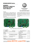
Simplifying System IntegrationTM 73S8024C Demo Board User Manual November 11, 2009 Rev. 1.3 UM_8024C_061 73S8024C Demo Board User Manual UM_8024C_061 © 2009 Teridian Semiconductor Corporation. All rights reserved. Teridian Semiconductor Corporation is a registered trademark of Teridian Semiconductor Corporation. Simplifying System Integration is a trademark of Teridian Semiconductor Corporation. All other trademarks are the property of their respective owners. Teridian Semiconductor Corporation makes no warranty for the use of its products, other than expressly contained in the Company’s warranty detailed in the Teridian Semiconductor Corporation standard Terms and Conditions. The company assumes no responsibility for any errors which may appear in this document, reserves the right to change devices or specifications detailed herein at any time without notice and does not make any commitment to update the information contained herein. Accordingly, the reader is cautioned to verify that this document is current by comparing it to the latest version on http://www.teridian.com or by checking with your sales representative. Teridian Semiconductor Corp., 6440 Oak Canyon, Suite 100, Irvine, CA 92618 TEL (714) 508-8800, FAX (714) 508-8877, http://www.teridian.com 2 Rev. 1.3 UM_8024C_061 73S8024C Demo Board User Manual Table of Contents 1 Introduction ................................................................................................................................... 5 1.1 Package Contents.................................................................................................................... 5 1.2 Safety and ESD Notes ............................................................................................................. 5 2 Basic Connections ........................................................................................................................ 6 3 Hardware Description .................................................................................................................... 7 3.1 Demo Board Connectors, Jumpers and Test Points ................................................................. 7 3.2 Recommended Operating Conditions and Absolute Maximum Ratings ..................................... 9 3.3 73S8024C Pin Description ....................................................................................................... 9 3.4 73S8024C Pinout .................................................................................................................. 11 4 Design Considerations ................................................................................................................ 12 4.1 General Layout Rules ............................................................................................................ 12 4.2 Optimization for Compliance with EMV and NDS.................................................................... 12 5 73S8024C Demo Board Schematics, PCB Layouts and Bill of Materials .................................. 13 5.1 Schematic .............................................................................................................................. 13 5.2 Bill of Materials ...................................................................................................................... 14 5.3 PCB Layouts .......................................................................................................................... 15 6 Ordering Information ................................................................................................................... 18 7 Related Documentation ............................................................................................................... 18 8 Contact Information..................................................................................................................... 18 Revision History .................................................................................................................................. 19 Rev. 1.3 3 73S8024C Demo Board User Manual UM_8024C_061 Figures Figure 1: 73S8024C Demo Board ............................................................................................................ 5 Figure 2: 73S8024C Demo Board Basic Connections .............................................................................. 6 Figure 3: 73S8024C Demo Board Connectors, Jumpers and Test Points ................................................. 8 Figure 4: 73S8024C SO28 Pinout (Top View) ........................................................................................ 11 Figure 5: 73S8024C Demo Board Electrical Schematic .......................................................................... 13 Figure 6: 73S8024C Demo Board Top View........................................................................................... 15 Figure 7: 73S8024C Demo Board Bottom View...................................................................................... 15 Figure 8: 73S8024C Demo Board Top Signal Layer ............................................................................... 16 Figure 9: 73S8024C Demo Board Middle Layer 1, Ground Plane ........................................................... 16 Figure 10: 73S8024C Middle Layer 2, Supply Plane .............................................................................. 17 Figure 11: 73S8024C Demo Board Bottom Signal Layer ........................................................................ 17 Tables Table 1: 73S8024C Demo Board Connector, Jumper and Test Points...................................................... 7 Table 2: Recommended Operating Conditions ......................................................................................... 9 Table 3: Absolute Maximum Ratings ........................................................................................................ 9 Table 4: 73S8024C Card Interface Pins ................................................................................................... 9 Table 5: 73S8024C Miscellaneous Pins ................................................................................................. 10 Table 6: 73S8024C Power and Ground Pins .......................................................................................... 10 Table 7: 72S8024C Microcontroller Interface Pins .................................................................................. 10 Table 8: 73S8024C Demo Board Bill of Materials ................................................................................... 14 Table 9: Order Numbers and Packaging Marks ...................................................................................... 18 4 Rev. 1.3 UM_8024C_061 73S8024C Demo Board User Manual 1 Introduction The 73S8024C Demo Board is a platform for evaluating the Teridian 73S8024C Smart Card Interface device. The board incorporates the 73S8024C integrated circuit and has been designed to operate either as a standalone platform (to be used in conjunction with an external microcontroller) or as a daughter card to be used in conjunction with the 73S1121F evaluation platform. The board has been designed to comply with the EMV 2000 Specification, Version 4.0. 73S8024C Demo Boards can easily be modified to comply with NDS specifications by replacing a few external components that are highlighted in this document. Figure 1: 73S8024C Demo Board 1.1 Package Contents The 73S8024C Demo Board Kit includes: • • 1.2 A 73S8024C Demo Board The following documents on CD: • 73S8024C Data Sheet • 73S8024C Demo Board User Manual (this document) • Application Note Safety and ESD Notes Extreme caution should be taken when handling the 73S8024C Demo Board after connection to live voltages! The 73S8024C Demo Board is ESD sensitive! ESD precautions should be taken when handling this board! Rev. 1.3 5 73S8024C Demo Board User Manual UM_8024C_061 2 Basic Connections The basic connections to the demo board are described below and shown in Figure 2. 1. Connect power supply: Apply 3.3 V to pin 10 of J4. 2. Control signals to the device can be connected through J2 and J4 (see Figure 2 and the Electrical Schematic, Figure 5). 3. To set the clock frequency with an external clock source: • Set JP1 to the SCLK setting. • Apply clock source to pin 1 of J2. • Apply 3.3V (1) or GND (0) to CLKDIV1 and CLKDIV2 pins to set the desired clock rate as follows: CLKDIV1 = CLKDIV2 = 0 clock frequency = SCLK/8 CLKDIV1 = 0, CLKDIV2 =1 clock frequency = SCLK/4 CLKDIV1 = 1, CLKDIV2 =0 clock frequency = SCLK CLKDIV1 = CLKDIV2 = 1 clock frequency = SCLK/2 4. To set the clock frequency using crystal Y1: • The crystal included on the demo board is 12 MHz. • Set JP1 to XTAL position. • Apply 3.3V (1) or GND (0) to CLKDIV1 and CLKDIV2 pins to set the desired clock rate as follows: CLKDIV1 = CLKDIV2 = 0 clock frequency = 1.5 MHz CLKDIV1 = 0, CLKDIV2 =1 clock frequency = 3 MHz CLKDIV1 = 1, CLKDIV2 =0 clock frequency = 12 MHz CLKDIV1 = CLKDIV2 = 1 clock frequency = 6 MHz External clock source. JP1 must be in position SCLK when using an external clock. Otherwise, pin SCLK can be left open. 1 VDD Power Supply: +2.7V to +3.6V (3.3V Typ.) / 50mA SCLK VDD I/OUC AUX1UC GND RSTIN AUX2UC CMDVCC OFF PWRDN 5V/#V CKDIV2 GND CKDIV1 2 VPC Power Supply: Configure JP2 to 3.3V Note: CLKSTOP and CLKLEV can be left NC if unused. 5V/#V too, for 5V cards only. Figure 2: 73S8024C Demo Board Basic Connections 6 Rev. 1.3 UM_8024C_061 73S8024C Demo Board User Manual 3 Hardware Description 3.1 Demo Board Connectors, Jumpers and Test Points Table 1 describes the 73S8024C Demo Board connectors, jumpers and test points. The Item # in Table 1 refers to Figure 3. Table 1: 73S8024C Demo Board Connector, Jumper and Test Points Schematic/ Silkscreen Reference Connectors: 1 J2 Item # 9 J4 16 J5 11 J6 Name 5V Board Supply / Auxiliary Interface 3.3V Board Power / Digital Control Signals Smart Card Connector Smart Card Connector Function 73S8024C auxiliary interface (I/OUC, AUX1UC, AUX2UC), external clock (SCLK) and interrupt (OFF) pins. The external clock (SCLK) can be left open when JP1 is in position XTAL. The 5V power supply is unused and must be left open and JP2 must be inserted in position 3.3V. 3.3V board power supply and the 73S8024C host control signals RSTIN, CMDVCC, 5V/#V, PWRDWN, CLKDIV2 and CLKDIV1. Smart card connector. When inserting a card (credit card size format), contacts must face up. SIM/SAM smart card format connector. J6 is wired in parallel to the smart card connector J5 (underneath the PCB). No SIM/SAM should be inserted when using the credit-card size connector J5. Jumpers: 3 JP1 Clock Selection 17 JP2 VPC Select 2 JP3 VDD Select 8 15 14 JP4 JP5 JP6 – Card Polarity Detect Select Jumper to select between a crystal or an external clock as the frequency reference to the device. The default setting is for a crystal. Jumper to select the value of the power supply for the smart card DC-DC converter (73S8024C input VPC). To support both card voltages, JP2 must be set to position 3.3V. The default setting is 3.3V. Jumper to select the digital voltage which supplies the 73S8024C. Must be set for 3.3V. Not used. The setting of JP5 and JP6 depends on the type of smart card connector used (nominally open or closed) and which 73S8024C card presence switch input is used. The switch is nominally open for the 73S8024C Demo Board. The jumpers can be set to: 1. Use of PRES (default): JP5 set to PRES; JP6 set to VDD. 2. Use of PRES: JP5 set to PREB; JP6 set to GND. Rev. 1.3 7 73S8024C Demo Board User Manual Schematic/ Silkscreen Reference Test Points: 10 TP1 Item # 20 7 12 6 13 5 4 TP2 TP3 TP4 TP5 TP6 TP7 TP8 Name Pin 17 (VDDF_ADJ) Factory Test VCC I/O RST C8 CLK C4 UM_8024C_061 Function VDD voltage fault adjustment. The pin to the left is connected to the VDDF_ADJ pin of the 73S8024C and the pin to the right is GND. When either a resistor R3, or a resistor network R1 and R3 is populated on the board, it adjusts the VDD fault level that internally triggers a card deactivation sequence. By default, the resistors R1 and R3 are not connected. This provides a VDD fault level of 2.3V typical (internally set to the 73S8024C). Refer to the 73S8024C Data Sheet for further information about VDD fault level and determination of the resistor values. Factory test pin. Do not connect. 2-pin test points for each respective smart card signal. The pin label name is the respective signal (i.e. VCC, CLK) and the 2nd pin is GND. Figure 3: 73S8024C Demo Board Connectors, Jumpers and Test Points 8 Rev. 1.3 UM_8024C_061 3.2 73S8024C Demo Board User Manual Recommended Operating Conditions and Absolute Maximum Ratings Table 2 lists the recommended operating conditions and Table 3 lists the absolute maximum ratings. Operation outside these rating limits may cause permanent damage to the device. Table 2: Recommended Operating Conditions Parameter Supply Voltage VDD Supply Voltage VPC Ambient Operating Temperature Input Voltage for Digital Inputs Rating 2.7 to 3.6 VDC 2.7 to 3.6 VDC -40 °C to +85 °C 0 V to VDD + 0.3 V Table 3: Absolute Maximum Ratings Parameter Supply Voltage VDD Supply Voltage VPC Input Voltage for Digital Inputs Storage Temperature Pin Voltage Pin Current ESD Tolerance – Card interface pins ESD Tolerance – Other pins Rating -0.5 to 4.0 VDC -0.5 to 4.0 VDC -0.3 to (VDD+0.5) VDC -60 °C to 150 °C -0.3 to (VDD+0.5) VDC ±100 mA +/- 6 kV +/- 2 kV ESD testing on Card pins is HBM condition, 3 pulses, each polarity referenced to ground. 3.3 73S8024C Pin Description Table 4: 73S8024C Card Interface Pins Rev. 1.3 Name I/O AUX1 AUX2 RST CLK Pin # 11 13 12 14 15 PRES 10 PRES 9 VCC 17 GND 14 Description Card I/O: Data signal to/from card. Includes a pull-up resistor to VCC. AUX1: Auxiliary data signal to/from card. Includes a pull-up resistor to VCC. AUX2: Auxiliary data signal to/from card. Includes a pull-up resistor to VCC. Card reset: provides reset (RST) signal to card. Card clock: provides clock signal (CLK) to card. The rate of this clock is determined by crystal oscillator frequency or external clock input and CLKDIV selections. Card Presence switch: active high indicates card is present. Should be tied to GND when not used, but it includes a high-impedance pull-down resistor. Card Presence switch: active low indicates card is present. Should be tied to VDD when not used, but it includes a high-impedance pull-up resistor. Card power supply: logically controlled by sequencer output of LDO regulator. Requires an external filter capacitor to the card GND. Card ground. 9 73S8024C Demo Board User Manual UM_8024C_061 Table 5: 73S8024C Miscellaneous Pins Name XTALIN Pin # 24 XTALOUT 25 VDDF_ADJ 18 NC 5,7 Description Crystal oscillator input: can either be connected to crystal or driven as a source for the card clock. Crystal oscillator output: connected to crystal. Left open if XTALIN is being used as external clock input. VDD fault threshold adjustment input: this pin can be used to adjust the VDDF values (controls deactivation of the card). Must be left open if unused. Non-connected pin. Table 6: 73S8024C Power and Ground Pins Name VDD VPC GND GND LIN Pin # 21 6 4 22 5 Description System interface supply voltage and supply voltage for internal circuitry. DC-DC converter power supply source. DC-DC converter ground. Digital ground. External inductor. Connect external inductor from pin 2 to VPC. Keep the inductor close to pin 2. Table 7: 72S8024C Microcontroller Interface Pins Name CMDVCC 5V/#V PWRDN CLKDIV1 CLKDIV2 10 Pin # Description 19 Command VCC (negative assertion): Logic low on this pin causes the LDO regulator to ramp the VCC supply to the card and initiates a card activation sequence, if a card is present. 3 5 volt / 3 volt card selection: Logic one selects 5 volts for VCC and card interface, logic low selects 3 volt operation. When the part is to be used with a single card voltage, this pin should be tied to either GND or VDD. However, it includes a high impedance pull-up resistor to default this pin high (selection of 5V card) when not connected. 8 Power Down control input. Active high. When the Power Down mode is set high, all internal analog functions are disabled to place the 73S8024C in its lowest power consumption mode. The Power Down mode is only allowed out of a card session (i.e. when CMDVCC = 1) 1 Sets the divide ratio from the XTAL oscillator (or external clock input) to the card clock. These pins include pull-down resistors. 2 OFF 23 RSTIN I/OUC AUX1UC 20 26 27 AUX2UC 28 CLKDIV1 CLKDIV2 CLOCK RATE 0 0 XTALIN/8 0 1 XTALIN/4 1 1 XTALIN/2 1 0 XTALIN Interrupt signal to the processor. Active low - multi-function indicating fault conditions and/or card presence. Open drain output configuration; includes an internal 22 kΩ pull-up to VDD. Reset Input: This signal is the reset command to the card. System controller data I/O to/from the card. Includes a pull-up resistor to VDD. System controller auxiliary data I/O to/from the card. Includes a pull-up resistor to VDD. System controller auxiliary data I/O to/from the card. Includes a pull-up resistor to VDD. Rev. 1.3 UM_8024C_061 3.4 73S8024C Demo Board User Manual 73S8024C Pinout CLKDIV1 1 28 AUX2UC CLKDIV2 2 27 AUX1UC 5V/#V 3 26 I/OUC GND 4 25 XTALOUT LIN 5 24 XTALIN VPC 6 23 OFF NC 7 22 GND 73S8024C PWRDN 8 21 VDD PRES 9 20 RSTIN PRES 10 19 CMDVCC I/O 11 18 VDDF_ADJ AUX2 12 17 VCC AUX1 13 16 RST GND 14 15 CLK Figure 4: 73S8024C SO28 Pinout (Top View) Rev. 1.3 11 73S8024C Demo Board User Manual UM_8024C_061 4 Design Considerations 4.1 • • • • • • • • 4.2 General Layout Rules Route the auxiliary signals away from card interface signals. Keep the CLK signal as short as possible and with few bends in the trace. Keep the route of the CLK trace to one layer (avoid vias to other plane). Keep the CLK trace away from other traces, especially RST and VCC. Filtering of the CLK trace is allowed for noise purpose. Up to 30 pF to ground is allowed at the CLK pin of the smart card connector. In addition, the zero ohm series resistor, R7, can be replaced for additional filtering (no more than 100 Ω). Keep the VCC trace as short as possible. Make the trace a minimum of 0.5 mm thick. In addition, keep the VCC away from other traces, especially RST and CLK. Keep the trace from L1 to pin 5 of the IC as short as possible. Keep the RST trace away from the VCC and CLK traces. Up to 30 pF to ground is allowed for filtering. Keep the 0.1 µF capacitor close to the VDD pin of the device and directly take the other end to ground. Keep the 0.1 µF capacitor close to the VPC pin of the device and directly take the other end to ground. Keep the 3.3 µF (1.0 µF for NDS) capacitor close to the VCC pin of the smart card connector and directly take other end to ground. Optimization for Compliance with EMV and NDS The default configuration of the demo board contains a 27 pF capacitor (C12) from the CLK pin of the smart connector to ground and a 27 pF capacitor (C13) from the RST pin of the smart connector to ground. These capacitors serve as filters for the CLK and RST signals in the case of long traces or test equipment perturbations. The capacitor on CLK reduces ringing on the trace, reduces coupling to other traces and slows down the edge of the CLK signal. The capacitor on RST helps the perturbation specification in a noisy environment. The filter capacitors can be useful in the EMV test environment and have no effect on NDS testing. C12 and C13 are represented on both the schematic and the BOM. These capacitors are optional filter capacitors on the smart card lines CLK and RST, respectively for each card interface. These capacitors may be adjusted (value not to exceed 30 pF) or removed to optimize performance in each specific application (PCB, card clock frequency, compliance with applicable standards etc). The default VCC capacitor of 3.3 µF is required to meet the dynamic VCC (smart card supply) transient current requirement as specified in the EMV2000 version 4.0 specification. For compliance with NDS, a smaller capacitor of 1 µF is required to meet the activation discharge time specification. 12 Rev. 1.3 UM_8024C_061 73S8024C Demo Board User Manual 5 73S8024C Demo Board Schematics, PCB Layouts and Bill of Materials 5.1 Schematic J1 1 2 3 JP2 5.0V 3.3V SCLK SIO S_C4 S_C8 INT2 GND 1 2 + L1 must be placed close to pin 5 10uF 1 4 12.000MHz PIN18 CLKDIV1 CLKDIV2 5V3V GND_4 LIN VPC NC PWRDN PRES PRES I/O AUX2 AUX1 GND_14 AUX2UC AUX1UC I/OUC XTALOUT XTALIN OFF GND VDD RSTIN CMDVCC VDDF_ADJ VCC RST CLK 28 27 26 25 24 23 22 21 20 19 18 17 16 15 C4 C5 22pF 22pF 3.3V 3.3V VDD R4 0 C8 5.0V 0.1uF 1 2 3 JP3 VDD SELECT 5V JP3 must be set to 3.3V R7 R6 C9 0.47uF 0 73S8024C JP4 1 2 3 R8 Ru R9 Ru C13 27pF HEADER LOCK 3 Resistors not populated C10 + TSM_110_01_L_SV Y1 1 2 R3 0.1uF 1 2 3 4 5 6 7 8 9 10 11 12 13 14 SSM_110_L_SV USR0 USR1 USR2 USR3 USR4 USR5 USR6 USR7 GND 3.3V PGND U1 VDD R5 10uF + C1 L1 10uF J4 TP1 0 C2 TP2 5.0V C3 5V 1 2 3 4 5 6 7 8 9 10 1 2 3 4 5 6 7 8 9 10 Resistors not populated R2 J3 Signal names refer to 73S1121F Evaluation board. R1 5V C1, C2, C8, C9 and L1 must be placed within 5mm of the U1 pins and connected by thick track (wider than 0.5mm) TSM_110_01_L_SV CLKDIV1 CLKDIV2 5V3VB NC PWRDN CMDVCCB RSTIN GND +3.3V VDD VPC SELECT 1 2 3 3.3V JP2 must be set to 3.3V J2 Signal names refer to 73S1121F Evaluation board. XTALIN SELECT XTAL SSM_110_L_SV 1 2 3 4 5 6 7 8 9 10 JP1 SCLK 1 2 3 4 5 6 7 8 9 10 VPC SCLK SIO SC4 SC8 OFFB GND GND GND +5V +5V 10uF R10 Ru Connectors are positioned to allow multiple 8024C boards (stacking) to a 73S1121F evaluation board. Also used for connecting external signals when used as a stand alone board. C11 0.1uF TP3 1 2 TP4 R13 Rd I/O PRESB C8 1 2 3 1 2 VCC 1 2 RST TP7 1 2 1 2 TP3 to TP8 to be placed very close to the pads of J5 CLK TP8 PRES 1 2 CARD DETECT POLARITY SELECT C4 C12 27pF GND 1 2 3 J5 Smart Card Connector SW2 SW1 C7 C6 C5 C3 C2 C1 C8 I/O VPP GND C4 CLK RST VCC Card detection switches are normally open SW-2 SW-1 8 7 6 5 4 3 2 1 VDD 8 7 6 5 4 3 2 1 VDD 10 9 JP6 R12 Rd TP5 TP6 JP5 R11 Rd J6 SIM/SAM Connector Figure 5: 73S8024C Demo Board Electrical Schematic Rev. 1.3 13 73S8024C Demo Board User Manual 5.2 UM_8024C_061 Bill of Materials Table 8 provides the bill of materials for the 73S8024C Demo Board schematic provided in Figure 5. Table 8: 73S8024C Demo Board Bill of Materials 1 Item Quantity 1 2 3 4 5 6 7 3 2 2 1 2 1 5 8 Reference Part PCB Footprint 10 µF 0.1 µF 22 pF 3.3 µF 27 pF 10 µH HEADER 3 1 C1,C3,C10 C2,C8 C4,C5 C11 C12, C13 L1 JP1,JP2,JP3,JP5, JP6 JP4 9 10 2 2 J1,J3 J2,J4 SSM_110_L_SV TSM_110_01_L_SV 11 1 J5 ITT_CCM02-2504 12 13 14 15 16 17 1 3 2 4 4 8 18 1 J6 R2,R4,R7 R5,R6 R1,R8,R9,R10 R3,R11,R12,R13 TP1,TP2,TP3,TP4, TP5,TP6,TP7,TP8 U1 Smart Card Connector SIM/SAM Connector 0 X Ru Rd TP2 19 20 1 2 Y1 C4,C5 Part Number Manufacturer ECJ-2FB0J106M ECJ-1VB1C104K ECJ-1VC1H220J ECJ-2YB0J335K ECJ-0EC1H270J SLF6025 PZC36SAAN Panasonic Panasonic Panasonic Panasonic Panasonic TDK Sullins 22-11-2032 Molex Samtec Samtec ccm02-2504-ND SSM_110_L_SV TSM_110_01_L_S V ccm02-2504 ITT_CCM03-3754 603 603 603 603 2X1_Header CCM03-3754CT-ND P0.0GCT-ND X X X S1011-36-ND CCM03-3754 ERJ-3GEY0R00V X X X PZC36SAAN ITTCannon Panasonic 73S8024C 28SOP X 73S8024C 12.000 MHz 22 pF HC-49US 603 X190-ND ECS-120-20-4DN PCC220ACVCT-ND ECJ-1VC1H220J Teridian Semiconductor ECS Panasonic Header Lock 3 805 603 603 805 402 Digikey Part Number PCC2225CT-ND PCC1762CT-ND PCC220ACVCT-ND PCC1925CT-ND PCC270CQCT-ND X S1011-36-ND 3pins, 2.54 mm pitch 3pins, 2.54 mm WM2701-ND pitch SSM_110_L_SV X TSM_110_01_L_SV X ITTCannon Sullins Ru and Rd are not populated on the board. They can be implemented to adjust the features of the smart card reader. 14 Rev. 1.3 UM_8024C_061 5.3 73S8024C Demo Board User Manual PCB Layouts Figure 6: 73S8024C Demo Board Top View Figure 7: 73S8024C Demo Board Bottom View Rev. 1.3 15 73S8024C Demo Board User Manual UM_8024C_061 Figure 8: 73S8024C Demo Board Top Signal Layer Figure 9: 73S8024C Demo Board Middle Layer 1, Ground Plane 16 Rev. 1.3 UM_8024C_061 73S8024C Demo Board User Manual Figure 10: 73S8024C Middle Layer 2, Supply Plane Figure 11: 73S8024C Demo Board Bottom Signal Layer Rev. 1.3 17 73S8024C Demo Board User Manual UM_8024C_061 6 Ordering Information Table 9 lists the order number used to identify the 73S8024C Demo Board. Table 9: Order Numbers and Packaging Marks Part Description 73S8024C 28-Pin SO Demo Board Order Number 73S8024C-DB 7 Related Documentation The following 73S8024C documents are available from Teridian Semiconductor Corporation: 73S8024C Data Sheet 73S8024C Demo Board User Manual (this document) Teridian 73S8024C versus Philips TDA8024T Application Note 8 Contact Information For more information about Teridian Semiconductor products or to check the availability of the 73S8024C, contact us at: 6440 Oak Canyon Road Suite 100 Irvine, CA 92618-5201 Telephone: (714) 508-8800 FAX: (714) 508-8878 Email: [email protected] For a complete list of worldwide sales offices, go to http://www.teridian.com. 18 Rev. 1.3 UM_8024C_061 73S8024C Demo Board User Manual Revision History Revision 1.0 1.1 1.2 1.3 Rev. 1.3 Date 6/8/2004 8/2/2004 8/23/2005 11/11/2009 Description First publication. Minor corrections. Added new logo. Added Section 1.1, Package Contents. Added Section 1.2, Safety and ESD Notes. Added Section 6, Ordering Information. Added Section 7, Related Documentation. Added Section 8, Contact Information. Miscellaneous editorial changes. 19