1
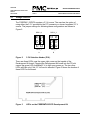
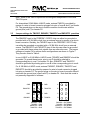
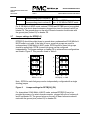
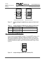
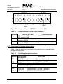
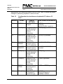
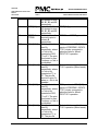
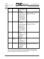
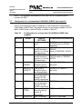
PM2352 FREEDM -32P672 RELEASED DEVELOPMENT KIT BOARD USER MANUAL PMC-2001840 ISSUE 1 DEVELOPMENT KIT BOARD USER MANUAL PM7380 FREEDM -32P672 DEVELOPMENT KIT USER MANUAL RELEASED ISSUE 1: DECEMBER 2000 PROPRIETARY AND CONFIDENTIAL TO PMC-SIERRA, INC., AND FOR ITS CUSTOMERS’ INTERNAL USE PM2352 FREEDM -32P672 RELEASED DEVELOPMENT KIT BOARD USER MANUAL PMC-2001840 ISSUE 1 DEVELOPMENT KIT BOARD USER MANUAL CONTENTS 1 OVERVIEW.............................................................................................. 1 1.1 2 FEATURES ................................................................................... 1 HARDWARE CONFIGURATION ............................................................. 2 2.1 VOLTAGE SELECTION ................................................................ 4 2.2 SYSCLK JUMPER SETTING ........................................................ 5 2.3 JUMPER SETTING FOR RMVCK[3:0] PROVISION..................... 5 2.4 JUMPER SETTING FOR TMVCK[3:0] PROVISION ..................... 6 2.5 JUMPER SETTINGS FOR TMV8DC, RMV8DC, TMV8FPC AND RMV8FPC PROVISION ............................................................... 8 2.6 JUMPER SETTINGS FOR TFP8B AND RFP8B ........................... 9 2.7 JUMPER SETTINGS FOR RFPB[3:0]......................................... 10 2.8 JUMPER SETTINGS FOR TFPB[3:0] ..........................................11 2.9 JUMPER SETTINGS FOR SELECTION OF RCLK[2:0] AND TCLK[2:0] .................................................................................... 12 2.10 JUMPER SETTINGS FOR ENABLING OF RCLK[15:0] ............. 13 2.11 JUMPER SETTINGS FOR ENABLING OF RCLK[31:16] ........... 15 2.12 JUMPER SETTINGS FOR ENABLING OF TCLK[15:0] .............. 17 2.13 JUMPER SETTINGS FOR ENABLING OF TCLK[31:16] ............ 18 2.14 JUMPER SETTINGS FOR DATA LOOPBACK ON LINKS 2 THROUGH 31 ............................................................................. 20 2.15 JUMPER SETTINGS FOR DATA LOOPBACK/CROSS-CONNECT ON LINKS 0 AND 1 ..................................................................... 21 2.16 JUMPER SETTINGS FOR BERT EMULATION .......................... 22 2.17 PLACEMENT OF OSCILLATORS IN THE SOCKETS................ 23 PROPRIETARY AND CONFIDENTIAL TO PMC-SIERRA, INC., AND FOR ITS CUSTOMERS’ INTERNAL USE i PM2352 FREEDM -32P672 RELEASED DEVELOPMENT KIT BOARD USER MANUAL PMC-2001840 3 4 ISSUE 1 DEVELOPMENT KIT BOARD USER MANUAL CONFIGURATIONS FOR THE TEST CASES ....................................... 25 3.1 CONFIGURATION FOR PCI INTERFACE TEST........................ 25 3.2 CONFIGURATION FOR UNCHANNELIZED T1 LOOPBACK MODE.......................................................................................... 26 3.3 CONFIGURATION FOR UNCHANNELIZED E1 LOOPBACK MODE.......................................................................................... 28 3.4 CONFIGURATION FOR 16 T1/ 16 E1 UNCHANNELIZED LOOPBACK MODE..................................................................... 31 3.5 CONFIGURATION FOR UNCHANNELIZED 52 MBIT/S............. 33 3.6 CONFIGURATION FOR UNCHANNELIZED MIXED DS3/T1/E1 DATA LOOPBACK....................................................................... 35 3.7 CONFIGURATION FOR UNCHANNELIZED 2.048 MBIT/S H-MVIP DATA LOOPBACK....................................................................... 38 3.8 CONFIGURATION FOR UNCHANNELIZED 8.192 MBIT/S H-MVIP DATA LOOPBACK....................................................................... 40 3.9 BERT SIGNAL VERIFICATION ................................................... 41 HOW TO PROCEED WITH THE TEST CASES .................................... 44 PROPRIETARY AND CONFIDENTIAL TO PMC-SIERRA, INC., AND FOR ITS CUSTOMERS’ INTERNAL USE ii PM2352 FREEDM -32P672 RELEASED DEVELOPMENT KIT BOARD USER MANUAL PMC-2001840 ISSUE 1 DEVELOPMENT KIT BOARD USER MANUAL LIST OF FIGURES FIGURE 1 FREEDM-32P672 DEVELOPMENT KIT BOARD DIAGRAM ....... 3 FIGURE 2 3.3V SELECTION HEADER (P16)................................................... 4 FIGURE 3 LEDS ON THE FREEDM-32P672 DEVELOPMENT KIT.............. 4 FIGURE 4 JUMPER SETTING FOR SYSCLK (P3) .......................................... 5 FIGURE 5 JUMPER SETTINGS FOR RMVCK[3:0] (P5). ................................. 6 FIGURE 6 JUMPER SETTING FOR TMVCK[3:0] (P6). .................................... 7 FIGURE 7 JUMPER SETTINGS FOR ENABLING OF RMV8FPC, TMV8FPC, TMV8DC, AND RMV8DC (P4)............................................................................ 9 FIGURE 8 JUMPER SETTINGS FOR RFP8B AND TFP8B (P9) ...................... 9 FIGURE 9 JUMPER SETTINGS FOR RFPB[3:0] (P8) ................................... 10 FIGURE 10JUMPER SETTINGS FOR TFPB[3:0] (P1).....................................11 FIGURE 11 JUMPER SETTINGS FOR SELECTION OF RCLK[2:0] AND TCLK[2:0] (P7).................................................................................................. 13 FIGURE 12JUMPER SETTINGS FOR ENABLING OF RCLK[15:0] (P12) ...... 14 FIGURE 13JUMPER SETTINGS FOR ENABLING OF RCLK[31:16] (P11)..... 16 FIGURE 14JUMPER SETTINGS FOR ENABLING OF TCLK[15:0] (P13)....... 17 FIGURE 15JUMPER SETTINGS FOR TCLK[31:16] (P14).............................. 19 FIGURE 16JUMPER SETTINGS FOR DATA LOOPBACK ON LINKS 2 TO 3121 FIGURE 17JUMPER SETTINGS FOR LOOPBACK/CROSS-CONNECT ON LINKS 0 AND 1 (P2) ......................................................................................... 22 FIGURE 18JUMPER SETTINGS FOR BERT DATA EMULATION (P15) ......... 22 FIGURE 19JUMPER SETTINGS FOR BERT CLOCK EMULATION (P7)........ 23 PROPRIETARY AND CONFIDENTIAL TO PMC-SIERRA, INC., AND FOR ITS CUSTOMERS’ INTERNAL USE iii PM2352 FREEDM -32P672 RELEASED DEVELOPMENT KIT BOARD USER MANUAL PMC-2001840 ISSUE 1 DEVELOPMENT KIT BOARD USER MANUAL LIST OF TABLES TABLE 1 JUMPER SETTING FOR SYSCLK .................................................. 5 TABLE 2 JUMPER SETTINGS FOR RMVCK[3:0].......................................... 6 TABLE 3 JUMPER SETTING FOR TMVCK[3:0]............................................. 7 TABLE 4 JUMPER SETTINGS FOR ENABLING OF RMV8FPC, TMV8FPC, TMV8DC, AND RMV8DC.................................................................................... 9 TABLE 5 JUMPER SETTINGS FOR RFP8B AND TFP8B.............................. 9 TABLE 6 JUMPER SETTINGS FOR RFPB[3:0] ............................................11 TABLE 7 JUMPER SETTINGS FOR TFPB[3:0].............................................11 TABLE 8 JUMPER SETTINGS FOR SELECTION OF RCLK[2:0] AND TCLK[2:0] …………………………………………………………………………….13 TABLE 9 JUMPER SETTINGS FOR ENABLING OF RCLK[15:0] ................ 14 TABLE 10 JUMPER SETTINGS FOR ENABLING OF RCLK[31:16] .............. 15 TABLE 11 JUMPER SETTINGS FOR TCLK[15:0].......................................... 18 TABLE 12 JUMPER SETTINGS FOR ENABLING TCLK[31:16]..................... 18 TABLE 13 JUMPER SETTINGS FOR DATA LOOPBACK ON LINKS 2 THROUGH 31................................................................................................... 20 TABLE 14 JUMPER SETTINGS FOR LOOPBACK/CROSS-CONNECT ON LINKS 0 AND 1 ................................................................................................. 22 TABLE 15 JUMPER SETTINGS FOR BERT CLOCK EMULATION ............... 23 TABLE 16 OSCILLATOR PLACEMENT IN SOCKETS ................................... 23 TABLE 17 CONFIGURATION FOR THE PCI INTERFACE TEST .................. 25 TABLE 18 CONFIGURATION FOR SIMULTANEOUS LOOPBACK OF E1 DATA ON 32 LINKS .................................................................................................... 29 TABLE 19 CONFIGURATION FOR 16 T1/E1 UNCHANNELIZED LOOPBACK 31 PROPRIETARY AND CONFIDENTIAL TO PMC-SIERRA, INC., AND FOR ITS CUSTOMERS’ INTERNAL USE iv PM2352 FREEDM -32P672 RELEASED DEVELOPMENT KIT BOARD USER MANUAL PMC-2001840 ISSUE 1 DEVELOPMENT KIT BOARD USER MANUAL TABLE 20 SIMULTANEOUS LOOPBACK OF UNCHANNELIZED 52 MBIT/S DATA ON LINKS 0 THROUGH 2 ...................................................................... 33 TABLE 21 SIMULTANEOUS LOOPBACK OF UNCHANNELIZED MIXED DS3/T1/E1 DATA .............................................................................................. 35 TABLE 22 CONFIGURATION FOR UNCHANNELIZED 2.048 MBIT/S H-MVIP DATA LOOPBACK ............................................................................................ 38 TABLE 23 CONFIGURATION FOR UNCHANNELIZED 8.192 MBIT/S H-MVIP DATA LOOPBACK ............................................................................................ 40 TABLE 24 CONFIGURATION FOR BERT SIGNAL VERIFICATION TEST .... 42 PROPRIETARY AND CONFIDENTIAL TO PMC-SIERRA, INC., AND FOR ITS CUSTOMERS’ INTERNAL USE v PM2352 FREEDM -32P672 RELEASED DEVELOPMENT KIT BOARD USER MANUAL PMC-2001840 1 ISSUE 1 DEVELOPMENT KIT BOARD USER MANUAL OVERVIEW The FREEDM-32P672 Development Kit consists of an add-on PCI card that can be used to test the functionality of the FREEDM-32P672 chip. The PCI card consists of all the necessary components used for testing the various functions of the FREEDM-32P672 device. This document provides the necessary information for configuring the FREEDM-32P672 Development Kit Board Rev 2.0. jumper settings. 1.1 Features • The Development Kit supports a 33/66 MHz, 32 bit Peripheral Component Interconnect (PCI) 2.1 compliant bus for configuration, monitoring and transfer of packet data. • The Development Kit supports both unchannelized H-MVIP as well as nonH-MVIP traffic. Channelized T1/E1 traffic on the 32 links is not directly supported since there is no provision for gapping of the link clocks. Channelized H-MVIP mode is not directly supported since the frame pulses are not generated on the Development Kit card. • Channelized T1/E1 operation can be supported only with an external gapped clock (i.e. gapped clock from an external source). Channelized H-MVIP mode can be supported with external frame pulses and frame pulse clocks. PROPRIETARY AND CONFIDENTIAL TO PMC-SIERRA, INC., AND FOR ITS CUSTOMERS’ INTERNAL USE 1 PM2352 FREEDM -32P672 RELEASED DEVELOPMENT KIT BOARD USER MANUAL PMC-2001840 2 ISSUE 1 DEVELOPMENT KIT BOARD USER MANUAL HARDWARE CONFIGURATION Jumper settings are used to configure the Development Kit board for various modes of operation. The supported modes include: • Unchannelized T1 mode • Unchannelized E1 mode • Unchannelized 52 MHz mode • Unchannelized 2.048 Mbit/s H-MVIP mode • Mixed mode For non-H-MVIP modes, only the following configurations can be achieved using jumper settings: • 32 T1 links • 32 E1 links • 16 T1 links and 16 E1 links • 3 DS-3/unchannelized 52 Mbit/s links • Mixed mode – 1 DS-3 link and T1/E1 links With external gapped clock/frame pulse signals, channelized non H-MVIP as well as H-MVIP mode can be supported. This includes channelized 8 Mbit/s H-MVIP mode, for which an external frame pulse as well as frame pulse clocks are required. Note that the supplied software does not include support for includes channelized 8 Mbit/s H-MVIP mode. This section gives a detailed description of the jumper settings on the various headers. Figure 1 represents the block diagram for the FREEDM-32P672 development kit board. PROPRIETARY AND CONFIDENTIAL TO PMC-SIERRA, INC., AND FOR ITS CUSTOMERS’ INTERNAL USE 2 PM2352 FREEDM -32P672 RELEASED DEVELOPMENT KIT BOARD USER MANUAL PMC-2001840 Figure 1 ISSUE 1 DEVELOPMENT KIT BOARD USER MANUAL FREEDM -32P672 Development Kit Board Diagram PROPRIETARY AND CONFIDENTIAL TO PMC-SIERRA, INC., AND FOR ITS CUSTOMERS’ INTERNAL USE 3 PM2352 FREEDM -32P672 RELEASED DEVELOPMENT KIT BOARD USER MANUAL PMC-2001840 2.1 ISSUE 1 DEVELOPMENT KIT BOARD USER MANUAL Voltage Selection The FREEDM-32P672 requires a 3.3 V source. The user has the option of using either the 3.3 V provided by the PCI connector or a board regulated 3.3 V source. The jumper settings for achieving these configurations are shown in Figure 2. Figure 2 REG 3_3 REG 3_3 PCI 3_3 PCI 3_3 A B 3.3V Selection Header (P16). There are three LED’s near the upper right corner on the topside of the Development Kit board. Plugging the Development Kit board into the PCI slot causes the green LED (indicating 5 V) to light upon power up. The two other LED’s will light only if the 3.3 V source is selected. Figure 3 shows the location of these LED’s on the board. Figure 3 LED’s on the FREEDM -32P672 Development Kit PROPRIETARY AND CONFIDENTIAL TO PMC-SIERRA, INC., AND FOR ITS CUSTOMERS’ INTERNAL USE 4 PM2352 FREEDM -32P672 RELEASED DEVELOPMENT KIT BOARD USER MANUAL PMC-2001840 2.2 ISSUE 1 DEVELOPMENT KIT BOARD USER MANUAL SYSCLK Jumper Setting The SYSCLK input of the FREEDM-32P672 chip can be provided with either a 40 MHz clock from an oscillator, or the PCICLKO clock output of the FREEDM32P672 chip (provided that a 33 MHz PCI bus is in use). The jumper settings on header P3 to achieve these configurations are shown in Figure 4. The jumper settings are also listed in Table 1. A B C SYSCLK <= 40 MHz A B C SYSCLK <= PCICLKO Figure 4 Jumper setting for SYSCLK (P3) Table 1 Jumper setting for SYSCLK HEADER JUMPER SETTING CONFIGURATION P3 Shorting jumper over pins A and B SYSCLK from oscillator P3 Shorting jumper over pins B and C SYSCLK from PCICLKO Note: Pins B and C should only be shorted when the card is installed in a system with a 33 MHz PCI bus. 2.3 Jumper setting for RMVCK[3:0] provision Each of the four RMVCK inputs to the FREEDM-32P672 chip can be configured independently. Each RMVCK input to the FREEDM-32P672 chip can either be grounded or provided with a 4.096 MHz clock from an oscillator. The jumper settings on header P5 to achieve these configurations are as shown in Figure 5. The jumper settings are also listed in Table 2. In non-H-MVIP or 8.192 Mbit/s H-MVIP mode, RMVCK[3:0] should be grounded. To ground RMVCK[n] (0 ≤ n ≤ 3), pin B-n should be shorted to pin C-n on header P5. 4.096 MHz clock from an oscillator can be provided to RMVCK[n] by shorting pins B-n and A-n. The jumper settings in Figure 5 (a) correspond to 4.096 MHz on RMVCK[3:0], whereas the jumper settings in Figure 5(b) correspond to grounded RMVCK[3:0]. PROPRIETARY AND CONFIDENTIAL TO PMC-SIERRA, INC., AND FOR ITS CUSTOMERS’ INTERNAL USE 5 PM2352 FREEDM -32P672 RELEASED DEVELOPMENT KIT BOARD USER MANUAL PMC-2001840 3 ISSUE 1 2 1 DEVELOPMENT KIT BOARD USER MANUAL 0 3 2 1 0 A A B B C C RMVCK[3:0] <= 4.096 MHz RMVCK[3:0] <= GND Note : Numbers written above the header represent the link groups. Figure 5 Jumper settings for RMVCK[3:0] (P5). Table 2 Jumper settings for RMVCK[3:0] HEADER JUMPER SETTINGS P5 Shorting jumper over pins A-n and B-n (0 ≤ n ≤ 3) CONFIGURATION 4.096 MHz input to RMVCK[n]. (0 ≤ n ≤ 3) Unchannelized 2.048 Mbit/s HMVIP mode . P5 Shorting jumper over pins C-n and B-n (0 ≤ n ≤ 3) RMVCK[n] grounded. (0 ≤ n ≤ 3) Non – 2.048 Mbit/s H-MVIP mode. Note : Each of the RMVCK inputs can be configured independent of the other RMVCK inputs. For channelized 2.048 Mbit/s H-MVIP mode, external RMVCK should be provided by means of a wire to board connector plugged into pins of rows B and C on header P5. The ground plugs on the wire to board connector should mate with the ground pins (row C) on header P5. 2.4 Jumper setting for TMVCK[3:0] provision Similar to RMVCK, each of the four TMVCK inputs to the FREEDM-32P672 device can be configured independently. Each TMVCK input to the FREEDM- PROPRIETARY AND CONFIDENTIAL TO PMC-SIERRA, INC., AND FOR ITS CUSTOMERS’ INTERNAL USE 6 PM2352 FREEDM -32P672 RELEASED DEVELOPMENT KIT BOARD USER MANUAL PMC-2001840 ISSUE 1 DEVELOPMENT KIT BOARD USER MANUAL 32P672 device can either be grounded or provided with a 4.096 MHz clock from an oscillator. The jumper settings on header P6 to achieve these configurations are shown in Figure 6. The jumper settings are also listed in Table 3. In non-H-MVIP or 8.192 Mbit/s H-MVIP mode, TMVCK[3:0] should be grounded. To ground TMVCK[n] (0 ≤ n ≤ 3), pin B-n should be shorted to pin C-n on header P6. The 4.096 MHz clock from an oscillator can be provided to TMVCK[n] by shorting pins B-n and A-n. The jumper settings in Figure 6(a) correspond to 4.096 MHz on TMVCK[3:0], whereas the jumper settings in Figure 6(b) correspond to grounded TMVCK[3:0]. 0 1 2 3 0 1 2 3 A A B B C C TMVCK[3:0] <= 4.096 MHz TMVCK[3:0] <= GND Note : Numbers written above the header represent the link groups. Figure 6 Jumper setting for TMVCK[3:0] (P6). Table 3 Jumper setting for TMVCK[3:0] HEADER JUMPER SETTINGS P6 Shorting jumper over pins A-n and B-n (0 ≤ n ≤ 3) CONFIGURATION 4.096 MHz input to TMVCK[n]. (0 ≤ n ≤ 3) Unchannelized 2.048 Mbit/s HMVIP mode . P6 Shorting jumper over pins C-n and B-n (0 ≤ n ≤ 3) TMVCK[n] grounded. (0 ≤ n ≤ 3) Non – 2.048 Mbit/s H-MVIP mode. PROPRIETARY AND CONFIDENTIAL TO PMC-SIERRA, INC., AND FOR ITS CUSTOMERS’ INTERNAL USE 7 PM2352 FREEDM -32P672 RELEASED DEVELOPMENT KIT BOARD USER MANUAL PMC-2001840 ISSUE 1 DEVELOPMENT KIT BOARD USER MANUAL Note : Each of the TMVCK inputs can be configured independent of the other TMVCK inputs. For channelized 2.048 Mbit/s H-MVIP mode, external TMVCK is provided by means of a wire to board connector plugged into pins of rows B and C on header P6. The ground plugs on the wire to board connector should mate with the ground pins (row C) on header P6. 2.5 Jumper settings for TMV8DC, RMV8DC, TMV8FPC and RMV8FPC provision The RMV8DC input to the FREEDM-32P672 chip can either be grounded or provided with a 16.384 MHz clock from an external source by means of a wire to board connector. Similarly, the TMV8DC input to the FREEDM-32P672 chip can either be grounded or provided with a 16.384 MHz clock from an external source. The RMV8FPC and TMV8FPC pins of the chip can either be grounded or provided with frame pulse clock signals from an external source. The jumper settings on header P4 to achieve these configurations are shown in Figure 7. They are also listed in Table 4. In non-H-MVIP or 2.048 Mbit/s H-MVIP mode, TMV8DC and RMV8DC should be grounded. To ground these inputs, pins in row D should be shorted to corresponding pins in row C on header P4. Also, RMV8FPC and TMV8FPC should be grounded by shorting pins in row B to the corresponding pins in row A. For 8.192 Mbit/s H-MVIP mode, external TMV8DC, RMV8DC, TMV8FPC and RMV8FPC should be provided by means of a wire to board connector plugged into pins on header P4. The ground plugs on the wire to board connector should mate with the ground pins (rows A and C) on header P4. Note that this mode is not presently supported in software. GND RMV8FPC GND RMV8DC A GND A B TMV8FPC B C GND C D D RMV8DC = GND TMV8DC = GND RMV8FPC = GND TMV8FPC = GND TMV8DC RMV8DC = EXTERNAL TMV8DC = EXTERNAL RMV8FPC = EXTERNAL TMV8FPC = EXTERNAL PROPRIETARY AND CONFIDENTIAL TO PMC-SIERRA, INC., AND FOR ITS CUSTOMERS’ INTERNAL USE 8 PM2352 FREEDM -32P672 RELEASED DEVELOPMENT KIT BOARD USER MANUAL PMC-2001840 ISSUE 1 DEVELOPMENT KIT BOARD USER MANUAL Figure 7 Jumper settings for enabling of RMV8FPC, TMV8FPC, TMV8DC, and RMV8DC (P4) Table 4 Jumper settings for enabling of RMV8FPC, TMV8FPC, TMV8DC, and RMV8DC HEADER P4 JUMPER SETTING Pins in row A shorted to corresponding pins in row B Pins in row C shorted to corresponding pins in row D P4 Wire to board connector plugged into pins on header P4. CONFIGURATION TMV8DC and RMV8DC grounded. TMV8FPC and RMV8FPC grounded. Non-8.192 Mbit/s H-MVIP mode. 16.384 MHz clock provided to RMV8DC and TMV8DC. 4.096 MHz clock provided to RMV8FPC and TMV8FPC. Note : The falling edges of RMV8FPC and TMV8FPC should be aligned respectively with the falling edges of RMV8DC and TMV8DC, with no more than 10 ns skew. 2.6 Jumper settings for TFP8B and RFP8B TFP8B and RFP8B should be pulled down to ground when unchannelized 8.192 Mbit/s H-MVIP mode is not used. Both TFP8B and RFP8B should be pulled high for unchannelized 8.192 Mbit/s H-MVIP mode. The jumper settings on header P9 to achieve this configuration are shown in Figure 8. They are also listed in Table 5. TFP8B RFP8B B C A RFP8B <= GND TFP8B <= GND Non-8.192 Mbit/s H-MVIP Mode B C A RFP8B <= 3.3V TFP8B <= 3.3V Unchannelized 8.192 Mbit/s H-MVIP Mode Figure 8 Jumper settings for RFP8B and TFP8B (P9) Table 5 Jumper settings for RFP8B and TFP8B HEADER P9 JUMPER SETTING Pins in column C shorted to CONFIGURATION TFP8B and RFP8B pulled high PROPRIETARY AND CONFIDENTIAL TO PMC-SIERRA, INC., AND FOR ITS CUSTOMERS’ INTERNAL USE 9 PM2352 FREEDM -32P672 RELEASED DEVELOPMENT KIT BOARD USER MANUAL PMC-2001840 P9 ISSUE 1 DEVELOPMENT KIT BOARD USER MANUAL corresponding pins in column B Pins in column A shorted to corresponding pins in column B (3.3 V). TFP8B and RFP8B grounded. Non - 8.192 Mbit/s H-MVIP mode. For 8.192 Mbit/s H-MVIP mode, external TFP8B and RFP8B have to be provided by means of a wire to board connector plugged into pins of columns A and B on header P9. The ground plugs on the wire to board connector should mate with the ground pins (column A) on header P9. 2.7 Jumper settings for RFPB[3:0] RFPB[3:0] should be pulled down to ground when unchannelized 2.048 Mbit/s HMVIP mode is not used. If the links in one or more link groups are used for unchannelized 2.048 Mbit/s H-MVIP mode, RFPB inputs for these link groups should be pulled high. RFPB for each link group can be configured independently. The jumper settings on header P8 to achieve these configurations are listed in Figure 9. They are also listed in Table 6. 0 0 1 1 2 2 3 3 C B A RFPB <= 3.3V C B A RFPB[3:0] <= GND Note : RFPB for each link group can be independently configured with a single shorting jumper. Figure 9 Jumper settings for RFPB[3:0] (P8) For channelized 2.048 Mbit/s H-MVIP mode, external RFPB[3:0] has to be provided by means of a wire to board connector plugged into pins of columns A and B on header P8. The ground plugs on the wire to board connector should mate with the ground pins (column A) on header P8. PROPRIETARY AND CONFIDENTIAL TO PMC-SIERRA, INC., AND FOR ITS CUSTOMERS’ INTERNAL USE 10 PM2352 FREEDM -32P672 RELEASED DEVELOPMENT KIT BOARD USER MANUAL PMC-2001840 Table 6 2.8 ISSUE 1 DEVELOPMENT KIT BOARD USER MANUAL Jumper settings for RFPB[3:0] HEADER P8 JUMPER SETTINGS Pin A-n shorted to pin B-n (0 ≤ n ≤ 3) P8 Pin C-n shorted to pin B-n (0 ≤ n ≤ 3) CONFIGURATION RFPB[n] grounded. (0 ≤ n ≤ 3) Non- 2.048 Mbit/s H-MVIP mode. RFPB[n] pulled high (3.3 V). (0 ≤ n ≤ 3) Unchannelized 2.048 Mbit/s H-MVIP mode on link group n. Jumper settings for TFPB[3:0] TFPB[3:0] should be pulled down to ground when unchannelized 2.048 Mbit/s HMVIP mode is not used. If the links in one or more link groups are used for unchannelized 2.048 Mbit/s H-MVIP mode, the TFPB inputs for these link groups should be pulled high. TFPB for each link group can be configured independently. The jumper settings on header P1 to achieve these configurations are listed in Figure 10. They are also listed in Table 7. 0 1 2 3 0 1 2 3 A A B B C C TFPB[3:0] <= GND TFPB[3:0] <= 3.3V Note : TFPB for each link group can be independently configured with a single shorting jumper. Figure 10 Jumper settings for TFPB[3:0] (P1) Table 7 Jumper settings for TFPB[3:0] HEADER P1 P1 JUMPER SETTINGS Pin A-n shorted to pin B-n (0 ≤ n ≤ 3) Pin C-n shorted to CONFIGURATION TFPB[n] grounded . (0 ≤ n ≤ 3) Non- 2.048 Mbit/s H-MVIP mode. TFPB[n] pulled high (3.3 V). PROPRIETARY AND CONFIDENTIAL TO PMC-SIERRA, INC., AND FOR ITS CUSTOMERS’ INTERNAL USE 11 PM2352 FREEDM -32P672 RELEASED DEVELOPMENT KIT BOARD USER MANUAL PMC-2001840 HEADER ISSUE 1 DEVELOPMENT KIT BOARD USER MANUAL JUMPER SETTINGS pin B-n (0 ≤ n ≤ 3) CONFIGURATION (0 ≤ n ≤ 3) Unchannelized 2.048 Mbit/s H-MVIP mode on link group n. For channelized 2.048 Mbit/s H-MVIP mode, external TFPB[3:0] has to be provided by means of a wire to board connector plugged into pins of rows A and B on header P1. The ground plugs on the wire to board connector should mate with the ground pins (row A) on header P1. 2.9 Jumper settings for selection of RCLK[2:0] and TCLK[2:0] In non-H-MVIP mode, RCLK[2:0] and TCLK[2:0] can be set to either T1/E1 clock frequency or DS-3/52 MHz clock frequency. Jumper settings on header P7 to make this selection are listed in Table 8. Figure 11 shows how the jumpers are used on header P7. RCL52(0-2) TCL52(0-2) C B A R0 R1 R2 T0 T2 T1 TBCLK RBCLK A) T1/E1 Frequency on RCLK[2:0] and TCLK[2:0] RCL52(0-2) TCL52(0-2) C B A R0 R1 R2 T0 T2 T1 RBCLK TBCLK B) DS-3/52 MHz Frequency on RCLK[2:0] and TCLK[2:0] PROPRIETARY AND CONFIDENTIAL TO PMC-SIERRA, INC., AND FOR ITS CUSTOMERS’ INTERNAL USE 12 PM2352 FREEDM -32P672 RELEASED DEVELOPMENT KIT BOARD USER MANUAL PMC-2001840 Figure 11 ISSUE 1 DEVELOPMENT KIT BOARD USER MANUAL Jumper settings for selection of RCLK[2:0] and TCLK[2:0] (P7) Note : The numbers T0, T1 and T2, corresponding to TCL52 (0-2) and R0, R1 and R2, corresponding to RCL52 (0-2), shown in Figure 11, respectively represent transmit and receive links 0, 1 and 2. Table 8 HEADER P7 P7 P7 P7 Jumper settings for selection of RCLK[2:0] and TCLK[2:0] JUMPER SETTINGS Pin A-Rn shorted to pin B-Rn (0 ≤ n ≤ 2) under RCL52 (0-2) label Pin C-Rn shorted to pin B-Rn (0 ≤ n ≤ 2) under RCL52 (0-2) label Pin A-Tn shorted to pin B-Tn (0 ≤ n ≤ 2) under TCL52 (0-2) label Pin C-Tn shorted to pin B-Tn (0 ≤ n ≤ 2) under TCL52 (0-2) label CONFIGURATION DS-3/52 MHz frequency on RCLK[2:0] T1/E1 frequency on RCLK[2:0] DS-3/52 MHz frequency on TCLK[2:0] T1/E1 frequency on TCLK[2:0] Note : Each RCLK or TCLK selection can be configured independently. 2.10 Jumper settings for enabling of RCLK[15:0] RCLK[15:0] should be grounded when unchannelized H-MVIP mode is used on links 0 through 15. If one or more links from 0 through 15 is used for receiving non-H-MVIP traffic, the corresponding receive link clocks (i.e. RCLK[n] where 0 ≤ n ≤ 15 ) should be enabled. The jumper settings on header P12 for enabling RCLK[15:0] are listed in Table 9. Figure 12 shows the jumper settings for enabling all 16 receive link clocks from RCLK[15] through RCLK[0]. PROPRIETARY AND CONFIDENTIAL TO PMC-SIERRA, INC., AND FOR ITS CUSTOMERS’ INTERNAL USE 13 PM2352 FREEDM -32P672 RELEASED DEVELOPMENT KIT BOARD USER MANUAL PMC-2001840 A ISSUE 1 B DEVELOPMENT KIT BOARD USER MANUAL 0 0 1 1 2 2 3 3 4 4 5 5 6 6 7 7 13 13 10 10 15 15 14 14 12 12 11 11 8 8 9 9 C RCLK[2:0] <= T1/E1/DS-3/52 MHz RCLK[15:3] <= T1/E1 RCLK[15:0] enabled (non H-MVIP Mode) A B C RCLK[15:0] <= GND RCLK[15:0] grounded (H-MVIP Mode) Note : The pins for links from 0 through 15 are not in sequential order. Each of the RCLK inputs to FREEDM-32P672 chip can be independently enabled. Figure 12 Jumper settings for enabling of RCLK[15:0] (P12) Table 9 Jumper settings for enabling of RCLK[15:0] HEADER P12 JUMPER SETTING Pin A-n shorted to pin B-n (0 ≤ n ≤ 15) P12 Pin C-n shorted to pin B-n (0 ≤ n ≤ 15) CONFIGURATION RCLK[n] connected to FREEDM-32P672 (0 ≤ n ≤ 15) RCLK[n] grounded (0 ≤ n ≤ 15) PROPRIETARY AND CONFIDENTIAL TO PMC-SIERRA, INC., AND FOR ITS CUSTOMERS’ INTERNAL USE 14 PM2352 FREEDM -32P672 RELEASED DEVELOPMENT KIT BOARD USER MANUAL PMC-2001840 ISSUE 1 DEVELOPMENT KIT BOARD USER MANUAL For channelized non-H-MVIP mode, externally gapped RCLK[15:0] should be provided by means of a wire to board connector plugged into pins of rows B and C on header P12. The ground plugs on the wire to board connector should mate with the ground pins (row C) on header P12. 2.11 Jumper settings for enabling of RCLK[31:16] RCLK[31:16] should be grounded when unchannelized H-MVIP mode is used on links 16 through 31. If one or more links from 16 through 31 are used for receiving non-H-MVIP traffic, the corresponding receive link clocks (i.e. RCLK[n] where 16 ≤ n ≤ 31 ) should be enabled. The jumper settings on header P11 for enabling RCLK[31:16] are listed in Table 10. Figure 13 shows the jumper settings for enabling all 16 receive link clocks from RCLK[31] through RCLK[16]. Table 10 Jumper settings for enabling of RCLK[31:16] HEADER JUMPER SETTING P11 Pin A-n shorted to pin B-n (16 ≤ n ≤ 31) P11 Pin C-n shorted to pin B-n (16 ≤ n ≤ 31) CONFIGURATION RCLK[n] connected to FREEDM32P672 (16 ≤ n ≤ 31) RCLK[n] grounded (16 ≤ n ≤ 31) For channelized non-H-MVIP mode, externally gapped RCLK[31:16] should be provided by means of a wire to board connector plugged into pins of rows B and C on header P11. The ground plugs on the wire to board connector should mate with the ground pins (row C) on header P11. PROPRIETARY AND CONFIDENTIAL TO PMC-SIERRA, INC., AND FOR ITS CUSTOMERS’ INTERNAL USE 15 PM2352 FREEDM -32P672 RELEASED DEVELOPMENT KIT BOARD USER MANUAL PMC-2001840 A ISSUE 1 B DEVELOPMENT KIT BOARD USER MANUAL 16 16 17 17 18 18 19 19 20 20 21 21 22 22 23 23 24 24 25 25 26 26 27 27 28 28 29 29 30 30 31 31 C RCLK[31:16] <= T1/E1 Non H-MVIP Mode A B C RCLK[31:16] grounded (H-MVIP Mode) Note : Each of the RCLK inputs to FREEDM-32P672 chip can be independently enabled. Figure 13 Jumper settings for enabling of RCLK[31:16] (P11) PROPRIETARY AND CONFIDENTIAL TO PMC-SIERRA, INC., AND FOR ITS CUSTOMERS’ INTERNAL USE 16 PM2352 FREEDM -32P672 RELEASED DEVELOPMENT KIT BOARD USER MANUAL PMC-2001840 2.12 ISSUE 1 DEVELOPMENT KIT BOARD USER MANUAL Jumper settings for enabling of TCLK[15:0] TCLK[15:0] should be grounded when unchannelized H-MVIP mode is used on links 0 through 15. If one or more links from 0 through 15 is used for transmitting non-H-MVIP traffic, the corresponding transmit link clocks (i.e. TCLK[n] where 0 ≤ n ≤ 15 ) should be enabled. The jumper settings on header P13 for enabling TCLK[15:0] are listed in Table 11. Figure 14 shows the jumper settings for enabling all 16 transmit link clocks from TCLK[15] through TCLK[0]. A B 2 2 1 1 0 0 3 3 5 5 4 4 6 6 7 7 8 8 9 9 10 10 12 12 11 11 14 14 13 13 15 15 C A B C TCLK[2:0] <= T1/E1/DS-3/52 MHz TCLK[15:3] <= T1/E1 TCLK[15:0] <= GND TCLK[15:0] enabled (Non H-MVIP Mode) TCLK[15:0] grounded (H-MVIP Mode) Note : The pins for links 0 through 15 are not in sequential order. Each of the TCLK inputs to FREEDM-32P672 chip can be independently enabled. Figure 14 Jumper settings for enabling of TCLK[15:0] (P13) PROPRIETARY AND CONFIDENTIAL TO PMC-SIERRA, INC., AND FOR ITS CUSTOMERS’ INTERNAL USE 17 PM2352 FREEDM -32P672 RELEASED DEVELOPMENT KIT BOARD USER MANUAL PMC-2001840 Table 11 ISSUE 1 Jumper settings for TCLK[15:0] HEADER JUMPER SETTING P13 Pin A-n shorted to pin B-n (0 ≤ n ≤ 15) P13 DEVELOPMENT KIT BOARD USER MANUAL Pin C-n shorted to pin B-n (0 ≤ n ≤ 15) CONFIGURATION TCLK[n] connected to FREEDM32P672 (0 ≤ n ≤ 15) TCLK[n] grounded (0 ≤ n ≤ 15) For channelized non-H-MVIP mode, externally gapped TCLK[15:0] should be provided by means of a wire to board connector plugged into pins of rows B and C on header P13. The ground plugs on the wire to board connector should mate with the ground pins (row C) on header P13. 2.13 Jumper settings for enabling of TCLK[31:16] TCLK[31:16] should be grounded when unchannelized H-MVIP mode is used on links 16 through 31. If one or more links from 16 through 31 are used for transmitting non-H-MVIP traffic, the corresponding transmit link clocks (i.e. TCLK[n] where 16 ≤ n ≤ 31 ) should be enabled. The jumper settings on header P14 for enabling TCLK[31:16] are listed in Table 12. Figure 15 shows the jumper settings for enabling all 16 transmit link clocks from TCLK[31] through TCLK[16]. For channelized non-H-MVIP mode, externally gapped TCLK[31:16] should be provided by means of a wire to board connector plugged into pins of rows B and C on header P14. The ground plugs on the wire to board connector should mate with the ground pins (row C) on header P14. Table 12 Jumper settings for enabling TCLK[31:16] HEADER JUMPER SETTING P14 Pin A-n shorted to pin B-n (16 ≤ n ≤ 31) P14 Pin C-n shorted to pin B-n (16 ≤ n ≤ 31) CONFIGURATION TCLK[n] connected to FREEDM-32P672 (16 ≤ n ≤ 31) TCLK[n] grounded (16 ≤ n ≤ 31) PROPRIETARY AND CONFIDENTIAL TO PMC-SIERRA, INC., AND FOR ITS CUSTOMERS’ INTERNAL USE 18 PM2352 FREEDM -32P672 RELEASED DEVELOPMENT KIT BOARD USER MANUAL PMC-2001840 A ISSUE 1 B C TCLK[31:16] <= T1/E1 TCLK[15:0] enabled (Non H-MVIP Mode) Figure 15 DEVELOPMENT KIT BOARD USER MANUAL 16 16 17 17 18 18 19 19 20 20 21 21 22 22 23 23 24 24 25 25 26 26 27 27 28 28 29 29 30 30 31 31 A B C TCLK[15:0] grounded (H-MVIP Mode) Jumper settings for TCLK[31:16] (P14) PROPRIETARY AND CONFIDENTIAL TO PMC-SIERRA, INC., AND FOR ITS CUSTOMERS’ INTERNAL USE 19 PM2352 FREEDM -32P672 RELEASED DEVELOPMENT KIT BOARD USER MANUAL PMC-2001840 2.14 ISSUE 1 DEVELOPMENT KIT BOARD USER MANUAL Jumper settings for Data loopback on links 2 through 31 Data loopback can be performed on a per link basis on links 2 through 31. The jumper settings for loopback on these links, are listed in Table 13. Figure 16 shows the jumper settings for loopback on all the links from 2 to 31. Table 13 Jumper settings for data loopback on links 2 through 31 HEADER JUMPER SETTING P10 Pins in row ‘n’ shorted with each other ( where 16 ≤ n ≤ 31) P15 Pins in row ‘n’ shorted with each other ( where 2 ≤ n ≤ 15) CONFIGURATION Loopback on link ‘n’ ( where 16 ≤ n ≤ 31) Loopback on link ‘n’ ( where 2 ≤ n ≤ 15) Note : Loopback can be performed on any link, independent of the other links. Pins on headers P10 and P15, corresponding to link ‘n’ (where 2 ≤ n ≤ 31), need not be shorted if loopback is not to be performed on link ‘n’. PROPRIETARY AND CONFIDENTIAL TO PMC-SIERRA, INC., AND FOR ITS CUSTOMERS’ INTERNAL USE 20 PM2352 FREEDM -32P672 RELEASED DEVELOPMENT KIT BOARD USER MANUAL PMC-2001840 ISSUE 1 DEVELOPMENT KIT BOARD USER MANUAL P10 P15 16 GND GND 17 TBD RBD 18 2 19 3 20 4 21 5 22 6 23 7 24 8 25 9 26 10 27 11 28 12 29 13 30 14 31 15 Loopback on links 16 to 31 Figure 16 2.15 Loopback on links 2 to 15 Jumper settings for data loopback on links 2 to 31 Jumper settings for Data loopback/cross-connect on links 0 and 1 Placement of shorting jumpers over header P2 result in configuration of either loopback or cross-connect of data on links 0 and 1. This is shown in Figure 17. The jumper settings are also listed in Table 14. PROPRIETARY AND CONFIDENTIAL TO PMC-SIERRA, INC., AND FOR ITS CUSTOMERS’ INTERNAL USE 21 PM2352 FREEDM -32P672 RELEASED DEVELOPMENT KIT BOARD USER MANUAL PMC-2001840 ISSUE 1 DEVELOPMENT KIT BOARD USER MANUAL TD0 RD1 TD0 RD1 RD0 TD1 RD0 TD1 Simultaneous Cross Connect Figure 17 Jumper settings for loopback/cross-connect on links 0 and 1 (P2) Table 14 Jumper settings for loopback/cross-connect on links 0 and 1 HEADER JUMPER SETTING P2 TD0 shorted to RD1, TD1 shorted to RD0 P2 TD0 shorted to RD0, TD1 shorted to RD1 2.16 Simultaneous Loopback CONFIGURATION Cross-connect on links 0 and 1 Loopback on links 0 and 1 Jumper settings for BERT Emulation Link 2 is used to emulate the BERT interface. To emulate BERT interface, link 2 should act as the source of TBD data, and at the same time, receive data on RBD output of FREEDM-32P672 chip. RBCLK and TBCLK are respectively shorted to RCLK[2] and TCLK[2]. The jumper settings on headers P15 and P7 for BERT Emulation are listed in Table 15 and are also shown in Figure 18 and Figure 19. Figure 18 GND GND TBD RBD TD2 RD2 TD3 RD3 TD15 RD15 Jumper settings for BERT data emulation (P15) PROPRIETARY AND CONFIDENTIAL TO PMC-SIERRA, INC., AND FOR ITS CUSTOMERS’ INTERNAL USE 22 PM2352 FREEDM -32P672 RELEASED DEVELOPMENT KIT BOARD USER MANUAL PMC-2001840 ISSUE 1 DEVELOPMENT KIT BOARD USER MANUAL RCL52(0-2) TCL52(0-2) C B A 0 1 2 0 RBCLK TBCLK Figure 19 Jumper settings for BERT Clock Emulation (P7). Table 15 Jumper settings for BERT Clock Emulation HEADER JUMPER SETTING P15 TD2 shorted to TBD, RD2 shorted to RBD P7 Pin B2 (under RCL52(0-2) ) shorted to RBCLK. P7 Pin B2 (under TCL52(0-2) ) shorted to TBCLK. 2.17 2 1 CONFIGURATION BERT data emulation RBCLK shorted to RCLK[2] TBCLK shorted to TCLK[2] Placement of oscillators in the sockets Table 16 lists the oscillators to be placed in the sockets, prior to the card being plugged into the socket. Table 16 SOCKET OSC 1 OSC 2 OSC 3 OSC 4 OSC 5 Oscillator placement in sockets OSCILLATOR FREQUENCY 1.544 MHz 2.048 MHz 4.096 MHz 52 MHz 44.736 MHz 1.544 MHz 2.048 MHz 40 MHz TEST CASE Unchannelized T1 on links 0 through 15 Unchannelized E1 on links 0 through 15 Unchannelized 2.048 Mbit/s H-MVIP mode Unchannelized 52 Mbit/s traffic on links 0 through 2 Unchannelized 44.736 Mbit/s traffic on links 0 through 2 Unchannelized T1 on links 16 through 31 Unchannelized E1 on links 16 through 31 SYSCLK for FREEDM-32P672 PROPRIETARY AND CONFIDENTIAL TO PMC-SIERRA, INC., AND FOR ITS CUSTOMERS’ INTERNAL USE 23 PM2352 FREEDM -32P672 RELEASED DEVELOPMENT KIT BOARD USER MANUAL PMC-2001840 ISSUE 1 DEVELOPMENT KIT BOARD USER MANUAL Note: Clocks are not provisioned to the clock inputs of the FREEDM-32P672 chip simply by placing the oscillators in the appropriate sockets. Frequency selection and clock provision has to be done by means of jumpers, as mentioned in earlier sections. PROPRIETARY AND CONFIDENTIAL TO PMC-SIERRA, INC., AND FOR ITS CUSTOMERS’ INTERNAL USE 24 PM2352 FREEDM -32P672 RELEASED DEVELOPMENT KIT BOARD USER MANUAL PMC-2001840 ISSUE 1 DEVELOPMENT KIT BOARD USER MANUAL 3 CONFIGURATIONS FOR THE TEST CASES 3.1 Configuration for PCI Interface Test Table 17 lists the required configuration for the PCI Interface Test. Table 17 HEADER Configuration for the PCI Interface Test SIGNAL P3 SYSCLK P5 RMVCK[3:0] P6 TMVCK[3:0] P4 RMV8DC & TMV8DC P4 RMV8FPC & TMV8FPC P8 RFPB[3:0] P1 TFPB[3:0] P9 RFP8B & TFP8B P12 RCLK[15:0] P11 RCLK[31:16] JUMPER SETTINGS Jumper over pins B and C Pins B0, B1, B2 and B3 shorted to pins C0, C1, C2 and C3 respectively Pins B0, B1, B2 and B3 shorted to pins C0, C1, C2 and C3 respectively Pins in row C shorted to pins in row D respectively Pins in row A shorted to pins in row B respectively Pins A0, A1, A2 and A3 shorted to pins B0, B1, B2 and B3 respectively Pins A0, A1, A2 and A3 shorted to pins B0, B1, B2 and B3 respectively Pins in row A shorted to pins in row B respectively Pins A0 through A15 shorted to pins B0 through B15 respectively Pins A16 through CONFIGURATION ACHIEVED SYSCLK connected to PCICLKO (only for 33 MHz operation) RMVCK[3:0] grounded TMVCK[3:0] grounded RMV8DC &TMV8DC grounded RMV8FPC & TMV8FPC grounded RFPB[3:0] grounded TFPB[3:0] grounded RFP8B and TFP8B grounded 1.544 MHz provision to RCLK[15:0] inputs of FREEDM-32P672 1.544 MHz provision to PROPRIETARY AND CONFIDENTIAL TO PMC-SIERRA, INC., AND FOR ITS CUSTOMERS’ INTERNAL USE 25 PM2352 FREEDM -32P672 RELEASED DEVELOPMENT KIT BOARD USER MANUAL PMC-2001840 P13 TCLK[15:0] P14 TCLK[31:16] P7 RCL52[2:0] P7 TCL52[2:0] P15 TD RD[15:2] P10 TD RD[31:16] TD RD[1:0] P2 3.2 ISSUE 1 DEVELOPMENT KIT BOARD USER MANUAL A31 shorted to pins B16 through B31 respectively Pins A0 through A15 shorted to pins B0 through B15 respectively Pins A16 through A31 shorted to pins B16 through B31 respectively Pins B-R0, B-R1 and B-R2 shorted to pins C-R0, C-R1 and C-R2 respectively (Columns 0, 1 and 2) Pins B-T0, B-T1 and B-T2 shorted to pins C-T0, C-T1 and C-T2 respectively (Columns 0, 1 and 2) Jumpers not used Jumpers not used Jumpers not used RCLK[31:16] inputs of FREEDM-32P672 1.544 MHz provision to TCLK[15:0] inputs of FREEDM-32P672 1.544 MHz provision to TCLK[31:16] inputs of FREEDM-32P672 1.544 MHz selection for RCLK[2:0] 1.544 MHz selection for TCLK[2:0] No loopback on links 2 through 15 No loopback on links 16 through 31 No loopback on links 0 and 1 Configuration for unchannelized T1 loopback mode Each of the 32 transmit/receive links can be configured independently to transmit/receive unchannelized T1 data. This is done by the software. Loopback can be performed on any of these 32 links by using shorting jumpers appropriately over headers provided on the PCI card. Table 18 shows the jumper settings for performing loopback on all the 32 links. Table 18 HEADER Configuration for simultaneous loopback of T1 data on 32 links SIGNAL JUMPER CONFIGURATION ACHIEVED PROPRIETARY AND CONFIDENTIAL TO PMC-SIERRA, INC., AND FOR ITS CUSTOMERS’ INTERNAL USE 26 PM2352 FREEDM -32P672 RELEASED DEVELOPMENT KIT BOARD USER MANUAL PMC-2001840 ISSUE 1 P3 SYSCLK P5 RMVCK[3:0] P6 TMVCK[3:0] P4 RMV8DC & TMV8DC P4 RMV8FPC & TMV8FPC P8 RFPB[3:0] P1 TFPB[3:0] P9 RFP8B & TFP8B P12 RCLK[15:0] P11 RCLK[31:16] P13 TCLK[15:0] P14 TCLK[31:16] DEVELOPMENT KIT BOARD USER MANUAL SETTINGS Jumper over pins B and C Pins B0, B1, B2 and B3 shorted to pins C0, C1, C2 and C3 respectively Pins B0, B1, B2 and B3 shorted to pins C0, C1, C2 and C3 respectively Pins in row C shorted to pins in row D respectively Pins in row A shorted to pins in row B respectively Pins A0, A1, A2 and A3 shorted to pins B0, B1, B2 and B3 respectively Pins A0, A1, A2 and A3 shorted to pins B0, B1, B2 and B3 respectively Pins in row A shorted to pins in row B respectively Pins A0 through A15 shorted to pins B0 through B15 respectively Pins A16 through A31 shorted to pins B16 through B31 respectively Pins A0 through A15 shorted to pins B0 through B15 respectively Pins A16 through A31 shorted to pins B16 through B31 SYSCLK connected to PCICLKO (only for 33 MHz operation) RMVCK[3:0] grounded TMVCK[3:0] grounded RMV8DC &TMV8DC grounded RMV8FPC & TMV8FPC grounded RFPB[3:0] grounded TFPB[3:0] grounded RFP8B and TFP8B grounded 1.544 MHz provision to RCLK[15:0] inputs of FREEDM-32P672 1.544 MHz provision to RCLK[31:16] inputs of FREEDM-32P672 1.544 MHz provision to TCLK[15:0] inputs of FREEDM-32P672 1.544 MHz provision to TCLK[31:16] inputs of FREEDM-32P672 PROPRIETARY AND CONFIDENTIAL TO PMC-SIERRA, INC., AND FOR ITS CUSTOMERS’ INTERNAL USE 27 PM2352 FREEDM -32P672 RELEASED DEVELOPMENT KIT BOARD USER MANUAL PMC-2001840 ISSUE 1 P7 RCL52[2:0] P7 TCL52[2:0] P15 TD RD[15:2] P10 TD RD[31:16] P2 TD RD[1:0] DEVELOPMENT KIT BOARD USER MANUAL respectively Pins B-R0, B-R1 and B-R2 shorted to pins C-R0, C-R1 and C-R2 respectively (Columns 0, 1 and 2) Pins B-T0, B-T1 and B-T2 shorted to pins C-T0, C-T1 and C-T2 respectively (Columns 0, 1 and 2) Pins A2 through A15 shorted to pins B2 through B15 respectively Pins A16 through A31 shorted to pins B16 through B31 respectively TD0 shorted to RD0, TD1 shorted to RD1 1.544 MHz selection for RCLK[2:0] 1.544 MHz selection for TCLK[2:0] Loopback on links 2 through 15 Loopback on links 16 through 31 Loopback on links 0 and 1 Note: 1.544 MHz oscillators should be placed in sockets OSC 1 and OSC 4. If loopback is not to be performed on each of the 32 links, jumper settings will be similar to those shown in Table 18, except for the unused RCLK, TCLK, RD and TD. Unused RCLK and TCLK should be grounded by placing jumpers over pins of columns B and C, of the unused links. Unused RD and TD need not be shorted. 3.3 Configuration for unchannelized E1 loopback mode Each of the 32 transmit/receive links can be configured independently to transmit/receive unchannelized E1 data. This is done by the software. Loopback can be performed on any of these 32 links by using shorting jumpers PROPRIETARY AND CONFIDENTIAL TO PMC-SIERRA, INC., AND FOR ITS CUSTOMERS’ INTERNAL USE 28 PM2352 FREEDM -32P672 RELEASED DEVELOPMENT KIT BOARD USER MANUAL PMC-2001840 ISSUE 1 DEVELOPMENT KIT BOARD USER MANUAL appropriately over headers provided on the PCI card. Table 18 shows the jumper settings for performing loopback on all the 32 links. Table 18 HEADER Configuration for simultaneous loopback of E1 data on 32 links SIGNAL P3 SYSCLK P5 RMVCK[3:0] P6 TMVCK[3:0] P4 RMV8DC & TMV8DC P4 RMV8FPC & TMV8FPC P8 RFPB[3:0] P1 TFPB[3:0] P9 RFP8B & TFP8B P12 RCLK[15:0] JUMPER SETTINGS Jumper over pins B and C Pins B0, B1, B2 and B3 shorted to pins C0, C1, C2 and C3 respectively Pins B0, B1, B2 and B3 shorted to pins C0, C1, C2 and C3 respectively Pins in row C shorted to pins in row D respectively Pins in row A shorted to pins in row B respectively Pins A0, A1, A2 and A3 shorted to pins B0, B1, B2 and B3 respectively Pins A0, A1, A2 and A3 shorted to pins B0, B1, B2 and B3 respectively Pins in column A shorted to pins in column B respectively Pins A0 through A15 shorted to pins B0 through CONFIGURATION ACHIEVED SYSCLK connected to PCICLKO (only for 33 MHz operation) RMVCK[3:0] grounded TMVCK[3:0] grounded RMV8DC &TMV8DC grounded RMV8FPC & TMV8FPC grounded RFPB[3:0] grounded TFPB[3:0] grounded RFP8B and TFP8B grounded 2.048 MHz provision to RCLK[15:0] inputs of FREEDM-32P672 PROPRIETARY AND CONFIDENTIAL TO PMC-SIERRA, INC., AND FOR ITS CUSTOMERS’ INTERNAL USE 29 PM2352 FREEDM -32P672 RELEASED DEVELOPMENT KIT BOARD USER MANUAL PMC-2001840 P11 P13 P14 P7 P7 P15 P10 P2 ISSUE 1 B15 respectively RCLK[31:16] Pins A16 through A31 shorted to pins B16 through B31 respectively TCLK[15:0] Pins A0 through A15 shorted to pins B0 through B15 respectively TCLK[31:16] Pins A16 through A31 shorted to pins B16 through B31 respectively RCL52[2:0] Pins B-R0, B-R1 and B-R2 shorted to pins C-R0, C-R1 and C-R2 respectively (Columns 0, 1 and 2) TCL52[2:0] Pins B-T0, B-T1 and B-T2 shorted to pins C-T0, C-T1 and C-T2 respectively (Columns 0, 1 and 2) TD RD[15:2] Pins A2 through A15 shorted to pins B2 through B15 respectively TD Pins A16 through RD[31:16] A31 shorted to pins B16 through B31 respectively TD RD[1:0] TD0 shorted to RD0, TD1 shorted to RD1 DEVELOPMENT KIT BOARD USER MANUAL 2.048 MHz provision to RCLK[31:16] inputs of FREEDM-32P672 2.048 MHz provision to TCLK[15:0] inputs of FREEDM-32P672 2.048 MHz provision to TCLK[31:16] inputs of FREEDM-32P672 2.048 MHz selection for RCLK[2:0] 2.048 MHz selection for TCLK[2:0] Loopback on links 2 through 15 Loopback on links 16 through 31 Loopback on links 0 and 1 Note: 2.048 MHz oscillators should be placed in sockets OSC 1 and OSC 4. If loopback is not to be performed on each of the 32 links, jumper settings will be similar to those shown in Table 18, except for the unused RCLK, TCLK, RD and TD. Unused RCLK and TCLK should be grounded by placing shorting jumpers PROPRIETARY AND CONFIDENTIAL TO PMC-SIERRA, INC., AND FOR ITS CUSTOMERS’ INTERNAL USE 30 PM2352 FREEDM -32P672 RELEASED DEVELOPMENT KIT BOARD USER MANUAL PMC-2001840 ISSUE 1 DEVELOPMENT KIT BOARD USER MANUAL over pins of columns B and C, of the unused links. Unused RD and TD need not be shorted. 3.4 Configuration for 16 T1/ 16 E1 unchannelized loopback mode With 1.544 MHz oscillator placed in socket OSC 1, and 2.048 MHz oscillator placed in OSC 4, simultaneous loopback of 16 unchannelized T1 links (links 015) and 16 unchannelized E1 links (links 16-31) can be performed. The jumper settings for this loopback are shown in Table 19. Table 19 HEADER Configuration for 16 T1/E1 unchannelized loopback SIGNAL P3 SYSCLK P5 RMVCK[3:0] P6 TMVCK[3:0] P4 RMV8DC & TMV8DC P4 RMV8FPC & TMV8FPC P8 RFPB[3:0] P1 TFPB[3:0] P9 RFP8B & TFP8B P12 RCLK[15:0] JUMPER SETTINGS Jumper over pins B and C Pins B0, B1, B2 and B3 shorted to pins C0, C1, C2 and C3 respectively Pins B0, B1, B2 and B3 shorted to pins C0, C1, C2 and C3 respectively Pins in row C shorted to pins in row D respectively Pins in row A shorted to pins in row B respectively Pins A0, A1, A2 and A3 shorted to pins B0, B1, B2 and B3 respectively Pins A0, A1, A2 and A3 shorted to pins B0, B1, B2 and B3 respectively Pins in column A shorted to pins in column B respectively Pins A0 through CONFIGURATION ACHIEVED SYSCLK connected to PCICLKO (only for 33 MHz operation) RMVCK[3:0] grounded TMVCK[3:0] grounded RMV8DC &TMV8DC grounded RMV8FPC & TMV8FPC grounded RFPB[3:0] grounded TFPB[3:0] grounded RFP8B and TFP8B grounded 1.544 MHz provision to PROPRIETARY AND CONFIDENTIAL TO PMC-SIERRA, INC., AND FOR ITS CUSTOMERS’ INTERNAL USE 31 PM2352 FREEDM -32P672 RELEASED DEVELOPMENT KIT BOARD USER MANUAL PMC-2001840 P11 P13 P14 P7 P7 P15 P10 P2 ISSUE 1 A15 shorted to pins B0 through B15 respectively RCLK[31:16] Pins A16 through A31 shorted to pins B16 through B31 respectively TCLK[15:0] Pins A0 through A15 shorted to pins B0 through B15 respectively TCLK[31:16] Pins A16 through A31 shorted to pins B16 through B31 respectively RCL52[2:0] Pins B-R0, B-R1 and B-R2 shorted to pins C-R0, C-R1 and C-R2 respectively (Columns 0, 1 and 2) TCL52[2:0] Pins B-T0, B-T1 and B-T2 shorted to pins C-T0, C-T1 and C-T2 respectively (Columns 0, 1 and 2) TD RD[15:2] Pins A2 through A15 shorted to pins B2 through B15 respectively TD Pins A16 through RD[31:16] A31 shorted to pins B16 through B31 respectively TD RD[1:0] TD0 shorted to RD0, TD1 shorted to RD1 DEVELOPMENT KIT BOARD USER MANUAL RCLK[15:0] inputs of FREEDM-32P672 2.048 MHz provision to RCLK[31:16] inputs of FREEDM-32P672 1.544 MHz provision to TCLK[15:0] inputs of FREEDM-32P672 2.048 MHz provision to TCLK[31:16] inputs of FREEDM-32P672 1.544 MHz selection for RCLK[2:0] 1.544 MHz selection for TCLK[2:0] Loopback on links 2 through 15 Loopback on links 16 through 31 Loopback on links 0 and 1 Note: If links 0 through 15 are to be configured for unchannelized E1 data and links 16 through 31 are to be configured for T1 data, 2.048 MHz oscillator should PROPRIETARY AND CONFIDENTIAL TO PMC-SIERRA, INC., AND FOR ITS CUSTOMERS’ INTERNAL USE 32 PM2352 FREEDM -32P672 RELEASED DEVELOPMENT KIT BOARD USER MANUAL PMC-2001840 ISSUE 1 DEVELOPMENT KIT BOARD USER MANUAL be placed in socket OSC 1, whereas 1.544 MHz oscillator should be placed in OSC 4. 3.5 Configuration for unchannelized 52 Mbit/s Links 0 through 2 can be configured for supporting 52 Mbit/s data. The jumper settings for simultaneous loopback of 52 Mbit/s on links 0 through 2, is shown in Table 20. Table 20 HEADER Simultaneous loopback of unchannelized 52 Mbit/s data on links 0 through 2 SIGNAL P3 SYSCLK P5 RMVCK[3:0] P6 TMVCK[3:0] P4 RMV8DC & TMV8DC P4 RMV8FPC & TMV8FPC P8 RFPB[3:0] P1 TFPB[3:0] P9 RFP8B & TFP8B P12 RCLK[15:0] JUMPER SETTINGS Jumper over pins B and A Pins B0, B1, B2 and B3 shorted to pins C0, C1, C2 and C3 respectively Pins B0, B1, B2 and B3 shorted to pins C0, C1, C2 and C3 respectively Pins in row C shorted to pins in row D respectively Pins in row A shorted to pins in row B respectively Pins A0, A1, A2 and A3 shorted to pins B0, B1, B2 and B3 respectively Pins A0, A1, A2 and A3 shorted to pins B0, B1, B2 and B3 respectively Pins in column A shorted to pins in column B respectively Pins Ay shorted to pins By CONFIGURATION ACHIEVED SYSCLK set to 40 MHz RMVCK[3:0] grounded TMVCK[3:0] grounded RMV8DC &TMV8DC grounded RMV8FPC & TMV8FPC grounded RFPB[3:0] grounded TFPB[3:0] grounded RFP8B and TFP8B grounded 52 MHz provision to RCLK[2:0] inputs of FREEDM-32P672. PROPRIETARY AND CONFIDENTIAL TO PMC-SIERRA, INC., AND FOR ITS CUSTOMERS’ INTERNAL USE 33 PM2352 FREEDM -32P672 RELEASED DEVELOPMENT KIT BOARD USER MANUAL PMC-2001840 P11 P13 P14 P7 P7 P15 P10 P2 ISSUE 1 respectively, where y = link to be operated at 52 MHz The pins Bz shorted to pins Cz where z = link to be disabled RCLK[31:16] Pins C16 through C31 shorted to pins B16 through B31 respectively TCLK[15:0] Pins Ay shorted to pins By respectively, where y = link to be operated at 52Mhz. The pins Bz shorted to pins Cz where z = link to be disabled TCLK[31:16] Pins C16 through C31 shorted to pins B16 through B31 respectively RCL52[2:0] Pins A-R0, A-R1 and A-R2 shorted to pins B-R0, B-R1 and B-R2 respectively (Columns 0, 1 and 2) TCL52[2:0] Pins B-T0, B-T1 and B-T2 shorted to pins A-T0, A-T1 and A-T2 respectively (Columns 0, 1 and 2) TD RD[15:2] Pin A2 shorted to pin B2 respectively TD Jumpers not used RD[31:16] TD RD[1:0] TD0 shorted to RD0, TD1 shorted DEVELOPMENT KIT BOARD USER MANUAL (select 2 links to provision, disable the third) RCLK[31:16] grounded 52 MHz provision to TCLK[2:0] inputs of FREEDM-32P672. ( select 2 links to provision and disable the third) TCLK[31:16] grounded 52 MHz selection for RCLK[2:0] 52 MHz selection for TCLK[2:0] Loopback on link 2 No loopback on links 16 through 31 Loopback on links 0 and 1 PROPRIETARY AND CONFIDENTIAL TO PMC-SIERRA, INC., AND FOR ITS CUSTOMERS’ INTERNAL USE 34 PM2352 FREEDM -32P672 RELEASED DEVELOPMENT KIT BOARD USER MANUAL PMC-2001840 ISSUE 1 DEVELOPMENT KIT BOARD USER MANUAL to RD1 Note 1: All unused RCLK and TCLK should be grounded, by placing shorting jumpers over pins of columns B and C, of the unused links. Shorting jumpers need not be placed over receive/transmit links 3 through 31 (RD[31:3] and TD[31:3]). If not all three RCLK and TCLK are used, unused RCLK and TCLK should be grounded. Note 2: If simultaneous cross-connect of data on links 0 and 1 is to be performed, TD0 should be shorted to RD1, whereas TD1 should be shorted to RD0, on header P2. Note 3: Software support is provided for 52Mbit/s data loopback on only 2 of the 3 possible links, RCLK and TCLK inputs for the third link should be disabled. Also, SYSCLK can be connected to PCICLKO output of the FREEDM-32P672 chip, provided that PCI frequency is 33 MHz. 3.6 Configuration for unchannelized Mixed DS3/T1/E1 data loopback Links 0 through 2 can be configured for supporting DS-3 data. The jumper settings for simultaneous loopback of Mixed DS3/T1/E1, is shown in Table 21 Table 21 HEADER Simultaneous loopback of unchannelized Mixed DS3/T1/E1 data SIGNAL P3 SYSCLK P5 RMVCK[3:0] P6 TMVCK[3:0] P4 RMV8DC & TMV8DC P4 RMV8FPC & TMV8FPC P8 RFPB[3:0] JUMPER SETTINGS Jumper over pins B and A Pins B0, B1, B2 and B3 shorted to pins C0, C1, C2 and C3 respectively Pins B0, B1, B2 and B3 shorted to pins C0, C1, C2 and C3 respectively Pins in row C shorted to pins in row D respectively Pins in row A shorted to pins in row B respectively Pins A0, A1, A2 and CONFIGURATION ACHIEVED SYSCLK set to 40 MHz RMVCK[3:0] grounded TMVCK[3:0] grounded RMV8DC &TMV8DC grounded RMV8FPC & TMV8FPC grounded RFPB[3:0] grounded PROPRIETARY AND CONFIDENTIAL TO PMC-SIERRA, INC., AND FOR ITS CUSTOMERS’ INTERNAL USE 35 PM2352 FREEDM -32P672 RELEASED DEVELOPMENT KIT BOARD USER MANUAL PMC-2001840 ISSUE 1 P1 TFPB[3:0] P9 RFP8B & TFP8B P12 RCLK[15:0] P11 RCLK[31:16] P13 TCLK[15:0] P14 TCLK[31:16] DEVELOPMENT KIT BOARD USER MANUAL A3 shorted to pins B0, B1, B2 and B3 respectively Pins A0, A1, A2 and A3 shorted to pins B0, B1, B2 and B3 respectively Pins in column A shorted to pins in column B respectively Pins Ay shorted to pins By respectively, where y = link to be operated at DS3, T1 or E1. The pins Bz shorted to pins Cz where z = link to be disabled Pins Ay shorted to pins By respectively, where y = link to be operated at T1 or E1. The pins Bz shorted to pins Cz where z = link to be disabled Pins Ay shorted to pins By respectively, where y = link to be operated at DS3, T1 or E1. The pins Bz shorted to pins Cz where z = link to be disabled Pins Ay shorted to pins By respectively, where y = link to be operated at T1 or E1. The pins Bz TFPB[3:0] grounded RFP8B and TFP8B grounded DS3 provision to RCLK[2:0] inputs of FREEDM-32P672. T1/E1 clocks connected to selective links for Mixed DS3/T1/E1 operation Selected Links enabled for T1/E1 operation (Mixed mode) DS3 provision to TCLK[2:0] inputs of FREEDM-32P672. T1/E1 clocks connected to selective links for Mixed DS3/T1/E1 operation Selected Links enabled for T1/E1 operation (Mixed mode) PROPRIETARY AND CONFIDENTIAL TO PMC-SIERRA, INC., AND FOR ITS CUSTOMERS’ INTERNAL USE 36 PM2352 FREEDM -32P672 RELEASED DEVELOPMENT KIT BOARD USER MANUAL PMC-2001840 ISSUE 1 P7 RCL52[2:0] P7 TCL52[2:0] P15 TD RD[15:2] P10 TD RD[31:16] P2 TD RD[1:0] DEVELOPMENT KIT BOARD USER MANUAL shorted to pins Cz where z = link to be disabled Pins A-Ry shorted to pins B-Ry, respectively, where y [y = 0,1 or 2] is the link to be operated at DS3. Pins B-Rz shorted to C-Rz where z = links not used for DS3 Pins A-Ty shorted to pins B-Ty, respectively, where y [y = 0,1 or 2] is the link to be operated at DS3. Pins B-Tz shorted to C-Tz where z = links not used for DS3 Pins Ay shorted to pins By respectively, where y = link to be operated at DS3/T1/E1 Pins Ay shorted to pins By respectively, where y = link to be operated at T1/E1 TDy shorted to RDy respectively, where y = link to be operated at DS3/T1/E1 DS3 selection for RCLK[2:0] (One of the links 0, 1 or 2 is operated at DS3 rate) DS3 selection for TCLK[2:0] (One of the links 0, 1 or 2 is operated at DS3 rate) Loopback on selected links Loopback on selected links Loopback on selected links Note 1: All unused RCLK and TCLK should be grounded, by placing shorting jumpers over pins of columns B and C, of the unused links. Shorting jumpers need not be placed over unused receive/transmit links. PROPRIETARY AND CONFIDENTIAL TO PMC-SIERRA, INC., AND FOR ITS CUSTOMERS’ INTERNAL USE 37 PM2352 FREEDM -32P672 RELEASED DEVELOPMENT KIT BOARD USER MANUAL PMC-2001840 ISSUE 1 DEVELOPMENT KIT BOARD USER MANUAL Note 2: The aggregate instantaneous clock rate over all 32 possible links is limited to 64 MHz. 3.7 Configuration for unchannelized 2.048 Mbit/s H-MVIP data loopback One or more link groups can be configured to receive/transmit unchannelized 2.048 Mbit/s H-MVIP data. The jumper settings for performing loopback of 2.048 Mbit/s H-MVIP data on all the 32 links, is shown in Table 22. Table 22 HEADER Configuration for unchannelized 2.048 Mbit/s H-MVIP data loopback SIGNAL P3 SYSCLK P5 RMVCK[3:0] P6 TMVCK[3:0] P4 RMV8DC & TMV8DC P4 RMV8FPC & TMV8FPC P8 RFPB[3:0] P1 TFPB[3:0] P9 RFP8B & TFP8B P12 RCLK[15:0] JUMPER SETTINGS Jumper over pins B and C Pins B0, B1, B2 and B3 shorted to pins A0, A1, A2 and A3 respectively Pins B0, B1, B2 and B3 shorted to pins A0, A1, A2 and A3 respectively Pins in row C shorted to pins in row D respectively Pins in row A shorted to pins in row B respectively Pins C0, C1, C2 and C3 shorted to pins B0, B1, B2 and B3 respectively Pins C0, C1, C2 and C3 shorted to pins B0, B1, B2 and B3 respectively Pins in column A shorted to pins in column B respectively Pins C0 through CONFIGURATION ACHIEVED SYSCLK connected to PCICLKO (only for 33 MHz operation) 4.096 MHz provision to RMVCK inputs of FREEDM-32P672 4.096 MHz provision to TMVCK inputs of FREEDM32P672 RMV8DC &TMV8DC grounded RMV8FPC & TMV8FPC grounded RFPB[3:0] pulled high TFPB[3:0] pulled high RFP8B and TFP8B grounded RCLK[15:0] grounded PROPRIETARY AND CONFIDENTIAL TO PMC-SIERRA, INC., AND FOR ITS CUSTOMERS’ INTERNAL USE 38 PM2352 FREEDM -32P672 RELEASED DEVELOPMENT KIT BOARD USER MANUAL PMC-2001840 ISSUE 1 P11 RCLK[31:16] P13 TCLK[15:0] P14 TCLK[31:16] P7 RCL52[2:0] P7 TCL52[2:0] P15 TD RD[15:2] P10 TD RD[31:16] P2 TD RD[1:0] DEVELOPMENT KIT BOARD USER MANUAL C15 shorted to pins B0 through B15 respectively Pins C16 through C31 shorted to pins B16 through B31 respectively Pins C0 through C15 shorted to pins B0 through B15 respectively Pins C16 through C31 shorted to pins B16 through B31 respectively No shorting jumper placed on this header No shorting jumper placed on this header Pins A2 through A15 shorted to pins B2 through B15 respectively Pins A16 through A31 shorted to pins B16 through B31 respectively TD0 shorted to RD0, TD1 shorted to RD1 RCLK[31:16] grounded TCLK[15:0] grounded TCLK[31:16] grounded Loopback on links 2 through 15 Loopback on links 16 through 31 Loopback on links 0 and 1 Note 1: 4.096 MHz oscillator should be placed in socket OSC 2. Note 2: If all the link-groups are not configured for unchannelized 2.048 Mbit/s HMVIP mode, unused RMVCK and TMVCK should be grounded. No shorting jumpers should be used over unused RD and TD. For example, if link-group 0 alone is configured for unchannelized 2.048 Mbit/s H-MVIP mode, 4.096 MHz clock should be provided to RMVCK[0] only. Hence, on header P5, pin B0 should be shorted to A0, whereas pins B1, B2 and B3 should be shorted to pins C1, C2 and C3 respectively (i.e. RMVCK[3:1] grounded). Also, pins corresponding to TD[31:8] and RD[31:8] are not shorted to each other. PROPRIETARY AND CONFIDENTIAL TO PMC-SIERRA, INC., AND FOR ITS CUSTOMERS’ INTERNAL USE 39 PM2352 FREEDM -32P672 RELEASED DEVELOPMENT KIT BOARD USER MANUAL PMC-2001840 3.8 ISSUE 1 DEVELOPMENT KIT BOARD USER MANUAL Configuration for unchannelized 8.192 Mbit/s H-MVIP data loopback Unchannelized H-MVIP data at 8.192 Mbit/s can be transmitted/received by the FREEDM-32P672 chip on links 4m (0≤m≤7) only. The configuration for loopback of 8.192 Mbit/s H-MVIP data on links 4m is shown in Table 23. Table 23 HEADER Configuration for unchannelized 8.192 Mbit/s H-MVIP data loopback SIGNAL P3 SYSCLK P5 RMVCK[3:0] P6 TMVCK[3:0] P4 RMV8DC & TMV8DC P4 RMV8FPC & TMV8FPC P8 RFPB[3:0] P1 TFPB[3:0] P9 RFP8B & TFP8B P12 RCLK[15:0] JUMPER SETTINGS Jumper over pins B and C Pins B0, B1, B2 and B3 shorted to pins C0, C1, C2 and C3 respectively Pins B0, B1, B2 and B3 shorted to pins C0, C1, C2 and C3 respectively Wire to board connector plugged into pins of rows C and D Wire to board connector plugged into pins of rows A and B Pins A0, A1, A2 and A3 shorted to pins B0, B1, B2 and B3 respectively Pins A0, A1, A2 and A3 shorted to pins B0, B1, B2 and B3 respectively Pins in column C shorted to pins in column B respectively Pins C0 through C15 shorted to pins CONFIGURATION ACHIEVED SYSCLK connected to PCICLKO (only for 33 MHz operation) RMVCK[3:0] grounded TMVCK [3:0] grounded 16.384 MHz provision to RMV8DC &TMV8DC 4.096 MHz provision to RMV8FPC & TMV8FPC RFPB[3:0] grounded TFPB[3:0] grounded RFP8B and TFP8B pulled high RCLK[15:0] grounded PROPRIETARY AND CONFIDENTIAL TO PMC-SIERRA, INC., AND FOR ITS CUSTOMERS’ INTERNAL USE 40 PM2352 FREEDM -32P672 RELEASED DEVELOPMENT KIT BOARD USER MANUAL PMC-2001840 ISSUE 1 P11 RCLK[31:16] P13 TCLK[15:0] P14 TCLK[31:16] P7 RCL52[2:0] P7 TCL52[2:0] P15 TD RD[15:2] P10 TD RD[31:16] P2 TD RD[1:0] DEVELOPMENT KIT BOARD USER MANUAL B0 through B15 respectively Pins C16 through C31 shorted to pins B16 through B31 respectively Pins C0 through C15 shorted to pins B0 through B15 respectively Pins C16 through C31 shorted to pins B16 through B31 respectively No shorting jumper placed on this header No shorting jumper placed on this header Pins A4, A8 and A12 shorted to pins B4, B8 and B12 respectively Pins A16, A20, A24 and A28 shorted to pins B16, B20, B24 and B28 respectively TD0 shorted to RD0 RCLK[31:16] grounded TCLK[15:0] grounded TCLK[31:16] grounded Loopback on links 4, 8 and 12 Loopback on links 16, 20, 24 and 28 Loopback on link 0 Note : If all the links in the group 4m (0≤m≤7), are not used, the unused TD and RD pins should not be shorted. For example, if only link 0 is used for 8.192 Mbit/s H-MVIP mode, then only RD0 and TD0 should be shorted by a jumper. The remaining RD and TD header pins should not be shorted. 3.9 BERT Signal Verification Configure links 0 and 2 for unchannelized 52 MHz (or 1.544 MHz or 2.048 MHz) mode. Hardware provision for 52 MHz (or 1.544 MHz or 2.048 MHz) clock at RCLK [0] and TCLK[0] of the FREEDM-32P672 chip is made for BERT signal PROPRIETARY AND CONFIDENTIAL TO PMC-SIERRA, INC., AND FOR ITS CUSTOMERS’ INTERNAL USE 41 PM2352 FREEDM -32P672 RELEASED DEVELOPMENT KIT BOARD USER MANUAL PMC-2001840 ISSUE 1 DEVELOPMENT KIT BOARD USER MANUAL verification test. Also, RBCLK and TBCLK are shorted respectively to RCLK[2] and TCLK[2]. Loopback of data on link 0 is enabled in hardware. Hardware configuration is done by shorting header pins corresponding to TBD and RBD, with header pins corresponding to TD[2] and RD[2], respectively. The idea is to make link 2 to emulate the BERT data, which may then be looped back externally by link 0. The jumper settings for BERT signal verification test are shown in Table 24. Table 24 HEADER Configuration for BERT signal verification test SIGNAL P3 SYSCLK P5 RMVCK[3:0] P6 TMVCK[3:0] P4 RMV8DC & TMV8DC P4 RMV8FPC & TMV8FPC P8 RFPB[3:0] P1 TFPB[3:0] P9 RFP8B & TFP8B P12 RCLK[15:0] JUMPER SETTINGS Jumper over pins B and C Pins B0, B1, B2 and B3 shorted to pins C0, C1, C2 and C3 respectively Pins B0, B1, B2 and B3 shorted to pins C0, C1, C2 and C3 respectively Pins in row C shorted to pins in row D respectively Pins in row A shorted to pins in row B respectively Pins A0, A1, A2 and A3 shorted to pins B0, B1, B2 and B3 respectively Pins A0, A1, A2 and A3 shorted to pins B0, B1, B2 and B3 respectively Pins in column A shorted to pins in column B respectively Pins A0 and A2 shorted to pins B0 and B2 CONFIGURATION ACHIEVED SYSCLK connected to PCICLKO (only for 33 MHz operation) RMVCK[3:0] grounded TMVCK[3:0] grounded RMV8DC &TMV8DC grounded RMV8FPC & TMV8FPC grounded RFPB[3:0] grounded TFPB[3:0] grounded RFP8B and TFP8B grounded 1.544 MHz provision to RCLK[0] and RCLK[2] inputs of FREEDM-32P672 PROPRIETARY AND CONFIDENTIAL TO PMC-SIERRA, INC., AND FOR ITS CUSTOMERS’ INTERNAL USE 42 PM2352 FREEDM -32P672 RELEASED DEVELOPMENT KIT BOARD USER MANUAL PMC-2001840 ISSUE 1 P11 RCLK[31:16] P13 TCLK[15:0] P14 TCLK[31:16] P7 RCL52[2:0] P7 TCL52[2:0] P15 TD RD[15:2] P10 TD RD[31:16] TD RD[1:0] P2 DEVELOPMENT KIT BOARD USER MANUAL respectively; Bx shorted to Cx where x=(1,3 to 15) Pins C16 through C31 shorted to pins B16 through B31 respectively Pins A0 and A2 shorted to pins B0 and B2 respectively; Bx shorted to Cx where x=(1,3 to 15) Pins C16 through C31 shorted to pins B16 through B31 respectively Pin B-R2 shorted to RBCLK. Pin B-R0 shorted to pin C0. Pin B-T2 shorted to TBCLK Pin B-T0 shorted to pin C0. TBD shorted to TD[2] RBD shorted to RD[2] Jumpers not used TD0 shorted to RD0 RCLK[31:16] grounded 1.544 MHz provision to TCLK[0] and TCLK[2] inputs of FREEDM-32P672 TCLK[2] grounded RBCLK shorted to RCLK[2] TBCLK shorted to TCLK[2] BERT Emulation by link 2 No loopback on links 16 through 31 Loopback on link 0 Note : 1.544 MHz clock is used on links 0 and 2 for this particular test case. PROPRIETARY AND CONFIDENTIAL TO PMC-SIERRA, INC., AND FOR ITS CUSTOMERS’ INTERNAL USE 43 PM2352 FREEDM -32P672 RELEASED DEVELOPMENT KIT BOARD USER MANUAL PMC-2001840 4 ISSUE 1 DEVELOPMENT KIT BOARD USER MANUAL HOW TO PROCEED WITH THE TEST CASES Prior to plugging the card into the slot, the user has to place all the oscillators in the appropriate sockets as mentioned in section 2.17. The user also has to select the voltage source as mentioned in section 2. Tables in section 3 of the manual only mention the jumper settings for each test case. The user should go through section 2 to know how the jumpers are placed over the headers. The bitmap image of the Development Kit, provided in section 2, can be used to locate the positions of the headers. Ground marks are provided on the PCB to indicate the position of ground pins on the various headers. These ground marks are aligned with the rows (or columns) carrying only ground pins. PROPRIETARY AND CONFIDENTIAL TO PMC-SIERRA, INC., AND FOR ITS CUSTOMERS’ INTERNAL USE 44 PM2352 FREEDM -32P672 RELEASED DEVELOPMENT KIT BOARD USER MANUAL PMC-2001840 ISSUE 1 DEVELOPMENT KIT BOARD USER MANUAL NOTES PROPRIETARY AND CONFIDENTIAL TO PMC-SIERRA, INC., AND FOR ITS CUSTOMERS’ INTERNAL USE 45 PM2352 FREEDM -32P672 RELEASED DEVELOPMENT KIT BOARD USER MANUAL PMC-2001840 ISSUE 1 DEVELOPMENT KIT BOARD USER MANUAL CONTACTING PMC-SIERRA, INC. PMC-Sierra, Inc. 8555 Baxter Place Burnaby, BC Canada V5A 4V7 Tel: (604) 415-6000 Fax: (604) 415-6200 Document Information: Corporate Information: Application Information: Web Site: [email protected] [email protected] [email protected] (604) 415-4533 http://www.pmc-sierra.com None of the information contained in this document constitutes an express or implied warranty by PMC-Sierra, Inc. as to the sufficiency, fitness or suitability for a particular purpose of any such information or the fitness, or suitability for a particular purpose, merchantability, performance, compatibility with other parts or systems, of any of the products of PMC-Sierra, Inc., or any portion thereof, referred to in this document. PMC-Sierra, Inc. expressly disclaims all representations and warranties of any kind regarding the contents or use of the information, including, but not limited to, express and implied warranties of accuracy, completeness, merchantability, fitness for a particular use, or non-infringement. In no event will PMC-Sierra, Inc. be liable for any direct, indirect, special, incidental or consequential damages, including, but not limited to, lost profits, lost business or lost data resulting from any use of or reliance upon the information, whether or not PMC-Sierra, Inc. has been advised of the possibility of such damage. © 2000 PMC-Sierra, Inc. PMC-2001840 Issue date: December 2000 PROPRIETARY AND CONFIDENTIAL TO PMC-SIERRA, INC., AND FOR ITS CUSTOMERS’ INTERNAL USE