1
ECE-395 Microprocessor Laboratory
Department of Electrical and Computer Engineering
New Jersey Institute of Technology
Newark, NJ
Revision 3.05
March 26, 2014
Revised by
David Harrison
©2014
New Jersey Institute of technology
All rights reserved
Page | 1
Preface: 2014 Course Update........................................................ 3
1
2
3
Introduction .......................................................................... 4
1.1
Course Objectives ............................................................ 5
1.2
References ...................................................................... 5
Microprocessor Experiment Platform......................................... 6
2.1
Initial Tool Setup.............................................................. 7
2.2
Board Setup .................................................................... 8
2.3
Developing With the Course Project File .............................10
Experiments.........................................................................13
3.1
Lab 1 – Microprocessor Operation......................................13
3.2
Lab 2 – General Purpose Inputs and Outputs ......................20
3.3
Lab 3 – Annunciator (GPIO Application) .............................27
3.4
Lab 4 – UART Serial Port ..................................................29
3.5
Lab 5 – Calculator (UART Application) ................................48
3.6
Lab 6 – Digital-to-Analog Converter...................................48
3.7
Lab 7 – Analog-to-Digital Converter...................................49
3.8
Lab 8 – Interrupts and Exceptions .....................................49
4
Troubleshooting....................................................................50
5
Document Change History......................................................50
Page | 2
Preface: 2014 Course Update
This manual is for the 2014 update of ECE-395: Microprocessor Laboratory.
The major change made in the 2014 update is the adoption of the ARM
architecture as the course experiment platform. This change follows the fall
of 2013 change in ECE-252 to focusing on the ARM as the primary
architecture studied in the lecture course.
Prior to changing to the ARM, ECE-252 and ECE-395 dating back to the mid1990’s studied the Motorola 68k architecture. During this time, ECE-395 had
several incarnations. At first students hand assembled (using wire-wrapping
techniques) 68000 based single board computers (SBC’s) and wrote code for
various experiments on the platform. In the early 2000’s, the SBC design
was re-implemented as a PCB design which eliminated the need for the
students to wire-wrap. In the later 2000’s, the lab evolved to use a Coldfire
Microcontroller Evaluation board from Freescale (also a 68k core). During
this time, software for the laboratory assignments was done strictly in
assembly language.
The 2014 update leverages some of the experiments that date back to the
original versions of this course but have been updated and modified where
necessary due to the platform change or to enhance the educational value of
the course. Another change is the incorporation of higher level
programming (i.e. C) for some of the experiments instead of solely using
assembly language for the course. This change is to more closely follow
trends in industry and to allow for the execution of more complicated labs.
Page | 3
1 Introduction
Microprocessors touch almost every aspect of modern life. They can be
found in vehicles, consumer electronics, communications devices, appliances,
toys and of course computers. With the exception of full computers (i.e.
desktop or full laptops) which use full microprocessors with separate
memory and peripherals, most applications today use system on chips
(SoC’s) or microcontrollers (MCU’s) which integrate most of the processing
and peripheral functions into a single integrated package.
A wide variety of processor architectures are available to address many
applications. The selection of a particular architecture for a design might be
done for a range of reasons including technical features (e.g. speed,
peripherals, power consumption, etc), cost, compatibility with existing
software or previous experience of the designers.
One of the dominant architectures for SOC’s and MCU’s in the market today
is the ARM family of processors. ARM core devices are manufactured by
dozens of IC vendors for a wide range of applications. ARM’s command a
huge market share in smart phones and appliances and are constantly
growing in the embedded arena. Because of ARM’s current and anticipated
future market standing, it is an attractive architecture to use as a learning
platform to explore microprocessors behaviors and their use.
All processors fundamentally run architecture specific machine languages to
operate. Writing programs directly in machine language is rarely done so
assembly languages are used to provide a more human friendly way to
generate machine language. When higher level languages are complied or
interpreted, machine language is generated to runs on the processor.
In industry, microprocessors are usually programmed in higher level
languages for a variety of reasons including speeding development time,
code portability, etc. The language used varies depending on the application.
C is commonly used for embedded systems, operating systems and device
drivers. Both C and C++ are used for applications along with languages
such as Java, C#, Python where higher capability operating systems are
used.
In order to truly understand how microprocessors operate, observing and
manipulating the behavior of the processor at the machine language level is
necessary. Because of this, a large part of this course focuses on
development using assembly language. Later labs do introduce the use of C
to allow for more complicated programs and to see how higher level
languages are translated into machine language.
Page | 4
1.1 Course Objectives
1. Understand and apply the fundamentals of assembly level
programming of microprocessors.
2. Work with standard microprocessor interfaces including GPIO, serial
ports, digital-to-analog converters and analog-to-digital converters.
3. Troubleshoot interactions between software and hardware.
4. Analyze abstract problems and apply a combination of hardware and
software to address the problem.
5. Use standard test and measurement equipment to evaluate digital
interfaces.
1.2 References
FRDMKL25ZUM: FRDM-KL25Z User's Manual
This document provides an overview of the hardware board used in the
course.
KL25P80M48SF0: KL25 Sub-Family - Data Sheet
This document provides details on the microcontroller used on the FRDMKL25Z (specifically the electrical specifications for the part).
KL25P80M48SF0RM: KL25 Sub-Family - Reference Manual
This document provides details on the microcontroller control registers, IO
assignments, etc.
KLQRUG: KLQRUG, Kinetis L Peripheral Module Quick Reference User Guide
This document provides gives examples on how to operate the
microcontroller for typical applications.
OPENSDAUG: OpenSDA - User Guide
This document describes the debug interface used on the FRDM-KL25Z.
Cortex™-M0+ Devices Generic User Guide
Cortex-M0+ Technical Reference Manual
Page | 5
2 Microprocessor Experiment Platform
The microprocessor platform used for this course is the Freescale Freedom
Development Platform for Kinetis KL14/15/24/25 MCUs (aka FRDM-KL25Z or
KL25Z). The KL25Z provides low cost (less than $15) platform to explore
microprocessor principles.
The KL25Z features:
Kinetis-L MCU (MKL25Z128VLK4)
o ARM Cortex-M0+ core, up to48MHz CPU speed
o 128kB FLASH
o 16kB SRAM
o DMA
o UART / 2 SPI / 2 I2C
o 12-bit DAC
o 16-bit ADC (up to 24 inputs)
o USB 2.0 OTG/Host/Device
Capacitive touch slider
MMA8451Q accelerometer (I2C)
Tri-color (RGB) LED
USB, coin cell battery, external source power supply options
I/O via Arduino compatible I/O connectors (53 I/O’s available)
Programmable OpenSDA debug interface
The FRDM-KL25Z does not come with headers installed for accessing the
board IO. Headers need to be solderd to the board to gain acces to the IO
for some of the experiments in this course. Recommended headers are
available from Digikey are:
Quantity
Part
Description
1
S6106-ND
Female, thru-hole, 20 Pin, dual row, 0.1” pitch, 8.5mm high
2
S7111-ND
Female, thru-hole, 16 Pin, dual row, 0.1” pitch, 8.5mm high
1
S7109-ND
Female, thru-hole, 16 Pin, dual row, 0.1” pitch, 8.5mm high
Page | 6
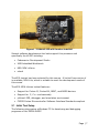
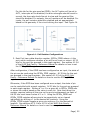
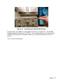
Figure 1 - FRDM-KL25Z with headers installed
Several software development tool sets support this processor and
specifically the KL25Z including:
Codewarrior Development Studio
IAR Embedded Workbench
KEIL MDK uVision
mbed
The KEIL toolset has been selected for this course. A limited free version of
is available, MDK-Lite, which is suitable to meet the development needs of
this course.
The KEIL MDK uVision toolset features:
Support for Cortex-M, Cortex-R4, ARM7, and ARM9 devices
Support for C, C++ and assembly
µVision4 IDE, debugger, and simulation environment
CMSIS Cortex Microcontroller Software Interface Standard compliant
2.1 Initial Tool Setup
The following steps setup a Windows PC for developing and debugging
programs on the FRDM-KL25Z.
Page | 7
Step 1: From the KEIL website (registration required), download and
install KEIL MDK-ARM uVision 5. Note the free MDK-ARM Lite is sufficient
for the lab. (https://www.keil.com/demo/eval/arm.htm)
After installing uVision 5, run "C:\Keil\UV4\PackInstaller.exe" and install
the option for Keil::Kinetis_KLxx_DFP. This will install the appropriate
libraries for the processor used on the board.
Step 2: From the KEIL website, download and install the Freescale
Kinetis OSJTAG Drivers. (http://www.keil.com/download/docs/408.asp)
Step 3: From PE Micro website (registration required), download and
install the OpenSDA Windows USB Drivers.
(http://www.pemicro.com/opensda/)
2.2 Board Setup
The following steps must be executed to allow code to be loaded and
debugged using the KEIL tools and software project used in the labs. This
process only needs to be done once initially on a new board or if there are
problems connecting to the board.
Step 1: From PE Micro website (registration required), download and
extract the OpenSDA Firmware. (http://www.pemicro.com/opensda/)
Step 2: Connect the “USB B” end of a “USB B” to “USB Mini” cable to
the development PC
Step 3: While holding the RST button on the KL25Z, connect the “USB
Mini” connector of the USB cable to the connector labeled SDA on the
KL25Z.
Step 4: Release the RST button. The D4 LED should flash green.
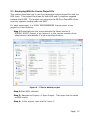
Step 5: In Windows Explorer, open the drive labeled BOOTLOADER.
Page | 8
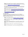
Figure 2 - BOOTLOADER drive
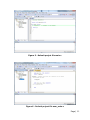
Step 6: From the files extracted in Step 1:, copy the firmware file MSDDEBUG-FRDM-KL25Z_Pemicro_v114.SDA to the BOOTLOADER drive.
Step 7:
Disconnect and reconnect the USB cable from the KL25Z.
Step 8: In Windows Explorer, the drive should now be labeled FRDMKL25Z. Proper installation can be verified by opening the file
SDA_INFO.HTM in the FRDM-KL25Z and verifying the application version
matches that of the firmware file listed in Step 6:.
Figure 3 - FRDM-KL25Z drive
Page | 9
2.3 Developing With the Course Project File
This section describes how to use the customized course project file with the
KEIL tools. This project file allows for both ASM and C programs targeted
towards the KL25Z. The project only supports the PE Micro OpenSDA driver
and only supports loading code into RAM.
For each experiment, it is HIGLY RECOMMENDED that you start a new
project in a new directory.
Step 1: Download from the course website the latest version of
ECE395_ML25Z_Project_#.zip (where # is the version number of the
latest version) and extract it to your working directory.
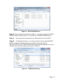
Figure 4 - Files in default project
Step 2: Start KEIL uVision4.
Step 3: Navigate to Project >> Open Project. Then open the file called
ece395.uvproj.
Step 4: In the project, open the file “main.c”.
Page | 10
Figure 5 - Default project file main.c
Figure 6 - Default project file asm_main.s
Page | 11
Step 5: If this is a program in assembly, in “main.c”, uncomment the
beginning of the line asm_main(); and open the file “asm_main.s”.
Step 6: Add your code to the appropriate file, main.c for a C project or
“asm_main.s” for an assembly project. Follow the comments in the
templates to keep the code in the correct sections.
Step 7: Navigate to Project >> Build Target (hotkey F7). In the build
output window, make sure there are no errors and that any warnings
are understood.
Step 8: Ensure the SDA connector on a FRDM-KL25Z running the PE
Micro Firmware (see section 2.2 - Board Setup) is plugged into a USB
cable connected to the PC.
Step 9: Navigate to Debug >> Start/Stop Debug Session (hotkey Ctrl +
F5). (Note a warning about a 32k size limit may appear if you are using
the lite version of the tool, this is ok).
Step 10: At this point, code can be ran, single stepped, etc.
To edit the code, the debug session needs to be stopped, navigate to
Debug >> Start/Stop Debug Session (hotkey Ctrl + F5) and Step 6:
through Step 9: need to be repeated
Page | 12
3 Experiments
3.1 Lab 1 – Microprocessor Operation
Lab Objectives
To learn to create a uVision project then write, assemble and debug
code
To observe and document operation of microprocessor core as it
executes code
Procedure
From the course website, download and print the lab worksheet form for Lab
1.
Follow the steps outlined in section 2.3 which explain how to create a new
project file. Configure the project to be an assembly project by
uncommenting the call to asm_main() in main.c
Add the code for each part to the asm_main.s file.
Build then debug the code as explained in section 2.3. Figure 7 shows the
typical debug window display.
Figure 7, Section A lists the program code.
Figure 7, Section B lists the disassembly of the code. For and assembly
program, this window should match fairly closely the program code. For a C
program, both the C code and generated assembly code will be shown. Also
shown in this window is the address and machine code for each.
Figure 7, Section C shows the registers as the program is debugged.
Figure 7, Section D show the contents of the processor memory. This
window can be displayed with the menu View >> Memory >> Memory 1-4.
The address field sets the address of the memory that is to be displayed.
Step though the code a single line at a time using the “step into” button
.
Observe the behavior of each instruction and log the results on the lab
worksheet.
Page | 13
Figure 7 – Debug window
Page | 14
Part 1: This step demonstrates the basics of memory access and moving
data within the processor.
Add the code shown in Figure 8 to the asm_main.s file.
equate_val
EQU
0x8BADF00D
AREA asm_area, CODE, READONLY
EXPORT asm_main
asm_main ; assembly entry point for C function, do not delete
; Add program code here
LDR
LDR
LDR
LDRH
LDRB
R0,=const_val
R1,const_val
R1,[R0]
R1,[R0]
R1,[R0]
;load address to R0
;load word (32-bit) from memory
LDR
R0,=equate_val
;load value to R0
LDR
STR
R1,=const_val
R0,[R1]
;load address to R1
;load value in R0 to memory at R1
MOV
MOVS
R2,R0
R2,#0
;copy R0 to R2
;clear R2
B
asm_main
;load half word (16-bit) from mem
;load byte (8-bit) from memory
; Put constants here
const_val DCD
0xDEADBEEF
AREA data_area, DATA, READWRITE
; Put variables here
END
Figure 8 – Code for Lab 1 Part 1
Page | 15
Part 2: This step demonstrates some of the basic arithmetic and logic
operations. It is worth noticing that instructions ending with an ‘S’ modify
the application program status register (APSR).
Modify the code as show in Figure 9.
value1
value2
value3
EQU 50
EQU 123
EQU 0xFFFFFFF0
AREA asm_area, CODE, READONLY
EXPORT asm_main
asm_main ; assembly entry point for C function, do not delete
; Add program code here
MOVS R0,#0
;clear R0
LDR R1,=value1
;put value1 in R1
LDR R2,=value2
;put value2 in R2
LDR R3,=value3
;put value3 in R3
MSR
ADDS
SUBS
ADDS
SUBS
APSR,R0
R2,R1
R2,R1
R3,R1
R3,R1
;clear flags
;Add values, update APSR
;Subtract values, update APSR
;Add values, update APSR
;Subtract values, update APSR
MSR
ADD
APSR,R0
R3,R1
;clear flags
;Add values
CMP
CMP
CMP
CMP
CMP
CMP
CMN
R1,R2
R2,R1
R1,R1
R1,#0x40
R2,#0x40
R1,R3
R1,R3
;compare
;compare
;compare
;compare
;compare
;compare
;compare
B
asm_main
immediate
immediate
negative
negative
; Put constants here
AREA data_area, DATA, READWRITE
; Put variables here
END
Figure 9 – Code for Lab 1 Part 2
Page | 16
Part 3: This step demonstrates program flow control operations using
unconditional braches.
Modify the code as show in Figure 10.
AREA asm_area, CODE, READONLY
EXPORT asm_main
asm_main ; assembly entry point for C function, do not delete
; Add program code here
spot1
B
spot3
spot2
B
spot4
spot3
B
spot2
spot4
B
spot1
; Put constants here
AREA data_area, DATA, READWRITE
; Put variables here
END
Figure 10 - Code for Lab 1 Part 3
Page | 17
Part 4:
This step demonstrates the use of conditional branches.
Modify the code as show in Figure 11.
AREA asm_area, CODE, READONLY
EXPORT asm_main
asm_main ; assembly entry point for C function, do not delete
; Add program code here
rst_cnt
MOVS R0,#3
dec_cnt
SUBS R0,#1
BNE
dec_cnt
B
rst_cnt
; Put constants here
AREA data_area, DATA, READWRITE
; Put variables here
END
Figure 11 - Code for Lab 1 Part 4
Page | 18
Part 5: This step demonstrates using linked branches for calling
subroutines.
Modify the code as show in Figure 12.
AREA asm_area, CODE, READONLY
EXPORT asm_main
asm_main ; assembly entry point for C function, do not delete
; Add program code here
loop
LDR R0,=value1
BL
change_value
;call change_val for value1
LDR R0,=value2
BL
change_value
;call change_val for value2
B
;do it again
loop
;change_val takes 32-bit value from memory pointed to by R0
;and modifies it by incrementing, then XORing with the
;address, then clearing all byte the lower byte. This is then
;returned back to the address location in memory
change_value
PUSH {R1,R2}
LDR R1,[R0]
ADD R1,#1
EORS R1,R0
MOVS R2,#0xFF
ANDS R1,R2
STR R1,[R0]
POP {R1,R2}
BX
LR
;Save R1 and R2 to stack
;Get value from memory
;Increment
;XOR with address
;Set mask
;Mask
;Save value back to memory
;Restore R1 and R2
;Return
; Put constants here
AREA data_area, DATA, READWRITE
; Put variables here
value1
SPACE
4
value2
SPACE
4
END
Figure 12 - Code for Lab 1 Part 5
Page | 19
3.2 Lab 2 – General Purpose Inputs and Outputs
Lab Objectives
To learn how to configure the MCU internal peripherals
To learn how to setup and operate the GPIO pins of the MCU
Background
When creating a design using a processor, it is common to need inputs or
outputs that operate in a binary (on/off) fashion. These signals are used for
monitoring user inputs (switches or pushbuttons), driving indicators (lights
or audible), controlling actuators, monitoring/driving discrete control lines
from/to other circuits in the design, or for a variety of other purposes.
Microcontrollers typical will have pins that can be configured as either
outputs that can be driven by or inputs that can be monitored by the
processor. These signals are commonly refer to as general purpose inputs
and outputs (GPIO’s).
The FRDM-KL25Z board provides 53 pins which can be used for assigned
peripheral special functions (e.g. UART IO, DAC outputs, ADC inputs, etc.).
If a specific peripheral which is tied to a given pin is not used in a design,
the pin is available for use as a GPIO. When selecting pins to use as a GPIO,
it is important to avoid pins that are assigned to a special function that will
also be used in the design. For example, if the DAC was to be used in a
design, pins associated with the DAC functions could not be used as GPIO.
For the KL25Z128VLK4 processor used on the KL25Z, section 10.3.1 of the
KL25 Sub-Family - Reference Manual lists a table showing how pins are
mapped to functions. The table lists up to 8 “ALT” options for any given pin.
It can be seen that certain pins can have multiple functions mapped to it. If
the function is set to ALT1, it is configured to be a GPIO.
Pins are grouped into 5 “ports” labeled A though E. The architecture allows
for ports to have up to 32-bits but some ports have less than 32-bits due to
limitations on the number of pins available in the device package. Pins are
numbered 0 to 31. Figure 13 shows how the port pins are mapped to the
headers on the FRDM-KL52Z. For example PTA1 is Port A, Pin 1.
Page | 20
Figure 13 - Header Pin Assignments
(from the FRDM-KL25Z User Manual)
Once a GPIO is selected, several registers must be properly configured in the
processor to allow it to be used as an input or output.
1. Each Port has a separate clock gate that must be enabled if IO
associated with the Port will be used. The SIM_SCGC5 register
contains the controls for the Port clock gates. See section 12.2.9 of
the KL25 Sub-Family - Reference Manual for details on how to enable
the clock gates using the SIM_SCG5 register.
2. Each pin has a pin control register, PORTx_PCRn where x is the the
Port and n is the Pin, that is used to configure the pin behavior. There
are setting fields for the ALT option, interrupt operation, drive strength,
slew rate and pull-up/down resistor configuration. See section 11.5.1
of the KL25 Sub-Family - Reference Manual for details on how to set
the PORTx_PCRn registers.
Page | 21
For this lab for the pins used as GPIO’s, the ALT option will be set to
ALT1, interrupts will be disabled, the drive strengths should be set to
normal, the slew rate should be set to slow and the passive filter
should be disabled. For outputs, the pull resistors will be disabled. For
inputs, the pull resistors should be enabled and set appropriately
based on the geometry if the circuit driving the input. See Figure 14.
Figure 14 - Pull Resistor Configurations
3. Each Port has a data direction register, GPIOx_PDDR where x it the
port, which configures whether a pin will be an input or output. All 32
bits for the port are grouped in the single register. See section 41.2.6
of the KL25 Sub-Family - Reference Manual for details on how to set
the GPIOx_PDDR register.
After configuration, if the GPIO has been configured as an input, the state of
the pin can be read using the GPIOx_PDIR register. All 32 bits for the port
are grouped in the single register. See section 41.2.5 of the KL25 SubFamily - Reference Manual for details on how to use the GPIOx_PDIR
registers.
Otherwise, if the GPIO has been configured as an output, the state of pin
can be controlled with several registers. All 32 bits for the port are grouped
in each single register. Writing a 1 or 0 to a given bit in GPIOx_PDOR sets
or clears the output based on the value in each bit. Note that using this
register requires setting all the pins on the port simultaneously as each of
the 32 bits must have a value of 1 or 0. Using the GPIOx_PSOR and
GPIOx_PCOR registers allows pins to be respectively set or cleared
individually by writing a 1 to the desired bit locations. Using the
GPIOx_PTOR register toggles a given pin writing a 1 to the desired bit
location. See sections 41.2.1 thru 41.2.4 of the KL25 Sub-Family Reference Manual for details on how to use these registers.
Page | 22
There is an LED on the FRDM-KL25Z is a tri-color red/green/blue device.
The common anode is tied to VDD. The three cathodes are tied through
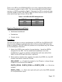
resistors to GPIO’s as listed in Table 1. Because the LED is wired with the
common anode to VDD, the GPIO’s must be driven low to run on the LED
color and driven high to turn off the LED.
Table 1- KL25Z LED GPIO Assignments
LED Color
RED
GREEN
BLUE
GPIO
PTB18
PTB19
PTD1
Required Equipment and Parts
Solderless breadboard
Pushbutton
Jumper wires
Procedure
The aim of this lab is to wire a pushbutton to a GPIO on the FRDM-KL25Z,
then to write software to change the color of the on-board LED when the
button is pushed. The LED colors for pressed vs not pressed may be chosen
at the developers’ discretion.
1. Select the GPIO to be used for the pushbutton. Avoid the GPIO’s
assigned to the LED. On the solderless breadboard, wire the
pushbutton in a pull-up resistor configuration with one side of the
switch to the GPIO and the other to ground.
2. Write code to initialize the registers to enable the GPIO’s for the LED
outputs and switch inputs as follows:
SIM_SCGC5 <<< Enable the clocks for the IO ports, to keep things
simple all the clock can be enabled
PORTB_PCR18, PORTB_PCR19 and PORTD_PCR1 <<< Set to be
outputs
PORTx_PCRn <<< Set to be input with pull-up for the GPIO selected
for the pushbutton input
Page | 23
GPIOB_PDDR[bits 18 and 19] and GPIOD_PDDR[bit 1] <<< Set
to make pins be outputs
GPIOx_PDDR[bits n] <<< Set to make pin input for GPIO selected
for pushbutton
Figure 16 shows some example code on a way to initialize registers.
There is sub-routine called init_gpio that is called from the asm_main
routine. In the example, two registers are initialized using slightly
different methods.
For both registers, there is an equate at the top of the file to assigned
an address to a label matching the name of the register. Note that the
equate can contain math directives to produce the proper value as
shown in the assignment for PORTB_PCR18. This was done to match
the address + offset description used in the processor reference
manual.
In the first method for loading the value to SIM_SCGC5, the code
reads the original value of the register, then OR’s the bits that need to
be set with the original value, then writes the new value back to the
register. This is done to maintain any settings that were previously
set. Note that the value that is being written will turn on all the Port
clocks. This is not ideal for a design with an objective to minimize
power consumption but it is fine for our needs.
The second method used for loading the value into PORTB_PCR18,
directly writes the new value into the register. This is ok here because
the whole register only impacts the behavior of the concerned pin.
Follow these methods to set the remaining registers.
3. Add code in the asm_main loop to:
Read status of push-button
o Use the GPIOx_PDIR register for the input port to read the
inputs
o The appropriate bit can be masked then compared to test if it
is pressed
If pressed, set LED to color 1, clear color 2
o Use the GPIOx_PSOR register to set the appropriate pin to
turn off the one LED color
Page | 24
o Use the GPIOx_PCOR register to clear the appropriate pin to
turn on the other LED color
Else, set LED to color 2, clear color 1
o Do the opposite of the previous step
4. To test the program, build the code and start a debug session. The
system registers can be viewed by selecting Peripherals >> System
Viewer >>> {Register Group}. For this lab, register groups SIM,
PORTB, PORTD, GPIOB and GPIOD should be selected. The values of
the registers should be observed as the program executes ash show in
Figure 15.
Figure 15 - Observing Registers with System Viewer
5. After fully testing the program, demonstrate it to the course instructor
for credit.
Page | 25
SIM_SCGC5
PORTB_PCR18
EQU
EQU
0x40048038
;SIM_SCGC5 address
0x4004A000 + 4 * 18 ;PORTB_PCR18 address
AREA asm_area, CODE, READONLY
EXPORT asm_main
asm_main ;assembly entry point for C function, do not delete
; Add program code here
BL
init_gpio
loop
B loop
init_gpio
LDR R0,=SIM_SCGC5
LDR R1,[R0]
LDR R2,=0x00003E00
ORRS R1,R2
STR R1,[R0]
;Load address of SIM_SCGC5 to R0
;Put value of SIM_SCGC5 into R1
;Load value to turn on all port
;clocks into R2
;OR R2 into R1
;Put value back into SIM_SCGC5
LDR R0,=PORTB_PCR18
LDR R1,=0x00000100
STR R1,[R0]
;Load address of PORTB_PCR18 to R0
;Load value to R1
;Put value into PORTB_PCR18
;add other registers here
;....
BX LR
; Put constants here
AREA data_area, DATA, READWRITE
; Put variables here
END
Figure 16 - Example Code to Initialize Registers
Page | 26
3.3 Lab 3 – Annunciator (GPIO Application)
Lab Objectives
To apply knowledge on the use of GPIO’s gained in lab 2 to solve a
design problem
Problem
A maple syrup factory in Vermont has a problem. They have a holding tank
that stores their product that overflows from time-to-time. When this
happens, an operator in a remote monitoring room is sent to clean up the
mess. They have asked you group to implement an “Annunciator” system
to monitor the holding tank and report its status to the operator in the
monitoring room. The system has two objectives, to notify the operator
when the tank is near full (so they can manually turn off the fill valve), then
to notify the operator when the tank has over flown (so they can be sent to
clean it up).
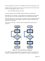
Tank
OLA
Annunciator
FLA
TST
ACK
Syrup
Figure 17 - Annunciator System
There are 4 input to the system. There are two level switches in the tank,
full level alarm (FLA) and overflow level alarm (OLA). On the Annunciator
box in the control room, there are two momentary push buttons,
acknowledge (ACK) and test (TST).
On the Annunciator box, there are 3 outputs from the system, a green ok
indicator, a yellow full indicator and a red overflow indicator.
The system has 6 states as shown in Figure 18.
Page | 27
GRN
FL YEL
FL RED
TST
A
FLA
GRN
B
TST*FLA
FL YEL
ACK*FLA*OLA
C
YEL
D
FLA*OLA
FLA*OLA
OLA
E
OLA
OLA
ACK
FL RED
F
RED
Figure 18 - Annunciator State Diagram
Required Equipment and Parts
Solderless breadboard
2 Pushbuttons
1 DIP switch
1 Red LED
1 Yellow LED
1 Green LED
3 220 ohm resistors
Jumper wires
Procedure
Use the knowledge gained in lab 2 to configure the GPIO’s to monitor the
four inputs and control the three outputs. Write software to implement the
state machine for the annunciator system.
1. Select the GPIO’s to be used for the inputs. Avoid the GPIO’s assigned
to the on-board LED. On the solderless breadboard, wire the 2
pushbuttons and 2 of the DIP stitches to the 4 GPIO’s selected as the
Page | 28
inputs in a pull-up resistor configuration with one side of the switch to
the GPIO and the other side to ground.
2. Select the GPIO’s to be used as the outputs. Avoid the GPIO’s
assigned to the on-board LED. On the solderless breadboard, wire the
3 outputs to the anode’s of the red yellow and green LED’s. Tie the
cathodes of the LED to ground though 200 ohm resistors.
3. Modify the gpio_init routine from lab 2 to setup the GPIO inputs and
outputs appropriately.
4. Add code to handle the states of the Annunciator state machine.
5. Test and debug the code.
6. After fully testing the program, demonstrate it to the course instructor
for credit.
3.4 Lab 4 – UART Serial Port
Lab Objectives
To learn how to setup and operate the MCU serial ports
To create portable functions for serial port initialization and write and
read operations
To learn how to use an oscilloscope to observe a serial waveform
One lab report is required from group
Background
Serial communications is a fundamental principal for microprocessor systems.
In serial communications, data is transferred sequentially bit-by-bit along a
channel in contrast to parallel communications where multiple bits are sent
simultaneously over multiple channels. In modern digital systems, there are
various protocols which employ serial transmission techniques that are
aimed at a variety of applications. Some common examples are: USB
(Universal Serial Bus) which is commonly used to interface peripherals to
computers; SATA (Serial ATA), which is used to interface storage devices in
computers; and Ethernet, which is used for computer networks. Other
examples of serial buses are I2C and SPI (Serial Peripheral Interface) buses
which are commonly found in embedded processor systems as interfaces
busses for memories, DAC’s and ADC, etc and CAN Bus (Controller Area
Network) which is used to interface various systems in vehicles.
Page | 29
One of the simplest implementations of serial communications is the
asynchronous serial port. Historically these were common on personal
computers for uses such as interfacing to external modems, peripherals such
as mice and computer terminals. On PC’s, these serial ports used RS-232
complaint signaling and DB-25 or DE-9 connectors. RS-232 specifies the
electrical characteristics of the signals. In the last decade, serial ports on
PC’s have become rarer features as USB has replaced most of the consumer
applications that were previously handled by serial ports.
In embedded systems and industrial controls, asynchronous serial
communications is still very common and useful. In one common embedded
application, asynchronous serial ports are used for debug console interfaces.
Most microcontrollers feature UART (Universal Asynchronous Receiver
Transmitters) peripherals internal to the microcontroller. A common
implementation would be to connect the microcontroller UART to an RS-232
converter IC (integrated circuit) on the embedded system which would then
interface to the RS-232 serial port on a PC.
In newer PC’s which do not have built in RS-232 serial ports, a USB-to-RS232 converter would be used. These converters usually have a DE-9
connector, RS-232 converter IC and a serial-to-USB converter IC with a USB
cable to interface to the PC. These serial-to-USB converter IC’s are available
from a variety of manufactures (Prolific and FTDI are very common). The
use of these IC’s required a driver to be installed on the PC but typically do
not required any custom firmware to use the IC.
In newer embedded systems (in the Arduino for instance), the RS-232
interface is completely removed and the serial-to-USB IC is directly put on
the embedded board. This allows the embedded system to directly connect
to a PC without the use of a USB-to-RS-232 converter.
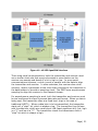
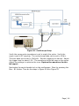
The KL25Z uses a similar approach but uses a secondary ARM processor as
the serial-to-USB interface instead of the serial-to-USB IC. This secondary
ARM processor also serves as the programming and debug interface that is
used to load and test code on the main ARM processor. The functions
performed by the secondary ARM processor are called OpenSDA.
Page | 30
Figure 19 - KL25Z OpenSDA Interface
Then using serial communications, both the transmitter and receiver must
use a similar clock rate that are synchronized in some fashion so the
receiver can sample and decide if a bit is high or low. In some serial
communications schemes, a clock is sent in parallel with the data to align
the transmitter and receiver. In other schemes, the receiver does clock
recovery, where it generates a local clock that is aligned to the transitions in
the data pattern to provide a sampling clock. The UART uses asynchronous
sampling to align the receiver to the transmit stream.
For asynchronous sampling to work, both the transmitter and receiver must
be pre-configured to share the same data rate and format. When no data is
being sent, the transmitter idles at a fixed level, high in the case of
traditional UART’s . When a data byte is to be transmitted, the transmitter
starts will a “start” bit, which is always a low. The transmitter then follows
with the data bits, which are usually sent LSB (least significant bit) first, high
is a “1” and low is a “0”. The transmitter closes the transmission with a
“stop” bit which is always a high.
Page | 31
When the receiver sees the transition from high (idle) to low (start bit), it
knows a data byte is coming. It starts sampling the subsequent bits roughly
1.5 bit periods after the beginning of the start bit. It samples at the bit
period for the number of data bits it has been configured for. The presence
of the stop bit forces the line to go high so the receiver can observe the next
high to low transition. Because the receiver re-synchronizes its sampling
after each transmitted byte, differences of up to about +/-5% are possible in
the transmit and receive clocks.
Idle
Start
Bit 0
(LSB)
Bit 1
Bit 2
High
Bit 3 Bit 4
Bit 5
Bit 6
Bit 7 Stop
(MSB)
Idle
or
next byte
Low
Figure 20 - Asynchronous Serial Transmission
The processor on the KL25Z has 3 UART’s. UART0 is wired on KL25Z to the
Open SDA interface hence it will be used in this lab. The OpenSDA serial
connection is wired to pins PTA1 (RX) and PTA2 (TX). To use a UART0,
several parts of the processor must configured. Code is provided that does
the following.
1. The UART0 clock source select bits (UART0SRC) must be set in the
SIM_SOPT2 register. In the code provided, these bits are set to 01b =
MCGFLLCLK clock or MCGPLLCLK/2 clock. This means either the
MCGFLLCLK (96MHz on the KL25Z) or MCGPLLCLK/2 (48MHz) will be
the clock that drives UART0. The next setting selects which one is
used.
2. The PLL/FLL clock select (PLLFLLSEL) must be set in the SIM_SOPT2
register. In the code provided, this bit is set to 1b = MCGPLLCLK clock
with fixed divide by two. This means the UART0 clock will be 48MHz.
3. The UART0 Clock Gate Control (UART0) in the SIM_SCGC4 register
must be enabled (set to 1).
4. The Port A Clock Gate Control (PORTA) in the SIM_SCGC5 must be
enabled (set to 1). This is because the UART0 will use IO on port A.
5. The Pin Mux Control (MUX) bits of PORTA_PCR1 and PORTA_PCR2
must be set to 010b = Alternative 2. Alternate 2 on these pins is
UART0_RXfor PTA1 and UART0_TX for PTA2.
Page | 32
6. The Over Sampling Ratio (OSR) size must be set in UART0_C4. In the
code provided, it has been set to x8. This factors into the baud rate
calculations.
7. The Baud Rate Modulo Divisor (SBR) must be set in the UART0_BDH
and UART0_BDL registers based on the desired baud rate and the
clock settings. The SBR is a 13 bit long field split between
UART0_BDH and UART0_BDL. The lower 8 bits (SBR[7:0]) are in
UART0_BDL and the upper 5 bits (SBR[12:9]) are the lowest bits in
UART0_BDH.
SBR = clock_rate/(OSR * baud_rate)
clock_rate = 48MHz (based on the settings for UART0SRC and
PLLFLLSEL)
OSR = 8
For baud_rate = 9600 bps
SBR = 48000000/(8 * 9600) = 625 = 0x271
UART0_BDH = 0x02
UART0_BDL = 0x71
8. The Transmitter Enable (TE) and receiver Enable (RE) bits in
UART0_C2 must be set to 1 to enable the transmitter and receiver.
After the UART is configured, the UART can transmit and receive.
Data can be transmitted by writing to the UART Data Register (UART0_D).
Data should only be written to the UART if the transmitter is not busy (e.g.
still sending a byte). The status of the transmitter can be monitored with
the Transmit Data Register Empty Flag (TDRE) in UART Status Register 1
(UART0_S1). When TDRE is 1, the transmitter can be written to.
Received data can be read from the UART Data Register (UART0_D). Data is
available when the Receive Data Register Full Flag (RDRF) in UART0_S1 is 1.
Data should only be read from UART0_D after verifying RDRF is 1.
Data transmitted and received on serial ports is often formatted as ASCII
(American Standard Code for Information Interchange) characters. ASCII
provides a standard way to translate hex bytes to characters (letters, digits,
punctuation, etc). When using a terminal emulator to send text, the data is
usually ASCII.
Page | 33
Figure 21 shows a summary of the registers for UART0. Note that the fields
that are described are in bold. Also note all fields are 8 bits and length and
should be accessed with 8 bit instructions (LDRB and STRB).
Register
Bit 7
Bit 6
Bit 5
Bit 4
Bit 3
Bit 2
Bit 1
Bit 0
UART0_C1
LOOPS
DOZEEN
RSRC
M
WAKE
ILT
PE
PT
UART0_C2
TIE
TCIE
RIE
ILIE
TE
RE
RWU
SBK
UART0_C3
R8T9
R9T8
TXDIR
TXINV
ORIE
NEIE
FEIE
PEIE
UART0_C4
MAEN1
MAEN2
M10
UART0_C5
TDMAE
0
RDMAE
0
0
0
BOTHEDGE
RESYNCDIS
UART0_S1
TDRE
TC
RDRF
IDLE
OR
NF
FE
PF
UART0_S2
LBKDIF
RXEDGIF
MSBF
RXINV
RWUID
BRK13
LBKDE
RAF
UART0_BDH
LBKDIE
RXEDGIE
SBNS
OSR
SBR[12:8]
UART0_BDL
SBR[7:0]
UART0_D
Data[7:0]
Figure 21 - UART0 Registers
(see section 39 of KL25 Sub-Family Reference Manual for details)
Required Equipment and Parts
Tektronix DPO2012B Oscilloscope (in lab)
Oscilloscope Probe (from stockroom)
Tektronix DPO2COMP Computer Serial Module (from stockroom)
Jumper wires
Procedure
3.4.1 Lab 4, Part 1: Reading and writing characters for the UART
The objective of this part is to develop a program to initialize the UART and
enter a loop that reads a character from the UART and then writes it back to
the UART. This is known as “echoing” back. A terminal emulator running on
Page | 34
the PC will be used to send characters to the board and display what the
board sends back.
A starting point for the code for this program is given in Figure 22. This
code needs to have the char_out and char_in functions completed.
Page | 35
SIM_SOPT2
SIM_SCGC4
SIM_SCGC5
EQU
EQU
EQU
0x40048004
0x40048034
0x40048038
PORTA_PCR1
PORTA_PCR2
EQU
EQU
0x40049000 + 4 * 1
0x40049000 + 4 * 2
PORTE_PCR20
PORTE_PCR21
EQU
EQU
0x4004D000 + 4 * 20
0x4004D000 + 4 * 21
UART0_BDH
UART0_BDL
UART0_C1
UART0_C2
UART0_S1
UART0_S2
UART0_C3
UART0_D
UART0_MA1
UART0_MA2
UART0_C4
UART0_C5
EQU
EQU
EQU
EQU
EQU
EQU
EQU
EQU
EQU
EQU
EQU
EQU
0x4006A000
0x4006A001
0x4006A002
0x4006A003
0x4006A004
0x4006A005
0x4006A006
0x4006A007
0x4006A008
0x4006A009
0x4006A00A
0x4006A00B
AREA
EXPORT
EXPORT
EXPORT
EXPORT
asm_area, CODE, READONLY
asm_main
UART0Init
char_in
char_out
asm_main ;assembly entry point for C function, do not delete
; Add program code here
BL
UART0Init
BL
BL
b
char_in
char_out
loop
loop
; read char from UART, char in R0
; send char in R0 to UART
; When char_out is called, R0 contains
; the char to be sent out the UART
char_out FUNCTION
BX LR
ENDFUNC
Page | 36
; When char_in returns, R0 contains
; the char that was received
char_in FUNCTION
BX LR
ENDFUNC
UART0Init FUNCTION
; SIM_SOPT2[UART0SRC] = 01b (MCGFLLCLK or MCGPLLCLK/2 clock)
; and SIM_SOPT2[PLLFLLSEL] = 1b for MGCPLLCLK/2
LDR R0,=SIM_SOPT2 ;Load address of SIM_SOPT2 to R0
LDR R1,[R0]
;Put present value of SIM_SOPT2 into R1
LDR R2,=0xF3FEFFFF ;Load bits to clear
ANDS R1,R2
;AND values to clear bits
LDR R2,=0x04010000 ;Load bits to set
ORRS R1,R2
;OR values to set bits
STR R1,[R0]
;Put value back into SIM_SOPT2
; SIM_SCGC4[UART0] = 1
LDR R0,=SIM_SCGC4
LDR R1,[R0]
LDR R2,=0x00000400
ORRS R1,R2
STR R1,[R0]
; SIM_SCGC5[PORTE thru A] = 1, turn on clock for all ports
LDR R0,=SIM_SCGC5
;Load address of SIM_SCGC5 to R0
LDR R1,[R0]
;Put value of SIM_SCGC5 into R1
LDR R2,=0x00003E00 ;Load value to turn on all port
;clocks into R2
ORRS R1,R2
;OR R2 into R1
STR R1,[R0]
;Put value back into SIM_SCGC5
; PORTA_PCR1 , Clear ISF and set MUX = 2
LDR R0,=PORTA_PCR1
LDR R1,[R0]
LDR R2,=0x01000200
ORRS R1,R2
STR R1,[R0]
; PORTA_PCR2 , Clear ISF and set MUX = 2
LDR R0,=PORTA_PCR2
LDR R1,[R0]
LDR R2,=0x01000200
ORRS R1,R2
STR R1,[R0]
Page | 37
; UART0_C4[OSR]= 0x07 (for osr = x8)
LDR R0,=UART0_C4
MOVS R1,#0x07
STRB R1,[R0]
;
;
;
;
;
9600 baud
uart0_baud_clk = MGCPLLCLK/2 = 96MHz/2 = 48MHz
SBR = uart0_baud_clk/(baud*osr)
SBR = 48MHz/(9600 * 8)
SBR = 625 = (0x0271)
; UART0_BDH = 0x02
LDR R0,=UART0_BDH
MOVS R1,#0x02
STRB R1,[R0]
; UART0_BDL = 0x71
LDR R0,=UART0_BDL
MOVS R1,#0x71
STRB R1,[R0]
; UART0_C2 = 0x02 (TE and RE = 1)
LDR R0,=UART0_C2
MOVS R1,#0x0C
STRB R1,[R0]
BX LR
ENDFUNC
; Put constants here
AREA data_area, DATA, READWRITE
; Put variables here
END
Figure 22 - Starting Code to Serial Programs
The aim is for the char_out, char_in and UART0Init functions to be callable
from the main C program for use in subsequent experiments. The EXPORT
and FUCNCTION, and ENDFUN statements make these runtimes appear as
functions in C.
When C calls a function, the first four parameters are passed to the function
in R0, R1, R2 and R3. So if the template for char_out in C is:
extern void char_out(unsigned char);
Page | 38
Then the character to be sent out the UART will be the first parameter in R0.
Likewise, when a function return a value, the value that will be returned is in
R0. So if the template for char_in in C is:
extern unsigned char char_in(void);
Then the character that the UART received should be returned in R0.
Note that char_in and char_out are defined as “unsigned char”, this means
that they will be only 8 bits in length which is the length the UART uses.
When writing the char_out and char_in routines, only use registers R0 to R3
and R12 as using any other registers requires the values to be saved and
restored in the function.
The char_out and char_in routines should implement the logic shown in
Figure 23.
No
char_out
(char in R0)
char_in
Read
UART0_S1
Read
UART0_S1
Does
UART0_S1.TDRE = 1
?
Yes
No
Does
UART0_S1.RDRF = 1
?
Yes
Write R0 to
UART0_D
Read UART0_D
To R0
Return
Return
(char in R0)
Figure 23 - char_out and char_in diagrams
The UART0Init subroutine should be completely functional as provided. By
default, it configures UART0 to use 8 data bits, no parity, 1 stop bit and a
Page | 39
baud rate of 9600 bps. The clock source is configured to be MGCPLLCLK/2
which operates at 48MHz.
The asm_main routine is complexly functional as provided. asm_main calls
the UART0Init subroutine then enters a loop that calls char_in followed by
char_out. char_in should wait for the user to enter a character into the
terminal. When a character is entered, char_in should return the character
in R0. char_out is then called which should be echoed back to the user.
This process will then repeat indefinitely.
After completing the char_in and char_out routines connect the KL25Z to the
PC. Build, debug and then run the code onto the board a usual. Open Tera
Term on the PC that is connected to the board (other terminal programs can
be used but Tera Term is recommended).
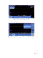
When Tera Term starts, select New Connection, Serial, then the COM port
labeled OpenSDA in the port pull-down. The hit the OK button. (Figure 24)
Figure 24 - Tera Term New Connection
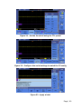
Next select Setup >>> Serial port. In the Serial port setup dialog, set the
baud rate, data, parity, stop and flow control to match the KL25Z settings.
In the default case use: Baud: 9600, Data: 8 bit, Parity: none, Stop: 1 bit
and Flow control: none. Then click the OK button. (Figure 25)
Page | 40
With the code running on the KL25Z and Tera Term setup properly, anything
typed on the Tera Term console will be echoed back and displayed in the
console window. (Figure 26).
Next stop the code running on the KL25Z then type characters in Tera Term.
Lab report: What happens and why?
Next add a second “BL char_out” line to the program after the first but
before the “b loop” statement. Build and run the code. Lab report: What
happens and why?
Figure 25 - Tera Term Serial Port Setup
Page | 41
Figure 26 - Tera Term Displaying Echoed Characters
3.4.2 Lab 4, Part 2: Observing the Serial Port on the Oscilloscope
The objective of this part of the lab is to observe the serial port output on
the oscilloscope. The code will be modified to continuously stream a single
character. Then the oscilloscope will be used to view the output waveform.
Oscilloscope traces will be captured for multiple UART configurations and
analyzed both manually and with the serial decode utility on the scope.
Modify the code from the first part as follows:
In asm_main before the loop but after the call to UART0Init, load R0 with
the ASCII code for the group (bench) number.
In the loop in asm_main, remove the call to char_in and add a call to a delay
routine. The delay is to add some time between sending so it is easy to
observe individual characters on the oscilloscope.
Run the code and verify output of the characters on Tera term.
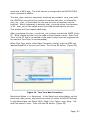
With the oscilloscope off, install the Tektronix Computer Serial Module
(DPO2COMP) into the DPO2012B oscilloscope (Figure 27).
Page | 42
Figure 27 - Installing the DPO2COMP Module
Connect the oscilloscope to the KL25Z as shown in Figure 28. The UART0
transmit signal is output on pin PTA2. Use a scope probe to view the signal.
Connect the ground of the scope probe to one of the ground pins on the
board.
Turn on the oscilloscope.
Page | 43
Figure 28 - Oscilloscope Setup
Verify the scope probe impedance is set to match the probe. Verify the
scope is set to DC coupling. The vertical amplitude can be set to 1V/div.
The time base can be set to 10uS/div. Set the triggering to manual. Adjust
the trigger level to about 1.5V. The waveform should be seen on the scope.
Adjust the settings to optimize the view. Capture the waveform for the
lab report.
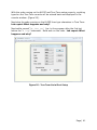
Next setup the serial decode tool on the oscilloscope. Start by pressing the
Bus – B1 button. Then do the steps in Figure 29 thru Figure 35.
Page | 44
Figure 29 - Select bus type , RS-232
Figure 30 - Select the scope channel connected to the TX line
Page | 45
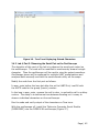
Figure 31 - Set the threshold using the TTL preset
Figure 32 - Configure the serial settings to match the TX config
Figure 33 - Apply a label
Page | 46
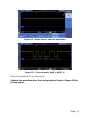
Figure 34 - Select how to view the characters
Figure 35 - The end result, 0x65 = ASCII 'e'
Store the waveform for the lab report.
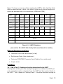
Capture the waveforms for the configurations listed in Figure 36 for
the lab report.
Page | 47
ASCII Character
Baud Rate
Data Bits
Parity
Stop Bits
Group number
9600
8
None
1
Group number
19200
8
None
1
Group number
115200
8
None
1
Last name initial of
report author
115200
8
None
1
Figure 36 - Capture Waveform Settings
3.4.3 Lab 4, Lab report
For the lab report on this lab, be sure to include:
A description of how the lab was performed.
For Part 1, observed results and answers to two highlighted questions
For Part 2, eight waveforms, (manual identification and serial decode of the
four settings listed). On the manual identification of the serial waveforms,
identify:
the voltage levels for high and low
bit time
start bit, data bits 0 thru 7, stop bit
data bit values (0/1)
match the data bits to the ASCII character value
Also include the new code that was written (e.g. char_in and char_out
routines) and any changes made for each of the different setting
configurations.
3.5 Lab 5 – Calculator (UART Application)
Lab Objectives
To apply knowledge on the use of serial ports gained in lab 4 to solve a
design problem
3.6 Lab 6 – Digital-to-Analog Converter
Lab Objectives
Page | 48
To learn how to setup and operate the MCU digital-to-analog converter
(DAC)
To use the DAC to create a waveform generator
3.7 Lab 7 – Analog-to-Digital Converter
Lab Objectives
To learn how to setup and operate the MCU analog-to-digital converter
(ADC)
To use the ADC to create a voltmeter
3.8 Lab 8 – Interrupts and Exceptions
Lab Objectives
To learn how to setup and use interrupts and exceptions in the MCU
Page | 49
4 Troubleshooting
Message: Error #5 Cannot open source input file “MKL25Z4.h”
Cause: Kinetis KL25Z support pack not loaded after installing KEIL uVision
5.
Fix: Follow procedure in section 2.1 to install the Keil::Kinetis_KLxx_DFP
support pack.
Message: Error #A1163E Unknown opcode code XXXX, expected opcode or
macro
Cause: Label not in first character position in line of code.
Fix: Make sure all labels are in the first column.
Message: startup_MKL25Z4.s: error: A1023E: File "startup_MKL25Z4.s"
could not be opened: No such file or directory
Cause: Caused by opening the project directly from the project zip file.
Fix: Extract the zip file, then open the project.
5 Document Change History
Version
Date
By
Changes
3.00
3.01
3.02
1/14/2014
1/20/2014
1/29/2014
DJH
DJH
DJH
3.03
1/31/2014
DJH
3.04
3.05
2/10/2014
3/26/2014
DJH
DJH
Initial release for comment on sections 1, 2 and 3.1.
Completed lab 1 and added course objectives.
Added lab 2 and modified initial install instructions for
uVision 5.
Minor corrections to code in lab 1 and additions to
troubleshooting section.
Added lab 3.
Added lab 4.
Page | 50