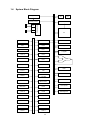
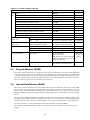
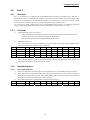
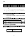
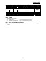
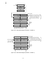
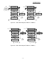
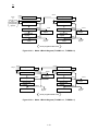
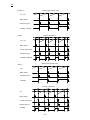
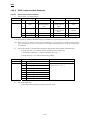
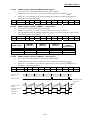
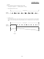
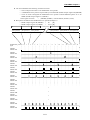
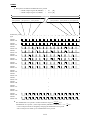
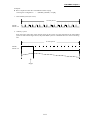
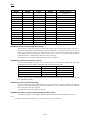
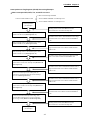
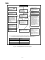
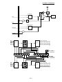
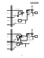
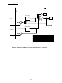
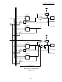
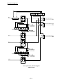
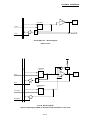
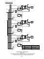
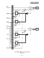
1
CMOS 8-BIT MICROCONTROLLER LC875W00 SERIES USER’S MANUAL http://onsemi.com REV : 1.00 ON Semiconductor Digital Solution Division Microcontroller & Flash Business Unit ON Semiconductor and the ON logo are registered trademarks of Semiconductor Components Industries, LLC (SCILLC). SCILLC owns the rights to a number of patents, trademarks, copyrights, trade secrets, and other intellectual property. A listing of SCILLC’s product/patent coverage may be accessed at www.onsemi.com/site/pdf/Patent-Marking.pdf. SCILLC reserves the right to make changes without further notice to any products herein. SCILLC makes no warranty, representation or guarantee regarding the suitability of its products for any particular purpose, nor does SCILLC assume any liability arising out of the application or use of any product or circuit, and specifically disclaims any and all liability, including without limitation special, consequential or incidental damages. “Typical” parameters which may be provided in SCILLC data sheets and/or specifications can and do vary in different applications and actual performance may vary over time. All operating parameters, including “Typicals” must be validated for each customer application by customer’s technical experts. SCILLC does not convey any license under its patent rights nor the rights of others. SCILLC products are not designed, intended, or authorized for use as components in systems intended for surgical implant into the body, or other applications intended to support or sustain life, or for any other application in which the failure of the SCILLC product could create a situation where personal injury or death may occur. Should Buyer purchase or use SCILLC products for any such unintended or unauthorized application, Buyer shall indemnify and hold SCILLC and its officers, employees, subsidiaries, affiliates, and distributors harmless against all claims, costs, damages, and expenses, and reasonable attorney fees arising out of, directly or indirectly, any claim of personal injury or death associated with such unintended or unauthorized use, even if such claim alleges that SCILLC was negligent regarding the design or manufacture of the part. SCILLC is an Equal Opportunity/Affirmative Action Employer. This literature is subject to all applicable copyright laws and is not for resale in any manner. Contents Chapter 1 Overview ······································································· 1-1 1.1 1.2 1.3 1.4 1.5 1.6 Overview ······················································································ 1-1 Features ······················································································ 1-1 Pinout ·························································································· 1-5 System Block Diagram ···································································· 1-6 Pin Functions ················································································ 1-7 Port Output Types ········································································· 1-10 Chapter 2 Internal Configuration ····················································· 2-1 2.1 2.2 2.3 2.4 2.5 2.6 2.7 2.8 2.9 2.10 2.11 Memory Space ·············································································· 2-1 Program Counter (PC) ···································································· 2-1 Program Memory (ROM) ································································· 2-2 Internal Data Memory (RAM) ···························································· 2-2 Accumulator/A Register (ACC/A) ······················································· 2-3 B Register (B)················································································ 2-3 C Register (C) ··············································································· 2-4 Program Status Word (PSW) ···························································· 2-4 Stack Pointer (SP) ·········································································· 2-5 Indirect Addressing Registers ··························································· 2-5 Addressing Modes·········································································· 2-6 2.11.1 2.11.2 2.11.3 2.11.4 2.11.5 2.11.6 2.11.7 Immediate Addressing (#) ······························································· 2-6 Indirect Register Indirect Addressing ([Rn]) ········································· 2-7 Indirect Register + C Register Indirect Addressing ([Rn,C]) ···················· 2-7 Indirect Register (R0) + Offset Value Indirect Addressing ([off]) ··············· 2-8 Direct Addressing (dst) ··································································· 2-8 ROM Table Look-up Addressing ······················································· 2-9 External Data Memory Addressing ···················································· 2-9 2.12 Wait Sequence ············································································· 2-10 2.12.1 2.12.2 Wait Sequence Occurrence ····························································2-10 What is a Wait Sequence? ·····························································2-10 Chapter 3 Peripheral System Configuration ······································ 3-1 3.1 Port 0 ·························································································· 3-1 3.1.1 3.1.2 3.1.3 3.1.4 3.1.5 3.2 Overview ····················································································· 3-1 Functions····················································································· 3-1 Related Registers ·········································································· 3-2 Options ······················································································· 3-4 HALT and HOLD Mode Operation····················································· 3-4 Port 1 ·························································································· 3-5 3.2.1 Overview ····················································································· 3-5 i Contents 3.2.2 3.2.3 3.2.4 3.2.5 3.3 Port 2 ·························································································· 3-9 3.3.1 3.3.2 3.3.3 3.3.4 3.3.5 3.4 Overview ····················································································3-24 Functions····················································································3-24 Related Registers ·········································································3-24 Options ······················································································3-25 HALT and HOLD Mode Operation····················································3-25 Port B ························································································· 3-26 3.8.1 3.8.2 3.8.3 3.8.4 3.8.5 3.9 Overview ····················································································3-23 Functions····················································································3-23 Related Registers ·········································································3-23 HALT and HOLD Mode Operation····················································3-23 Port A ························································································· 3-24 3.7.1 3.7.2 3.7.3 3.7.4 3.7.5 3.8 Overview ····················································································3-17 Functions····················································································3-17 Related Registers ·········································································3-18 Options ······················································································3-22 HALT and HOLD Mode Operation····················································3-22 Port 8 ························································································· 3-23 3.6.1 3.6.2 3.6.3 3.6.4 3.7 Overview ····················································································3-15 Functions····················································································3-15 Related Registers ·········································································3-15 Options ······················································································3-16 HALT and HOLD Mode Operation····················································3-16 Port 7 ························································································· 3-17 3.5.1 3.5.2 3.5.3 3.5.4 3.5.5 3.6 Overview ····················································································· 3-9 Functions····················································································· 3-9 Related Registers ·········································································3-10 Options ······················································································3-14 HALT and HOLD Mode Operation····················································3-14 Port 3 ························································································· 3-15 3.4.1 3.4.2 3.4.3 3.4.4 3.4.5 3.5 Functions····················································································· 3-5 Related Registers ·········································································· 3-5 Options ······················································································· 3-8 HALT and HOLD Mode Operation····················································· 3-8 Overview ····················································································3-26 Functions····················································································3-26 Related Registers ·········································································3-26 Options ······················································································3-27 HALT and HOLD Mode Operation····················································3-27 Port C ························································································· 3-28 3.9.1 3.9.2 Overview ····················································································3-28 Functions····················································································3-28 ii Contents 3.9.3 3.9.4 3.9.5 Related Registers ·········································································3-28 Options ······················································································3-29 HALT and HOLD Mode Operation····················································3-29 3.10 Port E ························································································· 3-30 3.10.1 3.10.2 3.10.3 3.10.4 Overview ····················································································3-30 Functions····················································································3-30 Related Registers ·········································································3-30 HALT and HOLD Mode Operation····················································3-31 3.11 Port F ························································································· 3-32 3.11.1 3.11.2 3.11.3 3.11.4 Overview ····················································································3-32 Functions····················································································3-32 Related Registers ·········································································3-32 HALT and HOLD Mode Operation····················································3-33 3.12 Timer/Counter 0 (T0) ····································································· 3-34 3.12.1 3.12.2 3.12.3 3.12.4 Overview ····················································································3-34 Functions····················································································3-34 Circuit Configuration ·····································································3-36 Related Registers ·········································································3-41 3.13 High-speed Clock Counter ······························································ 3-44 3.13.1 3.13.2 3.13.3 3.13.4 Overview ····················································································3-44 Functions····················································································3-44 Circuit Coufiguration ·····································································3-45 Related Registers ·········································································3-46 3.14 Timer/Counter 1 (T1) ····································································· 3-48 3.14.1 3.14.2 3.14.3 3.14.4 Overview ····················································································3-48 Functions····················································································3-48 Circuit Configuration ·····································································3-50 Related Registers ·········································································3-55 3.15 Timers 4 and 5 (T4, T5) ·································································· 3-59 3.15.1 3.15.2 3.15.3 3.15.4 Overview ····················································································3-59 Functions····················································································3-59 Circuit Configuration ·····································································3-59 Related Registers ·········································································3-61 3.16 Timers 6 and 7 (T6, T7) ·································································· 3-63 3.16.1 3.16.2 3.16.3 3.16.4 Overview ····················································································3-63 Functions····················································································3-63 Circuit Configuration ·····································································3-63 Related Registers ·········································································3-65 3.17 Base Timer (BT) ··········································································· 3-67 3.17.1 3.17.2 3.17.3 Overview ····················································································3-67 Functions····················································································3-67 Circuit Configuration ·····································································3-68 iii Contents 3.17.4 Related Registers ·········································································3-69 3.18 Serial Interface 0 (SIO0) ································································· 3-71 3.18.1 3.18.2 3.18.3 3.18.4 3.18.5 3.18.6 Overview ····················································································3-71 Functions····················································································3-71 Circuit Configuration ·····································································3-72 Related Registers ·········································································3-75 SIO0 Communication Examples ······················································3-77 SIO0 HALT Mode Operation ···························································3-79 3.19 Serial Interface 1 (SIO1) ································································· 3-80 3.19.1 3.19.2 3.19.3 3.19.4 3.19.5 Overview ····················································································3-80 Functions····················································································3-80 Circuit Configuration ·····································································3-81 SIO1 Communication Examples ······················································3-85 Related Registers ·········································································3-89 3.20 Serial Interface 2 (SIO2) ································································· 3-91 3.20.1 3.20.2 3.20.3 3.20.4 3.20.5 Overview ····················································································3-91 Functions····················································································3-91 Circuit Configuration ·····································································3-91 SIO2 Communication Examples ······················································3-92 Related Registers ·········································································3-93 3.21 Asynchronous Serial Interface 1 (UART1) ·········································· 3-96 3.21.1 3.21.2 3.21.3 3.21.4 3.21.5 3.21.6 Overview ····················································································3-96 Functions····················································································3-96 Circuit Configuration ·····································································3-97 Related Registers ······································································· 3-100 UART1 Continuous Communication Processing Examples ················· 3-104 UART1 HALT Mode Operation ······················································ 3-106 3.22 Asynchronous Serial Interface 2 (UART2) ········································ 3-107 3.22.1 3.22.2 3.22.3 3.22.4 3.22.5 3.22.6 Overview ·················································································· 3-107 Functions·················································································· 3-107 Circuit Configuration ··································································· 3-108 Related Registers ······································································· 3-111 UART2 Continuous Communication Processing Examples ················· 3-115 UART2 HALT Mode Operation ······················································ 3-117 3.23 PWM0 / PWM1 ··········································································· 3-118 3.23.1 3.23.2 3.23.3 3.23.4 Overview ·················································································· 3-118 Functions·················································································· 3-118 Circuit Configuration ··································································· 3-119 Related Registers ······································································· 3-120 3.24 PWM4 / PWM5 ··········································································· 3-126 3.24.1 3.24.2 Overview ·················································································· 3-126 Functions·················································································· 3-126 iv Contents 3.24.3 3.24.4 3.24.5 Circuit Configuration ··································································· 3-127 Related Registers ······································································· 3-128 Setting Up the PWM4 and PWM5 Output Ports ······························· 3-129 3.25 8-bit AD Converter (ADC) ····························································· 3-134 3.25.1 3.25.2 3.25.3 3.25.4 Overview ·················································································· 3-134 Functions·················································································· 3-134 Circuit Configuration ··································································· 3-135 Related Registers ······································································· 3-135 Chapter 4 Control Functions ··························································· 4-1 4.1 Interrupt Function ··········································································· 4-1 4.1.1 4.1.2 4.1.3 4.1.4 4.2 System Clock Generator Function ····················································· 4-6 4.2.1 4.2.2 4.2.3 4.2.4 4.3 Overview ····················································································4-13 Functions····················································································4-13 Related Registers ·········································································4-14 Reset Function ············································································· 4-19 4.4.1 4.4.2 4.4.3 4.5 Overview ····················································································· 4-6 Functions····················································································· 4-6 Circuit Configuration ······································································ 4-7 Related Registers ·········································································· 4-9 Standby Function ·········································································· 4-13 4.3.1 4.3.2 4.3.3 4.4 Overview ····················································································· 4-1 Functions····················································································· 4-1 Circuit Configuration ······································································ 4-2 Related Registers ·········································································· 4-3 Overview ····················································································4-19 Functions····················································································4-19 Reset State ·················································································4-20 Watchdog Timer Function ······························································· 4-21 4.5.1 4.5.2 4.5.3 4.5.4 4.5.5 Overview ····················································································4-21 Functions····················································································4-21 Circuit Configuration ·····································································4-21 Related Registers ·········································································4-22 Using the Watchdog Timer ·····························································4-24 Appendix I Special Function Register (SFR) Map ······························AI (1-9) Appendix II Port Block Diagrams ················································ AII (1-13) v LC875W00 Chapter 1 1. Overview 1.1 Overview The LC875W00 series is an 8-bit microcontroller that, centered around a CPU running at a minimum bus cycle time of 83.3 ns, integrates on a single chip a number of hardware features such as 128K-byte flash ROM (onboard programmable), 4K-byte RAM, a sophisticated 16-bit timer/counter (may be divided into 8-bit timers), a 16-bit timer/counter (may be divided into 8-bit timers or 8-bit PWM modules), four 8-bit timers with a prescaler, a base timer serving as a time-of-day clock, a high-speed clock counter, two synchronous SIO interfaces with automatic transfer function, an asynchronous/synchronous SIO interface, two UART interfaces (full duplex), four 12-bit PWM modules, an 8-bit 15-channel AD converter, a system clock frequency divider, an internal reset circuit, and a 29-source 10-vector interrupt feature. 1.2 ● Features ROM LC875W00 series LC87F5WC8A: 131072 8 bits (flash ROM) Capable of onboard programming with a wide range of supply voltages: 2.7 to 5.5V. Block erasable in 128-byte units ● RAM LC875W00 series LC87F5WC8A: 4096 9 bits ● Minimum bus cycle time 83.3 ns (at 12 MHz) Note: The bus cycle time here refers to the ROM read speed. ● Minimum instruction cycle time (Tcyc) 250 ns (at 12 MHz) ● Ports Normal withstand voltage I/O ports Ports whose input/output can be specified in 1-bit units: 64 (P1n, P2n, P3n, P70 to P73, P8n, PAn, PBn, PCn, S2Pn, PWM0, PWM1, XT2) Ports whose input/output can be specified in 2-bit units: 16 (PEn, PFn) Ports whose input/output can be specified in 4-bit units: 8 (P0n) Normal withstand voltage input ports: Dedicated oscillator ports: Reset pins: Power pins: 1 (XT1) 2 (CF1, CF2) 1 (RES) 8 (VSS1 to VSS4, VDD1 to VDD4) 1-1 ● Timers ● Timer 0: 16-bit timer/counter with capture registers Mode 0: Mode 1: Mode 2: Mode 3: ● 8-bit timer with an 8-bit programmable prescaler (with two 8-bit capture registers) 2 channels 8-bit timer with an 8-bit programmable prescaler (with two 8-bit capture registers) + 8-bit counter (with two 8-bit capture registers) 16-bit timer with an 8-bit programmable prescaler (with two 16-bit capture registers) 16-bit counter (with two 16-bit capture registers) Timer 1: 16-bit timer/counter that supports PWM/toggle output Mode 0: Mode 1: Mode 2: Mode 3: 8-bit timer with an 8-bit prescaler (with toggle output) + 8-bit timer/counter (with toggle output) 8-bit PWM with an 8-bit prescaler 2 channels 16-bit timer/counter with an 8-bit prescaler (with toggle output) (toggle output also possible from the low-order 8 bits) 16-bit timer with an 8-bit prescaler (with toggle output) (The low-order 8 bits can be used as PWM.) ● Timer 4: 8-bit timer with a 6-bit prescaler ● Timer 5: 8-bit timer with a 6-bit prescaler ● Timer 6: 8-bit timer with a 6-bit prescaler (with toggle output) ● Timer 7: 8-bit timer with a 6-bit prescaler (with toggle output) ● Base timer 1) 2) The clock can be selected from among a subclock (32.768 kHz crystal oscillator), system clock, and timer 0 prescaler output. Interrupts are programmable in 5 different time schemes. ● High-speed clock counter 1) Capable of counting clocks with a maximum clock rate of 24 MHz (at a main clock of 12 MHz). 2) Real-time output ● Serial Interface (SIO) ● SIO0: 8-bit synchronous serial interface 1) 2) ● LSB first / MSB first is selectable. Built-in 8-bit baudrate generator (maximum transfer clock rate = ● Tcyc) 3) Automatic continuous data communication (1 to 256 bits) SIO1: 8-bit asynchronous/synchronous serial interface Mode 0: Mode 1: Mode 2: Mode 3: ● 4 3 Synchronous 8-bit serial I/O (2- or 3-wire configuration, 2 to 512 Tcyc transfer clock) Asynchronous serial I/O (half-duplex, 8 data bits, 1 stop bit, 8 to 2048 Tcyc baudrate) Bus mode 1 (start bit, 8 data bits, 2 to 512 Tcyc transfer clock) Bus mode 2 (start detection, 8 data bits, stop detection) SIO2: 8-bit synchronous serial interface 1) 2) LSB first 3) Automatic continuous data communication (1 to 32 bytes) Built-in 8-bit baudrate generator (maximum transfer clock rate = UART: 2 channels 1) Full duplex 2) Data length: 7/8/9 bits selectable 3) Stop bit: 1 bit (2 bits in continuous data transmission) 4) Built-in baudrate generator ( 16 to 8192 Tcyc baudrate) 3 3 1-2 4 3 Tcyc) LC875W00 Chapter 1 ● AD converter: 8 bits 15 channels ● PWM: Variable-period 12-bit PWM 4 channels ● Remote control receiver circuit (multiplexed with P73/ INT3/T0IN pin) Noise filtering function (noise filter time constant selectable from among 1 Tcyc, 32 Tcyc, and 128 Tcyc) Noise filtering function is available for the INT3, T0IN, or T0HCP signals at pin P73. If P73 is read with an instruction, the signal level at the pin is read regardless of the noise filtering function. ● Watchdog timer 1) Watchdog timer with an external RC circuit 2) Interrupt or system reset is selectable. ● Clock output function 1 1 1 1 1 , 1 , or 1 frequency of the source oscillator clock 1) Capable of generating , , , , 1 2 4 8 16 32 64 selected as the system clock. 2) Capable of generating the source oscillator clock for the subclock. ● Interrupts ● 29 sources, 10 vector addresses 1) 2) Provides three levels (low (L), high (H), and highest (X)) of multiplex interrupt control. Any interrupt request of the level equal to or lower than the current interrupt is not accepted. When interrupt requests to two or more vector addresses occur at the same time, the interrupt of the highest level takes precedence over the other interrupts. For interrupts of the same level, the interrupt into the smallest vector address is given priority. No. 1 Vector 00003H Level X or L INT0 Interrupt Source 2 0000BH X or L INT1 3 00013H H or L INT2/T0L/INT4 4 0001BH H or L INT3/INT5/Base timer 0/ Base timer 1 5 00023H H or L T0H/INT6 6 0002BH H or L T1L/T1H/INT7 7 00033H H or L SIO0/UART1 receive/ UART2 receive 8 0003BH H or L SIO1/SIO2/UART1 transmit/ UART2 transmit 9 00043H H or L ADC/T6/T7/PWM4, PWM5 10 0004BH H or L Port 0/T4/T5/ PWM0, PWM1 • Priority levels: X > H > L • When interrupts of the same level occur at the same time, an interrupt with the smallest vector address is given priority. ● Subroutine stack levels: Up to 2048 levels (stack is allocated in RAM) ● High-speed multiplication/division instructions 16 bits 8 bits (5 Tcyc execution time) 24 bits 16 bits (12 Tcyc execution time) 16 bits 8 bits (8 Tcyc execution time) 24 bits 16 bits (12 Tcyc execution time) ● Oscillator circuits RC oscillator circuit (internal): CF oscillator circuit: Crystal oscillator circuit: For system clock For system clock (Rf built in) For low-speed system clock 1-3 ● Internal reset function Power-on reset (POR) function 1) POR resets the system at the time when the power is turned on. ● System clock divider function 1) Capable of running on low current. 2) The minimum instruction cycle time can be selected from among 250 ns, 500 ns, 1.0 µs, 2.0 µs, 4.0 µs, 8.0 µs, 16.0 µs, 32.0 µs, and 64.0 µs (at a main clock rate of 12 MHz). ● Standby function ● HALT mode: Halts instruction execution while allowing the peripheral circuits to continue operation. 1) 2) ● HOLD mode: Suspends instruction execution and operation of the peripheral circuits. 1) 2) ● Oscillation is not halted automatically. Released by system reset or occurrence of an interrupt. The CF, RC, and crystal oscillators automatically stop operation. There are three ways of releasing HOLD mode. <1> Setting the reset pin to the low level <2> Setting at least one of the pins INT0, INT1, INT2, INT4, and INT5 to the specified level <3> Establishing an interrupt source at port 0 X'tal HOLD mode: Suspends instruction execution and operation of the peripheral circuits except the base timer. 1) 2) 3) The CF, and RC oscillators automatically stop operation. The state of crystal oscillator established when X’tal HOLD mode is entered is retained. There are four ways of releasing X'tal HOLD mode. <1> Setting the reset pin to the low level <2> Setting at least one of the pins INT0, INT1, INT2, INT4, and INT5 to the specified level <3> Establishing an interrupt source at port 0 <4> Establishing an interrupt source in the base timer circuit ● On-chip debugging function (flash ROM type) Supports software debugging with the microcontroller mounted on the target board. ● Package form QIP100E (1420): ● Development tools Evaluation (EVA) chip: Emulator: On-chip debugger: (lead-free and halogen-free product) LC87EV690 EVA62S + ECB876600D + SUB875C00 + POD100QFP ICE-B877300 + SUB875C00 + POD100QFP TCB87-Type C (3-wire type) + LC87F5WC8A 1-4 2 3 4 5 6 7 8 9 PA5/AN14 P70/INT0/T0LCP/AN8 P71/INT1/T0HCP/AN9 P72/INT2/T0IN/T0LCP P73/INT3/T0IN/T0HCP RES# XT1/AN10 1-5 P17/T1PWMH/BUZ P16/T1PWML P15/SCK1 P14/SI1/SB1 P13/SO1 P12/SCK0 P11/SI0/SB0 10 11 12 13 14 15 16 17 18 19 20 21 22 P10/SO0 P87/AN7 P86/AN6 P85/AN5 P84/AN4 P83/AN3 P82/AN2 P81/AN1 P80/AN0 VDD1 CF2 CF1 VSS1 XT2/AN11 1 PA4/AN13 SI2P2/SCK2 SI2P3/SCK20 PWM1 PWM0 VDD2 VSS2 P00 P01 P02 P03 P04 P05/CKO P06/T6O P07/T7O P20/INT4/T1IN/T0LCP/T0HCP/INT6/T0LCP1 P21/INT4/T1IN/T0LCP/T0HCP P22/INT4/T1IN/T0LCP/T0HCP P23/INT4/T1IN/T0LCP/T0HCP P24/INT5/T1IN/T0LCP/T0HCP/INT7/T0HCP1 P25/INT5/T1IN/T0LCP/T0HCP P26/INT5/T1IN/T0LCP/T0HCP P27/INT5/T1IN/T0LCP/T0HCP P30/PWM4 P31/PWM5 P32/UTX1 P33/URX1 P34/UTX2 P35/URX2 P36 PB7 1.3 PA3/AN12 LC875W00 Chapter 1 Pinout 80 79 78 77 76 75 74 73 72 71 70 69 68 67 66 65 64 63 62 61 60 59 58 57 56 55 54 53 52 51 PB6 81 50 SI2P1/SI2/SB2 PB5 82 49 SI2P0/SO2 PB4 83 48 PF7 PB3 84 47 PF6 PB2 85 46 PF5 PB1 86 45 PF4 PB0 87 44 PF3 VSS3 88 43 PF2 VDD3 89 42 PF1 PC7/DBGP2 90 41 PF0 PC6/DBGP1 91 40 VDD4 PC5/DBGP0 92 39 VSS4 PC4 93 38 PE7 PC3 94 37 PE6 PC2 95 36 PE5 PC1 96 35 PE4 PC0 97 34 PE3 PA0 98 33 PE2 PA1 99 32 PE1 PA2 100 31 PE0 LC875W00 QIP100E 23 24 25 26 27 28 29 30 SANYO: QIP100E (14×20) (lead-free and halogen-free product) System Block Diagram Interrupt control IR Standby control CF RC X’tal PLA ROM / Flash ROM Clock generator 1.4 PC SIO0 Bus interface ACC SIO1 Port 0 B register SIO2 Port 1 C register Timer 0 Port 3 Timer 1 Port 7 Timer 4 Port 8 Timer 5 ADC PWM 0 INT0 to INT3 noise filter PWM 1 Port 2 INT4 to INT7 Base timer Port A Timer 6 Port B Timer 7 Port C UART 1 Port E UART 2 Port F PWM 5 PWM 4 ALU PSW 1-6 RAR RAM Stack pointer Watchdog timer LC875W00 Chapter 1 1.5 Pin Functions Pin VSS1, VSS2 VSS3, VSS4 VDD1, VDD2, VDD3, VDD4 I/O – – power supply pins Option No – + power supply pins No • 8-bit I/O port • I/O specifiable in 4-bit units • Pull-up resistors can be turned on and off in 4-bit units • HOLD release input • Port 0 interrupt input • Multiplexed pin functions P05: System clock output P06: Timer 6 toggle output P07: Timer 7 toggle output • 8-bit I/O port • I/O specifiable in 1-bit units • Pull-up resistors can be turned on and off in 1-bit units • Multiplexed pin functions P10: SIO0 data output P11: SIO0 data input/bus I/O P12: SIO0 clock I/O P13: SIO1 data output P14: SIO1 data input/bus I/O P15: SIO1 clock I/O P16: Timer 1 PWML output P17: Timer 1 PWMH output/buzzer output Yes Port 0 P00 to P07 I/O Port 1 P10 to P17 I/O Port 2 I/O P20 to P27 Description Yes • 8-bit I/O port • I/O specifiable in 1-bit units • Pull-up resistors can be turned on and off in 1-bit units • Multiplexed pin functions P20: INT4 input/HOLD release input/timer1event input/timer 0L capture input /timer 0H capture input/INT6 input/ timer 0L capture 1 input P21 to P23: INT4 input/HOLD release input/timer1event input/timer 0L capture input /timer 0H capture input P24: INT5 input/HOLD release input/timer 1 event input/timer 0L capture input/ timer 0H capture input/INT7 input/ timer 0H capture 1 input P25 to P27: INT5 input/ HOLD release input/timer 1 event input/ timer 0L capture input/ timer 0H capture input Interrupt acknowledge type Rising Falling Rising & Falling INT4 ○ ○ ○ × × INT5 ○ ○ ○ × × INT6 ○ ○ ○ × × INT7 ○ ○ ○ × × H level Yes L level Continued on next page 1-7 Pin functions (continued) Pin Port 3 P30 to P36 Port 7 I/O I/O I/O P70 to P73 Port 8 I/O P80 to P87 Port A I/O PA0 to PA5 Port B PB0 to PB7 I/O Port C I/O PC0 to PC7 Port E I/O PE0 to PE7 Port F PF0 to PF7 I/O Description • 7-bit I/O port • I/O specifiable in 1-bit units • Pull-up resistors can be turned on and off in 1-bit units • Multiplexed pin functions P30: PWM4 output P31: PWM5 output P32: UART1 transmit P33: UART1 receive P34: UART2 transmit P35: UART2 receive • 4-bit I/O port • I/O specifiable in 1-bit units • Pull-up resistors can be turned on and off in 1-bit units. • Multiplexed pin functions P70: INT0 input/HOLD release input/timer 0L capture input/ watchdog timer output P71: INT1 input/HOLD release input/timer 0H capture input P72: INT2 input/HOLD release input/timer 0 event input/timer 0L capture input P73: INT3 input (with noise filter)/timer 0 event input/timer 0H capture input AN8 (P70), AN9 (P71): AD converter input port Interrupt acknowledge type Rising Falling Rising & Falling H level L level INT0 ○ ○ × ○ ○ INT1 ○ ○ × ○ ○ INT2 ○ ○ ○ × × INT3 ○ ○ ○ × × Option Yes No No • 8-bit I/O port • I/O specifiable in 1-bit units • Multiplexed pin functions P80 to P87: AD converter input port • 6-bit I/O port Yes • I/O specifiable in 1-bit units • Pull-up resistors can be turned on and off in 1-bit units. • Multiplexed pin functions PA3 to PA5: AD converter input port • 8-bit I/O port Yes • I/O specifiable in 1-bit units • Pull-up resistors can be turned on and off in 1-bit units. • 8-bit I/O port Yes • I/O specifiable in 1-bit units • Pull-up resistors can be turned on and off in 1-bit units. • Multiplexed pin functions (flash ROM type) PC5 to PC7: On-chip debugger interface (DBGP0 to DBGP2) • 8-bit I/O port No • I/O specifiable in 2-bit units • Pull-up resistors can be turned on and off in 1-bit units. • 8-bit I/O port No • I/O specifiable in 2-bit units • Pull-up resistors can be turned on and off in 1-bit units. Continued on next page 1-8 LC875W00 Chapter 1 Pin functions (continued) Pin I/O Description SIO2 port I/O • 4-bit I/O port • I/O specifiable in 1-bit units SI2P0 to SI2P3 • Multiplexed pin functions SI2P0: SIO2 data output SI2P1: SIO2 data input/bus I/O SI2P2: SIO2 clock I/O SI2P3: SIO2 clock output PWM0 PWM0 output port • Can be used as a general-purpose I/O port PWM1 PWM1 output port • Can be used as a general-purpose I/O port RES XT1 I I XT2 I/O CF1 CF2 I O Reset pin • 32.768 kHz crystal resonator input pin • Multiplexed pin functions AN10: AD converter input port General-purpose input port Must be connected to VDD1 if not to be used. • 32.768 kHz crystal resonator output pin • Multiplexed pin functions AN11: AD converter input port General-purpose I/O port Must be set for oscillation and kept open if not to be used. Ceramic resonator input pin Ceramic resonator output pin 1-9 Option No No No No No No No No 1.6 Port Output Types The table below lists the types of port outputs and the presence/absence of a pull-up resistor. Data can be read into an input port even if it is in output mode. P00 to P07 Options Selected in Units of 1 bit P10 to P17 1 bit P20 to P27 1 bit P30 to P36 1 bit P70 P71 to P73 P80 to P87 PA0 to PA5 1 bit PB0 to PB7 1 bit PC0 to PC7 1 bit Port Option Type 1 2 1 2 1 2 1 2 No No No 1 2 1 2 1 2 PE0 to PE7 PF0 to PF7 SI2P0, SI2P2, SI2P3 SI2P1 PWM0, PWM1 XT1 XT2 No No No No No No No Output Type CMOS N-channel open drain CMOS N-channel open drain CMOS N-channel open drain CMOS N-channel open drain N-channel open drain CMOS N-channel open drain CMOS N-channel open drain CMOS N-channel open drain CMOS N-channel open drain CMOS CMOS CMOS CMOS (when selected as normal port) N-channel open drain (when selected as SIO2 data port) CMOS Input only 32.768 kHz crystal resonator output N-channel open drain ( when selected as general-purpose output port) Pull-up Resistor Programmable (Note 1) No Programmable Programmable Programmable Programmable Programmable Programmable Programmable Programmable No Programmable Programmable Programmable Programmable Programmable Programmable Programmable Programmable No No No No No Note 1: Pull-up resistors for port 0 are controlled in 4-bit units (P00 to P03, P04 to P07). 1-10 LC875W00 Chapter 1 *1: Make the following connection to minimize the noise input to the VDD1 pin and prolong the backup time. Be sure to electrically short the VSS1, VSS2, VSS3, and VSS4 pins. (Example 1) When backup is active in HOLD mode, the high level of the port outputs is supplied by the backup capacitors. LSI VDD1 Power supply For backup VDD2 VDD3 VDD4 VSS1 (Example 2) VSS2 VSS3 VSS4 The high-level output at the ports is not sustained and unstable when the HOLD mode backup is in effect. LSI VDD1 Power supply For backup VDD2 VDD3 VDD4 VSS1 1-11 VSS2 VSS3 VSS4 1-12 LC875W00 Chapter 2 2. Internal Configuration 2.1 Memory Space LC870000 series microcontrollers have the following three types of memory space: 1) 2) Program memory space: Internal data memory space: 3) External data memory space: Address 3FFFFH 256K bytes (128K bytes × 2 banks) 64K bytes (0000H to FDFFH out of 0000H to FFFFH is shared with the stack area.) 16M bytes Address FFFFFFH Program memory space ROM bank 1 128KB Internal data memory space Address FFFFH ROM bank 0 128KB SFR (8-bit) (some 9-bit) FE00H FDFFH RAM/Stack 64 KB (9-bit config.) 0000H 00000H RAM 16 MB Reserved for system FF00H FEFFH 1FFFFH External data memory space 000000H Note: SFR is the area in which special function registers such as the accumulator are allocated (see Appendix A-I). Figure 2.1.1 Types of Memory Space 2.2 Program Counter (PC) The program counter (PC) is made up of 17 bits and a bank flag BNK. The value of BNK determines the bank. The low-order 17 bits of the PC allows linear access to the 128K ROM space in the current bank. Normally, the PC advances automatically in the current bank on each execution of an instruction. Bank switching is accomplished by executing a Return instruction after pushing necessary addresses onto the stack. When executing a branch or subroutine instruction, when accepting an interrupt, or when a reset is generated, the value corresponding to each operation is loaded into the PC. Table 2.2.1 lists the values that are loaded into the PC when the respective operations are performed. 2-1 Table 2.2.1 Values Loaded in the PC Operation PC Value Inter- Reset 00000H BNK Value 0 rupt INT0 00003H 0 INT1 0000BH 0 INT2/T0L/INT4 00013H 0 INT3/INT5/Base timer 0/Base timer 1 0001BH 0 T0H/INT6 00023H 0 T1L/T1H/INT7 0002BH 0 SIO0/UART1 rceive/UART2 receive 00033H 0 SIO1/SIO2/UART1 transmit/UART2 transmit 0003BH 0 ADC/T6/T7/PWM4,5 Port 0/T4/T5/PWM0, 1 00043H 0 0004BH 0 Unconditional branch instructions JUMP a17 PC=a17 Unchanged BR r12 PC=PC+2+r12[-2048 to +2047] Unchanged Conditional branch instructions BE, BNE, DBNZ, DBZ, BZ, BNZ, BZW, BNZW, BP, BN, BPC PC=PC+nb+r8[-128 to +127] nb: Number of instruction bytes Unchanged Call instructions CALL a17 PC=a17 Unchanged RCALL r12 PC=PC+2+r12[-2048 to +2047] Unchanged RCALLA PC=PC+1+Areg[0 to +255] Unchanged Return instructions RET, RETI PC16 to 08=(SP) PC07 to 00=(SP-1) (SP) denotes the contents of RAM address designated by the value of the stack pointer SP. BNK is set to bit 8 of (SP-1). Standard instructions NOP, MOV, ADD, … PC=PC+nb nb: Number of instruction bytes Unchanged 2.3 Program Memory (ROM) This series of microcontrollers has a program memory space of 256K bytes, but the size of the ROM that is actually incorporated in the microcontroller varies with the type of microcontroller. The ROM table look-up instruction (LDC) can be used to reference all ROM data within the bank. Of the ROM space, the 256 bytes in ROM bank 0 (1FF00H to 1FFFFH for this series of microcontroller) is reserved as the option area. Consequently, this area is not available as a program area. 2.4 Internal Data Memory (RAM) This series of microcontrollers has an internal data memory space of 64K bytes, but the size of the RAM that is actually incorporated in the microcontroller varies with the type of the microcontroller. 9 bits are used to access addresses 0000H to FDFFH of the 128K ROM space and 8 or 9 bits are used to access addresses FE00H to FFFFH. The 9th bit of RAM is implemented by bit 1 of the PSW and can be read and written. The 128 bytes of RAM from 0000H to 007FH are paired to form 64 2-byte indirect address registers. The bit length of these indirect registers is normally 16 bits (8 bits 2). When they are used by the ROM table look-up instruction (LDC), however, their bit length is set to 17 bits (9 high-order bits + 8 low-order bits). As shown in Figure 2.4.1, the available instructions vary depending on the RAM address. The efficiency of the ROM used and a higher execution speed can be attempted using these instructions properly. 2-2 LC875W00 Chapter 2 FFFFH Reserved for system FF00H FEFFH *Note: Some registers are 9-bit. SFR space * 8-bit FE00H FDFFH 2000H 1FFFH RAM/ Stack space 9-bit 0200H 01FFH 0100H 00FFH 0000H Bit instruction direct (long) Bit instruction direct (short) Non-bit instruction direct (long)/indirect, 16-bit operation instruction direct/indirect Non-bit instruction direct (short) Figure 2.4.1 RAM Addressing Map When the value of the PC is stored in RAM during the execution of a subroutine call instruction or interrupt, assuming that SP represents the current value of the stack pointer, the value of BNK and the low-order 8 bits of the (17-bit) PC are stored in RAM address SP+1 and the high-order 9 bits in SP+2, after which SP is set to SP+2. 2.5 Accumulator/A Register (ACC/A) The accumulator (ACC), also called the A register, is an 8-bit register that is used for data computation, transfer, and I/O processing. It is allocated to address FE00H in the internal data memory space and initialized to 00H when a reset is performed. Address Initial value R/W Name BIT7 BIT6 BIT5 BIT4 BIT3 BIT2 BIT1 BIT0 FE00 0000 0000 R/W AREG AREG7 AREG6 AREG5 AREG4 AREG3 AREG2 AREG1 AREG0 2.6 B Register (B) The B register is combined with the ACC to form a 16-bit arithmetic register during the execution of a 16bit arithmetic instruction. During a multiplication or division instruction, the B register is used with the ACC and C register to store the results of computation. In addition, during an external memory access instruction (LDX or STX), the B register designates the high-order 8 bits of the 24-bit address. The B register is allocated to address FE01H of the internal data memory space and initialized to 00H when a reset is performed. Address Initial value R/W Name BIT7 BIT6 BIT5 BIT4 BIT3 BIT2 BIT1 BIT0 FE01 0000 0000 R/W BREG BREG7 BREG6 BREG5 BREG4 BREG3 BREG2 BREG1 BREG0 2-3 2.7 C Register (C) The C register is used with the ACC and B register to store the results of computation during the execution of a multiplication or division instruction. In addition, during a C register offset indirect instruction, the C register stores the offset data (-128 to +127) to the contents of an indirect register. The C register is allocated to address FE02H of the internal data memory space and initialized to 00H when a reset is performed. Address Initial value R/W Name BIT7 BIT6 BIT5 BIT4 BIT3 BIT2 BIT1 BIT0 FE02 0000 0000 R/W CREG CREG7 CREG6 CREG5 CREG4 CREG3 CREG2 CREG1 CREG0 2.8 Program Status Word (PSW) The program status word (PSW) is made up of flags that indicate the status of computation results, a flag to access the 9th bit of RAM, and a flag to designate the bank during the LDCW instruction. The PSW is allocated to address FE06H of the internal data memory space and initialized to 00H when a reset is performed. Address Initial value R/W Name BIT7 BIT6 BIT5 BIT4 BIT3 BIT2 BIT1 BIT0 FE06 0000 0000 R/W PSW CY AC PSWB5 PSWB4 LDCBNK OV P1 PARITY CY (bit 7): Carry flag CY is set (to 1) when a carry occurs as the result of a computation and cleared (to 0) when no carry occurs. There are following four types of carries: 1) 2) 3) 4) Carry resulting from an addition Borrow resulting from a subtraction Borrow resulting from a comparison Carry resulting from a rotation There are some instructions that do not affect this flag at all. AC (bit 6): Auxiliary carry flag AC is set (to 1) when a carry or borrow occurs in bit 3 (bit 3 of the high-order byte during a 16-bit computation) as the result of an addition or subtraction and cleared (to 0) otherwise. There are some instructions that do not affect this flag at all. PSWB5, PSWB4 (bits 5 and 4): User bits These bits can be read and written through instructions. They can be used by the user freely. LDCBNK (bit 3): Bank flag for the table look-up instruction (LDCW) This bit designates the ROM bank to be specified when reading the program ROM with a table look-up instruction. (0: ROM-ADR = 0 to 1FFFF, 1: ROM-ADR = 20000 to 3FFFF) OV (bit 2): Overflow flag OV is set (to 1) when an overflow occurs as the result of an arithmetic operation and cleared (to 0) otherwise. An overflow occurs in the following cases: 1) 2) When MSB is used as the sign bit and when the result of negative number + negative number or negative number – positive number is a positive number When MSB is used as the sign bit and when the result of positive number + positive number or positive number – negative number is a negative number 2-4 LC875W00 Chapter 2 When the high-order 8 bits of a 16 bits 8 bits multiplication is nonzero When the high-order 16 bits of a 24 bits 16 bits multiplication is nonzero When the divisor of a division is 0 3) 4) 5) There are some instructions that do not affect this flag at all. P1 (bit 1): RAM bit 8 data flag P1 is used to manipulate bit 8 of 9-bit internal data RAM (0000H to FDFFH). Its behavior varies depending on the instruction executed. See Table 2.4.1 for details. PARITY (bit 0): Parity flag This bit shows the parity of the accumulator (A register). The parity flag is set (to 1) when there is an odd number of 1’s in the A register. It is cleared (to 0) when there is an even number of 1’s in the A register. 2.9 Stack Pointer (SP) LC870000 series microcontrollers can use RAM addresses 0000H to FDFFH as a stack area. The size of RAM, however, varies depending on the microcontroller type. The SP is 16 bits long and made up of two registers: SPL (at address FE0AH) and SPH (at address FE0BH). It is initialized to 0000H when a reset is performed. The SP is incremented by 1 before data is saved in stack memory and decremented by 1 after the data is restored from stack memory. Address Initial value R/W Name BIT7 BIT6 BIT5 BIT4 BIT3 BIT2 BIT1 BIT0 FE0A 0000 0000 R/W SPL SP7 SP6 SP5 SP4 SP3 SP2 SP1 SP0 FE0B 0000 0000 R/W SPH SP15 SP14 SP13 SP12 SP11 SP10 SP9 SP8 The value of the SP changes as follows: 1) 2) 3) 4) When the PUSH instruction is executed: SP = SP + 1, RAM (SP) = DATA When the CALL instruction is executed: SP = SP + 1, RAM (SP) = ROMBANK + ADL SP = SP + 1, RAM (SP) = ADH When the POP instruction is executed: DATA = RAM (SP), SP = SP - 1 When the RET instruction is executed: ADH = RAM (SP), SP = SP - 1 ROMBANK + ADL = RAM(SP), SP = SP - 1 2.10 Indirect Addressing Registers LC870000 series microcontrollers are provided with three addressing schemes ([Rn], [Rn+C], [off]), which use the contents of indirect registers (indirect addressing modes). (See Section 2.11 for the addressing modes.) These addressing modes use 64 2-byte indirect registers (R0 to R63) allocated to RAM addresses 0 to 7EH. The indirect registers can also be used as general-purpose registers (e.g., for saving 2byte data). Naturally, these addresses can be used as ordinary RAM (in 1-byte (9 bits) units) if they are not used as indirect registers. R0 to R63 are “system reserved words” to the assembler and need not be defined by the user. 2-5 RAM Reserved for system Address ・ 7FH R63(upper) 7EH R63(lower) R63 = 7EH ・ ・ ・ ・ ・ ・ 03H R1(upper) 02H R1(lower) 01H R0(upper) 00H R0(lower) R1 = 2 R0 = 0 Figure 2.10.1 Allocation of Indirect Registers 2.11 Addressing Modes LC870000 series microcontrollers support the following seven addressing modes: 1) 2) 3) 4) 5) 6) 7) Immediate (immediate data refers to data whose value has been established at program preparation (assembly) time.) Indirect register (Rn) indirect (0 ≤ n ≤ 63) Indirect register (Rn) + C register indirect (0 ≤ n ≤ 63) Indirect register (R0) + Offset value indirect Direct ROM table look-up External data memory access The rest of this section describes these addressing modes. 2.11.1 Immediate Addressing (#) The immediate addressing mode allows 8-bit (1-byte) or 16-bit (1-word) immediate data to be handled. Examples are given below. Examples: LD L1: LDW PUSH ADD BE #12H; #1234H; #34H; #56H; #78H, L1; Loads the accumulator with byte data (12H). Loads the BA register pair with word data (1234H). Loads the stack with byte data (34H). Adds byte data (56H) to the accumulator. Compares byte data (78H) with the accumulator for a branch. 2-6 LC875W00 Chapter 2 2.11.2 Indirect Register Indirect Addressing ([Rn]) In indirect register indirect addressing mode, it is possible to select one of the indirect registers (R0 to R63) and use its contents to designate an address in RAM or SFR. When the selected register contains, for example, “FE02H,” it designates the C register. Example: When R3 contains “123H” (RAM address 6: 23H, RAM address 7: 01H) LD [R3]; Transfers the contents of RAM address 123H to the accumulator. L1: STW [R3]; Transfers the contents of BA register pair to RAM address 123H. PUSH [R3]; Saves the contents of RAM address123H in the stack. SUB [R3]; Subtracts the contents of RAM address 123H from the accumulator. DBZ [R3], L1; Decrements the contents of RAM address 123H by 1 and causes a branch if zero. 2.11.3 Indirect Register + C Register Indirect Addressing ([Rn, C]) In indirect register + C register indirect addressing mode, the result of adding the contents of one of the indirect registers (R0 to R63) to the contents of the C register (-128 to +127 with MSB being the sign bit) designates an address in RAM or SFR. For example, if the selected indirect register contains “FE02H” and the C register contains “FFH (-1),” the address “B register (FE02H + (-1) = FE01H” is designated. Examples: When R3 contains “123H” and the C register contains “02H” LD [R3, C]; Transfers the contents of RAM address 125H to the accumulator. L1: STW [R3, C]; Transfers the contents of the BA register pair to RAM address 125H. PUSH [R3, C]; Saves the contents of RAM address 125H in the stack. SUB [R3, C]; Subtracts the contents of RAM address 125H from the accumulator. DBZ [R3, C], L1; Decrements the contents of RAM address 125H by 1 and causes a branch if zero. <Notes on this addressing mode > The internal data memory space is divided into three functional areas as explained in Section 2.1, namely, 1) system reserved area (FF00H to FFFFH), 2) SFR area (FE00H to FEFFH), and 3) RAM/stack area (0000H to FDFFH). Consequently, it is not possible to point to a different area using the value of the C register from the basic area designated by the contents of Rn. For example, if the instruction “LD [R5,C]” is executed when R5 contains “0FDFFH” and the C register contains “1,” since the basic area is 3) RAM/stack area (0000H to FDFFH), the intended address “0FDFFH+1 = 0FE00H” lies outside the basic area and “0FFH” is placed in the ACC as the result of LD. If the instruction “LD [R5,C]” is executed when R5 contains “0FEFFH” and the C register contains “2,” since the basic area is 2) SFR area (FE00H to FEFFH), the intended address “0FEFFH+2 = 0FF01H” lies outside the basic area. In this case, since SFR is confined in an 8-bit address space, the part of the address data addressing outside the 8-bit address space is ignored and the contents of 0FE01H (B register) are placed in the ACC as the result of the computation “0FF01H&0FFH+0FE00H = 0FE01H.” 2-7 2.11.4 Indirect Register (R0) + Offset Value Indirect Addressing ([off]) In this addressing mode, the results of adding the 7-bit signed offset data off (-64 to + 63) to the contents of the indirect register R0 designate an address in RAM or SFR. If R0 contains “FE02H” and off has a value of “7EH(-2),” for example, the A register (FE02H+(-2) = FE00H) is designated. Examples: When R0 contains “123H” (RAM address 0: 23H, RAM address 1: 01H) LD [10H]; Transfers the contents of RAM address 133H to the accumulator. L1: STW [10H]; Transfers the contents of the BA register pair to RAM address 133H. PUSH [10H]; Saves the contents of RAM address 133H in the stack. SUB [10H]; Subtracts the contents of RAM address 133H from the accumulator. DBZ [10H], L1; Decrements the contents of RAM address 133H by 1 and causes a branch if zero. <Notes on this addressing mode> The internal data memory space is divided into three functional areas as explained in Section 2.1, namely, 1) system reserved area (FF00H to FFFFH), 2) SFR area (FE00H to FEFFH), and 3) RAM/stack area (0000H to FDFFH). Consequently, it is not possible to point to a different area using an offset value from the basic area designated by the contents of R0. For example, if the instruction “LD [1]” is executed when R0 contains “0FDFFH,” since the basic area is 3) RAM/stack area (0000H to FDFFH), the intended address “0FDFFH+1 = 0FE00H” lies outside the basic area and “0FFH” is placed in the ACC as the results of LD. If the instruction “LD [2]” is executed when R0 contains “0FEFFH,” since the basic area is 2) SFR (FE00H to FEFFH), the intended address “0FEFFH+2 = 0FF01H” lies outside the basic area. In this case, since SFR is confined in an 8-bit address space, the part of the address data addressing outside the 8-bit address space is ignored and the contents of “0FE01H (B register) are placed in the ACC as the result of computation “0FF01H&0FFH+0FE00H = 0FE01H.” 2.11.5 Direct Addressing (dst) Direct addressing mode allows a RAM or SFR address to be specified directly in an operand. In this addressing mode, the assembler automatically generates the optimum instruction code from the address specified in the operand (the number of instruction bytes varies according to the address specified in the operand). Long (middle) range instructions (identified by an “L (M)” at the end of the mnemonic) are available to make the byte count of instructions constant (align instructions with the longest one). Examples: LD 123H; LDL 123H; STW PUSH SUB DBZ 123H; 123H; 123H; 123H, L1; L1: Transfers the contents of RAM address 123H to the accumulator (2-byte instruction). Transfers the contents of RAM address 123H to the accumulator (3-byte instruction). Transfers the contents of the BA register pair to RAM address 123H. Saves the contents of RAM address 123H in the stack. Subtracts the contents of RAM address 123H from the accumulator. Decrements the contents of RAM address 123H by 1 and causes a branch if zero. 2-8 LC875W00 Chapter 2 2.11.6 ROM Table Look-up Addressing The LC870000 series microcontrollers can read 2-byte data into the BA register pair at once using the LDCW instruction. Three addressing modes ([Rn], [Rn, C], and [off]) are available for this purpose. (In this case only, Rn is configured as a 17-bit register (128K-byte space)). For models with banked ROM, it is possible to reference the ROM data in the ROM bank (128K bytes) identified by the LDCBNK flag (bit 3) in the PSW. Consequently, when looking into the ROM table on a series model with banked ROM, execute the LDCW instruction after switching the bank using the SET1 or CLR1 instruction so that the LDCBNK flag designates the ROM bank where the ROM table resides. Examples: TBL: DB DB DW • • LDW CHGP3 CHGP1 STW LDCW MOV LDCW INC LDCW 34H 12H 5678H • • #TBL; (TBL >> 17) & 1; (TBL >> 16) & 1; R0; [1]; #1, C; [R0, C]; C; [R0, C]: Loads the BA register pair with the TBL address. Loads LDCBNK in PSW with bit 17 of the TBL address. (Note 1) Loads P1 in PSW with bit 16 of the TBL address. Loads indirect register R0 with the TBL address (bits 16 to 0). Reads the ROM table (B=78H, ACC=12H). Loads the C register with “01H.” Reads the ROM table (B=78H, ACC=12H). Increments the C register by 1. Reads the ROM table (B=56H, ACC=78H). Note 1: LDCBNK (bit 3) of PSW needs to be set up only for models with banked ROM. 2.11.7 External Data Memory Addressing LC870000 series microcontrollers can access external data memory spaces of up to 16M bytes (24 bits) using the LDX and STX instructions. To designate a 24-bit space, specify the contents of the B register (8 bits) as the highest-order byte of the address and the contents (16 bits) of either (Rn), (Rn) + (C), or (R0) + off as the low-order bytes of the address. Examples: LDW STW MOV LDX #3456H; R5; #12H, B; [1]; Sets up the low-order 16 bits. Loads the indirect register R5 with the low-order 16 bits of the address. Sets up the high-order 8 bits of the address. Transfers the contents of external data memory (address 123456H) to the accumulator. Note: This series of microcontrollers does not have the capability to access external memory. 2-9 2.12 2.12.1 Wait Sequence Wait Sequence Occurrence This series of microcontrollers performs wait sequences that suspend the execution of instructions in the following cases: 1) When continuous data transfer is performed over the SIO0 with SI0CTR (SCON0, bit 4) set, a wait request is generated ahead of each transfer of 8-bit data, in which case a 1 cycle of wait operation (RAM data transfer) is performed. 2) When transmission of data is performed with the SIO2, a wait request is generated ahead of each transfer of 8-bit data, in which case a 1 cycle of wait operation (RAM data transfer) is performed. 2.12.2 1) 2) 3) 4) 5) What is a Wait Sequence? When a wait request occurs out of the factors explained in Subsection 2.12.1, the CPU suspends the execution of the instruction for one cycle, during which the required data is transferred. This is called a wait sequence. The peripheral circuits such as timers and PWM continue processing during the wait sequence. A wait sequence extends over no more than two cycles. The microcontroller performs no wait sequence when it is in HALT or HOLD mode. Note that one cycle of discrepancy is introduced between the progress of the program counter and time once a wait sequence occurs. 2-10 LC875W00 Chapter 2 Table 2.4.1 Chart of State Transitions of Bit 8 (RAM / SFR) and P1 Instruction LD#/LDW# - Bit 8 (RAM/SFR) P1 (PSW Bit 1) Remarks - LD - P1REG8 LDW - P1REGH8 ST REG8P1 - STW REGL8, REGH8P1 - MOV REG8P1 - PUSH# RAM8P1 - PUSH RAM8REG8 P1REG8 PUSHW RAMH8REGH8, RAML8REGL8 P1REGH8 PUSH_P RAM8Pl - PUSH_BA RAMH8P1, RAML8P1 - POP REG8RAM8 P1RAM8 P1bit1 when PSW is popped POPW REGH8RAMH8, REGL8RAML8 PlRAMH8 P1bit1 when highorder address of PSW is popped POP_P - P1RAMl (bit l) Bit 8 ignored POP_BA - P1RAMH8 XCH REG8P1 Same as left. XCHW REGH8P1, REGL8Pl, P1REGH8 Same as left. INC INC 9 bits P1REG8 after computation INC 9 bits INCW INC 17 bits, REGL8low byte of CY P1REGH8 after computation INC 17 bits DEC DEC 9 bits P1REG8 after computation DEC 9 bits DECW DEC 17 bits, REGL8 low byte of CY inverted P1REGH8 after computation DEC 17 bits DBNZ DEC 9 bits P1REG8 DEC 9 bits, check loworder 8 bits DBZ DEC 9 bits P1REG8 DEC 9 bits, check loworder 8 bits SET1 - - NOT1 - - CLR1 - - BPC - - BP - - BN - - MUL24 /DIV24 RAM8“1” - FUNC - - Bit 8 of RAM address for storing results is set to 1. Note: A “1” is read and processed if the processing target is an 8-bit register (no bit 8). Legends: REG8: Bit 8 of a RAM or SFR location REGH8/REGL8: Bit 8 of the high-order byte of a RAM location or SFR/bit 8 of the low-order byte RAM8: Bit 8 of a RAM location RAMH8/RAML8: Bit 8 of the high-order byte of a RAM location/bit 8 of the low-order byte 2-11 2-12 LC875W00 Chapter 3 3. Peripheral System Configuration This chapter describes the internal functional blocks (peripheral system) of this series of microcontrollers except the CPU core, RAM, and ROM. Port block diagrams are provided in Appendix A-II for reference. 3.1 Port 0 3.1.1 Overview Port 0 is an 8-bit I/O port equipped with programmable pull-up resistors. It is made up of a data latch, a data direction register, and a control circuit. Control of the input/output signal direction and the pull-up resistors is accomplished through the data direction register in 4-bit units. This port can also serve as a pin for external interrupts and can release HOLD mode. As a user option, either CMOS output with a programmable pull-up resistor or N-channel open drain output can be selected as the output type in 1-bit units. 3.1.2 Functions 1) Input/output port (8 bits: P00 to P07) • The port output data is controlled by the port 0 data latch (P0: FE40) in 1-bit units. • I/O control of P00 to P03 is accomplished by P0LDDR (P0DDR: FE41, bit 0). • I/O control of P04 to P07 is accomplished by P0HDDR (P0DDR: FE41, bit 1). • Port bits selected as CMOS outputs as user options are provided with programmable pull-up resistors. • The programmable pull-up resistors for P00 to P03 are controlled by P0LPU (P0DDR: FE41, bit 2). • The programmable pull-up resistors for P04 to P07 are controlled by P0HPU (P0DDR: FE41, bit 3). 2) Interrupt pin function P0FLG (P0DDR: FE41, bit 5) is set when an input port is specified and 0 level data is input to one of port bits whose corresponding bit in the port 0 data latch (P0: FE40) is set to 1. In this case, if P0IE (P0DDR: FE41, bit 4) is set to 1, HOLD mode is released and an interrupt request to vector address 004BH is generated. 3) Multiplexed functions Pin P05 is also used as system clock output, pin P06 as timer 6 toggle output, and pin P07 as timer 7 toggle output. Address Initial value FE40 0000 0000 R/W Name BIT7 BIT6 BIT5 BIT4 BIT3 BIT2 BIT1 BIT0 R/W P0 P07 P06 P05 P04 P03 P02 P01 P00 FE41 HH00 0000 R/W P0DDR - - P0FLG P0IE FE42 00HH 0000 R/W P0FCR T7OE T6OE - - 3-1 P0HPU P0LPU P0HDDR P0LDDR CLKOEN CKODV2 CKODV1 CKODV0 Port 0 3.1.3 Related Registers 3.1.3.1 1) 2) Port 0 data latch (P0) The port 0 data latch is an 8-bit register for controlling the port 0 output data, and port 0 interrupts. When this register is read with an instruction, data at pins P00 to P07 is read in. If the P0 (FE40) is manipulated using the NOT1, CLR1, SET1, DBZ, DBNZ, INC, or DEC instruction, the contents of the register are referenced instead of the data at the port pins. Port 0 data can always be read regardless of the I/O state of the port. 3) Address Initial value R/W Name BIT7 BIT6 BIT5 BIT4 BIT3 BIT2 BIT1 BIT0 FE40 0000 0000 R/W P0 P07 P06 P05 P04 P03 P02 P01 P00 3.1.3.2 1) Port 0 data direction register (P0DDR) This register is a 6-bit register that controls the I/O direction of port 0 data in 4-bit units, the pull-up resistors in 4-bit units, and port 0 interrupts. Address Initial value R/W Name BIT7 BIT6 BIT5 BIT4 BIT3 FE41 HH00 0000 R/W P0DDR - - P0FLG P0IE P0HPU BIT2 BIT1 BIT0 P0LPU P0HDDR P0LDDR P0FLG (bit 5): P0 interrupt source flag This flag is set when a low level is applied to the port 0 that is set up for input port and the corresponding P0 (FE40) bit is set. A HOLD mode release signal and an interrupt request to vector address 004BH are generated when both this bit and the interrupt request enable bit (P0IE) are set to 1. This bit must be cleared with an instruction as it is not cleared automatically. P0IE (bit 4): P0 interrupt request enable When this bit and P0FLG to are set to 1, a HOLD mode release signal and an interrupt request to vector address 004BH are generated. P0HPU (bit 3): P07 to P04 pull-up resistor control When this bit is set to 1 and P0HDDR to 0, pull-up resistors are connected to port bits P07 to P04 that are selected as CMOS output. P0LPU (bit 2): P03 to P00 pull-up resistor control When this bit is set to 1 and P0LDDR to 0, pull-up resistors are connected to port bits P03 to P00 that are selected as CMOS output. P0HDDR (bit 1): P07 to P04 I/O control When this bit is set to 1, P07 to P04 are placed into output mode in which case the contents of the corresponding port 0 data latch (P0) are output. When this bit is set to 0, P07 to P04 are placed into input mode and P0FLG is set when a low level is detected at a port whose corresponding port 0 data latch (P0) bit is set to 1. P0LDDR (bit 0): P03 to P00 I/O control When this bit is set to 1, P03 to P00 are placed into output mode in which case the contents of the corresponding port 0 data latch (P0) are output. When this bit is set to 0, P03 to P00 are placed into input mode and P0FLG is set when a low level is detected at a port whose corresponding port 0 data latch (P0) bit is set to 1. 3-2 LC875W00 Chapter 3 3.1.3.3 1) Port 0 function control register (P0FCR) This register is a 6-bit register that controls port 0 multiplexed pin outputs. Address Initial value R/W Name BIT7 BIT6 BIT5 BIT4 FE42 00HH 0000 R/W P0FCR T7OE T6OE - - BIT3 BIT2 BIT1 BIT0 CLKOEN CKODV2 CKODV1 CKODV0 T7OE (bit 7): This bit controls the output data of pin P07. It is disabled when P07 is in input mode. When P07 is in output mode: 0: Outputs the value of the port data latch. 1: Outputs the OR of the waveform that toggles at the period of timer 7 and the value of the port data latch. T6OE (bit 6): This bit controls the output data of pin P06. It is disabled when P06 is in input mode. When P06 is in output mode: 0: Outputs the value of the port data latch. 1: Outputs the OR of the waveform that toggles at the period of timer 6 and the value of the port data latch. CLKOEN (bit 3): This bit controls the output data of pin P05. It is disabled when P05 is in input mode. When P05 is in output mode: 0: Outputs the value of the port data latch. 1: Outputs the OR of the system clock output and the value the port data latch. CKODV2 (bit 2): CKODV1 (bit 1): CKODV0 (bit 0): These bits define the frequency of the system clock to be output to P05. 000: Frequency of source oscillator selected as system clock 001: 1/2 of frequency of source oscillator selected as system clock 010: 1/4 of frequency of source oscillator selected as system clock 011: 1/8 of frequency of source oscillator selected as system clock 100: 1/16 of frequency of source oscillator selected as system clock 101: 1/32 of frequency of source oscillator selected as system clock 110: 1/64 of frequency of source oscillator selected as system clock 111: Frequency of source oscillator selected as subclock 3-3 Port 0 <Notes on the use of the clock output function> Follow notes 1) to 3) given below when using the clock output feature. Anomalies may be observed in the waveform of the port clock output if these notes are violated. 1) Do not change the frequency of the clock output divider setting when CLKOEN (bit 3) is set to 1. Do not change the settings of CKODV2 to CKODV0 (bits 2 to 0). 2) Do not change the system clock selection when CLKOEN (bit 3) is set to 1. Do not change the settings of CLKCB5 and CLKCB4 (bits 5 and 4) of the OCR register. 3) CLKOEN will not go to 0 immediately even when the user executes an instruction that loads the P0FCR register with data that sets the state of CLKOEN from 1 to 0. CLKOEN is set to 0 at the end of the clock that is being output (on detection of the rising edge of the clock). Accordingly, when changing the clock divider setting or changing the system clock selection after setting CLKOEN to 0 with an instruction, be sure to read the CLKOEN value in advance and make sure that it is 0. 3.1.4 Options Two user options are available. 1) CMOS output (with a programmable pull-up resistor) 2) N-channel open drain output 3.1.5 HALT and HOLD Mode Operation When in HALT or HOLD mode, the state of low level output is retained, but the high level output of CMOS and pull-up resistors are turned off. 3-4 LC875W00 Chapter 3 3.2 Port 1 3.2.1 Overview Port 1 is an 8-bit I/O port equipped with programmable pull-up resistors. It is made up of a data latch, a data direction register, a function control register, and a control circuit. Control of the input/output signal direction is accomplished by the data direction register in 1-bit units. Port 1 can also be used as a serial interface I/O port or PWM output port by manipulating the function control register. As a user option, either CMOS output with a programmable pull-up resistor or N-channel open drain output with a programmable pull-up resistor can be selected as the output type in 1-bit units. 3.2.2 Functions 1) Input/output port (8 bits: P10 to P17) • The port output data is controlled by the port 1 data latch (P1: FE44) and the I/O direction is controlled by the port 1 data direction register (P1DDR: FE45). • Each port bit is provided with a programmable pull-up resistor. 2) Multiplexed functions P17 is also used as the timer 1 PWMH/base timer BUZ output, P16 as the timer 1 PWML output, P15 to P13 as SIO1 I/O, and P12 to P10 as SIO0 I/O. Address Initial value R/W Name BIT7 BIT6 BIT5 BIT4 BIT3 BIT2 BIT1 BIT0 P17 P16 P15 P14 P13 P12 P11 P10 FE44 0000 0000 R/W P1 FE45 0000 0000 R/W P1DDR P17DDR P16DDR P15DDR P14DDR P13DDR P12DDR P11DDR P10DDR P17FCR P16FCR P15FCR P14FCR FE46 0000 0000 R/W P1FCR FE47 0HHH H0H0 R/W P1TST FIX0 - - - P13FCR P12FCR P11FCR P10FCR - DSNKOT - FIX0 Bits 7 and 0 of P1TST (FE47) are reserved for testing. They must always be set to 0. Bit 2 of P1TST (FE47) is used to control the realtime output of the high-speed clock counter. It is explained in the chapter on high-speed clock counters. 3.2.3 Related Registers 3.2.3.1 Port 1 data latch (P1) 1) 2) 3) The port 1 data latch is an 8-bit register for controlling the port 1 output data and pull-up resistors. When this register is read with an instruction, data at pins P10 to P17 is read in. If the P1 (FE44) is manipulated using the NOT1, CLR1, SET1, DBZ, DBNZ, INC, or DEC instruction, the contents of the register are referenced instead of the data at port pins. Port 1 data can always be read regardless of the I/O state of the port. Address Initial value R/W Name BIT7 BIT6 BIT5 BIT4 BIT3 BIT2 BIT1 BIT0 FE44 0000 0000 R/W P1 P17 P16 P15 P14 P13 P12 P11 P10 3-5 Port 1 3.2.3.2 1) 2) Port 1 data direction register (P1DDR) This register is an 8-bit register that controls the I/O direction of port 1 data in 1-bit units. Port P1n is placed in output mode when bit P1nDDR is set to 1 and in input mode when bit P1nDDR is set to 0. When bit P1nDDR is set to 0 and bit P1n of the port 1 data latch is set to 1, port P1n becomes an input with a pull-up resistor. Address Initial value R/W Name FE45 0000 0000 R/W P1DDR Register Data P1n P1nDDR Internal Pull-up Resistor 0 Enabled Internal pull-up resister ON 0 1 Enabled Low OFF 1 1 Enabled High/open (CMOS/N-channel open drain) OFF Port 1 function control register (P1FCR) This register is an 8-bit register that controls the multiplexed output of port 1. Name P1FCR 0 BIT0 1 R/W 1 BIT1 OFF R/W 2 BIT2 Enabled Open 0000 0000 3 BIT3 0 Initial value 4 BIT4 P17DDR P16DDR P15DDR P14DDR P13DDR P12DDR P11DDR P10DDR Input FE46 5 BIT5 Port P1n State Output Address 6 BIT6 0 3.2.3.3 1) n 7 BIT7 P1nFCR 0 1 1 0 1 1 0 1 1 0 1 1 0 1 1 0 1 1 0 1 1 0 1 1 P1n – 0 1 – 0 1 – 0 1 – 0 1 – 0 1 – 0 1 – 0 1 – 0 1 BIT7 BIT6 BIT5 BIT4 P17FCR P16FCR P15FCR P14FCR BIT3 BIT2 BIT1 BIT0 P13FCR P12FCR P11FCR P10FCR P1n Pin Data in Output Mode (P1nDDR = 1) Value of port data latch (P17) AND data of timer 1 PWMH and base timer BUZ outputs NAND data of timer 1 PWMH and base timer BUZ outputs Value of port data latch (P16) Timer 1 PWML data Timer 1 PWML inverted data Value of port data latch (P15) SIO1 clock output data High output Value of port data latch (P14) SIO1 output data High output Value of port data latch (P13) SIO1 output data High output Value of port data latch (P12) SIO0 clock output data High output Value of port data latch (P11) SIO0 output data High output Value of port data latch (P10) SIO0 output data High output The high data output at a pin that is selected as an N-channel open drain output (user option) is represented by an open circuit. 3-6 LC875W00 Chapter 3 P17FCR (bit 7): P17 function control (timer 1 PWMH and base timer BUZ output control) This bit controls the output data at pin P17. When P17 is placed in output mode (P17DDR=1) and P17FCR is set to 1, the AND of timer 1 PWMH output and BUZ output from the base timer is EORed with the port data latch and the result is placed at pin P17. P16FCR (bit 6): P16 function control (timer 1 PWML output control) This bit controls the output data at pin P16. When P16 is placed in output mode (P16DDR = 1) and P16FCR is set to 1, the EOR of timer 1 PWML output data and the port data latch is placed at pin P16. P15FCR (bit 5): P15 function control (SIO1 clock output control) This bit controls the output data at pin P15. When P15 is placed in output mode (P15DDR = 1) and P15FCR is set to 1, the OR of the SIO1 clock output data and the port data latch is placed at pin P15. P14FCR (bit 4): P14 function control (SIO1 data output control) This bit controls the output data at pin P14. When P14 is placed in output mode (P14DDR = 1) and P14FCR is set to 1, the OR of the SIO1 output data and the port data latch is placed at pin P14. When the SIO1 is active, SIO1 input data is read from P14 regardless of the I/O state of P14. P13FCR (bit 3): P13 function control (SIO1 data output control) This bit controls the output data at pin P13. When P13 is placed in output mode (P13DDR = 1) and P13FCR is set to 1, the OR of the SIO1 output data and the port data latch is placed at pin P13. P12FCR (bit 2): P12 function control (SIO0 clock output control) This bit controls the output data at pin P12. When P12 is placed in output mode (P12DDR = 1) and P12FCR is set to 1, the OR of the SIO0 clock output data and the port data latch is placed at pin P12. P11FCR (bit 1): P11 function control (SIO0 data output control) This bit controls the output data at pin P11. When P11 is placed in output mode (P11DDR = 1) and P11FCR is set to 1, the OR of the SIO0 output data and the port data latch is placed at pin P11. When the SIO0 is active, SIO0 input data is read from P11 regardless of the I/O state of P11. P10FCR (bit 0): P10 function control (SIO0 data output control) This bit controls the output data at pin P10. When P10 is placed in output mode (P10DDR = 1) and P10FCR is set to 1, the OR of the SIO0 output data and the port data latch is placed at pin P10. 3-7 Port 1 3.2.4 Options Two user options are available. 1) CMOS output 2) N-channel open drain output 3.2.5 (with a programmable pull-up resistor) (with a programmable pull-up resistor) HALT and HOLD Mode Operation When in HALT or HOLD mode, port 1 retains the state that is established when HALT or HOLD mode is entered. 3-8 LC875W00 Chapter 3 3.3 Port 2 3.3.1 Overview Port 2 is an 8-bit I/O port equipped with programmable pull-up resistors. It is made up of a data latch, a data direction register, and a control circuit. Control of the input/output signal direction is accomplished by the data direction register in 1-bit units. Port 2 can be used as an input port for external interrupts. It can also be used as an input port for the timer 1 count clock input, timer 0 capture signal input, timer 0 capture 1 signal input, and HOLD mode release signal input. As a user option, either CMOS output with a programmable pull-up resistor or N-channel open drain output with a programmable pull-up resistor can be selected as the output type in 1-bit units. 3.3.2 Functions 1) Input/output port (8 bits: P20 to P27) • The port 2 data latch (P2: FE48) is used to control the port output data and the port 2 data direction register (P2DDR: FE49) is used to control the I/O direction of the port data. • Each port bit is provided with a programmable pull-up resistor. 2) Interrupt input pin function • The port (INT4) selected from P20 to P23 and the port (INT5) selected from P24 to P27 are provided with a pin interrupt function. This function detects a low edge, a high edge, or both edges and sets the interrupt flag. These two selected ports can also be used as timer 1 count clock input and timer 0 capture signal input. • P20 (INT6) and P24 (INT7) are provided with a pin interrupt function. This function detects a low edge, a high edge, or both edges and sets the interrupt flag. They can also be used as timer 0 capture 1 signal inputs. 3) Hold mode release function • When the interrupt flag and interrupt enable flag are set by INT4 or INT5, a HOLD mode release signal is generated, releasing HOLD mode. The CPU then enters HALT mode (main oscillation by CR). When the interrupt is accepted, the CPU switches from HALT mode to normal operating mode. • When a signal change that sets the interrupt flag is input to INT4 or INT5, in HOLD mode, the interrupt flag is set. In this case, HOLD mode is released if the corresponding interrupt enable flag is set. The interrupt flag, however, cannot be set by a rising edge occurring when INT4 or INT5 data that is established when HOLD mode is entered is in the high state or by a falling edge occurring when INT4 or INT5 data that is established when HOLD mode is entered is in the low state. Consequently, to release HOLD mode with INT4 or INT5, it is recommended that INT4 or INT5 be used in the double edge interrupt mode. 3-9 Port 2 Address Initial value R/W Name BIT7 BIT6 BIT5 BIT4 BIT3 BIT2 BIT1 BIT0 FE48 0000 0000 R/W P2 P27 P26 P25 P24 P23 P22 P21 P20 FE49 0000 0000 R/W P2DDR FE4A 0000 0000 R/W I45CR INT5HEG INT5LEG P27DDR P26DDR P25DDR P24DDR P23DDR P22DDR P21DDR P20DDR INT5IF FE4B 0000 0000 R/W I45SL I5SL1 FE4E 0000 0000 R/W I67CR INT7HEG INT7LEG I5SL3 I5SL2 INT5IE INT4HEG INT4LEG INT4IF I5SL0 INT7IF I4SL3 I4SL2 INT4IE I4SL1 I4SL0 INT7IE INT6HEG INT6LEG INT6IF INT6IE 3.3.3 Related Registers 3.3.3.1 1) 2) Port 2 data latch (P2) The port 2 data latch is an 8-bit register for controlling the port 2 output data and pull-up resistors. When this register is read with an instruction, data at pins P20 to P27 is read in. If the P2 (FE48) is manipulated using the NOT1, CLR1, SET1, DBZ, DBNZ, INC, or DEC instruction, the contents of the register are referenced instead of the data at port pins. Port 2 data can always be read regardless of the I/O state of the port. 3) Address Initial value R/W Name BIT7 BIT6 BIT5 BIT4 BIT3 BIT2 BIT1 BIT0 FE48 0000 0000 R/W P2 P27 P26 P25 P24 P23 P22 P21 P20 3.3.3.2 1) 2) Port 2 data direction register (P2DDR) This register is an 8-bit register that controls the I/O direction of the port 2 data in 1-bit units. Port P2n is placed in output mode when bit P2nDDR is set to 1 and in input mode when bit P2nDDR is set to 0. When bit P2nDDR is set to 0 and the bit P2n of the port 2 data latch is set to 1, port P2n becomes an input with a pull-up resistor Address Initial value R/W Name FE49 0000 0000 R/W P2DDR Register Data P2n P2nDDR 0 0 BIT7 BIT6 BIT5 BIT4 BIT3 BIT2 BIT1 BIT0 P27DDR P26DDR P25DDR P24DDR P23DDR P22DDR P21DDR P20DDR Port P2n State Output Input Internal Pull-up Resistor Enabled Open OFF 1 0 Enabled Internal pull-up resistor ON 0 1 Enabled Low OFF 1 1 Enabled High/open (CMOS/N-channel open drain) OFF 3.3.3.3 1) External interrupt 4/5 control register (I45CR) This register is an 8-bit register for controlling external interrupts 4 and 5. Address Initial value R/W FE4A 0000 0000 R/W Name I45CR BIT7 BIT6 INT5HEG INT5LEG BIT5 BIT4 INT5IF INT5IE BIT3 BIT2 INT4HEG INT4LEG INT5HEG (bit 7): INT5 rising edge detection control INT5LEG (bit 6): INT5 falling edge detection control INT5HEG INT5LEG 0 0 No edge detected INT5 Interrupt Conditions (Pin Data) 0 1 Falling edge detected 1 0 Rising edge detected 1 1 Both edges detected 3-10 BIT1 BIT0 INT4IF INT4IE LC875W00 Chapter 3 INT5IF (bit 5): INT5 interrupt source flag This bit is set when the conditions specified by INT5HEG and INT5LEG are satisfied. When this bit and the INT5 interrupt request enable bit (INT5IE) are set to 1, a HOLD mode release signal and an interrupt request to vector address 001BH are generated. The interrupt flag, however, cannot be set by a rising edge occurring when INT5 data that is established when HOLD mode is entered is in the high state or by a falling edge occurring when INT5 data that is established when HOLD mode is entered is in the low state. Consequently, to release HOLD mode with INT5, it is recommended that INT5 be used in the double edge interrupt mode. This bit must be cleared with an instruction as it is not cleared automatically. INT5IE (bit 4): INT5 interrupt request enable When this bit and INT5IF are set to 1, a HOLD mode release signal and an interrupt request to vector address 001BH are generated. INT4HEG (bit 3): INT4 rising edge detection control INT4LEG (bit 2): INT4 falling edge detection control INT4HEG INT4LEG INT4 Interrupt Conditions (Pin Data) 0 0 No edge detected 0 1 Falling edge detected 1 0 Rising edge detected 1 1 Both edges detected INT4IF (bit 1): INT4 interrupt source flag This bit is set when the conditions specified by INT4HEG and INT4LEG are satisfied. When this bit and the INT4 interrupt request enable bit (INT4IE) are set to 1, a HOLD mode release signal and an interrupt request to vector address 0013H are generated. The interrupt flag, however, cannot be set by a rising edge occurring when INT4 data that is established when HOLD mode is entered is in the high state or by a falling edge occurring when INT4 data that is established when HOLD mode is entered is in the low state. Consequently, to release HOLD mode with INT4, it is recommended that INT4 be used in the double edge interrupt mode. This bit must be cleared with an instruction as it is not cleared automatically. INT4IE (bit 0): INT4 interrupt request enable When this bit and INT4IF are set to 1, a HOLD mode release signal and an interrupt request to vector address 0013H are generated. 3.3.3.4 1) External interrupt 4/5 pin select register (I45SL) This register is an 8-bit register used to select pins for the external interrupts 4 and 5. Address Initial value R/W Name BIT7 BIT6 BIT5 BIT4 BIT3 BIT2 BIT1 BIT0 FE4B 0000 0000 R/W I45SL I5SL3 I5SL2 I5SL1 I5SL0 I4SL3 I4SL2 I4SL1 I4SL0 3-11 Port 2 I5SL3 (bit 7): INT5 pin select I5SL2 (bit 6): INT5 pin select I5SL3 I5SL2 Pin Assigned to INT5 0 0 Port P24 0 1 Port P25 1 0 Port P26 1 1 Port P27 I5SL1 (bit 5): INT5 pin function select I5SL0 (bit 4): INT5 pin function select When the data change specified in the external interrupt 4/5 control register (I45CR) is given to the pin that is assigned to INT5, timer 1 count clock input and timer 0 capture signal are generated. I5SL1 I5SL0 Function Other Than INT5 Interrupt 0 0 None 0 1 Timer 1 count clock input 1 0 Timer 0L capture signal input 1 1 Timer 0H capture signal input I4SL3 (bit 3): INT4 pin select I4SL2 (bit 2): INT4 pin select I4SL3 I4SL2 Pin Assigned to INT4 0 0 Port P20 0 1 Port P21 1 0 Port P22 1 1 Port P23 I4SL1 (bit 1): INT4 pin function select I4SL0 (bit 0): INT4 pin function select When the data change specified in the external interrupt 4/5 control register (I45CR) is given to the pin that is assigned to INT4, timer 1 count clock input and timer 0 capture signal are generated. I4SL1 I4SL0 Function Other Than INT4 Interrupt 0 0 None 0 1 Timer 1 count clock input 1 0 Timer 0L capture signal input 1 1 Timer 0H capture signal input Notes: 1) If timer 0L capture signal input or timer 0H capture signal input is specified for INT4 or INT5 together with port 7, the signal from port 7 is ignored. 2) If INT4 and INT5 are specified together with timer 1 count clock input, timer 0L capture signal input, or timer 0H capture signal input, both interrupts are accepted. If both INT4 and INT5 events occur at the same time, however, only one event is recognized. 3) If at least one of INT4 and INT5 is specified as timer 1 count clock input, timer 1L functions as an event counter. If neither INT4 nor INT5 is specified for timer 1 count clock input, the timer 1L counter counts on every 2 Tcyc. 3-12 LC875W00 Chapter 3 3.3.3.5 1) External interrupt 6/7 control register (I67CR) This register is an 8-bit register for controlling external interrupts 6 and 7. Address Initial value R/W FE4E 0000 0000 R/W Name I67CR BIT7 BIT6 INT7HEG INT7LEG BIT5 BIT4 INT7IF INT7IE BIT3 BIT2 INT6HEG INT6LEG BIT1 BIT0 INT6IF INT6IE INT7HEG (bit 7): INT7 rising edge detection control INT7LEG (bit 6): INT7 falling edge detection control When the data change specified in bits 7 and 6 is given to the P24 pin, timer 0H capture 1 signal is generated. INT7HEG INT7LEG INT7 Interrupt Conditions (P24 Pin Data) 0 0 No edge detected 0 1 Falling edge detected 1 0 Rising edge detected 1 1 Both edges detected INT7IF (bit 5): INT7 interrupt source flag This bit is set when the conditions specified by INT7HEG and INT7LEG are satisfied. When this bit and the INT7 interrupt request enable bit (INT7IE) are set to 1, an interrupt request to vector address 002BH is generated. This bit must be cleared with an instruction as it is not cleared automatically. INT7IE (bit 4): INT7 interrupt request enable When this bit and INT7IF are set to 1, an interrupt request to vector address 002BH is generated. INT6HEG (bit 3): INT6 rising edge detection control INT6LEG (bit 2): INT6 falling edge detection control When the data change specified in bits 3 and 2 is given to the P20 pin, timer 0L capture 1 signal is generated. INT6HEG INT6LEG INT6 Interrupt Conditions (P20 Pin Data) 0 0 No edge detected 0 1 Falling edge detected 1 0 Rising edge detected 1 1 Both edges detected INT6IF (bit 1): INT6 interrupt source flag This bit is set when the conditions specified by INT6HEG and INT6LEG are satisfied. When this bit and the INT6 interrupt request enable bit (INT6IE) are set to 1, an interrupt request to vector address 0023H is generated. This bit must be cleared with an instruction as it is not cleared automatically. INT6IE (bit 0): INT6 interrupt request enable When this bit and INT6IF are set to 1, an interrupt request to vector address 0023H is generated. 3-13 Port 2 3.3.4 Options Two user options are available. 1) CMOS output 2) N-channel open drain output 3.3.5 (with a programmable pull-up resistor) (with a programmable pull-up resistor) HALT and Hold Mode Operation When in HALT or HOLD mode, port 2 retains the state that is established when HALT or HOLD mode is entered. 3-14 LC875W00 Chapter 3 3.4 Port 3 3.4.1 Overview Port 3 is a 7-bit I/O port equipped with programmable pull-up resistors. It is made up of a data latch, a data direction register, and a control circuit. Control of the input/output signal direction is accomplished by the data direction register in 1-bit units. Port 3 can also be used as a PWM4/PWM5 output port or a UART1/UART2 I/O port. As a user option, either CMOS output with a programmable pull-up resistor or N-channel open drain output with a programmable pull-up resistor can be selected as the output type in 1-bit units. 3.4.2 1) Functions Input/output port (7 bits: P30 to P36) • The port 3 data latch (P3: FE4C) is used to control the port output data and the port 3 data direction register (P3DDR: FE4D) is used to control the I/O direction of the port data. • Each port is provided with a programmable pull-up resistor. 2) Multiplexed functions • P30 is also used as PWM4 output, P31 as PWM5 output, P32 and P33 as UART1 I/O, and P34 and P35 as UART2 I/O. The functions are described in the corresponding chapters. Address Initial value R/W Name BIT7 BIT6 BIT5 BIT4 BIT3 BIT2 BIT1 BIT0 FE4C H000 0000 R/W P3 - P36 P35 P34 P33 P32 P31 P30 FE4D H000 0000 R/W P3DDR - P36DDR P35DDR P34DDR P33DDR P32DDR P31DDR P30DDR 3.4.3 Related Registers 3.4.3.1 Port 3 data latch (P3) 1) 2) 3) The port 3 data latch is a 7-bit register for controlling the port 3 output data and pull-up resistors. When this register is read with an instruction, data at pins P30 to P36 is read in. If the P3 (FE4C) is manipulated using the NOT1, CLR1, SET1, DBZ, DBNZ, INC, or DEC instruction, the contents of the register are referenced instead of the data at port pins. Port 3 data can always be read regardless of the I/O state of the port. Address Initial value R/W Name BIT7 BIT6 BIT5 BIT4 BIT3 BIT2 BIT1 BIT0 FE4C H000 0000 R/W P3 - P36 P35 P34 P33 P32 P31 P30 3.4.3.2 1) 2) Port 3 data direction register (P3DDR) This register is a 7-bit register that controls the I/O direction of the port 3 data in 1-bit units. Port P3n is placed in output mode when the bit P3nDDR is set to 1 and in input mode when bit P3nDDR is set to 0. When the bit P3nDDR is set to 0 and bit P3n of the port 3 data latch is set to 1, port P3n becomes an input with a pull-up resistor. Address Initial value R/W Name BIT7 FE4D H000 0000 R/W P3DDR - BIT6 BIT5 BIT4 BIT3 BIT2 BIT1 BIT0 P36DDR P35DDR P34DDR P33DDR P32DDR P31DDR P30DDR 3-15 Port 3 Register Data P3n P3nDDR Input 0 0 Enabled Open Port P3n State Output Internal Pull-up Resistor OFF 1 0 Enabled Internal pull-up resistor ON 0 1 Enabled Low OFF 1 1 Enabled High/open (CMOS/N-channel open drain) OFF 3.4.4 Options Two user options are available. 1) CMOS output 2) N-channel open drain output 3.4.5 (with a programmable pull-up resistor) (with a programmable pull-up resistor) HALT and Hold Mode Operation When in HALT or HOLD mode, port 3 retains the state that is established when HALT or HOLD mode is entered. 3-16 LC875W00 Chapter 3 3.5 Port 7 3.5.1 Overview Port 7 is a 4-bit I/O port equipped with programmable pull-up resistors. It is made up of a data control latch and a control circuit. The input/output direction of port data can be controlled in 1-bit units. Port 7 can also be used as an input port for external interrupts. It can also be used as an input port for the timer 0 count clock input, capture signal input, and HOLD mode release signal input. There is no user option for this port. 3.5.2 Functions 1) Input/output port (4 bits: P70 to P73) • The low-order 4 bits of the port 7 control register (P7: FE5C) are used to control the port output data and the high-order 4 bits to control the I/O direction of port data. • P70 is an N-channel open drain output type and P71 to P73 are a CMOS output type. • Each port bit is provided with a programmable pull-up resistor. 2) Interrupt input pin function • P70 and P71 are assigned to INT0 and INT1, respectively, and are used to detect a low or high level, or a low or high edge and to set the interrupt flag. • P72 and P73 are assigned to INT2 and INT3, respectively, and are used to detect a low or high edge, or both edges and to set the interrupt flag. 3) Timer 0 count input function A count signal is sent to timer 0 each time a signal change that sets the interrupt flag is supplied to a port selected from P72 and P73. 4) Timer 0L capture input function A timer 0L capture signal is generated each time a signal change that sets the interrupt flag is supplied to the port selected from P70 and P72. When a selected level of signal is input to P70 that is specified for level-triggered interrupts, a timer 0L capture signal is generated at 1-cycle intervals for the duration of the input signal. 5) Timer 0H capture input function A timer 0H capture signal is generated each time a signal change that sets the interrupt flag is supplied to the port selected from P71 and P73. When a selected level of signal is input to P71 that is specified for level-triggered interrupts, a timer 0H capture signal is generated at 1-cycle intervals for the duration of the input signal. 3-17 Port 7 6) P70 P71 P72 P73 HOLD mode release function • When the interrupt flag and interrupt enable flag are set by INT0, INT1, or INT2, a HOLD mode release signal is generated, releasing HOLD mode. The CPU then enters HALT mode (main oscillation by CR). When the interrupt is accepted, the CPU switches from HALT mode to normal operating mode. • When a signal change that sets the interrupt flag is input to P70 or P71 that is specified for level-triggered interrupt in HOLD mode, the interrupt flag is set. In this case, HOLD mode is released if the corresponding interrupt enable flag is set. • When a signal change that sets the interrupt flag is input to P72 in HOLD mode, the interrupt flag is set. In this case, HOLD mode is released if the corresponding interrupt enable flag is set. The interrupt flag, however, cannot be set by a rising edge occurring when P72 data that is established when HOLD mode is entered is in the high state or by a falling edge occurring when P72 data that is established when HOLD mode is entered is in the low state. Consequently, to release HOLD mode with P72, it is recommended that P72 be used in the double edge interrupt mode. Input Output With programmable pull-up resistor N-channel open drain CMOS Interrupt Input Signal Detection L level, H level, L edge, H edge Timer 0 Count Input – Capture Input Hold Mode Release Timer 0L Enabled – Timer 0H Enabled L edge, H edge, both edges Available Timer 0L Enabled Available Timer 0H – Note: P70 and P71 HOLD mode release is available only when level detection is set. Address Initial value R/W Name BIT7 BIT6 BIT5 BIT4 BIT3 BIT2 BIT1 BIT0 FE5C 0000 0000 R/W P7 P73DDR P72DDR P71DDR P70DDR P73DT P72DT P71DT P70DT FE5D 0000 0000 R/W I01CR INT1LH INT1LV INT1IF INT1IE INT0LH INT0LV INT0IF INT0IE FE5E 0000 0000 R/W I23CR INT3HEG INT3LEG INT2IF INT2IE FE5F 0000 0000 R/W NFON ST0IN ISL ST0HCP ST0LCP INT3IF INT3IE BTIMC1 BTIMC0 INT2HEG INT2LEG BUZON NFSEL 3.5.3 Related Registers 3.5.3.1 1) 2) Port 7 control register (P7) This register is an 8-bit register for controlling the I/O of port 7 data and pull-up resistors. When this register is read with an instruction, data at pins P70 to P73 is read into bits 0 to 3. Bits 4 to 7 are loaded with bits 4 to 7 of register P7. If the P7 (FE5C) is manipulated using the NOT1, CLR1, SET1, DBZ, DBNZ, INC, or DEC instruction, the contents of the register are referenced as bits 0 to 3 instead of the data at port pins. Port 7 data can always be read regardless of the I/O state of the port 3) Address Initial value R/W Name FE5C 0000 0000 R/W P7 Register Data P7n P7nDDR 0 0 BIT7 BIT6 BIT5 BIT4 P73DDR P72DDR P71DDR P70DDR Port P7n State Output BIT3 BIT2 BIT1 BIT0 P73DT P72DT P71DT P70DT Internal Pull-up Resistor Input Enabled Open OFF 1 0 Enabled Internal pull-up resistor ON 0 1 Enabled CMOS-low OFF 1 1 Enabled CMOS-high (P70 is open) ON 3-18 LC875W00 Chapter 3 P73DDR (bit 7): P73 I/O control A 1 or 0 in this bit controls the output (CMOS) or input of pin P73. P72DDR (bit 6): P72 I/O control A 1 or 0 in this bit controls the output (CMOS) or input of pin P72. P71DDR (bit 5): P71 I/O control A 1 or 0 in this bit controls the output (CMOS) or input of pin P71. P70DDR (bit 4): P70 I/O control A 1 or 0 in this bit controls the output (N-channel open drain) or input of pin P70. P73DT (bit 3): P73 data The value of this bit is output from pin P73 when P73DDR is set to 1. A 1 or 0 in this bit turns on or off the internal pull-up resistor for pin P73. P72DT (bit 2): P72 data The value of this bit is output from pin P72 when P72DDR is set to 1. A 1 or 0 in this bit turns on or off the internal pull-up resistor for pin P72. P71DT (bit 1): P71 data The value of this bit is output from pin P71 when P71DDR is set to 1. A 1 or 0 in this bit turns on or off the internal pull-up resistor for pin P71. P70DT (bit 0): P70 data The value of this bit is output from pin P70 when P70DDR is set to 1. Since this bit is N-channel open drain output type, however, it is placed in the high-impedance state when P70DT is set to 1. A 1 or 0 in this bit turns on or off the internal pull-up resistor for pin P70. 3.5.3.2 1) External interrupt 0/1 control register (I01CR) This register is an 8-bit register for controlling external interrupts 0 and 1. Address Initial value R/W Name BIT7 BIT6 BIT5 BIT4 BIT3 BIT2 BIT1 BIT0 FE5D 0000 0000 R/W I01CR INT1LH INT1LV INT1IF INT1IE INT0LH INT0LV INT0IF INT0IE INT1LH (bit 7): INT1 detection polarity select INT1LV (bit 6): INT1 detection level/edge select INT1LH 0 INT1LV 0 INT1 Interrupt Conditions (P71 Pin Data) Falling edge detected 0 1 Low level detected 1 0 Rising edge detected 1 1 High level detected 3-19 Port 7 INT1IF (bit 5): INT1 interrupt source flag This bit is set when the conditions specified by INT1LH and INT1LV are satisfied. When this bit and the INT1 interrupt request enable bit (INT1IE) are set to 1, a HOLD mode release signal and an interrupt request to vector address 000BH are generated. This bit must be cleared with an instruction as it is not cleared automatically. INT1IE (bit 4): INT1 interrupt request enable When this bit and INT1IF are set to 1, a HOLD mode release signal and an interrupt request to vector address 000BH are generated. INT0LH (bit 3): INT0 detection polarity select INT0LV (bit 2): INT0 detection level/edge select INT0LH INT0LV INT0 Interrupt Conditions (P70 Pin Data) 0 0 Falling edge detected 0 1 Low level detected 1 0 Rising edge detected 1 1 High level detected INT0IF (bit 1): INT0 interrupt source flag This bit is set when the conditions specified by INT0LH and INT0LV are satisfied. When this bit and the INT0 interrupt request enable bit (INT0IE) are set to 1, a HOLD mode release signal and an interrupt request to vector address 0003H are generated. This bit must be cleared with an instruction as it is not cleared automatically. INT0IE (bit 0): INT0 interrupt request enable When this bit and INT0IF are set to 1, a HOLD mode release signal and an interrupt request to vector address 0003H are generated. 3.5.3.3 1) External interrupt 2/3 control register (I23CR) This register is an 8 bit register for controlling external interrupts 2 and 3. Address Initial value R/W Name FE5E 0000 0000 R/W I23CR INT3HEG INT3LEG BIT7 BIT6 BIT5 BIT4 INT3IF INT3IE BIT3 BIT2 INT2HEG INT2LEG BIT1 BIT0 INT2IF INT2IE INT3HEG (bit 7): INT3 rising edge detection control INT3LEG (bit 6): INT3 falling edge detection control INT3HEG INT3LEG INT3 Interrupt Conditions (P73 Pin Data) 0 0 No edge detected 0 1 Falling edge detected 1 0 Rising edge detected 1 1 Both edges detected INT3IF (bit 5): INT3 interrupt source flag This bit is set when the conditions specified by INT3HEG and INT3LEG are satisfied. When this bit and the INT3 interrupt request enable bit (INT3IE) are set to 1, an interrupt request to vector address 001BH is generated. This bit must be cleared with an instruction as it is not cleared automatically. 3-20 LC875W00 Chapter 3 INT3IE (bit 4): INT3 interrupt request enable When this bit and INT3IF are set to 1, an interrupt request to vector address 001BH is generated. INT2HEG (bit 3): INT2 rising edge detection control INT2LEG (bit 2): INT2 falling edge detection control INT2HEG INT2LEG INT2 Interrupt Conditions (P72 Pin Data) 0 0 No edge detected 0 1 Falling edge detected 1 0 Rising edge detected 1 1 Both edges detected INT2IF (bit 1): INT2 interrupt source flag This bit is set when the conditions specified by INT2HEG and INT2LEG are satisfied. When this bit and the INT2 interrupt request enable bit (INT2IE) are set to 1, a HOLD mode release signal and an interrupt request to vector address 0013H are generated. The interrupt flag, however, cannot be set by a rising edge occurring when P72 data that is established when HOLD mode is entered is in the high state, or by a falling edge occurring when P72 data that is established when HOLD mode is entered is in the low state. Consequently, to release HOLD mode with P72, it is recommended that P72 be used in the double edge interrupt mode. This bit must be cleared with an instruction as it is not cleared automatically. INT2IE (bit 0): INT2 interrupt request enable When this bit and INT2IF are set to 1, a HOLD mode release signal and an interrupt request to vector address 0013H are generated. 3.5.3.4 1) Input signal select register (ISL) This register is an 8-bit register that controls the timer 0 input, noise filter time constant, buzzer output, and base timer clock. Address Initial value R/W Name BIT7 BIT6 FE5F 0000 0000 R/W ISL ST0HCP ST0LCP BIT5 BIT4 BTIMC1 BTIMC0 BIT3 BIT2 BIT1 BIT0 BUZON NFSEL NFON ST0IN ST0HCP (bit 7): Timer 0H capture signal input port select This bit selects the timer 0H capture signal input port. When this bit is set to 1, a timer 0H capture signal is generated when an input that satisfies the INT1 interrupt detection conditions is supplied to P71. If the INT1 interrupt detection mode is set to level detection, capture signals are generated at an interval of 1 Tcyc as long as the detection level is present at P71. When this bit is set to 0, a timer 0H capture signal is generated when an input that satisfies the INT3 interrupt detection conditions is supplied to P73. 3-21 Port 7 ST0LCP (bit 6): Timer 0L capture signal input port select This bit selects the timer 0L capture signal input port. When this bit is set to 1, a timer 0L capture signal is generated when an input that satisfies the INT0 interrupt detection conditions is supplied to P70. If the INT0 interrupt detection mode is set to level detection, capture signals are generated at an interval of 1 Tcyc as long as the detection level is present at P70. When this bit is set to 0, a timer 0L capture signal is generated when an input that satisfies the INT2 interrupt detection conditions is supplied to P72. BTIMC1 (bit 5): Base timer clock select BTIMC0 (bit 4): Base timer clock select BTIMC1 BTIMC0 Base Timer Input Clock 0 0 Subclock 0 1 Cycle clock 1 0 Subclock 1 1 Timer/counter 0 prescaler output BUZON (bit 3): Buzzer output select This bit enables the buzzer output (tBST/16). When this bit is set to 1, the signal that is derived by dividing the base timer clock by 16 is sent to port P17 as buzzer output. When this bit is set to 0, the buzzer output is held high. NFSEL (bit 2): Noise filter time constant select NFON (bit 1): Noise filter time constant select NFSEL 0 NFON 0 Noise Filter Time Constant 1 Tcyc 0 1 128 Tcyc 1 0 1 Tcyc 1 1 32 Tcyc ST0IN (bit 0): Timer 0 count clock input port select This bit selects the timer 0 count clock signal input port. When this bit is set to 1, a timer 0 count clock is generated when an input that satisfies the INT3 interrupt detection conditions is supplied to P73. When this bit is set to 0, a timer 0 count clock is generated when an input that satisfies the INT2 interrupt detection conditions is supplied to P72. Note: When timer 0L capture signal input or timer 0H capture signal input is specified for INT4 or INT5 together with port 7, the signal from port 7 is ignored. 3.5.4 Options There is no user option for port 7. 3.5.5 HALT and HOLD Mode Operation The pull-up resistor of P70 is turned off. P71 to P73 retain the state that is established when HALT or HOLD mode is entered. 3-22 LC875W00 Chapter 3 3.6 Port 8 3.6.1 Overview Port 8 is an 8-bit I/O port that consists of a data latch and a control circuit. The I/O direction can be set in 1-bit units. The output type of port 8 is N-channel open drain. There is no user option for this port. 3.6.2 Functions 1) Input/output port (8 bits: P80 to P87) • The port 8 data latch (P8: FE63) is used to control switching between L level output and output disable. 2) Analog voltage input function • Ports P80 to P87 are used to receive the analog voltage input to the AD converter. Address Initial value R/W Name BIT7 BIT6 BIT5 BIT4 BIT3 BIT2 BIT1 BIT0 FE63 1111 1111 R/W P87 P86 P85 P84 P83 P82 P81 P80 P8 3.6.3 Related Registers 3.6.3.1 1) 2) Port 8 data latch (P8) The port 8 data latch is an 8-bit register for controlling I/O of port 8. When this register is read with an instruction, data at pins P80 to P87 is read into bits 0 to 7 of the register. If the P8 (FE63) is manipulated using the NOT1, CLR1, SET1, DBZ, DBNZ, INC, or DEC instruction, the contents of the register are referenced instead of the data at port pins. Port 8 data can always be read regardless of the I/O state of the port. 3) Address Initial value R/W Name BIT7 BIT6 BIT5 BIT4 BIT3 BIT2 BIT1 BIT0 FE63 1111 1111 R/W P8 P87 P86 P85 P84 P83 P82 P81 P80 Register Data P8n Input 0 Enabled Low 1 Enabled Open 3.6.4 Port P8n State Output HALT and HOLD Mode Operation When in HALT or HOLD mode, port 8 retains the state that is established when HALT or HOLD mode is entered. 3-23 Port A 3.7 Port A 3.7.1 Overview Port A is a 6-bit I/O port equipped with programmable pull-up resistors. It is made up of a data control latch and a control circuit. The direction of the signals can be specified in 1-bit units. As a user option, either CMOS output or N-channel open drain output can be specified as the output type in 1-bit units. 3.7.2 Functions 1) Input/output ports (6 bits: PA0 to PA5) • The 8 bits of the port A data control register (PA: FE68) are used to control the port output data (bits 0 to 5). • The 8 bits of the port A data direction register (PADDR: FE69) are used to control the I/O direction of data (bits 0 to 5) in 1-bit units. • The output type can be selected from N-channel open drain output and CMOS output as a user option. • Each port bit is provided with a programmable pull-up resistor. 2) Register configuration • It is necessary to manipulate the following special function registers to control port A. Address Initial Value R/W Name BIT7 BIT6 BIT5 BIT4 BIT3 BIT2 BIT1 BIT0 FE68 0000 0000 R/W PA FIX0 FIX0 PA5 PA4 PA3 PA2 PA1 PA0 FE69 0000 0000 R/W PADDR FIX0 FIX0 PA5DDR PA4DDR PA3DDR PA2DDR PA1DDR PA0DDR 3.7.3 Related Registers 3.7.3.1 1) 2) Port A data latch (PA) The port A data latch is an 8-bit register for controlling port A output data and pull-up resistors. When this register is read with an instruction, data at pins PA0 to PA5 is read in. If the PA (FE68) is manipulated using the NOT1, CLR1, SET1, DBZ, DBNZ, INC, or DEC instruction, the contents of the register are referenced instead of the data at port pins. Port A data can always be read regardless of the I/O state of the port. 3) Address Initial Value R/W Name BIT7 BIT6 BIT5 BIT4 BIT3 BIT2 BIT1 BIT0 FE68 0000 0000 R/W PA FIX0 FIX0 PA5 PA4 PA3 PA2 PA1 PA0 3.7.3.2 1) 2) Port A data direction register (PADDR) This register is an 8-bit register that controls the I/O direction of port A data in 1-bit units. Port PAn is placed in output mode when the bit PAnDDR is set to 1 and in input mode when the bit PAnDDR is set to 0. Port PAn is configured as an input pin with a pull-up resistor when the bit PAnDDR is set to 0 and port A data latch bit PAn is set to 1. Address Initial Value R/W Name BIT7 BIT6 FE69 0000 0000 R/W PADDR FIX0 FIX0 BIT5 BIT4 BIT3 BIT2 BIT1 BIT0 PA5DDR PA4DDR PA3DDR PA2DDR PA1DDR PA0DDR 3-24 LC875W00 Chapter 3 Register Data Port PAn State PAn PAnDDR Input 0 0 Enabled Open OFF 1 0 Enabled Internal pull-up resistor ON 0 1 Enabled Low OFF 1 1 Enabled High/open (CMOS/N-channel open drain) OFF 3.7.4 Output Internal Pull-up Resistor Options Two user options are available. 1) CMOS output 2) N-channel open drain output 3.7.5 (with a programmable pull-up resistor) (with a programmable pull-up resistor) HALT and HOLD Mode Operation When in HALT or HOLD mode, port A retains the state that is established when HALT or HOLD mode is entered. 3-25 Port B 3.8 Port B 3.8.1 Overview Port B is an 8-bit I/O port that is made up of a data control latch and a control circuit. The direction of the signals can be specified in 1-bit units. As a user option, either CMOS output or N-channel open drain output can be specified as the output type in 1-bit units. 3.8.2 Functions 1) Input/output port (8 bits: PB0 to PB7) • The 8 bits of the port B data control register (PB: FE6C) are used to control the port output data. • The 8 bits of the port B data direction register (PBDDR: FE6D) are used to control the I/O direction of data in 1-bit units. • The output type can be selected from N-channel open drain output and CMOS output as a user option. • Each port bit is provided with a programmable pull-up resistor. 2) Register configuration • It is necessary to manipulate the following special function registers to control port B. Address Initial Value R/W Name BIT7 BIT6 BIT5 BIT4 BIT3 BIT2 BIT1 BIT0 FE6C 0000 0000 R/W PB PB7 PB6 PB5 PB4 PB3 PB2 PB1 PB0 FE6D 0000 0000 R/W PBDDR PB7DDR PB6DDR PB5DDR PB4DDR PB3DDR PB2DDR PB1DDR PB0DDR 3.8.3 Related Registers 3.8.3.1 1) 2) Port B data latch (PB) The port B data latch is an 8-bit register for controlling port B output data. When this register is read with an instruction, data at pins PB0 to PB7 is read in. If the PB (FE6C) is manipulated using the NOT1, CLR1, SET1, DBZ, DBNZ, INC, or DEC instruction, the contents of the register are referenced instead of the data at port pins. Port B data can always be read regardless of the I/O state of the port. 3) Address Initial Value R/W Name BIT7 BIT6 BIT5 BIT4 BIT3 BIT2 BIT1 BIT0 FE6C 0000 0000 R/W PB PB7 PB6 PB5 PB4 PB3 PB2 PB1 PB0 3.8.3.2 1) 2) Port B data direction register (PBDDR) This register is an 8-bit register that controls the I/O direction of port B data in 1-bit units. Port PBn is placed in output mode when the bit PBnDDR is set to 1 and in input mode when the bit PBnDDR is set to 0. Port PBn is configured as an input pin with a pull-up resistor when the bit PBnDDR is set to 0 and port B data latch bit PBn is set to 1. 3-26 LC875W00 Chapter 3 Address Initial Value R/W Name FE6D 0000 0000 R/W PBDDR BIT7 BIT6 BIT5 BIT4 BIT3 BIT2 BIT1 BIT0 PB7DDR PB6DDR PB5DDR PB4DDR PB3DDR PB2DDR PB1DDR PB0DDR Register Data Port PBn State PBnDDR Input 0 0 Enabled 1 0 Enabled Internal pull-up resistor ON 0 1 Enabled Low OFF 1 1 Enabled High/open (CMOS/N-channel open drain) OFF 3.8.4 Output Internal Pull-up Resistor PBn Open Options Two user options are available. 1) CMOS output 2) N-channel open drain output 3.8.5 OFF (with a programmable pull-up resistor) (with a programmable pull-up resistor) HALT and HOLD Mode Operation When in HALT or HOLD mode, port B retains the state that is established when HALT or HOLD mode is entered. 3-27 Port C 3.9 Port C 3.9.1 Overview Port C is an 8-bit I/O port equipped with programmable pull-up resistors. It is made up of a data control latch and a control circuit. The direction of the signals can be specified in 1-bit units. As a user option, either CMOS output or N-channel open drain output can be specified as the output type in 1-bit units. 3.9.2 Functions 1) Input/output port (8 bits: PC0 to PC7) • The 8 bits of the port C data control register (PC: FE70) are used to control the port output data. • The 8 bits of the port C data direction register (PCDDR: FE71) are used to control the I/O direction of data in 1-bit units. • The output type can be selected from N-channel open drain output and CMOS output as a user option. • Each port bit is provided with a programmable pull-up resistor. 2) Register configuration • It is necessary to manipulate the following special function registers to control port C. Address Initial Value R/W Name BIT7 BIT6 BIT5 BIT4 BIT3 BIT2 BIT1 BIT0 FE70 0000 0000 R/W PC PC7 PC6 PC5 PC4 PC3 PC2 PC1 PC0 FE71 0000 0000 R/W PCDDR PC7DDR PC6DDR PC5DDR PC4DDR PC3DDR PC2DDR PC1DDR PC0DDR 3.9.3 Related Registers 3.9.3.1 1) 2) Port C data latch (PC) The port C data latch is an 8-bit register for controlling port C output data and pull-up resistors. When this register is read with an instruction, data at pins PC0 to PC7 is read in. If the PC (FE70) is manipulated using the NOT1, CLR1, SET1, DBZ, DBNZ, INC, or DEC instruction, the contents of the register are referenced instead of the data at port pins. Port C data can always be read regardless of the I/O state of the port. 3) Address Initial Value R/W Name BIT7 BIT6 BIT5 BIT4 BIT3 BIT2 BIT1 BIT0 FE70 0000 0000 R/W PC PC7 PC6 PC5 PC4 PC3 PC2 PC1 PC0 3.9.3.2 1) 2) Port C data direction register (PCDDR) This register is an 8-bit register that controls the I/O direction of port C data in 1-bit units. Port PCn is placed in output mode when the bit PCnDDR is set to 1 and in input mode when the bit PCnDDR is set to 0. Port PCn is configured as an input pin with a pull-up resistor when the bit PCnDDR is set to 0 and port C data latch bit PCn is set to 1. 3-28 LC875W00 Chapter 3 Address Initial Value R/W Name FE71 0000 0000 R/W PCDDR BIT7 BIT6 BIT5 BIT4 BIT3 BIT2 BIT1 BIT0 PC7DDR PC6DDR PC5DDR PC4DDR PC3DDR PC2DDR PC1DDR PC0DDR Register Data Port PCn State PCn PCnDDR Input 0 0 Enabled Open OFF 1 0 Enabled Internal pull-up resistor ON 0 1 Enabled Low OFF 1 1 Enabled High/open (CMOS/N-channel open drain) OFF 3.9.4 Output Internal Pull-up Resistor Options Two user options are available. 1) CMOS output 2) N-channel open drain output 3.9.5 (with a programmable pull-up resistor) (with a programmable pull-up resistor) HALT and HOLD Mode Operation When in HALT or HOLD mode, port C retains the state that is established when HALT or HOLD mode is entered. 3-29 Port E 3.10 Port E 3.10.1 Overview Port E is an 8-bit I/O port equipped with programmable pull-up resistors. It is made up of a data latch, a control register, and a control circuit. Control of the input/output signal direction is accomplished by the control register in 2-bit units. 3.10.2 1) Functions Input/output port (8 bits: PE0 to PE7) • The port E data latch (PE: FE28) is used to control the port output data and the port E control register (PEFCR: FE29) to control the I/O direction of port data. • Each port bit is provided with a programmable pull-up resistor. • Bits PE0 to PE7 are CMOS output port bits. Address Initial Value R/W Name BIT7 BIT6 BIT5 BIT4 BIT3 BIT2 BIT1 FE28 0000 0000 R/W PE PE7 PE6 PE5 PE4 PE3 PE2 PE1 PE0 FE29 0000 0000 R/W PEFCR PEDDR3 PESEL3 PEDDR2 PESEL2 PEDDR1 PESEL1 PEDDR0 PESEL0 3.10.3 3.10.3.1 1) 2) 3) 4) BIT0 Related Registers Port E data latch (PE) The port E data latch is an 8-bit register for controlling port E output data and pull-up resistors. When the latched data is 1, the corresponding pin is provided with a pull-up register regardless of the I/O state of the pin. When this register is read with an instruction, data at pins PE0 to PE7 is read in. If the PE (FE28) is manipulated using the NOT1, CLR1, SET1, DBZ, DBNZ, INC, or DEC instruction, the contents of the register are referenced instead of the data at port pins. Port E data can always be read regardless of the I/O state of the port. Address Initial Value R/W Name BIT7 BIT6 BIT5 BIT4 BIT3 BIT2 BIT1 BIT0 FE28 0000 0000 R/W PE PE7 PE6 PE5 PE4 PE3 PE2 PE1 PE0 PEFCR Setting PEn PEn State Programmable Pull-up 0 Open OFF 1 Internal pull-up register ON 0 Low OFF 1 High ON Input Output 3.10.3.2 Port E control register (PEFCR) 1) This register is an 8-bit register that controls the I/O direction of the port E data in 2-bit units. Address Initial Value R/W Name BIT7 BIT6 BIT5 BIT4 BIT3 BIT2 BIT1 BIT0 FE29 0000 0000 R/W PEFCR PEDDR3 PESEL3 PEDDR2 PESEL2 PEDDR1 PESEL1 PEDDR0 PESEL0 3-30 LC875W00 Chapter 3 PEDDR3 (bit 7): PE7, PE6 I/O control A 1 or 0 in this bit controls the output (CMOS) or input of pins PE7 and PE6. PESEL3 (bit 6): Fixed bit This bit must always be set to 0. PEDDR2 (bit 5): PE5, PE4 I/O control A 1 or 0 in this bit controls the output (CMOS) or input of pins PE5 and PE4. PESEL2 (bit 4): Fixed bit This bit must always be set to 0. PEDDR1 (bit 3): PE3, PE2 I/O control A 1 or 0 in this bit controls the output (CMOS) or input of pins PE3 and PE2. PESEL1 (bit 2): Fixed bit This bit must always be set to 0. PEDDR0 (bit 1): PE1, PE0 I/O control A 1 or 0 in this bit controls the output (CMOS) or input of pins PE1 and PE0. PESEL0 (bit 0): Fixed bit This bit must always be set to 0. Caution The output/input control of the PE pins cannot be set up properly if the PESELn is set to 1. 3.10.4 HALT and HOLD Mode Operation When in HALT or HOLD mode, port E retains the state that is established when HALT or HOLD mode is entered. 3-31 Port F 3.11 Port F 3.11.1 Overview Port F is an 8-bit I/O port equipped with programmable pull-up resistors. It is made up of a data latch, a control register, and a control circuit. Control of the input/output signal direction is accomplished by the control register in 2-bit units. 3.11.2 1) Functions Input/output port (8 bits: PF0 to PF7) • The port F data latch (PF: FF2A) is used to control the port output data and the port F control register (PFFCR: FE2B) to control the I/O direction of port data. • Each port bit is provided with a programmable pull-up resistor. • Bits PF0 to PF7 are CMOS output port bits. Address Initial Value R/W Name BIT7 BIT6 BIT5 BIT4 BIT3 BIT2 BIT1 BIT0 FE2A 0000 0000 R/W PF PF7 PF6 PF5 PF4 PF3 PF2 PF1 PF0 FE2B 0000 0000 R/W PFFCR PFDDR3 PFSEL3 PFDDR2 PFSEL2 PFDDR1 PFSEL1 PFDDR0 PFSEL0 3.11.3 3.11.3.1 1) 2) 3) 4) Related Registers Port F data latch (PF) The port F data latch is an 8-bit register for controlling port F output data and pull-up resistors. When the latched data is 1, the corresponding pin is pulled up by a pull-up register regardless of the I/O state of the pin. When this register is read with an instruction, data at pins PF0 to PF7 is read in. If the PF (FE2A) is manipulated using the NOT1, CLR1, SET1, DBZ, DBNZ, INC, or DEC instruction, the contents of the register are referenced instead of the data at port pins. Port F data can always be read regardless of the I/O state of the port. Address Initial Value R/W Name BIT7 BIT6 BIT5 BIT4 BIT3 BIT2 BIT1 BIT0 FE2A 0000 0000 R/W PF PF7 PF6 PF5 PF4 PF3 PF2 PF1 PF0 PFFCR Setting PFn PFn State Programmable Pull-up 0 Open OFF 1 Internal pull-up register ON 0 Low OFF 1 High ON Input Output 3.11.3.2 1) Port F control register (PFFCR) This register is an 8-bit register that controls the I/O direction of the port F data in 2-bit units. Address Initial Value R/W Name BIT7 BIT6 BIT5 BIT4 BIT3 BIT2 BIT1 BIT0 FE2B 0000 0000 R/W PFFCR PFDDR3 PFSEL3 PFDDR2 PFSEL2 PFDDR1 PFSEL1 PFDDR0 PFSEL0 3-32 LC875W00 Chapter 3 PFDDR3 (bit 7): PF7, PF6 I/O control A 1 or 0 in this bit controls the output (CMOS) or input of pins PF7 and PF6. PFSEL3 (bit 6): Fixed bit This bit must always be set to 0. PFDDR2 (bit 5): PF5, PF4 I/O control A 1 or 0 in this bit controls the output (CMOS) or input of pins PF5 and PF4. PFSEL2 (bit 4): Fixed bit This bit must always be set to 0. PFDDR1 (bit 3): PF3, PF2 I/O control A 1 or 0 in this bit controls the output (CMOS) or input of pins PF3 and PF2. PFSEL1 (bit 2): Fixed bit This bit must always be set to 0. PFDDR0 (bit 1): PF1, PF0 I/O control A 1 or 0 in this bit controls the output (CMOS) or input of pins PF1 and PF0. PFSEL0 (bit 0): Fixed bit This bit must always be set to 0. Caution The output/input control of the PF pins cannot be set up properly if the PFSELn is set to 1. 3.11.4 HALT and HOLD Mode Operation When in HALT or HOLD mode, port F retains the state that is established when HALT or HOLD mode is entered. 3-33 T0 3.12 Timer/Counter 0 (T0) 3.12.1 Overview The timer/counter 0 (T0) incorporated in this series of microcontrollers is a 16-bit timer/counter that provides the following four functions: 1) Mode 0: Two channels of 8-bit programmable timer with a programmable prescaler (with two 8-bit capture registers) 2) Mode 1: 8-bit programmable timer with a programmable prescaler (with two 8-bit capture registers) + 8-bit programmable counter (with two 8-bit capture registers) 3) Mode 2: 16-bit programmable timer with a programmable prescaler (with two 16-bit capture registers) 4) Mode 3: 16-bit programmable counter (with two 16-bit capture registers) 3.12.2 1) Functions Mode 0: Two channels of 8-bit programmable timer with a programmable prescaler (with two 8-bit capture registers) • Two independent 8-bit programmable timers (T0L and T0H) run on the clock (with a period of 1 to 256 Tcyc) from an 8-bit programmable prescaler. • The contents of T0L are captured into the capture register T0CAL on external input detection signals from the P70/INT0/T0LCP, P72/INT2/T0IN/T0CLP, and P20 to P27 timer 0L capture input pins. • The contents of T0L are captured into the capture register T0CA1L on external input detection signals from the P20/INT5/T1IN/T0LCP/T0HCP/INT6/T0LCP1 pin. • The contents of T0H are captured into the capture register T0CAH on external input detection signals from the P71/INT1/T0HCP, P73/INT3/T0IN/T0HCP, P20 to P27 timer 0H capture input pins. • The contents of T0H are captured into the capture register T0CA1H on external input detection signals from the P24/INT5/T1IN/T0LCP/T0HCP/INT7/T0HCP1 pin. T0L period = (T0LR + 1) (T0PRR + 1) Tcyc T0H period = (T0HR + 1) (T0PRR + 1) Tcyc Tcyc = Period of cycle clock 2) Mode 1: 8-bit programmable timer with a programmable prescaler (with two 8-bit capture registers) + 8-bit programmable counter (with two 8-bit capture registers) • T0L serves as an 8-bit programmable counter that counts the number of external input detection signals from the P72/INT2/T0IN and P73/INT3/T0IN pins. • T0H serves as an 8-bit programmable timer that runs on the clock (with a period of 1 to 256 Tcyc) from an 8-bit programmable prescaler. • The contents of T0L are captured into the capture register T0CAL on external input detection signals from the P70/INT0/T0LCP, P72/INT2/T0IN/T0LCP, and P20 to P27 timer 0L capture input pins. • The contents of T0L are captured into the capture register T0CA1L on external input detection signals from the P20/INT5/T1IN/T0LCP/T0HCP/INT6/T0LCP1 pin. 3-34 LC875W00 Chapter 3 • The contents of T0H are captured into the capture register T0CAH on external input detection signals from the P71/INT1/T0HCP, P73/INT3/T0IN/T0HCP, and P20 to P27 timer 0H capture input pins. • The contents of T0H are captured into the capture register T0CA1H on external input detection signals from the P24/INT5/T1IN/T0LCP/T0HCP/INT7/T0HCP1 pin. T0L period = (T0LR + 1) T0H period = (T0HR + 1) (T0PRR +1) Tcyc 3) Mode 2: 16-bit programmable timer with a programmable prescaler (with two 16-bit capture registers) • Timer/counter 0 serves as a 16-bit programmable timer that runs on the clock (with a period of 1 to 256 Tcyc) from an 8-bit programmable prescaler. • The contents of T0L and T0H are captured into the capture registers T0CAL and T0CAH at the same time on external input detection signals from the P71/INT1/T0HCP, P73/INT3/T0IN, and P20 to P27 timer 0H capture input pins. • The contents of T0L and T0H are captured into the capture registers T0CA1L and T0CA1H at the same time on external input detection signals from the P24/INT5/T1IN /T0LCP/T0HCP/ INT7/T0HCP1 pin. T0 period = ([T0HR, T0LR] + 1) (T0PRR +1) Tcyc 16 bits 4) Mode 3: 16-bit programmable counter (with two 16-bit capture registers) • Timer/counter 0 serves as a 16-bit programmable counter that counts the number of external input detection signals from the P72/INT2/T0IN and P73/INT3/T0IN pins. • The contents of T0L and T0H are captured into the capture registers T0CAL and T0CAH at the same time on external input detection signals from the P71/INT1/T0HCP, P73/INT3/T0IN, and P20 to P27 timer 0H capture input pins. • The contents of T0L and T0H are captured into the capture registers T0CA1L and T0CA1H at the same time on external input detection signals from the P24/INT5/T1IN /T0LCP/T0HCP/ INT7/T0HCP1 pin. T0 period = [T0HR, T0LR] + 1 16 bits 5) Interrupt generation T0L or T0H interrupt request is generated at the counter period for timer/counter T0L or T0H if the interrupt request enable bit is set. 6) It is necessary to manipulate the following special function registers to control the timer/counter 0 (T0). • T0CNT, T0PRR, T0L, T0H, T0LR, T0HR, ISL, I01CR, I23CR, I45CR, I67CR 3-35 T0 Address Initial Value R/W Name BIT7 BIT6 BIT5 BIT4 BIT3 FE10 0000 0000 R/W T0CNT T0HRUN T0LRUN T0LONG T0LEXT T0HCMP FE11 0000 0000 R/W T0PRR T0PRR7 T0PRR6 T0PRR5 T0PRR4 T0PRR3 BIT2 BIT1 BIT0 T0HIE T0LCMP T0LIE T0PRR2 T0PRR1 T0PRR0 FE12 0000 0000 R T0L T0L7 T0L6 T0L5 T0L4 T0L3 T0L2 T0L1 T0L0 FE13 0000 0000 R T0H T0H7 T0H6 T0H5 T0H4 T0H3 T0H2 T0H1 T0H0 FE14 0000 0000 R/W T0LR T0LR7 T0LR6 T0LR5 T0LR4 T0LR3 T0LR2 T0LR1 T0LR0 FE15 0000 0000 R/W T0HR T0HR7 T0HR6 T0HR5 T0HR4 T0HR3 T0HR2 T0HR1 T0HR0 FE16 XXXX XXXX R T0CAL T0CAL7 T0CAL6 T0CAL5 T0CAL4 T0CAL3 T0CAL2 T0CAL1 T0CAL0 T0CAH7 T0CAH6 T0CAH5 T0CAH4 T0CAH3 T0CAH2 T0CAH1 T0CAH0 FE17 XXXX XXXX R T0CAH FE1E XXXX XXXX R T0CA1L T0CAL17 T0CAL16 T0CAL15 T0CA1L4 T0CA1L3 T0CA1L2 T0CA1L1 T0CA1L0 FE1F XXXX XXXX R T0CA1H T0CA1H7 T0CA1H6 T0CA1H5 T0CA1H4 T0CA1H3 T0CA1H2 T0CA1H1 T0CA1H0 3.12.3 Circuit Configuration 3.12.3.1 1) Timer/counter 0 control register (T0CNT) (8-bit register) This register controls the operation and interrupts of T0L and T0H. 3.12.3.2 1) Programmable prescaler match register (T0PRR) (8-bit register) This register stores the match data for the programmable prescaler. 3.12.3.3 1) 2) 3) Programmable prescaler (8-bit counter) Start/stop: This register runs in modes other than HOLD mode. Count clock: Cycle clock (period = 1 Tcyc). Match signal: A match signal is generated when the count value matches the value of register T0PRR (period: 1 to 256 Tcyc) Reset: The counter starts counting from 0 when a match signal occurs or when data is written into T0PRR. 4) 3.12.3.4 1) 2) 3) 4) 3.12.3.5 1) 2) 3) 4) Timer/counter 0 low byte (T0L) (8-bit counter) Start/stop: This counter is stopped and started by the 0/1 value of T0LRUN (timer 0 control register, bit 6). Count clock: Either a prescaler match signal or an external signal must be selected through the 0/1 value of T0LEXT (timer 0 control register, bit 4). Match signal: A match signal is generated when the count value matches the value of the match buffer register (16 bits of data must match in the 16-bit mode). Reset: When the counter stops operation or a match signal is generated. Timer/counter 0 high byte (T0H) (8-bit counter) Start/stop: This counter is stopped and started by the 0/1 value of T0HRUN (timer 0 control register, bit 7). Count clock: Either a prescaler match signal or a T0L match signal must be selected through the 0/1 value of T0LONG (timer 0 control register, bit 5). Match signal: A match signal is generated when the count value matches the value of the match buffer register (16 bits of data must match in the 16-bit mode). Reset: When the counter stops operation or a match signal is generated. 3-36 LC875W00 Chapter 3 3.12.3.6 1) 2) 3.12.3.7 1) 2) 3.12.3.8 1) 2) 3.12.3.9 1) 2) Timer/counter 0 match data register low byte (T0LR) (8-bit register with a match buffer register) This register is used to store the match data for T0L. It has an 8-bit match buffer register. A match signal is generated when the value of this match buffer register matches the value of the low-order byte of timer/counter 0 (16 bits of data must match in the 16-bit mode). The match buffer register is updated as follows: • When it is inactive (T0LRUN=0), the match register matches T0LR. • When it is active (T0LRUN=1), the match buffer register is loaded with the contents of T0LR when a match signal is generated. Timer/counter 0 match data register high byte (T0HR) (8-bit register with a match buffer register) This register is used to store the match data for T0H. It has an 8-bit match buffer register. A match signal is generated when the value of this match buffer register matches the value of the high-order byte of timer/counter 0 (16 bits of data must match in the 16-bit mode). The match buffer register is updated as follows: • When it is inactive (T0HRUN=0), the match register matches T0HR. • When it is active (T0HRUN=1), the match buffer register is loaded with the contents of T0HR when a match signal is generated. Timer/counter 0 capture register low byte (T0CAL) (8-bit register) Capture clock: External input detection signals from the P70/INT0/T0LCP, P72/INT2/T0IN/T0LCP, and P20 to P27 timer 0L capture input pins when T0LONG (timer 0 control register, bit 5) is set to 0. External input detection signals from the P71/INT1/T0HCP, P73/INT3/T0IN, and P20 to P27 timer 0H capture input pins when T0LONG (timer 0 control register, bit 5) is set to 1. Capture data: Contents of the low-order byte of timer/counter 0 (T0L). Timer/counter 0 capture register high byte (T0CAH) (8-bit register) Capture clock: External input detection signals from the P71/INT1/T0HCP, P73/INT3/T0IN/ T0HCP, and P20 to P27 timer 0H capture input pins. Capture data: Contents of the high-order byte of timer/counter 0 (T0H) 3.12.3.10 Timer/counter 0 capture register 1 low byte (T0CA1L) (8-bit register) 1) Capture clock: External input detection signals from the P20/INT5/T1IN/T0LCP/T0HCP/INT6/T0LCP1 pin when T0LONG (timer 0 control register, bit 5) is set to 0. External input detection signals from the P24/INT5/T1IN/T0LCP/T0HCP/INT7/T0HCP1 pin when T0LONG (timer 0 control register, bit 5) is set to 1. 2) Capture data: Contents of timer/counter 0 low byte (T0L) 3-37 T0 3.12.3.11 Timer/counter 0 capture register 1 high byte (T0CA1H) (8-bit register) 1) Capture clock: External input detection signals from the P24/INT5/T1IN/T0LCP/ T0HCP/INT7/ T0HCP1 pin 2) Capture data: Contents of timer/counter 0 high byte (T0H) Table 3.12.1 Timer 0 (T0H, T0L) Count Clocks Mode T0LONG T0LEXT T0H Count Clock T0L Count Clock [T0H, T0L] Count Clock 0 0 0 T0PRR match signal T0PRR match signal - 1 0 1 T0PRR match signal External signal - 2 1 0 - - T0PRR match signal 3 1 1 - - External signal 3-38 LC875W00 Chapter 3 Clock Tcyc Clear Prescaler Match Capture trigger Comparator Registers I01CR (FE5Dh), I23CR (FE5Eh), ISL (FE5Fh), I45CR (FE4Ah), I45SL (FE4Bh), and I67CR (FE4Eh) need setting T0PRR T0CAL/T0CA1L T0CAH/T0CA1H Capture Capture Clear Clock Clock T0L Clear T0H Match Comparator Match Comparator Match buffer register Reload T0HCMP flag set Match buffer register T0LCMP flag set Reload T0LR T0HR 8-bit programmable timer with programmable prescaler 8-bit programmable timer with programmable prescaler Figure 3.12.1 Mode 0 Block Diagram (T0LONG = 0, T0LEXT = 0) Clock Tcyc Capture trigger Registers I01CR (FE5Dh), I23CR (FE5Eh), ISL (FE5Fh), I45CR (FE4Ah), I45SL (FE4Bh), and I67CR (FE4Eh) need setting External input Set in register ISL(FE5Fh) Match Comparator T0PRR T0CAL/T0CA1L Clock Clear Prescaler T0CAH/T0CA1H Capture Clock Clear T0L Match buffer register Relaod Clear T0H Match Match Comparator Capture Comparator T0LCMP flag set T0LR Match buffer register Relaod ゙ T0HCMP flag set T0HR 8-bit programmable timer with programmable prescaler 8-bit programmable counter Figure 3.12.2 Mode 1 Block Diagram (T0LONG = 0, T0LEXT = 1) 3-39 T0 Clock Clear Prescaler Tcyc Match Comparator T0PRR Capture trigger T0CAH/T0CA1H T0CAL/T0CA1L Registers I01CR (FE5Dh), I23CR (FE5Eh), ISL (FE5Fh), I45CR Capture Clock T0H T0L Clear (FE4Ah), I45SL (FE4Bh), and I67CR (FE4Eh) need setting Match Comparator Match buffer register Reload T0HR T0LCMP T0HCMP flag set T0LR 16-bit programmable timer with programmable prescaler Figure 3.12.3 Mode 2 Block Diagram (T0LONG = 1, T0LEXT = 0) Capture trigger T0CAH/T0CA1H T0CAL/T0CA1L Registers I01CR (FE5Dh), I23CR (FE5Eh), ISL (FE5Fh), Capture External input Clock Clear T0H T0L I45CR (FE4Ah), I45SL (FE4Bh), and I67CR (FE4Eh) need setting Set in register ISL(FE5Fh) Match Comparator Match buffer register T0HR T0LCMP T0HCMP Relaod flag set T0LR 16-bit programmable counter Figure 3.12.4 Mode 3 Block Diagram (T0LONG = 1, T0LEXT = 1) 3-40 LC875W00 Chapter 3 3.12.4 Related Registers 3.12.4.1 1) Timer/counter 0 control register (T0CNT) This register is an 8-bit register that controls the operation and interrupts of T0L and T0H. Address Initial Value R/W Name FE10 0000 0000 R/W T0CNT BIT7 BIT6 BIT5 BIT4 BIT3 T0HRUN T0LRUN T0LONG T0LEXT T0HCMP BIT2 BIT1 BIT0 T0HIE T0LCMP T0LIE T0HRUN (bit 7): T0H count control When this bit is set to 0, timer/counter 0 high byte (T0H) stops on a count value of 0. The match buffer register of T0H has the same value as T0HR. When this bit is set to 1, timer/counter 0 high byte (T0H) performs the required counting operation. The match buffer register of T0H is loaded with the contents of T0HR when a match signal is generated. T0LRUN (bit 6): T0L count control When this bit is set to 0, timer/counter 0 low byte (T0L) stops on a count value of 0. The match buffer register of T0L has the same value as T0LR. When this bit is set to 1, timer/counter 0 low byte (T0L) performs the required counting operation. The match buffer register of T0L is loaded with the contents of T0LR when a match signal is generated. T0LONG (bit 5): Timer/counter 0 bit length select When this bit is set to 0, timer/counter 0 higher- and low-order bytes function as independent 8-bit timers/counters. When this bit is set to 1, timer/counter 0 functions as a 16-bit timer/counter. A match signal is generated when the count value of the 16-bit counter comprising T0H and T0L matches the contents of the match buffer register of T0H and T0L. T0LEXT (bit 4): T0L input clock select When this bit is set to 0, the count clock for T0L is the match signal for the prescaler. When this bit is set to 1, the count clock for T0L is an external input signal. T0HCMP (bit 3): T0H match flag This bit is set when the value of T0H matches the value of the match buffer register for T0H and a match signal is generated when T0H is running (T0HRUN=1). Its state does not change if no match signal is generated. Consequently, this flag must be cleared with an instruction. In the 16-bit mode (T0LONG=1), a match must occur in all 16 bits of data for a match signal to occur. T0HIE (bit 2): T0H interrupt request enable control When this bit and T0HCMP are set to 1, an interrupt request to vector address 0023H is generated. 3-41 T0 T0LCMP (bit 1): T0L match flag This bit is set when the value of T0L matches the value of the match buffer register for T0L and a match signal is generated when T0L is running (T0LRUN=1). Its state does not change if no match signal is generated. Consequently, this flag must be cleared with an instruction. In the 16-bit mode (T0LONG=1), a match must occur in all 16 bits of data for a match signal to occur. T0LIE (bit 0): T0L interrupt request enable control When this bit and T0LCMP are set to 1, an interrupt request to vector address 0013H is generated. Notes: • T0HCMP and T0LCMP must be cleared to 0 with an instruction. • When the 16-bit mode is to be used, T0LRUN and T0HRUN must be set to the same value at the same time to control operation. • T0LCMP and T0HCMP are set at the same time in the 16-bit mode. 3.12.4.2 1) 2) 3) Timer 0 programmable prescaler match register (T0PRR) This register is an 8-bit register that is used to define the clock period (Tpr) of timer/counter 0. The count value of the prescaler starts at 0 when T0PRR is loaded with data. Tpr = (T0PRR+1) Tcyc Tcyc = Period of cycle clock Address Initial Value R/W Name BIT7 BIT6 BIT5 BIT4 BIT3 BIT2 BIT1 BIT0 FE11 0000 0000 R/W T0PRR T0PRR7 T0PRR6 T0PRR5 T0PRR4 T0PRR3 T0PRR2 T0PRR1 T0PRR0 3.12.4.3 1) Timer/counter 0 low byte (T0L) This is a read-only 8-bit timer/counter. It counts the number of match signals from the prescaler or external signals. Address Initial Value R/W Name BIT7 BIT6 BIT5 BIT4 BIT3 BIT2 BIT1 BIT0 FE12 0000 0000 R T0L T0L7 T0L6 T0L5 T0L4 T0L3 T0L2 T0L1 T0L0 3.12.4.4 1) Timer/counter 0 high byte (T0H) This is a read-only 8-bit timer/counter. It counts the number of match signals from the prescaler or overflows occurring in T0L. Address Initial Value R/W Name BIT7 BIT6 BIT5 BIT4 BIT3 BIT2 BIT1 BIT0 FE13 0000 0000 R T0H T0H7 T0H6 T0H5 T0H4 T0H3 T0H2 T0H1 T0H0 3.12.4.5 1) 2) Timer/counter 0 match data register low byte (T0LR) This register is used to store the match data for T0L. It has an 8-bit match buffer register. A match signal is generated when the value of this match buffer register matches the value of the low-order byte of timer/counter 0 (16 bits of data must match in 16-bit mode). The match buffer register is updated as follows: • When it is inactive (T0LRUN=0), the match register matches T0LR. • When it is active (T0LRUN=1), the match buffer register is loaded with the contents of T0LR when a match signal is generated. Address Initial Value R/W Name BIT7 BIT6 BIT5 BIT4 BIT3 BIT2 BIT1 BIT0 FE14 0000 0000 R/W T0LR T0LR7 T0LR6 T0LR5 T0LR4 T0LR3 T0LR2 T0LR1 T0LR0 3-42 LC875W00 Chapter 3 3.12.4.6 1) 2) Timer/counter 0 match data register high byte (T0HR) This register is used to store the match data for T0H. It has an 8-bit match buffer register. A match signal is generated when the value of this match buffer register matches the value of the high-order byte of timer/counter 0 (16 bits of data must match in 16-bit mode). The match buffer register is updated as follows: • When it is inactive (T0HRUN=0), the match register matches T0HR. • When it is active (T0HRUN=1), the match buffer register is loaded with the contents of T0HR when a match signal is generated. Address Initial Value R/W Name BIT7 BIT6 BIT5 BIT4 BIT3 BIT2 BIT1 BIT0 FE15 0000 0000 R/W T0HR T0HR7 T0HR6 T0HR5 T0HR4 T0HR3 T0HR2 T0HR1 T0HR0 3.12.4.7 1) Timer/counter 0 capture register low byte (T0CAL) This register is a read-only 8-bit register used to capture the contents of timer/counter 0 low byte (T0L) on an external input detection signal. Address Initial Value R/W Name BIT7 BIT6 BIT5 BIT4 BIT3 BIT2 BIT1 BIT0 FE16 XXXX XXXX R T0CAL T0CAL7 T0CAL6 T0CAL5 T0CAL4 T0CAL3 T0CAL2 T0CAL1 T0CAL0 3.12.4.8 1) Timer/counter 0 capture register high byte (T0CAH) This register is a read-only 8-bit register used to capture the contents of timer/counter 0 high byte (T0H) on an external input detection signal. Address Initial Value R/W Name FE17 XXXX XXXX R T0CAH 3.12.4.9 1) BIT7 BIT6 BIT5 BIT4 BIT3 BIT2 BIT1 BIT0 T0CAH7 T0CAH6 T0CAH5 T0CAH4 T0CAH3 T0CAH2 T0CAH1 T0CAH0 Timer/counter 0 capture register 1 low byte (T0CA1L) This register is a read-only 8-bit register used to capture the contents of timer/counter 0 low byte (T0L) on an external input detection signal. Address Initial Value R/W FE1E XXXX XXXX R Name BIT7 BIT6 BIT5 BIT4 BIT3 BIT2 BIT1 BIT0 T0CA1L T0CA1L7 T0CA1L6 T0CA1L5 T0CA1L4 T0CA1L3 T0CA1L2 T0CA1L1 T0CA1L0 3.12.4.10 Timer/counter 0 capture register 1 high byte (T0CA1H) 1) This register is a read-only 8-bit register used to capture the contents of timer/counter 0 high byte (T0H) on an external input detection signal. Address Initial Value R/W FE1F XXXX XXXX R Name BIT7 BIT6 BIT5 BIT4 BIT3 BIT2 BIT1 BIT0 T0CA1H T0CA1H7 T0CA1H6 T0CA1H5 T0CA1H4 T0CA1H3 T0CA1H2 T0CA1H1 T0CA1H0 3-43 NK Counter 3.13 High-speed Clock Counter 3.13.1 Overview The high-speed clock counter is a 3-bit counter that has real-time output capability. It is coupled with timer/counter 0 to form an 11- or 19-bit high-speed counter. It can accept clocks with periods of as short as 1 the cycle time. The high-speed clock counter is also equipped with a 4-bit capture register incorporating 6 a carry bit. 3.13.2 Functions 1) 11-bit or 19-bit programmable high-speed counter • The 11-bit or 19-bit timer/counter coupling the timer/counter 0 low byte (T0L) and timer/counter 0 high byte (T0H) functions as an 11- or 19-bit programmable high-speed counter that counts the external input signals from the P72/INT2/T0IN/NKIN pin. The coupled timer/counter 0 counts the number of overflows occurring in the 3-bit counter. In this case, timer 0 functions as a free-running counter. 2) Real-time output • A real-time output is placed at pin P17. Real-time output is a function to change the state of output at a port into real-time when the count value of a counter reaches the required value. This change in output occurs asynchronously with any clock for the microcontroller. 3) Capture operation • The value of the high-speed clock counter is captured into NKCOV and NKCAP2 to NKCAP0 in synchronization with the capture operation of T0L (timer 0 low byte). NKCOV is a carry into timer/counter 0. When this bit is set to 1, the capture value of timer/counter 0 must be corrected by +1. NKCAP2 to NKCAP0 carry the capture value of the high-speed clock counter. 4) Interrupt generation • The required timer/counter 0 flag is set when the high-speed clock counter and timer/counter 0 keep counting and their count value reaches "(timer 0 match register value+1) 8 + value of NKCMP2 to NKCMP0." In this case, a T0L or T0H interrupt request is generated if the interrupt request enable bit is set. 3-44 LC875W00 Chapter 3 5) It is necessary to manipulate the following special function registers to control the high-speed clock counter. • NKREG, P1TST, T0CNT, T0L, T0H, T0LR, T0HR, ISL, I01CR, I23CR Address Initial Value R/W Name BIT7 FE7D 0000 0000 R/W NKREG NKEN FE47 0H0H H0H0 R/W P1TST FE10 0000 0000 R/W T0CNT FIX0 BIT6 BIT5 BIT4 BIT3 NKCMP2 NKCMP1 NKCMP0 NKCOV - - - - T0HRUN T0LRUN T0LONG T0LEXT T0HCMP BIT2 BIT1 BIT0 NKCAP2 NKCAP1 NKCAP0 DSNKOT - FIX0 T0HIE T0LCNP T0LIE FE12 0000 0000 R T0L T0L7 T0L6 T0L5 T0L4 T0L3 T0L2 T0L1 T0L0 FE13 0000 0000 R T0H T0H7 T0H6 T0H5 T0H4 T0H3 T0H2 T0H1 T0H0 FE14 0000 0000 R/W T0LR T0LR7 T0LR6 T0LR5 T0LR4 T0LR3 T0LR2 T0LR1 T0LR0 FE15 0000 0000 R/W T0HR T0HR7 T0HR6 T0HR5 T0HR4 T0HR3 T0HR2 T0HR1 T0HR0 FE16 XXXX XXXX R T0CAL T0CAL7 T0CAL6 T0CAL5 T0CAL4 T0CAL3 T0CAL2 T0CAL1 T0CAL0 FE17 XXXX XXXX R T0CAH T0CAH7 T0CAH6 T0CAH5 T0CAH4 T0CAH3 T0CAH2 T0CAH1 T0CAH0 FE5D 0000 0000 R/W I01CR INT1LH INT1LV INT1IF INT1IE INT0LH INT0LV INT0IF INT0IE FE5E 0000 0000 R/W I23CR INT3IF INT3IE INT2IF INT2IE FE5F 0000 0000 R/W ISL BTIMC1 BTIMC0 NFON ST0IN INT3HEG INT3LEG ST0HCP ST0LCP INT2HEG INT2LEG BUZON NFSEL 3.13.3 Circuit Configuration 3.13.3.1 1) High-speed clock counter control register (NKREG) (8-bit register) This register controls the high-speed clock counter. It contains the start, count value setting, and counter value capture bits. Start/stop: Controlled by the start/stop operation of timer/counter 0 low byte (T0L) when NKEN=1. Count clock: External input signals from P72/INT2/T0IN/NKIN pin. Real-time output: The real-time output port must be set to the output mode. When NKEN (bit 7) is set to 0, the real-time output port relinquishes its real-time output capability and synchronizes itself with the data in the port latch. When the value that will result in NKEN=1 is written into NKREG, the real-time output port restores its real-time output capability and holds the output data. In this state, the contents of the port latch must be replaced by the next real-time output value. When the high-speed clock counter keeps counting and reaches the count value "(T0LR+1) 8 + value of NKCMP2 toNKCMP0," real-time output turns to the required value. Subsequently, the real-time output port relinquishes the real-time output capability and synchronizes itself with the data in the port latch. To restore the real-time output capability, a value that will result in NKEN=1 must be written into NKREG. Capture clock: Generated in synchronization with the capture clock for T0L (timer 0 low byte). 2) 3) 4) 5) 3.13.3.2 1) 2) P1TST register The real-time output function is enabled when DSNKOT (P1TST register, bit 2) is set to 0. The real-time output function is disabled when DSNKOT (P1TST register, bit 2) is set to 1. In this case, the real-time output pin functions as an ordinary port pin. 3-45 NK Counter 3.13.3.3 Timer/counter 0 operation T0LEXT (T0CNT, bit 4) must be set to 1 when a high-speed clock counter is to be used. When NKEN=1 and T0LONG (T0CNT, bit 5)=0, timer 0H runs in the normal mode and timer 0L is coupled with the high-speed clock counter to form an 11-bit free-running counter. When NKEN=1 and T0LONG (T0CNT, bit 5)=1, timer 0 is coupled with the NK counter to form a 19-bit free-running counter. When a free-running counter reaches the count value "(timer 0 match register value+1) 8 + value of NKCMP2 to NKCMP0," a match detection signal occurs, generating real-time output of the required value and setting the match flag of timer 0. No new match signal is detected until the next NKREG write operation is performed. The match data for these free-running counters must always be greater than the current counter value. When updating the match data, the match register for timer 0 must be set up before loading the match register for NKREG (NKCMP2 to NKCMP0) with data. Even if the same value is loaded, it must be written into NKREG to start a search for a match. 3.13.4 Related Register 3.13.4.1 High-speed clock counter control register (NKREG) 1) This register is an 8-bit register that controls the operation of the high-speed clock counter. Address Initial Value R/W Name BIT7 FE7D 0000 0000 R/W NKREG NKEN BIT6 BIT5 BIT4 BIT3 BIT2 BIT1 BIT0 NKCMP2 NKCMP1 NKCMP0 NKCOV NKCAP2 NKCAP1 NKCAP0 NKEN (bit 7): Counter control When set to 0, the NK control circuit is inactive. When set to 1, the NK control circuit is active. The timer 0 operation is switched to make an asynchronous high-speed counter with timer 0 being the higher-order counter. Counting is started by setting this bit to 1 and starting timer 0 in the external clock mode. NKCMP2 to NKCMP0 (bits 6 to 4): Match register As soon as the counter reaches the count value equivalent to "(timer 0 match register value+1) 8 + value of NKCMP2 to NKCMP0," a match detection signal occurs, generating real-time output of the required value and setting the match flag of timer 0. Subsequently, the real-time output port relinquishes the real-time output capability and changes its state in synchronization with the data in the port latch. The real-time output function and match detection function will not be resumed until the next NKREG write operation is performed. NKCOV, NKCAP2 to NKCAP0 (bits 3 to 0): Capture register The NK counter value is captured into these bits in synchronization with the timer 0L capture operation. NKCOV is a carry into timer 0. When this bit is set to 1, the capture value of timer 0 must be corrected by +1. NKCAP2 to NKCAP0 carry the capture value of the NK counter. These bits are read only. 3-46 LC875W00 Chapter 3 NK comparison value NK counter 3 bits T0L comparison value NK carry T0L counter 8 bits NK capture T0L capture T0L match signal Capture signal Figure 3.13.1 11-bit Counter Block Diagram T0LONG = 0 (Timer 0: 8-bit mode) T0L comparison value NK comparison value NK counter 3 bits NK capture NK carry T0H comparison value T0L counter 8 bits T0H counter 8 bits T0L match signal T0L capture T0H capture Capture signal Figure 3.13.2 19-bit Counter Block Diagram T0LONG = 1 (Timer 0: 16-bit mode) 3-47 T1 3.14 3.14.1 Timer/Counter 1 (T1) Overview The timer/counter 1 (T1) incorporated in this series of microcontrollers is a 16-bit timer/counter with a prescaler that provides the following four functions: 1) Mode 0: 2) 3) Mode 1: Mode 2: 4) Mode 3: 3.14.2 8-bit programmable timer with an 8-bit prescaler (with toggle output) + 8-bit programmable timer/counter (with toggle output) Two channels of 8-bit PWM with an 8-bit prescaler 16-bit programmable timer/counter with an 8-bit prescaler (with toggle output) (the low-order 8 bits may be used as a timer/counter with toggle output.) 16-bit programmable timer with an 8-bit prescaler (with toggle output) (the low-order 8 bits may be used as a PWM.) Functions 1) Mode 0: 8-bit programmable timer with an 8-bit prescaler (with toggle output) + 8-bit programmable timer/counter (with toggle output) • T1L functions as an 8-bit programmable timer/counter that counts the number of signals obtained by dividing the cycle clock by 2 or the number of external events, while T1H functions as an 8-bit programmable timer that counts the number of signals obtained by dividing the cycle clock by 2. • Two independent 8-bit programmable timers (T1L and T1H) run on a clock that is obtained by dividing the cycle clock by 2. • T1PWML and T1PWMH generate a signal that toggles at the interval of T1L and T1H period, respectively. (Note 1) T1L period = (T1LR+1) (T1LPRC count) 2Tcyc or (T1LR+1)(T1LPRC count) events detected T1PWML period = T1L period T1H period = (T1HR+1) (T1HPRC count) 2Tcyc T1PWMH period = T1H period 2) Mode 1: Two channels of 8-bit PWM with an 8-bit prescaler • Two independent 8-bit PWMs (T1PWML and T1PWMH) run on the cycle clock. T1PWML period = 256 (T1LPRC count) Tcyc T1PWML low period = (T1LR+1) (T1LPRC count) Tcyc T1PWMH period = 256 (T1HPRC count) Tcyc T1PWMH low period = (T1HR+1) (T1HPRC count) Tcyc 3) Mode 2: 16-bit programmable timer/counter with an 8-bit prescaler (with toggle output) (the low-order 8 bits may be used as a timer/counter with toggle output.) • A 16-bit programmable timer/counter runs that counts the number of signals obtained by dividing the cycle clock by 2 or the number of external events. Since interrupts can occur from the low-order 8-bit timer (T1L) at the interval of T1L period, the low-order 8 bits of this 16-bit programmable timer/counter can be used as the reference timer. • T1PWML and T1PWMH generate a signal that toggles at the interval of T1L and T1 period, respectively. (Note 1) 3-48 LC875W00 Chapter 3 T1L period = (T1LR+1) (T1LPRC count) 2Tcyc or (T1LR+1) (T1LPRC count) events detected T1PWML period = T1L period T1 period = (T1HR+1) (T1HPRC count) T1L period or (T1HR +1) (T1HPRC count) (T1LR +1) (T1LPRC count) events detected T1PWMH period = T1 period 2 4) Mode 3: 16-bit programmable timer with an 8-bit prescaler (with toggle output) (the low-order 8 bits may be used as a PWM.) • A 16-bit programmable timer runs on the cycle clock. • The low-order 8 bits run as a PWM (T1PWML) having a period of 256 Tcyc. • T1PWMH generates a signal that toggles at the interval of T1 period. (Note 1) T1PWML period = 256 (T1LPRC count) Tcyc T1PWML low period = (T1LR+1) (T1LPRC count) Tcyc T1 period = (T1HR+1) (T1HPRC count) T1PWML period T1PWMH period = T1 period 2 5) Interrupt generation T1L or T1H interrupt request is generated at the counter period of the T1L or T1H timer if the interrupt request enable bit is set. 6) It is necessary to manipulate the following special function registers to control the timer 1 (T1). • T1CNT, T1L, T1H, T1LR, T1HR, T1PRR, • P1, P1DDR, P1FCR • P2, P2DDR, I45CR, I45SL Address Initial Value R/W Name BIT7 BIT6 BIT5 T1HRUN T1LRUN T1LONG BIT4 BIT3 BIT2 BIT1 BIT0 T1PWM T1HCMP T1HIE T1LCMP T1LIE T1L4 T1L3 T1L2 T1L1 T1L0 FE18 0000 0000 R/W T1CNT FE1A 0000 0000 R T1L FE1B 0000 0000 R T1H T1H7 T1H6 T1H5 T1H4 T1H3 T1H2 T1H1 T1H0 FE1C 0000 0000 R/W T1LR T1LR7 T1LR6 T1LR5 T1LR4 T1LR3 T1LR2 T1LR1 T1LR0 FE1D 0000 0000 R/W T1HR T1HR7 T1HR6 T1HR5 T1HR4 T1HR3 T1HR2 T1HR1 T1HR0 FE19 0000 0000 R/W TIPRR T1HPRE T1HPRC2 T1HPRC1 T1HPRC0 T1LPRE T1PRC2 T1L7 T1L6 T1L5 T1LPRC1 T1LPRC0 Note 1: The output of the T1PWML is fixed at the high level if the T1L is stopped. If the T1L is running, the output of the T1PWML is fixed at the low level when T1LR=FFH. The output of T1PWMH is fixed at the high level if the T1H is stopped. If the T1H is running, the output of the T1PWMH is fixed at the low level when T1HR=FFH. 3-49 T1 3.14.3 Circuit Configuration 3.14.3.1 1) Timer 1 control register (T1CNT) (8-bit register) This register controls the operation and interrupts of the T1L and T1H. 3.14.3.2 1) Timer 1 prescaler control register (T1PRR) (8-bit counter) This register sets the clocks for T1L and T1H. 3.14.3.3 1) 2) Timer 1 prescaler low byte (8-bit counter) Start/stop: Stop/start is controlled by the 0/1 value of T1LRUN (timer 1 control register, bit 6). Count clock: Varies with operating mode. Mode T1LONG T1PWM T1L Prescaler Count Clock 0 0 0 2 Tcyc/events (Note 1) 1 0 1 1 Tcyc (Note 2) 2 1 0 2 Tcyc/events (Note 1) 3 1 1 1 Tcyc (Note 2) Note 1: T1L serves as an event counter when INT4 or INT5 is specified as the timer 1 count clock input in the external interrupt 4/5 pin select register (I45SL). It serves as a timer that runs using 2 Tcyc as its count clock if neither INT4 nor INT5 is specified as the timer 1 count clock input. Note 2: T1L will not run normally if INT4 or INT5 is specified as the timer 1 count clock input when T1PWM=1. When T1PWM=1, do not specify INT4 or INT5 as the timer 1 count clock input. 3) 4) Prescaler count: Determined by the T1PRC value. The count clock for T1L is generated at the intervals determined by the prescaler count. T1LPRE T1LPRC2 T1LPRC1 T1LPRC0 T1L Prescaler Count 0 - - - 1 1 0 0 0 2 1 0 0 1 4 1 0 1 0 8 1 0 1 1 16 1 1 0 0 32 1 1 0 1 64 1 1 1 0 128 1 1 1 1 256 Reset: When the timer 1 stops operation or a T1L reset signal is generated. 3-50 LC875W00 Chapter 3 3.14.3.4 1) 2) 3) Mode T1LONG T1PWM T1H Prescaler Count Clock 0 0 0 2 Tcyc 1 0 1 1 Tcyc 2 1 0 T1L match signal 3 1 1 256 (T1LPRC count) Tcyc Prescaler count: Determined by the T1PRC value. The count clock for T1H is generated at the intervals determined by the prescaler count. T1HPRE T1HPRC2 T1HPRC1 T1HPRC0 T1H Prescaler Count 0 - - - 1 1 0 0 0 2 1 0 0 1 4 1 0 1 0 8 1 0 1 1 16 1 1 0 0 32 1 1 0 1 64 1 1 1 0 128 1 1 1 1 256 4) 3.14.3.5 1) 2) 3) 4) 3.14.3.6 1) 2) 3) 4) Timer 1 prescaler high byte (8-bit counter) Start/stop: Stop/start is controlled by the 0/1 value of T1HRUN (timer 1 control register, bit 7). Count clock: Varies with operating mode. Reset: When the timer 1 stops operation or a T1H reset signal is generated. Timer 1 low byte (T1L) (8-bit counter) Start/stop: Stop/start is controlled by the 0/1 value of T1LRUN (timer 1 control register, bit 6). Count clock: T1L prescaler output clock Match signal: A match signal is generated when the count value matches the value of the match buffer register. Reset: When it stops operation or a match signal occurs on the mode 0, or 2 condition. Timer 1 high byte (T1H) (8-bit counter) Start/stop: Stop/start is controlled by the 0/1 value of T1HRUN (timer 1 control register, bit 7). Count clock: T1H prescaler output clock Match signal: A match signal is generated when the count value matches the value of the match buffer register. Reset: When it stops operation or a match signal occurs on the mode 0, 2, or 3 condition. 3-51 T1 3.14.3.7 1) 2) 3.14.3.8 1) 2) 3.14.3.9 1) 2) 3) Timer 1 match data register low byte (T1LR) (8-bit register with a match buffer register) This register is used to store the match data for T1L. It has an 8-bit match buffer register. A match signal is generated when the value of this match buffer register matches the value of timer 1 low byte (T1L). The match buffer register is updated as follows: • When it is inactive (T1LRUN=0), the match register matches T1LR. • When it is active (T1LRUN=1), the match buffer register is loaded with the contents of T1LR when the value of T1L reaches 0. Timer 1 match data register high byte (T1HR) (8-bit register with a match buffer register) This register is used to store the match data for T1H. It has an 8-bit match buffer register. A match signal is generated when the value of this match buffer register matches the value of timer 1 high byte (T1H). The match buffer register is updated as follows: • When it is inactive (T1HRUN=0), the match register matches T1HR. • When it is active (T1HRUN=1), the match buffer register is loaded with the contents of T1HR when the value of T1H reaches 0. Timer 1 low byte output (T1PWML) The T1PWML output is fixed at the high level when T1L is inactive. If T1L is active, the T1PWML output is fixed at the low level when T1LR=FFH. Timer 1 low byte output is a toggle output whose state changes on a T1L match signal when T1PWM (timer 1 control register, bit 4) is set to 0. When T1PWM (timer 1 control register, bit 4) is set to 1, this PWM output is cleared on an T1L overflow and set on a T1L match signal. 3.14.3.10 Timer 1 high byte output (T1PWMH) 1) The T1PWMH output is fixed at the high level when T1H is inactive. If T1H is active, the T1PWMH output is fixed at the low level when T1HR=FFH. 2) The timer 1 high byte output is a toggle output whose state changes on a T1H match signal when T1PWM=0 or T1LONG=1. 3) When T1PWM=1 and T1LONG=0, this PWM output is cleared on a T1H overflow and set on a T1H match signal. 3-52 LC875W00 Chapter 3 Clock 2Tcyc or external events Set in I45CR(FE4Ah) Clock I45SL(FE4Bh) registers Clock 2Tcyc T1L prescaler Clock Clear T1L Match Comparator T1H prescaler Invert Clear T1H Match Comparator T1PWML output T1PWMH output Match buffer register Match buffer register Reload Reload T1LCMP flag set T1LR 8-bit programmable timer Mode 0 Block Diagram (T1LONG = 0, T1PWM = 0) Clock 1Tcyc T1HCMP flag set T1HR 8-bit programmable timer Figure 3.14.1 Invert Clock 1Tcyc T1L prescaler Clock Overflow T1L Match Comparator Reset T1H prescaler Clock T1PWML output Set Match buffer register Match Comparator Reset T1PWMH output Set Match buffer register Reload Reload T1LCMP flag set T1LR 8-bit PWM Figure 3.14.2 Overflow T1H T1HR 8-bit PWM Mode 1 Block Diagram (T1LONG = 0, T1PWM = 1) 3-53 T1HCMP flag set T1 Clock 2Tcyc or external events Set in Clock I45CR(FE4Ah) I45SL(FE4Bh) registers Clock T1L prescaler T1H prescaler Clock Clear T1L Comparator Clear T1H Match Invert Comparator Match T1PWML output Invert T1PWMH output Match buffer register Match buffer register Reload Reload T1LCMP flag set T1LR T1HCMP flag set T1HR 16-bit programmable timer Figure 3.14.3 Mode 2 Block Diagram (T1LONG = 1, T1PWM = 0) Clock 1Tcyc Clock T1L prescaler Clock T1L Comparator T1H prescaler Overflow Match Reset Clock Clear T1H T1PWML output Set Match buffer register Comparator Reload T1LCMP flag set T1HR 16-bit programmable timer Figure 3.14.4 Invert T1PWMH output Match buffer register Reload T1LR Match Mode 3 Block Diagram (T1LONG = 1, T1PWM = 1) 3-54 T1HCMP flag set LC875W00 Chapter 3 3.14.4 Related Registers 3.14.4.1 1) Timer 1 control register (T1CNT) This register is an 8-bit register that controls the operation and interrupts of T1L and T1H. Address Initial Value R/W Name FE18 0000 0000 R/W T1CNT BIT7 BIT6 BIT5 T1HRUN T1LRUN T1LONG BIT4 BIT3 BIT2 BIT1 BIT0 T1PWM T1HCMP T1HIE T1LCMP T1LIE T1HRUN (bit 7): T1H count control When this bit is set to 0, timer 1 high byte (T1H) stops on a count value of 0. The match buffer register of T1H has the same value as T1HR. When this bit is set to 1, timer 1 high byte (T1H) performs the required counting operation. T1LRUN (bit 6): T1L count control When this bit is set to 0, timer 1 low byte (T1L) stops on a count value of 0. The match buffer register of T1L has the same value as T1LR. When this bit is set to 1, timer 1 low byte (T1L) performs the required counting operation. T1LONG (bit 5): Timer 1 bit length select When this bit is set to 0, timer 1 higher- and low-order bytes serve as independent 8-bit timers. When this bit is set to 1, timer 1 serves as a 16-bit timer since the timer 1 high byte (T1H) counts up at the period of the timer 1 low byte (T1L). Independent match signals are generated from T1H and T1L when their count value matches the contents of the corresponding match buffer register, regardless of the value of this bit. T1PWM (bit 4): T1 output mode select This bit and T1LONG (bit 5) determine the output mode of T1 (T1PWMH and T1PWML) as summarized in Table 3.14.1. Table 3.14.1 Timer 1 Output (T1PWMH, T1PWML) Mode T1LONG T1PWM T1PWMH Toggle output 0 0 0 1 0 1 2 1 0 3 1 1 Period: (T1HR+1) (T1HPRC count) 4 Tcyc T1PWML Toggle output or PWM output Period: 256 (T1HPRC count) Tcyc PWM output Toggle output Period: (T1HR+1) (T1HPRC count) (T1PWML period) Period: (T1HR+1) (T1HPRC count) (T1LR+1) (T1LPRC count) events Period: (T1HR+1) (T1HPRC count) (T1PWML period) 2 Toggle output or Toggle output or PWM output T1HCMP (bit 3): T1H match flag This flag is set if T1H reaches 0 when T1H is active (T1HRUN=1). This flag must be cleared with an instruction. 3-55 Period: (T1LR+1) (T1LPRC count) 4 Tcyc Period: (T1LR+1) (T1LPRC count) events Period: 256 (T1LPRC count) Tcyc Period: (T1LR+1) (T1LPRC count) 4 Tcyc Period: (T1LR+1) (T1LPRC count) events Period: 256 (T1LPRC count) Tcyc T1 T1HIE (bit 2): T1H interrupt request enable control An interrupt request is generated to vector address 002BH when this bit and T1HCMP are set to 1. T1LCMP (bit 1): T1L match flag This flag is set if T1L reaches 0 when T1L is active (T1LRUN=1). This flag must be cleared with an instruction. T1LIE (bit 0): T1L interrupt request enable control An interrupt request is generated to vector address 002BH when this bit and T1LCMP are set to 1. Note: T1HCMP and T1LCMP must be cleared to 0 with an instruction. 3.14.4.2 1) 2) Timer 1 prescaler control register (T1PRR) This register sets up the count values for the timer 1 prescaler. When the register value is changed while the timer is running, the change is reflected in the prescaler operation at the same timing when the match buffer register for the timer (T1L, T1H) is updated. Address Initial Value R/W Name FE19 0000 0000 R/W T1PRR T1HPRE (bit 7): T1HPRC2 (bit 6): T1HPRC1 (bit 5): T1HPRC0 (bit 4): BIT7 BIT6 BIT5 BIT4 BIT3 T1HPRE T1HPRC2 T1HPRC1 T1HPRC0 T1LPRE BIT2 BIT1 Controls the timer 1 prescaler high byte. Controls the timer 1 prescaler high byte. Controls the timer 1 prescaler high byte. Controls the timer 1 prescaler high byte. T1HPRE T1HPRC2 T1HPRC1 T1HPRC0 T1H Prescaler Count 0 - - - 1 1 0 0 0 2 1 0 0 1 4 1 0 1 0 8 1 0 1 1 16 1 1 0 0 32 1 1 0 1 64 1 1 1 0 128 1 1 1 1 256 T1LPRE (bit 3): T1LPRC2 (bit 2): T1LPRC1 (bit 1): T1LPRC0 (bit 0): Controls the timer 1 prescaler low byte. Controls the timer 1 prescaler low byte. Controls the timer 1 prescaler low byte. Controls the timer 1 prescaler low byte. 3-56 BIT0 T1LPRC2 T1LPRC1 T1LPRC0 LC875W00 Chapter 3 3.14.4.3 1) T1LPRE T1LPRC2 T1LPRC1 T1LPRC0 T1L Prescaler Count 0 - - - 1 1 0 0 0 2 1 0 0 1 4 1 0 1 0 8 1 0 1 1 16 1 1 0 0 32 1 1 0 1 64 1 1 1 0 128 1 1 1 1 256 Timer 1 low byte (T1L) This is a read-only 8-bit timer. It counts up on every T1L prescaler output clock. Address Initial Value R/W Name BIT7 BIT6 BIT5 BIT4 BIT3 BIT2 BIT1 BIT0 FE1A 0000 0000 R T1L T1L7 T1L6 T1L5 T1L4 T1L3 T1L2 T1L1 T1L0 3.14.4.4 1) Timer 1 high byte (T1H) This is a read-only 8-bit timer. It counts up on every T1H prescaler output clock. Address Initial Value R/W Name BIT7 BIT6 BIT5 BIT4 BIT3 BIT2 BIT1 BIT0 FE1B 0000 0000 R T1H T1H7 T1H6 T1H5 T1H4 T1H3 T1H2 T1H1 T1H0 3.14.4.5 1) 2) Timer 1 match data register low byte (T1LR) This register is used to store the match data for T1L. It has an 8-bit match buffer register. A match signal is generated when the value of this match buffer register matches the value of timer 1 low byte. Match buffer register is updated as follows: • When it is inactive (T1LRUN=0), the match register matches T1LR. • When it is active (T1LRUN=1), the match buffer register is loaded with the contents of T1LR when the value of T1L reaches 0. Address Initial Value R/W Name BIT7 BIT6 BIT5 BIT4 BIT3 BIT2 BIT1 BIT0 FE1C 0000 0000 R/W T1LR T1LR7 T1LR6 T1LR5 T1LR4 T1LR3 T1LR2 T1LR1 T1LR0 3.14.4.6 1) 2) Timer 1 match data register high byte (T1HR) This register is used to store the match data for T1H. It has an 8-bit match buffer register. A match signal is generated when the value of this match buffer register matches the value of timer 1 high byte. The match buffer register is updated as follows: • When it is inactive (T1HRUN=0), the match register matches T1HR. • When it is active (T1HRUN=1), the match buffer register is loaded with the contents of T1HR when the value of T1H reaches 0. Address Initial Value R/W Name BIT7 BIT6 BIT5 BIT4 BIT3 BIT2 BIT1 BIT0 FE1D 0000 0000 R/W T1HR T1HR7 T1HR6 T1HR5 T1HR4 T1HR3 T1HR2 T1HR1 T1HR0 3-57 T1 Match buffer register value Modes 0, 2 T1L, T1H Match signal Interrupt flag set T1PWML,T1PWM Counter value=FFH Mode 1 Match T1L, T1H Match signal Counter value=FFH Interrupt flag set T1PWML,T1PWMH Mode 3 Match buffer register value T1H Match signal Interrupt flag set T1PWMH Counter value=FFH Match T1L Match signal Counter value=FFH Interrupt flag set T1PWML 3-58 LC875W00 Chapter 3 3.15 3.15.1 Timers 4 and 5 (T4, T5) Overview The timer 4 (T4) and timer 5 (T5) incorporated in this series of microcontrollers are 8-bit timers with two independently controlled 6-bit prescalers. 3.15.2 Functions 1) Timer 4 (T4) Timer 4 is an 8-bit timer that runs on either 4Tcyc, 16Tcyc, or 64Tcyc clock. T4 period = (T4R+1) 4nTcyc (n=1, 2, 3) Tcyc = Period of cycle clock 2) Timer 5 (T5) Timer 5 is an 8-bit timer that runs on either 4Tcyc, 16Tcyc, 64Tcyc clock. T5 period = (T5R+1) 4nTcyc (n=1, 2, 3) Tcyc = Period of cycle clock 3) Interrupt generation Interrupt request to vector address 004BH is generated when the overflow flag is set at the interval of timer 4 or timer 5 period and the corresponding interrupt request enable bit is set. 4) It is necessary to manipulate the following special function registers to control the timer 4 (T4) and timer 5 (T5). • T45CNT, T4R, T5R Address Initial Value R/W Name BIT7 BIT6 BIT5 BIT4 BIT3 BIT2 BIT1 BIT0 FE3C 0000 0000 R/W T45CNT T5C1 T5C0 T4C1 T4C0 T5OV T5IE T4OV T4IE FE3E 0000 0000 R/W T4R T4R7 T4R6 T4R5 T4R4 T4R3 T4R2 T4R1 T4R0 FE3F 0000 0000 R/W T5R T5R7 T5R6 T5R5 T5R4 T5R3 T5R2 T5R1 T5R0 3.15.3 Circuit Configuration 3.15.3.1 1) Timer 4/5 control register (T45CNT) (8-bit register) This register controls the operation and interrupts of T4 and T5. 3.15.3.2 1) Timer 4 counter (T4CTR) (8-bit counter) The timer 4 counter counts the number of clocks from the timer 4 prescaler (T4PR). Its value reaches 0 on the clock following the clock that brought about the value specified in the timer 4 period setting register (T4R), when the interrupt flag (T4OV) is set. When T4C0 and T4C1 (T45CNT: FE3C, bits 4 and 5) are set to 0, the timer 4 counter stops at a count value of 0. In the other cases, the timer 4 counter continues operation. When data is written into T4R while timer 4 is running, both the timer 4 prescaler and counter are cleared and start counting again. 2) 3) 3-59 T4, T5 3.15.3.3 1) Timer 4 prescaler (T4PR) (6-bit counter) This prescaler is used to define the clock period for the timer 4 determined by T4C0 and T4C1 (T45CNT: FE3C, bits 4 and 5). Table 3.15.1 Timer 4 Count Clocks T4C1 T4C0 T4 Count Clock 0 0 The timer 4 prescaler and timer/counter are in the reset state. 0 1 4 Tcyc 1 0 16 Tcyc 1 1 64 Tcyc 3.15.3.4 1) 2) Timer 4 period setting register (T4R) (8-bit register) This register defines the period of timer 4. When data is written into T4R while timer 4 is running, both the timer 4 prescaler and counter are cleared and start counting again. 3.15.3.5 1) Timer 5 counter (T5CTR) (8-bit counter) The timer 5 counter counts the number of clocks from the timer 5 prescaler (T5PR). Its value reaches 0 on the clock following the clock that brought about the value specified in the timer 5 period setting register (T5R), when the interrupt flag (T5OV) is set. When T5C0 and T5C1 (T45CNT: FE3C, bits 6 and 7) are set to 0, the timer 5 counter stops at a count value of 0. In the other cases, the timer 5 counter continues operation. When data is written into T5R while timer 5 is running, both the timer 5 prescaler and counter are cleared and start counting again.. 2) 3) 3.15.3.6 1) Timer 5 prescaler (T5PR) (6-bit counter) This prescaler is used to define the clock period for the timer 5 determined by T5C0 and T5C1 (T45CNT: FE3C, bits 6 and 7). Table 3.15.2 Timer 5 Count Clocks T5C1 T5C0 T5 Count Clock 0 0 The timer 5 prescaler and timer/counter are in the reset state. 0 1 4 Tcyc 1 0 16 Tcyc 1 1 64 Tcyc 3.15.3.7 1) 2) Timer 5 period setting register (T5R) (8-bit register) This register defines the period of timer 5. When data is written into T5R while timer 5 is running, both the timer 5 prescaler and counter are cleared and start counting again.. 3-60 LC875W00 Chapter 3 3.15.4 Related Registers 3.15.4.1 1) Timer 4/5 control register (T45CNT) This register is an 8-bit register that controls the operation and interrupts of T4 and T5. Address Initial Value R/W Name BIT7 BIT6 BIT5 BIT4 BIT3 BIT2 BIT1 BIT0 FE3C 0000 0000 R/W T45CNT T5C1 T5C0 T4C1 T4C0 T5OV T5IE T4OV T4IE T5C1 (bit 7): T5 count clock control T5C0 (bit 6): T5 count clock control T5C1 0 0 1 1 T5C0 0 1 0 1 T5 Count Clock The timer 5 prescaler and timer/counter are stopped in the reset state. 4 Tcyc 16 Tcyc 64 Tcyc T4C1 (bit 5): T4 count clock control T4C0 (bit 4): T4 count clock control T4C1 0 0 1 1 T4C0 0 1 0 1 T4 Count Clock The timer 4 prescaler and timer/counter are stopped in the reset state. 4 Tcyc 16 Tcyc 64 Tcyc T5OV (bit 3): T5 overflow flag This flag is set at the interval of timer 5 period when timer 5 is running. This flag must be cleared with an instruction. T5IE (bit 2): T5 interrupt request enable control An interrupt request to vector address 004BH is generated when this bit and T5OV are set to 1. T4OV (bit 1): T4 overflow flag. This flag is set at the interval of timer 4 period when timer 4 is running. This flag must be cleared with an instruction. T4IE (bit 0): T4 interrupt request enable control An interrupt request to vector address 004BH is generated when this bit and T4OV are set to 1. 3.15.4.2 1) 2) Timer 4 period setting register (T4R) This register is an 8-bit register for defining the period of timer 4. Timer 4 period = (T4R value+1) Timer 4 prescaler value (4, 16 or 64 Tcyc) When data is written into T4R while timer 4 is running, both the timer 4 prescaler and counter are cleared and start counting again.. Address Initial Value R/W Name BIT7 BIT6 BIT5 BIT4 BIT3 BIT2 BIT1 BIT0 FE3E 0000 0000 R/W T4R T4R7 T4R6 T4R5 T4R4 T4R3 T4R2 T4R1 T4R0 3-61 T4, T5 3.15.4.3 1) 2) Timer 5 period setting register (T5R) This register is an 8-bit register for defining the period of timer 5. Timer 5 period = (T5R value+1) Timer 5 prescaler value (4, 16 or 64 Tcyc) When data is written into T5R while timer 5 is running, both the timer 5 prescaler and counter are cleared and start counting again.. Address Initial Value R/W Name BIT7 BIT6 BIT5 BIT4 BIT3 BIT2 BIT1 BIT0 FE3F 0000 0000 R/W T5R T5R7 T5R6 T5R5 T5R4 T5R3 T5R2 T5R1 T5R0 3-62 LC875W00 Chapter 3 3.16 3.16.1 Timers 6 and 7 (T6, T7) Overview The timer 6 (T6) and timer 7 (T7) incorporated in this series of microcontrollers are 8-bit timers with two independently controlled 6-bit prescalers. 3.16.2 Functions 1) Timer 6 (T6) Timer 6 is an 8-bit timer that runs on either 4Tcyc, 16Tcyc, or 64Tcyc clock. It can generate, at pin P06, toggle waveforms whose frequency is equal to the period of timer 6. T6 period = (T6R+1) 4nTcyc (n=1, 2, 3) Tcyc = Period of cycle clock 2) Timer 7 (T7) Timer 7 is an 8-bit timer that runs on either 4Tcyc, 16Tcyc, or 64Tcyc clock. It can generate, at pin P07, toggle waveforms whose frequency is equal to the period of timer 7. T7 period = (T7R+1) 4nTcyc (n=1, 2, 3) Tcyc = Period of cycle clock 3) Interrupt generation Interrupt request to vector address 0043H is generated when the overflow flag is set at the interval of timer 6 or timer 7 period and the corresponding interrupt request enable bit is set. 4) It is necessary to manipulate the following special function registers to control the timer 6 (T6) and timer 7 (T7). • T67CNT, T6R, T7R, P0FCR Address Initial Value R/W Name BIT7 BIT6 BIT5 BIT4 BIT3 BIT2 BIT1 BIT0 FE78 0000 0000 R/W T67CNT T7C1 T7C0 T6C1 T6C0 T7OV T7IE T6OV T6IE FE7A 0000 0000 R/W T6R T6R7 T6R6 T6R5 T6R4 T6R3 T6R2 T6R1 T6R0 T7R3 T7R2 T7R1 T7R0 FE7B 0000 0000 R/W T7R T7R7 T7R6 T7R5 T7R4 FE42 00HH 0000 R/W P0FCR T7OE T6OE - - CLKOEN CKODV2 CKODV1 CKODV0 3.16.3 Circuit Configuration 3.16.3.1 1) Timer 6/7 control register (T67CNT) (8-bit register) This register controls the operation and interrupts of T6 and T7. 3.16.3.2 1) Timer 6 counter (T6CTR) (8-bit counter) The timer 6 counter counts the number of clocks from the timer 6 prescaler (T6PR). The value of timer 6 counter (T6CTR) reaches 0 on the clock following the clock that brought about the value specified in the timer 6 period setting register (T6R), when the interrupt flag (T6OV) is set. When T6C0 and T6C1 (T67CNT: FE78, bits 4 and 5) are set to 0, the timer 6 counter stops at a count value of 0. In the other cases, the timer 6 counter continues operation. When data is written into T6R while timer 6 is running, both the timer 6 prescaler and counter are cleared and start counting again.. 2) 3) 3-63 T6, T7 3.16.3.3 1) Timer 6 prescaler (T6PR) (6-bit counter) This prescaler is used to define the clock period for the timer 6 determined by T6C0 and T6C1 (T67CNT: FE78, bits 4 and 5). Table 3.16.1 Timer 6 Count Clocks T6C1 T6C0 T6 Count Clock 0 0 Timer 6 prescaler and timer/counter are in the reset state. 0 1 4 Tcyc 1 0 16 Tcyc 1 1 64 Tcyc 3.16.3.4 1) 2) Timer 6 period setting register (T6R) (8-bit register) This register defines the period of timer 6. When data is written into T6R while timer 6 is running, both the timer 6 prescaler and counter are cleared and start counting again.. 3.16.3.5 1) Timer 7 counter (T7CTR) (8-bit counter) The timer 7 counter counts the number of clocks from the timer 7 prescaler (T7PR). The value of timer 7 counter (T7CTR) reaches 0 on the clock following the clock that brought about the value specified in the timer 7 period setting register (T7R), when the interrupt flag (T7OV) is set. When T7C0 and T7C1 (T67CNT: FE78 bits 6 and 7) are set to 0, the timer 7 counter stops at a count value of 0. In the other cases, the timer 7 counter continues operation. When data is written into T7R while timer 7 is running, both the timer 7 prescaler and counter are cleared and start counting again.. 2) 3) 3.16.3.6 1) Timer 7 prescaler (T7PR) (6-bit counter) This prescaler is used to define the clock period for the timer 7 determined by T7C0 and T7C1 (T67CNT: FE78, bits 6 and 7). Table 3.16.2 Timer 7 Count Clocks T7C1 T7C0 T7 Count Clock 0 0 Timer 7 prescaler and timer/counter are in the reset state. 0 1 4 Tcyc 1 0 16 Tcyc 1 1 64 Tcyc 3.16.3.7 1) 2) Timer 7 period setting register (T7R) (8-bit register) This register defines the period of timer 7. When data is written into T7R while timer 7 is running, both the timer 7 prescaler and counter are cleared and start counting again.. 3-64 LC875W00 Chapter 3 3.16.4 Related Registers 3.16.4.1 1) Timer 6/7 control register (T67CNT) This register is an 8-bit register that controls the operation and interrupts of T6 and T7. Address Initial Value R/W Name BIT7 BIT6 BIT5 BIT4 BIT3 BIT2 BIT1 BIT0 FE78 0000 0000 R/W T67CNT T7C1 T7C0 T6C1 T6C0 T7OV T7IE T6OV T6IE T7C1 (bit 7): T7 count clock control T7C0 (bit 6): T7 count clock control T7C1 T7C0 T7 Count Clock 0 0 0 1 4 Tcyc 1 0 16 Tcyc 1 1 64 Tcyc Timer 7 prescaler and timer/counter are stopped in the reset state. T6C1 (bit 5): T6 count clock control T6C0 (bit 4): T6 count clock control T6C1 T6C0 T6 Count Clock 0 0 0 1 4 Tcyc 1 0 16 Tcyc 1 1 64 Tcyc Timer 6 prescaler and timer/counter are stopped in the reset state. T7OV (bit 3): T7 overflow flag This flag is set at the interval of timer 7 period when timer 7 is running. This flag must be cleared with an instruction. T7IE (bit 2): T7 interrupt request enable control An interrupt request to vector address 0043H is generated when this bit and T7OV are set to 1. T6OV (bit 1): T6 overflow flag This flag is set at the interval of timer 6 period when timer 6 is running. This flag must be cleared with an instruction. T6IE (bit 0): T6 interrupt request enable control An interrupt request to vector address 0043H is generated when this bit and T6OV are set to 1. 3.16.4.2 1) 2) Timer 6 period setting register (T6R) This register is an 8-bit register for defining the period of timer 6. Timer 6 period = (T6R value+1) Timer 6 prescaler value (4, 16 or 64 Tcyc) When data is written into T6R while timer 6 is running, both the timer 6 prescaler and counter are cleared and start counting again.. Address Initial Value R/W Name BIT7 BIT6 BIT5 BIT4 BIT3 BIT2 BIT1 BIT0 FE7A 0000 0000 R/W T6R T6R7 T6R6 T6R5 T6R4 T6R3 T6R2 T6R1 T6R0 3-65 T6, T7 3.16.4.3 1) 2) Timer 7 period setting register (T7R) This register is an 8-bit register for defining the period of timer 7. Timer 7 period = (T7R value+1) Timer 7 prescaler value (4, 16 or 64 Tcyc) When data is written into T7R while timer 7 is running, both the timer 7 prescaler and counter are cleared and start counting again.. Address Initial Value R/W Name BIT7 BIT6 BIT5 BIT4 BIT3 BIT2 BIT1 BIT0 FE7B 0000 0000 R/W T7R T7R7 T7R6 T7R5 T7R4 T7R3 T7R2 T7R1 T7R0 3.16.4.4 1) Port 0 function control register (P0FCR) P0FCR is an 8-bit register used to control the multiplexed output of port 0 pins. It controls the toggle outputs of timers 6 and 7. Address Initial Value R/W Name BIT7 BIT6 BIT5 BIT4 FE42 00HH 0000 R/W P0FCR T7OE T6OE - - BIT3 BIT2 BIT1 BIT0 CLKOEN CKODV2 CKODV1 CKODV0 T7OE (bit 7): This flag is used to control the timer 7 toggle output at pin P07. This flag is disabled when pin P07 is set in the input mode. When pin P07 is set in the output mode: A 0 in this bit outputs the value of port data latch. A 1 in this bit outputs the OR of the value of the port data latch and the waveform which toggles at the interval equal to the timer 7 period. T6OE (bit 6): This flag is used to control the timer 6 toggle output at pin P06. This flag is disabled when pin P06 is set in the input mode. When pin P06 is set in the output mode: A 0 in this bit outputs the value of port data latch. A 1 in this bit outputs the OR of the value of the port data latch and the waveform which toggles at the interval equal to the timer 6 period. CLKOEN (bit 3): CKODV2 (bit 2): CKODV1 (bit 1): CKODV0 (bit 0): These 4 bits have nothing to do with the control functions on timers 6 and 7. See the description of port 0 for details on these bits. 3-66 LC875W00 Chapter 3 3.17 Base Timer (BT) 3.17.1 Overview The base timer (BT) incorporated in this series of microcontrollers is a 14-bit binary up-counter that provides the following five functions: 1) Clock timer 2) 14-bit binary up-counter 3) High-speed mode (when used as a 6-bit base timer) 4) Buzzer output 5) Hold mode release 3.17.2 Functions 1) Clock timer The base timer can count clocks at 0.5 second intervals when a 32.768 kHz subclock is used as the count clock for the base timer. In this case, one of the three clocks, (cycle clock, timer/counter 0 prescaler output, or subclock) must be loaded in the input signal select register (ISL) as the base timer count clock. 2) 14-bit binary up-counter A 14-bit binary up-counter can be constructed using an 8-bit binary up-counter and a 6-bit binary up-counter. These counters can be cleared under program control. 3) High-speed mode (when used as a 6-bit base timer) When the base timer is used as a 6-bit timer, it can clock at intervals of approximately 2 ms if the 32.768 kHz subclock is used as the count clock. The bit length can be specified using the base timer control register (BTCR). 4) Buzzer output function The base timer can generate a 2kHz buzzer when the 32.768 kHz subclock is used as the count clock. The buzzer output can be controlled using the input signal select register (ISL). The buzzer output is ANDed with the timer 1 PWMH output and can be transmitted via pin P17. 5) Interrupt generation An interrupt request to vector address 001BH is generated if an interrupt request is generated by the base timer when the interrupt request enable bit is set. The base timer can generate two types of interrupt requests: "base timer interrupt 0" and "base timer interrupt 1." 6) HOLD mode operation and HOLD mode release The base timer is enabled for operation in HOLD mode when bit 2 of the power control register (PCON) is set. HOLD mode can be released by an interrupt from the base timer. This function allows the microcontroller to perform low-current intermittent operations. 3-67 BT 7) It is necessary to manipulate the following special function registers to control the base timer. • BTCR, ISL, P1DDR, P1, P1FCR Address Initial Value R/W Name BIT7 BIT6 BIT5 BIT4 BIT3 BIT2 BIT1 BIT0 FE7F 0000 0000 R/W BTCR BTFST BTON BTC11 BTC10 BTIF1 BTIE1 BTIF0 BTIE0 FE5F 0000 0000 R/W ISL BUZON NFSEL NFON ST0IN 3.17.3 ST0HCP ST0LCP BTIMC1 BTIMC0 Circuit Configuration 3.17.3.1 8-bit binary up-counter 1) This counter is an up-counter that receives, as its input, the signal selected by the input signal select register (ISL). It generates a 2kHz buzzer output and base timer interrupt 1 flag set signals. The overflow from this counter functions as the clock for the 6-bit binary counter. 3.17.3.2 6-bit binary up-counter 1) This counter is a 6-bit up-counter that receives, as its input, the signal selected by the input signal select register (ISL) or the overflow signal from the 8-bit counter and generates set signals for base timer interrupts 0 and 1. The switching of the input clock is accomplished by the base timer control register (BTCR). 3.17.3.3 Base timer input clock source The clock input to the base timer (tBST) can be selected from among the cycle clock, timer 0 prescaler, and subclock via the input signal select register (ISL). Set in ISL (FE5Fh) register 16tBST Buzzer output Tcyc Timer 0 prescaler Selector 1tBST 8-bit counter Subclock 256tBST Selector 16384/64tBST 6- bit counter 128tBST 512/2tBST 2048/8tBST Figure 3.17.1 BTIF0 flag set 32tBST Base Timer Block Diagram 3-68 Selector 1) BTIF1 flag set LC875W00 Chapter 3 3.17.4 Related Registers 3.17.4.1 Base timer control register (BTCR) 1) This register is an 8-bit register that controls the operation of the base timer. Address Initial Value R/W Name BIT7 BIT6 BIT5 BIT4 BIT3 BIT2 BIT1 BIT0 FE7F 0000 0000 R/W BTCR BTFST BTON BTC11 BTC10 BTIF1 BTIE1 BTIF0 BTIE0 BTFST (bit 7): Base timer interrupt 0 period control This bit is used to select the interval at which base timer interrupt 0 is to occur. When this bit is set to 1, the base timer interrupt 0 flag is set when an overflow occurs in the 6-bit counter. The interval at which overflows occur is 64tBST. When this bit is set to 0, the base timer interrupt 0 flag is set when an overflow occurs in the 14-bit counter. The interval at which overflows occur is 16384tBST. This bit must be set to 1 when high-speed mode is to be used. BTON (bit 6): Base timer operation control When this bit is set to 0, the base timer stops when the count value reaches 0. When this bit is set to 1, the base timer continues operation. BTC11 (bit 5): Base timer interrupt 1 period control BTC10 (bit 4): Base timer interrupt 1 period control BTFST BTC11 BTC10 0 1 0 1 0 0 1 1 0 0 0 0 1 1 1 1 0 0 1 1 0 1 0 1 Base Timer Interrupt 0 Period 16384tBST 64tBST 16384tBST 64tBST 16384tBST 16384tBST 64tBST 64TtBST Base Timer Interrupt 1 Period 32tBST 32tBST 128tBST 128tBST 512tBST 2048tBST 2tBST 8tBST * tBST : The period of the input clock selected by the input signal select register (ISL) BTIF1 (bit 3): Base timer interrupt 1 flag This flag is set at the interval equal to the base timer interrupt 1 period that is defined by BTFST, BTC11, and BTC10. This flag must be cleared with an instruction. BTIE1 (bit 2): Base timer interrupt 1 request enable control Setting this bit and BTIF1 to 1 generates X'tal HOLD mode release signal and interrupt request to vector address 001BH. BTIF0 (bit 1): Base timer interrupt 0 flag This flag is set at the interval equal to the base timer interrupt 0 period that is defined by BTFST, BTC11, and BTC10. This flag must be cleared with an instruction. 3-69 BT BTIE0 (bit 0): Base timer interrupt 0 request enable control Setting this bit and BTIF0 to 1 generates X'tal HOLD mode release signal and interrupt request to vector address 001BH. Notes: • The system clock and base timer clock cannot be selected at the same time as the subclock when BTFST=BTC10=1 (high-speed mode). • Note that BTIF1 is likely to be set to 1 when BTC11 and BTC10 are rewritten. • If HOLD mode is entered while running the base timer when the cycle clock or subclock is selected as the base timer clock source, the base timer is subject to the influence of unstable oscillations caused by the main clock and subclock when they are started following the release of HOLD mode, resulting in an erroneous count from the base timer. When entering HOLD mode, therefore, it is recommended that the base timer be stopped. • This series of microcontrollers supports X'tal HOLD mode which enables low current intermittent operation. In this mode, all operations other than the base timer can be suspended. 3.17.4.2 Input signal select register (ISL) 1) This register is an 8-bit register that controls the timer 0 input, noise filter time constant, buzzer output, and base timer clock. Address Initial Value R/W Name BIT7 BIT6 FE5F 0000 0000 R/W ISL ST0HCP ST0LCP BIT5 BIT4 BTIMC1 BTIMC0 BIT3 BIT2 BIT1 BIT0 BUZON NFSEL NFON ST0IN ST0HCP (bit 7): Timer 0H capture signal input port select ST0LCP (bit 6): Timer 0L capture signal input port select These 2 bits have nothing to do with the control function of the base timer. BTIMC1 (bit 5): Base timer clock select BTIMC0 (bit 4): Base timer clock select BTIMC1 0 0 1 1 BTIMC0 0 1 0 1 Base Timer Input Clock Subclock Cycle clock Subclock Timer/counter 0 prescaler output BUZON (bit 3): Buzzer output select This bit enables the buzzer output (tBST/16). When this bit is set to 1, a signal that is obtained by dividing the base timer clock by 16 is sent to port P17 as the buzzer output. When this bit is set to 0, the buzzer output is fixed at a high level. NFSEL (bit 2): Noise filter time constant select NFON (bit 1): Noise filter time constant select ST0IN (bit 0): Timer 0 count clock input port select These 3 bits have nothing to do with the control function of the base timer. 3-70 LC875W00 Chapter 3 3.18 Serial Interface 0 (SIO0) 3.18.1 Overview The serial interface 0 (SIO0) incorporated in this series of microcontrollers has the following two major functions: 1) 2) 3.18.2 Synchronous 8-bit serial I/O (2- or 3-wire system, 43 to 512 3 Tcyc transfer clock) Continuous data transmission/reception (transfer of data whose length varies between 1 and 256 bits in 1-bit units, 43 to 512 3 Tcyc transfer clock) Functions 1) Synchronous 8-bit serial I/O • Performs 2- or 3-wire synchronous serial communication. The clock may be an internal or external clock. • The period of the internal clock is programmable within the range of (n+1) 2 Tcyc (n = 1 to 3 255; Note: n = 0 is inhibited). 2) Continuous data transmission/reception • Transmits and receives bit streams whose length is variable in 1-bit units between 1 and 256 bits. Transfer is carried out in clock synchronization mode. Either the internal or external clock can be used. • The period of the internal clock is programmable within the range of (n+1) 2 Tcyc (n= 1 to 3 255; Note: n = 0 is inhibited). • 1 to 256 bits of send data is automatically transferred from RAM to the data shift register (SBUF0) and receive data is automatically transferred from the data shift register (SBUF0) to RAM. 3) Interrupt generation An interrupt request is generated at the end of communication when the interrupt request enable bit is set. 4) It is necessary to manipulate the following special function registers to the control serial interface 0 (SIO0). • SCON0, SBUF0, SBR0, SCTR0, SWCON0 • P1, P1DDR, P1FCR Address Initial Value R/W Name BIT7 BIT6 BIT5 BIT4 BIT3 BIT2 BIT1 BIT0 FE30 0000 0000 R/W SCON0 SI0BNK SI0WRT SI0RUN SI0CTR SI0DIR SI0OVR SI0END SI0IE FE31 0000 0000 R/W SBUF0 SBUF07 SBUF06 SBUF05 SBUF04 SBUF03 SBUF02 SBUF01 SBUF00 FE32 0000 0000 R/W SBR0 SBRG07 SBRG06 SBRG05 SBRG04 SBRG03 SBRG02 SBRG01 SBRG00 SCTR0 SCTR07 SCTR06 SCTR05 SCTR04 SCTR03 SCTR02 SCTR01 SCTR00 FE33 0000 0000 R/W FE37 0000 0000 R/W SWCON0 S0WSTP SWCONB6 SWCONB5 S0XBYT4 S0XBYT3 S0XBYT2 S0XBYT1 S0XBYT0 3-71 SIO0 3.18.3 Circuit Configuration 3.18.3.1 1) SIO0 control register (SCON0) (8-bit register) This register controls the operation and interrupts of SIO0. 3.18.3.2 1) SIO0 data shift register (SBUF0) (8-bit register) This register is an 8-bit shift register that performs data input and output operations at the same time. 3.18.3.3 1) SIO0 baudrate generator (SBR0) (8-bit reload counter) The SIO0 baudrate generator is a reload counter for generating internal clocks. 2) It can generate clocks at intervals of (n+1) 23 Tcyc (n = 1 to 255; Note: n = 0 is inhibited). 3.18.3.4 1) Continuous data bit register (SCTR0) (8-bit register) This register controls the bit length of data to be transmitted or received in continuous data transmission/reception mode. 3.18.3.5 1) Continuous data transfer control register (SWCON0) (8-bit register) This register controls the suspension and resumption of serial transfers in byte units in continuous data transmission/reception mode. It allows the application program to read the number of bytes transferred in continuous data transmission/reception mode. 2) 3-72 LC875W00 Chapter 3 Data input LSB first 8-bit shift register Data output SIO0 output control P10 port latch P10 output control bit7 bit6 bit5 bit4 bit3 bit2 bit1 bit0 Clock P10 MSB first SBUF0 (FE31h) SIO0 output control P11 port latch P11 output control P11 Clock Clock generator circuit MSB,LSB first select Baudrate generator Serial transfer end flag SBR0 (FE32h) SIO0 overrun flag SIO0 output control P12 port latch P12 output control bit7 bit6 bit5 bit4 bit3 bit2 bit1 bit0 SCON0 (FE30h) Interrupt request Figure 3.18.1 SIO0 Synchronous 8-bit Serial I/O Block Diagram (SI0CTR=0) 3-73 P12 SIO0 Data input SCTR0 (FE33h) 8-bit shift register LSB first Data output bit7 bit6 bit5 bit4 bit3 bit2 bit1 bit0 Clock MSB first SBUF0 (FE31h) Data exchange at the end of 8-bit data transmission/ reception SIO0 output control P10 port latch P10 output control P10 SIO0 output control P11 port latch P11 output control P11 SIO0 output control P12 RAM Number of bytes transferred bit7 bit6 bit5 bit4 bit3 bit2 bit1 bit0 SWCON0 (FE37h) Clock Clock generator circuit MSB,LSB first select P12 port latch P12 output control Baudrate generator Serial transfer end flag SBR0 (FE32h) SIO0 overrun flag bit7 bit6 bit5 bit4 bit3 bit2 bit1 bit0 SCON0 (FE30h) Interrupt request Figure 3.18.2 SIO0 Continuous Data Transmission/Reception Mode Block Diagram (SI0CTR=1) 3-74 LC875W00 Chapter 3 3.18.4 Related Registers 3.18.4.1 1) SIO0 control register (SCON0) This register is an 8-bit register that controls the operation and interrupts of SIO0. Address Initial Value FE30 0000 0000 R/W Name BIT7 BIT6 BIT5 BIT4 BIT3 BIT2 BIT1 BIT0 R/W SCON0 SI0BNK SI0WRT SI0RUN SI0CTR SI0DIR SI0OVR SI0END SI0IE SI0BNK (bit 7): Transfer RAM address control during continuous data transmission/reception 1) When this bit is set to 1, transfer of continuous transmission/reception data is carried out between RAM addresses (01E0[H] to 01FF[H]) and SBUF0. 2) When this bit is set to 0, transfer of continuous transmission/reception data is carried out between RAM addresses (01C0[H] to 01DF[H]) and SBUF0. SI0WRT (bit 6): RAM write control during continuous data transmission/reception 1) When this bit is set to 1, the contents of data RAM and SBUF0 are automatically exchanged during continuous data transmission/reception. 2) When this bit is set to 0, the contents of data RAM are automatically transferred to SBUF0 during continuous data transmission/reception, but the contents of data RAM remain unchanged. SI0RUN (bit 5): SIO0 operation flag 1) A 1 in this bit indicates that SIO0 is running. 2) This bit must be set with an instruction. 3) This bit is automatically cleared at the end of serial transfer (on the rising edge of the last clock involved in the transfer). SI0CTR (bit 4): SIO0 continuous data transmission/reception / synchronous 8-bit control 1) A 1 in this bit places SIO0 into continuous data transmission/reception mode. 2) A 0 in this bit places SIO0 into synchronous 8-bit mode. 3) This bit is automatically cleared at the end of serial transfer (on the rising edge of the last clock involved in the transfer). SI0DIR (bit 3): MSB/LSB first select 1) A 1 in this bit places SIO0 into MSB first mode. 2) A 0 in this bit places SIO0 into LSB first mode. SI0OVR (bit 2): SIO0 overrun flag 1) This bit is set when a falling edge of the input clock is detected with SI0RUN=0. 2) This bit is set when a falling edge of the input clock is detected during internal data communication between SBUF0 and RAM with each 8-bit transfer. 3) Read this bit and judge if the communication is performed normally at the end of the communication. 4) This bit must be cleared with an instruction. SI0END (bit 1): Serial transfer end flag 1) This bit is set at the end of serial transfer (on the rising edge of the last clock involved in the transfer). 2) This bit must be cleared with an instruction. SI0IE (bit 0): SI00 interrupt request generation enable control 1) When this bit and SI0END are set to 1, an interrupt request to vector address 0033H is generated. 3-75 SIO0 3.18.4.2 1) 2) Serial buffer (SBUF0) This register is an 8-bit shift register for SIO0 serial transfer. Data to be transmitted/received is written to and read from this shift register directly. Address Initial Value FE31 3.18.4.3 1) 2) 0000 0000 R/W Name BIT7 BIT6 BIT5 BIT4 BIT3 BIT2 BIT1 BIT0 R/W SBUF0 SBUF07 SBUF06 SBUF05 SBUF04 SBUF03 SBUF02 SBUF01 SBUF00 Baudrate generator register (SBR0) This register is an 8-bit register that defines the transfer rate of SIO0 serial transfer. The transfer rate is computed as follows: TSBR0 = (SBR0 value + 1) 23 Tcyc SBR0 can take a value from 1 to 255 and the valid value range of TSBR0 is from 4 3 to 512 3 Tcyc. * The SBR0 value of 00[H] is prohibited. Address Initial Value FE32 3.18.4.4 1) 2) 3) 0000 0000 3.18.4.5 1) 0000 0000 BIT7 SBR0 SBRG07 BIT6 BIT5 BIT4 BIT3 BIT2 BIT1 SBRG06 SBRG05 SBRG04 SBRG03 SBRG02 SBRG01 BIT0 SBRG00 R/W Name BIT7 BIT6 BIT5 BIT4 BIT3 BIT2 BIT1 BIT0 R/W SCTR0 SCTR07 SCTR06 SCTR05 SCTR04 SCTR03 SCTR02 SCTR01 SCTR00 Continuous data transfer control register (SWCON0) This register is used to suspend or resume the operation of SIO0 in byte units in continuous data transmission/reception mode and to read the number of transferred bytes (bits 4 to 0 are read only). Address Initial Value FE37 Name R/W Continuous data bit register (SCTR0) This register is used to specify the bit length of serial data to be transmitted/received through SIO0 in continuous data transmission/reception mode. The valid value range is from 00[H] to FF[H]. When continuous data transmission/reception is started with this register set to 00[H], 1 bit of data transmission/reception is carried out after the contents of data RAM are transferred to SBUF0 (after the contents of RAM and SBUF0 are exchanged when SI0WRT = 1) (Number of bits transferred = SCTR0 value + 1). Address Initial Value FE33 R/W 0000 0000 R/W R/W Name BIT7 BIT6 BIT5 BIT4 BIT3 BIT2 BIT1 BIT0 SWCON0 S0WSTP SWCONB6SWCONB5 S0XBYT4 S0XBYT3 S0XBYT2 S0XBYT1 S0XBYT0 S0WSTP (bit 7): When this bit is set to 1, SIO0 stops operation after completing the transfer of 1 byte data in continuous transfer mode (1 byte of serial data separated at the beginning of serial transfer). Serial transfer resumes when this bit is subsequently set to 0. SWCONB6, SWCONB5 (bits 6 and 5): These bits can be read and written with instructions. The user can use these bits freely. S0XBYT4 to S0XBYT0 (bits 4 to 0): These bits can be read to determine the number of bytes transferred in continuous data transfer mode. 3-76 LC875W00 Chapter 3 3.18.4.6 RAM used in continuous data transmission/reception mode SIO0 can transmit and receive 1 to 256 bits of serial data continuously in continuous data transmission/reception mode, using the RAM area from 01C0[H] to 01FF[H]. 1) 2) 3) The RAM area from 01C0[H] to 01DF[H] is used when SI0BNK=0. The RAM area from 01E0[H] to 01FF[H] is used when SI0BNK=1. In continuous data transmission/reception mode, data transmission/reception is started after the operation flag is set and RAM data at the lowest address is transferred to SBUF0 (after the contents of RAM and SBUF0 are exchanged when SI0WRT=1). After 8 bits of data are transmitted and received, the RAM data from the next RAM address is transferred to SBUF0 (the contents of RAM and SBUF0 are exchanged when SI0WRT=1) and data transmission/reception processing is continued. The last 8 bits or less of received data are left in SBUF0 and not exchanged with data in RAM. If the volume of data to transmit/receive is set to 8 bits or less, after the operation flag is set and RAM data is transferred to SBUF0 (after the contents of RAM and SBUF0 are exchanged when SI0WRT=1), data transmission and reception are carried out. Any data received after the transmission/reception processing terminated is left in SBUF0 and not exchanged with data in RAM. 3.18.5 SIO0 Communication Examples 3.18.5.1 1) Synchronous 8-bit mode Setting the clock • Set up SBR0 when using an internal clock. Setting the mode • Set as follows: SI0CTR = 0, SI0DIR = ?, SI0IE = 1 Setting up the ports 2) 3) Clock Port 4) 5) 6) Internal clock Output External clock Input Data Output Port Data I/O Port Data transmission only Output - Data reception only - Input Data transmission/reception (3-wire) Output Input Data transmission/reception (2-wire) - N-channel open drain output Setting up output data • Write the output data into SBUF0 in data transmission or data transmission/reception mode. Starting operation • Set SI0RUN. Reading data (after an interrupt) • Read SBUF0 (SBUF0) has been loaded with serial data from the data I/O port even the transmission mode). • Clear SI0END. • Return to step 4) when repeating processing. 3-77 SIO0 3.18.5.2 1) 2) 3) Continuous data transmission/reception mode Setting the clock • Set up SBR0 when using an internal clock Setting the mode • Set as follows: SI0BNK = ?, SI0WRT = 1, SI0DIR = ?, SI0IE = 1 Setting up the ports Clock Port 4) 5) 6) Internal clock Output External clock Input Data Output Port Data I/O Port Data transmission only Output - Data reception only - Input Data transmission/reception (3-wire) Output Input Data transmission/reception (2-wire) - N-channel open drain output Setting up the continuous data bit register • Specify the number of bits to be subject to continuous transmission/reception processing. Setting up output data • Write the output data of the specified bit length to data RAM at the specified address in data transmission or data transmission/reception mode. • Write to RAM addresses (01C0[H] to 01DF[H]) when SI0BNK = 0 RAM addresses (01E0[H] to 01FF[H]) when SI0BNK = 1. • Data transmission and reception processing is started after the operation flag is set and the contents of RAM and SBUF0 are exchanged. Consequently, there is no need to load the data into SBUF0. Starting operation • Set SI0CTR. • Set SI0RUN. * Suspending continuous data transfer processing • Set S0WSTP. ⇒ Resuming continuous data transfer processing • Clear S0WSTP. 7) * Checking the number of bytes transferred during continuous data transfer processing • Read S0XBYT4 to S0XBYT0. Reading data (after an interrupt) • Received data has been stored in data RAM at the specified address and SBUF0. RAM addresses (01C1[H] to 01DF[H]) when SI0BNK = 0 RAM addresses (01E1[H] to 01FF[H]) when SI0BNK = 1 • The last 8 bits or less of received data are left in SBUF0 and not present in RAM. • Clear SI0END. • Return to step 5) when repeating transmission/reception processing. 3-78 LC875W00 Chapter 3 3.18.6 SIO0 HALT Mode Operation 3.18.6.1 1) 2) Synchronous 8-bit mode SIO0 synchronous 8-bit mode processing is enabled in HALT mode. HALT mode can be released by an interrupt that is generated during SIO0 synchronous 8-bit mode processing. 3.18.6.2 1) Continuous data transmission/reception mode SIO0 suspends processing immediately before the contents of RAM and SBUF0 are exchanged when HALT mode is entered in continuous data transmission/reception mode. After HALT mode is entered, SIO0 continues processing until immediately before the contents of the first RAM address and SBUF0 are exchanged. After HALT mode is released, SIO0 resumes the suspended processing. Since SIO0 processing is suspended by HALT mode, it is impossible to release HALT mode using a continuous data transmission/reception mode SIO0 interrupt. 2) 3-79 SIO1 3.19 3.19.1 Serial Interface 1 (SIO1) Overview The serial interface 1 (SIO1) incorporated in this series of microcontrollers provides the following four functions: 1) 2) 3) 4) 3.19.2 Mode 0: Synchronous 8-bit serial I/O (2- or 3-wire system, 2 to 512 Tcyc transfer clock) Mode 1: Asynchronous serial (Half-duplex, 8 data bits, 1 stop bit, baudrate of 8 to 2048 Tcyc) Mode 2: Bus-master (start bit, 8 data bits, 2 to 512 Tcyc transfer clock) Mode 3: Bus-slave (start detection, 8 data bits, stop detection) Functions 1) Mode 0: Synchronous 8-bit serial I/O • Performs 2- or 3-wire synchronous serial communication. The clock may be an internal or external clock. • The period of the internal clock is programmable within the range of 2 to 512 Tcyc. 2) Mode 1: Asynchronous serial (UART) • Performs half-duplex, 8 data bits, 1 stop bit asynchronous serial communication. • The baudrate is programmable within the range of 8 to 2048 Tcyc. 3) Mode 2: Bus-master • SIO1 is used as a bus master controller. • The start conditions are automatically generated but the stop conditions must be generated by manipulating ports. • Clock synchronization is used. Since it is possible to verify the transfer-time bus data at the end of transfer, this mode can be combined with mode 3 to provide support for multi-master configurations. • The period of the output clock is programmable within the range of 2 to 512 Tcyc. 4) Mode 3: Bus-slave • SIO1 is used as a slave device of the bus. • Start/stop condition detection processing is performed but the detection of an address match condition and the generation of an acknowledge require program intervention. • SIO1 can generate an interrupt by forcing the clock line to a low level on the falling edge of the 8th clock for recognition by a program. 5) Interrupt generation An interrupt request is generated at the end of communication if the interrupt request enable flag is set. 6) It is necessary to manipulate the following special function registers to control the serial interface 1 (SIO1). • SCON1, SBUF1, SBR1 • P1, P1DDR, P1FCR 3-80 LC875W00 Chapter 3 Address Initial Value R/W Name BIT8 BIT7 BIT6 FE34 0000 0000 R/W SCON1 - SI1M1 SI1M0 FE35 00000 0000 R/W SBUF1 SBUF18 SBUF17 SBUF16 SBUF15 SBUF14 SBUF13 SBUF12 SBUF11 SBUF10 FE36 0000 0000 R/W SBR1 - BIT5 BIT4 BIT3 BIT2 BIT1 SI1RUN SI1REC SI1DIR SI1OVR SI1END BIT0 SI1IE SBRG17 SBRG16 SBRG15 SBRG14 SBRG13 SBRG12 SBRG11 SBRG10 3.19.3 Circuit Configuration 3.19.3.1 1) SIO1 control register (SCON1) (8-bit register) This register controls the operation and interrupts of SIO1. 3.19.3.2 1) 2) SIO1 shift register (SIOSF1) (8-bit shift register) This register is a shift register used to transfer and receive SIO1 data. This register cannot be accessed with an instruction. It is accessed via SBUF1. 3.19.3.3 1) 2) SIO1 buffer 1 (SBUF1) (9-bit register) The low-order 8 bits of SBUF1 are transferred to SIOSF1 at the beginning of data transfer. At the end of data transfer, the contents of SIOSF1 are placed in the low-order 8 bits of SBUF1. In modes 1, 2, and 3, since the 9th input data is placed in bit 8 of SBUF1, it is possible to check for a stop bit. 3.19.3.4 1) 2) SIO1 baudrate generator (SBR1) (8-bit reload counter) This is a reload counter for generating internal clocks. The generator can generate clocks of 2 to 512 Tcyc in modes 0 and 2 and clocks of 8 to 2048 Tcyc in mode 1. 3-81 SIO1 Table 3.19.1 SIO1 Operations and Operating Modes Synchronous (Mode 0) UART (Mode 1) Bus Master (Mode 2) Bus Slave (Mode 3) Transfer SI1REC=0 Receive SI1REC=1 Transfer SI1REC=0 Receive SI1REC=1 Transfer SI1REC=0 Transfer SI1REC=0 Receive SI1REC=1 Start bit None None Output (Low) Input (Low) See 1) and 2) Not required below Not required See 2) below Data output 8 8 (Shift data) (All 1s) 8 (Shift data) 8 (All 1s) 8 (Shift data) 8 (All 1s) Data input 8 (Input pin) 8 (Input pin) 8 (Input pin) 8 (Input pin) Stop bit None Output (High) Input (H/L) Input (H/L) Output Input (SBUF1,bit8) (H/L) Output (L) Clock 8 9 (Internal) 9 Operation start SI1RUN↑ Period 2 to 512 Tcyc SI1RUN (bit 5) SI1END (bit 1) 8 8 (Shift data) (All 1s) 1) Start bit SI1RUN↑ detected 2) Start bit detected Receive SI1REC=1 Low output on falling edge of 8th clock 1) 1) on left side 1) on right No start bit side on falling edge of SI1END when SI1RUN=1 2) With start bit on rising edge of SI1RUN when SI1END=0 1) Clock released on falling edge of SI1END when SI1RUN=1 2) Start bit detected when SI1RUN=0 and SI1END=0 8 to 2048 Tcyc 2 to 512Tcyc 2 to 512Tcyc Set Instruction 1) Instruction 2) Start bit detected Start bit detected Instruction Already set Start bit detected Clear End of processing End of stop bit 1) Stop condition detected 2) Ack=1 detected Set End of processing End of stop bit 1) Falling edge of 8th clock 2) Stop condition detected Clear Instruction Instruction Instruction Already set 1) Stop condition detected 2) When arbitration lost (Note 1) 1) Rising edge of 9th clock 2) Stop condition detected Instruction Note 1: If internal data output state="H" and data port state= "L" conditions are detected on the rising edges of the first to 8th clocks, the microcontroller recognizes a bus contention loss and clears SI1RUN (and also stops the generation of the clock at the same time). (Continued on next page) 3-82 LC875W00 Chapter 3 Table 3.19.1 SIO1 Operations and Operating Modes (cont.) SI1OVR Set (bit 2) Synchronous (Mode 0) UART (Mode 1) Bus Master (Mode 2) Bus Slave (Mode 3) Transfer SI1REC=0 Transfer SI1REC=0 Receive SI1REC=1 Transfer SI1REC=0 Receive SI1REC=1 1) SI1END set conditions met when SI1END=1 Instruction 1) Falling edge of clock detected when SI1RUN=0 2) SI1END set conditions met when SI1END=1 3) Start bit detected Instruction 1) Falling edge of clock detected when SI1RUN=0 2) SI1END set conditions met when SI1END=1 Clear Instruction Shifter data update Shifter SBUF1 (bits 0 to 7) Automatic update of SBUF1, bit 8 Receive SI1REC=1 Receive SI1REC=1 1) Falling edge of clock detected when SI1RUN=0 2) SI1END set conditions met when SI1END=1 SBUF1→ shifter at beginning of operation Rising edge of 8th clock None Transfer SI1REC=0 Instruction SBUF1→ shifter at beginning of operation When 8-bit data transferred Input data read in on stop bit SBUF1→ shifter at beginning of operation When 8-bit Rising edge data of 8th clock received Input data read in on rising edge of 9th clock SBUF1→ shifter at beginning of operation Rising edge of 8th clock Input data read in on rising edge of 9th clock Data input 8-bit shift register(SIOSF1) Data output Clock At time transfer ends At time operation starts SIO1 output control P13 port latch P13 output control bit7 bit6 bit5 bit4 bit3 bit2 bit1 bit0 SBUF1(FE35h) SIO1 output control P14 port latch P13 P14 P14 output control Clock Clock generator circuit SIO1 output control Baudrate generator P15 P15 port latch P15 output control MSB,LSB first select Serial transfer end flag SBR1(FE36h) Overrun flag bit7 bit6 bit5 bit4 bit3 bit2 bit1 bit0 SCON1(FE34h) Interrupt request Figure 3.19.1 SIO1 Mode 0: Synchronous 8-bit Serial I/O Block Diagram (SI1M1=0, SI1M0=0) 3-83 SIO1 Start bit additional circuit Shift input Shift input 8-bit shift register (SIOSF1) Start, stop bit additional circuit At time 8-bit transfer ends Shift clock At time operation starts LSB, MSB first select Stop bit data input bit8 bit7 bit6 bit5 bit4 bit3 bit2 bit1 bit0 SBUF1 (FE35h) Stop bit input clock SIO1 output control P13 port latch P13 output control P13 SIO1 output control P14 port latch P14 output control P14 BUS Clock generator circuit Baudrate generator SBR1 (FE36h) Set SI1END when stop bit data ends Overrun flag bit7 bit6 bit5 bit4 bit3 bit2 bit1 bit0 SCON1 (FE34h) Interrupt request Figure 3.19.2 SIO1 Mode 1: Asynchronous Serial [UART] Block Diagram (SI1M1=0, SI1M0=1) 3-84 LC875W00 Chapter 3 3.19.4 SIO1 Communication Examples 3.19.4.1 1) Synchronous serial communication (mode 0) Setting the clock • Set up SBR1 when using an internal clock. Setting the mode • Set as follows: SI1M0 = 0, SI1M1= 0, SI1DIR, SI1IE = 1 Setting up the ports and SI1REC (bit 4) 2) 3) Internal clock Clock Port P15 Output External clock Input Data transmission only Data Output Port P13 Output Data I/O Port P14 – Data reception only – Input 1 Data transmission/reception (3-wire) Output Input 0 – N-channel open drain output 0 Data transmission/reception (2-wire) 4) 6) 3.19.4.2 1) 3) Asynchronous serial communication (mode 1) Setting the baudrate • Set up SBR1. Setting the mode • Set as follows: SI1M0 = 1, SI1M1 = 0, SI1DIR, SI1IE = 1 Setting up the ports. Data Output Port P13 4) 0 Setting up output data • Write output data into SBUF1 in data transmission mode (SI1REC=0). Starting operation • Set SI1RUN. Reading data (after an interrupt) • Read SBUF1 (SBUF1 has been loaded with serial data from the data I/O port even in transmission mode). • Clear SI1END and exit interrupt processing. • Return to step 4) when repeating processing. 5) 2) SI1REC Data transmission/reception (2-wire) Output Data I/O Port P14 Input Data transmission/reception (1-wire) – N-channel open drain output Starting transmission • Set SI1REC to 0 and write output data into SBUF1. • Set SI1RUN. 3-85 SIO1 Note: Use the SIO1 data I/O port(P14) when using the SIO1 transmission only in mode 1. In mode 1, transmission is automatically started when a falling edge of receive data is detected. While mode 1 is on, the falling edge of data is always detected at the data I/O port (P14). Consequently, if the transmit port is assigned to the data output port (P13), it is likely that data transmissions are started unexpectedly according to the changes in the state of P14. 5) Starting receive operation • Set SI1REC to 1. (Once SI1REC is set to 1, do not attempt to write data to the SCON1 register until the SI1END flag is set.) • Detect the falling edge of receive data. Reading data (after an interrupt) • Read SBUF1. (SBUF1 has been loaded with serial data from the data I/O port even in transmission mode. When SBUF1 is read in, the data about the position of the stop bit is read into bit 1 of the PSW.) • Clear SI1END and exit interrupt processing. • Return to step 4) when repeating processing. 6) Note: Make sure that the following conditions are met when performing continuous reception processing with SIO1 in mode 1 (UART): • The number of stop bits is set to 2 or greater. • Clearing of SI1END during interrupt processing terminates before the next start bit arrives. 3.19.4.3 1) 2) 3) 4) 5) Bus-master mode (mode 2) Setting the clock • Set up SBR1. Setting the mode. • Set as follows: SI1M0=0, SI1M1=1, SI1DIR, SI1IE=1, SI1REC=0 Setting up the ports • Designate the clock and data ports as N-channel open drain output ports. Starting communication (sending an address) • Load SBUF1 with address data. • Set SI1RUN (transfer a start bit + SBUF1 (8 bits) + stop bit (H)). Checking address data (after an interrupt) • Read SBUF1. (SBUF1 has been loaded with serial data from the data I/O port even in transmission mode. When SBUF1 is read in, the data about the position of the stop bit is read into bit 1 of the PSW.) • Check for an acknowledge by reading bit 1 of the PSW. • Check that the data read from SBUF1 matches the transferred data. A mismatch implies that the current transfer and another master operation overlap. 3-86 LC875W00 Chapter 3 6) 7) 8) 9) 10) Sending data • Load SBUF1 with output data. • Clear SI1END and exit interrupt processing (transfer SBUF1 (8 bits) + stop bit (H)). Checking sent data (after an interrupt) • Read SBUF1. (SBUF1 has been loaded with serial data from the data I/O port even in transmission mode. When SBUF1 is read in, the data about the position of the stop bit is read into bit 1 of the PSW.) • Check for an acknowledge by reading bit 1 of the PSW. • Check that the data read from SBUF1 matches the transferred data. A mismatch implies that the current transfer and another master operation overlap. • Return to step 6) when continuing data transmission. • Go to step 10) to terminate communication. Receiving data • Set SI1REC to 1. • Clear SI1END and exit interrupt processing (receive (8 bits) + output SBUF1, bit 8 (acknowledge)). Reading received data (after an interrupt) • Read SBUF1. • Return to step 8) to continue reception of data. • Go to * in step 10) to terminate processing. At this moment, SBUF1 bit 8 data has already been presented as acknowledge data and the clock for the master side has been released. Terminating communication • Manipulate the clock output port (P15FCR=0, P15DDR=1, P15=0) and set the clock output to 0. • Manipulate the data output port (P14FCR=0, P14DDR=1, P14=0) and set the data output to 0. • Restore the clock output port into the original state (P15FCR=1, P15DDR=1, P15=0) and release the clock output. * • Wait for all slaves to release the clock and the clock to be set to 1. • Allow for a data setup time, then manipulate the data output port (P14FCR=0, P14DDR=1, P14=1) and set the data output to 1. In this case, the SIO1 overrun flag SI1OVR (SCON1:FE34, bit 2) is set but this will exert no influence on the operation of SIO1. • Restore the data output port into the original state (set P14FCR to 1, then P14DDR to 1 and P14 to 0). • Clear SI1END and SI1OVR, then exit interrupt processing. • Return to step 4) to repeat processing. 3-87 SIO1 3.19.4.4 1) 2) 3) 4) 5) 6) 7) Bus-slave mode (mode 3) Setting the clock • Set up SBR1 (to set the acknowledge data setup time). Setting the mode • Set as follows: SI1M0 = 1, SI1M1 = 1, SI1DIR, SI1IE = 1, SI1REC = 0 Setting up ports • Designate the clock and data ports as N-channel open drain output ports. Starting communication (waiting for an address) *1 • Set SI1REC. *2 • SI1RUN is automatically set on detection of a start bit. • Perform receive processing (8 bits) and set the clock output to 0 on the falling edge of the 8th clock, which generates an interrupt. Checking for address data (after an interrupt) • Detecting a start condition sets SI1OVR. Check SI1RUN=1 and SI1OVR=1 to determine if the address has been received. (SI1OVR is not automatically cleared. Clear it by instruction.) • Read SBUF1 and check the address. • If no address match occurs, clear SI1RUN and SI1END and exit interrupt processing, then wait for a stop condition detection at * in step 8). Receiving data * • Clear SI1END and exit interrupt processing. (If a receive sequence has been performed, send an acknowledge and release the clock port after the lapse of (SBR1 value + 1) × Tcyc.) • When a stop condition is detected, SI1RUN is automatically cleared and an interrupt is generated. Then, clear SI1END to exit interrupt processing and return to *2 in step 4). • Perform a receive operation (8 bits), then set the clock output to 0 on the falling edge of the 8th clock, after which an interrupt occurs. The clock counter is cleared if a start condition is detected in the middle of receive processing, in which case another 8 clocks are required to generate an interrupt. • Read SBUF1 and store the read data. Note: Bit 8 of SBUF1 is not yet updated because the rising edge of 9th clock has not yet occurred. • Return to * in step 6) to continue receive processing. Sending data • Clear SI1REC. • Load SBUF1 with output data. • Clear SI1END and exit interrupt processing. (Send an acknowledge for the preceding reception operation and release the clock port after the lapse of (SBR1 value + 1) × Tcyc.) *1 • Perform a send operation (8 bits) and set the clock output to 0 on the falling edge of the 8th clock, after which an interrupt occurs. *2 • Go to *3 in step 7) when SI1RUN is set to 1. • When SI1RUN is set to 0, implying an interrupt from *4 in step 7), clear SI1END and SI1OVR and return to *1 in step 4). *3 • Read SBUF1 and check send data as required. Note: Bit 8 of SBUF1 is not yet updated because the rising edge of 9th clock has not yet occurred. 3-88 LC875W00 Chapter 3 8) • Load SBUF1 with the next output data. • Clear SI1END and exit interrupt processing. (Release the clock port after the lapse of (SBR1 value + 1) × Tcyc). • Return to *1 in step7) when an acknowledge from the master is present (L). • When there is no acknowledge presented from the master (H), SIO1, recognizing the end of data transmission, automatically clears SI1RUN and releases the data port. * However, in a case that restart condition comes just after the event, SI1REC must be set to 1 before exiting the interrupt (SI1REC is for detecting a start condition and is not set automatically). It may disturb the transmission of address from the master if there is an unexpected restart just after slave transmission (when SI1REC is not set to 1 by instruction). *4 • When a stop condition is detected, an interrupt is generated and processing returns to *2 in step 7). Terminating communication • Set SI1REC. • Return to * in step 6) to cause communication to automatically terminate. • To force communication to termination, clear SI1RUN and SI1END (release the clock port). * • An interrupt occurs when a stop condition is detected. Then, clear SI1END and SI1OVR and return to *2 in step 4). 3.19.5 Related Registers 3.19.5.1 1) SIO1 control register (SCON1) This register is an 8-bit register that controls the operation and interrupts of SIO1. Address Initial Value FE34 0000 0000 R/W Name BIT8 BIT7 BIT6 R/W SCON1 - SI1M1 SI1M0 BIT5 BIT4 SI1RUN SI1REC BIT3 Operating Mode 0 0 0 Synchronous 8-bit SIO 1 0 1 UART (1 stop bit, no parity) 2 1 0 Bus master mode 3 1 1 Bus slave mode SI1RUN (bit 5): SIO1 operation flag 1) A 1 in this bit indicates that SIO1 is running. 2) See Table 3.19.1 for the conditions for setting and clearing this bit. SI1REC (bit 4): SIO1 receive/transmit control 1) Setting this bit to 1 places SIO1 into receive mode. 2) Setting this bit to 0 places SIO1 into transmit mode. SI1DIR (bit 3): MSB/LSB first select 1) Setting this bit to 1 places SIO1 into MSB first mode. 2) Setting this bit to 0 places SIO1 into LSB first mode. 3-89 BIT1 SI1DIR SI1OVR SI1END SI1M1 (bit 7): SIO1 mode control SI1M0 (bit 6): SIO1 mode control Table 3.19.2 SIO1 Operating Modes Mode SI1M1 SI1M0 BIT2 BIT0 SI1IE SIO1 SI1OVR (bit 2): SIO1 overrun flag 1) This bit is set when a falling edge of the input clock is detected when SI1RUN=0. 2) In mode 1, 2, or 3, this bit is set if the conditions for setting SI1END are established when SI1END=1. 3) In mode 3 this bit is set when the start condition is detected. 4) This bit must be cleared with an instruction. SI1END (bit 1): Serial transfer end flag 1) This bit is set when serial transfer terminates (see Table 3.19.1). 2) This bit must be cleared with an instruction. SI1IE (bit 0): SIO1 interrupt request enable control When this bit and SI1END are set to 1, an interrupt request to vector address 003BH is generated. 3.19.5.2 1) 2) 3) Serial buffer 1 (SBUF1) Serial buffer 1 is a 9-bit register used to store data to be handled during SIO1 serial transfer. The low-order 8 bits of SBUF1 are transferred to the data shift register for data transmission/ reception at the beginning of transfer processing and the contents of the shift register are placed in the low-order 8 bits of SBUF1 when 8-bit data is transferred. In modes 1, 2, and 3, bit 8 of SBUF1 is loaded with the 9th data bit that is received (data about the position of the stop bit). Address Initial Value FE35 3.19.5.3 1) 2) 3) 00000 0000 Name R/W SBUF1 BIT8 BIT7 BIT6 BIT5 BIT4 BIT3 BIT2 BIT1 BIT0 SBUF18 SBUF17 SBUF16 SBUF15 SBUF14 SBUF13 SBUF12 SBUF11 SBUF10 Baudrate generator register (SBR1) This register is an 8-bit register that defines the baudrate of SIO1. Loading this register with data causes the baudrate generating counter to be initialized immediately. The baudrate varies from mode to mode (the baudrate generator is disabled in mode 3). Modes 0 and 2: TSBR1 = (SBR1 value + 1) 2Tcyc (Value range = 2 to 512 Tcyc) Mode 1: TSBR1 = (SBR1 value + 1) 8Tcyc (Value range = 8 to 2048Tcyc) Address Initial Value FE36 R/W 0000 0000 R/W Name BIT8 R/W SBR1 - BIT7 BIT6 BIT5 BIT4 BIT3 BIT2 BIT1 BIT0 SBRG17 SBRG16 SBRG15 SBRG14 SBRG13 SBRG12 SBRG11 SBRG10 3-90 LC875W00 Chapter 3 3.20 Serial Interface 2 (SIO2) 3.20.1 Overview The serial interface 2 (SIO2) incorporated in this series of microcontrollers is a synchronous serial interface that is provided with a continuous data transfer function. 3.20.2 Functions 1) Synchronous 8-bit serial interface • SIO2 performs 2- or 3-wire synchronous serial communication. The clock may be an internal or external clock. • SIO2 can transmit and receive 1 to 32 bytes of data continuously. The starting address of data transmission/reception can be selected from 8 options. n • The period of the internal clock is programmable within the range of 2 Tcyc (n=2 to 9). 3 • Data communication is carried out on an LSB-first basis. 2) Interrupt generation An interrupt request is generated at the end of communication when the interrupt request enable bit is set. 3) It is necessary to manipulate the following special function registers to control the serial interface 2 (SIO2). • SCON2, SBUF2, SCTR2, SI2PC Address Initial Value FE38 0000 0000 R/W Name BIT7 BIT6 BIT5 BIT4 BIT3 BIT2 BIT1 BIT0 R/W SCON2 SBR2C2 SBR2C1 SBR2C0 SI2WRT SI2RUN SI2OVR SI2END SI2IE FE39 0000 0000 R/W SBUF2 SBUF27 SBUF26 SBUF25 SBUF24 SBUF23 SBUF22 SBUF21 SBUF20 FE3A 0000 0000 R/W SCTR2 SI2BN2 SI2BN1 SI2BN0 SCTR24 SCTR23 SCTR22 SCTR21 SCTR20 FE3B 0000 0000 R/W SI2PC SI2P3C SI2P2C SI2P1C SI2P0C SI2P3D SI2P2D SI2P1D SI2P0D 3.20.3 Circuit Configuration 3.20.3.1 1) SIO2 control register (SCON2) (8-bit register) This register controls the operation and interrupts of SIO2. 3.20.3.2 1) SIO2 shift register (SBUF2) (8-bit shift register) This register is used to transmit and receive data through SIO2. 3.20.3.3 1) SIO2 transfer data control register (SCTR2) (8-bit register) This register is used to control the volume (in bytes) of data to transfer through SIO2 and to select the starting transfer address. 3.20.3.4 1) 2) SIO2 port control register (SI2PC) (8-bit register) This register controls the port for the SIO2 interface. This port can also serve as a general-purpose port. 3-91 SIO2 3.20.4 SIO2 Communication Examples 3.20.4.1 1) Synchronous serial interface Setting up the port (SI2PC:FE3B) Control SI2P3 Settings 73 SI2PC bit SI2P2 Settings 62 00 General-purpose 00 input 01 Clock output 01 Clock input/ general-purpose input Clock output 10 11 Low output High output 10 11 Low output High output SI2P1 Settings 51 SI2P0 Settings 40 00 00 General-purpose input 01 Data output (CMOS) 10 11 10 11 Low output High output 01 Data input/ general-purpose input Data output (N-channel open drain) Low output High output For example, load the SI2PC (FE3B) register with 05H when using the SIP2 as the clock output pin, SI2P1 as the data input pin, SI2P0 as the data output pin, and SI2P3 as a general-purpose input pin. Note: When selecting the SI2P3 as clock output and SI2P2 as general-purpose input, SIO2 communication using the internal clock does not function because SIO2 communication uses clock input/output from the SI2P2pin. 2) Setting the number of communication data bytes and the data starting address (SCTR2:FE3A) • Load SCTR2, bits 4 to 0 with the number of data bytes to communicate. Communication data bytes = (Value of SCTR2, bits 4 to 0) + 1 • Load SCTR2, bits 7 to 5 with the data starting address. Control Data Starting RAM Address SCTR2 bit 3) 765 000 001 010 011 100 101 110 111 Data Byte Count SI2BN2 to 0 4 3 2 1 0: SCTR24 to 20 Data starting RAM address=0100H Communication data bytes = Data starting RAM address=0120H (Value of bits 4 to 0) + 1 Data starting RAM address=0140H Data starting RAM address=0160H Data starting RAM address=0180H Data starting RAM address=01A0H Data starting RAM address=01C0H Data starting RAM address=01E0H Setting up output data • Write output data into RAM in data transmission mode. 3-92 LC875W00 Chapter 3 4) Load SCON2 (FE38) with data to set the transfer clock and transfer mode and to start the transfer. Transmit/ Start Flag Receive Mode SCON2 bit 765 SBR2C2 to 0 4 SI2WRT 3 SI2RUN 4 000 0 Transmis- 0 Stop 3 Tcyc sion only Control 5) 6) Internal Clock Period Overrun Error Flag 2 SI2OVR 0 No overrun error 1 Receive/ 1 Start 1 Overrun transmit error receive present Automatically Automatically cleared at end set on error of processing 001 8 3 Tcyc 010 16 3 Tcyc 011 32 3 Tcyc 100 64 3 Tcyc 101 128 3 Tcyc 110 256 3 Tcyc 111 512 3 Tcyc 1 SI2END 0 No interrupt request 1 Interrupt 1 Interrupt request enabled present Automatically Interrupt set at end of request to processing vector address 003BH generated when both SI2END and SI2IE are set to 1. Starting operation • When SI2WRT=1, the contents of SBUF2 and RAM at the starting address are automatically exchanged and operation starts. • When SI2WRT=0, the SBUF2 is automatically loaded with the contents of RAM at the starting address and operation starts. Terminating operation • When the communication of the specified number of bytes ends, the SI2RUN is cleared and SI2END is set automatically. • Note that the last data received is left not in RAM but in the SBUF2. 3.20.5 Related Registers 3.20.5.1 1) SIO2 control register (SCON2) This register is an 8-bit register that controls the operation and interrupts of SIO2. Address Initial Value FE38 Interrupt Enable Flag 0 SI2IE 0 Interrupt disabled End Flag 0000 0000 R/W Name BIT7 BIT6 BIT5 BIT4 BIT3 BIT2 BIT1 BIT0 R/W SCON2 SBR2C2 SBR2C1 SBR2C0 SI2WRT SI2RUN SI2OVR SI2END SI2IE SBR2C2 (bit 7): SIO2 communication clock cycle control SBR2C1 (bit 6): SIO2 communication clock cycle control SBR2C0 (bit 5): SIO2 communication clock cycle control Transfer clock rate TSBR1 = 2 (Value of SCON2, bits7 to 5 + 2) Tcyc 3 Table 3.20.1 SIO2 Transfer Clock Rates Value of SCON2, bits 7 to 5 000 001 010 011 100 101 110 111 Transfer clock rate 4 Tcyc 3 8 Tcyc 3 16 Tcyc 3 32 Tcyc 3 64 Tcyc 3 128 Tcyc 3 256 Tcyc 3 512 Tcyc 3 3-93 SIO2 SI2WRT (bit 4): SIO2 data RAM write control 1) When this bit is set to 1, the contents of data RAM are exchanged with the contents of the SBUF2 before 8-bit data transmission starts. 2) When this bit is set to 0, the contents of data RAM are transferred to the SBUF2 before 8-bit data transmission starts, but the contents of RAM remain unchanged. SI2RUN (bit 3): SIO2 operation flag 1) A 1 in this bit indicates that SIO2 is running. 2) This bit must be set with an instruction. 3) This bit is automatically cleared at the end of serial transfer (on the rising edge of the last clock for data transfer). SI2OVR (bit 2): SIO2 overrun flag 1) This bit is set on detection of a falling edge of the input clock with SI2RUN set to 0. 2) This bit is set when a falling edge of the input clock is detected during internal data communication between SBUF2 and RAM on every transfer of 8-bit data. 3) This bit must be read at the end of communication to verify that communication has been performed normally. 4) This bit must be cleared with an instruction. SI2END (bit 1): Serial transfer end flag 1) This bit is automatically set when serial transfer ends (on the rising edge of the last clock for data transfer). 2) This bit must be cleared with an instruction. SI2IE (bit 0): SIO2 interrupt request generation enable control 1) An interrupt request to vector address 003BH is generated when this bit and SI2END are set to 1. 3.20.5.2 1) 2) 3) SIO2 shift register 2 (SBUF2) This register is used to transmit and receive SIO2 data. When SI2WRT=1, the contents of SBUF2 and data RAM are exchanged before 8-bit data transmission starts. When SI2WRT=0, SBUF2 is loaded with the contents of data RAM before 8-bit data transmission starts. Address Initial value FE39 3.20.5.3 1) 0000 0000 Name BIT7 BIT6 BIT5 BIT4 BIT3 BIT2 BIT1 BIT0 R/W SBUF2 SBUF27 SBUF26 SBUF25 SBUF24 SBUF23 SBUF22 SBUF21 SBUF20 SIO2 transfer data control register (SCTR2) (8-bit register) This register is used to control the volume (in bytes) of SIO2 data to be transferred and to select the period of the internal clock. Address Initial Value FE3A R/W 0000 0000 R/W Name BIT7 BIT6 BIT5 BIT4 BIT3 BIT2 BIT1 BIT0 R/W SCTR2 SI2BN2 SI2BN1 SI2BN0 SCTR24 SCTR23 SCTR22 SCTR21 SCTR20 SI2BN2 (bit 7): SIO2 communication data starting address control SI2BN1 (bit 6): SIO2 communication data starting address control SI2BN0 (bit 5): SIO2 communication data starting address control 3-94 LC875W00 Chapter 3 Table 3.20.2 SIO2 Communication Data Starting Addresses Value of SCTR2 bits 7 to 5 Data starting address 000 001 010 011 100 101 110 111 0100H 0120H 0140H 0160H 0180H 01A0H 01C0H 01E0H SCTR24 (bit 4): SIO2 communication data bytes setting SCTR23 (bit 3): SIO2 communication data bytes setting SCTR22 (bit 2): SIO2 communication data bytes setting SCTR21 (bit 1): SIO2 communication data bytes setting SCTR20 (bit 0): SIO2 communication data bytes setting Communication data bytes = (Value of SCTR2, bits 4 to 0) + 1 3.20.5.4 1) 2) 3) 4) 5) 6) SIO2 port control register (SI2PC) (8-bit register) This register controls the port for the SIO2 interface. This register can also serve as a general-purpose port. When this register is read with an instruction, data from pins SI2P0 to SI2P3 is read into bits 0 to 3. Bits 4 to 7 are loaded with bits 4 to 7 of the register SI2PC. If SI2PC (FE3B) is manipulated using the NOT1, CLR1, SET1, DBZ, DBNZ, INC, or DEC instruction, the contents of the register are referenced instead of the data at the pins as bits 0 to 3 . Port SI2P data can always be read regardless of the I/O state of port. SI2P1 is designated as N-channel open drain output only during SIO2 output processing. It is designated CMOS output when SI2P1C is set to 1. There is no user option for port SI2P. Address Initial value FE3B 0000 0000 R/W Name BIT7 BIT6 BIT5 BIT4 BIT3 BIT2 BIT1 BIT0 R/W SI2PC SI2P3C SI2P2C SI2P1C SI2P0C SI2P3D SI2P2D SI2P1D SI2P0D Register Data SI2PnC SI2PnD Port SI2Pn State Input Output 0 0 Enabled Open 0 1 Enabled SIO2 output 1 0 Enabled CMOS-LOW 1 1 Enabled CMOS-HIGH Port SI2P0 SIO2 Output Data (CMOS) SIO2 Input – SI2P1 Data (N-channel open drain) Data SI2P2 Clock (CMOS) Clock SI2P3 Clock (CMOS) – 3-95 UART1 3.21 Asynchronous Serial Interface 1 (UART1) 3.21.1 Overview This series of microcontrollers incorporates an asynchronous serial interface 1 (UART1) that has the following characteristics and features: 1) Data length: 7/8/9 bits (LSB first) 2) Stop bits: 1 bit (2 bits in continuous transmission mode) 3) Parity bits: None 16 3 to 2048 ) Tcyc 3 or ( 64 3 to 8192 ) Tcyc 3 4) Transfer rate: 5) Full duplex communication The independent transmitter and receiver blocks allow both transmit and receive operations to be performed at the same time. Both transmitter and receiver blocks adopt a double buffer configuration, so that data can be transmitted and received continuously. 3.21.2 1) Functions Asynchronous serial (UART1) • Performs full duplex asynchronous serial communication using a data length of 7, 8, or 9 bits with 1 stop bit. • The transfer rate of the UART1 is programmable within the range of ( 16 to 2048 ) Tcyc or ( 2) ( 64 3 to 3 8192 ) Tcyc. 3 3 Continuous data transmission/reception • Performs continuous transmission of serial data whose data length and transfer rate are fixed (the data length and transfer rate that are identified at the beginning of transmission are used). • The number of stop bits used in the continuous transmission mode is 2 (see Figure 3.21.4). • Performs continuous reception of serial data whose data length and transfer rate vary on each receive operation. • The transfer rate of the UART1 is programmable within the range of ( 16 to 2048 ) Tcyc or 64 3 8192 3 ( 3 to 3 ) Tcyc. • The transmit data is read from the transmit data register (TBUF) and the receive data is stored in the receive data register (RBUF). 3) Interrupt generation Interrupt requests are generated at the beginning of transmit operation and at the end receive operation if the interrupt request enable bit is set. 4) It is necessary to manipulate the following special function registers to control the asynchronous serial interface 1 (UART1). • UCON0, UCON1, UBR, TBUF, RBUF, P3, P3DDR Address Initial Value R/W Name BIT7 BIT6 BIT5 BIT4 BIT3 BIT2 BIT1 BIT0 RECRUN STPERR U0B3 RBIT8 RECEND RECIE 8/9BIT TDDR TCMOS 8/7BIT TBIT8 TEPTY TRNSIE UBRG6 UBRG5 UBRG4 UBRG3 UBRG2 UBRG1 UBRG0 TBUF6 TBUF5 TBUR4 TBUF3 TBUF2 TBUF1 TBUF0 RBUF6 RBUF5 RBUR4 RBUF3 RBUF2 RBUF1 RBUF0 FED0 0000 0000 R/W UCON0 UBRSEL STRDET FED1 0000 0000 R/W UCON1 TRUN FED2 0000 0000 R/W UBR UBRG7 FED3 0000 0000 R/W TBUF TBUF7 FED4 0000 0000 R/W RBUF RBUF7 3-96 LC875W00 Chapter 3 3.21.3 Circuit Configuration 3.21.3.1 1) UART1 control register 0 (UCON0) (8-bit register) This register controls the receive operation and interrupts for the UART1. 3.21.3.2 1) UART1 control register 1 (UCON1) (8-bit register) This register controls the transmit operation, data length, and interrupts for the UART1. 3.21.3.3 1) UART1 baudrate generator (UBR) (8-bit reload counter) The UART1 baudrate generator is a reload counter for generating internal clocks. 2) 8 It can generate clocks at intervals of (n+1) 3 Tcyc or (n+1) inhibited). 32 3 Tcyc (n = 1 to 255; Note: n = 0 is 3.21.3.4 1) UART1 transmit data register (TBUF) (8-bit register) This register is an 8-bit register for storing the data to be transmitted. 3.21.3.5 1) 2) UART1 transmit shift register (TSFT) (11-bit shift register) This register is used to send serial data via the UART1. This register cannot be accessed directly with an instruction. It must be accessed through the transmit data register (TBUF). 3.21.3.6 1) UART1 receive data register (RBUF) (8-bit register) This register is an 8-bit register for storing receive data. 3.21.3.7 1) 2) UART1 receive shift register (RSFT) (11-bit shift register) This register is used to receive serial data via the UART1. This register cannot be accessed directly with an instruction. It must be accessed through the receive data register (RBUF). 3-97 UART1 Data input (LSB first) Start bit (Note: The position of the start bit differs depending on the bit length to be transferred.) Stop bit 11-bit shift register (RSFT) Clock At end of receive operation (RSFTRBUF) bit7 bit6 bit5 bit4 bit3 bit2 bit1 bit0 RBUF (FED4h) Data bit 8 (9-bit data receive mode only) Clock generator circuit Stop bit error flag Start bit detected Falling edge detector Baudrate circuit At beginning of receive operation generator UBR(FED2h) bit7 bit6 bit5 bit4 bit3 bit2 bit1 bit0 UCON0 (FED0h) Interrupt request Note: Bit 3 of P3DDR (at FE4D) must be set to 0 when the UART1 is to be used in the receive mode (the UART1 will not function normally if this bit is set to 1). Figure 3.21.1 UART1 Block Diagram (Receive Mode) 3-98 P33 (Note) LC875W00 Chapter 3 Stop bit (Note: The position of the stop bit differs depending on the bit length to be transferred.) 11-bit shift register (TSFT) Clock “H” “H” bit8 Start bit Data output (LSB first) “H” bit7 “L” End of transfer to shift register At beginning of transmit operation (TBUFTSFT) bit7 bit6 bit5 bit4 bit3 bit2 bit1 bit0 TBUF(FED3h) Clock generator circuit Data length and data bit 8 set Baudrate generator UART output control UART output format control UBR (FED2h) bit7 bit6 bit5 bit4 bit3 bit2 bit1 bit0 UCON1 (FED1h) Interrupt request UCON0 (FED0h) bit 7 Note: Bit 2 of P3DDR (at FE4D) must be set to 0 when the UART1 transmit data is to be output (Transmit data is not output if this bit is set to 1). Figure 3.21.2 UART1 Block Diagram (Transmit Mode) 3-99 P32 (Note) UART1 3.21.4 Related Registers 3.21.4.1 1) UART1 control register 0 (UCON0) This register is an 8-bit register that controls the receive operation and interrupts for the UART1. Address Initial Value FED0 0000 0000 R/W Name R/W UCON0 BIT7 BIT6 BIT5 BIT4 UBRSEL STRDET RECRUN STPERR BIT3 BIT2 BIT1 BIT0 U0B3 RBIT8 RECEND RECIE UBRSEL (bit 7): UART1 baudrate generator period control 1) When this bit is set to 1, the UART1 baudrate generator generates clocks having a period of (n+1) 32 3 2) Tcyc. When this bit is set to 0, the UART1 baudrate generator generates clocks having a period of (n+1) 8 3 Tcyc. * "n" represents the value of the UART baudrate generator UBR (at FED2h). STRDET (bit 6): UART1 start bit detection control 1) When this bit is set to 1, the start bit detection (falling edge detection) function is enabled. 2) When this bit is set to 0, the start bit detection (falling edge detection) function is disabled. * This bit must be set to 1 to enable the start bit detection function when UART1 is to be used in continuous receive mode. * If this bit is set to 1 when the receive port (P33) is held at a low level, RECRUN is automatically set and the UART 1 starts the receive operation. RECRUN (bit 5): UART1 receive start flag 1) This bit is set and a receive operation starts when a falling edge of the signal at the receive port (P33) is detected when the start bit detection function is enabled (STRDET = 1). 2) This bit is automatically cleared at the end of the receive operation (If this bit is cleared during the receive operation, the operation is aborted in the middle of the processing). * When a receive operation is forced to terminate prematurely, RECEND is set to 1 and the contents of the receive shift register are transferred to RBUF. And STPERR is set to 1 if the state of the last data bit that is received on the forced termination is low. STPERR (bit 4): UART1 stop bit error flag 1) This bit is set at the end of a receive operation if the state of the received stop bit (the last data bit received) is low. 2) This bit must be cleared with an instruction. U0B3 (bit 3): General-purpose flag 1) This bit can be used as a general-purpose flag bit. Any attempt to manipulate this bit exerts no influence on the operation of the functional block. RBIT8 (bit 2): UART1 receive data bit 8 storage bit 1) This bit position is loaded with bit 8 of the received data at the end of receive operation when the data length is set to 9 bits (UCON1: 8/9BIT=1, 8/7BIT=0). (If the receive operation is terminated prematurely, this bit position is loaded with the last received bit but one.) 2) This bit must be cleared with an instruction. 3-100 LC875W00 Chapter 3 RECEND (bit 1): UART1 receive end flag 1) This bit is set at the end of a receive operation. (When this bit is set, the received data is transferred from the receive shift register (RSFT) to the receive data register (RBUF).) 2) This bit must be cleared with an instruction. * In the continuous receive mode, the next receive operation is not carried out even when the UART1 detects data that sets the receive start flag (RECRUN) before this bit is set. RECIE (bit 0): UART1 receive interrupt request enable control 1) When this bit and RECEND are set to 1, an interrupt request to vector address 0033H is generated. 3.21.4.2 1) UART1 control register 1 (UCON1) This register is an 8-bit register that controls the transmit operation, data length, and interrupts for the UART1. Address Initial Value FED1 0000 0000 R/W Name BIT7 BIT6 BIT5 BIT4 BIT3 BIT2 BIT1 BIT0 R/W UCON1 TRUN 8/9BIT TDDR TCMOS 8/7BIT TBIT8 TEPTY TRNSIE TRUN (bit 7): UART1 transmit control 1) When this bit is set to 1, the UART1 starts a transmit operation. 2) This bit is automatically cleared at the end of the transmit operation. (If this bit is cleared during the transmit operation, the operation is aborted in the middle of the processing.) * In continuous transmit mode, this bit is cleared at the end of a transmit operation, but is automatically set within the same cycle (Tcyc). Consequently, transmit operations occur with intervening 1-Tcyc delays. * In the continuous transmit mode, TRUN will not be set automatically if a bit-manipulationinstruction (NOT1, CLR1, SET1) is executed to UCON1 register in the same cycle in which TRUN is to be automatically cleared. 8/9 BIT (bit 6): UART1 transfer data length control 1) This bit and 8/7 BIT (bit 3) are used to control the transfer data length of the UART1. 8/9 BIT 1 8/7 BIT 0 Data Length (in bits) 9 0 0 8 0 1 7 1 1 Inhibited * The UART1 will not run normally if the data length is changed in the middle of a transfer operation. Be sure to manipulate this bit after confirming completion of a transfer operation. * The same data length is used when both transmit and receive operations are to be performed at the same time. TDDR (bit 5): UART1 transmit port output control 1) When this bit is set to 1, the transmit data is placed at the transmit port (P32). No transmit data is output if bit 2 of P3DDR (at FE4D) is set to 1. 2) When this bit is set to 0, no transmit data is placed at the transmit port (P32). * The transmit port is placed in "high/open (CMOS/N-channel open-drain)" mode if this bit is set to 1 when the UART1 has stopped a transmit operation (TRUN = 0). * This bit must always be set to 0 when the UART transmit function is not to be used. TCMOS (bit 4): UART1 transmit port output type control 1) When this bit is set to 1, the output type of the transmit port (P32) is set to CMOS. 2) When this bit is set to 0, the output type of the transmit port (P32) is set to N-channel open drain. 3-101 UART1 8/7 BIT (bit 3): UART1 transfer data length control 1) This bit and 8/9 BIT (bit 6) are used to control the transfer data length of the UART1. TBIT8 (bit 2): UART1 transmit data bit 8 storage bit 1) This bit stores bit 8 of the transmit data when the data length is set to 9 bits (8/9BIT = 1 and 8/7BIT = 0). TEPTY (bit 1): UART1 transmit shift register transfer flag 1) This bit is set when the data transfer from the transmit data register (TBUF) to the transmit shift register (TSFT) ends at the beginning of the transmit operation. (This bit is set in the cycle (Tcyc) following the one in which the transmit control bit (TRUN) is set to 1.) 2) This bit must be cleared with an instruction. * When performing a continuous transmit operation, make sure that this bit is set before each loading of the next transmit data into the transmit data register (TBUF). When this bit is subsequently cleared, the transmit control bit (TRUN) is automatically set at the end of the transmit operation. TRNSIE (bit 0): UART1 transmit interrupt request enable control 1) An interrupt request to vector address 003BH is generated when this bit and TEPTY are set to 1. 3.21.4.3 1) 2) * * * * * UART1 baudrate generator (UBR) The UART1 baudrate generator is an 8-bit register that sets the transfer rate of the UART1 transfer. The counter for the baudrate generator is initialized when a UART1 transfer operation is stopped or terminated (UCON0:RECRUN = UCON1:TRUN=0). Do not change the transfer rate in the middle of a UART1 transfer operation. The UART1 will not function normally if the baudrate is changed during operation. Always make sure that the transfer operation has ended before changing the baudrate. The same transfer rate is used when both transmit and receive operations are to be performed at the same time (This also holds true when continuous transmit and receive operations are to be performed at the same time). When (UCON0:UBRSEL = 0) TUBR = (UBR value + 1) 8 Tcyc (value range: 16 to 2048 Tcyc) 3 3 3 When (UCON0:UBRSEL = 1) TUBR = (UBR value + 1) 32 Tcyc (value range: 64 to 8192 Tcyc) 3 3 3 Setting the UBR to 00[H] is inhibited. Address Initial Value FED2 0000 0000 R/W Name BIT7 BIT6 BIT5 BIT4 BIT3 BIT2 BIT1 BIT0 R/W UBR UBRG7 UBRG6 UBRG5 UBRG4 UBRG3 UBRG2 UBRG1 UBRG0 3-102 LC875W00 Chapter 3 3.21.4.4 1) 2) UART1 transmit data register (TBUF) This register is an 8-bit register that stores the data to be transmitted through the UART1. Data from the TBUF is transferred to the transmit shift register (TSFT) at the beginning of a transmit operation. (Load the next data after checking the transmit shift register transfer flag (UCON1:TEPTY).) * Bit 8 of the transmit data must be loaded into the transmit data bit 8 storage bit (UCON1:TBIT8). Address Initial Value FED3 0000 0000 R/W Name BIT7 BIT6 BIT5 BIT4 BIT3 BIT2 BIT1 BIT0 R/W TBUF TBUF7 TBUF6 TBUF5 TBUF4 TBUF3 TBUF2 TBUF1 TBUF0 3.21.4.5 1) 2) UART1 receive data register (RBUF) This register is an 8-bit register that stores the data that is received through the UART1. The data from the receive shift register (RSFT) is transferred to this RBUF at the end of a receive operation. * Bit 8 of the received data is placed in the receive data bit 8 storage bit (UCON0:RBIT8). * Bit 7 of RBUF is set to 0 when the receive data length is 7 bits. Address Initial Value FED4 0000 0000 R/W Name BIT7 BIT6 BIT5 BIT4 BIT3 BIT2 BIT1 BIT0 R/W RBUF RBUF7 RBUF6 RBUF5 RBUF4 RBUF3 RBUF2 RBUF1 RBUF0 3-103 UART1 3.21.5 UART1 Continuous Communication Processing Examples 3.21.5.1 Continuous 8-bit data receive mode (first received data = 55H) Next start bit Start bit Beginning of receive End of receive Receive data (LSB first) P33 input TUBR1 1) Stop bit 2) Figure 3.21.3 1) 2) 3) 4) 5) 4), 5) 3) Example of Continuous 8-bit Data Receive Mode Processing Setting the clock • Set the transfer rate (UBR). Setting the data length • Clear UCON1:8/9BIT and 8/7BIT. Configuring the UART1 for receive processing and setting up the receive port and interrupts • Set up the receive control register (UCON0 = 41H). * Set P33DDR (P3DDR:bit 3) to 0 and P33 (P3:bit 3) to 0. Starting a receive operation • UCON0:RECRUN is set when a falling edge of the signal at the receive port (P33) is detected. End of a receive operation • When the receive operation ends, UCON0:RECRUN is automatically cleared and UCON0: RECEND is set. The UART1 then waits for the start bit of the next receive data. Receive interrupt processing • Read the receive data (RBUF). • Clear UCON0:RECEND and STPERR and exit the interrupt routine. * When changing the data length and baudrate for the next receive operation, do so before the start bit (falling edge of the signal) is detected at the receive port (P33). Next receive data processing • Repeat steps 2), 3), and 4) above. • To end a continuous receive operation, clear UCON0:STRDET during a receive operation, and this receive operation will be the last receive operation that the UART1 executes. 3-104 LC875W00 Chapter 3 3.21.5.2 Continuous 8-bit data transmit mode (first transmit data = 55H) Stop bit Beginning of transmit Start bit Transmit data (LSB first) Next start bit Beginning of transmit End of transmit P32 output TUBR1 3) 1) 5) 2) 4) Figure 3.21.4 1) 2) 3) 4) 5) Example of Continuous 8-bit Data Transmit Mode Processing Setting the clock • Set the transfer rate (UBR). Setting up transmit data • Load the transmit data (TBUF =55H). Setting the data length, transmit port, and interrupts • Set up the transmit control register (UCON1 = 31H). * Set P32DDR (P3DDR:bit 2) to 0 and P32 (P3:bit 2) to 0. Starting a transmit operation • Set UCON1:TRUN. Transmit interrupt processing • Load the next transmit data (TBUF = xxH). • Clear UCON1:TEPTY and exit the interrupt routine. End of a transmit operation • When the transmit operation ends, UCON1:TRUN is automatically cleared and automatically set in the same cycle (Tcyc) (continuous data transmt mode only; this processing takes 1 Tcyc of time). The UART1 then starts transmission of the next transmit data. Next transmit data processing • Repeat steps 3) and 4) above. • To end a continuous transmit operation, clear UCON1:TRNSIE while not clearing UCON1: TEPTY and exit the interrupt in the step 3) processing, and the transmit operation that is being performed at that time will be the last transmit operation that the UART1 executes . 3-105 UART1 3.21.5.3 Setting up the UART1 communications ports When using port 3 as the UART1 port 1) Setting up the receive port (P33) Register Data P33DDR 0 P33 0 1 Receive Port (P33) State Internal Pull-up Resistor Input Off Input On 0 * The UART1 receives no data normally if P33DDR is set to 1. 2) Setting up the transmit port (P32) P32 0 Register Data P32DDR TDDR 0 1 TCMOS 1 Transmit Port (P32) State Internal Pull-up Resistor CMOS output Off 0 0 1 0 N-channel open drain output Off 1 0 1 0 N-channel open drain output On * The UART1 transmits no data if P32DDR is set to 1. 3.21.6 UART1 HALT Mode Operation 3.21.6.1 1) Receive mode A UART1 receive mode operation is enabled in HALT mode. (If UCON0:STRDET is set to 1 when the microcontroller enters HALT mode, the receive processing will be restarted if data that sets UCON0:RECRUN is input at the end of a receive operation.) HALT mode can be released using the UART1 receive interrupt. 2) 3.21.6.2 1) 2) Transmit mode A UART1 transmit mode operation is enabled in HALT mode. (If the continuous transmit mode is specified when the microcontroller enters HALT mode, the UART1 will restart transmit processing after terminating a transmit operation. Since UCON1:TEPTY cannot be cleared in this case, the UART1 stops processing after completing that transmit operation.) HALT mode can be released using the UART1 transmit interrupt. 3-106 LC875W00 Chapter 3 3.22 Asynchronous Serial Interface 2 (UART2) 3.22.1 Overview This series of microcontrollers incorporates an asynchronous serial interface 2 (UART2) that has the following characteristics and features: 1) Data length: 7/8/9 bits (LSB first) 2) Stop bits: 1 bit (2 bits in continuous transmission mode) 3) Parity bits: None 16 3 to 2048 ) Tcyc 3 or ( 64 3 to 8192 ) Tcyc 3 4) Transfer rate: 5) Full duplex communication The independent transmitter and receiver blocks allow both transmit and receive operations to be performed at the same time. Both transmitter and receiver blocks adopt a double buffer configuration, so that data can be transmitted and received continuously. 3.22.2 1) Functions Asynchronous serial (UART2) • Performs full duplex asynchronous serial communication using a data length of 7, 8, or 9 bits with 1 stop bit. • The transfer rate of the UART2 is programmable within the range of ( 16 to 2048 ) Tcyc or ( 2) ( 64 3 to 3 8192 ) Tcyc. 3 3 Continuous data transmission/reception • Performs continuous transmission of serial data whose data length and transfer rate are fixed (the data length and transfer rate that are identified at the beginning of transmission are used). • The number of stop bits used in the continuous transmission mode is 2 (see Figure 3.22.4). • Performs continuous reception of serial data whose data length and transfer rate vary on each receive operation. • The transfer rate of the UART2 is programmable within the range of ( 16 to 2048 ) Tcyc or 64 3 8192 3 ( 3 to 3 ) Tcyc. • The transmit data is read from the transmit data register (TBUF2) and the receive data is stored in the receive data register (RBUF2). 3) Interrupt generation Interrupt requests are generated at the beginning of transmit operation and at the end receive operation if the interrupt request enable bit is set. 4) It is necessary to manipulate the following special function registers to control the asynchronous serial interface 2 (UART2). • UCON2, UCON3, UBR2, TBUF2, RBUF2, P3, P3DDR Address Initial Value R/W Name BIT7 BIT6 BIT5 BIT4 FEE8 0000 0000 R/W UCON2 URBSEL2 STRDET2 RECRUN2 STPERR2 BIT3 U2B3 BIT2 BIT1 BIT0 RBIT82 RECEND2 RECIE2 FEE9 0000 0000 R/W UCON3 TRUN2 8/9BIT2 TDDR2 TCMOS2 8/7BIT2 FEEA 0000 0000 R/W UBR2 U2BRG7 U2BRG6 U2BRG5 U2BRG4 U2BRG3 U2BRG2 U2BRG1 U2BRG0 FEEB 0000 0000 R/W TBUF2 T2BUF7 T2BUF6 T2BUF5 T2BUF4 FEEC 0000 0000 R/W RBUF2 R2BUF7 R2BUF6 R2BUF5 R2BUF4 R2BUF3 R2BUF2 R2BUF1 R2BUF0 3-107 T2BUF3 TBIT82 T2BUF2 TEPTY2 TRNSIE2 T2BUF1 T2BUF0 UART1 3.22.3 Circuit Configuration 3.22.3.1 1) UART2 control register 2 (UCON2) (8-bit register) This register controls the receive operation and interrupts for the UART2. 3.22.3.2 1) UART2 control register 3 (UCON3) (8-bit register) This register controls the transmit operation, data length, and interrupts for the UART2. 3.22.3.3 1) UART2 baudrate generator (UBR2) (8-bit reload counter) The UART2 baudrate generator is a reload counter for generating internal clocks. 2) 8 It can generate clocks at intervals of (n+1) 3 Tcyc or (n+1) inhibited). 32 3 Tcyc (n = 1 to 255; Note: n = 0 is 3.22.3.4 1) UART2 transmit data register (TBUF2) (8-bit register) This register is an 8-bit register for storing the data to be transmitted. 3.22.3.5 1) 2) UART2 transmit shift register (TSFT2) (11-bit shift register) This register is used to send serial data via the UART2. This register cannot be accessed directly with an instruction. It must be accessed through the transmit data register (TBUF2). 3.22.3.6 1) UART2 receive data register (RBUF2) (8-bit register) This register is an 8-bit register for storing receive data. 3.22.3.7 1) 2) UART2 receive shift register (RSFT2) (11-bit shift register) This register is used to receive serial data via the UART2. This register cannot be accessed directly with an instruction. It must be accessed through the receive data register (RBUF2). 3-108 LC875W00 Chapter 3 Data input (LSB first) Start bit (Note: The position of the start bit differs depending on the bit length to be transferred.) Stop bit 11-bit shift register (RSFT2) Clock At end of receive operation (RSFT2RBUF2) bit7 bit6 bit5 bit4 bit3 bit2 bit1 bit0 RBUF2 (FEECh) Data bit 8 (9-bit data receive mode only) Clock generator circuit Stop bit error flag Start bit detected Falling edge detector Baudrate circuit At beginning of receive operation generator P35 (Note) UBR2(FEEAh) bit7 bit6 bit5 bit4 bit3 bit2 bit1 bit0 UCON2 (FEE8h) Interrupt request Note: Bit 5 of P3DDR (at FE4D) must be set to 0 when the UART2 is to be used in the receive mode (the UART2 will not function normally if this bit is set to 1). Figure 3.22.1 UART2 Block Diagram (Receive Mode) 3-109 UART1 Stop bit (Note: The position of the stop bit differs depending on the bit length to be transferred.) 11-bit shift register (TSFT2) Clock “H” “H” bit8 Start bit Data output (LSB first) “H” bit7 “L” End of transfer to shift register At beginning of transmit operation (TBUF2TSFT2) bit7 bit6 bit5 bit4 bit3 bit2 bit1 bit0 TBUF2(FEEBh) Clock generator circuit Data length and data bit 8 set Baudrate generator UART output control UART output format control UBR2 (FEEAh) bit7 bit6 bit5 bit4 bit3 bit2 bit1 bit0 UCON2 (FEE9h) Interrupt request UCON0 (FEE8h) bit 7 Note: Bit 4 of P3DDR (at FE4D) must be set to 0 when the UART2 transmit data is to be output (Transmit data is not output if this bit is set to 1). Figure 3.22.2 UART2 Block Diagram (Transmit Mode) 3-110 P34 (Note) LC875W00 Chapter 3 3.22.4 Related Registers 3.22.4.1 1) UART2 control register 2 (UCON2) This register is an 8-bit register that controls the receive operation and interrupts for the UART2. Address Initial Value FEE8 0000 0000 R/W R/W Name BIT7 BIT6 BIT5 BIT4 UCON2 UBRSEL2 STRDET2 RECRUN2 STPERR2 BIT3 U2B3 BIT2 BIT1 BIT0 RBIT82 RECEND2 RECIE2 UBRSEL2 (bit 7): UART2 baudrate generator period control 1) When this bit is set to 1, the UART2 baudrate generator generates clocks having a period of (n+1) 32 3 2) Tcyc. When this bit is set to 0, the UART2 baudrate generator generates clocks having a period of (n+1) 8 3 Tcyc. * "n" represents the value of the UART baudrate generator UBR2 (at FEEAh). STRDET2 (bit 6): UART2 start bit detection control 1) When this bit is set to 1, the start bit detection (falling edge detection) function is enabled. 2) When this bit is set to 0, the start bit detection (falling edge detection) function is disabled. * This bit must be set to 1 to enable the start bit detection function when UART2 is to be used in continuous receive mode. * If this bit is set to 1 when the receive port (P35) is held at a low level, RECRUN2 is automatically set and the UART2 starts the receive operation. RECRUN2 (bit 5): UART2 receive start flag 1) This bit is set and a receive operation starts when a falling edge of the signal at the receive port (P35) is detected when the start bit detection function is enabled (STRDET2 = 1). 2) This bit is automatically cleared at the end of the receive operation (If this bit is cleared during the receive operation, the UART2 is disabled in the middle of the operation). * When a receive operation is forced to terminate prematurely, RECEND2 is set to 1 and the contents of the receive shift register are transferred to RBUF2. And STPERR2 is set to 1 if the state of the last data bit that is received on the forced termination is low. STPERR2 (bit 4): UART2 stop bit error flag 1) This bit is set at the end of a receive operation if the state of the received stop bit (the last data bit received) is low. 2) This bit must be cleared with an instruction. U2B3 (bit 3): General-purpose flag 1) This bit can be used as a general-purpose flag bit. Any attempt to manipulate this bit exerts no influence on the operation of the functional block. RBIT82 (bit 2): UART2 receive data bit 8 storage bit 1) This bit position is loaded with bit 8 of the received data at the end of receive operation when the data length is set to 9 bits (UCON2: 8/9BIT2=1, 8/7BIT2=0). (If the receive operation is terminated prematurely, this bit position is loaded with the last received bit but one.) 2) This bit must be cleared with an instruction. 3-111 UART1 RECEND2 (bit 1): UART2 receive end flag 1) This bit is set at the end of a receive operation. (When this bit is set, the received data is transferred from the receive shift register (RSFT2) to the receive data register (RBUF2).) 2) This bit must be cleared with an instruction. * In the continuous receive mode, the next receive operation is not carried out even when the UART2 detects data that sets the receive start flag (RECRUN2) before this bit is set. RECIE2 (bit 0): UART2 receive interrupt request enable control 1) When this bit and RECEND2 are set to 1, an interrupt request to vector address 0033H is generated. 3.22.4.2 1) UART2 control register 3 (UCON3) This register is an 8-bit register that controls the transmit operation, data length, and interrupts for the UART2. Address Initial Value FEE9 0000 0000 R/W Name BIT7 BIT6 BIT5 R/W UCON3 TRUN2 8/9BIT2 TDDR2 BIT4 BIT3 TCMOS2 8/7BIT2 BIT2 TBIT82 BIT1 BIT0 TEPTY2 TRNSIE2 TRUN2 (bit 7): UART2 transmit control 1) When this bit is set to 1, the UART2 starts a transmit operation. 2) This bit is automatically cleared at the end of the transmit operation. (If this bit is cleared during the transmit operation, the UART2 is disabled in the middle of the operation.) * In continuous transmit mode, this bit is cleared at the end of a transmit operation, but is automatically set within the same cycle (Tcyc). Consequently, transmit operations occur with intervening 1-Tcyc delays. * In the continuous transmit mode, TRUN2 will not be set automatically if a bit-manipulationinstruction (NOT1, CLR1, SET1) is executed to UCON3 register in the same cycle in which TRUN2 is to be automatically cleared. 8/9 BIT2 (bit 6): UART2 transfer data length control 1) This bit and 8/7 BIT2 (bit 3) are used to control the transfer data length of the UART2. 8/9 BIT2 1 8/7 BIT2 0 Data Length (in bits) 9 0 0 8 0 1 7 1 1 Inhibited * The UART2 will not run normally if the data length is changed in the middle of a transfer operation. Be sure to manipulate this bit after confirming completion of a transfer operation. * The same data length is used when both transmit and receive operations are to be performed at the same time. TDDR2 (bit 5): UART2 transmit port output control 1) When this bit is set to 1, the transmit data is placed at the transmit port (P34). No transmit data is output if bit 4 of P3DDR (at FE4D) is set to 1. 2) When this bit is set to 0, no transmit data is placed at the transmit port (P34). * The transmit port is placed in "high/open (CMOS/N-channel open-drain)" mode if this bit is set to 1 when the UART2 has stopped a transmit operation (TRUN2 = 0). * This bit must always be set to 0 when the UART2 transmit function is not to be used. TCMOS2 (bit 4): UART2 transmit port output type control 1) When this bit is set to 1, the output type of the transmit port (P34) is set to CMOS. 2) When this bit is set to 0, the output type of the transmit port (P34) is set to N-channel open drain. 3-112 LC875W00 Chapter 3 8/7 BIT2 (bit 3): UART2 transfer data length control 1) This bit and 8/9 BIT2 (bit 6) are used to control the transfer data length of the UART2. TBIT82 (bit 2): UART2 transmit data bit 8 storage bit 1) This bit stores bit 8 of the transmit data when the data length is set to 9 bits (8/9BIT2 = 1 and 8/7BIT2 = 0). TEPTY2 (bit 1): UART2 transmit shift register transfer flag 1) This bit is set when the data transfer from the transmit data register (TBUF2) to the transmit shift register (TSFT2) ends at the beginning of the transmit operation. (This bit is set in the cycle (Tcyc) following the one in which the transmit control bit (TRUN2) is set to 1.) 2) This bit must be cleared with an instruction. * When performing a continuous transmit operation, make sure that this bit is set before each loading of the next transmit data into the transmit data register (TBUF2). When this bit is subsequently cleared, the transmit control bit (TRUN2) is automatically set at the end of the transmit operation. TRNSIE2 (bit 0): UART2 transmit interrupt request enable control 1) An interrupt request to vector address 003BH is generated when this bit and TEPTY2 are set to 1. 3.22.4.3 1) 2) * * * * * UART2 baudrate generator (UBR2) The UART2 baudrate generator is an 8-bit register that sets the transfer rate of the UART2 transfer. The counter for the baudrate generator is initialized when a UART2 transfer operation is stopped or terminated (UCON2:RECRUN2 = UCON3:TRUN2=0). Do not change the transfer rate in the middle of a UART2 transfer operation. The UART2 will not function normally if the baudrate is changed during operation. Always make sure that the transfer operation has ended before changing the baudrate. The same transfer rate is used when both transmit and receive operations are to be performed at the same time (This also holds true when continuous transmit and receive operations are to be performed at the same time). When (UCON2:UBRSEL2 = 0) TUBR2 = (UBR2 value + 1) 8 Tcyc (value range: 16 to 2048 Tcyc) 3 3 3 When (UCON2:UBRSEL2 = 1) TUBR2 = (UBR2 value + 1) 32 Tcyc (value range: 64 to 8192 Tcyc) 3 3 3 Setting the UBR2 to 00[H] is inhibited. Address Initial Value FEEA 0000 0000 R/W Name R/W UBR2 BIT7 BIT6 BIT5 BIT4 BIT3 BIT2 BIT1 BIT0 U2BRG7 U2BRG6 U2BRG5 U2BRG4 U2BRG3 U2BRG2 U2BRG1 U2BRG0 3-113 UART1 3.22.4.4 1) 2) UART2 transmit data register (TBUF2) This register is an 8-bit register that stores the data to be transmitted through the UART2. Data from the TBUF2 is transferred to the transmit shift register (TSFT2) at the beginning of a transmit operation. (Load the next data after checking the transmit shift register transfer flag (UCON3:TEPTY2).) * Bit 8 of the transmit data must be loaded into the transmit data bit 8 storage bit (UCON3:TBIT82). Address Initial Value FEEB 0000 0000 R/W Name BIT7 BIT6 BIT5 BIT4 BIT3 BIT2 BIT1 BIT0 R/W TBUF2 T2BUF7 T2BUF6 T2BUF5 T2BUF4 T2BUF3 T2BUF2 T2BUF1 T2BUF0 3.22.4.5 1) 2) UART2 receive data register (RBUF2) This register is an 8-bit register that stores the data that is received through the UART2. The data from the receive shift register (RSFT2) is transferred to this RBUF2 at the end of a receive operation. * Bit 8 of the received data is placed in the receive data bit 8 storage bit (UCON2:RBIT82). * Bit 7 of RBUF2 is set to 0 when the receive data length is 7 bits. Address Initial Value FEEC 0000 0000 R/W Name R/W RBUF2 BIT7 BIT6 BIT5 BIT4 BIT3 BIT2 BIT1 BIT0 R2BUF7 R2BUF6 R2BUF5 R2BUF4 R2BUF3 R2BUF2 R2BUF1 R2BUF0 3-114 LC875W00 Chapter 3 3.22.5 UART2 Continuous Communication Processing Examples 3.22.5.1 Continuous 8-bit data receive mode (first received data = 55H) Next start bit Start bit Beginning of receive End of receive Receive data (LSB first) P35 input 1) TUBR2 Stop bit 2) Figure 3.22.3 1) 2) 3) 4) 5) 4), 5) 3) Example of Continuous 8-bit Data Receive Mode Processing Setting the clock • Set the transfer rate (UBR2). Setting the data length • Clear UCON3:8/9BIT2 and 8/7BIT2. Configuring the UART2 for receive processing and setting up the receive port and interrupts • Set up the receive control register (UCON2 = 41H). * Set P35DDR (P3DDR:bit 5) to 0 and P35 (P3:bit 5) to 0. Starting a receive operation • UCON2:RECRUN2 is set when a falling edge of the signal at the receive port (P35) is detected. End of a receive operation • When the receive operation ends, UCON2:RECRUN2 is automatically cleared and UCON2: RECEND2 is set. The UART2 then waits for the start bit of the next receive data. Receive interrupt processing • Read the receive data (RBUF2). • Clear UCON2:RECEND2 and STPERR2 and exit the interrupt routine. * When changing the data length and baudrate for the next receive operation, do so before the start bit (falling edge of the signal) is detected at the receive port (P35). Next receive data processing • Repeat steps 2), 3), and 4) above. • To end a continuous receive operation, clear UCON2:STRDET2 during a receive operation, and this receive operation will be the last receive operation that the UART2 executes. 3-115 UART1 3.22.5.2 Continuous 8-bit data transmit mode (first transmit data = 55H) Stop bit Beginning of transmit Start bit Transmit data (LSB first) Beginning of transmit Next start bit End of transmit P34 output TUBR2 3) 1) 5) 2) 4) Figure 3.22.4 1) 2) 3) 4) 5) Example of Continuous 8-bit Data Transmit Mode Processing Setting the clock • Set the transfer rate (UBR2). Setting up transmit data • Load the transmit data (TBUF2=55H). Setting the data length, transmit port, and interrupts • Set up the transmit control register (UCON3 = 31H). * Set P34DDR (P3DDR:bit 4) to 0 and P34 (P3:bit 4) to 0. Starting a transmit operation • Set UCON3:TRUN2. Transmit interrupt processing • Load the next transmit data (TBUF2 = xxH). • Clear UCON3:TEPTY2 and exit the interrupt routine. End of a transmit operation • When the transmit operation ends, UCON3:TRUN2 is automatically cleared and automatically set in the same cycle (Tcyc) (continuous data transmt mode only; this processing takes 1 Tcyc of time). The UART2 then starts transmission of the next transmit data. Next transmit data processing • Repeat steps 3) and 4) above. • To end a continuous transmit operation, clear UCON3:TRNSIE2 while not clearing UCON3: TEPTY2 and exit the interrupt in the step 3) processing, and the transmit operation that is being performed at that time will be the last transmit operation that the UART2 executes . 3-116 LC875W00 Chapter 3 3.22.5.3 Setting up the UART2 communications ports When using port 3 as the UART2 port 1) Setting up the receive port (P35) Register Data P35DDR 0 P35 0 1 Receive Port (P35) State Internal Pull-up Resistor Input Off Input On 0 * The UART2 receives no data normally if P35DDR is set to 1. 2) Setting up the transmit port (P34) P34 0 Register Data P34DDR TDDR 0 1 TCMOS 1 Transmit Port (P34) State Internal Pull-up Resistor CMOS output Off 0 0 1 0 N-channel open drain output Off 1 0 1 0 N-channel open drain output On * The UART2 transmits no data if P34DDR is set to 1. 3.22.6 UART2 HALT Mode Operation 3.22.6.1 1) Receive mode A UART2 receive mode operation is enabled in HALT mode. (If UCON2:STRDET2 is set to 1 when the microcontroller enters HALT mode, the receive processing will be restarted if data that sets UCON2:RECRUN2 is input at the end of a receive operation.) HALT mode can be released using the UART2 receive interrupt. 2) 3.22.6.2 1) 2) Transmit mode A UART2 transmit mode operation is enabled in HALT mode. (If the continuous transmit mode is specified when the microcontroller enters HALT mode, the UART2 will restart transmit processing after terminating a transmit operation. Since UCON3:TEPTY2 cannot be cleared in this case, the UART2 stops processing after completing that transmit operation.) HALT mode can be released using the UART2 transmit interrupt. 3-117 PWM01 3.23 3.23.1 PWM0 / PWM1 Overview This series of microcontrollers incorporates two 12-bit PWMs, named PWM0 and PWM1. Each PWM is made up of a PWM generator circuit that generates variable frequency 8-bit fundamental wave PWM and a 4-bit additional pulse generator. PWM0 and PWM1 are provided with dedicated I/O pins PWM0 and PWM1, respectively. 3.23.2 1) Functions PWM0: Fundamental wave PWM mode (register PWM0L = 0) (16 to 256) 3 2) Tcyc (programmable in 16 3 Tcyc increments, common to PWM1) • High-level pulse width = 0 to Fundamental wave period – 13 Tcyc (programmable in 13 Tcyc increments) • Fundamental wave period = PWM0: Fundamental wave + Additional pulse PWM mode (16 to 256) 3 16 3 Tcyc increments, common to PWM1) • Overall period = Fundamental wave period 16 • High-level pulse width = 0 to Overall period – 13 Tcyc (programmable in 13 Tcyc increments) • Fundamental wave period = 3) Tcyc (programmable in PWM1: Fundamental wave PWM mode (register PWM1L=0) • Fundamental wave period = (16 to 256) 3 PWM0) • High-level pulse width = 0 to Fundamental wave period – increments) 4) 16 3 Tcyc (programmable in Tcyc increments, common to 1 Tcyc 3 1 Tcyc 3 (programmable in PWM1: Fundamental wave + Additional pulse PWM mode • Fundamental wave period = (16 to 256) 3 Tcyc (programmable in PWM0) • Overall period = Fndamental wave period 16 • High-level pulse width = 0 to Overall period – 1 Tcyc 3 16 3 Tcyc increments, common to (programmable in 1 Tcyc 3 increments) 5) Interrupt generation Interrupt requests are generated at the intervals equal to the overall PWM period if the interrupt request enable bit is set. 6) It is necessary to manipulate the following special function registers to control PWM0 and PWM1. • PWM0L, PWM0H, PWM1L, PWM1H, PWM0C, PWM01P Address Initial Value R/W FE20 0000 HHHH R/W PWM0L PWM0L3 PWM0L2 PWM0L1 PWM0L0 Name BIT7 BIT6 BIT5 BIT4 BIT3 BIT2 BIT1 BIT0 - - - - FE21 0000 0000 FE22 0000 HHHH R/W PWM0H PWM0H7 PWM0H6 PWM0H5 PWM0H4 PWM0H3 PWM0H2 PWM0H1 PWM0H0 FE23 0000 0000 R/W PWM1H PWM1H7 PWM1H6 PWM1H5 PWM1H4 PWM1H3 PWM1H2 PWM1H1 PWM1H0 FE24 0000 0000 R/W PWM0C PWM0C7 PWM0C6 PWM0C5 PWM0C4 ENPWM1 ENPWM0 PWM0OV PWM0IE FE25 HHHH HHXX R/W PWM1L PWM1L3 PWM1L2 PWM1L1 PWM1L0 R PWM01P - - - 3-118 - - - - - - - PWM1IN PWM0IN LC875W00 Chapter 3 3.23.3 Circuit Configuration 3.23.3.1 1) PWM0/PWM1 control register (PWM0C) (8-bit register) This register controls the operation and interrupts of PWM0 and PWM1. 3.23.3.2 1) 2) 3) PWM0 compare register L (PWM0L) (4-bit register) This register controls the additional pulses of PWM0. PWM0L is assigned bits 7 to 4 and all of its low-order 4 bits are set to 1 when read. When the PWM0 control bit (PWM0C: FE24, bit 2) is set to 0, the output of PWM0 (ternary) can be controlled using bits 7 to 4 of PWM0L. 3.23.3.3 1) 2) PWM0 compare register H (PWM0H) (8-bit register) This register controls the fundamental wave pulse width of PWM0. When bits 7 to 4 of PWM0L are all fixed at 0, PWM0 can be used as period-programmable 8-bit PWM that is controlled by PWM0H. 3.23.3.4 1) 2) 3) PWM1 compare register L (PWM1L) (4-bit register) This register controls the additional pulses of PWM1. PWM1L is assigned bits 7 to 4 and all of its low-order 4 bits are set to 1 when read. When the PWM1 control bit (PWM0C: FE24, bit 3) is set to 0, the output of PWM1 (ternary) can be controlled using bits 7 to 4 of PWM1L. 3.23.3.5 1) 2) PWM1 compare register H (PWM1H) (8-bit register) This register controls the fundamental wave pulse width of PWM1. When bits 7 to 4 of PWM1L are all fixed at 0, PWM1 can be used as period-programmable 8-bit PWM that is controlled by PWM1H. 3.23.3.6 1) 2) PWM01 port input register (PWM01P) (2-bit register) PWM0 data can be read into this register as bit 0. PWM1 data can be read into this register as bit 1. 3-119 PWM01 3.23.4 Related Registers 3.23.4.1 1) PWM0/PWM1 control register (PWM0C) (8-bit register) This register controls the operation and interrupts of PWM0 and PWM1. Address Initial Value R/W FE24 0000 0000 Name BIT7 BIT6 BIT5 BIT4 BIT3 BIT2 BIT1 BIT0 R/W PWM0C PWM0C7 PWM0C6 PWM0C5 PWM0C4 ENPWM1 ENPWM0 PWM0OV PWM0IE PWM0C7 to PWM0C4 (bits 7 to 4): PWM0/PWM1 period control Tcyc • Fundamental wave period = (Value represented by (PWM0C7 to PWM0C4) + 1) 16 3 • Overall period = Fundamental wave period 16 ENPWM1 (bit 3): PWM1 operation control • When this bit is set to 1, PWM1 is activated. • When this bit is set to 0, the PWM1 output (ternary) can be controlled using bits 7 to 4 of PWM1L. ENPWM0 (bit 2): PWM0 operation control • When this bit is set to 1, PWM0 is activated . • When this bit is set to 0, the PWM0 output (ternary) can be controlled using bits 7 to 4 of PWM0L. PWM0OV (bit 1): PWM0/PWM1 overflow flag • This bit is set at the interval equal to the overall period of PWM. • This flag must be cleared with an instruction. PWM0IE (bit 0): PWM0/PWM1 interrupt request enable control An interrupt request to vector addresses 004BH is generated when this bit and PWM0OV are set to 1. 3.23.4.2 1) 2) 3) PWM0 compare register L (PWM0L) (4-bit register) This register controls the additional pulses of PWM0. PWM0L is assigned bits 7 to 4 and all of its low-order 4 bits are set to 1 when read. When the PWM0 control bit (PWM0C: FE24, bit 2) is set to 0, the output of PWM0 (ternary) can be controlled using bits 7 to 4 of PWM0L. Address Initial Value R/W FE20 0000 HHHH R/W Name BIT7 BIT6 BIT5 BIT4 BIT3 BIT2 BIT1 BIT0 - - - - PWM0L PWM0L3 PWM0L2 PWM0L1 PWM0L0 PWM0 Output ENPWM0 FE24, bit 2 PWM0L3 FE20, bit 7 PWM0L2 FE20, bit 6 HI-Z Low High 0 0 0 - 0 1 1 0 1 3-120 PWM0L1/ PWM0L0 FE20, bits 5 & 4 - 0, 0 0, 0 LC875W00 Chapter 3 3.23.4.3 1) PWM0 compare register H (PWM0H) (8-bit register) This register controls the fundamental wave pulse width of PWM0. Fundamental wave pulse width = (Value represented by PWM0H7 to PWM0H0) 13 Tcyc 2) When bits 7 to 4 of PWM0L are all fixed at 0, PWM0 can be used as period-programmable 8-bit PWM that is controlled by PWM0H. Address Initial Value R/W FE21 0000 0000 R/W 3.23.4.4 1) 2) 3) Name BIT7 BIT6 BIT5 BIT4 BIT3 BIT2 BIT1 BIT0 PWM0H PWM0H7 PWM0H6 PWM0H5 PWM0H4 PWM0H3 PWM0H2 PWM0H1 PWM0H0 PWM1 compare register L (PWM1L) (4-bit register) This register controls the additional pulses of PWM1. PWM1L is assigned bits 7 to 4 and all of its low-order 4 bits are set to 1 when read. When the PWM1 control bit (PWM0C: FE24, bit 3) is set to 0, the output of PWM1 (ternary) can be controlled using bits 7 to 4 of PWM1L. Address Initial Value R/W FE22 0000 HHHH R/W Name BIT7 BIT6 BIT5 BIT4 BIT3 BIT2 BIT1 BIT0 - - - - PWM1L PWM1L3 PWM1L2 PWM1L1 PWM1L0 PWM1 Output ENPWM1 FE24, bit 3 PWM1L3 FE22, bit 7 PWM1L2 FE22, bit 6 HI-Z Low High 0 0 0 - 0 1 1 3.23.4.5 1) 0 1 PWM1L1/ PWM1L0 FE22, bits 5 & 4 - 0, 0 0, 0 PWM1 compare register H (PWM1H) (8-bit register) This register controls the fundamental wave pulse width of PWM1. Fundamental wave pulse width = (Value represented by PWM1H7 to PWM1H0) 13 Tcyc 2) When bits 7 to 4 of PWM1L are all fixed at 0, PWM1 can be used as period-programmable 8-bit PWM that is controlled by PWM1H. Address Initial Value R/W FE23 0000 0000 Additional pulse counter Name BIT7 BIT6 BIT5 BIT4 BIT3 BIT2 BIT1 BIT0 R/W PWM1H PWM1H7 PWM1H6 PWM1H5 PWM1H4 PWM1H3 PWM1H2 PWM1H1 PWM1H0 E F 0 1 2 3 4 Additional pulse PWM0H, PWM1H setting value Fundamental wave counter Fundamental PWM waveform PWM output waveform 3-121 PWM01 3.23.4.6 PWM01 port input register (PWM01P) (2-bit register) 1) PWM0 data can be read into this register as bit 0. 2) PWM1 data can be read into this register as bit 1. Address Initial Value R/W FE25 HHHH HHXX R Name BIT7 BIT6 BIT5 BIT4 BIT3 BIT2 PWM01P - - - - - - (Bits 7 to 2): These bits do not exist. They are always read as 1. PWM1IN (bit 1): PWM1 data (read only) PWM0IN (bit 0): PWM0 data (read only) 3-122 BIT1 BIT0 PWM1IN PWM0IN LC875W00 Chapter 3 ● The 12-bit PWM has the following waveform structure: • The overall period consists of 16 fundamental wave periods. • A fundamental wave period is represented by an 8-bit PWM. (PWM compare register H) (PWMH) • 4 bits are used to designate the fundamental wave period to which additional pulses are to be added. (PWM compare register L) (PWML) 12-bit register structure → (PWMH), (PWML) = XXXX XXXX, XXXX (12 bits) ● How pulses are added to the fundamental wave periods (Example 1) • PWM compare register H (PWMH) • PWM compare register L (PWML) = = 00 [H] 0 to F [H] Overall period Fundamental wave period 0 Fundamental wave period 1 Fundamental period 0 signal 1 2 Fundamental wave period 2 3 4 Fundamental Fundamental Fundamental wave period 13 wave period 14 wave period 15 5 6 7 PWMH, PWML=000 PWMH, PWML=001 PWMH, PWML=002 PWMH, PWML=003 PWMH, PWML=004 PWMH, PWML=005 PWMH, PWML=006 PWMH, PWML=007 PWMH, PWML=008 PWMH, PWML=009 PWMH, PWML=00A 〃 PWMH, PWML=00B 〃 PWMH, PWML=00C 〃 PWMH, PWML=00D 〃 PWMH, PWML=00E PWMH, PWML=00F 3-123 8 9 10 11 12 13 14 15 PWM01 ● How pulses are added to fundamental wave periods • PWM compare register H (PWMH) • PWM compare register L (PWML) = = 01 [H] 0 to F [H] Overall period Fundamental wave period 0 Fundamental wave period 1 Fundamental period 0 signal 1 2 Fundamental wave period 2 3 4 Fundamental Fundamental Fundamental wave period 13 wave period 14 wave period 15 5 6 7 8 9 10 11 12 13 PWMH, PWML=010 PWMH, PWML=011 PWMH, PWML=012 PWMH, PWML=013 PWMH, PWML=014 PWMH, PWML=015 PWMH, PWML=016 PWMH, PWML=017 PWMH, PWML=018 PWMH, PWML=019 PWMH, PWML=01A 〃 PWMH, PWML=01B 〃 PWMH, PWML=01C 〃 PWMH, PWML=01D 〃 PWMH, PWML=01E PWMH, PWML=01F ● The fundamental wave period is variable within the range of (16 to 256) Tcyc. 3 Fundamental wave period = (Value represented by PWM0C7 to PWM0C4 + 1) 16 Tcyc 3 • The overall period can be changed by changing the fundamental wave period. • The overall period is made up of 16 fundamental wave periods. 3-124 14 15 LC875W00 Chapter 3 Examples: ● Wave comparison when the 12-bit PWM contains 237[H]. 12-bit register configuration → (PWMH), (PWML) = 237[H] 1.Pulse added system (this series) Overall period PWMH, PWML=237 2.Ordinary system Since the ripple component of the integral output in this system is greater than that of the pulse added system as seen from the figure below, the pulse added system is considered better for motor-controlling uses. Overall period PWMH, PWML=237 Ripple 3-125 PWM45 3.24 3.24.1 PWM4 / PWM5 Overview This series of microcontrollers incorporates two 12-bit PWMs, named PWM4 and PWM5. Each PWM is made up of a PWM generator circuit that generates variable frequency 8-bit fundamental wave PWM and a 4-bit additional pulse generator. 3.24.2 1) Functions PWM4: Fundamental wave PWM mode (register PWM4L=0) • Fundamental wave period = (16 to 256) 3 Tcyc (programmable in PWM5) • High-level pulse width = 0 to Fundamental wave period – increments) 2) 16 3 1 Tcyc 3 Tcyc increments, common to (programmable in 1 Tcyc 3 PWM4: Fundamental wave + Additional pulse PWM mode (16 to 256) 3 3) Tcyc (programmable in 16 3 Tcyc increments, common to PWM5) • Overall period = Fundamental wave period 16 • High-level pulse width = 0 to Overall period – 13 Tcyc (programmable in 13 Tcyc increments) • Fundamental wave period = PWM5: Fundamental wave PWM mode (register PWM5L=0) • Fundamental wave period = (16 to 256) 3 Tcyc (programmable in PWM4) • High-level pulse width = 0 to Fundamental wave period – increments) 16 3 1 Tcyc 3 Tcyc increments, common to (programmable in 1 Tcyc 3 4) PWM5: Fundamental wave + Additional pulse PWM mode (16 to 256) • Fundamental wave period = Tcyc (programmable in 16 Tcyc increments, common to 3 3 PWM4) • Overall period = Fundamental wave period 16 • High-level pulse width = 0 to Overall period – 13 Tcyc (programmable in 13 Tcyc increments) 5) Interrupt generation Interrupt requests are generated at the intervals equal to the overall PWM period if the interrupt request enable bit is set. 6) It is necessary to manipulate the following special function registers to control to control PWM4 and PWM5. • PWM4L, PWM4H, PWM5L, PWM5H, PWM4C, P3DDR, P3 Address Initial Value R/W Name BIT7 BIT6 BIT5 BIT4 BIT3 BIT2 BIT1 BIT0 FE72 0000 HHHH R/W PWM4L PWM4L3 PWM4L2 PWM4L1 PWM4L0 - - - - FE73 0000 0000 R/W PWM4H PWM4H7 PWM4H6 PWM4H5 PWM4H4 PWM4H3 PWM4H2 PWM4H1 PWM4H0 FE74 0000 HHHH R/W PWM5L PWM5L3 FE75 0000 0000 R/W PWM5H PWM5H7 PWM5H6 PWM5H5 PWM5H4 PWM5H3 PWM5H2 PWM5H1 PWM5H0 FE76 0000 0000 R/W PWM4C PWM4C7 PWM4C6 PWM4C5 PWM4C4 ENPWM5 ENPWM4 PWM4OV PWM4IE PWM5L2 PWM5L1 3-126 PWM5L0 - - - - LC875W00 Chapter 3 3.24.3 Circuit Configuration 3.24.3.1 1) PWM4/PWM5 control register (PWM4C) (8-bit register) This register controls the operation and interrupts of PWM4 and PWM5. 3.24.3.2 1) 2) PWM4 compare register L (PWM4L) (4-bit register) This register controls the additional pulses of PWM4. PWM4L is assigned bits 7 to 4 and all of its low-order 4 bits are set to 1 when read. 3.24.3.3 1) 2) PWM4 compare register H (PWM4H) (8-bit register) This register controls the fundamental wave pulse width of PWM4. When bits 7 to 4 of PWM4L are all fixed at 0, PWM4 can be used as period-programmable 8-bit PWM that is controlled by PWM4H. 3.24.3.4 1) 2) PWM5 compare register L (PWM5L) (4-bit register) This register controls the additional pulses of PWM5. PWM5L is assigned bits 7 to 4 and all of its low-order 4 bits are set to 1 when read. 3.24.3.5 1) 2) PWM5 compare register H (PWM5H) (8-bit register) This register controls the fundamental wave pulse width of PWM5. When bits 7 to 4 of PWM5L are all fixed at 0, PWM5 can be used as period-programmable 8-bit PWM that is controlled by PWM5H. 3-127 PWM45 3.24.4 Related Registers 3.24.4.1 1) PWM4/PWM5 control register (PWM4C) (8-bit register) This register controls the operation and interrupts of PWM4 and PWM5. Address Initial Value R/W FE76 0000 0000 Name BIT7 BIT6 BIT5 BIT4 BIT3 BIT2 BIT1 BIT0 R/W PWM4C PWM4C7 PWM4C6 PWM4C5 PWM4C4 ENPWM5 ENPWM4 PWM4OV PWM4IE PWM4C7 to PWM4C4 (bits 7 to 4): PWM4/PWM5 period control • Fundamental wave period = (Value represented by (PWM4C7 to PWM4C4) + 1) 16 Tcyc 3 • Overall period = Fundamental wave period 16 ENPWM5 (bit 3): PWM5 operation control • When this bit is set to 1, the PWM5 is activated. • When this bit is set to 0, the PWM5 is deactivated. ENPWM4 (bit 2): PWM4 operation control • When this bit is set to 1, the PWM4 is activated. • When this bit is set to 0, the PWM4 is deactivated. PWM4OV (bit 1): PWM4/PWM5 overflow flag • This bit is set at the interval equal to the overall period of PWM. • This flag must be cleared with an instruction. PWM4IE (bit 0): PWM4/PWM5 interrupt request enable control An interrupt request to vector address 0043H is generated when this bit and PWM4OV are set to 1. 3.24.4.2 1) 2) PWM4 compare register L (PWM4L) (4-bit register) This register controls the additional pulses of PWM4. PWM4L is assigned bits 7 to 4 and all of its low-order 4 bits are set to 1 when read. Address Initial Value R/W FE72 0000 HHHH R/W 3.24.4.3 1) 2) Name BIT7 BIT6 BIT5 BIT4 PWM4L PWM4L3 PWM4L2 PWM4L1 PWM4L0 BIT3 BIT2 BIT1 BIT0 - - - - PWM4 compare register H (PWM4H) (8-bit register) This register controls the fundamental wave pulse width of PWM4. Fundamental wave pulse width = (Value represented by PWM4H7 to PWM4H0) 1 Tcyc 3 When bits 7 to 4 of PWM4L are all fixed at 0, PWM4 can be used as period-programmable 8-bit PWM that is controlled by PWM4H. Address Initial Value R/W FE73 0000 0000 R/W Name BIT7 BIT6 BIT5 BIT4 BIT3 BIT2 BIT1 BIT0 PWM4H PWM4H7 PWM4H6 PWM4H5 PWM4H4 PWM4H3 PWM4H2 PWM4H1 PWM4H0 3-128 LC875W00 Chapter 3 3.24.4.4 1) 2) PWM5 compare register L (PWM5L) (4-bit register) This register controls the additional pulses of PWM5. PWM5L is assigned bits 7 to 4 and all of its low-order 4 bits are set to 1 when read. Address Initial Value R/W FE74 0000 HHHH R/W 3.24.4.5 1) 2) BIT7 BIT6 BIT5 BIT4 PWM5L PWM5L3 PWM5L2 PWM5L1 PWM5L0 BIT3 BIT2 BIT1 BIT0 - - - - PWM5 compare register H (PWM5H) (8-bit register) This register controls the fundamental wave pulse width of PWM5. Fundamental wave pulse width =(Value represented by PWM5H7 to PWM5H0) 1 Tcyc 3 When bits 7 to 4 of PWM5L are all fixed at 0, PWM5 can be used as period-programmable 8-bit PWM that is controlled by PWM5H. Address Initial Value R/W FE75 Name 0000 0000 Additional pulse counter Name BIT7 BIT6 BIT5 BIT4 BIT3 BIT2 BIT1 BIT0 R/W PWM5H PWM5H7 PWM5H6 PWM5H5 PWM5H4 PWM5H3 PWM5H2 PWM5H1 PWM5H0 0 F E 1 2 3 4 Additional pulse PWM4H, PWM5H setting value Fundamental wave counter Fundamental PWM waveform PWM output waveform 3.24.5 1) Setting Up the PWM4 and PWM5 Output Ports The P30 settings and conditions for generating PWM4 outputs are summarized below. P30 0 Register Data P30DDR ENPWM4 1 0 P30 State Low 0 1 1 PWM4 output data 1 1 0 High/open (CMOS/N-channel open drain) 1 1 1 High/open (CMOS/N-channel open drain) 3-129 PWM45 2) The P31 settings and conditions for generating PWM5 outputs are summarized below. P31 0 Register Data P31DDR ENPWM5 1 0 P31 State Low 0 1 1 PWM5 output data 1 1 0 High/open (CMOS/N-channel open drain) 1 1 1 High/open (CMOS/N-channel open drain) 3-130 LC875W00 Chapter 3 ● The 12-bit PWM has the following waveform structure: ● • The overall period consists of 16 fundamental wave periods. • A fundamental wave period is represented by an 8-bit PWM. (PWM compare register H) (PWMH) • 4 bits are used to designate the fundamental wave period to which additional pulses are to be added. (PWM compare register L) (PWML) 12-bit register structure → (PWMH), (PWML) = XXXX XXXX, XXXX (12 bits) How pulses are added to the fundamental wave periods (Example 1) • PWM compare register H (PWMH) • PWM compare register L (PWML) = = 00 [H] 0 to F [H] Overall period Fundamental wave period 0 Fundamental period signal Fundamental wave period 1 0 1 Fundamental wave period 2 2 3 4 Fundamental Fundamental Fundamental wave period 13 wave period 14 wave period 15 5 6 7 PWMH, PWML=000 PWMH, PWML=001 PWMH, PWML=002 PWMH, PWML=003 PWMH, PWML=004 PWMH, PWML=005 PWMH, PWML=006 PWMH, PWML=007 PWMH, PWML=008 PWMH, PWML=009 PWMH, PWML=00A 〃 PWMH, PWML=00B 〃 PWMH, PWML=00C 〃 PWMH, PWML=00D 〃 PWMH, PWML=00E PWMH, PWML=00F 3-131 8 9 10 11 12 13 14 15 PWM45 ● How pulses are added to fundamental wave periods • PWM compare register H (PWMH) • PWM compare register L (PWML) = = 01 [H] 0 to F [H] Overall period Fundamental wave period 0 Fundamental period signal Fundamental wave period 1 0 1 Fundamental wave period 2 2 3 4 Fundamental Fundamental Fundamental wave period 13 wave period 14 wave period 15 5 6 7 8 9 10 11 12 13 PWMH, PWML=010 PWMH, PWML=011 PWMH, PWML=012 PWMH, PWML=013 PWMH, PWML=014 PWMH, PWML=015 PWMH, PWML=016 PWMH, PWML=017 PWMH, PWML=018 PWMH, PWML=019 PWMH, PWML=01A 〃 PWMH, PWML=01B 〃 PWMH, PWML=01C 〃 PWMH, PWML=01D 〃 PWMH, PWML=01E PWMH, PWML=01F ● The fundamental wave period is variable within the range of (16 to 256) Tcyc. 3 Fundamental wave period = (Value represented by PWM0C7 to PWM0C4 + 1) • The overall period can be changed by changing the fundamental wave period. •The overall period is made up of 16 fundamental wave periods. 3-132 16 3 Tcyc 14 15 LC875W00 Chapter 3 Examples: ● Wave comparison when the 12-bit PWM contains 237[H]. 12-bit register configuration → (PWMH), (PWML) = 237[H] 1.Pulse added system (this series) Overall period PWMH, PWML=237 2.Ordinary system Since the ripple component of the integral output in this system is greater than that of the pulse added system as seen from the figure below, the pulse added system is considered better for motor-controlling uses. Overall period PWMH, PWML=237 Ripple 3-133 ADC 3.25 8-bit AD Converter (ADC) 3.25.1 Overview This series of microcontrollers incorporates an 8-bit resolution AD converter that has the features listed below. It allows the microcontroller to take in analog signals easily. 1) 8-bit resolution 2) Successive approximation 3) 15-channel analog input 4) Conversion time select 5) Reference voltage generation control 6) I/O port 3.25.2 1) 2) 3) 4) 5) 6) Functions Successive approximation • The ADC has a resolution of 8 bits. • Requires a conversion time of 32, 64, 128 or 256 Tcyc (cycle time). • The conversion results are placed in the AD conversion result register (ADRR). 15-channel analog input The signal to be converted is selected using the AD converter control register (ADCR) from 15 types of analog signals that are supplied from port 8, P70, P71, XT1, XT2, PA3, PA4, and PA5. Conversion time select The AD conversion time can be selected from among 32Tcyc, 64Tcyc, 128Tcyc, and 256Tcyc. The AD converter control register (ADCR) and reference voltage generator circuit control register (DACR) are used to select the conversion time for appropriate AD conversion. Reference voltage generation control The ADC incorporates a reference voltage generator whose output voltage can be controlled using the reference voltage generator circuit control register (DACR). There is no need to supply the reference voltage externally. I/O port Pins P80 to P87 can be used as 8-bit I/O port pins of the N-channel open drain output type. Pins P70 and P71 are shared with port 7. Pins PA3, PA4, and PA5 are shared with port A. It is necessary to manipulate the following special function registers to control the AD converter. • ADCR, ADRR, DACR, P8, P7, PA, PADDR Address Initial value R/W Name BIT7 BIT6 BIT5 BIT4 BIT3 BIT2 BIT1 BIT0 FE60 0000 0000 R/W ADCR ADCR7 ADCR6 ADCR5 ADCR4 ADCR3 ADCR2 ADCR1 ADCR0 FE61 0000 0000 R ADRR ADRR7 ADRR6 ADRR5 ADRR4 ADRR3 ADRR2 ADRR1 ADRR0 FE62 000H 0000 R/W DACR DACR7 DACR6 DACR5 - SLADCL DACR2 DACR1 DACR0 FE63 1111 1111 R/W P8 P87 P86 P85 P84 P83 P82 P81 P80 FE5C 0000 0000 R/W P7 P73DDR P72DDR P71DDR P70DDR P73DT P72DT P71DT P70DT FE68 0000 0000 R/W PA FIX0 FIX0 PA5 PA4 PA3 PA2 PA1 PA0 FE69 0000 0000 R/W PADDR FIX0 FIX0 PA5DDR PA4DDR PA3DDR PA2DDR PA1DDR PA0DDR 3-134 LC875W00 Chapter 3 3.25.3 Circuit Configuration 3.25.3.1 1) Comparator circuit The comparator circuit consists of a comparator that compares the analog input with the reference voltage and a control circuit that controls the reference voltage generator circuit and the conversion results. The conversion end bit ADCR1 is set when a 32/64/128/256 Tcyc conversion is completed. The conversion results are placed in the AD conversion result register (ADRR). 3.25.3.2 1) Multiplexer 1 (MPX1) Multiplexer 1 is used to select the analog signal to be subject to AD conversion from 15 channels of analog signals. 3.25.3.3 1) Reference voltage generator circuit The reference voltage generator circuit consists of a network of ladder resistors and a multiplexer (MPX2) and generates the reference voltage that is supplied to the comparator circuit. Generation of the reference voltage is controlled by the reference voltage generator circuit control register (DACR). The reference voltage output ranges from VDD to VSS. 3.25.4 Related Registers 3.25.4.1 1) AD converter control register (ADCR) This register is an 8-bit register that controls the operation of the AD converter. Address Initial value R/W Name BIT7 BIT6 BIT5 BIT4 BIT3 BIT2 BIT1 BIT0 FE60 0000 0000 R/W ADCR ADCR7 ADCR6 ADCR5 ADCR4 ADCR3 ADCR2 ADCR1 ADCR0 ADCR7 (bit 7): ADCR6 (bit 6): AD conversion input signal select ADCR5 (bit 5): ADCR4 (bit 4): These 4 bits are used to select the signal to be subject to AD conversion. 3-135 ADC ADCR7 0 0 0 0 0 0 0 0 1 1 1 1 1 1 1 ADCR6 0 0 0 0 1 1 1 1 0 0 0 0 1 1 1 ADCR5 0 0 1 1 0 0 1 1 0 0 1 1 0 0 1 ADCR4 0 1 0 1 0 1 0 1 0 1 0 1 0 1 0 Signal Input pin P80/AN0 P81/AN1 P82/AN2 P83/AN3 P84/AN4 P85/AN5 P86/AN6 P87/AN7 P70/AN8 P71/AN9 XT1/AN10 XT2/AN11 PA3/AN12 PA4/AN13 PA5/AN14 ADCR3 (bit 3): AD converter operation control This bit starts (1) and stops (0) AD conversion processing. AD conversion starts when it is set to 1. This bit is automatically reset when AD conversion terminates. A conversion time of 32, 64, 128 or 256 Tcyc is required to complete an AD conversion process. The conversion time must be selected using ADCR2. AD conversion stops when this bit is set to 0. Correct conversion results cannot be obtained if this bit is cleared during AD conversion processing. This bit must never be cleared while AD conversion is in progress. ADCR2 (bit 2): AD conversion time control This bit and bit SLADCL (DACR, bit 2) control the AD conversion time. Table below shows the relationship between the values of these bits and the AD conversion times. AD Conversion time (Tcyc) 32 64 128 256 ADCR2 0 1 0 1 SLADCL 0 0 1 1 Set the conversion time to an appropriate value using the frequency of the cycle clock and these two bits (ADCR2, SLADCL). ADCR1 (bit 1): AD conversion end flag This bit identifies the end of AD conversion. It is set when AD conversion is finished. An interrupt request to vector address 0043H is generated if ADCR0 is set to 1. If ADCR1 is set to 0, it indicates that no AD conversion is in progress. This flag must be cleared with an instruction. ADCR0 (bit 0): AD conversion interrupt request enable control An interrupt request to vector address 0043H is generated when this bit and ADCR1 are set to 1. Note: • In HALT or HOLD mode, ADCR3 is set to 0 and AD conversion is disabled. 3-136 LC875W00 Chapter 3 3.25.4.2 1) Reference voltage generator circuit control register (DACR) This register is an 8-bit register for controlling the operation of the AD converter. Address Initial value R/W Name BIT7 BIT6 BIT5 BIT4 BIT3 BIT2 BIT1 BIT0 FE62 000H 0000 R/W DACR DACR7 DACR6 DACR5 - SLADCL DACR2 DACR1 DACR0 DACR7 (bit 7): Fixed bit This bit must always be set to 0. DACR6 (bit 6): Fixed bit This bit must always be set to 0. DACR5 (bit 5): Reference voltage generation control This bit turns on (1) and off (0) the power to the ladder resistor network for generating the reference voltage. When this bit is set to 1, power is supplied to the ladder resistor network and the reference voltage is generated. This bit must be set to 1 to perform AD conversion. When set to 0, no power is supplied to the ladder resistor network and, therefore, no reference voltage is generated. This bit must be cleared except during AD conversion to save power consumption. This bit is automatically reset to prevent the reference voltage from being generated when HALT or HOLD mode is entered. SLADCL (bit 3): AD conversion time control This bit and bit ADCR2 (ADCR, bit 2) control the AD conversion time. See the description on the ADCR2 bit. DACR2 (bit 2): Fixed bit This bit must always be set to 0. DACR1 (bit 1): Fixed bit This bit must always be set to 0. DACR0 (bit 0): Fixed bit This bit must always be set to 0. Notes: • DACR5 is automatically set to 0 when HALT or HOLD mode is entered. • The reference voltage must be generated (DACR5=1) to perform AD conversion. • Bits 0, 1, 2, 6, and 7 of the reference voltage generator circuit control register (DACR) must always be set to 0. No correct AD conversion results will be obtained if any one of these bits is set to nonzero. 3-137 ADC 3.25.4.3 1) 2) AD conversion result register (ADRR) This register is an 8-bit register for storing the results of AD conversion. Since data in this register is not established during AD conversion, the conversion results must be read only after the AD conversion is completed. Address Initial value R/W Name BIT7 BIT6 BIT5 BIT4 BIT3 BIT2 BIT1 BIT0 FE61 0000 0000 R ADRR ADRR7 ADRR6 ADRR5 ADRR4 ADRR3 ADRR2 ADRR1 ADRR0 3.25.4.4 1) 2) 3) Port 8 register (P8) This register is an 8-bit register that controls the I/O of port 8. When this register is read with an instruction, data from pins P80 to P87 is read into bits 0 to 7. If the P8 (FE61) is manipulated using the NOT1, CLR1, SET1, DBZ, DBNZ, INC, or DEC instruction, the contents of the register are referenced instead of the data at the port pins. Port 8 data can always be read regardless of the I/O state of the port. Address Initial value R/W Name BIT7 BIT6 BIT5 BIT4 BIT3 BIT2 BIT1 BIT0 FE63 1111 1111 R/W P8 P87 P86 P85 P84 P83 P82 P81 P80 P87 to P80 (bits 7 to 0): Pins P87 to P80 I/O control A 1 in these bits places the corresponding port 8 pin into input mode, in which case the pin can be used to receive an ordinary input signal or analog input signal. When these bits are set to 0, the corresponding pins are set to the low level. 3.25.4.5 1) 2) 3) Port 7 register (P7) This register is an 8-bit register that controls the I/O operation and pull-up resistors of port 7. When port 7 is to be used for analog inputs, the pins to be used must be disabled for output. Port 7 data can always be read regardless of the I/O state of the port. Address Initial value FE5C 3.25.4.6 1) 2) 3) 0000 0000 R/W Name BIT7 BIT6 BIT5 BIT4 BIT3 BIT2 BIT1 BIT0 R/W P7 P73DDR P72DDR P71DDR P70DDR P73DT P72DT P71DT P70DT Port A registers (PA, PADDR) These registers are 8-bit registers that control the output data, pull-up resistors, and I/O direction of port A in 1-bit units.. When using port A for analog input, the pins used for input must be set to output disable. Port A data can always be read regardless of the I/O state of the port. Address Initial value R/W Name BIT7 BIT6 BIT5 BIT4 BIT3 BIT2 BIT1 FE68 0000 0000 R/W PA FIX0 FIX0 PA5 PA4 PA3 PA2 PA1 PA0 FE69 0000 0000 R/W PADDR FIX0 FIX0 PA5DDR PA4DDR PA3DDR PA2DDR PA1DDR PA0DDR 3-138 BIT0 LC875W00 Chapter 3 3.25.4.7 1) 2) 3) 4) 5) 6) 7) 8) 9) 10) Hints on the use of the ADC Control of reference voltage generation and selection of the conversion time and analog input channel must be accomplished before starting a conversion process. The conversion time that the user can select varies depending on the frequency of the cycle clock. When preparing a program, refer to the latest edition of "SANYO Semiconductor Data Sheet" to select an appropriate conversion time. Setting ADCR3 to 0 while conversion is in progress will stop the conversion function. When conversion is finished, the AD conversion end flag (ADCR1) is set and, at the same time, the AD converter operation control bit (ADCR3) is reset. The end of conversion condition can be identified by monitoring ADCR1. An interrupt request to vector address 0043H is generated by setting ADCR0. DACR5 is automatically cleared before the microcontroller enters HALT or HOLD mode. In HALT or HOLD mode, neither current flows into the ladder resistance network nor reference voltage is generated. When the microcontroller enters reset, HALT, or HOLD mode while AD conversion is in progress, ADCR3 is automatically reset, stopping the conversion function, and DACR5 is reset, so that no current will flow into the ladder resistor network. The results of conversion in such a case are undefined. Make sure that only input voltages that fall within the specified range are supplied to pins P80/AN0 to P87/AN7, P70/AN8, P71/AN9, XT1/AN10, XT2/AN11, PA3/AN12, PA4/AN13, and PA5/AN14. Application of a voltage higher than VDD or lower than VSS to an input pin may exert adverse influences on the converted value of the channel in question or other channels. To prevent reduction in conversion accuracy due to noise interferences, add an external capacitor of 1000 pF or so to each analog input pin, or perform conversion operations several times and take an average of their results. If digital pulses are applied to pins adjacent to the analog input pin that is being subject to conversion or if the state of data at the adjacent pins is changed, expected conversion results may not be obtained due to coupling noises caused by such actions. Correct conversion results may not be obtained because of noise interferences if the state of port outputs is changing. To minimize the adverse influences of noise interferences, it is necessary to keep the line resistance across the power supply and the VDD pins of the microcontroller at minimum. This should be kept in mind when designing an application circuit. 3-139 ADC 3-140 LC875W00 Chapter 4 4. Control Functions 4.1 Interrupt Function 4.1.1 Overview This series of microcontrollers has the capability to control three levels of multiple interrupts, i.e., low level (L), high level (H), and highest level (X). The master interrupt enable and interrupt priority control registers are used to enable or disable interrupts and determine the priority of interrupts. The interrupt source flag register shows a list of interrupt source flags that can be examined to identify the interrupt source associated with the vector address that is used at the time of an interrupt. 4.1.2 Functions 1) Interrupt processing • Peripheral modules generate an interrupt request to the predetermined vector address when the interrupt request and interrupt request enable flags are set to 1. • When the microcontroller receives an interrupt request from a peripheral module, it determines the interrupt level, priority and interrupt enable status of the interrupt. If the interrupt request is legitimate for processing, the microcontroller saves the value of PC in the stack and causes a branch to the predetermined vector address. • The return from the interrupt routine is accomplished by the RETI instruction, which restores the old state of the PC and interrupt level. 2) Multilevel interrupt control • The interrupt function supports three levels of interrupts, that is, the low level (L), high level (H), and highest level (X). The interrupt function will not accept any interrupt request of the same level or lower level than that of the interrupt that is currently being processed. 3) Interrupt priority • When interrupt requests to two or more vector addresses occur at the same time, the interrupt request of the highest level takes precedence over the other interrupt requests. When interrupts of the same level occur at the same time, an interrupt with a smaller vector address is given priority. 4) Interrupt request enable control • The master interrupt enable register can be used to control enabling/disabling of H- and L-level interrupt requests. • Interrupt requests of the X-level cannot be disabled. 5) Interrupt disable period • Interrupts are held disabled for a period of 2Tcyc after a write is made to the IE (FE08) or IP (FE09) register, or after HOLD mode is released. • No interrupt can occur during the interval between the execution of an instruction that loads the PCON (FE07) register and the execution of the next instruction. • No interrupt can occur during the interval between the execution of a RETI instruction and the execution of the next instruction. 4-1 Interrupt 6) Interrupt level control • Interrupt levels can be selected on a vector address basis. Table of Interrupts No. Vector Selectable Level Interrupt Sources 1 00003H X or L INT0 2 0000BH X or L INT1 3 00013H H or L INT2/T0L/INT4 4 0001BH H or L INT3/INT5/Base timer 0/Base timer 1 5 00023H H or L T0H/INT6 6 0002BH H or L T1L/T1H/INT7 7 00033H H or L SIO0/UART1 receive/UART2 receive 8 0003BH H or L SIO1/SIO2/UART1 transmit/UART2 transmit 9 00043H H or L ADC/T6/T7/PWM4, PWM5 10 0004BH H or L Port 0/T4/T5/PWM0, PWM1 • Priority levels: X H L • When interrupts of the same level occur at the same time, the interrupt with the smallest vector address is given priority. 7) Interrupt source list The IFLGR register (FE05) is used to show a list of interrupt source flags related to the vector address that is used at the time of an interrupt. 8) It is necessary to manipulate the following special function registers to show a list of interrupt sources, to enable interrupt, and to specify their priority. • IFLGR, IE, IP Address Initial value R/W Name BIT7 BIT6 BIT5 BIT4 BIT3 BIT2 BIT1 BIT0 FE05 1111 1111 R IFLGR IFLGR7 IFLGR6 IFLGR5 IFLGR4 IFLGR3 IFLGR2 IFLGR1 IFLGR0 FE08 0000 HH00 R/W IE IE7 XFLG HFLG LFLG - - XCNT1 XCNT0 FE09 0000 0000 R/W IP IP4B IP43 IP3B IP33 IP2B IP23 IP1B IP13 4.1.3 Circuit Configuration 4.1.3.1 1) 2) 3) Master interrupt enable control register (IE) (6-bit register) This register enables and disables H- and L-level interrupts. The interrupt level flag of the register can be read. The register selects the level (L or X) of interrupts to vector addresses 00003H and 0000BH. 4.1.3.2 1) Interrupt priority control register (IP) (8-bit register) This register selects the level (H or L) of interrupts to vector addresses 00013H to 0004BH. 4.1.3.3 1) Interrupt source flag register (IFLGR) (8-bit register) This register shows a list of interrupt source flags related to the vector address that is used at the time of an interrupt. 4-2 LC875W00 Chapter 4 4.1.4 Related Registers 4.1.4.1 1) Master interrupt enable control register (IE) This register is a 6-bit register for controlling the interrupts. Bits 6 to 4 are read only. Address Initial value R/W Name BIT7 BIT6 BIT5 BIT4 BIT3 BIT2 BIT1 BIT0 FE08 0000 HH00 R/W IE IE7 XFLG HFLG LFLG - - XCNT1 XCNT0 IE7 (bit 7): H-/L-level interrupt enable/disable control • A 1 in this bit enables H- and L-level interrupt requests to be accepted. • A 0 in this bit disables H- and L-level interrupt request to be accepted. • X-level interrupt requests are always enabled regardless of the state of this bit. XFLG (bit 6): X-level interrupt flag (R/O) • This bit is set when an X-level interrupt is accepted and reset when execution returns from the processing of the X-level interrupt. • This bit is read only. No instruction can rewrite the value of this bit directly. HFLG (bit 5): H-level interrupt flag (R/O) • This bit is set when an H-level interrupt is accepted and reset when execution returns from the processing of the H-level interrupt. • This bit is read only. No instruction can rewrite the value of this bit directly. LFLG (bit 4): L-level interrupt flag (R/O) • This bit is set when an L-level interrupt is accepted and reset when execution returns from the processing of the L-level interrupt. • This bit is read only. No instruction can rewrite the value of this bit directly. (Bits 3, 2): These bits do not exist. They are always read as 1. XCNT1 (bit 1): 0000BH interrupt level control flag • A 1 in this bit sets all interrupts to vector address 0000BH to the L-level. • A 0 in this bit sets all interrupts to vector address 0000BH to the X-level. XCNT0 (bit 0): 00003H interrupt level control flag • A 1 in this bit sets all interrupts to vector address 00003H to the L-level. • A 0 in this bit sets all interrupts to vector address 00003H to the X-level. 4-3 Interrupt 4.1.4.2 1) Interrupt priority control register (IP) This register is an 8-bit register that selects the interrupt level (H/L) to vector addresses 00013H to 0004BH. Address Initial value R/W Name BIT7 BIT6 BIT5 BIT4 BIT3 BIT2 BIT1 BIT0 FE09 0000 0000 R/W IP IP4B IP43 IP3B IP33 IP2B IP23 IP1B IP13 4.1.4.3 1) 2) 3) 4) Interrupt Vector Address IP Bit 7 0004BH IP4B 6 00043H IP43 5 0003BH IP3B 4 00033H IP33 3 0002BH IP2B 2 00023H IP23 1 0001BH IP1B 0 00013H IP13 Interrupt Level Value 0 1 0 1 0 1 0 1 0 1 0 1 0 1 0 1 L H L H L H L H L H L H L H L H Interrupt source flag register (IFLGR) This register is an 8-bit register that can be used to identify the interrupt source flag related to the vector address used in an interrupt state. The interrupt state is a microcontroller state in which either bit 4, 5, or 6 of the IE register (FE08) is set. Reading this register when the microcontroller is not in the interrupt state returns all 1s. The interrupt source flag bit assignments are listed in Table 4.1.1, Interrupt Source Flag Bit Assignments. Bits to which no interrupt source flag is assigned return a 1 when read. When the microcontroller is placed into the interrupt state, the bit that is associated with the interrupt source is set to 1 and the bit that is not associated with the interrupt source is set to 0 (see the example shown on the next page for details). Address Initial value R/W Name BIT7 BIT6 BIT5 BIT4 BIT3 BIT2 BIT1 BIT0 FE05 1111 1111 R IFLGR IFLGR7 IFLGR6 IFLGR5 IFLGR4 IFLGR3 IFLGR2 IFLGR1 IFLGR0 Table 4.1.1 Interrupt Source Flag Bit Assignments Vector Address BIT7 BIT6 00003H 0000BH 00013H 0001BH 00023H 0002BH 00033H 0003BH 00043H 0004BH - PWM4,5 - BIT5 BIT4 T0L Base timer 1 Base timer 0 INT7 UART2 receive UART2 transmit UART1 transmit T7 PWM0,1 T5 4-4 BIT3 BIT2 BIT1 BIT0 INT4 INT5 INT6 T1H UART1 receive SIO2 T6 T4 INT0 INT1 INT2 INT3 T0H T1L SIO0 SIO1 ADC Port 0 - - LC875W00 Chapter 4 Interrupt Source Flag Register (IFLGR) Processing Example ● When interrupts INT0, INT2, T0L, and INT3 occurred ・H/L level interrupts enabled * IP set to 02h and IE to 82h ・Vector address 0001Bh = H interrupt level ・Vector address 00003h = X interrupt level Normal operation (No interrupt) Reading IFLGR returns data FFh because the microcontroller is not in the interrupt state. T0L interrupt source is set and interrupt to vector address 0013h occurs (Interrupt level: L). IFLGR is read to refer to T0L/INT4/INT2 source flags associated with vector address 0013h and data F3h is read. INT3 interrupt source is set and interrupt to vector address 001Bh occurs (Interrupt level: H). IFLGR is read to refer to BT1/BT0/INT5/INT3 source flags associated with vector address 001Bh and data C7h is read. INT0 interrupt source is set and interrupt to vector address 0003h occurs (Interrupt level: X). IFLGR is read to refer to INT0 source flag associated with vector address 0003h and data FFh is read. Clear INT0 interrupt source flag, then execute RETI instruction to exit X-level interrupt state (Return to H interrupt level). IFLGR is read to refer to BT1/BT0/INT5/INT3 source flags associated with vector address 001Bh and data C7h is read. INT2 L-level interrupt occurs at this point. No interrupt is generated because the current interrupt level is H (Interrupt level: H ). IFLGR is read to refer to BT1/BT0/INT5/INT3 source flags associated with vector address 001Bh and data C7h is read. Clear INT3 interrupt source flag, then execute RETI instruction to exit H level interrupt state (Return to L interrupt level). IFLGR is read to refer to T0L/INT4/INT2 source flags associated with vector address 0013h and data F7h is read. Clear T0L and INT2 interrupt source flags, then execute RETI instruction to exit L level interrupt processing routine (Return to no interrupt state). Reading IFLGR returns data FFh because the microcontroller is not in the interrupt state. Normal operation (No interrupt) 4-5 System Clock 4.2 System Clock Generator Function 4.2.1 Overview This series of microcontrollers incorporates three systems of oscillator circuits, i.e., the main clock oscillator, subclock oscillator, and RC oscillator as system clock generator circuits. The RC oscillator circuit has built-in resistors and capacitors, so that no external circuit is required. The system clock can be selected from these three types of clock sources under program control. 4.2.2 Functions 1) System clock select • The system clock is selected under program control from three types of clocks generated by the main clock oscillator, subclock oscillator, and RC oscillator. 2) System clock frequency division • Frequency of the oscillator clock selected as the system clock is divided and the resultant clock is supplied to the system as the system clock. • The frequency divider circuit is made up of two stages: 1 or 1 . The first stage allows the selection of division ratios of 1 2 The second stage allows the selection of division ratios of 1 , 1 , 1 , 1 , 1 , 1 , 1 , or 1 2 4 8 16 32 64 1 . 128 3) Oscillator circuit control • The three oscillators are stopped or enabled independently by instructions. 4) Multiplexed input pin functions • The crystal oscillator pins (XT1, XT2) can also be used as an input port. 5) Oscillator circuit states by mode Mode/Clock Reset Main Clock Running Subclock Stopped RC Oscillator System Clock Running RC oscillator Normal mode Programmable Programmable Programmable Programmable HALT State established at entry time State established at entry time State established at entry time State established at entry time HOLD Stopped Stopped Stopped Stopped Immediately after exit from HOLD mode Running State established at entry time Running RC oscillator X'tal HOLD Stopped State established at entry time Stopped Stopped Immediately after exit from X'tal HOLD State established at entry time State established at entry time State established at entry time State established at entry time Note: See Section 4.3," Standby Function," for the procedures to enter and exit microcontroller operating modes 4-6 LC875W00 Chapter 4 Reset ・Main clock started ・Subclock stopped ・RC oscillator started X’tal HOLD mode ・Main clock and RC oscillator are stopped. Subclock retains the state established when X'tal HOLD mode is entered. ・Contents of OCR register are unchanged ・CPU enters this mode after selecting subclock or RC oscillator as system clock source and stopping main clock. ・When X'tal HOLD mode is exited, the oscillators return to the state established when the mode is entered. Normal operating mode ・Start/stop of all oscillators HOLD mode programmable ・All oscillators stopped. ・Since OCR register, bits 0, 1, 4, and 5 are cleared, the main clock and RC oscillator are started and the RC oscillator is used as system clock when HOLD mode is released. HALT mode ・All oscillators retain the state established when HALT mode is entered. 6) It is necessary to manipulate the following special function registers to control the system clock. • PCON, OCR, CLKDIV, XT2PC Address Initial value R/W Name BIT7 BIT6 BIT5 BIT4 BIT3 BIT2 BIT1 BIT0 FE07 HHHH H000 R/W PCON - - - - - XTIDLE PDN IDLE FE0C HHHH H000 R/W CLKDIV - - - - - CLKDV2 CLKDV1 CLKDV0 FE0E 0000 XX00 R/W OCR FE43 0000 0000 R/W CLKSGL EXTOSC CLKCB5 CLKCB4 XT2IN XT1IN RCSTOP CFSTOP XT2PC XT2PCB7 XT2PCB6 XT2PCB5 XT2PCB4 XT2PCB3 XT2PCB2 XT2DR XT2DT 4.2.3 Circuit Configuration 4.2.3.1 1) Main clock oscillator circuit The main clock oscillator circuit is ready for oscillation by connecting a ceramic resonator and a capacitor to the CF1 and CF2 pins. CF1 must be connected to VDD and CF2 must be released when the main clock is not to be used. 2) 4.2.3.2 1) 2) 3) 4) 4.2.3.3 1) 2) 3) Subclock oscillator circuit The subclock oscillator circuit is ready for oscillation by connecting a crystal resonator (32.768 kHz standard), a capacitor, feedback resistor, and a damping resistor to the XT1 and XT2 pins. The state of the XT1 and XT2 pins can be read as bits 2 and 3 of the register OCR. The XT2 pin can carry a general-purpose output signal (N-channel open drain). When the XT1 and XT2 pins are not to be used, the XT1 pin must be connected to VDD, the XT2 pin must be released, and the bit 6 of the OCR register must be set. Internal RC oscillator circuit The internal RC oscillator circuit oscillates according to the built-in resistors and capacitors. The clock from the RC oscillator is selected as the system clock after the microcontroller exits reset or HOLD mode. Unlike main clock and subclock oscillators, the RC oscillator starts oscillation at a normal frequency from the beginning of oscillation. 4-7 System Clock 4.2.3.4 1) Power control register (PCON) (3-bit register) The power control register specifies the operating mode (normal/HALT/HOLD/X'tal HOLD). 4.2.3.5 1) 2) 3) Oscillation control register (OCR) (8-bit register) This register controls the start/stop operation of the oscillator circuits. This register selects the system clock. The register sets the division ratio of the oscillation clock to be used as the system clock to 1 . 2 The state of the XT1 and XT2 pins can be read as bits 2 and 3 of this register. 4) 4.2.3.6 1) XT2 general-purpose port output control register (XT2PC) (8-bit register) This register controls the general-purpose output (N-channel open drain type) at the XT2 pin. 4.2.3.7 System clock division control register (CLKDIV) 1) 1 1 or (3-bit register) This register controls the operation of the system clock divider circuit. The division ratio of the clock 1 1 1 1 1 , 1 , 1 , or 1 . can be set to , , , , 1 2 4 8 16 32 64 128 CLKCB5, 4 2 CLKSGL To base timer EXTOSC Frequency division RC clock RC oscillator Frequency division RCSTOP CF oscillator Selector CFSTOP CLKDV2-0 Main clock (1) (2) System clock SCLK Subclock Sub oscillator fSCLK: System clock frequency fCYC: Cycle clock frequency (Minimum instruction cycle) fCYC = 3 x fSCLK Fig. 4.2.1 System Clock Generator Block Diagram 4-8 LC875W00 Chapter 4 4.2.4 4.2.4.1 1) Related Registers Power control register (PCON) (3-bit register) This register is a 3-bit register used to specify the operating mode (normal/HALT/HOLD/X'tal HOLD). • See Section 4.3, Standby Function, for the procedures to enter and exit microcontroller operating modes. Address Initial value R/W Name BIT7 BIT6 BIT5 BIT4 BIT3 BIT2 BIT1 BIT0 FE07 HHHH H000 R/W PCON - - - - - XTIDLE PDN IDLE (Bits 7 to 3): These bits do not exist. They are always read as 1. XTIDLE (bit 2): X'tal HOLD mode setting flag PDN (bit 1): HOLD mode setting flag 1) 2) 3) 4) XTIDLE PDN Operating mode - 0 Normal or HALT mode 0 1 HOLD mode 1 1 X'tal HOLD mode These bits must be set with an instruction. • When the microcontroller enters HOLD mode, all oscillations (main clock, subclock, and RC) are suspended and bits 0, 1, 4, and 5 of the OCR are set to 0. • When the microcontroller returns from HOLD mode, the main clock and RC oscillator resume oscillation. The subclock restores the state that is established before HOLD mode is entered and the system clock is set to RC. • When the microcontroller enters X'tal HOLD mode, all oscillations except XT (main clock, and RC) are suspended but the contents of the OCR register remain unchanged. • When the microcontroller returns from X'tal HOLD mode, the system clock to be used when X'tal HOLD mode is entered needs to be set to either subclock or RC because no adequate oscillation stabilization time can be secured for the main clock. • Since X'tal HOLD mode is used usually for low-current clock counting, less current will be consumed if the system clock is switched to the subclock and the main clock and RC oscillations are suspended before X'tal HOLD mode is entered. XTIDLE must be cleared with an instruction. PDN is cleared when a HOLD mode release signal (INT0, INT1, INT2, INT4, INT5, or P0INT) or a reset occurs. Bit 0 is automatically set when PDN is set. IDLE (bit 0): HALT mode setting flag 1) Setting this bit places the microcontroller into HALT mode. 2) This bit is automatically set when bit 1 is set. 3) This bit is cleared on acceptance of an interrupt request or on receipt of a reset signal. 4-9 System Clock 4.2.4.2 1) Oscillation control register (OCR) (8-bit register) This register is an 8-bit register that controls the operation of the oscillator circuits, selects the system clock, and reads data from the XT1 and XT2 pins. Except for read-only bits 3 and 2, all bits of this register can be read or written. Address Initial value R/W Name FE0E 0000 XX00 R/W OCR BIT7 BIT6 BIT5 BIT4 CLKSGL EXTOSC CLKCB5 CLKCB4 BIT3 BIT2 BIT1 BIT0 XT2IN XT1IN RCSTOP CFSTOP CLKSGL (bit 7): Clock frequency division select 1) 2) When this bit is set to 1, the clock selected by bits 4 and 5 is used as the system clock as is. 1 When this bit is set to 0, the clock having the frequency of 2 of the clock selected by bits 4 and 5 is used as the system clock. EXTOSC (bit 6): XT1/XT2 function control 1) When this bit is set to 1, the XT1 and XT2 pins serve as the pins for subclock oscillation and are ready for oscillation when a crystal resonator (32.768kHz standard), capacitors, feedback resistors, and damping resistors are connected. When the OCR register is read in this case, bit 3 reads the data at the XT2 pin and bit 2 reads 0. 2) When this bit is set to 0, the XT1 and XT2 pins serve as input pins. When the OCR register is read in this case, bit 3 reads the data at the XT2 pin and bit 2 reads the data at the XT1 pin. CLKCB5 (bit 5): System clock select CLKCB4 (bit 4): System clock select 1) CLKCB5 and CLKCB4 are used to select the system clock. 2) CLKCB5 and CLKCB4 are cleared at reset time or when HOLD mode is entered. CLKCB5 0 CLKCB4 0 System Clock Internal RC oscillator 0 1 Main clock 1 0 Subclock 1 1 Main clock XT2IN (bit 3): XT2 data (read-only) XT1IN (bit 2): XT1 data (read-only) 1) Data that can be read via XT1IN varies as summarized below according to the value of EXTOSC (bit 6). EXTOSC 0 XT2IN XT2 pin data XT1IN XT1 pin data 1 XT2 pin data 0 is read RCSTOP (bit 1): Internal RC oscillator control 1) Setting this bit to 1 stops the oscillation of the internal RC oscillator. 2) Setting this bit to 0 starts the oscillation of the internal RC oscillator. 3) When a reset occurs, this bit is cleared and the internal RC oscillator is enabled for oscillation. 4) This bit is cleared when the microcontroller enters HOLD mode (internal RC oscillator is stopped). Immediately after the microcontroller exits HOLD mode, the internal RC oscillator is activated and designated as the system clock source. 5) The state of this bit remains unchanged when the microcontroller enters X'tal HOLD mode (internal RC oscillator is stopped). The state of the internal RC oscillator immediately after the microcontroller exits X'tal HOLD mode is determined by the state of this bit. 6) This bit is not cleared when the microcontroller enters HALT mode. The state of the internal RC oscillator is determined by the state of this bit. 4-10 LC875W00 Chapter 4 CFSTOP (bit 0): Main clock oscillator control 1) Setting this bit to 1 stops the oscillation of the main clock. 2) Setting this bit to 0 starts the oscillation of the main clock oscillator circuit. 3) When a reset occurs or when HOLD mode is entered, this bit is cleared and the main clock oscillator circuit is enabled for oscillation. 4) This bit is cleared when the microcontroller enters HOLD mode (main clock oscillation is stopped). Immediately after the microcontroller exits HOLD mode, the main clock oscillator circuit is activated. 5) The state of this bit remains unchanged when the microcontroller enters X'tal HOLD mode (main clock oscillation is stopped). The state of the main clock oscillator circuit immediately after the microcontroller exits X'tal HOLD mode is determined by the state of this bit. 6) This bit is not cleared when the microcontroller enters HALT mode. The state of the main clock oscillator circuit is determined by the state of this bit. 4.2.4.3 XT2 general-purpose port output control register (XT2PC) (8-bit register) 1) This register is an 8-bit register that controls the general-purpose output (N-channel open drain type) at the XT2 pin. Address Initial value R/W Name FE43 0000 0000 R/W XT2PC BIT7 BIT6 BIT5 BIT4 BIT3 BIT2 XT2PCB7 XT2PCB6 XT2PCB5 XT2PCB4 XT2PCB3 XT2PCB2 BIT1 BIT0 XT2DR XT2DT XT2PCB7 to XT2PCB2 (bits 7 to 2): General-purpose flags These bits can be used as general-purpose flag bits. Any manipulation of these bits exerts no influence on the operation of this function block. XT2DR (bit 1): XT2 input/output control XT2DT (bit 0): XT2 output data Register Data XT2DT XT2DR 0 0 Port XT2 State Input Output Enabled Open 1 0 Enabled Open 0 1 Enabled Low 1 1 Enabled Open Note: The XT2 general-purpose output port function is disabled when EXTOSC (OCR register (FE0EH), bit 6) is set to 1. To enable this port as a general-purpose output port, set EXTOSC to 0. 4-11 System Clock 4.2.4.4 1) System clock divider control register (CLKDIV) This register controls system clock divider. (3-bit register) Address Initial value R/W Name BIT7 BIT6 BIT5 BIT4 BIT3 FE0C HHHH H000 R/W CLKDIV - - - - - BIT2 (Bits 7 to 3): These bits do not exist. They are always read as 1. CLKDV2 (bit 2): CLKDV1 (bit 1): These bits set the division ratio of the system clock CLKDV0 (bit 0): CLKDV2 CLKDV1 CLKDV0 Division Ratio 0 0 0 1 1 0 0 1 1 2 0 1 0 1 4 0 1 1 1 8 1 0 0 1 16 1 0 1 1 32 1 1 0 1 64 1 1 1 1 128 4-12 BIT1 BIT0 CLKDV2 CLKDV1 CLKDV0 LC875W00 Chapter 4 4.3 Standby Function 4.3.1 Overview This series of microcontrollers supports three standby modes, called HALT, HOLD, and X'tal HOLD modes, that are used to reduce current consumption at power-failure time or in program standby mode. In a standby mode, the execution of all instructions is suspended. 4.3.2 Functions 1) HALT mode • The microcontroller suspends the execution of instructions but its peripheral circuits continue processing. • HALT mode is entered by setting bit 0 of the PCON register to 1. • Bit 0 of the PCON register is cleared and the microcontroller returns to the normal operating mode when a reset occurs or an interrupt request is accepted. 2) HOLD mode • All oscillations are suspended. The microcontroller suspends the execution of instructions and its peripheral circuits stop processing. • HOLD mode is entered by setting bit 1 of the PCON register to 1 when bit 2 is set to 0. In this case, bit 0 of the PCON register (HALT mode setting flag) is automatically set. • When a reset occurs or a HOLD mode release signal (INT0, INT1, INT2, INT4, INT5, or P0INT) occurs, bit 1 of the PCON register is cleared and the microcontroller switches into HALT mode. 3) X'tal HOLD mode • All oscillations except the subclock oscillation are suspended. The microcontroller suspends the execution of instructions and all the peripheral circuits except the base timer stop processing. • X'tal HOLD mode is entered by setting bit 1 of the PCON register to 1 when bit 2 is set to 1. In this case, bit 0 of the PCON register (HALT mode setting flag) is automatically set. • When a reset occurs or a X'tal HOLD mode release signal (base timer interrupt, INT0, INT1, INT2, INT4, INT5, or P0INT) occurs, bit 1 of the PCON register is cleared and the microcontroller switches into HALT mode. 4-13 Standby 4.3.3 Related Registers 4.3.3.1 1) Power control register (PCON) (3-bit register) The power control register is a 3-bit register that specifies the operating mode (normal/HALT/ HOLD/ X'tal HOLD). Address Initial value R/W Name BIT7 BIT6 BIT5 BIT4 BIT3 BIT2 BIT1 BIT0 FE07 HHHH H000 R/W PCON - - - - - XTIDLE PDN IDLE (Bits 7 to 3): These bits do not exist. They are always read as 1. XTIDLE (bit 2): X'tal HOLD mode setting flag PDN (bit 1): HOLD mode setting flag 1) 2) 3) XTIDLE PDN Operating mode - 0 Normal or HALT mode 0 1 HOLD mode 1 1 X'tal HOLD mode These bits must be set with an instruction. • When the microcontroller enters HOLD mode, all oscillations (main clock, subclock, and RC) are suspended and bits 0, 1, 4, and 5 of the OCR are set to 0. • When the microcontroller returns from HOLD mode, the main clock and RC oscillator resume oscillation. The subclock oscillator restores the state that is established before HOLD mode is entered and the system clock is set to RC. • When the microcontroller enters X'tal HOLD mode, all oscillations except XT (main clock, and RC) are suspended but the contents of the OCR register remain unchanged. • When the microcontroller returns from X'tal HOLD mode, the system clock to be used when X'tal HOLD mode is entered needs to be set to either subclock or RC because no adequate oscillation stabilization time can be secured for the main clock. • Since X'tal HOLD mode is used usually for low-current clock counting, less current will be consumed if the system clock is switched to the subclock and the main clock and RC oscillations are suspended before X'tal HOLD mode is entered. XTIDLE must be cleared with an instruction. PDN is cleared when a HOLD mode release signal (INT0, INT1, INT2, INT4, INT5, or P0INT) or a reset occurs. IDLE (bit 0): HALT mode setting flag 1) Setting this bit places the microcontroller into HALT mode. 2) This bit is cleared on acceptance of an interrupt request or on receipt of a reset signal. 4-14 LC875W00 Chapter 4 Table 4.3.1 Standby Mode Operations Item/Mode Entry conditions Reset State • RES applied • Reset from watchdog timer Data changed on entry HALT Mode HOLD Mode X'tal HOLD Mode PCON register Bit 2=1 Bit 1=1 PCON register Bit 1=0 Bit 0=1 PCON register Bit 2=0 Bit 1=1 Initialized as shown in separate table. WDT bits 2 to 0 are cleared if WDT register (FE0F), bit 4 is set. • WDT bits 2 to 0 are • WDT bits 2 to 0 are cleared if WDT register cleared if WDT register (FE0F), bit 4 (FE0F), bit 4 is set. is set. • PCON, bit 0 turns to 1. • PCON, bit 0 turns to • OCR register (FE0E), 1. bits 5, 4, 1, and 0 are cleared. Main clock oscillation Running State established at entry Stopped time Stopped Internal RC oscillation Running State established at entry Stopped time Stopped Subclock oscillation Stopped State established at entry Stopped time State established at entry time CPU Initialized Stopped Stopped Stopped I/O pin state See Table 4-3-2. ← ← ← RAM • RES: Undefined Data retained • When watchdog timer reset: Data retained Data retained Data retained Base timer Stopped State established at entry Stopped time State established at entry time Peripheral modules except base timer Stopped State established at entry Stopped time Stopped Exit conditions Entry conditions canceled. • Interrupt request accepted. • Reset/entry conditions established • Interrupt request from INT0 to INT2, INT4, INT5 or P0INT • Reset/entry conditions established • Interrupt request from INT0 to INT2, INT4, INT5, P0INT, or base timer • Reset/entry conditions established Returned mode Normal mode Normal mode (Note1) HALT (Note1) HALT (Note1) Data changed on exit None PCON register, bit 0=0 PCON register, bit 1=0 PCON register, bit 1=0 Note 1: The microcontroller switches into the reset state if it exits the current mode on the establishment of reset/entry conditions. 4-15 Standby Table 4.3.2 Pin Name RES XT1 XT2 Pin States and Operating Modes (this series) Reset Time Normal Mode HALT Mode • Controlled by register OCR (FE0EH) as X’tal oscillator input • XT1 data can be read through register OCR (FE0EH) (0 is always read in oscillation mode.) • Feedback • Feedback resistor resistor between between XT1 and XT1 and XT2 is XT2 is controlled by turned off. a program. • Controlled by • Input register OCR • X'tal oscillator (FE0EH) as X’tal will not start. oscillator output • XT2 data can be read through register OCR (FE0EH). • Input/output controlled by a program. • Input • Input • X’tal oscillator will not start. • Feedback resistor • Feedback resistor between between XT1 and XT1 and XT2 is XT2 is controlled by a program. turned off. CF1 • CF oscillator inverter input • Feedback resistor present between CF1 and CF2. CF2 • CF oscillator inverter output • Oscillation enabled P00 to P07 • Input mode • Pull-up resistor off P10 to P17 • Input mode • Pull-up resistor off • Input mode • Pull-up resistor off • Input mode • Pull-up resistor off P20 to P27 P30 to P36 • CF oscillator inverter input • Enabled/disabled by register OCR (FE0EH) On Exit from HOLD HOLD Mode • Oscillation suspended when used as X’tal oscillator input pin * Oscillation state maintained in X’tal HOLD mode • Feedback resistor between XT1 and XT2 is in the state established at entry time. • HOLD mode established at entry time • Oscillation suspended when used as X’tal oscillator input pin. • Always set to VDD level regardless of XT1 state * Oscillation state maintained in X’tal HOLD mode • Feedback resistor between XT1 and XT2 is in the state established at entry time. • Oscillation suspended • HOLD mode established at entry time • Same as when reset * Entry-time state when X'tal HOLD state is released • Feedback resistor present between CF1 and CF2. • CF oscillator inverter output • Enabled/disabled by register OCR (FE0EH) • Always set to VDD level regardless of CF1 state when oscillation is suspended. • Input/output/pull-up • Low-level output resistor is controlled preserved but by a program high-level output turned off • Pull-up resistor off • Input/output/pull-up resistor is controlled by a program. • Feedback resistor present between CF1 and CF2. • Oscillation suspended • Always set to VDD level regardless of CF1 state • Same as when reset * Entry-time state when X'tal HOLD state is released • Same as in normal mode • Input/output/pull-up resistor is controlled by a program. • Input/output/pull-up resistor is controlled by a program. Continued on next page 4-16 LC875W00 Chapter 4 Pin States and Operating Modes (continued) Pin Name Reset Time Normal Mode P70 • Input mode • Input/output/pull-up • Pull-up resistor resistor controlled by a program. off • N-channel output transistor for watchdog timer is controlled by a program (on time is automatic) P71 to P73 • Input mode • Pull-up resistor off •N-channel open drain • N-channel transistor off. • Input mode • Pull-up resistor off • Input mode • Pull-up resistor off • Input mode • Pull-up resistor off • Output mode • N-channel transistor on • Pull-up resistor off • Input mode • Pull-up resistor off • Input mode • Pull-up resistor off • Input mode P80 to P87 PA0 to PA5 PB0 to PB7 PC0 to PC4 PC6 to PC7 PC5 PE0 to PE7 PF0 to PF7 SI2P0 to SI2P3 PWM0 to PWM1 • Input mode • Input/output/pull-up resistor controlled by a program. HALT Mode On Exit from HOLD HOLD Mode • Input/output is in the state established at entry time. • Pull-up resistor off • N-channel output transistor for watchdog timer is off (automatic on-time extension function reset). ← • Same as in normal mode • N-channel open drain • N-channel transistor is turned on/off under program control. • Input/output/pull-up resistor is controlled by a program. • Input/output/pull-up resistor is controlled by a program. • Input/output/pull-up resistor is controlled by a program. • Input/output/pull-up resistor is controlled by a program. • Input/output/pull-up resistor is controlled by a program • Input/output/pull-up resistor is controlled by a program. • Input/output is controlled by a program. • Input/output is controlled by a program. 4-17 Standby All modes Reset state entry conditions • Low level applied to RES pin. • Reset signal generated by watchdog timer Reset • Main clock stopped • Subclock stopped • RC oscillator started • All registers initialized HOLD mode entry conditions • PCON register (FE07), bit 2 set to 0 and bit 1 to 1 Normal operating mode • Start/stop of oscillators programmable • CPU and peripheral modules run normally. HOLD mode • All oscillators stopped • Since OCR register, bits 0, 1, 4, and 5 are cleared, the main clock and RC oscillator are started and RC oscillator is designated as system clock source when HOLD mode is released. • CPU and peripheral modules are stopped. HALT mode • All oscillators retain the state established when the HALT mode is entered • CPU stopped. Peripheral modules keep running. HOLD mode release conditions • INT0 or INT1 level interrupt request generated • Request for INT2, INT4, INT5, or port 0 interrupt generated • Resetting conditions established (Note 1) HALT mode entry conditions • PCON register (FE07), bit 1 set to 0 and bit 0 to 1 HALT mode release conditions • Interrupt request accepted (Note 2) • Resetting conditions established (Note 1) Reset state cancellation conditions • Lapse of predetermined time after resetting conditions are cancelled. X’tal HOLD mode entry conditions • PCON register (FE07), bit 2 set to 1 and bit 1 to 1 X’tal HOLD mode • Main clock and RC oscillator stopped. Subclock retains the state established when X'tal HOLD mode is entered. • Contents of OCR register remain unchanged • CPU enters this mode after selecting subclock or RC oscillator clock as system clock and stopping main clock. • CPU and all peripheral modules except base timer stop operation. Base timer retains the state established when X'tal HOLD mode is entered. • When X'tal HOLD mode is exited, the oscillators return to the state established when the mode is entered. X'tal HOLD mode release conditions • Base timer interrupt request generated. • INT0 or INT1 level interrupt request generated. • Request for INT2, INT4, INT5, or Port 0 interrupt generated. • Resetting condition established (Note 1) Note 1: The CPU enters the reset state when the resetting conditions are established. Note 2: The CPU cannot return from HALT mode since no interrupt request can be accepted unless its interrupt level is higher than the interrupt level that placed the CPU into HALT, HOLD, or X'tal HOLD mode. Interrupt level at which the CPU entered HALT, HOLD, or X'tal HOLD mode Interrupt request level that can release HALT mode No interrupt request present X, H and L levels L level X and H levels H level X level X level None (unable to release with interrupt) Fig. 4.3.1 Standby Mode State Transition Diagram 4-18 LC875W00 Chapter 4 4.4 Reset Function 4.4.1 Overview The reset function initializes the microcontroller when it is powered on or while it is running. 4.4.2 Functions This series of microcontrollers provides the following two types of resetting function: 1) 2) External reset via the RES pin The microcontroller is reset without fail by applying and holding a low level to the RES pin for 200 s or longer. Note, however, that a low level of a small duration (less than 200 s) is likely to trigger a reset. The RES pin can serve as a power-on reset pin when it is provided with an external time constant element. Runaway detection/reset function using a watchdog timer The watchdog timer of this series of microcontrollers can be used to detect and reset runaway conditions by connecting a resistor and a capacitor to its external interrupt pin (P70/INT0/T0LCP) and making an appropriate time constant element. An example of a resetting circuit is shown in Figure 4.4.1. Exterior of Interior of microcontroller microcontroller P70/INT0 /TOLCP Watchdog timer + - Synchronization circuit RES + - Figure 4.4.1 Reset Circuit Block Diagram 4-19 Internal reset signal Reset 4.4.3 Reset State When a reset is generated by the RES pin or watchdog timer, the hardware functional blocks of the microcontroller are initialized by a reset signal that is in synchronization with the system clock. Since the system clock is switched to the internal RC oscillator when a reset occurs, hardware initialization is also carried out immediately even at power-on time. The system clock must be switched to the main clock when the main clock gets stabilized. The program counter is initialized to 0000H on a reset. See Appendix (AI), Special Functions Register (SFR) Map, for the initial values of the special function registers (SFR). <Notes and precautions> • The stack pointer is initialized to 0000H. • Data RAM is never initialized by a reset. Consequently, note that the contents of RAM are undefined when power is turned on. • Be sure to set the RES pin to the low level when turning on the CPU. Otherwise, the CPU will be out of control during the period from power-on till the time the RES pin goes to the low level. 4-20 LC875W00 Chapter 4 4.5 Watchdog Timer Function 4.5.1 Overview This series of microcontrollers incorporates a watchdog timer that, with an external RC circuit, detects program runaway conditions. The watchdog timer charges the external RC circuit that is connected to the P70/INT0/T0LCP pin and, when the level at the pin reaches the high level, it triggers a reset or interrupt, regarding that a program runaway occurred. 4.5.2 1) 2) 4.5.3 Functions Detection of a runaway condition A program that discharges the RC circuit periodically needs to be prepared. If the program runaways, it will not execute instructions that discharge the RC circuit. This causes the P potential at the P70/INT0/T0LCP pin to the high level, setting the runaway detection flag. Actions to be taken following the detection of a runaway condition The microcontroller can take one of the following actions when the watchdog timer detects a program runaway condition: • Reset (program reexecution) • External interrupt INT0 generation (program continuation) The priority of the external interrupt INT0 can be changed using the master interrupt enable control register (IE). Circuit Configuration The watchdog timer is made up of a high-threshold buffer, a pulse stretcher circuit, and a watchdog timer control register. Its configuration diagram is shown in Figure 4.5.1. • High-threshold buffer The high-threshold buffer detects the charging voltage of the external capacitor. • Pulse stretcher circuit The pulse stretcher circuit discharges the external capacitor for longer than the specified time to ensure reliable discharging. The stretching time is from 1920 to 2048 Tcyc. • Watchdog timer control register (WDT) The watchdog timer control register controls the operation of the watchdog timer. 4-21 Watchdog Timer INT0 interrupt R P70/INT0 /T0LCP Interrupt control circuit + - C Reset MOV #55H, WDT Pulse stretcher circuit (Instruction) - 7 5 4 - 2 1 0 WDT(FE0F) Fig. 4.5.1 4.5.4 4.5.4.1 Watchdog Timer Circuit Related Registers Watchdog timer control register (WDT) Address Initial value R/W Name BIT7 BIT6 FE0F 0H00 H000 R/W WDT WDTFLG - Bit Name WDTFLG (bit 7) BIT5 BIT4 BIT3 WDTB5 WDTHLT - BIT2 BIT1 BIT0 WDTCLR WDTRST WDTRUN Function Runaway detection flag 0: No runaway 1: Runaway WDTB5 (bit 5) General-purpose flag Can be used as a general-purpose flag. WDTHLT (bit 4) HALT/HOLD mode function control 0: Enables the watchdog timer. 1: Disables the watchdog timer. WDTCLR (bit 2) Watchdog timer clear control 0: Disables the watchdog timer for clearing. 1: Enables the watchdog timer for clearing. WDTRST (bit 1) Runaway-time reset control 0: Disables reset on a runaway condition. 1: Triggers reset on a runway condition. WDTRUN (bit 0) Watchdog timer operation control 0: Maintains watchdog timer operating state. 1: Starts watchdog timer operation. WDTFLG (bit 7): Runaway detection flag This bit is set when a program runaway condition is detected by the watchdog timer. The application can identify the occurrence of a program runaway condition by monitoring this bit (provided that WDTRST is set to 1). This bit is not reset automatically. It must be reset with an instruction. 4-22 LC875W00 Chapter 4 WDTB5 (bit 5): General-purpose flag This bit can be used as a general-purpose flag. Manipulating this bit exerts no influence on the operation of the functional block. WDTHLT (bit 4): HALT/HOLD mode function control This bit enables (0) or disables (1) the watchdog timer when the microcontroller is in the HALT or HOLD state. When this bit is set to 1, WDTCLR, WDTRST and WDTRUN are reset and the watchdog timer is stopped in the HALT or HOLD state. When this bit is set to 0, WDTCLR, WDTRST and WDTRUN remain unchanged and the watchdog timer continues operation even when the microcontroller enters the HALT or HOLD state. WDTCLR (bit 2): Watchdog timer clear control This bit enables (1) or disables (0) the discharge of capacitance from the external capacitor. Setting the bit to 1 turns on the N-channel transistor of the P70/INT0/T0LCP pin, discharging the external capacitors and clearing the watchdog timer. The pulse stretcher circuit functions during this process. Setting the bit to 0 disables to turn on the N-channel transistor of the P70/INT0/T0LCP pin and to clear the watchdog timer. WDTRST (bit 1): Runaway-time reset control This bit enables (1) or disables (0) the reset sequence that is to be executed when the watchdog timer detects a program runaway. When this bit set to 1, a reset is generated and execution restarts at program address 0000H when a program runaway is detected. When the bit is set to 0, no reset occurs. Instead, an external interrupt INT0 is generated and a call is made to vector address 0003H. WDTRUN (bit 0): Watchdog timer operation control This bit starts (1) or maintains (0) the state of the watchdog timer. A 1 in this bit starts the watchdog timer function and a 0 exerts no influence on the operation of the watchdog timer. This means that once the watchdog timer is started, a program will not be able to stop the watchdog timer (stopped by a reset). Caution If WDTRST is set to 1, a reset is triggered when INT0 is set to 1 even if the watchdog timer is inactive. The N-channel transistor at pin P70/INT0/T0LCP is turned on if the watchdog timer is stopped (WDTRUN=0) by setting the watchdog timer clear control bit (WDTCLR) to 1. Keep this in mind when programming if the watchdog timer function is not to be used. More current than usual may be consumed depending on the program or application circuit. 4.6.4.2 Master interrupt enable control register (IE) See Subsubsection 4.1.4.1, "Master interrupt enable control register," for details. 4.6.4.3 Port 7 control register (P7) See Subsubsection 3.5.3.1, "Port 7 control register," for details. 4-23 Watchdog Timer 4.5.5 Using the Watchdog Timer Code a program so that instructions for clearing the watchdog timer periodically are executed. Select the resistance R and the capacitance C that set the time constant of the external RC circuit greater than the time interval required to clear the watchdog timer. 1) Initializing the watchdog timer All bits of the watchdog timer control register (WDT) are reset when a reset occurs. If the P70/INT0/T0LCP pin has been charged up to the high level, discharge it down to the low level before starting the watchdog timer. The internal N-channel transistor is used for discharging. Since it has an on-resistance, a discharging time equal to the time constant of the external capacitance is required. Set bits 0 and 4 of the port7 control register P7 (FE5C) to 0, 0 to make the P70 port output open. • Starting discharge Load WDT with "04H" to turn on the N-channel transistor at the P70/INT0/T0LCP pin to start discharging the capacitor. • Checking the low level Check for data at the P70/INT0/T0LCP pin Read the data at the P70/INT0/T0LCP pin with an LD or similar instruction. A 0 indicates that the P70/INT0/T0LCP pin is at the low level. 2) Starting the watchdog timer (1) Set bit 2(WDTCLR) and bit 0 (WDTRUN) to 1. (2) Also set bit 1 (WDTRST) to 1 when a reset is to be triggered when a runaway condition is detected. (3) To suspend the operation of the watchdog timer in HOLD or HALT mode, set bit 4 (WDTHLT) at the same time. The watchdog timer starts functioning when bit 0 (WDTRUN) is set to 1. Once the watchdog timer starts operation, WDT is disabled for write; it is allowed only to clear the watchdog timer and read WDT. Consequently, the watchdog timer can never be stopped with an instruction. The function of the watchdog timer is stopped only when a reset occurs or when the microcontroller enters HALT or HOLD mode with WDTHLT being set. In this case, WDT bits 2 to 0 are reset. 4-24 LC875W00 Chapter 4 3) 4) Clearing the watchdog timer When the watchdog timer starts operation, the external RC circuit connected to the P70/INT0/T0LCP pin is charged. When voltage at this pin reaches the high level, a reset or interrupt is generated as specified in the watchdog timer control register (WDT). To run the program in the normal mode, it is necessary to periodically discharge the RC circuit before the voltage at the P70/INT0/T0LCP pin reaches the high level (clearing the watchdog timer). Execute the following instruction to clear the watchdog timer while it is running: MOV #55H,WDT This instruction turns on the N-channel transistor at the P70/INT0/T0LCP pin. Owing to the pulse stretcher function (keeps the transistor on after the MOV instruction is executed), the capacitor keeps discharging for a period from a minimum of 1920 cycle times to a maximum of 2048 cycle times. Detecting a runaway condition Unless the above-mentioned instruction is executed periodically, the RC circuit keeps charging because the watchdog timer is not cleared. As charging proceeds and the voltage at the P70/INT0/T0LCP pin reaches the high level, the watchdog timer considers that a program runaway has occurred and triggers a reset or interrupt. In this case, the runaway detection flag WDTFLG is set. If WDTRST is found to be 1 in this case, a reset occurs and execution restarts at address 0000H. If WDTRST is 0, an external interrupt (INT0) is generated and control is transferred to vector address 0003H. Hints on Use 1) 2) To realize ultra-low-power operation using HOLD mode, it is necessary not to use the watchdog timer at all or to disable the watchdog timer from running in HOLD mode by setting WDTHLT to 1. Be sure to set WDTCLR to 0 when the watchdog timer is not to be used. The P70/INT0/T0LCP pin has two input levels. The threshold level of the input pins of the watchdog timer circuit is higher than that of the port inputs and the interrupt detection level. Refer to the latest "SANYO Semiconductor Data Sheet" for the input levels. High threshold R C Watchdog timer P70/INT0 /T0LCP Port 7 circuit interrupt + - MOV #55H, WDT (Instruction) Fig. 4.5.2 P70/INT0/T0LCP Pin (Pull-up Resistor OFF) 4-25 Watchdog Timer 3) The external resistor to be connected to the watchdog timer can be omitted by setting bits 4 and 0 of the port 7 control register P7 (FE5C) to 0, 1 and connecting a pull-up resistor to the P70/INT0/ T0LCP pin (see Figure 4.5.3). The resistance of the pull-up resistor to be adopted in this case varies according to the power source voltage VDD. Calculate the time constant of the watchdog timer while referring to the latest "SANYO Semiconductor Data Sheet." R HALT/HOLD P70DT(FE5C bit 0) Watchdog timer P70/INT0 /TOLCP C Port 7 circuit interrupt + - MOV #55H, WDT(Instruction) P70DDR (FE5C bit 4) P70DT (FE5C bit 0) Fig. 4.5.3 Sample Application Circuit with a Pull-up Resistor 4-26 Appendixes Table of Contents Appendix-I • Special Function Register (SFR) Map Appendix-II • • • • • • • • • • • • Port 0 Block Diagram Port 1 Block Diagram Port 2 Block Diagram Port 3 Block Diagram Port 7 Block Diagram Port 8 Block Diagram Port A Block Diagram Port B Block Diagram Port C Block Diagram Port E, Port F Block Diagram Port SI2P (SIO2) Block Diagram Port PWM1, PWM2 Block Diagram LC875W00 APPENDIX-I Address Initial Value R/W LC875W00 0 - FFF XXXX XXXX R/W RAM4KB FE00 0000 0000 R/W FE01 0000 0000 FE02 Remarks BIT8 BIT7 BIT6 BIT5 BIT4 BIT3 BIT2 BIT1 BIT0 AREG - AREG7 AREG6 AREG5 AREG4 AREG3 AREG2 AREG1 AREG0 R/W BREG - BREG7 BREG6 BREG5 BREG4 BREG3 BREG2 BREG1 BREG0 0000 0000 R/W CREG - CREG7 CREG6 CREG5 CREG4 CREG3 CREG2 CREG1 CREG0 FE05 1111 1111 R IFLGR - IFLGR7 IFLGR6 IFLGR5 IFLGR4 IFLGR3 IFLGR2 IFLGR1 IFLGR0 FE06 0000 0000 R/W PSW - CY AC PSWB5 PSWB4 LDCBNK OV R8 PARITY FE07 HHHH H000 R/W PCON - - - - - - XTIDLE PDN IDLE FE08 0000 HH00 R/W IE - IE7 XFLG HFLG LFLG - - XCNT1 XCNT0 FE09 0000 0000 R/W IP - IP4B IP43 IP3B IP33 IP2B IP23 IP1B IP13 FE0A 0000 0000 R/W SPL - SP7 SP6 SP5 SP4 SP3 SP2 SP1 SP0 FE0B 0000 0000 R/W SPH - SP15 SP14 SP13 SP12 SP11 SP10 SP9 SP FE0C HHHH H000 R/W CLKDV - - - - - - CLKDV2 CLKDV1 CLKDV0 FE0E 0000 XX00 R/W OCR - CLKSGL EXTOSC CLKCB5 CLKCB4 XT2IN XT1IN RCSTOP CFSTOP FE0F 0H00 H000 R/W WDT - WDTFLG - WDTB5 WDTHLT - WDTCLR WDTRST WDTRUN FE10 0000 0000 R/W T0CNT - T0HRUN T0LRUN T0LONG T0LEXT T0HCMP T0HIE T0LCMP T0LIE FE11 0000 0000 R/W T0PRR - T0PRR7 T0PRR6 T0PRR5 T0PRR4 T0PRR3 T0PRR2 T0PRR1 T0PRR0 FE12 0000 0000 R T0L - T0L7 T0L6 T0L5 T0L4 T0L3 T0L2 T0L1 T0L0 FE13 0000 0000 R T0H - T0H7 T0H6 T0H5 T0H4 T0H3 T0H2 T0H1 T0H0 FE14 0000 0000 R/W T0LR - T0LR7 T0LR6 T0LR5 T0LR4 T0LR3 T0LR2 T0LR1 T0LR0 FE15 0000 0000 R/W T0HR - T0HR7 T0HR6 T0HR5 T0HR4 T0HR3 T0HR2 T0HR1 T0HR0 FE16 XXXX XXXX R T0CAL Timer 0 capture register L - T0CAL7 T0CAL6 T0CAL5 T0CAL4 T0CAL3 T0CAL2 T0CAL1 T0CAL0 FE17 XXXX XXXX R T0CAH Timer 0 capture register H - T0CAH7 T0CAH6 T0CAH5 T0CAH4 T0CAH3 T0CAH2 T0CAH1 T0CAH0 FE18 0000 0000 R/W T1CNT - T1HRUN T1LRUN T1LONG T1PWM T1HCMP T1HIE T1LCMP T1LIE FE19 0000 0000 R/W T1PRR - T1HPRE T1HPRC2 T1HPRC1 T1HPRC0 T1LPRE T1LPRC2 T1LPRC1 T1LPRC0 FE1A 0000 0000 R T1L - T1L7 T1L6 T1L5 T1L4 T1L3 T1L2 T1L1 T1L0 FE1B 0000 0000 R T1H - T1H7 T1H6 T1H5 T1H4 T1H3 T1H2 T1H1 T1H0 FE1C 0000 0000 R/W T1LR - T1LR7 T1LR6 T1LR5 T1LR4 T1LR3 T1LR2 T1LR1 T1LR0 FE1D 0000 0000 R/W T1HR - T1HR7 T1HR6 T1HR5 T1HR4 T1HR3 T1HR2 T1HR1 T1HR0 9 bits long FE03 FE04 FE0D XT1 and XT2 read at bits 2 and 3 Prescaler is 8 bits long. (max. 256 Tcyc) AI-1 Address FE1E FE1F FE20 FE21 FE22 FE23 FE24 FE25 FE26 FE27 FE28 FE29 FE2A FE2B FE2C FE2D FE2E FE2F FE30 FE31 FE32 FE33 FE34 FE35 FE36 FE37 FE38 FE39 FE3A FE3B FE3C FE3D Initial Value R/W LC875W00 XXXX XXXX 0000 0000 0000 0000 0000 HHHH XXXX XXXX HHHH 0000 HHHH 0000 0000 HHXX R R R/W R/W R/W R/W R/W R T0CA1L T0CA1H PWM0L PWM0H PWM1L PWM1H PWM0C PWM01P 0000 0000 0000 0000 0000 0000 0000 0000 R/W R/W R/W R/W 0000 0000 0000 0000 0000 0000 0000 0000 0000 0000 00000 0000 0000 0000 0000 0000 0000 0000 0000 0000 0000 0000 0000 0000 0000 0000 Remarks BIT8 BIT7 BIT6 BIT5 BIT4 BIT3 BIT2 BIT1 BIT0 - T0CA1L7 T0CA1H7 PWM0L3 PWM0H7 PWM1L3 PWM1H7 PWM0C7 - T0CA1L6 T0CA1H6 PWM0L2 PWM0H6 PWM1L2 PWM1H6 PWM0C6 - T0CA1L5 T0CA1H5 PWM0L1 PWM0H5 PWM1L1 PWM1H5 PWM0C5 - T0CA1L4 T0CA1H4 PWM0L0 PWM0H4 PWM1L0 PWM1H4 PWM0C4 - T0CA1L3 T0CA1H3 PWM0H3 PWM1H3 ENPWM1 - T0CA1L2 T0CA1H2 PWM0H2 PWM1H2 ENPWM0 - T0CA1L1 T0CA1H1 PWM0H1 PWM1H1 PWM00V PWM1IN T0CA1L0 T0CA1H0 PWM0H0 PWM1H0 PWM0IE PWM0IN PE PEFCR PF PFFCR - PE7 PEDDR3 PF7 PFDDR3 PE6 PESEL3 PF6 PFSEL3 PE5 PEDDR2 PF5 PFDDR2 PE4 PESEL2 PF4 PFSEL2 PE3 PEDDR1 PF3 PFDDR1 PE2 PESEL1 PF2 PFSEL1 PE1 PEDDR0 PF1 PFDDR0 PE0 PESEL0 PF0 PFSEL0 R/W R/W R/W R/W R/W R/W R/W R/W SCON0 SBUF0 SBR0 SCTR0 SCON1 SBUF1 SBR1 SWCON0 SBUF18 - SI0BNK SBUF07 SBRG07 SCTR07 SI1M1 SBUF17 SBRG17 S0WSTP SIOWRT SBUF06 SBRG06 SCTR06 SI1M0 SBUF16 SBRG16 SWCONB6 SIORUN SBUF05 SBRG05 SCTR05 SI1RUN SBUF15 SBRG15 SWCONB5 SIOCTR SBUF04 SBRG04 SCTR04 SI1REC SBUF14 SBRG14 S0XBYT4 SIODIR SBUF03 SBRG03 SCTR03 SI1DIR SBUF13 SBRG13 S0XBYT3 SIOOVR SBUF02 SBRG02 SCTR02 SI1OVR SBUF12 SBRG12 S0XBYT2 SIOEND SBUF01 SBRG01 SCTR01 SI1END SBUF11 SBRG11 S0XBYT1 SIOIE SBUF00 SBRG00 SCTR00 SI1IE SBUF10 SBRG10 S0XBYT0 R/W R/W R/W R/W R/W SCON2 SBUF2 SCTR2 SI2PC T45CNT - SBR2C2 SBUF27 SI2BN2 SI2P3C T5C1 SBR2C1 SBUF26 SI2BN1 SI2P2C T5C0 SBR2C0 SBUF25 SI2BN0 SI2P1C T4C1 SI2WRT SBUF24 SCTR24 SI2P0C T4C0 SI2RUN SBUF23 SCTR23 SI2P3D T5OV SI2OVR SBUF22 SCTR22 SI2P2D T5IE SI2END SBUF21 SCTR21 SI2P1D T4OV SI2IE SBUF20 SCTR20 SI2P0D T4IE Timer 0 capture register 1L Timer 0 capture register 1H PWM 0 compare L (additional) PWM 0 compare H (reference) PWM 1 compare L (additional) PWM 1 compare H (reference) PWM 0, PWM 1 control PWM 0, PWM 1 port input 9-bit REG Controls suspension of continuous SIO0 transfer. Controls SIO2 dedicated ports. AI-2 LC875W00 APPENDIX-I Address Initial Value R/W LC875W00 Remarks BIT8 BIT7 BIT6 BIT5 BIT4 BIT3 BIT2 BIT1 BIT0 FE3E 0000 0000 R/W T4R 8-bit timer with 6-bit prescaler - T4R7 T4R6 T4R5 T4R4 T4R3 T4R2 T4R1 T4R0 FE3F 0000 0000 R/W T5R 8-bit timer with 6-bit prescaler - T5R7 T5R6 T5R5 T5R4 T5R3 T5R2 T5R1 T5R0 FE40 0000 0000 R/W P0 - P07 P06 P05 P04 P03 P02 P01 P00 FE41 HH00 0000 R/W P0DDR - - - P0FLG P0IE P0HPU P0LPU P0HDDR P0LDDR FE42 00HH 0000 R/W P0FCR - T7OE T6OE - - CLKOEN CLKODV2 CLKODV1 CLKODV0 FE43 0000 0000 R/W XT2PC - XT2PCB7 XT2PCB6 XT2PCB5 XT2PCB4 XT2PCB3 XT2PCB2 XT2DR XT2DT FE44 0000 0000 R/W P1 - P17 P16 P15 P14 P13 P12 P11 P10 FE45 0000 0000 R/W P1DDR - P17DDR P16DDR P15DDR P14DDR P13DDR P12DDR P11DDR P10DDR FE46 0000 0000 R/W P1FCR - P17FCR P16FCR P15FCR P14FCR P13FCR P12FCR P11FCR P10FCR FE47 0HHH H0H0 R/W P1TST - FIXO - - - - DSNKOT - FIXO FE48 0000 0000 R/W P2 - P27 P26 P25 P24 P23 P22 P21 P20 FE49 0000 0000 R/W P2DDR - P27DDR P26DDR P25DDR P24DDR P23DDR P22DDR P21DDR P20DDR FE4A 0000 0000 R/W I45CR - INT5HEG INT5LEG INT5IF INT5IE INT4HEG INT4LEG INT4IF INT4IE FE4B 0000 0000 R/W I45SL - I5SL3 I5SL2 I5SL1 I5SL0 I4SL3 I4SL2 I4SL1 I4SL0 FE4C H000 0000 R/W P3 - - P36 P35 P34 P33 P32 P31 P30 FE4D H000 0000 R/W P3DDR - - P36DDR P35DDR P34DDR P33DDR P32DDR P31DDR P30DDR FE4E FE4F FE50 FE51 FE52 FE53 FE54 FE55 FE56 FE57 FE58 FE59 FE5A FE5B FE5C 0000 0000 R/W I67CR - INT7HEG INT7LEG INT7IF INT7IE INT6HEG INT6LEG INT6IF INT6IE 0000 0000 R/W P7 - P73DDR P72DDR P71DDR P70DDR P73DT P72DT P71DT P70DT FE5D 0000 0000 R/W I01CR - INT1LH INT1LV INT1IF INT1IE INT0LH INT0LV INT0IF INT0IE Controls XT2 general-purpose port output. 4-bit IO (7-4:DDR, 3-0:DATA) AI-3 Remarks Address Initial Value R/W LC875W00 BIT8 BIT7 BIT6 BIT5 BIT4 BIT3 BIT2 BIT1 BIT0 FE5E 0000 0000 R/W I23CR FE5F 0000 0000 R/W ISL FE60 0000 0000 R/W FE61 0000 0000 FE62 000H 0000 FE63 1111 1111 R/W P8 FE68 0000 0000 R/W FE69 0000 0000 R/W FE6C 0000 0000 R/W PB - PB7 PB6 PB5 PB4 PB3 PB2 PB1 PB0 FE6D 0000 0000 R/W PBDDR - PB7DDR PB6DDR PB5DDR PB4DDR PB3DDR PB2DDR PB1DDR PB0DDR FE70 0000 0000 R/W PC - PC7 PC6 PC5 PC4 PC3 PC2 PC1 PC0 FE71 0000 0000 R/W PCDDR - PC7DDR PC6DDR PC5DDR PC4DDR PC3DDR PC2DDR PC1DDR PC0DDR FE72 0000 HHHH R/W PWM4L PWM 4 compare L (additional) - PWM4L3 PWM4L2 PWM4L1 PWM4L0 - - - - FE73 0000 0000 R/W PWM4H PWM 4 compare H (reference) - PWM4H7 PWM4H6 PWM4H5 PWM4H4 PWM4H3 PWM4H2 PWM4H1 PWM4H0 FE74 0000 HHHH R/W PWM5L PWM 5 compare L (additional) - PWM5L3 PWM5L2 PWM5L1 PWM5L0 - - - - FE75 0000 0000 R/W PWM5H PWM 5 compare H (reference) - PWM5H7 PWM5H6 PWM5H5 PWM5H4 PWM5H3 PWM5H2 PWM5H1 PWM5H0 FE76 0000 0000 R/W PWM4C PWM 4, PWM 5 control - PWM4C7 PWM4C6 PWM4C5 PWM4C4 ENPWM5 ENPWM4 PWM4OV PWM4IE 0000 0000 R/W T67CNT - T7C1 T7C0 T6C1 T6C0 T7OV T7IE T6OV T6IE FE7A 0000 0000 R/W T6R - T6R7 T6R6 T6R5 T6R4 T6R3 T6R2 T6R1 T6R0 FE7B 0000 0000 R/W T7R - T7R7 T7R6 T7R5 T7R4 T7R3 T7R2 T7R1 T7R0 - INT3HEG INT3LEG INT3IF INT3IE INT2HEG INT2LEG INT2IF INT2IE - ST0HCP ST0LCP BTIMC1 BTIMC0 BUZON NFSEL NFON ST0IN ADCR - ADCR7 ADCR6 ADCR5 ADCR4 ADCR3 ADCR2 ADCR1 ADCR0 R ADRR - ADRR7 ADRR6 ADRR5 ADRR4 ADRR3 ADRR2 ADRR1 ADRR0 R/W DACR - DACR7 DACR6 DACR5 - SLADCL DACR2 DACR1 DACR0 - P87 P86 P85 P84 P83 P82 P81 P80 PA - FIX0 FIX0 PA5 PA4 PA3 PA2 PA1 PA0 PADDR - FIX0 FIX0 PA5DDR PA4DDR PA3DDR PA2DDR PA1DDR PA0DDR Bits 2, 6, and 7 added. Nch-OD output, AD input x 8 FE64 FE65 FE66 FE67 FE6A FE6B FE6E FE6F FE77 FE78 FE79 FE7C AI-4 LC875W00 APPENDIX-I Remarks Address Initial Value R/W LC875W00 FE7D 0000 0000 R/W NKREG FE7E 0000 0000 R/W FSR0 FLASH control (bit 4 is R/O) FE7F 0000 0000 R/W BTCR Base timer control BIT8 BIT7 BIT6 BIT5 BIT4 - NKEN NKCMP2 NKCMP1 - FSR0B7 Fix to 0 FSR0B6 Fix to 0 FSAERR - BTFST BTON BTC11 FE80 FE81 FE82 FE83 FE84 FE85 FE86 FE87 FE88 FE89 FE8A FE8B FE8C FE8D FE8E FE8F FE90 FE91 FE92 FE93 FE94 FE95 FE96 FE97 FE98 FE99 FE9A FE9B AI-5 BIT3 BIT2 BIT1 BIT0 NKCMP0 NKCOV NKCAP2 NKCAP1 NKCAP0 FSWOK INTHIGH FSLDAT FSPGL FSWREQ BTC10 BTIF1 BTIE1 BTIF0 BTIE0 Address Initial Value R/W LC875W00 Remarks BIT8 BIT7 FE9C FE9D FE9E FE9F FEA0 FEA1 FEA2 FEA3 FEA4 FEA5 FEA6 FEA7 FEA8 FEA9 FEAA FEAB FEAC FEAD FEAE FEAF FEB0 FEB1 FEB2 FEB3 FEB4 FEB5 FEB6 FEB7 FEB8 FEB9 FEBA FEBB AI-6 BIT6 BIT5 BIT4 BIT3 BIT2 BIT1 BIT0 LC875W00 APPENDIX-I Address Initial Value R/W LC875W00 FED0 0000 0000 R/W FED1 0000 0000 R/W FED2 0000 0000 FED3 FED4 Remarks BIT8 BIT7 BIT6 BIT5 BIT4 UCON0 - UCON1 - UBRSEL STRDET RECRUN STPERR TRUN 8/9BIT TDDR TCMOS R/W UBR - UBRG7 UBRG6 UBRG5 UBRG4 0000 0000 R/W 0000 0000 R/W TBUF - TBUF7 TBUF6 TBUF5 RBUF - RBUF7 RBUF6 RBUF5 BIT3 BIT2 BIT1 BIT0 U0B3 RBIT8 RECEND RECIE 7/8BIT TBIT8 TEPTY TRNSIE UBRG3 UBRG2 UBRG1 UBRG0 TBUF4 TBUF3 TBUF2 TBUF1 TBUF0 RBUF4 RBUF3 RBUF2 RBUF1 RBUF0 FEBC FEBD FEBE FEBF FEC0 FEC1 FEC2 FEC3 FEC4 FEC5 FEC6 FEC7 FEC8 FEC9 FECA FECB FECC FECD FECE FECF FED5 FED6 FED7 FED8 FED9 FEDA FEDB AI-7 Address Initial Value R/W LC875W00 FEE8 0000 0000 R/W FEE9 0000 0000 R/W FEEA 0000 0000 FEEB 0000 0000 FEEC 0000 0000 Remarks BIT8 BIT7 BIT6 BIT5 BIT4 UCON2 - UCON3 - R/W UBR2 R/W TBUF2 R/W RBUF2 BIT3 BIT2 BIT1 UBRSEL2 STRDET2 RECRUN2 TRUN2 8/9BIT2 TDDR2 - U2BRG7 U2BRG6 - T2BUF7 T2BUF6 - R2BUF7 R2BUF6 BIT0 STPERR2 U2B3 RBIT82 RECEND2 RECIE2 TCMOS2 7/8BIT2 TBIT82 TEPTY2 TRNSIE2 U2BRG5 U2BRG4 U2BRG3 U2BRG2 U2BRG1 U2BRG0 T2BUF5 T2BUF4 T2BUF3 T2BUF2 T2BUF1 T2BUF0 R2BUF5 R2BUF4 R2BUF3 R2BUF2 R2BUF1 R2BUF0 FEDC FEDD FEDE FEDF FEE0 FEE1 FEE2 FEE3 FEE4 FEE5 FEE6 FEE7 FEED FEEE FEEF FEF0 FEF1 FEF2 FEF3 FEF4 FEF5 FEF6 FEF7 FEF8 FEF9 FEFA FEFB AI-8 LC875W00 APPENDIX-I Address Initial Value R/W LC875W00 Remarks BIT8 BIT7 FEFC FEFD FEFE FEFF AI-9 BIT6 BIT5 BIT4 BIT3 BIT2 BIT1 BIT0 AI-10 Bus LC875W00 APPENDIX-II T7OUT(P07), HALT/HOLD T6OUT(P06), CLKOUT(P05) P0 (FE40) bits 7- 5 S E L SW D CMOS or Nch-OD Q W-P0 C Pin P07- P05 S E L R-P0 SW P0 (FE40) bit 4 D CMOS or Nch-OD Q C Pin P04 S E L SW P0 (FE40) bits 3 - 0 D CMOS or Nch-OD Q C Pin P03 - P00 S E L P0 interrupt detect - - 5 4 3 2 1 0 P0DDR(FE41) Int. request to vector 0004B P0(FE40) bit 7 P07 pin input data P0(FE40) bit 6 P06 pin input data P0(FE40) bit 5 P05 pin input data P0(FE40) bit 4 P04 pin input data P0 interrupt detect P0DDR(FE41) bit 1 P0(FE40) bit 3 P03 pin input data P0(FE40) bit 2 P02 pin input data P0(FE40) bit 1 P01 pin input data P0(FE40) bit 0 P00 pin input data P0DDR(FE41) bit 0 Pull-up resistor is: Not attached if N-channel OD option is selected. Programmable if CMOS option is selected. Port P07 P06 P05 Multiplexed port pin function Timer 7 toggle output Timer 6 toggle output Clock output (system/subclock selectable) Port 0 Block Diagram Option: Output type (CMOS or N-channel OD) selectable in 1-bit units AII-1 Port Block Diagrams Function outputs 7,6 P1FCR (FE46) bits 7,6 D W-P1FCR Q Bus C R-P1FCR SW P1 (FE44) CMOS or Nch-OD D W-P1 C Q Pin XOR P17,P16 S E L R-P1 P1DDR (FE45) bits 7,6 D W-P1DDR Q C Port P17 P16 P15 P14 P13 P12 P11 P10 R-P1DDR Function outputs 5-0 Special Input None None SIO1 clock input SIO1 data input None SIO0 clock input SIO0 data input None Function Output Timer 1HPWM output Timer 1LPWM output SIO1 clock output SIO1 data output SIO1 data output SIO0 clock output SIO0 data output SIO0 data output Table of Port 1 Multiplexed Pin Functions P1FCR (FE46) bits 5- 0 D W-P1FCR Q Bus C R-P1FCR SW P1 (FE44) bits 5-0 CMOS or Nch-OD D W-P1 R-P1 C Q OR Pin P15 - P10 S E L P1DDR (FE45) bits 5-0 D W-P1DDR Q C R-P1DDR Port 1 Block Diagram Option: Output type (CMOS or N-channel OD) selectable in 1-bit units AII-2 Bus LC875W00 APPENDIX-II SW P2 (FE48) D CMOS or Nch-OD Q W-P2 C Pin P27- P20 S E L R-P2 P2DDR (FE49) D W-P2DDR Q C R-P2DDR P27 Timer 1 count clock P26 S E L P25 P24 S E L Timer 0L capture signal Timer 0H capture signal Int. request to vector 00013 7 6 5 I45SEL (FE4B) 4 3 2 1 0 7 6 5 4 3 2 1 0 I45CR (FE4A) Int. request to vector 0001B P23 P22 P21 P20 Timer 1 count clock S E L S E L AII-3 Timer 0L capture signal Timer 0H capture signal Port Block Diagrams P24 Timer 0H capture 1 signal Int. request to vector 00023 7 6 5 4 3 2 1 0 I67CR (FE4E) Int. request to vector 0002B P20 Timer 0L capture 1 signal Port 2 Block Diagram Option: Output type (CMOS or N-channel OD) selectable in 1-bit units AII-4 Bus LC875W00 APPENDIX-II Function outputs 0, 1 SW P3 (FE4C) D W-P3 C CMOS or Nch-OD Q Pin P31- P30 S E L R-P3 P3DDR (FE4D) D W-P3DDR Q C Bus R-P3DDR Function outputs 2, 4 SW P3 (FE4C) D W-P3 CMOS or Nch-OD Q C Pin P34,P32 S E L R-P3 Function controls 2, 4 P3DDR (FE4D) D W-P3DDR Q C R-P3DDR AII-5 Bus Port Block Diagrams SW P3 (FE4C) D CMOS or Nch-OD Q W-P3 C Pin P36,P35,P33 S E L R-P3 Special inputs 3, 5 P3DDR (FE4D) D W-P3DDR Q C R-P3DDR Port - P36 P35 P34 P33 P32 P31 P30 Special Input - None UART2 data input None UART1 data input None None None Function Output - None None UART2 data output None UART1 data output PWM5 output PWM4 output Table of Port 3 Multiplexed Pin Functions Port 3 Block Diagram Option: Output type (CMOS or N-channel OD) selectable in 1-bit units. AII-6 Bus LC875W00 APPENDIX-II SW P7 (FE5C) bits 3-1 D Pin CMOS Q W-P7 C P73- P71 AD input S E L R-P7 INT3 -1 P7 (FE5C) bits 7- 5 D Q C HALT/HOLD SW P7 (FE5C) bit 0 D Pin Q C P70 AD input S E L INT0 P7 (FE5C) bit 4 D Q C from watchdog timer Port 7 (Pins) Block Diagram Option: None AII-7 Port Block Diagrams ISL(FE5F) 7 INT3 6 5 4 3 2 Noise filter Int. request to vector 00013 7 6 5 4 3 2 1 1 0 S E L Timer 0 clock input S E L Timer 0H capture signal S E L Timer 0L capture signal 0 I23CR(FE5E) Int. request to vector 0001B INT2 INT1 H level L level Int. request to vector 00003 7 6 5 4 3 2 1 0 I01CR(FE5D) Int. request to vector 0000B INT0 H level L level Port 7 (Interrupt) Block Diagram Option: None AII-8 Bus LC875W00 APPENDIX-II Nch-OD P8 (FE63) D W-P8 Pin Q P87- P80 C S E L AD input R-P8 Port 8 (AD pins) Block Diagram Option: None SW Bus PA (FE68) bits 5 - 0 D CMOS or Nch-OD Q W-PA C Pin PA5 - PA0 S E L R-PA PADDR (FE69) bits 5 - 0 D W-PADDR Q C R-PADDR Port A Block Diagram Option: Output type (CMOS or N-channel OD) selectable in 1-bit units AII-9 Bus Port Block Diagrams SW PB (FE6C) D Q W-PB CMOS or Nch-OD Pin C PB7- PB0 S E L R-PB PBDDR (FE6D) D W-PBDDR Q C R-PBDDR Bus Port B Block Diagram Option: Output type (CMOS or N-channel OD) selectable in 1-bit units SW PC (FE70) D CMOS or Nch-OD Q W-PC C Pin PC7- PC0 S E L R-PC PCDDR (FE71) D W-PCDDR Q C R-PCDDR Port C Block Diagram Option: Output type (CMOS or N-channel OD) selectable in 1-bit units AII-10 Bus LC875W00 APPENDIX-II SW PE (FE28) PF (FE2A) D W-PE W-PF R-PE R-PF Q CMOS Pin CMOS Pin C S E L PEFCR (FE29) PFFCR (FE2B) D W-PEFCR W-PFFCR Q C R-PEFCR R-PFFCR R-PE R-PF S E L PE (FE28) PF (FE2A) W-PE W-PF D Q C SW Port E, Port F Block Diagram Option: None (CMOS Output) AII-11 Port Block Diagrams SIO2 output clock Bus SI2P (FE3B) bits 3,2 D W-P7 S E L Pin Q SI2P3,2 C S E L R-P7 SI2P (FE3B) bits 7,6 D Q C SIO2 output data Bus SI2P (FE3B) bit 1 D S E L Pin Q SI2P1 C S E L SI2P (FE3B) bit 5 D Q C SIO2 output data Bus SI2P (FE3B) bit 0 D S E L Pin Q SI2P0 C S E L SI2P (FE3B) bit 4 D C Q Port SI2P3 SI2P2 SI2P1 SI2P0 Function Input None SIO2 clock input SIO2 data input None Function Output SIO2 clock output SIO2 clock output SIO2 data output SIO1 data output Table of Port SI2P Multiplexed Pin Functions Port SI2P (SIO2) Block Diagram Option: None The output type of SI2P is CMOS. However, the output type of SI2P1 is set to N-channel open drain in SIO2P data output mode. AII-12 PWM1 output data Bus LC875W00 APPENDIX-II CMOS Pin PWM1 PWM1L (FE22) bit 6 L W-PWM1L Q C R-PWM1L PWM0C (FE24) bit 3 L W-PWM0C Q C R-PWM0C PWM0 output data CMOS Pin PWM0 PWM0L (FE20) bit 6 L W-PWM0L Q C R-PWM0L PWM0C (FE24) bit 2 L Q C R-PWM01P Ports PWM0, PWM1 (Pins) Block Diagram Option: None AII-13 Important Note This document is designed to provide the reader with accurate information in easily understandable form regarding the device features and the correct device implementation procedures. The sample configurations included in the various descriptions are intended for reference only and should not be directly incorporated in user product configurations. ON Semiconductor shall bear no responsibility for obligations concerning patent infringements, safety or other legal disputes arising from prototypes or actual products created using the information contained herein. LC875W00 SERIES USER’S MANUAL Rev : 1.00 February 4, 2011 ON Semiconductor Digital Solution Division Microcontroller & Flash Business Unit