1
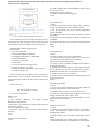
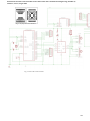
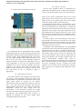
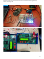
International Journal of Advanced Research in Electronics and Communication Engineering (IJARECE) Volume 3, Issue 8, August 2014 Simulation of On-board diagnostics in Automobiles using CAN Protocol Swathi Tangi, Anshuman Kumar, Chinmay Khandalkar Abstract— More than 70 ECUs are implemented in cars, and the number is still increasing. As a result, the complexity of automotive networks and cabling is extensive. In order to reduce the amount of wiring and diagnose wiring faults, the CAN bus may be used in vehicles to connect different ECUs.The main aim of the project is to simulate a working hardware model of a Vehicle monitoring System indicating temperature and fuel status via CAN protocol. The communication between two nodes i.e. the transmitter and the receiver is via CAN protocol. The Transmitter node controller is programmed to input the parameter values (Temperature, Pressure etc.) and the receiver node controller will in turn control the output actuators such as Displays. The sender microcontroller reads the two analog values and sends it to the receiver end displaying the status in the LCD, hence successfully implementing the CAN protocol. Index Terms—CAN, LCD, Sensor, Temperature. I. INTRODUCTION CAN bus (for controller area network) is a vehicle bus standard designed to allow microcontrollers and devices to communicate with each other within a vehicle without a host computer. CAN bus is a message-based protocol, designed specifically for automotive applications but now also used in other areas such as aerospace, maritime, industrial automation and medical equipment.[1] [5] Development of the CAN bus started originally in 1983 at Robert Bosch GmbH and was officially released in 1986 at the Society of Automotive Engineers (SAE). CAN bus is one of the five protocols used in On-board diagnostics (OBD-II) vehicle diagnostic standard. This standard has been mandatory for all cars and light trucks sold in the United Sates since 1996. CAN specification 2.0 describes the base frame format (using 11-bit CAN identifier) and the extended frame format (using 29-bit CAN Identifier). [4] The complexity of automotive networks and cabling is extensive. [2] We need to find ways to reduce the amount of wiring and diagnose wiring faults. The CAN bus may be used in vehicles to connect different ECUs such as engine, climate control, ABS (Anti-Lock Braking System), etc. Bus Manuscript received July 2014 Swathi Tangi Electrical & Electronics, Manipal Institute of Technology,. Manipal, India, Ph: +919538410461. Anshuman Kumar, Electrical & Electronics, Manipal Institute of Technology, Manipal, India, Ph: +919916881678 Chinmay Khandalkar, Electrical & Electronics, Manipal Institute of Technology, Manipal, India, Ph: +917795026512 architecture is one of the ways to keep the volume of cabling from becoming unmanageable. CAN protocol was Fig1: Wiring simplifications via CAN Bus implemented using two nodes. The sender node was set with the analog values of temperature and fuel. These values were converted to digital by the sender microcontroller ADC and sent to the receiver node via the CAN bus setup by the transceivers. The receiver node compared these digital values and accordingly sent the control signals to the LCD and the LED’s. II. CAN HARDWARE A. Building Blocks 1) Line ending is used to prevent interference in a bus topology. Waves that reach the end of an open line can be reflected back and cause interference with the actual signal or even cancel it completely. This happens because the traveling signal is not absorbed completely and can be resolved by matching the impedance. For CAN in particular this means the bus needs to end with a resistor of 120 ohm. This line ending is only needed twice: at the beginning of the bus and at the end. Not every node has this. 2) CAN transceiver is responsible for converting signal levels from the CAN bus to levels the controller can understand. It also has protective circuitry to protect the CAN controller. ADM3053 by Analog devices Specifications: 5V operation. High speed data rates up to 5Mbps. 20-led, wide body SOIC package. Operating temperature range: -40˚C to 85˚C.[11] 806 ISSN: 2278 – 909X All Rights Reserved © 2014 IJARECE International Journal of Advanced Research in Electronics and Communication Engineering (IJARECE) Volume 3, Issue 8, August 2014 2: Set the CLKPR (Clock Prescale Register) to 0x00. (Clock Division Factor of 1) 3: Mark Pin D1 as an output pin. 4: Enable the global interrupt triggering. 5: End. Fig 2: Building Blocks to hardware components 3) CAN controller receives incoming messages from the CAN transceiver, waits until all bits have arrived, does some error checking and acts as a buffer for the host processor. ATMEGA32M1-15AD by Atmel devices. Specifications: 8 bit microcontroller. AVR enhanced RISC architecture. Throughputs approaching 1 MIPS/MHz. Harvard architecture. 11-channel 10-bit ADC. 10-bit ADC. CAN 2.0 A/B with 6 message objects. Operating voltage: 2.7V-5.5V. Extended operating temperature: -40˚C to 125˚C. Automotive grade. [10] 4) Host processor/CPU is the brains of the CAN-node. It handles all the sensor or actuator data but does not know anything about the CAN protocol. That is the job of the CAN controller. 5) Sensor/Actuator III. SOFTWARE DEVELOPMENT A. Sender Code Algorithm Main Function 1: Start. 2: Store function definitions and global variable definitions in the header file. 3: Initialize the microcontroller, the analog-digital convertor and the CAN module. 4: Clear the data transmit buffer. 5: Infinite loop. (The rest of the program is determined by interrupts) 6: End. Microcontroller Initialization 1: Start. ADC Initialization 1: Start 2: Select the program pins ADC4, ADC6, ADC7, ADC10 by setting the appropriate bits of the ADMUX register 3: Set the appropriate bits of the second configuration register ADCSRA. 4: Set the appropriate bits of the third configuration register ADCSRB. 5: Set the bit of timer0 configuration registers, TCCR0A and TCCR0B. 6: Set the TCNT0 register to 0. (Stores the current state of the timer) 7: End. CAN Initialization 1: Start. 2: Perform software reset on the CAN Module. 3: Set the CAN timer prescaler register to 0. (Used to select the clock division factor for the CAN Module) 4: Reset each of the message objects. 5: Use the 3 registers CANBT1, CANBT2, and CANBT3 to set the baud rate timing. 6: Configure the CANGIE registers to select which interrupts can be generated. (In this case, the global CAN interrupt is enabled and the interrupt on a received CAN message) 7: Enable the process for CAN module. 8: Assign a separate Message Object and Message ID to each of the analog sensors. 9: Stop. ADC Interrupt Handler 1: Start. 2: Access the 8 most significant bits through ADCH by selecting left adjustment in the initialization. 3: If counter value exceeds 3, start a new conversion. 4: Load a new value into the ADMUX register to select a new analog channel based on the counter value. 5: Write a logical one to bit 1 of the TIFR0 register. (Prevents generation of new interrupts) 6: Stop. Message Transmission 1: Start. 2: While Loop: Wait for the message object to be available. 3: Set the CANPAGE register to access the particular Message Object (Mob). 4: Set the interrupt enable bits of the CANIE2 register for the MOB. 5: Reset all the flags of the status register CANSTMOB. 6: Set the data length and normal mode of the control register 807 International Journal of Advanced Research in Electronics and Communication Engineering (IJARECE) Volume 3, Issue 8, August 2014 CANCDMOB. 7: Load the addresses into the CANIDT1 and CANIDT2 registers. 8: Load the data into the MOB data buffers by writing to the CANMSG register. 9: Put the MOB in transmit mode. 10: End. CAN Interrupt Handler 1: Start 2: Check for the TXOK flag. (Means transmission was complete) 3: Disable the MOB. 4: Reset all the interrupt flags. 5: Reset the original CANPAGE value. 6: End. B. Receiver Code Algorithm Main Function 1: Start. 2: Store function definitions and global variable definitions in the header file. 3: Initialize the microcontroller, the digital-analog convertor and the CAN module. 4: Clear the data transmit buffer. 5: Initialize the Message Objects 0 and 1. 6: Infinite loop. (The rest of the program is determined by interrupts) 7: End. Microcontroller Initialization 1: Start. 2: Set the CLKPR (Clock Prescale Register) to 0x00. (Clock Division Factor of 1) 3: Enable the global interrupt triggering. 4: End. 8: Assign a separate Message Object and Message ID to each of the analog sensors. 9: Stop. CAN Interrupt Handler 1: Start. 2: Check if the interrupt generated was by an incoming message. 3: According to the length of the data of the incoming message, retain data from CANMSG. 4: Write the received data to DACH. (Starts the DA Conversion) 5: End. Set an MOB in receiving mode. 1: Start. 2: Write 0b11111111 to CANIDM1 register. (Selects the 8 most significant bits) 3: Write logical 0 to bits 7:5 of CANIDM2 register. (3 least significant bits will be ignored) 4: Write 10 to bits 7:6 of the CANCDMOB register to turn the MOB in receiving mode. 5: End. IV. CIRCUITS AND SCHEMATICS All the circuit schematics have been developed using EAGLE (Easily Applicable Graphical Layout Editor) software by CadSoft. Eagle was used to design the breakout board. The symbols for the ADM3053 and the ATMEGA32M1 were not in the standard eagle library, so it was designed personally. The process consisted of referring the datasheets for exact dimensions of the IC, pins, gaps between the pins along with creating linkages between the pins and their functions. DAC Initialization 1: Start. 2: Set the appropriate bits of the ADMUX register. 3: Set the appropriate bits of the ADCSRB register. (Same as ADC) 4: Configure the DAC using DACON register. 5: End. CAN Initialization 1: Start. 2: Perform software reset on the CAN Module. 3: Set the CAN timer prescaler register to 0. (Used to select the clock division factor for the CAN Module) 4: Reset each of the message objects. 5: Use the 3 registers CANBT1, CANBT2, and CANBT3 to set the baud rate timing. 6: Configure the CANGIE registers to select which interrupts can be generated. (In this case, the global CAN interrupt is enabled and the interrupt on a received CAN message) 7: Enable the process for CAN module. 808 ISSN: 2278 – 909X All Rights Reserved © 2014 IJARECE International Journal of Advanced Research in Electronics and Communication Engineering (IJARECE) Volume 3, Issue 8, August 2014 Fig 3: IC footprints and schematics. Fig 5: CAN receiver node schematic Fig 4: CAN sender node schematic 809 International Journal of Advanced Research in Electronics and Communication Engineering (IJARECE) Volume 3, Issue 8, August 2014 VII. RESULT ANALYSIS V. PROGRAMMING THE MICROCONTROLLER Fig 6:ISP Programming of AVR Microcontroller The ATMEGA32M1 was programmed using In-System Programming (ISP). This is done by writing the code in the flash memory of the microcontroller through the pins that are normally used for serial communication (ISP). These pins are: VCC, GND, /RESET, MOSI, MISO and SCK. To be able to do this, you need a serial programmer. Instead of buying one of these, an Arduino was programmed to act as a serial programmer. In this way, the computer program AVRdude can be used to send the assembly code of the program to the Arduino using USB. The Arduino then pushes the code onto the micro controller using the serial port. The wiring for this is visualized in figure 6. [6][7][8][12] The two input parameters taken in consideration are Temperature and the Fuel status. To detect the temperature we have used the temperature sensor and to detect the fuel status we have used a potentiometer which acts as a fuel gauge sensor as they are based on the same principle. The output consists of an indicator light and an LCD display continuously monitoring the status of the inputs. The fuel gauge sensor works as a potentiometer. As the fuel decreases the resistance increases and vice versa. Hence, this can be simulated using a potentiometer. To detect the temperature LM-35 sensor from NI is used and it checks the temperature of the engine. The safety temperature for the engine (Body Frame) is roughly around 100˚ C-105˚C. Since these values can’t be achieved, we have reduced this value to 70˚C for testing purposes which can be simulated using a solder iron. As shown in figure 7, the circuit comprises of two sets of microcontroller and transceiver. The left side is the sender node whereas the receiver node is placed on the right. All the input values are given to the sender node and the outputs are controlled by the receiver node. The displays in the AT89C51ED2 Kits were programmed to indicate the status of the fuel and temperature separately. The Fuel LCD has two states i.e. Normal and Reserve. The temperature LCD also consists of two stages, Safe and High. The indicator lights and the LCD’s are controlled by the receiver microcontroller which sends the signal after the sender microcontroller converts them to digital values. The receiver microcontroller compares these values to pre-determined variables (For temperature 0.65 volts and for fuel 2.5 volts) and sends the control signals to the LED’s and the LCD’s accordingly. The fig 7 indicates the normal condition of the LCD’S and the temperature indication LED’s lighting up in respond to high temperature of the solder iron. VI. PROGRAMMING THE LCD The AT89C51ED2 kit with integrated LCD was used for the display of the temperature and the fuel status. The AT89C51ED2 was programmed in assembly to detect a high signal which would be received by the receiver microcontroller when the temperature exceeds its limit. The pin 1.7 acts as the input port for this signal. The same was implemented for the fuel status. The sender microcontroller continuously checks the input voltage from the potentiometer. As the resistance increases, this voltage increases and the fuel indicator light present in the receiver end lights up. This simultaneously sends a signal to a different kit dedicated for fuel status display which accordingly displays the Fuel status. 810 ISSN: 2278 – 909X All Rights Reserved © 2014 IJARECE International Journal of Advanced Research in Electronics and Communication Engineering (IJARECE) Volume 3, Issue 8, August 2014 Fig 7:LCD Display and temperature LEDs 811 International Journal of Advanced Research in Electronics and Communication Engineering (IJARECE) Volume 3, Issue 8, August 2014 VIII. CONCLUSION The current automobile data-acquisition systems have become complex, due to which the cabling has increased resulting in extensive wiring. Due to introduction of electronic injection system and safety system such as ABS, the communication between the sensors and the ECU is very critical. This communication is achieved through various protocols and mainly by Controller Area Network Protocol which is one of the five standard protocols of the On-board diagnostics-II standard implemented in most of the cars. The circuit implemented can be designed on a PCB and a compact module of a node can be manufactured. Thus a complete CAN circuit can be implemented for an automobile with more number of nodes for each sensor. Recent development in CAN is the introduction of the CAN FD. This eradicates the problem of higher bandwidth requirement of the 29-bit identifier and has increased bit rate allowing faster flow of information between the sensor and the ECUs. The protocol was simulated on a short-scale basis comprising of two nodes with one as the sender and the other as the receiver node. The sender node is set with the analog values of temperature and fuel. These values are converted to digital by the sender microcontroller ADC and sent to the receiver node via the CAN bus setup by the transceivers. The receiver node compares these digital values and accordingly sends the control signals to the LCD and the LED’s. Swathi Tangi has obtained her B.Tech Degree in Electrical and Electronics Engineering from S.T.I.E.T College, Vizianagram in 2008, M.Tech (Power & Energy Systems) Degree from NITK Surathkal in 2010 and is presently serving Manipal Institute of Technology, Manipal as Assistant Professor in EEE Department. Her areas of interest are Power Quality, Power system Dynamics, Utility applications of power electronics (HVDC, SVC, FACTS), Lightning and nuclear EMP impact on power lines. Chinmay Khandalkar completed his B.E Electrical & Electronics from Manipal Institute of Technology, Manipal in 2014. He was the part of the official formula student team “Formula Manipal” of Manipal University which participated in Formula Student Germany, Hockenheimring and Formula Student Czech Republic, Hradec Kralove in 2013.His areas of interest are Automotive electronics and embedded systems. Anshuman Kumar completed his B.E Electrical & Electronics from Manipal Institute of Technology, Manipal in 2014. His areas of interests are Computer Networks, Embedded Systems, and Automotive Electronics. REFERENCES [1] S. Vijaylaksmi, “Vehicle Control System Implementation Using CAN Protocol”, International Journal of Advanced Research in Electrical, Electronics and Instrumentation Engineering, Volume 2, Issue 6, June 2013. [2] “A Gateway System for an Automotive System: LIN, CAN, and FlexRay”, The IEEE International Conference on Industrial Informatics (INDIN 2008), DCC, Daejeon, Korea, July 13-16, 2008. [3] Steve Corrigan, “Introduction to Controller Area Network”, Application Report SLOA101A- August 2002 – Revised July 2008. [4] Mike Blenderman, “CAN on the AVR”, Draft 1.2 prerelease. [5] “Controller Area Network Overview (CAN)”, White Paper, National Instruments. [6] “In System Programming(ISP) of the ATMEL AVR flash microcontroller family using the SPI programming interface”, AN101, Application Note, Equinox_Tech. [7]”Atmel AVR910”, Application Note, www.atmel.in [8] “Atmel AVR4027”, Application Note, www.atmel.in [9] “Atmel AVR322”, Application Note, www.atmel.in [10] Datasheet ATMega32M1 Automotive Summary, www.atmel.in [11] Datasheet ADM3053 Analog Devices, www.analog.com [12] “AVR-LibC user Manual-Savannah”, www.nongnu.org 812 ISSN: 2278 – 909X All Rights Reserved © 2014 IJARECE