Download Hitex LPC1850 Eval Board UserManual
Transcript
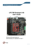
Board Description Version: 1.01 Involved Departments: R&D Board Description LPC1850EVA-A2 Evaluation Board Generated: 2011-09-26 Author: Ma Page 1 of 12 Board Description Version: 1.01 Involved Departments: R&D Page 2 of 12 Document management Document history Version 0.1 0.2 1.0 1.01 Status in progress Release Generated: 2011-09-26 Author: Ma Date 05.01.2011 27.04.2011 04.05.2011 15.09.2011 Responsible Ma Ma Ma Ma Reason for change New creation Changes to fit PCB Rev. –A2 Minor changes Minor changes Board Description Version: 1.01 Involved Departments: R&D Page 3 of 12 Purpose of the document This document describes the jumpers and connectors on the NXP LPC1850EVA-A2 evaluation board developed by Hitex. Authoring tools MS-Word Generated: 2011-09-26 Author: Ma Board Description Version: 1.01 Involved Departments: R&D Page 4 of 12 Contents 1 2 Overview ......................................................................................................................................... 5 Power............................................................................................................................................... 5 2.1 USB .......................................................................................................................................... 5 2.2 AC/DC Power Supply ............................................................................................................... 5 2.3 Power-over-Ethernet (PoE) ...................................................................................................... 5 3 Connectors ..................................................................................................................................... 6 4 Mutual Exclusive Functions ......................................................................................................... 7 4.1 Ethernet, SD Card .................................................................................................................... 7 4.2 CAN Interface, I2S (Audio) ...................................................................................................... 7 4.3 UART, Memories and UART-Bootloader ................................................................................. 7 4.4 Ext. LCD and ULPI ................................................................................................................... 7 4.5 USB0 ........................................................................................................................................ 7 4.6 USB1 ........................................................................................................................................ 7 4.7 Media Connector and Audio .................................................................................................... 8 4.8 SSP0 ........................................................................................................................................ 8 4.9 SPI............................................................................................................................................ 8 4.10 Default settings ........................................................................................................................ 9 5 Jumpers ........................................................................................................................................ 10 Related documents ............................................................................................................................ 12 Generated: 2011-09-26 Author: Ma Board Description Version: 1.01 Involved Departments: R&D Page 5 of 12 1 Overview The evaluation board has the following features: - CPU: LPC1850 (ARM Cortex-M3) - Power-over-Ethernet - Ready for energy consumption analysis with PowerScale of the complete board, the CPU-core and other peripherals - SDRAM, SRAM, parallel flash, NAND flash, qSPI flash - Temperature sensor, SD card, media-connector - CAN, UART, Ethernet, USB (Host, Device, OTG) - Debug with standard ARM JTAG and JTAG + Trace connector - Ready for Jennic ZigBee module - Small onboard display and NXP standard display / LCD interface - Touch buttons and LEDs - Wrap field for user circuits - Audio IN and OUT, microphone IN, headphones OUT and a D-Class amplifier - Ready for 4x ADC1415 analog-to-digital converters with user filtering option 2 Power 2.1 USB VBUS (+5V) can be supplied by either X13 or X2/X9. Please note that USB current is limited to 100mA. If the LPC1850 is running a program, which enumerates at the USB-Bus, the current limit can be set to 500mA (within that program) 2.2 AC/DC Power Supply A wall mount (or similar) AC/DC supply with 5V (DC) output can be connected to X14. Inner plug is positive, outer shell is negative. Jumper JP33 has to be set to pos 1-2. 2.3 Power-over-Ethernet (PoE) A Power-over-Ethernet module (U33) is populated on the evaluation board. Jumper JP33 has to be set to pos 2-3. Maximum output power of the module is 5V - 9W. Generated: 2011-09-26 Author: Ma Board Description Version: 1.01 Involved Departments: R&D Page 6 of 12 3 Connectors Designator X1 X2 X3 Function UART USB0 Media X4 JTAG X5 JTAG/Trace X6 X7 X8 SD Card CANopen D-Class amplifier X9 X10 X11 USB0 USB0 LCD X13 X14 USB1 Power X15 Ethernet/PoE LI1 Line In LI2 Line Out HP MIC Headphone Microphone Description D-SUB9 female connector for UART USB-B (device) connector This connector is to connect media devices like IPod and others with the Hitex Mediacable HK279. Please note: HK279 is not delivered within the LPC1850 evaluation board, but can be purchased separately at www.ehitex.de Shrouded connector for attaching a standard ARM debugger (2.54mm pitch, 20 pins) Connector for attaching an ARM Cortex-Debug+Trace debugger (1.27mm pitch, 20 pins) Not mounted SD card connector D-SUB9 male connector with CANopen pinout Screw connector for the D-Class amplifier output Pin Function 1 GND 2 OUTB 3 OUTA USB-microAB (OTG) connector USB-A (host) connector LCD connector for attaching an external LCD with NXP’s standard LCD interface USB-B (device) connector A wall mount (or similar) AC/DC supply with 5V (DC) output can be connected to X14. Inner plug is positive, outer shell is negative An Ethernet device for communication and/or a PSE device for powering the LPC1850 Evaluation Board can be connected to X15 Connector to the input amplifier of U10 When no plug is connected, the signal is automatically routed to connector X3 Connector from the output amplifier of U10 When no plug is connected, the signal is automatically routed to connector X3 Connector from the headphones output amplifier of U10 Connector to the microphone input amplifier of U10 SW1 SW2 SW4 Reset ISP Wakeup Global hardware reset Switch to pull EXTBUS_A9 low In combination with SV22 pins 7-8, pull WAKEUP0 low T1 T2 T3 T4 Touch1 Touch2 Touch3 Touch4 Touch button connected to U14 Touch button connected to U15 Touch button connected to U16 Touch button connected to U17 Generated: 2011-09-26 Author: Ma Board Description Version: 1.01 Involved Departments: R&D Page 7 of 12 4 Mutual Exclusive Functions In general, all signals with double names like “Ethernet/SD card” show that this signal is used in more than one function. 4.1 Ethernet, SD Card The Ethernet (MII) is multiplexed with the SD card interface (SDIO). Therefore jumper array SV3 and SV6 is used to connect ENET*-signals to the Ethernet PHY (U1) as well as jumper array SV12 connects SDIO*-signals to the SD card interface (X6). In the schematic the double used pins can be identified by their double name ENET_*/SDIO_*. Please note: The SD card connector is not populated and not supported by LPC1850 devices. 4.2 CAN Interface, I2S (Audio) The CAN interface is multiplexed with some I2S functionality. The audio outputs can’t be used when the CAN interface is used. Jumper array SV9 routes the I2S signals to the Audio-Codec UDA1380 (U10) and SV10 routes them to the D-Class amplifier (U19). Jumper array SV1 pins 1-2 and 3-4 connect the CAN transceiver (U7) to the signals. In the schematic the double used pins can be identified by their double name CAN1_TD/I2S_TX_SDA and CAN1_RD/I2S_TX_WS. 4.3 UART, Memories and UART-Bootloader The UART bootloader pins at the CPU are multiplexed with the external bus interface and so with all onboard memories. Also there is only one UART transceiver available (U6). At jumper array SV1 the user can set the jumpers to pins 5-6 and 7-8 for normal UART operation. If set to pins 9-10 and 11-12 the UART transceiver will be connected to signals EXTBUS_A13 and EXTBUS_A12. To avoid short circuit and damage to the CPU and UART transceiver, the user should not use the external bus interface while using UART bootloader on those pins. Please note: UART bootloader is not supported by the LPC1850 evaluation board. 4.4 Ext. LCD and ULPI The ULPI (USB1) interface is brought out to a pin-header for easier access. User should take care not to use these signals in parallel with the external LCD. 4.5 USB0 The USB0 functionality is brought out to a HOST (X10), a DEVICE (X2) and an OTG (X9) connector. Use only one connector at a time. 4.6 USB1 The USB1 functionality is brought out to a DEVICE (X13) connector. Also there is the option to connect the media connector X3 (USB lines) to the bus by closing jumper array SV28. Generated: 2011-09-26 Author: Ma Board Description Version: 1.01 4.7 Involved Departments: R&D Page 8 of 12 Media Connector and Audio If no 3,5mm audio plug is inserted into Audio IN (LINEIN1) or AUDIO OUT (LINEIN2), the corresponding signals of the audio codec (U10) will automatically connect to the media connector (X3). 4.8 SSP0 Signals SSP0_x are connected to Jennic ZigBee module (M1), to the internal LCD (LCD1), and to the fast ADCs (U11, U20, U21, U22). 4.9 SPI Signal SPI_SIO3 is connected to the qSPI device (U18) and to the I2C-EEPROM (U12). Use SV19 pins 1-2 or SV4 pins 9-10 to connect either to U12 or U18. Generated: 2011-09-26 Author: Ma Board Description Version: 1.01 Involved Departments: R&D Page 9 of 12 4.10 Default settings Jumper SV1 Function CAN UART UART bootloader SV3 and SV6 Ethernet (MII) SV4 SPI flash (qSPI) USB power UDA_RST Pin 3-4 I2S_TX* I2S_RX* I2C0* I2C0* I2S_TX* U11 SD card SV5 SV9 SV10 SV11 SV12 SV13 SV14 SV15 SV16 SV18 SV19 U20 U24 U21 U22 JENIC_RST SPI Pin 11 Pin 13 I2C0* SPI_SIO3 SV22 WAKEUP0 SV28 Media Connector USB Generated: 2011-09-26 Author: Ma Description Pin 1-2 and 3-4 are open No CAN interface (mutual exclusive to input-data of U10 and U19) Pin 5-6 and 7-8 are closed UART is connected to UART1 interface of the CPU Pin 9-10 and 11-12 are open The external bus interface is not available when using the UART bootloader. Please note: UART bootloader is not supported by the LPC1850 evaluation board. SV3 and SV6 are completely closed (pin 1-2, 3-4, etc.) Ethernet is available in MII-Mode Ethernet is mutual exclusive to SD card. SV4 is completely closed (pin 1-2, 3-4, etc.) Pin 9-10 is mutual exclusive to SV19 pin1-2 SV5 is completely closed (pin 1-2, 3-4, etc.) Pin 1-2 is closed, Reset of U10 Open, not connected Pins 5-6, 7-8, 9-10 are closed (mutual exclusive to CAN) Pins 11-12, 13-14, 15-16 are closed Pins 17-18, 19-20 are closed Pins 1-2, 3-4 are closed Pins 5-6, 7-8, 9-10 are closed (mutual exclusive to CAN) Signals for fast ADCs SV12 is open and is mutual exclusive to Ethernet Please note: The SD card connector is not populated and not supported by LPC1850 devices. Signals for fast ADCs Signals for fast ADCs Signals for fast ADCs Signals for fast ADCs Pin 15-16 is closed Pins 1-2, 3-4, 5-6, 7-8 are closed Pin 9-10 is open (jumper only set to one pin) SPISWP SPISSM Pins 3-4, 5-6 are closed EVENT# (output), pin 1-2 is open (jumper only set to one pin) Mutual exclusive to SV4 9-10 Pos 7-8 is closed Pos 1-2, 3-4, 5-6 are open Pos 1-2, 3-4, 5-6 are open (jumpers only set to one pin) Board Description Version: 1.01 Involved Departments: R&D Page 10 of 12 5 Jumpers Jumper JP1 Function R42 JP2 USB0_ID JP3 USB0_IND1 JP4 USB1_IND1 JP5 Boot control JP9 SD power JP10 LCD JP11 RTC JP15 GPIO_IRQ JP16 PowerScale JP17 DBGEN JP19 LCD JP20 LCD JP21 LCD JP22 LCD JP23 Write protect JP25 Write protect Generated: 2011-09-26 Author: Ma Description Connects R42 to GND when set to position 1-2 Default: pos. 1-2 Pulls USB0_ID permanently to GND Default: pos. 1-2 (closed) Connects USB0_IND1 to LED D10 Default: pos. 1-2 (closed) Connects ADC3_DAV to LED D9 Default: pos. 1-2 (closed) -tbd-, strapping option for the CPU Default: pos. 1 (open) Switches power to the SD card either by CPU (signals SDIO_POW) or permanently (position 1-2) Default: open Please note: The SD card connector is not populated and not supported by LPC1850 devices. Clock return from LCD Default: pos. 1 (open) With this jumper the CPU can set signal RTC_ALARM to power up or shut down its IO +3V3IO or the complete +3V3 power of the board. Default: pos. 1-2 Connects GPIO expander (U35) IRQ-signal to the CPU Default: pos. 1-2 (closed) At this point a Hitex PowerScale probe can be connected for current sensing the +3V3C (CPU Core power) and +3V3IO (CPU IO power) Default: pos. 1-2 (closed) -tbdDefault: pos. 1 (open) Switches signals LCDLE or permanently +3V3 to pin 29 of the external LCD Interface LCDLE = PWM or fixed signal from CPU +3V3 = Full brightness Default: pos. 1-2 LCDVDDEN -tbdDefault: pos. 1-2 (closed) Switches +5V to the LCD backlight Default: pos. 1-2 (closed) LCDVEEEN -tbdDefault: pos. 1-2 (closed) Write protect of parallel flash (U5) Default: pos. 1 (open) Write protect of NAND flash (U4) Default: pos. 1 (open) Board Description Version: 1.01 JP30 PowerScale JP31 PowerScale JP32 CAN 120R JP33 Power JP43 VBAT Generated: 2011-09-26 Author: Ma Involved Departments: R&D Page 11 of 12 At this point a Hitex PowerScale probe can be connected for current sensing of the whole board. Default: pos. 1-2 (closed) At this point a Hitex PowerScale probe can be connected for current sensing the +3V3 power. Default: pos. 1-2 (closed) Connects a 120OHM termination resistor to the CANH/CANL lines Default: pos. 1-2 (closed) Switches between Power-over-Ethernet or 5V wall plug for board supply. Default: pos. 1-2 Connects either a battery (not mounted) or +3V3C (Core power) to the VBAT pin of the CPU. Also hardware reset pullup R41 is connected to that power. Default: pos. 2-3 Board Description Version: 1.01 Involved Departments: R&D Related documents Schematics SCM_LPC1850EVA-A2-2.pdf, 2011-04-27 Assembly BPL_LPC1850EVA-A2-2.pdf, 2011-04-02 Generated: 2011-09-26 Author: Ma Page 12 of 12


