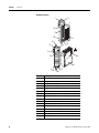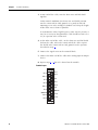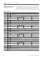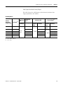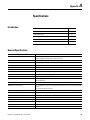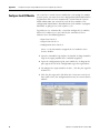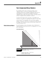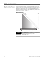
1
Compact I/O Combination Fast
Analog I/O Module
User Manual
(Catalog Number
1769-IF4FXOF2F)
Important User Information
Solid state equipment has operational characteristics differing from those of electromechanical equipment. Safety
Guidelines for the Application, Installation and Maintenance of Solid State Controls (publication SGI-1.1 available
from your local Rockwell Automation sales office or online at http://literature.rockwellautomation.com) describes
some important differences between solid state equipment and hard-wired electromechanical devices. Because of
this difference, and also because of the wide variety of uses for solid state equipment, all persons responsible for
applying this equipment must satisfy themselves that each intended application of this equipment is acceptable.
In no event will Rockwell Automation, Inc. be responsible or liable for indirect or consequential damages resulting
from the use or application of this equipment.
The examples and diagrams in this manual are included solely for illustrative purposes. Because of the many
variables and requirements associated with any particular installation, Rockwell Automation, Inc. cannot assume
responsibility or liability for actual use based on the examples and diagrams.
No patent liability is assumed by Rockwell Automation, Inc. with respect to use of information, circuits, equipment,
or software described in this manual.
Reproduction of the contents of this manual, in whole or in part, without written permission of Rockwell
Automation, Inc., is prohibited.
Throughout this manual, when necessary, we use notes to make you aware of safety considerations.
WARNING
IMPORTANT
ATTENTION
Identifies information about practices or circumstances that can cause an explosion in a
hazardous environment, which may lead to personal injury or death, property damage, or
economic loss.
Identifies information that is critical for successful application and understanding of the product.
Identifies information about practices or circumstances that can lead to personal injury or death,
property damage, or economic loss. Attentions help you identify a hazard, avoid a hazard, and
recognize the consequence
SHOCK HAZARD
Labels may be on or inside the equipment, for example, a drive or motor, to alert people that
dangerous voltage may be present.
BURN HAZARD
Labels may be on or inside the equipment, for example, a drive or motor, to alert people that
surfaces may reach dangerous temperatures.
Rockwell Automation, Allen-Bradley, TechConnect, CompactLogix, Compact I/O, MicroLogix, RSLogix 5000, RSLogix 500, RSNetWorx, RSNetWorx for DeviceNet, and RSLinx are trademarks of
Rockwell Automation, Inc.
Trademarks not belonging to Rockwell Automation are property of their respective companies.
Table of Contents
Preface
Introduction . . . . . . . . . . . . . . . .
About This Publication . . . . . . . .
Who Should Use This Publication
Additional Resources. . . . . . . . . .
.
.
.
.
.
.
.
.
.
.
.
.
.
.
.
.
.
.
.
.
.
.
.
.
.
.
.
.
.
.
.
.
.
.
.
.
.
.
.
.
.
.
.
.
.
.
.
.
.
.
.
.
.
.
.
.
.
.
.
.
.
.
.
.
.
.
.
.
.
.
.
.
.
.
.
.
.
.
.
.
.
.
.
.
7
7
7
8
.
.
.
.
.
.
.
.
.
.
.
.
.
.
.
.
.
.
.
.
.
.
.
.
.
.
.
.
.
.
.
.
.
.
.
.
.
.
.
.
.
.
.
.
.
.
.
.
.
.
.
.
.
.
.
.
.
.
.
.
.
.
.
.
.
.
.
.
.
.
.
.
.
.
.
.
.
.
.
.
. 9
. 9
11
11
Introduction . . . . . . . . . . . . . . . . . . . . . . . . . . . . . . . . . . . .
General Considerations . . . . . . . . . . . . . . . . . . . . . . . . . . . .
Hazardous Location Considerations . . . . . . . . . . . . . . . .
Prevent Electrostatic Discharge . . . . . . . . . . . . . . . . . . . .
Remove Power . . . . . . . . . . . . . . . . . . . . . . . . . . . . . . .
Reduce Noise . . . . . . . . . . . . . . . . . . . . . . . . . . . . . . . .
Protecting the Circuit Board from Contamination. . . . . . .
Assemble the Compact I/O System . . . . . . . . . . . . . . . . . . .
Mounting the Module . . . . . . . . . . . . . . . . . . . . . . . . . . . . .
Minimum Spacing . . . . . . . . . . . . . . . . . . . . . . . . . . . . .
Mount to a Panel . . . . . . . . . . . . . . . . . . . . . . . . . . . . . .
Mount to a DIN Rail. . . . . . . . . . . . . . . . . . . . . . . . . . . .
Replace a Single Module Within a System . . . . . . . . . . . . . .
Grounding the Module . . . . . . . . . . . . . . . . . . . . . . . . . . . .
System Wiring Guidelines . . . . . . . . . . . . . . . . . . . . . . . . . .
Effect of Transducer/Sensor and Cable Length Impedance
on Voltage Input and Output Accuracy. . . . . . . . . . . . . .
Label the Terminals. . . . . . . . . . . . . . . . . . . . . . . . . . . . . . .
Remove the Finger-safe Terminal Block . . . . . . . . . . . . . . . .
Wire the Finger-safe Terminal Block . . . . . . . . . . . . . . . . . .
Wire Size and Terminal Screw Torque . . . . . . . . . . . . . .
Wire the Modules . . . . . . . . . . . . . . . . . . . . . . . . . . . . . . . .
13
13
14
14
15
15
15
16
17
17
18
19
19
20
21
Chapter 1
Overview
Introduction . . . . . .
Module Description.
System Overview . .
Module Operation. .
.
.
.
.
.
.
.
.
.
.
.
.
.
.
.
.
.
.
.
.
.
.
.
.
.
.
.
.
.
.
.
.
.
.
.
.
.
.
.
.
Chapter 2
Installation and Wiring
22
24
25
25
26
27
Chapter 3
Module Data, Status, and Channel Introduction . . . . . . . . . . . . . . . . . . . . . . . . . . . . . . . . . . . . 33
Module Addressing . . . . . . . . . . . . . . . . . . . . . . . . . . . . . . . 34
Configuration
Input Image. . . . . . . . . . . . . . . . . . . . . . . . . . . . . . . . . . 34
Output Image . . . . . . . . . . . . . . . . . . . . . . . . . . . . . . . . 35
Configuration File . . . . . . . . . . . . . . . . . . . . . . . . . . . . . 35
3Publication 1769-UM019A-EN-P - October 2008
3
Table of Contents
Input Data File . . . . . . . . . . . . . . . . . . . . . . . . . . . . . . . .
Time Stamp Value (Word 4) . . . . . . . . . . . . . . . . . . . .
General Input Status Bits (SI0…SI3) . . . . . . . . . . . . . .
Low Alarm Flag Bits (LI0 …LI3) . . . . . . . . . . . . . . . . .
High Alarm Flag Bits (HI0…HI3) . . . . . . . . . . . . . . . .
Over-range Flag Bits (OI0…OI3) . . . . . . . . . . . . . . . .
Under-range Flag Bits (UI0…UI13) . . . . . . . . . . . . . . .
General Output Status Bits (SO0 and SO1) . . . . . . . . .
High Clamp (over-range) Flag Bits (OO0 and OO1) . .
Low Clamp (under-range) Flag Bits (UO0 and UO1) . .
Output Data File . . . . . . . . . . . . . . . . . . . . . . . . . . . . . . .
Cancel Input Alarm Control Bits (CLL0…CLL3 and
CLH0…CLH3) . . . . . . . . . . . . . . . . . . . . . . . . . . . . . .
Cancel Output Clamp Flag Control Bits (CLO0…CLO1
and CHO0…CHO1) . . . . . . . . . . . . . . . . . . . . . . . . . .
Configuration Data File . . . . . . . . . . . . . . . . . . . . . . . . . .
Input Channel Configuration . . . . . . . . . . . . . . . . . . . . . .
Enable/Disable Channel (EC) . . . . . . . . . . . . . . . . . . .
Input Filter Selection . . . . . . . . . . . . . . . . . . . . . . . . .
Input Type/Range Selection . . . . . . . . . . . . . . . . . . . .
Input Data Selection Formats . . . . . . . . . . . . . . . . . . .
Real Time Sampling . . . . . . . . . . . . . . . . . . . . . . . . . .
Time Stamping. . . . . . . . . . . . . . . . . . . . . . . . . . . . . .
Process Alarms . . . . . . . . . . . . . . . . . . . . . . . . . . . . .
Alarm Deadband . . . . . . . . . . . . . . . . . . . . . . . . . . . .
Output Channel Configuration. . . . . . . . . . . . . . . . . . . . .
Enable/Disable Channel (EC) . . . . . . . . . . . . . . . . . . .
Program Mode (PM). . . . . . . . . . . . . . . . . . . . . . . . . .
Program Value. . . . . . . . . . . . . . . . . . . . . . . . . . . . . .
Fault Mode (FM) . . . . . . . . . . . . . . . . . . . . . . . . . . . .
Fault Value . . . . . . . . . . . . . . . . . . . . . . . . . . . . . . . .
Program to Fault Enable (PFE) . . . . . . . . . . . . . . . . . .
Clamping (Limiting) . . . . . . . . . . . . . . . . . . . . . . . . . .
Clamp High and Clamp Low Data Values . . . . . . . . . .
Output Ramping . . . . . . . . . . . . . . . . . . . . . . . . . . . .
Output Type/Range Selection. . . . . . . . . . . . . . . . . . .
Output Data Selection Formats . . . . . . . . . . . . . . . . . .
.
.
.
.
.
.
.
.
.
.
.
.
.
.
.
.
.
.
.
.
.
.
36
36
36
37
37
37
37
38
38
38
39
. . 39
.
.
.
.
.
.
.
.
.
.
.
.
.
.
.
.
.
.
.
.
.
.
.
.
.
.
.
.
.
.
.
.
.
.
.
.
.
.
.
.
.
.
.
.
.
.
39
40
41
43
43
45
45
46
47
48
48
49
50
50
51
51
52
52
52
53
53
55
56
.
.
.
.
.
.
.
.
.
.
.
.
.
.
59
59
59
59
60
60
60
Chapter 4
Module Diagnostics and
Troubleshooting
4
Introduction . . . . . . . . . . . . . . . . . . . . . . . .
Safety Considerations . . . . . . . . . . . . . . . . .
Power Status Indicator . . . . . . . . . . . . . .
Activate Devices When Troubleshooting .
Stand Clear of the Machine. . . . . . . . . . .
Program Alteration. . . . . . . . . . . . . . . . .
Safety Circuits . . . . . . . . . . . . . . . . . . . .
.
.
.
.
.
.
.
.
.
.
.
.
.
.
.
.
.
.
.
.
.
.
.
.
.
.
.
.
.
.
.
.
.
.
.
.
.
.
.
.
.
.
.
.
.
.
.
.
.
.
.
.
.
.
.
.
.
.
.
.
.
.
.
.
.
.
.
.
.
.
Publication 1769-UM019A-EN-P - October 2008
Table of Contents
Power Cycle Diagnostics . . . . . . . . . . . . .
Channel Diagnostics . . . . . . . . . . . . . . . .
Out-of-range Detection . . . . . . . . . . .
Process Alarm Detection . . . . . . . . . .
Output Clamp Detection . . . . . . . . . .
Non-critical Versus Critical Module Errors.
Module Error Definition Table . . . . . . . . .
Module Error Field. . . . . . . . . . . . . . .
Extended Error Information Field . . . .
Error Codes . . . . . . . . . . . . . . . . . . . . . .
Invalid Input Range Selected . . . . . . .
Invalid Input Format Selected. . . . . . .
Alarm Not Enabled. . . . . . . . . . . . . . .
Invalid Alarm Data. . . . . . . . . . . . . . .
Invalid Input Filter Selected . . . . . . . .
Invalid Output Range Selected . . . . . .
Invalid Output Format Selected . . . . .
Invalid Fault Value Selected . . . . . . . .
Invalid Program/Idle Value Selected(1)
Invalid Clamp Value Selected . . . . . . .
Invalid Ramp Rate Selected . . . . . . . .
Invalid Real Time Sample Value . . . . .
Module Inhibit Function . . . . . . . . . . . . .
Contacting Rockwell Automation . . . . . . .
.
.
.
.
.
.
.
.
.
.
.
.
.
.
.
.
.
.
.
.
.
.
.
.
.
.
.
.
.
.
.
.
.
.
.
.
.
.
.
.
.
.
.
.
.
.
.
.
.
.
.
.
.
.
.
.
.
.
.
.
.
.
.
.
.
.
.
.
.
.
.
.
.
.
.
.
.
.
.
.
.
.
.
.
.
.
.
.
.
.
.
.
.
.
.
.
.
.
.
.
.
.
.
.
.
.
.
.
.
.
.
.
.
.
.
.
.
.
.
.
.
.
.
.
.
.
.
.
.
.
.
.
.
.
.
.
.
.
.
.
.
.
.
.
.
.
.
.
.
.
.
.
.
.
.
.
.
.
.
.
.
.
.
.
.
.
.
.
.
.
.
.
.
.
.
.
.
.
.
.
.
.
.
.
.
.
.
.
.
.
.
.
.
.
.
.
.
.
.
.
.
.
.
.
.
.
.
.
.
.
.
.
.
.
.
.
.
.
.
.
.
.
.
.
.
.
.
.
.
.
.
.
.
.
.
.
.
.
.
.
.
.
.
.
.
.
.
.
.
.
.
.
.
.
.
.
.
.
.
.
.
.
.
.
.
.
.
.
.
.
.
.
.
.
.
.
.
.
.
.
.
.
.
.
.
.
.
.
.
.
.
.
.
.
.
.
.
.
.
.
.
.
.
.
.
.
.
.
.
.
.
.
.
.
.
.
.
.
.
.
.
.
.
.
.
.
.
.
.
.
.
.
.
.
.
.
60
61
61
61
61
61
62
62
62
63
64
65
65
65
65
66
66
66
66
67
67
67
67
68
.
.
.
.
.
.
.
.
.
.
.
.
.
.
.
.
.
.
.
.
.
.
.
.
.
.
.
.
.
.
.
.
.
.
.
.
.
.
.
.
.
.
.
.
.
.
.
.
.
.
.
.
.
.
.
.
.
.
.
.
.
.
.
.
.
.
.
.
.
.
.
.
..
..
..
..
..
..
69
69
70
71
72
72
Introduction . . . . . . . . . . . . . . . . . . . . . . . . . . . . . .
Module Input Image . . . . . . . . . . . . . . . . . . . . . . . .
Module Output Image . . . . . . . . . . . . . . . . . . . . . . .
Module Configuration File . . . . . . . . . . . . . . . . . . . .
Configure Analog I/O Modules in a MicroLogix 1500
System . . . . . . . . . . . . . . . . . . . . . . . . . . . . . . . . . .
.
.
.
.
.
.
.
.
.
.
.
.
.
.
.
.
.
.
.
.
73
73
74
74
Appendix A
Specifications
Introduction . . . . . . . .
General Specifications .
Input Specifications. . .
Output Specifications .
Certifications. . . . . . . .
Replacement Parts. . . .
.
.
.
.
.
.
.
.
.
.
.
.
.
.
.
.
.
.
.
.
.
.
.
.
.
.
.
.
.
.
.
.
.
.
.
.
.
.
.
.
.
.
.
.
.
.
.
.
.
.
.
.
.
.
.
.
.
.
.
.
.
.
.
.
.
.
.
.
.
.
.
.
.
.
.
.
.
.
.
.
.
.
.
.
Appendix B
Module Addressing and
Configuration with MicroLogix
1500 Controller
Publication 1769-UM019A-EN-P - October 2008
.
.
.
.
. . . . . . 75
5
Table of Contents
Appendix C
Configuration Using the RSLogix
5000 Generic Profile for
CompactLogix Controllers
Introduction . . . . . . . . . . . . . . . . . . . . . . . . . . . . . . . . . . . . 79
Add the Module to Your Project . . . . . . . . . . . . . . . . . . . . . 79
Configure Each I/O Module. . . . . . . . . . . . . . . . . . . . . . . . . 82
Appendix D
Two’s Complement Binary
Numbers
Positive Decimal Values . . . . . . . . . . . . . . . . . . . . . . . . . . . 83
Negative Decimal Values . . . . . . . . . . . . . . . . . . . . . . . . . . . 84
Glossary
Index
6
Publication 1769-UM019A-EN-P - October 2008
Preface
Introduction
Read this preface to familiarize yourself with the rest of the manual.
Topic
About This Publication
Page
About This Publication
7
Who Should Use This Publication
7
Additional Resources
8
This manual is a guide for using the Compact I/O Combination Fast
Analog I/O Module, catalog number 1769-IF4FXOF2F. It describes the
procedures you use to configure, operate, and troubleshoot your
module.
For detailed information on related topics like programming your
CompactLogix or MicroLogix controller, or DeviceNet adapter, or for
information on CompactLogix components, see the list of Additional
Resources on page 8.
Who Should Use This
Publication
7Publication 1769-UM019A-EN-P - October 2008
Use this manual if you are responsible for designing, installing,
programming, or troubleshooting control systems that use Compact
I/O modules.
7
Preface
Additional Resources
These documents contain additional information about control
systems that use Compact I/O modules.
Resource
Description
MicroLogix 1500 User Manual, publication 1764-UM001
A user manual containing information on how to install, use, and
program your MicroLogix 1500 controller.
DeviceNet Adapter User Manual, publication 1769-UM001
A user manual containing information on how to install and use your
1769-ADN DeviceNet adapter.
CompactLogix System User Manual, publication 1769-UM007
A user manual containing information on how to install, use, and
program your 1769-L20 and 1769-L30 CompactLogix controllers.
CompactLogix Controllers User Manual, publication 1769-UM011 A user manual containing information on how to install, use, and
program your 1769-L31, 1769-L32C, 1769-L32E, 1769-L35CR, and
1769-L35E CompactLogix controllers.
Compact I/O Selection Guide, publication 1769-SG002
An overview of 1769 Compact I/O modules.
MicroLogix Programmable Controllers Selection Guide,
publication 1761-SG001
An overview of the MicroLogix 1500 System, including the 1769
Compact I/O system.
Industrial Automation Wiring and Grounding Guidelines,
publication 1770-4.1
In-depth information on grounding and wiring Allen-Bradley
programmable controllers.
You can view or download publications at
http://literature.rockwellautomation.com. To order paper copies of
technical documentation, contact your local Rockwell Automation
distributor or sales representative.
8
Publication 1769-UM019A-EN-P - October 2008
Chapter
1
Overview
Introduction
Topic
Module Description
Page
Module Description
9
System Overview
11
Module Operation
11
The module converts and digitally stores analog data for retrieval by
controllers, such as the CompactLogix or MicroLogix 1500 controllers.
The module also converts digital data from controllers to provide
analog output data. The module provides the following input and
output types and ranges.
Normal and Full Ranges
Signal Type
Voltage
Current
Normal Operating Input Range
Full Module Range
±10V DC
± 10.5V DC
1…5V DC
0.5…5.25V DC
0…5V DC
-0.5…5.25V DC
0…10V DC
-0.5…10.5V DC
0…20 mA
0…21 mA
4…20 mA
3.2…21 mA
The data can be configured as:
•
•
•
•
engineering units.
scaled-for-PID.
percent range.
raw/proportional data.
Module configuration is normally done via the controller’s
programming software. In addition, some controllers support
configuration via the user program. In either case, the module
configuration is stored in the memory of the controller. Refer to your
controller’s user manual for more information.
9Publication 1769-UM019A-EN-P - October 2008
9
Chapter 1
Overview
Hardware Features
2a
1
3
OK
Analog
DANGER
Do Not Remove RTB Under Power
Unless Area is Non-Hazardous
10a
V in 0 +
V in 1+
V/I in 1I in 1+
V/I in 0I in 0 +
V in 2+
V in 3+
10
V/I in 2 V/I in 3I in 2+
I in 3 +
ANLG
Com
ANLG
Com
V out 0+
10b
V out 1+
I out 0+
I out 1+
Ensure Adjacent
Bus Lever is Unlatched/Latched
Before/After
Removing/Inserting Module
4
1769-IF4FXOF2F
8a
7a
7a
2b
OK
Analog
5a
5b
9
6
7b
10
8b
7b
Item
Description
1
Bus lever (with locking function)
2a
Upper-panel mounting tab
2b
Lower-panel mounting tab
3
Module status indicators
4
Module door with terminal identification label
5a
Movable bus connector with female pins
5b
Stationary bus connector with male pins
6
Nameplate label
7a
Upper tongue-and-groove slots
7b
Lower tongue-and-groove slots
8a
Upper DIN-rail latch
8b
Lower DIN-rail latch
9
Write-on label for user identification tags
10
Removable terminal block (RTB) with finger-safe cover
10a
RTB retaining screw
10b
RTB retaining screw
Publication 1769-UM019A-EN-P - October 2008
Overview
System Overview
Chapter 1
The module communicates to the controller through the bus interface.
The module also receives 5 and 24V DC power through the bus
interface.
You can install as many analog modules as your power supply can
support. However, the modules may not be located more than eight
modules away from the system power supply.
1
2
3
End Cap
1
Compact I/O
2
Compact I/O
3
Compact I/O
Compact I/O
System Power Supply
Compact I/O
4
Compact I/O
CompactLogix Controller
or I/O Communication
Adapter
Determine Power Supply Distance
Power Supply Distance
Module Operation
Compact I/O
Compact I/O
Compact I/O
End Cap
MicroLogix 1500 Controller
with Integrated System
Power Supply
Compact I/O
or
1
2
3
4
Power Supply Distance
When you cycle power, the module performs a check of its internal
circuits, memory, and basic functions. During this time, the
module-status OK indicator remains off. If no faults are found during
power-cycle diagnostics, the module-status OK indicator is turned on.
After power-cycle checks are complete, the module waits for valid
channel-configuration data. If an invalid configuration is detected, the
module generates a configuration error. Once a channel is properly
configured and enabled, the module begins its conversion process.
Each time an input channel is read, the converted analog data value is
tested for an over-range or under-range condition. In addition, the
module supports user-configured high and low alarm condition tests
for each input channel. If any of these conditions are detected, unique
bits are set in the input-channel status word.
Publication 1769-UM019A-EN-P - October 2008
11
Chapter 1
Overview
Each time a new output value is sent to the module, it is tested for an
over-range or under-range condition. In addition, the module
supports user-configured high and low output clamps for each output
channel. If any of these conditions are detected, unique bits are set in
the output-channel status word.
The channel status words are described in the Input Data File on
page 36.
The controller uses two’s complement binary data when
communicating with the module. This typically occurs at the end of
the program scan or when commanded by the control program. If the
controller and the module determine that the bus data transfer was
made without error, the input data is used in your control program
and the output data is used by the module.
No field calibration is required.
12
Publication 1769-UM019A-EN-P - October 2008
Chapter
2
Installation and Wiring
Introduction
Topic
General Considerations
Page
General Considerations
13
Assemble the Compact I/O System
16
Mounting the Module
17
Replace a Single Module Within a System
19
Grounding the Module
20
System Wiring Guidelines
21
Label the Terminals
24
Remove the Finger-safe Terminal Block
25
Wire the Finger-safe Terminal Block
25
Wire the Modules
27
The Compact I/O system is suitable for use in an industrial
environment when installed in accordance with these instructions.
Specifically, this equipment is intended for use in clean, dry
environments (Pollution degree 2(1)) and to circuits not exceeding
Over Voltage Category II(2) (IEC 60664-1).(3)
(1) Pollution Degree 2 is an environment where, normally, only non-conductive pollution occurs except that
occasionally a temporary conductivity caused by condensation shall be expected.
(2) Over Voltage Category II is the load level section of the electrical distribution system. At this level, transient
voltages are controlled and do not exceed the impulse voltage capability of the product’s insulation.
(3) Pollution Degree 2 and Over Voltage Category II are International Electrotechnical Commission (IEC)
designations.
13Publication 1769-UM019A-EN-P - October 2008
13
Chapter 2
Installation and Wiring
Hazardous Location Considerations
This equipment is suitable for use in Class I, Division 2, Groups A, B,
C, D or nonhazardous locations only. The following attention
statement applies to use in hazardous locations.
ATTENTION
EXPLOSION HAZARD
• Substitution of components may impair suitability for Class I,
Division 2.
• Do not replace components or disconnect equipment unless
power has been switched off or the area is known to be
nonhazardous.
• Do not connect or disconnect components unless power has
been switched off or the area is known to be nonhazardous.
• This product must be installed in an enclosure.
• All wiring must comply with N.E.C. article 501-4(b).
Prevent Electrostatic Discharge
ATTENTION
Electrostatic discharge can damage integrated circuits or
semiconductors if you touch analog I/O module bus-connector pins
or the terminal block on the input module. Follow these guidelines
when you handle the module:
•
•
•
•
•
•
14
Touch a grounded object to discharge static potential.
Wear an approved wrist-strap grounding device.
Do not touch the bus connector or connector pins.
Do not touch circuit components inside the module.
Use a static-safe work station, if available.
Keep the module in its static-shield box, when it is not in use.
Publication 1769-UM019A-EN-P - October 2008
Installation and Wiring
Chapter 2
Remove Power
ATTENTION
Remove power before removing or inserting this module. When
you remove or insert a module with power applied, an electrical
arc may occur. An electrical arc can cause personal injury or
property damage by:
• sending an erroneous signal to your system’s field devices,
causing unintended machine motion.
• causing an explosion in a hazardous environment.
Electrical arcing causes excessive wear to contacts on both the
module and its mating connector and may lead to premature
failure.
Reduce Noise
Most applications require installation in an industrial enclosure to
reduce the effects of electrical interference. Analog inputs and outputs
are highly susceptible to electrical noise. Electrical noise coupled to
the analog inputs and outputs reduces the performance (accuracy) of
the module.
Group your modules to minimize adverse effects from radiated
electrical noise and heat. Consider the following conditions when
selecting a location for the analog module. Position the module:
• away from sources of electrical noise such as hard-contact
switches, relays, and AC motor drives.
• away from modules that generate significant radiated heat, such
as the 1769-IA16 module. Refer to the module’s heat dissipation
specification.
In addition, route shielded, twisted-pair analog input wiring away
from any high-voltage I/O wiring.
Protecting the Circuit Board from Contamination
The printed circuit board of the module must be protected from dirt,
oil, moisture, and other airborne contaminants. To protect the board,
the system must be installed in an enclosure suitable for the
environment. The interior of the enclosure should be kept clean and
the enclosure door should be kept closed whenever possible.
Publication 1769-UM019A-EN-P - October 2008
15
Chapter 2
Installation and Wiring
Assemble the Compact I/O
System
The module can be attached to the controller or an adjacent I/O
module before or after mounting.
For mounting instructions, see Panel Mounting By Using the
Dimensional Template on page 18, or Mount to a DIN Rail on page
19. To work with a system that is already mounted, see Replace a
Single Module Within a System on page 19.
3
4
2
1
6
1
5
1. Disconnect power.
2. Check that the bus lever of the module to be installed is in the
unlocked (fully right) position.
3. Use the upper and lower tongue-and-groove slots (1) to secure
the modules together (or to a controller).
4. Move the module back along the tongue-and-groove slots until
the bus connectors (2) line up with each other.
5. Use your fingers or a small screwdriver to push the bus lever
back slightly to clear the positioning tab (3).
16
Publication 1769-UM019A-EN-P - October 2008
Installation and Wiring
Chapter 2
6. To allow communication between the controller and module,
move the bus lever fully to the left (4) until it clicks.
Make sure it is locked firmly in place.
ATTENTION
When attaching I/O modules, it is very important that
the bus connectors are securely locked together to be
sure of proper electrical connection.
7. Attach an end cap terminator (5) to the last module in the
system by using the tongue-and-groove slots as before.
8. Lock the end cap bus terminator (6).
IMPORTANT
Mounting the Module
A 1769-ECR or 1769-ECL right or left end cap must be used to
terminate the end of the bus.
Modules may be mounted to a panel or to a DIN rail.
ATTENTION
During panel or DIN rail mounting of all devices, be sure that all
debris (that is, metal chips or wire strands) is kept from falling
into the module. Debris that falls into the module could cause
damage when you cycle power.
Minimum Spacing
Maintain spacing from enclosure walls, wireways, or adjacent
equipment. Allow 50 mm (2 in.) of space on all sides for adequate
ventilation.
Space Requirements
End Cap
Compact I/O
Compact I/O
Compact I/O
Side
Compact I/O
Host Controller
Compact I/O
Top
Side
Bottom
Publication 1769-UM019A-EN-P - October 2008
17
Chapter 2
Installation and Wiring
Mount to a Panel
Mount the module to a panel by using two screws per module. Use
M4 or #8 panhead screws. Mounting screws are required on every
module.
Panel Mounting By Using the Dimensional Template
Locate holes every 17.5 mm (0.689 in.) to allow for a mix of
single-wide and one-and-a-half-wide modules (for example, the
1769-OA16 module).
Overall hole spacing tolerance:
±0.4 mm (0.016 in.).
Host Controller
Spacing for single-wide modules 35 mm (1.378 in.).
l Mounting
Spacing for one-and-a-half-wide
modules 52.5 mm (2.067 in.).
Refer to host controller documentation for this dimension.
Panel Mounting By Using the Modules as a Template
This procedure lets you use the assembled modules as a template for
drilling holes in the panel. If you have sophisticated panel-mounting
equipment, you can use the dimensional template provided. Due to
module mounting-hole tolerance, it is important to follow these
procedures.
1. On a clean work surface, assemble no more than three modules.
2. Using the assembled modules as a template, carefully mark the
center of all module-mounting holes on the panel.
3. Return the assembled modules to the clean work surface,
including any previously mounted modules.
4. Drill and tap the mounting holes for the recommended M4 or #8
screw.
5. Place the modules back on the panel, and check for proper hole
alignment.
18
Publication 1769-UM019A-EN-P - October 2008
Installation and Wiring
Chapter 2
6. Attach the modules to the panel by using the mounting screws.
TIP
If mounting more modules, mount only the last one of this group
and put the others aside. This reduces remounting time during
drilling and tapping of the next group.
7. Repeat steps 1…6 for any remaining modules.
Mount to a DIN Rail
The module can be mounted by using the following DIN rails:
• 35 x 7.5 mm (EN 50 022 - 35 x 7.5)
• 35 x 15 mm (EN 50 022 - 35 x 15).
Before mounting the module on a DIN rail, close the DIN rail latches.
Press the DIN-rail mounting area of the module against the DIN rail.
The latches will momentarily open and lock into place.
Replace a Single Module
Within a System
The module can be replaced while the system is mounted to a panel
(or DIN rail). Follow these steps in order.
1. Remove power.
ATTENTION
Remove power before removing or inserting this module. When
you remove or insert a module with power applied, an electrical
arc may occur. An electrical arc can cause personal injury or
property damage by:
•sending an erroneous signal to your system’s field devices,
causing unintended machine motion.
•causing an explosion in a hazardous environment.
Electrical arcing causes excessive wear to contacts on both the
module and its mating connector and may lead to premature
failure.
2. On the module to be removed, remove the upper and lower
mounting screws from the module or open the DIN latches by
using a flat-blade or Phillips screwdriver.
3. Move the bus lever to the right to disconnect (unlock) the bus.
Publication 1769-UM019A-EN-P - October 2008
19
Chapter 2
Installation and Wiring
4. On the right-side adjacent module, move its bus lever to the
right (unlock) to disconnect it from the module to be removed.
5. Gently slide the disconnected module forward.
If you feel excessive resistance, check that the module has been
disconnected from the bus, and that both mounting screws have
been removed or DIN latches opened.
TIP
It may be necessary to rock the module slightly
from front to back to remove it, or, in a
panel-mounted system, to loosen the screws of
adjacent modules.
6. Before installing the replacement module, be sure that the bus
lever on the module to be installed and on the right-side
adjacent module are in the unlocked (fully right) position.
7. Slide the replacement module into the open slot.
8. Connect the modules together by locking (fully left) the bus
levers on the replacement module and the right-side adjacent
module.
9. Replace the mounting screws or snap the module onto the DIN
rail.
Grounding the Module
20
This product is intended to be mounted to a well-grounded mounting
surface, such as a metal panel. Additional grounding connections from
the module’s mounting tabs or DIN rail (if used) are not required
unless the mounting surface cannot be grounded. Refer to Industrial
Automation Wiring and Grounding Guidelines, publication 1770-4.1,
for additional information.
Publication 1769-UM019A-EN-P - October 2008
Installation and Wiring
System Wiring Guidelines
Chapter 2
Consider the following when wiring your system:
• All module commons (ANLG Com) are connected in the analog
module.
• The analog common (ANLG Com) is not connected to earth
ground inside the module.
• Channels are not isolated from each other.
• For optimum accuracy, limit overall cable impedance by
keeping your cable as short as possible. Locate the I/O system
as close to your sensors or actuators as your application will
permit.
• Use Belden 8761, or equivalent, shielded wire.
• Under normal conditions, the drain wire and shield junction
must be connected to earth ground via a panel or DIN rail
mounting screw at the analog I/O module end.(1) Keep shield
connection to ground as short as possible.
• If multiple power supplies are used with analog inputs, the
power supply commons must be connected.
• The module does not provide loop power for analog inputs. Use
a Class 2 power supply that matches the input transmitter
specifications.
• Differential analog inputs are more immune to noise than
single-ended analog inputs.
• Voltage outputs (Vout 0+ and Vout 1+) of the 1769-IF4FXOF2F
module are referenced to ANLG Com. Load resistance for a
voltage output channel must be equal to or greater than 1 kΩ .
• Current outputs (Iout 0+ and Iout 1+) of the 1769-IF4FXOF2F
module source current that returns to ANLG Com. Load
resistance for a current output channel must remain between 0
and 500 Ω .
• Voltages on Vin+, V/Iin-, and Iin+ terminals of the
1769-IF4FXOF2F module must be within ±10V DC of analog
common (ANLG Com).
(1) In environments where high-frequency noise may be present, it may be necessary to directly ground cable
shields to earth at the module end and via a 0.1 µF capacitor at the sensor end.
Publication 1769-UM019A-EN-P - October 2008
21
Chapter 2
Installation and Wiring
Effect of Transducer/Sensor and Cable Length Impedance on
Voltage Input and Output Accuracy
For voltage inputs and outputs, the length of the cable used between
the transducer/sensor/load and the module can affect the accuracy of
the data provided by the module.
Voltage Input Accuracy
Rs
Rc
+
Vs
V in
Ri
-
Rc
Where:
Rc = DC resistance of the cable (each conductor) depending on
cable length
Rs = Source impedance of analog transducer/sensor input
Ri = Impedance of the voltage input (220 kΩ)
Vs = Voltage source (voltage at the transducer/sensor input device)
Vin = Measured potential at the module input
%Ai = Percent added inaccuracy in a voltage-based system due
to source and cable impedance
[ Ri × Vs]
Vin = -------------------------------------------------------[ Rs + ( 2 × Rc ) + Ri ]
For example, for Belden 8761 two conductor, shielded cable:
Rc = 5.25 Ω/1000 m
Vin
% Ai = ⎛ 1 – ---------⎞ × 100
Rs = 0 (ideal source)
⎝
Vs ⎠
Effect of Cable Length on Input Accuracy
22
Length of Cable,
m (ft)
DC Resistance of the Cable,
Rc (Ω)
Accuracy Impact at the
Input Module
50 (164)
2.625
0.002385%
100 (328)
5.25
0.00477%
200 (656)
10.50
0.00954%
300 (984)
15.75
0.01431%
Publication 1769-UM019A-EN-P - October 2008
Installation and Wiring
Chapter 2
As input source impedance (Rs) and/or resistance (DC) of the cable
(Rc) get larger, system accuracy decreases. If you determine that the
inaccuracy error is significant, implementing the following equation in
the control program can compensate for the added inaccuracy error
due to the impedance of the source and cable.
[ Rs + ( 2 × Rc ) + Ri ]
Vs = Vin × -------------------------------------------------------Ri
For current signals, source and cable impedance do not impact
system accuracy.
TIP
Voltage Output Accuracy
Rs
Rc
+
Vs
V in
Ri
-
Rc
Where:
Rc = DC resistance of the cable (each conductor)
depending on cable length
Rs = Source impedance (1 Ω)
Ri = Impedance of the voltage input
Vs = Voltage at the output of 1769-IF4FXOF2F module
Vin = Measured potential at the module input
%Ai = Percent added inaccuracy in a voltage-based
system due to source and cable impedance
[ Ri × Vs]
Vin = -------------------------------------------------------[ Rs + ( 2 × Rc ) + Ri ]
Publication 1769-UM019A-EN-P - October 2008
23
Chapter 2
Installation and Wiring
For example, for Belden 8761 two conductor, shielded cable and a
1769-IF4 input module:
Rc = 52.5 Ω/1000 m
Rs = 1 Ω
Ri = 220 KΩ
Vin
% Ai = ⎛ 1 – ---------⎞ × 100
⎝
Vs ⎠
Effect of Output Impedance and Cable Length on Accuracy
Length of Cable
DC Resistance of the Cable Rc
Accuracy Impact at the
Input Module
50 m (164 ft)
2.625 Ω
0.00284%
100 m (328 ft)
5.25 Ω
0.00523%
200 m (656 ft)
10.50 Ω
0.01%
300 m (984 ft)
15.75 Ω
0.01477%
As output impedance (Rs) and/or resistance (DC) of the cable (Rc) get
larger, system accuracy decreases. If you determine that the
inaccuracy error is significant, implementing the following equation in
the control program can compensate for the added inaccuracy error
due to the impedance of the module’s voltage outputs and cable.
TIP
For current outputs, source and cable impedance do not impact
system accuracy as long as the total resistance of the cable and
input impedance of the load remain within the specified
maximum limits for the module's current outputs.
[ Rs + ( 2 × Rc ) + Ri ]
Vs = Vin × -------------------------------------------------------Ri
Label the Terminals
24
A removable, write-on label is provided with the module. Remove the
label from the door, mark the identification of each terminal with
permanent ink, and slide the label back into the door. Your markings
(ID tag) will be visible when the module door is closed.
Publication 1769-UM019A-EN-P - October 2008
Installation and Wiring
Remove the Finger-safe
Terminal Block
Chapter 2
When wiring field devices to the module, it is not necessary to remove
the terminal block. If you remove the terminal block, use the write-on
label on the side of the terminal block to identify the module slot
location and type. RTB position (for one-and-a-half size modules) can
be indicated by circling either the R for right side or L for left side.
Finger-safe Terminal Block
R SLOT # ____ L
MODULE TYPE _____ RoHS
To remove the terminal block, loosen the upper and lower retaining
screws. The terminal block will back away from the module as you
remove the screws. When replacing the terminal block, torque the
retaining screws to 0.46 N•m (4.1 lb•in).
Wire the Finger-safe
Terminal Block
Upper Retaining Screw
Lower Retaining Screw
When wiring the terminal block, keep the finger-safe cover in place.
1. Loosen the terminal screws to be wired.
2. Begin wiring at the bottom of the terminal block and move up.
Publication 1769-UM019A-EN-P - October 2008
25
Chapter 2
Installation and Wiring
3. Route the wire under the terminal pressure plate.
You can use the bare wire or a spade lug. The terminals accept a
6.35 mm (0.25 in.) spade lug.
TIP
The terminal screws are non-captive. Therefore, it is possible to
use a ring lug (maximum 1/4 in. o.d. with a 0.139 in. minimum
i.d. (M3.5)) with the module.
4. Tighten the terminal screw making sure the pressure plate
secures the wire.
Recommended torque when tightening terminal screws is
0.68 N•m (6 lb•in).
TIP
If you need to remove the finger-safe cover, insert a screwdriver
into one of the square, wiring holes and gently pry the cover off.
If you wire the terminal block with the finger-safe cover
removed, you will not be able to put it back on the terminal
block because the wires will be in the way.
Wire Size and Terminal Screw Torque
Each terminal accepts up to two wires.
Wire Type
Wire Size
Terminal Screw Torque
Retaining Screw Torque
Solid
Cu-90 °C (194 °F)
0.325…2.080 mm
2 (22…14 AWG)
0.68 N•m (6 lb•in)
0.46 N•m (4.1 lb•in)
Stranded
Cu-90 °C (194 °F)
0.325…1.310 mm2 (22…16 AWG)
0.68 N•m (6 lb•in)
0.46 N•m (4.1 lb•in)
26
Publication 1769-UM019A-EN-P - October 2008
Installation and Wiring
Chapter 2
Wire the Modules
ATTENTION
To prevent shock hazard, care should be taken when wiring the
module to analog signal sources. Before wiring any analog
module, disconnect power from the system power supply and
from any other source to the analog module.
After the analog module is properly installed, follow the wiring
procedure below. For proper operation and high immunity to
electrical noise, always use Belden 8761 (shielded, twisted-pair) or
equivalent wire.
ATTENTION
When wiring an analog input, take care to avoid connecting a
voltage source to a channel configured for current input.
Improper module operation or damage to the voltage source
can occur.
Never connect a voltage or current source to an analog output
channel.
Belden 8761 Wire
Cable
Cut foil shield
and drain wire.
Signal Wire
Signal Wire
Drain Wire
Foil Shield
Signal Wire
Signal Wire
To wire your module, follow these steps.
1. At each end of the cable, strip some casing to expose the
individual wires.
2. Trim the signal wires to 2-in. lengths.
3. Strip about 5 mm (3/16 in.) of insulation away to expose the end
of the wire.
ATTENTION
Publication 1769-UM019A-EN-P - October 2008
Be careful when stripping wires. Wire fragments that
fall into a module could cause damage when you cycle
power.
27
Chapter 2
Installation and Wiring
4. At one end of the cable, twist the drain wire and foil shield
together.
Under normal conditions, this drain wire and shield junction
must be connected to earth ground, via a panel or DIN rail
mounting screw at the analog I/O module end. Keep the length
of the drain wire as short as possible.
In environments where high frequency noise may be present, it
may be necessary to also ground the cable shields to earth via a
0.1 µF capacitor at the sensor end.
5. At the other end of the cable, cut the drain wire and foil shield
back to the cable, unless the sensor end of the cable requires
the shields to be connected to earth ground via the capacitor
described in step 4.
6. Connect the signal wires to the terminal block.
7. Connect the other end of the cable to the analog input or output
device.
8. Repeat steps 1…6 for each channel on the module.
Terminal Layout
V in 1+
V in 0+
V/I in 0-
V/I in 1 I in 1+
V in 3+
V/I in 3 -
I in 0+
V in 2 +
V/I in 2I in 2+
I in 3+
ANLG Com
V out 1+
I out 1+
28
ANLG Com
V out 0+
I out 0+
Publication 1769-UM019A-EN-P - October 2008
Installation and Wiring
Chapter 2
Wire Differential Inputs
Belden 8761 Cable (or equivalent)
V in 1+
+
V in 0+
V/I in 0-
V/I in 1 I in 1+
V in 3+
V/I in 3 -
V in 2 +
V/I in 2I in 2+
I in 3+
ANLG Com
V out 1+
I out 1+
Differential
Current
Transmitter (1)
–
I in 0+
Differential
Voltage
Transmitter (1)
Earth Ground the
Shield Locally at
the Module
ANLG Com
V out 0+
I out 0+
+
–
(1) The sensor power supply must be rated Class 2.
Earth Ground the Shield
Locally at the Module
Wiring Single-ended Sensor/Transmitter Types
Sensor/
+
Transmitter Power Supply(1)
Terminal Block
Current
Transmitter
+ Signal
V in 0+
I in 0+
V/I in 0 V in 1+
I in 1+
Voltage
Transmitter
+ Ground
Signal
V/I in 1V in 2+
I in 2+
V/I in 2V in 3+
I in 3+
V/I in 3ANLG Com
ANLG Com
V out 0+
I out 0+
V out 1+
I out 1 +
(1) The sensor power supply must be rated Class 2.
Publication 1769-UM019A-EN-P - October 2008
29
Chapter 2
Installation and Wiring
Wiring Mixed-input Transmitter Types
Single-ended
Voltage
Transmitter
Signal
V in 0+
I in 0+
+
–
+
Differential Signal
Voltage
–
Transmitter
– Supply +
+
Differential Signal
Current
–
Transmitter
– Supply +
Two-wire
Current
Transmitter
Terminal Block
Signal
+
V/I in 0 V in 1+
I in 1+
V/I in 1V in 2+
I in 2+
V/I in 2V in 3+
I in 3+
V/I in 3ANLG Com
ANLG Com
V out 0+
I out 0+
V out 1+
I out 1 +
Sensor/
+
Transmitter
(1)
Power Supply –
(1) The sensor power supply must be rated Class 2.
IMPORTANT
TIP
30
When wiring analog inputs from current transmitters, you must
place a jumper between the input channel’s Vin+ and Iin+
terminals or measurement accuracy of current input signals will
be impacted.
Any analog input channel that is not wired to a voltage or
current source should not be enabled in the module
configuration file. Enabling unused analog inputs can result in
non-zero values being displayed in the module input data file.
Either disable all unused analog inputs or place a jumper wire
between the Vin+ and V/Iin- terminals for those channels.
Publication 1769-UM019A-EN-P - October 2008
Installation and Wiring
Chapter 2
Wiring Analog Outputs
Terminal Block
V in 0+
I in 0+
V/I in 0 V in 1+
I in 1+
V/I in 1V in 2+
I in 2+
V/I in 2V in 3+
I in 3+
Voltage Load
V/I in 3-
Earth Ground
ANLG Com
ANLG Com
V out 0+
I out 0+
V out 1+
Current Load
I out 1 +
Earth Ground
ATTENTION
Publication 1769-UM019A-EN-P - October 2008
Analog outputs may fluctuate for less than a second when
power is applied or removed. This characteristic is common to
most analog outputs. While the majority of loads will not
recognize this short signal, take preventative measures to make
sure that connected equipment is not affected. Failure to take
these preventative measures may result in unexpected load
reactions.
31
Chapter 2
Installation and Wiring
Notes:
32
Publication 1769-UM019A-EN-P - October 2008
Chapter
3
Module Data, Status, and Channel
Configuration
Introduction
Topic
33Publication 1769-UM019A-EN-P - October 2008
Page
Module Addressing
34
Input Data File
36
Output Data File
39
Configuration Data File
40
Input Channel Configuration
41
Output Channel Configuration
49
33
Chapter 3
Module Data, Status, and Channel Configuration
Module Addressing
This memory map shows the output, input, and configuration tables
for the module.
Memory Map
Channel 0 Data Word
Channel 1 Data Word
Slot e
Input Image
File
Slot e
Output Image
File
Channel 3 Data Word
Word 3
Time Stamp Value Word
Word 4
General Input Status Bits
Word 5, bits 0…3
Word 6
Input Alarm and Range Status Bits
Input
Image
10 Words
Slot e
Configuration
File
Channel 2 Data Word
Word 0
Word 1
Word 2
Output
Image
4 Words
Configuration
File
42 Words
Output Range Status Bits
Word 7
Data Echo Output Channel 0
Word 8
Data Echo Output Channel 1
Word 9
Output Channel 0 Data Word
Word 0
Output Channel 1 Data Word
Word 1
Cancel Input Alarm Latch Bits
Word 2
Cancel Output Clamp Latch Bits
Word 3
Real Time Sample Rate
Word 0
Enable Time Stamp
Word 1, bit 15
Input Channel 0 Configuration Words
Words 2…7
Input Channel 1 Configuration Words
Words 8…13
Input Channel 2 Configuration Words
Input Channel 3 Configuration Words
Words 14…19
Words 20…25
Output Channel 0 Configuration Words
Words 26…33
Output Channel 1 Configuration Words
Bit 15
Words 34…41
Bit 0
Input Image
The input image file represents data words and status bits. Input
words 0…3 hold the input data that represents the value of the analog
inputs for channels 0…3. These data words are valid only when the
channel is enabled and there are no errors. If time stamping is
enabled, Word 4 in the input data file contains the time stamp value
that corresponds to the module's last input-data sampling period.
Input words 5 and 6 hold the general status bits for each input
channel as well as the high and low alarm and over-range and
under-range bits. To receive valid status information, the input
channel must be enabled.
34
Publication 1769-UM019A-EN-P - October 2008
Module Data, Status, and Channel Configuration
Chapter 3
Word 7 holds the general status bits for each output channel as well as
the over and under output-clamp status bits. To receive valid status
information, the output channel must be enabled. Words 8 and 9
contain the data echo values for the most recent data sent to the
output channels.
Output Image
Output words 0 and 1 contain the digital data to be converted by
outputs 0 and 1 into analog output signals. Word 2 contains the cancel
latched-alarm control bits for the high and low alarms on each input
channel. These bits are used to cancel alarms when alarms are
latched. Word 3 contains the cancel latched output-clamp status
control bits for the high and low output-clamp statuses on each output
channel. These bits are used to cancel output-clamp statuses when the
clamp statuses are latched.
Configuration File
The configuration file contains information that you use to define the
way a specific channel functions.
The manipulation of bits from this file is normally done with
programming software (for example, RSLogix 5000, RSLogix 500, or
RSNetWorx for DeviceNet software) during initial configuration of the
system. In that case, graphical screens provided by the programming
software simplify configuration.
Some systems, like the 1769-ADN DeviceNet adapter system, also
allow the bits to be altered as part of the control program by using
communication rungs. In that case, it is necessary to understand the
bit arrangement.
TIP
Publication 1769-UM019A-EN-P - October 2008
Not all controllers support program access to the configuration
file. Refer to your controller’s user manual.
35
Chapter 3
Module Data, Status, and Channel Configuration
Input Data File
The input data table lets you access analog input-module read data for
use in the control program, via word and bit access. The data table
structure is shown in the table below. For each input module, slot x,
words 0…3 in the input data file contain the converted values of the
analog inputs. The most significant bit (MSB) is the sign bit, which is
in two’s complement format. ‘Nu’ indicates not used with the bit set to
zero.
Input Data Array
Word/
Bit
15
14
13
12
11
10
09
Word 0
SGN
Analog Read (Input) Data Value Channel 0
Word 1
SGN
Analog Read (Input) Data Value Channel 1
Word 2
SGN
Analog Read (Input) Data Value Channel 2
Word 3
SGN
Analog Read (Input) Data Value Channel 3
Word 4
0
Time Stamp Value
08
07
06
05
04
03
02
01
00
Word 5
Nu
Nu
Nu
Nu
Nu
Nu
Nu
Nu
Nu
Nu
Nu
Nu
SI3
SI2
SI1
SI0
Word 6
LI3
HI3
UI3
OI3
LI2
HI2
UI2
OI2
LI1
HI1
UI1
OI1
LI1
HI1
UI1
OI1
Word 7
Nu
Nu
UO1
OO1
Nu
Nu
UO0
OO0
Nu
Nu
Nu
Nu
Nu
Nu
SO1
SO0
Word 8
SGN
Output Data Loopback/Echo Channel 0
0
0
Word 9
SGN
Output Data Loopback/Echo Channel 1
0
0
Time Stamp Value (Word 4)
The module supports a 15-bit rolling time stamp that is updated
during each new update of the analog input and output values. The
time stamp has a 1 ms resolution. If the time stamp function is
enabled, the time stamp value is placed in the Input Data file, word
16, following each module conversion cycle. Enable and/or disable
this time stamp in word 1, bit 15 of the Configuration Data file.
General Input Status Bits (SI0…SI3)
Word 5, bits 0…3 contain the general operational status bits for input
channels 0…3. If set (1), these bits indicate an alarm or range error
associated with that channel. The over- and under-range bits and the
high- and low-alarm bits for channels 0…3 are logically ORed to the
appropriate general status bit.
36
Publication 1769-UM019A-EN-P - October 2008
Module Data, Status, and Channel Configuration
Chapter 3
Low Alarm Flag Bits (LI0 …LI3)
Word 6, bits 3, 7, 11, and 15 contain the low alarm flag bits for input
channels 0…3. If set (1), these bits indicate the input signal is outside
the user-defined range. The module continues to convert analog data
to minimum full-range values. The bit is automatically reset (0) when
the low alarm condition clears, unless the channel’s alarm bits are
latched. If the channel’s alarm bits are latched, a set (1) low alarm flag
bit clears via the corresponding Cancel Low Process Alarm Latch bit in
your output data file.
High Alarm Flag Bits (HI0…HI3)
Word 6, bits 2, 6, 10, and 14 contain the high alarm flag bits for input
channels 0…3. If set (1), the input signal is outside the user-defined
range. The module continues to convert analog data to maximum
full-range values. The bit is automatically reset (0) when the high
alarm condition clears, unless the channel’s alarm bits are latched. If
the channel’s alarm bits are latched, a set (1) high alarm flag bit clears
via the corresponding Cancel High Process Alarm Latch bit in your
output data file.
Over-range Flag Bits (OI0…OI3)
Over-range bits for channels 0…3 are contained in Word 6, bits 0, 4, 8,
and 12. When set (1), this bit indicates an input signal is beyond the
normal operating range. However, the module continues to convert
analog data to the maximum full-range value. The bit is automatically
reset (0) by the module when the over-range condition is cleared and
the data value is within the normal operating range.
Under-range Flag Bits (UI0…UI13)
Under-range bits for channels 0…3 are contained in Word 6, bits 1, 5,
9, and 13. When set (1), this bit indicates an input signal is below the
normal operating range. However, the module continues to convert
analog data to the minimum full-range value. The bit is automatically
reset (0) by the module when the under-range condition is cleared
and the data value is within the normal operating range.
Publication 1769-UM019A-EN-P - October 2008
37
Chapter 3
Module Data, Status, and Channel Configuration
General Output Status Bits (SO0 and SO1)
Word 7, bits 0 and 1 contain the general operational status bits for
output channels 0 and 1. When set (1), these bits indicate an
output-clamp range error associated with that channel. The over- and
under-range bits are logically ORed to the appropriate general status
bit.
High Clamp (over-range) Flag Bits (OO0 and OO1)
High clamp (over-range) bits for output channels 0 and 1 are
contained in Word 7, bits 8 and 12. When set (1), these bits indicate
an output value sent to the module is over the user-configured high
clamp value for the output channel. The module clamps the analog
output signal at the high clamp value. These bits are automatically
reset (0) by the module when the high clamp condition clears, unless
the channel’s clamp alarm bits are latched. If the channel’s clamp
alarm bits are latched, a set (1) high clamp flag bit clears via the
corresponding Cancel High Clamp Latch bit in your output data file.
Low Clamp (under-range) Flag Bits (UO0 and UO1)
Low clamp (under-range) bits for output channels 0 and 1 are
contained in Word 7, bits 9 and 13. When set, these bits indicate an
output value sent to the module is under the user-configured low
clamp value for the output channel. The module clamps the analog
output signal at the low clamp value. These bits are automatically
reset (0) by the module when the low clamp condition clears, unless
the channel’s clamp alarm bits are latched. If the channel’s clamp
alarm bits are latched, a set (1) low clamp flag bit clears via the
corresponding Cancel Low Clamp Latch bit in your output data file.
38
Publication 1769-UM019A-EN-P - October 2008
Module Data, Status, and Channel Configuration
Output Data File
Word/
Bit
15
14
Chapter 3
The output data table lets you write analog output data and unlatch
command data to the module with the control program and bit access.
The data table structure is shown in the table below. For each
module, slot x, words 0 and 1 in the output data file contain the digital
values of the data to be converted to analog signals by the module
outputs. The most significant bit (MSB) is the sign bit, in two’s
complement format. ‘Nu’ indicates not used with the bit set to zero.
13
12
11
10
09
08
07
06
05
04
03
02
01
00
Word 0 SGN
Analog Output Data Channel 0
0
0
Word 1 SGN
Analog Output Data Channel 1
0
0
Word 2 Nu
Nu
Nu
Nu
Nu
Nu
Nu
Nu
CLI3
CHI3
CLI2
CHI2
CLI1
Word 3 Nu
Nu
Nu
Nu
Nu
Nu
Nu
Nu
Nu
Nu
Nu
Nu
CLO1 CHO1 CLO0 CHO0
CHI1 CLI0
CHI0
Cancel Input Alarm Control Bits (CLL0…CLL3 and CLH0…CLH3)
These bits are written during Run mode to cancel any latched lowand high-process alarms. The alarm is unlatched when the unlatch bit
is set (1) and the alarm condition no longer exists. If the alarm
condition persists, then the unlatch bit has no effect until the alarm
condition no longer exists. You need to keep the unlatch bit set until
verification from the appropriate input-channel status word that the
alarm status bit has cleared (0). Then you need to reset (0) the unlatch
bit. The module will not latch an alarm condition if a transition from
‘no alarm’ to ‘alarm’ occurs while a channel’s cancel latch bit is set.
Cancel Output Clamp Flag Control Bits (CLO0…CLO1 and
CHO0…CHO1)
These bits are written during Run mode to cancel any latched low and
high clamp status bits. The status bit is unlatched when the unlatch bit
is set (1) and the clamp condition no longer exists. If the clamp
condition persists, then the unlatch bit has no effect until the clamp
condition no longer exists. You need to keep the unlatch bit set until
verification from the appropriate output-channel status word that the
clamp status bit has cleared (0). Then, you need to reset (0) the
unlatch bit. The module will not latch a clamp status bit if a transition
from no alarm to alarm occurs while a channel’s cancel latch bit is set.
Publication 1769-UM019A-EN-P - October 2008
39
Chapter 3
Module Data, Status, and Channel Configuration
Configuration Data File
The configuration file lets you determine how each individual input
channel will operate. Parameters such as the input type and data
format are set up by using this file. This data file is writable and
readable. The default value of the configuration data table is all zeros.
Configuration Data File
Word/Bit
15
14
Word 0
0
Real Time Sample Value
Word 1
ETS
Reserved
Word 2
EC
Reserved
Word 3
Reserved
Word 4
SGN
Process Alarm High Data Value Channel 0
Word 5
SGN
Process Alarm Low Data Value Channel 0
Word 6
SGN
Alarm Dead Band Value Channel 0
Word 7
Reserved
Word 8
EC
Word 9
Reserved
Word 10
SGN
Process Alarm High Data Value Channel 1
Word 11
SGN
Process Alarm Low Data Value Channel 1
Word 12
SGN
Alarm Dead Band Value Channel 1
Word 13
Reserved
Word 14
EC
Word 15
Reserved
Word 16
SGN
Process Alarm High Data Value Channel 2
Word 17
SGN
Process Alarm Low Data Value Channel 2
Word 18
SGN
Alarm Dead Band Value Channel 2
Word 19
Reserved
Word 20
EC
Word 21
Reserved
Word 22
SGN
Process Alarm High Data Value Channel 3
Word 23
SGN
Process Alarm Low Data Value Channel 3
Word 24
SGN
Alarm Dead Band Value Channel 3
Word 25
Reserved
40
13
12
11
10
09
08
07
EA
AL
EI(1)
Reserved
Input Filter Sel Ch0
Reserved
Input Type/Range Select Ch0
Reserved
Input Filter Sel Ch1
Reserved
Input Type/Range Select Ch1
Reserved
Input Filter Sel Ch2
Reserved
Input Type/Range Select Ch2
Reserved
Input Filter Sel Ch3
Reserved
Input Type/Range Select Ch3
Input Data Format
Ch0
Reserved
EA
AL
EI(1)
Input Data Format
Ch1
Reserved
EA
AL
EI(1)
Input Data Format
Ch2
Reserved
EA
AL
EI(1)
Input Data Format
Ch3
06
05
04
03
02
01
00
Publication 1769-UM019A-EN-P - October 2008
Module Data, Status, and Channel Configuration
Chapter 3
Configuration Data File
Word/Bit
15
14
13
12
11
10
09
08
Word 26
EC
Reserved
Word 27
Reserved
Word 28
SGN
Fault Value Channel 0
0
0
Word 29
SGN
Program (Idle) Value Channel 0
0
0
Word 30
SGN
Clamp High Data Value Channel 0
0
0
Word 31
SGN
Clamp Low Data Value Channel 0
0
0
Word 32
SGN
Ramp Rate Channel 0
0
0
0
PFE
Output Data Format
Ch0
Word 33
07
06
05
04
03
02
01
00
EHI
ELI
LC
ER
FM
PM
0
PFE
Reserved
Output Type/Range Select
Ch0
Reserved
Word 34
EC
Reserved
Word 35
Reserved
Word 36
SGN
Fault Value Channel 1
0
0
Word 37
SGN
Program (Idle) Value Channel 1
0
0
Word 38
SGN
Clamp High Data Value Channel 1
0
0
Word 39
SGN
Clamp Low Data Value Channel 1
0
0
Word 40
SGN
Ramp Rate Channel 1
0
0
Word 41
EHI
Output Data Format
Ch1
ELI
Reserved
LC
ER
FM
PM
Output Type/Range Select
Ch1
Reserved
(1) Alarm interrupts are not supported by all bus masters. Check your controller’s user manual to determine if expansion I/O interrupts are supported.
For information on configuring the module by using MicroLogix 1500
and RSLogix 500 software, see Appendix B; for CompactLogix and
RSLogix 5000 software, see Appendix C; for 1769-ADN DeviceNet
adapter and RSNetWorx software, see Appendix D.
The configuration file can also be modified through the control
program, if supported by the controller. The structure and bit settings
are shown in Input Channel Configuration below.
Input Channel
Configuration
Publication 1769-UM019A-EN-P - October 2008
Each input channel is independently configured via a group of six
consecutive words in the Configuration Data file. The first two words
of the group consist of bit fields, the settings of which determine how
the input channel operates. See the tables on page 42 and the
descriptions that follow for valid configuration settings and their
meanings. The default bit status of the configuration file is all zeros.
41
Chapter 3
Module Data, Status, and Channel Configuration
Bit Definitions for Input Channel Configuration Words
Define
To choose
Make these bit settings
15
Input Filter Selection/
-3 dB Frequency
Enable Interrupt
(EI)
(1) (2)
14
13
12
11
10
09
03
02
01
00
60 Hz
0
0
0
0
50 Hz
0
0
0
1
5 Hz
0
0
1
0
10 Hz
0
0
1
1
100 Hz
0
1
0
0
250 Hz
0
1
0
0
500 Hz
0
1
1
0
1000 Hz
0
1
1
1
No Filter
1
0
0
0
Enable
07
06
05
04
1
Disable
0
Process Alarm Latch (2)
Enable
1
(AL)
Disable
0
Enable Process Alarms Enable
(EA)
Disable
Enable Channel (EC)
08
1
0
Enable
1
Disable
0
(1) Alarm interrupts are not supported by all bus masters. Check your controller’s user manual to determine if expansion I/O interrupts are supported.
(2) Do not set this bit to 1 unless the Enable Process Alarms (EA) bit is also set to 1 for the same channel.
Bit Definitions for Input Range and Input Data Configuration Words
Define
To choose
Make these bit settings
15
Input
Type/Range
Select
03
02
01
00
-10…10V DC
14
13
12
11
10
09
08
0
0
0
0
0…5V DC
0
0
0
1
0…10V DC
0
0
1
0
4…20 mA
0
0
1
1
1…5V DC
0
1
0
0
0…20 mA
0
1
0
1
Input Data
Raw/Proportional
Format Select Counts
0
0
0
Engineering Units
0
0
1
Scaled for PID
0
1
0
Percent Range
0
1
1
42
07
06
05
04
Publication 1769-UM019A-EN-P - October 2008
Module Data, Status, and Channel Configuration
Chapter 3
Enable/Disable Channel (EC)
This configuration selection lets each channel be enabled individually.
TIP
When a channel is not enabled (EC = 0), no voltage or current
reading is provided to the controller by the A/D converter.
Any analog input channel that is not wired to a voltage or
current source should not be enabled in the module
configuration file. Enabling unused analog inputs can result in
non-zero values being displayed in the module input-data file.
Either disable all unused analog inputs or place a jumper wire
between the Vin+ and V/Iin- terminals for those channels.
Input Filter Selection
The input filter selection field lets you select the filter frequency for
each channel. The filter frequency affects the noise rejection
characteristics, channel step response, and module update time, as
explained below.
Noise Rejection
The module uses firmware that provides noise rejection for the input
signals. The filter is programmable, allowing you to select from nine
filter frequencies for each channel. A lower frequency (60 Hz versus
1000 Hz) can provide better noise rejection but it increases channel
step-response time.
Normal Mode Rejection is better than 50 dB at 50 and 60 Hz, with the
50 and 60 Hz filters selected, respectively. Transducer power-supply
noise, transducer circuit noise, or process variable irregularities may
also be sources of normal mode noise.
Common Mode Rejection is better than 70 dB at 50 and 60 Hz, with
the 50 and 60 Hz filters selected, respectively. The modules perform
well in the presence of common mode noise as long as the signals
applied to the IN+ and ANLG Com input terminals do not exceed the
working voltage rating of the module. Improper earth ground may be
a source of common mode noise.
Publication 1769-UM019A-EN-P - October 2008
43
Chapter 3
Module Data, Status, and Channel Configuration
Channel Step Response
The selected channel filter frequency determines the channel’s step
response. The step response is the time required for the analog input
signal to reach 100% of its expected final value. This means that if an
input signal changes faster than the channel step response, a portion
of that signal will be attenuated by the channel filter.
Filter Selection
Channel Step Response
5 Hz
802 ms
10 Hz
401 ms
50 Hz
81 ms
60 Hz
65 ms
100 Hz
42 ms
250 Hz
17 ms
500 Hz
10 ms
1000 Hz
5 ms
Module-update Time and Scanning Process
The module update time is defined as the time required for the
module to sample and convert the input signals of all enabled input
channels and provide the resulting data values to the Data Input file.
In addition, if any output channels are enabled, a constant amount of
time must be added to the variable input update times to arrive at the
total module-update time. Module-update time can be calculated by
adding the sum of all enabled channel-update times. Channel update
times include channel scan time, channel switching time, and
converter configuration time. The module sequentially samples the
channels in a continuous loop, and then requires a constant amount
of time to write to any enabled output channels.
Module update time is calculated by adding up all of the input
channel update times and then adding a constant time if any of the
output channels are enabled. Each enabled input channel has one of
two channel-update times assigned. If No Filter is selected as the filter
setting for an input channel, its channel update time is 100 µs. If any
other filter setting is selected for an input channel, then its channel
update time is 200 µs. If one or both output channels are enabled, an
additional 100 µs must be added to the input-channel update time
total to arrive at the total module update time. The 100 µs added for
output channels being enabled is constant whether one or both
output channels are enabled.
44
Publication 1769-UM019A-EN-P - October 2008
Module Data, Status, and Channel Configuration
Chapter 3
Input Type/Range Selection
This selection lets you configure each input channel individually and
provides the ability to read the configured range selections.
Input Data Selection Formats
This selection configures each input channel to present analog data in
any of the following formats:
•
•
•
•
Raw/Proportional Data
Engineering Units
Scaled-for-PID
Percent Range
See Valid Input Data on page 46.
Raw/Proportional Data
The value presented to the controller is proportional to the selected
input and scaled into the maximum data range allowed by the bit
resolution of the A/D converter. For example, the data value range for
a ±10V DC user input is -32,766…32,766, which covers the full-scale
range of -10.5…10.5V.
Engineering Units
The module scales the analog input data to the actual current or
voltage values for the selected input range. The resolution of the
engineering units is 0.001V or 0.001 mA per count.
Scaled-for-PID
The value presented to the controller is a signed integer with 0
representing the lower limit of the normal operating range and 16,383
representing the upper limit of the normal operating range.
Allen-Bradley controllers, such as the MicroLogix 1500 controller, use
this range in their PID equations. The amount over and under the
normal operating range (the full-scale range) is also supported.
Publication 1769-UM019A-EN-P - October 2008
45
Chapter 3
Module Data, Status, and Channel Configuration
Percent Range
The input data is presented as a percentage of the normal operating
range. For example, 0…10V DC equals 0…100%. The amount over
and under the normal operating range (the full-scale range) is also
supported.
Valid Input Data Word Formats/Ranges
This table shows the valid formats and minimum/maximum data
ranges provided by the module.
Valid Input Data
Normal
Operating
Input Range
Full Range(1)
-10…10V DC
-10.5…10.5V
Raw/
Engineering
Proportional
Units(2)
Data
Full Range
Full Range
0…5V DC
-0.5…5.25V
0…10V DC
-0.5…10.5V
1…5V DC
0.5…5.25V
0…20 mA
4…20 mA
Normal
Operating Full Range
Range
-10,500…10,500
-32,766…
32,766
Percent Range(3)
Scaled-for-PID
-410…16,792
Normal
Operating
Range
-10,000…
10,000
Full Range
-10,500…10,500
-500…5250
-1638…17,202
-1000…10,500
-500…10,500
-818…17,202
-500…10,500
0…16,383
500…5250
-2048…17,406
0…21 mA
0…21,000
0…17,202
3.2…21 mA
3200… 21,000
-818…17,406
0…10,000
-1250…10,624
0…10,500
-500…10,624
(1) Includes amounts over and under normal operating range.
(2) 1 count = 0.001V or 0.001 mA.
(3) 1 count = 0.01%.
Real Time Sampling
This parameter instructs the module how often to initiate a conversion
cycle that will convert each enabled input channel and then place that
data into the Input Data file. A conversion cycle is defined as the
sequential conversion of each input that is enabled. When the module
has performed a conversion on each of the enabled inputs, it is ready
to begin the next conversion cycle. This feature is applied on a
module-wide basis.
During module configuration, you specify a Real Time Sampling (RTS)
period by entering a value into Word 0 of the Configuration Data file.
This value entered in Word 0 can be in the range of 0…5000 and
indicates the conversion cycle rate the module will use in 1 ms
increments.
46
Publication 1769-UM019A-EN-P - October 2008
Module Data, Status, and Channel Configuration
Chapter 3
If you enter a zero for the Real Time Sample Rate, the module initiates
conversion cycles at the fastest rate possible, controlled by the filter
setting selected for each enabled channel. Once all of the channels’
input data have been converted, the Input Data file is updated for all
enabled channels at the same time.
If you enter a non-zero value for the Real Time Sample Rate, the
module compares the Real Time Sample Rate value with the minimum
and maximum values allowed by the module. If the value entered for
the Real Time Sample Rate is less than 0 or greater than 5000 decimal,
the module indicates a configuration error. The longest Real Time
Sample Rate supported by the modules is 5 seconds, which
corresponds to the maximum value for Word 0 of the Configuration
Data file of 5000 decimal.
Time Stamping
This parameter instructs the module to insert a time stamp value into
the Input Data file every time the file is updated.
During module configuration, you enable time stamping by using
Word 1, bit 15 of the Configuration Data file: Enable Time Stamping
(ETS). Setting the ETS bit (ETS = 1) enables the module’s time
stamping function. Clearing the ETS bit (ETS = 0) disables the
function. The default condition of the ETS bit is disabled (ETS = 0).
When time stamping is enabled, the module provides a rolling time
stamp value of 0…32,767 with each count representing 1 ms. When
the time stamp count reaches 32,767, the value is reset to 0 and
continues to increment 1 count every millisecond.
When enabled, the Input Data file is updated with the latest time
stamp value that corresponds to the end of each module conversion
cycle. Sequentially, each enabled input is converted once per
conversion cycle. When Real Time Sampling is not enabled,
conversion cycles are repeatedly initiated at the module update rate. If
Real Time Sampling is used, the conversion cycles are initiated at a
rate equal to the real-time sampling rate. The time stamp value is
updated at the end of every conversion cycle.
Publication 1769-UM019A-EN-P - October 2008
47
Chapter 3
Module Data, Status, and Channel Configuration
Process Alarms
Process alarms alert you when the module has exceeded configured
high or low limits for each input channel. You can latch process
alarms. Process alarms can generate interrupts.(1) A channel’s process
alarms are set at two user-configurable alarm trigger points.
• Process Alarm High
• Process Alarm Low
The operation of each input channel’s process alarms are controlled
by bits in the Configuration Data file. Enable alarms for a channel by
setting (EA = 1) the EA bit for that channel. Set the AL bit (AL = 1) for
a channel to enable alarm latching. Set the EI bit (EI = 1) for a channel
to enable interrupts on that channel’s process alarms.(1)
Each channel’s process alarm-high data value and process alarm-low
data value are set by entering values in the corresponding words of
the Configuration Data file for that channel.
The values entered for a channel’s process alarms must be within the
full-scale data range as set by the Input Data Format selected for that
channel. If the process alarm data value entered is outside the
full-scale data range set for a channel, the module indicates a
configuration error.
Alarm Deadband
You may configure an alarm deadband to work with the process
alarms. The deadband lets the process alarm status bit remain set,
despite the alarm condition disappearing, as long as the input data
remains within the deadband of the process alarm.
This illustration shows an example of input data that sets each of the
two alarms at some point during module operation. In this example,
latching is disabled; therefore, each alarm turns OFF when the
condition that caused it to set ceases to exist and the input data clears
the alarm deadband regions.
(1) Module interrupts are not supported by all bus masters. Refer to your controller’s user manual to determine
whether it can support module interrupts.
48
Publication 1769-UM019A-EN-P - October 2008
Module Data, Status, and Channel Configuration
Chapter 3
Alarm Deadbands
High alarm turns OFF.
High alarm turns ON.
High
Normal Input Range
Alarm Deadbands
Low
Low alarm turns OFF.
Low alarm turns ON.
The module checks for an alarm deadband value that is less than 0 or
large enough to be equal to or exceed one-half of the difference
between the high alarm and low alarm values. When one of these
conditions occurs, a module configuration fault results.
Output Channel
Configuration
Each output channel is independently configured via a group of eight
consecutive words in the Configuration Data file. The first two words
of the group consist of bit fields, the settings of which determine how
the output channel operates. See the tables below and the
descriptions that follow for valid configuration settings and their
meanings. The default bit status of the configuration file is all zeros.
Bit Definitions for Output Channel Configuration Words
Define
To choose
Make these bit settings
15
14
13
12
11
10
09
08
07
06
05
04
03
02
Program Data
Program to Fault
Enable (PFE)(1)
Program Mode (PM)
0
User-defined
1
Hold Last State
0
User-defined
(1)
Fault Mode (FM)
1
Hold Last State
Enable Ramping (ER)
(1)
00
1
Fault Data
(1)
01
0
Enable
1
Disable
0
Latch Clamp Status
(LC)
Enable
1
Enable Low Clamp
Alarm Interrupt (ELI)(2)
Enable
1
Disable
0
Enable Low Clamp
Alarm Interrupt (ELI)(2)
Enable
Enable Channel (EC)
Enable
1
Disable
0
Disable
0
1
Disable
0
(1) Alternate output states are not supported by all controllers. Refer to your controller’s user manual to determine whether alternate output states and this module function
are supported.
(2) Module interrupts are not supported by all controllers. Refer to your controller’s user manual to determine whether module interrupts are supported.
Publication 1769-UM019A-EN-P - October 2008
49
Chapter 3
Module Data, Status, and Channel Configuration
Bit Definitions for Output Range and Output Data Configuration Words
Define
To choose
Make these bit settings
15
Output
Type/Range
Select
14
13
12
11
10
09
08
03
02
01
00
-10…10V DC
0
0
0
0
0…5V DC
0
0
0
1
0…10V DC
0
0
1
0
4…20 mA
0
0
1
1
1…5V DC
0
1
0
0
0…20 mA
0
1
0
1
Output Data Raw/Proportional
Format Select Counts
0
0
0
Engineering Units
0
0
1
Scaled for PID
0
1
0
Percent Range
0
1
1
07
06
05
04
Enable/Disable Channel (EC)
This configuration lets each channel be enabled individually. When a
channel is not enabled (EC = 0), the output channel is set to 0V or
0 mA.
Program Mode (PM)
This configuration selection provides individual Program mode
selection for the output channels. When this selection is disabled
(PM = 0), the module holds the last state. This means that the output
remains at the last converted value prior to the condition that caused
the control system to enter Program mode.
IMPORTANT
Hold last state is the default condition for the module during a
control system Run-to-Program mode change.
If this selection is enabled (PM = 1), and the system enters the
Program mode, the module converts the user-specified value from the
channel’s Program Mode word to the appropriate analog output for
the range selected.
TIP
N
50
Not all controllers support alternate output states and this
function. Refer to your controller’s user manual for details.
Publication 1769-UM019A-EN-P - October 2008
Module Data, Status, and Channel Configuration
Chapter 3
Program Value
Use each output channel’s program value word to set the analog
values for the outputs to assume when the system enters the Program
mode. Valid values are dependent upon the type/range and data
format selected for each output channel or the user-defined output
clamp values. If the value you enter is outside the full range for the
output type/range and data format selected, or outside the limits set
by the channel’s low and high clamp values, the module generates a
configuration error. The default value is 0.
TIP
N
Not all controllers support alternate output states and this
function. Refer to your controller’s user manual for details.
Fault Mode (FM)
This configuration selection provides individual Fault mode selection
for the output channels. When this selection is disabled (FM = 0), the
module holds the last state, meaning that the output remains at the
last converted value prior to the condition that caused the control
system to enter the Fault mode.
IMPORTANT
Hold last state is the default condition for the module during a
control system Run-to-Fault mode change.
If this selection is enabled (FM = 1), and the system enters the Fault
mode, the module converts the user-specified value from the
channel’s Fault Mode word to the appropriate analog output for the
range selected.
TIP
N
Publication 1769-UM019A-EN-P - October 2008
Not all controllers support alternate output states and this
function. Refer to your controller’s user manual for details.
51
Chapter 3
Module Data, Status, and Channel Configuration
Fault Value
Use each output channel’s fault value word to set the analog values
for the outputs to assume when the system enters the Fault mode.
Valid values depend upon the type/range and data format selected for
each output channel or the user-defined output clamp values. If the
value you enter is outside of the full range for the output type/range
and data format selected, or outside of the limits set by the channel’s
low and high clamp values, the module generates a configuration
error. The default value is 0.
TIP
N
Not all controllers support alternate output states and this
function. Refer to your controller’s user manual for details.
Program to Fault Enable (PFE)
If a system currently in Program mode faults, this setting determines
whether the program or fault value is applied to the output. If the
selection is enabled (PFE = 1), the module applies the Fault mode
data value. If the selection is disabled (PFE = 0), the module applies
the Program mode data value. The default setting is disabled.
TIP
N
Not all controllers support alternate output states and this
function. Refer to your controller’s user manual for details.
Clamping (Limiting)
Clamping limits the outputs from the module to within a
user-configured range when the controller commands an output to a
value outside of that range. The module supports a high clamp value
and a low clamp value for each output channel. Once clamps are set
for a module, any data received from the controller that exceeds those
clamp values sets an appropriate clamp status bit and transitions the
output to that limit but not beyond.
52
Publication 1769-UM019A-EN-P - October 2008
Module Data, Status, and Channel Configuration
Chapter 3
Clamp High and Clamp Low Data Values
Clamping is disabled on a per channel basis for each output channel
by entering a 0 value in both the clamp high data value and clamp
low data value words in the configuration-data file. If either the clamp
high data value or clamp low data value words have a non-zero value
entered, clamping is enabled for the corresponding output channel.
Non-zero clamp data values are considered valid only if they are
within the full-range limits set by the type/range and data format
selections for the channel. Also, the clamp data values are valid only if
the high clamp data value for an output channel is greater than or
equal to the low clamp data value.
Latch Clamp Status (LC)
If the selection is enabled (LC = 1), the module latches any clamp
status bits that are set in the Input Data file. Latched clamp status bits
must be reset via the Output Data file. If the selection is disabled
(LC = 0), any clamp status bits that are set in the Input Data file are
automatically reset when the clamp limits are no longer exceeded by
the controller. The default setting is disabled.
Enable Low Clamp Alarm Interrupt and Enable High Clamp Alarm Interrupt
(ELI and EHI)
If the selection is enabled (ELI = 1 or EHI = 1), the module generates
a module interrupt to the controller. A separate interrupt can be
enabled for each output channel’s high clamp status and low clamp
status. If the selection is disabled (ELI = 0 or EHI = 0), no module
interrupts are generated when output clamp status bits are set. The
default setting is disabled.
TIP
N
Not all controllers support alternate output states and this
function. Refer to your controller’s user manual for details.
Output Ramping
Ramping limits the speed at which an output signal can change. This
prevents vast transitions in the output from damaging the output
controls.
Ramp to Fault mode is the only type of ramping supported by the
module. This type of ramping occurs when the present output value
changes to the fault value after a change in the controller's status to
Fault mode has occurred.
Publication 1769-UM019A-EN-P - October 2008
53
Chapter 3
Module Data, Status, and Channel Configuration
Enable Ramping (ER)
If the selection is enabled (ER = 1), the module controls the ramp rate
of the output when the system transitions from Run to Fault mode
based on the value entered in the channel’s ramp-rate configuration
word. If the selection is disabled (ER = 0), no ramping control of the
output is provided. The default setting is disabled.
TIP
N
Not all controllers support alternate output states and this
function. Refer to your controller’s user manual for details.
Ramp Rate
The ramp rate is defined in terms of the selected range/format in units
per second. For example, in the 0…20 mA range and percent full
scale format, a ramp rate of 1050 is 10% per second (2 mA/s), since
1050 is 10% of the total number of counts in the full scale of the
0…20 mA range when using percent full scale format.
This table describes how the ramp rate is determined for all output
types/ranges and output data formats.
Ramp Rates for Output Type/Range and Data Formats
Output Data Format
Proportional Counts
Engineering Units
Scaled for PID
54
Output Type/Range
Total Counts in Full Scale Number of Counts for
Every 1% of Ramp Rate
Real Units/Second for
Every 1% of Ramp Rate
-10…10V DC
0.20V/s
0…5V DC
0.05V/s
0…10V DC
1…5V DC
65,334(1)
652
0.10V/s
0.04V/s
0…20 mA
0.20 mA/s
4…20 mA
0.16 mA/s
-10…10V DC
21,000
208
0.20V/s
0…5V DC
5,748
56
0.05V/s
0…10V DC
11,000
108
0.10V/s
1…5V DC
4,748
48
0.04V/s
0…20 mA
21,000
208
0.20 mA/s
4…20 mA
17,800
176
0.16 mA/s
-10…10V DC
17,203
172
0.20V/s
0…5V DC
18,840
188
0.05V/s
0…10V DC
18,021
180
0.10V/s
1…5V DC
19,452
195
0.04V/s
0…20 mA
17,200
172
0.20 mA/s
4…20 mA
18,224
180
0.16 mA
Publication 1769-UM019A-EN-P - October 2008
Module Data, Status, and Channel Configuration
Chapter 3
Ramp Rates for Output Type/Range and Data Formats
Output Data Format
Percent of Full Scale
Output Type/Range
Total Counts in Full Scale Number of Counts for
Every 1% of Ramp Rate
Real Units/Second for
Every 1% of Ramp Rate
-10…10V DC
21,000
208
0.20V/s
0…5V DC
11,500
112
0.05V/s
0…10V DC
11,000
108
0.10V/s
1…5V DC
11,872
116
0.04V/s
0…20 mA
10,500
104
0.20 mA/s
4…20 mA
11,124
108
0.16 mA/s
(1) Limited to 32,764 by programming software.
If configured, ramping takes place only when the output is
commanded to go to a fault state. Ramping does not occur during
normal run operation.
The ramp rate values are entered in the Configuration Data file and
are accepted as valid only if:
• the number of counts entered for a channel’s ramp rate is
greater than or equal to a minimum of 1% of the total number of
full scale counts for the channel’s selected data format.
• the number of counts entered for a channel’s ramp rate is equal
to zero and ramping is not enabled for that channel.
TIP
N
Not all controllers support alternate output states and this
function. Refer to your controller’s user manual for details.
Output Type/Range Selection
This selection lets you configure each output channel individually and
provides the means of designating whether the output is a voltage or
current source. The output range for each output channel is also
configured by this selection.
Publication 1769-UM019A-EN-P - October 2008
55
Chapter 3
Module Data, Status, and Channel Configuration
Output Data Selection Formats
This selection configures each output channel to accept digital data in
any of the following formats:
•
•
•
•
Raw/Proportional Data
Engineering Units
Scaled-for-PID
Percent Range
See Valid Output Data on page 57.
Raw/Proportional Data
The value sent by the controller to the output channel is proportional
to the selected output and scaled into the maximum data range
allowed by the bit resolution of the D/A converter. For example, the
data value range for a ±10V DC user input is -32,764…32,764, which
covers the full-scale range of -10.5…10.5V.
Engineering Units
The value sent by the controller to the output channel is the actual
current or voltage value for the selected output range. The resolution
of the engineering units is 0.001V or 0.001 mA per count.
Scaled-for-PID
The value sent by the controller to the output channel is a signed
integer with 0 representing the lower limit of the normal operating
range and 16,380 representing the upper limit of the normal operating
range. Allen-Bradley controllers, such as the MicroLogix 1500
controller, use this range in their PID equations. The amount over and
under the normal operating range (the full-scale range) is also
supported.
Percent Range
The value sent by the controller to the output channel is presented as
a percentage of the normal operating range selected for that output
channel. For example, 0…10V DC equals 0…100%. The resolution of
the percent range is 0.01% per count. The amount over and under the
normal operating range (the full-scale range) is also supported.
56
Publication 1769-UM019A-EN-P - October 2008
Module Data, Status, and Channel Configuration
Chapter 3
Valid Output Data Word Formats/Ranges
This table shows the valid formats and minimum/maximum data
ranges provided by the module.
Valid Output Data
Normal
Operating
Output Range
Full Range(1)
-10…10V DC
-10.5…10.5V
0…5V DC
-0.5…5.25V
Raw/
Engineering
Proportional
Units(2)
Data
Full Range
Full Range
-32,764…
32,764
Scaled-for-PID
Normal
Operating Full Range
Range
Percent Range(3)
Normal
Operating
Range
-10,500…10,500
-408…16,792
-500…5,248
-1638…17,200
-1000…10,500
-820…17,200
-500…10,624
0…10V DC
-0.5…10.5V
-500…10,500
1…5V DC
0.5…5.25V
500…5,248
-2048…17,404
0…20 mA
0…21 mA
0…21,000
0…17,200
4…20 mA
3.2…21 mA
3,200… 21,000
-820…17,404
0…16,380
-10,000…
10,000
Full Range
0…10,000
-10,500…10,500
-1250…10,624
0…10,500
-500…10,624
(1) Includes amounts over and under normal operating range.
(2) 1 count = 0.001V or 0.001 mA.
(3) 1 count = 0.01%.
Publication 1769-UM019A-EN-P - October 2008
57
Chapter 3
Module Data, Status, and Channel Configuration
Notes:
58
Publication 1769-UM019A-EN-P - October 2008
Chapter
4
Module Diagnostics and Troubleshooting
Introduction
Topic
Safety Considerations
Page
Safety Considerations
59
Power Cycle Diagnostics
60
Channel Diagnostics
61
Non-critical Versus Critical Module Errors
61
Module Error Definition Table
62
Error Codes
63
Module Inhibit Function
67
Contacting Rockwell Automation
68
Safety considerations are an important element of proper
troubleshooting procedures. Actively thinking about the safety of
yourself and others, as well as the condition of your equipment, is of
primary importance.
The following sections describe several safety concerns you should be
aware of when troubleshooting your control system.
ATTENTION
Never reach into a machine to actuate a switch because
unexpected motion can occur and cause injury.
Remove all electrical power at the main power-disconnect
switches before checking electrical connections or
inputs/outputs causing machine motion.
Power Status Indicator
When the green status indicator on the analog module is illuminated,
it indicates that power is applied to the module.
Activate Devices When Troubleshooting
When troubleshooting, never reach into the machine to actuate a
device. Unexpected machine motion could occur.
59Publication 1769-UM019A-EN-P - October 2008
59
Chapter 4
Module Diagnostics and Troubleshooting
Stand Clear of the Machine
When troubleshooting any system problem, have all personnel remain
clear of the machine. The problem could be intermittent, and sudden
unexpected machine motion could occur. Have someone ready to
operate an emergency stop switch in case it becomes necessary to
shut off power to the machine.
Program Alteration
There are several possible causes of alteration to the user program,
including extreme environmental conditions, electromagnetic
interference (EMI), improper grounding, improper wiring connections,
and unauthorized tampering. If you suspect a program has been
altered, check it against a previously saved program on an EEPROM
or UVPROM memory module.
Safety Circuits
Circuits installed on the machine for safety reasons, like over-travel
limit switches, stop push buttons, and interlocks, should always be
hard-wired to the master control relay. These devices must be wired
in series so that when any one device opens, the master control relay
is de-energized, thereby removing power to the machine. Never alter
these circuits to defeat their function. Serious injury or machine
damage could result.
Power Cycle Diagnostics
60
When you cycle power to the module, a series of internal diagnostic
tests are performed. These diagnostic tests must be successfully
completed or the module status indicator remains off and a module
error results and is reported to the controller.
Module Status
Indicator
Condition
Corrective Action
On
Proper Operation
No action required.
Off
Module Fault
Cycle power. If condition persists, replace the
module. Call your local distributor or Rockwell
Automation for assistance.
Publication 1769-UM019A-EN-P - October 2008
Module Diagnostics and Troubleshooting
Channel Diagnostics
Chapter 4
When any channel is enabled, the module performs a diagnostic
check to see that the channel has been properly configured. In
addition, the module checks each channel during every conversion
cycle for input channel over-range and under-range, input channel
high and low process alarm conditions, and output channel high and
low clamp conditions.
Out-of-range Detection
Whenever data received at an input is out of the defined normal
operating range, an over-range or under-range error is indicated in the
Input Data file.
Process Alarm Detection
Whenever data received at an input meets or exceeds that channel’s
configured process alarm limits, a high alarm or low alarm error is
indicated at the Input Data file.
Output Clamp Detection
Whenever data is sent to an output that meets or exceeds that
channel’s configured clamp limits, a low or high clamp error is
indicated in the Input Data file.
Non-critical Versus Critical
Module Errors
Non-critical module errors are typically recoverable. Channel errors
(over-range or under-range errors, process alarms, and open circuit
errors) are non-critical. Non-critical errors are indicated in the module
input data table.
Critical module errors are conditions that prevent normal or
recoverable operation of the system. When these types of errors
occur, the system typically leaves the run or program mode of
operation until the error can be dealt with.
Critical module errors are indicated in Error Codes on page 63.
Publication 1769-UM019A-EN-P - October 2008
61
Chapter 4
Module Diagnostics and Troubleshooting
Module Error Definition
Table
Module errors are expressed in two fields as four-digit Hex format
with the most significant digit as don’t care and irrelevant. The two
fields are Module Error and Extended Error Information.
Don’t Care Bits
Module Error
Extended Error Information
15
14
13
12
11
10
9
8
7
6
5
4
3
2
1
0
0
0
0
0
0
0
0
0
0
0
0
0
0
0
0
0
Hex Digit 4
Hex Digit 3
Hex Digit 2
Hex Digit 1
Module Error Field
The purpose of the module error field is to classify module errors into
three distinct groups, as described in the table below. The type of
error determines what kind of information exists in the extended error
information field. Refer to your controller manual for details.
Error Type
Module Error
Field Value
Bits 11…09
(Bin)
Description
No Errors
000
No error is present. The extended error field holds
no additional information.
Hardware
Errors
001
General and specific hardware error codes are
specified in the extended error information field.
Configuration
Errors
010
Module-specific error codes are indicated in the
extended error field. These error codes correspond
to options that you can change directly. For
example, the input range or input filter selection.
Extended Error Information Field
Depending upon the value in the module error field, the extended
error information field can contain error codes that are
module-specific or common to all 1769 analog modules.
TIP
62
If no errors are present in the module error field, the extended
error information field will be set to zero.
Publication 1769-UM019A-EN-P - October 2008
Module Diagnostics and Troubleshooting
Error Codes
Chapter 4
Error codes can help troubleshoot your module.
Extended Error Codes for Hardware Errors
Error Type
Hex
Equivalent(1)
Module
Error
Code
Extended Error Error Description
Information
Code
Binary
Binary
No Error
X000
000
0 0000 0000
No error
General Common
Hardware Error
X200
001
1 0000 0000
General hardware error; no additional information
X201
001
1 0000 0001
Power-up reset state
HardwareSpecific Error
X300
001
1 0000 0000
General hardware error
X301
001
1 0000 0001
Microprocessor hardware error
X302
001
1 0000 0010
A/D converter communication error
(1) X represents the Don’t Care digit. Module hardware error codes are typically presented in their Hex Equivalent by the programming software.
During system configuration, if you set the fields in the configuration
file to invalid or unsupported values, the module generates a
configuration error and the system controller enters a Fault condition.
The invalid configuration data must be corrected and the program
downloaded again for the system to enter Run mode. You cannot
change module configuration data while the system is in Run mode.
Any changes are ignored by the module, which continues to operate
with its previous configuration.
Extended Error Codes for Configuration Errors
Module
Error Code
Extended Error
Information Code
Binary
Binary
X400
010
0 0000 0000
General configuration error; no additional information
X401
010
0 0000 0001
Invalid input range selected (channel 0)
X402
010
0 0000 0010
Invalid input range selected (channel 1)
X403
010
0 0000 0011
Invalid input range selected (channel 2)
X404
010
0 0000 0100
Invalid input range selected (channel 3)
X405
010
0 0000 0101
Invalid input format selected (channel 0)
X406
010
0 0000 0110
Invalid input format selected (channel 1)
X407
010
0 0000 0111
Invalid input format selected (channel 2)
X408
010
0 0000 1000
Invalid input format selected (channel 3)
X409
010
0 0000 1001
Input alarm not enabled (channel 0)
X40A
010
0 0000 1010
Input alarm not enabled (channel 1)
X40B
010
0 0000 1011
Input alarm not enabled (channel 2)
X40C
010
0 0000 1100
Input alarm not enabled (channel 3)
Hex Equivalent(1)
Publication 1769-UM019A-EN-P - October 2008
Error Description
63
Chapter 4
Module Diagnostics and Troubleshooting
Extended Error Codes for Configuration Errors
Module
Error Code
Extended Error
Information Code
Binary
Binary
X40D
010
0 0000 1101
Invalid alarm data (channel 0)
X40E
010
0 0000 1110
Invalid alarm data (channel 1)
X40F
010
0 0000 1111
Invalid alarm data (channel 2)
X410
010
0 0001 0000
Invalid alarm data (channel 3)
X411
010
0 0001 0001
Invalid input filter selected (channel 0)
X412
010
0 0001 0010
Invalid input filter selected (channel 1)
X413
010
0 0001 0011
Invalid input filter selected (channel 2)
X414
010
0 0001 0100
Invalid input filter selected (channel 3)
X415
010
0 0001 0101
Invalid output range selected (channel 0)
X416
010
0 0001 0110
Invalid output range selected (channel 1)
X417
010
0 0001 0111
Invalid output format selected (channel 0)
X418
010
0 0001 1000
Invalid output format selected (channel 1)
X419
010
0 0001 1001
Invalid output fault value selected (channel 0)(2)
X41A
010
0 0001 1010
Invalid output fault value selected (channel 1)(2)
X41B
010
0 0001 1011
Invalid output program/idle value selected (channel 0)(2)
X41C
010
0 0001 1100
Invalid output program/idle value selected (channel 1)(2)
X41D
010
0 0001 1101
Invalid output clamp value selected (channel 0)
X41E
010
0 0001 1110
Invalid output clamp value selected (channel 1)
X41F
010
0 0001 1111
Invalid ramp rate selected (channel 0)(2)
X420
010
0 0010 0000
Invalid ramp rate selected (channel 1)(2)
X421
010
0 0010 0001
Invalid real time sample value
Hex Equivalent(1)
Error Description
(1) X represents the Don’t Care digit. Module configuration error codes are typically presented in their Hex Equivalent by the programming software.
(2) Some controllers do not support alternate output states. Refer to your controller user manual to determine whether alternate output states and these associated functions
are supported.
Invalid Input Range Selected
These error codes occur when the 4-bit input range code for the
indicated channel is not one of the assigned input range codes for the
module.
See Bit Definitions for Input Range and Input Data Configuration
Words on page 42 for details on the assigned input range codes for
each module.
64
Publication 1769-UM019A-EN-P - October 2008
Module Diagnostics and Troubleshooting
Chapter 4
Invalid Input Format Selected
These error codes occur when the 3-bit input format code for the
indicated channel is not one of the assigned input format codes for
the module.
See Bit Definitions for Input Range and Input Data Configuration
Words on page 42 for details on the assigned input format codes for
the module.
Alarm Not Enabled
These error codes occur when a channel is enabled and the Alarm
Latch and/or the Enable Interrupt control bits for that channel are set
but the Enable Alarm bit is not set.
See Bit Definitions for Input Channel Configuration Words on page 42
for details on setting the process alarm control bits for the module.
Invalid Alarm Data
These error codes occur when the data entered for the high or low
process alarms for a channel exceed the full-range limits of the
channel. The full-range limits for a channel are a function of the input
range and the input format selected for the channel.
See Valid Input Data Word Formats/Ranges on page 46 for details on
the full-range limits for each data range and data format.
These error codes may also occur if the deadband value entered for a
channel is less than 0, or is greater than or equal to one-half times the
channel’s high alarm value minus the channel’s low alarm value.
Invalid Input Filter Selected
These error codes occur when the 4-bit input filter code for the
indicated channel is not one of the assigned input filter codes for the
module.
See Bit Definitions for Input Channel Configuration Words on page 42
for details on the assigned input filter codes for the module.
Publication 1769-UM019A-EN-P - October 2008
65
Chapter 4
Module Diagnostics and Troubleshooting
Invalid Output Range Selected
These error codes occur when the 4-bit output range code for the
indicated channel is not one of the assigned output range codes for
the module.
See Bit Definitions for Output Range and Output Data Configuration
Words on page 50 for details on the assigned output range codes for
the module.
Invalid Output Format Selected
These error codes occur when the 3-bit output format code for the
indicated channel is not one of the assigned output format codes for
the module.
See Bit Definitions for Output Range and Output Data Configuration
Words on page 50 for details on the assigned output range codes for
the module.
Invalid Fault Value Selected(1)
These error codes occur when the value entered is not within the
full-range limits of the indicated channel, as determined by the
channel’s output range/type and format setting, or the value entered is
not within the limits set by the indicated channel’s output clamp
values.
Invalid Program/Idle Value Selected(1)
These error codes occur when the value entered is not within the
full-range limits of the indicated channel, as determined by the
channel’s output range/type and format setting, or the value entered is
not within the limits set by the indicated channel’s output clamp
values.
(1) Some controllers do not support alternate output states. Refer to your controller user manual to determine
whether alternate output statues and these associated functions are supported.
66
Publication 1769-UM019A-EN-P - October 2008
Module Diagnostics and Troubleshooting
Chapter 4
Invalid Clamp Value Selected
These error codes occur when the value entered is not within the
full-range limits of the indicated channel, as determined by the
channel’s output range/type and format setting, or if the low clamp
value is greater than the high clamp value.
Invalid Ramp Rate Selected(1)
These codes occur when the value entered is less than 1% or more
than 100% of the total full-range counts for the indicated channel, as
determined by the channel’s output range/type and format setting,
unless output ramping is disabled for the indicated channel. In that
case, the ramp rate may be set to zero without causing a configuration
error.
Invalid Real Time Sample Value
This error code occurs when the data entered for the Real Time
Sample value is less than 0 or is greater than 5000 (decimal).
See Real Time Sampling on page 46 for details.
Module Inhibit Function
CompactLogix controllers support the module inhibit function. See
your controller manual for details.
Whenever the module is inhibited, it continues to provide information
about changes at its inputs to the 1769 Compact Bus Master (for
example, a CompactLogix controller).
(1) Some controllers do not support alternate output states. Refer to your controller user manual to determine
whether alternate output statues and these associated functions are supported.
Publication 1769-UM019A-EN-P - October 2008
67
Chapter 4
Module Diagnostics and Troubleshooting
Contacting Rockwell
Automation
If you need to contact Rockwell Automation for assistance, please
have the following information available:
• A clear statement of the problem, including a description of
what the system is actually doing. Note the state of the status
indicators; also note input and output image words for the
module.
• List of remedies you have already tried
• Controller type and firmware number (See the label on the
controller.)
• Hardware types in the system, including all I/O modules
• Fault code, if the controller is faulted
See the back cover for contact information.
68
Publication 1769-UM019A-EN-P - October 2008
Appendix
A
Specifications
Introduction
Topic
Page
General Specifications
69
Input Specifications
70
Output Specifications
71
Certifications
72
Replacement Parts
72
General Specifications
Attribute
Value
Dimensions (HxWxD), approx.
118 x 87 x 35 mm (4.65 x 3.43 x 1.38 in.)
Height including mounting tabs is 138 mm (5.43 in.)
Shipping weight, approx. (with carton)
290 g (0.64 lb)
Temperature, storage
-40…85 °C (-40…185 °F)
Temperature, operating
0…60 °C (32…140 °F)
Operating humidity
5…95% noncondensing
Operating altitude
2000 m (6561 ft)
Vibration, operating
10…500 Hz, 5 g, 0.030 in. peak-to-peak
Shock, operating
30 g, 11 ms panel-mounted (20 g, 11 ms DIN rail-mounted)
Shock, nonoperating
40 g panel-mounted (30 g DIN rail-mounted)
Bus current draw, max
220 mA @ 5V DC
120 mA @ 24V DC
Heat dissipation
3.39 total Watts (Watts per point plus the minimum Watts with all points energized.)
Module OK status indicator
On: The module has power, has passed internal diagnostics, and is communicating over
the bus.
Off: Any of the above is not true.
System power supply distance rating
The module may not be more than 8 modules away from the system power supply.
Recommended cable
Belden 8761 (shielded)
Vendor I.D. code
1
Product type code
10
Product code
43
Input words
10
Output words
2
Configuration words
42
Publication 1769-UM019A-EN-P - October 2008
69
Appendix A
Specifications
Input Specifications
Attribute
Value
Analog normal operating ranges(1)
±10V DC
0…10V DC
0…5V DC
1…5V DC
0…20 mA
4…20 mA
Full scale analog ranges(1)
±10.5V DC
-0.5…10.5V DC
-0.5…5.25V DC
0.5…5.25V DC
0…21 mA
3.2…21 mA
Number of inputs
4 differential or single-ended
Converter type
Successive Approximation
Response speed per channel
Input filter and configuration dependent
Resolution, max(2)
14 bits (unipolar)
14 bits plus sign (bipolar)
Rated working voltage(3)
30V AC/30V DC
Common mode voltage range(4)
±10V DC max per channel
Common mode rejection
Greater than 70 dB at 50 and 60 Hz with the 10 Hz filter selected, respectively
Input impedance, voltage terminal
220 kΩ
Input impedance, current terminal
250 Ω
Overall accuracy, voltage terminal(5)
0.15% full scale @ 25 °C (77 °F)
Overall accuracy, current terminal(5)
0.2% full scale @ 25 °C (77 °F)
Accuracy drift with temperature, voltage terminal
±0.003% per °C
Accuracy drift with temperature, current terminal
±0.0045% per °C
Calibration
None required
Non-linearity (in percent full scale)
±0.03%
Repeatability(6)
±0.03%
Module error over full temperature range 0…60 °C 0.2%
(32…140 °F), voltage
Module error over full temperature range 0…60 °C 0.3%
(32…140 °F), current
Channel diagnostics
Over- or under-range by bit reporting, process alarms
Max overload at input terminals, voltage(7)
±30V DC continuous, 0.1 mA
Max overload at input terminals, current(7)
±32 mA continuous, ±7.6V DC
Input group to bus isolation
500V AC or 710V DC for 1 minute (qualification test)
30V AC/30V DC working voltage (IEC Class 2 reinforced insulation)
(1) The over- or under-range flag will come on when the normal operating range (over/under) is exceeded. The module will continue to convert the analog input up to the
maximum full scale range. The flag automatically resets when within the normal operating range.
(2) Resolution is dependent upon your filter selection.
(3) Rated working voltage is the maximum continuous voltage that can be applied at the input terminal, including the input signal and the value that floats above ground
potential (for example, 10V DC input signal and 20V DC potential above ground).
(4) For proper operation, the plus input terminals must be within ±10V DC of analog common.
(5) Includes offset, gain, non-linearity and repeatability error terms.
(6) Repeatability is the ability of the input module to register the same reading in successive measurements for the same input signal.
(7) Damage may occur to the input circuit if this value is exceeded.
70
Publication 1769-UM019A-EN-P - October 2008
Specifications
Appendix A
Output Specifications
Attribute
Value
±10V DC
0…10V DC
0…5V DC
1…5V DC
0…20 mA
4…20 mA
Full scale analog ranges(1)
±10.5V DC
-0.5…10.5V DC
-0.5…5.25V DC
0.5…5.25V DC
0…21 mA
3.2…21 mA
Number of outputs
Two single-ended
Digital resolution across full range
13 bits unipolar, 13 bits plus sign bipolar
Conversion rate (all channels) max
1 ms
Step response to 63%(2)
2.0 ms
Resistive load, current
0…500 Ω (includes wire resistance)
Resistive load, voltage
1 kΩ or greater
Analog normal operating ranges
(1)
Max inductive load, current
0.1 mH
Max inductive load, voltage
1.0 uF
Field calibration
None required
Overall accuracy(3)
0.2% full scale @ 25 °C (77 °F)
Accuracy drift with temperature, current load
±0.0058% FS per °C
Accuracy drift with temperature, voltage load
±0.0086% FS per °C
Output ripple(4) range 0…50 kHz
(referred to output range)
±0.05%
Non-linearity (in percent full scale)
±0.05%
Repeatability(5)
±0.05%
(in percent full scale)
Output error over full temperature range
[0…60°C (32…140°F)], current
±0.4% of full scale
Output error over full temperature range
[0…60°C (32…140°F)], voltage
±0.3% of full scale
Open and short-circuit protection
Yes
Max short-circuit current
50 mA
Output overvoltage protection
Yes
Rated working voltage
30V AC/30V DC
Output group to bus isolation
500V AC or 710V DC for 1 minute (qualification test)
30V AC/30V DC working voltage (IEC Class 2 reinforced insulation)
Channel diagnostics
High or Low Clamps Limit Exceeded, by status bit reporting
(1) The over- or under-range flag will come on when the normal operating range (over/under) is exceeded. The module will continue to convert the analog input up to the
maximum full scale range. The flag automatically resets when within the normal operating range unless configured to latch.
(2) Step response is the period of time between when the D/A converter was instructed to go from minimum to full range until the device is at 63% of full range.
(3) Includes offset, gain, drift, non-linearity and repeatability error terms.
(4) Output ripple is the amount a fixed output varies with time, assuming a constant load and temperature.
(5) Repeatability is the ability of the output module to reproduce output readings when the same controller value is applied to it consecutively, under the same conditions and
in the same direction.
Publication 1769-UM019A-EN-P - October 2008
71
Appendix A
Specifications
Certifications
Certification
Value
Agency certification
C-UL certified (under CSA C22.2 No. 142)
UL 508 listed
CE compliant for all applicable directives
Hazardous environment class
Class I, Division 2, Hazardous Location, Groups A, B,
C, D (UL 1604, C-UL under CSA C22.2 No. 213)
Radiated and conducted emissions
EN50081-2 Class A
Electrical /EMC:
The module has passed testing at the following
levels:
ESD Immunity (IEC1000-4-2)
4 kV contact, 8 kV air, 4 kV indirect
Radiated Immunity (IEC1000-4-3)
10 V/m, 80…1000 MHz, 80% amplitude modulation,
+900 MHz keyed carrier
Fast Transient Burst (IEC1000-4-4)
2 kV, 5 kHz
Surge Immunity (IEC1000-4-5)
1 kV galvanic gun
Conducted Immunity (IEC1000-4-6)
10V DC, 0.15…80 MHz(1)
(1) Conducted Immunity frequency range may be 150 kHz…30 MHz if the Radiated Immunity frequency range is
30…1000 MHz.
Replacement Parts
The module has the following replacement parts:
• Terminal block, catalog number 1769-RTBN18 (one per kit)
• Door, catalog number 1769-RD (two per kit)
72
Publication 1769-UM019A-EN-P - October 2008
Appendix
B
Module Addressing and Configuration with
MicroLogix 1500 Controller
Introduction
Topic
Page
Module Input Image
73
Module Configuration File
74
Configure Analog I/O Modules in a MicroLogix 1500 System
75
This appendix examines the modules’ addressing scheme and
describes module configuration using RSLogix 500 software and a
MicroLogix 1500 controller.
Module Input Image
The module’s input image file represents data words and status bits.
Input words 0…3 hold the input data that represents the value of the
analog inputs for channels 0…3. These data words are valid only
when the channel is enabled and there are no errors. Input words
5…7 hold the status bits. To receive valid status information, the
channel must be enabled.
For example, to obtain the general input status of channel 2 of the
analog module located in slot 3, use address I:3.5/2.
Slot
Bit
Word
I:3.5/2
Input File Type
Compact I/O
Compact I/O
Compact I/O
0
1
2
3
End Cap
MicroLogix 1500
Element Delimiter Word Delimiter Bit Delimiter
Slot Number
TIP
Publication 1769-UM019A-EN-P - October 2008
The end cap does not use a slot address.
73
Appendix B
Module Addressing and Configuration with MicroLogix 1500 Controller
Module Output Image
The module’s output image file represents data words and unlatch
control bits. Output words 0…1 are written with output data that
represents the analog value commanded to the module’s output
channels 0…1. These data words only represent the state of the
module’s outputs when the channel is enabled and there are no
errors. Output words 2…3 are written to control the unlatching of
input process alarms or output clamp status bits.
For example, to control the unlatching of a latched output clamp
status bit of output channel 1 of the module located in slot 3, use
address O:3.3/1.
Slot
Bit
Word
O:3.3/1
Output File Type
Compact I/O
Compact I/O
Compact I/O
0
1
2
3
End Cap
MicroLogix 1500
Element Delimiter Word Delimiter Bit Delimiter
Slot Number
TIP
Module Configuration File
The end cap does not use a slot address.
The configuration file contains information that you use to define the
way a specific channel functions. The configuration file is explained in
more detail in Chapter 3.
The configuration file is modified using the programming software
configuration screen.
For an example of module configuration using RSLogix 500 software,
see Configure Analog I/O Modules in a MicroLogix 1500 System.
TIP
74
The RSLogix 500 configuration default is to disable each analog
input and output channel. For improved analog module
performance, disable any unused channels.
Publication 1769-UM019A-EN-P - October 2008
Module Addressing and Configuration with MicroLogix 1500 Controller
Appendix B
Software Configuration Channel Defaults
Configure Analog I/O
Modules in a MicroLogix
1500 System
Parameter
Default Setting
Enable/Disable Channel
Disabled
Input Filter Selection
60 Hz
Input/Output Range
-10…10V DC
Data Format
Raw/Proportional
This example takes you through configuring your 1769-IF4FXOF2F
module with RSLogix 500 programming software. This application
example assumes your module is installed as expansion I/O in a
MicroLogix 1500 system, that RSLinx software is properly configured,
and a communication link has been established between the
MicroLogix controller and RSLogix 500 software.
1. From the File menu, choose New to create a new project.
2. Type a name for the project in the Processor Name field.
3. Select your MicroLogix 1500 controller from the list and click
OK.
Publication 1769-UM019A-EN-P - October 2008
75
Appendix B
Module Addressing and Configuration with MicroLogix 1500 Controller
4. Double-click I/O Configuration in the project tree to open the
I/O Configuration dialog box.
5. On the I/O Configuration dialog box, select the slot position
where you want to add your module.
6. In the Current Cards Available list, double-click 1769-IF4FXOF2F
4CH Input / 2CH Output Fast Analog to add the module to the
project in the indicated slot position.
76
Publication 1769-UM019A-EN-P - October 2008
Module Addressing and Configuration with MicroLogix 1500 Controller
Appendix B
7. Double-click the newly-added module.
8. Configure the module's input and output channels by accessing
the corresponding configuration tabs and selecting or entering
the appropriate data.
Raw configuration data can be viewed on the Generic Extra
Data Config tab.
9. When you are finished entering all of the data, click Apply and
then OK.
10. Download the project to the MicroLogix 1500 controller.
Publication 1769-UM019A-EN-P - October 2008
77
Appendix B
Module Addressing and Configuration with MicroLogix 1500 Controller
Notes:
78
Publication 1769-UM019A-EN-P - October 2008
Appendix
C
Configuration Using the RSLogix 5000 Generic
Profile for CompactLogix Controllers
Introduction
Topic
Page
Add the Module to Your Project
79
Configure Each I/O Module
82
If the Add-on Profile for the 1769-IF4FXOF2F module is not yet
available, follow this procedure to configure your module by using a
generic profile.
Add the Module to Your
Project
1. Open an existing project in RSLogix 5000 software or start a new
project by choosing File>New.
2. If this is a new project select a CompactLogix controller, type a
name for the controller, and click OK.
Publication 1769-UM019A-EN-P - October 2008
79
Appendix C
Configuration Using the RSLogix 5000 Generic Profile for CompactLogix Controllers
3. In the controller organizer, right-click CompactBus Local, and
choose New Module.
4. Expand the Other group and select the 1769-MODULE Generic
Profile.
5. Click OK.
80
Publication 1769-UM019A-EN-P - October 2008
Configuration Using the RSLogix 5000 Generic Profile for CompactLogix Controllers
Appendix C
6. Type a Name for the module and an optional Description.
7. Select the slot number.
The slot number begins with the first available slot number, 1,
and increments automatically for each subsequent Generic
Profile you configure.
8. Enter the Comm Format, Assembly Instance numbers and their
associated sizes.
9. Click OK.
10. On the Connection tab, you can choose to inhibit the module or
configure the module to fault if the connection fails.
TIP
Refer to the Help screens in RSLogix 5000 software, under
Connection Tab Overview for a complete explanation of these
features.
11. Click OK.
Publication 1769-UM019A-EN-P - October 2008
81
Appendix C
Configuration Using the RSLogix 5000 Generic Profile for CompactLogix Controllers
Configure Each I/O Module
Once you have created Generic Profiles for each analog I/O module
in your system, you must then enter configuration information into the
Tag database that has been automatically created from the Generic
Profile information you entered for each of these modules. This
configuration information is downloaded to each module at program
download, at going to run, and at power cycle.
Tag addresses are automatically created for configured I/O modules.
All local I/O addresses are preceded by the word Local. These
addresses have the following format:
• Input Data: Local:s.I
• Output Data: Local:s.O
• Configuration Data: Local:s.C
where s is the slot number assigned the I/O modules in the
Generic Profiles.
1. Open the Controller Tag database by double-clicking Controller
Tags in the upper portion of the controller organizer.
2. Open the configuration tag for your module by clicking on the
plus sign to the left of its configuration tag in the tag database.
3. To configure the input modules in slot 1, click the plus sign left
of Local:1.C.
4. Click the plus sign to the left of Local:1.C.Data to reveal the 98
data words where the configuration data may be entered for the
module.
82
Publication 1769-UM019A-EN-P - October 2008
Appendix
D
Two’s Complement Binary Numbers
The controller memory stores 16-bit binary numbers. Two’s
complement binary is used when performing mathematical
calculations internal to the controller. Analog input values from the
analog modules are returned to the controller in 16-bit two’s
complement binary format. For positive numbers, the binary notation
and two’s complement binary notation are identical.
As indicated in the figure on the next page, each position in the
number has a decimal value, beginning at the right with 20 and ending
at the left with 215. Each position can be 0 or 1 in the controller
memory. A 0 indicates a value of 0; a 1 indicates the decimal value of
the position. The equivalent decimal value of the binary number is the
sum of the position values.
Positive Decimal Values
The far left position is always 0 for positive values. This limits the
maximum positive decimal value to 32,767 (all positions are 1 except
the far left position).
Positive Decimal Values
1 x 214 = 16384
16384
1 x 213 = 8192
12
1x2
8192
= 4096
4096
1 x 211 = 2048
2048
1 x 210 = 1024
1024
1 x 29
512
= 512
1 x 2 8 = 256
256
1 x 2 7 = 128
128
1 x 2 6 = 64
64
1 x 2 5 = 32
1 x 24
32
= 16
16
1 x 23 = 8
8
1 x 22 = 4
1 x 21
4
=2
2
1 x 20 = 1
0
1
1
1
1
1
1
1
1
1
1
1
1
1
1
1
1
32767
0 x 2 15 = 0 This position is always 0 for positive numbers.
EXAMPLE
0000 1001 0000 1110 = 211+28+23+22+21 =
2048+256+8+4+2 = 2318
0010 0011 0010 1000 = 213+29+28+25+23 =
8192+512+256+32+8 = 9000
Publication 1769-UM019A-EN-P - October 2008
83
Appendix D
Two’s Complement Binary Numbers
Negative Decimal Values
In two’s complement notation, the leftmost position is always 1 for
negative values. The equivalent decimal value of the binary number is
obtained by subtracting the value of the leftmost position, 32,768,
from the sum of the values of the other positions. All positions are 1
and the value is 32,767 - 32,768 = -1.
Negative Decimal Values
1 x 214 = 16384
13
1x2
16384
= 8192
8192
1 x 212 = 4096
4096
1 x 211 = 2048
1 x 210
2048
= 1024
1024
1 x 2 9 = 512
512
1 x 28
= 256
256
1 x 2 7 = 128
128
1 x 2 6 = 64
1 x 25
64
= 32
32
1 x 2 4 = 16
16
1 x 23 = 8
1 x 22
8
=4
4
1 x 21 = 2
1 x 20
1
1
1
1
1
1
1
1
1
1
1
1
1
1
1
1
2
=1
1
32767
1 x 2 15 = 32768 This position is always 1 for negative numbers.
EXAMPLE
84
1111 1000 0010 0011 = (214+213+212+211+25+21+20) - 215 =
(16384+8192+4096+2048+32+2+1) - 32768 =
30755 - 32768 = -2013
Publication 1769-UM019A-EN-P - October 2008
Glossary
The following terms and abbreviations are used throughout this
manual. For definitions of terms not listed here refer to the
Allen-Bradley Industrial Automation Glossary, publication AG-7.1.
A/D converter– Refers to the analog to digital converter inherent to
the module. The converter produces a digital value whose magnitude
is proportional to the magnitude of an analog input signal.
alternate last state – A configuration selection that instructs the
module to convert a user-specified value from the channel fault or
program/idle word to the output value when the module enters the
Fault or Program mode.
analog input module – A module that contains circuits that convert
analog voltage or current input signals to digital values that can be
manipulated by the controller.
attenuation – The reduction in the magnitude of a signal as it passes
through a system.
bus connector – A 16-pin male and female connector that provides
electrical interconnection between the modules.
channel – Refers to analog input or output interfaces available on the
module’s terminal block. Each channel is configured for connection to
a variable voltage or current input or output device, and has its own
data and diagnostic status words.
channel update time – The time required for the module to sample
and convert the input signals of one enabled input channel and
update the channel data word.
common mode rejection – For analog inputs, the maximum level to
which a common mode input voltage appears in the numerical value
read by the controller, expressed in dB.
common mode rejection ratio – The ratio of a device’s differential
voltage gain to common mode voltage gain. Expressed in dB, CMRR is
a comparative measure of a device’s ability to reject interference
caused by a voltage common to its input terminals relative to ground.
CMRR=20 Log10 (V1/V2)
common mode voltage – For analog inputs, the voltage difference
between the negative terminal and analog common during normal
differential operation.
common mode voltage range – For analog inputs, the largest
voltage difference allowed between either the positive or negative
terminal and analog common during normal differential operation.
Publication 1769-UM019A-EN-P - October 2008
85
Glossary
configuration word – Contains the channel configuration
information needed by the module to configure and operate each
channel.
D/A Converter – Refers to the digital-to-analog converter inherent to
the module. The converter produces an analog DC voltage or current
signal whose instantaneous magnitude is proportional to the
magnitude of a digital value.
dB – (decibel) A logarithmic measure of the ratio of two signal levels.
data echo – The digital value currently being converted by the D/A
converter and shown in words 8 and 9 of the module’s input data file.
Under normal operating conditions, the data echo value is the same
value that is being sent from the bus master to the output module.
data word – A 16-bit integer that represents the value of the analog
input or output channel. The channel data word is valid only when
the channel is enabled and there are no channel errors. When the
channel is disabled the channel data word is cleared (0).
differential operation – The difference in voltage between a
channel’s positive terminal and negative terminal.
digital filter – A low-pass filter incorporated into the A/D converter.
The digital filter provides very steep roll-off above it’s cut-off
frequency, which provides high frequency noise rejection.
filter – A device that passes a signal or range of signals and eliminates
all others.
filter frequency – (-3 dB frequency) The user-selectable frequency.
full scale – The magnitude of voltage or current over which normal
operation is permitted.
full scale error – (gain error) The difference in slope between the
actual and ideal analog transfer functions.
full scale range – (FSR) The difference between the maximum and
minimum specified analog input values.
hold last state – A configuration selection that instructs the module to
keep the outputs at the last converted value prior to the condition that
caused the control system to enter the Fault or Program mode.
input image – The input from the module to the controller. The input
image contains the module data words and status bits.
86
Publication 1769-UM019A-EN-P - October 2008
Glossary
LSB – (Least Significant Bit) The bit that represents the smallest value
within a string of bits. For analog modules, 16-bit, two’s complement
binary codes are used in the I/O image in the card.
For analog inputs, the LSB is defined as the rightmost bit, bit 0, of the
16-bit field. For analog outputs, the three rightmost bits are not
significant, and the LSB is defined as the third bit from the right, bit 2,
of the 16-bit field.
linearity error – An analog input or output is composed of a series
of voltage or current values corresponding to digital codes. For an
ideal analog input or output, the values lie in a straight line spaced by
a voltage or current corresponding to 1 LSB. Any deviation of the
converted input or actual output from this line is the linearity error of
the input or output. The linearity is expressed in percent of full scale
input or output. See the variation from the straight line due to linearity
error (exaggerated) in the example below.
Actual Transfer
Function
Ideal Transfer
number of significant bits – The power of two that represents the
total number of completely different digital codes an analog signal can
be converted into or generated from.
module scan time – same as module update time
module update time – For inputs, the time required for the module
to sample and convert the input signals of all enabled input channels
and make the resulting data values available to the controller. If
output channels are enabled, a constant amount of time must be
added to the input update time to arrive at the total module update
time.
multiplexer – A switching system that allows several signals to share
a common A/D or D/A converter.
normal mode rejection – (differential mode rejection) A logarithmic
measure, in dB, of a device’s ability to reject noise signals between or
among circuit signal conductors.
normal operating range – Input or output signals are within the
configured range.
Publication 1769-UM019A-EN-P - October 2008
87
Glossary
overall accuracy – The worst-case deviation of the output voltage or
current from the ideal over the full output range is the overall
accuracy. For inputs, the worst-case deviation of the digital
representation of the input signal from the ideal over the full input
range is the overall accuracy. This is expressed in percent of full scale.
Gain error, offset error, and linearity error all contribute to input and
output channel accuracy.
output accuracy – The difference between the actual analog output
value and what is expected, when a given digital code is applied to
the d/a converter. Expressed as a ± percent of full scale. The error
will include gain, offset and drift elements, and is defined at
25 °C (77 °F), and also over the full operating temperature range,
0…60 °C (0…140 °F).
output image – The output from the controller to the module
outputs. The output image contains the digital output data to be
converted to analog output signals by the module.
repeatability – The closeness of agreement among repeated
measurements of the same variable under the same conditions.
resolution – The smallest detectable change in a measurement,
typically expressed in engineering units (for example, 1 mV) or as a
number of bits. For example a 12-bit system has 4096 possible output
states. It can therefore measure 1 part in 4096.
status word – Contains status information about the channel’s current
configuration and operational state. You can use this information in
your ladder program to determine whether the channel data word is
valid.
step response time – For inputs, this is the time required for the
channel data word signal to reach a specified percentage of its
expected final value, given a large step change in the input signal.
update time – See module update time.
88
Publication 1769-UM019A-EN-P - October 2008
Index
Numerics
1769-ADN
user manual 8
contacting Rockwell Automation 68
cut-off frequency 44
D
A
A/D
definition 85
abbreviations 85
alarm
deadband 48
process 48
alternate last state
definition 85
analog input module
definition 85
attenuation
definition 85
B
bus connector
definition 85
locking 17
bus interface 11
C
channel
definition 85
diagnostics 61
status indicator 11
step response 44
channel update time
definition 85
clamp high data value word 53
clamp low data value word 53
clamping 52
CMRR. See common mode rejection ratio
common mode rejection 43
definition 85
common mode rejection ratio
definition 85
common mode voltage
definition 85
common mode voltage range
definition 85
common mode voltage rating 43
configuration errors 63
configuration word
1769-IF4 41
definition 86
Publication 1769-UM019A-EN-P - October 2008
D/A Converter
definition 86
data echo
definition 86
data word
definition 86
dB
definition 86
decibel. See dB.
definition of terms 85
DeviceNet adapter
user manual publication number 8
differential mode rejection. See normal
mode rejection.
differential operation
definition 86
digital filter
definition 86
DIN rail mounting 19
E
electrical noise 15
end cap terminator 17
error codes 63
error definitions 62
errors
configuration 63
critical 61
extended error information field 62
hardware 63
module error field 62
non-critical 61
extended error codes 63
extended error information field 62
F
fault condition
at power-up 11
fault mode selection 51
fault value word 52
filter 43
definition 86
filter frequency 43
and channel step response 44
definition 86
89
Index
finger-safe terminal block 25
frequency
cut-off frequency 44
FSR. See full scale range.
full scale
definition 86
full scale error
definition 86
full scale range
definition 86
G
gain error. See full scale error.
generic profile
configuration example 79
grounding 20
H
hardware errors 63
heat considerations 15
hold last state
definition 86
fault mode 51
program mode 50
I
inhibit function 67
input data formats
engineering units 45
percent range 46
raw/proportional data 45
scaled for PID 45
valid formats/ranges 46
input filter selection 43
input image
definition 86
input module
channel configuration 41
enable channel 43
input module status
general status bits 36
over-range flag bits 37
under-range flag bits 37
input type/range selection 45
installation 13-20
grounding 20
heat and noise considerations 15
90
L
latch clamp status selection 53
least significant bit. See LSB.
LED. See status indicators.
linearity error
definition 87
LSB
definition 87
M
module error field 62
module inhibit function 67
module interrupt
high clamp alarm 53
low clamp alarm 53
module scan time
definition 87
module update time 44
definition 87
mounting 17-19
multiplexer
definition 87
N
negative decimal values 84
noise rejection 43
normal mode rejection
definition 87
number of significant bits
definition 87
O
operation
system 11
out-of-range detection 61
over-range flag bits 37
under-range flag bits 37
output data formats
engineering units 56
percent range 56
raw/proportional data 56
scaled for PID 56
valid formats/ranges 57
output image
definition 88
output ramping 53
output range/type selection 55
overall accuracy
definition 88
Publication 1769-UM019A-EN-P - October 2008
Index
over-range flag bits 37
P
panel mounting 18-19
positive decimal values 83
power-up diagnostics 60
power-up sequence 11
process alarms
1769-IF8 modules 48
program alteration 60
program mode selection 50
program to fault enable selection 52
program value word 51
R
ramp rate
definition 54
determination 54
Ramp to Fault Mode
definition 53
removing terminal block 25
replacing a module 19
resolution
definition 88
RSLogix 500 software
configuration example 73
RSLogix 5000 software
configuration example 79
S
safety circuits 60
Publication 1769-UM019A-EN-P - October 2008
scan time 87
spacing 17
status indicators
status word
definition 88
step response 44
step response time
definition 88
system operation 11
T
terminal block
removing 25
wiring 25
terminal screw torque 26
troubleshooting
safety considerations 59
two’s complement binary numbers 83
U
under-range flag bits 37
update time. See channel update time or
module update time.
update time. See module update time.
W
wire size 26
wiring 13
module 26
routing considerations 15
terminal block 25
91
Index
92
Publication 1769-UM019A-EN-P - October 2008
Rockwell Automation
Support
Rockwell Automation provides technical information on the Web to assist
you in using its products. At http://support.rockwellautomation.com, you can
find technical manuals, a knowledge base of FAQs, technical and application
notes, sample code and links to software service packs, and a MySupport
feature that you can customize to make the best use of these tools.
For an additional level of technical phone support for installation,
configuration, and troubleshooting, we offer TechConnect support programs.
For more information, contact your local distributor or Rockwell Automation
representative, or visit http://support.rockwellautomation.com.
Installation Assistance
If you experience a problem within the first 24 hours of installation, please
review the information that's contained in this manual. You can also contact a
special Customer Support number for initial help in getting your product up
and running.
United States
1.440.646.3434
Monday – Friday, 8 a.m. – 5 p.m. EST
Outside United
States
Please contact your local Rockwell Automation representative for any
technical support issues.
New Product Satisfaction Return
Rockwell Automation tests all of its products to ensure that they are fully
operational when shipped from the manufacturing facility. However, if your
product is not functioning and needs to be returned, follow these
procedures.
United States
Contact your distributor. You must provide a Customer Support case
number (call the phone number above to obtain one) to your distributor
in order to complete the return process.
Outside United
States
Please contact your local Rockwell Automation representative for the
return procedure.
Publication 1769-UM019A-EN-P - October 2008 94
Copyright © 2008 Rockwell Automation, Inc. All rights reserved. Printed in the U.S.A.