1
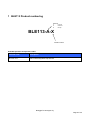
BLE113 PRELIMINARY DATA SHEET Tuesday, 07 May 2013 Version 0.55 Copyright © 2000-2013 Bluegiga Technologies All rights reserved. Bluegiga Technologies assumes no responsibility for any errors which may appear in this manual. Furthermore, Bluegiga Technologies reserves the right to alter the hardware, software, and/or specifications detailed here at any time without notice and does not make any commitment to update the information contained here. Bluegiga’s products are not authorized for use as critical components in life support devices or systems. The WRAP is a registered trademark of Bluegiga Technologies The Bluetooth trademark is owned by the Bluetooth SIG Inc., USA and is licensed to Bluegiga Technologies. All other trademarks listed herein are owned by their respective owners. Bluegiga Technologies Oy VERSION HISTORY Version Comment 0.1 Draft 0.2 Confidential watermark added 0.3 Marketing information updated 0.4 Current consumption, recommended land pattern, layout guide, example schematic, antenna characteristics 0.5 Minor changes 0.51 Absolute maximum ratings: all supply nets must have the same voltage 0.52 Pin dimensions and recommended land pattern 0.53 FCC and IC statements 0.54 TXP vs HW config setting 0.55 Dimensions Bluegiga Technologies Oy TABLE OF CONTENTS 1 BLE113 Product numbering ..........................................................................................................................6 2 Pinout and Terminal Description ...................................................................................................................7 2.1 I/O Ports .............................................................................................................................................. 10 2.2 UART ................................................................................................................................................... 10 2.3 Electrical Characteristics ..................................................................................................................... 11 2.4 Absolute Maximum Ratings ................................................................................................................ 11 2.5 Recommended Operating Conditions ................................................................................................. 11 2.6 DC Characteristics .............................................................................................................................. 11 2.7 Current Consumption .......................................................................................................................... 12 2.8 Antenna characteristics ....................................................................................................................... 13 3 Physical Dimensions .................................................................................................................................. 16 4 Power-On Reset and Brownout Detector ................................................................................................... 18 5 Design Guidelines ...................................................................................................................................... 19 5.1 General Design Guidelines ................................................................................................................. 19 5.2 Layout Guide Lines ............................................................................................................................. 19 5.3 BLE113-A Layout Guide ..................................................................................................................... 20 6 Soldering Recommendations ..................................................................................................................... 22 7 Block diagram ............................................................................................................................................. 23 8 Certifications ............................................................................................................................................... 26 9 8.1 Bluetooth ............................................................................................................................................. 26 8.2 FCC and IC ......................................................................................................................................... 26 8.3 CE ....................................................................................................................................................... 29 8.4 MIC Japan ........................................................................................................................................... 29 8.5 KCC (Korea) ........................................................................................................................................ 29 Contact Information .................................................................................................................................... 30 Bluegiga Technologies Oy BLE113 Bluetooth® Smart Module DESCRIPTION BLE113 is a Bluetooth Smart module targeted for small and low power sensors and accessories. It integrates all features required for a Bluetooth Smart application: Bluetooth radio, software stack and GATT based profiles. BLE113 Bluetooth Smart module can also host end user applications, which means no external micro controller is required in size or price constrained devices. BLE113 module has flexible hardware interfaces to connect to different peripherals and sensors. BLE113 can be powered directly from a standard 3V coin cell battery or pair of AAA batteries. KEY FEATURES: In lowest power sleep mode it consumes only 500nA and will wake up in few hundred microseconds. APPLICATIONS: Health and fitness sensors Medical sensors iPhone and iPad accessories Security and proximity tags Key fobs Smart home sensors and collectors Wireless keys HID keyboards and mice Bluetooth v. 4.0, single mode compliant o Supports master and slave modes o Up to eight connections Integrated Bluetooth Smart stack o GAP, GATT, L2CAP and SMP o Bluetooth Smart profiles Radio performance o TX power : 0 dBm to -23 dBm o Receiver sensitivity: -93 dBm Ultra low current consumption o Transmit: 18.2 mA (0dBm) o Transmit: 14.3 mA (0dBm + DC/DC) o Receive: 14.3 mA o Sleep mode 3: 0.4 uA Flexible peripheral interfaces o UART and SPI o I2C, PWM and GPIO o 12-bit ADC Host interfaces: o UART Programmable 8051 processor for standalone operation Dimensions: 9.15 x 15.75 x 2.1 mm Bluetooth, CE, FCC, IC, South Korea and Japan qualified Bluegiga Technologies Oy 1 BLE113 Product numbering Antenna: A = Internal E = External N = RF pin BLE113-A-X Firmware revision Available products and product codes Product code Description BLE113-A-v1 BLE113 with integrated chip antenna Bluegiga Technologies Oy Page 6 of 30 1 GND 2 3 4 5 6 7 8 9 10 11 12 13 14 15 16 17 18 GND GND GND GND GND GND AVDD P2_2 P2_1 P2_0 P1_7 P1_6 SCL SDA NC DVDD GND P1_5 P1_4 P1_3 P1_2 P1_1 P1_0 Pinout and Terminal Description GND NC Reset# P0_0 P0_1 P0_2 P0_3 P0_4 P0_5 P0_6 P0_7 GND 36 35 34 33 32 31 30 29 28 27 26 25 19 20 21 22 23 24 2 Figure 1: BLE113 RESET PIN NUMBER 34 PAD TYPE DESCRIPTION Active low reset. GND 1 - 7, 18, 25, 36 GND DVDD AVDD 17 8 Supply voltage Supply voltage GND Supply voltage 2V - 3.6V Supply voltage 2V - 3.6V Table 1: Supply and RF Terminal Descriptions Bluegiga Technologies Oy Page 7 of 30 PIN PIN NAME PIN TYPE NUMBER DESCRIPTION 9 P2_2 10 P2_1 11 12 13 19 20 21 22 26 27 28 29 30 31 32 33 P2_0 P1_7 P1_6 P1_5 P1_4 P1_3 P1_2 P0_7 P0_6 P0_5 P0_4 P0_3 P0_2 P0_1 P0_0 23 P1_1 24 P1_0 14 SCL I2C clock or digital I/O Can be used as I2C clock pin or digital I/O. Leave floating if not used. If grounded disable pull up. 15 SDA I2C data or digital I/O Can be used as I2C data pin or digital I/O. Leave floating if not used. If grounded disable pull up. Digital I/O Configurable I/O port, See table 3 Digital I/O Configurable I/O port with 20mA driving capability, See table 3 Table 2: Terminal Descriptions *)BLE113 is configurable as either SPI master or SPI slave Bluegiga Technologies Oy Page 8 of 30 PERIPHERAL / FUNCTION ADC USART 0 SPI (** USART 0 UART USART 1 SPI (** USART 1 UART TIMER 1 TIMER 3 TIMER 4 P0 7 6 5 4 3 2 1 0 A7 A6 A5 A4 A3 A2 A1 A0 C Alt.1 P1 7 6 4 3 2 MO MI C SS 0 2 P2 1 HARDWARE.XML Example (* 0 <usart channel="0" mode="spi_master" alternate="1" ... <usart channel="0" mode="spi_master" alternate="2" ... RT CT TX RX Alt.1 <usart channel="0" mode="uart" alternate="1" ... TX RX RT CT Alt.2 MI MO C Alt.1 <usart channel="0" mode="uart" alternate="2" ... SS <usart channel="1" mode="spi_master" alternate="1" ... MI MO C Alt.2 SS <usart channel="1" mode="spi_master" alternate="2" ... RX TX RT CT Alt.1 <usart channel="1" mode="uart" alternate="1" ... RX TX RT CT Alt.2 4 Alt.1 3 3 2 1 <usart channel="1" mode="uart" alternate="2" ... 0 <timer index="1" alternate="1" ... 4 0 1 Alt.1 Alt.2 1 SS MO MI Alt.2 Alt.2 5 1 1 2 <timer index="1" alternate="2" ... 0 <timer index="3" alternate="1" ... 0 <timer index="3" alternate="2" ... 1 Alt.1 0 <timer index="4" alternate="1" ... 0 Alt.2 DEBUG OBSSEL <timer index="4" alternate="2" ... DC DD 5 4 3 2 1 0 *) Refer to Profile Toolkit Developer Guide for detailed settings **) SS is the slave select signal when BLE113 is set as SPI slave. When set as SPI master, any available I/O can be used as chip select signal of BLE113 Table 3:Peripheral I/O Pin Mapping Bluegiga Technologies Oy Page 9 of 30 2.1 I/O Ports Each I/O port, except pins P1_0 and P1_1, can be configured as an input with either internal pull-up or pulldown, or tri-state. Pull-down or pull-up can only be configured to whole port, not individual pins. Unused I/O pins should have defined level and not be floating. See the Profile Toolkit developer guide for more information about the configuration. During reset the I/O pins are configured as inputs with pull-ups. P1_0 and P1_1 are inputs but do not have pull-up or pull-down. 2.2 UART UART baud rate can be configured up 2 Mbps. See the Profile Toolkit developer guide for more information. Following table lists commonly used baud rates for BLE113 Baud rate (bps) Error (%) 2400 0.14 4800 0.14 9600 0.14 14 400 0.03 19 200 0.14 28 800 0.03 38 400 0.14 57 600 0.03 76 800 0.14 115 200 0.03 230 400 0.03 Table 4: Commonly used baud rates for BLE113 Bluegiga Technologies Oy Page 10 of 30 2.3 Electrical Characteristics 2.4 Absolute Maximum Ratings Note: These are absolute maximum ratings beyond which the module can be permanently damaged. These are not maximum operating conditions. The maximum recommended operating conditions are in the table 6. Rating Storage Temperature Min -40 Max 85 Unit °C AVDD,DVDD (* -0.3 3.9 V VSS-0.4 VDD+0.4 V Max 85 3.6 Unit °C V Other Terminal Voltages *)All supply nets must have the same voltage Table 5: Absolute Maximum Ratings 2.5 Recommended Operating Conditions Rating Operating Temperature Range AVDD, DVDD Min -40 2.0 *) Supply voltage noise should be less than 10mVpp. Excessive noise at the supply voltage will reduce the RF performance. Table 6: Recommended Operating Conditions 2.6 DC Characteristics Parameter Logic-0 input voltage Logic-1 input voltage Logic-0 input current Logic-1 input current I/O pin pull-up and pull-down resistors Logic-0 output volatge, 4 mA pins Logic-1 output voltage, 4 mA pins Test Conditions Min Input equals 0V Input equals VDD 2.5 -50 -50 Typ Max Unit 0.5 V V nA nA kΩ V V 50 50 20 Output load 4 mA Outoput load 4 mA 0.5 2.4 For detailed I/O terminal characteristic and timings refer to the CC2541 datasheet available in (http://www.ti.com/lit/ds/symlink/cc2541.pdf) Bluegiga Technologies Oy Page 11 of 30 2.7 Current Consumption Power mode Transmit Receive Power mode 1 Power mode 2 Power mode 3 hardware.xml <txpower power = "1"/> <slow clock enable = "true"/> <txpower power = "7"/> <slow clock enable = "true"/> <txpower power = "15"/> <slow clock enable = "true"/> <txpower power = "1"/> <slow clock enable = "false"/> <txpower power = "7"/> <slow clock enable = "false"/> <txpower power = "15"/> <slow clock enable = "false"/> <slow clock enable = "true"/> <slow clock enable = "false"/> Min Typ Max Unit 18.2 mA 18.3 mA 20.7 mA 23.6 mA 23.6 mA 26.1 mA 21.9 27.0 270 1 0.5 mA mA uA uA uA Table 7: Current consumption of BLE113 Figure 2: BLE113 TX peak current as a function of the setting in the HW configuration file Bluegiga Technologies Oy Page 12 of 30 Figure 3: BLE113 TX power as a function of the setting in the HW configuration file 2.8 Antenna characteristics The antenna is monopole type of chip antenna. The antenna impedance matching is optimized for 1 mm – 2 mm mother board PCB thickness. The radiation pattern is impacted by the layout of the mother board. Typically the highest gain is towards GND plane and weakest gain away from the GND plane. Figures 4 – 6 show the radiation pattern of BLE113 when mounted to the development board. The typical efficiency of the antenna is 25…35% depending on the mother board layout. Maximum gain is 0.5 dBi. Bluegiga Technologies Oy Page 13 of 30 Figure 4: Radiation pattern of BLE113, top view Figure 5: Radiation pattern of BLE113, front view Bluegiga Technologies Oy Page 14 of 30 Figure 6: Radiation pattern of BLE113, side view Bluegiga Technologies Oy Page 15 of 30 3 Physical Dimensions Figure 7: Physical dimensions and pinout (top view) 15.73 mm (+/-0.1mm) Antenna 0.85 mm 4.9 mm 9.15 mm (+/-0.1mm) 0.3 mm 0.6 mm 5.53 mm 9.6 mm 0.6 mm Figure 8: Physical dimensions (top view) Bluegiga Technologies Oy Page 16 of 30 1.3 mm 0.6 mm 1.9 mm (+/-10%) 15.73 (+/-0.1) mm Figure 9: Physical dimensions (side view) Figure 10: Recommended land pattern for BLE113-A Bluegiga Technologies Oy Page 17 of 30 4 Power-On Reset and Brownout Detector BLE113 includes a power-on reset (POR), providing correct initialization during device power on. It also includes a brownout detector (BOD) operating on the regulated 1.8-V digital power supply only. The BOD protects the memory contents during supply voltage variations which cause the regulated 1.8-V power to drop below the minimum level required by digital logic, flash memory, and SRAM. When power is initially applied, the POR and BOD hold the device in the reset state until the supply voltage rises above the power-on-reset and brownout voltages. Bluegiga Technologies Oy Page 18 of 30 5 Design Guidelines 5.1 General Design Guidelines LE113 can be used directly with a coin cell battery. Due to relatively high internal resistance of a coin cell battery it is recommended to place a 100uF capacitor in parallel with the battery. The internal resistance of a coin cell battery is initially in the range of 10 ohms but the resistance increases rapidly as the capacity is used. Basically the higher the value of the capacitor the higher is the effective capacity of the battery and thus the longer the life time for the application. The minimum value for the capacitor depends on the end application and the maximum transmit power used. The leakage current of a 100uF capacitor is in the range of 0.5 uA to 3 uA and generally ceramic capacitors have lower leakage current than tantalum or aluminum electrolytic capacitors. Optionally TI’s TPS62730 can be used to reduce the current consumption during TX/RX and data processing 6 4 1 stages. TPS62730 is 5an ultra low power DC/DC converter with3 by-pass mode and2 will reduce the current consumption during transmission nominally by ~20% when using 3V coin cell battery. REVISION RECORD L TR ECO NO: APPROVED: DATE: 2 V...3 V3 _ M OD D D R4 2 1 VBAT P2 _ 2 /PROG P2 _ 1 /PROG P1 _ 7 /DCDC C1 4 1 0 0 u F/1 6 V/1 0 % /TAN SCL SDA GND NC RESET P0 _ 0 P0 _ 1 P0 _ 2 P0 _ 3 P0 _ 4 P0 _ 5 P0 _ 6 P0 _ 7 GND 36 35 34 33 32 31 30 29 28 27 26 25 R1 10K, 50V, 0.063W 2 1 GND GND GND GND GND GND GND AVDD P2 _ 2 P2 _ 1 P2 _ 0 P1 _ 7 P1 _ 6 SCL SDA NC DVDD GND 3 2 2 1 2 3 4 5 6 7 8 9 10 11 12 13 14 15 16 17 18 SW1 4 1 C6 2 V...3 V3 _ M OD 4 .7K, 50V, 0.063W 2 R16 R17 1 1 4 .7K, 50V, 0.063W C11 2.2uF/10 V/ X5R C10 2.2uF/10V/ X5R P1 _ 7 /DCDC 0.4 7uF/6.3V/ X5R C5 L1 2 .2 µ H± 2 0 % , 1 3 0 m A, 0 .4 3 o h m 0.4 7uF/6.3V/ X5R NP 19 P1_ 5 20 P1_ 4 21 P1_ 3 22 P1_ 2 23 P1_ 1 24 P1_ 0 2 V...3 V3 _ M OD M OD2 C C 3 SCL 4 GND NC INT1 SCL GND GND INT2 7 2 V...3 V3 _ SW J1 P2 _ 2 /PROG 12 11 1 2 3 4 5 6 P2 _ 1 /PROG 78 RESET_ N 10 91 0 9 HEADER_ 2 X5 _ SM D_ 1 .2 7 M M PROGRAMMING INTERFACE U2 M M A8 4 5 1 Q SDA 6 13 4.7uF/4V/ X5R/ 10% C7 14 VDD 15 NC NC BYP SDA 5 VDDIO NC 2 8 1 SA0 0.1 uF/10V/ X5R C8 NC 16 BL E1 1 X_ P2 B B Figure 11: Example schematic for BLE113 with a coin cell battery, TPS62730 DCDC converter and an I2C accelerometer 5.2 Layout Guide Lines Use good layout practices to avoid excessive noise coupling to supply voltage traces or sensitive analog Blueg ig a Technolog ies Oy signal traces. If using overlapping ground planes use stitching vias separated by max 3 mm to avoid emission BLE113 Example Schematic from the edges of the PCB. Connect all the GND pins directly to a solid GND plane and make sure that there is a low impedance path for the return current following the signal and supply traces all the way from start to C the end. COM PANY: A A TITL E: DRAWN: DATED: PR A CHECKED: 2012-08-03 DATED: - CODE: - QUAL ITY CONTROL : DATED: REL EASED: DATED: SCAL E: SIZE: DRAWING NO: SHEET: 1OF 5 A good practice is to dedicate one of the inner layers to a solid GND plane and one of the inner layers to supply voltage planes and traces and route all the signals on top and bottom layers of the PCB. This arrangement will make sure that any return current follows the forward current as close as possible and any loops are minimized. Bluegiga Technologies Oy Page 19 of 30 REV: 1.0 not separate GND regions but keep one solid GND plane. – Keep the trace as short as possible Recommended PCB layer configuration Signals GND Power Signals Figure 12: Typical 4-layer PCB construction Overlapping GND layers without GND stitching vias Overlapping GND layers with GND stitching vias shielding the RF energy Figure 13: Use of stitching vias to avoid emissions from the edges of the PCB 5.3 BLE113-A Layout Guide For optimal performance of the antenna place the module at the corner of the PCB as shown in the figure 14. Do not place any metal (traces, components, battery etc.) within the clearance area of the antenna. Connect all the GND pins directly to a solid GND plane. Place the GND vias as close to the GND pins as possible. Use good layout practices to avoid any excessive noise coupling to signal lines or supply voltage lines. Avoid placing plastic or any other dielectric material closer than 5 mm from the antenna. Any dielectric closer than 5 mm from the antenna will detune the antenna to lower frequencies. Figure 14: Recommended layout for BLE113-A Bluegiga Technologies Oy Page 20 of 30 Figure 15: Typical return loss of BLE113-A with two different mother board PCB thickness Bluegiga Technologies Oy Page 21 of 30 6 Soldering Recommendations BLE113 is compatible with industrial standard reflow profile for Pb-free solders. The reflow profile used is dependent on the thermal mass of the entire populated PCB, heat transfer efficiency of the oven and particular type of solder paste used. Consult the datasheet of particular solder paste for profile configurations. Bluegiga Technologies will give following recommendations for soldering the module to ensure reliable solder joint and operation of the module after soldering. Since the profile used is process and layout dependent, the optimum profile should be studied case by case. Thus following recommendation should be taken as a starting point guide. - Refer to technical documentations of particular solder paste for profile configurations - Avoid using more than one flow. - Reliability of the solder joint and self-alignment of the component are dependent on the solder volume. Minimum of 150m stencil thickness is recommended. - Aperture size of the stencil should be 1:1 with the pad size. - A low residue, “no clean” solder paste should be used due to low mounted height of the component. Figure 16: Reference reflow profile Bluegiga Technologies Oy Page 22 of 30 7 Block diagram BLE113 is based on TI’s CC2541 chip. Embedded 32 MHz and 32.678 kHz crystals are used for clock generation. Matched balun and low pass filter provide optimal radio performance with extremely low spurious emissions. Small ceramic chip antenna gives good radiation efficiency even when the module is used in layouts with very limited space. 32 MHz XTAL 32.768 kHz XTAL Clock 2V – 3.6V Reset Voltage regulator CC2540 Reset Debug interface Power-on reset SRAM 8051 CPU core and memory arbitrator Flash Analog comparator DMA I/O controller I/O IRQ controller Radio arbiter Radio registers Link layer engine SRAM ADC Demodulator Synth Modulator Assembly variant: BLE112-A or BLE112-E I2C USART 0 USART 1 TIMER 1 Receive Frequency synthetisizer U.Fl connector (BLE112-E) Transmit TIMER 2 TIMER 3 Balun + LPF TIMER 4 Chip antenna BLE112-A) Figure 17: Simplified block diagram of BLE113 CPU and Memory The 8051 CPU core is a single-cycle 8051-compatible core. It has three different memory access buses (SFR, DATA, and CODE/XDATA), a debug interface, and an 18-input extended interrupt unit. The memory arbiter is at the heart of the system, as it connects the CPU and DMA controller with the physical memories and all peripherals through the SFR bus. The memory arbiter has four memory-access points, access of which can map to one of three physical memories: an SRAM, flash memory, and XREG/SFR registers. It is responsible for performing arbitration and sequencing between simultaneous memory accesses to the same physical memory. The SFR bus is a common bus that connects all hardware peripherals to the memory arbiter. The SFR bus also provides access to the radio registers in the radio register bank, even though these are indeed mapped into XDATA memory space. Bluegiga Technologies Oy Page 23 of 30 The 8-KB SRAM maps to the DATA memory space and to parts of the XDATA memory spaces. The SRAM is an ultralow-power SRAM that retains its contents even when the digital part is powered off (power modes 2 and 3). The 128/256 KB flash block provides in-circuit programmable non-volatile program memory for the device, and maps into the CODE and XDATA memory spaces. Peripherals Writing to the flash block is performed through a flash controller that allows page-wise erasure and 4-bytewise programming. A versatile five-channel DMA controller is available in the system, accesses memory using the XDATA memory space, and thus has access to all physical memories. Each channel (trigger, priority, transfer mode, addressing mode, source and destination pointers, and transfer count) is configured with DMA descriptors that can be located anywhere in memory. Many of the hardware peripherals (AES core, flash controller, USARTs, timers, ADC interface, etc.) can be used with the DMA controller for efficient operation by performing data transfers between a single SFR or XREG address and flash/SRAM. Each CC2541 contains a unique 48-bit IEEE address that can be used as the public device address for a Bluetooth device. Designers are free to use this address, or provide their own, as described in the Bluetooth specification. The interrupt controller services a total of 18 interrupt sources, divided into six interrupt groups, each of which is associated with one of four interrupt priorities. I/O and sleep timer interrupt requests are serviced even if the device is in a sleep mode (power modes 1 and 2) by bringing the CC2541 back to the active mode. The debug interface implements a proprietary two-wire serial interface that is used for in-circuit debugging. Through this debug interface, it is possible to erase or program the entire flash memory, control which oscillators are enabled, stop and start execution of the user program, execute instructions on the 8051 core, set code breakpoints, and single-step through instructions in the code. Using these techniques, it is possible to perform in-circuit debugging and external flash programming elegantly. The I/O controller is responsible for all general-purpose I/O pins. The CPU can configure whether peripheral modules control certain pins or whether they are under software control, and if so, whether each pin is configured as an input or output and if a pullup or pulldown resistor in the pad is connected. Each peripheral that connects to the I/O pins can choose between two different I/O pin locations to ensure flexibility in various applications. The sleep timer is an ultra low power timer that uses an external 32.768-kHz crystal oscillator. The sleep timer runs continuously in all operating modes except power mode 3. Typical applications of this timer are as a realtime counter or as a wake-up timer to exit power modes 1 or 2. Timer 1 is a 16-bit timer with timer/counter/PWM functionality. It has a programmable prescaler, a 16-bit period value, and five individually programmable counter/capture channels, each with a 16-bit compare value. Each of the counter/capture channels can be used as a PWM output or to capture the timing of edges on input signals. It can also be configured in IR generation mode, where it counts timer 3 periods and the output is ANDed with the output of timer 3 to generate modulated consumer IR signals with minimal CPU interaction. Timer 2 is a 40-bit timer used by the Bluetooth low energy stack. It has a 16-bit counter with a configurable timer period and a 24-bit overflow counter that can be used to keep track of the number of periods that have transpired. A 40-bit capture register is also used to record the exact time at which a start-of-frame delimiter is received/transmitted or the exact time at which transmission ends. There are two 16-bit timer-compare registers and two 24-bit overflow-compare registers that can be used to give exact timing for start of RX or TX to the radio or general interrupts. Timer 3 and timer 4 are 8-bit timers with timer/counter/PWM functionality. They have a programmable prescaler, an 8-bit period value, and one programmable counter channel with an 8-bit compare value. Each of the counter channels can be used as PWM output. USART 0 and USART 1 are each configurable as either an SPI master/slave or a UART. They provide double buffering on both RX and TX and hardware flow control and are thus well suited to high-throughput full-duplex applications. Each USART has its own high-precision baud-rate generator, thus leaving the ordinary timers Bluegiga Technologies Oy Page 24 of 30 free for other uses. When configured as SPI slaves, the USARTs sample the input signal using SCK directly instead of using some oversampling scheme, and are thus well-suited for high data rates. The AES encryption/decryption core allows the user to encrypt and decrypt data using the AES algorithm with 128-bit keys. The AES core also supports ECB, CBC, CFB, OFB, CTR, and CBC-MAC, as well as hardware support for CCM. The ADC supports 7 to 12 bits of resolution with a corresponding range of bandwidths from 30-kHz to 4-kHz, respectively. DC and audio conversions with up to eight input channels (I/O controller pins) are possible. The inputs can be selected as single-ended or differential. The reference voltage can be internal, AVDD, or a single-ended or differential external signal. The ADC also has a temperature-sensor input channel. The ADC can automate the process of periodic sampling or conversion over a sequence of channels. 2 The I C module provides a digital peripheral connection with two pins and supports both master and slave 2 operation. I C support is compliant with the NXP I2C specification version 2.1 and supports standard mode (up to 100 kbps) and fast mode (up to 400 kbps). In addition, 7-bit device addressing modes are supported, as well as master and slave modes.. The ultralow-power analog comparator enables applications to wake up from PM2 or PM3 based on an analog signal. Both inputs are brought out to pins; the reference voltage must be provided externally. The comparator output is connected to the I/O controller interrupt detector and can be treated by the MCU as a regular I/O pin interrupt. RF front end RF front end includes combined matched balun and low pass filter, and ceramic chip antenna with matching network. Optimal matching combined with effective low pass filter provides extremely low in-band spurious emissions and harmonics. Bluegiga Technologies Oy Page 25 of 30 8 Certifications BLE113 is compliant to the following specifications. 8.1 Bluetooth TBA 8.2 FCC and IC This device complies with Part 15 of the FCC Rules. Operation is subject to the following two conditions: (1) this device may not cause harmful interference, and (2) this device must accept any interference received, including interference that may cause undesired operation. Any changes or modifications not expressly approved by Bluegiga Technologies could void the user’s authority to operate the equipment. FCC RF Radiation Exposure Statement: This equipment complies with FCC radiation exposure limits set forth for an uncontrolled environment. End users must follow the specific operating instructions for satisfying RF exposure compliance. This transmitter meets both portable and mobile limits as demonstrated in the RF Exposure Analysis and should not be used closer than 5 mm from a human body in portable configuration. This transmitter must not be co-located or operating in conjunction with any other antenna or transmitter except in accordance with FCC multi-transmitter product procedures. IC Statements: This device complies with Industry Canada licence-exempt RSS standard(s). Operation is subject to the following two conditions: (1) this device may not cause interference, and (2) this device must accept any interference, including interference that may cause undesired operation of the device. Under Industry Canada regulations, this radio transmitter may only operate using an antenna of a type and maximum (or lesser) gain approved for the transmitter by Industry Canada. To reduce potential radio interference to other users, the antenna type and its gain should be so chosen that the equivalent isotropically radiated power (e.i.r.p.) is not more than that necessary for successful communication. OEM Responsibilities to comply with FCC and Industry Canada Regulations The BLE113 module has been certified for integration into products only by OEM integrators under the following condition: The antenna(s) must be installed such that a minimum separation distance of 5 mm is maintained between the radiator (antenna) and all persons at all times. The transmitter module must not be co-located or operating in conjunction with any other antenna or transmitter except in accordance with FCC multi-transmitter product procedures. Bluegiga Technologies Oy Page 26 of 30 As long as the two condition above is met, further transmitter testing will not be required. However, the OEM integrator is still responsible for testing their end-product for any additional compliance requirements required with this module installed (for example, digital device emissions, PC peripheral requirements, etc.). IMPORTANT NOTE: In the event that these conditions can not be met (for certain configurations or colocation with another transmitter), then the FCC and Industry Canada authorizations are no longer considered valid and the FCC ID and IC Certification Number can not be used on the final product. In these circumstances, the OEM integrator will be responsible for re-evaluating the end product (including the transmitter) and obtaining a separate FCC and Industry Canada authorization. End Product Labeling The BLE113 module is labeled with its own FCC ID and IC Certification Number. If the FCC ID and IC Certification Number are not visible when the module is installed inside another device, then the outside of the device into which the module is installed must also display a label referring to the enclosed module. In that case, the final end product must be labeled in a visible area with the following: “Contains Transmitter Module FCC ID: QOQBLE113” “Contains Transmitter Module IC: 5123A-BGTBLE113” or “Contains FCC ID: QOQBT113” “Contains IC: 5123A-BGTBLE113” The OEM integrator has to be aware not to provide information to the end user regarding how to install or remove this RF module or change RF related parameters in the user manual of the end product. 8.2.1 FCC et IC Déclaration d’IC : Ce dispositif est conforme aux normes RSS exemptes de licence d’Industrie Canada. Son fonctionnement est assujetti aux deux conditions suivantes : (1) ce dispositif ne doit pas provoquer de perturbation et (2) ce dispositif doit accepter toute perturbation, y compris les perturbations qui peuvent entraîner un fonctionnement non désiré du dispositif. Selon les réglementations d’Industrie Canada, cet émetteur radio ne doit fonctionner qu’avec une antenne d’une typologie spécifique et d’un gain maximum (ou inférieur) approuvé pour l’émetteur par Industrie Canada. Pour réduire les éventuelles perturbations radioélectriques nuisibles à d’autres utilisateurs, le type d’antenne et son gain doivent être choisis de manière à ce que la puissance isotrope rayonnée équivalente (P.I.R.E.) n’excède pas les valeurs nécessaires pour obtenir une communication convenable. Responsabilités des OEM quant à la conformité avec les réglementations de FCC et d’Industrie Canada Les modules BLE113 ont été certifiés pour entrer dans la fabrication de produits exclusivement réalisés par des intégrateurs dans les conditions suivantes : Bluegiga Technologies Oy Page 27 of 30 L’antenne (ou les antennes) doit être installée de façon à maintenir à tout instant une distance minimum de 5 mm entre la source de radiation (l’antenne) et toute personne physique. Le module transmetteur ne doit pas être installé ou utilisé en concomitance avec une autre antenne ou un autre transmetteur. Tant que ces deux conditions sont réunies, il n’est pas nécessaire de procéder à des tests supplémentaires sur le transmetteur. Cependant, l’intégrateur est responsable des tests effectués sur le produit final afin de se mettre en conformité avec d’éventuelles exigences complémentaires lorsque le module est installé (exemple : émissions provenant d’appareils numériques, exigences vis-à-vis de périphériques informatiques, etc.) REMARQUE IMPORTANTE : En cas d’inobservance de ces conditions (en ce qui concerne certaines configurations ou l’emplacement du dispositif à proximité d’un autre émetteur), les autorisations de FCC et d’Industrie Canada ne seront plus considérées valables et l’identification de FCC et le numéro de certification d’IC ne pourront pas être utilisés sur le produit final. Dans ces cas, l’intégrateur OEM sera chargé d’évaluer à nouveau le produit final (y compris l’émetteur) et d’obtenir une autorisation indépendante de FCC et d’Industrie Canada. Étiquetage du produit final Le module BLE113 est étiqueté avec sa propre identification FCC et son propre numéro de certification IC. Si l’identification FCC et le numéro de certification IC ne sont pas visibles lorsque le module est installé à l’intérieur d’un autre dispositif, la partie externe du dispositif dans lequel le module est installé devra également présenter une étiquette faisant référence au module inclus. Dans ce cas, le produit final devra être étiqueté sur une zone visible avec les informations suivantes : « Contient module émetteur identification FCC : QOQBLE113 » « Contient module émetteur IC : 5123A-BGTBLE113 » ou « Contient identification FCC : QOQBLE113 » « Contient IC : 5123A-BGTBLE113 » Dans le guide d’utilisation du produit final, l’intégrateur OEM doit s’abstenir de fournir des informations à l’utilisateur final portant sur les procédures à suivre pour installer ou retirer ce module RF ou pour changer les paramètres RF. Bluegiga Technologies Oy Page 28 of 30 8.3 CE TBA 8.4 MIC Japan TBA 8.5 KCC (Korea) Bluegiga Technologies Oy Page 29 of 30 9 Contact Information Sales: [email protected] Technical support: [email protected] http://techforum.bluegiga.com Orders: [email protected] WWW: www.bluegiga.com www.bluegiga.hk Head Office / Finland: Phone: +358-9-4355 060 Fax: +358-9-4355 0660 Sinikalliontie 5A 02630 ESPOO FINLAND Postal address / Finland: P.O. BOX 120 02631 ESPOO FINLAND Sales Office / USA: Phone: +1 770 291 2181 Fax: +1 770 291 2183 Bluegiga Technologies, Inc. 3235 Satellite Boulevard, Building 400, Suite 300 Duluth, GA, 30096, USA Sales Office / Hong-Kong: Phone: +852 3972 2186 Bluegiga Technologies Ltd. Unit 10-18 32/F, Tower 1, Millennium City 1 388 Kwun Tong Road Kwun Tong, Kowloon Hong Kong Bluegiga Technologies Oy Page 30 of 30