1
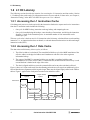
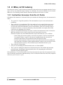
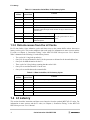
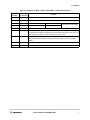
Order Number: AN2180/D
Rev. 0, 8/2001
Semiconductor Products Sector
Application Note
Cache Latencies of the MPC7450
Bill Brock and Michael Everman
The MPC7450 microprocessor contains separate 32-Kbyte, eight-way set-associative level 1 (L1)
instruction and data caches to allow the execution units and registers rapid access to instructions and data.
In addition, the MPC7450 microprocessor features an integrated 256-Kbyte level 2 (L2) cache and the
address tags and status bits for a level 3 (L3) cache that supports either 1 or 2 Mbytes of external cache
memory.
This document describes the instruction and data access latencies of the L1, L2, and L3 caches of the
MPC7450. Instruction fetch latency depends on the instruction memory management unit (MMU), the
type of execution unit and instruction, the fetch hits in the BTIC, and the L1 instruction cache, the on-chip
L2 cache, and the off-chip L3 cache, if implemented. Data access latency depends on the data MMU, the
L1 data cache, the on-chip L2 cache, and the off-chip L3 cache, if implemented. This application note
assumes an MMU hit, explains the formulas for calculating instruction and data latencies, and gives typical
examples.
1.1 Terminology
In this document, the term ‘cache’ applies to either the instruction or data cache unless otherwise specified.
Other terms and their definitions used in this document are as follows:
•
•
Latency: The number of clock cycles necessary to execute an instruction and make ready the
results of that execution for a subsequent instruction.
Core arbitration: The arbitration performed by the processor to gain access to the internal address
bus
This document contains information on a new product under development by Motorola.
Motorola reserves the right to change or discontinue this product without notice.
© Motorola, Inc., 2001. All rights reserved.
L1 Hit Latency
1.2 L1 Hit Latency
The following sections describe the latencies for accessing the L1 instruction and data caches. Section
1.2.2 addresses data cache reads. For information on store accesses and the L1 data cache, see Chapter 6,
“Instruction Timing,” in the MPC7450 RISC Microprocessor User’s Manual.
1.2.1 Accessing the L1 Instruction Cache
Calculating total processor clocks required for the instruction fetch unit to request and receive instructions
from the L1 instruction cache includes the following:
•
•
One cycle for MMU lookup, instruction cache tag lookup, and comparing the two
One cycle for multiplexing the lookups, some decoding of instructions, and driving the instruction
from the L1 cache to the instruction queue. A maximum number of four instructions can be
fetched per cycle.
This two-cycle value is the best case for L1 instruction cache hit latency, calculated from a non-branching
instruction, i.e., an instruction that does not branch, or a branch instruction that misses in the branch target
instruction cache (BTIC).
1.2.2 Accessing the L1 Data Cache
The data cache read hit latency is three cycles, as follows:
1. The effective address is calculated. The second half of this first cycle is the MMU translation of the
effective address to the physical address and simultaneous with this is the cache tag/status
information lookup.
2. The output of the MMU is compared with the tags, and this is combined with the status
information to see if a hit occurs. If there is a data cache hit, the data from the selected way is read
out and the data is latched at the edge of the cache.
3. The data is aligned and driven out to the rename buffers and to any other unit that is affected.
Figure 1 shows an L1 data cache read. Note that floating-point unit accesses require an additional cycle to
forward data because alignment and driving take longer. Data must be aligned right justified to the LSB on
the bus. Figure 1 applies to the fixed-point execution units and Altivec units.
3-Cycle Access
Cycle 0
Cycle 1
Cycle 2
Core Clock
EA1
MMU Translate1
Cache Tag Lookup Way Select
Align
Drive to
rename
buffer
Figure 1. L1 Data Cache Access
2
Cache Latencies of the MPC7450
L1 Miss, L2 Hit Latency
1.3 L1 Miss, L2 Hit Latency
If no hit occurs in the L1 cache for either an instruction or data read, the access propagates into the L1 miss
queue and L1 core arbitration begins. During core arbitration, the processor arbitrates for the internal
address bus. The following sections describe instruction and data accesses in the L2 cache.
1.3.1 Instruction Accesses from the L2 Cache
Calculation of the instruction L1 miss and L2 hit cycles includes the following factors, also summarized in
Table 1:
•
•
•
•
•
•
Two cycles for L1 tag look up and miss. The actual number of cycles is one and a half, but is
rounded up.
Three cycles for L1 core arbitration. This is the number of cycles required for the processor to
arbitrate for the internal address bus after a miss. Note that L1 core arbitration for instruction
accesses may require more than three cycles in some instances. If the core is already trying to
broadcast a load, store, or castout to the memory subsystem (MSS), for example, these events
could cause core arbitration to be delayed.
One cycle for the MSS arbitration to access the L2 cache. If an instruction is in the L2 cache, the
MSS must arbitrate access to the L2 cache before the cache transfer can occur.
Note that exceptions may cause MSS arbitration to require more than one cycle, as follows:
– If the existing accesses have priority over the one in question, L2 access can be delayed.
For example, if there is a prior L2 miss that is reloading from the bus, this will win
arbitration and block the current arbitration from the instruction cache.
– In an L2 castout operation, if there was a prior access that caused a line to be deallocated,
and if that data is valid and in a block marked modified, it must be cast out of the L2 cache
and written back to memory. That writeback requires arbitration and more cycles.
Three cycles for L2 tag lookup
One cycle for forwarding the instruction back to the core from the MSS
Three cycles for sending the instruction to the instruction queue. This includes the instruction
predecode stage, forwarding the instruction back to the core, and putting the valid fetched
instruction into the instruction queue.
Full fetch latency is 13 cycles from fetch to arrival into the instruction queue (IQ) for an instruction cache
miss/L2 cache hit. Note that the additional latency for an L1 instruction cache miss and L2 hit (compared
to the two-cycle L1 hit) is 11 cycles.
Cache Latencies of the MPC7450
3
L3 Latency
Table 1. L1 Instruction Cache Miss, L2 Hit Latency Cycles
Cycle
Number
Total Cycles
per Function
1, 2
2
Instruction cache latency: L1 tag lookup and miss
3, 4, 5
3
L1 core arbitration
6
1
L2 MSS arbitration
7, 8, 9
3
L2 tag lookup and hit
10
1
L2 MSS forwarding instruction back to core.
Note that cycles 6 through 10 are common to any L2 cache access
from the core.
11
1
Instruction pre-decode stage
12
1
Instruction forwarding
13
1
Placing valid instruction in the
instruction queue
Function
Reloading instruction into the L1
cache
1.3.2 Data Accesses from the L2 Cache
For L2 data fetches, fewer arbitration cycles and faster access to the rename buffers reduce data access
latency to nine cycles. This section addresses data cache reads; for information on store accesses and the
L2 cache, see Chapter 6, “Instruction Timing,” in the MPC7450 RISC Microprocessor User’s Manual.
Table 2 summarizes the following L2 cache latency factors:
•
•
•
•
•
•
Two cycles for L1 tag look up and miss
One cycle for core arbitration in the L1 for the processor to arbitrate for the internal address bus.
One cycle for MSS arbitration for the L2
Three cycles for L2 tag lookup, assuming that the cache is idle
One cycle to send data from the L2 to the core
One cycle to send the data to the rename buffer
Table 2. L1 Data Cache Miss, L2 Hit Latency Cycles
Cycle
Number
Total Cycles
per Function
1, 2
2
Data cache latency: L1 tag lookup and miss
3
1
L1 core arbitration
4
1
L2 MSS arbitration
5, 6, 7
3
L2 tag lookup and hit
8
1
L2 send data to core
9
1
Place data in rename buffer
Function
1.4 L3 Latency
This section describes instruction and data access latencies from the optional MPC7450 L3 cache. For
information on store accesses and the L3 cache, see Chapter 6, “Instruction Timing,” in the MPC7450
RISC Microprocessor User’s Manual.
4
Cache Latencies of the MPC7450
L3 Latency
1.4.1 Instruction Accesses from the L3 Cache
If a miss occurs in the L1 cache, the MPC7450 checks for a hit in the L2 and L3 simultaneously. If there is
no hit in the L2 cache, the total number of cycles for the L3 fetch are calculated as follows:
•
•
•
•
•
Two cycles for L1 tag look up and miss
Three cycles for core arbitration in the L1, for the processor to arbitrate for the internal address
bus.
One cycle for L3 MSS arbitration, when the MSS arbitrates access to the L3 cache. Note that
simultaneously with this L3 process, the MPC7450 initiates the L2 MSS arbitration process.
Four cycles for L3 tag lookup and hit, assuming that the cache is idle. This L3 lookup operates in
parallel with the L2 lookup, but the results from the L3 lookup are only used or applied when there
is no hit in the L2. Note that the L3 tag lookup and hit requires one cycle more than the L2 tag
lookup and hit.
Zero to three cycles for L3 clock alignment, assuming a 4:1 L3 clock divider ratio. If the read
request arrives at the L3 interface on a processor clock edge that is not aligned with the L3 clock,
the request must wait until the next rising L3 clock edge for the address to be launched on the L3
interface. Figure 2 shows the clock alignment requirements.
Note that if a read request arrives at the L3 interface on a processor clock edge that is aligned with
the L3 clock, no cycles are required for L3 clock alignment and no wait occurs for the address to
be sent.
Note: If a request arrives on the second processor clock edge, it must wait three more
clock cycles for alignment with the L3 clock.
Internal
0
Processor
CLK
1
2
3
0
1
2
3
0
1
2
3
0
1
2
3
0
1
2
3
0
1
2
L3_CLKn
Figure 2. L3 Clock Alignment for a 4:1 Ratio
•
•
•
Twenty-three cycles for SRAM access time. This computation assumes a 4:1 clock divider ratio
and depends on other factors such as SRAM latency, board delays, the type of execution unit and
instruction involved, and sample point settings. Refer to “Instruction Cache Miss/L3 Cache Hit” in
Chapter 6, “Instruction Timing,” in the MPC7450 RISC Microprocessor User’s Manual.
One cycle to forward the instruction back to the core from the MSS
Three cycles to send the instruction to the instruction queue. This includes the instruction
predecode stage, forwarding the instruction back to the core, and putting the valid fetched
instruction into the instruction queue.
Cache Latencies of the MPC7450
5
L3 Latency
Table 3. L1 Instruction Cache Miss, L2 Instruction Cache Miss, L3 Hit Latency Cycles
Cycle
Number
Total Cycles
per Function
1, 2
2
Instruction cache latency: L1 tag lookup and miss
3, 4, 5
3
L1 core arbitration
6
1
L3 MSS arbitration
L2 MSS arbitration
7, 8, 9
3
L3 tag lookup
L2 tag lookup and miss
10
1
L3 hit
10–13
0-3
11–36
23 (or n)
34–37
1
L3 MSS forwarding instruction back to core
35–38
1
Instruction predecode stage
36–39
1
Instruction forwarding
37–40
1
Placing valid instruction in
the instruction queue
Function
NOTE: L2 and L3 arbitration
and lookup occur in parallel
L3 clock alignment. The clock divider ratio determines how many alignment cycles may
be required for a request to be aligned to the L3 interface. See Figure 2. It is only in 4:1
L3 mode that the number of cycles per function is 0 to 3 cycles.
The number of SRAM cycles. The number of cycles for SRAM latency given in the
MPC7450 RISC Microprocessor User’s Manual is 23 cycles, but in example, it is
variable.
Reloading instruction into the L1 cache
1.4.2 Data Accesses from the L3 Cache
The cycles required for an L3 data fetch are as follows:
•
•
•
•
•
•
•
•
6
Two cycles for L1 tag look up and miss
Three cycles for core arbitration in the L1, for the processor to arbitrate for the internal address bus
One cycle for L3 MSS arbitration when the MSS arbitrates to get into the L3 cache. Note that
simultaneously with this L3 process, the MPC7450 initiates the L2 MSS arbitration process.
Four cycles for L3 tag lookup and hit, assuming that the cache is idle. This L3 process runs in
parallel with the L2 lookup, but the results from this L3 process are only used or applied when
there is no hit in the L2. Note that the L3 tag lookup and hit requires one cycle more than the L2
tag lookup and hit.
Zero to three cycles for L3 clock alignment, assuming a 4:1 L3 clock divider ratio. If the read
request arrives at the L3 interface on a processor clock edge that is not aligned with the L3 clock,
then the request must wait until the next rising L3 clock edge for the address to be launched on the
L3 interface. See Figure 2.
Yet, if the read request arrives at the L3 interface on a processor clock edge that is aligned with the
L3 clock, no cycles are required for L3 clock alignment and no wait occurs for the address to be
sent.
Twenty-three cycles for SRAM read or load. This computation assumes a 4:1 clock divider ratio
and depends on other factors such as SRAM latency, board delays, and sample point settings.
Refer to “Instruction Cache Miss/L3 Cache Hit” in Chapter 6, “Instruction Timing,” in the
MPC7450 RISC Microprocessor User’s Manual.
One cycle for the L3 MSS forwarding data back to the core
One cycle to place the data in the rename buffer
Cache Latencies of the MPC7450
L3 Latency
Table 4. L1 Data Cache Miss, L2 Data Cache Miss, L3 Hit Latency Cycles
Cycle
Number
Total Cycles
per Function
1, 2
2
Instruction cache latency: L1 tag lookup and miss
3, 4, 5
3
L1 core arbitration
6
1
L3 MSS arbitration
L2 MSS arbitration
7, 8, 9
3
L3 tag lookup
L2 tag lookup and miss
10
1
L3 hit
10–13
0-3
11–36
23 (or n)
34–37
1
L3 MSS forwarding data back to core.
35–38
1
Place the data in the rename buffer
Function
NOTE: L2 and L3 arbitration
and lookup occur in parallel
L3 clock alignment. The clock divider ratio determines how many alignment cycles may
be required for a request to be aligned to the L3 interface. See Figure 2. It is only in 4:1
L3 mode that the number of cycles per function is 0 to 3 cycles.
The number of SRAM cycles. The number of cycles for SRAM latency given in the
MPC7450 RISC Microprocessor User’s Manual is 23 cycles, but this is a variable
number.
Cache Latencies of the MPC7450
7
DigitalDNA is a trademark of Motorola, Inc.
The PowerPC name, the PowerPC logotype, and PowerPC 603e are trademarks of International Business Machines Corporation used by Motorola
under license from International Business Machines Corporation.
Information in this document is provided solely to enable system and software implementers to use PowerPC microprocessors. There are no express
or implied copyright licenses granted hereunder to design or fabricate PowerPC integrated circuits or integrated circuits based on the information in
this document.
Motorola reserves the right to make changes without further notice to any products herein. Motorola makes no warranty, representation or guarantee
regarding the suitability of its products for any particular purpose, nor does Motorola assume any liability arising out of the application or use of any
product or circuit, and specifically disclaims any and all liability, including without limitation consequential or incidental damages. “Typical” parameters
which may be provided in Motorola data sheets and/or specifications can and do vary in different applications and actual performance may vary over
time. All operating parameters, including “Typicals” must be validated for each customer application by customer’s technical experts. Motorola does
not convey any license under its patent rights nor the rights of others. Motorola products are not designed, intended, or authorized for use as
components in systems intended for surgical implant into the body, or other applications intended to support or sustain life, or for any other application
in which the failure of the Motorola product could create a situation where personal injury or death may occur. Should Buyer purchase or use Motorola
products for any such unintended or unauthorized application, Buyer shall indemnify and hold Motorola and its officers, employees, subsidiaries,
affiliates, and distributors harmless against all claims, costs, damages, and expenses, and reasonable attorney fees arising out of, directly or indirectly,
any claim of personal injury or death associated with such unintended or unauthorized use, even if such claim alleges that Motorola was negligent
regarding the design or manufacture of the part. Motorola and
are registered trademarks of Motorola, Inc. Motorola, Inc. is an Equal
Opportunity/Affirmative Action Employer.
HOW TO REACH US:
USA/EUROPE/LOCATIONS NOT LISTED: Motorola Literature Distribution; P.O. Box 5405, Denver, Colorado 80217. 1-303-675-2140 or
1-800-441-2447
JAPAN: Motorola Japan Ltd.; SPS, Technical Information Center, 3-20-1, Minami-Azabu. Minato-ku, Tokyo 106-8573 Japan. 81-3-3440-3569
ASIA/PACIFIC: Motorola Semiconductors H.K. Ltd.; Silicon Harbour Centre, 2 Dai King Street, Tai Po Industrial Estate, Tai Po, N.T., Hong Kong.
852-26668334
TECHNICAL INFORMATION CENTER: 1-800-521-6274
HOME PAGE: http://www.motorola.com/semiconductors
DOCUMENT COMMENTS: FAX (512) 933-2625, Attn: RISC Applications Engineering
WORLD WIDE WEB ADDRESSES:
http://www.motorola.com/PowerPC
http://www.motorola.com/NetComm
http://www.motorola.com/ColdFire
AN2180/D