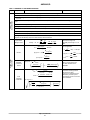
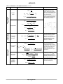
1
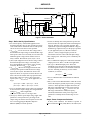
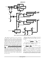
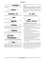
AND9062/D 5 Key Steps To Design A Compact, High‐Efficiency PFC Stage Using the NCP1611 http://onsemi.com APPLICATION NOTE This paper describes the key steps to rapidly design a Discontinuous Conduction Mode PFC stage driven by the NCP1611. The process is illustrated in a practical 160-W, universal mains application: Maximum Output Power: 160 W Rms Line Voltage Range: from 90 V to 265 V Regulation Output Voltage: 390 V Frequency Fold-back when the Line Current is less than 450 mA Introduction Fast Line/Load Transient Compensation (Dynamic Housed in a SO−8 package, the NCP1611 is designed to optimize the efficiency of your PFC stage throughout the load range. Incorporating protection features for rugged operation, it is ideal in systems where cost-effectiveness, reliability, low stand-by power and high efficiency are key requirements: Current Controlled Frequency Fold-back (CCFF): The circuit operates in Critical conduction Mode (CrM) when the instantaneous line current is medium or high. When this current is lower than a preset level, the frequency linearly decays to about 20 kHz. CCFF maximizes the efficiency at both nominal and light loads (Note 1). In particular, stand-by losses are minimized. Skip Mode: To further optimize the efficiency, the circuit skips cycles near the line zero crossing where the power transfer is particularly inefficient. If superior power factor is needed, this feature can be inhibited by forcing a minimum 0.75-V voltage. Low Start-up Current and large VCC range: The extra low start-up consumption of the B version (NCP1611B) allows the use of high-impedance resistors for charging the VCC capacitor. The A version (NCP1611A) is targeted in applications where the circuit is fed by an auxiliary power source. Its start-up level is lower than 11.25 V to allow the circuit to be powering from a 12-V rail. Both versions feature a large VCC operating range (9.5 V to 35 V). Response Enhancer and Soft OVP): Due to the slow loop response of traditional PFC stages, abrupt changes in the load or in the input voltage may cause significant over or under-shoots. This circuit drastically limits these possible deviations from the regulation point. Safety Protections: NCP1611 features make the PFC stage extremely robust. Among them, we can mention the Brown-Out Detection block (Note 2) that stops operation when the ac line is too low and the 2-level Current Sensing, that forces a low duty-ratio operation mode in the event that the current exceeds 150% of the current limit which may be caused by the inductor saturation or by a short of the bypass or boost diode. Eased Manufacturing and Safety Testing: Elements of the PFC stage can be accidently shorted, badly soldered or damaged as a result of manufacturing or handling incidents, excessive operating stress or other troubles. In particular, adjacent pins of controllers can be shorted, a pin, grounded or badly connected. It is often required that such open/short situations do not cause fire, smoke nor loud noise. The NCP1611 integrates enhanced functions that help address requirement, for instance, in case of an improper pin connection (including GND) or of a short of the boost or bypass diode. Application note AND9062 details the behavior of a NCP1611-driven PFC stage under safety tests [1]. 1. Like in FCCrM controllers, internal circuitry allows near-unity power factor even when the switching frequency is reduced. 2. The voltage of the Brown-out detection block input pin (“VSENSE” ) is also used to detect the line range and reduce the loop gain in high-line conditions (2-step feed-forward) Semiconductor Components Industries, LLC, 2013 January, 2013 − Rev. 1 1 Publication Order Number: AND9062/D AND9062/D PFC STAGE DIMENSIONING Vin L1 IL Vbulk AC Line RX1 Feedback RX2 Rbo1 EMI Filter Rz 1 8 2 7 3 4 6 5 Rfb2 Cz D1 Rzcd Q1 LOAD Rocp Cin Rbo2 Dzcd Rfb1 VCC Vbulk Cp RFF Rsence Cbulk + Figure 1. Generic Schematic Step 1: Define the Key Specifications fline: Line frequency. 50 Hz/60 Hz applications are targeted. Practically, they are often specified in a range of 47−63 Hz and for calculations such as hold-up time, one has to factor in the lowest value specified. (Vline,rms)LL: Lowest level of the line voltage. This is the minimum rms input voltage for which the PFC stage must operate. Such a level is usually 10−12% below the minimum typical voltage which could be 100 V in many countries. We will take: (Vline,rms)LL = 90 V. (Vline,rms)HL: Highest level for the line voltage. This is the maximum input rms voltage. It is usually 10% above the maximum typical voltage (240 V in many countries). We select: (Vline,rms)HL = 264 V. (Vline,rms)boH: Brown-out line upper threshold. The circuit prevents operation until the line rms voltage exceeds (Vline,rms)boH. The NCP1611 offers a 10% hysteresis. Hence, if no specific action is taken, it will detect a brown-out situation and stop operation when the rms line voltage goes below (Vline,rms)boL that equates (90% (Vline,rms)boH). In our application, we target: (V line,rms) boH + 90% (V line,rms) LL + 81 V (V line,rms) boL + 90% (V line,rms) boH ^ 73 V tHOLD−UP: Hold-up time. This parameter specifies the (P in,avg) max + 160 ^ 170 W 95% Iline,max: Maximum line current obtained at full load, Vout,nom: Nominal output voltage. This is the regulation amount of time the output will remain valid during line drop-out. One line cycle is typically specified. This requirement requires knowing the minimum voltage on the PFC stage output necessary for the proper operation in your application (Vout,min). We have assumed (Vout,min = 350 V) is high enough to provide the downstream converter with a sufficient input voltage. Pout: Output power. This is the power consumed by the PFC load. Pout,max Maximum output power. This is the maximum output power level, that is, 160 W in our application. (Pin,avg)max: Maximum input power. This is the maximum power that can be absorbed from the mains in normal operation. This level is obtained at full load, low line. Assuming an efficiency of 95% in these conditions, we will use: level for the PFC output voltage (also designated bulk voltage). Vout,nom must be higher than (2 (Vline,rms)HL). 390 V is our target value. (dVout)pk−pk: Peak-to-peak output voltage ripple. This parameter is often specified as a percentage of the output voltage. It must be selected equal or lower than 8% to avoid triggering the Dynamic Response Enhancer (DRE) in normal operation. low line. PFF(%): Line Current Threshold below which the circuit reduces the frequency (CCFF) expressed as a percentage of Iline,max. If this parameter is higher than 100%, the PFC stage will permanently operates with a reduced frequency. Conversely, if PFF(%) is close to zero, the PFC stage will function in CrM (no frequency fold-back) in almost the whole power range. This parameter is normally selected in the range of 10 to 20%. Step 2: Power Components Selection In heavy load conditions, the NCP1611 operates in Critical conduction Mode (CrM). Hence, the inductor, the http://onsemi.com 2 AND9062/D bulk capacitor and the power silicon devices are dimensioned as usually done with any other CrM PFC. This section does not detail this process, but simply highlights key points. For instance, at low line, full load (top of the sinusoid), the switching frequency is: f sw + 1. Inductor Selection V line,rms 2 2L @ T on,max (V line,rms) LL 2 2 @ (P in,avg) max @ T on,max (eq. 1) In our wide-mains application, about 6.4 W are then to be dissipated. We selected a low-profile heat-sink from COLUMBIA-STAVER (reference: TP207ST/120/12.5/ NA/SP/03) whose thermal resistance has been measured to be in the range of 6C/W. Among the sources of losses that contribute to this heating, one can list: The diodes bridge conduction losses that can be estimated by the following equation: (eq. 2) Like in traditional CrM applications, the following equations give the other parameters of importance: Maximum peak current: (I L,pk) max + 2 Ǹ2 @ (P in,avg) max (V line,rms) LL (eq. 3) 2Ǹ2 Pout 1.8 @ V f P out p @ h P bridge + 2 @ V f @ [ @ h V line,rms V line,rms Maximum rms current: (I L,rms) max + (I L,pk) max Ǹ6 Lv 2 @ 170 (P on) max + V line(t) 2 @ ǒ V out * V line(t) Ǔ 4 @ P in,avg @ V out @ L Ǔ ǒ (eq. 9) 2 @ 1* 8 Ǹ2 @ (V line,rms) LL 3p @ V out,nom Ǔ In our application, we have: (eq. 5) PBRIDGE = 3.4 W, assuming that Vf is 1 V. (Pon)max = 3.4 RDS(on). In our application, a low RDS(on) MOSFET (0.25 W @ 25C) is selected to avoid excessive MOSFET losses. Assuming that RDS(on) doubles at high temperature, the maximum conduction losses are about 1.7 W. (Ton,max = 20 ms) is the minimum value for Ton,max (the typical value being 25 ms). (Ton,max = 20 ms) is hence, used in Equation 5 since this is the worst case when calculating L. It is in addition, recommended to select an inductor value that is at least 25% less than that returned by Equation 5 for a healthy margin. A 200-mH/6-Apk inductor (ref: 750370081 from WÜRTH ELEKTRONIK) is selected. It consists of a 10:1 auxiliary winding for zero current detection. One can note that the switching frequency in CrM operation depends on the inductor value: f sw + ǒ P out,max + 4 @ R DS(on) @ 3 h @ (V line,rms) LL @ 20 m + 476 mH (I L,pk) max + 2 Ǹ2 @ 170 ^ 5.3 A 90 5.3 (I L,rms) max + ^ 2.2 A Ǹ6 (eq. 8) where Vf is the forward voltage of the bridge diodes. The MOSFET conduction losses are given by: (eq. 4) In our application, the inductor must then meet the following requirements: 90 2 ^ 80 kHz (eq. 7) Generally, the diode bridge and the power MOSFET are placed on the same heat-sink. As a rule of the thumb, one can estimate that the heat-sink will have to dissipate around: 4% of the output power in wide mains applications (95% being generally the targeted minimum efficiency) 2% of the output power in single mains applications. The smaller the inductor, the higher the PFC stage power capability. Hence, L must be low enough so that the full power can be provided at the lowest line level: Lv 4 @ 170 @ 390 @ 200 @ 10 −6 2. Power Silicon Devices The on-time of the circuit is internally limited. The power the PFC stage can deliver, depends on the inductor since L will determine the current rise for a given on-time. More specifically, the following equation gives the power capability of the PFC stage: (P in,avg) HL + (Ǹ2 @ 90) 2 @ (390 * Ǹ2 @ 90) The total conduction losses can then be as high as about 5.1 W. Switching losses cannot be easily computed. We will not attempt to predict them. Instead, as a rule of the thumb, we will assume a loss budget equal to that of the MOSFET conduction ones. Experimental tests will check that they are not under-estimated. One can anyway note that the MOSFET turn off can be accelerated using the schematic of Figure 2, where the Q1 NPN transistor (TO92) amplifies the MOSFET turn off gate current. This enhancer is not implemented in our board. (eq. 6) http://onsemi.com 3 AND9062/D DRV D2 1N4148 R2 R1 Step 3: Feedback Arrangement As shown by Figure 1, the feed-back arrangement consists of: A resistor divider that scales down the bulk voltage to provide pin8 with the feedback signal. The upper resistor of the divider generally consists of three or four resistors for safety considerations (see R8, R9 and R10 of Figure 7). If not, any accidental shortage of this element would apply the output high voltage to the controller and destroy it. A filtering capacitor that is often placed between pin8 and ground to prevent switching noise from distorting the feedback signal. A 1-nF capacitor is often implemented. Generally speaking, the pole it forms with the feedback resistors must remain at a very high-frequency compared to the line one. Practically, M1 R10 10 kW Q1 Figure 2. Q1 Speeds Up the MOSFET Turn Off The boost diode is the source of the following conduction losses: (Iout Vf ), where Iout is the load current and Vf the diode forward voltage. The maximum output current being nearly 0.4 A, the diode conduction losses are in the range of 0.4 W (assuming Vf = 1 V). PDIODE = 0.4 W. 3. Output Bulk Capacitor There generally are three main criteria/constraints when defining the bulk capacitor: Peak-to-peak low frequency ripple: (dV out) pk−pk + P out,max C bulk @ w @ V out,nom C fb v generally give good results. A type−2 compensation network. Consisting of two (eq. 10) capacitors and of one resistor, this circuitry sets the crossover frequency and the loop characteristic. where (w = 2p fline) is the line angular frequency. This ripple must keep lower than 4% of the output voltage (8% peak-to-peak). Taking into account the line frequency minimum value (47 Hz), this leads to: C bulk w 160 ^ 45 mF 8% @ 2p @ 47 @ 390 2 In steady-state the feedback being in the range of the 2.5-V regulation reference voltage, the feedback bottom resistor (Rfb2 of Figure 1 or R11 of Figure 7) sets the bias current in the feedback resistors as follows: (eq. 11) I FB + Hold-up time specification: C bulk w 2 @ P out,max @ t HOLD*UP V out,nom 2 * V out,min 2 2 @ 160 @ 10 m 390 2 * 350 2 ^ 108 mF (eq. 13) Rms capacitor current: The rms current depends on the load characteristic. Assuming a resistive load, we can derive the following approximate expression of its magnitude (Note 3): (I c,rms) max ^ ^ (eq. 14) ǸǒǸ Ǔ (P in,avg) max 32 Ǹ2 @ 9p Ǹ(Vline,rms)LL @ Vout,nom 2 * ǒVP Ǔ R fb1 + R fb2 @ 2 Ǹ out,nom ǒǸ329pǸ2 @ Ǹ90170@ 390Ǔ * ǒ160390Ǔ ^ ^ Ǹ1.318 * 0.168 ^ 1.1 A (eq. 16) ǒVV out,nom REF *1 Ǔ (eq. 17) In our application, we select a 27-kW for Rfb2 (IFB ^ 92 mA). As for Rfb1, two 1,800-kW resistors are placed in series with a 560-kW one. These normalized values precisely give: (Rfb1 = 4.16 MW), leading to a nominal 388-V regulation level, which is acceptable. out,max In our application, we have: I C,rms ^ V REF + 2.5 R fb2 R fb2 Trade-off between losses and noise immunity dictates the choice of this resistor. Resistors up to 56 kW (IFB ^ 50 mA) generally give good results. Higher values can be considered if allowed by the board PCB layout. Please note anyway that a 250-nA sink current (500 nA max. on the −40C to 125C temperature range) is built-in to ground the feedback pin and disable the driver if the pin is accidently open. If IFB is set below 50 mA, the regulation level may be significantly impacted by the 250-nA sink current. When the bottom resistor is selected, select the upper resistor as follows: (eq. 12) Hence, a 10-ms hold-up time imposes: C bulk w 1 150 @ ǒR fb1 ø R fb2Ǔ @ f line 2 2 (eq. 15) 3. It remains wise to verify the bulk capacitor heating on the bench! http://onsemi.com 4 AND9062/D Compensating the Loop: NCP1611 uses this information to perform a discrete feed-forward function: in high-line that is detected when the pin voltage happens to exceed 2.2 V, the PWM gain is divided by 3 compared to a low-line state (which is set if VSENSE is less than 1.7 V for 25 ms – see Figure 3 and Figure 5). The loop gain of a PFC boost converter is proportional to the square of the line magnitude if no feed-forward is applied. Hence, this gain almost varies of an order of magnitude in universal mains conditions. The VSENSE pin voltage is representative of the line voltage value. The Loop Gain (−) 3*G0 G0 Vline,rms (Vin,rms)BOH 1.7*(Vin,rms)BOH 2.2*(Vin,rms)BOH 3*(Vin,rms)BOH e.g.: 78 V e.g.: 133 V e.g.: 172 V e.g.: 234 V Figure 3. 2-step Feed-forward Limits the Loop Gain Variation with Respect to Line Using the method described in [1] and [2], we can easily derive two small-signal transfer functions of our PFC stage (one for high line, one for low line): Low-line transfer function: ^ (eq. 18) V in,rms 2 @ R load V out Where: Cbulk is the bulk capacitor. Rload is the load equivalent resistance. L is the PFC coil inductance. Vout,nom is the regulation level of the PFC output 1 + @ ^ @C R 640000 @ L @ V V control out,nom 1 ) s @ load bulk 2 PFC stages must be slow. More practically, high PF ratios require the low regulation bandwidth to be in the range of 20 Hz or lower. Hence, sharp variations of the load result in excessive over and under-shoots. These deviations are effectively contained by the NCP1611 dynamic response enhancer together with its accurate over-voltage protection. Still however, a type−2 compensation is recommended as shown in the following figure: High-line transfer function: ^ V out ^ V control + V in,rms 2 @ R load 1920000 @ L @ V out,nom (eq. 19) @ 1 Rload@Cbulk 1)s@ 2 ICONTROL VCONTROL VOUT R1 C2 C1 Rfb1 OTA FB − Rfb2 + VREF + To PWM Comparator Figure 4. Regulation Trans-conductance Error Amplifier, Feed-back and Compensation Network http://onsemi.com 5 AND9062/D The output to control transfer function brought by the type−2 compensator is: ^ V control ^ V out + 1 ) sR 1C 1 ǒ C @C sR o(C 1 ) C 2) 1 ) sR 1 1 2 C 1)C2 Ǔ G0 + ǒ C1 + GEA being the 200-mS error amplifier trans-conductance gain, Vout,nom, the bulk nominal voltage and VREF, the OTA 2.5-V voltage reference. Applying the compensation method described in [2] and [3], we obtain the following dimensioning equations: (V line,rms) LL 2 @ R load,min 640000 @ L @ V out,nom ǒ R 1 + 950 @ 136 @ 10 ^ 29 kW 2 @ 2.2 @ 10 −6 −6 Step 4: Input Voltage Sensing The NCP1611 monitors the line voltage. In general, resistors are placed between the two line wires to discharge the X2 capacitors (safety requirements). These resistors, RX1 and RX2 of Figure 1 and Figure 5, scale down the input voltage that can then be easily sensed by the controller. Assuming these resistors exhibit the same RX resistance, the voltage applied to pin 2 is: (eq. 21) Ǔ G0 * C2 2 @ p @ fc @ R0 R load,min @ C bulk (eq. 23) 2 @ C1 R bo2 (R bo1 ) R bo2) ø R X V pin2 + @ @ V line(t) R bo1 ) R bo2 R X ) (R bo1 ) R bo2) ø R X Where: (Vin,rms)LL is the rms voltage of the line when at its lowest level (90 V in our case) G0 is static gain at the lowest level of the line ((Vline,rms)LL) m is phase margin (in radians) fc is the targeted crossover frequency Rload,min is the load equivalent resistor at full load R load,min + This expression simplifies as follows: V pin2 + fp + V out,nom 2 2 + 390 ^ 950 P out,max 160 1 ^ 2.4 Hz p @ R load,min @ C bulk R bo2 @ V line(t) R X ) 2R bo1 ) 2R bo2 (eq. 24) The brown-out comparator detects a brown-out situation if the VSENSE pin voltage remains lower than (VboL = 0.9 V) for more than 50 ms. In this case, the circuit gradually discharges the control signal until the skip “staticOVP” level is reached and hence, the circuit stops operating. Operation resumes as soon as the VSENSE pin voltage exceeds (VboH = 1.0 V). If (Vline,rms)boH is the minimal rms voltage of the line to enter operation and (Vline,rms)boL the maximum voltage leading to a Brown-Out fault, we have: The crossover frequency is selected as low as possible but higher or equal to the PFC boost stage pole at full load ǒ 154 * C2 ^ 2p @ 15 @ 780 @ 10 3 ^ 1.9 mF å letȀs choose 2.2 mF G 0 @ tan p * f m 2 C2 + 2 @ p 2 @ f c 2 @ R load,min @ C bulk @ R 0 R1 + Ǔ ^ 200 nF å letȀs choose 220 nF V out,nom Ro + , V ref @ G EA C1 + (eq. 22) 154 @ tan p * p 2 3 C2 + ^ 2 @ p 2 @ 14 2 @ 950 @ 136 @ 10 −6 @ 780 @ 10 3 (eq. 20) Where: G0 + 90 2 @ 950 ^ 154 640000 @ 200 @ 10 −6 @ 390 Ǔ The phase margin is generally set between 45 and 70 degrees. In our application, if we target a 15-Hz crossover frequency and a 60-degree phase margin (p/3 in radians), we have: (V line,rms) boH + R X ) 2R bo1 ) 2R bo2 @ V boH Ǹ2 @ R (eq. 25) R X ) 2R bo1 ) 2R bo2 @ V boL Ǹ2 @ R (eq. 26) bo2 (V line,rms) boL + bo2 Where: VboH is the 1.0-V upper brown-out internal threshold VboL is the 0.9-V lower brown−out internal threshold http://onsemi.com 6 AND9062/D EMI Filter AC Line RX2 PFC Boost Converter RX1 BONOK + Rbo1 50-ms Blanking Time − VSENCE Pin + 1.0 V If BONOK High 0.9 V If BONOK Low Rbo2 LLine + 25-ms Blanking Time − + 2.2 V If LLine High 1.7 V If LLine Low Iramp FFcontrol Pin Current Information Generation 2*Iramp DRV Figure 5. Brown-Out and Line Range Detection Block RX1, RX2 and Rbo2 being selected, Rbo1 can be derived from Equation 25 based on the desired (Vline,rms)boH level as follows: RX1 and RX2 are implemented for safety considerations. In general, they must be selected so that the series combination of (RX1 + RX2 = 2RX) form with the X2 EMI capacitors, a time constant less than 1 s. In our case, the two 1-MW resistors (RX1 = RX2 = RX = 1 MW) are implemented that together with the selected X2 capacitors, leads to a 1.8-s discharge time constant, which may be too long for most applications (even when considering Rbo1 and Rbo2 resistors that slightly lower the actual X2 capacitors discharge impedance). In this case, appropriately reduce RX1 and RX2. Low stand-by losses and noise immunity are the considerations when dimensioning Rbo1 and Rbo2. The first criterion leads to high-impedance resistors to limit the bias current drawn from the line since it can significantly impact the light load losses. On the other hand, very large values can cause noise issues. In practice, (Rbo2 = 120 kW generally gives good results. R bo1 + R bo2 @ ǒ Ǔ (V line,rms) boH *1 Ǹ2 @ V boH * RX 2 (eq. 27) In our application if (Vline,rms)boH is 81 V, (RX1 = Rx2 = RX = 1 MW) and (Rbo2 = 120 kW), we obtain: R bo1 + 120 k @ 81 1000 k * * 120 k + 6253 kW (eq. 28) Ǹ2 @ 1.0 V 2 In practice, 3 1,800-kW resistors in series with a 560-kW one are used for a global 5,960-kWRbo1 value which leads to ((Vline,rms)boH ^ 77.5 V) and ((Vline,rms)boL ^ 69.8 V). Remark: A filtering capacitor Cbo is recommended between pin2 and ground to protect the pin from possible surrounding noise. It must be small however not to distort the voltage sensed by pin 2. Practically, the time constant it http://onsemi.com 7 AND9062/D => Zero Current Circuitry forms together with the sensing resistors must remain lower than the line period divided by 150 The CS/ZCD pin is also designed to receive a signal from an auxiliary winding for Zero Current Detection. As illustrated in Figure 1, this voltage is applied thought a diode to prevent this signal from distorting the current sense information during the on-time and through a resistor RZCD. This resistor must be high enough so that no more than 5 mA is injected to the CS/ZCD pin. The auxiliary winding being maximum near the line zero crossing and equal to ǒT150 + 150 1@ f Ǔ line line that is less than 150 ms in 50-Hz line conditions. If not, the voltage applied to pin 2, may not be proportional to the input voltage but a filtered, phase-shift portion of it, so this should be taken into account when dimensioning the brown-out circuitry and the frequency fold-back behavior. In our case, the resistive impedance on pin2 can be approximated to Rbo2. Hence, R bo2 @ C bo t ǒǒnn Ǔ @ V aux p where respectively, naux and np are the auxiliary and primary turns ratio of the magnetic component, this constraint leads to: 1 å 100 @ f line R ZCD u V ZCD + (eq. 30) R ZCD + R OCP u (eq. 31) (P R ) max + 4 @ R CS @ CS 3 (P in,avg) max @ (V line,rms) LL (eq. 32) Ǔ ǒ 2 @ 1* 8 Ǹ2 @ (V line,rms) LL 3p @ V out,nom Ǔ ǒnn P Ǔ @ V out,nom * ǒ2 @ V CL(pos)Ǔ 5 mA . In our application, this leads to (ROCP = RZCD > 4.2 kW). We selected: (ROCP = RZCD = 4.7 kW). This selection also meets the (ROCP > 3.9 kW) requirement (see precedent paragraph). The NCP1611 integrates a leading edge blanking on the CS/ZCD pin that prevents the need for a filtering capacitor. It is still possible to add one but it must be very small not to distort the ZCD signal. Otherwise, the circuit may not turn on at the very valley or worse, inappropriately skip valleys. In other words, check that the ZCD signal is correct and not too filtered. In our application this capacitor should not exceed 22 pF. In order to have a bit of margin, a 80-mW resistor is selected. RCS losses can be computed using the equation giving the MOSFET conduction losses where RCS replace RDS(on): ǒ R OCP n @ aux ) R OCP n P ZCD aux 90 ^ 0.094 W 4 Ǹ2 @ 170 (eq. 34) in the range of 20, generally gives good results. One way is to select (ROCP = RZCD), (naux/np) in the range of 0.1 and re-arranging Equation 33, compute In our practical case, R CS + (eq. 33) ROCP R OCP n @ aux @ (V out,nom * V line) R ZCD ) R OCP n P ǒR (eq. 29) Combining this equation with Equation 3 leads to: 4 Ǹ2 @ (P in,avg) max VCL(pos) This voltage is compared to the NCP1611 750-mV internal threshold for demagnetization detection. For a proper detection, a scale down factor The circuit detects an over-current situation if the voltage across the current sense resistor exceeds 0.5 V. Hence: (V line,rms) LL Ǔ @ V out,nom * V CL(pos) Where VCL(pos) is the 9-V minimum level of the CS/ZCD pin positive clamp. The voltage applied to the CS/ZCD pin is: => Computing RCS 0.5 (I L,pk) max p 5 mA ) Step 5: Current Sense Network The current sense circuitry consists of: A current sensing resistor RCS A resistor RFF that adjusts the frequency fold-back characteristic R CS + ǒnn aux 1 1 + [ 1.4 nF C bo t 100 @ R bo2 @ f line 100 @ 120 k @ 60 R CS + Ǔ out,nom Ǔ Hence, our 80-mW current sense resistor will dissipate about 275 mW at full load, low line. RSENSE must be applied to the CS/ZCD pin through a resistor (ROCP of Figure 1). => Computing RFF This resistor must be greater than 3.9 kW but not too high for noise immunity necessity. Generally, resistors in the range of 5 kW give good results. RFF adjusts the current level below which the frequency starts to be reduced. The FFcontrol pin sources a current that is proportional to: http://onsemi.com 8 AND9062/D I FF + 140 @ 10 −6 @ V pin2 @ V control * V control,min V control,max * V control,min of its maximum value. Below this level, the circuit enters skip mode. Remark: A filtering capacitor CFF is recommended between pin3 and ground to protect the pin from possible surrounding noise. In a typical application, it must be small however not to distort the voltage sensed by pin 2. Practically, the time constant it forms together with the sensing resistors must remain lower than the line period divided by 150 (eq. 35) Since (Vpin2 = 1 V) when (Vline = 2 (Vline,rms)BOH), we can write: ǒ V pin2 + Ǔ 1V @ V line . Ǹ2 @ (V line,rms) BOH Further noting that ǒ V control * V control,min t + on t on,max V control,max * V control,min Ǔ ǒT150 + 150 1@ f Ǔ line line that is less than 150 ms in 50-Hz line conditions. In our case, the resistive impedance on pin3 is RFF. Hence, where ton,max is the 25-ms internal maximum on-time and that ǒI line + Ǔ V line @ t on , 2@L 1 å (eq. 41) 150 @ f line 1 1 C FF t + [ 411 pF 150 @ R FF @ f line 150 @ 270 k @ 60 R FF @ C FF t Equation 35 changes into: I FF + 56 @ L @ I line Ǹ 5 2 @ (V line,rms) BOH (eq. 36) The FFcontrol pin voltage is then: 56 @ R FF @ L @ I line V FF + 5 Ǹ2 @ (V ) Layout and Noise Immunity Considerations The NCP1611 is not particularly sensitive to noise. However, usual layout rules for power supply apply. Among them, let us remind the following ones: The loop area of the power train must be minimized Star configuration for the power ground that provides the current return path Star configuration for the circuit ground The circuit ground and the power ground should be connected by one single path This path should preferably connect the circuit ground to the power ground at a place that is very near the grounded terminal of the current sense resistor (Rsense). A 100 or 220-nF ceramic capacitor should be placed between the circuit VCC and GND pins, with minimized connection length The components (resistors or capacitors) that program the circuit operation must be placed as close as possible to the pin they drive. (eq. 37) line,rms BOH The PFC stage operates in critical conduction mode (no frequency reduction) when VFF exceeds 2.5 V, that is, as long as the instantaneous line current is higher than: (I line) th + 25 Ǹ2 @ (V line,rms) BOH 112 @ R FF @ L (eq. 38) If as specified, we want to start to reduce the frequency when the line current goes below 450 mA, resistor RFF must be: R FF ^ + 25 Ǹ2 (V line,rms) BOH @ + 112 450 @ 10 −3 @ L (eq. 39) 25 Ǹ2 77.5 @ ^ 272 kW 112 450 @ 10 −3 @ 200 @ 10 −6 It may be more convenient to express this threshold as a percentage of the maximal line current which is given by: I line,max + Ǹ2 @ (P in,avg) max (V in,rms) LL ^ 2.67 A (eq. 40) As aforementioned, it is furthermore recommended to place a filtering capacitor on the 3 relatively high-impedance pins of the circuit: feedback, Input voltage sensing (VSENSE) and FFcontrol to protect the pin from possible surrounding noise. It must be small however not to distort the voltage sensed by these pins. See the corresponding sections for more details. With a 270-kW resistor, the circuit starts to reduce the frequency when the line current is about 17% of its maximum value. The minimum 20-kHz operation will be obtained when the FFcontrol pin voltage is about 0.75 V nominal. At that point, the current is (17% 0.75/2.5) or 5% http://onsemi.com 9 AND9062/D Table 1. SUMMARY OF THE MAIN EQUATIONS Steps Components Formulae Comments fline: Line frequency. It is often specified in a range of 47−63 Hz for 50 Hz/60 Hz applications. (Vline,rms)LL: Lowest Level of the line voltage, e.g., 90 V. Step1 − Key Specifications (Vline,rms)HL: Highest Level for the line voltage (e.g., 264 V in many countries). (Vline,rms)boH: Brown-Output Line Upper Threshold. The circuit prevents operation until the line rms voltage exceeds this level. Vout,nom: Nominal Output Voltage. (dVout)pk−pk: Peak-to-Peak output voltage low-frequency ripple. tHOLD−UP: Hold-up Time that is the amount of time the output will remain valid during line drop-out. (Vout,min): Minimum output voltage allowing for operation of the downstream converter. Pout,max: Maximum output power consumed by the PFC load, that is, 160 W in our application. (Pin,avg)max: Maximum power absorbed from the mains in normal operation. Generally obtained at full load, low line, it depends on the efficiency that, as a rule of a thumb, can be set to 95%. Input Diodes Bridge Losses Lv (V line,rms) LL 2 2 @ (P in,avg) max (I L,pk) max + 2 Ǹ2 @ Inductor Step2 − Power Components (I L,rms) max + MOSFET Conduction Losses (P on) max + 4 @ R DS(on) @ 3 P out,max h @ (V line,rms) LL 90 2 @ 20 m + 476 mH 2 @ 170 (I L,pk) max + 2 Ǹ2 @ 170 ^ 5.3 A 90 5.3 ^ 2.2 A (I L,rms) max + Ǹ6 Lv (P in,avg) max (V line,rms) LL Ǹ6 2 @ In our application: @ T on,max (I L,pk) max Ǔ ǒ ǒ C bulk v Bulk Capacitor Constraints Vf is the forward voltage of any diode of the bridge. It is generally in the range of 1 V or less. 2Ǹ2 P out 1.8 @ V f P out p @ h P bridge + 2 @ V f @ [ @ h V line,rms V line,rms 1* Ǔ RDS(on) is the drain-source on-state resistance of the MOSFET 8 Ǹ2 @ (V line,rms) LL 3p @ V out,nom These 3 equations quantify the constraints resulting from the low-frequency ripple ((Vout)pk−pk that must be kept below 8%), the hold-up time requirement and the rms current to be sustained. P out,max (dV out) pk−pk @ w @ V out,nom C bulk w 2 @ P out,max @ t HOLD*UP V out,nom 2 * V out,min 2 (I c,rms) max ^ ǸǒǸ Ǔ (P in,avg) max 32 Ǹ2 @ 9p Ǹ(Vline,rms) LL @ Vout,nom http://onsemi.com 10 2 * ǒ Ǔ P out,max V out,nom 2 AND9062/D Table 1. SUMMARY OF THE MAIN EQUATIONS (continued) Steps Components Formulae Comments R fb2 + 2.5 I FB Resistor Divider R fb1 + R fb2 @ Step3 − Feedback Arrangement C fb v G0 + 1 150 @ ǒR fb1 ø R fb2Ǔ @ f line (V line,rms) LL 2 @ R load,min 640000 @ L @ V out,nom G0 * C2 2 @ p @ fc @ R0 R load,min @ C bulk R1 + Input Voltage Sensing Resistors R bo1 + R bo2 @ Zero Current Detection 2 @ C1 ǒ boH (V line,rms) LL 4 Ǹ2 @ (P in,avg) max (P R ) max + 4 @ R CS @ 3 CS (P in,avg) max Ǔ ǒ (V line,rms) LL R ZCD u ǒnaux n @V p 2 @ R FF + 1* 3p @ V out,nom Ǔ*V CL(pos) VCL(pos) ROCP 25 Ǹ2 @ (V line,rms) BOH 112 @ L @ (I line) th C FF v 1 150 @ f line @ R FF http://onsemi.com 11 Ǔ 8 Ǹ2 @ (V line,rms) LL out,nom 5 mA ) Current Controlled Frequency Fold-back RX is the resistance of the X2 capacitors discharge resistors RX1 and RX2 according to Figure 5. (Vline,rms)boH line rms level above which the circuit starts operating. VboH is an internal 1-V reference. R * X 2 1 150 @ R bo2 @ f line C bo t ǒ Ǔ (V line,rms) boH *1 Ǹ2 @ V R CS + Current Sense Resistor Ǔ G 0 @ tan p * f m 2 C2 + 2 @ p 2 @ f c 2 @ R load,min @ C bulk @ R 0 C1 + Step4 − Input Voltage Sensing Ǔ V out,nom *1 V REF ǒ Compensation Step5 − Current Sense Network ǒ IFB is the bias current that is targeted within the resistor divider. Values in the range of 50 mA to 100 mA generally give a good trade-off between losses and noise immunity. CFB is the filtering capacitor that can be placed between the FB pin and ground to increase the noise immunity of this pin. (Vline,rms)LL is the line rms voltage lowest level in normal condition (e.g., 90 V). Vout,nom is the output nominal level (e.g., 390 V). (Pin,avg)max is the maximum input power of your application. Placed between RCS and the CS/ZCD pin, resistor ROCP must be greater than 3.9 kW but not too high for noise immunity. Generally, resistors in the range of 5 kW give good results. (Iline)th is the line current level below which the NCP1611 starts to reduce the frequency. AND9062/D Detailed Schematic for our 160-W, Universal Mains Application D2 U1 GBU606 L2, 200 mH (np/ns = 10) + C5 470 nF/400 V C4, 220 nF IN Type = X2 Vin 1N5406 Rth1 B57153S150M D1 MUR550 Vaux − R2, 1000 kW Vline R1, 1000 kW C1 1 nF Type = Y2 D3 R5 1N4148 2.2 W C2 1 nF Type = Y2 CM1 R4 10 kW R3 80 mW, 3W R6 22 W L1 F1 L + C3 680 nF Type = X2 DRV Q1 IPA50R250 D4 C6a 68 mF/450 V Vbulk + + C6b Isense 68 mF/450 V GND C7 22 mF/50 V DZ2 33 V VCC 1N4148 − + Socket for External VCC Power Source N Earth 90−265 Vrms Figure 6. Application Schematic – Power Section Vline R22 560 kW R23 1,800 kW R24 1,800 kW R25 1,800 kW R11 27 kW C8 Vin R9 1,800 kW R16 120 kW R10 1,800 kW R17 120 kW 1 2 3 4 1 nF C10 220 nF C16 100 pF R26 120 kW R12 22 kW C9 2.2 mF Vbulk R15 120 kW R8 560 kW VCC D6 1N4148 8 7 6 5 C13 10 nF R18 27 W Vaux D5 1N4148 R20, 4.7 kW R21 470 pF C15 220 nF C11 R14 270 kW C12 NC ZD1 22 V R13 0W Figure 7. Application Schematic – Control Section http://onsemi.com 12 R7 0W C14 NC R19 NC 4.7 kW DRV Isense GND AND9062/D Conclusions and information on the performance of this board in the NCP1611 Evaluation Board Manual [4]. Implementation details (BOM, GERBER files) can be found on our web site [6]. More details on the circuit operation can be found in its data sheet [7]. This paper summarizes the key steps when dimensioning a NCP1611-driven PFC stage. The proposed approach being systematic, it can be easily applied to other applications. In addition, an Excel Spreadsheet is available that further eases your design by computing the main components of your application according to the described method [5]. The process has been illustrated by the example of the 160-W, wide-mains evaluation board. You can find details References [1] Joel Turchi, “Safety tests on a NCP1611-driven PFC stage”, Application note AND9064/D, http://www.onsemi.com/pub_link/Collateral/AND9064−D.PDF. [2] Joel Turchi, “Compensation of a PFC stage driven by the NCP1654”, Application note AND8321/D, http://www.onsemi.com/pub_link/Collateral/AND8321−D.PDF. [3] Joel Turchi, “Compensating a PFC stage”, Tutorial TND382−D available at: http://www.onsemi.com/pub_link/Collateral/TND382−D.PDF. [4] EVBUM2149/D, NCP1611 Evaluation Board User’s Manual, http://www.onsemi.com/pub_link/Collateral/EVBUM2049−D.PDF [5] NCP1611 design worksheet, http://www.onsemi.com/pub/Collateral/NCP1611%20DWS.XLS [6] NCP1611 evaluation board documents, http://www.onsemi.com/PowerSolutions/supportDoc.do?type=boards&rpn=NCP1611 [7] NCP1611 data sheet, http://www.onsemi.com/pub_link/Collateral/NCP1611−D.PDF. ON Semiconductor and are registered trademarks of Semiconductor Components Industries, LLC (SCILLC). SCILLC owns the rights to a number of patents, trademarks, copyrights, trade secrets, and other intellectual property. A listing of SCILLC’s product/patent coverage may be accessed at www.onsemi.com/site/pdf/Patent−Marking.pdf. SCILLC reserves the right to make changes without further notice to any products herein. SCILLC makes no warranty, representation or guarantee regarding the suitability of its products for any particular purpose, nor does SCILLC assume any liability arising out of the application or use of any product or circuit, and specifically disclaims any and all liability, including without limitation special, consequential or incidental damages. “Typical” parameters which may be provided in SCILLC data sheets and/or specifications can and do vary in different applications and actual performance may vary over time. All operating parameters, including “Typicals” must be validated for each customer application by customer’s technical experts. SCILLC does not convey any license under its patent rights nor the rights of others. SCILLC products are not designed, intended, or authorized for use as components in systems intended for surgical implant into the body, or other applications intended to support or sustain life, or for any other application in which the failure of the SCILLC product could create a situation where personal injury or death may occur. Should Buyer purchase or use SCILLC products for any such unintended or unauthorized application, Buyer shall indemnify and hold SCILLC and its officers, employees, subsidiaries, affiliates, and distributors harmless against all claims, costs, damages, and expenses, and reasonable attorney fees arising out of, directly or indirectly, any claim of personal injury or death associated with such unintended or unauthorized use, even if such claim alleges that SCILLC was negligent regarding the design or manufacture of the part. SCILLC is an Equal Opportunity/Affirmative Action Employer. This literature is subject to all applicable copyright laws and is not for resale in any manner. PUBLICATION ORDERING INFORMATION LITERATURE FULFILLMENT: Literature Distribution Center for ON Semiconductor P.O. Box 5163, Denver, Colorado 80217 USA Phone: 303−675−2175 or 800−344−3860 Toll Free USA/Canada Fax: 303−675−2176 or 800−344−3867 Toll Free USA/Canada Email: [email protected] N. American Technical Support: 800−282−9855 Toll Free USA/Canada Europe, Middle East and Africa Technical Support: Phone: 421 33 790 2910 Japan Customer Focus Center Phone: 81−3−5817−1050 http://onsemi.com 13 ON Semiconductor Website: www.onsemi.com Order Literature: http://www.onsemi.com/orderlit For additional information, please contact your local Sales Representative AND9062/D