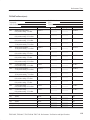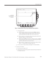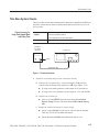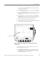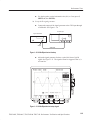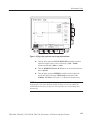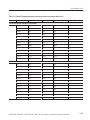
1
Technical Reference
TDS 500D, TDS 600C, TDS 700D & TDS 714L
Digitizing Oscilloscopes
Performance Verification and Specifications
071-0630-03
www.tektronix.com
Copyright © Tektronix, Inc. All rights reserved.
Tektronix products are covered by U.S. and foreign patents, issued and pending. Information in this publication supercedes
that in all previously published material. Specifications and price change privileges reserved.
Tektronix, Inc., P.O. Box 500, Beaverton, OR 97077
TEKTRONIX and TEK are registered trademarks of Tektronix, Inc.
WARRANTY
Tektronix warrants that this product will be free from defects in materials and workmanship for a period of three (3) years
from the date of shipment. If any such product proves defective during this warranty period, Tektronix, at its option, either
will repair the defective product without charge for parts and labor, or will provide a replacement in exchange for the
defective product.
In order to obtain service under this warranty, Customer must notify Tektronix of the defect before the expiration of the
warranty period and make suitable arrangements for the performance of service. Customer shall be responsible for
packaging and shipping the defective product to the service center designated by Tektronix, with shipping charges prepaid.
Tektronix shall pay for the return of the product to Customer if the shipment is to a location within the country in which the
Tektronix service center is located. Customer shall be responsible for paying all shipping charges, duties, taxes, and any
other charges for products returned to any other locations.
This warranty shall not apply to any defect, failure or damage caused by improper use or improper or inadequate
maintenance and care. Tektronix shall not be obligated to furnish service under this warranty a) to repair damage resulting
from attempts by personnel other than Tektronix representatives to install, repair or service the product; b) to repair
damage resulting from improper use or connection to incompatible equipment; or c) to service a product that has been
modified or integrated with other products when the effect of such modification or integration increases the time or
difficulty of servicing the product.
THIS WARRANTY IS GIVEN BY TEKTRONIX WITH RESPECT TO THIS PRODUCT IN LIEU OF ANY
OTHER WARRANTIES, EXPRESSED OR IMPLIED. TEKTRONIX AND ITS VENDORS DISCLAIM ANY
IMPLIED WARRANTIES OF MERCHANTABILITY OR FITNESS FOR A PARTICULAR PURPOSE.
TEKTRONIX’ RESPONSIBILITY TO REPAIR OR REPLACE DEFECTIVE PRODUCTS IS THE SOLE AND
EXCLUSIVE REMEDY PROVIDED TO THE CUSTOMER FOR BREACH OF THIS WARRANTY. TEKTRONIX
AND ITS VENDORS WILL NOT BE LIABLE FOR ANY INDIRECT, SPECIAL, INCIDENTAL, OR
CONSEQUENTIAL DAMAGES IRRESPECTIVE OF WHETHER TEKTRONIX OR THE VENDOR HAS
ADVANCE NOTICE OF THE POSSIBILITY OF SUCH DAMAGES.
Table of Contents
General Safety Summary . . . . . . . . . . . . . . . . . . . . . . . . . . . . . . . . . . . .
Preface . . . . . . . . . . . . . . . . . . . . . . . . . . . . . . . . . . . . . . . . . . . . . . . . . . .
v
vii
Contacting Tektronix . . . . . . . . . . . . . . . . . . . . . . . . . . . . . . . . . . . . . . . . . . . . . .
viii
Performance Verification Procedures
Input Channels versus Model . . . . . . . . . . . . . . . . . . . . . . . . . . . . . . . . . . . . . . . .
Conventions . . . . . . . . . . . . . . . . . . . . . . . . . . . . . . . . . . . . . . . . . . . . . . . . . . . . .
1–2
1–2
Brief Procedures . . . . . . . . . . . . . . . . . . . . . . . . . . . . . . . . . . . . . . . . . . .
1–5
Self Tests . . . . . . . . . . . . . . . . . . . . . . . . . . . . . . . . . . . . . . . . . . . . . . . . . . . . . . .
Functional Tests . . . . . . . . . . . . . . . . . . . . . . . . . . . . . . . . . . . . . . . . . . . . . . . . . .
1–5
1–7
Performance Tests . . . . . . . . . . . . . . . . . . . . . . . . . . . . . . . . . . . . . . . . . .
1–17
Prerequisites . . . . . . . . . . . . . . . . . . . . . . . . . . . . . . . . . . . . . . . . . . . . . . . . . . . . .
Equipment Required . . . . . . . . . . . . . . . . . . . . . . . . . . . . . . . . . . . . . . . . . . . . . . .
TDS 600C Test Record . . . . . . . . . . . . . . . . . . . . . . . . . . . . . . . . . . . . . . . . . . . .
TDS 500D/700D/714L Test Record . . . . . . . . . . . . . . . . . . . . . . . . . . . . . . . . . . .
TDS 694C Test Record . . . . . . . . . . . . . . . . . . . . . . . . . . . . . . . . . . . . . . . . . . . .
TDS 794D Test Record . . . . . . . . . . . . . . . . . . . . . . . . . . . . . . . . . . . . . . . . . . . .
Signal Acquisition System Checks . . . . . . . . . . . . . . . . . . . . . . . . . . . . . . . . . . .
Time Base System Checks . . . . . . . . . . . . . . . . . . . . . . . . . . . . . . . . . . . . . . . . . .
Trigger System Checks . . . . . . . . . . . . . . . . . . . . . . . . . . . . . . . . . . . . . . . . . . . .
Output Signal Checks . . . . . . . . . . . . . . . . . . . . . . . . . . . . . . . . . . . . . . . . . . . . . .
Option 05 Video Trigger Checks
(Not Available on TDS 694C or TDS 794D) . . . . . . . . . . . . . . . . . . . . . . . .
Sine Wave Generator Leveling Procedure . . . . . . . . . . . . . . . . . . . . . . . . . . . . . .
Optical Filter Checks (Options 2C, 3C & 4C Only) . . . . . . . . . . . . . . . . . . . . . .
1–17
1–18
1–21
1–25
1–29
1–32
1–35
1–53
1–59
1–68
1–77
1–94
1–97
Product Description . . . . . . . . . . . . . . . . . . . . . . . . . . . . . . . . . . . . . . . . . . . . . . .
User Interface . . . . . . . . . . . . . . . . . . . . . . . . . . . . . . . . . . . . . . . . . . . . . . . . . . . .
Signal Acquisition System . . . . . . . . . . . . . . . . . . . . . . . . . . . . . . . . . . . . . . . . . .
Horizontal System . . . . . . . . . . . . . . . . . . . . . . . . . . . . . . . . . . . . . . . . . . . . . . . .
Trigger System . . . . . . . . . . . . . . . . . . . . . . . . . . . . . . . . . . . . . . . . . . . . . . . . . . .
Acquisition Control . . . . . . . . . . . . . . . . . . . . . . . . . . . . . . . . . . . . . . . . . . . . . . .
On-Board User Assistance . . . . . . . . . . . . . . . . . . . . . . . . . . . . . . . . . . . . . . . . . .
Measurement Assistance . . . . . . . . . . . . . . . . . . . . . . . . . . . . . . . . . . . . . . . . . . .
Storage . . . . . . . . . . . . . . . . . . . . . . . . . . . . . . . . . . . . . . . . . . . . . . . . . . . . . . . . .
I/O . . . . . . . . . . . . . . . . . . . . . . . . . . . . . . . . . . . . . . . . . . . . . . . . . . . . . . . . . . . .
Display . . . . . . . . . . . . . . . . . . . . . . . . . . . . . . . . . . . . . . . . . . . . . . . . . . . . . . . . .
2–1
2–2
2–3
2–3
2–5
2–6
2–7
2–7
2–8
2–8
2–9
Specifications
Nominal Traits . . . . . . . . . . . . . . . . . . . . . . . . . . . . . . . . . . . . . . . . . . . . .
Warranted Characteristics . . . . . . . . . . . . . . . . . . . . . . . . . . . . . . . . . . .
Typical Characteristics . . . . . . . . . . . . . . . . . . . . . . . . . . . . . . . . . . . . . .
TDS 500D, TDS 600C, TDS 700D & TDS 714L Performance Verification and Specifications
2–11
2–19
2–29
i
Table of Contents
List of Figures
Figure 1–1: Map of display functions . . . . . . . . . . . . . . . . . . . . . . . . . .
Figure 1–2: Verifying adjustments and signal-path compensation . .
Figure 1–3: Universal test hookup for functional tests – TDS 600C
shown . . . . . . . . . . . . . . . . . . . . . . . . . . . . . . . . . . . . . . . . . . . . . . . . .
Figure 1–4: Measurement of DC offset accuracy at zero
setting – TDS 684C shown . . . . . . . . . . . . . . . . . . . . . . . . . . . . . . . .
Figure 1–5: Initial test hookup . . . . . . . . . . . . . . . . . . . . . . . . . . . . . . . .
Figure 1–6: Measurement of DC accuracy at maximum offset
and position . . . . . . . . . . . . . . . . . . . . . . . . . . . . . . . . . . . . . . . . . . . .
Figure 1–7: Initial test hookup . . . . . . . . . . . . . . . . . . . . . . . . . . . . . . . .
Figure 1–8: Optional initial test hookup . . . . . . . . . . . . . . . . . . . . . . . .
Figure 1–9: Measurement of analog bandwidth . . . . . . . . . . . . . . . . . .
Figure 1–10: Initial test hookup . . . . . . . . . . . . . . . . . . . . . . . . . . . . . . .
Figure 1–11: Measurement of channel delay – TDS 684C shown . . . .
Figure 1–12: Initial test hookup . . . . . . . . . . . . . . . . . . . . . . . . . . . . . . .
Figure 1–13: Measurement of accuracy – long-term and delay time .
Figure 1–14: Delta time accuracy test hookup . . . . . . . . . . . . . . . . . . .
Figure 1–15: Initial test hookup . . . . . . . . . . . . . . . . . . . . . . . . . . . . . . .
Figure 1–16: Measurement of time accuracy for pulse and glitch
triggering . . . . . . . . . . . . . . . . . . . . . . . . . . . . . . . . . . . . . . . . . . . . .
Figure 1–17: Initial test hookup . . . . . . . . . . . . . . . . . . . . . . . . . . . . . . .
Figure 1–18: Measurement of trigger sensitivity – 50 MHz results
shown on a TDS 684C screen . . . . . . . . . . . . . . . . . . . . . . . . . . . . . .
Figure 1–19: Initial test hookup . . . . . . . . . . . . . . . . . . . . . . . . . . . . . . .
Figure 1–20: Measurement of main trigger out limits . . . . . . . . . . . . .
Figure 1–21: Initial test hookup . . . . . . . . . . . . . . . . . . . . . . . . . . . . . . .
Figure 1–22: Measurement of probe compensator frequency . . . . . . .
Figure 1–23: Subsequent test hookup . . . . . . . . . . . . . . . . . . . . . . . . . .
Figure 1–24: Measurement of probe compensator amplitude . . . . . .
Figure 1–25: Jitter test hookup . . . . . . . . . . . . . . . . . . . . . . . . . . . . . . .
Figure 1–26: Jitter test displayed waveform – TDS 754D shown . . . .
Figure 1–27: Jitter test when completed – TDS 754D shown . . . . . . .
Figure 1–28: Triggered signal range test – 300 mV . . . . . . . . . . . . . . .
Figure 1–29: Triggered signal range test – 75 mV . . . . . . . . . . . . . . . .
Figure 1–30: 60 Hz Rejection test hookup . . . . . . . . . . . . . . . . . . . . . .
Figure 1–31: 60 Hz Rejection test setup signal . . . . . . . . . . . . . . . . . . .
ii
1–3
1–6
1–8
1–37
1–38
1–41
1–43
1–43
1–46
1–49
1–51
1–53
1–55
1–56
1–60
1–61
1–64
1–65
1–68
1–70
1–73
1–74
1–75
1–76
1–78
1–79
1–80
1–81
1–82
1–83
1–83
TDS 500D, TDS 600C, TDS 700D & TDS 714L Performance Verification and Specifications
Table of Contents
Figure 1–32: Subsequent 60 Hz Rejection test hookup . . . . . . . . . . . .
1–84
Figure 1–33: 60 Hz Rejection test result – TDS 684C shown . . . . . . .
1–85
Figure 1–34: Line count accuracy test hookup . . . . . . . . . . . . . . . . . . .
1–86
Figure 1–35: Line count accuracy test setup waveform –
TDS 684C shown . . . . . . . . . . . . . . . . . . . . . . . . . . . . . . . . . . . . . . . .
1–87
Figure 1–36: Line count accuracy correct result waveform . . . . . . . .
1–88
Figure 1–37: Setup for sync duty cycle test . . . . . . . . . . . . . . . . . . . . . .
1–90
Figure 1–38: Sync duty cycle test: one-div neg pulse waveform . . . . .
1–91
Figure 1–39: Sync duty cycle test: critically adjusted pulse . . . . . . . .
1–92
Figure 1–40: Sine wave generator leveling equipment setup . . . . . . .
1–94
Figure 1–41: Equipment setup for maximum amplitude . . . . . . . . . .
1–96
Figure 1–42: Reference-receiver performance-verification set up . . .
1–99
Figure 1–43: Optical impulse of Ch1 input from OA5022 Optical
Attenuator (OIG501 / OIG502 fed into optical attenuator
in Step 1) . . . . . . . . . . . . . . . . . . . . . . . . . . . . . . . . . . . . . . . . . . . . . . 1–101
Figure 1–44: Optical impulse response for OC–12 SONET Reference
Receiver . . . . . . . . . . . . . . . . . . . . . . . . . . . . . . . . . . . . . . . . . . . . . . . 1–104
Figure 1–45: Optical impulse response for OC–12 SONET Reference
Receiver . . . . . . . . . . . . . . . . . . . . . . . . . . . . . . . . . . . . . . . . . . . . . . . 1–105
TDS 500D, TDS 600C, TDS 700D & TDS 714L Performance Verification and Specifications
iii
Table of Contents
List of Tables
Table 1–1: Test equipment . . . . . . . . . . . . . . . . . . . . . . . . . . . . . . . . . . .
1–18
Table 1–2: DC offset accuracy (zero setting) . . . . . . . . . . . . . . . . . . . .
1–36
Table 1–3: DC Voltage measurement accuracy . . . . . . . . . . . . . . . . . .
1–40
Table 1–4: Analog bandwidth . . . . . . . . . . . . . . . . . . . . . . . . . . . . . . . .
1–45
Table 1–5: Delay between channels worksheet . . . . . . . . . . . . . . . . . .
1–52
Table 1–6: Delta time measurement . . . . . . . . . . . . . . . . . . . . . . . . . . .
1–58
Table 1–7: Available filters . . . . . . . . . . . . . . . . . . . . . . . . . . . . . . . . . . .
1–97
Table 1–8: Reference receiver filter options . . . . . . . . . . . . . . . . . . . . .
1–97
Table 1–9: Option 3C and 4C specifications . . . . . . . . . . . . . . . . . . . .
1–98
Table 1–10: Available receivers . . . . . . . . . . . . . . . . . . . . . . . . . . . . . . .
1–98
Table 1–11: Bessel Thompson frequency response and reference receiver
limits . . . . . . . . . . . . . . . . . . . . . . . . . . . . . . . . . . . . . . . . . . . . . . . . . 1–106
Table 2–1: Key features of TDS 500D, 600C, 700D and 714L
oscilloscopes . . . . . . . . . . . . . . . . . . . . . . . . . . . . . . . . . . . . . . . . . . .
Table 2–2: Record length and divisions per record versus
TDS model . . . . . . . . . . . . . . . . . . . . . . . . . . . . . . . . . . . . . . . . . . . .
Table 2–3: Nominal traits — Signal acquisition system . . . . . . . . . . .
Table 2–4: Nominal traits — Time base system . . . . . . . . . . . . . . . . . .
Table 2–5: Nominal traits — Triggering system . . . . . . . . . . . . . . . . .
Table 2–6: Nominal traits — Display system . . . . . . . . . . . . . . . . . . . .
Table 2–7: Nominal traits — GPIB interface, output ports, and
power fuse . . . . . . . . . . . . . . . . . . . . . . . . . . . . . . . . . . . . . . . . . . . . .
Table 2–8: Nominal traits — Data handling and reliability . . . . . . . .
Table 2–9: Nominal traits — Mechanical . . . . . . . . . . . . . . . . . . . . . . .
Table 2–10: Warranted characteristics — Signal acquisition system
Table 2–11: Warranted characteristics — Time base system . . . . . . .
Table 2–12: Warranted characteristics — Triggering system . . . . . .
Table 2–13: Warranted characteristics — Output ports, probe
compensator, and power requirements . . . . . . . . . . . . . . . . . . . . .
Table 2–14: Warranted characteristics — Environmental . . . . . . . . .
Table 2–15: Certifications and compliances . . . . . . . . . . . . . . . . . . . . .
Table 2–16: Typical characteristics — Signal acquisition system . . .
Table 2–17: Typical characteristics — Time base system . . . . . . . . . .
Table 2–18: Typical characteristics — Triggering system . . . . . . . . .
iv
2–1
2–4
2–11
2–12
2–13
2–15
2–16
2–16
2–17
2–20
2–22
2–23
2–24
2–25
2–27
2–29
2–32
2–33
TDS 500D, TDS 600C, TDS 700D & TDS 714L Performance Verification and Specifications
General Safety Summary
Review the following safety precautions to avoid injury and prevent damage to
this product or any products connected to it. To avoid potential hazards, use this
product only as specified.
Only qualified personnel should perform service procedures.
While using this product, you may need to access other parts of the system. Read
the General Safety Summary in other system manuals for warnings and cautions
related to operating the system.
To Avoid Fire or
Personal Injury
Use Proper Power Cord. Use only the power cord specified for this product and
certified for the country of use.
Ground the Product. This product is grounded through the grounding conductor
of the power cord. To avoid electric shock, the grounding conductor must be
connected to earth ground. Before making connections to the input or output
terminals of the product, ensure that the product is properly grounded.
Connect and Disconnect Properly. Do not connect or disconnect probes or test
leads while they are connected to a voltage source.
Do Not Operate Without Covers. Do not operate this product with covers or panels
removed.
Use Proper Fuse. Use only the fuse type and rating specified for this product.
Do Not Operate in Wet/Damp Conditions.
Do Not Operate in an Explosive Atmosphere.
Observe All Terminal Ratings. To avoid fire or shock hazard, observe all ratings
and markings on the product. Consult the product manual for further ratings
information before making connections to the product.
Do not apply a potential to any terminal, including the common terminal, that
exceeds the maximum rating of that terminal.
Use Proper Power Source. Do not operate this product from a power source that
applies more than the voltage specified.
Provide Proper Ventilation. Refer to the manual’s installation instructions for
details on installing the product so it has proper ventilation.
Do Not Operate With Suspected Failures. If you suspect there is damage to this
product, have it inspected by qualified service personnel.
TDS 500D, TDS 600C, TDS 700D & TDS 714L Performance Verification and Specifications
v
General Safety Summary
Product Damage
Precautions
Electrostatic Discharge. Acquisition circuitry in the TDS 694C/794D is very
susceptible to damage from electrostatic discharge and from overdrive signals.
To prevent electrostatic damage to the TDS 694C/794D, be sure to operate the
oscilloscope only in a static-controlled environment. Be sure to discharge to
ground any electrostatic charge that may be present on cables and probes before
attaching them to the oscilloscope.
To prevent damage from electrostatic discharge, install short-circuit terminations
on unused input connectors. Always use a wrist strap with internal impedance
(provided with your instrument) when handling your oscilloscope or making
connections.
Symbols and Terms
Terms in this Manual. These terms may appear in this manual:
WARNING. Warning statements identify conditions or practices that could result
in injury or loss of life.
CAUTION. Caution statements identify conditions or practices that could result in
damage to this product or other property.
Terms on the Product. These terms may appear on the product:
DANGER indicates an injury hazard immediately accessible as you read the
marking.
WARNING indicates an injury hazard not immediately accessible as you read the
marking.
CAUTION indicates a hazard to property including the product.
Symbols on the Product. The following symbols may appear on the product:
WARNING
High Voltage
Certifications and
Compliances
vi
Protective Ground
(Earth) Terminal
CAUTION
Refer to Manual
Double
Insulated
CSA Certified Power Cords. CSA Certification includes the products and power
cords appropriate for use in the North America power network. All other power
cords supplied are approved for the country of use.
TDS 500D, TDS 600C, TDS 700D & TDS 714L Performance Verification and Specifications
Preface
This is the Performance Verification and Specifications for the TDS 500D,
TDS 600C, TDS 700D, and TDS 714L Oscilloscopes. It contains procedures
suitable for determining if each instrument functions, was adjusted properly, and
meets the performance characteristics as warranted. The following models are
covered:
TDS 500:
TDS 520D, TDS 540D and TDS 580D
TDS 600:
TDS 654C, TDS 680C, TDS 684C and TDS 694C
TDS 700:
TDS 714L, TDS 724D, TDS 754D, TDS 784D, and
TDS 794D
This document also contains the technical specifications for these oscilloscopes.
Related Manuals
The following documents are related to the use or service of this oscilloscope:
H
The TDS 500D, TDS 600B & TDS 700D User Manual describes how to use
this oscilloscope.
H
The TDS Family Programmer Disk, included with the User Manual,
describes using a computer to control the oscilloscope through the GPIB
interface.
H
The TDS 500D, TDS 600B & TDS 700D Reference describes a quick
overview of how to operate your oscilloscope.
H
The TDS 500D, TDS 600C, TDS 700D & TDS 714L Service Manual
describes information for maintaining and servicing the oscilloscope to the
module level.
TDS 500D, TDS 600C, TDS 700D & TDS 714L Performance Verification and Specifications
vii
Preface
Contacting Tektronix
Phone
1-800-833-9200*
Address
Tektronix, Inc.
Department or name (if known)
14200 SW Karl Braun Drive
P.O. Box 500
Beaverton, OR 97077
USA
Web site
www.tektronix.com
Sales support
1-800-833-9200, select option 1*
Service support
1-800-833-9200, select option 2*
Technical support
Email: [email protected]
1-800-833-9200, select option 3*
1-503-627-2400
6:00 a.m. – 5:00 p.m. Pacific time
*
viii
This phone number is toll free in North America. After office hours, please leave a
voice mail message.
Outside North America, contact a Tektronix sales office or distributor; see the
Tektronix web site for a list of offices.
TDS 500D, TDS 600C, TDS 700D & TDS 714L Performance Verification and Specifications
Performance Verification
Procedures
Performance Verification Procedures
Two types of Performance Verification procedures can be performed on this
product: Brief Procedures and Performance Tests. You may not need to perform
all of these procedures, depending on what you want to accomplish.
H
To rapidly confirm that the oscilloscope functions and was adjusted properly,
just do the brief procedures under Self Tests, which begin on page 1–5.
Advantages: These procedures are quick to do, require no external
equipment or signal sources, and perform extensive functional and accuracy
testing to provide high confidence that the oscilloscope will perform
properly. They can be used as a quick check before making a series of
important measurements.
H
To further check functionality, first do the Self Tests just mentioned; then do
the brief procedures under Functional Tests that begin on page 1–7.
Advantages: These procedures require minimal additional time to perform,
require no additional equipment other than a standard-accessory probe, and
more completely test the internal hardware of the oscilloscope. They can be
used to quickly determine if the oscilloscope is suitable for putting into
service, such as when it is first received.
H
If more extensive confirmation of performance is desired, do the Performance Tests, beginning on page 1–17, after doing the Functional and Self Tests
just referenced.
Advantages: These procedures add direct checking of warranted specifications. They require more time to perform and suitable test equipment is
required. (See Equipment Required beginning on page 1–18).
If you are not familiar with operating this oscilloscope, read the oscilloscope
reference or user manuals. These contain instructions that will acquaint you with
the use of the front-panel controls and the menu system.
TDS 500D, TDS 600C, TDS 700D & TDS 714L Performance Verification and Specifications
1–1
Performance Verification Procedures
Input Channels versus Model
When performing the procedures in this section, be aware that some TDS models
refer to input channels Ch 3 and Ch 4 as Aux 1 and Aux 2 respectively. Where
appropriate, both names will appear in the procedure, for example, Ch 3 (Aux 1).
The channel names for the various TDS models are shown below.
TDS Model
Channel Names
TDS 540D, 580D, 654C, 684C, 694C, 714L, 754D,
784D, and 794D
Ch 1, Ch 2, Ch 3, and Ch 4
TDS 520D, 680C, and 724D
Ch 1, Ch 2, Aux 1, and Aux 2
Conventions
Throughout these procedures the following conventions apply:
H
Each test procedure uses the following general format:
Title of Test
Equipment Required
Prerequisites
Procedure
H
Each procedure consists of as many steps, substeps, and subparts as required
to do the test. Steps, substeps, and subparts are sequenced as follows:
1. First Step
a. First Substep
H
First Subpart
H
Second Subpart
b. Second Substep
2. Second Step
H
1–2
In steps and substeps, the lead-in statement in italics instructs you what to
do, while the instructions that follow tell you how to do it, as in the example
step below, “Initialize the oscilloscope” by doing “Press save/recall SETUP.
Now, press the main-menu button...”.
TDS 500D, TDS 600C, TDS 700D & TDS 714L Performance Verification and Specifications
Performance Verification Procedures
Initialize the oscilloscope: Press save/recall SETUP. Now, press the
main-menu button Recall Factory Setup; then the side-menu button OK
Confirm Factory Init.
H
Where instructed to use a front-panel button or knob, or select from a main
or side menu, or verify a readout or status message, the name of the button or
knob appears in boldface type: “press SHIFT; then UTILITY, press the
main-menu button System until Cal is highlighted in the pop-up menu.
Verify that the status message is Pass in the main menu under the Voltage
Reference label.”
STOP. The STOP notation at the left is accompanied by information you must read
to do the procedure properly.
H
Refer to Figure 1–1: “Main menu” refers to the menu that labels the seven
menu buttons under the display; “side menu” refers to the menu that labels
the five buttons to the right of the display. “Pop-up menu” refers to a menu
that pops up when a main-menu button is pressed.
Position of waveform
record relative to
the screen and display
General purpose
knob readout
Brief status
information
Side menu area.
Readouts for
measurements
move here when
CLEAR MENU
is pressed.
Graticule and waveforms
Waveform reference
symbols show ground levels
and waveform sources
Vertical scale, horizontal scale,
and trigger level readouts
Pop-up menu
Main menu display area. Readouts in lower graticule
area move here when CLEAR MENU is pressed.
Figure 1–1: Map of display functions
TDS 500D, TDS 600C, TDS 700D & TDS 714L Performance Verification and Specifications
1–3
Performance Verification Procedures
1–4
TDS 500D, TDS 600C, TDS 700D & TDS 714L Performance Verification and Specifications
Brief Procedures
The Self Tests use internal routines to confirm basic functionality and proper
adjustment. No test equipment is required to do these test procedures.
The Functional Tests utilize the probe-compensation output at the front panel as
a test-signal source for further verifying that the oscilloscope functions properly.
A probe is required to do these test procedures.
Self Tests
This procedure uses internal routines to verify that the oscilloscope functions and
was adjusted properly. No test equipment or hookups are required.
Verify Internal Adjustment,
Self Compensation, and
Diagnostics
Equipment
required
None
Prerequisites
Power on the oscilloscope and allow a 20 minute warm-up before doing
this procedure.
1. Verify that internal diagnostics pass: Do the following substeps to verify
passing of internal diagnostics.
a. Display the System diagnostics menu:
H
Press SHIFT; then press UTILITY.
H
Repeatedly press the main-menu button System until Diag/Err is
highlighted in the pop-up menu.
b. Run the System Diagnostics:
H
First disconnect any input signals from all four channels.
H
Press the main-menu button Execute; then press the side-menu
button OK Confirm Run Test.
c. Wait: The internal diagnostics do an exhaustive verification of proper
oscilloscope function. This verification will take up to three and a half
minutes on some models. When the verification is finished, the resulting
status will appear on the screen.
d. Verify that no failures are found and reported on-screen. If any failures
occur do step 1a, then press the main menu button Error Log for details.
e. Confirm the three adjustment sections have passed status:
TDS 500D, TDS 600C, TDS 700D & TDS 714L Performance Verification and Specifications
1–5
Brief Procedures
f.
H
Press SHIFT; then press UTILITY.
H
Highlight Cal in the pop-up menu by repeatedly pressing the
main-menu button System. See Figure 1–2.
H
Verify that the word Pass appears in the main menu under the
following menu labels: Voltage Reference, Frequency Response,
and Pulse Trigger. See Figure 1–2.
Run the signal-path compensation: Press the main-menu button Signal
Path; then press the side-menu button OK Compensate Signal Paths.
g. Wait: Signal-path compensation may take five to fifteen minutes to run.
While it progresses, a “clock” icon (shown at left) is displayed onscreen. When compensation completes, the status message will be
updated to Pass or Fail in the main menu. See step h.
h. Confirm signal-path compensation returns passed status: Verify that the
word Pass appears under Signal Path in the main menu. See Figure 1–2.
Highlight Cal
1
3
2
Verify Pass
Verify Pass
Figure 1–2: Verifying adjustments and signal-path compensation
2. Return to regular service: Press CLEAR MENU to exit the system menus.
1–6
TDS 500D, TDS 600C, TDS 700D & TDS 714L Performance Verification and Specifications
Brief Procedures
Functional Tests
The purpose of these procedures is to confirm that the oscilloscope functions
properly. The only equipment required is one of the standard-accessory probes
and, to check the file system, a 3.5 inch, 720 K or 1.44 Mbyte floppy disk.
CAUTION. The P6243, P6245, P6249 and probes that can be used with this
oscilloscope provide an extremely low loading capacitance (<1 pF) to ensure the
best possible signal reproduction. These probes should not be used to measure
signals exceeding ±8 volts, or errors in signal measurement will be observed.
Above 40 volts, damage to the probe may result. To make measurements beyond
±10 volts, use either the P6139A probe (good to 500 volts peak), the P6339A
probe (for the TDS 694C & TDS 794D), or refer to the catalog for a recommended probe.
STOP. These procedures verify functions; that is, they verify that the oscilloscope
features operate. They do not verify that they operate within limits.
Therefore, when the instructions in the functional tests that follow call for you to
verify that a signal appears on-screen “that is about five divisions in amplitude”
or “has a period of about six horizontal divisions,” etc., do NOT interpret the
quantities given as limits. Operation within limits is checked in Performance
Tests, which begin on page 1–17.
STOP. DO NOT make changes to the front-panel settings that are not called out
in the procedures. Each verification procedure will require you to set the
oscilloscope to certain default settings before verifying functions. If you make
changes to these settings, other than those called out in the procedure, you may
obtain invalid results. In this case, just redo the procedure from step 1.
When you are instructed to press a menu button, the button may already be
selected (its label will be highlighted). If this is the case, it is not necessary to
press the button.
TDS 500D, TDS 600C, TDS 700D & TDS 714L Performance Verification and Specifications
1–7
Brief Procedures
Verify All Input Channels
Equipment
required
One probe such as the P6243, P6245, P6249, P6139A1, or P6339A
Prerequisites
None
1
P6139A probe is not appropriate for the TDS694C/794D oscilloscopes.
1. Install the test hookup and preset the oscilloscope controls:
a. Hook up the signal source: Install the probe on CH 1. Connect the probe
tip to PROBE COMPENSATION SIGNAL on the front panel;
connect the probe ground (typically black) to PROBE COMPENSATION GND. If using a P6243, P6245 or P6249 probe, you may want to
attach a Y-lead connector and two SMD KlipChips as shown in
Figure 1–3.
Signal
Gnd
Figure 1–3: Universal test hookup for functional tests – TDS 600C shown
b. Initialize the oscilloscope:
1–8
H
Press save/recall SETUP.
H
Press the main-menu button Recall Factory Setup.
H
Press the side-menu button OK Confirm Factory Init.
TDS 500D, TDS 600C, TDS 700D & TDS 714L Performance Verification and Specifications
Brief Procedures
2. Verify that all channels operate: Do the following substeps — test CH 1
first, skipping substep a and b since CH 1 is already set up for verification
and as the trigger source from step 1.
a. Select an unverified channel:
H
Press WAVEFORM OFF to remove the channel just verified from
display.
H
Press the front-panel button that corresponds to the channel you are
to verify.
H
Move the probe to the channel you selected.
b. Match the trigger source to the channel selected:
H
Press TRIGGER MENU.
H
Press the main-menu button Source.
H
Press the side-menu button that corresponds to the channel selected,
Ch2, Ch3, or Ch4. (Some TDS models use Ax1 and Ax2 instead of
Ch3 and Ch4).
c. Set up the selected channel:
H
Set the vertical SCALE to 200 mV.
H
Set the horizontal SCALE to 200 ms. Press CLEAR MENU to
remove any menu that may be on the screen.
H
Press SET LEVEL TO 50%.
d. Verify that the channel is operational: Confirm that the following
statements are true.
H
The vertical scale readout for the channel under test shows a setting
of 200 mV, and a square-wave probe-compensation signal about
2.5 divisions in amplitude is on-screen. See Figure 1–1 on page 1–3
to locate the readout.
H
The vertical POSITION knob moves the signal up and down the
screen when rotated.
H
Turning the vertical SCALE knob counterclockwise decreases the
amplitude of the waveform on-screen, turning the knob clockwise
increases the amplitude, and returning the knob to 200 mV returns
the amplitude to about 2.5 divisions.
TDS 500D, TDS 600C, TDS 700D & TDS 714L Performance Verification and Specifications
1–9
Brief Procedures
e. Verify that the channel acquires in all acquisition modes: Press SHIFT;
then press ACQUIRE MENU. Use the side menu to select, in turn, each
of the three hardware acquire modes and confirm that the following
statements are true. Refer to the icons at the left of each statement as you
confirm those statements.
f.
H
Sample mode displays an actively acquiring waveform on-screen.
(Note that there is noise present on the peaks of the square wave).
H
Peak Detect mode displays an actively acquiring waveform
on-screen with the noise present in Sample mode “peak detected.”
H
Hi Res mode (TDS 500D and 700D/L only) displays an actively
acquiring waveform on-screen with the noise that was present in
Sample mode reduced.
H
Envelope mode displays an actively acquiring waveform on-screen
with the noise displayed.
H
Average mode displays an actively acquiring waveform on-screen
with the noise reduced.
Test all channels: Repeat substeps a through e until all four input
channels are verified.
3. Remove the test hookup: Disconnect the probe from the channel input and
the probe-compensation terminals.
Verify the Time Base
Equipment
required
One probe such as the P6243, P6245, P6249, P6139A1, or P6339A
Prerequisites
None
1
P6139A probe is not appropriate for the TDS694C/794D oscilloscopes.
1. Install the test hookup and preset the oscilloscope controls:
a. Hook up the signal source: Install the probe on CH 1. Connect the probe
tip to PROBE COMPENSATION SIGNAL on the front panel;
connect the probe ground to PROBE COMPENSATION GND. See
Figure 1–3 on page 1–8.
b. Initialize the oscilloscope:
H
Press save/recall SETUP.
H
Press the main-menu button Recall Factory Setup; then press the
side-menu button OK Confirm Factory Init.
c. Modify default settings:
1–10
TDS 500D, TDS 600C, TDS 700D & TDS 714L Performance Verification and Specifications
Brief Procedures
H
Set the vertical SCALE to 200 mV.
H
Set the horizontal SCALE to 200 ms.
H
Press SET LEVEL TO 50%.
H
Press CLEAR MENU to remove the menus from the screen.
2. Verify that the time base operates: Confirm the following statements.
a. One period of the square-wave probe-compensation signal is about five
horizontal divisions on-screen for the 200 ms horizontal scale setting (set
in step 1c).
b. Rotating the horizontal SCALE knob clockwise expands the waveform
on-screen (more horizontal divisions per waveform period), counterclockwise rotation contracts it, and returning the horizontal scale to
200 ms returns the period to about five divisions.
c. The horizontal POSITION knob positions the signal left and right
on-screen when rotated.
3. Remove the test hookup: Disconnect the probe from the channel input and
the probe-compensation terminals.
Verify the Main and
Delayed Trigger Systems
Equipment
required
One probe such as the P6243, P6245, P6249, P6139A1, or P6339A
Prerequisites
None
1
P6139A probe is not appropriate for the TDS694C/794D oscilloscopes.
1. Install the test hookup and preset the oscilloscope controls:
a. Hook up the signal source: Install the probe on CH 1. Connect the probe
tip to PROBE COMPENSATION SIGNAL on the front panel;
connect the probe ground to PROBE COMPENSATION GND. See
Figure 1–3 on page 1–8.
b. Initialize the oscilloscope:
H
Press save/recall SETUP.
H
Press the main-menu button Recall Factory Setup.
H
Press the side-menu button OK Confirm Factory Init.
c. Modify default settings:
H
Set the vertical SCALE to 200 mV.
H
Set the horizontal SCALE for the M (main) time base to 200 ms.
TDS 500D, TDS 600C, TDS 700D & TDS 714L Performance Verification and Specifications
1–11
Brief Procedures
H
Press SET LEVEL TO 50%.
H
Press TRIGGER MENU.
H
Press the main-menu button Mode & Holdoff.
H
Press the side-menu button Normal.
H
Press CLEAR MENU to remove the menus from the screen.
2. Verify that the main trigger system operates: Confirm that the following
statements are true.
H
The trigger level readout for the main trigger system changes with the
trigger-LEVEL knob.
H
The trigger-LEVEL knob can trigger and untrigger the square-wave
signal as you rotate it. (Leave the signal untriggered, which is indicated
by the display not updating).
H
Pressing SET LEVEL TO 50% triggers the signal that you just left
untriggered. (Leave the signal triggered).
3. Verify that the delayed trigger system operates:
a. Select the delayed time base:
H
Press HORIZONTAL MENU.
H
Press the main-menu button Time Base.
H
Press the side-menu button Delayed Triggerable; then press the
side-menu button Delayed Only.
H
Set the horizontal SCALE for the D (delayed) time base to 200 ms.
b. Select the delayed trigger level menu:
H
Press SHIFT; then press DELAYED TRIG.
H
Press the main-menu button Level; then press the side-menu button
Level.
c. Confirm that the following statements are true:
1–12
H
The trigger-level readout for the delayed trigger system changes as
you turn the general purpose knob.
H
As you rotate the general purpose knob, the square-wave probe-compensation signal can become triggered and untriggered. (Leave the
signal untriggered, which is indicated by the display not updating).
TDS 500D, TDS 600C, TDS 700D & TDS 714L Performance Verification and Specifications
Brief Procedures
H
Pressing the side-menu button Set to 50% triggers the probe-compensation signal that you just left untriggered. (Leave the signal
triggered).
d. Verify the delayed trigger counter:
H
Press the main-menu button Delay by Time.
H
Use the keypad to enter a delay time of 1 second. Press 1, then press
ENTER.
H
Verify that the trigger READY indicator on the front panel flashes
about once every second as the waveform is updated on-screen.
4. Remove the test hookup: Disconnect the probe from the channel input and
the probe-compensation terminals.
Verify the File System
One probe such as the P6243, P6245, P6249, P6139A1, or P6339A
Equipment
required
One 720 K or 1.44 Mbyte, 3.5 inch DOS-compatible disk.
You can use a disk of your own or you can use the TDS Family
Programmer Disk included in your user manual.
Prerequisites
1
None
P6139A probe is not appropriate for the TDS694C/794D oscilloscopes.
1. Install the test hookup and preset the oscilloscope controls:
a. Hook up the signal source: Install the probe on CH 1. Connect the probe
tip to PROBE COMPENSATION SIGNAL on the front panel;
connect the probe ground to PROBE COMPENSATION GND. See
Figure 1–3 on page 1–8.
b. Insert the test disk: Insert the floppy disk in the floppy disk drive to the
left of the monitor.
H
Position the disk so the metal shutter faces the drive.
H
Position the disk so the stamped arrow is on the top right side. In
other words, place the angled corner in the front bottom location.
H
Push the disk into the drive until it goes all the way in and clicks
into place.
c. Initialize the oscilloscope:
H
Press save/recall SETUP.
H
Press the main-menu button Recall Factory Setup.
H
Press the side-menu button OK Confirm Factory Init.
TDS 500D, TDS 600C, TDS 700D & TDS 714L Performance Verification and Specifications
1–13
Brief Procedures
d. Modify default settings:
H
Set the vertical SCALE to 200 mV.
H
Set the horizontal SCALE for the M (main) time base to 200 ms.
Notice the waveform on the display now shows two cycles instead of
five.
H
Press SET LEVEL TO 50%.
H
Press CLEAR MENU to remove the menus from the screen.
e. Save the settings:
H
Press SETUP.
H
Press the main-menu button Save Current Setup; then press the
side-menu button To File.
H
Turn the general purpose knob to select the file to save. Choose
TEK?????.SET (or fd0:, the floppy disk drive, hd0:, the optional
hard disk drive, or Zip:, if an external Zip drive is connected). With
this choice, you will save a file starting with TEK, then containing
5-numbers, and a .SET extension. For example, the first time you
run this on a blank, formatted disk or on the Example Programs
Disk, the oscilloscope will assign the name TEK00000.SET to your
file. If you ran the procedure again, the oscilloscope would
increment the name and call the file TEK00001.SET.
NOTE. If testing an external Zip drive, it must first be connected to the oscilloscope, then be powered on simultaneously with the oscilloscope, or immediately
after the oscilloscope is powered-on. This ensures proper communications are
set up between the oscilloscope and the Zip drive.
f.
To test the optional hard disk drive or external Zip drive, choose either
the hard disk drive (hd0:), or the external Zip drive (Zip:). Then use the
general purpose knob to select the file to save. Save the file as in step e.
H
Press the side-menu button Save To Selected File.
2. Verify the file system works:
1–14
H
Press the main-menu button Recall Factory Setup and the side-menu
button OK Confirm Factory Init to restore the 500 ms time base and
the five cycle waveform.
H
Press the main-menu button Recall Saved Setup; then press the
side-menu button From File.
TDS 500D, TDS 600C, TDS 700D & TDS 714L Performance Verification and Specifications
Brief Procedures
H
Turn the general purpose knob to select the file to recall. For example, if
you followed the instructions previously and saved the file to either the
floppy disk drive (fd0:), or the optional hard disk drive (hd0:), you had
the oscilloscope assign the name TEK00000.SET to your file.
H
Press the side-menu button Recall From Selected File.
H
Verify that the oscilloscope retrieved the saved setup from the disk. Do
this by noticing the horizontal SCALE for the M (main) time base is
again 200 ms and the waveform shows only two cycles just as it was
when you saved the setup.
3. Remove the test hookup:
H
Disconnect the probe from the channel input and the probe-compensation terminals.
H
Remove the floppy disk from the floppy disk drive.
TDS 500D, TDS 600C, TDS 700D & TDS 714L Performance Verification and Specifications
1–15
Brief Procedures
1–16
TDS 500D, TDS 600C, TDS 700D & TDS 714L Performance Verification and Specifications
Performance Tests
This section contains a collection of procedures for checking that the TDS 500D,
TDS 600C, TDS 700D, and TDS 714L Oscilloscopes perform as warranted.
The procedures are arranged in four logical groupings: Signal Acquisition System
Checks, Time Base System Checks, Triggering System Checks, and Output Ports
Checks. They check all the characteristics that are designated as checked in
Specifications. (The characteristics that are checked appear in boldface type
under Warranted Characteristics in Specifications).
STOP. These procedures extend the confidence level provided by the basic
procedures described on page 1–5. The basic procedures should be done first,
then these procedures performed if desired.
Prerequisites
The tests in this section comprise an extensive, valid confirmation of performance and functionality when the following requirements are met:
H
The cabinet must be installed on the oscilloscope.
H
You must have performed and passed the procedures under Self Tests, found
on page 1–5, and those under Functional Tests, found on page 1–7.
H
A signal-path compensation must have been done within the recommended
calibration interval and at a temperature within ±5_ C of the present
operating temperature. (If at the time you did the prerequisite Self Tests, the
temperature was within the limits just stated, consider this prerequisite met).
H
The oscilloscope must have been last adjusted at an ambient temperature
between +20_ C and +30_ C, must have been operating for a warm-up
period of at least 20 minutes, and must be operating at an ambient temperatures as follows: +4_ C to +40_ C for the TDS 694C, +4_ C to +45_ C for
other TDS 600C and 0_ C to +50_ C for the TDS 500D, TDS 700D, and
TDS 714L. (The warm-up requirement is usually met in the course of
meeting the Self Tests and Functional Tests prerequisites listed above).
TDS 500D, TDS 600C, TDS 700D & TDS 714L Performance Verification and Specifications
1–17
Performance Tests
Equipment Required
Procedures starting on page 1–35, use external, traceable signal sources to
directly check warranted characteristics. Table 1–1 lists the required equipment.
Table 1–1: Test equipment
Item number and
description
Minimum requirements
Example
Purpose
1.
Attenuator,10X
(two required)
Ratio: 10X; impedance 50 W; connectors: female BNC input, male BNC
output
Tektronix part number
011-0059-02
Signal Attenuation
2.
Attenuator, 5X
Ratio: 5X; impedance 50 W; connectors: female BNC input, male BNC
output
Tektronix part number
011-0060-02
Signal Attenuation
3.
Adapter, BNC female-toClip Leads
BNC female-to-Clip Leads
Tektronix part number
013-0076-00
Signal Coupling for Probe
Compensator Output Check
4.
Terminator, 50 W
Impedance 50 W; connectors: female
BNC input, male BNC output
Tektronix part number
011-0049-01
Signal Termination for
Channel Delay Test
5.
Cable, Precision 50 W
Coaxial (three required)
50 W, 36 in, male-to-male BNC
connectors
Tektronix part number
012-0482-00
Signal Interconnection
6.
Connector, Dual-Banana
(two required)
Female BNC-to-dual banana
Tektronix part number
103-0090-00
Various Accuracy Tests
7.
Connector, BNC “T”
Male BNC-to-dual female BNC
Tektronix part number
103-0030-00
Checking Trigger Sensitivity
8.
Coupler, Dual-Input
Female BNC-to-dual male BNC
Tektronix part number
067-0525-02
Checking Delay Between
Channels
9.
Generator, DC Calibration
Variable amplitude to ±104 V; accuracy to 0.1%
Data Precision 82001
Checking DC Offset, Gain,
and Measurement Accuracy
10. Generator, Calibration
500 mV square wave calibrator
amplitude; accuracy to 0.25%
Tegam/Tektronix PG 506A
Calibration Generator1,3
To check accuracy of CH 3
Signal Out
11. Generator, Time Mark
(optional)
Variable marker frequency from 10 ms
to 10 ns; accuracy within 2 ppm
Tegam/Tektronix TG 501A
Time Mark Generator1,3
Checking Sample-Rate and
Delay-time Accuracy
12. Probe, 10X
A P6139A2, P6243, P6249, P6245, or
P6339A probe4
Tektronix part number
P6139A or P6245
Signal Interconnection
TDS Family Programmer Disk
(Tektronix part number
063–3120–00), included with
User Manual (Tektronix part
number 071–0130-XX)
Checking File System Basic
Functionality
Rohde & Schwarz SMT or
SMY1,5
Checking Analog Bandwidth,
Trigger Sensitivity, Samplerate, External Clock, and
Delay-Time Accuracy
13. 3.5 inch, 720 K or
1.44 Mbyte, DOS-compatible floppy disk
14. Generator, Sine Wave
1–18
250 kHz to at least 500 MHz (higher
for higher-bandwidth scopes). Variable amplitude from 60 mV to 2 Vp-p
into 50 W. Frequency error >2.0%
TDS 500D, TDS 600C, TDS 700D & TDS 714L Performance Verification and Specifications
Performance Tests
Table 1–1: Test equipment (cont.)
Item number and
description
Minimum requirements
Example
Purpose
15. Meter, Level and Power
Sensor
Frequency range:10 MHz to the
oscilloscope bandwidth. Amplitude
range: 6 mVp-p to 2 Vp-p
Rohde & Schwarz URV 35,
with NRV-Z8 power sensor1,5
Checking Analog Bandwidth
and Trigger Sensitivity
16. Splitter, Power
Frequency range: DC to 3 GHz.
Tracking: >2.0%
Tektronix part number1,5
015-0565-00
Checking Analog Bandwidth
17. Adapter (four required)
Male N-to-female BNC
Tektronix part number
103-0045-00
Checking Analog Bandwidth
18. Adapter
Female N-to-male BNC
Tektronix part number
103-0058-00
Checking Analog Bandwidth
19. Adapter
3 SMA male-to-male
Tektronix part number
015-1012-00
Checking the delay between
channels
20. Adapter
3 SMA female-to-male BNC
Tektronix part number
015-1018-00
Checking the delay between
channels
21. Generator, Video Signal
Provides PAL compatible outputs
Tektronix TSG 121
Used to Test Video Option 05
Equipped Instruments Only
22. Oscillator, Leveled Sine
wave Generator
60 Hz Sine wave
Tegam/Tektronix SG 502
(if available)1,3
Used to Test Video Option 05
Equipped Instruments Only
Tektronix CFG280
(or Tegam/Tektronix PG 502)3
Used to Test Video Option 05
Equipped Instruments Only
23. Pulse Generator
24. Cable, Coaxial
(two required)
75 W, 36 in, male-to-male BNC
connectors
Tektronix part number
012-1338-00
Used to Test Video Option 05
Equipped Instruments Only
25. Terminator, 75 W
(two required)
Impedance 75 W; connectors: female
BNC input, male BNC output
Tektronix part number
011-0102-01
Used to Test Video Option 05
Equipped Instruments Only
26. Generator, Optical Impulse
850 nm optical impulse
Tektronix OIG501 Optical
Impulse Generator3
Checking Option 3C
27. Generator, Optical Impulse
1300 nm optical impulse
Tektronix OIG502 Optical
Impulse Generator3
Checking Option 4C
28. Cable, Coaxial
(two required)
50 W, 20 in, male-to-male SMA
connectors
Tektronix part number
174-1427-00
Used to Test Delta Time
Measurement Accuracy
29. Adapter
SMA “T”, male to 2 SMA female
Tektronix part number
015-1016-00
Used to Test Delta Time
Measurement Accuracy
30. Adapter
SMA female to BNC male
Tektronix part number
015-0572-00
Used to Test Delta Time
Measurement Accuracy
31. Adapter
BNC male to female elbow
Tektronix part number
103-0031-00
Used to Test Delta Time
Measurement Accuracy
32. Terminator
Short circuit, SMA connector
Tektronix part number
015-1021-00
Used to Test Delta Time
Measurement Accuracy
33. Attenuator, 2X
Ratio: 2X; impedance 50 W; connectors: female BNC input, male BNC
output
Tektronix part number
011-0069-02
Used to Test Delta Time
Measurement Accuracy
TDS 500D, TDS 600C, TDS 700D & TDS 714L Performance Verification and Specifications
1–19
Performance Tests
Table 1–1: Test equipment (cont.)
Item number and
description
Minimum requirements
Example
Purpose
34. Attenuator, Optical
62.5 micron optical attenuator
Tektronix OA5022 Optical
Attenuator3
Checking Option 3C and 4C
35. Cable, Fiber Optic
FC-FC fiber cable
Tektronix part number
174-2322-00
Checking Option 3C and 4C
36. Optical-to-Electrical
Converter
P6701B (used with Option 3C) or
P6703B (used with Option 4C)
optical-to-electrical converter
Tektronix part number
P6701B or P6703B
Checking Option 3C and 4C
1
You may replace items 9, 10, 11, 14, 15, 16, and 22 with a Wavetek 9100 (with options 100 and 600) for 500 MHz oscilloscopes, or a Wavetek 9500 (with option 100) and output head appropriate for the bandwidth of the oscilloscope(s) being
tested. For 3 GHz oscilloscopes use a Wavetek 9530 head.
2
P6139A probe is not appropriate for the TDS694C/794D oscilloscopes.
3
Requires a TM 500 or TM 5000 Series Power Module Mainframe. For Delta Time Measurement Accuracy use a
Wavetek 9500 or a pulse generator with a rise time as shown in Table 1–6 on page 1–58.
4
Warning: The P6243 and P6245 probes that may be used with this oscilloscope provide an extremely low loading
capacitance (<1 pF) to ensure the best possible signal reproduction. These probes should not be used to measure
signals exceeding ±8 V, or errors in signal measurement will be observed. Above 40 V, damage to the probe may result.
To make measurements beyond ±8 V, use either the P6139A probe (good to 500 V), or refer to the catalog for a recommended probe. P6139A is not an appropriate probe for the TDS 694C or TDS 794D oscilloscopes.
5
If available, you may replace items 14, 15, and 16 with the following set of equipment for bandwidths up to 1 GHz:
a Tegam/Tektronix SG503 and SG504 with SG504 leveling head.
1–20
TDS 500D, TDS 600C, TDS 700D & TDS 714L Performance Verification and Specifications
Performance Tests
TDS 600C Test Record
Photocopy this and the next three pages and use them to record the performance
test results for your TDS 600C. The TDS 694C Test Record begins on
page 1–29.
TDS 600C Test Record
Instrument Serial Number:
Temperature:
Date of Calibration:
TDS 600C Performance Test
Certificate Number:
RH %:
Technician:
Minimum
Incoming
Outgoing
Maximum
Offset Accuracy
CH1 Offset
+1 mV
+101 mV
+1.01 V
– 2.1 mV
– 75.6 mV
– 756 mV
__________
__________
__________
__________
__________
__________
+ 2.1 mV
+ 75.6 mV
+ 756 mV
CH2 Offset
+1 mV
+101 mV
+1.01 V
– 2.1 mV
– 75.6 mV
– 756 mV
__________
__________
__________
__________
__________
__________
+ 2.1 mV
+ 75.6 mV
+ 756 mV
CH3 or AX1
Offset
+1 mV
+101 mV
+1.01 V
– 2.1 mV
– 75.6 mV
– 756 mV
__________
__________
__________
__________
__________
__________
+ 2.1 mV
+ 75.6 mV
+ 756 mV
CH4 or AX2
Offset
+1 mV
+101 mV
+1.01 V
– 2.1 mV
– 75.6 mV
– 756 mV
__________
__________
__________
__________
__________
__________
+ 2.1 mV
+ 75.6 mV
+ 756 mV
DC Voltage Measurement Accuracy (Averaged)
CH1
5 mV Vert scale setting,
–5 Div position setting, +1 V offset
+ 1.0329 V
__________
__________
+ 1.0471 V
CH1
5 mV Vert scale setting,
+5 Div position setting, –1 V offset
– 1.0471 V
__________
__________
– 1.0329 V
CH1
200 mV Vert scale setting,
–5 Div position setting, +10 V offset
+ 11.4165 V
__________
__________
+ 11.7835 V
CH1
200 mV Vert scale setting,
+5 Div position setting, –10 V offset
– 11.7835 V
__________
__________
– 11.4165 V
CH1
1.01 V Vert scale setting,
–5 Div position setting, +10 V offset
+ 17.102 V
__________
__________
+ 18.899 V
CH1
1.01 V Vert scale setting,
+5 Div position setting, –10 V offset
– 18.899 V
__________
__________
– 17.102 V
CH2
5 mV Vert scale setting,
–5 Div position setting, +1 V offset
+ 1.0329 V
__________
__________
+ 1.0471 V
CH2
5 mV Vert scale setting,
+5 Div position setting, –1 V offset
– 1.0471 V
__________
__________
– 1.0329 V
CH2
200 mV Vert scale setting,
–5 Div position setting, +10 V offset
+ 11.4165 V
__________
__________
+ 11.7835 V
TDS 500D, TDS 600C, TDS 700D & TDS 714L Performance Verification and Specifications
1–21
Performance Tests
TDS 600C Test Record (cont.)
Instrument Serial Number:
Temperature:
Date of Calibration:
Certificate Number:
RH %:
Technician:
TDS 600C Performance Test
Minimum
Incoming
Outgoing
Maximum
CH2
200 mV Vert scale setting,
+5 Div position setting, –10 V offset
– 11.7835 V
__________
__________
– 11.4165 V
CH2
1.01 V Vert scale setting,
–5 Div position setting, +10 V offset
+ 17.102 V
__________
__________
+ 18.899 V
CH2
1.01 V Vert scale setting,
+5 Div position setting, –10 V offset
– 18.899 V
__________
__________
– 17.102 V
CH3
or AX1
5 mV Vert scale setting,
–5 Div position setting, +1 V offset
+ 1.0329 V
__________
__________
+ 1.0471 V
CH3
or AX1
5 mV Vert scale setting,
+5 Div position setting, –1 V offset
– 1.0471 V
__________
__________
– 1.0329 V
CH3
or AX1
200 mV Vert scale setting,
–5 Div position setting, +10 V offset
+ 11.4165 V
__________
__________
+ 11.7835 V
CH3
or AX1
200 mV Vert scale setting,
+5 Div position setting, –10 V offset
– 11.7835 V
__________
__________
– 11.4165 V
CH3
or AX1
1.01 V Vert scale setting,
–5 Div position setting, +10 V offset
+ 17.102 V
__________
__________
+ 18.899 V
CH3
or AX1
1.01 V Vert scale setting,
+5 Div position setting, –10 V offset
– 18.899 V
__________
__________
– 17.102 V
CH4
or AX2
5 mV Vert scale setting,
–5 Div position setting, +1 V offset
+ 1.0329 V
__________
__________
+ 1.0471 V
CH4
or AX2
5 mV Vert scale setting,
+5 Div position setting, –1 V offset
– 1.0471 V
__________
__________
– 1.0329 V
CH4
or AX2
200 mV Vert scale setting,
–5 Div position setting, +10 V offset
+ 11.4165 V
__________
__________
+ 11.7835 V
CH4
or AX2
200 mV Vert scale setting,
+5 Div position setting, –10 V offset
– 11.7835 V
__________
__________
– 11.4165 V
CH4
or AX2
1.01 V Vert scale setting,
–5 Div position setting, +10 V offset
+ 17.102 V
__________
__________
+ 18.899 V
CH4
or AX2
1.01 V Vert scale setting,
+5 Div position setting, –10 V offset
– 18.899 V
__________
__________
– 17.102 V
Analog Bandwidth
CH1
100 mV
424 mV
__________
__________
N/A
CH2
100 mV
424 mV
__________
__________
N/A
CH3
or AX1
100 mV
424 mV
__________
__________
N/A
CH4
or AX2
100 mV
424 mV
__________
__________
N/A
1–22
TDS 500D, TDS 600C, TDS 700D & TDS 714L Performance Verification and Specifications
Performance Tests
TDS 600C Test Record (cont.)
Instrument Serial Number:
Temperature:
Date of Calibration:
TDS 600C Performance Test
Certificate Number:
RH %:
Technician:
Minimum
Incoming
Outgoing
Maximum
N/A
__________
__________
100 ps
–2.0 Div
__________
__________
+2.0 Div
Pulse-Glitch or Pulse-Width,
Hor. scale ≤ 1 ms
Lower Limit
Upper Limit
3.5 ns
3.5 ns
__________
__________
__________
__________
6.5 ns
6.5 ns
Pulse-Glitch or Pulse-Width,
Hor. scale > 1 ms
Lower Limit
Upper Limit
1.9 ms
1.9 ms
__________
__________
__________
__________
2.1 ms
2.1 ms
CH1 Sensitivity, 50 MHz, Main
Pass/Fail
__________
__________
Pass/Fail
CH1 Sensitivity, 50 MHz, Delayed
Pass/Fail
__________
__________
Pass/Fail
CH1 AUX Trigger Input
Pass/Fail
__________
__________
Pass/Fail
CH1 Sensitivity, 1 GHz, Main
Pass/Fail
__________
__________
Pass/Fail
CH1 Sensitivity, 1 GHz, Delayed
Pass/Fail
__________
__________
Pass/Fail
MAIN TRIGGER OUTPUT, 1 MW
High
Low
High ≥ 2.5 V
__________
__________
__________
__________
Low ≤ 0.7 V
MAIN TRIGGER OUTPUT, 50 W
High
Low
High ≥ 1.0 V
__________
__________
__________
__________
Low ≤ 0.25 V
High ≥ 1.0 V
__________
__________
__________
__________
Low ≤ 0.25 V
High ≥ 2.5 V
__________
__________
__________
__________
Low ≤ 0.7 V
Delay Between Channels
Delay Between Channels
Time Base System
Long Term Sample Rate/
Delay Time @ 500 ns/10 ms
Trigger System Accuracy
Output Signal Checks
DELAYED TRIGGER OUTPUT, 50 W
DELAYED TRIGGER OUTPUT, 1 MW
TDS 500D, TDS 600C, TDS 700D & TDS 714L Performance Verification and Specifications
1–23
Performance Tests
TDS 600C Test Record (cont.)
Instrument Serial Number:
Temperature:
Date of Calibration:
Certificate Number:
RH %:
Technician:
TDS 600C Performance Test
Minimum
Incoming
Outgoing
Maximum
CH 3 or AX1 SIGNAL OUTPUT, 1 MW
p-p ≥ 80 mV
__________
__________
p-p ≤ 120 mV
CH 3 or AX1 SIGNAL OUTPUT, 50 W
p-p ≥ 40 mV
__________
__________
p-p ≤ 60 mV
Frequency (CH1 Freq).
950 Hz
__________
__________
1.050 kHz
Voltage (difference)
495 mV
__________
__________
505 mV
Probe Compensator Output Signal
1–24
TDS 500D, TDS 600C, TDS 700D & TDS 714L Performance Verification and Specifications
Performance Tests
TDS 500D/700D/714L Test Record
Photocopy this and the next three pages and use them to record the performance
test results for your TDS 500D/700D/714L. The TDS 794D Test Record begins
on page 1–32.
TDS 500D/700D/714L Test Record
Instrument Serial Number:
Temperature:
Date of Calibration:
TDS 500D/700D/714L Performance Test
Certificate Number:
RH %:
Technician:
Minimum
Incoming
Outgoing
Maximum
Offset Accuracy
CH1 Offset
+1 mV
+101 mV
+1.01 V
– 1.6 mV
– 25.1 mV
– 251 mV
__________
__________
__________
__________
__________
__________
+ 1.6 mV
+ 25.1 mV
+ 251 mV
CH2 Offset
+1 mV
+101 mV
+1.01 V
– 1.6 mV
– 25.1 mV
– 251 mV
__________
__________
__________
__________
__________
__________
+ 1.6 mV
+ 25.1 mV
+ 251 mV
CH3 or AX1 Offset +1 mV
+101 mV
+1.01 V
– 1.6 mV
– 25.1 mV
– 251 mV
__________
__________
__________
__________
__________
__________
+ 1.6 mV
+ 25.1 mV
+ 251 mV
CH4 or AX2 Offset +1 mV
+101 mV
+1.01 V
– 1.6 mV
– 25.1 mV
– 251 mV
__________
__________
__________
__________
__________
__________
+ 1.6 mV
+ 25.1 mV
+ 251 mV
DC Voltage Measurement Accuracy (Averaged)
CH1
5 mV Vert scale setting,
–5 Div position setting, +1 V offset
+ 1.0355 V
__________
__________
+ 1.0445 V
CH1
5 mV Vert scale setting,
+5 Div position setting, –1 V offset
– 1.0445 V
__________
__________
– 1.0355 V
CH1
200 mV Vert scale setting,
–5 Div position setting, +10 V offset
+ 11.5195 V
__________
__________
+ 11.6805 V
CH1
200 mV Vert scale setting,
+5 Div position setting, –10 V offset
– 11.6805 V
__________
__________
– 11.5195 V
CH1
1.01 V Vert scale setting,
–5 Div position setting, +10 V offset
+ 17.621 V
__________
__________
+ 18.379 V
CH1
1.01 V Vert scale setting,
+5 Div position setting, –10 V offset
– 18.379 V
__________
__________
– 17.621 V
CH2
5 mV Vert scale setting,
–5 Div position setting, +1 V offset
+ 1.0355 V
__________
__________
+ 1.0445 V
CH2
5 mV Vert scale setting,
+5 Div position setting, –1 V offset
– 1.0445 V
__________
__________
– 1.0355 V
CH2
200 mV Vert scale setting,
–5 Div position setting, +10 V offset
+ 11.5195 V
__________
__________
+ 11.6805 V
TDS 500D, TDS 600C, TDS 700D & TDS 714L Performance Verification and Specifications
1–25
Performance Tests
TDS 500D/700D/714L Test Record (cont.)
Instrument Serial Number:
Temperature:
Date of Calibration:
Certificate Number:
RH %:
Technician:
TDS 500D/700D/714L Performance Test
Minimum
Incoming
Outgoing
Maximum
CH2
200 mV Vert scale setting,
+5 Div position setting, –10 V offset
– 11.6805 V
__________
__________
– 11.5195 V
CH2
1.01 V Vert scale setting,
–5 Div position setting, +10 V offset
+ 17.621 V
__________
__________
+ 18.379 V
CH2
1.01 V Vert scale setting,
+5 Div position setting, –10 V offset
– 18.379 V
__________
__________
– 17.621 V
CH3
or AX1
5 mV Vert scale setting,
–5 Div position setting, +1 V offset
+ 1.0355 V
__________
__________
+ 1.0445 V
CH3
or AX1
5 mV Vert scale setting,
+5 Div position setting, –1 V offset
– 1.0445 V
__________
__________
– 1.0355 V
CH3
or AX1
200 mV Vert scale setting,
–5 Div position setting, +10 V offset
+ 11.5195 V
__________
__________
+ 11.6805 V
CH3
or AX1
200 mV Vert scale setting,
+5 Div position setting, –10 V offset
– 11.6805 V
__________
__________
– 11.5195 V
CH3
or AX1
1.01 V Vert scale setting,
–5 Div position setting, +10 V offset
+ 17.621 V
__________
__________
+ 18.379 V
CH3
or AX1
1.01 V Vert scale setting,
+5 Div position setting, –10 V offset
– 18.379 V
__________
__________
– 17.621 V
CH4
or AX2
5 mV Vert scale setting,
–5 Div position setting, +1 V offset
+ 1.0355 V
__________
__________
+ 1.0445 V
CH4
or AX2
5 mV Vert scale setting,
+5 Div position setting, –1 V offset
– 1.0445 V
__________
__________
– 1.0355 V
CH4
or AX2
200 mV Vert scale setting,
–5 Div position setting, +10 V offset
+ 11.5195 V
__________
__________
+ 11.6805 V
CH4
or AX2
200 mV Vert scale setting,
+5 Div position setting, –10 V offset
– 11.6805 V
__________
__________
– 11.5195 V
CH4
or AX2
1.01 V Vert scale setting,
–5 Div position setting, +10 V offset
+ 17.621 V
__________
__________
+ 18.379 V
CH4
or AX2
1.01 V Vert scale setting,
+5 Div position setting, –10 V offset
– 18.379 V
__________
__________
– 17.621 V
Analog Bandwidth
CH1
100 mV
424 mV
__________
__________
N/A
CH2
100 mV
424 mV
__________
__________
N/A
CH3
or AX1
424 mV
__________
__________
N/A
100 mV
CH4
or AX2
424 mV
__________
__________
N/A
100 mV
1–26
TDS 500D, TDS 600C, TDS 700D & TDS 714L Performance Verification and Specifications
Performance Tests
TDS 500D/700D/714L Test Record (cont.)
Instrument Serial Number:
Temperature:
Date of Calibration:
Certificate Number:
RH %:
Technician:
TDS 500D/700D/714L Performance Test
Minimum
Incoming
Outgoing
Maximum
Delay Between Channels
N/A
__________
__________
50 ps
–2.5 Div
__________
__________
+2.5 Div
Pulse-Glitch or Pulse-Width,
Hor. scale ≤ 1 ms
Lower Limit
Upper Limit
3.5 ns
3.5 ns
__________
__________
__________
__________
6.5 ns
6.5 ns
Pulse-Glitch or Pulse-Width,
Hor. scale > 1 ms
Lower Limit
Upper Limit
1.9 ms
1.9 ms
__________
__________
__________
__________
2.1 ms
2.1 ms
CH1 Sensitivity, 50 MHz, Main
Pass/Fail
__________
__________
Pass/Fail
CH1 Sensitivity, 50 MHz, Delayed
Pass/Fail
__________
__________
Pass/Fail
CH1 AUX Trigger Input
Pass/Fail
__________
__________
Pass/Fail
CH1 Sensitivity, full bandwidth, Main
Pass/Fail
__________
__________
Pass/Fail
CH1 Sensitivity, full bandwidth, Delayed
Pass/Fail
__________
__________
Pass/Fail
MAIN TRIGGER OUTPUT, 1 MW
High
Low
High ≥ 2.5 V
__________
__________
__________
__________
Low ≤ 0.7 V
MAIN TRIGGER OUTPUT, 50 W
High
Low
High ≥ 1.0 V
__________
__________
__________
__________
Low ≤ 0.25 V
DELAYED TRIGGER OUTPUT, 50 W
High
Low
High ≥ 1.0 V
__________
__________
__________
__________
Low ≤ 0.25 V
DELAYED TRIGGER OUTPUT, 1 MW
High
Low
High ≥ 2.5 V
__________
__________
__________
__________
Low ≤ 0.7 V
Time Base System
Long Term Sample Rate/
Delay Time @ 100 ns/10.0 ms
Trigger System Accuracy
Output Signal Checks
TDS 500D, TDS 600C, TDS 700D & TDS 714L Performance Verification and Specifications
1–27
Performance Tests
TDS 500D/700D/714L Test Record (cont.)
Instrument Serial Number:
Temperature:
Date of Calibration:
Certificate Number:
RH %:
Technician:
TDS 500D/700D/714L Performance Test
Minimum
Incoming
Outgoing
Maximum
CH 3 or AX 1 SIGNAL OUTPUT, 1 MW
p-p ≥ 88 mV
__________
__________
p-p ≤ 132 mV
CH 3 or AX 1 SIGNAL OUTPUT, 50 W
p-p ≥ 44 mV
__________
__________
p-p ≤ 66 mV
Frequency (CH1 Freq).
950 Hz
__________
__________
1.050 kHz
Voltage (difference)
495 mV
__________
__________
505 mV
Probe Compensator Output Signal
1–28
TDS 500D, TDS 600C, TDS 700D & TDS 714L Performance Verification and Specifications
Performance Tests
TDS694C Test Record
Photocopy this and the next two pages and use them to record the performance
test results for your TDS694C.
TDS694C Test Record
Instrument Serial Number:
Temperature:
Date of Calibration:
TDS694C Performance Test
Certificate Number:
RH %:
Technician:
Minimum
Incoming
Outgoing
Maximum
Offset Accuracy
CH1 Offset
+10 mV
+101 mV
– 2.5 mV
– 25.1 mV
__________
__________
__________
__________
+ 2.5 mV
+ 25.1 mV
CH2 Offset
+10 mV
+101 mV
– 2.5 mV
– 25.1 mV
__________
__________
__________
__________
+ 2.5 mV
+ 25.1 mV
CH3 Offset
+10 mV
+101 mV
– 2.5 mV
– 25.1 mV
__________
__________
__________
__________
+ 2.5 mV
+ 25.1 mV
CH4 Offset
+10 mV
+101 mV
– 2.5 mV
– 25.1 mV
__________
__________
__________
__________
+ 2.5 mV
+ 25.1 mV
DC Voltage Measurement Accuracy (Averaged)
CH1
10 mV Vert scale setting,
–5 Div position setting, +.5 V offset
+0.5755 V
__________
__________
+0.5845 V
CH1
10 mV Vert scale setting,
+5 Div position setting, –.5 V offset
–0.5845 V
__________
__________
–0.5755 V
CH1
200 mV Vert scale setting,
0 Div position setting, +5 V offset
+4.828 V
__________
__________
+5.172 V
CH1
200 mV Vert scale setting,
0 Div position setting, –5 V offset
–5.172 V
__________
__________
–4.828 V
CH1
1 V Vert scale setting,
0 Div position setting, +2.5 V offset
+4.738 V
__________
__________
+5.263 V
CH1
1 V Vert scale setting,
0 Div position setting, –2.5 V offset
–5.263 V
__________
__________
–4.738 V
CH2
10 mV Vert scale setting,
–5 Div position setting, +.5 V offset
+0.5755 V
__________
__________
+0.5845 V
CH2
10 mV Vert scale setting,
+5 Div position setting, –.5 V offset
–0.5845 V
__________
__________
–0.5755 V
CH2
200 mV Vert scale setting,
0 Div position setting, +5 V offset
+4.828 V
__________
__________
+5.172 V
TDS 500D, TDS 600C, TDS 700D & TDS 714L Performance Verification and Specifications
1–29
Performance Tests
TDS694C Test Record (cont.)
Instrument Serial Number:
Temperature:
Date of Calibration:
Certificate Number:
RH %:
Technician:
TDS694C Performance Test
Minimum
Incoming
Outgoing
Maximum
CH2
200 mV Vert scale setting,
0 Div position setting, –5 V offset
–5.172 V
__________
__________
–4.828 V
CH2
1 V Vert scale setting,
0 Div position setting, +2.5 V offset
+4.738 V
__________
__________
+5.263 V
CH2
1 V Vert scale setting,
0 Div position setting, –2.5 V offset
–5.263 V
__________
__________
–4.738 V
CH3
10 mV Vert scale setting,
–5 Div position setting, +.5 V offset
+0.5755 V
__________
__________
+0.5845 V
CH3
10 mV Vert scale setting,
+5 Div position setting, –.5 V offset
–0.5845 V
__________
__________
–0.5755 V
CH3
200 mV Vert scale setting,
0 Div position setting, +5 V offset
+4.828 V
__________
__________
+5.172 V
CH3
200 mV Vert scale setting,
0 Div position setting, –5 V offset
–5.172 V
__________
__________
–4.828 V
CH3
1 V Vert scale setting,
0 Div position setting, +2.5 V offset
+4.738 V
__________
__________
+5.263 V
CH3
1 V Vert scale setting,
0 Div position setting, –2.5 V offset
–5.263 V
__________
__________
–4.738 V
CH4
10 mV Vert scale setting,
–5 Div position setting, +.5 V offset
+0.5755 V
__________
__________
+0.5845 V
CH4
10 mV Vert scale setting,
+5 Div position setting, –.5 V offset
–0.5845 V
__________
__________
–0.5755 V
CH4
200 mV Vert scale setting,
0 Div position setting, +5 V offset
+4.828 V
__________
__________
+5.172 V
CH4
200 mV Vert scale setting,
0 Div position setting, –5 V offset
–5.172 V
__________
__________
–4.828 V
CH4
1 V Vert scale setting,
0 Div position setting, +2.5 V offset
+4.738 V
__________
__________
+5.263 V
CH4
1 V Vert scale setting,
0 Div position setting, –2.5 V offset
–5.263 V
__________
__________
–4.738 V
Analog Bandwidth
CH1
100 mV
424 mV
__________
__________
N/A
CH2
100 mV
424 mV
__________
__________
N/A
CH3
100 mV
424 mV
__________
__________
N/A
CH4
100 mV
424 mV
__________
__________
N/A
N/A
__________
__________
50 ps
Delay Between Channels
1–30
TDS 500D, TDS 600C, TDS 700D & TDS 714L Performance Verification and Specifications
Performance Tests
TDS694C Test Record (cont.)
Instrument Serial Number:
Temperature:
Date of Calibration:
TDS694C Performance Test
Certificate Number:
RH %:
Technician:
Minimum
Incoming
Outgoing
__________
__________
Maximum
Time Base System
Long Term Sample Rate/
Delay Time @ 100 ns/10.0 ms
–1.0 Div
+1.0 Div
Trigger System Accuracy
Pulse-Glitch or Pulse-Width,
Hor. scale ≤ 1 ms
Lower Limit
Upper Limit
3.5 ns
3.5 ns
__________
__________
__________
__________
6.5 ns
6.5 ns
Pulse-Glitch or Pulse-Width,
Hor. scale > 1 ms
Lower Limit
Upper Limit
1.9 ms
1.9 ms
__________
__________
__________
__________
2.1 ms
2.1 ms
CH1 Sensitivity, 50 MHz, Main
Pass/Fail
__________
__________
Pass/Fail
CH1 Sensitivity, 50 MHz, Delayed
Pass/Fail
__________
__________
Pass/Fail
CH1 AUX Trigger Input
Pass/Fail
__________
__________
Pass/Fail
CH1 Sensitivity, full bandwidth, Main
Pass/Fail
__________
__________
Pass/Fail
CH1 Sensitivity, full bandwidth, Delayed
Pass/Fail
__________
__________
Pass/Fail
MAIN TRIGGER OUTPUT, 50 W
High
Low
High ≥ 1.0 V
__________
__________
__________
__________
Low ≤ 0.25 V
DELAYED TRIGGER OUTPUT, 50 W
High
Low
High ≥ 1.0 V
__________
__________
__________
__________
Low ≤ 0.25 V
Frequency (CH1 Freq).
950 Hz
__________
__________
1.050 kHz
Voltage (difference)
495 mV
__________
__________
505 mV
Output Signal Checks
Probe Compensator Output Signal
TDS 500D, TDS 600C, TDS 700D & TDS 714L Performance Verification and Specifications
1–31
Performance Tests
TDS794D Test Record
Photocopy this and the next two pages and use them to record the performance
test results for your TDS794D.
TDS794D Test Record
Instrument Serial Number:
Temperature:
Date of Calibration:
TDS794D Performance Test
Certificate Number:
RH %:
Technician:
Minimum
Incoming
Outgoing
Maximum
Offset Accuracy
CH1 Offset
+10 mV
+101 mV
– 2.5 mV
– 25.1 mV
__________
__________
__________
__________
+ 2.5 mV
+ 25.1 mV
CH2 Offset
+10 mV
+101 mV
– 2.5 mV
– 25.1 mV
__________
__________
__________
__________
+ 2.5 mV
+ 25.1 mV
CH3 Offset
+10 mV
+101 mV
– 2.5 mV
– 25.1 mV
__________
__________
__________
__________
+ 2.5 mV
+ 25.1 mV
CH4 Offset
+10 mV
+101 mV
– 2.5 mV
– 25.1 mV
__________
__________
__________
__________
+ 2.5 mV
+ 25.1 mV
DC Voltage Measurement Accuracy (Averaged)
CH1
10 mV Vert scale setting,
–5 Div position setting, +.5 V offset
+0.5755 V
__________
__________
+0.5845 V
CH1
10 mV Vert scale setting,
+5 Div position setting, –.5 V offset
–0.5845 V
__________
__________
–0.5755 V
CH1
200 mV Vert scale setting,
0 Div position setting, +5 V offset
+4.9405 V
__________
__________
+5.0595 V
CH1
200 mV Vert scale setting,
0 Div position setting, –5 V offset
–5.0595 V
__________
__________
–4.9405 V
CH1
1 V Vert scale setting,
0 Div position setting, +2.5 V offset
+4.794 V
__________
__________
+5.206 V
CH1
1 V Vert scale setting,
0 Div position setting, –2.5 V offset
–5.206 V
__________
__________
–4.794 V
CH2
10 mV Vert scale setting,
–5 Div position setting, +.5 V offset
+0.5755 V
__________
__________
+0.5845 V
CH2
10 mV Vert scale setting,
+5 Div position setting, –.5 V offset
–0.5845 V
__________
__________
–0.5755 V
CH2
200 mV Vert scale setting,
0 Div position setting, +5 V offset
+4.9405 V
__________
__________
+5.0595 V
1–32
TDS 500D, TDS 600C, TDS 700D & TDS 714L Performance Verification and Specifications
Performance Tests
TDS794D Test Record (cont.)
Instrument Serial Number:
Temperature:
Date of Calibration:
Certificate Number:
RH %:
Technician:
TDS794D Performance Test
Minimum
Incoming
Outgoing
Maximum
CH2
200 mV Vert scale setting,
0 Div position setting, –5 V offset
–5.0595 V
__________
__________
–4.9405 V
CH2
1 V Vert scale setting,
0 Div position setting, +2.5 V offset
+4.794 V
__________
__________
+5.206 V
CH2
1 V Vert scale setting,
0 Div position setting, –2.5 V offset
–5.206 V
__________
__________
–4.794 V
CH3
10 mV Vert scale setting,
–5 Div position setting, +.5 V offset
+0.5755 V
__________
__________
+0.5845 V
CH3
10 mV Vert scale setting,
+5 Div position setting, –.5 V offset
–0.5845 V
__________
__________
–0.5755 V
CH3
200 mV Vert scale setting,
0 Div position setting, +5 V offset
+4.9405 V
__________
__________
+5.0595 V
CH3
200 mV Vert scale setting,
0 Div position setting, –5 V offset
–5.0595 V
__________
__________
–4.9405 V
CH3
1 V Vert scale setting,
0 Div position setting, +2.5 V offset
+4.794 V
__________
__________
+5.206 V
CH3
1 V Vert scale setting,
0 Div position setting, –2.5 V offset
–5.206 V
__________
__________
–4.794 V
CH4
10 mV Vert scale setting,
–5 Div position setting, +.5 V offset
+0.5755 V
__________
__________
+0.5845 V
CH4
10 mV Vert scale setting,
+5 Div position setting, –.5 V offset
–0.5845 V
__________
__________
–0.5755 V
CH4
200 mV Vert scale setting,
0 Div position setting, +5 V offset
+4.9405 V
__________
__________
+5.0595 V
CH4
200 mV Vert scale setting,
0 Div position setting, –5 V offset
–5.0595 V
__________
__________
–4.9405 V
CH4
1 V Vert scale setting,
0 Div position setting, +2.5 V offset
+4.794 V
__________
__________
+5.206 V
CH4
1 V Vert scale setting,
0 Div position setting, –2.5 V offset
–5.206 V
__________
__________
–4.794 V
Analog Bandwidth
CH1
100 mV
424 mV
__________
__________
N/A
CH2
100 mV
424 mV
__________
__________
N/A
CH3
100 mV
424 mV
__________
__________
N/A
CH4
100 mV
424 mV
__________
__________
N/A
N/A
__________
__________
50 ps
Delay Between Channels
TDS 500D, TDS 600C, TDS 700D & TDS 714L Performance Verification and Specifications
1–33
Performance Tests
TDS794D Test Record (cont.)
Instrument Serial Number:
Temperature:
Date of Calibration:
TDS794D Performance Test
Certificate Number:
RH %:
Technician:
Minimum
Incoming
Outgoing
__________
__________
Maximum
Time Base System
Long Term Sample Rate/
Delay Time @ 100 ns/10.0 ms
–2.5 Div
+2.5 Div
Trigger System Accuracy
Pulse-Glitch or Pulse-Width,
Hor. scale ≤ 1 ms
Lower Limit
Upper Limit
3.5 ns
3.5 ns
__________
__________
__________
__________
6.5 ns
6.5 ns
Pulse-Glitch or Pulse-Width,
Hor. scale > 1 ms
Lower Limit
Upper Limit
1.9 ms
1.9 ms
__________
__________
__________
__________
2.1 ms
2.1 ms
CH1 Sensitivity, 50 MHz, Main
Pass/Fail
__________
__________
Pass/Fail
CH1 Sensitivity, 50 MHz, Delayed
Pass/Fail
__________
__________
Pass/Fail
CH1 AUX Trigger Input
Pass/Fail
__________
__________
Pass/Fail
CH1 Sensitivity, full bandwidth, Main
Pass/Fail
__________
__________
Pass/Fail
CH1 Sensitivity, full bandwidth, Delayed
Pass/Fail
__________
__________
Pass/Fail
MAIN TRIGGER OUTPUT, 50 W
High
Low
High ≥ 1.0 V
__________
__________
__________
__________
Low ≤ 0.25 V
DELAYED TRIGGER OUTPUT, 50 W
High
Low
High ≥ 1.0 V
__________
__________
__________
__________
Low ≤ 0.25 V
CH 3 SIGNAL OUTPUT, 50 W
p-p ≥ 44 mV
__________
__________
p-p ≤ 66 mV
Frequency (CH1 Freq).
950 Hz
__________
__________
1.050 kHz
Voltage (difference)
495 mV
__________
__________
505 mV
Output Signal Checks
Probe Compensator Output Signal
1–34
TDS 500D, TDS 600C, TDS 700D & TDS 714L Performance Verification and Specifications
Performance Tests
Signal Acquisition System Checks
These procedures check those characteristics that relate to the signal-acquisition
system and are listed as checked under Warranted Characteristics in Specifications. Refer to Table 1–1 on page 1–18 for test equipment specifications.
Check Offset Accuracy
(Zero Setting)
Equipment
required
None
Prerequisites
The oscilloscope must meet the prerequisites listed on page 1–17.
See Input Channels versus Model on page 1–2.
1. Preset the instrument controls:
a. Initialize the oscilloscope:
H
Press save/recall SETUP.
H
Press the main-menu button Recall Factory Setup.
H
Press the side-menu button OK Confirm Factory Init.
H
Press CLEAR MENU to remove the menus from the screen.
b. Modify the default settings:
H
Press SHIFT; then press ACQUIRE MENU.
H
On the TDS 600C, press the main-menu button Mode; then press the
side-menu button Average 16.
H
On the TDS 500D, 700D and 714L, press the main-menu button
Mode; then press the side-menu button Hi Res.
H
Press CURSOR.
H
Press the main-menu button Function; then press the side-menu
button H Bars.
H
Press CLEAR MENU.
H
Be sure to disconnect any input signals from all four channels.
2. Confirm input channels are within limits for offset accuracy at zero offset:
Do the following substeps — test CH 1 first, skipping substep a, since CH 1
is already set up to be checked from step 1.
a. Select an unchecked channel: Press WAVEFORM OFF to remove the
channel just confirmed from the display. Then, press the front-panel
button that corresponds to the channel you are to confirm.
TDS 500D, TDS 600C, TDS 700D & TDS 714L Performance Verification and Specifications
1–35
Performance Tests
b. Set the vertical scale: Set the vertical SCALE to one of the settings
listed in Table 1–2 that is not yet checked. (Start with the first setting
listed).
H
Press VERTICAL MENU. Press the main-menu button Fine Scale.
H
Use the keypad to enter the vertical scale. For the 1 mV setting,
press 1, SHIFT, m, then ENTER. For the 101 mV setting, press
101, SHIFT, m, then ENTER. For the 1.01 V setting, press 1.01,
then ENTER.
H
Press CLEAR MENU.
Table 1–2: DC offset accuracy (zero setting)
Vertical scale
setting
Vertical
position and
offset setting1
TDS 600C offset
accuracy limits
TDS 500D/700D/714L
(except TDS 794D)
offset accuracy limits
1 mV
0
±2.1 mV
±1.6 mV
101 mV
0
±75.6 mV
±25.1 mV
1.01 V
0
±756 mV
±251 mV
TDS694C and TDS794D
offset accuracy limits
10 mV
0
±2.5 mV
101 mV
0
±25.1 mV
1
Vertical position is set to 0 divisions and vertical offset to 0 V when the
oscilloscope is initialized in step 1.
c. Display the test signal: The waveform position and offset were
initialized for all channels in step 1 and are displayed as you select each
channel and its vertical scale.
d. Measure the test signal: Align the active cursor over the waveform by
rotating the general purpose knob. Ignore the other cursor. See
Figure 1–4.
e. Read the measurement results at the absolute (@:) cursor readout, not
the delta (D:) readout on screen. That is, read the offset relative to the
ground reference. See Figure 1–4.
f.
1–36
Check against limits: Do the following subparts in the order listed.
H
CHECK that the measurement results are within the limits listed for
the current vertical scale setting.
H
Enter voltage on test record.
TDS 500D, TDS 600C, TDS 700D & TDS 714L Performance Verification and Specifications
Performance Tests
H
Read the
measurement
results.
2
Align the active cursor
over the waveform.
1
Repeat substeps b through f until all vertical scale settings listed in
Table 1–2, are checked for the channel under test.
Figure 1–4: Measurement of DC offset accuracy at zero setting – TDS 684C shown
g. Test all channels: Repeat substeps a through f for all input channels.
TDS 500D, TDS 600C, TDS 700D & TDS 714L Performance Verification and Specifications
1–37
Performance Tests
Check DC Voltage
Measurement Accuracy
WARNING. The generator is capable of outputting dangerous voltages. Be sure to
set the DC calibration generator to off or 0 volts before connecting, disconnecting, and/or moving the test hookup during the performance of this procedure.
Also, check that the calibrator does not have shorting straps installed between
the DC and sense outputs or grounds.
Equipment
required
Two dual-banana connectors (Item 6)
One BNC T connector (Item 7)
One DC calibration generator (Item 9)
Two precision 50 W coaxial cables (Item 5)
Prerequisites
The oscilloscope must meet the prerequisites listed on page 1–17
See Input Channels versus Model on page 1–2.
1. Install the test hookup and preset the instrument controls:
a. Hook up the test-signal source:
H
Set the output of a DC calibration generator to off or 0 volts.
H
Connect the output of a DC calibration generator through a
dual-banana connector followed by a 50 W precision coaxial cable to
one side of a BNC T connector. See Figure 1–5.
H
Connect the Sense output of the generator through a second
dual-banana connector followed by a 50 W precision coaxial cable to
the other side of the BNC T connector. Now connect the BNC T
connector to CH 1. See Figure 1–5.
Output Sense
Oscilloscope
DC Calibrator
Dual banana to
BNC adapters
50 W coaxial cables
BNC T
connector
Figure 1–5: Initial test hookup
1–38
TDS 500D, TDS 600C, TDS 700D & TDS 714L Performance Verification and Specifications
Performance Tests
b. Initialize the oscilloscope:
H
Press save/recall SETUP.
H
Press the main-menu button Recall Factory Setup.
H
Press the side-menu button OK Confirm Factory Init.
c. Modify the default settings:
H
Press SHIFT; then press ACQUIRE MENU.
H
Press the main-menu button Mode; then press the side-menu button
Average 16.
2. Confirm input channels are within limits for DC accuracy at maximum offset
and position: Do the following substeps — test CH 1 first, skipping substep
2a since CH 1 is already selected from step 1.
a. Select an unchecked channel:
H
Press WAVEFORM OFF to remove the channel just confirmed
from the display.
H
Press the front-panel button that corresponds to the channel you are
to confirm.
H
Set the generator output to 0 V.
H
Move the test hookup to the channel you selected.
b. Turn on the measurement Mean for the channel:
H
Press MEASURE, then press the main-menu button Select
Measrmnt for CHx.
H
Press the side-menu button more until the menu label Mean appears
in the side menu (its icon is shown at the left). Press the side-menu
button Mean.
H
Press CLEAR MENU.
c. Set the vertical scale: Set the vertical SCALE to one of the settings
listed in Table 1–3 that is not yet checked. (Start with the first setting
listed).
TDS 500D, TDS 600C, TDS 700D & TDS 714L Performance Verification and Specifications
1–39
Performance Tests
Table 1–3: DC Voltage measurement accuracy
Scale
setting
Position
setting
(Divs)
Offset
setting
Generator
setting
TDS 600C
(except TDS694C)
Accuracy limits
TDS 500D/700D/714L
(except TDS794D)
Accuracy limits
5 mV
–5
+1 V
+1.040 V
+1.0329 V to +1.0471 V
+1.0355 V to +1.0445 V
+5
–1 V
–1.040 V
–1.0471 V to –1.0329 V
–1.0445 V to –1.0355 V
200 mV –5
+10 V
+11.6 V
+11.4165 V to +11.7835 V
+11.5195 V to +11.6805 V
+5
–10 V
–11.6 V
–11.7835 V to –11.4165 V
–11.6805 V to –11.5195 V
–5
+10 V
+18V
+17.102 V to +18.899 V
+17.621 V to +18.379 V
+5
–10 V
–18 V
–18.899 V to –17.102 V
–18.379 V to –17.621 V
TDS694C
Accuracy limits
TDS794D
Accuracy limits
1.01 V
10 mV
–5
+0.5 V
+0.58 V
+575.5 mV to +584.5 mV
+575.5 mV to +584.5 mV
+5
–0.5 V
–0.58 V
–584.5 mV to –575.5 mV
–584.5 mV to –575.5 mV
200 mV 0
+5 V
+5.0 V
+4.828 V to +5.172 V
+4.9405 V to +5.0595 V
0
–5 V
–5.0 V
–5.172 V to –4.828 V
–5.0595 V to –4.9405 V
0
+2.5 V
+5.0 V
+4.738 V to +5.263 V
+4.794 V to +5.206 V
0
–2.5 V
–5.0 V
–5.263 V to –4.738 V
–5.206 V to –4.794 V
1V
d. Display the test signal:
H
Press VERTICAL MENU. Press the main-menu button Position.
H
Use the keypad to set vertical position to –5 divisions (press –5, then
ENTER, on the keypad). The baseline level will move off screen.
H
Press the main-menu button Offset.
H
Use the keypad to set vertical offset to the positive-polarity setting
listed in the table for the current vertical scale setting. The baseline
level will remain off screen.
H
Set the generator to the level and polarity indicated in the table for
the vertical scale, position, and offset settings you have made. The
DC test level should appear on screen. (If it doesn’t return, the DC
accuracy check has failed for the current vertical scale setting of the
current channel).
e. Measure the test signal: Press CLEAR MENU. Read the measurement
results at the Mean measurement readout. See Figure 1–6.
1–40
TDS 500D, TDS 600C, TDS 700D & TDS 714L Performance Verification and Specifications
Performance Tests
Turn on the
measurement called
mean and read the
results here.
Figure 1–6: Measurement of DC accuracy at maximum offset and position
f.
Check against limits:
H
CHECK that the readout for the measurement Mean readout on
screen is within the limits listed for the current vertical scale and
position/offset/generator settings. Enter value on test record.
H
Repeat substep d, reversing the polarity of the position, offset, and
generator settings as is listed in the table.
H
CHECK that the Mean measurement readout on screen is within the
limits listed for the current vertical scale setting and position/offset/
generator settings. Enter value on test record.
H
Repeat substeps c through f until all vertical scale settings, listed in
Table 1–3, are checked for the channel under test.
g. Test all channels: Repeat substeps a through f for all four channels.
3. Disconnect the hookup:
a. Set the generator output to 0 V.
b. Disconnect the cable from the generator output at the input connector of
the channel last tested.
TDS 500D, TDS 600C, TDS 700D & TDS 714L Performance Verification and Specifications
1–41
Performance Tests
Check Analog Bandwidth
Equipment
required
One sine wave generator (Item 14)
One level meter and power sensor (Item 15)
One power divider (Item 16)
One female N to male BNC adapter (Item 18)
Four male N to female BNC adapters (Item 17)
Two 50 W precision cables (Item 5)
Attenuators (Items 1 and 2)
Optional: One high-frequency leveled sine wave generator and its
leveling head – replaces items 14, 15, 16, 17, and 18
Prerequisites
See page 1–17
1. Install the test hookup and preset the instrument controls:
a. Initialize the oscilloscope:
H
Press save/recall SETUP. Press the main-menu button Recall
Factory Setup; then press the side-menu button OK Confirm
Factory Init.
b. Modify the default settings:
H
Turn the horizontal SCALE knob to 50 ns (TDS694C 40 ns). Press
SHIFT; then press ACQUIRE MENU.
H
Press the main-menu button Mode; then press the side-menu button
Average 16.
H
Press MEASURE. Press the main-menu button Level Setup; then
press the side-menu button Min-Max.
NOTE. The sine wave generator output amplitude must be leveled to within
0.35 db of the reference frequency (10 MHz) through the bandwidth frequency
listed in Table 1–4 on page 1–45. The 0.35 db requirement is necessary to ensure
a bandwidth that meets Tektronix specifications.
You can perform bandwidth PV using an unleveled sine wave generator (with
amplitude error > 0.35 db). Under these conditions, the bandwidth PV is subject
to the flatness errors associated with the generator used.
Refer to the Sine Wave Generator Leveling Procedure on page 1–94 if your sine
wave generator does not have automatic output amplitude leveling.
c. Hook up the test-signal source: Connect the sine wave output of a
leveled sine wave generator to CH 1. Set the output of the generator to a
1–42
TDS 500D, TDS 600C, TDS 700D & TDS 714L Performance Verification and Specifications
Performance Tests
reference frequency of 10 MHz or less. See Figure 1–7.
For the optional setup using a leveled sine wave generator with a
leveling head, see Figure 1–8 and, if using this optional setup with the
example Tektronix SG 504, set the generator output to 6 MHz.
Sine Wave
Generator
Oscilloscope
Output
Figure 1–7: Initial test hookup
High Frequency Sine
Wave Generator
Oscilloscope
Output
Leveling head
Figure 1–8: Optional initial test hookup
2. Confirm the input channels are within limits for analog bandwidth: Do the
following substeps — test CH 1 first, skipping substeps a and b since CH 1
is already set up for testing from step 1.
a. Select an unchecked channel:
H
Press WAVEFORM OFF to remove the channel just confirmed
from display.
H
Press the front-panel button that corresponds to the channel you are
to confirm.
H
Move the leveling output of the sine wave generator to the channel
you selected.
TDS 500D, TDS 600C, TDS 700D & TDS 714L Performance Verification and Specifications
1–43
Performance Tests
b. Match the trigger source to the channel selected:
H
Press TRIGGER MENU. Press the main-menu button Source; then
press the side-menu button that corresponds to the channel selected.
c. Set its input impedance: (This substep is not required on the TDS694C
and TDS794D.)
H
Press VERTICAL MENU. Press the main-menu button Coupling,
then press the side-menu W button to toggle it to the 50 W setting.
d. Set the vertical scale: Set the vertical SCALE to one of the settings
listed in Table 1–4 not yet checked. (Start with the 100 mV setting).
e. Set the triggering coupling:
1–44
H
Press TRIGGER MENU.
H
Press the main-menu button Coupling.
H
For vertical settings of 1, 2, and 5 mV, press the side menu button
Noise Rej. For all other settings, press side menu button DC.
TDS 500D, TDS 600C, TDS 700D & TDS 714L Performance Verification and Specifications
Performance Tests
Table 1–4: Analog bandwidth
Test frequency
TDS654C
TDS520D
TDS540D
TDS714L
TDS724D
TDS754D
–3 db Limits
Vertical
scale
Reference
amplitude
(6 divisions)
Horizontal
scale
TDS694C
TDS794D
TDS580D
TDS680C
TDS684C
TDS784D
100 mV
600 mV
1 ns
3 GHz
2 GHz
1 GHz
500 MHz
500 MHz
≥424 mV
1 mV
6 mV
1 ns
NA
NA
500 MHz
250 MHz
450 MHz
≥4.24 mV
2 mV
12 mV
1 ns
NA
NA
600 MHz
300 MHz
500 MHz
≥8.48 mV
5 mV
30 mV
1 ns
NA
NA
750 MHz
450 MHz
500 MHz
≥21.2 mV
10 mV
60 mV
1 ns
3 GHz
2 GHz
1 GHz
500 MHz
500 MHz
≥42.4 mV
20 mV
120 mV
1 ns
3 GHz
2 GHz
1 GHz
500 MHz
500 MHz
≥84.8 mV
50 mV
300 mV
1 ns
3 GHz
2 GHz
1 GHz
500 MHz
500 MHz
≥212 mV
200 mV
1.2 V
1 ns
3 GHz
2 GHz
1 GHz
500 MHz
500 MHz
≥848 mV
500 mV
3 V1
1 ns
3 GHz
2 GHz
1 GHz
500 MHz
500 MHz
≥2.12 V1
1V
6 V1
1 ns
3 GHz
2 GHz
1 GHz
500 MHz
500 MHz
≥4.24 V1
1
If your generator cannot output 6 divisions of amplitude, determine its maximum output at the Test frequency, and use this for
the reference amplitude. The –3 db limit can be calculated as: 0.707 reference amplitude.
f.
Display the test signal: Do the following subparts to first display the
reference signal and then the test signal.
H
Press MEASURE; then press the main-menu button Select
Measrmnt for CHx.
H
Press the side-menu button more, if needed, until the menu label
Frequency appears in the side menu (its icon is shown at the left).
Press the side-menu button Frequency.
H
Press the side-menu button more until the menu label Pk-Pk
appears in the side menu (its icon is shown at the left). Press the
side-menu button Pk-Pk.
H
Press CLEAR MENU.
H
Set the generator output so the CHx Pk-Pk readout equals the
reference amplitude in Table 1–4 that corresponds to the vertical
scale set in substep d.
H
Press the front-panel button SET LEVEL TO 50% as necessary to
trigger a stable display. At full bandwidth, you may also want to
make small, manual adjustments to the trigger level. You can use the
TDS 500D, TDS 600C, TDS 700D & TDS 714L Performance Verification and Specifications
1–45
Performance Tests
TRIGGER LEVEL knob to do this. (Full bandwidth varies with
TDS model as is shown in Table 1–4).
g. Measure the test signal:
Read results.
3
Set the generator
(reference) frequency to
the test frequency from
Table 1–4.
1
Set the horizontal scale
from Table 1–4.
2
H
Set the frequency of the generator, as shown on screen, to the test
frequency in Table 1–4 that corresponds to the vertical scale set in
substep d. See Figure 1–9.
H
Set the horizontal SCALE to the horizontal scale setting in
Table 1–4 that corresponds to the vertical scale set in substep d.
Press SET LEVEL TO 50% as necessary to trigger the signal.
H
Read the results at the CHx Pk-Pk readout, which will automatically
measure the amplitude of the test signal. See Figure 1–9.
Figure 1–9: Measurement of analog bandwidth
h. Check against limits:
1–46
H
CHECK that the Pk-Pk readout on screen is within the limits listed
in Table 1–4 for the current vertical scale setting.
H
Enter voltage on test record.
H
When finished checking, set the horizontal SCALE back to the
50 ns (TDS694C 40 ns) setting.
TDS 500D, TDS 600C, TDS 700D & TDS 714L Performance Verification and Specifications
Performance Tests
STOP. Checking each channel’s bandwidth at all vertical scale settings is time
consuming and unnecessary. You may skip checking the remaining vertical scale
settings in Table 1–4 (that is, skip the following substep, i) if this oscilloscope
has performed as follows:
H
Passed the 100 mV vertical scale setting just checked in this
procedure.
H
Passed the Verify Internal Adjustment, Self Compensation, and
Diagnostics procedure found under Self Tests, on page 1–5.
NOTE. Passing the signal path compensation confirms the signal path for all
vertical scale settings for all channels. Passing the internal diagnostics ensures
that the factory-set adjustment constants that control the bandwidth for each
vertical scale setting have not changed.
i.
j.
Check remaining vertical scale settings against limits (optional):
H
If desired, finish checking the remaining vertical scale settings for
the channel under test by repeating substeps d through h for each of
the remaining scale settings listed in Table 1–4 for the channel under
test.
H
When doing substep f, skip the subparts that turn on the CHx Pk-Pk
measurement until you check a new channel.
H
Install/remove attenuators between the generator leveling head and
the channel input as needed to obtain the six division reference
signals listed in the table.
Test all channels: Repeat substeps a through h for all four channels.
3. Disconnect the hookup: Disconnect the test hook up from the input
connector of the channel last tested.
Check Delay Between
Channels
Equipment
required
One sine wave generator (Item 14)
Three precision 50 W coaxial cables (Item 5)
One power divider (Item 16) or dual input coupler (item 8)
3 SMA male to male adapter connector (Item 19)
3 SMA female-to-male BNC adapter connector (Item 20)
Prerequisites
See page 1–17
See Input Channels versus Model on page 1–2.
TDS 500D, TDS 600C, TDS 700D & TDS 714L Performance Verification and Specifications
1–47
Performance Tests
STOP. DO NOT use the vertical position knob to reposition any channel while
doing this check. To do so invalidates the test.
1. Install the test hookup and preset the instrument controls:
a. Initialize the front panel:
H
Press save/recall SETUP.
H
Press the main-menu button Recall Factory Setup.
H
Press the side-menu button OK Confirm Factory Init.
b. Modify the initialized front-panel control settings:
H
Do not adjust the vertical position of any channel during this
procedure.
H
Set the horizontal SCALE to 500 ps.
H
Press SHIFT; then press ACQUIRE MENU.
H
Press the main-menu button Mode, and then press the side-menu
button Average 16.
c. Hook up the test-signal source:
1–48
H
Connect the sine wave output of a sine wave generator to a 50 W
precision coaxial cable followed by a 50 W termination and a
dual-input coupler. (If checking a TDS694C or TDS794C, substitute
a 50 W power divider and two 50 W coaxial cables for the 50 W
termination and dual-input coupler).
H
Connect the coupler to both CH 1 and CH 2. See Figure 1–10.
TDS 500D, TDS 600C, TDS 700D & TDS 714L Performance Verification and Specifications
Performance Tests
Sine Wave
Generator
Oscilloscope
Output
Power divider
Female SMA
to Male BNC
SMA
male to male
3 places
Figure 1–10: Initial test hookup
2. Confirm all four channels are within limits for channel delay:
a. Set up the generator: Set the generator frequency to 250 MHz and the
amplitude for six to eight divisions in CH 1.
Hint: As you are adjusting the generator amplitude, push SET LEVEL
TO 50% frequently to speed up the updating of the waveform amplitude
on screen.
b. The horizontal SCALE should already be set to 500 ps. On the
TDS 580D, 784D, 794D, and all TDS 600C, now set it to 200 ps. On the
TDS 520D, 540D, 714L, 724D, and 754D, push the front-panel ZOOM
button, press the side-menu On button, set the horizontal SCALE to
250 ps, and be sure the vertical scale factor is kept at 1.0X and the
horizontal scale factor is 2.0X for the remainder of this check.
c. Save a CH 2 waveform: Press CH 2. Press save/recall WAVEFORM.
Now, press the main-menu button Save Wfm; then press the side-menu
button
To Ref 2.
d. Save CH 3 (AX1 on some TDS models) waveform:
H
Move the coupler from CH 2 to CH 3 (AUX1 on some TDS
models), so that CH 1 and CH 3 are driven. Press WAVEFORM
OFF. Press CH 3. Then press the side-menu button To Ref 3.
e. Display all test signals:
H
Press WAVEFORM OFF to remove CH 3 (AX1 on some TDS
models) from the display.
TDS 500D, TDS 600C, TDS 700D & TDS 714L Performance Verification and Specifications
1–49
Performance Tests
f.
1–50
H
Display the live waveform. Move the coupler from CH 3 to CH 4,
so that CH 1 and CH 4 are driven. (Use AUX1 and AUX2 instead of
CH3 and CH4 if your TDS model is so equipped). Press CH 4 to
display. See Figure 1–11 on page 1–51.
H
Display the reference waveforms. To do this, press the front-panel
button MORE. Press the main-menu buttons Ref 2 and Ref 3. You
may notice their overlapping ground reference indicators. See
Figure 1–11 on page 1–51.
Measure the test signal:
H
Locate the time reference points for these waveforms. Do this by
first identifying the point where the rising edge of the left-most
waveform crosses the center horizontal graticule line. Next, note the
corresponding time reference point for the right-most waveform. See
Figure 1–11 on page 1–51.
H
Press CURSOR.
H
Press the main-menu button Function; then press the side-menu
button V Bars.
H
Press CLEAR MENU.
H
Align one V bar cursor to the time reference point of the left-most
waveform edge and the other cursor to the time reference point of the
right-most waveform edge by rotating the General Purpose knob.
(Press SELECT to switch between the two cursors). See
Figure 1–11 on page 1–51.
H
Read the measurement results at the D: cursor readout, not the @:
readout on screen.
TDS 500D, TDS 600C, TDS 700D & TDS 714L Performance Verification and Specifications
Performance Tests
Read results.
4
Display the waveforms.
1
2
3
Locate the time reference
points for these waveforms.
Align each cursor to the time
reference points
Figure 1–11: Measurement of channel delay – TDS 684C shown
g. Check against limits: CHECK that the cursor readout on screen is
≤100 ps for the TDS600C or ≤50 ps for the TDS 500D, TDS694C,
TDS700D, and TDS714L.
h. If the channel skew is within the limits, enter time on the test record and
proceed to step 3. Otherwise, proceed with steps i through p.
i.
Use the cursors to measure the skew from CH1 to CH2, CH1 to CH3,
and CH1 to CH4 (use AX1 and AX2 instead of CH3 and CH4 if your
TDS model is so equipped). Write down these three numbers in the first
measurement column of Table 1–5. Note that these numbers may be
either positive or negative.
j.
Repeat the procedure from step 1.c through 2.e.
k. Again use the cursors to measure the skew from CH1 to CH2, CH1 to
CH3, and CH1 to CH4. Write down these numbers in the second
measurement column of Table 1–5. Note that these numbers may be
either positive or negative.
l.
Add the first CH1 to CH2 skew measurement to the second CH1 to CH2
skew measurement and divide the result by 2. Use Table 1–5.
TDS 500D, TDS 600C, TDS 700D & TDS 714L Performance Verification and Specifications
1–51
Performance Tests
m. Add the first CH1 to CH3 (AX1 on some TDS models) skew measurement to the second CH1 to CH3 skew measurement and divide the result
by 2. Use Table 1–5.
n. Add the first CH1 to CH4 (AX2 on some TDS models) skew measurement to the second CH1 to CH4 skew measurement and divide the result
by 2. Use Table 1–5.
o. Check against limits: CHECK that the largest of the three results from
steps l, m, and n is between –100 ps and + 100 ps for the TDS600C or
between –50 ps and + 50 ps for the TDS500D, TDS694C, TDS700D,
and TDS714L.
p. Enter time on the test record.
Table 1–5: Delay between channels worksheet
Coupling
First
measurement
Second
measurement
Add first and
second
measurements
Divide sum
by 2
CH1 to CH2
skew
CH1 to CH3
skew
CH1 to CH4
skew
3. Disconnect the hookup: Disconnect the cable from the generator output at
the input connectors of the channels.
1–52
TDS 500D, TDS 600C, TDS 700D & TDS 714L Performance Verification and Specifications
Performance Tests
Time Base System Checks
These procedures check those characteristics that relate to the Main and Delayed
time base system and are listed as checked under Warranted Characteristics in
Specifications.
Check Accuracy for
Long-Term Sample Rate
and Delay Time
Equipment
required
One time-mark generator (Item 11), or
Sine wave generator (Item 14)
One 50 W, precision coaxial cable (Item 5)
Prerequisites
See page 1–17
Time Mark or
Sine Wave
Generator
Oscilloscope
Output
50 W coaxial cable
Figure 1–12: Initial test hookup
1. Install the test hookup and preset the instrument controls:
a. Hook up the test-signal source: Connect, through a 50 W precision
coaxial cable, the output of the generator to CH 1 (see Figure 1–12).
H
If using a time-mark generator, set the output for 10 ms markers.
H
If using a sine wave generator, set the output for 1.2 V and 500 kHz.
b. Initialize the oscilloscope:
H
Press save/recall SETUP. Press the main-menu button Recall
Factory Setup. Press the side-menu button OK Confirm Factory
Init.
c. Modify the initialized front-panel control settings:
H
Set the vertical SCALE to 200 mV (or 500 mV with the optional
Tektronix TG 501A Time Mark Generator).
H
Set the horizontal SCALE of the Main time base to 2 ms.
TDS 500D, TDS 600C, TDS 700D & TDS 714L Performance Verification and Specifications
1–53
Performance Tests
H
Press VERTICAL MENU; then press the main-menu button
Coupling. Press the side-menu button W to toggle it to the 50 W
setting. (This step is not required on theTDS694C or TDS794D.)
H
Press SET LEVEL TO 50%.
H
Use the vertical POSITION knob to center the test signal on screen.
H
Press TRIGGER MENU; then press the main-menu button Mode
& Holdoff. Press the side-menu button Normal.
2. Confirm Main and Delayed time bases are within limits for accuracies:
a. Display the test signal:
H
Press HORIZONTAL MENU.
H
Set horizontal modes. To do this, press the main-menu button Time
Base. Press the side-menu buttons Delayed Only and Delayed Runs
After Main. See Figure 1–13 on page 1–55.
b. Measure the test signal:
H
Set the horizontal SCALE of the D (delayed) time base to 500 ns for
the TDS600C or to 100 ns for the TDS694C, TDS500D, TDS700D,
or TDS714L.
H
If using a time-mark generator, align the trigger T to the center
vertical graticule line by adjusting the horizontal POSITION. See
Figure 1–13 on page 1–55.
H
If using a sine wave generator, align the rising edge of the sine wave
on the center graticule crosshairs by adjusting the horizontal
POSITION.
H
Set delayed time to 10.000016 ms. Do this on the keypad by
pressing 10.000016, then SHIFT, then m followed by ENTER).
c. Check long-term sample rate and delay time accuracies against limits:
1–54
H
CHECK that the rising edge of the marker (or sine wave) crosses
the center horizontal graticule line at a point within either ±1.0
divisions for the TDS694C, ±2.0 divisions for the TDS600C,
±2.5 divisions for the TDS500D, TDS700D, or TDS714L, of center
graticule.
See Figure 1–13 on page 1–55.
H
Enter number of divisions on the test record.
TDS 500D, TDS 600C, TDS 700D & TDS 714L Performance Verification and Specifications
Performance Tests
Align the trigger T to the
center graticule line.
1
Set
2 horizontal
mode.
4
3
Check long–term sample
rates and delay time
accuracies against limits.
Set horizontal scale
and delayed time.
Figure 1–13: Measurement of accuracy – long-term and delay time
3. Disconnect the hookup: Disconnect the cable from the generator output at
the input connector of CH 1.
TDS 500D, TDS 600C, TDS 700D & TDS 714L Performance Verification and Specifications
1–55
Performance Tests
Check Accuracy for Delta
Time Measurement (Skip for
One 50 W, precision coaxial cable (Item 5)
Equipment
required
One Connector, BNC “T”, male BNC-to-dual female BNC (Item 7)
Option 1G and TDS 714L)
One Pulse Generator, Wavetek 9500 or equivalent (Item 23)
Two 50 W, coaxial cable, male-to-male SMA connectors (Item 28)
One SMA female to BNC male connector (Item 30)
One BNC elbow connector (Item 31)
One SMA “T”, male to two SMA female connectors (Item 29)
Two SMA terminator connectors, short circuit, (Item 32)
One 2X attenuator, 50 W, female BNC-to- male BNC (Item 33)
Prerequisites
See page 1–17
This procedures checks the “sample rate” portion of the Delta Time Measurement Accuracy as listed under Warranted Characteristics in Specifications. The
previous procedure, Check Accuracy for Long-Term Sample Rate and Delay
Time, see page 1–53, verified the “PPM” portion of the delta time specification.
Pulse
Generator
Oscilloscope
SMA male
to male
SMA short
SMA male
to male
SMA short
Output
20I 50 W cable
BNC 90° female to
male adapter
50 W cable
SMA T
connector
BNC T
connector
2X attenuator
BNC to SMA
adapter
20I 50 W cable
Figure 1–14: Delta time accuracy test hookup
1. Install the test hookup and preset the instrument controls:
a. Initialize the oscilloscope:
H
1–56
Press save/recall SETUP. Press the main-menu button Recall
Factory Setup. Press the side-menu button OK Confirm Factory
Init.
TDS 500D, TDS 600C, TDS 700D & TDS 714L Performance Verification and Specifications
Performance Tests
b. Hook up the pulse generator (see Figure 1–14 on page 1–56):
H
Connect the pulse generator output to a 50 W precision coaxial cable
followed by a 90°right-angle female to male BNC adapter, then
a 50 W 2X attenuator. The attenuator is connected to one side of the
female BNC T connector. The other side of the BNC T is connected
to BNC male to SMA adapter. The SMA side is connected to
male side of the SMA T connector. (Keep the distance between the
BNC T and SMA T as short as possible). Connect 20 inch 50 W
coaxial cables to each female side of the SMA T connector. Connect
a female to female SMA adapter to both male coaxial connectors.
Connect the SMA short, to the remaining female SMA adapter. Now
connect the male BNC T connector to CH 1.
H
Set the pulse generator output for a positive-going pulse with a
rise–time as shown in Table 1–6 on page 1–58 for your oscilloscope,
and for the fastest possible rep rate (at least 1 kHz).
H
Set the pulse generator output for about 500 mV. (This amplitude
can be adjusted later to get a 5–division pulse on screen.)
c. Modify the initialized front-panel control settings:
H
(This substep is not required on the TDS694C or TDS794D.) Press
VERTICAL MENU. Press the main-menu button Coupling, then
press the side-menu W button to toggle it to the 50 W setting.
H
Press AUTOSET. You may see both positive and negative pulses.
Adjust the trigger MAIN LEVEL knob so the trigger level is about
50% of the rising edge of the positive pulse.
H
(TDS 500D/700D/714L only.) Press SHIFT; then press ACQUIRE
MENU. Press the main-menu button Repetitive Signal, then press
the side-menu OFF (Real Time Only).
H
Set the horizontal SCALE of the Main time base to 2 ns/division.
The pulse width should be about 6 ns.
H
Adjust pulse amplitude and oscilloscope vertical scale and position
as necessary to obtain about 5 divisions of the positive pulse.
d. Set up for statistics measurements:
H
Re-adjust the trigger MAIN LEVEL knob so the trigger level is
about 50% of the rising edge of the positive pulse.
H
Press RUN/STOP button to freeze the display.
H
Press MEASURE to bring up the Measure menu.
TDS 500D, TDS 600C, TDS 700D & TDS 714L Performance Verification and Specifications
1–57
Performance Tests
H
H
Press MEASURE ➞Select Measurmnt for Ch1 (main menu)
➞Positive Width (side menu).
Press Statistics ➞Statistics OFF (side menu) to reset the statistics,
then press ➞Statistics Mean/StdDev (side menu).
H
Press Statistics Weights (side menu). On the keypad press 1000,
then ENTER.
H
Press RUN/STOP button to start the acquisitions.
H
Wait about 30 seconds.
H
Press RUN/STOP button to freeze the display.
H
Record the mean, m (value).
H
Press Statistics Min/Max (side menu) to display those values.
H
Calculate the difference of the Max minus the mean.
H
Calculate the difference of the mean minus the Min.
H
Both differences must be less than or equal to the Delta-time
accuracy limit shown in Table 1–6 for your oscilloscope.
Table 1–6: Delta time measurement
Oscilloscope type
Pulse rise time range
Delta time accuracy limit
TDS520D, TDS540D, TDS724D,
TDS754D
v2 ns
v0.075 ns
TDS580D, TDS784D
v900 ps
v0.038 ns
TDS794D
300 ps – 1 ns
v0.038 ns
TDS654C
v150 ps
v0.040 ns
TDS680C, TDS684C
v700 ps
v0.040 ns
TDS694C
50 ps – 400 ps
v0.015 ns
e. Repeat for all other channels:
1–58
H
Note the vertical scale setting of the channel just confirmed.
H
Press WAVEFORM OFF to remove the channel just confirmed
from display.
H
Press the front-panel button that corresponds to the channel you are
to confirm.
H
Set vertical SCALE to the setting noted in step e, first bullet.
TDS 500D, TDS 600C, TDS 700D & TDS 714L Performance Verification and Specifications
Performance Tests
H
Press TRIGGER MENU. Press the main-menu button Source; then
press the side-menu button that corresponds to the channel selected.
H
Move the test hookup to the channel you selected.
H
(This substep is not required on the TDS694C or TDS794D.) Press
VERTICAL MENU. Press the main-menu button Coupling, then
press the side-menu W button to toggle it to the 50 W setting.
H
Press RUN/STOP button to start the display.
H
Repeat step d.
2. Disconnect all test equipment from the oscilloscope:
Trigger System Checks
These procedures check those characteristics that relate to the Main and Delayed
trigger systems and are listed as checked in Specifications.
Check Accuracy (Time) for
Pulse-Glitch or
Pulse-Width Triggering
Equipment
required
One sine wave generator (Item 14)
One 10X attenuator (Item 1)
One 50 W, precision coaxial cable (Item 5)
Prerequisites
See page 1–17
1. Install the test hookup and preset the instrument controls:
a. Initialize the instrument:
H
Press save/recall SETUP.
H
Press the main-menu button Recall Factory Setup.
H
Press the side-menu button OK Confirm Factory Init.
b. Modify the default setup:
H
Set the horizontal SCALE to 10 ns on the TDS 600C and 12.5 ns on
the TDS 500D/700D/714L.
H
Press VERTICAL MENU; then press the main-menu button
Coupling. Now press the side-menu button W to toggle it to the
50 W setting. (This step is not required on the TDS694C or
TDS794D.)
c. Hook up the test-signal source: Connect the output of the sine wave
generator (Item 14) to CH 1.
TDS 500D, TDS 600C, TDS 700D & TDS 714L Performance Verification and Specifications
1–59
Performance Tests
Do this through a 50 W precision coaxial cable, followed by a 10X
attenuator. See Figure 1–15. The 10X attenuator is optional if the SG503
is used.
Sine Wave Generator
Oscilloscope
Output
10X Attenuator
50 W coaxial cable
Figure 1–15: Initial test hookup
2. Confirm the trigger system is within time-accuracy limits for pulse-glitch or
pulse-width triggering (time range ≤500 ns):
a. Display the test signal: Set the output of the sine wave generator for a
100 MHz, five-division sine wave on screen. Press SET LEVEL TO
50%.
b. Set the trigger mode: Press TRIGGER MENU. Now press the
main-menu button Mode & Holdoff; then press the side-menu button
Normal.
c. Set upper and lower limits that ensure triggering: See Figure 1–16.
H
Press the main-menu button Type; then repeatedly press the same
button until Pulse is highlighted in the menu that pops up.
H
Press the main-menu button Class; then repeatedly press the same
button until Width is highlighted in the menu that pops up.
H
Press the main-menu button Trig When; then press the side-menu
button Within Limits.
H
Press the side-menu button Upper Limit. Use the keyboard to set
the upper limit to 10 ns: press 10, then SHIFT, then n, and ENTER.
H
Press the side-menu button Lower Limit. Use the keypad to set the
lower limit to 2 ns.
d. Change limits until triggering stops:
1–60
TDS 500D, TDS 600C, TDS 700D & TDS 714L Performance Verification and Specifications
Performance Tests
H
Press SET LEVEL TO 50%.
H
While doing the following subparts, monitor the display (it will stop
acquiring) and the front-panel light TRIG (it will extinguish) to
determine when triggering is lost.
H
Press the side-menu button Lower Limit.
H
Use the general purpose knob to increase the Lower Limit readout
until triggering is lost.
H
CHECK that the Lower Limit readout, after the oscilloscope loses
triggering, is within 3.5 ns to 6.5 ns, inclusive.
H
Enter time on test record.
H
Use the keypad to return the Lower Limit to 2 ns and reestablish
triggering.
H
Press the side-menu button Upper Limit; then use the general
purpose knob to slowly decrease the Upper Limit readout until
triggering is lost.
H
CHECK that the Upper Limit readout, after the oscilloscope loses
triggering, is within 3.5 ns to 6.5 ns, inclusive.
H
Enter time on test record.
Set upper
and lower
limits that
ensure
triggering.
Then change
limits until
triggering
stops.
Figure 1–16: Measurement of time accuracy for pulse and glitch triggering
TDS 500D, TDS 600C, TDS 700D & TDS 714L Performance Verification and Specifications
1–61
Performance Tests
3. Confirm the trigger system is within time-accuracy limits for pulse-glitch or
pulse-width triggering (time range >520 ns):
a. Set upper and lower limits that ensure triggering at 250 kHz:
H
Press the side-menu button Upper Limit. Use the keyboard to set
the upper limit to 4 ms.
H
Press the side-menu button Lower Limit. Use the keypad to set the
lower limit to 500 ns.
b. Display the test signal:
H
Set the horizontal SCALE to 5 ms.
H
Set the output of the sine wave generator for a 250 kHz,
five-division sine wave on screen. Set the vertical SCALE to 20 mV
(the waveform will overdrive the display).
H
Press SET LEVEL TO 50%.
c. Check against limits: Do the following subparts in the order listed.
H
Press the side-menu button Lower Limit.
H
Use the general purpose knob to increase Lower Limit readout until
triggering is lost.
H
CHECK that the Lower Limit readout, after the oscilloscope stops
triggering, is within 1.9 ms to 2.1 ms, inclusive.
H
Enter time on test record.
H
Use the keypad to return the Lower Limit to 500 ns and reestablish
triggering.
H
Press the side-menu button Upper Limit; then use the general
purpose knob to slowly decrease the Upper Limit readout until
triggering stops.
H
CHECK that the Upper Limit readout, after the oscilloscope loses
triggering, is within 1.9 ms to 2.1 ms, inclusive.
H
Enter time on test record.
4. Disconnect the hookup: Disconnect the cable from the generator output at
the input connector of CH 1.
1–62
TDS 500D, TDS 600C, TDS 700D & TDS 714L Performance Verification and Specifications
Performance Tests
Sensitivity, Edge Trigger,
DC Coupled
Equipment
required
One sine wave generator (Item 14)
Two precision 50 W coaxial cables (Item 5)
One 10X attenuator (Item 1)
One BNC T connector (Item 7)
One 5X attenuator (Item 2)
Prerequisites
See page 1–17.
1. Install the test hookup and preset the instrument controls:
a. Initialize the oscilloscope:
H
Press save/recall SETUP.
H
Press the main-menu button Recall Factory Setup.
H
Press the side-menu button OK Confirm Factory Init.
b. Modify the initialized front-panel control settings:
H
Set the horizontal SCALE for the M (main) time base to 20 ns on
the TDS 600C or 25 ns on the TDS 500D/700D/714L.
H
Press HORIZONTAL MENU; then press the main-menu button
Time Base.
H
Press the side-menu button Delayed Only; then press the side-menu
button Delayed Triggerable.
H
Set the horizontal SCALE for the D (delayed) time base to 20 ns on
the TDS 600C or 25 ns on the TDS 500D/700D/714L; then press the
side-menu button Main Only.
H
Press TRIGGER MENU; then press the main-menu button Mode
& Holdoff. Press the side-menu button Normal.
H
Press VERTICAL MENU; then press the main-menu button
Coupling. Press the side-menu button W to select the 50 W setting.
(This step is not required on the TDS694C TDS794D.)
H
Press SHIFT; then press ACQUIRE MENU. Press the main-menu
button Mode; then press the side-menu button Average 16.
c. Hook up the test-signal source:
H
Connect the signal output of the generator to a BNC T connector.
Connect one output of the T connector to CH 1 through a 50 W
precision coaxial cable. Connect the other output of the T connector
to the AUX TRIG INPUT at the rear panel. See Figure 1–17.
TDS 500D, TDS 600C, TDS 700D & TDS 714L Performance Verification and Specifications
1–63
Performance Tests
Sine Wave
Generator
To AUX TRIG INPUT
on rear panel
Oscilloscope
Figure 1–17: Initial test hookup
2. Confirm Main and Delayed trigger systems are within sensitivity limits
(50 MHz):
a. Display the test signal:
H
Set the generator frequency to 50 MHz.
H
Press MEASURE.
H
Press the main-menu button Level Setup; then press the side-menu
button Min-Max.
H
Press the main-menu button Select Measrmnt for Ch1.
H
Press the side-menu button –more– until Amplitude appears in the
side menu (its icon is shown at the left). Press the side-menu button
Amplitude.
H
Press SET LEVEL TO 50%.
H
Press CLEAR MENU.
H
Set the test signal amplitude for about three and a half divisions on
screen. Now fine adjust the generator output until the CH 1
Amplitude readout indicates the amplitude is 350 mV. Readout may
fluctuate around 350 mV.
H
Disconnect the 50 W precision coaxial cable at CH 1 and reconnect
it to CH 1 through a 10X attenuator.
b. Check the Main trigger system for stable triggering at limits:
H
1–64
Read the following definition: A stable trigger is one that is
consistent; that is, one that results in a uniform, regular display
triggered on the selected slope (positive or negative). This display
should not have its trigger point switching between opposite slopes,
nor should it roll across the screen. At horizontal scale settings of
TDS 500D, TDS 600C, TDS 700D & TDS 714L Performance Verification and Specifications
Performance Tests
2 ms/division and faster, TRIG’D will remain constantly lighted. It
will flash for slower settings.
H
Press TRIGGER MENU; then press the main-menu button Slope.
H
Adjust the TRIGGER LEVEL knob so that there is a stable trigger.
CHECK that the trigger is stable for the test waveform on the
positive slope.
H
Use the side menu to select the negative slope. Adjust the TRIGGER LEVEL knob so that there is a stable trigger. CHECK that the
trigger is stable for the test waveform on the negative slope.
H
Enter pass/fail result for main trigger on the test record.
H
Leave the Main trigger system triggered on the positive slope of the
waveform before continuing to the next step.
Check if stable trigger.
Figure 1–18: Measurement of trigger sensitivity – 50 MHz results shown on a
TDS 684C screen
c. Check Delayed trigger system for stable triggering at limits: Do the
following subparts in the order listed.
H
Press HORIZONTAL MENU; then press the main-menu button
Time Base. Press the side-menu button Delayed Only; then press
Delayed Triggerable in the same menu.
TDS 500D, TDS 600C, TDS 700D & TDS 714L Performance Verification and Specifications
1–65
Performance Tests
H
Press SHIFT; then press DELAYED TRIG. Press the main-menu
button Level.
H
Press the side-menu button SET TO 50%.
CHECK that a stable trigger is obtained for the test waveform for
both the positive and negative slopes of the waveform. Use the
TRIGGER LEVEL knob to stabilize the Main trigger. Use the
general purpose knob to stabilize the Delayed trigger. Press the
main-menu button Slope; then use the side menu to switch between
trigger slopes. See Figure 1–18 on page 1–65.
H
Enter pass/fail result for delayed trigger on the test record.
H
Leave the Delayed trigger system triggered on the positive slope of
the waveform before continuing to the next step. Also, return to the
main time base: Press HORIZONTAL MENU; then press the
main-menu button Time Base. Press the side-menu button Main
Only.
H
Press CLEAR MENU.
3. Confirm the AUX Trigger input:
a. Display the test signal:
H
Remove the 10X attenuator and reconnect the cable to CH 1.
H
Set the test signal amplitude for about 2.5 divisions on screen.
H
Now fine adjust the generator output until the CH 1 Amplitude
readout indicates the amplitude is 250 mV. (Readout may fluctuate
around 250 mV).
b. Check the AUX trigger source for stable triggering at limits: Do the
following in the order listed.
1–66
H
Use the definition for stable trigger from step 2.
H
Press TRIGGER MENU; then press the main-menu button Source.
H
Press the side-menu button –more– until the side-menu label
DC Aux appears; then press DC Aux.
H
Press SET LEVEL TO 50%. CHECK that a stable trigger is
obtained for the test waveform on both the positive and negative
slopes. Press the main-menu button Slope; then use the side menu to
switch between trigger slopes. Use the TRIGGER LEVEL knob to
stabilize the trigger if required.
H
Enter the pass/fail result on the test record.
TDS 500D, TDS 600C, TDS 700D & TDS 714L Performance Verification and Specifications
Performance Tests
H
Leave the Main trigger system triggered on the positive slope of the
waveform before proceeding to the next check.
H
Press the main-menu button Source; then press the side-menu button
–more– until CH 1 appears. Press CH 1.
4. Confirm that the Main and Delayed trigger systems are within sensitivity
limits (full bandwidth):
a. Hook up the test-signal source: Disconnect the hookup installed in
step 1. Connect the signal output of a high-frequency sine wave
generator to CH 1. Some TDS models need a high frequency
(>500 MHz) generator; see footnotes 1 and 5 in Table 1–1 on page 1–18.
b. Set the Main and Delayed Horizontal Scales:
H
Set the horizontal SCALE to 500 ps for the M (Main) time base.
H
Press HORIZONTAL MENU. Now press the main-menu button
Time base; then press the side-menu button Delayed Triggerable.
H
Press the side-menu button Delayed Only.
H
Set the horizontal SCALE to 500 ps for the D (Delayed) time base.
Press the side-menu button Main Only.
c. Display the test signal:
H
Set the generator frequency to full bandwidth as follows:
TDS694C:
TDS794D:
TDS580D, TDS680C, TDS684C, & TDS784D:
TDS520D, TDS540D, TDS654C, TDS714L,
TDS724D, & TDS754D:
3 GHz
2 GHz
1 GHz
500 MHz
H
Set the test signal amplitude for about five divisions on screen. Now
fine adjust the generator output until the CH 1 Amplitude readout
indicates the amplitude is 500 mV. (Readout may fluctuate around
500 mV). TDS694C only: Press the set level to 50% and check that
a stable trigger is obtained.
H
Disconnect the leveling head at CH 1 and reconnect it to CH 1
through a 5X attenuator. Check that a stable trigger is obtained.
d. Repeat step 2, substeps b and c only, for the full bandwidth selected.
TDS694C or TDS794D exception: Perform step 2, substep c (Delayed
trigger) with the generator frequency set to 1.5 GHz.
TDS 500D, TDS 600C, TDS 700D & TDS 714L Performance Verification and Specifications
1–67
Performance Tests
NOTE. You just checked the trigger sensitivity. If desired, you may repeat steps 1
through 4 for the other channels (CH2, CH3, and CH4).
5. Disconnect the hookup: Disconnect the cable from the channel last tested.
Output Signal Checks
The procedure that follows checks those characteristics of the output signals that
are listed as checked under Warranted Characteristics in Specifications. The
oscilloscope outputs these signals at its front and rear panels.
Check Outputs — CH 3
(AUX 1 on some models)
Main and Delayed Trigger
Equipment
required
Two precision 50 W coaxial cables (Item 5)
Prerequisites
See page 1–17. Also, the oscilloscope must have passed Check DC
Voltage Measurement Accuracy on page 1–38.
One calibration generator (Item 10)
See Input Channels versus Model on page 1–2.
1. Install the test hookup and preset the instrument controls:
Calibration
Generator
To MAIN
TRIGGER
OUT
Oscilloscope
50 W coaxial cables
Figure 1–19: Initial test hookup
a. Hook up test-signal source 1 (See Figure 1–19):
H
Connect the standard amplitude output of a calibration generator
through a 50 W precision coaxial cable to CH 3 (AUX1 on some
TDS models).
H
Set the output of the calibration generator to 0.500 V.
b. Hook up test-signal source 2: Connect the Main Trigger Out at the rear
panel to CH 2 through a 50 W precision cable.
1–68
TDS 500D, TDS 600C, TDS 700D & TDS 714L Performance Verification and Specifications
Performance Tests
c. Initialize the oscilloscope:
H
Press save/recall SETUP.
H
Press the main-menu button Recall Factory Setup.
H
Press the side-menu button OK Confirm Factory Init.
d. Modify the initialized front-panel control settings:
H
Press WAVEFORM OFF to turn off CH 1.
H
Press CH 3 (AUX 1 on some TDS models) to display that channel.
H
TDS694C only: Press trigger menu, select Ch 3 as trigger, set to
50%.
H
If necessary, adjust the calibration generator output for 5 divisions of
amplitude. (With the 50W input of the TDS694C and TDS794D, you
may need to double the output of the generator to get 5 divisions of
amplitude.)
H
Set the horizontal SCALE to 200 ms.
H
Press SHIFT; then press ACQUIRE MENU.
H
Press the main-menu button Mode; then press the side-menu button
Average.
H
Select 64 averages. Do this with the keypad or the general purpose
knob.
2. Confirm Main and Delayed Trigger outputs are within limits for logic levels:
a. Display the test signal:
H
Press WAVEFORM OFF to turn off CH 3.
H
Press CH 2 to display that channel.
H
Set the vertical SCALE to 1 V, 500 mV for TDS694C or TDS794D.
H
Use the vertical POSITION knob to center the display on screen.
b. Measure logic levels:
H
Press MEASURE; then press the main-menu button Select
Measurement for Ch2.
H
Select high and low measurements. To do this, repeatedly press the
side-menu button –more– until High and Low appear in the side
menu (their icons are shown at the left). Press both side-menu
buttons High and Low.
TDS 500D, TDS 600C, TDS 700D & TDS 714L Performance Verification and Specifications
1–69
Performance Tests
c. Check Main Trigger output against limits:(Skip the first three subparts
of this substep for the TDS694C and TDS794D only.)
H
CHECK that the Ch2 High readout is ≥2.5 volts and that the Ch2
Low readout is ≤0.7 volts. See Figure 1–20.
H
Enter high and low voltages on test record.
H
Press VERTICAL MENU; then press the main-menu button
Coupling. Now press the side-menu button W to toggle it to the
50 W setting.
H
CHECK that the Ch2 High readout is ≥1.0 volt and that the Ch2
Low readout ≤0.25 volts.
H
Enter high and low voltages on the test record.
Check output
Figure 1–20: Measurement of main trigger out limits
d. Check Delayed Trigger output against limits: See Figure 1–20.
1–70
H
Move the precision 50 W cable from the rear-panel Main Trigger
Output BNC to the rear-panel Delayed Trigger Output BNC.
H
CHECK that the Ch2 High readout is ≥1.0 volt and that the Ch2
Low readout ≤0.25 volts.
H
Enter high and low voltages on test record.
TDS 500D, TDS 600C, TDS 700D & TDS 714L Performance Verification and Specifications
Performance Tests
H
Press the side-menu button W to select the 1 MW setting. (This step
is not required on the TDS794D – proceed to step 3. TDS694C skip
the following steps and proceed to step 4.)
H
Press CLEAR MENU.
H
CHECK that the Ch2 High readout is ≥2.5 volts and that the Ch2
Low readout is ≤0.7 volts.
H
Enter high and low voltages on test record.
3. Confirm CH 3 (AUX 1 on some TDS models except TDS694C) output is
within limits for gain:
a. Measure gain:
H
Move the precision 50 W cable from the rear-panel DELAYED
TRIGGER OUTPUT BNC to the rear-panel CH 3/AUX 1 BNC
(SIGNAL OUT on some models).
H
Push TRIGGER MENU.
H
Press the main-menu button Source.
H
Press the side-menu button Ch3.
(Ax1 on some TDS models)
H
Set vertical SCALE to 100 mV.
H
Press SET LEVEL TO 50%.
H
Press MEASURE; then press the main-menu button Select
Measrmnt for Ch2.
H
Repeatedly press the side-menu button –more– until Pk-Pk appears
in the side menu (its icon is shown at the left). Press the side-menu
button Pk-Pk.
H
Press CLEAR MENU.
b. Check against limits: (Skip the first four subparts of this substep for the
TDS 794D only.)
H
CHECK that the readout Ch2 Pk-Pk is between 80 mV and 120 mV,
inclusive, for the TDS 600C or is between 88 mV and 132 mV,
inclusive, for the TDS 500D/700D/714L.
H
Enter voltage on test record.
H
Press VERTICAL MENU; then press the side-menu button W to
toggle to the 50 W setting.
H
Press CLEAR MENU.
TDS 500D, TDS 600C, TDS 700D & TDS 714L Performance Verification and Specifications
1–71
Performance Tests
H
CHECK that the readout Ch2 Pk-Pk is between 40 mV and 60 mV,
inclusive, for the TDS 600C or is between 44 mV and 66 mV,
inclusive, for the TDS 500D/700D/714L.
H
Enter voltage on test record.
4. Disconnect the hookup: Disconnect the cables from the channel inputs and
the rear panel outputs.
Check Probe
Compensator Output
Equipment
required
One female BNC to clip adapter (Item 3)
Two dual-banana connectors (Item 6)
One BNC T connector (Item 7)
Two precision 50 W coaxial cables (Item 5)
One DC calibration generator (Item 9)
Prerequisites
See page 1–17. Also, the oscilloscope must have passed Check
Accuracy For Long-Term Sample Rate, Delay Time, and Delta Time
Measurement on page 1–56.
1. Install the test hookup and preset the instrument controls:
a. Hook up test-signal:
1–72
H
Connect one of the 50 W cables to CH 1. See Figure 1–21.
H
Connect the other end of the cable just installed to the female
BNC-to-clips adapter. See Figure 1–21.
H
Connect the red clip on the adapter just installed to the PROBE
COMPENSATION SIGNAL on the front panel; connect the black
clip to PROBE COMPENSATION GND. See Figure 1–21.
TDS 500D, TDS 600C, TDS 700D & TDS 714L Performance Verification and Specifications
Performance Tests
Oscilloscope
Black lead
to GND
Female BNC to
clip adapter
50 W coaxial cable
Figure 1–21: Initial test hookup
b. Initialize the oscilloscope:
H
Press save/recall SETUP.
H
Press the main-menu button Recall Factory Setup.
H
Press the side-menu button OK Confirm Factory Init.
c. Modify the initialized front-panel control settings:
H
Set the horizontal SCALE to 200 ms.
H
Press SET LEVEL TO 50%.
H
Use the vertical POSITION knob to center the display on screen.
H
Press SHIFT; then press ACQUIRE MENU.
H
Press the main-menu button Mode; then press the side-menu button
Average.
H
Select 128 averages with the keypad or the general purpose knob.
2. Confirm that the Probe Compensator signal is within limits for frequency:
a. Measure the frequency of the probe compensation signal:
H
Press MEASURE; then press the main-menu button Select
Measrmnt for Ch1.
H
Repeatedly press the side-menu button –more– until Frequency
appears in the side menu (its icon is shown at the left). Press the
side-menu button Frequency.
b. Check against limits:
TDS 500D, TDS 600C, TDS 700D & TDS 714L Performance Verification and Specifications
1–73
Performance Tests
H
CHECK that the CH 1 Freq readout is within 950 Hz to 1.050 kHz,
inclusive. See Figure 1–22.
H
Enter frequency on test record.
H
Press MEASURE; then press the main-menu button Remove
Measrmnt. Press the side-menu Measurement 1.
Figure 1–22: Measurement of probe compensator frequency
c. Save the probe compensation signal in reference memory:
H
Press save/recall WAVEFORM; then press the main-menu button
Save Wfm Ch 1.
H
Press the side-menu button To Ref 1 to save the probe compensation
signal in reference 1.
H
Disconnect the cable from CH 1 and the clips from the probe
compensation terminals.
H
Press MORE; then press the main-menu button Ref 1 to displayed
the stored signal.
H
Press CH 1.
d. Hook up the DC standard source:
1–74
TDS 500D, TDS 600C, TDS 700D & TDS 714L Performance Verification and Specifications
Performance Tests
H
Set the output of a DC calibration generator to off or 0 volts.
H
Connect the output of a DC calibration generator through a
dual-banana connector followed by a 50 W precision coaxial cable to
one side of a BNC T connector. See Figure 1–23.
H
Connect the Sense output of the generator through a second
dual-banana connector followed by a 50 W precision coaxial cable to
the other side of the BNC T connector. Now connect the BNC T
connector to CH 1. See Figure 1–23.
Oscilloscope
DC Calibrator
Dual banana to
BNC adapters
50 W coaxial cables
BNC T
connector
Figure 1–23: Subsequent test hookup
e. Measure amplitude of the probe compensation signal:
f.
H
Press SHIFT; then press ACQUIRE MENU. Press the side-menu
button AVERAGE then enter 16 using the keypad or the general
purpose knob.
H
Adjust the output of the DC calibration generator until it precisely
overlaps the top (upper) level of the stored probe compensation
signal. (This value will be near 500 mV).
H
Record the setting of the DC generator.
H
Adjust the output of the DC calibration generator until it precisely
overlaps the base (lower) level of the stored probe compensation
signal. (This value will be near zero volts).
H
Record the setting of the DC generator.
Press CLEAR MENU to remove the menus from the display. See
Figure 1–24.
TDS 500D, TDS 600C, TDS 700D & TDS 714L Performance Verification and Specifications
1–75
Performance Tests
Figure 1–24: Measurement of probe compensator amplitude
g. Check against limits:
H
Subtract the value just obtained (base level) from that obtained
previously (top level).
H
CHECK that the difference obtained is within 495 mV to 505 mV,
inclusive.
H
Enter voltage difference on test record.
3. Disconnect the hookup: Disconnect the cable from CH 1.
1–76
TDS 500D, TDS 600C, TDS 700D & TDS 714L Performance Verification and Specifications
Performance Tests
Option 05 Video Trigger Checks
(Not Available on TDS694C or TDS794D)
Check Video Trigger
Equipment
required
PAL signal source (Item 21)
60 Hz sine wave generator (Item 22)
Pulse generator (Item 23)
Two 75 W cables (Item 24)
Two 75 W terminators (Item 25)
One BNC T connector (Item 7)
One precision 50 W coaxial cable (Item 5)
50 W terminator (Item 4)
Prerequisites
See page 1–17. These prerequisites include running the signal path
compensation routine.
1. Set up the oscilloscope to factory defaults by completing the following steps:
a. Press save/recall SETUP.
b. Press the main-menu Recall Factory Setup.
c. Press the side-menu OK Confirm Factory Init.
d. Wait for the Clock Icon to leave the screen.
e. CONFIRM the oscilloscope is setup as shown below.
Channel: CH1
Volt/div: 100 mV
Horizontal scale: 500 ms/div
2. Set up the oscilloscope for TV triggers by completing the following steps:
a. Press TRIGGER MENU.
b. Press the main-menu Type pop-up until you select Video.
c. Press the main-menu Standard pop-up until you select 625/PAL.
d. Press the main-menu Line.
e. Use the keypad to set the line number to 7 (press 7, then ENTER).
f.
Press VERTICAL MENU.
g. Press the main-menu Bandwidth.
TDS 500D, TDS 600C, TDS 700D & TDS 714L Performance Verification and Specifications
1–77
Performance Tests
h. Select 250 MHz from the side menu.
i.
Press the main-menu Fine Scale.
j.
Press HORIZONTAL MENU.
k. Press the main-menu Horiz Scale.
l.
Use the keypad to set the horizontal scale to 200 ns (press 200, SHIFT,
n, then ENTER).
m. Use the Vertical Position knob to center the waveform on screen.
3. Check Jitter vs. Signal Amplitude
a. Set up equipment for Jitter Test. See Figure 1–25.
H
Connect one of the rear panel composite outputs marked COMPST
on the TSG121 through a 75 W cable and a 75 W terminator to the
CH1 input of the oscilloscope.
H
Press the 100% FIELD control (the fourth TSG121 front-panel
button from the left) of the PAL signal source.
PAL Signal
Source
Oscilloscope
COMPST
75 W cable
75 W terminator
Figure 1–25: Jitter test hookup
b. CHECK that the oscilloscope lights up its front panel TRIG’D LED and
it displays the waveform on screen. See Figure 1–26.
1–78
TDS 500D, TDS 600C, TDS 700D & TDS 714L Performance Verification and Specifications
Performance Tests
Figure 1–26: Jitter test displayed waveform – TDS 754D shown
c. Press SHIFT; then press ACQUIRE MENU.
d. Press the main-menu Mode.
e. Press the side-menu Envelope.
f.
Use the keypad to set envelope to use 100 acquisitions (press 100, then
ENTER).
g. Press the main-menu Stop After button.
h. Press the side-menu Single Acquisition Sequence.
i.
Wait for the word Run in the top left corner of the display to change to
STOP.
4. Perform Check Trigger Jitter.
Set up Oscilloscope for the Trigger Jitter Test.
a. Press DISPLAY.
b. Press the main-menu Format/RO.
c. Press the side-menu Display ‘T’ @ Trigger Point until you select OFF.
d. Press CURSOR.
TDS 500D, TDS 600C, TDS 700D & TDS 714L Performance Verification and Specifications
1–79
Performance Tests
e. Press the side-menu V-Bars.
f.
Use the general purpose knob to move the left cursor to the right until
the @ measurement reads -32 ns.
g. Press SELECT.
h. Use the General Purpose knob to adjust the right cursor until the delta
measurement reads 60 ns.
i.
CONFIRM that the width of the falling edge of the trace (at the center
crossings) falls between the cursors. See Figure 1–27.
j.
Press DISPLAY.
k. Press the main-menu Format/RO.
l.
Press the side–menu Display ‘T’ @ Trigger Point until you select ON.
Stop shows test complete
Falling edge at center crossing
Figure 1–27: Jitter test when completed – TDS 754D shown
5. Check Triggered Signal Range.
Set up oscilloscope for Triggered Signal Test.
a. Press MORE.
b. Press WAVEFORM OFF.
1–80
TDS 500D, TDS 600C, TDS 700D & TDS 714L Performance Verification and Specifications
Performance Tests
c. Press HORIZONTAL MENU.
d. Use the keypad to set horizontal scale (/div) to 50 ms (press 50, SHIFT,
m, then ENTER).
e. Press SHIFT; then press ACQUIRE MENU.
f.
Press the main-menu Stop After.
g. Press the side-menu RUN/STOP button only.
h. Press the main-menu Mode.
i.
Press the side-menu Sample.
j.
Press RUN/STOP.
k. Press VERTICAL MENU.
l.
Use the keypad to set fine scale to 300 mV (press 300, SHIFT, m, then
ENTER).
m. CONFIRM that the TRIG’D LED stays lighted and that the waveform
on screen is stable. Also, CONFIRM that the waveform on the screen
has one positive pulse and a number of negative pulses. See Figure 1–28.
Positive pulse
Negative pulses
Figure 1–28: Triggered signal range test – 300 mV
TDS 500D, TDS 600C, TDS 700D & TDS 714L Performance Verification and Specifications
1–81
Performance Tests
n. Use the keypad to set the fine scale to 75 mV (press 75, SHIFT, m, then
ENTER).
o. CONFIRM that the TRIG’D LED stays lighted and that the waveform
on screen is stable. That is, it does not move horizontally or vertically.
Also, CONFIRM that the waveform on the screen has one positive pulse
and a number of negative pulses. See Figure 1–29.
Positive pulse
Negative pulses
Figure 1–29: Triggered signal range test – 75 mV
p. Disconnect all test equipment (TSG121) from the oscilloscope.
6. Check 60 Hz Rejection.
a. Set up oscilloscope for 60 Hz Rejection Test:
1–82
H
Use the keypad to set the Ch1 Fine Scale to 282 mV (press 282,
SHIFT m, then ENTER).
H
Press WAVEFORM OFF.
H
Press CH2.
H
Press VERTICAL MENU.
H
Use the keypad set the fine scale to 2 V (press 2, then ENTER).
H
Press HORIZONTAL MENU.
TDS 500D, TDS 600C, TDS 700D & TDS 714L Performance Verification and Specifications
Performance Tests
H
Use the keypad to set the horizontal scale (/div) to 5 ms (press 5,
SHIFT, m, then ENTER).
b. Set up 60 Hz signal generator:
H
Connect the output of the signal generator to the CH2 input through
a 50 W cable. See Figure 1–30.
Oscilloscope
Signal Generator
Output
50 W cable
Figure 1–30: 60 Hz Rejection test hookup
H
Adjust the signal generator for three vertical divisions of 60 Hz
signal. See Figure 1–31. The signal will not be triggered. That is, it
will run free.
Figure 1–31: 60 Hz Rejection test setup signal
TDS 500D, TDS 600C, TDS 700D & TDS 714L Performance Verification and Specifications
1–83
Performance Tests
c. Check 60 Hz rejection:
H
Use the keypad to set the horizontal scale (/div) to 50 ms (press 50,
SHIFT, m, then ENTER).
H
Reconnect the output of the signal generator. Connect the composite
signal connector of the PAL signal source (labeled COMPST on the
TSG 121) to a 75 W cable and a 75 W terminator. Connect both
signals to the CH1 input through a BNC T. See Figure 1–32.
H
Press VERTICAL MENU.
H
If needed, press the main-menu Fine Scale.
H
Use the keypad to set fine scale to 500 mV (press 500, SHIFT, m,
then ENTER).
H
Connect another composite signal connector of the PAL signal
source (labeled COMPST on the TSG 121) through a 75 W cable
and a 75 W terminator to the CH2 input. See Figure 1–32.
75 W terminators
PAL signal
source
Oscilloscope
Signal Generator
COMPST
75 W Cable
Output
COMPST
BNC T connector
50 W cable
75 W cable
Figure 1–32: Subsequent 60 Hz Rejection test hookup
1–84
H
CONFIRM that the TRIG’D LED stays lighted and that the
waveform on screen is stable. In other words, be sure the waveform
does not move horizontally or vertically. Also, confirm that the
waveform on the screen has one positive pulse and a number of
negative pulses. See Figure 1–33.
H
Disconnect all test equipment from the oscilloscope.
TDS 500D, TDS 600C, TDS 700D & TDS 714L Performance Verification and Specifications
Performance Tests
Figure 1–33: 60 Hz Rejection test result – TDS 684C shown
7. Check Line Count Accuracy.
a. Set up oscilloscope for Line Count Accuracy Test:
H
Press WAVEFORM OFF.
H
Press CH1.
H
Press HORIZONTAL MENU.
H
Press the main-menu Record Length.
H
Press the side-menu –more– until you see the appropriate menu.
H
Press the side-menu 5000 points in 100divs.
H
Press the main-menu Horiz Scale (/div).
H
Use the keypad to set the horizontal scale to 200 ns (press 200,
SHIFT, n, then ENTER).
b. Check Line Count Accuracy:
H
Connect a composite output signal from the rear of the PAL signal
source (labeled COMPST on the TSG 121) to the CH1 input
through a 75 W cable and a 75 W terminator. See Figure 1–34.
TDS 500D, TDS 600C, TDS 700D & TDS 714L Performance Verification and Specifications
1–85
Performance Tests
PAL signal
source
Oscilloscope
Output
75 W cable
75 W terminator
Figure 1–34: Line count accuracy test hookup
1–86
H
Press the main-menu Trigger Position.
H
Press the side-menu to Set to 50%.
H
Press the main-menu to Horiz Pos.
H
Press the side-menu to Set to 50%.
H
Use the HORIZONTAL POSITION knob to move the falling edge
of the sync pulse to two divisions to the left of center screen. See
Figure 1–35.
TDS 500D, TDS 600C, TDS 700D & TDS 714L Performance Verification and Specifications
Performance Tests
Figure 1–35: Line count accuracy test setup waveform – TDS 684C shown
H
Press CURSOR.
H
Press the main-menu Function.
H
Press the side-menu V Bars.
H
Using the General Purpose knob, place the left cursor directly over
the trigger ‘T’ icon.
H
Press SELECT.
H
Turn the General Purpose knob to adjust the right cursor for a cursor
delta reading of 6.780us.
H
Use the HORIZONTAL POSITION knob to position the right
cursor to center screen.
H
Verify that the cursor is positioned on a positive slope of the burst
signal. See Figure 1–36.
TDS 500D, TDS 600C, TDS 700D & TDS 714L Performance Verification and Specifications
1–87
Performance Tests
Figure 1–36: Line count accuracy correct result waveform
H
Disconnect all test equipment (TSG 121) from the oscilloscope.
H
Turn off cursors by pressing CURSOR, then the main-menu
Function button, and, finally, Off from the side menu.
8. Check the Sync Duty Cycle.
a. Set up oscilloscope for Sync Duty Cycle Test:
1–88
H
Press TRIGGER MENU.
H
Press the Standard pop-up to select FlexFmt. Trigger Type should
already be set to Video.
H
Press the main-menu Setup.
H
Press the side-menu Field Rate.
H
Use the keypad to set the field rate to 60.05 Hz (press 60.05, then
ENTER).
H
Press the side-menu Lines.
H
Use the keypad to set the field rate to 793 lines (press 793, then
ENTER).
H
Press the side-menu Fields.
TDS 500D, TDS 600C, TDS 700D & TDS 714L Performance Verification and Specifications
Performance Tests
H
Use the keypad to set the number of fields to 1 (press 1, then
ENTER).
H
Press the side-menu Sync Width.
H
Use the keypad to set the width to 400 ns (press 400, SHIFT, n,
then ENTER).
H
Press the side-menu –more– 1 of 2. Then press V1 Start Time.
H
Use the keypad to set V1 start time to 10.10 ms (press 10.10, SHIFT,
m, then ENTER).
H
Press the side-menu V1 Stop Time.
H
Use the keypad to set V1 stop time to 10.50 ms (press 10.50, SHIFT,
m, then ENTER).
H
Press the main-menu Type pop-up to select Edge.
H
Press HORIZONTAL MENU.
H
Press the main-menu Record Length.
H
Select the side-menu 1000 points in 20div. If needed, first press the
side-menu –more– until you see the appropriate side-menu item.
H
Turn the HORIZONTAL POSITION knob to position the trigger
‘T’ two divisions to the left of the center screen.
H
Press MEASURE.
H
If needed, press the main-menu Select Measrmnt.
H
Press the side-menu Negative Width.
H
Press the side-menu Period.
b. Set up the pulse generator for Sync Duty Cycle Test:
H
Set PULSE DURATION to 50 ns.
H
Set PERIOD to 10 ms.
H
Set OUTPUT (VOLTS) to –1 for LOW LEVEL and +1 for HIGH
LEVEL.
H
Depress the COMPLEMENT button.
H
Be sure BACK TERM is depressed (in).
TDS 500D, TDS 600C, TDS 700D & TDS 714L Performance Verification and Specifications
1–89
Performance Tests
c. Check Sync Duty Cycle:
H
Connect the pulse generator through a 50 W cable and a 50 W
terminator to the oscilloscope CH1 input. See Figure 1–37.
Pulse
Generator
Oscilloscope
Output
50 W cable
50 W terminator
Figure 1–37: Setup for sync duty cycle test
H
Turn the pulse generator OUTPUT (VOLTS) control until the signal
on the oscilloscope shows a one division negative-going pulse. See
Figure 1–38.
NOTE. You may need to adjust the trigger level control to obtain a stable trigger.
1–90
TDS 500D, TDS 600C, TDS 700D & TDS 714L Performance Verification and Specifications
Performance Tests
Figure 1–38: Sync duty cycle test: one-div neg pulse waveform
H
Turn the pulse generator PULSE DURATION variable control to
adjust the negative pulse so the oscilloscope’s CH1 – Width
measurement displays 400ns +/–10 ns.
H
Turn the HORIZONTAL SCALE knob to set the oscilloscope time
base to 5ms/div.
H
Turn the pulse generator PERIOD variable control to adjust the
period until the oscilloscope CH1 Period measurement reads
21.000ms –25/+50 ns. See Figure 1–39. Read note shown below.
NOTE. The pulse duration and period adjustments are critical in making this
measurement. If the pulse duration and/or the duty cycle are not stable, the
FLEXFMT function may not function. You must take care when making these
adjustments.
TDS 500D, TDS 600C, TDS 700D & TDS 714L Performance Verification and Specifications
1–91
Performance Tests
Figure 1–39: Sync duty cycle test: critically adjusted pulse
H
Press TRIGGER MENU.
H
Press the main-menu Type pop-up until you select Video.
If the TRIG’D LED is not lighted, check that the CH1 – Width and
CH1 Period measurements are adjusted correctly. See note above.
CONFIRM that the setup is correct and the oscilloscope will trigger.
1–92
H
CONFIRM that the TRIG’D LED is lighted and the waveform is
stable.
H
Disconnect the signal source from CH1, wait a few seconds, then
reconnect the signal.
H
CONFIRM that the TRIG’D LED is lighted and the waveform is
stable.
H
Press Sync Polarity.
H
Press Pos Sync.
H
Push the pulse generator COMPLEMENT button out.
H
CONFIRM that the TRIG’D LED is lighted and the waveform is
stable.
TDS 500D, TDS 600C, TDS 700D & TDS 714L Performance Verification and Specifications
Performance Tests
H
Disconnect the signal source from CH1, wait a few seconds, then
reconnect the signal.
H
CONFIRM that the TRIG’D LED is lighted and the waveform is
stable.
H
Disconnect all test equipment from the oscilloscope.
H
Press save/recall SETUP, the main-menu button Recall Factory
Setup, and the side-menu OK Confirm Factory Init.
TDS 500D, TDS 600C, TDS 700D & TDS 714L Performance Verification and Specifications
1–93
Performance Tests
Sine Wave Generator Leveling Procedure
Some procedures in this manual require a sine wave generator to produce the
necessary test signals. If you do not have a leveled sine wave generator, use one
of the following procedures to level the output amplitude of your sine
wave generator.
Equipment
required
Sine wave generator (Item 14)
Level meter and power sensor (Item 15)
Power divider (Item 16)
Two male N to female BNC adapters (Item 17)
One precision coaxial cable (Item 5)
Prerequisites
See page 1–17
Sine Wave
Generator
Oscilloscope
Level Meter
Input
Output
Power divider
Attenuators
(if necessary)
Power sensor
Figure 1–40: Sine wave generator leveling equipment setup
1. Install the test hookup: Connect the equipment as shown in Figure 1–40.
2. Set the Generator:
H
1–94
Set the sine wave generator to a reference frequency of 10 MHz.
TDS 500D, TDS 600C, TDS 700D & TDS 714L Performance Verification and Specifications
Performance Tests
H
Adjust the sine wave generator amplitude to the required number of
divisions as measured by the oscilloscope.
3. Record the reference level: Note the reading on the level meter.
4. Set the generator to the new frequency and reference level:
H
Change the sine wave generator to the desired new frequency.
H
Input the correction factor and/or the new frequency into the level
meter.
H
Adjust the sine wave generator amplitude until the level meter again
reads the value noted in step 3. The signal amplitude is now
correctly set for the new frequency.
Equipment
required
Sine wave generator (Item 14)
Level meter and power sensor (Item 15)
Two male N to female BNC adapters (Item 17)
Two precision coaxial cables (Item 5)
Prerequisites
See page 1–17
1. Install the test hookup: Connect the equipment as shown in Figure 1–41
(start with the sine wave generator connected to the oscilloscope).
TDS 500D, TDS 600C, TDS 700D & TDS 714L Performance Verification and Specifications
1–95
Performance Tests
Oscilloscope
Sine Wave
Generator
Output
Level Meter
Power sensor
Connect the sine wave
generator to the
oscilloscope and the
power sensor as
directed in the text.
Input
Figure 1–41: Equipment setup for maximum amplitude
2. Set the Generator:
H
Set the sine wave generator to a reference frequency of 10 MHz.
H
Adjust the sine wave generator amplitude to the required number of
divisions as measured by the oscilloscope.
3. Record the reference level:
H
Disconnect the sine wave generator from the oscilloscope.
H
Connect the sine wave generator to the power sensor.
H
Note the level meter reading.
4. Set the generator to the new frequency and reference level:
1–96
H
Change the sine wave generator to the desired new frequency.
H
Input the correction factor and/or the new frequency into the level meter.
H
Adjust the sine wave generator amplitude until the level meter again
reads the value noted in step 3. The signal amplitude is now correctly set
for the new frequency.
H
Disconnect the sine wave generator from the power sensor.
H
Connect the sine wave generator to the oscilloscope.
TDS 500D, TDS 600C, TDS 700D & TDS 714L Performance Verification and Specifications
Performance Tests
Optical Filter Checks (Options 2C, 3C & 4C Only)
The procedure that follows verifies that the frequency response of the combined
P670xB and TDS500D/700D oscilloscope system is a Fourth Order Bessel
Thompson Filter which is within limits.
Filter Availability
Nominal Filters are available with Option 2C. Reference Receiver Filters are
available with Options 3C and 4C. Options 3C and 4C are not available without
2C, and 3C and 4C are not available on the TDS 794D.
You can verify Option 2C is enabled on the TDS 794D by pressing MEASURE,
then selecting Masks from the Measure pop-up menu. Table 1–7 lists the
available vertical scale factors for each option. Tables 1–8, 1–9, and 1–10 list the
available filters and their specifications.
Table 1–7: Available filters
Nominal Filters
(Option 2C)
Reference Receivers Filters
(Options 3C, 4C)
1 mW per division
2 mW per division
5 mW per division
10 mW per division
10 mW per division
20 mW per division
20 mW per division
50 mW per division
50 mW per division
100 mW per division
200 mW per division
500 mW per division
1 mW per division
Table 1–8: Reference receiver filter options
Option 4C – SONET (P6703B 1300nm)
Option 3C – Fibre Channel (P6701B 850nm)
52Mbit OC1
FC133Mbit
FC266Mbit
FC531Mbit
155Mbit OC3
155Mbit OC3
622Mbit OC12
622Mbit OC12
FC1063 (TDS 784D Only)
FC1063 (TDS 784D Only)
TDS 500D, TDS 600C, TDS 700D & TDS 714L Performance Verification and Specifications
1–97
Performance Tests
Table 1–9: Option 3C and 4C specifications
Name
Description
Calibration Range, Reference Receiver
10 mW per division
20 mW per division
50 mW per division
Temperature Range, Warranted Filter
23_ C, "5_ C
Calibration Range, Controlled
Up to 2X the data rate for all filters except
FC1063 filter
Up to 1.5X the data rate for FC1063 filter
Table 1–10: Available receivers
Option 4C1
OC14
Option 3C2
OC3
OC12
TDS 520D n
n
TDS 540D n
n
n
TDS 580D n
n
n
TDS 724D n
n
TDS 754D n
n
n
TDS 784D n
n
n
FC10633
FC133
FC266
FC531
FC10633
n
n
OC12
n
n
n
n
n
n
n
n
n
n
OC3
n
n
n
n
n
n
n
n
n
n
n
n
n
n
n
n
1
Requires Tektronix P6703B, 1300 nm Optical to Electrical Converter.
2
Requires Tektronix P6701B, 850 nm Optical to Electrical Converter.
3
Reference receivers are warranted to 2.0 times the bit rate except for FC1063 which is warranted to 1.5 times the bit rate.
4
OC1 is type tested
1–98
TDS 500D, TDS 600C, TDS 700D & TDS 714L Performance Verification and Specifications
Performance Tests
Reference Receiver
Verification
Equipment
required
OIG501 (use with P6701B) (Item 26)
OIG502 (use with P6703B) (Item 27)
Optical Attenuator OA5022 (Item 34)
Fiber Optic Cable (Item 35)
Optical-to-Electrical Converter (item 36)
Prerequisites
See page 1–17. Also, the probe and the oscilloscope channel it is
attached to must have been calibrated as a reference receiver.
1. Install the test hookup and preset the instrument controls:
Optical Impulse Optical
Generator
Attenuator
Oscilloscope
Output
Input
Output
Fiber optic cable
Optical to electrical converter
Figure 1–42: Reference-receiver performance-verification set up
a. Initialize the oscilloscope:
H
Press SAVE/RECALL SETUP.
H
Press the main-menu button Recall Factory Setup.
H
Press the side-menu button OK Confirm Factory Init.
b. Connect the probe, oscilloscope, optical impulse generator (OIG), and
the optical attenuator:
H
Connect the optical probe to CH 1 of the oscilloscope under test (see
Figure 1–42).
H
See Table 1–10. If using a P6701B probe, connect the OIG501
(Item 26) OPTICAL OUTPUT to the optical attenuator (Item 34)
OPTICAL INPUT using a fiber-optic cable (Item 35). If using a
P6703B probe, connect the OIG502 (Item 27) OPTICAL OUTPUT
to the optical attenuator (Item 34) OPTICAL INPUT using a
fiber-optic cable (Item 35).
TDS 500D, TDS 600C, TDS 700D & TDS 714L Performance Verification and Specifications
1–99
Performance Tests
H
Connect the optical probe on CH 1 of the oscilloscope to the
OPTICAL OUTPUT of the optical attenuator using the fiber-optic
cable of the probe. Set an optical impulse level that does not clip the
vertical channel of the oscilloscope.
c. Set up the OIG to run with LOW impulse energy.
H
Keep the impulse below 100 mW peak level because high-energy
impulses into the P670x probe will cause major changes in the
frequency response of the probe.
H
Set the OIG for 1 MHz internal trigger.
H
Set the OIG for the wavelength shown in Table 1–10 that is required
for the standard and option you are verifying.
d. Enable the laser.
e. Set the VERTICAL SCALE of the oscilloscope to either 10 mW, 20 mW
or 50 mW/division.
NOTE. These are the only scale settings for which the reference receivers have
calibrated filters.
f.
Set the trigger type to edge:
H
Press TRIGGER MENU; then select Edge from the Type pop-up
menu.
H
Press SET LEVEL TO 50%.
g. Set the HORIZONTAL SCALE to 500 ps.
h. Set the Optical Attenuator for several divisions of display on the
oscilloscope.
i.
1–100
Set the horizontal controls:
H
Press HORIZONTAL MENU; then press the main-menu button
Record Length. If Fit To Screen is not OFF, press Fit to Screen to
toggle it to the OFF setting. Fit to Screen needs to be OFF so that
the FFT waveform horizontal scale can be adjusted to obtain the
desired display of the frequency response.
H
To obtain a 10000 point FFT in step 3, press HORIZONTAL
MENU; then press the main-menu button Record Length. Then
repeatedly press the side-menu button –more– until 15000 appears
in the side menu. Press the side-menu button 15000.
TDS 500D, TDS 600C, TDS 700D & TDS 714L Performance Verification and Specifications
Performance Tests
H
Press HORIZONTAL MENU; then press the main-menu button
Trigger Position. Set the Trigger Position to 20% using the general
purpose knob or keypad.
NOTE. Press SHIFT to change the horizontal position speed. The position moves
faster when SHIFT is lighted.
H
Adjust the HORIZONTAL POSITION to move the 20% trigger
point onto the display (see Figure 1–43).
Figure 1–43: Optical impulse of Ch1 input from OA5022 Optical Attenuator
(OIG501 / OIG502 fed into optical attenuator in Step 1)
j.
Select linear interpolation:
H
If SHIFT is lighted, press SHIFT.
H
Press DISPLAY; then press the main-menu button Filter.
H
Press the side-menu button Linear Interpolation.
2. Select the desired Mask standard and turn it on:
H
Press MEASURE; then select Masks from the Measure pop-up menu.
TDS 500D, TDS 600C, TDS 700D & TDS 714L Performance Verification and Specifications
1–101
Performance Tests
NOTE. <xxx> is the standard that you are verifying (such as OC1, OC3, OC12,
FC1063; see Table 1–11 on page 1–106).
H
From the Mask Type pop-up menu, select the mask type (<xxx>) of your
reference receiver.
H
Press the Standard Mask main menu; then select your reference
receiver mask (<xxx>) from the side menu.
NOTE. For the Bessel Thompson (BT) filter to be active, the VERTICAL MENU
deskew must be set to zero on all four channels. Also, the ACQUIRE MENU
Acquisition Mode must be Sample. If you did the Factory Setup specified in
Step 1a, you selected these modes.
H
If checking a reference receiver, verify that RR is displayed to the right
of the vertical scale factor (see Figure 1–44 on page 1–104).
H
Press TRIGGER MENU; then select Edge from the Type pop-up
menu.
3. Turn on an FFT of the optical impulse [the Impulse Response (or Frequency
Response) of the P670xB and oscilloscope system] (Refer to Figure 1–45 on
page 1–105):
a. Press the front panel MORE button; then press the main-menu button
Math2. This turns on a math waveform.
b. If the math waveform is not set to FFT, create an FFT waveform:
H
Press Change Math waveform definition; then press the mainmenu button FFT.
H
Press the side-menu button Set FFT source to Ch1.
NOTE. Verify the FFT window is set to Rectangular. Also verify the FFT Vert
Scale is set to dBV RMS. If you did the Factory Setup in Step 1a, you selected
these modes.
1–102
H
Press the side-menu button OK Create Math Waveform.
H
Press the side menu button Average, then set the number of averages
to 16 using the general purpose knob or keypad.
TDS 500D, TDS 600C, TDS 700D & TDS 714L Performance Verification and Specifications
Performance Tests
4. Move the beginning of the FFT data record onto the screen:
NOTE. Press SHIFT to change the horizontal position speed. The position moves
faster when SHIFT is lighted.
H
Adjust the HORIZONTAL POSITION control to move the beginning
of the FFT data record onto the display.
NOTE. Expanding the horizontal scale of the FFT waveform gives greater
resolution when making cursor measurements. Expand the FFT to display DC to
the highest frequency listed in Table 1–11 for the standard being verified.
H
Adjust the HORIZONTAL SCALE and VERTICAL SCALE to view
the frequency response of the BT filter. The large spike around DC is
due to DC offset in the signal and should be ignored.
5. Observe the desired response characteristics using the vertical paired
cursors (see figures 1–44 and 1–45):
a. Press CURSOR.
b. Press the main-menu button Function; then press the side-menu button
Paired.
c. Press CLEAR MENU.
NOTE. Pressing SHIFT will change cursor speed. Use the select key to alternate
between cursors.
d. Position one cursor at the beginning of the FFT record.
e. Position the other cursor at the bit rate (the frequency closest to the bit
rate) of the mask that is turned on (see Table 1–11 and Figure 1–44).
TDS 500D, TDS 600C, TDS 700D & TDS 714L Performance Verification and Specifications
1–103
Performance Tests
Figure 1–44: Optical impulse response for OC–12 SONET Reference Receiver
NOTE. In Figure 1–44, the left cursor is at the DC frequency. The right cursor is
at the OC-12 data rate of 622 MHz "4 MHz. Also, note that the reference
receiver, RR, designation is beside the 20 mW vertical scale factor.
f.
1–104
Next, move the cursor currently positioned at the beginning of the record
until the cursor is just right of the DC spike in the response (see
Figure 1–45 on page 1–105). The unsigned D dB readout should be at or
between the upper and lower limits shown in Table 1–11 on page 1–106
(note that the entries in the table are signed numbers, but the D dB
readout is not) for the mask that is turned on.
TDS 500D, TDS 600C, TDS 700D & TDS 714L Performance Verification and Specifications
Performance Tests
Figure 1–45: Optical impulse response for OC–12 SONET Reference Receiver
NOTE. In Figure 1–45 the left cursor has been moved to the zero dB level. The
right cursor remains at the OC–12 data rate of 622 MHz "4 MHz (the delta
frequency is 584 MHz because the right cursor is no longer referenced to DC).
The delta attenuation from the zero dB level to the 622 MHz Cursor is 5.6 dB.
6. Repeat steps 5d through 5f, starting on page 1–103, moving the second cursor
to twice the bit rate (1.5 times the bit rate for the FC1063 standard).
7. For an exhaustive test of the reference receiver, repeat steps 5d through 5f for
each frequency shown in Table 1–11 on page 1–106 for the standard.
8. If verifying additional standards, repeat this procedure for each standard.
TDS 500D, TDS 600C, TDS 700D & TDS 714L Performance Verification and Specifications
1–105
Performance Tests
Table 1–11: Bessel Thompson frequency response and reference receiver limits
Standard
Frequency (MHz)
Lower Limit (dB)
Nominal (dB)
Upper Limit (dB)
Measured (delta dB)
ÁÁÁÁÁÁÁÁÁÁÁÁÁÁÁÁÁÁÁÁÁÁÁÁÁÁÁÁÁÁÁÁÁÁÁÁÁÁ
ÁÁÁÁ
ÁÁÁÁÁÁ
ÁÁÁÁÁÁÁ
ÁÁÁÁÁÁ
ÁÁÁÁÁÁÁÁ
ÁÁÁÁÁÁÁ
ÁÁÁÁ
ÁÁÁÁÁÁ
ÁÁÁÁÁÁÁ
ÁÁÁÁÁÁ
ÁÁÁÁÁÁÁÁ
ÁÁÁÁÁÁÁ
ÁÁÁÁÁÁÁÁÁÁÁÁÁÁÁÁÁÁÁÁÁÁÁÁÁÁÁÁÁÁÁÁÁÁÁÁÁÁ
ÁÁÁÁÁÁÁÁÁÁÁÁÁÁÁÁÁÁÁÁÁÁÁÁÁÁÁÁÁÁÁÁÁÁÁÁÁÁ
ÁÁÁÁÁÁÁÁÁÁÁÁÁÁÁÁÁÁÁÁÁÁÁÁÁÁÁÁÁÁÁÁÁÁÁÁÁÁ
ÁÁÁÁÁÁÁÁÁÁÁÁÁÁÁÁÁÁÁÁÁÁÁÁÁÁÁÁÁÁÁÁÁÁÁÁÁÁ
ÁÁÁÁÁÁÁÁÁÁÁÁÁÁÁÁÁÁÁÁÁÁÁÁÁÁÁÁÁÁÁÁÁÁÁÁÁÁ
ÁÁÁÁÁÁÁÁÁÁÁÁÁÁÁÁÁÁÁÁÁÁÁÁÁÁÁÁÁÁÁÁÁÁÁÁÁÁ
ÁÁÁÁ
ÁÁÁÁÁÁ
ÁÁÁÁÁÁÁ
ÁÁÁÁÁÁ
ÁÁÁÁÁÁÁÁ
ÁÁÁÁÁÁÁ
ÁÁÁÁÁÁÁÁÁÁÁÁÁÁÁÁÁÁÁÁÁÁÁÁÁÁÁÁÁÁÁÁÁÁÁÁÁÁ
ÁÁÁÁÁÁÁÁÁÁÁÁÁÁÁÁÁÁÁÁÁÁÁÁÁÁÁÁÁÁÁÁÁÁÁÁÁÁ
ÁÁÁÁÁÁÁÁÁÁÁÁÁÁÁÁÁÁÁÁÁÁÁÁÁÁÁÁÁÁÁÁÁÁÁÁÁÁ
ÁÁÁÁÁÁÁÁÁÁÁÁÁÁÁÁÁÁÁÁÁÁÁÁÁÁÁÁÁÁÁÁÁÁÁÁÁÁ
ÁÁÁÁÁÁÁÁÁÁÁÁÁÁÁÁÁÁÁÁÁÁÁÁÁÁÁÁÁÁÁÁÁÁÁÁÁÁ
ÁÁÁÁ
ÁÁÁÁÁÁ
ÁÁÁÁÁÁÁ
ÁÁÁÁÁÁ
ÁÁÁÁÁÁÁÁ
ÁÁÁÁÁÁÁ
ÁÁÁÁÁÁÁÁÁÁÁÁÁÁÁÁÁÁÁÁÁÁÁÁÁÁÁÁÁÁÁÁÁÁÁÁÁÁ
ÁÁÁÁÁÁÁÁÁÁÁÁÁÁÁÁÁÁÁÁÁÁÁÁÁÁÁÁÁÁÁÁÁÁÁÁÁÁ
ÁÁÁÁÁÁÁÁÁÁÁÁÁÁÁÁÁÁÁÁÁÁÁÁÁÁÁÁÁÁÁÁÁÁÁÁÁÁ
ÁÁÁÁÁÁÁÁÁÁÁÁÁÁÁÁÁÁÁÁÁÁÁÁÁÁÁÁÁÁÁÁÁÁÁÁÁÁ
ÁÁÁÁÁÁÁÁÁÁÁÁÁÁÁÁÁÁÁÁÁÁÁÁÁÁÁÁÁÁÁÁÁÁÁÁÁÁ
ÁÁÁÁ
ÁÁÁÁÁÁ
ÁÁÁÁÁÁÁ
ÁÁÁÁÁÁ
ÁÁÁÁÁÁÁÁ
ÁÁÁÁÁÁÁ
ÁÁÁÁ
ÁÁÁÁÁÁ
ÁÁÁÁÁÁÁ
ÁÁÁÁÁÁ
ÁÁÁÁÁÁÁÁ
ÁÁÁÁÁÁÁ
ÁÁÁÁÁÁÁÁÁÁÁÁÁÁÁÁÁÁÁÁÁÁÁÁÁÁÁÁÁÁÁÁÁÁÁÁÁÁ
ÁÁÁÁÁÁÁÁÁÁÁÁÁÁÁÁÁÁÁÁÁÁÁÁÁÁÁÁÁÁÁÁÁÁÁÁÁÁ
ÁÁÁÁÁÁÁÁÁÁÁÁÁÁÁÁÁÁÁÁÁÁÁÁÁÁÁÁÁÁÁÁÁÁÁÁÁÁ
ÁÁÁÁÁÁÁÁÁÁÁÁÁÁÁÁÁÁÁÁÁÁÁÁÁÁÁÁÁÁÁÁÁÁÁÁÁÁ
ÁÁÁÁ
ÁÁÁÁÁÁ
ÁÁÁÁÁÁÁ
ÁÁÁÁÁÁ
ÁÁÁÁÁÁÁÁ
ÁÁÁÁÁÁÁ
ÁÁÁÁ
ÁÁÁÁÁÁ
ÁÁÁÁÁÁÁ
ÁÁÁÁÁÁ
ÁÁÁÁÁÁÁÁ
ÁÁÁÁÁÁÁ
ÁÁÁÁÁÁÁÁÁÁÁÁÁÁÁÁÁÁÁÁÁÁÁÁÁÁÁÁÁÁÁÁÁÁÁÁÁÁ
ÁÁÁÁÁÁÁÁÁÁÁÁÁÁÁÁÁÁÁÁÁÁÁÁÁÁÁÁÁÁÁÁÁÁÁÁÁÁ
ÁÁÁÁÁÁÁÁÁÁÁÁÁÁÁÁÁÁÁÁÁÁÁÁÁÁÁÁÁÁÁÁÁÁÁÁÁÁ
ÁÁÁÁÁÁÁÁÁÁÁÁÁÁÁÁÁÁÁÁÁÁÁÁÁÁÁÁÁÁÁÁÁÁÁÁÁÁ
OC–12 SONET or STM–4 SDH, Data Rate: 622.08 Mb/s
0.0
–0.3
0.0
0.3
93.31
–0.41
–0.11
0.19
186.6
–0.75
–0.45
–0.15
279.9
–1.32
–1.02
–0.72
373.2
–2.16
–1.86
–1.56
466.7
–3.31
–3.00
–2.71
5.60.0
–5.15
–4.51
–3.87
622.08
–6.58
–5.71
–4.84
653.2
–7.35
–6.37
–5.39
746.5
–9.86
–8.54
–7.22
839.8
–12.59
–10.93
–9.27
933.1
–15.41
–13.41
–11.41
1244.2
–24.58
–21.44
–18.31
OC–3 SONET or STM–1 SDH, Data Rate: 155.52 Mb/s
1–106
0.0
–0.3
–0.0
0.3
23.327
–0.41
–0.11
0.19
46.65
–0.75
–0.45
–0.15
69.975
–1.32
–1.02
–0.72
93.3
–2.16
–1.86
–1.56
116.88
–3.31
–3.00
–2.71
139.97
–5.15
–4.51
–3.87
155.52
–6.58
–5.71
–4.84
163.3
–7.35
–6.37
–5.39
209.95
–9.86
–8.54
–7.22
209.95
–12.59
–10.93
–9.27
233.27
–15.41
–13.41
–11.41
311.04
–24.58
–21.44
–18.31
TDS 500D, TDS 600C, TDS 700D & TDS 714L Performance Verification and Specifications
Performance Tests
Table 1–11: Bessel Thompson frequency response and reference receiver limits (cont.)
Standard
Frequency (MHz)
Lower Limit (dB)
Nominal (dB)
Upper Limit (dB)
Measured (delta dB)
ÁÁÁÁÁÁÁÁÁÁÁÁÁÁÁÁÁÁÁÁÁÁÁÁÁÁÁÁÁÁÁÁÁÁÁÁÁÁÁ
ÁÁÁÁÁ
ÁÁÁÁÁÁ
ÁÁÁÁÁÁÁ
ÁÁÁÁÁÁ
ÁÁÁÁÁÁÁÁ
ÁÁÁÁÁÁÁ
ÁÁÁÁÁ
ÁÁÁÁÁÁ
ÁÁÁÁÁÁÁ
ÁÁÁÁÁÁ
ÁÁÁÁÁÁÁÁ
ÁÁÁÁÁÁÁ
ÁÁÁÁÁÁÁÁÁÁÁÁÁÁÁÁÁÁÁÁÁÁÁÁÁÁÁÁÁÁÁÁÁÁÁÁÁÁÁ
ÁÁÁÁÁÁÁÁÁÁÁÁÁÁÁÁÁÁÁÁÁÁÁÁÁÁÁÁÁÁÁÁÁÁÁÁÁÁÁ
ÁÁÁÁÁÁÁÁÁÁÁÁÁÁÁÁÁÁÁÁÁÁÁÁÁÁÁÁÁÁÁÁÁÁÁÁÁÁÁ
ÁÁÁÁÁÁÁÁÁÁÁÁÁÁÁÁÁÁÁÁÁÁÁÁÁÁÁÁÁÁÁÁÁÁÁÁÁÁÁ
ÁÁÁÁÁÁÁÁÁÁÁÁÁÁÁÁÁÁÁÁÁÁÁÁÁÁÁÁÁÁÁÁÁÁÁÁÁÁÁ
ÁÁÁÁÁ
ÁÁÁÁÁÁ
ÁÁÁÁÁÁÁ
ÁÁÁÁÁÁ
ÁÁÁÁÁÁÁÁ
ÁÁÁÁÁÁÁ
ÁÁÁÁÁÁÁÁÁÁÁÁÁÁÁÁÁÁÁÁÁÁÁÁÁÁÁÁÁÁÁÁÁÁÁÁÁÁÁ
ÁÁÁÁÁÁÁÁÁÁÁÁÁÁÁÁÁÁÁÁÁÁÁÁÁÁÁÁÁÁÁÁÁÁÁÁÁÁÁ
ÁÁÁÁÁÁÁÁÁÁÁÁÁÁÁÁÁÁÁÁÁÁÁÁÁÁÁÁÁÁÁÁÁÁÁÁÁÁÁ
ÁÁÁÁÁÁÁÁÁÁÁÁÁÁÁÁÁÁÁÁÁÁÁÁÁÁÁÁÁÁÁÁÁÁÁÁÁÁÁ
ÁÁÁÁÁÁÁÁÁÁÁÁÁÁÁÁÁÁÁÁÁÁÁÁÁÁÁÁÁÁÁÁÁÁÁÁÁÁÁ
ÁÁÁÁÁÁÁÁÁÁÁÁÁÁÁÁÁÁÁÁÁÁÁÁÁÁÁÁÁÁÁÁÁÁÁÁÁÁÁ
ÁÁÁÁÁ
ÁÁÁÁÁÁ
ÁÁÁÁÁÁÁ
ÁÁÁÁÁÁ
ÁÁÁÁÁÁÁÁ
ÁÁÁÁÁÁÁ
ÁÁÁÁÁÁÁÁÁÁÁÁÁÁÁÁÁÁÁÁÁÁÁÁÁÁÁÁÁÁÁÁÁÁÁÁÁÁÁ
ÁÁÁÁÁÁÁÁÁÁÁÁÁÁÁÁÁÁÁÁÁÁÁÁÁÁÁÁÁÁÁÁÁÁÁÁÁÁÁ
ÁÁÁÁÁÁÁÁÁÁÁÁÁÁÁÁÁÁÁÁÁÁÁÁÁÁÁÁÁÁÁÁÁÁÁÁÁÁÁ
ÁÁÁÁÁÁÁÁÁÁÁÁÁÁÁÁÁÁÁÁÁÁÁÁÁÁÁÁÁÁÁÁÁÁÁÁÁÁÁ
ÁÁÁÁÁÁÁÁÁÁÁÁÁÁÁÁÁÁÁÁÁÁÁÁÁÁÁÁÁÁÁÁÁÁÁÁÁÁÁ
ÁÁÁÁÁ
ÁÁÁÁÁÁ
ÁÁÁÁÁÁÁ
ÁÁÁÁÁÁ
ÁÁÁÁÁÁÁÁ
ÁÁÁÁÁÁÁ
ÁÁÁÁÁ
ÁÁÁÁÁÁ
ÁÁÁÁÁÁÁ
ÁÁÁÁÁÁ
ÁÁÁÁÁÁÁÁ
ÁÁÁÁÁÁÁ
ÁÁÁÁÁÁÁÁÁÁÁÁÁÁÁÁÁÁÁÁÁÁÁÁÁÁÁÁÁÁÁÁÁÁÁÁÁÁÁ
ÁÁÁÁÁÁÁÁÁÁÁÁÁÁÁÁÁÁÁÁÁÁÁÁÁÁÁÁÁÁÁÁÁÁÁÁÁÁÁ
ÁÁÁÁÁÁÁÁÁÁÁÁÁÁÁÁÁÁÁÁÁÁÁÁÁÁÁÁÁÁÁÁÁÁÁÁÁÁÁ
ÁÁÁÁÁÁÁÁÁÁÁÁÁÁÁÁÁÁÁÁÁÁÁÁÁÁÁÁÁÁÁÁÁÁÁÁÁÁÁ
ÁÁÁÁÁ
ÁÁÁÁÁÁ
ÁÁÁÁÁÁÁ
ÁÁÁÁÁÁ
ÁÁÁÁÁÁÁÁ
ÁÁÁÁÁÁÁ
ÁÁÁÁÁ
ÁÁÁÁÁÁ
ÁÁÁÁÁÁÁ
ÁÁÁÁÁÁ
ÁÁÁÁÁÁÁÁ
ÁÁÁÁÁÁÁ
ÁÁÁÁÁÁÁÁÁÁÁÁÁÁÁÁÁÁÁÁÁÁÁÁÁÁÁÁÁÁÁÁÁÁÁÁÁÁÁ
ÁÁÁÁÁÁÁÁÁÁÁÁÁÁÁÁÁÁÁÁÁÁÁÁÁÁÁÁÁÁÁÁÁÁÁÁÁÁÁ
ÁÁÁÁÁÁÁÁÁÁÁÁÁÁÁÁÁÁÁÁÁÁÁÁÁÁÁÁÁÁÁÁÁÁÁÁÁÁÁ
ÁÁÁÁÁÁÁÁÁÁÁÁÁÁÁÁÁÁÁÁÁÁÁÁÁÁÁÁÁÁÁÁÁÁÁÁÁÁÁ
FC133 Fibre Channel, Data Rate: 132.8125 Mb/s
0.00
–0.5
0.0
0.5
19.922
–0.6
–0.1
0.4
38.440
–0.9
–0.4
–0.1
59.765
–1.5
–1.0
–0.5
79.690
–2.4
–1.9
–1.4
99.610
–3.5
–3.0
–2.5
119.53
–5.5
–4.5
–3.5
132.81
–7.03
–5.7
–4.37
139.45
–7.9
–6.4
–4.9
159.37
–10.5
–8.5
–6.5
179.29
–13.4
–10.9
–8.4
199.22
–16.4
–13.4
–10.4
265.62
–26.17
–21.5
–16.5
FC266 Fibre Channel, Data Rate: 265.625 Mb/s
0.0
–0.5
0.0
0.5
39.844
–0.6
–0.1
0.4
79.688
–0.9
–0.4
–0.1
119.53
–1.5
–1.0
–0.5
159.38
–2.4
–1.9
–1.4
199.22
–3.5
–3.0
–2.5
239.06
–5.5
–4.5
–3.5
265.62
–7.03
–5.7
–4.37
278.91
–7.9
–6.4
–4.9
318.75
–10.5
–8.5
–6.5
358.59
–13.4
–10.9
–8.4
398.44
–16.4
–13.4
–10.4
531.25
–26.17
–21.5
–16.5
TDS 500D, TDS 600C, TDS 700D & TDS 714L Performance Verification and Specifications
1–107
Performance Tests
Table 1–11: Bessel Thompson frequency response and reference receiver limits (cont.)
Standard
Frequency (MHz)
Lower Limit (dB)
Nominal (dB)
Upper Limit (dB)
Measured (delta dB)
ÁÁÁÁÁÁÁÁÁÁÁÁÁÁÁÁÁÁÁÁÁÁÁÁÁÁÁÁÁÁÁÁÁÁÁÁÁÁ
ÁÁÁÁ
ÁÁÁÁÁÁ
ÁÁÁÁÁÁÁ
ÁÁÁÁÁÁ
ÁÁÁÁÁÁÁÁ
ÁÁÁÁÁÁÁ
ÁÁÁÁ
ÁÁÁÁÁÁ
ÁÁÁÁÁÁÁ
ÁÁÁÁÁÁ
ÁÁÁÁÁÁÁÁ
ÁÁÁÁÁÁÁ
ÁÁÁÁÁÁÁÁÁÁÁÁÁÁÁÁÁÁÁÁÁÁÁÁÁÁÁÁÁÁÁÁÁÁÁÁÁÁ
ÁÁÁÁÁÁÁÁÁÁÁÁÁÁÁÁÁÁÁÁÁÁÁÁÁÁÁÁÁÁÁÁÁÁÁÁÁÁ
ÁÁÁÁÁÁÁÁÁÁÁÁÁÁÁÁÁÁÁÁÁÁÁÁÁÁÁÁÁÁÁÁÁÁÁÁÁÁ
ÁÁÁÁÁÁÁÁÁÁÁÁÁÁÁÁÁÁÁÁÁÁÁÁÁÁÁÁÁÁÁÁÁÁÁÁÁÁ
ÁÁÁÁÁÁÁÁÁÁÁÁÁÁÁÁÁÁÁÁÁÁÁÁÁÁÁÁÁÁÁÁÁÁÁÁÁÁ
ÁÁÁÁ
ÁÁÁÁÁÁ
ÁÁÁÁÁÁÁ
ÁÁÁÁÁÁ
ÁÁÁÁÁÁÁÁ
ÁÁÁÁÁÁÁ
ÁÁÁÁÁÁÁÁÁÁÁÁÁÁÁÁÁÁÁÁÁÁÁÁÁÁÁÁÁÁÁÁÁÁÁÁÁÁ
ÁÁÁÁÁÁÁÁÁÁÁÁÁÁÁÁÁÁÁÁÁÁÁÁÁÁÁÁÁÁÁÁÁÁÁÁÁÁ
ÁÁÁÁÁÁÁÁÁÁÁÁÁÁÁÁÁÁÁÁÁÁÁÁÁÁÁÁÁÁÁÁÁÁÁÁÁÁ
ÁÁÁÁÁÁÁÁÁÁÁÁÁÁÁÁÁÁÁÁÁÁÁÁÁÁÁÁÁÁÁÁÁÁÁÁÁÁ
ÁÁÁÁÁÁÁÁÁÁÁÁÁÁÁÁÁÁÁÁÁÁÁÁÁÁÁÁÁÁÁÁÁÁÁÁÁÁ
ÁÁÁÁÁÁÁÁÁÁÁÁÁÁÁÁÁÁÁÁÁÁÁÁÁÁÁÁÁÁÁÁÁÁÁÁÁÁ
ÁÁÁÁ
ÁÁÁÁÁÁ
ÁÁÁÁÁÁÁ
ÁÁÁÁÁÁ
ÁÁÁÁÁÁÁÁ
ÁÁÁÁÁÁÁ
ÁÁÁÁÁÁÁÁÁÁÁÁÁÁÁÁÁÁÁÁÁÁÁÁÁÁÁÁÁÁÁÁÁÁÁÁÁÁ
ÁÁÁÁÁÁÁÁÁÁÁÁÁÁÁÁÁÁÁÁÁÁÁÁÁÁÁÁÁÁÁÁÁÁÁÁÁÁ
ÁÁÁÁÁÁÁÁÁÁÁÁÁÁÁÁÁÁÁÁÁÁÁÁÁÁÁÁÁÁÁÁÁÁÁÁÁÁ
ÁÁÁÁÁÁÁÁÁÁÁÁÁÁÁÁÁÁÁÁÁÁÁÁÁÁÁÁÁÁÁÁÁÁÁÁÁÁ
ÁÁÁÁÁÁÁÁÁÁÁÁÁÁÁÁÁÁÁÁÁÁÁÁÁÁÁÁÁÁÁÁÁÁÁÁÁÁ
ÁÁÁÁ
ÁÁÁÁÁÁ
ÁÁÁÁÁÁÁ
ÁÁÁÁÁÁ
ÁÁÁÁÁÁÁÁ
ÁÁÁÁÁÁÁ
ÁÁÁÁ
ÁÁÁÁÁÁ
ÁÁÁÁÁÁÁ
ÁÁÁÁÁÁ
ÁÁÁÁÁÁÁÁ
ÁÁÁÁÁÁÁ
ÁÁÁÁÁÁÁÁÁÁÁÁÁÁÁÁÁÁÁÁÁÁÁÁÁÁÁÁÁÁÁÁÁÁÁÁÁÁ
ÁÁÁÁÁÁÁÁÁÁÁÁÁÁÁÁÁÁÁÁÁÁÁÁÁÁÁÁÁÁÁÁÁÁÁÁÁÁ
ÁÁÁÁÁÁÁÁÁÁÁÁÁÁÁÁÁÁÁÁÁÁÁÁÁÁÁÁÁÁÁÁÁÁÁÁÁÁ
ÁÁÁÁÁÁÁÁÁÁÁÁÁÁÁÁÁÁÁÁÁÁÁÁÁÁÁÁÁÁÁÁÁÁÁÁÁÁ
ÁÁÁÁ
ÁÁÁÁÁÁ
ÁÁÁÁÁÁÁ
ÁÁÁÁÁÁ
ÁÁÁÁÁÁÁÁ
ÁÁÁÁÁÁÁ
ÁÁÁÁ
ÁÁÁÁÁÁ
ÁÁÁÁÁÁÁ
ÁÁÁÁÁÁ
ÁÁÁÁÁÁÁÁ
ÁÁÁÁÁÁÁ
ÁÁÁÁÁÁÁÁÁÁÁÁÁÁÁÁÁÁÁÁÁÁÁÁÁÁÁÁÁÁÁÁÁÁÁÁÁÁ
ÁÁÁÁ
ÁÁÁÁÁÁ
ÁÁÁÁÁÁÁ
ÁÁÁÁÁÁ
ÁÁÁÁÁÁÁÁ
ÁÁÁÁÁÁÁ
ÁÁÁÁÁÁÁÁÁÁÁÁÁÁÁÁÁÁÁÁÁÁÁÁÁÁÁÁÁÁÁÁÁÁÁÁÁÁ
FC531 Fibre Channel, Data Rate: 531.25 Mb/s
0.0
–0.5
–0.0
0.5
79.688
–0.6
–0.1
0.4
159.38
–0.9
–0.4
–0.1
239.06
–1.5
–1.0
–0.5
318.76
–2.4
–1.9
–1.4
398.44
–3.5
–3.0
–2.5
478.12
–5.5
–4.5
–3.5
531.24
–7.03
–5.7
–4.37
557.82
–7.9
–6.4
–4.9
637.50
–10.5
–8.5
–6.5
717.18
–13.4
–10.9
–8.4
796.88
–16.4
–13.4
–10.4
1062.5
–26.17
–21.5
–16.3
FC1063 Fibre Channel (Controlled to 1.5X Data Rate), Data Rate: 1062.5 Mb/s
1–108
0.0
–0.5
0.0
0.5
159.38
–0.6
–0.1
0.4
318.75
–0.9
–0.4
0.1
478.12
–1.5
–1.0
–0.5
637.50
–2.4
–1.9
–1.4
796.87
–3.5
–3.0
–2.5
956.25
–5.5
–4.5
–3.5
1062.5
–7.03
–5.7
–4.37
1115.63
–7.9
–6.4
–4.9
1275.0
–10.5
–8.5
–6.5
1434.37
–13.4
–10.9
–8.4
1593.75
–16.4
–13.4
–10.4
TDS 500D, TDS 600C, TDS 700D & TDS 714L Performance Verification and Specifications
Specifications
Specifications
This section begins with a general description of the traits of the TDS 500D,
TDS 600C, TDS 700D and TDS 714L oscilloscopes. Three sections follow, one
for each of three classes of traits: nominal traits, warranted characteristics, and
typical characteristics.
Product Description
The TDS 500D, TDS 600C, TDS 700D and TDS 714L oscilloscopes are
portable, four-channel instruments suitable for use in a variety of test and
measurement applications and systems. Table 2–1 lists key features.
Table 2–1: Key features of TDS 500D, 600C, 700D and 714L oscilloscopes
Feature
TDS 600C
TDS 500D, TDS 700D & TDS 714L
Digitizing rate,
maximum
TDS 684C: 5 GS/s on ea. of 4 ch
TDS 680C: 5 GS/s on ea. of 2 ch
TDS 654C: 5 GS/s on ea. of 4 ch
TDS 694C: 10 GS/s on ea. of 4 ch
TDS 580D, TDS 784D, TDS 794D:
4 GS/s
TDS 540D, 754D: 2 GS/s
TDS 520D, 724D: 1 GS/s
TDS 714L: 500 MS/s
Analog bandwidth
TDS 694C: 3 GHz
TDS 794D: 2 GHz
TDS 580D, TDS 680C, 684C, and 784D: 1 GHz
TDS 520D, 540D, 654C, 714L, 724D and 754D: 500 MHz
No. of Channels
TDS 654C, 684C & 694C: 4
TDS 680C: 2 + 21
TDS 540D, 580D,
TDS 714L, 754D, 784D & 794D: 4
TDS 520D & 724D: 2 + 21
Record lengths,
maximum
15,000 samples
TDS 694C: 30,000 samples
(120,000 with option 1M)
50,000 (250,000 on TDS 714L)
samples
(500,000 with option 1M, not available on TDS 714L)
(8,000,000 with option 2M)
Acquisition modes
Sample, envelope, peak detect
and average
Sample, envelope, average, highresolution, and
peak-detect
TDS 500D, TDS 600C, TDS 700D & TDS 714L Performance Verification and Specifications
2–1
Specifications
Table 2–1: Key features of TDS 500D, 600C, 700D and 714L oscilloscopes (cont.)
Feature
TDS 600C
Trigger modes
Modes include:
Edge, logic, and pulse.
TDS 500D, TDS 700D & TDS 714L
Video trigger, with option 05, modes include:
NTSC, SECAM, PAL, HDTV, and FlexFormat.
(Not available on TDS 694C/794D)
Communications Trigger with option 2C (not available on TDS 600C and
TDS 714L), modes include: AMI, CMI, and NRZ
Display
TDS 520D, 540D, 580D, 680C: Monochrome
TDS 645C, 684C, 694C, 714L, 724D, 754D, 784D, 794D: Color
Storage
Floppy disk drive:
1.44 Mbyte, 3.5 inch, DOS 3.3-or-later floppy disk drive
Internal hard disk drive (optional)
Iomega Zip drive compatible
NVRAM storage for saving waveforms, hardcopies, and setups
I/O
1
Full GPIB programmability.
Hardcopy output using GPIB, RS-232, or Centronics ports
Two plus Two channel operation allows up to two of the four channels to be
displayed simultaneously. Channels not displayed can be used to couple a triggering
signal to the oscilloscope.
User Interface
Use a combination of front-panel buttons, knobs, and on-screen menus to control
the many functions of the oscilloscope. The front-panel controls are grouped
according to function: vertical, horizontal, trigger, and special. Set a function you
adjust often, such as vertical positioning or the time base setting, directly by its
own front-panel knob. Set a function you change less often, such as vertical
coupling or horizontal mode, indirectly using a selected menu.
Menus
2–2
Pressing one (sometimes two) front-panel button(s), such as vertical menu,
displays a main menu of related functions, such as coupling and bandwidth, at
the bottom of the screen. Pressing a main-menu button, such as coupling,
displays a side menu of settings for that function, such as AC, DC, or GND
(ground) coupling, at the right side of the screen. Pressing a side-menu button
selects a setting such as DC.
TDS 500D, TDS 600C, TDS 700D & TDS 714L Performance Verification and Specifications
Specifications
Indicators
On-screen readouts help you keep track of the settings for various functions,
such as vertical and horizontal scale and trigger level. Some readouts use the
cursors or the automatic parameter extraction feature (called measure) to display
the results of measurements made or the status of the instrument.
General Purpose Knob
Assign the general purpose knob to adjust a selected parameter function. More
quickly change parameters by toggling the SHIFT button. Use the same method
as for selecting a function, except the final side-menu selection assigns the
general purpose knob to adjust some function, such as the position of measurement cursors on screen, or the setting for a channel fine gain.
GUI
The user interface also makes use of a GUI, or Graphical User Interface, to make
setting functions and interpreting the display more intuitive. Some menus and
status are displayed using iconic representations of function settings, such as
those shown here for full, 250 MHz and 20 MHz bandwidth. Such icons allow
you to more readily determine status or the available settings.
Signal Acquisition System
The signal acquisition system provides up to four, full-featured vertical channels
with calibrated vertical scale factors from 1 mV to 10 V per division, depending
on TDS model. All channels can be acquired simultaneously.
Each of the full-featured channels can be displayed, vertically positioned, and
offset, and their vertical coupling specified. Some models can have their
bandwidth limited (250 MHz or 20 MHz). Fine gain can also be adjusted.
Besides these channels, up to three math waveforms and four reference waveforms are available for display. (A math waveform results when you specify dual
waveform operations, such as add, on any two channels. A reference waveform
results when you save a waveform in a reference memory).
Horizontal System
There are three horizontal display modes: main only, main intensified, and
delayed only. You can select among various horizontal record length settings.
A feature called “Fit to Screen” allows you to view entire waveform records
within the 10 division screen area. Waveforms are compressed to fit on the
screen. See Table 2–2.
TDS 500D, TDS 600C, TDS 700D & TDS 714L Performance Verification and Specifications
2–3
Specifications
Both the delayed only display and the intensified zone on the main intensified
display may be delayed by time with respect to the main trigger. Both can be set
to display immediately after the delay (delayed runs after main mode). The
delayed display can also be set to display at the first valid trigger after the delay
(delayed-triggerable modes).
The delayed display (or the intensified zone) may also be delayed by a selected
number of events. In this case, the events source is the delayed-trigger source.
The delayed trigger can also be set to occur after a number of events plus an
amount of time.
Table 2–2: Record length and divisions per record versus TDS model
Divisions per record
Standard Models
Record length
FTS1 Off2
FTS1 On3
All TDS 500D, TDS600C, TDS 694C,
TDS 700D, & TDS 714L, all channels4
500
10 div
10 div
1,000
20 div
10 div
2,500
50 div
10 div
5,000
100 div
10 div
15,000
300 div
10 div
TDS 694C, all channels
30,000
600 div
15 div
TDS 500D, TDS 700D, & TDS 714L,
all channels
50,000
1,000 div
15 div
Divisions per record
Models with Option 1M5
Record length
FTS1 Off2
FTS1 On3
TDS 694C, all channels
50,000
1,000 div
10 div
TDS 500D, TDS 694C, TDS 700D, &
TDS 714L, all channels
75,000
1,500 div
15 div
TDS 500D, TDS 694C, TDS 700D, &
TDS 714L, all channels
100,000
2,000 div
12 div
TDS 694C, all channels
120,000
2,400 div
13 div
TDS 500D, TDS 700D, TDS 714L,
all channels
130,000
2,600 div
10 div
TDS 520D, one channel only
250,000
5,000 div
10 div
500,000
10,000 div
10 div
TDS 540D, TDS 580D, all TDS 700D, &
TDS 714L, one or two channels
TDS 540D, TDS 580D, & all TDS 700D,
one channel only
2–4
TDS 500D, TDS 600C, TDS 700D & TDS 714L Performance Verification and Specifications
Specifications
Table 2–2: Record length and divisions per record versus TDS model (cont.)
Divisions per record
Models with Option 2M
Record length
FTS1 Off2
FTS1 On3
TDS 520D & TDS 724D,
one or two channels
2,000,000
40,000 div
10 div
4,000,000
80,000 div
10 div
8,000,000
160,000 div
10 div
TDS 540D, TDS 580D, TDS 714L,
TDS 754D, TDS 784D & TDS 794D,
three or four channels
TDS 520D & TDS 724D,
one channel only
TDS 540D, TDS 580D, TDS 714L,
TDS 754D, TDS 784D & TDS 794D,
two channels
TDS 540D, TDS 714L, TDS 754D,
TDS 784D & TDS 794D,
one channel only
1
Fit to Screen setting
2
Fit to Screen off preserves 50 samples/division in a 1–2–5 sec/division sequence.
3
Fit to Screen on lets the samples/division and the sec/division sequence vary.
4
All channels means all that may be displayed at one time: four channels for some
models, two for others. See Table 2–1 and its footnote.
5
1M is the standard record length on the TDS 714L.
Trigger System
The triggering system supports a varied set of features for triggering the
signal-acquisition system. Trigger signals recognized include:
H
Edge (main- and delayed-trigger systems): This familiar type of triggering is
fully configurable for source, slope, coupling, mode (auto or normal), and
holdoff.
H
Logic (main-trigger system): This type of triggering can be based on pattern
(asynchronous) or state (synchronous). In either case, logic triggering is
configurable for sources, for Boolean operators to apply to those sources, for
logic pattern or state on which to trigger, for mode (auto or normal), and for
holdoff. Time qualification may be selected in pattern mode. Another class
of logic trigger, setup/hold, triggers when data in one trigger source changes
state within the setup and hold times that you specify relative to a clock in
another trigger source.
TDS 500D, TDS 600C, TDS 700D & TDS 714L Performance Verification and Specifications
2–5
Specifications
H
Pulse (main-trigger system): Pulse triggering is configurable for triggering
on runt or glitch pulses, or on pulse widths or periods inside or outside limits
that you specify. It can also trigger on a pulse edge that has a slew rate faster
or slower than the rate you specify. The timeout trigger will act when events
do not occur in a defined time period. The pulse trigger is also configurable
for source, polarity, mode, and holdoff.
H
Video (with option 05: Video Trigger): Video triggering is compatible with
standard NTSC, PAL, SECAM, and HDTV formats. An additional feature
called FlexFormatTM (flexible format) allows the user to define the video
format on which to trigger.
H
Comm (with option 2C): is provided for triggering on AMI, CMI, or NRZ
communications signals.
You can choose where the trigger point is located within the acquired waveform
record by selecting the amount of pretrigger data displayed. Presets of 10%,
50%, and 90% of pretrigger data can be selected in the horizontal menu, or the
general purpose knob can be assigned to set pretrigger data to any value within
the 0% to 100% limits.
Acquisition Control
You can specify a mode and manner to acquire and process signals that matches
your measurement requirements.
2–6
H
Select the mode for interpolation (linear or sin (x)/x). This can increase the
apparent sample rate on the waveform when the maximum real-time rate is
exceeded.
H
Use sample, envelope, average and peak detect modes to acquire signals.
With the Oscilloscopes, also use high-resolution mode.
H
Set the acquisition to stop after a single acquisition (or sequence of
acquisitions if acquiring in average or envelope modes) or after a limit
condition has been met.
H
Select channel sources for compliance with limit tests. You can direct the
TDS to signal you or generate hard copy output either to a printer or to a
floppy-disk file based on the results. Also, you can create templates for use
in limit tests.
TDS 500D, TDS 600C, TDS 700D & TDS 714L Performance Verification and Specifications
Specifications
On-Board User Assistance
Help and autoset can assist you in setting up the oscilloscope to make your
measurements.
Help
Autoset
Help displays operational information about any front-panel control. When help
mode is in effect, manipulating any front-panel control causes the oscilloscope to
display information about that control. When help is first invoked, an introduction to help is displayed on screen.
Autoset automatically sets up the oscilloscope for a viewable display based on
the input signal.
Measurement Assistance
Once you have set up to make your measurements, the cursor and measure
features can help you quickly make those measurements.
Cursor
Three types of cursors are provided for making parametric measurements on the
displayed waveforms. Horizontal bar cursors (H Bar) measure vertical parameters (typically volts). Vertical bar cursors (V Bar) measure horizontal parameters
(typically time or frequency). Paired cursors measure both amplitude and time
simultaneously. These are delta measurements; that is, measurements based on
the difference between two cursors.
Both H Bar and V Bar cursors can also be used to make absolute measurements.
For the H Bars, either cursor can be selected to read out its voltage with respect
to any channel’s ground reference level. For the V Bars, the cursors measure time
with respect to the trigger point (event) of the acquisition. The cursors can also
control the portion of the waveform on which automatic measurements are made.
For time measurements, units can be either seconds or hertz (for 1/time).
With the video trigger option installed (Option 05), you can measure the video
line number using the vertical cursors. You can measure IRE amplitude (NTSC)
using the horizontal cursors with or without the video trigger option installed.
Measure
Measure can automatically extract parameters from the signal input to the
oscilloscope. Any four out of the 25 parameters available can be displayed to the
screen. The waveform parameters are measured continuously with the results
updated on-screen as the oscilloscope continues to acquire waveforms.
TDS 500D, TDS 600C, TDS 700D & TDS 714L Performance Verification and Specifications
2–7
Specifications
Digital Signal Processing
(DSP)
An important component of the multiprocessor architecture of this oscilloscope
is Tektronix’ proprietary digital signal processor, the DSP. This dedicated
processor supports advanced analysis of your waveforms when doing such
compute-intensive tasks as interpolation, waveform math, and signal averaging.
It also teams with a custom display system to deliver specialized display modes
(See Display, later in this description).
Storage
Acquired waveforms may be saved in any of four nonvolatile REF (reference)
memories or on a 3.5 inch, DOS 3.3-or-later compatible disk. Any or all of the
saved waveforms may be displayed for comparison with the waveforms being
currently acquired.
The Oscilloscopes instrument with option 2M can save waveforms to an internal
hard disk drive. Any or all of the saved waveforms may be displayed
for comparison with the waveforms being currently acquired.
The source and destination of waveforms to be saved may be chosen. You can
save any of the four channels to any REF memory or move a stored reference
from one REF memory to another. Reference waveforms may also be written
into a REF memory location via the GPIB interface.
I/O
The oscilloscope is fully controllable and capable of sending and receiving
waveforms over the GPIB interface (IEEE Std 488.1–1987/IEEE Std 488.2–1987
standard). This feature makes the instrument ideal for making automated
measurements in a production or research and development environment that
calls for repetitive data taking. Self-compensation and self-diagnostic features
built into the oscilloscope to aid in fault detection and servicing are also
accessible using commands sent from a GPIB controller.
The oscilloscope can also output copies of its display using the hardcopy feature.
This feature allows you to output waveforms and other on-screen information to
a variety of graphic printers and plotters from the TDS front panel, providing
hard copies without requiring you to put the TDS into a system-controller
environment.
You can make hardcopies in a variety of popular output formats, such as PCX,
TIFF, BMP, RLE, EPS, Interleaf, and EPS mono or color. You can also save
hardcopies in a disk file in any of the formats listed in the I/O section.
2–8
TDS 500D, TDS 600C, TDS 700D & TDS 714L Performance Verification and Specifications
Specifications
The hardcopies obtained are based on what is displayed on-screen at the time
hardcopy is invoked. The hardcopies can be stamped with date and time and
spooled to a queue for printing at a later time. You can output screen information
via GPIB, RS-232-C, or Centronics interfaces.
Display
The TDS 500D, TDS 600C, TDS 700D and TDS 714L Oscilloscopes offer
flexible display options. You can customize the following attributes of your
display:
H
Color (TDS 654C, TDS 684C, TDS694C, TDS 700D, and TDS 714L):
Waveforms, readouts, graticule, and variable persistence with color coding
H
Intensity: waveforms, readouts, and graticule
H
Style of waveform display(s): vectors or dots, intensified or nonintensified
samples, infinite persistence, and variable persistence
H
Interpolation method: Sin(x)/x or Linear
H
Display format: xy or yt with various graticule selections including NTSC
and PAL to be used with video trigger (option 05)
This oscilloscope also provides an easy way to focus in on those waveform
features you want to examine up close. By invoking zoom, you can magnify the
waveform using the vertical and horizontal controls to expand (or contract) and
position it for viewing.
TDS 500D, TDS 600C, TDS 700D & TDS 714L Performance Verification and Specifications
2–9
Specifications
2–10
TDS 500D, TDS 600C, TDS 700D & TDS 714L Performance Verification and Specifications
Nominal Traits
Tables 2–3 through 2–9 list the various nominal traits that describe the
TDS 500D, TDS 600C, TDS 700D and TDS 714L Oscilloscopes. Electrical and
mechanical traits are included.
Nominal traits are described using simple statements of fact such as “Four, all
identical” for the trait “Input Channels, Number of,” rather than in terms of
limits that are performance requirements.
Table 2–3: Nominal traits — Signal acquisition system
Name
Description
Bandwidth Selections
20 MHz, 250 MHz, and FULL (No BW limit on TDS 694C or TDS 794D)
Samplers, Number of
TDS 540D, 580D, 654C, 684C, 694C, 714L, 754D, 784D, and 794D: Four, simultaneous
TDS 520D, 680C, and 724D: Two, simultaneous
Digitized Bits, Number of
8 bits1
Input Channels, Number of
Four
Input Coupling
DC, AC, or GND (TDS 694C/794D – DC or GND only)
Input Impedance Selections
1 MW or 50 W (TDS 694C/794D – 50 W only)
Ranges, Offset
(All except TDS 694C/794D)
Volts/Div setting
Offset range
1 mV/div – 100 mV/div
±1 V
101 mV/div – 1 V/div
±10 V
1.01 V/div – 10 V/div
±100 V
10 mV/div – 50 mV/div
±0.50 V
50.5 mV/div – 100 mV/div
±0.25 V
101 mV/div – 500 mV/div
±5 V
505 mV/div – 1 V/div
±2.5 V
Ranges, Offset (TDS 694C/794D only)
Range, Position
±5 divisions
Range, 1 MW Sensitivity3
1 mV/div to 10 V/div2
Range, 50 W Sensitivity
1 mV/div to 1 V/div2 (10 mV/div – 1V/div on TDS 694C/794D)
1
Displayed vertically with 25 digitization levels (DLs) per division and 10.24 divisions dynamic range with zoom off. A DL
is the smallest voltage level change of the oscilloscope input that can be resolved by the 8-bit A-D Converter. Expressed
as a voltage, a DL is equal to 1/25 of a division times the volts/division setting.
2
The sensitivity ranges from 1 mV/div to 10 V/div (for 1 MW) or to 1 V/div (for 50 W) in a 1–2–5 sequence of coarse settings
with Fit-to-Screen off. Between coarse settings, the sensitivity can be finely adjusted with a resolution equal to 1% of the
more sensitive coarse setting. For example, between 50 mV/div and 100 mV/div, the volts/division can be set with 0.5 mV
resolution.
3
1 MW not available on TDS 694C &TDS 794D oscilloscopes.
TDS 500D, TDS 600C, TDS 700D & TDS 714L Performance Verification and Specifications
2–11
Nominal Traits
Table 2–4: Nominal traits — Time base system
Name
Description
Range, Sample-Rate1,3
TDS 684C: 5 Samples/sec to 5 GSamples/sec on four channels simultaneously
TDS 680C: 5 Samples/sec to 5 GSamples/sec on two channels simultaneously
TDS 654C: 5 Samples/sec to 5 GSamples/sec on four channels simultaneously
TDS 694C: 5 Samples/sec to 10 GSamples/sec on four channels simultaneously
TDS 520D, and 724D: 5 Samples/sec to 2 GSamples/sec when acquiring 1 channel,
to 1 GSample/sec when acquiring 2 channels
TDS 540D: 5 Samples/sec to 2 GSamples/sec when acquiring 1 or 2 channels,
to 1 GSample/sec when acquiring 3 or 4 channels
TDS 540D Opt. 1G: 5 Samples/sec to 1 GSample/sec when acquiring 1 to 4 channels
TDS 714L: 5 Samples/sec to 500 MSamples/sec when acquiring 1 to 4 channels
TDS 754D: 5 Samples/sec to 2 GSamples/sec when acquiring 1 or 2 channels,
to 1 GSample/sec when acquiring 3 or 4 channels
TDS 754D Opt 1G: 5 Samples/sec to 1 GSample/sec when acquiring 1 to 4 channels
TDS 580D, 784D, and 794D: 5 Samples/sec to 4 GSamples/sec when acquiring
1 channel, to 2 GSamples/sec when acquiring 2 channels,
or to 1 GSample/sec when acquiring 3 or 4 channels
Range, Interpolated Waveform Rate2,3
TDS 600C: 10 GSamples/sec to 250 GSamples/sec
TDS 694C: 10 GSamples/sec to 500 GSamples/sec
TDS 520D, 540D, 714L, 724D, and 754D: 1 GSample/sec to 100 GSamples/sec
TDS 580D, 784D, and 794D: 2 GSamples/sec to 250 GSamples/sec
Range, Seconds/Division
TDS 600C: 0.2 ns/div to 10 s/div
TDS 694C: 0.1 ns/div to 10 s/div
TDS 500D, 714L, 724D, and 754D: 0.5 ns/div to 10 s/div
TDS 580D, 784D, and 794D: 0.2 ns/div to 10 s/div
2–12
TDS 500D, TDS 600C, TDS 700D & TDS 714L Performance Verification and Specifications
Nominal Traits
Table 2–4: Nominal traits — Time base system (cont.)
Name
Description
Record Length Selection
TDS 500D, TDS 700D & TDS 714L:
500, 1,000, 2,500, 5,000, 15,000 and 50,000 samples
TDS 714L:
1 or 2-channels:
3 or 4-channels:
up to 250,000 samples
up to 130,000 samples
TDS 694C:
500, 1,000, 2,500, 5,000, 15,000 30,000
with option 1M: 50,000, 75,000, 100,000 and 120,000 samples all channels
In addition to the record lengths previously listed, the following record lengths are
available with the following options:
TDS 520D & TDS 724D with option 1M:
1-channel:
up to 250,000 samples
2-channels:
up to 130,000 samples
TDS 520D & TDS 724D with option 2M:
1-channel:
up to 4,000,000 samples
2-channels:
up to 2,000,000 samples
TDS 540D, TDS 580D, TDS 754D, TDS 784D & TDS 794D with option 1M:
1-channel:
up to 500,000 samples
2-channels:
up to 250,000 samples
3 or 4-channels
up to 130,000 samples
TDS 540D, TDS 580D, TDS 714L, TDS 754D, TDS 784D & TDS 794D with option 2M:
1-channel:
up to 8,000,000 samples
2-channels:
up to 4,000,000 samples
3 or 4-channels
up to 2,000,000 samples
1
The range of real-time rates, expressed in samples/second, at which a digitizer samples signals at its inputs and stores
the samples in memory to produce a record of time-sequential samples.
2
The range of waveform rates for interpolated (or equivalent-time on the TDS 700D) waveform records.
3
The Waveform Rate (WR) is the equivalent sample rate of a waveform record. For a waveform record acquired by
real-time sampling of a single acquisition, the waveform rate is the same as the real-time sample rate; for a waveform
created by interpolation of real-time samples from a single acquisition or, on applicable products, the equivalent-time
sampling of multiple acquisitions, the waveform rate created is faster than the real time sample rate. For all these cases,
the waveform rate is 1/(Waveform Interval) for the waveform record, where the waveform interval (WI) is the time between
the samples in the waveform record.
Table 2–5: Nominal traits — Triggering system
Name
Description
Range, Delayed Trigger Time Delay
16 ns to 250 s
Range, Events Delay
TDS 600C; 2 to 10,000,000
TDS 500D/700D/714L: 1 to 10,000,000
TDS 500D, TDS 600C, TDS 700D & TDS 714L Performance Verification and Specifications
2–13
Nominal Traits
Table 2–5: Nominal traits — Triggering system (cont.)
Name
Description
Range (Time) for Pulse-Glitch,
Pulse-Width, Time-Qualified Runt, Timeout,
or Slew Rate Trigger, Delta Time
1 ns to 1 s
Ranges, Setup and Hold for
TimeSetup/Hold Violation Trigger
Feature
Min to max
Setup Time
–100 ns to 100 ns
Hold Time
–1 ns to 100 ns
–1 ns to 102 ns, TDS694C
Setup + Hold Time
2 ns
For Setup Time, positive numbers mean a data transition before the clock edge and
negative means a transition after the clock edge.
For Hold Time, positive numbers mean a data transition after the clock edge and negative
means a transition before the clock edge.
Setup + Hold Time is the algebraic sum of the Setup Time and the Hold Time
programmed by the user.
Ranges, Trigger Level or Threshold
Video Trigger Modes of Operation
(Option 05 Video Trigger, Not available on
TDS 694C and TDS 794D)
Source
Range
Any Channel
±12 divisions from center of screen
Auxiliary
±8 V
Line
±400 V
Supports the following video standards:
H
NTSC (525/60) – 2 field mono or 4 field
H
PAL (625/50) – 2 field mono or SECAM, 8 field
H
HDTV –
(787.5/60)
(1050/60)
(1125/60)
(1250/60)
H
FlexFormatTM (user definable standards)
User can specify: field rate, number of lines, sync pulse width and polarity, line rate,
and vertical interval timing.
2–14
TDS 500D, TDS 600C, TDS 700D & TDS 714L Performance Verification and Specifications
Nominal Traits
Table 2–5: Nominal traits — Triggering system (cont.)
Name
Description
Communication Trigger Modes of
Operation
(Option 2C Comm Trigger, Not available on
TDS 600C and TDS 714L)
Standard Name
Code1
Bit Rate
OC1/STM0
OC3/STM1
OC12/STM4
DS0 Sgl
DS0 Dbl
DS0 Data Contra
DS0 Timing
E1
E2
E3
E4
E5 (CEPT)
STM1E
DS1
DS1A
DS1C
DS2
DS3/DS3 Rate
DS4NA
STS-1
STS-3
FC133
FC266
FC531
FC1063
D2
D1
FDDI
4:2:2 SMPTE 259M-D
10 Base-T
100 Base-T
Gigabit Ethernet
NRZ
NRZ
NRZ
Masks2
Masks2
Masks2
Masks2
AMI
AMI
AMI
CMI
NRZ
CMI
AMI
AMI
AMI
AMI
AMI
CMI
AMI
CMI
NRZ
NRZ
NRZ
NRZ
NRZ
NRZ
NRZ
NRZ
NRZ
NRZ
NRZ
51.84 Mb/s
155.52 Mb/s
622.08 Mb/s
64 kb/s
64 kb/s
64 kb/s
64 kb/s
2.048 Mb/s
8.44 Mb/s
34.368 Mb/s
139.26 Mb/s
565 Mb/s
155.52 Mb/s
1.544 Mb/s
2.048 Mb/s
3.152 Mb/s
6.312 Mb/s
44.736 Mb/s
139.26 Mb/s
51.84 Mb/s
155.52 Mb/s
132.8 Mb/s
265.6 Mb/s
531.2 Mb/s
1.0625 Mb/s
143.18 Mb/s
270 Mb/s
125 Mb/s
360 Mb/s
10 Mb/s
125 Mb/s
1.25 Gb/s
1
AMI = Alternate Mark Inversion. CMI = Code Mark Inversion. NRZ = Non-return to Zero.
2
These Telecom DS0 standards are automatically selected from the Mask Menu. The trigger uses Pulse/Width trigger.
Table 2–6: Nominal traits — Display system
Name
Description
Video Display
7 inch diagonal, with a display area of 5.04 inches horizontally by 3.78 inches vertically
TDS 520D, 540D, 580D, and 680C: Monochrome display
TDS 654C, 684C, 694C, 714L, 724D, 754D, 784D, and 794D: Color display
Video Display Resolution
640 pixels horizontally by 480 pixels vertically
TDS 500D, TDS 600C, TDS 700D & TDS 714L Performance Verification and Specifications
2–15
Nominal Traits
Table 2–6: Nominal traits — Display system (cont.)
Name
Description
Waveform Display Graticule
Single Graticule: 401 × 501 pixels, 8 × 10 divisions, where divisions are 1 cm by 1 cm
Waveform Display Levels/Colors
TDS 520D, 540D, 580D, and 680C:
Sixteen levels in infinite-persistence or variable persistence display
TDS 654C, 684C, 694C, 714L, 724D, 754D, 784D, and 794D:
Sixteen colors in infinite-persistence or variable persistence display
Table 2–7: Nominal traits — GPIB interface, output ports, and power fuse
Name
Description
Interface, GPIB
GPIB interface complies with IEEE Std 488-1987
Interface, RS-232
RS-232 interface complies with EIA/TIA 574 (talk only)
Optional on the TDS 520D, 540D, 580D, and 680C
Interface, Centronics
Centronics interface complies with Centronics interface standard
C332-44 Feb 1977, REV A
Optional on the TDS 520D, 540D, 580D, and 680C
Interface, Video
VGA video output with levels that comply with EIA RS 343A standard. DB-15 connector
Logic Polarity for Main- and DelayedTrigger Outputs
Negative TRUE. High to low transition indicates the trigger occurred.
Fuse Rating
Either of two fuses1 may be used: a 0.25I × 1.25I (UL 198.6, 3AG): 6 A FAST, 250 V
or a 5 mm × 20 mm (IEC 127): 5 A (T), 250 V.
Fuse Rating TDS694C
Either of two fuses1 may be used: a 0.25I × 1.25I (UL 198.6, 3AG): 8 A FAST, 250 V
or a 5 mm × 20 mm (IEC 127): 6.3 A (T), 250 V.
1
Each fuse type requires its own fuse cap.
Table 2–8: Nominal traits — Data handling and reliability
Name
Description
Time, Data-Retention,
Nonvolatile Memory1, 2
Battery life ≥ 5 years
Floppy disk drive
3.5 inch, 720 K or 1.44 Mbyte, DOS 3.3-or-later compatible
Internal hard disk drive
(Option HD included in Option 2M)
2.1 Gbyte capacity
External data storage
Iomega Zip drive compatible
1
The times that reference waveforms, stored setups, and calibration constants are retained.
2
Data is maintained by small lithium-thionyl-chloride batteries internal to the memory ICs. At the time of manufacture, no
special disposal requirements were in effect for these batteries as the amount of hazardous material contained was below
the regulated threshold. Consult your local waste disposal agency for proper disposal.
2–16
TDS 500D, TDS 600C, TDS 700D & TDS 714L Performance Verification and Specifications
Nominal Traits
Table 2–9: Nominal traits — Mechanical
Name
Description
Cooling Method
Forced-air circulation with no air filter. Clearance is required. Refer to your user manual
for minimum clearance dimensions.
Construction Material
Chassis parts constructed of aluminum alloy; front panel constructed of plastic laminate;
circuit boards constructed of glass laminate. Cabinet is aluminum and is clad in Tektronix
Blue vinyl material.
Weight
Standard Oscilloscope
14.1 kg (31 lbs), with front cover.
24.0 kg (53 lbs), when packaged for domestic shipment
Rackmount Oscilloscopes
14.1 kg (31 lbs) plus weight of rackmount parts, for the rackmounted Oscilloscopes
(Option 1R).
Rackmount conversion kit
2.3 kg (5 lbs), parts only; 3.6 kg (8 lbs), parts plus package for domestic shipping
Overall Dimensions
Standard Oscilloscope
Height: 193 mm (7.6 in), with the feet installed
Width: 445 mm (17.5 in), with the handle
Depth: 434 mm (17.1 in), with the front cover installed
Rackmount Oscilloscope
Height: 178 mm (7.0 in)
Width: 483 mm (19.0 in)
Depth: 558.8 mm (22.0 in)
TDS 500D, TDS 600C, TDS 700D & TDS 714L Performance Verification and Specifications
2–17
Nominal Traits
2–18
TDS 500D, TDS 600C, TDS 700D & TDS 714L Performance Verification and Specifications
Warranted Characteristics
Tables 2–10 through 2–14 lists the various warranted characteristics that
describe the TDS 500D, TDS 600C, TDS 700D and TDS 714L oscilloscopes.
Electrical and environmental characteristics are included. Table 2–15 lists
certifications and compliances.
Warranted characteristics are described in terms of quantifiable performance
limits which are warranted.
NOTE. In these tables, those warranted characteristics that are checked in the
procedure Performance Verification appear in boldface type under the column
Name.
As stated above, this section lists only warranted characteristics. A list of typical
characteristics starts on page 2–29.
The performance limits in this specification are valid with these conditions:
H
The oscilloscope must have been calibrated/adjusted at an ambient temperature between +20_ C and +30_ C.
H
The oscilloscope must be in an environment with temperature, altitude,
humidity, and vibration within the operating limits described in these
specifications.
H
The oscilloscope must have had a warm-up period of at least 20 minutes.
H
The oscilloscope must have had its signal-path-compensation routine last
executed after at least a 20 minute warm-up period at an ambient temperature
within ±5_ C of the current ambient temperature.
TDS 500D, TDS 600C, TDS 700D & TDS 714L Performance Verification and Specifications
2–19
Warranted Characteristics
Table 2–10: Warranted characteristics — Signal acquisition system
Name
Description
Accuracy, DC Gain
TDS 600C: ±1.5% for all sensitivities from 2 mV/div to 10 V/div
± 2.0% at 1 mV/div sensitivity
TDS 500D, 700D, 714L: ±1% for all sensitivities from 1 mV/div to 10 V/div with offset
from 0 V to ±100V
TDS 694C/794D: ±1% for all sensitivities from 10 mV/div to 1 V/div over permitted offset
range
Accuracy, DC Voltage Measurement,
Averaged (using Average mode)
Measurement type
DC Accuracy
Average of ≥ 16 waveforms
TDS 600C: ±((1.5% × | reading – Net Offset1 | )
+ Offset Accuracy) + (0.06 div × V/div))
TDS 500D, TDS 694C, 700D, 714L: ±((1.0% ×
| reading – Net Offset1 | ) + Offset Accuracy +
(0.06 div x V/div))
Delta volts between any two averages
of ≥ 16 waveforms acquired under the
same setup and ambient conditions
Accuracy, Offset
All except TDS 694C/794D
Accuracy, Offset
TDS 694C and TDS 794D
2–20
TDS 600C: ±((1.5% × | reading | ) + (0.1 div ×
V/div) + 0.3 mV)
TDS 500D, TDS694C, 700D, 714L: ±((1.0% ×
| reading | ) + (0.1 div x V/div) + 0.3 mV)
TDS 600C
Offset accuracy
TDS 500D/700D/714L
Offset accuracy
1 mV/div – 100 mV/div
±((0.2% × | Net Offset1 | ) + 1.5 mV +
(0.6 div x V/div))
±((0.2% × | Net Offset1 | ) + 1.5 mV +
(0.1 div x V/div))
101 mV/div – 1 V/div
±((0.25% × | Net Offset1 | ) + 15 mV +
(0.6 div x V/div))
±((0.25% × | Net Offset1 | ) + 15 mV +
(0.1 div x V/div))
1.01 V/div – 10 V/div
±((0.25% × | Net Offset1 | ) + 150 mV +
( 0.6 div x V/div))
±((0.25% × | Net Offset1 | ) + 150 mV +
(0.1 div x V/div))
Volts/Div setting
TDS 694C
Offset accuracy
TDS 794D
Offset accuracy
10 mV/div – 100 mV/div
±((0.2% × | Net Offset1 | ) + 1.5 mV +
(0.1 div x V/div))
±((0.2% × | Net Offset1 | ) + 1.5 mV +
(0.1 div x V/div))
101 mV/div – 1 V/div
±((2.50% × | Net Offset1 | ) + 15 mV +
(0.1 div x V/div))
±((0.25% × | Net Offset1 | ) + 15 mV +
(0.1 div x V/div))
Volts/Div setting
TDS 500D, TDS 600C, TDS 700D & TDS 714L Performance Verification and Specifications
Warranted Characteristics
Table 2–10: Warranted characteristics — Signal acquisition system (cont.)
Name
Description
Analog Bandwidth, DC-50 W Coupled
and Bandwidth selection is FULL,
TDS 600C
Volts/Div
TDS 654C
Bandwidth2
TDS 680C & 684C
Bandwidth2
10 mV/div – 1 V/div
DC – 500 MHz
DC – 1 GHz
5 mV/div – 9.95 mV/div
DC – 450 MHz
DC – 750 MHz
2 mV/div – 4.98 mV/div
DC – 300 MHz
DC – 600 MHz
1 mV/div – 1.99 mV/div
DC – 250 MHz
DC – 500 MHz
Volts/Div
TDS 694C
Bandwidth2
10 mV/div – 1 V/div
DC – 3 GHz
Volts/Div
TDS 520D, 540D,
714L, 724D & 754D
Bandwidth2
TDS 580D &
TDS 784D
Bandwidth2
10 mV/div – 1 V/div
DC – 500 MHz
DC – 1 GHz
5 mV/div – 9.95 mV/div
DC – 500 MHz
DC – 750 MHz
2 mV/div – 4.98 mV/div
DC – 500 MHz
DC – 600 MHz
1 mV/div – 1.99 mV/div
DC – 450 MHz
DC – 500 MHz
Volts/Div
TDS 794D
Bandwidth2
10 mV/div – 1 V/div
DC – 2 GHz
Analog Bandwidth, DC-50 W Coupled
and Bandwidth selection is FULL,
TDS 500D/700D/714L
Crosstalk (Channel Isolation)
≥100:1 at 100 MHz and ≥30:1 at the rated bandwidth for the channel’s Volt/Div setting,
for any two channels having equal Volts/Div settings.
TDS 694C: ≥100:1 at rated bandwidth for any two channels having equal
Volts/Div settings.
Delay Between Channels, Full
Bandwidth
TDS 600C: ≤100 ps for any two channels with equal Volts/Div and Coupling settings and
both channels’ deskew values set to 0
TDS 500D, TDS 694C, TDS 700D, TDS 714L: ≤50 ps for any two channels with equal
Volts/Div and Coupling settings and both channel deskew values set to 0.0 ms.
Input Impedance, DC–1 MW Coupled
1 MW ±0.5% in parallel with 10 pF ±3 pF (DC–50 W Coupled only on TDS 694C/794D)
Input Impedance, DC–50 W Coupled
50 W ±1% with VSWR ≤1.3:1 from DC – 500 MHz, ≤1.5:1 from 500 MHz – 1 GHz
Input Impedance, DC–50 W Coupled
TDS 694C
50 W ±1.25% with VSWR ≤1.5:1 from 100 MHz – 1 GHz, VSWR ≤1.7:1 from 1 GHz –
2 GHz, VSWR ≤ 2.0:1 from 2 GHz – 3 GHz
Input Impedance, DC–50 W Coupled
TDS 794D
50 W ±1.25% with VSWR ≤1.5:1 from 100 MHz – 1 GHz, VSWR ≤1.7:1 from 1 GHz –
Input Voltage, Maximum,
DC–1 MW,
AC–1 MW, or
GND Coupled
TDS 600C (except TDS694C): ±300 V CAT II, 400 V peak;
derate at 20 dB/decade above 1 MHz
2 GHz
TDS 500D/700D/714L (except TDS 794D): ±300 V CAT II, 400 V peak;
derate at 20 dB/decade above 1 MHz
TDS 500D, TDS 600C, TDS 700D & TDS 714L Performance Verification and Specifications
2–21
Warranted Characteristics
Table 2–10: Warranted characteristics — Signal acquisition system (cont.)
Name
Description
Input Voltage, Maximum, DC-50 W or
AC–50 W Coupled
5 VRMS, with peaks ≤ ±30 V
1
Net Offset = Offset – (Position × Volts/Div). Net Offset is the nominal voltage level at the oscilloscope input that
corresponds to the center of the A-D converter’s dynamic range. Offset Accuracy is the accuracy of this voltage level.
2
The limits given are for the ambient temperature range of 0_C to +30_C, range of 4_C to +30_C for a TDS694C. Reduce
the upper bandwidth frequencies by 5 MHz for the TDS 600C, by 20 MHz for TDS 694C, by 2.5 MHz for the 500 MHz
TDS 500D/700D/714L models, by 5 MHz for the 1 GHz TDS 500D/700D models, and by 10 MHz for the 2 GHz
TDS 500D/700D models for each _C above +30_C.
Input Voltage, Maximum, DC-50 W
Coupled TDS 694C/794D ?
5 VRMS, with peaks ≤ ±20 V
Lower Frequency Limit, AC Coupled
≤10 Hz when AC–1 MW Coupled; ≤200 kHz when AC–50 W Coupled3
3
The AC Coupled Lower Frequency Limits are reduced by a factor of 10 when 10X passive probes are used.
Table 2–11: Warranted characteristics — Time base system
Name
Description
Accuracy, Long Term Sample Rate and
Delay Time
TDS 600C: ±100 ppm over any ≥1 ms interval
TDS 694C: ±10 ppm over any ≥1 ms interval
TDS 500D/700D/714L: ±25 ppm over any ≥1 ms interval
Accuracy, Delta Time Measurement
(Except for Option 1G and TDS 714L)
The limits are given in the following table for signals having amplitude greater than
5 divisions, reference level = 50%, filter set to (sinX/X), acquired at 5 mV/div or greater.
For the TDS 700D, pulse duration < 10 div. Channel skew not included.
For the Single Shot condition, 1.4 ≤ Tr B S ≤ 4, where
S is the sample rate and Tr is the displayed rise time.
Extra error in the measurement will occur for two-channel measurements due to
channel-to-channel skew. This is described elsewhere in these specifications.
Time measurement accuracy
Conditions for accuracy listed at right
are: Single Shot or Sample mode (or
HiRes mode on the TDS 500D/700D),
with Full Bandwidth selected.
TDS 600C: ±((0.20 B sample rate) + (100 ppm × | Reading |))
TDS 500D/700D: ±((0.15 B sample rate) + (25 ppm × | Reading |))
TDS 694C: ±((0.15 B sample rate) + (10 ppm × | Reading |))
Example: at 5 GS/s, 5 ns/div, measuring a 40 ns wide pulse,
accuracy = ±(40 ps + 4 ps) = ±44 ps.
2–22
TDS 500D, TDS 600C, TDS 700D & TDS 714L Performance Verification and Specifications
Warranted Characteristics
Table 2–12: Warranted characteristics — Triggering system
Name
Description
Sensitivity, Edge-Type Trigger, Coupling
set to “DC”1
Trigger source
Sensitivity
Any Channel
TDS 694C: 0.35 division from DC to 50 MHz,
increasing to 1 division at 3 GHz main, 1.5 GHz delayed
TDS 680C & 684C: 0.35 division from DC to 50 MHz,
increasing to 1 division at 1 GHz
TDS 500D, 714L, 724D, & 754D: 0.35 division from DC to 50 MHz,
increasing to 1 division at 500 MHz
TDS 580D & 784D: 0.35 division from DC to 50 MHz, increasing to
1 division at 1 GHz
TDS 794D: 0.35 division from DC to 50 MHz,
increasing to 1 division at 1.5 GHz
Auxiliary
TDS 600C: 250 mV from DC to 50 MHz,
increasing to 500 mV at 100 MHz
TDS 500D, 714L, 724D, & 754D: 400 mV from DC to 50 MHz,
increasing to 750 mV at 100 MHz
TDS 580D & 784D: 250 mV from DC to 50 MHz,
increasing to 500 mV at 100 MHz
TDS 794D: 250 mV from DC to 50 MHz,
increasing to 500 mV at 100 MHz
Width, Minimum Pulse and Rearm, for
Pulse Triggering
For vertical settings > 10 mV/div. and ≤1 V/div at the BNC input
The minimum pulse widths and rearm
widths and transition times2 required for
Pulse-Type triggering.
Pulse class
Minimum pulse
width
Minimum re-arm width
Glitch
1 ns
2 ns + 5% of Glitch Width Setting
Runt
2 ns
TDS 694C: 1 ns
2 ns
Time-Qualified
Runt
2 ns
TDS 694C: 1 ns
TDS 694C & TDS 700D/714L: 8.5 ns + 5% of
Width Setting
Width
1 ns
2 ns + 5% of Width Upper Limit Setting
Timeout
1 ns
2 ns + 5% of Width Upper Limit Setting
Slew Rate
600 ps2
TDS 694C & TDS 700D/714L: 8.5 ns + 5% of
Delta Time Setting
TDS 500D, TDS 600C, TDS 700D & TDS 714L Performance Verification and Specifications
2–23
Warranted Characteristics
Table 2–12: Warranted characteristics — Triggering system (Cont.)
Name
Description
Accuracy (Time) for Pulse-Glitch or
Pulse-Width Triggering
Time range
Accuracy
2 ns to 500 ns
±(20% of setting + 0.5 ns)
520 ns to 1 s
±(100 ns + 0.01% of Setting)
Input Signal Sync Amplitude for Stable
Triggering, NTSC and PAL modes
(Option 05 Video Trigger)
Field selection “Odd”, “Even”, or “All”: 0.6 division to 4 divisions
Field selection “Numeric”: 1 division to 4 divisions (NTSC mode)
Jitter (Option 05 Video Trigger)
60 nsp-p on NTSC or PAL signal
1
The minimum sensitivity for obtaining a stable trigger. A stable trigger results in a uniform, regular display triggered on
the selected slope. The trigger point must not switch between opposite slopes on the waveform, and the display must not
“roll” across the screen on successive acquisitions. The TRIG’D LED stays constantly lighted when the SEC/DIV setting
is 2 ms or faster but may flash when the SEC/DIV setting is 10 ms or slower.
2
For Slew Rate Triggering, this is the minimum transition time, defined to be the time the user’s signal spends between
the two trigger threshold settings.
Table 2–13: Warranted characteristics — Output ports, probe compensator, and power requirements
Name
Description
Logic Levels, Main- and Delayed-Trigger
Outputs
Characteristic
Limits
Vout (HI)
≥2.5 V open circuit; ≥1.0 V into a 50 W
load to ground
Vout (LO)
≤0.7 V into a load of ≤4 mA;
≤0.25 V into a 50 W load to ground
Characteristic
Limits
Output Voltage
0.5 V (base-top) ±1% into a ≥50 W load
Frequency
1 kHz ±5%
Output Voltage and Frequency,
Probe Compensator
Output Voltage, Signal Out (CH 31)
Not on TDS 694C
For TDS 600C: 20 mV/division ±20% into a 1 MW load;
10 mV/division ±20% into a 50 W load
For TDS 500D/700D/714L:
22 mV/division ±20% into a 1 MW load;
11 mV/division ±20% into a 50 W load
Source Voltage
100 to 240 VACRMS, continuous range, CAT II
Source Frequency
45 Hz to 440 Hz
Power Consumption
TDS 694C
≤350 W (450 VA)
≤450 W (500 VA)
1
2–24
CH 3 signal out is present at the rear panel if CH 3 (AUX 1 on the TDS 680C) is selected as the trigger source for the main
and/or delayed trigger systems. It is not available when a channel other than CH3 (AUX 1 on the TDS 680C) is the source
for the Video Trigger when Option 05 is installed.
TDS 500D, TDS 600C, TDS 700D & TDS 714L Performance Verification and Specifications
Warranted Characteristics
Table 2–14: Warranted characteristics — Environmental
Name
Description
Atmospherics
Temperature (no disk in floppy drive):
TDS 600C:
Operating: +4_ C to +45_ C
TDS 694C:
Operating: +4_ C to +40_ C
Floppy disk drive: Operating: +10_ C to +45_ C
Nonoperating: –22_ C to +60_ C
TDS 500D/700D/714L:
Operating: +0_ C to +50_ C
Floppy disk drive: Operating: +10_ C to +50_ C
Nonoperating: –22_ C to +60_ C
Relative humidity (no disk in floppy drive):
Operating: 20% to 80%, at or below +32_ C,
upper limit derates to 30% relative humidity at +45_ C
Operating:
TDS 694C: 20% to 80%, at or below +32_ C,
upper limit derates to 30% relative humidity at +40_ C
Nonoperating:
TDS 500D/700D/714L: 5% to 90%, at or below +31_ C,
upper limit derates to 20% relative humidity at 60_ C
TDS 600C: 5% to 90%, at or below +41_ C,
upper limit derates to 30% relative humidity at 60_ C
Altitude:
To 4570 m (15,000 ft.), operating (excluding hard disk drive)
To 3048 m (10,000 ft.), operating (including hard disk drive)
To 12190 m (40,000 ft.), nonoperating
Dynamics
Random vibration (floppy disk not installed):
0.31 g rms, from 5 to 500 Hz, 10 minutes each axis, operating
2.46 g rms, from 5 to 500 Hz, 10 minutes each axis, nonoperating
TDS 500D, TDS 600C, TDS 700D & TDS 714L Performance Verification and Specifications
2–25
Warranted Characteristics
Table 2–14: Warranted characteristics — Environmental (cont.)
Name
Description
Approvals
Conforms to and is certified where appropriate to:
UL 3111–12 – Standard for electrical measuring and test equipment
CAN/CSA C22.2 no. 1010.12 – Safety requirements for electrical equipment for
measurement, control and laboratory use
2
2–26
UL 3111, CSA 22.2 no.1010 Safety Certification Compliance:
Temperature (operating) 5 to +40 C
Altitude (maximum operating): 2000 meters
Equipment Type: Test and Measurement
Safety Class: Class I (as defined in IEC 1010–1, Annex H) – grounded product
Overvoltage Category: Overvoltage Category II (as defined in IEC 1010–1, Annex J)
Pollution Degree: Pollution Degree 2 (as defined in IEC 1010–1)
Note – Rated for indoor use only
TDS 500D, TDS 600C, TDS 700D & TDS 714L Performance Verification and Specifications
Warranted Characteristics
Table 2–15: Certifications and compliances
EC Declaration of Conformity —
EMC3 (TDS 500D, TDS 700D,
and TDS 714L)
Meets intent of Directive 89/336/EEC for Electromagnetic Compatibility. Compliance was
demonstrated to the following specifications as listed in the Official Journal of the European Union:
EN 55011
EN 50081-1 Emissions:
EN 60555-2
EN 50082-1 Immunity:
IEC 801-2
IEC 801-3
IEC 801-4
IEC 801-5
EC Declaration of Conformity —
EMC3 (TDS 600C)
Electrostatic Discharge Immunity
RF Electromagnetic Field Immunity
Electrical Fast Transient/Burst Immunity
AC Power Line Surge Immunity
Class A Radiated and Conducted Emissions
AC Power Line Harmonic Emissions
Electrostatic Discharge Immunity
RF Electromagnetic Field Immunity
Electrical Fast Transient/Burst Immunity
AC Power Line Surge Immunity
RF Conducted Immunity
Magnetic Field Immunity
AC Power Line Interruption Immunity
Complies with EMC provision of Radiocommunications Act per the following standard(s):
AS/NZS 2064.1/2
EC Declaration of Conformity –
Low Voltage
AC Power Line Harmonic Emissions
Meets intent of Directive 89/336/EEC for Electromagnetic Compatibility. Compliance was
demonstrated to the following specifications as listed in the Official Journal of the European Union:
EN 55011
IEC 61000-3-2
EN 50082-1 Immunity:
IEC 61000-4-2
IEC 61000-4-3
IEC 61000-4-4
IEC 61000-4-5
IEC 61000-4-6
IEC 1000-4-8
IEC 1000-4-11
Australia/New Zealand
Declaration of Conformity – EMC
Class A Radiated and Conducted Emissions
Industrial, Scientific, and Medical Equipment: 1992
Compliance was demonstrated to the following specification as listed in the Official Journal of the
European Communities:
Low Voltage Directive 73/23/EEC, amended by 93/69/EEC
EN 61010-1/A2:1995
3
Safety requirements for electrical equipment for measurement,
control, and laboratory use
To ensure compliance with EMC requirements, only high quality shielded cables having a reliable, continuous outer
shield with full coverage and low impedance connections to shielded connector housings at both ends should be
connected to this product. The following cables, or their equivalent, may be used:
GPIB:
Tektronix P/N 012–0991–00, –01, –02, or –03
RS–232:
Computer Accessories P/N CA 0294–9
Centronics: Tektronix P/N 012–1214–00
VGA:
LCOM P/N CTL3VGAMM–5 (if connected, terminate the cable)
TDS 500D, TDS 600C, TDS 700D & TDS 714L Performance Verification and Specifications
2–27
Warranted Characteristics
2–28
TDS 500D, TDS 600C, TDS 700D & TDS 714L Performance Verification and Specifications
Typical Characteristics
Tables 2–16 and 2–18 list the various typical characteristics which describe the
TDS 500D, TDS 600C, TDS 700D and TDS 714L oscilloscopes.
Typical characteristics are described in terms of typical or average performance.
Typical characteristics are not warranted.
Table 2–16: Typical characteristics — Signal acquisition system
Name
Description
Analog Bandwidth, DC-50 W Coupled
with P6243 or P6245 Probe and
Bandwidth selection is FULL
TDS 520D, 540D, 714L, 724D & 754D
Volts/Div as read out on screen
520D, 540D, 714L, 724D & 754D Bandwidth1
10 V/div – 100 V/div
Not Applicable
100 mV/div – 10 V/div
DC – 500 MHz
50 mV/div – 99.5 mV/div
DC – 500 MHz
20 mV/div – 49.8 mV/div
DC – 500 MHz
10 mV/div – 19.9 mV/div
DC – 450 MHz (P6243)
DC – 500 MHz (P6245)
Volts/Div as read out on screen
TDS 580D & TDS 784D
10 V/div –100 V/div
(Not Applicable)
100 mV/div – 10 V/div
DC – 1 GHz
50 mV/div – 99.5 mV/div
DC – 750 MHz
20 mV/div – 49.8 mV/div
DC – 600 MHz
10 mV/div – 19.9 mV/div
DC – 500 MHz
Analog Bandwidth, DC-50 W Coupled with
P6249 Probe
TDS 694C
Volts/Div as read out on screen
TDS 694C1
100 mV/div – 10 V/div
DC – 3 GHz
Analog Bandwidth, DC-50 W Coupled with
P6217 Probe
TDS 794D
Volts/Div as read out on screen
TDS 794D
100 mV/div – 10 V/div
DC – 2 GHz
Volts/Div as read out on screen
TDS 520D, 540D, 714L, 724D, 754D & 784D
Bandwidth1
10 V/div – 100 V/div
500 MHz
100 mV/div – 10 V/div
500 MHz
50 mV/div – 99.5 mV/div
500 MHz
20 mV/div – 49.8 mV/div
500 MHz
10 mV/div – 19.9 mV/div
500 MHz
Analog Bandwidth, DC-50 W Coupled with
P6245 Probe and
Bandwidth selection is FULL
TDS 580D & TDS 784D
Analog Bandwidth, DC-1 MW Coupled with
P6139A Probe and Bandwidth selection is
FULL
TDS 520D, 540D, 580D,
714L, 724D, 754D & 784D
TDS 500D, TDS 600C, TDS 700D & TDS 714L Performance Verification and Specifications
2–29
Typical Characteristics
Table 2–16: Typical characteristics — Signal acquisition system (cont.)
Name
Description
Analog Bandwidth, DC-50 W Coupled
with P6139A Probe (TDS 654C) or P6245
Probe (TDS 680C & 684C) and Bandwidth
selection is FULL
TDS 600C
Accuracy, Delta Time Measurement
Volts/Div as read out on screen
TDS 654C
Bandwidth1
TDS 680C & 684C
Bandwidth1
10 V/div – 100 V/div
(Not Applicable)
(Not Applicable)
100 mV/div – 10 V/div
DC – 500 MHz
DC – 1 GHz
50 mV/div – 99.5 mV/div
DC – 450 MHz
DC – 750 MHz
20 mV/div – 49.8 mV/div
DC – 300 MHz
DC – 600 MHz
10 mV/div – 19.9 mV/div
DC – 250 MHz
DC – 500 MHz
The limits are given in the following table for signals having amplitude greater than
5 divisions, reference level = 50%, filter set to (sinX/X), acquired at 5 mV/div or greater.
For the TDS 700D/714L, pulse duration < 10 division. Channel skew not included.
TDS 600C: For the averaged condition, 1.4 ≤ Tr/Wi ≤ 40, where Wi is the Waveform
Interval, as described elsewhere in these specifications.
Extra error in the measurement will occur for two-channel measurements due to
channel-to-channel skew. This is described elsewhere in these specifications.
Time measurement accuracy
Conditions for accuracy listed at right
are: ≥ 100 Averages, with Full Bandwidth selected, and for
TDS 500D/700D/714L, repetitive
mode.
Calculated Rise Time, TDS 600C2
(except TDS 694C)
TDS 600C: ±(10 ps + (100 ppm × | Reading |) + (0.2 × Wi ) )
TDS 500D/700D/714L: ±(20 ps + (25 ppm × | Reading |) + (0.15 × Wi ) )
TDS 694C: ±(5 ps + (10 ppm × | Reading |)
Volts/Div setting
TDS 654C
Rise time
TDS 680C & 684C
Rise time
10 mV/div – 1 V/div
900 ps
450 ps
5 mV/div – 9.95 mV/div
1 ns
600 ps
2 mV/div – 4.98 mV/div
1.5 ns
750 ps
1 mV/div – 1.99 mV/div
1.8 ns
900 ps
Volts/Div setting
520D, 540D, 714L,
724D, & 754D Rise
time
580D & 784D
Rise time
10 mV/div – 1 V/div
800 ps
400 ps
5 mV/div – 9.95 mV/div
800 ps
530 ps
2 mV/div – 4.98 mV/div
800 ps
600 ps
1 mV/div – 1.99 mV/div
890 ps
800 ps
Calculated Rise Time,
TDS 694C2
Volts/Div setting
694C Rise time
10 mV/div – 1 V/div
133 ps
Calculated Rise Time,
TDS 794D2
Volts/Div setting
794D Rise time
10 mV/div – 1 V/div
200 ps
Calculated Rise Time,
TDS 500D/700D/714L2
2–30
TDS 500D, TDS 600C, TDS 700D & TDS 714L Performance Verification and Specifications
Typical Characteristics
Table 2–16: Typical characteristics — Signal acquisition system (cont.)
Name
Description
Effective Bits — TDS 694C
Sample rate
The chart on the right gives the typical Input frequency
effective bits for a 9.2 divisions p–p
1 MHz
sine wave input at 50 mV/div @ 25°° C.
1 GHz
Effective Bits — TDS 600C
(except TDS 694C)
The chart on the right gives the typical
effective bits for a 9-division p-p
sine-wave input, 50 mV/div, 10 ns/div
(5 GS/s), with a record length of 1000
points
10 GS/s
6.6 bits
5.5 bits
2 GHz
4.5 bits
3 GHz
3.8 bits
Input frequency
Effective bits
98 MHz
6.3 bits
245 MHz
6.0 bits
490 MHz
5.5 bits
990 MHz
5.2 bits (TDS 680C & 684C only)
Effective Bits — TDS 520D & 724D
Sample rate
The chart on the right gives the typical Input frequency
effective bits for a sine wave adjusted 1 MHz
to 9.2 divisions at 1 MHz, 50 mV/div @
490 MHz
25° C.
Effective Bits — TDS 540D & 754D
1 GS/s
10 MS/s & HiRes
6.8 bits
9.7 bits
6.5 bits
N/A
Sample rate
The chart on the right gives the typical Input frequency
effective bits for a sine wave adjusted 1 MHz
to 9.2 divisions at 1 MHz, 50 mV/div @
500 MHz
25° C.
Effective Bits — TDS 714L
2 GS/s
10 MS/s & HiRes
6.8 bits
9.7 bits
6.8 bits
N/A
Sample rate
The chart on the right gives the typical Input frequency
effective bits for a sine wave adjusted 1 MHz
to 9.2 divisions at 1 MHz, 50 mV/div @
500 MHz
25° C.
Effective Bits — TDS 580D, 784D & 794D
500 MS/s
10 MS/s & HiRes
6.8 bits
9.7 bits
6.8 bits
N/A
Sample rate
The chart on the right gives the typical
effective bits for a sine wave adjusted Input frequency
to 9.2 divisions at 1 MHz, 50 mV/div @ 1 MHz
25°° C.
1 GHz
2 GHz – 6.5 divs (TDS 794D only)
Frequency Limit, Upper, 250 MHz
Bandwidth Limited
250 MHz
Frequency Limit, Upper, 20 MHz
Bandwidth Limited
20 MHz
4 GS/s
10 MS/s & HiRes
6.6 bits
9.7 bits
5.5 bits
N/A
4.5 bits
N/A
TDS 500D, TDS 600C, TDS 700D & TDS 714L Performance Verification and Specifications
2–31
Typical Characteristics
Table 2–16: Typical characteristics — Signal acquisition system (cont.)
Name
Description
Settling error (%)3 at
Step Response Settling Errors
Step Response Settling Errors
TDS 694C/794D
Volts/Div setting
± Step amplitude
20 ns
1 mV/div – 100 mV/div
≤2 V
≤0.5% ≤0.2% ≤0.1%
101 mV/div – 1 V/div
≤20 V
≤1.0% ≤0.5% ≤0.2%
1.01 V/div – 10 V/div
≤200 V
≤1.0% ≤0.5% ≤0.2%
10 mV/div – 100 mV/div
≤1.5 V
≤0.5% ≤0.2% ≤0.1%
101 mV/div – 1 V/div
≤3 V
≤1.0% ≤0.5% ≤0.2%
100 ns 20 ms
1
The limits given are for the ambient temperature range of 0_C to +30_C, TDS 694C 4_C to +30_C. Reduce the upper
bandwidth frequencies by 5 MHz for the TDS 600C or by 2.5 MHz for the TDS 500D/700D/714L for each _C above +30_C. For
the TDS 694C and TDS 794D reduce the upper bandwidth frequencies by 10 MHz for each _C above +30_C.
2
The numbers given are valid 0_C to +30_C and will increase as the temperature increases due to the degradation in
bandwidth. Rise time is calculated from the bandwidth. It is defined by the following formula:
400
450
TDS 500Dń694Cń700D Rise Time (ns) +
TDS 600C Rise Time (ns) +
BW (MHz)
BW (MHz)
Note that if you measure rise time, you must take into account the rise time of the test equipment (signal source, etc.) that
you use to provide the test signal. That is, the measured rise time (RTm) is determined by the instrument rise time (RTi) and
the rise time of the test signal source (RTgen) according to the following formula:
RT m
3
2
+ RT i 2 ) RT gen
2
The values given are the maximum absolute difference between the value at the end of a specified time interval after the
midlevel crossing of the step and the value one second after the midlevel crossing of the step, expressed as a percentage
of the step amplitude.
Table 2–17: Typical characteristics — Time base system
Name
Description
Accuracy, Delta Time Measurement
(TDS 500D/700D Option 1G and
TDS 714L)
The limits are given in the following table for signals having amplitude greater than
5 divisions, reference level = 50%, filter set to (sinX/X), acquired at 5 mV/div or greater.
For the TDS 500D/700D Option 1G and the TDS 714L, pulse duration < 10 div. Channel
skew not included.
Conditions for accuracy listed at right
are: Single Shot, Sample or HiRes
mode with Full Bandwidth selected.
For the Single Shot condition, 1.4 ≤ Tr B S ≤ 4, where
S is the sample rate and Tr is the displayed rise time.
Extra error in the measurement will occur for two-channel measurements due to
channel-to-channel skew. This is described elsewhere in these specifications.
Time measurement accuracy
±((0.15 B sample rate) + (25 ppm × | Reading |))
2–32
TDS 500D, TDS 600C, TDS 700D & TDS 714L Performance Verification and Specifications
Typical Characteristics
Table 2–18: Typical characteristics — Triggering system
Name
Description
Accuracy, Trigger Level or Threshold, DC
Coupled
(for signals having rise and fall times
≥ 20 ns)
Trigger source
Accuracy
Any Channel
±((2% × | Setting – Net Offset |)
+ (0.3 div × Volts/div Setting ) + Offset
Accuracy)
Auxiliary
Not calibrated or specified
Input, Auxiliary Trigger
The input resistance is ≥1.5 kW; the maximum safe input voltage is
±20 V (DC + peak AC).
Trigger Position Error,
Edge Triggering
Acquisition mode
Trigger-position error1,2
Sample, Average
±(1 Waveform Interval + 1 ns)
Envelope
±(2 Waveform Intervals + 1 ns)
Holdoff, Variable, Main Trigger
For all Time/Division ranges, the minimum holdoff is 250 ns and the maximum holdoff is 12
seconds. The minimum resolution is 8 ns for settings ≤ 1.2 ms.
Lowest Frequency for Successful Operation 30 Hz
of “Set Level to 50%” Function
TDS 694C: 50 Hz
Trigger Jitter
TDS 580D, 680C, 684C, 784D, and 794D:
TDS 520D, 540D, 654C, 694C, 714L, 724D, 754D:
s = 7 ps
s = 8 ps
Provide a pulse with Trise ≤ 350 ps into one channel. Set the scope to 100 ps/div
(250 GS/s TDS 580D, 680C, 684C, 784D, and 794D; 5 GS/s TDS 654C, 680C, 684C),
with 6 div of signal, and the trigger level set to 50% of the rising edge. Turn on a horizontal
histogram, with the box set to minimum height at the trigger point. Enable StdDev and
Hits in Box histogram measurements. Wait for a least 1000 hits, then note the standard
deviation of the trigger point.
Sensitivity, Edge Trigger, Not DC Coupled3
Trigger source
Typical signal level for stable triggering
AC
Same as the DC-coupled limits for frequencies above 60 Hz. Attenuates signals below
60 Hz.
Noise Reject
Three times the DC-coupled limits.
High Frequency Reject
One and one-half times the DC-coupled
limits from DC to 30 kHz. Attenuates signals
above 30 kHz.
Low Frequency Reject
One and one-half times the DC-coupled
limits for frequencies above 80 kHz.
Attenuates signals below 80 kHz.
Sensitivities, Logic Trigger and Events
Delay, DC Coupled4
1.0 division, from DC to 500 MHz, at vertical settings > 10 mV/div and ≤ 1 V/div at the
BNC input
Sensitivities, Pulse-Type Runt Trigger5
1.0 division, from DC to 500 MHz, at vertical settings > 10 mV/div and ≤ 1 V/div at the
BNC input
Sensitivities, Pulse-Type Trigger Width and
Glitch6
1.0 division, at vertical settings > 10 mV/div and ≤ 1 V/div at the BNC input
TDS 500D, TDS 600C, TDS 700D & TDS 714L Performance Verification and Specifications
2–33
Typical Characteristics
Table 2–18: Typical characteristics — Triggering system (cont.)
Name
Description
Width, Minimum Pulse and Rearm, for Logic For vertical settings > 10 mV/div and ≤ 1 V/div at the BNC input
Triggering or Events Delay
Triggering type
Minimum pulse
width
Minimum re-arm
width
Minimum time
between channels7
Logic
Not Applicable
1 ns
1 ns
Events Delay
1 ns (for either + or
– pulse widths)
Not Applicable
2 ns
Width, Minimum Pulse and Rearm, for
Pulse Triggering
For vertical settings > 10 mV/div. and 3 1 V/div at the BNC input
The minimum pulse widths and rearm
widths and transition times8 required for
Pulse-Type triggering.
Pulse class
Minimum pulse
width
Minimum re-arm width
Glitch
1 ns
2 ns + 5% of Glitch Width Setting
Runt
2 ns
2 ns
Time-Qualified Runt
2 ns
TDS 694C: 1 ns
TDS 500D/700D/714L: 8.5 ns + 5% of width
setting
TDS 600C: 7 ns + 5% of Width Setting
TDS 694C: 8 ns + 5% of Width Setting
Width
1 ns
2 ns + 5% of Width Upper Limit Setting
Timeout
1 ns
2 ns + 5% of Width Upper Limit Setting
Slew Rate
600 ps8
TDS 500D/700D/714L: 8.5 ns + 5% of delta
time setting
TDS 600C: 7 ns + 5% of Delta Time Setting
Setup/Hold Time Violation Trigger,
Minimum Clock Pulse Widths
For vertical settings > 10 mV/div and ≤ 1 V/div at the BNC input,
the minimum requirements are:
Minimum Pulse Width, Clock Active9
Minimum Pulse Width, Clock Inactive9
User Hold Time + 2.5 ns10
User Hold Time + 2.6 ns10
2 ns
Input Signal Sync Amplitude for Stable
Triggering, HDTV and FLEXFMT modes
(Option 05 Video Trigger)
All field selections: 0.6 division to 4 divisions
Jitter for HDTV mode
(Option 05 Video Trigger)
17 nsp-p
Sync Width Flex Format and HDTV
modes (Option 05 Video Trigger)
min. 400 ns
Sync Duty Cycle, Flex Format and HDTV
modes (Option 05 Video Trigger)
min. 50 to 1
Hum Rejection
(Option 05 Video Trigger)
NTSC and PAL: –20 dB without any trigger spec deterioration. Triggering will continue
down to 0 dB with some performance deterioration.
2–34
TDS 500D, TDS 600C, TDS 700D & TDS 714L Performance Verification and Specifications
Typical Characteristics
Table 2–18: Typical characteristics — Triggering system (cont.)
Name
Description
1
The trigger position errors are typically less than the values given here. These values are for triggering signals having a
slew rate at the trigger point of ≥ 0.5 division/ns.
2
The waveform interval (WI) is the time between the samples in the waveform record. Also, see the footnote for the
characteristics Sample Rate Range or Interpolated Waveform Rates in Table 2–4, on page 2–12.
3
The minimum sensitivity for obtaining a stable trigger. A stable trigger results in a uniform, regular display triggered on the
selected slope. The trigger point must not switch between opposite slopes on the waveform, and the display must not
“roll” across the screen on successive acquisitions. The TRIG’D LED stays constantly lighted when the SEC/DIV setting is
2 ms or faster but may flash when the SEC/DIV setting is 10 ms or slower.
4
The minimum signal levels required for stable logic or pulse triggering of an acquisition, or for stable counting of
a DC-coupled, events-delay signal. Also, see the footnote for Sensitivity, Edge-Type Trigger, DC Coupled in this table.
(Stable counting of events is counting that misses no events and produces no extra, phantom events).
5
The minimum signal levels required for stable runt pulse triggering of an acquisition. Also, see the footnote for Sensitivity,
Edge-Type Trigger, DC Coupled in this table. (Stable counting of events is counting that misses no events).
6
The minimum signal levels required for stable pulse width or glitch triggering of an acquisition. Also, see the footnote for
Sensitivity, Edge-Type Trigger, DC Coupled in this table. (Stable counting of events is counting that misses no events).
7
For Logic, time between channels refers to the length of time a logic state derived from more than one channel must exist
to be recognized. For Events, the time is the minimum time between a main and delayed event that will be recognized if
more than one channel is used.
8
For Slew Rate Triggering, this is the minimum transition time, defined to be the time the user’s signal spends between the
two trigger threshold settings.
9
Active pulse width is the width of the clock pulse from its active edge (as defined in the Clock Edge selection in the Clock
Source menu) to its inactive edge. Inactive pulse width is the width of the pulse from its inactive edge to its active edge.
10
User Hold Time is the number selected by the user in the Hold Time Menu.
TDS 500D, TDS 600C, TDS 700D & TDS 714L Performance Verification and Specifications
2–35
Typical Characteristics
2–36
TDS 500D, TDS 600C, TDS 700D & TDS 714L Performance Verification and Specifications