1
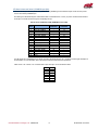
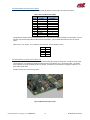
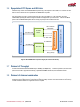
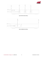
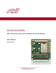
WLAN25203ER WLAN35203ER Mini-PCI Express Card Carrier with Wi-Fi Module User’s Manual BDM-610020110 Rev. C RTD Embedded Technologies, Inc. AS9100 and ISO 9001 Certified RTD Embedded Technologies, Inc. 103 Innovation Boulevard State College, PA 16803 USA Telephone: 814-234-8087 Fax: 814-234-5218 www.rtd.com [email protected] [email protected] Revision History Rev A Rev B Rev C Initial Release, derived from BDM-610020089 rev C (WLAN25202) Added 6th antenna pair Added W_DISABLE# inputs for each socket to I/O connector CN4 Added WAKE# signal support for each socket and true +3.3V auxiliary power Update power figures to reflect latest version of PCB Updated physical dimensions drawing Improved organization of section 3.3.1 (external I/O connectors) List recommended antenna and adapter cable kit, XK-CM111 Removed mention of Half-Mini card standoffs Complete overhaul of manual; restructured and reworded for improved clarity Added table of I/O connectors and improved bus connector table to shows function, size & pitch, and mating connectors Added pinouts for the Mini PCI Express socket connectors Added image of bottom-side of board to show SIM card socket Added description of LED current limiting resistors Added a diagram to explain lane repopulation Added link to PCI Express Mini Card specification Added IDAN external I/O pinouts Improve pinout tables to indicate pin connection to Mini PCI Express sockets Improve antennae connector table to indicate which connectors are spares Correct designator for PCI bus connector as needed Advanced Analog I/O, Advanced Digital I/O, aAIO, aDIO, a2DIO, Autonomous SmartCal, “Catch the Express”, cpuModule, dspFramework, dspModule, expressMate, ExpressPlatform, HiDANplus, “MIL Value for COTS prices”, multiPort, PlatformBus, and PC/104EZ are trademarks, and “Accessing the Analog World”, dataModule, IDAN, HiDAN, RTD, and the RTD logo are registered trademarks of RTD Embedded Technologies, Inc (formerly Real Time Devices, Inc.). PS/2 is a trademark of International Business Machines Inc. PCI, PCI Express, and PCIe are trademarks of PCI-SIG. PC/104, PC/104-Plus, PCI-104, PCIe/104, PCI/104-Express and 104 are trademarks of the PC/104 Embedded Consortium. All other trademarks appearing in this document are the property of their respective owners. Failure to follow the instructions found in this manual may result in damage to the product described in this manual, or other components of the system. The procedure set forth in this manual shall only be performed by persons qualified to service electronic equipment. Contents and specifications within this manual are given without warranty, and are subject to change without notice. RTD Embedded Technologies, Inc. shall not be liable for errors or omissions in this manual, or for any loss, damage, or injury in connection with the use of this manual. Copyright © 2015 by RTD Embedded Technologies, Inc. All rights reserved. RTD Embedded Technologies, Inc. | www.rtd.com iii WLAN25203ER User’s Manual Table of Contents 1 2 3 4 Introduction 6 1.1 Product Overview........................................................................................................................................................................ 6 1.2 Board Features ........................................................................................................................................................................... 6 1.3 Ordering Information ................................................................................................................................................................... 7 1.3.1 Recommended Antenna and Adapter Cable 7 1.4 Contact Information .................................................................................................................................................................... 7 1.4.1 Sales Support 7 1.4.2 Technical Support 7 Specifications 8 2.1 Board Operating Conditions ....................................................................................................................................................... 8 2.2 Board Electrical Characteristics .................................................................................................................................................. 8 2.3 PCI Express Mini Card Operating Conditions ............................................................................................................................ 8 2.4 Physical Characteristics .............................................................................................................................................................. 9 Board Connections and Functionality 10 3.1 Board Handling Precautions ..................................................................................................................................................... 10 3.2 Steps for Installing .................................................................................................................................................................... 10 3.3 Connector and Jumper Locations ............................................................................................................................................. 11 3.4 Functional Diagram ................................................................................................................................................................... 12 3.5 Connector and Jumper Functionality ........................................................................................................................................ 12 3.5.1 Bus Connectors 12 PCIe Connectors (CN1 – Top, CN2 – Bottom) 12 PCI Connector (CN3) - WLAN25203ER only 12 3.5.2 Internal and External I/O Connectors 13 Mini PCI Express Sockets A and B (CN6, CN7) 14 MCX Connectors (CN5, CN9, CN10, CN11, CN13, CN15) 14 LED Status Indicators and Socket W_DISABLE# Inputs (CN4) 15 User Identity Module connection for Slot A (CN20) 16 User Identity Module connection for Slot B (CN21, U5) 16 3.6 Repopulation of PCI Express and USB Links ........................................................................................................................... 17 3.7 Wireless LAN Throughput ......................................................................................................................................................... 17 3.8 Wireless LAN Antenna Considerations..................................................................................................................................... 17 IDAN Connections 18 4.1 Module Handling Precautions ................................................................................................................................................... 18 4.2 Physical Characteristics ............................................................................................................................................................ 18 4.3 External I/O Connectors ........................................................................................................................................................... 20 4.3.1.1 Reverse Polarity SMA (RP-SMA) Antennae Connectors 20 4.3.1.2 LED Status Indicators and Socket W_DISABLE# Inputs 20 4.4 Steps for Installing .................................................................................................................................................................... 21 5 Troubleshooting 22 6 Additional Information 23 7 6.1 PC/104 Specifications ............................................................................................................................................................... 23 6.2 PCI and PCI Express Specification .......................................................................................................................................... 23 6.3 PCI Express Mini Card Electromechanical Specification ......................................................................................................... 23 Limited Warranty RTD Embedded Technologies, Inc. | www.rtd.com 24 iv WLAN25203ER User’s Manual Table of Figures Figure 1: Board Dimensions ..................................................................................................................................................................................... 9 Figure 2: Example 104™Stack ............................................................................................................................................................................... 10 Figure 3: Board Connections .................................................................................................................................................................................. 11 Figure 4: WLAN25203ER Block Diagram ............................................................................................................................................................... 12 Figure 5: SIM Card Socket (U5) for Slot B.............................................................................................................................................................. 16 Figure 6: WLAN25203ER Link Repopulation Diagram (I/O Connectors Not Shown) ............................................................................................ 17 Figure 7: IDAN Dimensions – L x W x H................................................................................................................................................................. 18 Figure 8: IDAN Front Panel Drawing ...................................................................................................................................................................... 19 Figure 9: IDAN Back Panel Drawing....................................................................................................................................................................... 19 Figure 10: Example IDAN System .......................................................................................................................................................................... 21 Table of Tables Table 1: Ordering Options ........................................................................................................................................................................................ 7 Table 2: Recommended Cable Kit ............................................................................................................................................................................ 7 Table 3: Operating Environment and Storage Conditions ........................................................................................................................................ 8 Table 4: Supply Voltage Requirements .................................................................................................................................................................... 8 Table 5: Power Ratings ............................................................................................................................................................................................ 8 Table 6: WLAN25203ER Bus Connectors .............................................................................................................................................................. 12 Table 7: WLAN25203ER I/O Connectors ............................................................................................................................................................... 13 Table 8: CN6 and CN7 Pin Assignments................................................................................................................................................................ 14 Table 9: MCX to U.FL Connector Mapping............................................................................................................................................................. 14 Table 10: Pinout of LED Status and W_DISABLE# Connector (CN4) ................................................................................................................... 15 Table 11: Pinout of UIM Connector (CN20) ............................................................................................................................................................ 16 Table 12: IDAN Pinout of LED Status and W_DISABLE# Connector (CN4) .......................................................................................................... 20 RTD Embedded Technologies, Inc. | www.rtd.com v WLAN25203ER User’s Manual 1 Introduction 1.1 Product Overview RTD’s WLAN25203ER and WLAN35203ER modules offer dual Mini PCI Express sockets, designed to permit integration of third party Mini PCI Express modules into rugged PCIe/104 and PCI/104-Express systems and enclosures. Mini PCI Express (also referred to as PCI Express Mini Card, Mini PCIe, mPCIe, and PEM) is a form factor for devices which supports both PCI Express and USB 2.0 connectivity. An onboard PCIe Gen 2 switch provides a x1 PCI Express connection to each of the dual sockets on the WLAN25203ER and WLAN35203ER, using only one upstream x1 PCI Express link from the bus. Similarly, an onboard USB 2.0 hub generates a USB 2.0 link for each of the dual sockets using only one USB 2.0 link from the bus. Additional links on the PCIe Gen2 switch and USB 2.0 hub are utilized to repopulate the x1 PCI Express link and USB link these devices use from the host, making these links available to the next x1 PCI Express or USB peripheral in the system. For devices installed in the dual mini PCI Express sockets of the WLAN25203ER or WLAN35203ER-- referred to as Sockets A and B throughout this hardware manual (or designators CN6 and CN7, respectively) – a set of three U.FL antennae connectors are available per socket, permitting easy wiring and breakout to a corresponding set of MCX antennae connectors on the board edge. The dual sockets on the WLAN25203ER and WLAN35203ER permit mounting of full and half-length Mini PCI Express modules, allowing maximum flexibility with the specification. A full-size Wireless Mini PCI Express controller card based on the Atheros AR9280 chipset is installed in the first Mini PCI Express socket on the WLAN25203ER and WLAN35203ER. This wireless Ethernet controller module utilizes three pairs of the onboard U.FL and MCX antennae connectors. The second Mini PCI Express socket and an additional three pairs of U.FL and MCX antennae connectors are available for the user. NOTE: The WLAN25203ER is a PCI/104-Express module, and includes a pass-through PCI connector. The WLAN35203ER is PCIe/104, and does not include a pass-through PCI connector. Throughout the remainder of this manual, “WLAN25203ER” refers to both boards unless otherwise noted. 1.2 Board Features PCI Express Universal Connector o Permits compatibility with PCIe/104 Type 1 and Type 2 cpuModules o CPU_DIR pin permits stacking above or below the CPU o +5V-only operation Pass-through PCI Connector (WLAN25203ER only) Onboard PCIe Gen 2 Switch and USB 2.0 hub o Dual sockets require only one x1 PCI Express link and/or one USB 2.0 link for operation o Full x1 PCI Express link and USB 2.0 link repopulation Dual Mini PCI Express Card Sockets o Each socket supports three modes of operation Single x1 PCIe link and single USB 2.0 link Single x1 PCIe link Single USB 2.0 link o Mounting holes permit installation of Full-Mini and Half-Mini sized Mini PCI Express modules o I/O connector provides external access to W_DISABLE# input and LED status outputs on both Mini PCI Express sockets o 6 external antennae connectors for use with Wi-Fi/GPS/GSM cards (3 available) o WAKE# signal support for each socket o UIM / SIM card connections for each Mini PCI Express card slot RTD Embedded Technologies, Inc. | www.rtd.com 6 WLAN25203ER User’s Manual Atheros AR9590 WLAN Mini PCI-Express Card o Compliant to IEEE Standards: 802.11a/b/g/n o Support for 3x3 MIMO with spatial multiplexing o Supports up to 450Mbps physical data rates o Dual-band 2.4GHz and 5GHz with 20/40MHz channel width o Supports 802.11x authentication, 64/128/152Bit WEP, IEEE802.11i encryption o Multi-Country Roaming Supported (IEEE802.11d Global Harmonization Standard) o Compliant with PCI-Express Mini Card 1.1 Standard o Drivers provided for Windows XP and Windows 7 (32-bit and 64-bit) o Natively supported in Linux via open source ath9k driver (kernel 3.2.0 or later) 1.3 Ordering Information The WLAN25203ER and WLAN35203ER are available with the following options: Table 1: Ordering Options Part Number WLAN25203ER WLAN35203ER IDAN-WLAN25203ER IDAN-WLAN35203ER Description PCI/104-Express Mini PCI-E Card add-on board w/ Atheros WLAN module installed PCIe/104Mini PCI-E Card add-on board w/ Atheros WLAN module installed PCI/104-Express Mini PCI-E Card add-on board in IDAN enclosure w/ Atheros module installed PCIe/104Mini PCI-E Card add-on board in IDAN enclosure w/ Atheros module installed The Intelligent Data Acquisition Node (IDAN™) building block can be used in just about any combination with other IDAN building blocks to create a simple but rugged 104™ stack. For more information, see IDAN Connections on page 18. This module can also be incorporated in a custom-built RTD HiDAN™ or HiDANplus High Reliability Intelligent Data Acquisition Node. Contact RTD sales for more information on our high reliability systems. 1.3.1 RECOMMENDED ANTENNA AND ADAPTER CABLE An antenna and extension cable kit is offered for the WLAN25203ER and WLAN35203ER. The cable kit includes one 2.5/5 GHz antenna with 50-ohm RP-SMA connector and an extension cable to adapt from the RP-SMA connector on the antenna to the MCX cables on the WLAN25203 and WLAN35203ER. A quantity of three cable kits is recommended for use with the WLAN25203ER and WLAN35203ER. Table 2: Recommended Cable Kit Part Number XK-CM111 Description One 2.5/5 GHz antenna and one adapter cable for use with the WLAN25203ER and WLAN35203ER 1.4 Contact Information 1.4.1 SALES SUPPORT For sales inquiries, you can contact RTD Embedded Technologies sales via the following methods: Phone: E-Mail: 1.4.2 1-814-234-8087 [email protected] Monday through Friday, 8:00am to 5:00pm (EST). TECHNICAL SUPPORT If you are having problems with you system, please try the steps in the Troubleshooting section of this manual. For help with this product, or any other product made by RTD, you can contact RTD Embedded Technologies technical support via the following methods: Phone: E-Mail: 1-814-234-8087 Monday through Friday, 8:00am to 5:00pm (EST). [email protected] RTD Embedded Technologies, Inc. | www.rtd.com 7 WLAN25203ER User’s Manual 2 Specifications 2.1 Board Operating Conditions Table 3: Operating Environment and Storage Conditions Symbol Ta Ts RH Parameter Operating Temperature Storage Temperature Relative Humidity Test Condition Min -40 -55 0 Non-Condensing Max +85 +125 90% Unit C C % NOTE: The Operating Environment and Storage Conditions listed in Table 3 apply to the WLAN25203ER and WLAN35203ER boards only. For recommended operating conditions of third party Mini PCI Express modules, refer to documentation from the manufacturer. 2.2 Board Electrical Characteristics The bus connectors on the WLAN25203ER and WLAN35203ER offer several voltage inputs. Only +5V is required for operation, and is used to generate the voltage requirements for both Mini PCI Express sockets. All other bus connector supply voltages are pass-through and unused by the WLAN25203ER and WLAN35203ER. Table 4: Supply Voltage Requirements Symbol Vcc5 Vcc5-STBY Vcc3 Vcc12 Vcc-12 Parameter 5 V Supply Voltage 5 V Stand-by Supply Voltage 3.3 V Supply Voltage 12 V Supply Voltage -12 V Supply Voltage Note WLAN25203ER only Min 4.75 n/a n/a n/a n/a Max 5.25 n/a n/a n/a n/a Unit V V V V V Max 2.65 530 Unit W mA Supply current and power consumption for the WLAN25203ER and WLAN35203ER are listed in the table below. Table 5: Power Ratings Symbol P Icc5 Icc3.3-AB-PK Icc1.5-AB-PK Icc3.3 Icc1.5 Parameter Test Condition Min Power Consumption Vcc5 = 5.0 V, Typical 5 V Input Supply Current Active Mini PCI Express – Peak Current per Socket 3.3 V Input Supply Current Peak current; Socket A or B 1.5 V Input Supply Current Peak current; Socket A or B Mini PCI Express – Combined Current (Sockets A and B) 3.3 V Input Supply Current Combined current; Socket A + B 1.5 V Input Supply Current Combined current; Socket A + B 2.750 0.500 A A 4.000 1.000 A A 2.3 PCI Express Mini Card Operating Conditions Each Mini PCI Express module has its own individual operating conditions which will vary from one manufacturer’s device to another. Installing third party Mini PCI Express modules on the WLAN25203ER can affect the overall operating temperature of the system. Make sure to verify the operating conditions of third party Mini PCI Express modules before using the WLAN25203ER in extreme conditions. RTD Embedded Technologies, Inc. | www.rtd.com 8 WLAN25203ER User’s Manual 2.4 Physical Characteristics Weight: Approximately 55 g (0.12 lbs.) Dimensions: 90.17 mm L x 95.89 mm W (3.550 in L x 3.775 in W) Figure 1: Board Dimensions RTD Embedded Technologies, Inc. | www.rtd.com 9 WLAN25203ER User’s Manual 3 Board Connections and Functionality 3.1 Board Handling Precautions To prevent damage due to Electrostatic Discharge (ESD), keep your board in its antistatic bag until you are ready to install it into your system. When removing it from the bag, hold the board at the edges, and do not touch the components or connectors. Handle the board in an antistatic environment, and use a grounded workbench for testing and handling of your hardware. 3.2 Steps for Installing 1. 2. 3. 4. 5. 6. 7. 8. 9. 10. 11. 12. Always work at an ESD protected workstation, and wear a grounded wrist-strap. Turn off power to the PC/104 system or stack. Select and install stand-offs to properly position the module on the stack. Remove the module from its anti-static bag. Check that pins of the bus connector are properly positioned. Check the stacking order; make sure all of the busses used by the peripheral cards are connected to the cpuModule. Hold the module by its edges and orient it so the bus connector pins line up with the matching connector on the stack. Gently and evenly press the module onto the PC/104 stack. If any boards are to be stacked above this module, install them. Attach any necessary cables to the PC/104 stack. Re-connect the power cord and apply power to the stack. Boot the system and verify that all of the hardware is working properly. Figure 2: Example 104™Stack RTD Embedded Technologies, Inc. | www.rtd.com 10 WLAN25203ER User’s Manual 3.3 Connector and Jumper Locations The tables in this section list designator callouts for the various functions of the bus connectors, I/O connectors, and jumpers found on the WLAN25203ER and WLAN35203ER. Also included are the size and pitch of each connector as well as mating connector information. The following top-side photo provides a reference for designators and their locations. PCI Connector (CN3) (CN5) Status LEDs, W_DISABLE# Inputs (CN4) Spare Connectors (CN11) (CN13) External MCX Antennae Connectors (CN15) UIM / SIM Card Connectors (CN20, CN21) (CN9) Spare Connector (CN5) Slot B (CN7) Slot A (CN6) PCIe Connector (CN1, CN2) Figure 3: Board Connections RTD Embedded Technologies, Inc. | www.rtd.com 11 WLAN25203ER User’s Manual 3.4 Functional Diagram PCIe x1 Link PCIe Mux/ Demux PCIe Packet Switch PCIe Bus PCIe Mux/ Demux 2 PCIe x1 Links Slot A Atheros Wi-Fi Card The Figure below shows the functional block diagram of the WLAN25203ER. 1 USB Link USB Signal Switch USB 1 USB Link Hub 2 USB Links Slot B Available for User PCIe x1 Link UIM Signals (CN20) LED Signals (CN4) SIM Card U5 (CN21 optional) Figure 4: WLAN25203ER Block Diagram 3.5 Connector and Jumper Functionality 3.5.1 BUS CONNECTORS Table 6: WLAN25203ER Bus Connectors Connector CN1 CN2 CN3 Function PCIe/104 Universal Bus (Top) PCIe/104 Universal Bus (Bottom) PCI-104 (PCI) Bus (WLAN25203ER only) Size and Pitch 156-pin, 0.635mm 156-pin, 0.635mm 120-pin, 2mm Mating Connector Samtec ASP-129646-03 Samtec ASP-129637-03 Samtec ESQT-130-02-G-Q-368 PCIe Connectors (CN1 – Top, CN2 – Bottom) The WLAN25203ER is a “Universal” board, and can connect to either a Type 1 or Type 2 connector of a PCIe/104 or PCI-104 Express system. The position and pin assignments are compliant with the PCI/104-Express Specification. (See PC/104 Specifications on page 23) PCI Connector (CN3) - WLAN25203ER only The PCI connector is the connection to PCI peripheral modules. This connector is used on this board as a pass through connector only. RTD Embedded Technologies, Inc. | www.rtd.com 12 WLAN25203ER User’s Manual 3.5.2 INTERNAL AND EXTERNAL I/O CONNECTORS The WlAN25203ER offers two sockets for installing a third party Mini PCI Express module, Socket A (CN6) and Socket B (CN7). For each socket, three onboard U.FL antennae connectors are offered to easily bring out any connections from the installed module to the WLAN25203ER, allowing the user to easily interface to these connections using a rugged MCX connector. A full-size Wireless Mini PCI Express controller card based on the Atheros AR9280 chipset is installed in the first Mini PCI Express socket on the WLAN25203ER and WLAN35203ER (Socket A, or CN6). This wireless Ethernet controller module utilizes three pairs of the onboard U.FL and MCX antennae connectors. The second Mini PCI Express socket (Socket B, or CN7) and an additional three pairs of U.FL and MCX antennae connectors are available for the user. Several additional external I/O connectors allow external interfacing to auxiliary signaling on the Mini PCI Express sockets connectors. Table 7: WLAN25203ER I/O Connectors Socket A CN6 CN20 Socket B CN7 CN21, U5 Socket A / B CN4 CN8, CN16, CN17, CN22, CN23, CN24 CN5, CN9, CN10, CN11, CN13, CN15 Function Mini PCI Express, Socket A Socket A: UIM / SIM connection Function Mini PCI Express, Socket B Socket B: UIM / SIM connection Function Socket A & Socket B LED signals Socket A & Socket B U.FL connector receptacle Size and Pitch Mating Connector (Refer to PCI Express Mini Card Electromechanical Specification) 2x5, 0.1”, right angle 3M 89110-0001 Size and Pitch Mating Connector (Refer to PCI Express Mini Card Electromechanical Specification) 2x5, 0.1”, right angle 3M 89110-0001 Size and Pitch Mating Connector 2x6, 0.1”, right angle AMP 87456-8 Hirose Connectors, U.FL-R(Various; refer to Hirose SMT Connectors product datasheet) Socket A & Socket B MCX 50-ohm straight jack receptacle Johnson Components, 1333701-211 RTD Embedded Technologies, Inc. | www.rtd.com 13 (Various) WLAN25203ER User’s Manual Mini PCI Express Sockets A and B (CN6, CN7) The WLAN25203ER offers two soldered-down connectors that support third party Mini PCI Express modules. Sockets A and B on the WLAN25203ER (or designators CN3 and CN4) each offer one downstream x1 PCI Express Gen 2 link and one downstream USB 2.0 link from the host cpuModule to the Mini PCI Express device installed in the socket. For maximum flexibility, the WLAN25203ER provides mounting holes for cards designed to both the Full-Mini and Half-Mini card Mini PCI Express form factors. The pinout for each Mini PCI Express connector is shown below. Table 8: CN6 and CN7 Pin Assignments Pin Name (Reserved) (Reserved) (Reserved) (Reserved) GND 3.3 V 3.3 V GND GND PET0_P PET0_N GND GND PER0_P PER0_N GND (Reserved) (Reserved) Pin Name GND REFCLK_P REFCLK_N GND CLKREQ# (Not Connected) (Not Connected) WAKE# # 51 49 47 45 43 41 39 37 35 33 31 29 27 25 23 21 19 17 # 15 13 11 9 7 5 3 1 # 52 50 48 46 44 42 40 38 36 34 32 30 28 26 24 22 20 18 # 16 14 12 10 8 6 4 2 Pin Name 3.3 V GND 1.5 V LED_WPAN# LED_WLAN# LED_WWAN# GND USB_D_P USB_D_N GND SMB_DATA SMB_CLK 1.5 V GND 3.3 V PERST# W_DISABLE# GND Pin Name UIM_VPP UIM_RESET UIM_CLK UIM_DATA UIM_PWR 1.5 V GND 3.3 V MCX Connectors (CN5, CN9, CN10, CN11, CN13, CN15) The MCX connectors allow the user to connect external antennas to an installed GSM/GPS/Wi-Fi card. Mini-PCIe wireless cards typically use U.FL connectors, which must be adapted to MCX connectors to interface with common antenna cables. The onboard U.FL connectors facilitate this. The following table shows the mapping relationship between the onboard U.FL connectors and MCX connectors. Table 9: MCX to U.FL Connector Mapping U.FL Connector CN8 CN16 CN17 CN22 CN23 CN24 MCX Connector CN10 CN9 CN11 CN13 CN15 CN5 Function (spare) Antenna (spare) Antenna Antenna (spare) By default, the installed Atheros card will use CN9, CN15, and CN13 antenna connections. RTD Embedded Technologies, Inc. | www.rtd.com 14 WLAN25203ER User’s Manual LED Status Indicators and Socket W_DISABLE# Inputs (CN4) Connector CN4 brings out the LED_WPAN#, LED_WLAN#, and LED_WWAN# signals on the Mini PCI Express sockets and also provides access to the socket W_DISABLE# inputs. Each LED signal on the Mini PCI Express sockets CN6 and CN7 is current limited with a 110 ohm (1%) resistor. Connect the LED cathode to the odd pins, and the LED anode to the signal’s corresponding even pin. Table 10: Pinout of LED Status and W_DISABLE# Connector (CN4) CN4 Pin # 1 2 3 4 5 6 7 8 9 10 11 12 13 14 15 16 Function Slot A (CN6) Pin Number – – – 20 – – – – – – 42 – 44 – 46 – Ground Slot B, W_DISABLE# Ground Slot A, W_DISABLE# Slot B, LED_WWAN# +3.3V Slot B, LED_WLAN# +3.3V Slot B, LED_WPAN# +3.3V Slot A, LED_WWAN# +3.3V Slot A, LED_WLAN# +3.3V Slot A, LED_WPAN# +3.3V Slot B (CN7) Pin Number – 20 – – 42 – 44 – 46 – – – – – – – The LED signals and W_DISABLE# inputs are directly connected to the Mini PCI Express slots. The behavior of these signals will depend on the card installed. For more information, refer to the PCI Express Mini Card Electromechanical specification. CN4 is a 2x8 0.1” DIL connector. Pin 1 is indicated with a square solder pad. Pins are numbered as follows. 16 14 12 10 8 6 4 2 RTD Embedded Technologies, Inc. | www.rtd.com 15 13 11 9 7 5 3 1 15 WLAN25203ER User’s Manual User Identity Module connection for Slot A (CN20) CN20 is the User Identity Module (UIM) signal connection for Mini PCI Express card Slot A (CN6). Pin functions are as follows: Table 11: Pinout of UIM Connector (CN20) CN20 Pin # 1 2 3 4 5 6 7 8 9 10 Slot A Function UIM_RESET GND UIM_DATA GND UIM_CLK GND UIM_VPP GND UIM_PWR GND Slot A (CN6) Pin Number 14 – 10 – 12 – 16 – 8 – The UIM signals are directly connected to the Mini PCI Express slot. The behavior of these signals will depend on the card installed. For more information, refer to the PCI Express Mini Card Electromechanical specification. (The pre-installed Atheros Wi-Fi card does not use these signals.) CN20 is a 2x5 0.1” DIL connector. Pin 1 is indicated a square solder pad. Pins are numbered as follows. 10 8 6 4 2 9 7 5 3 1 User Identity Module connection for Slot B (CN21, U5) The SIM Card socket (U5) on the bottom side of the board provides the UIM signal connection for Slot B (CN7). The SIM card socket accepts a standard SIM card. As an alternative to the SIM card socket, the board may be built with a 2x5 0.1” DIL connector (CN21). The standard board configuration comes with U5 installed and CN21 not populated. Contact RTD if you are interested in changing this configuration. The pinout of CN21 matches CN20. The SIM card socket (U5) is shown in the figure below. Figure 5: SIM Card Socket (U5) for Slot B RTD Embedded Technologies, Inc. | www.rtd.com 16 WLAN25203ER User’s Manual 3.6 Repopulation of PCI Express and USB Links The Mini PCI Express sockets on the WLAN25203ER each operate using a x1 PCI Express link and/or USB 2.0 link. To relieve some of the stress on the system, the WLAN25203ER has an onboard PCI-Express Gen 2 switch and a USB 2.0 hub to generate these links, reducing the number of resources needed from the host cpuModule for the WLAN25203ER to operate. These components are also used to generate one PCI Express Gen 2 link and one USB 2.0 link on the “downstream” side of the WLAN25203ER, repopulating the used links making them available for other peripherals up or down the stack. This allows each Mini PCI Express socket on WLAN25203ER to operate without consuming any PCI Express link or USB link on the bus. PCIe Gen 2 Switch Two x1 PCIe Links Two 1 USB Links One 1 USB Link USB 2.0 Hub “Downstream” PCI Express Bus Connector (CN1 or CN2) One x1 PCIe Link Mini PCIe Card Socket A and B Mini PCIe Card Sockets A and B “Upstream” PCI Express Bus Connector One x1 PCIe Link (Repopulated) One x1 USB Link (Repopulated) Figure 6: WLAN25203ER Link Repopulation Diagram (I/O Connectors Not Shown) 3.7 Wireless LAN Throughput The maximum theoretical bandwidth of the AR9590 chipset is 450Mbps (56.25 MBytes/sec). To achieve this performance, the card must be connected to an access point with similar performance characteristics. Note that per the IEEE 802.11n Specification, a 450Mbps data rate requires the access point to support all of the following: 3x Spatial Streams, 40MHz Channel Width, and a 400ns Guard Interval. 3.8 Wireless LAN Antenna Considerations Since the WLAN25203 supports 3x3 MIMO operation, it is strongly recommended that all three antennas be connected for best performance. A dual-band (2.4GHz and 5GHz) antenna is recommended for maximum versatility. However, in an environment where it is known that only the 2.4GHz or 5GHz band will be used, a single-band antenna is acceptable. RTD Embedded Technologies, Inc. | www.rtd.com 17 WLAN25203ER User’s Manual 4 IDAN Connections 4.1 Module Handling Precautions To prevent damage due to Electrostatic Discharge (ESD), keep your module in its antistatic bag until you are ready to install it into your system. When removing it from the bag, hold the module by the aluminum enclosure, and do not touch the components or connectors. Handle the module in an antistatic environment, and use a grounded workbench for testing and handling of your hardware. 4.2 Physical Characteristics Weight: Approximately 0.21 Kg (0.46 lbs.) Dimensions: 151.972 mm L x 129.978 mm W x 16.993 mm H (5.983 in L x 5.117 in W x 0.669 in H) Figure 7: IDAN Dimensions – L x W x H RTD Embedded Technologies, Inc. | www.rtd.com 18 WLAN25203ER User’s Manual Figure 8: IDAN Front Panel Drawing Figure 9: IDAN Back Panel Drawing RTD Embedded Technologies, Inc. | www.rtd.com 19 WLAN25203ER User’s Manual 4.3 External I/O Connectors 4.3.1.1 REVERSE POLARITY SMA (RP-SMA) ANTENNAE CONNECTORS For improved signal transmission, six reverse polarity SMA (RP-SMA) connectors on the IDAN frame (labeled: 1, 2, 3, 4, 5, 6) allow the user to connect external antennae to GSM, GPS, and/or Wi-Fi Mini PCIe modules installed on the WLAN25203ER and WLAN35203ER. This connection is accomplished via the onboard MCX connectors (CN5, CN9, CN10, CN11, CN13, CN15). For more information on the MCX connectors, see page 14. 4.3.1.2 LED STATUS INDICATORS AND SOCKET W_DISABLE# INPUTS A 15-pin female DSUB connector labeled “I/O” allows access to LED status indicators on the Mini PCI Express cards installed on the WLAN25203ER and WLAN25203ER, and also provides access to the W_DISABLE# input of each socket. For more information on the LED status indicators and socket W_DISABLE# input, see page 15. The pin mapping of the 15-pin DSUB connector to connector CN4 on the WLAN25203ER and WLAN35203ER is shown in the following table: Table 12: IDAN Pinout of LED Status and W_DISABLE# Connector (CN4) 15-pin female DSUB Pin # 1 2 3 4 5 6 7 8 9 10 11 12 13 14 15 -- CN4 Pin # 1 3 5 7 9 11 13 15 2 4 6 8 10 12 14 16 Function Ground Ground Slot B LED_WWAN# Slot B LED_WLAN# Slot B LED_WPAN# Slot A LED_WWAN# Slot A LED_WLAN# Slot A LED_WPAN# Slot B W_DISABLE# Slot A W_DISABLE# +3.3V +3.3V +3.3V +3.3V +3.3V +3.3V The LED signals and W_DISABLE# inputs are directly connected to the Mini PCI Express slots. The behavior of these signals will depend on the card installed. For more information, refer to the PCI Express Mini Card Electromechanical specification. RTD Embedded Technologies, Inc. | www.rtd.com 20 WLAN25203ER User’s Manual 4.4 Steps for Installing 1. 2. 3. 4. 5. 6. 7. 8. 9. 10. 11. 12. Always work at an ESD protected workstation, and wear a grounded wrist-strap. Turn off power to the IDAN system. Remove the module from its anti-static bag. Check that pins of the bus connector are properly positioned. Check the stacking order; make sure all of the busses used by the peripheral cards are connected to the cpuModule. Hold the module by its edges and orient it so the bus connector pins line up with the matching connector on the stack. Gently and evenly press the module onto the IDAN system. If any boards are to be stacked above this module, install them. Finish assembling the IDAN stack by installing screws of an appropriate length. Attach any necessary cables to the IDAN system. Re-connect the power cord and apply power to the stack. Boot the system and verify that all of the hardware is working properly. Figure 10: Example IDAN System RTD Embedded Technologies, Inc. | www.rtd.com 21 WLAN25203ER User’s Manual 5 Troubleshooting If you are having problems with your system, please try the following initial steps: Simplify the System – Remove modules one at a time from your system to see if there is a specific module that is causing a problem. Perform you troubleshooting with the least number of modules in the system possible. Swap Components – Try replacing parts in the system one at a time with similar parts to determine if a part is faulty or if a type of part is configured incorrectly. If problems persist, or you have questions about configuring this product, contact RTD Embedded Technologies via the following methods: Phone: E-Mail: +1-814-234-8087 [email protected] Be sure to check the RTD web site (http://www.rtd.com) frequently for product updates, including newer versions of the board manual and application software. RTD Embedded Technologies, Inc. | www.rtd.com 22 WLAN25203ER User’s Manual 6 Additional Information 6.1 PC/104 Specifications A copy of the latest PC/104 specifications can be found on the webpage for the PC/104 Embedded Consortium: www.pc104.org 6.2 PCI and PCI Express Specification A copy of the latest PCI and PCI Express specifications can be found on the webpage for the PCI Special Interest Group: www.pcisig.com 6.3 PCI Express Mini Card Electromechanical Specification A copy of the latest PCI Express Mini Card Electromechanical Specification can also be found on the webpage for the PCI Special Interest Group: www.pcisig.com RTD Embedded Technologies, Inc. | www.rtd.com 23 WLAN25203ER User’s Manual 7 Limited Warranty RTD Embedded Technologies, Inc. warrants the hardware and software products it manufactures and produces to be free from defects in materials and workmanship for one year following the date of shipment from RTD Embedded Technologies, Inc. This warranty is limited to the original purchaser of product and is not transferable. During the one year warranty period, RTD Embedded Technologies will repair or replace, at its option, any defective products or parts at no additional charge, provided that the product is returned, shipping prepaid, to RTD Embedded Technologies. All replaced parts and products become the property of RTD Embedded Technologies. Before returning any product for repair, customers are required to contact the factory for a Return Material Authorization (RMA) number. This limited warranty does not extend to any products which have been damaged as a result of accident, misuse, abuse (such as: use of incorrect input voltages, improper or insufficient ventilation, failure to follow the operating instructions that are provided by RTD Embedded Technologies, “acts of God” or other contingencies beyond the control of RTD Embedded Technologies), or as a result of service or modification by anyone other than RTD Embedded Technologies. Except as expressly set forth above, no other warranties are expressed or implied, including, but not limited to, any implied warranties of merchantability and fitness for a particular purpose, and RTD Embedded Technologies expressly disclaims all warranties not stated herein. All implied warranties, including implied warranties for merchantability and fitness for a particular purpose, are limited to the duration of this warranty. In the event the product is not free from defects as warranted above, the purchaser's sole remedy shall be repair or replacement as provided above. Under no circumstances will RTD Embedded Technologies be liable to the purchaser or any user for any damages, including any incidental or consequential damages, expenses, lost profits, lost savings, or other damages arising out of the use or inability to use the product. Some states do not allow the exclusion or limitation of incidental or consequential damages for consumer products, and some states do not allow limitations on how long an implied warranty lasts, so the above limitations or exclusions may not apply to you. This warranty gives you specific legal rights, and you may also have other rights which vary from state to state. RTD Embedded Technologies, Inc. | www.rtd.com 24 WLAN25203ER User’s Manual RTD Embedded Technologies, Inc. 103 Innovation Boulevard State College, PA 16803 USA Telephone: 814-234-8087 Fax: 814-234-5218 www.rtd.com [email protected] [email protected] Copyright 2015 by RTD Embedded Technologies, Inc. All rights reserved.