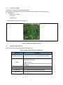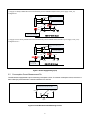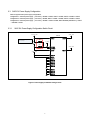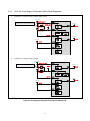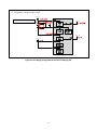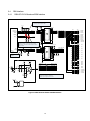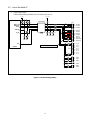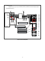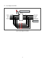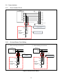
1
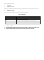
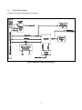
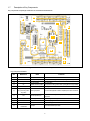
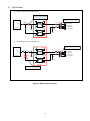
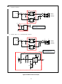
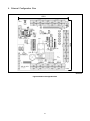
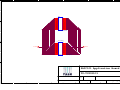
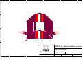
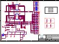
TSA-OP-IC101 User’s Manual Issued:October 20, 2014(Version 1.0) Tessera Technology Corporation TS-TUM02272 Cautionary Notes: ・ ・ ・ ・ ・ ・ ・ ・ ・ The contents of this document are subject to change without notice. This board described in this document is made available for research and development. Reproduction of this document in any format is prohibited without written permission from Tessera Technology Inc. (herein, “ the Company”) The company shall not be liable for any mistakes contained in this document. The company shall not be liable for the infringement of third party patent, copyrights, or other intellectual property rights arising from the use of Tessera Technology products listed in this document. The company does grant any rights concerning Tessera Technology or third party patents, copyrights, or other intellectual property rights based on this material. Circuitry, software or related information included in this document is provided as semiconductor product operation examples and application examples. The user is responsible for the appropriate application of the circuitry, software or related information when designing equipment. The company shall not be liable for loss or damage incurred by the user or other third party based on the use of this circuitry, software or related information. Please handle this product as you would a CMOS device. The user should be particularly careful to protect himself/herself from accumulated static electricity when using this product. Make sure all test and measurement equipment, including the work station, is properly grounded. The user should wear an ESD wrist strap to prevent any buildup of static electricity. Revision History Version Date Ver 1.0 14/10/20 Description Initial version Table of contents 1. 2. Overview..........................................................................................................................................................................................1 1.1 Document Overview .................................................................................................................................................................................1 1.2 Related Terminology.................................................................................................................................................................................1 1.3 RSK Board Features..................................................................................................................................................................................1 1.4 Product Overview......................................................................................................................................................................................2 1.5 Hardware Specifications ...........................................................................................................................................................................2 1.6 Board Block Diagram ...............................................................................................................................................................................3 1.7 Description of Key Components .............................................................................................................................................................4 Function ...........................................................................................................................................................................................5 2.1 Power Supply Switch Setting...................................................................................................................................................................5 2.2 Consumption Current Measurement Pin ................................................................................................................................................6 2.3 SAIC101 Power Supply Configuration..................................................................................................................................................7 2.3.1 SAIC101 Power Supply Configuration Switch Circuit.............................................................................................................7 2.3.2 SAIC101 Power Supply Configuration Switch Circuit Explanation.......................................................................................8 2.4 2.4.1 RSK Interface...........................................................................................................................................................................................10 RSK-OP-IC101 Board and RSK Interface ...............................................................................................................................10 2.5 How to Set Serial I/F ...............................................................................................................................................................................11 2.6 How to Bypass Level Shifter .................................................................................................................................................................13 2.7 MCLK Setting .........................................................................................................................................................................................14 2.8 Sensor Interface........................................................................................................................................................................................16 2.8.1 Sensor Interface Circuit................................................................................................................................................................16 2.8.2 On-board Sensor Circuit Setting.................................................................................................................................................16 2.9 Through-holes ..........................................................................................................................................................................................17 2.9.1 Through-holes for RSK Application Header ............................................................................................................................17 2.9.2 Through-hole (TH1) for External Sensor Board Connection .................................................................................................17 2.9.3 Through-hole (TH2) for Serial Signal Monitoring...................................................................................................................17 2.10 Test Pads ...................................................................................................................................................................................................18 2.11 Jumper Pin/Solder Pin Default Settings................................................................................................................................................18 2.12 Recommended Parts for Non-mounted Connectors ...........................................................................................................................19 3. Bill of Materials ..............................................................................................................................................................................20 4. External Configuration Size.........................................................................................................................................................21 5. Circuit diagram ..............................................................................................................................................................................22 TSA-OP-IC101 User’s Manual 1. Overview 1.1 Document Overview This user’s manual explains the hardware specifications for the Smart Analog IC101 Renesas Starter Kit Option Board. 1.2 Related Terminology This document uses the following terms in explanations of hardware specifications. Table 1-1 Terminology Term SAIC101 RSK SPI UART 1.3 ● ● Definition Abbreviation for Smart Analog IC101 Abbreviation for Renesas Starter Kit Abbreviation for Serial Peripheral Interface communications Abbreviation for Universal Asynchronous Receiver Transmitter RSK Board Features Offers RSK application headers and compatible connectors for evaluating any Renesas MCU used with SAIC101. Comes mounted with temperature sensor (thermistor) for quick and easy operations confirmation. 1 1.4 Product Overview This product is configured with the following components. Some parts are not bundled with the kit and must be purchased and mounted on the board by the user. TSA-OP-IC101 ● ・ RSK-OP-IC101 board ・ Test pins: 6 ・ Read me first The board’s external picture is shown in Figure 1. Figure 1. RSK-OP-IC101 External Picture 1.5 Hardware Specifications Table 1-2 shows the hardware specifications for the RSK board. Table 1-2 Hardware Specifications for RSK Board Spec Item Description Renesas Electronics SAIC101 (RAA730101) Mounted Smart Analog IC 16-bit A/D ΔΣconverter IC with programmable gain amplifier External power-supply connection I/F CPU board connection I/F Interface External sensor I/F Pattern (oscillator/BNC) for MCLK (SAIC101) external input circuit Sampling I/F Supply Voltage Display Mounted sensor Dimensions +5.0V/+3.3V (from CPU board or external power supply LED (Power) Temperature sensor NXFT15XH103FA2 (Murata) Board dimensions 100 x 105mm (W x D) 2 1.6 Board Block Diagram External Power The RSK-OP-IC10 board block diagram is shown below. Power_LED LED On Board Sensor (NXFT15XH103FA2) RSK_Serial_I/F RSK_IO_I/F SAIC101 MCLK External MCLK Input Logic BNC IO_VDD RSK Application header(JA1/2/4/5/6) 3.3V Power select logic AREG_VDD 5.0V External observation i/f SAIC101_VDD Power select oscillator SAIC101_VDD Figure 2. RSK-OP-IC101 Board Block Diagram 3 External Sensor i/f 1.7 Description of Key Components Key components comprising the RSK-OP-101 board are described below. ⑥ ⑦ ⑤ ⑩ ⑥ ⑤ ⑨ ④ ① ⑪ ② ③ ⑥ ⑤ ⑧ Figure 3. RSK-OP-IC101 Board Component Names Key Component Positions No Reference ① JP10, JP11, JP12 ② ③ Parts Function Jumper For on-board sensor connection - BCN expansion pattern Component mounting positions when inputting MCLK through BNC - Universal pattern General pattern ④ U5 Oscillator extension pattern ⑤ JA1/JA2/JA4/JA5/JA6 RSK connection pattern RSK application header connection RSK signal pattern For other RSK application header compatible option board connections Component mounting positions when inputting MCLK through oscillator JA1_COPY/JA2_COPY ⑥ JA4_COPY/JA5_COPY JA6_COPY ⑦ Used for Smart Analog IC analog input, power supply pin and sensor TH1 Sensor expansion pin ⑧ TH2 Serial signal monitor pin For serial signal monitoring ⑨ U2, U3 Level shifter Power supply signal conversion ⑩ JP1 Jumper For power supply 5V/3.3V switch Jumper For serial send/receive pin switch ⑪ JP4/JP5/JP6 JP7/JP8/JP9 expansion. 4 2. Function 2.1 Power Supply Switch Setting Various power sources can be used to power the RSK board, as shown below. ① Supply 5V (CON_5V) from RSK to RSK-OP-IC101 board (default state): Configuration 1 Ap plic atio n hea der JP1: 1-2 short RSK _VDD 1 2 (J A 1) 3 JP1 HJ1 HJ2 RS K_GND EX _VDD SAIC10 1_ VD D CN1 DC GND 0Ω DGN D EX_GND AGND RSK-OP-IC101 Board ② Supply 3.3V (CON_3V3) from RSK to RSK-OP-IC101 board: Configuration 3 Ap plic atio n hea der JP1: 2-3 short RSK_VDD 1 2 (J A 1) 3 JP1 HJ1 HJ2 RS K_ GND EX _VDD SAIC10 1_ VD D CN1 DC GND 0Ω EX_ GND DGN D AGND RSK-OP-IC101 Board ③ Supply 5V/3.3V from RSK-OP-IC101 board to RSK side: Configuration 1 or 3 JP1: 1-2 short RSK_VDD Ap plic atio n hea der 1 2 (J A 1) 3 JP1 HJ1 CN1 5.0V/3.3V RS K_GND EX _VDD SAIC10 1_ VD D DC (V) GND(G) 0Ω EX _GND Supply 5V/3.3 from external power supply input TH HJ2 DGN D AGND RSK-OP-IC101 Board Figure 4. Power Supply Settings (1/2) 5 ④ Supply 5V directly to RSK-OP-IC101 board and isolate power from RSK board(when MCU power supply =CON_5V): Configuration 1 Ap plic atio n hea der JP1: 1-2 short *Select as level shifter power supply RSK_VDD 1 2 (J A 1) 3 Cut solder jumper JP1 HJ1 CN1 5.0V HJ2 RS K_GND EX__VDD SAIC10 1_VD D DC(V) GND(G) 0Ω EX _GND Supply 5V from external power supply input TH DGN D AGND RSK-OP-IC101 Board ⑤ Supply 5V/3/3V directly to RSK-OP-IC101 board and isolate power from RSK board (when MCU power supply =CON_3V3): Configuration 2 or 3 Ap plic atio n hea der JP1: 2-3 short *Select as level shifter power supply RSK_VDD 1 2 (J A 1) 3 Cut solder jumper JP1 HJ1 CN1 RS K_GND EX__VDD SAIC10 1_VD D 5.0V/3.3V DC(V) GND(G) 0Ω EX _GND Supply 5V/3.3 from external power supply input TH HJ2 DGN D AGND RSK-OP-IC101 Board Figure 5. Power Supply Settings (2/2) 2.2 Consumption Current Measurement Pin The RSK board is equipped with a pin for measuring consumption current. To measure consumption current, remove the 0 Ohm resister (R1) and measure the current flow between TP1 and TP2. Remove the 0 Ohm resister (R1) and measure the current flow between TP1 and TP2. RSK _VDD SAIC101_VDD TP1 TP2 A R1 Open Figure 6. Circuit Structure when Measuring Current 6 2.3 SAIC101 Power Supply Configuration SAIC01 supports three power supply configurations. Configuration 1: external power supply (3.3V-5.5V) = RVDD = IOVDD, AREG = AVDD, CREG = ADVDD = DVDD Configuration 2: external power supply (3.3V-5.5V) = RVDD, AREG = AVDD = IOVDD, CREG = ADVDD = DVDD Configuration 2: external power supply (2.7V-3.6V) = RVDD = AVDD= IOVDD, AREG disabled (AREGPD=1), CREG = ADVDD = DVDD 2.3.1 SAIC101 Power Supply Configuration Switch Circuit SAIC101_VDD AREG _ VDD SAIC101 RVDD AREG JP2 Power supply configuration swit ch jum per IO_ VDD AREG _ VDD JP3 IOVDD1 IOVDD2 CREG _VDD AVDD CREG CREG _ VDD ADVDD DVDD AGND1 AGND2 AGND3 AGND4 AGND5 AGND6 AG ND DGND DGND1 DGND2 DGND3 DGND4 U1 Figure 7. Power supply constitution change circuit 7 2.3.2 ① SAIC101 Power Supply Configuration Switch Circuit Explanation Configuration 1: settings and supply voltages (default setting) SAIC10 1_VDD 3. 3 V~5. 5 V Configuration 1: JP2 = short, JP3 = open JP2 3. 3 V~5. 5 V IO__VDD AREG _ VDD SAIC101 RVDD JP3 AREG_ VDD AREG 3.0V LDO 3.0 V IOVD D FLASH 3.0 V In/Output Logic AV DD CR EG_ VDD 2.1V LDO CR EG _VDD 2.1 V CREG 2.1 V AD VDD 16bitΔ ∑ADC DV DD Digital Logic ② Configuration 2: settings and supply voltages SAIC10 1_VDD 3. 3 V~5. 5 V Configuration 2: JP2 = open, JP3 = short JP2 RVDD AREG _ VDD 3.0 V 3.0 V LDO IO_ VDD AREG_VDD JP 3 SAIC101 AREG 3.0 V IOVD D FLASH 3.0 V In/Output Logic AV DD CR EG_VDD 2.1 V LDO CR EG_VDD 2.1 V AD VDD DV DD 16bitΔ ∑ADC Digital 回路 Figure 8. Power Supply Configuration Switch Circuit Settings (1/2) 8 CREG 2.1 V ③ Configuration 3: settings and supply voltages SAIC10 1_VDD 2.7V~3.6V Configuration 3: JP2 = short, JP3 = short JP2 RVD D AREG _ VDD 2.7V~3.6V 3.0 V LDO IO _VDD AREG_VDD JP3 SAIC101 Hiz AREG 2.7V~3.6V IOVD D FLASH 2.7V~3.6V In/Output Logic AV DD CR EG _ VDD 2.1 V LDO CR EG_VDD 2.1 V CREG AD VDD DV DD 16bitΔ ∑ADC Digital 回路 Figure 9. Power Supply Configuration Switch Circuit Settings (2/2) 9 2.1 V 2.4 RSK Interface 2.4.1 RSK-OP-IC101 Board and RSK Interface SMODE pin is pulled down by default; to pull up, solder jumper JH6. IO _VDD IO _VDD RSK_VDD HJ48 10k 10k 10k RSK_VDD HJ49 10k MISO_TX MOSI_RX SCLK MISO_TX MOSI_RX SCLK MISO_TX 100k INT MCLK_OUT 100k HJ6 HJ3 SMODE 100k 100k CS_B CS_B 100k 100k HJ5 100k 100k 100k DGND DGND CS_B pin is pulled down and isolated from MCU by default; to pull up solder jumper HJ3) and to connect to MCU output, solder jumper HJ5. TP 3 SAIC101 INT MCLK MCLK INT MCLK_OUT MCLK_IN 0 50 U1 100k DGND MISO_TX_RSK INT_RSK MOSI_RX_RSK MCLK_OUT_RSK SCLK_RSK CS_B_RSK INT_RSK MCLK_IN_RSK MCLK_OUT_RSK 100k DGND VCCB VCCA G DIR B0 A0 B1 A1 B2 A2 B3 A3 B4 A4 B5 A5 B6 A6 B7 A7 B8 A8 GND GND HD151015T 10k MOSI_RX_RSK SCLK_RSK CS_B_RSK MCLK_IN_RSK 100k 100k 100k 100k 100k 100k 100k DGND DGND DGND 100k U3 HJ45 IO_VDD SA IC101_VDD DGND HJ47 TH2 BNC1 DNF DNF MISO_TX HJ46 TH14 DNF U4 DNF VIN+ TH10 DNF VINDNF TH1 TH9 DGND MCLK DGND DNF TH3 TH5 MOSI_RX SCLK CS_B INT MCLK_OUT MCLK_IN TH7 TH9 TH10 TH11 TH8 TH12 TH13 MISO_TX_RSK MOSI_RX_RSK SCLK_RSK CS_B_RSK INT_RSK MCLK_OUT_RSK MCLK_IN_RSK HA1631S01 DNF DNF DGND DGND TH16 DNF TH18 DNF DGND DNG display part s and JA1/JA2/JA5/JA6 are not mounted on board at shipment. Mount required parts as needed. DGND SA IC101_VDD HJ44 TH4 50 50 JP4 JA2 JP5 50 50 50 50 50 HJ15 JP6 JP7 HJ16 JP8 JP9 HJ17 HJ4 HJ51 HJ18 RSK _VDD RSK_VDD RSK_VDD HJ50 MOSI_RX SCLK CS_B MCLK_IN 100k MISO_TX_RSK DNF U5 DNF DGND Figure 10. RSK-OP-IC101 Board and RSK Interface 10 8 6 10 SCIaRX SCIaTX SCIaCK 7 8 10 12 9 11 6 5 SCIbRX SCIbTX SCIbCK SCIcRX SCIcTX SCIcCK RX232RX RX232TX JA6 U2 DGND HJ14 Test pin for MCLK monitor VCCB VCCA G DIR B0 A0 B1 A1 B2 A2 B3 A3 A4 B4 A5 B5 A6 B6 A7 B7 B8 A8 GND GND HD 151015T JA1 HJ19 HJ20 HJ21 HJ22 HJ23 HJ24 HJ25 HJ26 HJ27 HJ28 HJ29 HJ30 HJ31 HJ32 HJ33 HJ34 HJ35 HJ36 JA2 HJ37 JA1 HJ38 HJ39 JA5 HJ40 HJ41 HJ42 HJ43 JA2 15 IO_0 16 IO_1 17 IO_2 18 IO_3 19 IO_4 20 IO_5 21 IO_6 22 IO_7 7 9 23 IRQ0 IRQ1 IRQ2 23 IRQ3 9 10 IRQ4 IRQ5 19 20 21 22 TimerOut1 TimerOut2 TimerIn1 TimerIN2 2.5 How to Set Serial I/F ① UART Setting Example *When using serial pins SCIcRX (JA6:12) and SCIcTX (JA6:9) IO_VDD 10k RSK_ VDD 10 k 10 k 10 k Level Shifter 10 k JA2 JP4 MISO_TX MOSI_RX SCLK 8 SCIaRX 6 SCIaTX 10 SCIaCK JP5 HJ15 HJ6 JA6 JP6 SMODE 7 8 10 12 9 11 6 5 JP7 HJ3 U2/U3 CS_B 100 k 100k 100k HJ16 JP8 HJ5 DGND DGND DGND JP9 100 k 100k HJ17 HJ4 DGND DGND HJ51 JA1 HJ18 INT 15 16 17 18 19 20 21 22 HJ19 Connect SCIcRX (JP8)/SCIcTX(JP9) … SAIC101 Omit HJ32 HJ33 HJ34 7 IRQ0 9 IRQ1 23 IRQ2 HJ36 JA1 JA5 HJ38 HJ39 Figure 11. Serial I/F Setting (UART) 11 IO_0 IO_1 IO_2 IO_3 IO_4 IO_5 IO_6 IO_7 JA2 HJ35 HJ37 SCIbRX SCIbTX SCIbCK SCIcRX SCIcTX SCIcCK RX232RX RX232TX 23 IRQ3 9 IRQ4 10 IRQ5 ② SPI Setting Example Conditions: When using serial pins SCIcRX, SCIcTX, and SCIcCK, and connecting CS_B pin to IO_6 and INT pin to IO_7. IO_VDD 10k RSK_VDD 10 k 10 k Level Shifter 10k 10k JA2 JP4 MISO_TX MOSI_RX SCLK JP5 HJ15 HJ6 SMODE JP7 HJ5 CS_B U2/U3 100k 100k 100k HJ16 JP8 DGND DGND DGND 100k 100k DGND DGND JP9 HJ17 Connect SMODE t o pull-up resistor (HJ6) … SAIC101 Omit Connect SCLK, CS_B(HJ5) to MCU output U1 HJ30 Connect SCIcRX (JP8), SCIcTX (JP9), and SCIcCK (HJ17) HJ33 HJ34 15 16 17 18 19 20 IO_0 IO_1 IO_2 IO_3 IO_4 IO_5 21 IO_6 22 IO_7 7 9 23 IRQ0 IRQ1 IRQ2 23 IRQ3 9 10 IRQ4 IRQ5 JA2 HJ36 Connect INT pin to IO_7 (HJ33) SCIbRX SCIbTX SCIbCK SCIcRX SCIcTX SCIcCK HJ31 HJ32 Connect CS_B pin to IO_6 (HJ30) 7 8 10 12 9 11 JA1 HJ18 HJ19 INT SCIaRX SCIaTX SCIaCK JA6 JP6 HJ3 8 6 10 HJ37 JA1 JA5 Figure 12. Serial I/F Setting (SPI) 12 2.6 How to Bypass Level Shifter RSK_VDD Connect G pin to RSK_VDD (HJ48/HJ50) Level Shifter DGND G MISO_TX MISO_TX_RSK MISI_RX SCLK CS_B INT MCLK_OUT MCLK_IN MISI_RX_RSK SCLK_RSK CS_B_RSK INT_RSK MCLK_OUT_RSK MCLK_IN_RSK Connect solder jumpers U2/U3 HJ7 HJ9 HJ10 HJ11 HJ8 HJ12 HJ13 Figure 13. How to Bypass Level Shifter 13 2.7 MCLK Setting ① MCLK MCU (Timer input function) Connect solder jumper (HJ52) IO_VDD Connect t o TimerIn1 (HJ40) pin to be used RSK_VDD 50 50 MCLK JA2 HJ40 MCLK HJ52 50 100k SAIC101 HJ14 DGND RSK_GND IO_VDD RSK_VDD DGND 21 22 19 20 HJ41 HJ42 HJ43 100 k TimerIn1 TimerIn2 TimerOut1 TimerOut2 DGND DGND RSK_GND Level Shifter ② MCLK MCU (Timer output function) IO_VDD Connect to Tim eOut1 (HJ42) pin to be used RSK_VDD 50 50 MCLK JA2 HJ40 MCLK HJ52 50 100k SAIC101 HJ14 DGND RSK_GND IO_VDD RSK_VDD DGND HJ42 100 k DGND DGND RSK_GND Level Shifter Connect solder jumper (HJ14) Figure 14. MCLK Control Circuit (1/2) 14 HJ41 HJ43 21 22 19 20 TimerIn1 TimerIn2 TimerOut1 TimerOut2 ③ MCLK Oscillator IO_VDD RSK_VDD HJ40 50 50 MCLK JA2 MCLK HJ52 50 100k SAIC101 HJ14 DGND RSK_GND IO_VDD RSK_VDD 21 22 19 20 HJ41 HJ42 HJ43 100 k DGND TimerIn1 TimerIn2 TimerOut1 TimerOut2 DGND DGND RSK_GND Level Shifter SAIC101_VDD HJ44 MCLK Connect solder jumper (HJ44) Mount oscillat or IC (U5) and bypass capacitor (TH4) TH4 U5 DGND ④ MCLK←BNCコネクタ MCLK BNC Connector IO_VDD RSK_VDD 50 50 MCLK HJ40 JA2 MCLK HJ52 50 100k SAIC101 HJ14 DGND RSK_GND IO_VDD RSK_VDD HJ41 HJ42 HJ43 100 k DGND 21 22 19 20 TimerIn1 TimerIn2 TimerOut1 TimerOut2 DGND DGND RSK_GND Level Shifter Mount BNC connector (BNC1) Connect solder jumper (HJ46) Mount level shift circuit HJ45 SAIC101_ VDD SAIC101_VDD IO_VDD HJ46 HJ47 TH12 TH10 BNC1 TH14 VIN+ TH9 TH11 TH13 IO_VDD TH15 DGND DGND MCLK VINHA1631S01 U4 DGND DGND DGND TH18 TH16 DGND Figure 15. MCLK Control Circuit (2/2) 15 2.8 Sensor Interface 2.8.1 Sensor Interface Circuit SAIC101_ VDD SAIC101 TH1 19 SBIAS 17 SBIAS AIN1P 11 AIN1P AIN1N 9 AIN1N AIN2P 13 AIN2P AIN2N 15 AIN2N AIN3P 5 AIN3P AIN3N 7 AIN3N AIN4P 1 AIN4P AIN4N 3 AIN4N 18 N.C. JP 10 / JP11 / JP12 20 N.C. 2,4,6,8,10,12,14,16 AGND AGND On-board sensor ON/OFF jumpers (JP10/JP11/JP12) 33kΩ Thermistor SEN1 Part name On-board sensor circuit NXFT15XH103 FA2B050 22kΩ AGND Figure 16. Sensor I/F Circuit 2.8.2 On-board Sensor Circuit Setting ① When connecting on-board sensor ② When disabling on-board sensor SAIC101 SAIC101 SBIAS AIN2P AIN2N SBIAS AIN2P AIN2N JP10/ JP11/ JP12 JP10/ JP11/ JP12 All Short All Open 33 kΩ Thermistor 33kΩ SEN1 Thermistor Part name SEN1 Part name NXFT15XH103 FA2B050 NXFT15XH103 FA2B050 22kΩ 22kΩ AGND AGND Figure 17. On-board sensor Setting 16 2.9 2.9.1 Through-holes Through-holes for RSK Application Header The RSK-OP-IC101 board is equipped with through-holes (JA*) for mounting RSK (connector is not mounted) as well as through-holes (JA*_COPY) to connect an optional board compatible with the RSK application headers. RSK side 2.9.2 RSK-OP-IC101 board silk JA1 JA1 JA1_COPY JA2 JA2 JA2_COPY JA5 JA5 JA5_COPY JA6 JA6 JA6_COPY Through-hole (TH1) for External Sensor Board Connection TH1 AIN4P AIN4N AIN3P AIN3N AIN1P AIN1N AIN2P AIN2N SBIAS SAIC101_VDD 1 3 5 7 9 11 13 15 17 19 2 4 6 8 10 12 14 16 18 20 N.C. N.C. AGND 2.9.3 Through-hole (TH2) for Serial Signal Monitoring TH2 IO_VDD MISO_TX MOSI_RX SCLK CS_B INT DGND 1 2 3 4 5 6 7 17 2.10 Test Pads List of test pads Silk TP1 Description Consumption Current Measuring Pad 1 TP2 Consumption Current Measuring Pad 2 TP3 MCLK Monitoring Pad TX_B1 UART Send Data Pad SAIC_VDD1 SAIC_VDD Pad SAIC_VDD2 SAIC_VDD Pad AREG_VDD1 AREG_VDD Pad CREG_VDD CREG_VDD Pad DGND1 DGND Pad DGND2 DGND Pad AGND AGND Pad 2.11 Jumper Pin/Solder Pin Default Settings Jumper Pins Silk Default Setting JP1 1-2:shortened JP2 shortened JP3 open JP4 open JP5 open JP6 open JP7 open JP8 shortened JP9 shortened JP10 shortened JP11 shortened JP12 shortened Solder Pins Silk Default Setting HJ1,HJ2,HJ47,HJ49 shortened HJ3 to HJ46,HJ48, open HJ50 to HJ52 18 2.12 Recommended Parts for Non-mounted Connectors The following are recommendations for parts to mount on connector through-holes. Through-hole Silk Part Number Manufacturer JA1 PPPC132LFBN-RC Sullins Connector Solutions JA2 PPPC132LFBN-RC Sullins Connector Solutions JA4 PPTC252LFBN-RC Sullins Connector Solutions JA5 PPTC122LFBN-RC Sullins Connector Solutions JA6 PPTC122LFBN-RC Sullins Connector Solutions *Connector parts should be mounted on the soldering side. 19 3. Bill of Materials Parts included on this board are shown below. No. 1 quantity 0 2 3 0 0 4 5 6 7 8 9 10 0 0 1 6 2 2 0 11 12 13 1 0 0 14 15 16 17 18 19 20 21 0 0 0 0 0 0 1 11 22 23 24 25 26 1 2 1 5 8 27 20 28 29 30 1 1 8 31 32 33 34 35 36 1 0 0 1 2 0 mounted reference unmounted reference TX_B1,TP1,SAIC_VDD1, DGND1,CREG_VDD1, AREG_VDD1,AGND1,TP2, SAIC_VDD2,DGND2,AGND2, TP3,DGND3,AGND3,DGND4, AGND4 BNC1 TH4,TH9,TH10,TH11,TH12, TH13,TH14,TH15,TH16,TH18, TH3 CN1 TH5,TH6,TH7,TH8 C1 C2,C7,C8,C9,C10,C11 C3,C6 C5,C4 C12,C13,C14,C15,C16,C17, C18,C19,C20,C21,C22,C23, C24 D1 HJ1,HJ2,HJ47,HJ49 HJ3,HJ4,HJ5,HJ6,HJ7,HJ8, HJ9,HJ10,HJ11,HJ12,HJ13, HJ14,HJ15,HJ16,HJ17,HJ18, HJ19,HJ20,HJ21,HJ22,HJ23, HJ24,HJ25,HJ26,HJ27,HJ28, HJ29,HJ30,HJ31,HJ32,HJ33, HJ34,HJ35,HJ36,HJ37,HJ38, HJ39,HJ40,HJ41,HJ42,HJ43, HJ44,HJ45,HJ46,HJ48,HJ50, HJ51,HJ52 JA2,JA1 JA4 JA6,JA5 JA2_COPY1,JA1_COPY1 JA4_COPY1 JA6_COPY1,JA5_COPY1 JP1 JP2,JP3,JP4,JP5,JP6,JP7, JP8,JP9,JP10,JP11,JP12 LED1 R14,R1 R2 R3,R4,R5,R6,R35 R7,R21,R22,R28,R29,R30, R33,R34 R8,R10,R11,R15,R16,R17, R18,R19,R20,R23,R24,R25, R26,R27,R32,R36,R37,R38, R39,R40 R12 R13 R41,R42,R43,R44,R45, R46,R47,R48 SEN1 TH1 TH2 U1 U2,U3 U4 Classification Through hall Names of parts Makers BNC connectord Through hall BNC-R-PC-2(40) HRS GRM188R71C105KA12D GCM155R71C104KA55D C1005X7S1A474K050BC GRM155R71C224KA12D MURATA MURATA TDK MURATA DIODE Solder jacket Solder jacket GF1A-E3/67A VISHAY Pin Header Pin Header Pin Header Connector Connector Connector Pin Header Pin Header FFC-26BMEP1 FFC-50BMEP1 FFC-24BMEP1 HIF3H-26DA-2.54DSA(71) HIF3H-50DA-2.54DSA(71) HIF3H-24DA-2.54DSA(71) FFC-3AMEP1 FFC-2AMEP1 HTK HTK HTK HRS HRS HRS HTK HTK LED Chip Chip Chip Chip Resistor Resistor Resistor Resistor SML-D12P8W RK73Z2ATTD RK73B1ETTP162J RK73B1ETTP103J RK73B1ETTP510J ROHM KOA KOA KOA KOA Chip Resistor RK73B1ETTP104J KOA Chip Resistor Chip Resistor Chip Resistor RK73B1ETTP333J RK73B1ETTP223J RK73Z1ETTP KOA KOA KOA Thermistor Pin Header Through hall SAIC101 Level Shifter Comparator NXFT15XH103FA2B050 FFC-20BMEP1 MURATA HTK RAA730101 HD151015 HA1631S01LP RENESAS RENESAS RENESAS Through hall Through hall Chip Capacitor Chip Capacitor Chip Capacitor Chip Capacitor Chip Capacitor 20 4. External Configuration Size 105.0 100.0 Unit: mm Figure 20 External Configuration Size 21 5. Circuit diagram 22 5 D C 4 3 2 1 SAIC101 Application Board Schematics PAGE01 PAGE02 PAGE03 PAGE04 PAGE05 PAGE06 PAGE07 PAGE08 D Index RSK Application Header(JA1) Interface RSK Application Header(JA2) Interface RSK Application Header(JA5) Interface RSK Application Header(JA6) Interface RSK Application Header(JA4) Interface SAIC101(RAA730101) Interface SAIC101(RAA730101) Serial Interface C Revision history Rev. 1.0 Contents Date New creation 2014/09/25 B B SAIC101 Application Board TS-TCS02103 A COPYRIGHT (c) 2014 by TESSERA TECHNOLOGY LTD ALL RIGHT RESERVED This Schematics file is proprietary and confidential information of TESSERA TECHNOLOGY LTD Size 4 Rev DWG NO A4 Wednesday, October 08, 2014 5 CAGE Code A 3 Scale Sheet 1 2 1 of 8 5 4 3 2 1 DC 2.54mm Pitch CN1 1 D 2 GND (DNF)254 D TP1 TP2 SAIC101_VDD C CON_3V3 3 2 1 HJ1 1 HJ2 FFC-3AMEP1 R1 0/2012 2 SSP 2 SSP D1 R2 GF1A-E3/67A 1.6K/1005 2 1 3 5 7 9 11 13 15 17 19 21 23 25 1 TPD10 C1 TH3 2 4 6 8 10 12 14 16 18 20 22 24 26 CON_5V TPD10 1uF/16V/X7R Green LED1 1 JA1 RSK_VDD (DNF)508 JP1 C SML-D12P8W POWER FFC-26BMEP1(DNF) SAIC101_GND JA1_COPY1 2 4 6 8 10 12 14 16 18 20 22 24 26 B 8 8 8 8 IO1 IO3 IO5 IO7 1 3 5 7 9 11 13 15 17 19 21 23 25 B IO0 8 IO2 8 IO4 8 IO6 8 IRQ3 8 HIF3H-26DA-2.54DSA(71)(DNF) RSK_GND SAIC101 Application Board TS-TCS02103 A Size CAGE Code A Rev DWG NO A4 Wednesday, October 08, 2014 5 4 3 Scale Sheet 2 2 1 of 8 5 4 3 2 1 D D JA2 2 4 6 8 10 12 14 16 18 20 22 24 26 1 3 5 7 9 11 13 15 17 19 21 23 25 C C FFC-26BMEP1(DNF) JA2_COPY1 2 4 6 8 10 12 14 16 18 20 22 24 26 8 SClaTX 8 SClaRX 8 SClaCK B 8 TO04 8 TI07 1 3 5 7 9 11 13 15 17 19 21 23 25 IRQ0 8 IRQ1 8 B TO01 8 TI02 8 IRQ2 8 HIF3H-26DA-2.54DSA(71)(DNF) RSK_GND SAIC101 Application Board TS-TCS02103 A Size CAGE Code A Rev DWG NO A4 Wednesday, October 08, 2014 5 4 3 Scale Sheet 3 2 1 of 8 5 4 3 2 1 D D JA5 2 4 6 8 10 12 14 16 18 20 22 24 1 3 5 7 9 11 13 15 17 19 21 23 FFC-24BMEP1(DNF) C C 2 4 6 8 10 12 14 16 18 20 22 24 8 IRQ5 B JA5_COPY1 1 3 5 7 9 11 13 15 17 19 21 23 IRQ4 8 B HIF3H-24DA-2.54DSA(71)(DNF) SAIC101 Application Board TS-TCS02103 A Size CAGE Code A Rev DWG NO A4 Wednesday, October 08, 2014 5 4 3 Scale Sheet 4 2 1 of 8 5 4 3 2 1 D D JA6 2 4 6 8 10 12 14 16 18 20 22 24 1 3 5 7 9 11 13 15 17 19 21 23 C C FFC-24BMEP1(DNF) 2 4 6 8 10 12 14 16 18 20 22 24 8 RX232RX 8 SClbTX 8 SClbCK 8 SClcRX B JA6_COPY1 1 3 5 7 9 11 13 15 17 19 21 23 RX232TX 8 SClbRX 8 SClcTX 8 SClcCK 8 B HIF3H-24DA-2.54DSA(71)(DNF) RSK_GND SAIC101 Application Board TS-TCS02103 A Size CAGE Code A Rev DWG NO A4 Wednesday, October 08, 2014 5 4 3 Scale Sheet 5 2 1 of 8 5 4 3 2 JA4 JA4_COPY1 1 2 3 4 5 6 7 8 9 10 11 12 13 14 15 16 17 18 19 20 21 22 23 24 25 26 27 28 29 30 31 32 33 34 35 36 37 38 39 40 41 42 43 44 45 46 47 48 49 50 D C B 1 1 2 3 4 5 6 7 8 9 10 11 12 13 14 15 16 17 18 19 20 21 22 23 24 25 26 27 28 29 30 31 32 33 34 35 36 37 38 39 40 41 42 43 44 45 46 47 48 49 50 FFC-50BMEP1(DNF) D C B HIF3H-50DA-2.54DSA(71)(DNF) RSK_GND RSK_GND SAIC101 Application Board TS-TCS02103 A Size CAGE Code A Rev DWG NO A4 Wednesday, October 08, 2014 5 4 3 Scale Sheet 6 2 1 of 8 5 4 3 2 1 IO_VDD 1 HJ3 U1 A5 VREF C2 SAIC_VDD1 D AREG_VDD1 TPD06 TPD06 0.1uF/16V/X7R SAIC_VDD2 AGND TPD06 CREG_VDD CREG_VDD1 SMODE MISO_TX MOSI_RX SCLK CS_B INT MCLK C3 C1 B1 D1 E1 C2 E2 SMODE MISO_TX MOSI_RX SCLK CS_B INT MCLK R7 2 SO R5 10K/1005 TP3 TPD10 1 HJ5 MISO_TX 8 MOSI_RX 8 SCLK 8 CS_B_I 8 INT 8 MCLK_IO 8 2 SO 51/1005 AREG_VDD R8 100K/1005 R10 100K/1005 2 1 HJ6 SO AREG_VDD TPD06 A3 SAIC101_GND AREG D SMODE R11 100K/1005 SAIC101_VDD 10K/1005 10K/1005 R6 10K/1005 IO_VDD R3 R4 SAIC101_GND C3 0.47uF/10V/X7S DGND1 TX_B D2 SBIAS AIN2N AIN2P AIN1P AIN1N AIN3N AIN3P AIN4N AIN4P B6 C6 D6 E6 F5 E5 F4 E4 F3 TX_B1 SAIC101_VDD TPD10 AGND1 TPD06 TH1 TPD06 AGND DGND2 TPD06 SAIC101_GND AGND CREG_VDD A4 CREG C4 0.22uF/16V/X7R SBIAS AIN2N AIN2P AIN1P AIN1N AIN3N AIN3P AIN4N AIN4P 19 17 15 13 11 9 7 5 3 1 CN_AIN2N CN_AIN2P CN_AIN1P CN_AIN1N CN_AIN3N CN_AIN3P CN_AIN4N CN_AIN4P 20 18 16 14 12 10 8 6 4 2 IO_VDD TH2 FFC-20BMEP1(DNF) AGND SAIC101_VDD MISO_TX MOSI_RX SCLK CS_B INT AGND AGND IOVDD1 IOVDD2 B4 AVDD E3 F2 ADVDD DVDD A6 B5 C5 D4 D5 F6 AGND1 AGND2 AGND3 AGND4 AGND5 AGND6 FFC-2AMEP1 CREG_VDD C7 0.1uF/16V/X7R B C24 A1 F1 C4 D3 C1005(DNF) FFC-2AMEP1 5.08mm_Pitch SAIC101_GND 1 RAA730101近傍に配置 2.54mm Pitch 2 CN_AIN1P R42 0/1005 AIN1P CN_AIN3P R46 0/1005 AIN3P C13 CN_AIN1N R41 C1005(DNF) AIN1N 0/1005 C14 AGND C19 CN_AIN3N R45 C12 C1005(DNF) C1005(DNF) AIN3N 0/1005 C20 C1005(DNF) C1005(DNF) AGND B C18 C1005(DNF) AGND RAA730101 R14 0/2012 SAIC101_GND DGND1 DGND2 DGND3 DGND4 C 33K/1005 B3 B2 5.08mm Pitch R12 2 SEN1 JP3 1 AGND IO_VDD 22K/1005 FFC-2AMEP1 NXFT15XH103FA2 AREG_VDD FFC-2AMEP1 JP12 1 0.22uF/16V/X7R 2 JP10 C5 0.47uF/10V/X7S 2 R13 C6 JP2 1 2 RVDD FFC-2AMEP1 JP11 1 A2 2 1 C IO_VDD MISO_TX MOSI_RX SCLK CS_B INT DGND 1 2 3 4 5 6 7 AGND AGND SAIC101_GND AGND SAIC101_GND CN_AIN2P R44 0/1005 AIN2P CN_AIN4P R48 0/1005 AIN4P C16 CN_AIN2N R43 C22 C1005(DNF) AIN2N 0/1005 C17 CN_AIN4N C15 C1005(DNF) R47 C1005(DNF) AIN4N 0/1005 C23 C1005(DNF) C21 C1005(DNF) AGND C1005(DNF) AGND SAIC101 Application Board A A TS-TCS02103 Size CAGE Code Rev DWG NO A3 Wednesday, October 08, 2014 5 4 3 2 Scale Sheet 7 1 of 8 5 4 IO_VDD = 3.3V or 5.0V 3 2 1 HJ4 RSK_VDD = 3.3V or 5.0V IO_VDD IO_VDD_J 2 SO SSP HJ49 1 2 2 SClaRX 3 FFC-2AMEP1 RSK_VDD JP6 1 2 U2 24 1 HJ48 RX232RX 5 JP4 1 RSK_VDD 2 SO VCCB VCCA R15 R16 R17 R18 R19 R20 100K/1005 100K/1005 100K/1005 100K/1005 100K/1005 100K/1005 R40 100K/1005 2 23 B0 B1 B2 B3 B4 B5 B6 B7 B8 DIR G SClbRX 5 FFC-2AMEP1 1 JP8 1 22 21 20 19 18 17 16 15 14 D A0 A1 A2 A3 A4 A5 A6 A7 A8 3 4 5 6 7 8 9 10 11 GND GND 12 13 2 1 2 SClaTX 3 FFC-2AMEP1 JP7 1 2 SClbTX 5 FFC-2AMEP1 JP9 1 SAIC101_GND 1 HJ7 1 HJ8 7 INT D JP5 2 HD151015 7 MISO_TX SClcRX 5 FFC-2AMEP1 SAIC101_GND SClcTX 5 FFC-2AMEP1 2 SO 2 SO R21 51/1005 R22 51/1005 RSK_VDD 1 HJ15 1 HJ16 1 HJ17 2 SO 2 SO 2 SO SClaCK 3 1 HJ18 1 HJ19 1 HJ20 1 HJ21 1 HJ22 1 HJ23 1 HJ24 1 HJ25 1 HJ26 1 HJ27 1 HJ28 1 HJ29 1 HJ30 1 HJ31 1 HJ32 1 HJ33 2 SO 2 SO 2 SO 2 SO 2 SO 2 SO 2 SO 2 SO 2 SO 2 SO 2 SO 2 SO 2 SO 2 SO 2 SO 2 SO IO0 2 1 HJ34 1 HJ35 1 HJ36 1 HJ37 1 HJ38 1 HJ39 2 SO 2 SO 2 SO 2 SO 2 SO 2 SO 1 HJ40 1 HJ41 2 SO 2 SO 1 HJ42 1 HJ43 2 SO 2 SO DGND SClbCK 5 C R39 2 SO 100K/1005 24 VCCB 22 21 20 19 18 17 16 15 14 B0 B1 B2 B3 B4 B5 B6 B7 B8 2 23 DIR G VCCA 1 SClcCK A0 A1 A2 A3 A4 A5 A6 A7 A8 3 4 5 6 7 8 9 10 11 GND GND 12 13 R23 R24 R25 R26 R27 100K/1005 100K/1005 100K/1005 100K/1005 100K/1005 HD151015 SAIC101_GND SAIC101_GND 1 HJ9 1 HJ10 1 HJ11 1 HJ12 1 HJ13 7 MOSI_RX 7 SCLK 7 CS_B_I 1 HJ52 1 HJ14 7 MCLK_IO R32 2 SO 2 SO 100K/1005 R28 2 SO 2 SO 2 SO 2 SO 2 SO 51/1005 R29 51/1005 R30 51/1005 R33 51/1005 R34 51/1005 5 SAIC101_VDD R35 TH7 TH4 (DNF)508 1 TH6 GND 1 R36 R37 R38 (DNF)762 7.62mm Pitch 2 (DNF)762 MCLK 2 TH8 2 1 (DNF)762 SAIC101_VDD Open 2 (DNF)762 10K/1005 100K/1005 100K/1005 100K/1005 IO_VDD SAIC101_GND SSP 1 SO 2 HJ46 1 2 1 HJ47 1 2 TH5 Vcc 2 SO SAIC101_GND 5 (DNF)508 1 TH14 (DNF)508 TH12 C IO2 2 U2 CAP IO3 2 IO_VDD_J 1 HJ51 2 SO RSK_VDD IO4 2 C8 0.1uF/16V/X7R IO5 2 SAIC101_GND C9 0.1uF/16V/X7R SAIC101_GND IO6 2 U3 CAP IO7 2 IO_VDD_J IRQ0 3 0.1uF/16V/X7R IRQ1 3 SAIC101_GND RSK_VDD C11 B 0.1uF/16V/X7R SAIC101_GND IRQ2 3 IRQ3 2 IRQ4 4 IRQ5 4 TI02 3 TI07 3 TO01 3 TO04 3 RX232TX 5 4 2 2 SAIC101 Application Board 2 TH18 Size CAGE Code Rev DWG NO A3 SAIC101_GND Wednesday, October 08, 2014 5 4 A TS-TCS02103 (DNF)508 (DNF)508 2 TH16 1 SAIC101_GND HA1631S01LP(DNF) SAIC101_GND 1 SAIC101_GND (DNF)508 TH15 2 (DNF)508 3 - 1 SAIC101_GND TH13 TH11 TH9 (DNF)508 SAIC101_GND U4 1 + (DNF)508 1 BNC-R-PC-2(40)(DNF) 1 3 A 1 2 2 (DNF)508 2 1 1 4 2 5 1 TH10 2 SO 2 2 HJ45 1 BNC1 IO1 2 C10 SAIC101_GND 1 HJ44 Universal Area RSK_VDD B DGND 2.54mm Pitch (TPD10) U3 1 HJ50 1 3 2 Scale Sheet 8 1 of 8