1
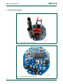
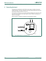
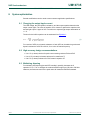
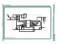
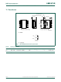
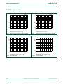
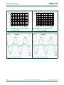
UM10735 SSL2101DB1169 230 V 5 W buck boost dimmable candle LED driver Rev. 1 — 11 November 2013 User manual Document information Info Content Keywords SSL2101DB1169, SSL2101T, mains dimmable, AC to DC conversion, buck boost, candle LE driver Abstract This user manual describes the SSL2101 mains 230 V 5 W candle buck boost dimmable demo board. UM10735 NXP Semiconductors SSL2101DB1169 230 V 5 W buck boost dimmable candle LED driver Revision history Rev Date Description v.1 20131111 first issue Contact information For more information, please visit: http://www.nxp.com For sales office addresses, please send an email to: [email protected] UM10735 User manual All information provided in this document is subject to legal disclaimers. Rev. 1 — 11 November 2013 © NXP B.V. 2013. All rights reserved. 2 of 17 UM10735 NXP Semiconductors SSL2101DB1169 230 V 5 W buck boost dimmable candle LED driver 1. Introduction WARNING Lethal voltage and fire ignition hazard The non-insulated high voltages that are present when operating this product, constitute a risk of electric shock, personal injury, death and/or ignition of fire. This product is intended for evaluation purposes only. It shall be operated in a designated test area by personnel qualified according to local requirements and labor laws to work with non-insulated mains voltages and high-voltage circuits. This product shall never be operated unattended. The SSL2101T is a highly integrated switching mode LED driver. It enables constant current driving from the mains input. The SSL2101T supports buck converter topology. It is suitable for non-isolated LED retrofit lamps. The application in this document is a compact 230 V mains dimmable LED driver for candle size 5 W input power. It improves dimmer compatibility by drawing strong bleeding current and weak bleeding current from the input. To reach the strict form factor, all the bleeding circuits are integrated. The application is energy saving because it uses the SSL2101 quasi-resonant switching technology. All values listed in this user manual are typical values unless otherwise specified. 2. Safety warning The board must be connected to the mains voltage. Touching the board during operation must be avoided at all times. An isolated housing is obligatory when used in uncontrolled, non-laboratory environments. Even though the secondary circuit with LED connection includes galvanic isolation, this isolation is not according to any norm. Thus, galvanic isolation of the mains phase using a variable transformer is always recommended. Figure 1 shows the symbols by which these devices can be recognized. 019aab174 019aab173 a. Isolated Fig 1. UM10735 User manual b. Not isolated Variable transformer (Variac) isolation symbols All information provided in this document is subject to legal disclaimers. Rev. 1 — 11 November 2013 © NXP B.V. 2013. All rights reserved. 3 of 17 UM10735 NXP Semiconductors SSL2101DB1169 230 V 5 W buck boost dimmable candle LED driver 3. Specification Table 1. UM10735 User manual SSL2101DB1169 specifications Symbol Parameter Condition Vi(mains) mains input voltage 207 V to 253 V; 50 Hz VO(LED) LED output voltage 30 V (DC) VO(ovp) overvoltage protection output voltage 60 V (DC) Io(LED) LED output current 128 mA Io(LED)ripple / Io(LED) LED output current ripple to LED output current ratio 13 %; nominal ILED = 128 mA IO(LED) / Vmains line regulation load current dependent 7.5 %; Vmains = 230 V 10 % IO(LED) / VO(LED) load regulation load current dependent 7 % at VLED 10 % efficiency 77 %; Vmains = 230 V (AC); VO(LED) = 30 V (DC) PF power factor 0.56; Vmains = 230 V (AC) THD total harmonic distortion < 66 % PCB size diameter = 28 mm EMC compliance meets EN55015 All information provided in this document is subject to legal disclaimers. Rev. 1 — 11 November 2013 Value © NXP B.V. 2013. All rights reserved. 4 of 17 UM10735 NXP Semiconductors SSL2101DB1169 230 V 5 W buck boost dimmable candle LED driver 4. Board photographs UM10735 User manual Fig 2. SSL2101DB1169 demo board (top) Fig 3. SSL2101DB1169 demo board (back) All information provided in this document is subject to legal disclaimers. Rev. 1 — 11 November 2013 © NXP B.V. 2013. All rights reserved. 5 of 17 UM10735 NXP Semiconductors SSL2101DB1169 230 V 5 W buck boost dimmable candle LED driver 5. Connecting the board The board can be optimized for a 230 V/50 Hz mains supply. In addition to the mains voltage optimization, the board is designed to work with multiple high-power LEDs with a total working voltage of between 28 V and 33 V. When attaching an LED load to an operational board (hot plugging) an inrush peak current occurs due to the discharge of the output capacitor. After a number of discharges, the LEDs can be damaged. Mount the board in a shielded or isolated box for demonstration purposes. /(' /(' 796 32:(5 ,1'8&725 GDPSHUUHVLVWRU / GDPSHUUHVLVWRU 1 ;FDS ),/0&$3 DDD Fig 4. UM10735 User manual SSL2101DB1169 board connections(top view) All information provided in this document is subject to legal disclaimers. Rev. 1 — 11 November 2013 © NXP B.V. 2013. All rights reserved. 6 of 17 UM10735 NXP Semiconductors SSL2101DB1169 230 V 5 W buck boost dimmable candle LED driver 6. Dimmers NXP Semiconductors have tested several TRIAC and transistor-based dimmers. Table 2 shows a list of dimmers that have been tested with the board. Table 2. List of tested dimmers Manufacturer IO(LED) no dimming (mA) IO(LED) minimum dimming (mA) IO(LED) maximum dimming (mA) Stability Clipsal 32E450LM 129 10 111 smooth HPM legrand 129 25 100 smooth Berker2819 129 45 115 smooth; increase damper resistor (R1) to 150 Berker2873 129 16 108 smooth GIRA030000/I01 129 46 114 smooth; increase damper resistor (R1) to 150 GIRA118400/I00 129 22 110 smooth; increase damper resistor (R1) to 150 LICHTERGLER 129 3 115 smooth BUSH2200 129 29 109 smooth BUSH2250U 129 5 112 smooth Chinese dimmer 01 129 40 126 smooth NVC 129 49 126 smooth Chinese dimmer 02 129 54 128 smooth Clipsal 32V500 series 129 5 116 smooth UM10735 User manual All information provided in this document is subject to legal disclaimers. Rev. 1 — 11 November 2013 © NXP B.V. 2013. All rights reserved. 7 of 17 UM10735 NXP Semiconductors SSL2101DB1169 230 V 5 W buck boost dimmable candle LED driver 7. Functional description The SSL2101T is an LED driver IC that operates directly from the rectified mains. It uses on-time mode control and frequency control to control the LED brightness. The BRIGHTNESS and PWMLIMIT pins can be used to control the LED output current when an external dimmer is connected. 7.1 Start-up and VCC supply The charging current flows from high-voltage DRAIN pin via an internal start-up current source to the VCC pin. The IC starts switching when the voltage on the VCC pin passes the VCC(startup) level. The auxiliary winding of the transformer can take over the supply when VCC is high enough and the supply from the line is stopped for high-efficiency operation. 7.2 Frequency setting External RC components on pins RC and RC2 control the timing of an internal oscillator. The internal oscillator sets the converter frequency. The frequency can be modulated to an upper and lower value using the BRIGHTNESS pin. 7.3 Bleeding The IC has two bleeding circuits that ensure proper dimmer operation The two circuits are called weak bleeder (pin WBLEED) and strong bleeder (pin SBLEED). When the voltage on both pins is lower than 52 V, the SBLEED switches on providing a current path that loads the dimmer. 7.4 Output Short Protection (OSP) When the LEDs are short-circuited, the demagnetization time is much longer than during normal operation because the voltage (Vf) of diode D3 determines the demagnetized slope. The valley switch circuit keeps the MOSFET switched off until the demagnetization time has passed. The work frequency is very low during a short circuit event, which limits the input power. 7.5 Output OverVoltage Protection (OVP) Zener diode D5 and the VCC pin are positioned in parallel to detect output overvoltage. Because of the ratio between the auxiliary wind and the primary winding, the VCC voltage increases with the output voltage until it reaches the threshold of diode D5. Diode D5 acts as a voltage fuse when an overvoltage event occurs. It breaks down and shorts VCC to GND. UM10735 User manual All information provided in this document is subject to legal disclaimers. Rev. 1 — 11 November 2013 © NXP B.V. 2013. All rights reserved. 8 of 17 UM10735 NXP Semiconductors SSL2101DB1169 230 V 5 W buck boost dimmable candle LED driver 8. System optimization Several modifications can be made to meet customer application specifications. 8.1 Changing the output ripple current The LED voltage, the LED dynamic resistance, and the output capacitor determine the output current ripple. The value of capacitor C3 is chosen to optimize the capacitor size and the light output. A ripple of 25 % results in an expected light output deterioration of < 1 %. The size for the buffer capacitor can be estimated from Equation 1: I LED 1 C out = ----------- ----------------------------------------------I 6 f mains R dynamic (1) For a series of LEDs, the dynamic resistance of each LED can be added to get the total dynamic resistance. At 50 Hz or 60 Hz, fmains is the AC mains frequency. 8.2 High-accuracy design recommendations • Use 1 % (or better) devices for peak current sensing resistors R14 and R15 • Use 10 % (or better) inductance tolerance for transformer T1 • Use 5 % (or better) tolerance for COG ceramic capacitor C7 8.3 Multistring dimming For multistring LED dimming (several LED candles in parallel), decrease the X capacitor C1 to 4.7 nF. It changes the conductive EMI margin from 150 kHz to 500 kHz. However, the final scan result of the peak value still meets the EN55015 standard. UM10735 User manual All information provided in this document is subject to legal disclaimers. Rev. 1 — 11 November 2013 © NXP B.V. 2013. All rights reserved. 9 of 17 xxxxxxxxxxxxxxxxxxxxx xxxxxxxxxxxxxxxxxxxxxxxxxx xxxxxxx x x x xxxxxxxxxxxxxxxxxxxxxxxxxxxxxx xxxxxxxxxxxxxxxxxxx xx xx xxxxx xxxxxxxxxxxxxxxxxxxxxxxxxxx xxxxxxxxxxxxxxxxxxx xxxxxx xxxxxxxxxxxxxxxxxxxxxxxxxxxxxxxxxxx xxxxxxxxxxxx x x xxxxxxxxxxxxxxxxxxxxx xxxxxxxxxxxxxxxxxxxxxxxxxxxxxx xxxxx xxxxxxxxxxxxxxxxxxxxxxxxxxxxxxxxxxxxxxxxxxxxxxxxxx xxxxxxxx xxxxxxxxxxxxxxxxxxxxxxxxx xxxxxxxxxxxxxxxxxxxx xxx NXP Semiconductors UM10735 User manual 9. Schematic 5 ' 1 8 5 & 5 5 5 5 ' & ' & /(' 5 5 / EHDG 5 8 6%/((' :%/((' 9&& 9&& *1' *1' 5 %5,*+71(66 5 5& 5& 5 & 5 66/ 5 /(' *1' & *1' 5 *1' $8; &( 7 '5$,1 6285&( & 5 5 5 ,6(16( ' 3:0/,0,7 9&& & ' & & 5 SSL2101DB1169 schematic UM10735 10 of 17 © NXP B.V. 2013. All rights reserved. Fig 5. DDD SSL2101DB1169 230 V 5 W buck boost dimmable candle LED driver Rev. 1 — 11 November 2013 All information provided in this document is subject to legal disclaimers. / / / UM10735 NXP Semiconductors SSL2101DB1169 230 V 5 W buck boost dimmable candle LED driver 10. Bill Of Material (BOM) Table 3. SSL2101DB1169 bill of material Reference Description and value Part number Manufacturer C1 X capacitor; ceramic; 10 nF; 250 V (AC) GRM55D7U3A103JW31L Murata C2 capacitor; ceramic; 22 nF; 630 V; 1210 GHM1335X7T223K630D500 Murata C3 capacitor; film; 330 nF; 400 V; P = 10 mm - Fara C5 capacitor; ceramic; 4.7 F; 25 V; X7R; 0805 - Murata C6 capacitor; ceramic; 10 F; 50 V; X5R; 1206 GRM31CR61H106KA Murata C7 capacitor; ceramic; 330 pF; 50 V; 0603; X7R; 5 % - Murata C12 capacitor; ceramic; 1 nF; 25 V; 0603; X7R - Murata C13 capacitor; ceramic; 2.2 nF; 630 V; X7T; 1206 GHM1530X7R222K630D500 Murata C14 capacitor; ceramic; 47 nF; 250 V; X7R; 1206 GR331BD72E473KW01L Murata CE1 capacitor; electrical; 100 F; 63 V; 105; 8 15 mm - - D1; D3 fast recovery diode; 600 V; 1 A; SMA ES1J Diotec D2 TVS diode; 500 W; SMA SMAJ440A Micro Commercial Components D4 switching diode; 200 V; 0.2 A; SOD123F BAS21H NXP Semiconductors D5 Zener diode; 27 V; SOD323F BZX84J-B27 NXP Semiconductors L1 drum inductor; power; 3.3 mH; 6 8 mm - - L4 EMI suppression ferrite bead; 0805 WE-CBF 742792097 WE Electronic L5 Inductor; axial; 1.3 mH; 0408 - - R1 resistor; axial; 120 ; 2 W - Yageo R2 resistor; axial; 100 ; 1 W - Yageo R3; R4 resistor; chip; 750 k; 5 %; 1206 - Yageo R5; R10; R18 resistor; chip; 15 k; 1 %; 0603 - Yageo R6; R7 resistor; chip; 180 k; 5 %; 1206 - Yageo R8; R9 resistor; chip; 1.1 k; 5 %; 1206 - Yageo R11 resistor; chip; 6.2 k; 1 %; 0603 - Yageo R12 resistor; chip; 56 k; 1 %; 0603 - Yageo R13 resistor; chip; 4.3 k; 5 %; 0805 - Yageo R14 resistor; chip; 2 ; 1 %; 0805 - Yageo R15 resistor; chip; 8.2 ; 1 %; 0805 - Yageo R16 resistor; chip; 100 k; 5 %; 0805 - Yageo R17 resistor; chip; 1 ; 5 %; 0805 - Yageo R19 resistor; chip; 100 k; 5 %; 0603 - Yageo T1 transformer; 1.1 mH; ER11.5 750341915 Wurth Electronics Midcom U1 IC; SSL2101; SO-16 - NXP Semiconductors U2 bridge rectifier; 0.5 A; 600 V; MB6S - Vishay UM10735 User manual All information provided in this document is subject to legal disclaimers. Rev. 1 — 11 November 2013 © NXP B.V. 2013. All rights reserved. 11 of 17 UM10735 NXP Semiconductors SSL2101DB1169 230 V 5 W buck boost dimmable candle LED driver 11. Transformer GRWORFDWHVWHUP QRWFKORFDWHVWHUPVLGH PD[ PD[ PD[ ORWFRGHDQGGDWHFRGH WHUPQR VIRUUHIRQO\ DDD a. Bobbin 35, $8; DDD b. Schematic Fig 6. Table 4. SSL2101DB1169 transformer specification Winding information Number Section Wire N1 pins 1 to 2 0.12 mm * 1UEW 108 1 2 N2 pins 7 to 4 0.12 mm * 1UEW 56 7 4 UM10735 User manual Turns Begin pin All information provided in this document is subject to legal disclaimers. Rev. 1 — 11 November 2013 End pin Description 1.1 mH ± 10 % © NXP B.V. 2013. All rights reserved. 12 of 17 UM10735 NXP Semiconductors SSL2101DB1169 230 V 5 W buck boost dimmable candle LED driver 12. Performance data Ș DDD DDD 3) 9PDLQV9 Efficiency at Vmains = 230 V 10 % Fig 7. DDD Fig 8. Line regulation UM10735 User manual 9PDLQ9 Power factor as a function of mains voltage DDD 9PDLQ9 Line regulation at Vmains = 230 V 10 % Fig 9. OR P$ Power factor at Vmains = 230 V Efficiency as a function of mains voltage OR P$ 9R9 Load regulation at Vmains = 230 V 10 % Fig 10. Load regulation All information provided in this document is subject to legal disclaimers. Rev. 1 — 11 November 2013 © NXP B.V. 2013. All rights reserved. 13 of 17 UM10735 NXP Semiconductors SSL2101DB1169 230 V 5 W buck boost dimmable candle LED driver DDD OR P$ DDD SRZHUORVV : ĭPV ĭPV Fig 11. LED current loss as a function of dimmer conduction angle () Fig 12. Power loss as a function of dimmer conduction angle () Fig 13. Input voltage waveform Fig 14. Output voltage waveform UM10735 User manual All information provided in this document is subject to legal disclaimers. Rev. 1 — 11 November 2013 © NXP B.V. 2013. All rights reserved. 14 of 17 UM10735 NXP Semiconductors SSL2101DB1169 230 V 5 W buck boost dimmable candle LED driver 13. EMC performance a. L-line b. N-line Fig 15. EMC conducted emission line a. Horizontal b. Vertical Fig 16. EMC radiated emission UM10735 User manual All information provided in this document is subject to legal disclaimers. Rev. 1 — 11 November 2013 © NXP B.V. 2013. All rights reserved. 15 of 17 UM10735 NXP Semiconductors SSL2101DB1169 230 V 5 W buck boost dimmable candle LED driver 14. Legal information 14.1 Definitions Draft — The document is a draft version only. The content is still under internal review and subject to formal approval, which may result in modifications or additions. NXP Semiconductors does not give any representations or warranties as to the accuracy or completeness of information included herein and shall have no liability for the consequences of use of such information. Export control — This document as well as the item(s) described herein may be subject to export control regulations. Export might require a prior authorization from competent authorities. 14.2 Disclaimers Limited warranty and liability — Information in this document is believed to be accurate and reliable. However, NXP Semiconductors does not give any representations or warranties, expressed or implied, as to the accuracy or completeness of such information and shall have no liability for the consequences of use of such information. NXP Semiconductors takes no responsibility for the content in this document if provided by an information source outside of NXP Semiconductors. In no event shall NXP Semiconductors be liable for any indirect, incidental, punitive, special or consequential damages (including - without limitation - lost profits, lost savings, business interruption, costs related to the removal or replacement of any products or rework charges) whether or not such damages are based on tort (including negligence), warranty, breach of contract or any other legal theory. Notwithstanding any damages that customer might incur for any reason whatsoever, NXP Semiconductors’ aggregate and cumulative liability towards customer for the products described herein shall be limited in accordance with the Terms and conditions of commercial sale of NXP Semiconductors. Right to make changes — NXP Semiconductors reserves the right to make changes to information published in this document, including without limitation specifications and product descriptions, at any time and without notice. This document supersedes and replaces all information supplied prior to the publication hereof. Suitability for use — NXP Semiconductors products are not designed, authorized or warranted to be suitable for use in life support, life-critical or safety-critical systems or equipment, nor in applications where failure or malfunction of an NXP Semiconductors product can reasonably be expected to result in personal injury, death or severe property or environmental damage. NXP Semiconductors and its suppliers accept no liability for inclusion and/or use of NXP Semiconductors products in such equipment or applications and therefore such inclusion and/or use is at the customer’s own risk. Applications — Applications that are described herein for any of these products are for illustrative purposes only. NXP Semiconductors makes no representation or warranty that such applications will be suitable for the specified use without further testing or modification. Customers are responsible for the design and operation of their applications and products using NXP Semiconductors products, and NXP Semiconductors accepts no liability for any assistance with applications or customer product design. It is customer’s sole responsibility to determine whether the NXP Semiconductors product is suitable and fit for the customer’s applications and products planned, as well as for the planned application and use of customer’s third party customer(s). Customers should provide appropriate design and operating safeguards to minimize the risks associated with their applications and products. UM10735 User manual NXP Semiconductors does not accept any liability related to any default, damage, costs or problem which is based on any weakness or default in the customer’s applications or products, or the application or use by customer’s third party customer(s). Customer is responsible for doing all necessary testing for the customer’s applications and products using NXP Semiconductors products in order to avoid a default of the applications and the products or of the application or use by customer’s third party customer(s). NXP does not accept any liability in this respect. Evaluation products — This product is provided on an “as is” and “with all faults” basis for evaluation purposes only. NXP Semiconductors, its affiliates and their suppliers expressly disclaim all warranties, whether express, implied or statutory, including but not limited to the implied warranties of non-infringement, merchantability and fitness for a particular purpose. The entire risk as to the quality, or arising out of the use or performance, of this product remains with customer. In no event shall NXP Semiconductors, its affiliates or their suppliers be liable to customer for any special, indirect, consequential, punitive or incidental damages (including without limitation damages for loss of business, business interruption, loss of use, loss of data or information, and the like) arising out the use of or inability to use the product, whether or not based on tort (including negligence), strict liability, breach of contract, breach of warranty or any other theory, even if advised of the possibility of such damages. Notwithstanding any damages that customer might incur for any reason whatsoever (including without limitation, all damages referenced above and all direct or general damages), the entire liability of NXP Semiconductors, its affiliates and their suppliers and customer’s exclusive remedy for all of the foregoing shall be limited to actual damages incurred by customer based on reasonable reliance up to the greater of the amount actually paid by customer for the product or five dollars (US$5.00). The foregoing limitations, exclusions and disclaimers shall apply to the maximum extent permitted by applicable law, even if any remedy fails of its essential purpose. Safety of high-voltage evaluation products — The non-insulated high voltages that are present when operating this product, constitute a risk of electric shock, personal injury, death and/or ignition of fire. This product is intended for evaluation purposes only. It shall be operated in a designated test area by personnel that is qualified according to local requirements and labor laws to work with non-insulated mains voltages and high-voltage circuits. The product does not comply with IEC 60950 based national or regional safety standards. NXP Semiconductors does not accept any liability for damages incurred due to inappropriate use of this product or related to non-insulated high voltages. Any use of this product is at customer’s own risk and liability. The customer shall fully indemnify and hold harmless NXP Semiconductors from any liability, damages and claims resulting from the use of the product. Translations — A non-English (translated) version of a document is for reference only. The English version shall prevail in case of any discrepancy between the translated and English versions. 14.3 Trademarks Notice: All referenced brands, product names, service names and trademarks are the property of their respective owners. All information provided in this document is subject to legal disclaimers. Rev. 1 — 11 November 2013 © NXP B.V. 2013. All rights reserved. 16 of 17 UM10735 NXP Semiconductors SSL2101DB1169 230 V 5 W buck boost dimmable candle LED driver 15. Contents 1 2 3 4 5 6 7 7.1 7.2 7.3 7.4 7.5 8 8.1 8.2 8.3 9 10 11 12 13 14 14.1 14.2 14.3 15 Introduction . . . . . . . . . . . . . . . . . . . . . . . . . . . . 3 Safety warning . . . . . . . . . . . . . . . . . . . . . . . . . . 3 Specification. . . . . . . . . . . . . . . . . . . . . . . . . . . . 4 Board photographs . . . . . . . . . . . . . . . . . . . . . . 5 Connecting the board . . . . . . . . . . . . . . . . . . . . 6 Dimmers . . . . . . . . . . . . . . . . . . . . . . . . . . . . . . . 7 Functional description . . . . . . . . . . . . . . . . . . . 8 Start-up and VCC supply . . . . . . . . . . . . . . . . . . 8 Frequency setting . . . . . . . . . . . . . . . . . . . . . . . 8 Bleeding . . . . . . . . . . . . . . . . . . . . . . . . . . . . . . 8 Output Short Protection (OSP) . . . . . . . . . . . . . 8 Output OverVoltage Protection (OVP) . . . . . . . 8 System optimization . . . . . . . . . . . . . . . . . . . . . 9 Changing the output ripple current . . . . . . . . . . 9 High-accuracy design recommendations . . . . . 9 Multistring dimming. . . . . . . . . . . . . . . . . . . . . . 9 Schematic . . . . . . . . . . . . . . . . . . . . . . . . . . . . . 10 Bill Of Material (BOM) . . . . . . . . . . . . . . . . . . . 11 Transformer . . . . . . . . . . . . . . . . . . . . . . . . . . . 12 Performance data. . . . . . . . . . . . . . . . . . . . . . . 13 EMC performance . . . . . . . . . . . . . . . . . . . . . . 15 Legal information. . . . . . . . . . . . . . . . . . . . . . . 16 Definitions . . . . . . . . . . . . . . . . . . . . . . . . . . . . 16 Disclaimers . . . . . . . . . . . . . . . . . . . . . . . . . . . 16 Trademarks. . . . . . . . . . . . . . . . . . . . . . . . . . . 16 Contents . . . . . . . . . . . . . . . . . . . . . . . . . . . . . . 17 Please be aware that important notices concerning this document and the product(s) described herein, have been included in section ‘Legal information’. © NXP B.V. 2013. All rights reserved. For more information, please visit: http://www.nxp.com For sales office addresses, please send an email to: [email protected] Date of release: 11 November 2013 Document identifier: UM10735