1
MICRO LAMBDA WIRELESS, INC.
YIG based Products
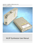
MLSP Synthesizer User Manual
MICRO LAMBDA WIRELESS, INC.
MLSP Synthesizer
User Manual
Micro Lambda Wireless, Inc.
46515 Landing Pkwy. Fremont, CA 94538
Phone 510.770.9221 • Fax 510.770.9213
Rev B 3/6/2013
Table of Contents
Section
1.0
2.0
3.0
4.0
4.1
4.2
5.0
5.1
5.2
5.3
6.0
6.1
7.0
8.0
9.0
10.0
Description
Introduction
Package contents
General overview of product capabilities
Setup and operation
Connections
MLSP operation
Controlling the MLSP using a personal computer
Installing the documentation and control software
USB interface
USB HID PC interface example, C# source code
Serial interface
Serial interface timing diagram
Communication syntax
Hardware installation information
Technical support
Warranty
1
Page
2
2
2
5
5
6
6
6
6
8
9
10
11
13
13
13
1.0 Introduction
This manual describes the setup, operation and remote communication for the MLSP
Synthesizer. The model and serial numbers are located on the label located on the top
cover of the unit. Each unit has a separate, custom specification sheet for the particular
model defining the synthesizer’s frequency range, RF characteristics and options.
General operating/programming instructions are located herein.
The CD Rom supplied with the package contains a SetupMLSP.msi file, when
executed, will create a folder named “MLSP Support Files” on the desktop containing
short cuts to the manual, documentation and programs for interfacing the product with a
personal computer. This SetupMLSP.msi file is compatible with Windows XP, Windows
Vista and Windows 7. The most current versions of these files, new offerings and
standard synthesizer specifications can be downloaded at our web site:
http://www.microlambdawireless.com
2.0 Package Contents
Item
MLSP Series Synthesizer
DC Power mating connector
USB A male to USB Mini-B cable
CD Rom (Contains manual, quick start guide and PC software)
MLSP Quick Start Guide (Printed)
Quantity
Purchased Qty.
Purchased Qty.
Purchased Qty.
1 each
1 each
3.0 General Overview of Product Capabilities
The MLSP series of YIG-Based synthesizers can be supplied in wideband or
narrowband models and are ideal as the main local oscillators in receiving systems,
frequency converters and test and measurement equipment. They provide 1 kHz
frequency resolution over the 600 MHz to 20.1 GHz frequency range. Power levels of
+8 to +13 dBm are provided throughout the series and full band tuning speed is 3 - 6
mSec. The units are 5” x 3” x 1” high and fit a 2 slot PXI chassis. Standard frequency
ranges are 0.6 to 2.5 GHz, 2 to 8 GHz, 6 to 18 GHz and 8 to 20 GHz. The MLSP can be
configured with an internal OCXO with a stability of < +/- 1.0 ppm or an external
reference signal in the 1 - 200 MHz range. Two types of interface come standard: USB
for trouble free connection to a personal computer and a 5 wire serial interface for use
in the customers system. Outline drawings 181-001 and 181-002 shown on the next
two pages define two of the possible mechanical configurations. These drawings are
displayed mainly for the mechanical and the connection information, many other
configurations and options are available. See your model specification sheet or contact
Micro Lambda Wireless, Inc. for details. Operating temperature ranges outside the 0 to
60 Deg. C range are also available.
2
.99
WARRANTY LABEL
.00
.00
MICRO LAMBDA WIRELESS, INC.
J3
.35
.60
2.08
2.30
2.63
2x .28
.00
.99
.54
2.85
3.00
14
J1
1
.88
J2
STATIC LABEL
2.29
.00
LABEL
J4
.15
.40
5.17
.15
.00
4.85
5.00
.17 MAX.
TOP - #4 THRU HOLE
C'SINK 82° x .220 Ø
BOTTOM - #8 HELICOIL
(4) PLACES
WARRANTY LABEL
.38 MAX.
-J1 MALE:
- MOLEX# 35363-1460
- J1 POWER SUPPLY INPUTS REQUIRED FOR USB OPERATION
-J1 MATES WITH:
- MOLEX# 35507-1400
- J1 RECOMMENDED WIRE SIZE = A.W.G. 22-24
-CRIMP PIN:
- MOLEX# 50212-8000
(*) ACTIVE LOW
J1
35363-1460
1
+15 VDC, +12V OPT.
J2
USB MINI-B
1
+V
J1
35363-1460
2
+15 VDC, +12V OPT.
J2
USB MINI-B
2
D-
J1
35363-1460
3
GROUND
J2
USB MINI-B
3
D+
J1
35363-1460
4
GROUND
J2
USB MINI-B
4
GND
J1
35363-1460
5
+ 5 VDC
J2
USB MINI-B
5
GND
J1
35363-1460
6
+ 5 VDC
J1
35363-1460
7
J1
35363-1460
8
N/C
J1
35363-1460
9
CLOCK
J3
SMA-FEMALE
1
REF. INPUT
J1
35363-1460
10
DATA IN
J4
SMA-FEMALE
1
RF OUTPUT
J1
35363-1460
11
SELECT (*)
J1
35363-1460
12
BUSY
J1
35363-1460
13
LOCK ALARM
J1
35363-1460
14
DATA OUT
UNLESS OTHERWISE SPECIFIED DIMENSIONS
ARE IN INCHES
TOLERANCE ARE :
FRACTIONS
DECIMALS
.02
.xx
.xxx .010
CONTRACT NO.
ANGLES
APPROVALS
DRAWN
WEIGHT
15 Oz. / 425gr
FINISH
N/C
N.NGUYEN
MICRO LAMBDA WIRELESS, INC.
DATE
10/03/11
ENGR.
MANUF.
SIZE
Q.A.
DO NOT SCALE DRAWING
CAGE No
0RN63
3
DWG. NO.
181 - 001
REV.
A
.99
WARRANTY LABEL
2x .28
.00
LABEL
MICRO LAMBDA WIRELESS, INC.
1
2.08
2.30
2.63
.00
.99
.54
2.85
3.00
14
J1
STATIC LABEL
.88
J2
.00
.35
.60
5.17
.38 MAX.
.15
.00
2.23
J3
4.85
5.00
.54
J4
.15
.00
.17 MAX.
TOP - #4 THRU HOLE
C'SINK 82° x .220 Ø
BOTTOM - #8 HELICOIL
(4) PLACES
WARRANTY LABEL
-J1 MALE:
- MOLEX# 35363-1460
- J1 POWER SUPPLY INPUTS REQUIRED FOR USB OPERATION
-J1 MATES WITH:
- MOLEX# 35507-1400
- J1 RECOMMENDED WIRE SIZE = A.W.G. 22-24
-CRIMP PIN:
- MOLEX# 50212-8000
(*) ACTIVE LOW
J1
35363-1460
1
+15 VDC, +12V OPT.
J2
USB MINI-B
1
+V
J1
35363-1460
2
+15 VDC, +12V OPT.
J2
USB MINI-B
2
D-
J1
35363-1460
3
GROUND
J2
USB MINI-B
3
D+
J1
35363-1460
4
GROUND
J2
USB MINI-B
4
GND
J1
35363-1460
5
+ 5 VDC
J2
USB MINI-B
5
GND
J1
35363-1460
6
+ 5 VDC
J1
35363-1460
7
J1
35363-1460
8
N/C
J1
35363-1460
9
CLOCK
J3
SMA-FEMALE
1
REF. INPUT
J1
35363-1460
10
DATA IN
J4
SMA-FEMALE
1
RF OUTPUT
J1
35363-1460
11
SELECT (*)
J1
35363-1460
12
BUSY
J1
35363-1460
13
LOCK ALARM
J1
35363-1460
14
DATA OUT
UNLESS OTHERWISE SPECIFIED DIMENSIONS
ARE IN INCHES
TOLERANCE ARE :
FRACTIONS
DECIMALS
.xx
.02
.xxx .010
CONTRACT NO.
ANGLES
APPROVALS
DRAWN
WEIGHT
15 Oz. / 425gr
FINISH
N/C
N.NGUYEN
MICRO LAMBDA WIRELESS, INC.
DATE
10/03/11
ENGR.
MANUF.
SIZE
Q.A.
DO NOT SCALE DRAWING
CAGE No
0RN63
4
DWG. NO.
181 - 002
REV.
A
A simple block diagram is shown in Figure 1. Depending on the port configuration as
shown in drawing 181-001 & 181-002, the synthesizer provides a external reference input
J3, a RF output J4, a DC power/serial interface port J1, and a USB Mini-B interface
connector J2. The synthesizer is tuned via the J1 serial connection or the USB port J2.
DC voltages of +5.0V and +15.0V, with adequate current to operate the product must be
applied to J1 in order to communicate with the product.
+5VDC (J1)
Figure 1.
Opt. Amp.
YIG
Osc.
+15VDC (J1)
USB I/O (J2)
CPU /
Memory
Serial I/O (J1)
Frequency
control
and
calibration
Opt. OCXO
RF Out (J4)
Fractional
PLL /
Prescalers
and Opt. Ref.
PLL.
REF In (J3)
4.0 Setup and Operation
This product is designed for a 0 to 60 Degree C environment and should not be
subjected to humidity >95%. Use proper ESD handling procedures. Allow for a proper
heat-sink able to dissipate the total wattage/heat generated at the highest frequency
setting of the unit. Verify that all external RF/microwave cables and components
connected to the unit are in good working condition.
4.1 Connections
Connect to the preferred interface port, Serial or USB. USB Mini-B to USB Male - A
cable for connection to a host PC USB port, the USB interface is USB 1.1 and 2.0
compatible. The serial port is a 0-5V, CMOS/TTL compatible port; it is very similar to an
SPI communication port. Clock, Data and Select/Enable operate in the typical serial
communication format, except that the maximum clock speed is 250 kHz. The Busy line
is for handshake to the controller, a High on this line tells the controller that the
synthesizer is busy and should not be selected for communication at this time. The Data
Out line is used to read data from the synthesizer if a command requested it. The data
is clocked into the controller by clocking out data of 0’s to the MLSP and the controller
reads during this time. The Data Out line will be taken high by the MLSP, when data is
ready. The Busy line must be monitored. See section 6.0/6.1 serial communication for
details. The Lock Alarm signal J1 pin 13 is a hardware logic signal that shows the state
of the internal phase locked loop circuits.
5
This line should be a TTL high for the majority of the time unless the unit is stepping
frequency, then it will pulse low when switching between frequencies, typically it will be
low for less than 2 milliseconds.
Connect an external reference frequency (if required) to J3. Connect a +5.0 VDC and a
+15 VDC power supply with adequate current to operate the product (see spec sheet) to
the J1 connector; +5.0 VDC on J1 pins 5 and 6, +15.0VDC on J1 pins 1 and 2 and a
common ground for both supplies on pins 3 and 4. Note the power supply inputs are
protected from damage up to +/-20 VDC.
4.2 MLSP operation
Turn on the power supply voltages and verify that the current for each supply is below
the maximum stated current in the specifications for your model. A 5 minute warm up is
recommended before use. The unit should be operating at the last frequency it was set
to before power down; this would typically be Fmin when shipped from the factory. The
Lock Alarm line (J1 pin 13) should be high.
5.0 Controlling the MLSP using a personal computer
The MLSP Synthesizer can be controlled by a personal computer for Demo purposes.
The requirements for this are as follows: A USB ver. 1.1 or 2.0 port on the PC, Windows
XP, Windows Vista or Windows 7 (32 or 64 bit), the programs included on the MLSP
Support CD and a power supply capable of supplying the DC Voltage and Current
required to operate the MLSP synthesizer.
5.1 Installing the documentation and control software
The CD ROM supplied with the MLSP contains the file named SetupMLSP.msi.
Execute this file to install the manual, documentation and control programs for PC
interface. The setup file, when run, will create a folder named “MLSP Support Files” on
the computer desktop with short cuts to the documentation and interface program.
(Note: This setup file must be executed for the USB PC interface program to operate
correctly, dll files will be installed to the system directory.)
5.2 USB Interface
The MLSP product, when connected using the USB interface, appears as a USB HID
device (Human Interface Device) to the Windows operating system. The USB HID
driver is supplied with the windows operating system, and is installed automatically
when the unit is connected to the PC’s USB port.
The MLSP may be controlled remotely via a USB connection using the supplied “MLSP
PC interface.exe” program. A screen capture of this program is shown in Figure 2.
Additional information is accessed via the program’s pull-down menus “File” and “Help”.
Included in these menus are View/Print the configuration NOVO locations and data, a
list of all commands that the unit will respond to, how to build a wire harness to connect
to power supplies and a PC printer port and a description of NOVO locations and what
is stored at each location. On the program screen you will see some limited information
6
about the unit. PLL Lock status is also shown; it is updated each time the “Update Info”
check box is selected. Commands may be sent to and received from the unit. The unit
can also be stepped up and down in frequency using the “Step Up” and “Step Down”
buttons, the frequency will increment and decrement based on the frequency shown in
the step size box. This number can be changed to any valid step size within the
frequency range limits of the unit. The current frequency setting is also shown. The
program can be used to connect to multiple units; all units that are connected to the
PC’s USB ports will show up in the pull down list in the “Choose Unit #” box. If units are
added after the program has been initiated or the MLSP(s) were powered down for a
time, press the “Refresh” button to update the list. A sweep mode feature is included to
allow the unit to sweep (Step and Dwell) at each frequency based on the step size and
dwell time text boxes. Start and Stop frequency can also be adjusted for a narrower
range, if needed. Four sweep modes are selectable; Auto = continuous sweep across
the start/stop range retraces from stop frequency and repeats. Single = one single
sweep from start to stop. Manual = unit will take one step up or down from the current
frequency when the step up/down keys are pressed. Frequency List mode = frequency
sweep based on a user generated list of frequencies. To configure this mode, click the
Edit List button and input one frequency per line (In MHz, i.e. 2450.125) in the text
editor and save/exit. The file is created and named for the serial number of the unit.
Make sure the List Mode is selected and choose your desired sweep mode, then press
Run. The unit will step the frequency based on your list of frequencies and the dwell
time selected. Frequencies can be increasing, decreasing or random. Multiple versions
of the program can be executed to sweep or communicate with more than one unit at a
time.
Figure 2
7
5.3 USB HID PC Interface example C# source code
Included in the installed support files folder is an example of a simple USB HID interface
program written in C#. The project file and source code were written using Microsoft
Visual Studio Express 2010, C Sharp. Visual Studio Express 2010, C Sharp can be
downloaded for free at http://www.microsoft.com/visualstudio/en-us/products/2010editions/visual-csharp-express. After you register this free version of the programming
environment, you can create and edit C# programs.
This source code will allow you to get started integrating the MLSP USB communication
into your own C programs. The example program is a simple interface in which you can
send and receive ASCII characters. The interface tests for a connection to the MLSP
synthesizer by looking for a return string indentifying the MLSP unit after searching
through all attached USB devices.
An executable version of the program is located on the CD in the directory - \MLSP USB
HID PC Interface C# Example\bin\x86\Release\. The file name is – MLSP USB HID PC
Interface C Example.exe. A screen shot of the interface is shown in figure 3.
Figure 3
8
6.0 Serial interface
The MLSP can be programmed using a 5 wire serial bus. The timing diagram is shown in
Figure 4. The Five control lines are as follows:
SELECT
(J1 – Pin 11)
Input
CLOCK
(J1 – Pin 9)
Input
DATA IN
(J1 – Pin 10)
Input
BUSY
(J1 – Pin 12)
Output
DATA OUT
(J1 – Pin 14)
Output
Active Low. Enables the shifting of data into the internal command buffer. Also
serves as a command terminator when it goes HIGH. The status of the BUSY line
should be checked before activating this line. Note: All command + data, command
strings must be sent using a single Select Line Cycle. When low, Busy is high.
Data is clocked into the unit on the rising edge (Positive Edge Clocked) and DATA
OUT is valid at this time. The maximum clock rate of this line is 2 usec. For best
performance the status of the DATA OUT line should be checked before sending the
first Clock. This line should be maintained in a LOW state at the application of Select
to prevent confusion.
Input data pin. Data is sent MSB first. Data must be stable 1 usec. Before the
CLOCK line goes high and 1 usec. After the clock goes low. (Setup / Hold time)
This line is used to indicate that the unit is busy processing other commands or
doing its internal housekeeping. Before sending a Select = TRUE the status of this
line should be checked to ensure that it is LOW (NOT Busy). Any command initiated
by setting Select Low while BUSY is High may result in lost data and uncertain
results.
NOTE: The unit can be programmed without using this line if sufficient time is
allowed between Clocks and between commands. The time required varies between
commands. This mode is not recommended as there are some events that occupy
the microcontroller other than the serial communications.
This line is used to pass internal information from the synthesizer to the user. Data
is guaranteed to be valid on the falling edge of the clock signal. Data is sent out
MSB first. In addition, this line is used as a communication ‘handshake’ line. Once
SELECT has gone LOW the DATA OUT line will be taken HIGH to indicate that the
unit is listening. It will remain HIGH until the first data is sent out which is initiated by
the first rising edge of CLOCK. DATA OUT will be returned to LOW after Select has
been released.
For the following information, please reference the above documentation regarding Busy
and Data out.
Recommended send data sequence: The format is one select per command string. The
string length is variable up to 16 ASCII characters. A decimal point is required for resolution
less than 1.0 MHz. The unit will accept a frequency command with a resolution of 1.0 Hz, and
it will try to get as close to the frequency requested as it can, typically <= 10.0 Hz accuracy. So
the command to set the frequency F8000.1 would be sent as follows: Set select low, clock out
01000110 00111000 00110000 00110000 00110000 00101110 00110001 (Ignore spaces,
only used to single out each ASCII char), then set select high. The unit should go to 8000.1
MHz. When select goes high, this tells the unit that the user is done and to start interpreting
the command. If the command is not understood, the unit will do nothing.
Recommended read data sequence: The returned data is variable in length; however it is
recommended that the full 16 bytes of data be read to clear the buffer. Set select low, send the
desired read command and set select high. The unit interprets the command and places the
requested data in its buffer. Then set select low and clock out 16 ASCII nulls while clocking in
the data, then set select high. Example: To read the units internal temperature, set select low
and send ASCII T (01010100), set select high. Set select low and send 16 00000000 while
reading the data line and clocking in bits. Set select high. The information should be similar to
+25.0C, in ASCII. All of the memory locations in the unit can be read in this manner, using the
R command.
9
In addition to the lines above there is a unit status line, LOCK ALARM status (J1- Pin 13),
which is a static line. This TTL output (High = Locked) indicates the overall health of the unit –
specifically, that all of the internal phase locked loops are locked.
The MLSP serial interface lines operate on internal 3.3V logic of a PIC microcontroller; this
should allow the unit to communicate in systems operating with 2.5V, 3.3V and 5.0V serial
control lines.
6.1 Serial interface timing diagram:
Select
TCH
Clock
TCL
Dat a
TSU
Dat aOut
T CS
TSC
TSB
Busy
Figure 4
Tsc > 2 usec select low before first clock
Tcs > 2 usec clock low before chip select high
Tsu > 2 usec data stable before rising edge of clock
Tch > 2 usec minimum clock high time
Tcl > 2 usec minimum clock low time
Tsb > 10 usec (time to wait before sampling ‘BUSY’)
Data/Clock Setup time = >1 usec.
Data/Clock Hold time = Tch + 1 usec.
10
7.0 Communication syntax
The following table describes the commands that the MLSP supports. This is a custom
syntax created by Micro Lambda Wireless, Inc. All commands are sent and received in
ASCII format. The commands are NOT case sensitive. These commands can be used
with all forms of communication (USB and Serial).
Command
?
Function
Comment
Report Status – Bits, D0 = 100 MHz lock, D1 = YIG PLL, D6 = self test,
Typical return = 11000011
D7 = NOVO lock
F
Frequency (ASCII) (Dec. #)
L
Set Level of RF Power option (Option G)
ASCII freq in MHz: xxxxx.xxxxxx; (example: F12345.678900)
Sets the Leveling DAC to a specific Level (L-0.5) (L9.5)
MR
Recall a user saved frequency setting from memory location (MR25)
0-99, stored @ NOVO location 200-299
MS
Save current frequency setting of unit to memory location (MS75)
0-99, stored @ NOVO location 200-299
POWERON Turns ON internal supplies related to +15V input
Turns ON YIG / PLL / Analog supplies. (default = on power up)
POWEROFF Turns OFF internal supplies related to +15V input (Low power state)
Digital logic and Xtal Osc. Supplies are always on
R
SP
Read a NOVO location
R0 returns model number
Synthesizer preset to factory settings.
Copy NOVO Loc. 900-960 to 0-60
SR
Soft PIC Reset
Reset PIC, clear var. run PIC code from start; (example: SR)
ST
Self Test
Execute internal test; 1 = Pass; (example: SR, then read data)
Read internal temp.
Returns ASCII chars, reading in Deg. C; (example: T, then read
data)
V1
Read YIG PLLV (typical Range = 1V to 12V)
6.75V = normal; (example: V1, then read data)
V2
Read 100 MHz PLL V (typical Range = 1V to 12V)
5.00V = normal; (example: V2, then read data)
V3
Read internal +2.5V voltage
2.50V = normal; (example: V3, then read data)
V4
Read internal +3.3V voltage
3.30V = normal; (example: V4, then read data)
V5
Read internal +5.0V voltage
5.00V = normal; (example: V5, then read data)
V6
Read internal +6.75V voltage
6.75V = normal; (example: V6, then read data)
V7
Read internal +12.0V voltage
12.00V = normal; (example: V7, then read data)
V8
Read internal +13.5V voltage
13.50V = normal; (example: V8, then read data)
V9
Read internal -5.0V voltage
-5.00V = normal; (example: V9, then read data)
R0000
Model Number (Example = R0) Read Location 0.
MLSP-0208CD
16 Bytes)
R0001
Serial Number
0002
R0002
Internal Xtal Serial Number (Optional)
0940-002
R0003
Fmin, in MHz
2000 (unit is tunable 100.0 MHz below Fmin.)
R0004
Fmax, in MHz
8000 (unit is tunable 100.0 MHz above Fmax.)
R0005
Current Internal Reference Frequency Setting - MHz
R# = 1 – 200 MHz, typ. = 100
R0006
RF min, in dBm
10.0
R0007
RF max, in dBm
15.0
R0008
Temp min, in Deg. C
0
R0009
Temp max, in Deg. C
60
R0010
Highest Temp reached, in Deg. C
59.8
R0011
NOVO State - Locked/Unlocked
Locked
R0012
Firmware Version & date
1.5 Nov 16 2011
R0013
Unit Health Status – “Good” or Self test failure information
Good or Fail V5 as example
R0014
Unit Calibration Status - Yes/No
Yes
R0015
Self Test Results - Pass/Fail
Pass
R0016
Current Output Frequency setting - MHz
2500
R0017
Internal Xtal Setting – Int or Ext or ExtXtal
ExtXtal
Xtal.)
R0018
Xtal DAC cal # (Hex)
0000-FFFF
R0019
Coarse DAC Fmin cal # (Hex)
0000-FFFF
T
11
("W" blocked with NOVO locked.) (R/W =
(3 modes; Internal Xtal, External and External with
Command
Function
Comment
R0020
Coarse DAC Fmax cal # (Hex)
0000-FFFF
R0021
Current Coarse DAC setting (Hex)
0000-FFFF
R0022
Current Fine DAC interpolated setting (Hex)
0000-FFFF, 8000 nominal
R0023
Current Loop Gain (CP) setting, 0-31 (Dec)
31 charge pump current
R0024
Current Microwave Divider (DV) setting, 1, 2 ,4 ,8 (Dec)
2
(Sets external Prescaler to 1, 2, 4, or 8)
R0025
Current Reference divider setting
2
Ref Div
R0026
Coarse Cal status; Yes / No
Yes
R0027
Fine Cal status; Yes / No
Yes
R0028
Xtal Cal status; Yes / No / N/A
Yes N/A if Internal Xtal setting = Ext or ExtXtal
R0029
External reference freq. In MHz for 100 MHz PLL (ExtXtal mode)
i.e.: 10 = 10 MHz external reference. 1.0 MHz increments only
R0030
Current loop gain (LG) setting; 0-127 (Dec), U29 gain setting.
written by PIC after LG command, read at boot and sent to U29
R0031
Customer part number, if shown on P.O.
123-45-6789 (Shown on unit label as PN:)
R0032
Frequency resolution in MHz (or Step Size)
0.001 = 1.0 kHz
R0033
Spurious Spec., in dBc
-60
R0034
Harmonics Spec., in dBc
-12
R0035
Phase Noise Spec. @ 100 Hz Offset, in dBc/Hz
-85
R0036
Phase Noise Spec. @ 1 kHz Offset, in dBc/Hz
-90
R0037
Phase Noise Spec. @ 10 kHz Offset, in dBc/Hz
-100
R0038
Phase Noise Spec. @ 100 kHz Offset, in dBc/Hz
-120
R0039
Phase Noise Spec. @ 1 MHz Offset, in dBc/Hz
-140
R0040
Switching Speed, any step, in mS
5.0
R0041
+15V Supply current Max, in mA
750
R0042
+5V Supply current Max, in mA
300
R0043
Level Control Option installed?
Yes / No
R0044
Level Control Maximum Power Limit, in dB
10.0
R0045
Level Control Minimum Power Limit, in dB
-10.0
R0046
Level Control Cal Point Frequency Step (Cal data taken every - ___ MHz)
100.0 MHz
R0047
Level Control Cal Point Level step (Cal data taken every - ___ dB)
1.0
R0048
Current RF Level Setting, in dBm
9.5
R0049
Current Level DAC setting (Hex, ASCII)
AF61
R0050
Level Control CAL Status (Is Level option calibrated)
Yes / No
R0051
Level flatness Spec. in +/- dB (+/- 2.0 = 4.0 total)
2.0
R0058
MLWI Sales (Job) number
18-0024
R0059
MLWI Product Outline Drawing # and Revision
181-003 G
Power State (Power supplies on or off) On power-up will default to ON!
"ON" or "OFF"(Low power) - Show status of "poweron" and
"poweroff" commands.
User Saved / Recalled frequency setting locations, (0-99)
Frequency stored in MHz
Config data backup safe area, SF - save factory stores data here.
Backup copy of NOVO location 0000 to 0060 (Config Data)
DAC cal data, stored in 25 MHz increments, Fmin-100 to Fmax+100
MHz, 8000 Nom.
Stored in 16 bit HEX numbers (ASCII format)
R0052
R0053
R0054
R0055
R0056
R0057
R0060
….
200-299
….
R 900-960
….
R10002047
12
8.0 Hardware installation information
The unit may be installed into a system using four #4-40 X 1.25” long flat head screws,
inserted from the top, in the 4 corner mounting holes. Alternately, four #8-32 X 0.5”
screws can be attached from the bottom side through the mounting surface, in the 4
corner mounting holes. The Molex connector (J1) and the mating connector information
are shown in the drawing numbers 181-001 and 181-002 in this document. The USB
connector is the standard Mini-B style.
9.0 Technical Support
For Technical support please contact:
Micro Lambda Wireless, Inc.
46515 Landing Pkwy.
Fremont, CA 94538
Ph: (510) 770-9221
Fax: (510) 770-9213
Email: [email protected]
You can visit our website at http://www.microlambdawireless.com for updated
information, specifications and downloads.
10.0 Warranty
Seller warrants for a period of twelve (12) months from the date of original shipment that
the products will be free from defects in material and workmanship and design (if of
Micro Lambda Wireless, Inc. design) and will be in conformity with applicable
specifications and drawings and all other contractual requirements. However, this
warranty shall not apply to any product which that has been subjected to misuse,
misapplication, accident, improper installation, neglect, unauthorized repair, alteration,
adjustment, inundation or fire. See the complete warranty and return policy document
number 201-005 Rev- at our website at http://www.microlambdawireless.com.
13