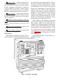
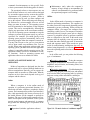
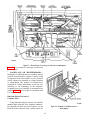
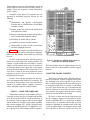
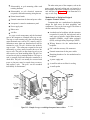
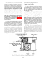
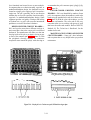
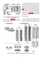
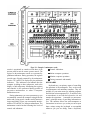
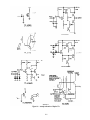
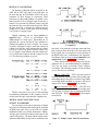
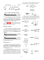
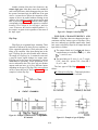
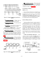
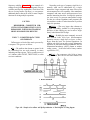
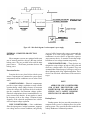
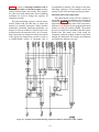
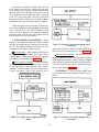
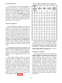
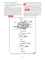
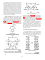
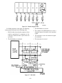
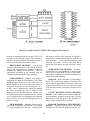
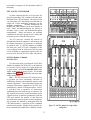
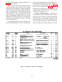
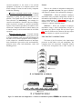
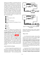
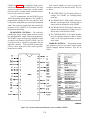
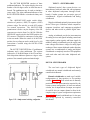
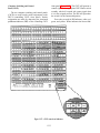
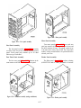
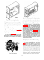
1
NONRESIDENT
TRAINING
COURSE
March 1997
Electronics Technician
Volume 6—Digital Data Systems
NAVEDTRA 14091
DISTRIBUTION STATEMENT A: Approved for public release; distribution is unlimited.
Although the words “he,” “him,” and
“his” are used sparingly in this course to
enhance communication, they are not
intended to be gender driven or to affront or
discriminate against anyone.
DISTRIBUTION STATEMENT A: Approved for public release; distribution is unlimited.
PREFACE
By enrolling in this self-study course, you have demonstrated a desire to improve yourself and the Navy.
Remember, however, this self-study course is only one part of the total Navy training program. Practical
experience, schools, selected reading, and your desire to succeed are also necessary to successfully round
out a fully meaningful training program.
COURSE OVERVIEW: After completing this nonresident training course, you will demonstrate a
knowledge of the subject matter by correctly answering questions on the following broad topics:
fundamentals and operations of computers, computer configurations and hardware, computer operator
controls and controlling units, computer components and circuits, central processing units and buses,
computer memories, input/output (I/O) and interfacing, computer instructions and man/machine interfaces,
magnetic tape storage, magnetic disk storage, CD-ROM storage, printers, data conversion devices, and
switchboards.
THE COURSE: This self-study course is organized into subject matter areas, each containing learning
objectives to help you determine what you should learn along with text and illustrations to help you
understand the information. The subject matter reflects day-to-day requirements and experiences of
personnel in the rating or skill area. It also reflects guidance provided by Enlisted Community Managers
(ECMs) and other senior personnel, technical references, instructions, etc., and either the occupational or
naval standards, which are listed in the Manual of Navy Enlisted Manpower Personnel Classifications
and Occupational Standards, NAVPERS 18068.
THE QUESTIONS: The questions that appear in this course are designed to help you understand the
material in the text.
VALUE: In completing this course, you will improve your military and professional knowledge.
Importantly, it can also help you study for the Navy-wide advancement in rate examination. If you are
studying and discover a reference in the text to another publication for further information, look it up.
1997 Edition Prepared by
DSCS(SW/AW) Robert M. Maynard
Published by
NAVAL EDUCATION AND TRAINING
PROFESSIONAL DEVELOPMENT
AND TECHNOLOGY CENTER
NAVSUP Logistics Tracking Number
0504-LP-026-7570
i
Sailor’s Creed
“I am a United States Sailor.
I will support and defend the
Constitution of the United States of
America and I will obey the orders
of those appointed over me.
I represent the fighting spirit of the
Navy and those who have gone
before me to defend freedom and
democracy around the world.
I proudly serve my country’s Navy
combat team with honor, courage
and commitment.
I am committed to excellence and
the fair treatment of all.”
ii
CONTENTS
CHAPTER
PAGE
1. Fundamentals and Operations of Computers . . . . . . . . . . . . 1-1
2. Computer Configurations and Hardware . . . . . . . . . . . . . . . 2-1
3. Computer Operator Controls and Controlling Units . . . . . . . 3-1
4. Computer Components and Circuits . . . . . . . . . . . . . . . . . . 4-1
5. Central Processing Units and Buses.. . . . . . . . . . . . . . . . . 5-1
6. Computer Memories . . . . . . . . . . . . . . . . . . . . . . . . . . . . 6-1
7. Input/Output (I/O) and Interfacing . . . . . . . . . . . . . . . . . . . 7-1
8. Computer Instructions and Man/Machine Interfaces . . . . . . . 8-1
9. Magnetic Tape Storage . . . . . . . . . . . . . . . . . . . . . . . . . . . 9-1
10. Magnetic Disk Storage . . . . . . . . . . . . . . . . . . . . . . . . . . 10-1
11. CD-ROM Storage . . . . . . . . . . . . . . . . . . . . . . . . . . . . . 11-1
12. Printers . . . . . . . . . . . . . . . . . . . . . . . . . . . . . . . . . . . 12-1
13. Data Conversion Devices and Switchboards . . . . . . . . . . . 13-1
APPENDIX
I. Glossary of Terms and Acronyms.. . . . . . . . . . . . . . . . . AI-1
II. References Used to Develop the TRAMAN . . . . . . . . . . . AII-1
INDEX . . . . . . . . . . . . . . . . . . . . . . . . . . . . . . . . . . . . . . . INDEX-1
iii
CREDITS
Trademark Credits
Adobe and PostScript are registered trademarks of Adobe Systems, Inc.
in the U.S. and other countries.
AMP and TERMI-POINT are registered trademarks of AMP Incorporated.
Canon is a registered trademark of Canon U. S.A., Inc.
Centronics is a registered trademark of Centronics Corp.
IBM and OS/2 are registered trademarks of International Business
Machines Corporation.
Intel 80286 is a registered trademark of Intel Corporation.
LaserJet is a registered trademark of Hewlett-Packard Company.
Lin CMOS is a registered trademark of Texas Instruments Incorporated.
Microsoft and MS-DOS are registered trademarks of Microsoft Corporation.
UNIX and ST (straight Tip) are registered trademarks of AT&T.
iv
SUMMARY OF THE ELECTRONICS
TECHNICIAN TRAINING SERIES
This series of training manuals was developed to replace the Electronics Technician 3 & 2 TRAMAN. The content is directed to personnel
working toward advancement to Electronics Technician Second Class.
The nine volumes in the series are based on major topic areas with
which the ET2 should be familiar. Volume 1, Safety, provides an
introduction to general safety as it relates to the ET rating. It also provides both general and specific information on electronic tag-out procedures, man-aloft procedures, hazardous materials (i.e., solvents, batteries,
and vacuum tubes), and radiation hazards. Volume 2, Administration, discusses COSAL updates, 3-M documentation, supply paperwork, and other
associated administrative topics. Volume 3, Communications Systems,
provides a basic introduction to shipboard and shore-based communication
systems. Systems covered include man-pac radios (i.e., PRC-104, PSC-3)
in the hf, vhf, uhf, SATCOM, and shf ranges. Also provided is an introduction to tactical data links (Link-4, Link-11) and the Communications
Link Interoperability System (CLIPS). Volume 4, Radar Systems, is a
basic introduction to air search, surface search, ground controlled approach,
and carrier controlled approach radar systems. Volume 5, Navigation Systems, is a basic introduction to navigation systems, such as OMEGA,
SATNAV, TACAN, and man-pac systems. Volume 6, Digital Data Systems, is a basic introduction to digital data systems and includes discussions about SNAP II, laptop computers, and desktop computers.
Volume 7, Antennas and Wave Propagation, is an introduction to wave
propagation, as it pertains to Electronics Technicians, and shipboard and
shore-based antennas. Volume 8, Support Systems, discusses system interfaces, troubleshooting, sub-systems, dry air, cooling, and power systems.
Volume 9, Electro-Optics, is an introduction to night vision equipment,
lasers, thermal imaging, and fiber optics.
v
INSTRUCTIONS FOR TAKING THE COURSE
assignments. To submit your
answers via the Internet, go to:
ASSIGNMENTS
The text pages that you are to study are listed at
the beginning of each assignment. Study these
pages carefully before attempting to answer the
questions. Pay close attention to tables and
illustrations and read the learning objectives.
The learning objectives state what you should be
able to do after studying the material. Answering
the questions correctly helps you accomplish the
objectives.
http://courses.cnet.navy.mil
Grading by Mail: When you submit answer
sheets by mail, send all of your assignments at
one time. Do NOT submit individual answer
sheets for grading. Mail all of your assignments
in an envelope, which you either provide
yourself or obtain from your nearest Educational
Services Officer (ESO). Submit answer sheets
to:
SELECTING YOUR ANSWERS
Read each question carefully, then select the
BEST answer. You may refer freely to the text.
The answers must be the result of your own
work and decisions. You are prohibited from
referring to or copying the answers of others and
from giving answers to anyone else taking the
course.
COMMANDING OFFICER
NETPDTC N331
6490 SAUFLEY FIELD ROAD
PENSACOLA FL 32559-5000
Answer Sheets: All courses include one
“scannable” answer sheet for each assignment.
These answer sheets are preprinted with your
SSN, name, assignment number, and course
number. Explanations for completing the answer
sheets are on the answer sheet.
SUBMITTING YOUR ASSIGNMENTS
To have your assignments graded, you must be
enrolled in the course with the Nonresident
Training Course Administration Branch at the
Naval Education and Training Professional
Development
and
Technology
Center
(NETPDTC). Following enrollment, there are
two ways of having your assignments graded:
(1) use the Internet to submit your assignments
as you complete them, or (2) send all the
assignments at one time by mail to NETPDTC.
Grading on the Internet:
Internet grading are:
•
•
assignment
Do not use answer sheet reproductions: Use
only the original answer sheets that we
provide—reproductions will not work with our
scanning equipment and cannot be processed.
Follow the instructions for marking your
answers on the answer sheet. Be sure that blocks
1, 2, and 3 are filled in correctly. This
information is necessary for your course to be
properly processed and for you to receive credit
for your work.
Advantages to
COMPLETION TIME
you may submit your answers as soon as
you complete an assignment, and
you get your results faster; usually by the
next working day (approximately 24 hours).
Courses must be completed within 12 months
from the date of enrollment. This includes time
required to resubmit failed assignments.
In addition to receiving grade results for each
assignment, you will receive course completion
confirmation once you have completed all the
vi
PASS/FAIL ASSIGNMENT PROCEDURES
For subject matter questions:
If your overall course score is 3.2 or higher, you
will pass the course and will not be required to
resubmit assignments. Once your assignments
have been graded you will receive course
completion confirmation.
E-mail:
Phone:
[email protected]
Comm: (850) 452-1001, Ext. 1713
DSN: 922-1001, Ext. 1713
FAX: (850) 452-1370
(Do not fax answer sheets.)
Address: COMMANDING OFFICER
NETPDTC N315
6490 SAUFLEY FIELD ROAD
PENSACOLA FL 32509-5237
If you receive less than a 3.2 on any assignment
and your overall course score is below 3.2, you
will be given the opportunity to resubmit failed
assignments. You may resubmit failed
assignments only once. Internet students will
receive notification when they have failed an
assignment--they may then resubmit failed
assignments on the web site. Internet students
may view and print results for failed
assignments from the web site. Students who
submit by mail will receive a failing result letter
and a new answer sheet for resubmission of each
failed assignment.
For enrollment, shipping,
completion letter questions
grading,
or
E-mail:
Phone:
[email protected]
Toll Free: 877-264-8583
Comm: (850) 452-1511/1181/1859
DSN: 922-1511/1181/1859
FAX: (850) 452-1370
(Do not fax answer sheets.)
Address: COMMANDING OFFICER
NETPDTC N331
6490 SAUFLEY FIELD ROAD
PENSACOLA FL 32559-5000
COMPLETION CONFIRMATION
After successfully completing this course, you
will receive a letter of completion.
NAVAL RESERVE RETIREMENT CREDIT
ERRATA
If you are a member of the Naval Reserve, you
may earn retirement points for successfully
completing this course, if authorized under
current directives governing retirement of Naval
Reserve personnel. For Naval Reserve retirement, this course is divided into two units
evaluated at 21 points.
Errata are used to correct minor errors or delete
obsolete information in a course. Errata may
also be used to provide instructions to the
student. If a course has an errata, it will be
included as the first page(s) after the front cover.
Errata for all courses can be accessed and
viewed/downloaded at:
Unit 1: 12 points upon satisfactory completion
of Assignments 1 through 8.
http://www.advancement.cnet.navy.mil
STUDENT FEEDBACK QUESTIONS
Unit 2: 9 points upon satisfactory completion
of Assignments 9 through 14.
We value your suggestions, questions, and
criticisms on our courses. If you would like to
communicate with us regarding this course, we
encourage you, if possible, to use e-mail. If you
write or fax, please use a copy of the Student
Comment form that follows this page.
(Refer to Administrative Procedures for Naval
Reservists on Inactive Duty, BUPERSINST
1001.39, for more information about retirement
points.)
vii
Student Comments
Course Title:
Electronics Technician, Volume 6—Digital Data Systems
NAVEDTRA:
14091
Date:
We need some information about you:
Rate/Rank and Name:
SSN:
Command/Unit
Street Address:
City:
State/FPO:
Zip
Your comments, suggestions, etc.:
Privacy Act Statement: Under authority of Title 5, USC 301, information regarding your military status is
requested in processing your comments and in preparing a reply. This information will not be divulged without
written authorization to anyone other than those within DOD for official use in determining performance.
NETPDTC 1550/41 (Rev 4-00
ix
CHAPTER 1
FUNDAMENTALS AND OPERATIONS
OF COMPUTERS
INTRODUCTION
The computer is the heart and soul of any data system. It can be packaged in
many sizes and configurations. It may be a general- or special-purpose type. It
may handle analog or digital data, or both. It may be referred to as a mainframe,
minicomputer, or microcomputer. Regardless of what it is called or how it is
configured, it will share certain common fundamental concepts and principles with
all other computers. All computers gather, process, store, disseminate, and display
data and information. Each computer is housed in a frame or cabinet. Each has a
central processing unit (CPU), memory, input/output (I/O) section, and a power
supply. How these are assembled in each computer will vary from unit to unit.
How much computing power a computer has is defined by the technology it
uses and NOT by its physical size. A more powerful computer means greater speed,
greater capacity and capability to store information, and a greater facility to
accommodate additional peripheral (external) equipment. Our objective is to teach
you the basic fundamentals and concepts of a computer, no matter what type you
maintain.
After completing this chapter, you should be able to:
Describe the functions and purposes of a computer
Differentiate between computer types based on their hardware
characteristics
Recognize the uses of computers and their functional operation
Describe the types of computers used with tactical, tactical support, and
nontactical programs
Differentiate between full capability, reduced capability, and battle
short mode in terms of computer operation and performance
Compare the operational modes of computers including modes used in
operation and maintenance
Describe the security requirements associated with computers
Before you begin study of how a computer operates, let’s take a look at the
fundamentals and operations of computers in general. These include their
functions, the different types of computers, and their functional operation. Also
included are their operational uses, configuration/setups, and modes of operation.
1-1
TOPIC 1—COMPUTER FUNCTIONS
AND TYPES
Systems such as the fire control system
Subsystems such as the combat direction system
The computers the Navy uses vary from
mainframes to microcomputers. Regardless of the
types of computers and their operational uses, their
functions are basically the same. Depending on the type
of computer and the operational use, the methods will
vary. First, we discuss the functions of computers, the
different ways computers handle data, and the methods
they use to accomplish this. Then we discuss the
functional operation of computers.
Data processing systems (another computer and
conversion devices)
Display systems via sensors (radar)
Communication systems such as data links and
local-area networks (LANs)
Many computer systems are designed to gather data
using a combination of both the manual and automatic
methods.
COMPUTER FUNCTIONS
All computers must be able to gather, process, store,
disseminate, and display data.
Process Data
Processing data is the main function and the
purpose of the computer. There are other systems,
subsystems, and equipment that will work with the
computer to help gather, store, disseminate, and display
data; but processing the data is exclusively the
computer’s function. The heart of the computer—the
place where the data is processed in a computer—is
called the central processing unit (CPU). Figure 1-1
shows the basic configuration of a digital computer.
Gather Data
All computers, no matter what their size, must gather
data before they can process the data. The operational
program will dictate how the data is gathered—
manually, automatically, or a combination of both.
Manually, an operator or technician will input the
data to the computer. This can be done either directly
or by a device external to the computer. The following
are commonly used input devices:
After the data is processed, it can be stored,
disseminated, or displayed.
l Keyboards
Store Data
. Display consoles
The computer can store data either internally or
externally. Internally, the computer uses memory
. Data terminals
l Computer maintenance panels
l Storage devices (magnetic tape units, disk drive
units, and paper tape units)
As an example, an operator at a console will input data
via the console to the computer and the computer will
process the data for storage, dissemination, or display
depending on the functions of the operational program.
Data may be input from a console using pushbuttons,
switches, toggles, or a combination of these.
Automatically gathering data means the computer
receives data from another system, subsystem, or
equipment. The computer monitors for external
requests through a series of programmed requests and
acknowledges. The computer first sees the gathered
data when it comes through the input section of the
input/output section of the computer. Then depending
on the operational program, the computer will either
react immediately or store the data for future use. The
following are examples of the sources from which
computers gather the data automatically:
Figure 1-1.—A basic functional composition of a digital
computer.
1-2
banks. These memory banks can hold instructions and
both processed and unprocessed data. Memory access
time and memory capacity are the other main factors
that determine how powerful a computer is.
subsystem such as a display or communication
subsystem. This is a very useful tool when you are
performing maintenance, both preventive and
corrective. Figure 1-2 is an example of a maintenance
console panel. Notice the indicator lights for the I/O
controller, I/O timing, Mode, Central Processor
Register, and soon. These will provide you with status
information. For example, you can monitor the I/O
controller register to see if the computer is interfacing
with a particular subsystem such as display or
communications. Look to see if the indicator of that
channel is illuminated (either flashing or constantly lit).
Or, you could look at the contents of a particular register
in the CPU by selecting that register while installing a
patch to a program using an inspect and change
procedure or utility.
Externally, computers can store data on magnetic
disks (hard and floppy), magnetic tape, or paper tape.
Disk drive units offer quicker access to the data than
magnetic or paper tape units. On some systems, the
disks can store more data than the internal memory of
a computer. The amounts of each will depend on the
design and requirements of the data system. Some
systems internally store and process the data. Others
depend heavily on the disks to hold and store the data,
bringing the data into memory for processing, and then
storing the results back onto disk.
Disseminate Data
TYPES OF COMPUTERS
After the computer has processed the data, it can
send it to the I/O section or an I/O unit for immediate
or future dissemination to various equipments. The
data will exit the output section of the computer’s
input/output section. It can be sent to an output device
such as a printer, or to one of many storage devices such
as a magnetic tape or disk unit. It can also be sent to a
subsystem, such as a display system, via its associated
equipment.
In general terms, computers can be classified into
mainframe computers,
three categories:
minicomputers, and microcomputers. A computer’s
power is determined by the technology it uses, NOT its
physical size. Greater speed, greater capability and
capacity to store information, and greater facility to
accommodate additional peripheral (external)
equipment will make one computer more powerful than
another regardless of their overall physical sizes. We
do not go into detail on each of the different types of
computers. Rather, we identify examples of each and
point out their physical and internal differences. This
will prove valuable when you are maintaining them.
Let’s take a look at the types of computers you will
maintain in the Navy. Later in this manual, you will
study the internal workings of computers—their basic
functional operation.
Display Data
Computer systems display two general types of
data—data related to the mission of the system and
status information related to operation of the system and
hardware performance. The computer relies on
peripheral equipment, such as printers and display
units, to display the processed data—the mission related
output of the operational program. Your interest in
output generally relates to whether the data is sent
properly by the computer and is displaying properly. In
other words, you want to know the computer system is
functioning properly. The content of the data is usually
a secondary interest to you and a primary interest to the
user/operator.
Mainframe Computers
Mainframe computers are physically the largest
computers you will maintain. Their ruggedness makes
them better suited than microcomputers and
minicomputers to handle the mechanical shock and
vibration, salt spray, temperature and humidity found
aboard Navy vessels. The mainframes you will
maintain are general-purpose, digital data computers
with multiprocessing capability.
The other type of data/information that can be
displayed relates to the operation of the system. This
includes operator information, system error messages,
and indications of system problems. You will be
particularly interested in this information. The
maintenance panels and data terminals can display
real-time data and provide you with current status of the
operational program. For example, the maintenance
panels of some computers have registers where the
presence or absence of indicator lamps can indicate to
the technician if the computer is communicating with a
Mainframe computers are considered the heart of
the afloat and ashore tactical and tactical support data
systems. These mainframe computers are big, fret,
multiprocessor computers with correspondingly large
memories and multiple I/O channel capabilities. They
process large volumes of data and require a lot of
program flexibility. Their operational programs are
1-3
Figure 1-2.—Example of a maintenance console panel of a digital computer.
and/or adapter unit with I/O connectors, heat
complex, and as systems are updated, the programs
exchangers for each module or unit, power supply
must be revised to meet the new demands of the fleet.
unit(s), and blower motors for cooling.
Operational programs for mainframe computers are
supported by technical teams external to the command.
Two examples of mainframes are the AN/UYK-7(V)
and the AN/UYK-43(V) computers. They are
general-purpose, militarized, digital data computers
with large-scale memories, I/O capabilities, and
multiprocessing capabilities that allow a number of
CPUs to operate simultaneously in the same system.
They interface with other mainframes and peripherals
in the data processing subsystem, the display
subsystem, and the communication subsystem.
Training is obtained through formal C schools and is
NEC producing. Figure 1-3 is an example of one of the
Navy’s mainframe computers.
Some physical features of mainframe computers
are highlighted as follows:
l Large rugged frame or cabinet —Contains
individual modules or units; central processor unit
(CPU), memory modules, input/output controller
Figure 1-3.—Example of a mainframe computer.
1-4
for tactical and tactical support operations. They are
also built for ruggedness. Minicomputers are capable
of stand-alone or self-contained operation, or of being
an embedded processor in a system or other type of
digital device. Minicomputers are generally used in
applications that don’t require the faster computational
speeds or larger memory capacities available on
mainframes. These computers also have program
flexibility. Minicomputers receive external technical
support for the operational programs they use. The
programs for minicomputers are updated as specific
jobs or applications are updated and revised.
l Operator console —Controls operation of the
computer at the computer. This console/panel is
usually located above the logic chassis but separate
from the maintenance console/panel. It contains the
controls and indicators necessary to initiate computer
operations. You can turn on power to the system and
load the operational program and start its execution.
. Remote console —Controls operation of the
computer from a remote location. Performs the same
functions as an operator console except it does not apply
power to computer set.
l Maintenance console panel/display control unit
(DCU) —Controls operation of the computer and is
used to perform maintenance (preventive and
corrective).
Minicomputers
Some examples of minicomputers are the minis
used as interface computers with communications or
radar systems. Minis are also used as the host
computers for the Shipboard Nontactical ADP Program
(SNAP I, SNAP II, and SNAP III) Systems. Training
for minicomputers is provided through formal A, C, and
FTC schools and may be NEC producing. SNAP
system training is an example of an NEC-producing
school. Figure 1-4 is an illustration of a typical
minicomputer.
Minicomputers are mid-range computers. They are
smaller in physical size than the large mainframes used
Some physical features of minicomputers are
highlighted as follows:
l Specific power requirements (frequency and
voltage).
l Specific cooling requirements (air and/or liquid
cooling).
Figure 1-4.—Example of a minicomputer.
1-5
civilian contractor schools, and OJT. Training for
micros is not NEC producing. Figure 1-5 is an
illustration of a typical microcomputer.
l Large to medium rugged frame or cabinet —
Some frames or cabinets use a stationary or sliding
chassis or assemblies or stationary racks or card cages
that contain individual modules or printed circuit
boards. The functional and support areas include a
central processor unit (CPU), memory units,
input/output controller boards for various peripherals,
I/O connectors, power supply unit(s), and blower
motors for cooling. (NOTE: Some minicomputer
frames or cabinets also contain the peripherals-disk
drive units, magnetic tape units, and paper tape units.)
The physical features of microcomputers are very
different from mainframes and minis. The following is
a brief description of a typical PC/desktop system.
l Small compact frame or cabinet —PCs are unique in that the frame or cabinet contains the majority of
the components for a complete system. A typical PC
frame or cabinet contains the following components:
Backplane or motherboard for printed circuit
boards
. Control and Maintenance Panel (CMP) or
computer control panel —Controls operation of the
computer and is used to perform maintenance
(preventive and corrective).
A central processor unit (CPU) and memory
printed circuit board(s) (pcb) (NOTE: In
some cases the CPU and memory are located
on the same pcb.)
l Specific power requirements (frequency and
voltage).
Input/output pcb
l Specific cooling requirements (air and/or liquid
cooling).
Disk controller pcb
Microcomputers
Video controller pcb
Microcomputers, personal computers (PCs), are
small, lightweight, and portable. Some of them are
more powerful than some of the older, larger
mainframes and minicomputers. Microcomputers are
unique in that the heart of the computer (the CPU) is
contained on a single integrated chip (IC) and the entire
computer system is contained on a handful of printed
circuit boards located inside a small compact frame or
cabinet. In some cases a complete microcomputer is
located on a single chip; the CPU, co-processor, and
memory. Some micros/PCs are high-speed, multi-user,
multi-tasking units. Traditionally micros are used for
word processing, database management, spreadsheets,
graphics, desktop publishing, and other general office
applications. Currently, micros and PCs are being
used for tactical support systems, such as Naval
Intelligence Processing Systems (NIPS) and Joint
Operational Tactical System (JOTS). Micros and PCs
can also be used as a SNAP system for shorebased
operational commands, such as ASWOC. The
operational programs for PCs used for a tactical
support system are supported externally by technical
teams. These operational programs are also updated as
systems are added or replaced. Programs that are used
for word processing, graphics, and so on are abundant
and can be obtained through civilian vendors and
software support teams such as Commander Naval
Computer and Telecommunications Command
(COMNAVCOMTELCOM). Training for microcomputers is obtained through formal A schools,
Data storage devices: Hard disk drive units,
floppy disk drive units, and/or tape cassette
units
I/O connector: Parallel or serial communications
A small fan: No special cooling requirements; the unit relies on ambient temperature
of the room or space
Power supply: No special requirements
l Display monitor — Display monitors are output
devices for visual displays of data, and may have
monochrome or color displays.
Figure 1-5.—Example of a microcomputer.
1-6
Keyboard —Keyboards are input devices used to
control operation of a computer.
Tactical Systems
. Printer —Printers are output devices for
producing printed material.
A computer is the heart of the Combat Direction
System (CDS)/Naval Tactical Data System (NTDS),
which is a subsystem of the ship’s combat system.
CDS/NTDS receives data from ship’s sensors and other
ships using tactical data links. The CDS/NTDS consists
of high-speed digital computers, peripherals, displays,
communication links, and computer programs. The
CDS/NTDS hardware is divided into three major
equipment groups (subsystems) as follows:
●
. Modem —Modems are optional components
used to communicate with mainframes, minicomputers,
and microcomputers through existing phone lines.
Mouse —Another optional component is a
mouse. A mouse is an input device used to highlight
text, move the cursor, and select commands and
functions without using the keyboard. A mouse can be
used in combination with a keyboard to control
computer operations.
●
●
Data Processing Group
●
Data Display Group
●
Data Communications Group
The data these subsystems generate and feed back
to the data processing subsystem is stored, processed,
and distributed by the operational program. The
computer is part of the data processing group and
coordinates the operations within CDS/NTDS and
makes the information available to other major
subsystems within combat systems: radar/IFF, weapons
(guns, missiles, and underwater), electronic warfare,
and navigation. The CDS/NTDS is a real-time system.
The type of computer used in a tactical data system is a
mainframe such as the AN/UYK-7(V) or
AN/UYK-43(V) computer. The number of computers
used in a tactical data system depends on the class of
ship and its configuration/setup. Figure 1-6 is a portion
TOPIC 2—FUNCTIONAL OPERATION
OF COMPUTERS
At the heart of every data system is a computer. All
digital data made available on any system has been
processed by the computer. The computer oversees the
operation of any data system. Through a coordinated
series of interrupts, requests, and acknowledges, the
computer exchanges data with other computers,
peripherals, and the subsystems required for that
system.
The signal flow between systems, subsystems, and
equipment is all coordinated by the operational
program of the computer(s). Exchange of signals
between the systems, subsystems, and equipment is
accomplished through a coordinated series of priorities
where interrupts, requests, and acknowledges
determine when the data will be exchanged. The type
of data exchanged includes status signals, control
signals, and data words. Interfacing between the
computer(s) and other systems, subsystems, and
equipment requires some type of cabling-standard
shielded and unshielded cables, fiber-optic cables, and
ribbon cables, and their associated connectors.
Methods of interfacing include parallel and serial data
transfers.
OPERATIONAL USES OF COMPUTERS
You may have the opportunity of maintaining three
basic types of data systems: tactical, tactical support,
and nontactical. All three rely on one or more
computers to make rapid calculations and make
information available.
Figure 1-6.—Simplified block diagram of a tactical data
system (CDS/NTDS).
1-7
is used to effectively conduct battle-management of the
tactical situation. The JMCIS consists of a data
processing subsystem and a video processing subsystem. The data processing subsystem includes desktop
1
computers (DTC/TAC-n ) with single and dual
monitors, printer plotters, and printers. The video
processing subsystem includes high and low resolution
monitors, large screen displays, and video switch.
Communication between DTC/TAC-n in the data
processing subsystem and video processing subsystem
is accomplished via a Genser fiber-optic LAN. JMCIS
gathers data from a variety of external links including
OTCIXS, Flag communication, Fleet Broadcast, and
Link 11 or Link 14.
of a simplified block diagram of a typical CDS/NTDS
in a tactical data system.
Another example of a tactical data system is the
Integrated Tactical Amphibious Warfare Data System
(ITAWDS).
Tactical Support Systems
Tactical support platforms include a variety of
systems. Unlike tactical data systems, tactical support
systems generally use either mainframes or micros as
their operational computers. Depending on the system,
tactical support systems can use a single computer or a
multiple computer configuration. The computers in
tactical support systems also interface with other
computers, peripherals, displays, communication links,
and operational programs. Let’s look at three
examples: ASW systems, JMCIS, and NIPS.
NAVAL INTELLIGENCE PROCESSING
SYSTEM.— Naval Intelligence Processing System
(NIPS) integrates up-to-the-minute tactical intelligence
with national and fleet-produced database intelligence
information. Data is gathered from the Naval Modular
Automated Communication System (NAVMACS),
Ocean Surveillance Product (OSP), Generic Front End
Co-Processor (GFCP), Automatic Tracking Point
(ATP), Fleet Imagery Support Terminal (FIST), video
diskplayers, and optical disk recorders, and, in turn, is
disseminated to GFCP, ATP, and Tactical Aviation
Mission Planning System (TAMPS). The NIPS uses
the DTC/TAC-n in a LAN configuration as its
operational computers. The other hardware interfaces
include hard drives, color printers, plotters, tape backup
units, a camcorder, and light table. The NIPS uses both
MS-DOS and the UNIX operating system to process
and manage its mapping/imagery workstation and
message handler workstation. Depending on the vessel,
the NIPS can be a basic system, as on a multipurpose
amphibious assault ship (LHD), or it can be a much
larger system with multiple workstations and remotes,
as on a carrier (CV).
ASW SYSTEMS.— ASW systems deal primarily
with antisubmarine warfare. They provide active and
passive search, detection, tracking, and classification
operations necessary to engage and destroy subsurface
or surface targets. They support ASW airborne
systems. ASW systems include the Antisubmarine
Warfare Operations Center (ASWOC) and CarrierAntisubmarine Warfare Module (CV-ASWM) systems.
These systems use a single computer as their central
point of operation.
The computers in these systems interface with the
following subsystems or equipment within their
subsystem:
● Command and Control Subsystem —Controls
the data to and from this subsystem and other
subsystems through the ADP Subsystem and Display
Subsystem.
Communication Subsystem —Allows communication between Maritime Patrol Aircraft (MPA) or
Surface Units and/or ASWOCs, CV-ASWMs, and
FHLTs. Communication is via secure voice or secure
data networks.
●
Naval Tactical Command Support Systems
Naval Tactical Command Support Systems include
those systems that handle data used for administrative
purposes and office functions. They support
organizational and intermediate-level maintenance,
supply and financial management, and administrative
applications. The types of computers generally used are
minicomputers and microcomputers. Nontactical
systems include the Shipboard Nontactical ADP
Program (SNAP I, SNAP II, and SNAP III) Systems
and PC.
. Fast Time Analysis System (FTAS) Subsystem
(ASWOCs and CV-ASWMs only) —Analyzes acoustic
and nonacoustic data provided by mission aircraft.
JOINT MARITIME COMMAND INFORMATION SYSTEMS.— The Joint Maritime Command
Information Systems (JMCIS) is an informational data
system used to provide data to designated flagships. It
1-8
for programming the PC; they include BASIC,
FORTRAN, COBOL, PASCAL, C, and many others.
These languages allow you to design your own
programs to perform functions exactly the way you
want them. Figure 1-7 is a simplified block diagram of
a PC system.
SNAP SYSTEMS.— The SNAP systems are used
primarily to reduce the administrative workload
associated with equipment maintenance, supply and
financial management, and personnel administration.
Because the SNAP systems differ in their
subsystem configurations, we are only listing the
equipment with which they are both capable of
interfacing. Some SNAP systems communicate via
modems and specialized interfacing techniques and
hardware. SNAP computers interface with the
following equipment:
A PC can interface with other hardware. The
following are examples:
Secondary storage units—hard disk drive units,
floppy disk drive units, and/or tape cassette units
Monitor—color or monochrome
. Disk drive units
Printer
l Magnetic tape drive units
Modem
l Keyboard/video display units (KVDTs)
PCs can be operated as stand-alone systems or as
remote units to a larger system. They can also be
configured in local-area networks (LANs). With
LANs, the PC can talk with other PCS and share data
files, peripherals, and software.
. Printers—High speed, display, line, and word
processing
Some SNAP systems use specialized communications hardware and interfacing methods. They
use processors, adapters, and modems.
COMPUTER SYSTEMS
CONFIGURATIONS AND SETUPS
PERSONAL
COMPUTER/DESKTOP
MICROCOMPUTER SYSTEMS.— Personal computer/desktop microcomputer systems (PC) software
enables PC systems to perform word processing,
database management, spreadsheets, graphics, and
desktop publishing. For these functions, off-theshelf software packages can be installed in each PC
system. There are also many programming languages
The computer system you are working with must
be correctly configured/setup or it will be useless for
operational purposes. You will need to be able to
configure and set up the computer system for both
operational purposes and for maintenance. You need to
be aware of two things—the hardware and the software.
Figure 1-7.—A simplified block diagram of a PC system.
1-9
maintenance to set parameters for a diagnostic on the
computer.
The type and number of computers that make up a
system have a direct bearing on the configuration and
setup of a system. Some systems require two or three
computers connected in tandem. An example is a
CDS/NTDS for a particular class of ship, which may
use a three-bay/one-bay configuration for its
CDS/NTDS. Others have only one computer. An
example is a PC in an office setting.
EXTERNAL CONTROLS.— Some computers
use external controls to configure and set up the
computer to enable it to communicate with peripherals
and other systems. These controls work in conjunction
with the software. Unless these controls are configured
and set up properly, the computer cannot perform its
functions correctly. The controls may be set through
digital switchboards or computer switching and control
panels. Figure 1-9 is an illustration of a computer
switching and control panel used on a CDS/NTDS
system. Notice the push-button indicator switches
available. You can use these to control the
configuration and data routing.
Hardware
When Configuring or setting up a computer system
for operation or maintenance, check your computer’s
technical, system operations, or combat systems
technical operations manuals for the correct physical
setup. Set up includes the following:
. Physical design
Software
l Operator controls
. External controls
Once you have the hardware of the computer
physically configured and set up correctly, the correct
software must be installed and correctly configured/set
up. When we speak about configuring and setting up
the software, we are referring to specifying the
resources the software is to use—what peripherals the
system has, what communications, how much memory,
what options you want set as defaults, and so on. In this
way the hardware and software can talk to each other.
The software and hardware have to work hand-in-hand
with each other. Depending on the type of computer
and type of system application, the hardware and
software have the ability to control and/or are dependent
on each other. Perform the following procedures when
working with software:
PHYSICAL DESIGN.— The design of the
computer system will predetermine how and where
module units and printed circuit boards need to be
inserted and where cables are to be connected. Once
these items are correctly installed and connected, the
next step is to ensure that all operator controls are in
their correct positions.
OPERATOR CONTROLS.— Computers can be
controlled directly at the computer and in some cases
remotely through panels/consoles. Mainframe and
large minicomputers usually have controls for the
computer at your fingertips. You can control the
computer from several panels/consoles as follows:
l Maintenance panel/console
l Operator panel/console
l Remote panel/console (usually only mainframes
for tactical systems have this capability)
The types of controls these units most often use are
discussed in more detail in chapter 3 of this manual.
You can also control the computer’s mode of operation
directly from the computer’s maintenance
panel/console or operator’s panel/console. This feature
is not available on all computers.
Figure 1-8 shows a portion of a maintenance
panel/console of a mainframe computer. For example,
notice the mode select push-button indicator, jump
switches, and stop switches. You can use the jump
switches and/or stop switches when performing
Figure 1-8.—A portion of a maintenance panel/console of a
mainframe computer.
1-10
Figure 1-9.—Computer switching and control panel used on a CDS/NTDS system.
understand the operating system functions and the
commands necessary to talk to it. This is also true of
any applications software and utility programs you use.
To communicate with any software, you need to know
its functions and commands.
Ensure you have the correct software for the type
of system and type of computer
Boot the computer
Load the software via a peripheral device
For mainframe computers used in tactical and
tactical support applications, the software is designed
by an outside support activity. With these systems you
do not have to perform any initial configuration or setup
of the software before using it. This has already been
done by the activity that writes the operational program
for the system’s platform. The system operating
commands you will use to talk to the computer to
initialize and/or reconfigure the operational program
are specific. Refer to your combat systems technical
operations manuals (CSTOMs) or systems operations
manuals (SOMs) for details.
Initialize the system
Monitor the computer for system operation
and/or maintenance (tests—programmed and
manual)
Your involvement with the software is directly
dependent on the type of computer. Generally
speaking, the bigger the computer system, the less
involved you will be with configuring and setting up the
software. All computer systems have an operating
system to control their operations. An operating system
is a collection of many programs the computer uses to
manage its own resources and operations. These
programs control the execution of other programs. The
operating system used will depend on the type of
computer and the systems platform. To communicate
with the operating system of any computer, you need to
For some minicomputer systems, such as the ones
used for the SNAP I and II systems, the software has
also already been configured and set up. You simply
boot and initialize the system. System operating
1-11
commands for minicomputers are also specific. Refer
to their system manuals and desktop guides for details.
Maintenance (only when the computer’s
memory is large enough to accommodate the
software can maintenance be performed while
the operational program is still running)
The operational software a microcomputer uses can
be off-the-shelf software or it can be software designed
by an outside support activity to meet the specific
requirements of a platform or system. Before a
microcomputer may be used, you must configure and
set up the software. When configuring and setting up
the software for a microcomputer, there are several
things you must be aware of. The operating system
must be customized to the hardware of the computer
system. This can be accomplished by following the
step-by-step procedures in the users/owners manual.
You will use operating system commands to setup the
software to execute the program exactly as you have
specified. For example, you could specify to the
operating system program to automatically load a word
processing program when the computer is turned on.
You may want a beeper to alert you to a given situation
such as when certain error conditions occur. You can
set this. When using applications software with your
operating system, you must ensure that the application
software is compatible with the operating system. The
application software will also use commands to execute
its functions. Refer to operating systems and
application software users manuals for details.
Offline
In the offline mode of operation, a computer is
limited to performing maintenance. The computer can
be either powered or unpowered depending on the
maintenance you are performing. When you take the
computer offline, you remove the computer from
controlling a whole system. The computer is limited to
interfacing with only a single system, such as a display
system or a peripheral system, to perform controlled
tests or a diagnostic to test itself. In this mode some
computers have the capability to not only operate in the
run mode but other detailed steps such as instruction
mode and sequence mode. These modes are quite
useful for troubleshooting malfunctions that can’t be
isolated using diagnostics or self-tests. Figure 1-10
shows the operating mode selections of a mainframe
computer.
In the offline mode, you can perform the following
types of maintenance:
l Preventive maintenance —Testing the computer
using program controlled tests and internal tests such as
diagnostics and self-checks; and cleaning filters, heat
exchangers, and so on.
ONLINE AND OFFLINE MODES OF
OPERATION
Modes of operation are designed into the data
systems and can be selected through hardware or
software manipulation. Basically you can operate the
computer either in an online or offline mode. What the
computer can do in these modes depends on the type of
computer and the software.
. Corrective maintenance —Troubleshmting the
computer using program controlled tests and manual
tests to isolate faults; and repairing faults by replacing
bad parts or using solder and solderless techniques.
Online
When a computer is in the online mode of
operation, it is performing operational functions. It is
interfacing with other computers, peripherals, display
systems, and communication systems to perform many
tasks. And operationally, this means you must rely on
the loaded software for the computer to perform its
functions. The type of software the computer will use
online will depend on the platform of the system
(tactical, tactical support, and nontactical). A computer
may perform the following types of operations in the
online mode:
Figure 1-10.—The mode selections of a mainframe computer.
l Operational (includes application software)
1-12
operational capabilities and limitations of a computer
system can be controlled at the equipment through
switchboards or control panels, or through commands
to the software using an I/O device to talk to the
computer. Figure 1-11 is an illustration of a digital fire
control switchboard used on a CDS/NTDS to
interconnect the computer to equipments and other
major systems.
BATTLE SHORT MODE OF OPERATION
The battle short mode is used when it becomes
necessary to run the computer continuously even
though an overtemperature condition exists. The
activation of a battle short switch will bypass
overtemperature protection interlocks and power will
be maintained to the computer for continued operation.
An overtemperature condition is a result of a failed
assembly or inadequate cooling. The requirement to
run the computer continuously in an overtemperature
condition usually only exists under battle conditions.
Some computers are also equipped with a horn to warn
an overtemperature condition exists.
To find out the capabilities and limitations of a
computer system, refer to your system operating
manuals (SOMs) or combat systems technical
operations manuals (CSTOMs) for details.
CDS/NTDS is an example of a system that uses a
three-bay/one-bay computer configuration. This
means it has four CPUs and can still meet its mission
even if one of the CPUs is down. The term reduced
capabilities means the computer system can perform its
mission with fewer resources. Resources may be
unavailable as a result of a casualty to a computer. If
the memory of the computers allows it, you can take
one of the computers offline to perform training. You
can reduce the operational capability through the
software using an I/O device to take the computer
offline. This can be accomplished using operating
system functions (commands). An example would be
OPERATIONAL CAPABILITIES AND
LIMITATIONS
It is important to know the capabilities and
limitations of the hardware and software of any system
you maintain. It is equally important to know whether
the system can operate at reduced capability and still
accomplish its mission. Some systems are designed
with more than one computer (CPU), sufficient
memory, and enough peripheral devices to enable them
to function even when some devices are down. The
Figure 1-11.—A digital fire control switchboard used on a CDS/NTDS.
1-13
a CDS/NTDS that normally uses a three-bay/one-bay
computer configuration to operate at full capability.
Because of a casualty to the one bay, that bay is dropped
offline. The CDS/NTDS can still perform its basic
mission, but the system is reduced because not all four
computers are being used.
l Safe combinations —For controlled spaces
where computers are used.
l Computer —Computers must be safeguarded;
they are an ADP asset.
Be sure you know where the emergency destruction
procedures for the computer system are. They should
be readily available. For more detailed information on
guidelines that will aid in the security of computers,
refer to OPNAVINST 5239.1, Department of the Navy
Security Program for Automatic Data Processing
Systems and OPNAVINST 5510.1, Department of the
Navy Information and Personnel Security Program
Regulation.
Devices that are used to bring the computer to
reduced capability are switchboards and computer
control panels. The operational program (software)
must also be reconfigured to reflect the hardware
reconfiguration. This can be accomplished at an I/O
device using operating system functions (commands).
Again refer to the SOMs or CSTOMs for exact details
of your system’s capabilities and limitations and the
hardware and software required to reconfigure it.
Electromagnetic Interference
OPERATIONAL REQUIREMENTS OF
COMPUTER SYSTEMS
Electromagnetic interference (EMI) is an
electromagnetic or electrostatic disturbance that causes
electronic equipment to malfunction or to produce
undesirable responses or conditions that do not meet the
requirements of interference tests. You must be more
aware of the problems EMI causes and the solutions
required to resolve these problems. No magic is
involved in reducing or eliminating EMI. Everyday
common sense approaches to maintaining equipment
will resolve many problems caused by EMI.
Effective operation of computer systems also
depends on security and on controlling electromagnetic
disturbances. You’ll need to pay particular attention to
ADP security and electromagnetic interference (EMI).
Lack of attention to these factors can seriously
jeopardize the security and operation of a computer
system.
ADP Security
TYPES OF EMI.— There are three types of
EMI-natural, inherent, and manmade.
The security of computers depends on
administrative and physical controls. The
administrative requirements (directives and
instructions) will provide the policy and procedures to
follow to meet the physical requirements. Let’s
highlight some of the things you will handle on a regular
basis that require protection to ensure the security of the
computer system.
Natural EMI.— Natural interference is caused by
natural events, such as snowstorms, electrical storms,
rain particles, and solar radiation. It can cause problems
with rf data links between shore, ship, and air, but few
problems with modem digital data equipment.
Inherent EMI.— Inherent interference is noise
within apiece of electronic equipment and is caused by
thermal agitation or electrons flowing through circuit
resistance.
l Data and information —For tactical and tactical
support systems, the data the computer handles and
makes available is classified. (Includes COMSEC
material for tactical data links).
Manmade EMI.— Manmade EMI is produced by
a number of different classes of electrical and electronic
equipment. The equipment includes, but is not limited
to, transmitters, welders, power lines, motors and
generators, lighting, engines and igniters, and electrical
controllers. A number of these devices can cause severe
EMI, which can degrade the operation of shipboard and
shorebased computer systems.
. Passwords —Used with nontactical systems
(SNAP) to ensure only authorized users gain access to
the computer system.
l Operational programs on magnetic tape, disk,
and disk packs—For tactical and tactical support
systems, these programs and any revisions (program
patches) are classified. For nontactical systems, the
operational programs may be copyrighted and require
protection to avoid misuse.
EMI can be classified by its spectrum distribution.
It can be either broadband or narrowband interference.
These terms refer to the frequency spectrum the
interference covers.
1-14
good ground reference for the system. Paint on ground
straps or on the metal decks where the ground straps are
mechanically attached will result in poor electrical
connections.
Narrowband EMI consists of a single frequency or
a narrowband of interference frequencies. Narrowband
EMI usually has a minor effect on communications
or electronic equipment. It can be tuned out or filtered
out.
l Interconnecting cables —All interconnecting
cables used in a shipboard digital data system should be
shielded cables. They shoud be assembled correctly
according to installation drawings. The shield and
connector shell should be electrically connected and
properly secured at either end. The cables should never
be run in the same cableways as cables carrying rf
signals or high-power pulse cables. The shielding
protects the data cables from EMI to a great extent.
Broadband EMI is not a discrete frequency. It
occupies a relatively large part of the electromagnetic
spectrum. It causes the majority of EMI problems in
digital data equipment. It will be especially noticeable
data on Link 11.
CONTROL OF EMI.— EMI can be controlled or
eliminated if some simple procedures are followed and
good installation practices adhered to. Let’s look at
control and reduction for shipboard and shorebased
installations. Many of the problems are the same for
both installations.
. Power source —Power lines for digital
computers can provide a transmission path for EMI
from machinery spaces. The majority of input power
passes through noise elimination filters as it enters
computers. Unusual random problems in digital
computers can sometimes be traced to defective line
filters.
Shipboard EMI Control.— Shipboard EMI
control is greatly simplified for the typical digital data
installation. Because of the ship’s steel hull and
construction, a great deal of shielding and isolation are
provided the typical shipboard computer room or digital
equipment space. This blocks out the majority of
broadband interference generated both internally and
externally. Five major factors are considered in a
shipboard computer and digital equipment installation.
They are equipment location, equipment shielding,
system and equipment grounds, interconnection
cabling, and power source.
Shorebased EMI Control.— Control of EMI at a
shorebased installation requires the same consideration
or the same factors as a ‘shipboard system with two
additions-site location and soil quality.
l Site location —Shorebased digital data
equipment sites are sometimes built where the need
dictates or where a convenient building is available.
They are not always ideal sites. Sites built near a large
industrial complex such as a shipyard repair facility
(SRF) or a naval depot (NADEP) may be subjected to
EMI. They also can cause power line fluctuations if the
power source of the shore site and the SRF and NADEP
are the same. Additional line filters and regulators for
power lines may also be required to reduce EMI and
provide line power within the limits prescribed by
equipment manufacturers.
. Equipment location —Computers should be
located in spaces that are free of sources of EMI. They
should not be located in spaces that contain radars, radio
transmitters, generators, or other rotating machinery.
. Equipment shielding —Digital computers
should never be operated with drawers extended, cover
plates removed, or doors open. Modem computers
contain EMI-reducing gaskets and shields that enclose
the equipment. Always reinstall cover plates with all
the fasteners in place. If a cover plate or shield has to
be removed in the course of corrective maintenance,
ensure that the EMI reducing contacts or wire gaskets
on the equipment opening are in good condition before
the cover or shield is replaced.
l Soil quality —At a shore installation, a system
ground bus is usually attached to a grounding rod driven
into the soil. If the soil is dry, sandy, rocky soil as found
in the Southwestern United States and some places
overseas, you will have a poor ground. A suspected
system ground can be checked with an oscilloscope and
1:1 probe. Refer to Electromagnetic Compatibility,
NAVELEX 0967-LP-624-6010, for more information.
l System and equipment grounds —System and
equipment grounds are extremely important in digital
computer installations. All cabinets should be
grounded together on a common system ground bus.
Each equipment cabinet is connected to the system
ground by a heavy ground cable. The system ground is
securely attached to the hull of the ship and provides a
DIRECTIVES.— Many directives provide
guidelines to follow for avoiding or reducing the
effects of EMI. The EIMB handbook entitled
Electromagnetic Interference Reduction, NAVSHIPS
0967-LP-000-0150, includes topics of shipboard EMI
1-15
multiprocessing capability. They usually have operator
and remote consoles and a maintenance panel/display
control unit (DCU). They have specific power and
cooling requirements.
tests and operating practices for EMI reduction.
MIL-STD-1310 entitled Shipboard Bonding,
Grounding, and Other Techniques for Electromagnetic
Compatibility and Safety, is a military standard for the
proper construction of bonding straps and grounding,
cables. It is the reference for all shipboard
electromagnetic capability (EMC) installations. It
contains drawings that depict the proper shape of and
lists materials required to construct bonding straps and
grounding leads for shipboard electrical/electronics
installation.
MINICOMPUTERS— Minicomputers are midrange computers. They are capable of stand-alone
(self-contained) operation, or they maybe an embedded
processor in a system or other type of digital device.
They usually have a control and maintenance panel
(CMP) or computer control panel. Like the mainframe,
they have a rugged frame when used aboard ship, and
they have specific power and cooling requirements.
The Naval Shore Electronics Criteria handbook,
Electromagnetic Radiation Hazards, NAVSEA OP
3565 Volumes 1 and 2, (parts 1 and 2) (NAVELEX
0967-LP-624-6010) has information on the reduction
of EMI at shorebased facilities. All facets of grounding,
shielding, and equipment bonding are contained in this
highly informative handbook.
MICROCOMPUTERS— Microcomputers (personal computers) are small, lightweight computers.
Their central processing unit is contained on a single
integrated chip (IC) and the entire computer system is
contained on a handful of printed circuit boards in a
small compact frame or cabinet.
The Handbook of Shipboard Electromagnetic
Shielding Practices, NAVSEA S9407-AB-HBK-010,
provides specifications for cable spacing/shielding
requirements and installation procedures that will
minimize the effects of electromagnetic interference
(EMI) on electronic equipment installed in naval
vessels. It is intended for use by ship designers,
planning engineers, personnel engaged in the
installation of electronic equipment, overhaul and
repair shipyards, tenders, and other repair and
installation activities.
FUNCTIONAL OPERATION OF COMPUTERS— Computers exchange data with other
computers, peripherals, and subsystems through a
coordinated series of interrupts, requests, and
acknowledges. The signal flow is coordinated by the
operational program.
INTERFACING— Interfacing between the
computer and other systems, subsystems, and
equipment includes cabling and associated connectors.
Methods of interfacing include both parallel and serial
data transfers.
OPERATIONAL USES— Operational uses of
computers include tactical and Naval Tactical
Command Support Systems.
SUMMARY—FUNDAMENTALS AND
OPERATIONS OF COMPUTERS
This chapter has introduced you to computer
functions, types of computers (mainframe computers,
minicomputers, and microcomputers), operational
uses, modes of operation, capabilities and limitations,
and operational requirements. The following
information summarizes important points you should
have learned:
COMPUTER SYSTEM CONFIGURATIONS— Each system must be configured for
operation and maintenance. The hardware and
software must be compatible and must be set up to work
together.
MODES OF OPERATION— Computer systems
may be operated in online, offline, and battle short
modes. Maintenance may be performed online if there
is enough memory; otherwise it will be performed
offline. Battle short mode is used when it is necessary
to run the system continuously even though an
overtemperature condition exists.
COMPUTER FUNCTIONS— Computers gather,
process, store, disseminate, and display data. Data may
be gathered manually or automatically or by a
combination of both. Once processed, it can be stored
either internally in memory banks or externally on disk
or tape. Data maybe disseminated and stored, or it may
be sent to a display device.
OPERATIONAL SYSTEM REQUIREMENTS— The operational capabilities and limitations
can be controlled at the equipment, or through
switchboards, control panels, or commands to the
software. Effective operation depends on adherence to
MAINFRAME COMPUTERS— Mainframe
computers are large computers. Those used aboard
Navy vessels are designed for ruggedness and are
general-purpose, digital data computers with
1-16
You will also need to be able to operate the computer
using maintenance and operator panels, display control
units, and keyboards. You need to be familiar with
operating the computer locally and remotely.
ADP security requirements and reducing
electromagnetic interference.
Study the block diagrams and technical manuals
and learn all you can about how the computer operates.
1-17
CHAPTER 2
COMPUTER CONFIGURATIONS AND
HARDWARE
INTRODUCTION
As a technician you must be able to recognize the different types of computers
to maintain them. The functional units of any computer are consistent, no matter
what type of computer you are maintaining. Your main concern will be the
architecture of the computers you maintain. Mainframe computers and
minicomputers are usually housed in large- to medium-sized frames or cabinets
suited for ruggedness. Microcomputers are housed in compact frames built more
for their portability. If you can understand the architecture and general physical
makeup, then you can maintain any type of computer. Technical manuals, owners’
manuals, desktop guides, and system operating manuals are all excellent sources
of information that you can use to learn the configuration of a specific computer
system and its physical makeup.
After completing this chapter, you should be able to:
Interpret the various types of diagrams and layouts used to specify unit
configurations
Describe the major hardware parts of a computer system
Describe the unit connectors and cables of computer systems
Describe the types of cooling systems used with computers
TOPIC 1—COMPUTER
CONFIGURATIONS/LAYOUTS
functional layout and the physical layout. Let’s begin
by examining how computers are functionally
configured.
To be an effective technician, you must be familiar
with the computer-inside and out. You must be able
to understand the hardware as well as each of the
functional units by using technical documents. The
computer’s technical manual will be your most reliable
and effective source. Technical manuals usually start
with a general description of the computer and become
more detailed when discussing the hardware and each
functional area of the computer. As a reminder, you
must ensure you use the most current documentation
when you perform maintenance on a computer. This is
a MUST.
FUNCTIONAL BLOCK DIAGRAMS OF
COMPUTERS
A functional block diagram provides you with a
general analysis of the principles of operation of the
overall equipment, types of signals and their directional
flow, and the major functional areas. Functional block
diagrams can be of two types—the overall functional
block diagram of the computer and the individual
functional block diagrams of each functional unit.
You can use both to gain a better understanding of the
computer.
In our discussion of the computer in this topic, we
examine the computer from two aspects—the
2-1
functional area separately. These will include the major
functional areas (CPU, I/O, and memory); the
supporting functional areas (power supply and any
special cooling requirements); and control of the
computer (maintenance console/panel or display
control unit and remote console/panel). When each
functional area is described individually, an
accompanying functional block diagram of that area
will follow. Individual functional block diagrams can
help you in your troubleshooting once you have
“localized the faulty function.” They provide a more
detailed analysis of how that specific area of the
computer operates. See figure 2-2 as an example of an
individual functional block diagram of a CPU.
Overall Functional Block Diagrams
Overall functional block diagrams will show the
functional areas of the computer and the supporting
functions, such as power, cooling, and control of the
computer. They will also show the types of signals
exchanged between the functional areas and the
supporting functions and the direction of signal flow.
Figure 2-1 is an example of an overall functional block
diagram of a computer.
Overall functional block diagrams are very useful
when you perform corrective maintenance. After you
have identified and elaborated on a problem, you can
use the overall block diagram for the “listing of
probable faulty functions.” This will help you in your
next step in the troubleshooting process— “localizing
the faulty function.” The overall functional block
diagram can help you stay in the right area when
troubleshooting.
FUNCTIONAL LAYOUTS OF
COMPUTERS
Functional layouts will show the major functional
areas of the computer—CPU, I/O, and memory. Figure
2-3 is an example of an individual functional layout for
a basic single cabinet configuration.
Individual Functional Block Diagrams
Systems that use a multiple configuration with
more than one computer will also be depicted using an
Once an overall description has been presented, the
technical manual will give a general description of each
Figure 2-1.—Example of an overall functional block diagram.
2-2
Figure 2-2.—Example of an individual functional block diagram of a CPU.
Figure 2-3.—Example of an individual functional layout of a single cabinet configuration.
2-3
designated as the CPU only contains the subassemblies
or printed circuit boards for the CPU functions. Figure
2-5 is an example that depicts the physical layout of a
single mainframe computer set. Notice the modular
layout. Also keep in mind that data systems that employ
a multiple configuration will depict the minimum
physical layout configuration AND the full physical
layout configuration.
overall functional layout. Figure 2-4 is an example of
a functional layout of a multiconfiguration computer
system.
PHYSICAL LAYOUTS OF COMPUTERS
Physical layouts provide you with a “picture” of the
computer. They are designed to show what the
computer looks like and where each assembly, module,
or console (maintenance and operator) of the computer
is located. Physical layouts do NOT depict detailed
descriptions of signal flow. Let’s take a look at some of
the ways computers are physically laid out.
CHASSIS OR ASSEMBLY.— Chassis or
assemblies usually are door mounted or slide mounted.
Computers that use chassis or assemblies may contain
one or more chassis or assemblies for the whole system.
For example, one chassis may be dedicated only for
memory, one for the power supply, and a third chassis
or assembly for the rest of the computer (the CPU and
the I/O). One to several subassemblies or printed circuit
boards (pcb’s) may comprise the CPU, I/O, or memory.
Figure 2-6 is an illustration of a chassis used in a
minicomputer.
Overall Physical Layout of Computers
Overall physical layouts will show you where each
of the major parts of a single computer/computer set is
located. The physical layouts and the terminology will
vary with the type of computer and the manufacturer.
The technical manual of each computer will provide
you with the physical layout of that computer. Let’s
take a look at four types of physical layouts—modular,
chassis or assembly, cage or rack, and motherboard or
backplane.
CARD CAGE OR RACK.— A card-cage or
rack-designed computer will generally contain the
major functional areas of a computer. The card cage or
rack is usually centrally mounted in the overall
computer chassis. The number of subassemblies or
pcb’s contained in a card cage or rack can vary from just
a few to many depending on the technology of the
computer. One or more pcb’s may comprise a
functional area. A card cage or rack is fixed in a single
position; it does not slide out or swing open like a door.
MODULAR.— The functional areas of the
computer are modularized. In other words, the
functional areas only contain the hardware for the
function specified. For example, the module
Figure 2-4.—Example of a functional layout of a multiconfiguration computer system.
2-4
Figure 2-5.—Physical layout of a single mainframe computer set.
Figure 2-6.—Example of a chassis used in a minicomputer.
2-5
Figure 2-7.—Physical layout of a card cage or rack used in a minicomputer.
Figure 2-7 is an example of a card cage or rack used in
a minicomputer.
BACKPLANE OR MOTHERBOARD.—
Backplanes or motherboards are stationary and are
generally located inside the computer’s chassis. In this
arrangement, all the subassemblies or pcb’s needed to
run the computer are contained on a single backplane
or motherboard. The number of fictional areas
contained on a single subassembly or pcb may vary
according to the technology of the computer.
Computers that use a backplane or motherboard are
compact. Figure 2-8 is an example of a backplane used
in a microcomputer.
Individual Physical Layouts of
Computer Parts
Using individual physical layouts, the technical
manuals depict each part of the computer separately.
By separating each major part of the computer, you can
break down the computer from a whole unit to the
Figure 2-8.—Example of a backplane used in a
microcomputer.
2-6
frame/cabinet to see how subassemblies or printed
circuit boards are laid out in each assembly, chassis, or
module. Check your computer’s technical manual for
specific details.
Examples of the parts of a computer that are
depicted in individual physical layouts are the
following:
Maintenance and operator console/panel
location and its identification of individual
computer controls
Display control unit location and identification
of its individual controls
Remote console/panel location and identification of its individual computer controls
Mainframe or cabinet and its contents
Assemblies or chassis and their contents
Subassembly or printed circuit card locations
and their component locations
Figure 2-9 is an example of an individual physical
layout of a module used in a mainframe computer.
Notice how the contents of the module are physically
laid out.
For some computer units/parts, individual physical
layouts are not provided in the technical manual. For
example, a layout would not be provided for a power
supply in a microcomputer that is sealed. You only need
to determine that the power supply has a faulty output
and turn the power supply in for a replacement. If you
never have a reason or are never required to open a
unit/part to repair it, there is no need to have an
individual physical layout.
Figure 2-9.—Example of an individual physical layout of a
module used in a mainframe computer.
We’ll start with the frame or cabinet and work our way
down to the pcb’s, subassemblies, and the support
hardware.
COMPUTER FRAMES/CABINETS
The frame or cabinet (often called the chassis)
houses the computer. It holds or supports all the parts
(the functional areas) of the computer. As you will see
there are different designs based on the different types
of computers and the types of systems on which they
are used. These dictate the type of arrangement the
frame or cabinet has. In most cases, the frame or cabinet
also contains the support areas-the power supply
module or unit and hardware for cooling.
We have discussed unit configurations, now let’s
focus our attention on the hardware of a computer. We
start with the frame/cabinet, some of the parts that are
contained in a frame/cabinet, computer connectors,
cables, and finally computer cooling hardware.
TOPIC 2—COMPUTER HARDWARE
The hardware makeup of each computer will vary.
Generally speaking, the type of computer and platform
of the data system will dictate the physical makeup of
the computer. Large computers tend to be more rugged
and the modules or assemblies more tightly assembled
than a microcomputer (PC), which is generally more
adapted for portability and not for ruggedness. Let’s
take a look at some of the hardware used in computers.
The frame or cabinet can provide limited protection
for the computer against such hazards as shock,
moisture, and EMI or RFI. As a general rule of thumb,
except for PCs, all computers aboard ship are shock
mounted to withstand the constant motion of the ship
as well as sudden impact. For computers that are used
ashore, the frame or cabinet is secured to the floor. The
2-7
modules slide into the compartments of the frame or
cabinet and are secured with retaining hardware to
prevent the module or assembly from sliding back out.
At the rear of each compartment of the frame or cabinet
for each module, there is an electrical connector
receptacle for data and power. The receptacle is keyed
so the module can only go in one way. You must secure
the power when removing and replacing a module or to
gain complete access to all the subassemblies or pcb’s
inside a module.
size of the frame or cabinet of a computer is a general
indication of the type of computer and the type of data
system the computer is used on. Consult your
computer’s technical manual or owner’s manual for
parts, tools, and test equipment needed in the
maintenance of the computer.
Let’s take a look at the designs or types of
frames/cabinets—modular, chassis or assembly, cage or
rack, and motherboard or backplane. Some computers
use combinations of these designs.
Each module contains all the electronic parts and
circuitry that make up one functional area or a portion
of a functional area. Examples of modules used in a
modular design of a large mainframe computer are the
CPU, I/O, memory, and power supply. The CPU
usually consists of only one module, whereas the
memory of a computer may require multiple modules
to form the memory. Each module will consist of
electronic subassemblies and/or printed circuit boards
that are color coded for easy identification. The printed
circuit boards will fit into keyed slots that are in close
proximity to each other. In this way one module can
hold over 200 pcb’s. The pcb’s are configured in rows.
Check the computer’s technical manual for the chassis
map of the pcb’s and other major subassemblies. Refer
back to figure 2-9 for an illustration of a module with
the cover removed.
Modular-Designed Computer Frames/Cabinets
A frame or cabinet of modular design uses the
concept that a functional area maybe composed of one
module or several modules. An example of several
modules that comprise one functional area is memory.
It may take four modules to make up one functional
area, memory. Modular frames or cabinets contain the
following:
External connections for data, control, and I/O
cables
Modules with test blocks on some types of
computers
Module mounting slides and retaining hardware
Module electrical connector receptacles and
interconnecting wiring harness
Other items found on a module are test blocks for
maintenance, a time meter to monitor powered-on time,
gaskets for electronic shielding, and a heat exchanger
for cooling. The functional areas that are basic to most
modularly designed computers include the following:
An operator’s control panel
A blower unit and a system of air ducts allowing
cooling air to circulate through all module heat
exchangers
Central processing unit (CPU)
Gaskets for electronic shielding, moisture
protection, air ducting, and electrical connectors
Input/Output controller (IOC)
Input/Output adapter (IOA)
Filters for electronic shielding
Memory
Each module is made up of subassemblies and/or
pcb’s and a heat exchanger for air-to-air cooling.
Modular-designed computers that are watercooled will
have the necessary hardware fixtures for liquid cooling.
A maintenance panel can be located up to 15 feet from
the frame or cabinet that houses the functional areas or
it may be affixed over the top of the frame or cabinet.
In the modular setup, the power supply will be
contained in a module just as the major functional areas
are. Figure 2-10 is an illustration of a modular setup
used in a large mainframe computer.
Power supply
Chassis- or Assembly-Designed Computer
Frames/Cabinets
The design concept of computers that use the
chassis or assembly arrangement is for the whole
computer system to be located on one or more chassis
or assemblies. Chassis- or assembly-designed
computers are smaller than modular frame or cabinet
housed computers, but they are also very rugged.
The modular-designed frame or cabinet is the most
rugged. Each module fits into a compartment. The
2-8
Figure 2-10.—ExampIe of a modular-designed frame computer.
The chassis- or assembly-designed computer
contains the following:
the chassis or assemblies inside the frame or
cabinet
Gaskets for electronic shielding, moisture
protection, air ducting, and electrical connectors
Chassis or assemblies
Chassis or assembly mounting and retaining
hardware
Filter unit for electronic shielding
Test blocks for maintenance
Chassis or assembly electrical connector
receptacles and interconnecting wiring harness
Time meter to monitor powered-on time
Chassis or assemblies use the same basic concept
as modules except they are not readily removable and
usually contain more than one functional area of the
computer. The functional areas are usually grouped
together in blocks of two or more pcb’s. The
subassemblies or pcb’s that make up a functional area
are grouped together in a chassis or assembly rather than
External connections for data and power cables
Printed circuit boards (pcb’s)
An operator’s control or maintenance panel
A blower unit with air filter and heat exchanger,
which allows cooling air to circulate through all
2-9
having a single module dedicated to one specific
functional area.
power on while the assembly or chassis is extended or
is being extended; it varies with the computer. This will
affect the ability to extend subassemblies or pcb’s on an
extender card with the power on.
The chassis or assemblies can be mounted in one of
several ways inside the computer’s frame or cabinet.
These include brackets that permit the chassis or
assembly to slide in and out of the frame or cabinet;
doors that swing out from one side of the frame or
cabinet; or a fixed chassis or assembly similar to a cage
or rack inside the frame or cabinet. In some cases, a
combination of two or more of these methods is used
by a single computer. Chassis can slide out on
mounting hardware, swing open like a door, or be fixed.
Figure 2-11 is an illustration of a chassis or
assembly-designed computer.
Support functions, such as power supplies and
blower units, for chassis- or assembly-designed computers are usually located on a fixed chassis or assembly
in the computer’s frame or cabinet. Chassis- or
assembly-designed computers can also be water cooled.
The functional areas that are basic to most chassisor assembly-designed computers include the following:
Central processing unit
Input/output controller
The pcb’s inside a chassis or assembly are arranged
in the same way as inside a module-in close proximity
and configured in rows. Again refer to the computer’s
technical manual for a chassis map that outlines the
location of all parts of the computer.
Input/output adapter
Memory
Power supply
Cage- or Rack-Designed Computer
Frames/Cabinets
Each chassis or assembly contains subassemblies,
pcb’s, and a power supply unit. Some computers use
small brackets to secure the subassemblies or pcb’s
inside each chassis or assembly. Each chassis or
assembly is secured with retaining hardware. Check the
computer technical manual to see if you can leave the
Computers that use cages or racks contain the
following:
Q A cage or rack
Figure 2-11.—Example of a chassis- or assembly-designed computer.
2-10
The other main parts of the computer, such as the
power supply unit and cooling unit, are located in a
different part of the frame or cabinet, not in the cage or
rack with the pcb’s. Figure 2-12 is an illustration of a
cage or rack setup.
Subassembly or pcb mounting slides and
retaining hardware
Subassembly or pcb electrical connector
receptacles and interconnecting wiring harness
Printed circuit boards
Motherboard- or Backplane-Designed
Computer Frames/Cabinets
External connections for data and power cables
Computers that use a motherboard or backplane
design are built more for their portability and
compactness. They are the least rugged. The frame or
cabinet contains the following:
An operator’s control or maintenance panel
Power supply unit
Blower unit
A motherboard or backplane with the connector
receptacles for each pcb, the keyboard, and in
some types of micros: single inline memory
modules (SIMMs), single inline packages
(SIPS), and single inline pin packages (SIPPs)
Air filter
In a cage or rack arrangement, only the functional
areas of the computer are contained in the cage or rack.
The cage or rack contains pcb’s that only house the
major functional areas, such as CPU, memory, and I/O.
Sometimes more than one functional area will be
contained on a pcb. The pcb’s slide into slots inside the
cage or rack. The connector receptacles for each
subassembly or pcb are usually located at the rear of the
cage or rack. The pcb’s are not always keyed, so you
must exercise care when installing them. The pcb’s are
secured in each slot by retaining hardware. The cage or
rack is generally fixed and cannot be extended as a
whole unit. The pcb’s can usually be accessed with
power on, but power must be secured when you remove
and replace a pcb. The pcb’s can be extended
individually for maintenance.
Wiring harness for the motherboard or
backplane
Pcb’s with the necessary I/O connectors
External connections for the power cables
Retaining hardware for the motherboard or
backplane
A power supply unit
A small fan with an air filter for cooling
A small speaker
Figure 2-12.—Example of a cage- or rackdesigned computer frame or cabinet.
2-11
Also contained in the frame or cabinet of the
computer is the peripheral equipment-floppy and/or
hard disk units. Computers that use motherboards or
backplanes use a keyboard external to the frame or
cabinet as their method to control the computer. With
some micros, however, the keyboard is part of the
cabinet assembly. The motherboard or backplane
usually rests on the bottom of the frame or cabinet of
the computer. The motherboard or backplane contains
all the pcb’s for the whole computer, a keyboard
connector, a battery backup circuit, and power supply
status LEDs. A motherboard has IC chips included on
the motherboard; a backplane does not. Each pcb
contains one or more functional areas. Figure 2-13 is
an illustration of a motherboard or backplane design
used in a computer.
Safety and Security Design Features of
Computer Frames/Cabinets
The frame or cabinet can provide limited protection
for a computer by use of gaskets and filters. Gaskets
and filters are not used on all types of computers, but
they serve important safety and security functions on
those where they are used.
GASKETS.— Gaskets are used for two main
purposes on computers. Gaskets provide moisture
sealing protection and protection against interference
(radio frequency interference [RFI] and
electromagnetic interference [EMI]). The gaskets are
usually located around the edges of an item to protect
its contents or internal parts. For example, gaskets are
used in heat exchangers for a module to protect the pcb’s
inside the module from moisture and electronic
interference. Gaskets are also used in electrical
connectors inside a frame or cabinet to protect the
connection from electronic interference.
It is easier to perform maintenance on computers
with motherboards or backplanes than on modular- or
chassis-designed computers because of their size and
the easy accessibility to the interior of the computer.
Extending pcb’s for maintenance is usually not
necessary because everything can be readily accessed
once the cover is removed; this includes maintenance
with the power still applied. Remember, you must still
exercise safety precautions when removing and
installing any parts inside the frame or cabinet by
securing power to the computer.
FILTERS.— There are two types of filters you will
encounter. They are electronic (EMI and RFI) and
environmental (foreign particles such as dust and dirt)
filters. Both filters provide protection for the computer.
The computer’s technical manual and/or the Planned
Maintenance System (PMS) will provide you with the
requirements for the maintenance of these two filter
types.
Figure 2-13.—Examp1e of a motherboard- or backplane-designed computer.
2-12
CAUTION
(plugs) can also act as a guide when you install the
subassembly.
DEVICES USED IN COMPUTERS
ARE SENSITIVE TO ESD (ELECTROSTATIC DISCHARGE). ENSURE
THAT YOU ARE FAMILIAR WITH THE
COMPUTER’S SAFETY PRECAUTIONS
THAT DEAL WITH ESD AND TAKE THE
NECESSARY STEPS TO PROTECT THE
COMPUTER. YOU CAN FIND THE
REQUIREMENTS IN THE COMPUTER’S TECHNICAL MANUALS.
MAINTENANCE OF SUBASSEMBLIES.—
Subassembly units can be sealed or unsealed. With the
sealed units, you cannot break them down any further
for repair purposes. You’ll have to discard the sealed
subassembly unit and replace it or turn it in for a new
subassembly. A subassembly may or may not have test
points for maintenance purposes.
PRINTED CIRCUIT BOARDS USED IN
COMPUTERS
SUBASSEMBLIES USED IN
COMPUTERS
Printed circuit boards (pcb’s) makeup the majority
of the computer’s functional areas. They vary in size
from small pcb’s used in modular designs to large ones
used in some cage-or rack-designed computers. Let’s
take a look at the functions and physical characteristics
of pcb’s.
Subassemblies are electronic parts of the computer
that are a portion or part of a functional area. A
subassembly can contain pcb’s or just electronic parts.
Two or more components combined into a unit will
form a subassembly. Each subassembly can contain
components, such as transistors, resistors, capacitors,
and the like, and/or pcb’s to make one individual
subassembly.
Functions of Printed Circuit Boards
It doesn’t matter what type of computer we are
talking about, the computer’s printed circuit boards
process all the data the computer processes. The pcb’s
contain the circuitry that electronically manipulates the
data that enters and leaves the computer. The functional
areas of the computer are contained on the pcb’s.
We use a power supply module and a memory
module of a large computer as our examples.
A power supply module in a large computer usually
has six or seven subassemblies. Each of these
subassemblies contains transformers, transistors,
diodes, resistors, capacitors, and the like.
Physical Characteristics of Printed Circuit
Boards
A memory module may need up to four memory
stacks to make it complete. Each stack contains only
the electronic components necessary to make it
complete.
The physical characteristics of a pcb depend on the
type of computer. Let’s examine some general
characteristics.
SIZE AND NUMBER OF PRINTED CIRCUIT
BOARDS.— The size and number of pcb’s vary from
the computers that require many small pcb’s for one
functional area of the computer, to the computers that
need only a single medium to large pcb to handle one
functional area. Take a computer’s CPU as an example.
Larger militarized computers may use up to 200 small
pcb’s to perform the functions of the CPU. Whereas a
microcomputer needs only a single “chip” on a single
pcb to perform the functions of the CPU; thus requiring
less circuitry to perform the CPU functions.
Some of the items you will find in subassemblies
of computers are as follows:
l Memory stacks of a memory unit
. Dc-to-dc converters in modules
. Dc switching regulators of a power supply
KEYED SUBASSEMBLIES.— Subassemblies
are keyed to assure that only the connect subassembly is
inserted into a slot and that each subassembly is
inserted properly (not backwards). The manufacturer
will either cut a slot into the plug-in side of the pcb or
put plastic sleeving on one or more of the connector
pins. With the pin/plastic sleeving method, the
connector receptacle must match the pin(s) with the
sleeving to accommodate the pcb’s connector pin(s).
The arrangement of the subassembly’s connector pins
ARRANGEMENTS OF PRINTED CIRCUIT
BOARDS.— Again the type of computer will dictate
the arrangement of pcb’s. The computer’s technical
manual will provide the information on how the pcb’s
are arranged inside the computer’s frame or cabinet.
Computers that are modular in design have all the pcb’s
2-13
for a functional area located in one or more modules.
In computers that use a chassis/assembly, cage/rack, or
motherboard/backplane design, the functional areas are
located on a single pcb or a group of pcb’s located in a
single area. The pcb’s generally face in one direction
whether they are used in a modular, chassis/assembly,
cage/rack, or motherboard/backplane design. Some
equipment provides card guides or brackets and locking
or tiedown bars, so pcb’s will not suffer intermittent
problems as a result of shock and vibrations.
accommodate the pcb’s connector pin(s) (plug[s]) (fig.
2-14, frame B).
COLOR-CODED PRINTED CIRCUIT
BOARDS.— Pcb’s are identified by numbers. Some
pcb’s in computers show the number(s) with color
bands using the standard color code (also shown on fig.
2-14, frame B). With the color-code technique, you can
check the card number. The color code is also very
convenient when you are working with groups of cards
that have the same card number. Refer to NEETS,
Module 19, The Technician’s Handbook, for the
standard color code.
KEYED PRINTED CIRCUIT BOARDS.—
Pcb’s are keyed to ensure that a different card type is
not inserted into a slot or the correct pcb is not inserted
backwards. The manufacturer will either cut a slot into
the plug-in side of the pcb or put plastic sleeving on one
or more of the connector pins (fig. 2-14, frame A). With
the pin/plastic sleeving method, the connector
receptacle must match the pin(s) with sleeving to
MAINTENANCE FEATURES OF PRINTED
CIRCUIT BOARDS.— Some pcb’s have indicators
and test points that are very helpful when you perform
maintenance.
Figure 2-14.—Keyed pcb’s: A. Cut slots on a pcb; B. Plastic sleeving on pins.
2-14
Maintenance Indicators or Diagnostic
Light-Emitting Diodes (LEDs).— Maintenance
indicators or LEDs provide you a readily visible
indication to tell you when the equipment is operating
normally and when it is operating abnormally. Refer to
your computer’s technical manual or owner’s manual
for their locations and operation.
cable (includes coaxial) architecture and
characteristics, wiring and repair techniques, and signal
interpretation and distribution.
* NEETS, Module 19, The Technician’s
Handbook— Provides connector and cable information;
references, types and construction/description, general application data, identification, and insert
arrangement.
Test Points.— Test points are usually located on the
outer edge of pcb’s. They can provide you with status
or operational information with voltage levels and/or
waveforms. Refer to the computer’s technical manuals
for details.
l NEETS, Module 24, Introduction to Fiber
Optics— Provides fiber optic theory and operation and
connector and cable information.
l EIMB, Installation Standards, NAVSEA
0967-LP-000-0110— Provides connector and cable
information; references, identification for
interpretation and distribution, and installation and
repair (includes MIL-STDs of specialized tools).
COMPUTER CONNECTORS AND
CABLES
Computers must have an organized way to
exchange and route data and power signals internally
and externally. Computers must have a place where the
signals leave the computer externally and talk to other
computers and/or other equipments, peripherals,
displays systems, and/or communication systems. The
computer’s technical manual or owner’s manual
provides parts replacement information, recommended
tools and test equipment, internal and external signal
distribution, and I/O interface. The following
documents also provide information useful in the
maintenance of computer connections and cabling.
They define the standards and specifications of the
interface(s) that the computer uses as well as the
standards and specifications of the actual repairs to the
internal and external connectors and cables.
. Naval Shore Electronics Criteria, Installation
Standards and Practices, 0280-LP-900-8000 —
Provides connector and cable information; references,
identification for interpretation and distribution, and
installation and repair (includes MIL-STDs of
specialized tools).
l Miniature/Microminiature (2M) Electronic
Repair Program, NAVSEA TE000-AAA-HBR
010/2M, Vol. 1; 020, Vol. 2; 030, Vol. 3 —Provide the
same type of information as MIL-STD-2000
concerning solder repairs to a connectors and their
conductors.
Remember, when making repairs to the connectors
and cables, use identical replacement parts or suitable
substitutions. This is very important. Let’s start with
the computer’s internal connectors, then external
connectors, and finally the cables.
l MIL-STD-2000, Standard Requirements for
Electrical and Electronic Assemblies— Provides
associated standards and specifications that can be used
when making solder repairs to connectors and their
conductors. MIL-STD-2000 provides the standards for
the actual solder terminations.
Connector Architectures
l MIL-STD-2036, General Requirements for
Electronic Equipment Specifications— Provides a list
of the standard external interfaces; parallel and serial
interface formats and metallic and fiber optic cabling.
The interfaces listed in MIL-STD-2036 define the
requirements of each standard: mechanical, electrical, functional, procedural, and any other
requirements that do not fall into any of the four listed
categories.
In electronics, connectors are designed to terminate
pcb’s, conductors, and cables between electronic
circuits within a system, between systems and
subsystems and their power sources. Connectors
interconnect circuits on circuit boards with
backplanes/backpanels, motherboards, or wiring within
a frame or cabinet of a computer (set). Connectors also
terminate the cables interconnecting the external
equipment and the computer. They come in many
shapes and sizes. The interfaces listed in
MIL-STD-2036 dictate the requirements needed for
connectors. A connector consists of a connector
l NEETS, Module 4, Introduction to Electrical
Conductors, Wiring Techniques, and Schematic
Reading— Provides information on conductor and
2-15
receptacle (jack) and a connector plug (fig. 2-15). The
receptacle can be located at the end of a cable or
mounted stationary. The plug can be located at the end
of pcb or cable. The actual connection (mating) of a
connector consists of pcb card-edge, electrical pins (flat
or round) and contacts, or soldered (wire to card-edge
connector). Let’s examine the types of connectors.
SINGLE-PIECE PCB OR CARD-EDGE
CONNECTORS.— Single-piece pcb or card-edge
connectors are used internally. They are the most
widely used connectors for making connections from a
pcb (plug) to a receptacle; cable, another pcb, or a larger
item such as a backplane receptacle. Figure 2-16 shows
a single-piece pcb or card-edge connector. Connection
can also be made from the pcb edge to a wire (soldered).
Terminations of conductor to receptacle include solder
and solderless (wire wrap, crimping, pin removal and
insertion, or Mass-Termination Insulation
Displacement Connection (MTIDC) or Insulation
Displacement Connection (IDC).
Figure 2-16.—Single-piece pcb or card-edge connector.
include solder (2M or basic) or solderless (wire wrap,
crimping, pin removal and insertion, or MTIDC or IDC
[fig. 2-18]).
TWO-PIECE PLUG AND RECEPTACLE PCB
CONNECTORS.— Two-piece plug and receptacle pcb
connectors are used internally. Two-piece pcb
connectors are basically the same as one-piece pcb
connectors except the pcb is designed with a plug (male
or female) on the card edge that plugs into a receptacle
(male or female). Pins or contacts located on either
receptacle or plug can be flat or round. See figure 2-17.
Two-piece connectors are preferred over one-piece
because they provide more resistance to shock and
vibration. Terminations of conductor to receptacle
RECTANGULAR MULTIPIN CONNECTORS.— Rectangular plastic- or metal-shell
receptacles and plugs can be used for internal and
external connectors. They can be flat with a single row
Figure 2-15.—A connector: a plug and a receptacle.
Figure 2-17.—Two-piece plug and receptacle pcb connector.
2-16
solderless (wire wrap, crimping, pin removal and
insertion, MTIDC or IDC, and AMP TERMIPOINT). Terminations of conductor to plug include
solder (2M and basic) and solderless (crimping, pin
removal and insertion, and MTIDC or IDC).
Combinations of termination are often used (fig. 2-20).
For example, to secure a conductor to a connector
receptacle pin or contact; it may be crimped or
soldered, and then inserted into the connector
receptacle.
CIRCULAR OR CYLINDRICAL (SHELL)
MULTIPLE-PIN CONNECTORS.— Circular
plastic- or metal-shell receptacles and plugs can be used
Figure 2-18.—Insulation displacement connection (IDC).
of conductors or have multiple rows of many
conductors (fig. 2-19). Rectangular connectors can
have over 100 pins or contacts. Contacts or pins located
on either the receptacle or plug can be flat or round and
can be male or female. Hardware is used to secure the
connection to provide more stability against shock and
vibration. Telephone jack connectors can be used to
connect the conductor to a rectangular multipin
connector. This is very useful in microcomputers; it
makes it easy to disconnect and connect connectors.
Externally, provisions can be made for shielding
these connectors from EMI and RFI. Terminations of
conductor to receptacle include solder (2M or basic) and
Figure 2-19.—Rectangular multipin connectors.
Figure 2-20.—Combination of various terminations.
2-17
for internal and external connectors (fig. 2-21).
Circular connectors can have over 100 pins or contacts.
The contacts or pins located on either the receptacle or
plug are usually round and can be male or female.
Circular connectors can be secured to protect against
shock and vibration with either complete or partially
threaded shells (breech lock) or bayonet-style (pin and
curved slot); neither kind requires internal or external
screws for securing the mating parts.
Externally, provisions can be made for shielding
these connectors from EMI and RFI. Terminations of
conductor to receptacle include solder (2M or basic) and
solderless (wire wrap, crimping, pin removal and
insertion, MTIDC or IDC, or AMP TERMI-POINT).
Terminations of conductor to plug include solder (2M
and basic) and solderless (crimping and pin removal and
insertion). Combinations of termination are often used.
Fiber optic connectors fall into the circular
connector category. Refer to NEETS, Module 24,
Introduction to Fiber Optics, for a discussion of the
mating of fiberoptic connectors.
Figure 2-22.—Coaxial connector.
Externally, provisions can be made for shielding
these connectors from EMI and RFI. Terminations of
conductor to receptacle include solder (2M or basic) and
solderless (wire wrap, crimping, and pin removal and
insertion). Terminations of conductor to plug include
solder (2M and basic) and solderless (crimping, and pin
removal and insertion). Combinations of termination
are often used.
COAXIAL CONNECTORS.— Coaxial connectors are designed for single, twin (twinax), and triple
(triaxial) conductors (fig. 2-22). Refer to MIL-C-17 for
connector specifications. Contacts or pins located on
either the receptacle or plug are round and can be male
or female. Coaxial connectors are secured
bayonet-style (pin and curved slot) to protect against
shock and vibration and for quick removal and
replacement.
COMPONENT CONNECTORS.— Although we
may not think of it as a connector, a wire attached to a
component’s lead also forms a connection. The most
commonly used methods of securing a wire to a
component’s lead are soldering and wire wrapping. For
example, pushbutton indicators use wire wrap
connections to secure a conductor(s) to its pin(s). Wire
wrapping is often preferred because it is quick to
remove and install, and it is strong. Also, you do not
have to apply heat to the conductor. This prevents
damage to the conductor’s insulation that can be caused
by using a soldering iron.
Internal Connectors
Rather than have wires running everywhere inside
the computer frame or cabinet and between the units,
various methods are used to connect the conductors
from point to point and to organize the conductors.
Connectors are used inside the computer to
interconnect the major individual units of the computer.
Individual conductors are used to route each signal
between the connectors of the major units and to
Figure 2-21.—Circu1ar multipin connector.
2-18
Refer to your computer’s technical manual for details.
Receptacle connectors are used in the following places:
provide power throughout the computer. For example,
we want a signal to go from a CPU module or pcb to a
memory module or pcb. A signal will leave the CPU at
its plug, which is plugged into a connector receptacle.
A conductor will route that signal from the CPU’s
connector receptacle to the memory’s connector
receptacle, where the signal will go from the connector
plug to its destination inside a memory module or pcb.
l Frame or cabinet to receive a module or wiring
harness
l Module to receive a subassembly or pcb
@ Chassis or assembly to receive a subassembly y or
pcb
INTERNAL CONNECTOR RECEPTACLES.— Internal connector receptacles receive the
connector plug of an individual unit (module,
subassembly, or pcb) or wiring harness. Connector
receptacles can have male or female electrical contacts.
The sizes and shapes of the electrical contacts vary.
. Rack or cage to receive a pcb
l Motherboard or backplane to receive a pcb
Examples of connector receptacles are illustrated in
figures 2-23 and 2-24. Figure 2-23 shows the connector
receptacles of a module for receiving pcb’s. Figure
2-24 illustrates the connector receptacles of a
motherboard.
INTERNAL CONNECTOR PLUGS.—
Individual units and wiring harnesses will have a plug
that connects into an internal connector receptacle.
Again depending on the design, the plug can have male
or female electrical contacts. The connector plugs on
the following units will be plugged into connector
receptacles:
. Module
l Subassembly
l Pcb
. Wiring harness
Figure 2-23.—Connector receptacle of a module for a pcb.
Figure 2-24.—Connector receptacles of a motherboard.
2-19
from point to point. The wire bundling method of
organizing the wires is used for interconnections inside
of a module, in a cage or rack, in a chassis or assembly,
and inside a frame or cabinet. The wire bundles are
secured by either lacing, spot tying, or self-clinching
cable straps. The conductors are arranged in what is
called a wiring harness. The wiring harness may
include terminations. A wiring harness allows the wires
to be neatly organized and uses the limited space more
effective] y.
Remember that internal connector receptacles and
plugs are keyed for each other; or in some cases, they
will have guide pins. The receptacle and the plug must
match to be connected properly. Pay attention to this
because you can cause extensive damage if the
connection is reversed or if you force the connection.
Also, remember that connections should be made with
the power secured to the computer.
INTERNAL CONDUCTORS (WIRES).— The
wires will take individual signals or mass data and route
them for distribution throughout the computer. Signal
names used by a computer can be found in the wire
listings, computer prints, or the description of each pcb.
Learn to interpret the computer’s wire listings and
prints. This skill will prove invaluable when you have
to trace signals from point to point when diagnostic
testing does not prove conclusive in finding
malfunctions. To find information on how to interpret
signals and signal distribution, look in the computer’s
technical manuals. The wires can be connected
between two plugs, between two receptacles, between
a receptacle and a plug or vise versa, or they can
originate and terminate on the same receptacle, plug, or
indicator/switch. They are used in every part of the
computer and any type of computer. The following are
some examples of where conductors are terminated:
Figure 2-25 shows a wiring harness used inside a
computer’s cabinet to secure the conductors in bundles.
Notice how the wire bundles of the wiring harness are
secured to keep the wiring neatly organized. Figure
2-26 is an example of a wiring harness connector
(rectangular) assembly. Notice the plug and the
connector pins (electrical contact). The plug is used to
Wiring harness plugs
connector receptacles of a modular frame or
cabinet
Between a connector receptacle and a —plug— inside
a module
l Connector receptacles inside a chassis-,
assembly-, rack-, or cage-designed frame or
cabinet
Q Connector receptacles of a motherboard or
backplane
l Indicators and switches throughout the computer
. External connector receptacles
Conductors used internally in a computer are
insulated with a plastic coating. Be careful when
making repairs. If the repair calls for soldering, the
fumes from heating the plastic coating can be toxic.
Remember, conductors can originate and/or terminate
from or to the same connector receptacle, indicator, or
switch.
Because wiring must be neatly organized, wire
bundles in computers are used to route the conductors
Figure 2-25.—Example of wire bundling inside a computer’s
cabinet using a wiring harness.
2-20
CAUTION
WHENEVER CONNECTIONS FOR
POWER AND DATA ARE DISCONNECTED OR RECONNECTED,
ENSURE THAT THE POWER TO THE
COMPUTER AND THE POWER
SOURCE HAVE BEEN SECURED AND
THE PROPER TAG-OUT PROCEDURES
HAVE BEEN FOLLOWED FOR
SECURING THE POWER SOURCE.
POWER REQUIREMENTS OF COMPUTERS.— The power requirements for computers
vary. The requirements depend on the type of computer
and/or where the computer is used-on ship or ashore.
Computers are designed to accept different combinations (voltage, frequency, and phase) of primary power.
A couple of examples: for a large NTDS computer
aboard ship, the requirement is 115 Vac, 400 Hz,
3 phase; whereas, a microcomputer computer ashore
uses 115 Vac, 60 Hz, single phase.
Figure 2-26.—Wiring harness connector plug (rectangular)
assembly.
connect to an internal connector receptacle as part of the
cabinet wiring harness.
NOTE
You need to know the primary power source for
your computer system. Become very familiar with the
location and operation of your computer’s power
source. Know the exact location of power panels in
your spaces and know which circuit breakers to secure
for routine maintenance and emergency situations. We
discuss computer power supplies in chapter 4.
IF A CONDUCTOR MUST BE
COMPLETELY OR PARTIALLY
REPLACED, REPLACE IT WITH THE
SAME GAUGE (AWG) AND TYPE OF
CONDUCTOR. SEE THE TECHNICAL
MANUAL FOR EXACT ORDERING AND
REPLACEMENT INFORMATION.
EXTERNAL CONNECTOR RECEPTACLES.— External connector receptacles receive the
plug of a cable (conductor). The cables carry power and
data. External connector receptacles and their plugs
come in all sizes and shapes. Like internal receptacles
and plugs, they, too, are keyed or because of their
physical shape, can only be mated one way. Power
cables and cords are fairly standard. We, therefore
concentrate our discussion on some of the I/O
connections used for parallel and serial data transfers.
The physical shape (architecture) of these connectors
does not have anything to do with the standard or the
format (parallel or serial) used for the data transferred.
Some of the more common series of connectors used
for parallel and serial data transfer include the
following:
External Connectors
The external connectors of a computer are designed
to receive electrical power from power sources, send or
receive data (input/output) to or from other computers
or digital equipment, and to interconnect units of the
same computer together. For example, the computer
uses external connections to load operational programs
and test programs that are stored externally on a
magnetic tape unit. It also uses external connections to
communicate with other computers or peripherals
and/or other systems (display and/or communication).
The computer’s prints, wire listings, owner’s manual,
CSTOMs, SOMs, and/or systems doctrine or equivalent
will provide the exact jack, channel or port, and pins
assignments of where power and/or data enter or leave
the computer.
Parallel —MIL-C-series—M28840, M38999, and
M81511; Centronics Parallel; MTIDC or IDC; “D”
series; and Nonstandard series
2-21
Figure 2-27.—Example of a jack keyed for a connector plug.
Figures 2-27 and 2-28 are examples of external I/O
connections that computers may use. In figure 2-27,
notice that the connector receptacle (jack) is keyed; this
means that the connector plug of the cable must match
Serial—MIL-C-series-M28840 and M49142;
MIL-C-series (fiber optics) M83522(ST) and M28876;
ST 506 (fiber optics); “D” series; and Nonstandard
series
Figure 2-28.—Examples of connector receptacle physical shapes.
2-22
External connector receptacles vary in location on
the computer; it depends on the type of computer.
However, they are usually located on the top or the rear
of the frame or cabinet. Take a microcomputer for
example, the I/O jacks and all other connections are
located in the rear of the microcomputer. Look at figure
2-29; you’ll notice the I/O jacks and other connections
are located in the rear of the microcomputer’s frame or
cabinet. Some of the more common I/O external
connectors used for the parallel and serial input/output
of data are shown in figure 2-30. Notice the shape of
each connector receptacle; the connector plug can only
be inserted in one way.
Cable Architecture
Figure 2-29.—Example of I/O jacks and other connections
located on the rear of a microcomputer.
A cable consists of two or more insulated
conductors in a common jacket. Cables are used to
receive electrical power from power sources, to send
data to (input) or receive data from (output) other
to make a connection. In figure 2-28, you’ll notice that
the jacks are not keyed; but because of their shapes, the
connector can only fit one way.
Figure 2-30.—Examples of the different types of external connector receptacles used by computers.
2-23
computers or digital equipment, and to interconnect
units of the same computer together. We limit our
discussion to I/O cables. The interfacing standards
provide guidelines on the type and maximum cable
length to be used for the I/O data cables. The number
of conductors in each cable varies with type of
computer. A cable can have from 2 to 120 conductors.
The cable is grounded with a signal ground and/or to its
common connector ground. If it has shielding, the
shielding is also grounded to the connector (fig. 2-31).
The cables must also be protected (shielded) from EMI
and RFI. This is accomplished with a solid or braided
covering of nonferrous conductive material, preferably
copper. The cable is completely covered throughout its
length. This insulated conductor or conductors provide
high levels of RF attenuation to potential sources of
compromising emanations (CE), such as RFI. This is
not required for all cables; a shipboard environment and
land-based operational sites, such as an ASWOC, are
two examples of situations in which cables must be
protected. We discuss some of the more common types
of cables used for I/O transfer of data. They are flat,
ribbon, twisted component, coaxial, and, fiber optic
cables.
FLAT CABLES.— Flat cables consist of
multiconductors. They can have individually insulated
round conductors (solid or stranded) or bare conductors
sandwiched between layers of insulation. See figure
2-32 for an example. Flat cables can be terminated with
single-piece pcb or card-edge connectors, two-piece
plug and receptacle pcb connectors, rectangular
multipin connectors, or IDCs. They can be used for
parallel and serial transfer of data. They are used
extensively with microcomputers.
Figure 2-31.—Grounding a cable.
Figure 2-32.—Flat cable.
RIBBON CABLES.— Ribbon cables are flat
multiconductor cables with individual insulated
conductors (usually solid) that can be easily separated.
Figure 2-33 is an example of a ribbon cable. Ribbon
cables are extremely flexible and can be bent around
sharp turns. They can be terminated with single-piece
pcb or card-edge connectors, two-piece plug and
receptacle pcb connectors, rectangular multipin
connectors, or IDCs. Ribbon cables can be used for
parallel and serial data transfer. They are also used
extensively with microcomputers.
Figure 2-33.—Ribbon cable.
2-24
Figure 2-34.—Twisted component or multiconductor cable.
TWISTED COMPONENT OR MULTICONDUCTOR CABLES.— Twisted component
cables consist of multi-insulated wires (solid or
stranded), with up to 120 conductors. They can be
single wires or twisted pairs. The cable is concentric in
shape and the larger cables are usually semi-rigid to
provide support and put less strain on the cable itself
and its connector (fig. 2-34). Depending on the length
of the cable, popular cable types for large mainframes and minis include 2U/2UW/LS2U or
2AU/2WAU/LS2AU. The construction and a
description can be found in NEETS, Module 19, The
Technician’s Handbook. Twisted component cables
can be terminated with rectangular multipin connectors
or circular multipin connectors. They can be used for
parallel and serial data transfer and in all types of
computers.
FIBER OPTIC CABLES.— Refer to NEETS,
Module 24, Introduction to Fiber Optics, for a detailed
discuss of the fiberoptic cabling. Fiberoptic cables are
used for serial transfer of data.
CAUTION
CARE SHOULD ALWAYS BE
EXERCISED WHEN HANDLING
CABLES. SEVERE BENDING AND
HANDLING OF THE CABLE BY ITS
CONNECTOR CAN CAUSE DAMAGE.
COAXIAL CABLES.— Coaxial cables are
designed to transmit signals efficiently between 1 kHz
and 4000 MHZ with minimum loss and little or no
distortion. A coaxial cable is made of a central signal
conductor covered with an insulating material (the
dielectric core), which in turn, is covered by an outer
tubular conductor (the return path). The cable is called
coaxial because the conductors, usually two or three,
are separated by the dielectric core. The inner core can
be solid or stranded wire that is bare, tinned, or silver
coated. Coaxial cables always have an outer shielding;
refer to MIL-C-17 for specifications. Commonly used
coaxial cables include RG-12A, RG-58, and RG-59 for
coaxial and TRF-8 and TRF-58 for triaxial. Coaxial
component cables are terminated with circular multipin
connectors. Coaxial cables are used for serial transfer
of data. Figure 2-35 shows examples of two types of
coaxial cable: single and triaxial.
Figure 2-35.—Coaxial cable: A. Single; B. Triaxial.
2-25
COMPUTER COOLING SYSTEMS
The computer itself is the most critical piece of
equipment in any data system. Because the contents of
any computer generate a lot of heat, the computer must
have a cooling system and it must be maintained at ALL
times. The computer’s cooling system must be
operating properly to ensure the computer will operate
properly. The cooling system may be air cooled, liquid
cooled, or a combination of air and liquid cooled.
Remember, t h e r e a r e f o u r m e t h o d s o f
cooling— convection, forced air, air-to-air, and
air-to-liquid. Examples of computer cooling systems
are as follows:
l Type III, Chilled Water/Distilled Water
(CW/DW) Heat Exchanger with a CW/DW Heat
Exchanger Standby is the liquid cooling system
used for large water-cooled computers—
primarily aboard ship.
Learn how your computer is cooled, and who is
responsible for the maintenance. Remember, of the
four methods, shore stations use a combination of the
first three—convection, forced air, and air-to-air
methods of cooling. Shipboard systems use a
combination of all four method—convection, forced
air, air-to-air, and air-to-liquid.
SUMMARY—COMPUTER
CONFIGURATIONS AND HARDWARE
Heat sinks use convection cooling to dissipate
heat in computer power supplies.
In this chapter you have studied the various
diagrams and layouts used to specify computer
configurations and units, the major hardware parts of a
computer system, the unit connections and cables, and
the need for cooling systems. The following
information highlights the important points you should
have learned.
Small box fans with a filter mounted in the rear
of PC/desktop microcomputers use forced air
cooling.
Heat exchangers mounted on a module, the
frame, or the cabinet and air filters for blower
units use air-to-air cooling. (Figure 2-36 is an
example of a heat exchanger used on a large
computer. Notice it is mounted on the side of a
module.)
FUNCTIONAL BLOCK DIAGRAMS—
Functional block diagrams provide you a detailed
analysis of the principles of operation or the overall
equipment, types of signals and their directional flow,
and the major functional areas.
FUNCTIONAL LAYOUTS— Functional layouts
show the major functional areas of the computer.
PHYSICAL LAYOUTS— Physical layouts show
where each element/part of the computer is located.
They do not show signal/signal flow.
COMPUTER FRAMES/CABINETS— The
computer is housed in a frame or cabinet. The frame or
cabinet may also contain the support areas (power
supply and hardware for cooling). Frames and cabinets
provide some protection against hazards such as shock,
EMI or RFI, moisture, and personnel mistakes.
SAFETY AND SECURITY DESIGN
FEATURES— Gaskets provides moisture sealing
protection and protection from RFI and EMI. Filters
provide electronic (RFI and EMI) and environmental
(dust and dirt protection).
SUBASSEMBLIES— Subassemblies are the
electronic parts of the computer. They contain
components such as transistors, resistors, and
capacitors, and/or pcb’s. They may be sealed or
unsealed. They may or may not have test points.
Figure 2-36.—Example of a heat exchanger used by a large
computer mounted on the side of a module.
2-26
EXTERNAL CONNECTORS— External connectors receive electrical power from power sources,
send and receive data to and from other computers or
digital equipment, and interconnect units of the same
computer system together.
PRINTED CIRCUIT BOARDS— Printed circuit
boards (pcb’s) make up the majority of the computer’s
functional areas. They contain all the circuitry that
electronically manipulates the data that enters and
leaves the computer. The number, size, and
arrangement of pcb’s varies from computer to
computer. Pcb’s maybe keyed to ensure they cannot be
inserted incorrectly. Some pcb’s are color coded. Pcb’s
have indicators and test points to help with
maintenance.
CABLE ARCHITECTURE— A cable consists of
two or more insulated conductors in a common jacket.
Cables are used to receive electrical power from power
sources, to send data to and receive data from other
computers and digital equipment, and to interconnect
units of the same computer.
COMPUTER CONNECTIONS— The computer
must have an organized way to exchange and route data
and power signals internally and externally.
COMPUTER COOLING SYSTEM— Cooling
systems are needed because the contents of any
computer generate a lot of heat.
CONNECTOR ARCHITECTURE— Connectors consist of a connector receptacle (jack) and a
connector plug. They are designed to terminate pcb’s,
conductors, and cables between electronic circuits
within a system, between systems and subsystems, and
their power sources.
Become familiar with the technical manuals,
diagrams, and layouts for the computers you have
responsibility for maintaining. Know how the
computer system is configured and housed. Know the
types of connections and cabling used.
INTERNAL CONNECTORS— Connections are
used inside the computer to interconnect the major
individual units of the computer.
2-27
CHAPTER 3
COMPUTER OPERATOR CONTROLS AND
CONTROLLING UNITS
INTRODUCTION
Although the computer can operate automatically under program instruction
control, provisions to operate the computer manually are available. You may use
keys and switches to affect overtall computer operation, control parts of the
operation, provide specific jump or stop conditions, or govern the speed of
operation. You may use pushbutton indicators to modify all or part of the
contents of registers. The computer’s technical and owner’s manuals, desktop
guides, and system operating manuals are all excellent sources of information you
can use to learn the operations of a computer and the functions of a particular system.
Learn how to operate the computer in all modes to enhance your abilities as a
technician.
After completing this chapter, you should be able to:
List the ways a technician can interface with a computer—the operator
controls generally available
Describe the types and functions of controls, indicators, keys, and
switches usually available on operator and maintenance panels, display
control units, keyboards, and teletypes to control computers and how
they work
Describe the controls and indicators used to monitor computer power
and temperature
Describe remote operator consoles and the ways to interface with the
computer from a remote console
Let’s start your study of controls with the types you will find with computers.
We examine how they work. Then we discuss the different types of controlling and
monitoring units with which you will be working. When we discuss these
controlling and monitoring units, we discuss the different types of functions usually
associated with each unit and the types of controls used to activate these functions.
the basics, you can initiate operations and perform
maintenance on any type of computer. Let’s take a look
at the types of controls used—their functions and uses.
TOPIC 1—TYPES OF COMPUTER
OPERATOR CONTROLS
To monitor operations or perform maintenance on
a computer, you must understand how to manipulate the
computer’s controls to initiate operations and to
accomplish maintenance. Controlling units vary with
the different types of computers; but if you understand
POTENTIOMETER CONTROL
As a rule, potentiometers are associated with
a control. Potentiometers are usually used to vary
3-1
the speed of an internal computer clock or to vary
the intensity of indicators used on a controlling
device.
l Clear indicators —Clear indicators are the same
as the colored variety, but the casing is clear and usually
round.
DISPLAYS
PROTECTIVE DEVICES
Some computers use a display of alphanumeric
characters to provide computer status of the functional
areas and for operator interfacing. You can find the
interpretation of displayed information in the
technical manual or owner’s manual. The displays can
be used when the computer is in an operational
mode or a maintenance mode. Some computers use a
dot matrix display; others use light-emitting diodes
(LEDs) to display the alphanumeric characters.
Some computers use a small three- or four-digit
display to display an address and its contents. Other
computers use larger displays. For example, one
computer has a large display consisting of up to 44
alphanumeric characters per line and up to 6 lines. One
portion of the display, when used for status, does
not vary. The other portion, the operator interfacing
part, varies in accordance with the types of
operations being run at the time. The technology
used with the operator interfacing portion of the
display is ac plasma. This enables you to monitor
operations.
Protective devices can serve as controls. They are
used in computers to prevent damage to the computer
or to warn you of conditions that could be potentially
dangerous. Circuit breakers and guards are two ways
we can protect the computer. Audible alarms are
sometimes used to alert us to potential problems.
. Circuit breakers —Circuit breakers remove ac
input power when current becomes too high (i.e.,
internal short circuit).
. Guards —Guards are used to prevent accidental
activation of selected keys and switches. A guard can
be a clear lens that covers the key/switch or it can be a
red cover. In either instance, the cover must be flipped
up to gain unrestricted access to the key or switch.
. Audible alarms —Computers often use an
audible device, installed internally. These devices can
provide a warning that an abnormal condition is about
to take place, or they can sound an alarm when an
abnormal condition is in progress.
HOURS (TIME TOTALIZING
METER)
SWITCHES
Time totalizing meters show the total number of
hours power has been applied to a unit or module. They
usually use a four-digit display to indicate the number
of hours. The display is similar to the odometer of an
automobile.
Switches are used to turn a unit on or off, to activate
a function, or to set a parameter. You can activate
switches by depressing them or flipping them up or
down. Some switches are combined with an indicator
to tell when they are activated.
INDICATORS (LIGHTS)
Switches can activate an immediate response in
computer operations. They can also be used to set
parameters when the computer is being operated. Let’s
take a look at the different types of switches associated
with computers. They include key switches, position
switches, pushbutton switches, toggle switches, and
two-position switches. See figure 3-1 for examples.
The simplest way to show the status of an
operation or a selected item is to turn on a light.
Indicators usually come in several varieties—
backlit indicators, color indicators, and clear indicators.
. Backlit indicators —The light bulbs are covered
by a flat lens cover with clear alphanumeric cutouts that
appear lit when the lamp is on.
Key Switches
To activate key switches, you lightly depress the
keys. Some keys are combined with an indicator. Two
types are generally found on computer controlling
units—alternate-action keys and momentary-action/
contact keys.
l Color indicators —The light bulbs are inserted in
a small solid colored casings with or without letters or
characters. The whole casing glows when the lamp is
lit. The casing can be square or round.
3-2
continuously. Also some momentary-action/contact
keys are backlit to indicate they are actuated.
Position Switches
Two types of position switches are used on
computer controlling units. They are the rotary and
thumbwheel switches.
. Rotary switches —Rotary switches usually have
several positions the operator can select by turning a
knob. The values for the positions are usually marked
on the controlling unit’s cover. The position selected
by the operator can be locked in that position until the
operator selects another position.
l Thumbwheel switches —Thumbwheel switches
are rotary position switches with alphanumeric
characters built into the switch to indicate their position
or value setting. You dial the alphanumeric settings on
the switch in a manner similar to dialing the numbers
on a thumbwheel combination lock. Each position is
locked until you select another position.
Pushbutton Switches
Figure 3-1.—Examples of switches used with computers.
Pushbutton switches may or may not have
indicators.
. Alternate-action key switches —When you
depress a key, it activates that function. Alternateaction keys come in a couple of varieties. With one
variety, you simply depress the key to activate the
function. To deactivate the function, you depress the
key again. The second variety is the inward/outward
variety. The function is activated when the key is
latched inward and disabled when the key is unlatched
outward. Some alternate-action keys have an indicator
light telling you the function is active. These are called
indicating keys/switches. Non-indicating lamp keys are
the same as indicator keys except no indicator light
shows the function is active.
l Pushbutton non-indicator switches —
Depressing a pushbutton non-indicator switch usually
activates a function instantaneously. On some units and
depending on the function, holding the pushbutton
down continuously will have no effect. On other units,
the function will be continuous until the pushbutton is
released.
l Pushbutton indicator switches —Pushbutton
indicator switches can be used manually to select a
function or mode, to input data to the computer, or to
indicate status automatically when under the control of
the computer’s software. Lens colors vary on
pushbutton indicator switches. Also, on some
pushbutton indicators switches, the lamp and switch are
separate. This enables you to replace either the lamp or
switch. On other pushbutton indicator switches, you
must replace the whole item; the lamp and switch are
not separate.
. Momentary-action/contact key switches —
Momentary-action/contact key switches operate on the
principle that depressing them one time momentarily
activates a function or sends data to the computer.
Some momentary-action/contact keys are designed so
that when you hold down the key, it repeats the function
3-3
or more of these controlling units to enable you to
operate and perform maintenance on the computer. To
show you how controls and indicators are generally
labeled on drawings, we selected several examples and
have presented them in figures. These examples point
out many of the controls and indicators used on
controlling units.
Toggle Switches
Toggle switches work in several different ways:
Let’s examine the three most common types—
alternate-action; momentary-action/contract,
two-position; and three-position.
l Alternate-action toggle switches —Alternateaction toggle switches can be permanent up and return
to neutral, or they can be permanent up or down.
Placing the switch in a permanent up position will turn
a unit on or off, activate a function, or set a parameter.
Returning the switch to the center position (neutral)
may or may not interact with the computer’s software.
Placing the switch in permanent up or down position
can also cause an immediate or delayed response from
the computer’s software.
Learn the capabilities and limitations of each of
these controlling units to enhance your abilities to
operate and maintain any type of computer. We do not
go into a detailed discussion of these controlling units,
but rather we discuss the tasks they are capable of
performing. You will find the operation of the
controlling units in the computer’s technical or owner’s
manual. In the operation or initial setup section of the
technical or owner’s manual, you will find a general
description of the controlling unit or units on your
system. It will give the operation, an illustration, and
tables and figures to describe each control and indicator
used by the computer or associated equipment.
Manuals that have a functional description section
provide all details of operation. Controlling units are
also supported by circuit diagrams (prints) that contain
information you can use to perform maintenance.
l Momentary-action/contact, two-position toggle
switches —Momentary-action/contact, two-position
toggle switches are usually used to initiate an operation
or perform a function. Depressing the switch down
momentarily activates this switch, and it will then return
to a neutral position (center) when not being used.
. Three-position toggle switches —Three-position
toggle switches operate basically the same way as the
momentary action/contact, two-position toggle
switches except one more variable has been added.
These switches can be placed in a locked up position,
left in the center position (neutral), or in the down
position, which can be a momentary-action or locked
down position. The center position may be used to set
a parameter, or it may be used to disable the locked
up/down position.
All controls and indicators are important; be
particularly aware of controls that when activated
interact with computer operations. Computer
operations include those operations that are executed by
programs/software as well as manual operations
activated when performing corrective maintenance.
The programs and software include the diagnostics used
to perform preventive maintenance as well as the
operational programs. An example of a manual
operation would be a short maintenance program you
would assemble and manually load into the computer
and run to check a specific function of the computer.
Two-Position Switches
Two-position switches can be left in an up or down
locked position. In either position there will an
immediate response.
Know and understand the controls and indicators
thoroughly. They are your means of monitoring
computer operations and an aid when you perform
maintenance. Detailed information of every control
and indicator will include the following:
TOPIC 2—TYPES OF COMPUTER
CONTROLLING UNITS AND THEIR
CONTROLS
We have discussed the types of controls that are
associated with controlling units. Next you’ll study the
different types of controlling units associated with
computers. It is important to note that not all types of
controlling units are used to control every computer.
You will not find each and every one of these controlling
units on every computer you operate and maintain.
However, some computers have a combination of two
l The name of the control or indicator
l Type of control or indicator
l Function and use of the control or indicator
Figure 3-2 is an example of a
typical controlling unit for a computer.
3-4
Figure 3-2.—Example of a typical controlling unit
3-5
Table 3-1.–Part of a Table Detailing Controls and Indicators of a Typical Controlling Unit
3-6
Figure 3-3.—Example of a power/temperature panel (P/TP).
technical or owner’s manual, system operating
Table 3-1 is an example of a table that contains detailed information about the controls and indicators—the name,
manuals, desktop guides, or locally generated system
type, and function and use of the controls and indicators.
doctrine. In our example, the power/temperature panel
Other documents that are useful and provide informais located on the front of the computer’s frame/cabinet
tion are system operating manuals and desktop guides.
for easy access and monitoring. This power/
temperature
panel has four levels of controls and
Let’s take a look at some of the controlling units
indications.
They
are as follows:
used to control the computer. We begin with the units
that only control the computer’s power and move to the
l Primary power
units you can use to remotely operate a computer.
l Computer power
POWER/TEMPERATURE PANELS
. Module power
Power/temperature panels (P/TPs) provide power
controls and indicators and temperature indicators.
They may also provide a running time meter, a lamp
test, a battle short switch, and an alarm to notify you of
an overtemperature condition. Refer to figure 3-3 for
an example. Power/temperature panels allow for the
powering down and up of the individual modules within
the computer’s frame or cabinet. This enables you to
remove a designated module for repair.
m Overtemperature indications
OPERATOR PANELS
Operator panels contain the controls and indicators
necessary to initiate computer operations including
powering the computer up and down. They also enable
you to monitor the computer during operations for logic
power status, overtemperature conditions, programmed
stops, and faults (power, program, and hardware), and
test indicators. You can enable or disable the audible
device and put the computer in a battle short condition.
See figure 3-4. You can divide the operator panel into
the following four areas:
On any computer controlling unit that has
provisions for controlling the computer’s power, you
must become familiar with the correct procedures for
routine powering up/down and emergency situations.
These procedures can be found in the computer’s
Figure 3-4.—Example of an operator panel.
3-7
Figure 3-5.—Example of a control and maintenance panel (CMP).
operations, and testing the computer. Again review the
procedures for routine and emergency power up/down
procedures. You can divide control and maintenance
panels and their controls and indicators into seven
physical areas. They are as follows:
Power controls and indications
Initiate computer operations controls
Operations and temperature indications
Battle short controls and indications
Ac power controls
The operator panel only allows for powering
up/down the maintenance console and the modules
within the computer’s frame or cabinet. It does not
allow for powering up/down individual modules. Just
like the power/temperature panel, you must become
familiar with correct procedures for routine powering
up/down and emergency situations. You will find these
procedures in the computer’s technical or owner’s
manual, system operating manuals, desktop guides, or
locally generated system doctrine.
Program controls
Operator interfacing (displays and keyboard)
Built-in-test (BIT) controls and indicators
Battle short controls and indicators
Cooling fault controls and indicators
Dc power controls and indicators
The panel in our example (fig. 3-5) also lists some
of the information that can be displayed in the Display
Select or Fault. You can monitor operations using the
display and indications; and you can interface (using
inspect and change procedures or manual operations)
with the CPU/IOC and memory using the display and
keyboard. Computer monitoring capabilities during
operations and maintenance include switch settings,
hardware availability, halts, jump stops, and operator
input. Remember that key settings can interact with
computer software.
The operator panel is located in the frame or cabinet
above the logic chassis. The operator panel has five
levels of controls and indications as follows:
Power (blower, logic, and battle short)
Logic power indications
Overtemperature indications
Initiate computer operations
Monitor computer operations
This control and maintenance panel is usually
located in the front of the frame/cabinet. It has six levels
of controls and indications. They are as indicated:
CONTROL AND MAINTENANCE PANELS
Control and maintenance panels (CMPs) have
controls for powering up/down the computer, loading
and operating programs, initiating computer
. Power (primary, logic, and battle short)
3-8
Figure 3-6.—Example of a display control unit (DCU).
DCU power, it is a good idea to review the power
up/down procedures for the computer set. DCUs have
operator panels and alphanumeric displays and can be
divided into four physical areas. They are as follows:
l Loading and initiating operations
l Operator interfacing
. Testing
l Logic power indications
Display
l Overtemperature indications
DCU panel control
DISPLAY CONTROL UNITS
CPU (bootstrap) and IOC (Real-Time Clock
[RTC] Select)
Display control units (DCUs) have controls and
indicators for powering up/down the DCU, loading and
operating programs, initiating and monitoring
computer operations, battle short operations, and
testing the computer. Although you can only control
Operations and testing
See figure 3-6 for an illustration. You can control up to
two CPUs and IOCs with this DCU. The keys used by
3-9
access to authorized personnel only. A locked security
cover must be removed to gain access to the panel’s
switches. Figure 3-7 is an illustration of a computer
control panel. This computer control panel has three
levels of controls and indications. They areas follows:
the DCU have surrounding barriers and interlocks to
prevent accidental key action. The DCU display
visually helps you to make the correct entries. The dot
matrix display has six 44-character lines of status and
maintenance data. You can monitor operations using
the ac plasma display and the indicators. Interfacing
(inspect and change and manual operations) with the
CPU/IOC and memory is accomplished using the key
switches. Monitoring capabilities include switch
settings, hardware availability, halts, jump stops,
breakpoints, and operator input. Remember that key
settings can interact with computer software.
l CPU power
l Initiate computer operations (includes
maintenance)
l Monitor computer operations
MAINTENANCE CONSOLES
This DCU is located in the front of the frame/
cabinet. The DCU has a built-in microprocessor with
five levels of controls and indications. They are as
follows:
Computer logic test sets (maintenance consoles)
allow you to operate the computer set under expanded,
and varied conditions, and at various speeds and various
operating modes. The maintenance console’s primary
purpose is to enable you to monitor instruction words
and input/output commands and their execution, and to
view the contents of various arithmetic and control
registers. Monitoring capabilities include switch
settings, hardware availability, halts, jump stops,
breakpoints, and operator input. Remember that switch
settings can interact with computer software. The
maintenance console can be divided into three physical
areas. They are as follows:
l Loading and initiating operations
. Monitoring operations
l Status indications
l Operator interfacing
. Testing (self)
COMPUTER CONTROL PANELS
Maintenance console control and indicator status
Computer control panels are used to power up the
CPU and for manual START, HALT, CLEAR, register
display, and bootstrapping. The controls can initiate and
monitor computer operations and load diagnostics
contained on magnetic tape from an external peripheral
unit. Then, from a data terminal, you can perform
diagnostics on the computer. Monitoring capabilities
include switch settings and display registers.
Remember that key settings can interact with computer
software. Some computer control panels limit their
CPU portion
IOC portion
Refer to figure 3-8 for an illustration. This
maintenance console may be located up to 15 feet from
the computer set; but it is not designed to be mounted
permanently atop the computer’s cabinet. The
maintenance console receives its power from the
operator panel when online. When the maintenance
Figure 3-7.—Example of a computer control panel.
3-10
Figure 3-8.—Example of a maintenance console.
console is operational, its controls override those of the
l Console indications
operator panel but not the remote operator console. The
l Initiate computer operations
registers on the maintenance console are represented by
pushbutton indicators. During operations, the registers
l Monitor computer operations
provide status. Signals generated by the maintenance
l Testing (automatic and manual)
console, CPU, and IOC are displayed by the pushbutton
indicators. The indicators can indicate that the
KEYBOARDS
computer is talking to other subsystems, such as the
Keyboards are your primary means of controlling
display or link subsystems. Monitoring the registers
the operations of microcomputers. They are also used
and controls is also performed during periods of
in minicomputers and mainframe computers. They will
preventive maintenance or when a computer
probably be your main means for inputting programs
malfunction occurs.
and data into microcomputers/PCs. A monitor (color
During maintenance you can set parameters or you
or monochrome) is used with the keyboard to view and
can manually control the computer using different
monitor the operations. A monitor is a microcommodes and varying speeds. Another useful function is
puter’s principal means of providing information to
inspect and change, where you can manually interface
you. The monitor allows the microcomputer to
with the CPU and IOC for software enhancement. The
communicate its actions to you, so that you can act upon
maintenance console has the following four levels of
those actions using the keyboard to accomplish
controls and indications:
whatever job you are doing. From a keyboard,
3-11
operation and maintenance of a microcomputer can be
accomplished.
l Control computer operations
c Testing
Keyboards come in many shapes and sizes, have
different numbers and arrangements of keys, differ in
respect to touch, and have special keys to allow you to
communicate specific software commands. Most
manufacturers have designed their keyboards as
separate devices so you can place them wherever it is
convenient (even in your lap). Other manufacturers
have designed their keyboards into the display/monitor
device or system unit. Refer to figure 3-9 for an
illustration of a typical keyboard used with a PC.
In addition to a keyboard, a microcomputer may
have a mouse. The mouse can be used with the monitor
as a controlling device after the computer has been
booted and the operating program has been initialized.
The operational program must be specially designed to
interface with a mouse.
TELETYPES
Teletypes can be used as input/output communications consoles (IOCCs). They are used primarily as
means of inputting information to the computer and
receiving information from the computer. Teletypes
have a keyboard for inputting and a printer for
outputting. Once you have loaded the programs/
software (operational or maintenance) into the
computer, an IOCC or terminal of control (TOC) is used
to initialize the programs and communicate with the
computer when operating during operations or
maintenance. You use the keyboard to give the
computer commands and parameters and the printer
portion to repeat back commands and parameters and
provide status of equipment or software and test
completions.
The important things you need to know about
keyboards are the types of keys and the function and the
placement of each key. All keyboards have the
alphabetic characters (upper and lower case), numbers,
and some special characters. In addition, keyboards
have special function keys and control keys that are
defined by the operating system or the program. It is
important to remember that any key or combination of
keys can be assigned special meaning by a program.
Therefore, the keys may have different meanings and
functions depending on the program you are using.
Once again, we remind you, read all the documentation
that comes with each program and with the computer
system. The keyboard has the following three levels of
controls and indications:
The commands used to communicate with the
computer are specific to the operating system and the
operational or maintenance programs. You can find the
. Initiate computer operations
Figure 3-9.—ExampIe of a typical keyboard used with a PC.
3-12
Figure 3-10.—Example of a teletype.
commands to communicate in the system operating
manuals (SOMs) and the documentation used for
testing. The keyboard used with an IOCC is similar to
a stand-alone keyboard except there are no special
function and control keys. Figure 3-10 is an illustration
of a teletype used with a computer. The teletype has
two levels of controls and indications. They are as
follows:
indicate faults and perform self-tests on the remote unit.
Remote units can also indicate an overtemperature
condition. More sophisticated remote units can control
their own power supply, indicate if the computer is in a
battle short condition, and monitor and indicate
individual module status.
Remote units can be located from 150 to 300 feet
from the computer. Remote consoles monitoring
capabilities include switch settings, hardware
availability, halts, jump stops, breakpoints on some
computer sets, and operator input. Remember, key
settings can interact with computer software.
Depending on the technology of the remote unit, it can
have up to four levels of controls and indications as
follows:
l Initiate computer operations
l Control computer operations
REMOTE CONSOLES AND
REMOTE OPERATOR CONTROL
UNITS
Remote consoles and remote operator control units
(ROCUs) have controls and indicators you can use to
initiate, control, and monitor computer operations. You
cannot power the computer set up/down from this unit.
From some remote units you can initiate, control, and
monitor up to two CPUs. Other remote units only allow
you to initiate, control, and monitor one CPU at a time.
Some remote units have a built-in microprocessor to
Self-testing and fault indications
Initiate computer operations
Control computer operations
Monitor individual module status and overall
computer status
3-13
Figure 3-11.—Example of a remote operator control unit (ROCU).
COMPUTER OPERATOR CONTROLS— You
may use operator controls to manually operate the
computer, affect the operation, and/or control parts of
the operation.
Refer to figures 3-11 and 3-12 for illustrations of
remote (operator control unit) consoles of computer
sets.
You have studied the various ways you can control
different types of computers. You must master the
controls and indicators to operate and maintain the
computers and related equipment to which you are
assigned.
INDICATORS— Indicators show status by
turning on a light.
PROTECTIVE DEVICES— Protective devices
can prevent damage to the computer or warn you of
conditions that are potentially dangerous.
SUMMARY—COMPUTER OPERATOR
CONTROLS AND CONTROLLING
UNITS
SWITCHES— Switches are used to turn a unit
on/off, to activate a function, or to set a parameter.
There are many types. Some you press, some you flip
up and down, and some are combined with indicators.
This chapter has covered computer controls and
controlling units. The following information
summarize important points you should have learned:
COMPUTER CONTROLLING UNITS— Each
computer or computer system has one or more
controlling units. These units enable you to manually
3-14
Figure 3-12.—Example of a remote console.
control the operation of the computer to some extent or
to provide parameters that affect the operation. To learn
the capabilities and limitations of the units on your
system, look in your technical manual or owner’s
manual in the operation or initial setup section.
Study your technical manuals and owner’s
manuals. Learn all you can about the ways you can
interact and control a computer from controlling units.
Remember all controls and indicators are important;
know what they do before activating them.
3-15
CHAPTER 4
COMPUTER COMPONENTS AND CIRCUITS
INTRODUCTION
The computer’s functions and operations can be very complex. However,
fundamentally they are based upon simple building blocks that are repeated many
times in the computer. The computer uses a binary system: it has two, and only
two, states. The digital functions and operations of the computer are based upon
logic algebra (Boolean algebra), which is a perfect fit for the binary (base 2) number
system. Let’s take these two concepts—logic algebra and binary—and apply them
to the computer’s number systems, logic, circuits, and data types and formats.
To maintain computers effectively, you must understand their components
(number systems, logic, circuits, data types and formats, and power supplies) and
how they make up a computer’s functional areas. You must understand their
functions in a computer and be able to determine if a computer’s components are
functioning properly.
This topic will refresh your knowledge of computer components. Keep in mind
that the technology is ever changing, but the components are common to all
computers; an AND gate works the same in a microcomputer as it does in a large
mainframe. A computer performs arithmetic and logical functions on the input
data, and then outputs data to the appropriate computer or device.
The logic circuits used in a computer will be based on the requirements of the
computer and on what logic circuits best fulfill the requirements. Table 4-1 lists
manuals and documents that provide information on circuits; integrated circuits
(ICs) (linear and digital), their types, identification, methods of production,
packaging, size integration, logic family, and specifications; standard cells
(symbols); circuit types, operations and uses; Boolean algebra; and number
systems. If you want to refresh your knowledge of any of these areas, we
recommend you study the appropriate manuals and/or documents.
After completing this chapter, you should be able to:
Describe how number systems are used in computers
Describe how Boolean algebra can be applied to computers
Describe how ICs are packaged and their various integration sizes
Describe the families of digital logic and differentiate between them
Interpret digital logic gate waveshapes
Describe digital ICs—their groups, logic gates, flip-flops, and functional
uses
4-1
. Describe linear ICs—their families, groups, functions, and uses
l Describe timing circuit components and functions
l Describe computer data types and formats
l Describe power supply functions and how they work
Table 4-1.—Sources of Information on Circuits, Symbols, Boolean Algebra, and Number Systems
TOPIC 1—COMPUTER NUMBER
SYSTEMS
decimal circuits, the computer uses binary numbers to
represent digital codes for instructions and data
maintained internally. Digital computers use
derivatives based on binary numbers. The two most
popular derivatives used by digital computers today are
Because digital logic circuits can be designed for
more efficient operation using binary circuits instead of
4-2
Figure 4-1.—Illustration equivalences between binary, octal, hexadecimal, and decimal numbers.
the octal and hexadecimal number systems. Figure 4-1
illustrates the equivalences between binary, octal,
hexadecimal, and decimal numbers.
representation of a number, either 0 or 1. For that
reason, the octal and hexadecimal number systems are
used for functions and mechanization of the logic
circuits. Octal numbers can be represented in groups of
three bits and hexadecimal numbers can be represented
in groups of four bits. These groupings can then be used
for printouts or displays to represent the computer’s
Although the computer works well with binary
numbers; typically, we humans do not. For one thing it
takes too many bits to represent a number. Remember,
in the binary number system, a bit is the smallest
4-3
condition. Boolean algebra, the logic mathematics
system used with digital equipment, takes the two logic
levels, 1 and 0, and applies them to basic logic gates.
Truth tables are frequently used to show the gate output
for all possible combinations of the inputs. The basic
logic gates, AND, OR, and NOT, are used indifferent
variations and combinations to form the basic building
blocks used in a computer, the combinational and
sequential digital logic circuits. Later in this chapter,
we discuss the different uses of these combinational and
sequential logic circuits in the computer. In chapter 5,
we discuss how the functional areas of the computer use
the combinational and sequential logic circuits to
process data.
internal contents rather than binary. Figure 4-2
illustrates how binary numbers can be displayed using
the octal and hexadecimal representations of numbers.
You will find this information very useful when
performing maintenance because many of the
maintenance panels and display control units rely on
octal and hexadecimal displays.
The binary system is used in computers to represent
machine codes used for program instruction and
execution; and for computations (logical and
mathematical operations).
TOPIC 2—COMPUTER LOGIC
You know the two digits of the binary number
system can be represented by the state or condition of
electrical or electronic devices. A binary 1 can be
represented by a lamp that is lit or a switch that is on—a
true condition. And the opposite, a binary 0, would be
represented by the same devices in the opposite
direction, the lamp is off or the switch is off—a false
TOPIC 3—COMPUTER CIRCUITS
The computer relies on electronic circuits
throughout; from circuits that convert input power to
the desired requirement to the circuits used for the
functional areas. Today’s computers rely heavily on the
Figure 4-2.—Illustration of how binary numbers can be displayed: A. Octal display using indicator lamps; B. Hexadecimal
display using character/digital display.
4-4
Figure 4-3.—examples of IC packaging.
use of integrated circuits. Therefore, we focus on the
use of ICs in the computer.
Leaded chip carriers
Small-outline ICs (SOICs)
The integrated circuit is a complete electronic
circuit, containing transistors and perhaps diodes,
resistors, capacitors, and other electronic components,
along with their interconnecting electrical conductors.
ICs provide three major advantages: small size, low
cost, and high reliability.
Pin grid arrays (PGAs)
Single inline memory modules (SIMMs)
Single inline packages (SIPS)
Single inline pin packages (SIPPs)
See figure 4-3 for IC packaging examples.
IC PACKAGING
IC SIZE INTEGRATION
How ICs are packaged is determined by how they
are integrated in a computer system. Packaging
includes but is not limited to the following:
The reason ICs are packaged in various sizes is not
the chip they require, but the number of leads; the more
leads, the larger the package. The number of gates of
each IC determines the integration sizes. The types of
integration are summarized as follows:
Dual-in-line packages (DIPs); plastic and
ceramic
Flat-packs; metal and ceramic
Metal cans (transistor-outlines [TOs])
l Small-scale integration (SSI)—ICs with up to 9
gates.
Leadless chip carriers (LCCs); plastic (PLCCs)
and ceramic (CLCCs)
l Medium-scale integration (MSI)—ICs with 10
to 100 gates.
4-5
Figure 4-4.—example schematics of bipolar ICs.
4-6
Large-scale integration (LSI)-ICs with more
than 100 gates.
(TTL-Schottky), and LP TTL-S (low-power
TTL-S)
Very large-scale integration (VLSI)-ICs with
more than 1000 gates.
ECL (emitter coupled logic), also called CML
(current mode logic)
IC FAMILIES
IIL or I L (Integrated injection logic)
The types of IC families are identified by the different ways in which the elements are connected and by
the types of elements used (diodes, resistors, transistors,
and the like). The two families of ICs in widespread use
today are bipolar and metal-oxide semiconductor (MOS).
They can be used in both digital and linear ICs. They
can also be combined on the same IC chip to obtain the
advantages from each technology. ICs that combine the
technology of bipolar and MOS are referred to as Bipolar
MOS (BIMOS). Refer to the glossary for a brief description of bipolar, MOS, and BIMOS if you need to.
Advanced Schottky (AS)
2
Advanced Low-Power Schottky (ALS)
See figure 4-4 for example schematics of bipolar ICs.
Metal-Oxide-Semiconductor (MOS) ICs
Digital MOS ICs include:
CMOS (Complementary metal-oxide semiconductor)
NMOS (N-channel MOS)
IC CATEGORIES
PMOS (P-channel MOS)
To perform their functions, digital computers use
two broad categories of ICs—digital and linear. Digital
ICs contain switching-type circuitry. Linear ICs contain amplifying-type circuitry. You can say that the
computer uses digital ICs to perform the decisionmaking functions internally and linear ICs to perform
the regulating and sensing functions internally and
externally. The digital and linear ICs rely on and work
with each other. Most ICs contained in a computer are
digital; hence, the computer is referred to as being
digital. The larger building blocks of the computer will
use these smaller building blocks that digital and linear
ICs provide to perform the functions of the computer.
CD (CMOS Digital)
TTLC (Bipolar TTL series in CMOS technology)
QMOS (Quick MOS)
HCMOS (High-Speed CMOS)
See figure 4-5 for example schematics of MOS ICs.
TOPIC 4—DIGITAL IC’S
Digital ICs handle digital information by means of
switching circuits. They can also be used to control and
regulate power for working devices such as a power
supply. Digital ICs are used to process and store
information in computers.
DIGITAL IC FAMILY TYPES
Digital IC family types include bipolar and
metal-oxide semiconductors.
Bipolar ICs
Digital bipolar ICs include:
l DTL (Diode-Transistor-Logic)
l TTL (Transistor-Transistor Logic), the most
widely used packaged IC. Variations of TTL
include TTL-H (high-speed TTL), TTL-S
Figure 4-5.—Example schematics of MOS ICs.
4-7
DIGITAL IC CONVENTION
The theorems of Boolean algebra are applied to the
AND, OR, or NOT logic gates, or any logic gates, on
the basis that only two possibilities exist as far as any
statement of their outputs is concerned. Their
statements are either true or false. A 1 symbol is true
and a 0 symbol is false. In digital logic circuits, the 1
and the 0 are represented by different voltage levels and
the particular logic convention must be specific. When
the logic levels for a computer are defined, the two
voltages will be relative to each other when determining
if it is positive or negative logic.
Digital computers can use either positive or
There are advantages and
negative logic.
disadvantages to both types. Depending on its
application in a system, the specific logic convention is
consistent throughout the entire computer. The concept
of positive and negative logic is more than a matter of
voltage levels. Positive logic indicates that the voltage
level for a 1 will be more positive than the voltage level
for a 0. Negative logic indicates that the voltage level
for a 1 will be more negative than the voltage level for
a 0. The following examples are given:
Figure 4-6.—Examples of waveshapes: A. Non-symmetrical;
B. Symmetrical.
same time. Learn what the waveshapes mean and learn
how to analyze them. Remember, the clock pulses and
timing signals play an important role in the operation of
the digital logic gates, combinational and sequential.
Waveshapes come in two types: non-symmetrical and
symmetrical. Refer to figure 4-6 for examples.
Three characteristics of waveshapes can play an
important role in your understanding of computers.
You can use them to monitor and/or analyze
waveshapes. The following examples of each will help
you see how they are calculated:
l Pulse width (PW) —PW is the time interval
between specified reference points on the leading edge
and trailing edges of the pulse waveform. Pulse widths
are usually further defined as a positive PW and a
negative PW. Refer to figure 4-7 for an example.
l Pulse-repetition time (PRT) —The PRT of a
signal refers to the time period from the starting point
of a repeating waveshape until the starting point of the
next repetition. Refer to figure 4-8 for an example
measurement.
When it is necessary to use a piece of test equipment
in performing maintenance on the computer, you will
need to know the logic convention the computer uses.
DIGITAL LOGIC GATE INPUT AND
OUTPUT WAVESHAPES
The waveshapes of the inputs and outputs of digital
logic gates are important when analyzing the operation
of digital logic gates. They can provide you valuable
information when you perform maintenance. All digital logic gates produce waveshapes on the input or the
output of the gate(s). The input and the output can be
monitored individually or they can be monitored at the
Figure 4-7.—Examples of pulse width (PW) measurements.
4-8
are the symbols associated with the logic gates. The
basic logic gates with their symbols are as follows:
Figure 4-8.—Example of pulse-repetition time (PRT).
l Pulse-repetition frequency (PRF) —The PRF of
a signal is the number times per second that a complete
cycle of the signal occurs and is expressed in hertz (Hz).
Simple variations of the three basic functions AND,
OR, and NOT gates are used as building blocks for the
other types of logic gates used in the computer. These
logic gates with their symbols are as follows:
Learn the relationships between PW, PRT, and PRF.
They can be very helpful and can save you valuable time
when you analyze waveshapes. You can apply them to
non-symmetrical and symmetrical waveshapes. The
basic formula is as follows: PRF = 1/PRT.
Using figure 4-8, we can calculate the PRF. Since
the PRT is 30 msec, then using the formula would give:
PRF = 1/PRT = 1/30 msec = 33 kHz.
DIGITAL IC GROUPS
The basic building blocks of digital logic circuits
contained in a computer are logic gates. The logic
circuits contained in digital logic circuits can be
classified into two groups: combinational and
sequential.
l Combinational digital logic circuits —The basic
building block for combinational digital circuits is the
logic gate.
l Sequential digital logic circuits —The basic
building block for sequential digital circuits is the
flip-flop. Flip-flops are formed from variations of the
combinational digital circuits.
Digital Logic Gates
Digital logic gates are the basis for operations in a
digital computer. The digital logic gates you will
encounter operate with binary numbers; hence, the term
digital logic gates. They are combinational and
sequential logic elements.
The AND, OR, and NOT logic gates are the basis
for all logic gates. These three logic gates are used in
different combinations and variations to form logic
gates that perform decision-making functions
throughout the computer. Included in our discussion
4-9
Another variation of the three basic functions is the
tristate logic gate. It has three states: the standard 0
and 1 and a third state, which disengages the gate from
the system. In tristate logic, the third state is an open
circuit. A tristate device allows the connection of the
outputs of devices in parallel without affecting circuit
operation. An example of a tristate inverter and its truth
table is provided in figure 4-9. When the enable signal
corresponds to logic 0, the circuit operates as a normal
inverter; if Vin is a logic 0, Vout is a logic 1, and vice
versa. If, however, the circuit is enabled (enabled = 1),
the output is an open circuit regardless of the states of
the input signal.
Figure 4-10.—Example of a basic flip-flop.
FLIP-FLOP CHARACTERISTICS AND
TYPES.— Flip-flops share one characteristic that is
consistent with the various types of flip-flops. They
have two, and only two, distinct output states. Some
basic terms used with flip-flops for the output labels and
input labels as follows:
Flip-Flops
Flip-flops are sequential logic elements. Their
operation is influenced by their previous condition, or
by the sequential application of clock pulses that set the
timing of all computers. More about timing later in this
topic. Flip-flops are also called bistable multi vibrators.
The output of a flip-flop (0 or 1) remains the same until
a specific input signal changes its output state.
Flip-flops are used to store data temporarily, perform
mathematical operations, count operations, or to
receive and transfer data. They have only two distinct
outputs and can have up to five different inputs
depending on the type of flip-flop. They can represent
one bit or more than one bit. Refer to figure 4-10 for an
example of a basic flip-flop.
The output labels are Q and ~, and always
complementary to each other. When Q = 1, then
~ = 0; and vice versa.
The input labels are R= reset; S = set; T= toggle;
CLK = clock; PS = preset; CLR = clear; and J,
K, or D = data.
The four types of flip-flops (fig. 4-11) are as
follows:
l R-S (Reset-Set) flip-flop —Temporarily holds or
stores information until it is needed
Figure 4-9.—Example of a tristate inverter: A. Logic symbol;
B. Truth table.
Figure 4-11.—Examples of types of flip-flops.
4-10
l Gated (latched) operations —This term is used
when describing logic functions that can be turned on
or turned off, dependent upon an input control signal
(command or enable). See figure 4-14.
FUNCTIONAL USES OF
DIGITAL IC’S
We can divide the functional uses of digital ICs into
two distinct areas. There are those IC circuits that make
decisions based on their inputs, and there are IC circuits
that hold the data in memory-type circuits. They are
used together to route the data throughout the computer.
Let’s begin with the decision-making functions.
Figure 4-12.—Example of a synchronous operation with a
flip-flop.
T (Toggle) flip-flop —Changes state on
command from a common input terminal
Decision-Making Functions
D (Data) flip-flop (latch) —Uses a data input and
clock input
Decision-making functions consist mainly of
combinational gates. For every combination of bits in
the various input wires, there is a definite, prearranged
combination in the output wires to be decided upon.
The output combination is the same every time a
particular input combination occurs. Gates are grouped
together in various combinations to form the
decision-making circuits. Decision-making functions
in the computer can be separated into two distinct
classes—code converter circuits and data routing
circuits.
J-K flip-flop —May perform the function of an
R-S, T, or D flip-flop (the most versatile)
FLIP-FLOP OPERATIONS.— Some of the
operations associated with flip-flops are as follows:
l Synchronous operations —This term describes
the operation of logic functions that are controlled by
the occurrence of a specific timing signal. Usually the
timing signal is the computer’s timing signal and is
commonly referred to as the clock pulse. See figure
4-12.
CODE CONVERTER CIRCUITS.— Code
converter circuits are capable of encoding data to a
usable form for the computer and decoding the data so
it can be displayed or used by a peripheral. An example
of encoding and decoding on a microcomputer is given
l Asynchronous operations —This term describes
the operation of logic functions that are not controlled
by the occurrence of a specific timing pulse. Refer to
figure 4-13.
Figure 4-13.—Example of an asynchronous operation with a
flip-flop.
Figure 4-14.—Example of a gated operation.
4-11
Figure 4-15.—Example of a code converter process to encode and decode data.
in figure 4-15. When you depress the “G” on the
keyboard, it is encoded, processed, and decoded so a
“G” is displayed on the computer’s monitor.
trigonometric functions, require additional support
circuitry such as shift registers and holding registers.
DATA ROUTING CIRCUITS.— Data routing
circuits actually route data (the information being
processed) inside the computer from various sources to
various destinations. Examples in a computer include
adders and subtracters, command signals (enables),
comparators, demultiplexers, selectors, and translators.
A few of the uses areas follows:
. Adder and subtracter circuits —In their simplest
form, these circuits are capable of logical (AND, OR,
NOT) operations, addition, and subtraction.
Multiplication, division, and square root and the more
complicated calculations, such as hyperbolic and
Figure 4-16.—Example of a full-adder circuit.
4-12
Figure 4-17.—Example of command enable used in a circuit.
Adders and subtracter circuits can be serial or parallel.
See figure 4-16 for an example of a full-adder circuit.
Command signals (enables) —These circuits
provide the enable to route information from one
destination to another, such as transferring the contents
of one register to another. Other examples are to set a
condition, start a timing chain, or select an address. See
figure 4-17. A closer look indicates that the only time
a set side of the B register will be a 1 is when a set side
of the A register is set and the A register + B register
command is enabled (H).
●
Comparator —Comparator circuits can be used
to compare incoming binary numbers after
mathematical operations have been performed on them;
for example, to check if two numbers are equal and so
on. They can also perform any of several logic gating
operations on bits of two binary bits coming in, such as
AND and OR operations. In addition, they perform a
wider range of comparison operations, such as
less-than-or-not and equals-or-not, and these
comparisons can be applied to individual bits of two
input numbers. Figure 4-18 is an example of a
comparator circuit (an arithmetic detection circuit).
●
Figure 4-18.—Example of a comparator circuit (an
arithmetic detection circuit).
4-13
Figure 4-19.—Example of a demultiplexer circuit.
Figure 4-20.—Example of a selector circuit.
l Demultiplexer —A data demultiplexer routes
data from one input to any one of several outputs. Refer
to figure 4-19.
. Translators —This type of circuitry in a
computer can be used to translate bits of data into a code
to be used in different parts of the computer. An
example is a function code translator used to translate
machine octal codes into function codes so the
computer can execute instructions. Different parts of a
translator provide partial translation to initiate certain
preliminary operations connected with instruction
execution. Other parts of a translator provide the
. Selectors —Some registers have no input
selection capability and require the selection of source
information to be made before actual input gating.
They expand the number of input data paths to a register.
Refer to figure 4-20.
Figure 4-21.—Example of preliminary translator circuitry.
4-14
specific code after the code has been through the
preliminary circuitry. Figure 4-21 depicts preliminary
translator circuitry.
ring counter, which is used in the computer’s timing
circuits, where a pulse is output at specific intervals.
The circuit design classification refers to the manner in which the signal being counted affects the flipflops in the counter. Counters can be designed for serial
or parallel operations. If the input signal affects the
flip-flops one after another in sequence, it is given the
additional classification of asynchronous serial counter.
When the signal being counted affects the flip-flops at
the same time, it is further classified as a synchronous
parallel counter. Whether a counter is asynchronous or
synchronous will dictate its use in the circuit.
Memory-Type Functions
Memory-type circuits can store information
derived from previous combinations of inputs. So the
combination of output bits depends not only on the
input signals at the moment, but also on previous combinations of bits. These memory-type circuits are called
sequential circuits. This is because the outputs depend
on a sequence, or chain, of inputs at different times. The
sequential logic circuits are made up of combinational
gates and are commonly called flip-flops (FFs). They
provide the control and timing in the computer. Let’s
examine FFs and their uses in computers. The types we
cover are counters and registers.
A counter can be designed to count to any power of
2; or a counter can be designed with a modulus. The
modulus of a counter is the maximum number of
numbers or stable combinations the computer can
indicate. You can make a counter with any modulus you
need to fit a particular application. For example, a
binary counter consisting of five orders or stages will
have a modulus of 100000 2 (32 10) since it has the
capability of registering and/or indicating all binary
numbers from 00000 through 11111.
COUNTERS.— Counters are classified by
function and circuit design. The function classification
refers to how the counter works and is usually the same
as the counter name. Counters are used to count
operations, quantities, and periods of time; or for
addressing information in storage. As an example, the
program counter keeps track of where the next
instruction is located in memory. Another example is a
The three classes of counters (fig. 4-22) are as
follows:
Figure 4-22.—Examples of counters: A. Up counter; B. Down counter; C. Up-down counter.
4-15
4, 8, 16, 32, and 64; the maximum is usually the
computer’s word size. Registers take on different
names depending on their functional use in the
computer. They are used throughout the computer.
You will learn about some of the specific functional
names when you study the functional areas of the
computer: central processing unit (CPU), memory, and
input/output (I/O).
l Up counter
l Down counter
l Updown counter
REGISTERS.— Registers are built simply by
combining groups of flip-flops to act as a unit. The
length of a register corresponds to the number of bits or
flip-flops within this grouping. Three aspects of
registers must be considered. A register must be able
to:
A register has two parts: the control and the actual
flip-flops. The control (enable) portion contains the
logic gates (AND, NAND, and the like) and any input
signals or control functions that are common to all the
flip-flops in the register.
Receive information from one or more sources
Preserve the information without alteration until
it is needed
Some registers can be accessed by programmers
and/or directly monitored and accessed on some
computers by the front panel. The front panel will
either have a display of numbers (some converted for
an octal, decimal, or hexadecimal display by LEDs).
Other front panels simply display the numbers in binary.
These binary numbers can be represented in
Deliver the information to one or more
destinations when it is required (command or
enable)
Registers can represent one bit or more than one bit.
Multiple bits can be represented in various sets such as
Figure 4-23.—Example of a register.
4-16
binary-coded octal (BCO), groups of three LEDs or
lamps; binary-coded decimal (BCD), groups of four
LEDs or lamps; and binary-coded hexadecimal (BCH),
groups of four LEDs or lamps. Through man-machine
interfacing, the technician can directly interface with
the computer through the direct access of the registers
on the computer’s front panel.
Let’s look at the two types of registers most
commonly used throughout the computer—storage and
shift registers. Refer to figure 4-23.
Storage Registers. —General storage-type
registers do not alter the contents; by this we mean, what
enters the register is generally the same as what leaves
the register and is received by another register.
Figure 4-25.—Example of a single-line parallel zero-side
transfer.
The transfer of data to and from a storage register
is done in parallel; all the data is transferred at the same
time. The methods used to transfer data in storage
registers are as follows:
l Single-line parallel transfer (direct method)—
Only 1’s or 0’s are moved in a bit-for-bit, order-fororder method. The receiving
register is cleared of its
.
contents before the transfer occurs. If 1’s are
transferred, it is referred to as a one-side transfer. If 0’s
are transferred, it is refereed to as a zero-side transfer.
See figures 4-24 and 4-25 as examples.
Figure 4-26.—example of a double-line parallel transfer,
. Double-line (dual) parallel transfer (also called
forced method)—1’s and 0’s are moved. This transfer
is faster than the single-line parallel transfer; however
it requires more logic gates. With this method the
receiving register is forced to assume the state of
corresponding flip-flops of the sending register. This
eliminates the need to clear the receiving register’s
contents before the transfer. Refer to figure 4-26.
. Complement —Similar to the single-line parallel
transfer except that the receiving register’s set side of
the flip-flops will receive the clear side of the sending
register’s flip-flops; thus the data has been
complemented after the transfer is complete. Refer to
figure 4-27.
Figure 4-24.—example of a single-line parallel one-side
transfer.
Figure 4-27.—Example of a single-line parallel complement
transfer.
4-17
Figure 4-29.—Example of a serial in-serial out right shift
register.
Figure 4-28.—Example of a single-line parallel displaced
transfer.
of expressing the concept of regulating as opposed to
switching, found in digital ICs. The output of a linear
circuit changes in a smooth, even manner as the input
is changed at a constant rate, so that a graph of output
versus input is approximately a straight line; hence, the
name linear. In contrast, the output of digital ICs jumps
suddenly from one level to another.
. Displaced —Displaced is also similar to the
single-line parallel transfer except the set side outputs
of the sending register are gated to the set side inputs of
the receiving register one or more orders to the right or
left. Refer to figure 4-28 as an example of a displaced
transfer.
Shift Registers.—A shift register has the ability to
store information the same as the storage register;
however it is designed to do more than just store
information. A shift register is even more versatile than
a storage register. The shift register is capable of
receiving, rearranging, and retaining binary data that
can be extracted for later use in the computer. It can
receive information either in serial or parallel form, and
information may be extracted in either serial or parallel
form. When the information is extracted in serial form,
it may be shifted to the right or left. The shifting is
useful in many operations, such as multiplication,
division, comparing binary bits, and sequencing a series
of events. Remember, shift registers handle both serial
and parallel information. Specifically, information can
be moved in the following ways:
LINEAR IC FAMILY TYPES
Linear ICs use bipolar and/or MOS technology.
Among the different types of linear ICs you may
encounter are the following:
l Bipolar
l BIFET—A combination of bipolar and junction
field-effect transistor (JFET) technology
l Serial in-serial out right shift
l Serial in-parallel out left shift
l Parallel in-serial out left shift
. Parallel in-serial out right shift
Figure 4-29 shows an example of a serial in-serial
out right Shift.
TOPIC 5—LINEAR IC’S
Figure 4-30.—Example of a Lin CMOS—Silicon gate
MOSFET.
Linear circuits are amplifying-type circuits in
integrated form. The term linear is simply another way
4-18
the op amp to produce either a positive or negative
output. The schematic symbols for an op amp are
shown in figure 4-31. View A shows the power supply
requirements, while view B shows only the input and
output terminals. An op amp can have either a
close-looped operation or an open-looped operation
depending on its application. Refer to figure 4-32 for
an example of a closed-loop op amp.
BIDFET—High voltage bipolar field-effect
transistor; MOS technology added to the BIFET
approach
N-FET-MOSFET N-channel FETs
BIDMOS—Diffused metal-oxide semiconductor (DMOS) and bipolar technology
Lin CMOS—Silicon gate MOSFETs
LINEAR IC GROUPS
Lin CMOS allows for linear and digital logic on
the same IC. See figure 4-30.
The linear ICs contained in a computer can be
classified into four groups: analog signal conversion
circuits, regulator integrated circuits, driver integrated
circuits, and line driver and receiver integrated circuits.
The operational amplifier is the key building block in
all of these linear ICs because of its ability to amplify
without the need for inductors or transformers. Basic
variations of the operational amplifier are included in
the classification of the four groups of linear circuits.
LINEAR IC GATES
The basic gate for a linear IC is an operational
amplifier (op amp). Its basic function is to increase the
power, current, or voltage applied to its inputs. It is the
basis for other amplifiers used in linear ICs. Atypical
op amp has three basic characteristics as follows:
l Very high gain
Analog Signal Conversion Circuits
. High input impedance
Analog signal conversion circuits convert an
electrical or non-electrical variable to digital. These
linear circuits include analog-to-digital (A/D)
converters, comparators, memory drivers, sense
amplifiers, and timers.
. Low output impedance
A typical op amp has two inputs called the
inverting input (–) and the non inverting input (+).
The inverting input provides a 180-degree phase shift
at the output. The noninverting input is in phase with
the output. Two power-supply terminals are provided.
They are usually called Vcc (the collector terminal) and
Vee (the emitter terminal). This arrangement enables
Regulator Integrated Circuits
Regulator integrated circuits provide a constant
voltage or current supply. They can accomplish this
from a constant or variable power source. Regulator
integrated circuits include voltage regulators and
switching regulators.
Driver Integrated Circuits
Driver integrated circuits generate large voltage or
current output digital signals from small voltage and
Figure 4-31.—Example of an op amp: A. Shows power supply
requirements; B. Shows only input and output terminals.
Figure 4-32.—Example of a closed-loop op amp.
4-19
current bipolar or MOS digital signals. Driver
integrated circuits include peripheral and display
drivers used inside an equipment.
Line Driver and Receiver Integrated Circuits
Line driver and receiver integrated circuits are used
to transmit digital information from one subsystem or
system to another. A line driver is used at the
transmitting end and a matching line receivers required
at the receiving end. Line drivers and receivers provide
a reliable transfer over short and long distances for the
high-speed digital signals, which are degraded by noise
and attenuation (especially over long distances). They
accomplish this by the line driver converting the input
digital signals to current pulses in the transmission line
(cable). During the course of travel, the current pulses
produce very low voltages at the receiver. The receiver
detects the signals using high gain and a very low
threshold.
Figure 4-33.—Example of a comparator symbol.
General Linear Circuits
General linear circuits perform the amplifying
functions inside the computer. They are used for a
variety of functions in the computer’s memory, I/O, and
power supply. Some of the functions are
analog-to-digital converters, comparators, voltage
regulators, switching regulators, and timers.
ANALOG-TO-DIGITAL (A/D) CONVERTERS.— These circuits are used to input analog
data to digital data so the data can be processed by the
computer’s digital logic circuits.
FUNCTIONAL USES OF LINEAR IC’S
The functions of linear circuits can be classified
into three groups: general linear circuits, systems
interface circuits, and consumer-and-communications
circuits. The first two types, general linear circuit and
system interface circuit functions, are used in the
architecture of computers.
COMPARATORS, VOLTAGE REGULATORS, AND SWITCHING REGULATORS.—
These circuits are used in power supplies to regulate
output power and to detect abnormal input power
Figure 4-34.—Example of a timer circuit for astable operation.
4-20
variations and overtemperature conditions. Protection
circuitry to shut down the computer set before
component damage occurs is also included. Figure
4-33 shows an example of a comparator symbol.
TIMERS.— Timers use a basic comparator circuit
to drive a flip-flop. They can be used to produce a
circuit known as an astable multivibrator, which is used
to generate digital pulses of known widths and to
provide known time delays in digital circuits. These
timer circuits are used in the computer’s timing and
control section. See figure 4-34.
Systems Interface Circuits
Figure 4-35.—Example of a peripheral driver IC.
Systems interface circuits amplify data signals
entering or leaving the computer. They act as a go
between, or interface that allows the various functional
areas or subsystems of a computer system to be coupled
together. The systems interface circuits of a computer
can be classified into the following areas: memory
drivers and sense amplifiers; peripheral and display
drivers; and line drivers and receivers.
have drive requirements; they are the ac plasma
display, the electroluminescent (EL) display, and the
vacuum fluorescent (VF) display. Each of the three
display drivers requires high voltages but each has
unique voltage and current requirements.
LINE DRIVERS AND RECEIVERS. — Line
drivers and receivers are used in the transmission of
digital signals over both long and short distances. Line
drivers are used at the sending end and line receivers
are used at the receiving end. They are used in serial
and parallel applications for sending and receiving data
in I/O operations of the computer. There are two types
of line drivers and receivers as follows:
MEMORY DRIVERS AND SENSE
AMPLIFIERS (DC AMPLIFIERS).— These circuits
serve as writing and reading units for magnetic
memories. Specifically they perform the following:
l Memory drivers —The memory drivers write
information into magnetic memories.
l Sense amplifiers —The sense amplifiers get the
data out. They sense when a core flips from a 0 to a 1
or vice versa. This reduces the chances of interference
from stray signal sources.
l Single-ended line drivers and receivers —
Single-ended line drivers and receivers (fig. 4-36) are
used for short distances. They have a single input and
output at both the transmitting and receiving end. They
are usually wire cables, possibly with an outer shield
connected to ground. They are used for local
transmission to external equipments (including
computers) and for remote communications with
modems.
PERIPHERAL AND DISPLAY DRIVERS.—
These drivers are similar to memory and line drivers.
They drive digital information in computer, peripheral,
and display equipment. They do this by receiving a
small voltage and current digital signal(s) from bipolar,
MOS, or CMOS logic gate output and generating large
voltage or current output digital signal(s). Specifically
these circuits perform the following:
l Peripheral drivers —Peripheral drivers receive
an input from bipolar or MOS logic gate output and
drive the output stage so that relatively large output
currents can be controlled with low-level logic signals.
Peripheral drivers use a single input and output
application. They are very useful for driving indicator
lamps or drive relays. See figure 4-35.
Figure 4-36.—Example of a single-ended line driver and
receiver.
l Display drivers —Display drivers use a multiple
input and output application. Three types of displays
4-21
Line receivers receive digital information from
both long and short distances from other equipments in
a computer system. By the time the data reaches the
line receiver from a line driver, the voltages are very
low. The receiver operates with a very low threshold to
detect these signals. Line receivers are usually used for
long distances for parallel transmission.
TOPIC 6—TIMING CIRCUITS
* Differential drivers and receivers —Differential
drivers and receivers are used over long distances for
high-speed communications. They are usually twisted
pairs of wires or coaxial cables. Differential types can
be point-to-point (fig. 4-37) or multiple source and
destination (fig. 4-38).
Control and timing circuits comprise a very
important area of a computer. A computer’s operations
rely on commands/instructions being controlled
(enabled and disabled) at specific times. Timing
circuits are used to ensure the proper timing of enables
and disables throughout the computer. Timing pulses
are used to enable and disable specific circuits. This
permits specific operations to begin and others to be
ended. The return of these pulses a short time later
could cause an enabled circuit to be disabled and
another circuit to be enabled. In this way, operations
previously begun are ended and anew set of operations
is started.
Single-ended and differential line drivers and
receivers are commonly used by some of the following
interfaces:
When a program is installed and operating, circuits
are enabled and disabled through a sequential process
that continues until one of the following events occurs:
Figure 4-37.—Example of differential point-to-point line
drivers and receivers connected in parallel.
l NTDS Input/Output (MIL-STD 1397)
The program is completed
l RS-232 (EIA RS-232)
A programmed stop is reached
l RS-422 (EIA RS-422)
A fault condition occurs
A pulse generator of a type determined by computer
design provides the main timing signals for any given
type of computer. These pulse generators are
commonly termed master clocks or reference
generators. They usually operate at a frequency or
pulse repetition rate determined by the maximum rate
at which the computer handles data. The master clock
is the key to the timing circuits in the computer. It will
set in motion the computer’s main timing circuits.
From the main timing circuits, other timing circuits for
the various other areas (arithmetic, memory, and I/O)
can be enabled or disabled. The clock will produce
electrical pulses with extreme regularity. The speed of
the computer’s clock is determined by an oscillator.
l RS-449 (EIA RS-449)
Line drivers drive digital information over both
long and short distances to other equipments in a
computer system. Line drivers do this by generating
large voltage or current output digital signals from small
voltage and current TTL or MOS digital signals to travel
over transmission lines.
TIMING CIRCUIT COMPONENTS
Timing circuit components consist of wave
generators and wave shapers. In computers, waveforms
must be turned on and off for specific lengths of time.
The time intervals vary from tenths of microseconds to
several thousand microseconds. Square and
Figure 4-38.—Example of differential multiple source and
destination line drivers and receivers.
4-22
Figure 4-39.—Example of a delay line oscillator.
TIMING CIRCUIT FUNCTIONS
rectangular waveforms are normally used to turn such
circuits on and off because the sharp leading and
The uses of astable and monostable multivibrators
trailing edges make them ideal for timing purposes.
depend on the complexity of the computer. The
The components used to accomplish this depend on the
multivibrator can be used to provide the pulse and/or
complexity of the computer. The components you will
pulse shaper. Let’s discuss their two types of uses.
most frequently encounter in timing circuits are
They are single-phase clock systems and
oscillators and multivibrators.
multiple-phase clock systems.
Oscillators
SINGLE-PHASE CLOCK SYSTEMS.— A
Oscillators are used in computer timing circuits for
single-phase clock system consists of a free running
their output and frequency stability characteristics.
multivibrator and a single-shot multivibrator. A free
The more important quality of the two for use in
running multivibrator provides the pulse and the
computers is their frequency stability. The speed of a
single-shot multivibrator shapes the pulse. An
clock is determined by the oscillator using a
oscillator could also be used to provide the trigger pulse
resistance-capacitance (RC) or inductance-capacitance
for a single-shot multivibrator. The pulse is the output
(LC) network and/or crystal combination. An oscillator
of the pulse shaper, which is then used to enable and
can use bipolar or MOS technology. Crystal-controlled
disable circuits in whatever sequence is necessary to
oscillators are used in computers because they are stable
properly execute the computer program. Refer to figure
even at extremely high frequencies. Master clocks in
4-40 for a simple diagram (block and timing) of a
computers often use an oscillator with a delay line to
single-phase clock system.
deliver the basic clock phase and any additional clock
phases. See figure 4-39.
MULTIPLE-PHASE CLOCK SYSTEMS.— A
multiple-phase clock system on the other hand
Multivibrators
provides multiple pulses that can be used to
Three types of multivibrators are used in timing
alternately enable and disable circuits. This permits
circuits. They are astable (free running), bistable
functions involving more than one operation to be
(flip-flop), and monostable (one-shot) multivibrators.
completed during a given clock cycle, or a given
We have already discussed bistable flip-flops and their
operation to be extended over more than one clock
uses in a computer. How they are used will depend on
cycle. A multiple phase clock system can consist
the technology of the computer. Generally speaking,
of an oscillator or free running flip-flop, and singlewhen used for timing circuits, we can say:
shot multivibrator combination, or a delay line
oscillator and flip-flop combination. Remember a
Astable (free running) multivibrators provide
crystal-controlled oscillator will provide better
the voltage pulse to trigger a one-shot
multi vibrator.
Monostable (one-shot) multivibrators shape the
pulse to be used to enable and disable circuits,
logic gates, and special registers. They can be
used in single- or multiple-phase systems.
Bistable (flip-flops) multivibrators are used as a
special register to count clock pulses from a
one-shot multivibrator or an oscillator.
Figure 4-40.—Example of a single-phase clock system.
4-23
Depending on the type of computer, single bits in a
memory word can be addressable by a single
instruction. Larger computers and some of the newer
microcomputers have this capability. Most mainframe
computers and some newer microprocessors have
machine instructions that allow for single-bit operations
(set, clear, or test). If a processor cannot address a single
bit, there are software algorithms (small programs) that
can combine a number of microinstruction to perform
single bit operations.
frequency stability. Figure 4-41 is an example of a
timing circuit (block and timing diagram) using an
oscillator and flip-flop combination. Notice how with
the use of a ring counter (flip-flops), we can generate
additional phases that can be used for more complex
functions involving multiple operations.
CAUTION
REMEMBER, COMPUTER CIRCUITS CONTAIN ESDS DEVICES. ONLY
PERSONNEL WITH ESDS TRAINING
SHOULD HANDLE ESDS DEVICES!
. Nibble —The next larger data element or
operand is the nibble. A nibble is a 4-bit grouping or
half-byte of data. Nibbles are used to store a single
binary coded decimal (BCD) digit.
. Byte —Probably the most commonly accessed
data element is the 8-bit byte. Microcomputer
memories can use a single byte, two bytes, or more.
Bytes form the basis for operand operations. In
addition, each 8-bit byte can store a single alphanumeric
character in American National Standard Code for
Information Interchange (ASCII) format or another
coding system. It can also hold a binary number
equivalent to 25510.
TOPIC 7—COMPUTER DATA TYPES
AND FORMATS
Different types or kinds of data can be processed by
a computer. The types are as follows:
l Bit —The smallest data element or operand is the
bit. Individual bits are used primarily in status
indicating and flag registers. The two possible states (0
or 1) indicate either ON/OFF, TRUE/FALSE, or other
two-state conditions.
l Word —For computers with 16-bit or larger
computer words, there are two more data elements. The
Figure 4-41.—Example of an oscillator and flip-flop combination: A. Block diagram; B. Timing diagram.
4-24
first of these is the word or single word. A word
contains exactly the same number of bits as the
computer’s registers (16, 30,32, or 64bits). In 16-bit
microprocessors with 8-bit memory words, a 16-bit
word is assembled from two bytes of memory (fig.
4-42). The word forms the basis for most operand/data
operations in 16-bit and larger word size computers.
computer’s power supply accomplishes this; we begin
with the operations.
The basic operation of any computer’s power
supply is accomplished by four basic sections: a
transformer, a rectifier, a filter, and a regulator.
How each computer performs this operation depends
on the computer’s requirements. Figure 4-43 is a block
diagram of a basic power supply. Because of their
general makeup, digital computers use power supplies
and, in some cases, external devices that allow the
power supply to provide precision voltage and internal
protection. The four basic sections of a power supply
make up the foundation used to provide additional
circuitry. The computer will receive the precision
voltage and protection. For a detailed description of
power supply operations in general, consult NEETS,
Module 7, Introduction to Solid-State Devices and
Power Supplies. For a detailed description of your
computer’s power supply, consult its technical manual.
l Double word —Large numbers are often a
problem in digital computers. There are a number of
mathematical operations in which the size of the result
would be greater than the length of either of the two
registers used to provide inputs to the arithmetic logic
unit (ALU) or the operands being input to the ALU are
larger than a single word. For these situations, double
length memory words or double words are often used
in computers. A double word is an addressable data
element that can be stored in memory (two sequential
memory words), or loaded into registers (two sequential
registers), and used as an operand for mathematical
operations dealing with extremely large numeric
values.
INPUT
The computer can handle a range of input voltages
and frequencies. The computers aboard ship receive
their power from a main switch board via a load
center(s), a power panel(s), and outlets.
TOPIC 8—POWER SUPPLIES
All digital computers have an internal power
supply. The power supply in the computer does not
supply power. It receives ac voltage from a source and
converts it into useable dc voltage(s). Most computers
require multiple dc voltages and levels. The dc is then
distributed to where it is needed. The power supply in
a computer is a switching power supply. This means
the power supply can handle quite a range of power
supply irregularities with minimal difficulties. It is
designed to provide precision voltages, sense
irregularities (input and output), and protect the
computer from serious damage. Let’s see how the
WARNING
SHIPS USE AN UNGROUNDED
ELECTRICAL DISTRIBUTION SYSTEM; THEY ARE DEADLY. BE SAFE,
KNOW YOUR SOURCE OF POWER.
Computers ashore receive power from a centralized
source, and the power is distributed via power panels
and outlets. The different ranges depend on the type of
computer and/or where the computer is used. These
inputs include:
. 440 vac, 60 Hz, 3 phase A
. 115 vac, 60 Hz, 1 phase A
. 115 vac, 60 Hz, 3 phase A
Figure 4-42.—Assembling a 16-bit word from two bytes.
Figure 4-43.—Block diagram of a basic power supply.
4-25
l 115 vac, 400 Hz, 3 phase ∆
Transformer
l 220 vac, 60 Hz, 3 phase ∆
l 115/200 vac, 400 Hz, 4 phase Y
l 230 vac, 50 Hz, 3 phase ∆
Mainframe and minicomputers aboard ship and
ashore are preset to receive a specific line voltage.
Microcomputers aboard ship use 115 vac, 60 Hz, 3
phase ∆. Microcomputers ashore generally use 115 vac,
60 Hz, 1 phase ∆. However, they have a line select
switch located on the back of the micro’s chassis to
select an alternate line voltage, if needed ashore. In
some cases a microcomputer is equipped with a feature
that automatically switches over to alternate 220 vac,
50 Hz power. Your ship’s electronics doctrine or
equivalent document ashore provides the specific
voltage and frequency values, as well as the location of
power. For reference when dealing with input power,
refer to MIL-STD-1399, Section 300A, Interface
Standard for Shipboard Systems, Electrical Power,
Alternating Current for Shipboard,
and
MIL-HDBK-411, Power and the Environment for
Sensitive DOD Electronic Equipment, Volume I
(General), and Volume II (Power), for ashore.
The transformer receives the line voltage from the computer’s power controls. This input line voltage is stepped
up or stepped down. The transformer isolates the power
supply from the input line voltage. Most computers use
some means of sampling the input power and/or provide
protection before the line voltage is received by the
transformer section. Examples are as follows:
AC line filters —AC line filters eliminate high
frequency noise from the input power. They also
filter returns from the regulator section.
Circuit breakers —Circuit breakers protect the
transformer when an overcurrent or power fault
condition occurs.
Rectifier
The rectifier section converts the ac input signal to
a pulsating dc voltage or ripple. This pulsating voltage
is not desirable and must be filtered. In some
computers, this section provides the power necessary
for the following:
l System and calendar clock for the computer set
l Display control unit (DCU) interface and power
panel control
COMPUTER POWER SUPPLY
CONTROLLING DEVICES
. Termination resistors for the bus system
Before the input line voltage goes to the transformer
section of the primary power supply, it must first go to
the computer’s man/machine interface, a controlling
device. This controls the power supply of the computer,
and will vary with the type of computer. Some have an
ON/OFF switch at the rear of a computer where
blower/fan power and logic power are controlled by one
switch. Others have an operator’s panel where you can
control blower power and logic power separately. Still
others have a separate unit where the power is
controlled to every major unit in the computer including
blower power and the modules in each of the functional
areas. You should be thoroughly familiar with the
power up and down procedures for your computer.
Consult your computer’s owner/technical manual
and/or electronics doctrine or equivalent.
Filter
The filter section removes the ripple sent from the
rectifier section and produces it into a use able dc
voltage. There will still be a small amount of ac ripple
on the filtered dc voltage.
Regulator
The final section, the regulator, maintains the
output of the power supply at a constant level in spite
of large changes in load current or input line voltages.
For microcomputers, this is the final section before the
power is distributed throughout the computer. For
larger computers, the regulator section can provide
regulated power to additional circuits where it is further
filtered and/or converted. Converters include the
following types:
COMPUTER POWER SUPPLY
COMPONENTS
Regulating converters —Regulating converters
provide dc power to the backplane wire harness,
and to remote, operator, and maintenance
consoles
Computer power components include a
transformer, a rectifier, a filter, and a regulator.
Module DC-to-DC converters —Module
de-to-de converters provide the required dc
4-26
power to the CPU, IOA, IOC, and memory
modules
COMPUTER POWER SUPPLY
PROTECTION
Secondary power converters —Secondary power
converters provide the required de power to the
CPU, IOA, IOC, memories, remote operator
unit, and display operator unit
The computer’s power supply must protect the
computer from the incoming power, the distributed
power, and/or the temperature inside the computer’s
cabinet and/or module(s). Computer protection is the
one area where there is a distinct difference between
mainframe/minicomputers and microcomputers. We
provide general block diagrams to illustrate our point.
OUTPUT
As stated, the rectifier (in some cases) and the
regulators distribute the required power throughout the
computer. The outputs are used for the following:
Mainframe/Minicomputers
Mainframe and minicomputers are generally
equipped with circuitry that will sense the incoming
power and monitor power while the computer is up and
operating. The incoming power must reach a certain
level before the power controlling device will allow you
to apply power to the computer and light the appropriate
indicators on the power controlling device. The
minimum voltage level will vary; consult your
computer’s technical manual. The regulators of a
power supply will generally shut off the computer in the
event of uncorrectable power variations.
l Logic circuits (includes computer’s master
clock)
. System buses
l Indicators and switches
. Fans (micros)
. Peripherals (micros)
The logic convention and voltage levels vary for
each computer type. Consult your owner/technical
manual; this is very important when performing
maintenance.
Figure 4-44 is a basic block diagram that illustrates
a power supply for mainframes and minicomputers.
Figure 4-44.—Basic block diagram to illustrate a power supply for mainframes/minicomputers.
4-27
A power supply will generally shut off while the
computer is running under the following conditions:
selected on a controlling panel. Otherwise the
computer will be stopped in a cleared condition.
Overtemperature condition (Two overtemperature conditions can occur. A low overtemperature condition provides a visual and/or audio
warning that can be overridden with battle short
switch. A high overtemperature condition will
shut off the power supply.)
STOP.— A stop signal is generated when the logic
power goes out of tolerance. It occurs whether or not a
PI signal is present and will send to memory to prevent
any new memory references. The purpose of this signal
is to prevent the loss of any memory data should logic
power be lost faster than a normal turn-off sequence (PI
or MC) can occur.
Overvoltage or overcurrent condition
Let’s discuss three signals—power interrupt,
master clear, and stop. These are the signals a computer
can use to provide protection. These signals or their
equivalents are used in some computers that also have
a pcb dedicated to monitoring power. They monitor ac
line voltage to generate signals that allow orderly power
start-up and power shutdown sequences. These signals
can also be used to provide recoverability.
Microcomputers
Microcomputers do not have the temperature
requirements that mainframe and minicomputers have.
They rely on the temperature of the room they occupy.
They can, however, be affected by temperature if they
are run when the room temperature is too high;
generally above the 80°F mark. We, therefore,
concentrate our discussion on the power requirements.
Figure 4-45 is a basic block diagram of a
microcomputer’s power supply. It has the same basic
components as mainframes and minicomputers.
Microcomputers generate digital active signals out of
the final stages to indicate that the power requirements
have been met—one for ac and one for dc.
POWER INTERRUPT (PI).— A PI is generated
from the following conditions:
l Source power falls below specifications and
returns to normal
l Source power is lost
l Computer set or cabinet is shutoff
A PI will generate a class I power interrupt; this is
the highest priority of any CPU interrupt and cannot be
locked out except by certain instructions. It alerts the
software to a potential power loss. Logic power will
remain to parts of the computer for an established time
period to allow the software to prepare for the potential
power loss. The class I interrupt will give control of the
CPU to a subroutine in memory. The subroutine will
store certain CPU registers and control memory
necessary for program restart. This allows the software
to reestablish the conditions that existed before the PI
occurred.
These signals are provided to the backplane/
motherboard. Some computers have power supply
LEDS on the backplane/motherboard to monitor the
power supply output voltages and the power supply
status signals. If a problem exists in the power supply,
these LEDs should indicate the problem by remaining
off. The ac and dc status signals must be present to reset
the computer. If equipped with power supply LEDs,
they are used as part of the power-up diagnostic.
AC SIGNAL.— A signal is sent to indicate that the
ac input voltage is within specifications. If a minimum
of 75 vac is applied to the input for at least 1 second, a
signal indicating it has been met goes active. When the
input voltage drops to 60 vac or less, the signal goes low
and remains low for at least 1 second.
MASTER CLEAR (MC), AUTOMATIC.— An
automatic master clear signal is generated a specific
period after a PI occurs when the logic power falls out
of tolerance and when power is lost or the computer set
or cabinet is shut off. The MC signal is sent to all parts
of the computer and will result in master clearing the
CPU, I/O (including disabling acknowledgements in
I/O, and main memory). The purpose of the MC signal
is for a computer initialization after power has been
applied. When the computer power comes to within
specifications, the MC will be released and control will
go to the auto-restart program if AUTO-START is
DC SIGNAL.— A signal is sent to indicate that the
dc output voltages are within specifications. This
signal goes active between 100 ms and 500 ms after the
low-to-high transition of the ac signal. The dc signal
remains active at least 5 ms (usually the minimum
hold-up time for the dc outputs) after the high-to-low
transition of the ac signal.
4-28
Figure 4-45.—Basic block diagram of a microcomputer’s power supply.
EXTERNAL COMPUTER PROTECTION
DEVICES
act as a buffer between the power source and the
computer. It is a real “surge suppressor.” The line
conditioner is an active device as opposed to a passive
surge-protector device. It contains circuits that bridge
brownouts or low-voltage situations temporarily.
Most computer systems are equipped with some
sort of external protective device(s) that may include
backup power. They are provided in-line with the input
power source. We discuss protection devices and
backup power.
SURGE PROTECTORS.— These devices are
designed to accept voltages as high as 6,000 volts and
divert any voltages above 200 to ground. They can
accommodate normal surges; but surges, such as a
direct lightning strike, blow right through them. These
devices can lose their effectiveness with successive
surges.
Protection Devices
Protection devices are placed in-line with the power
source. Compensators are connected to a power panel;
compensators and line conditioners use an outlet as their
source.
NOTE
COMPENSATORS.— Electrical compensators
provide ac input voltage regulation to ensure reliable
operation during voltage changes because of brownouts
(where the voltage may dip below the level needed to
run the computer) and transient voltage spikes.
Electrical compensators do not contain batteries or a
power invertor and, therefore, do not regulate or control
the frequency of the ac line voltage. Variations in input
frequency of the electrical compensator have a direct
effect on output voltage regulation.
APPROVED LINE CONDITIONERS
AND SURGE PROTECTORS ARE
LIMITED FOR USE ABOARD SHIPS;
CHECK NAVY SAFETY REQUIREMENTS FOR USE ABOARD SHIPS.
Backup Power
Backup power devices provide protection to a
computer in the event of a complete power loss of the
primary power. They provide the time needed for an
orderly shutdown or continued operations.
LINE CONDITIONERS.— Line conditioners
filter the input power, bridge brownouts, suppress
over-voltage and over-current conditions, and generally
4-29
IC FAMILIES— The IC families are bipolar and
metal-oxide semiconductor (MOS). They can both be
used in digital and linear ICs. They can also be
combined and are called bipolar MOS (BIMOS).
AUTOMATIC BUS TRANSFERS (ABT’S).—
ABTs are devices that transfer primary power from one
source to another in a minimal amount of time. Some
computer power supplies can accommodate this
feature. This allows the computer to continue
executing software during ABTs or other power
absences of up to 100 ms.
DIGITAL IC’S— Digital ICs handle information
by means of switching circuits. They are used to
process and store information. The basic building
blocks of digital logic circuits contained in a computer
are logic gates. The logic circuits contained in digital
logic circuits are classified as combinational digital
circuits and sequential digital logic circuits.
STANDBY POWER SUPPLY (SPS).— A
standby power supply uses special circuitry that can
sense the ac line current. If the sensor detects a power
loss on the line, the system quickly switches over to a
standby battery and power invertor. The power invertor
converts the battery to ac power, which is supplied to
the computer.
LOGIC GATES— Three logic gates are the basis
for all logic gates. They are the AND, OR, and NOT
logic gates. These three logic gates are used indifferent
combinations and variations to form logic gates that
perform decision-making functions throughout the
computer.
UNINTERRUPTIBLE POWER SUPPLY
(UPS).— An uninterruptible power supply provides
power that is completely uninterruptible. It is
constructed in much the same way as an SPS with the
exception of the switching circuit. Your computer is
running off a battery; therefore, no switching takes
place and no system disruption takes place. If equipped
as such, after a specified time period, a diesel-powered
generator is automatically started; this conserves the
battery.
FLIP-FLOPS— Flip-flops are sequential logic
elements. They have only two output states, either 0 or
1. Flip-flops controlled by a timing signal (commonly
called the clock pulse) are called synchronous
operations. Flip-flops not controlled by timing are
called asynchronous operations. Other flip-flops have
gated (latched) operations. This means the logic
function is turned on or off dependent upon an input
control signal (command or enable).
SUMMARY—COMPUTER
COMPONENTS AND CIRCUITS
FUNCTIONAL USES OF DIGITAL
IC’S— Digital ICs may be used for decision-making
functions. These include code converter circuits and
data routing circuits. They are also used for
memory-type functions.
This chapter has presented material on computer
components and circuits. These include computer
number systems, computer logic, and integrated
circuits, both digital and linear. It also has presented
information on the functions of circuits, the types of
data and formats, and the power supplies used by
computers. The following information summarizes
important points you should have learned:
LINEAR IC’S— Linear ICs are amplifying-type
circuits in integrated form. They are regulating as
opposed to switching. The output of a linear circuit
changes in a smooth, even manner as the input is
changed at a constant rate, so that a graph of output
versus input is approximately a straight line; hence the
name linear. Linear ICs use bipolar and MOS
technology. The basic gate for a linear IC is the
operational amplifier (op amp).
COMPUTER NUMBER SYSTEMS— Digital
computers use derivatives based on binary numbers.
The two most commonly used are the octal and the
hexadecimal number systems. These number systems
are used for functions and mechanization of logic
circuits.
FUNCTIONAL USES OF LINEAR IC’S— In
computers, linear ICs are used as general linear circuits
to perform amplifying functions inside the computer.
They are also used as system interface circuits to
amplify data signals entering and leaving the computer
or internal parts of the computer.
INTEGRATED CIRCUITS (ICs)— Computers
rely heavily on ICs. An integrated circuit is a complete
electronic circuit, containing transistors and perhaps
diodes, resistors, capacitors, and other electronic
components, along with their interconnecting electrical
conductors. The types of integration are small-scale
(SSI), medium-scale (MSI), large-scale (LSI), and very
large-scale (VLSI). ICs are packaged in many ways.
TIMING CIRCUITS— Timing circuits are used
in a computer to ensure the proper timing of enables and
disables throughout the computers. Timing circuit
4-30
components consist of wave generators and wave
shapers. In computers, waveforms must be turned on
and off for specific lengths of time.
difficulties. Power supplies have four basic sections.
They can handle a range of input voltages and
frequencies.
COMPUTER DATA TYPES AND FORMATS— The smallest data element is the bit. Next
comes the nibble, which is four bits. The byte is 8 bits.
The word lengths vary depending on the computer and
are the same length as the registers used in the computer,
usually 16,30,32, or 64 bits. The double word is twice
the length of the word.
COMPUTER POWER SUPPLY PROTECTION— The computer’s power supply must protect the
computer from the incoming power, the distributed
power, and/or temperature inside the computer’s
cabinet and/or modules. When overtemperature,
overvoltage, or overcurrent conditions occur, the power
supply will generally shut off.
POWER SUPPLIES— All digital computers have
an internal power supply. The power supply in the
computer does not supply power. It receives ac voltage
from a source and converts it into useable dc voltage(s).
Most computers require multiple dc voltages and levels.
The dc is then distributed to where it is needed. The
power supply in a computer is a switching power
supply. This means the power supply can handle quite
a range of power supply irregularities with minimal
EXTERNAL COMPUTER PROTECTION
DEVICES— Extemal computer protection devices
include protection devices and backup power.
Learn all you can about the internal operation of
computers and their circuits. You will need this
information to test computer circuits—digital and
linear, to identify faulty components and circuits, and
to remove and replace (or repair) faulty components and
circuits.
4-31
CHAPTER 5
CENTRAL PROCESSING UNITS AND BUSES
INTRODUCTION
Digital computers have three major functional areas: central processing unit
(CPU), memory, and input/output (I/O). This applies whether the computer is
an 8-bit microprocessor or a 32-bit mainframe. Two other areas must be considered:
the system buses and the power supply. They, too, play a major role with the
functional areas of the computer. The buses are the means by which the CPU,
memory, and I/O communicate with each other. The power satisfies the dc voltage
requirements of the computer as you learned in chapter 4. Figure 5-1 shows a
typical block diagram of a computer. To complete the computer system, the
computer uses instructions to perform its operations. Through the man/machine
interfaces, you can control the computer’s operations to perform maintenance.
In this chapter, we discuss the CPU and buses. In chapter 6, we discuss memory.
In chapter 7, we discuss input/output and how the computer interfaces externally
with other computers, peripherals, and subsystems. In chapter 8, we examine
computer instructions and the man/machine interface.
You can find a computer’s functional areas and their operations, functional
descriptions, logic implementation, interpretation of logic, and functional
schematics in your computer’s technical maintenance or owner’s manuals. The
technical manuals and MRC documentation provide you information on the
required and/or recommended tools (standard and specialized), test documentation,
and test equipment to perform preventive maintenance. The technical manual or
owner’s manual documentation provides information to perform all aspects of
corrective maintenance. This includes test documentation and procedures; test
equipment; and tools for disassembly, assembly, and repair. Repair tools include
Figure 5-1.—Example of a typical block diagram of a computer.
5-1
standard and specialized tools. The specialized tools include solder and solderless
repair tools.
Become familiar with your computer’s publications and required
documentation before you jump into the computer’s hardware. This will enhance
your abilities as a technician. To perform this job effectively, you must understand
how a computer is organized internally. You must be able to recognize the
functional areas and what their capabilities are. You must understand how buses
function internally to transfer information internally.
The CPU is the computer’s brain. All the computational operations (logical
and arithmetic) and operational decisions are made in the CPU. The CPU controls
all computer operations. The organization of the central processor becomes
increasingly more complex as you move from a relatively simple microprocessor
to a mainframe computer. But basically CPU functions are the same whether you
are talking about a mainframe, a minicomputer, or a microcomputer.
The CPU comprises two interacting sections: the control section and the
arithmetic logic unit (ALU). The control section directs the sequence of CPU
operations, interprets the instructions, and provides the timing and control signals
to carry out the instructions. The arithmetic logic unit implements arithmetic and/or
logical operations required by these instructions. The CPU generally consists of
timing circuits, registers, translators, selectors, comparators, adders, and
subtractors.
After completing this chapter, you should be able to:
Recognize the internal parts and functions of a computer
Describe how a control section of a CPU operates
Describe how the functions of the arithmetic logic unit (ALU) are
performed
Describe the types of buses and how they operate
TOPIC 1—CONTROL SECTION
Specifically the control section manages the
operations of the CPU, be it a single chip
microprocessor or a full-size mainframe. The control
section of the CPU provides the computer with the
ability to function under program control. Depending
on the design of the computer, the CPU can also have
the capability to function under manual control through
man/machine interfacing. The man/machine interface
operating modes, the operations, and the functions,
along with the control section, will allow you to control
the operations and perform maintenance on the
computer(s). NEETS Module 13, Introduction to
Number Systems and Logic Circuits, and chapter 4 of
this volume provide an excellent review of some of the
circuits used in the control section.
Like a traffic director, the control section decides
when to start and stop (control and timing), what to do
(program instructions), where to keep information
(memory), and whom to communicate with (I/O). It
controls the flow of all data entering and leaving the
computer, from the beginning to the end of operations.
It does this by communicating or interfacing with the
ALU, memory, and I/O areas (fig. 5-2). It is also
capable of shutting down the computer when the power
supply detects abnormal conditions. In some
computers it sends a signal to the control section to
initiate computer shut-down.
5-2
Figure 5-2.—Representative block diagram showing the relationship of the control section to the other functional areas of a
computer.
The control section consists of several basic
logically defined areas. These logically defined areas
work closely with each other. They are the basis for the
operations of the control section in most computers.
They include:
instruction cannot be executed until the program
counter has been incremented to fetch it. Timing gets
the computer going. Timing circuits are used
throughout the computer, as you will see when we
discuss each of the functional areas.
Not all computers rely on a sophisticated timing
system. Some timing systems are very simplistic and
rely only on the computer’s master clock and one or two
other timing signals derived from the master clock to
start and stop events. Still other more sophisticated
computers rely on the master clock and timing circuits
in each of the functional areas to start and stop
operations.
l Timing
l Instruction and control
l Addressing
l Interrupts
l Control memory
l Cache memory
Some of the more common timing circuits you will
encounter include the following:
. Read-only memory (ROM)
Master clock
TIMING
Main timing chain
Timing in a computer regulates the flow of signals
that control the operation of the computer. Without
timing, events in a computer would not take place. The
computer’s operations rely on both synchronous and
asynchronous operations. Synchronous operations
means that certain events happen at regularly timed
intervals. An example of this is the computer’s master
clock. Asynchronous means that the completion of one
event triggers the next event. An example of this is the
execution of instructions located sequentially in
memory. After an instruction is executed, the next
Main timing signals
Timing sequences
Sequence enables and control
Real-time clock
Monitor clock
Programmable interval timers
Arithmetic timing
5-3
the master clock are then used to initiate the main timing
chain flip-flops. The master clock in a computer can be
suspended under certain conditions; the way it can
happen varies with the type of computer. With a
microcomputer, it is usually done by removing power
to the computer. With a larger mainframe or
minicomputer, you will need to remove the power
works, too. However, certain types of HOLDS,
MASTER CLEARS, and operating MODES selected
at a console can also suspend master clock oscillations.
Refer to your computer’s technical manual for details.
Refer again to figure 5-3 for an example.
Figure 5-3 is an example block diagram of timing
circuitry used in a computer’s CPU.
Master Clock
From our discussion in chapter 4, you learned that
the master clock can be either a single- or multiple phase
master clock. A single-phase master clock can then be
used to trigger a single-shot multivibrator that is used
throughout the computer to enable and disable circuits
in whatever sequence is necessary to properly execute
the computer’s operations. Multiple-phase master
clocks can use a pulse generator or delay line oscillator
to generate two or more clock phases. A delay line
oscillator will generate two basic clock phases and any
additional phases are derived from taps on the delay line
oscillator.
Main Timing Chain
The main timing chain consists of flip-flops
arranged in a ring counter. It is used to count master
clock phases. The flip-flops used in the main timing
can be set and cleared by the two basic master clock
phases and any additional master clock phases. The
design of the computer determines how this is
accomplished. The main timing (MT) chain is often
Whether a pulse generator or delay line oscillator
is used, they generate multiple phases sometimes
referred to as odd θ1 (CP1) and even phases θ2 (CP0)
or lettered phases (θΑ, θΒ,or (θΒΑ).These phases from
Figure 5-3.—Example block diagram of timing circuitry used in a computer’s CPU.
5-4
designed so that the odd flip-flops (MT11, MT21, and
so on) are set and cleared by odd phases or lettered
phases and the even flip-flops (MT12, MT22, and so
on) are set and cleared by the even or lettered phases.
The timing chain uses the set and/or clear sides of the
flip-flops to enable and disable circuits throughout the
computer and to generate main timing signals (phases)
such as MT0l or MT02. Main timing signals can be
used to generate other commands, such as starting
arithmetic timing for computers with more
sophisticated mathematical operations.
RTC oscillator circuit setting or the external RTC input
frequency.
The RTC is only incremented when the CPU is
running. It allows the computer, through machine
instructions, to keep track of the passage of time using
readily processed units of time. To prevent register
overflow from causing errors in the timekeeping
process, most RTCs generate register-overflow
interrupts when the register contents increment around
to zero (change from all ONEs to all ZEROs). The RTC
can be enabled and disabled, and updated internally or
externally.
Main Timing Signals
Monitor Clock
Main timing signals are used in the CPU to enable
and disable circuits or generate command enables that
are used for control or arithmetic operations. The
majority of data transfers affecting the registers and
associated circuitry in the control section derive their
enables from main timing signals. An example is a
main timing signal used to generate a command enable
such as sending data from one register to another.
The monitor clock register is used to keep track of
time intervals by counting down from its loaded value
to zero. The monitor clock can be loaded, enabled, or
disabled by machine instruction. The monitor clock is
decremented in the same manner as the RTC is
incremented and only when the computer is running.
When the enabled monitor clock reaches zero, a
monitor clock interrupt is generated. A monitor clock
interrupt usually indicates that a designated computer
operation timed out before it was properly completed.
This usually occurs when memory or I/O cannot honor
a request for reasons of priority or hardware failure.
There must be a time limit established to release the
hold on CPU main timing or an indefinite period of
inaction could occur. By using the monitor clock
register to keep track, a time limit is imposed.
Timing Sequences
Timing sequences are used to issue a series of
commands to perform a particular instruction or
operation. The minimum number of sequences per
instruction or operation is determined by the
requirements of the computer. An example is the
command to enable an instruction sequence, which is
used to acquire the instruction for translation.
Some computers have separate control sections for
each functional area. In that case, each function will
operate independently of the others. That is, a computer
that uses a controller for I/O operations has its own
master clock/main timing chain/main timing signals,
which are independent of the CPU’s master clock/main
timing chain/main timing signals.
Programmable Interval Timers
For those microprocessors that do not have an RTC
or monitor clock registers, there is an additional logic
chip available called a programmable interval timer.
This chip provides up to three counters or count
registers that are software controlled. These registers
can perform the RTC, the monitor clock, or any other
time interval measurements.
Sequence Enables and Control
Circuitry to control the sequence enables and to
generate commands depends upon the type of
instruction and method of addressing.
The timer communicates with the CPU over the
control and data buses. The count registers are
independent of each other, addressable (0, 1, or 2), and
can be loaded with count values or have their current
values read and sent to the CPU. These counters are
decrementing or down counters only. They operate off
of separate clock signal inputs so they can be configured
to count at the same or different clock rates. They can
also be programmed to interrupt the CPU when the
count in a selected register reaches zero.
Real-Time Clock (RTC)
The real-time clock (RTC) is used to keep track of
units of real time. The RTC can be loaded, read,
enabled, and disabled by machine instruction. The
register itself is incremented at a rate determined by the
5-5
Arithmetic Timing
Let’s look at the more common functions of the
memory-type circuits that the CPU uses.
Arithmetic timing is initiated by a command from
the CPU’s main timing chain. How far arithmetic
timing advances is dependent upon the specific
instruction.
ACCUMULATORS.— Located in the CPU are a
number of general-purpose registers called
accumulators that are used to temporarily store data or
memory addresses. They are generally the same length
(number of bits) as a memory word. There are typically
8-, 16-, or 32-bit accumulators, numbered from 0,
depending on the size and type of computer or
microprocessor.
INSTRUCTION AND CONTROL
The instruction execution and control portion of the
control section includes the combinational and
sequential circuits that make up the decision-making
and memory-type functions. First we discuss some of
the functions, operations, operand addressing, and
operating levels. We include those items most common
in all computers and any that are unique to a specific
type of computer.
Instruction and Control Functions
These registers are accessible to a computer
programmer. In other words a programmer can control,
by machine instruction(s), what data is placed in these
registers and what manipulations take place on the data.
In addition to the operation (op) code, instructions
contain one or two multibit fields that specifically
identify the accumulator register to be operated upon.
In chapter 4 we discussed the circuits that are used
by computers. In this topic we discuss some of the more
common functions used by these decision-making and
memory-type circuits to execute instruction and control
operations. Some of the more common functions of the
circuits in this area include the accumulators, index
registers, instruction register, program counter, and
status indicating registers.
In older computers each bit position’s flip-flop
circuit had indicator lamps to indicate the contents of
the register to the computer programmer/technician. In
the newer computers, the majority of registers are
noting more than memory addresses in local storage
areas. The register contents, however, are still
accessible to the technician through the computer’s
man/machine interface.
The registers (memory-type functions) work with
decision-making functions (primarily data routing
circuits) to channel the data inside the computer. Their
functions are many in the CPU; therefore, we do not go
into detail. Refer back to chapter 4 for their basic
functions. These data routing circuits are capable of
providing input to the registers and/or using their
outputs to route data elsewhere in the computer.
Among some of the data routing circuits included in the
CPU’s control section are the following:
INDEX REGISTERS.— Most CPUs contain a
number of index registers (8-, 16-, or 32-bit). Index
registers are addressable registers that are used for two
purposes: address modification and counting. The
value contained in a particular index register can be
used to modify the operand address of a machine
instruction without changing the instruction itself in
memory. In this way a single instruction can be used to
specify a large number of operands, indirectly.
The count in an index register can also be modified
by fixed values (incremented or decremented) to
control program repetitions or iterations.
. Adders
l Command signals (enables)
l Comparators
INSTRUCTION REGISTER.— To translate and
execute the instructions, the outputs of the instruction
register are fed to logic circuits (selectors and/or
translators) that are used to translate the binary codes
into commands for the CPU to execute (fig. 5-4).
l Demultiplexers
l Selectors
l Translators
PROGRAM COUNTER.— The program counter
controls the selection of machine instructions. It holds
the address of the next instruction to be executed.
Adders and registers are used to perform this function.
These are by no means all the functions contained
in all computers, but they represent a general overview
of the common functions needed to execute instructions
and control operations.
5-6
Figure 5-4—Example of instruction translation and execution circuitry.
STATUS INDICATING REGISTERS.— The
CPU must have some way to monitor the status of the
computer’s internal operations. The name of these
register or registers may differ between computers, but
the general functions performed are the same. Some of
the most common names are as follows:
l Condition code
l Status and control
l Program status
l Active status
l Flag
These registers use the condition of individual
bits in the register to indicate the status of operations in the computer (fig. 5-5). Within the register,
individual and sometimes groups of bits (2 or 3
bits) are hardwired to the computer logic. The 1 or 0
value in each bit position indicates the status of a
particular activity or special function of the computer.
The specific activities monitored by these registers
varies between computers, but consist of the following
general areas: arithmetic operation or comparison
results (carry, overflow, zero, negative, and so forth)
Figure 5-5.—Example of a status register; indication of a
program fault.
5-7
accomplished by indexing. The contents of the status
indicating register(s) is/are normally stored into
memory as part of the interrupt processing operation.
(fig. 5-6), a variety of interrupt conditions, task or
executive state status, and hardware status (memory
lockout, hardware faults, and so forth). These registers
are often used with instructions where branching
conditions are used to change the sequence of
instruction execution.
Instruction and Control Operations
The control portion of the CPU for computers is
responsible for fetching, translating, and executing all
instructions (fig. 5-7). The CPU calls up or reads the
instructions one at a time either from consecutive
addresses or as dictated by the program from main
memory or read-only memory (ROM). The general
process of execution of a machine instruction can be
divided into four major parts: fetch (read) the
instruction, update the program counter or equivalent,
translate the instruction, and execute the instruction
specified by the function or op code.
The status indicating registers’ contents can be
sensed, loaded with new data bits, or stored into
memory by machine instruction. Many machine
instructions, particularly branching instructions, are
designed to sense the condition of specified register bits
to determine how the instruction itself is to be executed.
Other instructions are designed to modify the contents
of the register(s) to change state (executive or task) or
to enable/disable classes of interrupts; this is
Figure 5-6.—Example of an arithmetic detecting circuit used to indicate a subtraction overflow condition.
5-8
Figure 5-8.—Block diagram of an operation to determine an
absolute address.
are the stop and jump switches. In these cases instead
of being incremented, the address in the program
counter is changed to anew address to start sequential
execution of a different section of machine instructions
in the program. Branching or jumping can also be
accomplished through program instructions.
In some computers, the program counter contains
the relative or offset address of the instruction being
executed. An additional set of registers called base
registers are used to provide the base address of a block
of memory. The program counter value must be added
to a selected base register value (fig. 5-8) to determine
the absolute address of the next sequential instruction.
Figure 5-7.—Basic operation of a fetch and decode (translate)
of an instruction in a CPU.
FETCH (READ) THE INSTRUCTION.— The
instruction is fetched by reading the instruction from the
memory (main memory or ROM) address specified by
the contents of the program counter or equivalent. The
instruction is temporarily stored in an instruction
register, while the program counter is being
incremented to the next instruction’s address.
TRANSLATE THE INSTRUCTION.— An
instruction register holds the machine instruction while
it is translated by other CPU logic (translators). The binary
data that makes up the instruction op code determines
the operation the CPU is to perform. The derived function codes are then sent to other parts of the control section
of the CPU to execute the instruction. The translation
of the instruction determines which command
sequences will be used to execute the instruction.
UPDATE THE PROGRAM COUNTER.— The
program counter controls the selection of the
instruction. The program counter contains the memory
address of the next machine instruction to be executed.
Most of the time machine instructions are executed
sequentially. The program counter is incremented to
the address of the next instruction. Usually an index
adder is used to perform this function. When an
instruction is completed, the new count in the program
counter points to the next instruction to be fetched from
memory and executed in turn.
EXECUTE THE INSTRUCTION.— Execution
of the instruction will generate command enables that
are used throughout the computer to transfer data
between registers and other parts of the computer. The
logic consists of gating and amplifying circuits, which
produce or inhibit control signals appropriate to the
combination of conditions at their inputs. The
controlling conditions are supplied by the timing
circuits (master clock, main timing chains, and timing
sequences) and function code translator and associated
circuitry (selectors, registers, adders, and comparators).
The memory word size of the computer has an
effect on the value that is used to increment the program
counter. For those computers in which the majority of
instructions are contained in one memory word, the
program counter is incremented by one (1) for each
instruction. For computers with smaller memory words
(8-bits), instructions are often assembled from several
sequential bytes and the program counter must be
incremented by a value that will point to the first byte
of the next instruction to ensure correct translation of
that instruction’s operation code.
An execution technique used in newer
microprocessors contains a logic assembly called an
instruction queue. It is used to speed up computer
operations and increase efficiency. The instruction
queue allows the microprocessor to fetch a number of
sequential instructions or instruction bytes and hold
them in a queue for execution by the execution unit of
the microprocessor. The instructions are fetched by the
bus when the memory section is available for access and
in some cases pretranslated while the processor is
There are times, however, when a change in the
sequence of instruction execution, called branching or
jumping, is required. Branching or jumping can be
accomplished through the man/machine interface by
using switches on the controlling consoles. Examples
5-9
CPU’s registers, addressing is the means by which the
instruction specifies the selected register and the
operand is fetched. Because the length of instructions
and the number of bits per memory cell vary between
types of instructions and computers, there is a variety
of ways the operand may be obtained.
executing other instructions. Instructions or instruction
bytes are added to the rear of the queue until the queue
is full. When the execution unit has completed an
instruction, it simply takes the next instruction or
several instruction bytes from the front of the queue.
Instruction Operation Levels
INTERRUPTS
The CPU executes instructions at two levels or
states: the executive state and the task state. Data bits
in the status indicating registers(s) are used to select the
desired active state.
Up to this point we have covered timing and instruction control and execution. The following information
is designed to tie together the overall operation of the
computer through the study of interrupts and interrupt
processing. We first cover the definition of an interrupt
and the types and classifications of interrupts you will
encounter in computer systems. Then, we cover how
computers handle interrupts and what happens within
the computer hardware and software.
● Executive state —Executive state, also called interrupt state, instructions are designed to process what are
known as executive functions (primarily I/O and interrupt processing) for multiprogramming operations. These
functions are included in the operating system programs.
There may be as many as four separate executive states
in newer computers, one for each class of interrupts.
An interrupt is defined as a break in the normal flow
of operation of a computer caused by an interrupt
signal. The break occurs in such a way that the
operation can be resumed from the point of the break at
a later time with exactly the same conditions prevailing.
. Task state —Task state instructions execute what
are called application functions. These functions
actually perform the work, such as solving the fire
control problem in a CDS/NTDS platform or
computing a sonobuoy pattern on a TSC platform.
Interrupts are a method of diverting the attention of
the computer from whatever process or program it is
performing to the special condition or event that caused
the interrupt signal. Interrupts allow the computer to
respond to high priority demands and still be able to
perform normal or lower priority processing. When the
condition that caused the interrupt signal to occur has
been addressed or processed, the computer’s attention
can be returned to the process or program it was
executing before the interrupt with the exact same
conditions prevailing. Interrupts can occur either
asynchronously or synchronously within the CPU
program. The handling of a synchronous interrupt
occurs with the actual event that caused the interrupt;
whereas the handling of an asynchronous interrupt may
occur much later in time than the actual event that
caused the interrupt. We discuss the classification,
types (micro, mini, and mainframe computers),
priorities, codes, and handling processes of interrupts.
The majority of machine instructions can be
executed in either the task or executive states. There
are a limited number of instructions that can be executed
only in the executive states. An example is privileged
instructions that are part of interrupts, which you will
learn more about later in this topic.
Those computers that have task and executive states
have at least one set of addressable registers for each
state. These addressable register types (accumulators,
index registers, base registers, and the like) are only
accessible by machine instruction when the computer
is in the applicable state. The register sets are enabled
and disabled automatically as the computer changes
states. In computers with four executive states, there
are five sets of addressable registers, one for the task
state and one for each executive state.
INSTRUCTION OPERAND ADDRESSING
Classifications of Interrupts
Addressing is the process of locating the operand
(specific information) for a given operation. It is
similar to the process of obtaining your address so that
information can be sent to you. Once the computer
knows where to obtain the location of the operand, the
instruction can be carried out. If for instance, the
operand is in memory, the addressing technique
determines how to obtain the memory address of the
operand and how to use this address to locate the
operand and fetch it. If the operand is in one of the
There are two major classifications of interrupts:
internal interrupts and external interrupts.
. Internal interrupts —Internal interrupts occur as
a result of actions or conditions within the sections of
the computer (CPU, IOCs, or memory). Internal
interrupts tend to indicate the completion or termination
of I/O operations, or the ending of defined time periods;
or they signal some type of error.
5-10
. External interrupts —External interrupts are
received from external peripheral devices. They are
used to synchronize the execution of computer
programs to the readiness of the peripheral device to
transmit or receive data. They are also used to identify
peripheral equipment problems/errors to the computer.
processor to the address of the interrupt processor program for the particular interrupt type. Maskable interrupts can be masked out or locked out for short periods
of time by the software to allow the CPU to perform
critical operations. The programmer is responsible for
ensuring that interrupts are managed in a timely manner.
Now let’s look at how interrupts work in each major
type of computer.
Nonmaskable interrupts cannot be masked out.
They are used for conditions that require immediate
attention by the microcomputer. Examples include
interrupts from the internal hard disks, modems, fax
cards, and sometimes a power out-of-tolerance
condition. If this feature is available, a power out-oftolerance condition will force the microcomputer to
execute its save data program.
MICROCOMPUTER INTERRUPT TYPES.—
The microcomputer receives both internal and external
interrupts. Internal interrupts are received from the
real-time clock, system clock, and other conditions that
effect the operation of the microprocessor. External
interrupts are received from disk drives, CD-ROM
drives, sound boards, etc. These are classified as
external interrupts, even though the devices are
physically installed in the microcomputer case.
Microcomputer interrupts fall into two basic categories:
maskable and non-maskable. The CPU of the
microcomputer has two interrupt signal lines, one for
each category of interrupt.
The interrupt request (IRQ) line provides the
input signal path for all interrupts. If the interrupt
enable bit in the status indicating register is set, the
interrupt is processed at the end of the current
instruction cycle. If the interrupt enable bit is clear, the
interrupt signal is ignored by the microcomputer and
the next sequential instruction is executed.
External hardware interrupts are maskable interrupts. The interrupt request signal indicates the presence of one or more of these interrupts. The specific
interrupt type is defined by accompanying interrupt code
words. The interrupt code and a ROM or programmable ROM (PROM) lookup table are used to direct the
Each hardware interrupt has a unique IRQ channel
assigned. Some of these channels are preassigned and
cannot be changed, while several are available for the
user to install additional hardware into the
microcomputer. Table 5-1 lists the hardware interrupt
channels used by most microcomputers. Note that in
Table 5-1.—Common IRQ Assignments for Microcomputers
5-11
Table 5-1, IRQ5 is assigned to parallel port 2; this port
is generally available in most microcomputers and is
commonly used by most sound cards. When
microprocessors expanded from 8-bit to 16-bit processors, the amount of hardware supported also grew. This
required the addition of more IRQ channels. Manufacturers added an additional 8-channel processor and cascaded them by connecting IRQ2 on processor to IRQ9.
Power fault or power tolerance
Memory parity errors
Memory resume errors
Bus communication errors
The most common class I interrupt is the power
fault or power tolerance interrupt. This interrupt
indicates that the power supply voltage has fallen below
a certain tolerance level and that the computer should
execute its power failure processing routines before
there is a total loss of power. The actual routines will
vary from computer to computer based on the device’s
automatic restart and backup storage power
capabilities.
The latest development in microcomputer technology concerning interrupt processing is the Plug-n-Play
feature. A true plug and play system requires three
components to work together; the hardware, the BIOS,
and the operating system. During the power-on cycle
of computers that are Plug-n-Play capable, the firmware
contained in the basic input/output system (BIOS)
interrogates each component in the system to determine
the type of board, IRQ channel requirements, DMA
channel requirements, and ROM requirements. The
board responds with the specifications it requires, then
the BIOS assigns IRQs, DMA, ROM resources, etc., to
all the boards, ensuring that there are no conflicts. The
functions of the BIOS are covered in detail later in this
chapter. This process is repeated every time the
computer is turned on. Controllers that are not
Plug-n-Play compatible can be installed by using the
standard configuration program and locking the
resource to those unique settings.
Class II Interrupts.— Class II interrupts are used
to identify faults and errors within the CPU or IOC
instruction execution and program timing processes.
These software interrupts can indicate the following
conditions:
Execution of illegal instruction operation (op)
codes (CPU or IOC instructions)
Execution of privileged instructions in the task
mode
Floating-point math underflow or overflow
conditions
MINI AND MAINFRAME INTERRUPT
TYPES.— Within larger computers, interrupts are
divided into a number of separate classes. Multiple
classes of interrupts are needed because there are
several levels of processing within these computers and
many different types of operations and conditions that
have to be monitored. Some operations and conditions
are more important than others.
Real-time clock (RTC) overflow
Monitor clock timeouts
Class III Interrupts.— Class III interrupts are
primarily I/O operation interrupts. They indicate
such functions as the following:
External interrupts
There are generally three or four classes of
interrupts, which we designate class I, II, III, and IV.
Interrupts are prioritized by these classes and by the
types of interrupts within a class. Class I interrupts are
the highest priority or most important interrupt class as
far as the computer is concerned. The other classes (II,
III, and IV) are in turn lower in priority than Class I.
Input or output chain interrupts
Intercomputer timeouts
Input data ready or output data ready interrupts
Class IV Interrupts.— In some computers, there is
a class IV interrupt that indicates executive state
entrance. In others, the executive state entrance is a
class II interrupt. A limited number of instructions can
be executed only in the executive states. Among them
are privileged instructions.
Class I Interrupts.— Class I interrupts function
during all computer operations; in other words, they
will interrupt any computer program or instruction.
These are the highest priority interrupts. Known as
fault and hardware or hardware error interrupts,
these interrupts indicate there is a serious hardware
problem with the computer, or more accurately within
the CPU or its communication buses. The following are
some of the more common class I interrupts:
MINI AND MAINFRAME INTERRUPT
LOCKOUT OF CLASS I, II, III, AND IV
TYPES.— Computers that operate with different levels
of interrupts are equipped with the logic circuitry to
5-12
lockout or disarm classes of interrupts and often
specific interrupts within a class. Lower levels of
interrupts (class II through IV) can be locked out
(disarmed) or enabled (armed) by machine instruction.
The terms prevent/allow are also used in place of
enable/disable with some computers. The lower
priority interrupts are locked out so that they do not
interfere with higher level computer operations
(executive state or class I interrupt processing) while
they are in progress.
are received and processed by the CPU at the same time.
Since the interrupt processor tends to lockout interrupts
of the same class, this process tends to hold up or even
lose interrupts of the same or lower priority classes that
occur while the first interrupt is being processed.
Newer computers retain multiple interrupt codes of
the same class in an interrupt stack or interrupt
queue, usually contained in the I/O section. There
usually is a stack or queue for each interrupt class (I, II,
or III). Interrupt queues store their codes in first-in,
first-out (FIFO) order.
There are usually several specific class I interrupts
that cannot be locked out by instruction. These
interrupts would normally include any of the following:
The interrupt signal would indicate to the CPU the
presence of at least one interrupt of the particular class.
The stack and queue arrangements allow the CPU to
sample the interrupt codes at its convenience. As each
code is processed, it is removed from the stack or queue
until the stack or queue is empty. The interrupt signal
would only drop if the stack or queue becomes empty.
New interrupt codes would simply be added to the stack
or queue as they occur. An empty stack or queue would
generate an interrupt signal when the first new code is
added to the stack or queue by the I/O circuits.
l Power fault
l CPU instruction fault
l IOC instruction fault interrupts
INTERRUPTS AND INTERRUPT CODES.—
Interrupt signals, as a rule, cause the computer to
reference a freed address in memory and execute the
subroutine (a series of instructions) identified by the
contents of the address. The interrupt signal only
identifies the class of interrupt. Multiple interrupt types
within a class are usually defined by an accompanying
interrupt code or interrupt code word.
INTERRUPT HANDLING PROCESS.— CPUs
follow a specific sequence of events when processing
an interrupt. Remember interrupt processing has
priority over normal program execution. We discuss
the general interrupt handling process in order of its
sequence. Figure 5-9 illustrates the general sequence
In older and smaller computers, the interrupt code
parallels the interrupt signal. In other words both the
interrupt signal (class I, II, or 111) and identifying code
Figure 5-9.—General sequence of an interrupt response.
5-13
there is a separate register set for each task and
executive state. When a new state is entered, the
instructions being executed can only address or modify
the registers assigned to that state. Any other task or
executive state registers are disabled and their contents
are protected until the appropriate state is reentered.
of an interrupt response by the CPU. Refer to this figure
as we describe the process.
Terminate Current Program Execution.—
Computers are not designed to instantly stop all current
operations when an interrupt signal is received. They
do not halt the current operation until the machine
instruction (macro or micro) being processed has been
completed. Interrupt terminations effectively occur
between instructions. There is usually a check for
interrupt signals at the end of the current instruction
execution cycle. In our example, an interrupt is
received during the execution of the third instruction.
Retrieve Interrupt Processor Data.— After the
register data is saved, the new executive state’s registers
are loaded with the interrupt processor program data.
The program counter is loaded with the starting address
of the processor program (instruction number 1 of the
interrupt routine), the status register(s) is/are loaded
with the operational status data required by the
program. The interrupt processor data for each class of
interrupts is stored in an assigned block of memory cells
where it can be retrieved for each interrupt.
At this time, the program counter has been
incremented to the next instruction’s address, and all
register operations are complete from the execution of
the instruction in the instruction register, the third
instruction. The program counter reflects the address
of the next instruction in the current program and the
register contents are stable. It is at this point that the
interrupt process will be initiated.
Enter Executive State and Enable Desired
Interrupts. — The loading of the status register(s)
allows the computer to enter the required executive state
and enable the interrupts that can in turn interrupt the
interrupt processor. The data bits loaded into the status
register(s) effectively change the executive state class
(I, II, III, or IV), and enable the active status register set.
Lock Out All Interrupts.— The first event that
takes place in interrupt processing is the locking out of
all new interrupts. This is done to protect the integrity
of the process that ensures returning to the same
conditions after processing the interrupt. There are a
few machine instructions and other processes that must
be performed to save the current register data so that it
can be restored to the preinterrupt conditions. The
interrupt lockout prevents any new interrupts from
interrupting this process and potentially losing data or
even worse losing track of where the computer was in
the interrupted program.
The new status register bits also set or clear
interrupt lockouts to enable or disable specific interrupt
classes. The new data in the status register(s) would
only enable higher priority interrupts than the interrupt
being processed.
Execute Interrupt Processor Program.— The
address in the active state’s program counter will now
allow for the execution of the interrupt processor
program, instruction number 1 of the interrupt routine.
The interrupt processor samples the interrupt code
words and determines the appropriate action in
response to the interrupt.
Store Program and Register Data.— Once all
interrupts have been locked out, the computer can store
the current process’s register data in the applicable
memory locations. Each class of interrupt is assigned
a block of memory locations to store at least the
following register contents: program counter and status
register(s).
Return to Original Process.— Upon completion
of the interrupt processor routine, the active state will
be switched to the next lower state, either task state or
a lower priority executive state, and the program
counter and status register(s) for that state will be
reloaded with the saved data. The program counter can
then call up the next sequential instruction (instruction
number 4 of the current program) in the interrupted
process and the program will continue as if no interrupt
had occurred. The computer will normally return to the
task state program only when all executive state
procedures have been completed.
The program counter data will allow the interrupted
process to be restarted as if the next instruction is being
executed as in normal operation. The status register
contents are saved to be able to reinstate the computer’s
operational status at the time of the interrupt once the
interrupt has been processed. In our example, the data
from the three previously executed instructions is stored
in memory. The address of the fourth instruction of the
current program is also saved.
In newer computers, the accumulator, index, and
other addressable registers do not require saving since
5-14
CONTROL MEMORY
of instructions and data into the CPU from main
memory.
Control memory is a random access memory
(RAM) consisting of addressable storage registers. It is
primarily used in mini and mainframe computers as a
temporary storage for data. Access to control memory
data requires less time than to main memory; this speeds
up CPU operation by reducing the number of memory
references for data storage and retrieval. Access is
performed as part of a control section sequence while
the master clock oscillator is running.
This cache function is important because the main
memory cycle time is typically slower than the CPU
clocking rates. To accomplish this rapid data transfer,
cache memories are usually built from the faster
bipolar RAM devices rather than the slower
metal-oxide-semiconductor (MOS) RAM devices.
The RAMs used for cache memory may be either
dynamic RAMs (DRAMs) or static RAMs (SRAMs).
Cache memories are not part of the memory section and
they are transparent to programmers (i.e., not accessible
by machine instruction). Their size varies with the type
of computer; usually they are no more than 64K.
The control memory addresses are divided into two
groups: a task mode and an executive (interrupt) mode.
Addressing words stored in control memory is via the
address select logic for each of the register groups.
There can be up to five register groups in control
memory. These groups select a register for fetching
data for programmed CPU operation or for maintenance
console or equivalent display or storage of data via a
maintenance console or equivalent. During
programmed CPU operations, these registers are
accessed directly by the CPU logic. Data routing
circuits are used by control memory to interconnect the
registers used in control memory.
PROPERTIES OF CACHE MEMORY.— All
caches share the following properties:
. A buffered memory or cache memory consists of
a small high-speed memory with main memory
information. This information may be addresses, data,
or instructions. The speed of the small memory is
usually on the order of one magnitude faster than main
memory, and its capacity is typically one or two orders
of magnitude less than main memory.
Some of the registers contained in a control
memory that operate in the task and executive modes
include the following:
l A cache memory system requires an identifier
or tag store to indicate which entries of main memory
have been copied into it. Such an area is usually
referred to as the directory or tag store.
Accumulators
l A cache memory requires a logical network and
method of replacing old entries.
Indexes
Monitor clock status indicating registers
. A cache memory uses timing and control.
Interrupt data registers
CACHE PROCESS.— The cache process takes
place when a CPU with a cache initiates a memory
reference. The address of the needed item is generated
and the cache is searched. The method of search
depends on the type of cache mapping used by the
computer system. We can generalize the cache process
into three areas as follows:
CACHE MEMORY
Cache memory is a small, high-speed RAM buffer
located between the CPU and main memory. Cache
memory buffers or holds a copy of the instructions
(instruction cache) or data (operand or data cache)
currently being used by the CPU. The instructions and
data are copies of those in main memory.
l Searches —Reads from the cache directory with
a hit indicating that the data from the requested address
is present, while a miss indicates that the data is not
present.
Cache memory provides two benefits. One, the
average access time for CPU’s memory requests is
reduced, increasing the CPU’s speed by providing rapid
access to currently used instructions and data. Two, the
CPU’s use of the available memory bandwidth is
reduced. This allows other devices on the system bus
to use the memory without interfering with the CPU.
Therefore, cache memory is used to speed up the flow
l Updates —Writes to the cache data as well as to
the directories with new informationo
l Invalidates —Writes only to the directories; this
effectively removes an address that previously resided
in cache.
5-15
If the particular address is found in the cache, the
block of data is sent to the CPU, and the CPU goes about
its operation until it requires something else from
memory. When the CPU finds what it needs in the
cache, a hit has occurred. When the address requested
by the CPU is not in the cache, a miss has occurred and
the required address along with its block of data is
brought into the cache according to how it is mapped.
Cache processing in some computers is divided into
two sections: main cache and eavesdrop cache. Main
cache is initiated by the CPU within. Eavesdrop is done
when a write to memory is performed by another
requestor (other CPU or IOC). Eavesdrop searches
have no impact on CPU performances.
CACHE MAPPING TECHNIQUES.— Cache
mapping is the method by which the contents of main
memory are brought into the cache and referenced by
the CPU. The mapping method used directly affects the
performance of the entire computer system.
Figure 5-11.—Example of fully associated mapping used in
cache memory.
replacement algorithm is used to determine which block
in the cache gets replaced by the new data (fig. 5-11).
. Direct mapping —Main memory locations can
only be copied into one location in the cache. This is
accomplished by dividing main memory into pages that
correspond in size with the cache (fig. 5- 10).
● Set associative mapping —Set associative cache
mapping combines the best of direct and associative
cache mapping techniques. As with a direct mapped
cache, blocks of main memory data will still map into
as specific set, but they can now be in any N-cache block
frames within each set (fig. 5-12).
l Fully associative mapping —Fully associative
cache mapping is the most complex, but it is most
flexible with regards to where data can reside. A newly
read block of main memory can be placed anywhere in
a fully associative cache. If the cache is full, a
CACHE READ.— The two primary methods used
to read data from cache and main memory are as
follows:
Figure 5-10.—Example of direct mapping used in cache
memory.
Figure 5-12.—Example of set association mapping used in
cache memory.
5-16
contains the program that defines its uniqueness
compared with all other types of computers.
l Look-through read —In look-through read, the
cache is checked first. If a miss occurs, the reference is
sent to main memory to be serviced. This is known as
a serial read policy.
The ROM is programmed at the time of
manufacture and cannot be altered. It is tailored to
system requirements. It cannot be altered except by
removing and replacing it—either a module or IC chip
on a board. The contents of the ROM are electrically
unalterable. Other variations of ROMs called PROMS
can be reprogrammed as required. This and other
variations are covered in further detail in chapter 6 on
memory.
l Look-aside read —A look-aside read presents
both cache and main memory with the reference
simultaneously. Since the cache will respond faster, if
a hit occurs, the request can be terminated before main
memory responds. This is known as a parallel read
policy.
CACHE REPLACEMENT POLICIES.— When
new data is read into the cache, a replacement policy
determines which block of old data should be replaced.
The objective of replacement policies is to retain data
that is likely to be used in the near future and discard
data that won’t be used immediately. The replacement
policies include the following:
In connection with the ROM, you will hear the term
boot procedure used. The ROM initiates the boot
procedure—a sequence of steps followed when you
turn on the power to the computer or initiate the boot
procedure. The steps required to successfully boot the
computer depend on the type of computer. Other terms
that have the same meaning as boot include boot up,
booting, or bootstrap. They all refer to the process of
loading the software. Consult your computer’s
technical or owner’s manual for the exact procedures
for your computer system. We use two types of ROMs
to discuss some of the programs associated with the
ROM: nondestructive readout (NDRO) memory and
basic input/output system (BIOS).
. FIFO —The first block that was read into cache
is the first one to be discarded.
l LRU —The block that hasn’t been used in the
longest period of time is replaced by the new block.
l Random. —Blocks are replaced randomly.
. Optimum— This cache replacement algorithm is
psychic and has perfect knowledge of the future.
Optimum replacement is what the other three strive for,
with LRU coming the closest.
Nondestructive Readout (NDRO) Memory
CACHE WRITE.— Since the cache contents area
duplicate copy of information in main memory, writing
(instructions to enter data) to the cache must eventually
be made to the same data in main memory. This is done
in two ways as follows:
A nondestructive readout (NDRO) memory is
usually associated with a militarized mainframe or
minicomputer. The NDRO is a small module that
occupies two or more slots. For mainframes, it is
located in the CPU module. For minicomputers, it is
located in the chassis that contains the CPU’s pcb’s.
The functions of an NDRO are controlled from the
computer’s controlling device: a maintenance console
or equivalent. The sizes of the NDRO addresses vary
with the type of computer and its requirements.
Selection of a particular word in the NDRO is via the
NDRO address select, line selector, and current switch
logic. AN NDRO consists of hardwired circuits to
create the bootstrap programs or a ROM or PROM.
Some of the programs contained on an NDRO include
the following:
l Write-through cache— Writing is made to the
corresponding data in both cache and main memory.
. Write-back cache— Main memory is not updated
until the cache page is returned to main memory.
READ-ONLY MEMORY (ROM)
Every computer comes with a set of software
instructions supplied by the manufacturer. This enables
the computer to perform its I/O operations. These
permanent instructions (routines) reside in a read-only
memory (ROM). ROM is often referred to as
firmware: software permanently contained in
hardware. The instructions are considered permanent
or nonvolatile, since they are not erased each time the
computer loses power or is turned off. The ROM
l Two bootstrap programs— Used to load
programs from peripheral equipments into main
memory
. Autostart programs
5-17
l Computer start programs—Used to start a
program from a controlling device, locally or
remote
Compute and check a checksum for the ROM
l Interrupt routines
Test the interrupt controller
l Diagnostic programs—Load failure analysis,
memory test, interface test, and computer
interconnection system
Test the timer
Perform a checksum test on the BASIC
(programming language) ROMs
l Program development memory
Test the video
l User-specified programs
Test the CRT interface lines
l Inspect and change programs
Test the memory
Check the direct memory access (DMA)
Test the keyboard
Basic InPut/Output System (BIOS)
ENVIRONMENTAL INVENTORY.— This
portion of the BIOS includes, just as the name implies,
taking inventory of the presence or absence of key
items. It includes the following tasks:
A basic input/output system (BIOS) is usually
associated with “a microcomputer. The BIOS performs
the same basic function that an NDRO does in larger
computers except for a few major differences. The
BIOS is located in the CPU/memory pcb. It is
contained on one or more IC chips on the pcb, and the
functions of the BIOS are initiated when the computer
is powered on. Among the tasks performed are
diagnostic testing, environmental inventory, and boot
procedure. Figure 5-13 is a basic diagram of installing
a BIOS along with the operating system into RAM of a
microcomputer.
l Initialize installed adapters if necessary and
return to BIOS startup. Adapters include hard
disk controllers, enhanced graphics adapter
(EGA), and local-area network (LAN) adapters.
l Check disk controllers for floppy and hard
drives.
l Determine the number of printers and serial ports
attached.
DIAGNOSTIC TESTING.— Diagnostic testing
or Power-on Self Test (POST) is initiated when you
initially power up the micro. These tests generally do
the following:
BOOT PROCEDURE.— Once the testing and
inventory are complete, batch files are executed. These
are the files that have been written to execute the
sequence of instructions needed when the system is
powered up and the system configuration files are
loaded. The ROM chip program searches for the
operating system files on either the floppy drive diskette
and/or the hard disk depending on the system setup. As
soon as the operating system is located, it is loaded into
memory and control is turned over to the operating
system. To let you know the microcomputer is ready to
use, an opening message (a prompt) is displayed.
l Test CPU registers and flags
TOPIC 2—ARITHMETIC AND LOGIC
UNIT (ALU)
The arithmetic and logic unit (ALU), also called the
arithmetic section, is designed to perform the arithmetic
and logical operations for the CPU. The data required
to perform the arithmetic and logical calculations are
inputs from the designated CPU registers and operands.
The ALU relies on basic items to perform its operations.
We have discussed some of these basic items in previous
Figure 5-13.—Basic diagram of installing a BIOS.
5-18
TIMING
chapters and topics. They include the number
systems, data routing circuits (adders/subtractors),
timing, instructions, and operand/registers.
Timing in the ALU is provided by the CPU’s timing
circuits. Larger computers have their own arithmetic
timing circuits independent of the CPU’s timing
circuits. In this case, arithmetic timing is initiated by a
command from the CPU’s main timing chain and the
length of the arithmetic timing chain is dependent upon
the specific instruction.
In this topic, we discuss the instructions, timing,
and operand/registers and how they apply to the ALU
and the ALU operations. Figure 5-14 shows a
representative block diagram of an ALU of a
microcomputer. Chapter 4 of this volume and NEETS
Module 13, Introduction to Number Systems and Logic
Circuits, provide a review of number systems,
adder/subtractor circuits, timing, instructions, and
operands/registers. Also refer to NEETS 13 for detailed
information of the types of number systems and
information basic to all number systems; their
identification, operations (addition and subtraction
including radix-minus-1 complement and
radix-minus-2 complement computations), and
conversion. They are discussed in more detail, and it
would benefit you to review them to gain a better
understanding of how they apply in the ALU
operations.
OPERANDS/REGISTERS
The registers and operands provide the computer
the sources of the data needed to perform the
calculations. They also provide the destination for
results. Computers can be designed to include the use
of whole-word, half-word, and quarter-word
operands and the use of single-length a n d
double-length word/operands to carry out the
arithmetic operations. Double-length memory words
or operands will be used for mathematical operations in
which the size of the result would be greater than the
length of either of the two registers used to provide
inputs to the ALU or the operands being input to the
ALU are larger than a single word. The sign bit in
double-length memory words or operands is the most
significant bit (msb). Flag registers of one to three bits
may be used by the ALU to indicate the status of the last
arithmetic or logical operation. The last arithmetic or
logical calculation used to set a flag register is often
followed by a branching operation. Some of the items
indicated by flag registers include the following:
INSTRUCTIONS
The instructions tell the CPU which type of
mathematical or logical calculation the ALU will
perform. They will also tell the CPU the location of the
data on which the ALU will perform the calculations
and where to store the results. Results can be used
immediately or stored for use later. Special codes
within the instructions can also affect arithmetic or
logical operations. They can be used for branching or
setting flag registers.
●
Equal to zero (= 0)
●
Greater than (>)
●
Less than (<)
. Positive sign (+)
●
Negative sign (–)
●
Carry or borrow
Q Overflow
Other items used in the ALU include selectors and
counters. The selectors are used to transfer the data
between the various registers (accumulators) used in the
ALU. Counters are used to keep track of shifts used in
the various arithmetic and logical calculations.
Figure 5-14.—Representative block diagram of an ALU.
5-19
Table 5-2.—Binary and Decimal Values of a 4-Bit Register
ALU OPERATIONS
ALU operations in the CPU include calculations of
integers and/or fractions. All the computations are
performed using the binary number system. ALU
operations also include signed arithmetic operations.
First we discuss how the binary equivalents of decimal
numbers are represented in fixed-point representation
(integers), then we discuss floating-point
representation (fractional). Fixed- and floating-point
operations are important for the computer. They make
the computer versatile when performing arithmetic and
logical types of ALU operations.
Fixed-Point Operations
Fixed-point arithmetic operations are performed on
integral or whole numbers where the binary point is
assumed to be to the right of the least significant bit
(bit 0). For example, if we have an 8-bit register, we
8
may express integer decimal numbers between 0 and 2
minus 1 (or 255), by converting the decimal number to
its binary equivalent. If we have a 16-bit register, we
16
can store integer decimal numbers between 0 and 2
minus 1 (or 65535). Because the binary point is fixed
and always to the right of the least significant digit,
fractions are not represented. The magnitude or
absolute value of the number is always represented by
N
2 minus 1 where N is the number of bits within the
register or memory cell where the number is being
stored.
3
N
That is, there are 2 or 2 combinations and one
combination is for the number zero. Negative numbers
are represented by their two’s complement and the most
significant bit (regardless of the word or operand size)
is the sign bit. Fixed-point operations can include
double-length arithmetic operations, where operands
63
contain 64 bits and bit 2 is the sign bit.
In fixed-point operations, the computer can
perform calculations on signed numbers (positive and
negative). The most significant bit (msb) is used as a
sign bit. A zero (0) in the msb indicates a positive or
true form number, and a one (1) in the msb indicates a
negative or one’s complement/radix-minus-1 form
number.
Floating-Point Operations
Floating-point operations are used to simplify the
addition, subtraction, multiplication, and division of
fractional numbers. They are used when dealing with
fractional numbers, such as 5.724 or a very large
number and signed fractional numbers. When
performing arithmetic operations involving fractions or
very large numbers, it is necessary to know the location
of the binary (radix) point and to properly align this
point before the arithmetic operation. For
floating-point operations, the location of the binary
point will depend on the format of the computer. All
numbers are placed in this format before the arithmetic
operation. The fractional portion of the number is
called the mantissa and the whole integer portion,
indicating the scaled factor or exponent, is called the
characteristic.
When dealing with binary numbers, we can take
this one step further; we find the two’s complement or
radix-minus-2 of the number. It is important to
understand the concepts behind 1’s and 2’s
complement. It is the basis by which the computer
performs arithmetic and logical calculations. Now if
you want to accommodate an equal amount of positive
and negative numbers, a 16-bit register can contain
15
15
numbers from –32768 to +32767 or –2 to 2 minus
15
1. The reason they are not both 2 is because one
combination is taken up for the zero value. This is more
easily seen if we examine a 4-bit register. The
combinations are shown in table 5-2.
5-20
floating-point numbers use a 32-bit word size. Let’s
illustrate a couple of examples—one with a fractional
number and another with a very large number. Refer to
figure 5-15, frames A and B, during our discussion.
By rewriting the number in an exponent form, it is
often much easier for the computer to manipulate; but,
as noted, we give up the digits that were rounded. As a
result, some resolution (the number of digits in the
fraction) is usually lost. For instance, the number
8
325786195 could be expressed as 3.26 × 10 or
9
.32579 × 10 . Still, this concept is useful. The
computer, however, is limited by the hardware in the
number of bits its registers and memory cells can
accommodate.
We use one’s complement in our examples with
8
32-bit size words. We’ll use the number 6.54321 as
our example of a fractional number (fig. 5-15, frame A).
Our fractional number will require two 32-bit words. In
this case, notice the integral characteristic can have a
15
maximum positive or negative value of 2 minus 1 and
comprises the least significant 16 bits of the word. Bit
15 contains the one’s complement sign, which is
extended through the most significant 16 bits of the
word. The mantissa is the fractional part of the number
and is processed as a 32-bit number including the sign.
FLOATING-POINT FORMAT.— The format
for the characteristic and mantissa during floating-point
operations will vary with the register size. However,
the binary (radix) point is usually located between the
sign bit and the msb of the mantissa. Typically,
Figure 5-15.—Floating-point numbers: A. Fractional number; B. Very large number.
5-21
The second example is a very large number
7665543322211111 8; refer to figure 5-15, frame B.
After the number has been put in exponent form, it, too,
will require two 32-bit words.
results of mantissas. If the sign bit is destroyed
(overflowed into) during mantissa rounding or division,
the computer will make corrections to the mantissa or
quotient.
FLOATING-POINT PRECISION.— Floatingpoint formats include the use of single- and
double-precision (refer to figure 5-16, frames A and B).
The names single- and double-precision imply their
usefulness: precision. Notice the double-precision
floating-point format, two 32-bit words where the
characteristic is small compared to the mantissa in
which precision accuracy is required.
FLOATING-POINT INTERRUPTS.— Floating-point interrupts can be generated when certain
improper conditions are detected. The interrupts
inform the program of these conditions and permit
either notation or corrective procedures. Some
conditions include:
l Underflow (negative excess) or overflow (positive excess)—When a floating-point charN
acter exceeds an absolute value of 2 -1 where
N is the msb.
FLOATING-POINT ROUND.— Floating-point
operations also include rounding instructions, which
are used for rounding the mantissa’s results; rounding
up when the mantissa is equal to or greater than one-half
of one and rounding down when it less than one-half of
one. Rounding can also be applied to double-length
l Divisor —Equals zero in a divide instruction
The control section will be notified and an interrupt
will be generated.
Figure 5-16.—Floating-point numbers: A. Single precision; B. Double-precision.
5-22
Operation Types
l Arithmetic —Add, subtract, shift, multiply,
divide, negation, absolute value. (The more
sophisticated ALUs can perform square root,
trigonometric, hyperbolic, and binary angular
movement or motion (B AM) functions.)
From the simplest microprocessor (8-bit) to a large
mainframe with an embedded microprocessor, the types
of ALU operations range from basic add and subtract
operations to sophisticated trigonometric operations
and separate coprocessor and math pacs, which
operate independent of the ALU. The types of
instructions most ALUs can perform can be divided into
two categories: arithmetic operations and logical
operations. The ALU uses the logical products of the
logic gates to perform the arithmetic and logical
instructions. Depending on the sophistication of the
computer, the logic gates are arranged to perform the
instructions included in the computer’s set of
instructions.
l Logical —AND, OR, NOT (complement), and
EXCLUSIVE OR (compare).
Also depending on the design, numeric data
coprocessor and math pacs are used in some computers
in addition to the normal arithmetic instructions
available. They execute the arithmetic instructions the
CPU’s ALU cannot, and they are still controlled by the
CPU’s program control. These additional logic circuits
can be used to amplify the capabilities of the ALU and
arithmetic section in general. Remember, the ALU is
part of a CPU module or a microprocessor chip on a
printed circuit board. The numeric data coprocessor
and math pac are separate modules or chips.
Computers can be designed to have an adder to
perform its adding and subtracting or a subtracter to
perform its adding and subtracting. Or they can have a
combined adder/subtracter system. Because a
computer can really only add or subtract, the add and
subtract capabilities allow the computer to perform the
more complicated arithmetic operations: multiply,
division, and square root functions. Addition and
subtraction functions are embedded in division, square
root, and the more complicated arithmetic functions,
such as trigonometric and hyperbolic, to name a couple.
NUMERIC DATA COPROCESSOR.— The
numeric data coprocessor is a special-purpose
programmable microprocessor designed to perform up
to 68 additional arithmetic, trigonometric, exponential,
and logarithmic instructions. The coprocessor
performs numeric applications up to 100 times faster
than the CPU alone and provides handling of the
following data types: 16-,32-, and 64-bit integers; 32-,
64-, and 80-bit floating-point real numbers; and up to
18-digit binary coded decimal (BCD) operands.
The computer can be designed where a single
instruction will accomplish the results or a series of
instructions can be written to produce the results. The
only drawback to a series of instruction is they consume
more time to accomplish the results. The multiply,
divide, square root, and trigonometric instructions are
examples.
The numeric data coprocessor operates in parallel
with and independent of the CPU using the same data,
address, and control buses as the CPU. In effect, the
coprocessor executes those arithmetic instructions that
the CPU’s ALU cannot. The CPU is held in a wait
mode, while the coprocessor is performing an
operation. The CPU still controls overall program
execution, while the coprocessor recognizes and
executes only its own numeric operations.
Computers can multiply by repetitive adding or
they can use a series of left shift instructions both using
a compare instruction, which may be how a computer
with a dedicated multiply function accomplishes the
function anyway. The same principle can be applied to
the divide and square root functions. A divide can use
repetitive subtractions or a series of right shifts with a
comparison function. A square root would use a
combination of additions/subtractions and comparisons
for the multiplying and dividing necessary to
accomplish a square root function. A trigonometric
function using separate instructions would use logical
instructions to accomplish the same results that a single
trigonometric instruction would accomplish. ALU
operations include signed operations.
MATH PAC.— Math pac is a module used as a
hardware option for some militarized minicomputers.
The math pac module provides the hardware capability
to perform square root, trigonometric and hyperbolic
functions; floating-point math; double-precision
multiply and divide instructions; and algebraic left and
right quadruple shifts.
TOPIC 3—COMPUTER INTERNAL
BUSES
To transfer information internally, computers use
buses. Buses are groups of conductors that connect the
Depending on the sophistication of the computer,
ALU functions can include the following functions:
5-23
All computers use three types of basic buses. The
name of the bus is generally determined by the type of
signal it is carrying or the method of operation. We
group the buses into three areas as you see them in their
most common uses. They are as follows:
functional areas to one another. This is how the
functional areas communicate with each other. A bus
is a parallel data communication path over which
information is transferred a byte or word at a time. The
buses contain logic that the CPU controls. The items
controlled are the transfer of data, instructions, and
commands between the functional areas of the
computer: CPU, memory, and I/O The type of
information is generally similar on all computers; only
the names or terminology of the bus types differs. The
name of the bus or its operation usually implies the type
of signal it carries or method of operation.
Control (also called timing and control bus),
address, and data (also called a memory bus)
buses
Instruction (I), Operand (O), Input/Output
Memory (I/O MEM) or Input/Output Controller
(IOC), and Computer Interconnection System
(CIS)
The direction of signal flow for the different buses
is indicated on figures in the computer’s technical
manuals. The direction may be unidirectional or
bidirectional depending on the type of bus and type of
computer. Consult the computer’s technical manual for
details. After becoming familiar with the basic
functions and operations of buses, you’ll see that
regardless of the names, their basic concepts are
consistent throughout the computer. They provide
avenues for information to be exchanged inside the
computer.
Time multiplexed bus
Control Bus
The control bus is used by the CPU to direct and
monitor the actions of the other functional areas of the
computer. It is used to transmit a variety of individual
signals (read, write, interrupt, acknowledge, and so
forth) necessary to control and coordinate the
operations of the computer. The individual signals
transmitted over the control bus and their functions are
covered in the appropriate functional area description.
BUS TYPES
Address Bus
The preferred method for data/information transfer
between system components is by a common data bus.
Where point-to-point data transfer is required, the
digital format is the preferred method. General
Requirements for Electronic Equipment Specifications,
MIL-STD-2036 series, provides a list of the industry
accepted standard internal data buses. They include
the standard and the interface as follows:
The address bus consists of all the signals necessary
to define any of the possible memory address locations
within the computer, or for modular memories any of
the possible memory address locations within a module.
An address is defined as a label, symbol, or other set of
characters used to designate a location or register where
information is stored. Before data or instructions can
be written into or read from memory by the CPU or I/O
sections, an address must be transmitted to memory
over the address bus.
IEEE 696—IEEE Standard 696 Interface
Devices, S-100
IEEE 896.l—IEEE Standard Backplane Bus
Specification for Multiprocessor Architecture,
Future Bus
Data Bus
The bidirectional data bus, sometimes called the
memory bus, handles the transfer of all data and
instructions between functional areas of the computer.
The bidirectional data bus can only transmit in one
direction at a time. The data bus is used to transfer
instructions from memory to the CPU for execution. It
carries data (operands) to and from the CPU and
memory as required by instruction translation. The data
bus is also used to transfer data between memory and
the I/O section during input/output operations. The
information on the data bus is either written into
IEEE 961—Standard for an 8-bit
Microcomputer Bus System, STD Bus
IEEE 1014—Standard for a Versatile Backplane
Bus, VMEbus
IEEE 1196—Standard for a Simple 32-Bit
Backplane Bus, NuBus
IEEE 1296—Standard for a High-Performance
Synchronous 32-Bit Bus, Multibus II
5-24
memory at the address defined by the address bus or
consists of data read from the memory address specified
by the address bus.
controlled by the IOC. To respond to the CPU, the I/O
MEM bus must use the O bus.
Figure 5-18 is an illustration of communications
between a CPU, memory, and an IOC without a
computer interconnection system. Pay close attention
to the direction of signal flow and which buses allow
communication between functional areas.
Figure 5-17 is an example of a computer’s bus
system; control, address, and data buses.
Instruction (I) Bus
The instruction (I) bus allows communication
between the CPU and memory. It carries to the CPU
the program instruction words to be operated on by the
CPU from memory or returns instructions to memory.
The I bus is controlled by the CPU. It is capable of
sending or receiving data while the operand(O) bus is
receiving or sending data at the same time, but only in
one direction at a time.
Computer Interconnection System
Operand (O) Bus
The Computer Interconnection System (CIS)
provides the complete functional replication of the
computer intraconnection among CPUs, IOCs, and
memories in separate computers. This allows the
internal buses to be extended beyond their own
enclosure. The CIS consists of two independent halves:
the requestor extension interface (REI) and the direct
memory interface (DMI).
The operand (O) bus allows communication
between the CPU and memory or the CPU and an I/O
Controller (IOC). The CPU controls the operation in
both cases. The O bus is capable of sending or receiving
data, while the I bus is receiving or sending data at the
same time, but only in one direction at a time. The
direction of the data depends on whether the CPU is
reading data from memory or data is being written back
into memory.
REQUESTOR EXTENSION INTERFACE
(REI).— The requestor extension interface (REI) is a
bus extender. It extends the bus up to 15 other computer
cabinets providing an interconnected system of
memory modules, CPUs, and IOCs. The REI takes the
requests from the requestor ports and goes through a
priority network to determine the order in which it is to
respond to the requestors. Once the REI has responded
to a request, it puts the address onto the output bus,
I/O MEM Bus or Input/Output Controller
(IOC) BUS
The I/O memory bus allows communication
between an I/O controller (IOC) and memory. It is
Figure 5-17.—Example of a computer’s bus system; control,
address, and data buses.
Figure 5-18.—Bus system between a CPU, memory, and IOC
without CIS.
5-25
checks parity, and examines a code to determine the
correct sequence. After the sequence is established, the
REI broadcasts the requests and the address to all DMIs
connected to it. The signals on the REI external
interface are expanded to guarantee capture at the DMI
operating synchronously to the REI, which can be
located up to 500 cable-feet away. Once the REI makes
a request, it can send write data if it is performing a write
operation or wait for a response and pass it to the
requestor. The REI responds to the requestor just as
memory does, including faults and aborts (terminates a
process before it is completed).
computer’s firmware; requests may be made by a CPU,
an IOC, and/or a DMI. Examples of priorities that a
computer must deal with include the following (these
examples are not in any type of priority and do not cover
the full range of priorities you may encounter):
DIRECT MEMORY INTERFACE (DMI)
BUS.— The Direct memory interface is a responder or
slave on the REI bus. The DMI bus is used in some
computers that use an I, O, and IOC bus. The DMI bus
is used to send requests from other enclosures
(computers) to the module (CPU or IOC) requested. It
acts as the requestor and makes requests to the CPU.
When it requests an IOC, it uses IOC read and write
requests. When it requests memory, it uses operand
read or write, instruction read, or replace.
The specific request will identify the source and the
destination of the data. The computer’s controlling bus
continually and repeatedly checks the bus signal lines
for requests. When it receives a request, it provides the
control signals needed to initiate the transfer. Since
most transfers deal with memory, each transfer consists
of an address exchange and a separate data exchange.
The data will either parallel the address as in a write
operation or move in the opposite direction after the
data has been read from the memory word identified by
the address.
Time Multiplexed Bus
In some computers, the bus systems use holding
registers in both the source and destination sections to
prevent data loss and to help coordinate the data
exchange. In the source logic, the data is placed in a
holding register until it is accepted by the destination
logic. The outputs of the holding register feed the bus
circuitry. In the destination logic, the bus inputs to a
holding register. After accepting the data, the
destination logic can then move the data from the
holding register to other parts of the logic for
processing.
Another variation of the address and data bus is the
time multiplexed bus. This single bus transmits both
addresses and data using a four cycle clock (t1, t2, t3,
and t4). The address is transmitted during the t1 clock
cycle, the direction of data movement is selected during
t2, and the data is transmitted during t3 and t4.
BUS OPERATIONS
The bus control function is performed by a bus
interface unit or logic circuitry similar to it. Control of
a bus line and the proper protocol of requesting a bus
depends on the design of the computer. In computers
with no IOC, the CPU has control of the bus lines. In
computers with an IOC, the CPU will control the
instruction and operand buses and the IOC will control
the memory buses. Bus control is necessary to handle
the large number of bus transactions that take place in
a very short period of time in the computer. There are
basically two factors that must be taken into
consideration in bus communications: transfer
priority and source/destination of the data being
transferred.
Transfers from memory to the CPU, these
transfers move instructions and operands to the
CPU for execution and modification
Transfers from the CPU to memory
Transfers by the I/O in and out of memory
A variety of command signal names are used to
coordinate the exchange of data on the buses by both
the source and the destination logic. The source logic
generates a ready or signal equivalent when the data is
in the holding register and on the bus. The destination
logic sends an accept or equivalent signal when it has
sensed the ready signal and captured the data on the bus
in its holding register or other logic circuits.
MICROCOMPUTER ARCHITECTURE
AND BUSES
The microcomputer has uses four main types of
buses. These are the
Bus transfers are done on a priority basis. The
priorities of bus transfers are determined by the design
of the computer’s firmware. What part makes the
request is also determined by the design of the
l Processor bus
l Address bus
5-26
. Memory bus
l I/O bus
The I/O bus has historically been the slowest of all
buses, and the main focus when computer design
engineers try to improve bus speeds.
Processor Bus
The processor bus is communications path between
the CPU and the main bus. It is also used for
communications between the CPU and the processor
support chipset. The processor support chipset includes
chips such as an external memory cache and the bus
controller chip found on some microcomputers. The
size of the processor bus matches the size of the data
words used by CPU. For example, the 80486DX chip
uses 32-bit words; therefore the processor bus has 32
data lines, 32 address lines, and the control lines. The
Pentium processors have 64-bit words and use 32-bit
addresses. Processor buses can have a maximum data
transfer rate of the motherboard clock.
on these 20 lines will be a memory address or an I/O
address. There are also several control lines and power
distribution lines.
The S-100 bus also provided four lines to designate
channels for Direct Memory Accessing (DMA). A
DMA channel allows a device, such as the hard drive,
to transfer data directly into RAM, vice transferring
data to the CPU and then having the CPU transfer it to
the RAM. The DMA channel number identifies which
device is requesting and transferring data on the data
bus.
Buses also need to be clocked to properly transfer
data. The early microcomputer buses were designed to
run at the speed of the microprocessor that was installed
on the board. The 4.7 MHZ 8088 microprocessor clock
was also used to clock the bus. The 7.16 MHZ
microprocessor clocked the bus at the same rate. The
ISA standard set the bus clock speed at 8 MHZ. To
maintain compatibility with the older controller boards,
this speed is still common in many computers today.
This speed is fine when getting input from a mouse or
a keyboard, even for most disk drives. The biggest
problem with bus speeds has occurred because of the
increase in video resolution, the development of video
capture boards and some network interfaces.
Memory Bus
The memory bus transfers data between the RAM
and the CPU. This bus can be the processor bus or will
be implemented by a dedicated chipset that controls the
memory bus. In most computers that have a
motherboard clock that is faster then 16MHz, a special
memory controller chipset will control the memory bus.
INDUSTRY STANDARD ARCHITECTURE
(ISA).— As the microcomputer evolved, the eight data
lines and 20 address lines became insufficient to handle
the increased data capacity of the 16-bit processor. This
led to the development of the Industry Standard
Architecture (ISA). To be compatible with the boards
used in eight-bit computers, an additional 36-wire
connector was added to the circuit boards and the bus.
This added eight more data lines, four more address
lines, four more DMA channels, and five more IRQ
channels.
Address Bus
The address bus transfers the next memory or I/O
address to be used in the next data transfer. The address
bus in 486 and Pentium systems is 32 bits wide.
I/O Buses
LOCAL BUSES.— A local bus is a bus that is a
dedicated path between the processor and a specific
board. There are several local buses built into various
types of computers to increase the speed of data
transfers. Local buses for expanded memory and video
boards are the most common. Some high-end
computers also provide a local bus for the hard drive.
To thoroughly understand the I/O buses used in
modern microcomputer systems, an understanding of
the development and evolution of bus systems is
required. The microcomputer’s architecture is directly
related to the type of buses in the computer. Originally,
microcomputers used a bus system called the S-100 bus.
Using this system, any board could be plugged into any
open slot. The S-100 bus has 62 lines, each connect to
each of the 62-pin connectors. This system dedicated
eight lines for the eight data bits used in the Intel 8088
microprocessor. Twenty lines are used for memory
addressing. The same 20 lines are also used to address
I/O devices. A control line determines whether the data
The VESA Local Bus is one of the more popular
buses and was developed to increase the speed of data
transfer between memory and the video processing
board (video graphics adapter). VESA stands for Video
Electronics Standards Association. The VESA Local
Bus is a direct bus that connects the video processor
5-27
The PCI bus uses a “bridge circuit” to isolate the
processor bus from the main I/O bus. This bridge
circuit is designed so that I/O functions can run
independently from the CPU.
with the processor bus. The VESA Local Bus operates
at the speed of the video processor.
Several other bus systems have been developed,
many of which have not found widespread acceptance
in the PC world. Each of these has introduced some
technology that is common in the modem bus systems.
The PCI bus is a 64-bit data bus, but can also
support 32-bit computers. This makes the PCI bus
useful in both Pentium and 486 systems. The PCI bus
can operate a speed up 33 MHZ and also supports bus
mastering. Finally, the PCI bus supports the
Plug-n-Play standard for software configuration of
peripheral boards.
MICROCHANNEL ARCHITECTURE
(MCA).— The MicroChannel Architecture (MCA) bus
was developed by IBM in 1987 and increased the bus
speed to 10 MHZ. The MCA Bus also introduced the
ability to configure the boards IRQ and DMA channels
through a software configuration program. MCA was
the first system to use bus mastering. Bus mastering is
a system that allows an intelligent controller board to
take control of the bus system for a specified period of
time. This allows operations to be completed quickly.
Bus mastering differs from DMA in that DMA allows
for direct transfer from a peripheral controller to RAM,
Bus mastering allows for direct transfers between
controllers. An example of bus mastering is the ability
of a hard drive to transfer graphics directly to the
graphics driver, bypassing the CPU and RAM.
SUMMARY—CENTRAL PROCESSING
UNITS AND BUSES
This chapter has introduced you to central
processing units (CPUs) and buses. The following
information summarizes important points you should
have learned:
CENTRAL PROCESSING UNITS— All the
computational operations (logical and arithmetic) and
operational decisions are made in the CPU. The CPU
controls all computer operations. The CPU has a
control section and an arithmetic logic unit (ALU).
The major disadvantage of MCA was that it is not
compatible with the old ISA standard. Therefore, if you
have an MCA machine, the old ISA controller boards
will not work.
CONTROL SECTION— The control section
directs the sequence of CPU operations, interprets the
instructions, and provides the timing and control signals
to carry out the instructions.
EXTENDED INDUSTRY STANDARD
ARCHITECTURE.— To compete with MCA, The
Extended Industry Standard Architecture was (EISA)
developed. The EISA Bus included the following
features:
TIMING— Thing in a computer regulates the
flow of signals that control the operation of the
computer. Computer operations rely on both
synchronous and asynchronous operations. Timing
circuits are used throughout the computer.
32-bit data path
64K of I/O address
INSTRUCTION AND CONTROL— The
instruction execution and control portion of the control
section includes the combinational and sequential
circuits that make up the decision-making and the
memory-type functions. The general process of
execution of a machine instruction is fetch the
instruction, update the program counter or equivalent,
translate the instruction, and execute the instruction.
Capability to address up to 4 giga-bytes of
memory
Software configuration of boards
Bus mastering
Unfortunately, the EISA Bus still operates with an 8
MHZ clock, and did not add any additional DMA or
interrupt channels.
INTERRUPTS— Interrupts are a method of
diverting the attention of the computer from whatever
process or program it is performing to handle the special
condition or event that caused the interrupt signal.
Interrupts allow the computer to respond to high
priority demands and still be able to perform normal or
lower priority processing. An interrupt is defined as a
break in the normal flow of operation of a computer
caused by an interrupt signal. The break occurs in
PERIPHERAL COMPONENT INTERCONNECT (PCI).— The Peripheral Component
Interconnect (PCI) system was designed to increase I/O
bus speeds while still maintaining compatibility with
previous ISA and EISA boards. A PCI computer has
two separate banks of expansion slots, one bank for PCI
boards and one bank for the older ISA/EISA boards.
5-28
such a way that the operation can be resumed from the
point of the break at a later time with exactly the same
conditions prevailing. CPUs follow a specific sequence
of events when processing an interrupt. Interrupt
processing has priority over normal program execution.
registers and operands provide the computer the sources
of the data needed to perform the calculations. Timing
in the ALU is provided by the CPU’s timing circuits.
ALU OPERATIONS— ALUs can perform
arithmetic and logical operations. An ALU can be
designed to perform arithmetic operations in
fixed-point representation (integers) and floating-point
representation (fractional). The types of arithmetic
operations range from add and subtract operations to
sophisticated trigonometric operations. Some
computers have a separate numeric data coprocessor or
math pacs to perform arithmetic functions independent
of the ALU.
CONTROL MEMORY— Control memory
consists of addressable storage registers. It is used as a
temporary storage. Access to control memory data
requires less time than access to main memory. This
speeds up CPU operation by reducing the number of
memory references for data storage and retrieval.
CACHE MEMORY— Cache memory is a small,
high-speed RAM buffer located between the CPU and
main memory and used to hold a copy of the instructions
or data currently being used by the CPU. It is used to
speed up the flow of instructions and data into the CPU
from main memory.
INTERNAL BUSES— Buses transfer information
internally in computers. A bus is a parallel data
communication path over which information is
transferred a byte or word at a time. The direction of
signal flow may be unidirectional or bidirectional.
READ-ONLY MEMORY— Every computer is
supplied with a set of software instructions to enable the
computer to perform its I/O operations. These
permanent instructions (routines) reside in a read-only
memory (ROM). ROM is often referred to as
firmware: software permanently contained in
hardware. The instructions are considered permanent
or nonvolatile, since they are not erased each time the
computer loses power or is turned off. The ROM is
tailored to system requirements and initiates the boot
procedure —the steps followed when you turn on
computer power.
BUS OPERATIONS— The bus control function is
performed by a bus interface unit or logic circuitry
similar to it. Control of a bus line and the proper
protocol of requesting a bus depend on the design of the
computer. Bus transfers are done on a priority basis.
Basically two factors must be taken into consideration
in bus communications: transfer priority and
source/destination of the data being transferred.
By studying this chapter, you should have learned
how the CPU works through its control section and its
arithmetic logic unit. You also should have learned how
buses are used to transfer instructions, data, and
information throughout a computer. These concepts are
important to understanding how to troubleshoot and
diagnose malfunctions and repair or replace CPU parts.
ARITHMETIC LOGIC UNIT— The arithmetic
logic unit (ALU) implements arithmetic and/or logical
operations required by the instructions. The
instructions tell the CPU which type of mathematical or
logical calculation the ALU is to carry out. The
5-29
CHAPTER 6
COMPUTER MEMORIES
INTRODUCTION
The memory of a computer holds (stores) program instructions (what to do),
data (information), operands (affected, manipulated, or operated upon data), and
calculations (ALU results). The CPU controls the information stored in memory.
Information is fetched, manipulated (under program control) and/or written (or
written back) into memory for immediate or later use. The internal memory of a
computer is also referred to as main memory, global memory, main storage, or
primary storage. Do not confuse it with secondary or auxiliary memory (also called
mass storage) provided by various peripheral devices. In newer computers you also
will encounter a number of small and independent local memories that are used for
a variety of purposes by embedded microprocessors. You have already learned
about cache memory that lies between the CPU and main memory.
After completing this chapter, you should be able to:
l
Describe the organization of memory
. Describe the operation of main memory
l
Recognize the types of memory and describe how they function
TOPIC 1—MEMORY ORGANIZATION
AND OPERATION
TERMINOLOGY
The following terms need to be explained at this
point:
The main memory of a computer is used for storing
programs, data, calculations, and operands.
Memory is used in all types of computer systems including mainframes, minicomputers, and microcomputers.
The amount of main memory each type of computer has
varies according to the configuration. A wide variety
of memory types is being used. To simplify our
discussion, we have divided memory into two general
categories: read/write (random access) memory and
read-only memory. Within the read/write group, we
discuss magnetic (core and film) memories and semiconductor (static and dynamic) memories. Read-only
memory can be subdivided into factory programmed
parts called read-only memory (ROM) and user programmable devices called programmable read-only
memory (PROM). This classification system is illustrated in figure 6-1. Let’s take a look at some of the terminology used with regard to the computer’s memory.
l Memory —Memory generally refers to the actual
hardware where the programs, data, calculations, or
operands are stored.
l Memory address —A memory address is a
particular location of a larger memory array. Usually
one memory address contains one word of data. A
word is one packet of information for the computer and
is usually composed of many bits. Computers exist that
use 1-bit words, 8-bit words, 16-bit words, 32-bit
words, and 64-bit words. Handling computer data in
8-bit words is so common that the 8-bit word has its own
name, the byte. Half of a byte is called a nibble (4 bits).
l Capacity (memory size ) —Capacity is an
important aspect of system performance; it is a useful
and convenient way to describe the size of memory. At
the individual part level, a computer’s memory may be
6-1
Figure 6-1.—Classification system of memory.
described as containing 65,536 bits; or, alternately, it
may be called an “8K by 8” memory. Most computer
memory sizes are described as a specific number of
words. It is assumed that the word size is geared to the
particular computer that is used with the memory.
Computer memory sizes are given in K increments, or
roughly 1,000 word blocks. The exact size of a 1K
10
block is 1,024, which is 2 .
l Volatile memories —Volatile memories are
memories that lose their contents when the power is
turned off. A semiconductor memory is an example.
l Access time —Access time is a measure of the
time required to read from or write the data to a
particular address in the memory. It is the interval from
the instant at which a request for data is initiated until
the data is available for use. It can range from a few
nanoseconds (ns) to microseconds (µs).
MEMORY ORGANIZATION
l Nonvolatile memories —Nonvolatile memories
are memories that do not lose their contents when
power is removed. Core memory is an example.
Memory organization is two-fold. First we discuss
the hardware (physical) organization, then the internal
architecture. The type of computer and its size do not
reflect the type of memories that the computer uses.
Some computers have a mixture of memory types. For
example, they may use some type of magnetic memory
(core or film) and also a semiconductor memory (static
or dynamic). They also have a read-only memory
which is usually a part of the CPU.
. Destructive readout —When data is read from
memory, the stored data is extracted (removed) from
memory and in the process the data is erased in the
source. Because the data is lost, the process is referred
to as destructive readout. If it is desired to restore the
same data at the same storage location, the word must
be rewritten after reading. Read/write memory such as
a core memory is an example of destructive readout.
Memory in a computer can vary from one or more
modules to one or more pcb’s, depending on the
computer type. The larger mainframe computers use
the modular arrangement, multiple modules (four or
more), to make up their memories. Whereas,
minicomputers and microcomputers use chassis or
assemblies, cages or racks, and motherboard or
backplane arrangements. Minis and micros use
multiple components on one pcb or groups of pcb’s to
form the memory.
. Non-destructive readout —If the data in a
memory is not destroyed in the reading process, the
system has non-destructive readout. ThiS means the
data can be read over and over again without being
rewritten. A flip-flop is an example of nondestructive
readout. Sensing the output voltage (reading) from a
given side of a flip-flop generally does not change the
state of the flip-flop and the stored data is retained.
6-2
Figure 6-2.—Memory module/unit.
Memory Modules
the computer. Consult your technical manual for the
exact size and arrangement.
Memory modules are made up of multiple pcb’s
(support circuitry) and memory components (stacks
[core or film] or semiconductor pcb’s with support
circuitry) to form one memory module or unit. Figure
6-2 is an illustration of a large memory module; one of
four to a single computer set. Memory modules are
interchangeable with other modules of the same type
and size in the same computer set. Each module
provides a fixed number of memory words with a fixed
number of bit positions for each word. Some memory
modules are designed with the capability to receive
requests from more than one central processing unit or
I/O section. These multiported memory modules
process memory requests on a priority basis. While the
module is processing a request from one section, the
remaining possible requesters are locked out, so to
speak, by the module logic until the completion of the
pending request. If two requests are received
simultaneously, then the highest priority requester is
cycled first. Memory modules may contain magnetic
or semiconductor memory types. Some computers use
both but in different modules. The size of memory in
terms of bits and arrangement contained on each of
these types depends on the requirements and design of
Memory Pcb’s
Computers that use a small number of pcb’s as their
memories are usually of the semiconductor type. In
mainframe semiconductor memory, pcb’s and support
circuitry are contained in a module or unit. In
minicomputers and microcomputers, memory can be
contained on as few as one pcb, or as many as
half-a-dozen pcb’s. When there is more than one pcb,
they are usually arranged in a group together in the
computer’s frame or cabinet. Micros can also use a
bank of IC chips for their memories. The IC chips are
mounted on single inline memory modules (SIMMs)
(fig. 6-3), single inline packages (SIPS), or single inline
Figure 6-3.—Illustration of a 30-pin single inline memory
module (SIMM).
6-3
requestor (CPU or I/O sections) to the memory section.
The computer’s internal bus system transmits the
memory request or selection and location to the
memory section. The memory operations, regardless of
the computer type, share some basic commonalities.
Key events must occur to access and store data in
memory. Some items only occur with certain types of
memories, and we discuss these as you study each
different type of memory. We also discuss the items that
are common to most memories: control circuits,
timing circuits, and memory cycle. In addition, we
present methods used for detecting faults and
protecting memory.
pin packages (SIPPs). Memory pcb’s also operate on a
request basis, but unlike memory modules, there is not
a priority sequence to go through. The request is made
by requestor, the control circuitry selects either a read
or a write operation, and the timing circuitry initiates
the read and/or write operations.
Memory Architecture
The memory architecture, regardless of the
memory type, is consistent. Memories are typically
organized in square form so they have an equal number
of rows (x) and columns (y) (fig. 6-4). Each intersection
of a row and column comprises a memory word
address. Each memory address contains a memory
word. The selected memory address can contain one
or more bits. But for speed and practicality, for a given
computer design, the word size typically relates to the
CPU and is usually the size of its registers in bits. Word
sizes typically range in increments of 8, 16, 32, or 64
bits. Figure 6-5 represents an address with an 8-bit
word. The methods used for the arrangement of the
rows and columns vary in a given type of memory. The
rows and columns are arranged in arrays, memory
planes, or matrices.
Memory Interface Circuits
The memory interface circuits include all the lines
of communication (buses) and the interfacing register
between the requester (CPU or I/O(C)) and memory.
The communications lines include some of the
following:
Data (bidirectional bus)
Control lines (write byte and interleave [for large
computers])
Memory request
MEMORY OPERATIONS
Read and write enables
Memories operate on a request, selection, and
initiate basis. A memory request or selection and a
memory word location are transmitted from the
Data ready
Data available
The interface (data) register (often designated as
the “Z” register) functions as the primary interfacing
component of memory. Before the read/write
operation, this register transfers the selected memory
address to the address register. All data entering and
leaving the memory is temporarily held in this data
register. In a write operation, this register receives data
from the requester; and in a read operation, this register
transmits data to the requester. For computers with
destructive readout, it routes the data back to memory
to be rewritten.
Control Circuits
The control circuits set up the signals necessary to
control the flow of data and address words in and out of
memory. They screen the request or selection by units
external to memory—the CPU and/or IO(C).
Depending on the computer type, some of the more
common uses of the control circuits include:
Figure 6-4.—Row (X), column (Y) organization.
6-4
Figure 6-5.—Memory address with an 8-bit word.
of data in memory. Microcomputers are an example of
this. In more complex computers, each of the
functional areas has its own master clock and timing
circuits. Memory timing is usually initiated only when
a read/write operation has been requested or selected.
Some of the more common uses of the timing circuits
are as follows:
Logic that evaluates priorities of memory
requests
Logic that selects read/write operations
Interface logic that acknowledges reading data
from memory and generates enables that write
data into memory
To initiate read and/or write operations
Timing Circuits
To clear registers used for read/write operations
The timing circuits provide the enables to manage
the control circuits of the memory cycle—read and/or
write. For some computers, this means use of the
computer’s master clock and one or two other timing
signals derived from the master clock to control the flow
To enable selection of memory address using
selectors and translators
To enable and strobe or gate memory address and
data into registers used for read/write operations
6-5
instruction types and the program. Also, if a computer
is identified as an 8-bit computer and a 16-bit word is
required for a read or write operation, then two
consecutive memory addresses would have to be used
to complete the operation. There are many other
variations; the instruction repertoire set of your
computer and the technical manual will provide details
of your computer’s memory operations and limitations.
Memory Cycle
Main memory is a read/write memory that allows
data to be retrieved (read) and stored (written) in what
is known as the memory cycle. The memory cycle
includes reading the data out of memory and/or writing
the data into memory, either by a read/write operation
or by separate read and write operations. The memory
cycle is based on fixed (constant) time periods for
reading and/or writing data from and into memory. As
soon as read and/or write operations are initiated,
almost simultaneously, address translation occurs,
then the read and/or write cycle or cycles begin.
Here are two examples of memory address
translation. For the first example, use figure 6-6 as a
reference; it shows a 4-bit memory address. The
memory address register or translator contains 168 as
follows:
MEMORY ADDRESS TRANSLATION.— One
of the most important processes that must occur before
a read or write cycle begins is the memory address
translation. Look at memory as a sequence of memory
locations starting at address 0 and extending to the
maximum memory address available to the requester
(CPU or IO(C)). Receiving or sending mail uses a
similar concept. Before mail can be received or sent,
there must bean address on the envelope. Memory uses
the same principle. Memory logic identifies the
memory address where a memory word is to be read
from or written into in memory. A memory address
can be anyone of the entire range of memory addresses
(0 to maximum). To identify the desired memory
address, the memory logic uses a register designated as
the address register and/or translators or decoders. The
memory logic receives the logical address from the
CPU or I/O and temporarily stores it in the address
register, and then converts it to a physical address that
can be read from or written into.
Memory Address Register and/or Translator
(Decoder).— The address register and/or translator
identifies the exact location from which to read the bits
or write them. The contents of the address register or
translator identifies the memory address. The memory
logic is designed to make its selection based on the type
of memory it uses. It can be designed to identify a
memory address of a single memory pcb or it can be
designed to identify an address located in one of four or
more memory modules.
Memory Address Word.— As stated in the
architecture of memory, the word contained in the
memory address can be one or more bits, most
computers have words with at least 8 bits and some up
to 128 bits in length. Variations of reading and/or
writing from and to memory can include the upper or
lower half of the word, or any other variation within the
design of a given computer. Variations are based on the
Figure 6-6.—4-bit address.
6-6
Remember, information read from a destructive readout
memory has to be written back into memory or it will
be lost. Also remember, for some memory types, read
and write operations are separate. Depending on the
computer’s instruction set, the information can be read
from anywhere in memory or any part of a memory
address.
For our second example, refer to figure 6-7. It
shows an 8-bit memory address, a memory module
decoder, and four memory modules (each with l008
addresses). In the figure, the memory address register
or translator contains 372 8. When a memory reference
takes place, the address translation logic decodes the
two most significant bits of the 8-bit logical address to
determine and select the applicable memory module.
The lower six bits of the logical address are passed to
all the memory modules to determine the row (x) and
column (y) intersection, but only the selected memory
module decodes the address. In this example, memory
address 728 of memory module 3 is addressed. This
means a word will be read from (or written into) this
address. The following is a breakdown of the address:
WRITE CYCLE.— A write request, on the other
hand, causes memory to accept information from a bus
and to store (write) the information in the addressed
memory location. Again the information can be part of
a program, data, calculations, or an operand. The
information can come from the CPU or another device.
For those memories that are destructive, the write cycle
is a must to retain the original data after a read.
Otherwise, it is a separate operation. Just as in a read
cycle, the computer’s instruction set allows the
information to be written into any memory address or
part of a memory address in a read/write memory.
INTERLEAVE.— A large memory may be
organized in several modules, each covering a portion
of the addressable space. The effective speed of this
memory can be increased if memory access cycles in
different modules are overlapped. In such a system, the
CPU requests a read or write operation in one module.
Then, it requests other memory operations in other
modules before the result from the first module
becomes available. Because program instructions are
usually fetched from successive locations in the main
memory, overlapped operation may be achieved by
arranging memory addresses such that successive
addresses refer to different modules. For example, if
there are four modules, the first module should contain
words 0, 4, 8, . . . etc; the second module words
1, 5, 9, . . . etc; and so on. The increase in speed with
memory interleaving is achieved at the expense of
increased complexity in the CPU and memory control
circuitry.
Memory Fault Detection
A variety of methods is used to ensure the accuracy
of data written into and read from the memory section.
The methods include parity check and error bit
detection and/or correction.
Figure 6-7.—8-bit address with memory module.
READ CYCLE.— Processing a read request
requires memory to read data from the addressed
memory location and transmit the data via a bus to the
requesting section of the computer where it is used for
calculations or output to another device. The
information read from memory can be part of a
program, general data, calculations, or operands.
PARITY CHECK.— Parity check is one of the
simplest methods used to detect read/write errors in core
memory. The strategy is simple; the computer counts
the number of ones in a memory word, then adds an
extra bit to make the total number of ones either an even
number or an odd number depending on whether the
6-7
the protected area are defined by the memory protect
lower limit register, which contains the lower
boundary address and the memory protect upper limit
register, which contains the upper boundary address.
All addresses between the upper and lower limits are
protected. The memory protection control register
contains three control bits that determine the allowable
operations in the protected area. The memory
protection control bits are set (1) to allow each of the
following three operations (in any combination):
computer uses even or odd parity. The process relies on
the exclusive-OR operation to count the ones. Parity
checks are designed to identify the loss (1 to 0) or gain
(0 to 1) of a single bit during the read/write process.
When the data is read from memory, it is checked for
an even number of bits for even parity computers or an
odd number of bits for odd parity computers. A
difference causes the generation of a parity error
signal or other type of error to the requestor. If no error
condition exists, the parity bit is dropped and the
computer continues processing. Parity checks do not
provide for correction of the error condition.
. Read instruction (execute protected)
. Read operand (read protected)
ERROR BIT DETECTION AND/OR
CORRECTION.— Newer computer designs use error
detection and correction circuitry for their
semiconductor memories, modules, or pcb’s. The error
detection and correction circuits allow for the detection
and correction of single bit errors and the detection of
double and sometimes 3-bit errors during read/write
operations.
. Write operand (write protected)
After a request has been accepted, the memory
protection logic checks the address to determine if it is
in the protected area. If the address is within the
boundaries, the operation being requested is checked to
see if it is allowable. An allowable operation is
executed. In the event an attempted operation is not
allowed, a memory protect fault interrupt is sent to
the requestor. Other forms of memory protection
registers identify the following:
The error detection and correction circuits use a
Hamming code to identify the configuration of ones
and zeros stored in a particular memory location or
group of bits. Additional storage for check bits is
required for each memory address. The number of
check bits varies with the number of data bits being
tested. For instance, six check bits are used for a 16-bit
data word. The check bits are generated by the error
detection and correction circuits during the write
operation and are written into the memory address with
the data.
l Starting address
l Block size (number of addresses)
l Protection function
The basic protection functions are the same for all
computers; however, some computers may have an
additional control bit to allow indirect addressing
within the protected area.
During read operations, the stored check bits are
compared with the error detection and correction
generated check bits of the data read. Differences in the
check bit patterns can be used to correct single bit data
errors and at least identify the presence of double bit or
greater errors. The error detection and correction
circuitry will indicate the detection of any error to the
CPU. In computers with the error detection and
correction capability, the correction circuits can be
enabled or disabled by CPU instruction. The error
detection circuits, however, function at all times.
Another form of memory protection called
memory lockout is used by larger computers to prevent
access to particular areas of memory by task state
instructions. Memory lockout prevents task state
programs (application programs) from accessing
segments of main memory reserved for interrupt
processing and other executive functions. The lockout
feature is disabled when the CPU enters a particular
executive or interrupt state and enabled when the CPU
enters the task state.
Memory Protection
MEMORY TYPES
Many computers provide controlled access to
specified segments of memory through the use of
memory protection registers. The memory protection
register set (usually three registers) is used to restrict
read/write operations in the protected area. In one form
of the memory protection register set, the boundaries of
As stated at the beginning of this topic, we have
divided the memory types into two categories:
read/write and read-only memories. You will learn
more about these in the next two topics.
6-8
TOPIC 2—READ/WRITE
MEMORIES
CORE MEMORY
Core memory is used as one of the primary storage
media of digital computers. It is used primarily on large
mainframes and minicomputers. Depending on the
mainframe or minicomputer, core memory is contained
in memory modules; usually two to four large memory
modules to a mainframe computer set or one to four
small modules in a minicomputer.
In read/write memories, the data can be retrieved
from memory, altered, and written back into memory.
This can be done either independent of a write operation
or as part of the first half of a read/write operation where
the information must be rewritten back into memory to
restore the original data. Read/write memories are
random access in nature. They are categorized
according to the materials they are constructed from;
not by their basic operations. Their physical makeup
can be magnetic or semiconductor. Both types have
advantages and disadvantages. Semiconductor
memories cost less, are faster in terms of storage and
access time, and use nondestructive readout. They also
require less space for the same number of bits as a
magnetic memory. Magnetic memories are relatively
low in cost, require less power, and are nonvolatile (they
retain the information after the power is removed).
Core Architecture
Magnetic core storage is composed of hundreds of
thousands of very small doughnut-shaped ferrite cores
(fig. 6-8). The ferrite cores are strung together on grids
of very thin wires known as core planes. Each core can
store one binary bit (0 or 1) of data. A core is
magnetized by current flow through the wires on which
the core is strung. A core magnetized in one direction
represents a binary zero, and when magnetized in the
opposite direction, a binary one. The direction the core
is magnetized is dependent on the direction of current
flow through the wires on which it is strung. Figure 6-8
shows the magnetization of a core based on the direction
of current flow.
In our discussion of the two types of memory, you
will study specifics about their architecture, address
selection, and read/write cycles; how address selection
and the read/write cycle are performed; and any
circuitry that is peculiar to that type of memory. First
we discuss two types of magnetic memory (core and
film), then semiconductor memory.
CORE WINDINGS (FOUR-WIRE).— Magnetic
cores are strung on several fine wires to allow for the
reading and writing of data in core. Two basic methods
are used to string cores, the four-wire method and the
three-wire method. Core windings strung through
each core using the four-wire method consist of 2
drive lines (X and Y), 1 sense line, and 1 inhibit line.
Magnetic memories use magnetic material as a
means of recording binary data. Basically, a magnetic
field is applied to a memory cell (bit); the magnetic field
is generated by passing a current through the conductor.
Magnetic memory is a non volatile form of storage. It
retains its magnetic state (direction of flux lines) in the
absence of current flow through the conductors on
which the core or film is assembled. Only current flow
in the opposite direction of sufficient magnitude to
overcome the magnetic field of the core or film and to
magnetize it in the new direction will change the state
of the core or film. Loss of power should not cause loss
or the data retained in core or film memory.
The major difference between core memory and
film memory technology is the physical structure of the
material used. Mated film memory is easier to
magnetize, which increases the speed of read/write
operations. Also, less power is required for these
operations. Mated film memory is also more compact
and durable, and twice as many mated film memory
cells can be put in the same space as ferrite core memory
cells for the same amount of power.
Figure 6-8.—Magnetizing a ferrite core.
6-9
An example of a four-wire core with all windings is
shown in figure 6-9.
. Drive lines —Each drive line provides 1/2 of the
current necessary to change the state of the core. In
other words, current must flow in the same direction in
both drive lines to change the direction of magnetic flux
in the core (zero to one or one to zero).
. Sense line —The sense line is used when reading
data from cores. The sense line detects the change in
state of the core from one to zero.
one bit position of one of the memory words. The
length of a memory word (number of bit positions)
varies from system to system, but common lengths
include 8, 16,32, and 64 bits. The size of core storage,
or its memory capacity, is determined by the number
of memory words that can be used or addressed to store
and retrieve data. To accommodate the memory
capacity of any size, the memory words are organized
into matrices.
Matrices.— Magnetic cores are arranged into
matrices to simplify addressing, reading, and writing
operations. An example of a basic four-wire magnetic
core matrix is shown in figure 6-10. Each core in the
matrix must have 2 drive lines (X and Y), an inhibit line,
and a sense line intersecting through the center of the
core. The most common four-wire core matrix is the
64 by 64 array. We base our discussion of matrices on
this size.
. Inhibit line —The inhibit line is used during the
write or restoring process. Current flow in the inhibit
line opposes or inhibits the drive line currents
attempting to change a core from zero to one. Simply
put, the inhibit line inhibits writing ones.
THREE-WIRE CORES.— A three-wire core
uses a digit line, a word line, and a sense line. The
digit and word lines combine to perform the functions
of the X and Y drive lines and the inhibit line. The sense
line performs the same function as in the four-wire
cores.
Arrays — A 64 by 64 array contains 64 X drive
lines and 64 Y drive lines. By selecting one X drive line
and one Y drive line, read and write current can be
applied to any one of the 4096 (64 × 64 = 4096) cores
in the array. As each drive line contains 1/2 of the read
or write current, only the core with full read or write
current passing through it will be switched. The inhibit
line is threaded in parallel with the X or Y drive lines.
CORE STORAGE LAYOUT.— As each core can
store but one binary bit of data, large numbers of cores
are required for effective storage of large amounts of
data. Core storage or core memory is designed to store
a fixed number of memory words. Each core stores
Figure 6-10.—Four-wire magnetic core matrix.
Figure 6-9.—Four-wire magnetic core.
6-10
Figure 6-11.—64 × 64 array memory quadrant.
The sense line is threaded through all the cores in the
array. One 64 by 64 array forms one quadrant of a
memory plane. Figure 6-11 is an illustration of a
64 × 64 array.
Memory Plane.—Each quadrant of a memory
plane (four in each memory plane) contains one bit
position of 4096 memory words. An example of a
memory plane is shown in figure 6-12. Each memory
plane will provide 4 bit positions (one for each
quadrant) over 4096 addresses when using 64 by 64
arrays. The memory plane is the basic building block
of the memory stack.
Memory Stack.—The memory stack contains all
the core of the device and the associated circuitry, which
includes the X and Y drive lines, inhibit lines, and sense
Figure 6-12.—Memory plane.
6-11
lines. Figure 6-13 is an illustration of a portion of a core
memory plane in a stack. Each stack contains a
temperature sensor to detect temperatures in the stack.
The memory capacity of a core storage device is
determined by the number of memory planes in the
memory stack. By varying the number of X and Y drive
lines in each array (64 by 64, 128 by 128, and so on)
and the number of memory planes in a memory stack,
great flexibility can be achieved in the design of a core
storage device’s memory word length and number of
addressable memory words. Stacks are usually divided
into an upper and lower configuration for address
selection and bit storage.
l X and Y diode selection
l Stack selection
. Inhibit half stack upper and lower
The circuitry associated with the address word bit
selection includes the following:
X and Y secondary selectors—provide enables
for the secondary X and Y drive circuitry
X and Y primary selectors—provide enables for
the primary X and Y drive circuitry
X and Y read/write diode selectors—enable the
X and Y read drive line or the X and Y write drive
line for one of four quadrants in all four of the
memory stacks
Three-wire magnetic core matrices allow for greater
numbers of cores because less wiring is required. A
single three-wire memory plane can provide 9 bits of
storage over 32K addresses. Three-wire memory planes
(core modules) are known as large plane memory.
Inhibit selectors—activated only when writing
zeros
Core Address Selection
The address selection process in core memory requires
some unique circuitry. Because of the complex design
of core memory, the address register and the translator
use selectors and drivers to select the correct memory
address. The address register bits are used to translate the
bits to make the following address word bit selections:
Core Storage Read/Write Cycle
A cycle of events takes place whenever data is
stored in or retrieved from core. Let’s take a look at
how data is read from core memory and then written or
restored back into core memory.
READ CYCLE.— To determine the state of a core,
read current is applied to both drive lines (X and Y or
digit and word) passing through the core or cores
addressed. Read current is designed to change the state
. X and Y secondary selection
. X and Y primary selection
Figure 6-13.—Portion of a core memory plane in a stack.
6-12
of the core(s) to zero. If the core(s) had been in the one
state, the sense line would pick up the change in flux
direction from one to zero and indicate that a one had
been stored in the core. At the completion of the read
operation, the core or cores addressed are left in the zero
state (three or four wire). The contents of the cores
sensed by the read current would be temporarily stored
in a register. This process of reading cores to the zero
state is known as a destructive readout. Data read
from cores must be temporarily saved in a register and
then immediately written back into the cores (restored).
The destructive readout of data from cores necessitates
the completion of the storage or memory cycle.
current is applied to the digit line, and when combined
with the word line current, changes the state of the core
to one.
WRITE (RESTORE) CYCLE.— New data or the
data read from core must be written (or written back)
into the cores for permanent storage. This portion of
the storage cycle is known as the write or restore
operation. Each storage cycle consists of a read and
then a write or restore operation. Other terms
commonly used are the read and write half-cycles.
During the write or restore operation, write current is
applied to the drive lines of the core or cores addressed.
Write current is designed to change the state of a core
from zero to one. Remember at this time all the selected
cores are in the zero state from the read operation.
Inhibit Current Regulator.— The inhibit current
regulator circuits are enabled only during a write cycle
when there is zero in the corresponding bit of the
interface register. The resulting inhibit current pulse
prevents a one from being written into the associated
bit position at the address selected.
During the write or restore operation, all selected
cores that are to store a one are written to the one state.
All selected cores that are to store a zero will be inhibited from writing a one by the inhibit current in the
four-wire cores and left in the zero state. Lack of digit
write current will leave three-wire cores in the zero state.
READ/WRITE CIRCUITS.— Two important
circuits used during the read/write cycle include the
inhibit current regulator and sense amplifiers.
Sense Amplifiers.— The sense amplifiers sense the
state of the cores selected during a read operation. The
sense amplifiers are disabled during a write cycle, and
enable the sense amplifier strobe during a read cycle.
Data read by the sense amplifiers is transferred into the
interface register until it can be restored back into core
memory.
For the four-wire cores that are to store zeros,
inhibit current is applied through the inhibit line in
opposition to the write current. The inhibit current
prevents the changing of the core(s) from zero to one.
FILM MEMORY
Film memory is the other primary storage medium
of digital computers. It is used primarily on large
mainframes. Depending on the mainframe, film
memory is contained in memory modules; usually four
large memory modules to a mainframe computer set.
Three-wire cores change to the ONE state only if
both digit and word lines carry write current. Current
in the digit line is dependent on the binary bit to be
stored. The word line carries write current during the
write operation. When the bit to be stored is a zero, no
write current is applied to the digit line. Write current
in the word line only will not change the state of
the core to one. When a one is to be stored, write
Film Architecture
Magnetic film storage is composed of hundreds of
thousands of very small “I”-shaped magnetic thin film
spots. Figure 6-14 is an example of one film spot and
Figure 6-14.—Bistab1e nature in thin film spots.
6-13
its bistable nature. Two paired thin film spots are used
for each bit position. Like magnetic core memory,
mated film memory uses bistable magnetic material as
a means of recording binary data. A film spot is
magnetized by current flow through the word line or
sense/digit line. A film spot magnetized in one
direction represents a binary zero, and when
magnetized in the opposite direction represents a binary
one. Figure 6-14 shows the bistable nature in thin film
spots. As stated, a film spot is magnetized by current
flow through the conductor (word line or sense/digit
line). The preferred direction of magnetization is
known as the easy (longitudinal) axis of the film
because dipole alignment along this axis is stable. The
axis perpendicular to the easy axis is referred to as hard
(transverse) axis because dipole alignment along this
axis is unstable and will fall to a stable state upon
removal of the polarizing magnetic field.
The method of switching states in a mated film
memory cell is referred to as coherent rotation. In
coherent rotation, each magnetic dipole is rotated in
unison with an applied field. A thin film can be
switched as fast as external fields can be applied and
removed. Figure 6-15, frame A, shows a film in the
quiescent state, the magnetization is along the easy axis,
and no external fields are applied. In frame B of figure
6-15, an external field is applied perpendicular to the
easy axis. If the transverse field (HT) is large enough,
the magnetic vector will rotate to the hard axis position.
As illustrated in figure 6-15, frame C, a small
longitudinal field (HL) is applied in the same direction
as the desired zero or one easy axis, by applying current
in the proper direction to the sense/digit line.
Combining the HL field with the HT causes the
magnetic vector to rotate beyond the hard axis to the
desired polarization for a zero or a one. When the HL
and HT fields are removed, the magnetic field falls or
rotates (fig. 6-15, frame D) to the stable one state along
the easy axis.
Figure 6-15.—Film architecture: A. Quiescent state; B.
External field HT applied; C. Longitudinal field HL
applied; D. HL and HT removed.
from the sense/digit line by a thin layer of electrical
insulation.
In figure 6-16, the method for applying an external
field to the thin film elements is shown. Transverse
fields are produced by passing current down the word
line. Longitudinal fields are produced by passing
current in the proper direction along the sense/digit line.
When a current is passed through either conductor, a
magnetic field is induced around the conductors as
shown. Current through the word line will apply a
transverse field to each element. The transverse field is
concentrated on each film spot by a magnetic keeper.
Current through the sense/digit line applies a
longitudinal field in one of two directions to each film
element. Each film element is physically separated
PACKETS.— Film spots are organized by
packets; the packets form a stack. Each packet can
store two binary bits (zero or one) of data. Two paired
thin film spots are used for each bit position. The
purpose of the second film is to act as a keeper to the
first film. This makes the mated film cells less
susceptible to the disturbance from other cells in close
proximity to them. The word pair line, sense/digit line,
and keeper through each packet allow for the reading
and writing of data in film. A packet consists of the
following:
6-14
Figure 6-16.—Method for applying an external field to thin film elements.
. Word line pair
●
Sense/digit line
. Film array
●
Ground plane
●
Keeper
●
Insulators
An example of one packet is shown in figure 6-17.
Word Line Pair.— A current generated along the
word line produces a transverse field. This magnetizes
the film element. This causes the magnetic field to align
with the word line and causes a current in the sense/digit
line. This resulting current in the sense/digit line is read
as a zero or a one by the register at the end of the
sense/digit line.
Sense/Digit Line.— A current generated along the
sense/digit line produces a longitudinal field in one of
two directions to each film element. The longitudinal
field is required in addition to the transverse field to
assure proper writing into a thin film memory. The
direction of the cell induced film signal on the
sense/digit line determines whether a one or a zero will
be written into memory.
Figure 6-17.—One thin film packet.
6-15
Figure 6-18.—Example portion of a film array.
example portion of a film array. Each film spot in the
film array has a word line pair and a sense/digit line;
they affect the read/write operations. Mated film
memories, like core memory, use a matrix.
FILM STORAGE LAYOUT.— Each paired thin
film can store one binary bit of data. But because of
their compactness, they have twice the storage capacity
in the same volume as core memory. Mated film
storage or film memory is designed to store a fixed
number of memory words. Mated film memory is
word organized. Each word line in a word organized
memory is selected by a unique memory address. The
film spots along a given word line are all the bits of a
particular word. When a current is propagated through
a selected word line, all the thin film spots along that
line are read in a simultaneous parallel manner, each
having a unique sense/digit line. Just like core memory,
the size of film storage or its memory capacity is
determined by the number of memory words that can
be used or addressed to store and retrieve data. To
accommodate a memory capacity of any size, the
memory words are organized into matrices.
Arrays.— In our example, a 64 by 64 array
contains 64 word line buses and 64 diode buses. They
select the exact word at a memory address location. By
selecting one word line and one diode, one of the 4096
(64 × 64 = 4096) memory locations in the array will be
selected. One 64 by 64 array forms two packets of a
memory stack.
Memory Stack.— In mated film memory, the
packet is the building block of the film memory stack.
The mated film memory stack contains all the film spots
of the device, the associated circuitry that includes the
word lines, sense/digit lines, and associated hardware.
The associated hardware includes diode stick
assemblies and boards (diverter, insulators, and ground
planes, and alignment). Refer to figure 6-19 as an
illustration of a memory stack.
Matrices.— The mated film spots are organized
into matrices called film arrays to simplify addressing,
reading, and writing operations. Figure 6-18 is an
Figure 6-19.—Illustration of a memory stack.
6-16
into words at each memory location (fig. 6-20). Instead
of one word of so many bits in length at a given location,
the computer has the option of selecting one of up to
four words at each memory location.
Mated Film Address Selection
The address selection process in mated film
memory uses the row (x)/column (y) concept just as
core memory does. With mated film memory, the
ultimate goal is not only to select an address location
but to select a word at that memory address location.
The upper bits in the address register are used to select
the stack and the word at the memory location. The
remainder of the bits are used to form matrices that in
turn select one of an upper or lower diverter; this
circuitry will select the location of the memory address.
The address register bits are used to translate the bits to
make the selections in the following order:
Figure 6-20.—Memory location words.
The memory capacity of a film core storage device
is determined by the number of packets and the size of
the arrays in the memory stack. By varying the number
of word lines and diode assemblies in each array
(64 by 64, 128 by 128, and so on) and the number of
packets in a memory stack, great flexibility can be
achieved in the design of a mated film storage device’s
memory word length and number of addressable
memory words. Mated film stacks are usually divided
o Stack
l Location (if a 64 by 64 array, one of 4096)
. Word at the address location
Figure 6-21 is an example of the register used to
select a memory word at an address location.
Figure 6-21.—Address register used to select location and word.
6-17
The mated film memory cell in frame B of figure
6-22 is in the zero magnetic state. When the word field
is applied, the magnetic polarization vector is rotated
90° to the hard direction. The clockwise direction of
flux change induces a small voltage generating current
in the sense/digit line as shown. The thin film in frame
C of figure 6-22 is in the one state. The transverse field
is applied by driving a pulse down the word line and the
vector is forced in the hard direction, but now the flux
change is counterclockwise. This flux change also
induces a small voltage generating current in the
sense/digit line, but it is the opposite polarity of the
signal read from the film, thus storing a zero.
Mated Film Storage Read/Write Cycle
Similar to core memory, mated film memory must
restore data back into memory after it has been read
from memory so it will not be lost.
READ CYCLE.— To read a mated film memory
cell, a current is generated along the word line and a
transverse field is applied to the thin film cell. The
rotation of the magnetic vector when it aligns with the
word line, causes a current in the sense/digit line. This
resulting current in the sense/digit line is read as a
binary zero or one by the register at the end of the
sense/digit line. This mechanism is graphically shown
in frame A of figure 6-22.
Figure 6-22.—Reading a zero or a one: A. The mechanism; B. Zero state; C. One state.
6-18
The direction of the cell vector rotation induced
film signal on the sense/digit line will determine what
was the recorded state of the film. As the film is read,
the cell magnetic state vector is forced in the hard
direction. If the transverse field is removed, the film
would fall back to one of the two easy states, a one or a
zero. The actual state that a film would return to,
however, would be uncertain, and a small amount of
demagnetization of the film may occur. For this reason,
reading a film in this manner is considered destructive
readout. To ensure the film returns to its original state,
the computer has an automatic hardwired restore
operation, which is the same as writing into film
memory. This operation is an internal operation and is
not controlled by the software user.
WRITE (RESTORE) CYCLE.— Film memory is
like core memory; the data read from film must be
written back into the film for permanent storage. This
portion of the storage cycle is known as the write or
restore operation. Each storage cycle consists of a read
and a write or restore operation. In writing information
to a film spot, a longitudinal field is required in addition
to the transverse field to assure proper writing. Frame
A of figure 6-23 shows how this field is applied. This
longitudinal field is applied by passing a current
Figure 6-23.—Writing (restoring) a zero or a one: A. How the field is applied; B. Bit steering to store a zero; C. Bit steering to
store a one.
6-19
scratch-pad memory. Semiconductor RAM refers to
semiconductor IC memories that can be used in a read
mode as well as a write mode. Semiconductor
memories use either a read cycle or a write cycle
depending on the type of request, independent of each
other. The read cycle is normally a shorter time period
than the write cycle.
through the sense/digit line generating a magnetic field
that is perpendicular to the transverse field. The
direction of the current pulse generated up and down
this line and the resulting longitudinal field are
determined by whether a zero or a one is to be written.
Frame B of figure 6-23 illustrates the bit steering to
store a zero. For a write operation the film’s magnetic
vector is first put in the hard direction from the
transverse field. A small longitudinal field is then
applied bypassing a current through the sense/digit line
in the proper direction. This longitudinal field steers
the vector toward the zero state. The word current is
then removed, which further accelerates the
magnetization towards the zero state. Then the digit
current itself is removed leaving the film in the zero
state. Frame C of figure 6-23 shows that when a one is
to be stored, the bit current in the sense/digit line is
reversed indirection from that used to store a zero. The
resulting longitudinal field now steers the vector to the
one state.
Semiconductor memories are normally nondestructive readout and volatile memories. In a
nondestructive readout memory, the data stored in
memory is not destroyed by the procedure used to read
the data from the memory cells. Volatile memories
require electrical power to maintain storage. If the
power goes away for some reason, the data stored
in the memory cells is lost. For this reason, an
uninterruptable power supply (UPS) and a battery
backup system are used in many semiconductor
memory applications to maintain constant power and
prevent loss of information because of power
fluctuations or failures. This is especially important in
microcomputers where configuration data is
maintained in special devices such as a complementary
metal-oxide semiconductor (CMOS). The battery
backup and a filter capacitor provide the required power
when the microcomputer has been powered down.
Computers that use an UPS system have an established
time in which data will be retained for momentary
power losses.
READ/WRITE CYCLE CIRCUITS.— Three
very important circuits used in mated film memories
during the read/write (restore) cycles are as follows:
. Word current generator —The word current
generator produces the current pulse that provides the
switching field for the memory film elements. The
current generator is also used to produce drive pulses
used for strobing during the memory cycle.
The term random access memory (RAM) is consistently used for read/write devices. Although RAM
only describes one characteristic of read/write devices,
it is used and understood by most people to mean read/
write devices. RAM means random addresses can be
presented to the memory which means data can be written
and read in any desired order from any location. Note:
The term RAM is not used for read-only memories
(ROM), although a ROM can also be random access.
l Digit drivers —The digit drivers supply pulses
required to write or restore data during the write/restore
portion of all full memory cycles. Input to the drivers
is supplied by the output of the data register’s flip-flops.
With these signals, the digit drivers are enabled to
generate drive pulses, which write a logic high or a logic
low in the address bit location in accordance with the
binary (one or zero) contents of the data register. The
binary value determines the direction of the digit current
on the sense/digit line.
Let’s explore the basic building block of
semiconductor memories: the RAM chip. Then we
discuss the two main types of semiconductor RAM
memories: static RAM (SRAM) and dynamic (DRAM),
and variations of the two. SRAMS are faster but require
more logic than DRAMS; thus they are more expensive
than DRAMS.
l Sense amplifiers —similar to core memory, the
sense amplifiers sense the state of the data contained in
the film element for storage in a data register for
transmission of the data word or restoration of a one or
a zero. Selected bits in the address register determine
which group of bits are transmitted as a data word or
changed by a memory write cycle.
The RAM Chip
In semiconductor memories, the basic building
block is the RAM chip (fig. 6-24). This is true whether
the memories are static or dynamic memories and are
pcb’s in a memory module or a pcb or pcb’s mounted
singularly. The semiconductor RAM itself is made up
SEMICONDUCTOR MEMORY
Semiconductor random access memory, or RAM,
as it is often referred to, is used in all types of computers.
RAM is also called a read/write memory or a
6-20
Figure 6-25 shows the general idea of how one-bit
storage units (or cells) of any type are typically arranged
so that stored information can be read out at random.
The same arrangement works for writing data into a
RAM. Notice the row and column arrangement; this is
the same concept used by magnetic read/write
memories. As a simple explanation, look at the
memory shown in figure 6-25. It stores only 16 bits, as
eight words of two bits each; notice the
row-and-column arrangement. These chips are
mounted on logic boards or circuit card assemblies
(pcb’s) in some sort of memory array, also called gate
arrays, based on the memory capabilities required or
desired by the equipment designer.
The capabilities of individual chips determine the
array organization for the memory capabilities desired.
On RAM chips, memory cells are organized based on
two factors, the number of memory words or
addresses and the number of bits per word. Most
memory logic chips are rated by these values. For
instance, a 4K by 16 chip would provide 4,096 16-bit
memory addresses. This 4K by 16 chip will not support
a 32-bit word for 4,096 addresses. The best it can do is
the lower or upper half of the word. To support a 32-bit
Figure 6-24.—RAM chip.
of variable numbers of these RAM chips. Each chip
contains large numbers of memory cells and the logic
to support them. Each memory cell is an electronic
circuit with at least two stable states. With the advent
of large and very large scale integration (LSI/VLSI),
literally thousands or hundreds of thousands of memory
cell circuits can be placed on a single chip. Each of the
two-state memory cell circuits is capable of storing a
single binary digit orbit (0 or 1).
Figure 6-25.—0ne-bit storage units.
6-21
word, it would take two 4K by 16 chips to provide 4,096
addresses of 32 bits each.
To illustrate the random access nature of RAM, the
number of words or addresses, and bits per word, we
offer a simple illustration. Figure 6-26 shows the
organization of a 64-bit memory. The 64 squares
(mostly blank) in the figure represent the 64 positions
that can be filled with data. Notice that the 64 bits are
organized into 16 groups called words. Each word
contains four bits of information. This memory is said
to be organized as a 16 × 4 memory. That is, it contains
16 words, and each word is 4 bits long. The total
number and capabilities (16 by 4 and so forth) of these
individual circuits will define the total memory
capacities of the respective computer.
In our example, the total number of memory cells
is 64. There are many variations in the ways a 64-bit
memory could be organized: 64 × 1, 32 × 2, or 8 × 8.
The memory in figure 6-26 looks very much like a truth
table on a scratch pad. On the table afterword 3, you’ll
notice the contents of word 3 is (0110). We say we have
stored, or written, a word into the memory; this is the
write operation. To look at the contents of word 3, we
simply read the contents of word 3 using the read
operation. What is also important about RAM memory
is that we can read or write into any word on the table
and in any order, that is why it is called random access.
Figure 6-26.—Organization of a 64-bit memory.
Static RAM (SRAM)
Static random access memories (SRAMs) are
semiconductor integrated circuits that use a flip-flop
application for each storage cell. Figure 6-27 illustrates
Figure 6-27.—SRAM cell and associated circuitry.
6-22
a static RAM cell and its associated circuitry in block
form. Each memory cell can latch, or store, data in a
stable state. Information is written into and readout of
the cell through the column lines. The characteristics
of flip-flops keep the flip-flop in its present state and
allow you to read the data out of the cell without
changing its state when the row-line is activated.
Similarly data is written through the column line only
when the row-line is activated, so only one cell in each
column is selected. A read/write control signal controls
reading and writing operations. The zero or one state
in the cells can be held indefinitely as long as proper
power supply levels are maintained.
Figure 6-29.—SRAM MOS cell.
bipolar static RAM cell; figure 6-28, frame B, is bipolar
junction transistor (BJT) static RAM cell; and figure
6-29 is a static RAM MOS cell. As stated, the RAM
chip is mounted in a logic array on a pcb. Figure 6-30
is an illustration of an IC chip, with pin connections
used in a static bipolar or MOS RAM.
D-type and R-S type flip-flops are commonly used
for SRAMs. The flip-flops can be made of either
bipolar or MOS transistors. MOS yields a higher
density but lower access speed. Bipolar RAMs have a
higher access speed but take up more space. Figure
6-28, frames A and B, and figure 6-29 illustrate
schematic diagrams of individual bipolar and MOS
RAM cells. Figure 6-28, frame A, is a diode-coupled
RAM chips come in various configurations and
sizes. The number of IC RAM chips needed for a
computer’s RAM memory is determined by the
requirements and memory size of the computer. Let’s
use an example IC to discuss the operation of a RAM
chip, which includes the architecture, address selection,
and read/write cycles.
Static RAM Organization and Operation
Our example RAM uses a 1 K by 4 configuration,
1024 words that are 4 bits in length. Many groups of
lK by 4 RAM chips can be grouped together with
simple support logic to form larger memory systems. A
Figure 6-28.—Examples of SRAMs: A. Diode-coupled bipolar
SRAM cell; B. Bipolar junction transistor (BJT) SRAM
cell.
Figure 6-30.—SRAM IC chip with connections.
6-23
example, a 16K by 8 memory can be from 32 of the
1K by 4 static RAM chips. Only two chips are selected
during any single read or write sequence. The chip
select (~) signal, when true, indicates that the
particular chip’s circuitry has been selected for a read
or write operation. The chip select signal originates
from a higher level decoder circuit, which controls
several RAM chips. Common address and data lines
connect all the chips under the decoder but only the chip
receiving the chip select will handle the data.
block diagram of a 1K by 4 is shown in figure 6-31.
This RAM chip uses 10 address lines to address 1024
words. The address is provided over 10 input lines (A0
through A9). The 10-bit address is internally translated
within the chip. Bits A6 through A9 feed the column
select circuits while bits A0 through A5 feed the row
select circuits. The address lines are used to enable the
addressed memory cell flip-flop circuits by row and
10
column number. The 10 address lines form 2 , or
1024, possible conditions. Each addressed word has 4
bits.
The write enable (~) input line is used to
determine whether a read or write operation is taking
place. The write enable signal is generated from the
computer system. When the chip select is active, a write
pulse on the write enable line is used to store data within
the memory cell array. The internal circuitry of the chip
will accept data from the I/O lines and set or clear the
selected row and column flip-flops to match the bits on
the I/O lines. The data buffers are switched to input
mode during a write cycle. During a read cycle, the
write enable is false indicating that the read cycle is
being processed and the data buffers are switched to the
output mode. During a read operation, the internal cell
data is output to the computer data bus. The contents
of the flip-flops themselves are not changed by the read
operation.
There are 4,096 memory cell flip-flop circuits in a
64 row by 64 column memory array. Within the
64 by 64 memory array, only 4 flip-flops enabled by
both row and column signals can be set or cleared by
the data bits during a write operation or can have their
outputs sensed during a read operation.
Data is stored in, or read from, the memory cells via
the four I/O lines, I/O1 through I/O4. To provide stable
signals within the memory cell array, the four I/O lines
are buffered, as shown -on the block diagram. The
address lines are usually tied to the computer or memory
system address bus, while the I/O data lines are tied to
the data bus. The I/O lines are bidirectional. For write
operations, they carry the data to be written into the
memory cells. For read operations, they carry the
output of the memory cells.
The VCC and ground lines are used to supply power
to the memory IC. Power consumption varies slightly
with the mode of operation of the static RAM. Atypical
1K by 4 static RAM uses 5 volts of dc power, and
typical power consumption is 500 mW.
The remaining pin connections shown on the block
diagram are used for control and power. The chip select
(=) line is an input used to enable a particular part, or
group of parts, out of a large memory array. For
Dynamic RAM (DRAM)
Dynamic random access memories (DRAMs) are
semiconductor integrated circuits (ICs) that operate like
a bank of capacitors. DRAMs consist of MOS
transistors. Figure 6-32 is an example illustration of a
dynamic RAM cell and its associated circuitry. The
cells are capacitor-type circuits; a charged cell equals a
logic 1, while a discharged cell equals a logic 0. Each
cell consists of a MOS transistor and a tiny capacitor.
When a row-line is activated, all the MOS transistors
on that row are turned on, connecting their capacitors
to their column lines. By way of the column lines, the
capacitors are charged when writing and the charges are
detected when reading. Electric charges are put into the
cells through the column lines and read out through the
same lines, using appropriate switching circuitry in the
column selector section. Words from the data input in
figure 6-32 are written into the capacitors through the
column lines and the data is readout through the same
Figure 6-31.—Block diagram of a 1K × 4 SRAM.
6-24
Figure 6-32.—DRAM storage cell.
column lines using switching circuitry in the column
selector section. A read/write control tells memory
whether to read or write.
do the static RAM parts, the power consumed by each
cell is negligible when it is not being accessed. Most of
the power consumed occurs during a read or write
operation and a small amount is consumed during the
refresh cycle. The lower power consumption of
dynamic RAM leads to lower cooling requirements and
smaller power supplies because of the reduced memory
power needs.
The dynamic RAM cell is less complex than a static
cell because it does not use a latch to store data. A
parasitic capacitors formed in the integrated circuit and
this becomes the storage element, as pictured in figure
6-32. The single transistor switch is used to isolate or
select one particular cell from the entire memory array.
Because the basic dynamic cell design is simple and
contains few elements, it is possible to achieve much
higher densities than with static cell designs.
A typical memory system may be formed from
many 16K word dynamic RAM parts. These parts are
usually structured as 16K by 1, or 16,384 words of only
one bit each. Larger memory words are made by
ganging as many chips as required. This allows greater
flexibility for system designers to organize memory
systems with a small or wide data bus (for example,
16K by 8, 16K by 16, or 16K by 32). Circuit boards
that are extremely cost-effective for large mainframes
are easily created with densely packed dynamic RAM
parts.
One disadvantage that a dynamic RAM has is the
need to refresh the entire memory array within a certain
period of time (usually two milliseconds). The DRAM
memory cells do not retain their charged state for more
than a few milliseconds. DRAM cells are subject to
degradation due primarily to time and temperature. To
retain information, the content of each memory cell
must be refreshed before the charge dissipates. The
memory array may be refreshed in one of two ways:
externally or internally. Externally is more cost
effective because a single refresh address generator is
shared by the entire memory array. A type of DRAM,
time volatile memory (TVM) uses a battery backup to
maintain refresh for 30 minutes after the computer has
been powered down or power has been lost.
Power consumption by dynamic RAM is another
advantage over static RAM. Because the dynamic
RAM cell does not use a latched design to hold data as
In our explanation of dynamic RAM organization
and operation, we use two examples to discuss the
architecture, address selection, and read/write/refresh
6-25
On DRAMA, pin 1 is used for refresh. The pin 1
refresh technique uses an internal 8-bit counter to
generate the required 128 refresh addresses. Use of this
pin requires a low-state clock pulse on the refresh line,
while the RAS signal is sent to a high state. The refresh
clock increments the refresh address with each clock
pulse. With external logic, this technique is fairly
inexpensive. The main disadvantage of this IC is the
additional internal refresh logic.
cycles. One uses an external refresh and the other an
internal refresh.
Dynamic RAM Organization and Operation
Our example dynamic RAM chips both have 64K
of memory. We label them dynamic RAMs A and B.
Dynamic RAM A contains a built-in refresh circuitry,
which is driven by a simple external clock, while
dynamic RAM B must be refreshed by external logic.
A pin-assignment diagram for these DRAMs A and B
is shown in figure 6-33.
The alternate refresh technique can be used on both
DRAMs A and B. This alternate technique uses the
RAS and CAS lines to control the refresh mode. The
RAS line is sent low, while the ~ line is sent high,
and the refresh address is presented from external logic
to the DRAM memory array. All 128 refresh addresses
must be presented within two milliseconds, as is the
case for the self-refresh mode.
These dynamic RAM parts contain 65,536 1-bit
16
words and require a 16-bit address word (2 = 65,536).
The address word is formed by a multiplex technique;
whereas two 8-bit words are input in two steps from the
eight address lines labeled A0 through A7. This 8-bit
word must be formed by external logic that interfaces
the computer memory bus to the memory system.
TOPIC 3—READ-ONLY MEMORY
(ROM)
The D line is the data input line. The Q line is the
data output line. These lines may be tied together or
separated; it varies with the system. The D and Q lines
are tied together in applications that call for a
bidirectional data bus. However, separated D and Q
lines speed up the system. In larger memory systems,
all the dynamic RAM parts in the memory array share
the address bus. The data bus is separated into
individual data bits. Each bit is associated with one
RAM Chip.
In modern computers, portions of the available
main memory addresses and special local memories are
made up of read-only memory (ROM). ROMs are used
for various memory applications, such as fixed program
storage, look-up tables, and code conversions. The
programs on the ROM are actually more hardware than
software; therefore, they are often referred to as
firmware. ROM has all the operational characteristics
of read/write memories except that data cannot be
written into the ROM addresses by the normal computer
accessing methods (write request). You can only read
and/or execute the contents of each ROM memory
address. The contents of the ROM addresses can be
used over and over again without alteration, and the data
does not have to be written back into ROM. The
primary use of a ROM allows the computer to perform
its I/O operations, which is one of the primary functions
of the CPU. In this chapter, we discuss how ROM
works and the different types of ROMs; how and when
they are programmed. The term non-destructive
readout (NDRO) memory is often used to describe ROM
used in militarized computers. Newer computers use
ROM and the different variations of ROM in the NDRO
to store the bootstrap and other special-purpose
programs.
For timing and control, the system uses the refresh
address strobe (RAS) and the column address strobe
(CAS) lines. To signify when a write operation is being
performed, the system uses a low level on the ~. The
VCC pin is used for 5 V power input. The V SS is held
at ground.
READ-ONLY MEMORY (ROM)
ARCHITECTURE
Figure 6-33.—DRAMs with pin assignments: A. DRAMA with
built-in refresh circuitry; B. DRAM B which requires
external refresh logic.
ROM is consistent in all computers. Remember it
is tailored to meet each computer’s needs. ROM comes
6-26
must remove the applicable ROM module or ROM
chip(s) from the CPU module or the pcb on which they
are mounted and replace it/them with the module or
chip(s) containing the new version of the program.
in various sizes: from 512 to 8K words. The size will
depend on the computer and the functions of its ROM.
The arrangement of ROM uses the same concept as
main memory. A row (x)/column (y) arrangement is
used to obtain the ROM addresses. The array of the
ROM cell matrix also varies with the size of the ROM.
Certain portions of main memory are set aside for the
ROM addresses. When ROM is selected at the front
panel or as part of a start up routine for basic
input/output system (BIOS), the computer will default
to the addresses established by the manufacturer. ROM
comes in one of two basic packages: either a module or
a ROM chip. To make changes to ROM programs, you
ROM (NDRO) Modules
Nondestructive readout (NDRO) memories may
consist of a single pcb or several pcb’s that come in a
single module (fig. 6-34). They are usually located in
a larger CPU module or as part (one pcb) of a group of
pcb’s located in a chassis.
Figure 6-34.—Mainframe CPU with an NDRO memory identified.
6-27
ROM Chips
l Magnetic (fig. 6-36)
l Transistors-Bipolar or MOS (fig. 6-37; MOS
ROM)
A ROM chip is one or more chips on a pcb located
in a rack or backplane/motherboard. Figure 6-35 is an
example of a 64K ROM block diagram and IC with pin
connections. Notice the items used to obtain the ROM
address. The heart of the chip is the 65,536-bit memory
array. This array is masked with a ROM data pattern.
The desired word in the array is selected by the X and
Y decoders. The 13 address lines are the inputs to these
two decoders. As the address is decoded, the output
word is presented to the output buffers. The chip select
line is used to enable or disable the tristate mode of the
output buffers. The eight output lines come from the
output buffers. Pure ROM chips are manufactured with
the desired software instructions or data installed.
l Fusible links
Regardless of the type of material used for ROM,
the cell array is masked to a particular 0/1 arrangement
to form the permanent data needed for ROM operations.
READ-ONLY MEMORY (ROM)
OPERATIONS
As stated, ROM operations are characteristic of
main memory operations except you cannot write to
ROM. This means ROM operations use no write
pulses or equivalent and no data input buffers are
needed. The basic operation of ROM, like a main
memory address, is to use the permanent data stored in
the ROM address. Since we are studying the computer
and its internal operations, the operation in this case is
the execution of an instruction contained at a ROM
address. But you can see where if you needed to use the
same data at a particular location repeatedly (for
example, a look-up table), this concept could be used.
READ-ONLY MEMORY (ROM)
MATERIALS
The types of materials that make up a ROM also
vary. ROMs can consist of the following types of
materials:
l Hardwired (fig. 6-36)
Figure 6-35.—ROM chip: A. Block diagram; B. Pin arrangement.
6-28
Figure 6-36.—Hardwired magnetic ROM.
For ROM operations to take place, the following
events generally take place in the following order:
3 .l The ROM address is selected.
4. The contents of the ROM address are sent to a
designated register for transfer to the instruction
register.
1 . ROM is either selected on the computer’s front
panel or equivalent of a computer; or the
computer is turned on and it is part of the start
up routine.
5 . The instruction is sent to the instruction register
for translation.
2. The ROM address is translated.
6. The instruction is executed.
Figure 6-37.—MOS ROM.
6-29
also be used to restore ones to a cell by dissipating the
electrical charge that disabled the gate.
Once ROM operations are completed, the computer
is ready for normal operational use. For all this to take
place, ROM uses circuits in the computer that we have
already discussed. In some cases, they are circuits
specific for ROM operations. They include:
ELECTRICALLY ALTERABLE OR
ERASABLE
PROM
(EAPROM OR
EEPROM).— The EAPROM or EEPROM can be
programmed (modified) or erased while it is still in the
circuit and used like a nonvolatile read/write memory.
EAPROMs/EEPROMs use an electric charge to erase
the ones. Some types of EAPROMs/EEPROMs are
more versatile; individual cells can be reprogrammed
by reversing the voltage used to create a zero. There
are some timing constraints that cause the part to need
more time for erasure or programming than is needed
to read data from the part. Some EAPROM/EEPROMs
have a word or byte erase mode.
. Registers and flip-flops
. Timing
. Control signals
. Internal bus
READ-ONLY MEMORY TYPES
Types of ROMs include the basic ROM that once
manufactured cannot be written on again. Other types,
called programmable read-only memories (PROMs),
can be written on again and again.
ULTRAVIOLET-ERASABLE PROM (UV
EPROM OR EPROM).— UV EPROMs/EPROMs
trap a charge (1) in the cells to represent the data. To
release the charge, the cells are exposed to the UV light
for 30 minutes or less. UV EPROMs/EPROMs are
usually programmed out of circuit. Figure 6-38 is an
example of a 2K × 8 UV EPROM; block diagram and
pin assignments.
Read-Only Memory
ROMs are prepared at the factory. They are not
meant to be changed by the user or the technician. They
are only to be changed when a newer version is
authorized and supplied to replace the old one.
SUMMARY—COMPUTER MEMORIES
This chapter introduced you to memory types. The
following information summarizes important points
you should have learned.
Programmable Read-Only memory (PROM)
A PROM is a programmable ROM. Once
programmed it acts like a ROM. It can be
field-programmed by an authorized technician. Each
cell is identified by selecting the row and the column
just like locating an address in read/write memory.
There are two types of PROMs—erasable and
nonerasable. Erasable PROMS can be erased and
reprogrammed. Nonerasable PROMS cannot be
changed once they are programmed.
MEMORY— The main memory of a computer is
used for storing programs, data, calculations, and
operands.
MEMORY MODULES— Memory modules are
made up of multiple pcb’s (support circuitry) and
memory components (stacks [core or film] and
semiconductor pcb’s) to form one memory module or
unit. Memory modules are interchangeable with other
modules of the same type and size in the same computer
set. Each module provides a fixed number of memory
words with a fixed number of bit positions for each
word.
There are a couple of ways to create or erase the
ones in the array; electrically or with ultraviolet (UV)
light. Some PROMS are electrically programmed but
erased with UV light. Others are erased electrically and
programmed with the UV light.
ELECTRICAL.— An electric charge can be used
to either blow fusible links permanently in a cell or used
on a special transistor with two gates. With the special
transistors, the gate between the memory cell and the
column wire is disabled by the electrical charge.
MEMORY ARCHITECTURE— Memories are
typically organized in square form so that they have an
equal number of rows (x) and columns (y). Each
intersection of a row and a column comprises a memory
word address. Each memory address will contain a
memory word.
UV LIGHT.— UV light is used to erase data in a
cell by exposing the IC die to the UV light for a few
minutes (usually less than 30 minutes). UV light can
MEMORY OPERATIONS— Memory operations operate on a request, selection, and initiate basis.
A memory request or selection and a memory word
6-30
Figure 6-38.—Example of a MOS UV EPROM: A. Block diagram; B. Pin arrangement
film spots are used for each bit position. A film spot is
magnetized by current flow through the word line or
sense/digit line. A film spot magnetized in one
direction represents a binary zero, and when
magnetized in the opposite direction represents a binary
one.
location are transmitted from the requestor (CPU or I/O
sections) to the memory section. The computer’s
internal bus system transmits the memory request or
selection and location to the memory section.
READ/WRITE MEMORY— In read/write
memories, the data can be retrieved from memory,
altered, and written back into memory. Read/write
memories are random access memories. They are
categorized according to the materials they are
constructed from and not their basic operation.
SEMICONDUCTOR MEMORY— Semiconductor RAM refers to semiconductor IC memories that
can be used in a read mode as well as a write mode.
Semiconductor memories are normally nondestructive
readout and volatile memories.
CORE MEMORY— Magnetic core storage is
composed of hundreds of thousands of very small
doughnut-shaped ferrite cores. The ferrite cores are
strung together on grids of very thin wires known as
core planes. Each core can store one binary bit 0 or 1)
of data. A core is magnetized by current flow through
the wires on which the core is strung. A core
magnetized in one direction represents a binary zero,
and when magnetized in the opposite direction, a binary
one. The direction the core is magnetized is dependent
on the direction of current flow through the wires on
which it is strung.
RAM CHIP— RAM chips make up semiconductor
RAM. They contain large numbers of memory cells
and the logic to support them. Each memory cell is an
electronic circuit that has a least two stable states. Each
of the two-state memory cell circuits can store one bit
(0 or 1).
STATIC RANDOM ACCESS MEMORY
(SRAM)— Static random access memories (SRAMs)
are semiconductor integrated circuits that use a flip-flop
application for each storage cell. The flip-flops are
made of either bipolar or MOS transistors.
FILM MEMORY— Magnetic film storage is
composed of hundreds of thousands of very small
“I”- shaped magnetic thin film spots. Two paired thin
DYNAMIC RANDOM ACCESS MEMORY
(DRAM)— Dynamic random access memories
(DRAMs) are semiconductor integrated circuits (ICs)
6-31
that operate like a bank of capacitors. The cells are
capacitor type circuits; a charged cell equals a logic 1
while a discharged cell equals a logic 0 Each cell
consists of a MOS transistor and a tiny capacitor.
addresses can be used over and over again without
alteration. The primary use of a ROM allows the
computer to perform its I/O operations.
PROGRAMMABLE READ-ONLY MEMORY
(PROM)— A PROM is a programmable ROM. Once
programmed it acts like a ROM. It maybe erasable or
nonerasable.
READ-ONLY MEMORY (ROM)— ROMs are
used for various memory applications, such as fixed
program storage, look-up tables, and code conversions.
The programs on the ROM are actually more hardware
than software (firmware). The contents of the ROM
Learn all you can about the memories used in the
computers you maintain.
6-32
CHAPTER 7
lNPUT/OUTPUT (I/O) AND INTERFACING
INTRODUCTION
The input/output section, under the control of the CPU’s control section, allows
the computer to communicate with and/or control other computers, peripheral
devices, other subsystems (display and communication), and systems (fire control,
sonar, FTAS, and the like). Take the time to understand your computer’s I/O
section: its organization, operation, and interfacing format. The latter is very
important because if the interfaces for the computer and the external equipment do
not match, your computer will not talk to anyone.
After completing this chapter you should be able to:
l Understand the terminology associated with I/O
l Describe how your computer’s input/output is organized—hardware
and software
l List and describe how the different operating modes affect the transfer
of information
l Describe the circuits and their functions in I/O operations
l Describe the categories of I/O operations
l Recognize how the external equipment in your computer’s system is
con netted
l List and describe the types of interfaces used in I/O operations
l Describe serial data I/O operations
l Describe parallel data I/O operations
Let’s begin your study of input/output with how it is organized in your
computer. The different types of computers vary in their organization of I/O, but
the basic operations of the serial and parallel interfaces are similar regardless of
the computer types.
TOPIC 1—TERMINOLOGY
l ANSI —American National Standards Institute.
You should be familiar with the following terms
before studying this chapter:
l Data Communications Equipment (DCE) —Any
device that communicates the data; for example, a
modem.
. ANEW —Army-Navy Electronic Warfare.
7-1
OD will be specified by the appropriate system design
data or the individual equipment specifications.
. Data Terminal Equipment (DTE) —Any device
that can transmit or send data; for example, a computer.
l Protocol —In a computer, protocol is the
procedure required to initiate and maintain operations.
For example, I/O operations of a parallel format use a
request and an acknowledge protocol to perform input
and/or output operations for the transfer of information
between the computer and external equipment.
. EIA —Electronics Industry Association.
l External Function (EF) data —The purpose of
the EF function is to transfer command information by
using the appropriate control signals from the
transmitting computer to the receiving device. The
word size and bit format of the EF data will be specified
by the appropriate system design data or the individual
equipment specifications.
l RS —Recommended Standard.
l Sink —The sink is defined as that end of a
channel that receives information frames.
. External Interrupt (EI) data —The purpose of the
EI function is to transfer status information by using the
appropriate control signals from a transmitting device
to the receiving computer. The word size and bit format
of the EI data will be specified by the appropriate
system design data or the individual equipment
specifications.
c Source —The end of a channel that transmits
information frames.
TOPIC 2—INPUT/OUTPUT (I/O)
ORGANIZATION
l Gateway —A device that serves as a shared entry
point from a local area network into a larger information
resource such as a mainframe computer.
All computers are capable of I/O operations. Some
computers rely on the CPU to handle all operations
including the I/O operations. These computers simply
use the circuits in the CPU to handle the I/O operations.
However, the majority of computers use an I/O
processor (fig. 7-1) that enhances the capabilities of the
computer and relieves the burden of I/O processing
from being on the CPU. This allows the computer to
perform other operations while still performing I/O
operations. In this topic we discuss I/O operations in
general terms, using an I/O processor. This includes the
physical aspects, data arrangement, format,
instructions, operations (modes of operation, timing,
l Handshaking —Signals necessary for completing I/O operations.
l Hub —Repeats the signal on the cable.
. IEEE —Institute for Electrical and Electronics
Engineers.
o Input —Input refers to input to the computer.
l Input/Output (I/O) word —The I/O word is
defined as a digital word of a specified number of bits,
which has been agreed upon as the basic unit of
communication between interconnected units.
l Input Data (ID) —The purpose of the ID function
is to receive information using the appropriate control
signals from a transmitting device by the receiving
computer. The word size and bit format of the ID data
will be specified by the appropriate system design data
or the individual equipment specifications.
. IOA —Input/output adapter.
. IOC —Input/output controller.
l Output —Output refers to output from the
computer.
l Output Data (OD) —The purpose of the OD
function is to transfer information using the appropriate
control signals from a transmitting computer to the
receiving device. The word size and bit format of the
Figure 7-1.—I/O processor in a computer system.
7-2
and control), categories of I/O operations, and I/O
interfacing.
INPUT/OUTPUT PROCESSOR
For those computers that have an I/O processor, the
physical organization of I/O is similar to the other major
functional areas: CPU and memory. I/O processors can
vary from many pcb’s that makeup a module/unit to a
single pcb. Larger mainframe computers use the
modular arrangement: multiple components on
multiple pcb’s that comprise one or more modules or
units. Mini- and microcomputers use chassis or
assemblies, cages or racks, and motherboard/backplane
arrangements. Minis and micros use multiple
components on one pcb or groups of pcb’s (usually not
more than seven) to form the I/O processor.
The I/O processor controls the transfer of
information between the computer’s main memory and
the external equipments. I/O processors are packaged
two different ways: (1) IOC/IOA modules or multiple
IOC/IOA pcb’s, and (2) I/O pcb’s. Regardless of the
setup, computers with an I/O processor will use some
sort of controller to regulate the signals in the I/O
processor itself (includes IOC/IOA setup) and memory.
IOC/IOA Module or Multiple
IOC/IOA Pcb’s
I/O processors that are packaged as IOC/IOA
modules or multiple IOC/IOA pcb’s are divided into
two sections. The two sections are a single module/unit
or group of pcb’s for the I/O controller (IOC) and a
single module/unit or group of pcb’s for the I/O
adapter (IOA) (fig. 7-2). Mainframes and some minis
use this arrangement.
IOC.— The IOC relieves the CPU of the necessity
to perform the time consuming functions of
establishing, directing, and monitoring transfers with
external equipments. Data and control signals are
exchanged with external equipments via the IOA. IOCs
communicate by means of a bidirectional bus. An IOC
is provided with a repertoire of instructions
(commands) that varies with the type of computer. The
IOC contains the necessary control and timing circuits
(digital) necessary to function asynchronously with the
CPU and controls the transfer of data between
accessible main memory and the external equipments.
IOC programs are initiated by instructions from the
CPU and executed by a repertoire of IOC commands
stored in main memory. Included in the repertoire are
those commands that establish the conditions for data
Figure 7-2.—IOC/IOA modules in a single cabinet
configuration.
7-3
with the external equipments via I/O channels/ports.
The connectors for the input and output channels or
ports are physically located atop the IOA unit (fig. 7-4)
or on the rear of a computer cabinet (fig. 7-5). The type
of interfacing will dictate the type of connectors for the
channels or ports. The IOA is capable of receiving and
sending parallel and serial data.
transfers to and from the external equipments. See
figure 7-3 for an example.
IOA.— The IOA changes the input and output
control and data signal voltages to the voltage
requirements of the computer or external equipments.
The IOA receives data and control signals from the IOC
logic of the computer, and returns data and interfacing
signals to the IOC logic. It also transfers data and
control signals to the external equipments and receives
data and interfacing signals from the external
equipments. The IOA logic circuits consist primarily
of line drivers/receivers (linear circuits) and timing
circuits (digital circuits).
IOC/IOA INTERFACING.— The IOA is a
completely passive unit and functions under the direct
control of the IOC. The driver circuits pass interfacing
and data signals to the external equipments. The
receivers pass data to the IOC. They are directed by the
IOC using input and output control circuits. The
request circuits pass interface signals to the IOC
Communication between the IOC and IOA is by
means of a bidirectional bus. The IOA communicates
Figure 7-3.—Example of a repertoire of IOC commands.
7-4
Figure 7-4.—IOA, top view with I/O connectors.
7-5
Figure 7-5.—I/O connectors, rear of computer cabinet.
7-6
Figure 7-6.—IOA/IOC interface.
(fig. 7-6). Some of the data and control signals
exchanged between the IOC and IOA include: “
the pcb to match the electrical interface of the
external device(s) to that of the computer. The
connectors for the input and output channels/ports are
usually located on the rear of the I/O pcb (fig. 7-7).
. Buffer enables
. Acknowledge enables
l Set/clear output register
l Data bits
l Request lines
l Input/output available
I/O Pcb(s)
In the I/O pcb arrangement, minis and micros
have multiple I/O pcb’s or a single I/O pcb. When
multiple I/O pcb’s are used, each I/O pcb will be
assigned a number of external equipments for I/O
operations. In this arrangement other circuitry will be
used that basically performs the same duties as a
controller. In the single I/O pcb arrangement, the
functions that an IOA would perform are contained on
Figure 7-7.—Connector parts on the rear of a microcomputer.
7-7
Some arrangements include assigning multiple ports to
each channel (fig. 7-8).
Arrangement
Micros usually have only one pcb for their I/O
operations: the pcb has both a parallel and a serial port
(fig. 7-7). Some minis and micros have dedicated pcb’s
separate from the I/O pcb(s) to handle the interface for
the peripherals and displays. For micros, the
interfacing for the keyboard is usually located on the
I/O pcb.
The types of information exchanged between the
computer and the external equipments frill into two
basic categories: data words and control words. The
length of the information exchanged varies with the
type of computer from 8-bit words to 32-bit words.
DATA WORDS.— Data words represent the
alphabetic and numeric information exchanged. Data
words are always thought of with the computer as the
reference point. Input data words are data entered in
the computer from equipments external to the computer.
Output data words are data sent out to the external
equipments from the computer. Some computers
transfer data words that include data and externally
specified addresses and index addresses.
INPUT/OUTPUT DATA ARRANGEMENT
The function of any I/O operation is to exchange
information between equipments. Regardless of the
techniques used to move the information, there are
consistencies in the architectures of the I/O sections
used by computers. These consistencies include the
arrangement of the information exchanged and the
format of the information exchanged.
CONTROL WORDS.— Control words specify an
action to be accomplished by an external equipment.
This might include an error or special condition of an
Figure 7-8.—Assigning multiple ports to a single channel.
7-8
Format
external equipment or the status of an external
equipment, in response to a computer control word.
Some examples of control words used by computers
include the following:
There are two formats of information exchanged by
a computer: parallel and serial. The type of interface
will dictate the format of the information exchanged.
. Function (command) control words —Function
control words are sent by the computer to an external
equipment to specify the type of operation it is to
perform. The signals used for the control words are
often referred to as handshaking. An example of a
control word would be a function code word telling a
printer to print the contents of a specific accumulator
register at the location specified by the address in the
instruction. Computers that have a control memory use
a control memory word to transfer data for I/O buffer
operations.
PARALLEL.— When the computer exchanges
information using a parallel configuration, all bits of
information represented by a byte or word are input or
output simultaneously. In figure 7-9, frame A, we
illustrate how the character M is output from the
computer to a printer in parallel format.
SERIAL.— When the computer exchanges
information using a serial configuration, all bits of
information are input or output one at a time. Figure
7-9, frame B, illustrates the character M being output
from the computer to a printer in serial format.
. External interrupt words —External interrupt
words are sent to the computer to specify that an error
or special condition exists in an external equipment or
the status of an external equipment. Review chapter 5
of this volume for a detailed discussion of interrupts:
their classification, types (micro, mini, and mainframe),
priorities (micro, mini, and mainframe), codes, and
handling process.
INPUT/OUTPUT INSTRUCTIONS
The heart of the I/O section is the input/output
processor: an IOC/IOA or I/O pcb arrangement. All
computers have I/O instructions. Computers without
an IOC/IOA arrangement have other means of
Figure 7-9.—Parallel and serial configurations: A. Character M transmitted in parallel; B. Character M transmitted serially,
7-9
specific main memory addresses (the command cell)
and executes the IOC command instruction previously
stored in the addresses. At completion of the instruction
execution, the IOC will clear assigned bits of the
command cells to indicate to the CPU that the command
has been processed and to release the CPU to continue
further processing. This is one instance in interrupt
driven I/O operations where the CPU will delay
processing while waiting for an I/O operation to take
place.
optimizing the CPU’s time, so the CPU is not involved
in all transactions, including the I/O instructions. We
cover those methods later in this topic. However, for
computers that have an IOC, the IOC is a processor in
its own right. We focus our discussion of I/O
instructions on I/O processors with an IOC. An IOC is
capable of executing its own set of instructions
specifically designed to govern I/O operations for those
channels/ports handled by the particular IOC. Figure
7-10 shows the format of an example IOC instruction.
This format is used for some mainframes and some
minis. The designators shown are for a typical I/O
instruction and may vary with IOC instructions. Each
IOC executes instructions stored in main memory in the
same manner as the CPU executes instructions. There
are two basic types of IOC instructions: command
instructions and chaining instructions.
The instruction contained in the command cell will
cause the IOC to perform a variety of channel activity
functions. The most common operations deal with
initiating a new chain or terminating a chain in progress.
Other commands are used to master clear individual
channels, enable or disable a variety of interrupts,
monitor channel status, load or store control memory,
and initiate the IOC built-in test (BIT).
Command instructions are executed by the IOC
under the control of the CPU’s main program. Chaining
instructions are executed under the command of an
active channel (I/O operation in progress) chain. Some
IOC instructions peform the same functions whether it
is a command or a chaining instruction.
Chaining Instructions
Chains of IOC instructions are stored in memory by
the main CPU program before the I/O operation takes
place. The actual execution of chaining instructions is
independent of the CPU. Only a command instruction
execution from the command cell will delay CPU
processing. There can be an input chain and/or an
output chain being executed for each channel. Input or
output chains deal primarily with the transfer of blocks
of information.
Command Instructions
Command instructions provide control over IOC
single or dual channel operations. They are executed
individually using the following process. The CPU
executes an I/O command start instruction, which is
a CPU instruction. The I/O command start instruction
specifies or addresses an IOC(s) and then halts further
CPU processing. The addressed IOC then references
A chain consists of IOC control words, command
words, output data words, and specified locations for
Figure 7-10.—IOC instruction format.
7-10
external status words and data words returned (input)
from the channel. The starting address of the chain (and
other data) is provided by the load control memory
command. The chain’s starting address is stored in the
channel’s chain address pointer portion of I/O control
memory. The contents of the I/O control memory are
used by the IOC to control all channel operations
including execution of chaining instructions.
usually a maintenance panel or some equivalent. You
can use this option for troubleshooting purposes.
Consult the operator’s section of your computer’s
technical manual. As far as the operating modes for I/O
operations, these options are usually established at the
factory. Again, they usually apply to computers that
have an IOC. Some of the operating modes for I/O
operations include the following:
TOPIC 3—INPUT/OUTPUT
OPERATIONS
l Single-channel —The single-channel operating
mode allows external equipments to communicate with
the computer via one input/output channel.
l Dual-channel —The dual-channel operating
mode is used by computers with smaller word sizes, say
16 bits, to communicate with external devices using a
larger word size (30 or 32 bits). In a dual/channel mode,
the data lines for two channels are combined under
control of the lower order channel. A pair of
sequentially numbered channels (0 and 1,2 and 3, and
so forth) is used for dual-channel operations. The even
numbered channel provides the control signals and
lower half or lower order data bits. The odd numbered
channel provides the upper half or upper order data bits
only. The exchange of information over the dual
channel is controlled by the even numbered channel’s
interface signals. Dual channels may use the computer
peripheral or intercomputer channel signals.
Input/output operations are initiated by the CPU.
Computers with an IOC will begin I/O control functions
only after an initiate I/O or equivalent instruction is
executed by the CPU. I/O operations under the control
of the computer program control the external
equipment. Computer instructions inform the external
equipment which type of operations to perform with
function codes. Computer instructions also specify
memory areas for input and output information.
Input/output operations do not accept data from
external equipments or send information to them unless
memory areas for the data have been specified by the
computer programs. Whenever an external equipment
is ready to send or receive data, a request signal is sent
to the computer. How the I/O section notifies or
interrupts the control section that an external equipment
is ready to send or receive information/data depends on
the type of computer. Some constants in all I/O
operations include the following:
@ Externally specified address (ESA) —The
externally specified address mode provides the external
devices with a means of specifying an absolute memory
location for storage (write) or retrieval (read) of
information on a word-by-word basis.
When the transfer will begin,
l Externally specified index (ESI) —The
externally specified index mode is identical to regular
transfers (input, output, external interrupt, and external
function) except that the IOC requires the external
device to specify an index address in main memory.
How many words or bytes will be transferred,
Word or byte size,
When each individual word or byte is actually
transferred, and,
l Intercomputer channel (IC) —The intercomputer
channel mode permits communication between two
CPUs. In this mode, each computer appears as an
external device to the other. During operations, the
computer that is outputting the data is defined as the
sending computer. The computer that is receiving the
data from the sending computer is defined as the
receiving computer.
When the transfer will terminate.
I/O operations require circuitry that must take
action in a specific sequence of events to communicate
with the external equipment. In I/O operations, we
examine operating modes, I/O circuits, and I/O
functions.
OPERATING MODES
I/O CIRCUITS
Similar to the CPU, some computers have the
capability to select operating modes. These options are
usually found with computers that have an IOC. They
can be found on the computer’s controlling device,
In chapter 4, we discussed the circuits used by
computers. We also discussed some of the same circuit
types in the CPU and memory sections. I/O is no
7-11
different; but in addition, I/O operations include not
only digital ICs, but also linear ICs. The linear IC
circuits are the first and last type of circuitry the
information interfaces with when entering and leaving
the computer. In this topic, we discuss some of the more
common circuits you will encounter when dealing with
I/O functions. In addition to the circuits we have
discussed in the CPU and memory sections, you must
be familiar with driver and receiver circuits (linear
ICs). Review chapter 4 of this volume and NEETS,
Module 13, Introduction to Number Systems and Logic
Circuits. They provide excellent reviews of the circuits
and their functions covered in the remainder of this
topic. The circuits include:
l Adders
l Command signals (enables)
l Decoders
l Line drivers and receivers
l Registers (includes RTC and Monitor Clock for
IOCs)
l Selectors
l Timing
Figure 7-11.—Computer operations with no I/O processor
using registers.
l Translators
One of the primary uses of registers in I/O
operations is to provide the interfacing between the
CPU, I/O, and memory. They enable and route control
and data information between the CPU, I/O, and
memory using the internal bus system. In a computer
with no I/O processor, a register will be designated as
either an input or output register (fig. 7-11). Decoder
circuits are used for address translation, control circuits
for governing the operation of the interface, data
registers, and status registers for information exchange.
The data registers are used to hold or buffer data during
interchanges between the very fast CPU and the slower
external equipments. The status registers hold
information for the CPU that indicates the operating
condition and current activities of the external
equipments. We discuss external interfacing later in
this topic.
timing, control, temporary storage, routing, command
translation, and interfacing (internal and external) to
perform I/O operations.
Timing Circuits
INPUT/OUTPUT FUNCTIONS
As we discussed in the memory section, timing
circuits also will provide the enables to manage the I/O
control circuits used for I/O operations. Some
computers use the computer’s master clock and one or
two other timing signals derived from the master clock
to control the flow of data in I/O operations; an example
of this is the timing used in microcomputers. Still other
more complex computers, such as mainframes and
minicomputers, rely on a master clock and main timing
circuits in the respective functional area (CPU, memory,
or I/O) to produce and distribute timing signals to the
I/O control circuits.
The input and output functions performed by an I/O
processor are defined and enabled through the
interpretation and execution of input/output and/or
input/output controller (I/O(C)) commands obtained
from main memory. The I/O circuits provide the
In computers with an IOC, their I/O master clock
and timing circuits operate completely independently
of the CPU timing. Their master clock is started when
the computer is initially powered on or auto restarted.
It can only be stopped or temporarily halted under
7-12
certain conditions, such as a computer master clear or a
read/write memory reference.
may have up to six sequences depending on the design
of the computer.
Control Circuits
I/O Interface Circuits
The I/O control circuits are under the direct or
indirect control of the program. The I/O control circuits
decode I/O commands from the CPU and generate the
required signals to execute the instructions. The timing
circuits coordinate control circuit operations.
Computers with an IOC operate independently from the
CPU after they receive an initiate I/O instruction and
control all I/O operations. Depending on the computer
type, some of the more common uses of the control
circuits include the following:
The CPU interfaces with the I/O processor through
the CPU’s I/O instructions. These instructions cause
the initiation of I/O operations. For computers with an
IOC, the instructions allow the CPU to access the RTC
or the monitor clock. This communication is done via
the bus system. The communications lines include
some of the following:
Request lines (initiate I/O instruction)
I/O(C) select lines
Logic to decode I/O commands
Data lines
Logic to generate signals to execute I/O
instructions
Data ready
Interrupt requests
Logic to evaluate priorities of I/O requests
I/O Memory Reference
Logic to execute buffered and unbuffered
requests
The I/O processor references main memory during
specific sequences such as an instruction or a
maintenance console/equivalent action (if available).
The bus allows this to be performed asynchronously.
The I/O processor acquires I/O commands, output data,
and operands from main memory and presents the
information for storage into a main memory location
over a bus. Some of the lines of communication include
the following:
A term used quite often with I/O control operations
is the term buffer. A buffer is nothing more than a
sequential set of memory locations that contains data to
be sent out or an area that is set aside for data to be
received. A buffer is considered to be terminated when
all the words or bytes in the assigned memory locations
have been sent or received. Unbuffered operations are
where data is exchanged within the computer between
the CPU and various parts of the computer. Unbuffered
operations do not establish limits when transferring
information. Buffered operations, on the other hand,
are for the expressed purpose of transferring
information to and from the computer and an external
device; they have established buffered limits. For
example, addresses 008 through 178 in memory maybe
set aside to receive data into the computer. A buffer can
also be called a frame.
l I/O memory selection
c I/O read reference
. I/O write reference
I/O Control Memory
I/O processors can also use an I/O control memory,
which is used primarily by mainframe and
minicomputers containing an IOC. I/O control memory
words are set aside in main memory to control data
transfers for I/O buffer functions. I/O control memory
is capable of handling parallel or serial information.
Sequencing
The I/O processor executes I/O commands using
sequencing circuits in a manner similar to the CPU.
Like the CPU, the I/O processor’s sequencing circuits
control the order in which events will be executed based
upon the translated function code and modifying
designators. To complete a particular I/O command,
CPU instruction, or maintenance console/equivalent
action (if available) may require the I/O processor to run
one or more of the available sequences. A processor
PARALLEL OPERATIONS.— In parallel
operations, each I/O channel has its own block of
memory addresses (usually 16). They include blocks
for input, output, external function, and external
interrupt operations. Some of the items included in
parallel operations are as follows:
7-13
. Search for sync/set suppress/set monitor
(chain) —The search for sync/set suppress/set monitor
enables or disables sync, monitor, and suppress
capabilities indifferent serial configurations.
. Buffer control words (BCWs) —Buffer control
words control the type and number of words or bytes
that are to be transferred by the pending operation.
Transfers include 8-bit bytes, 16-bit single words, and
32-bit words.
* Set/clear discrete (command and chain) —
Set/clear discrete is similar to set/clear flags except that
the set/clear discrete deals with serial interfaces
exclusively. It is used to turn on or turn off specific
serial charnel signals such as data terminal ready.
l Buffer address pointers (BAPs) —Buffer address
pointers specify the next memory address, within the
buffer, for a transfer to take place.
l Chain address pointers (CAPs) —There is one
chain address pointer for each input and output chain of
a channel. Each CAP specifies where in memory the
IOC can find the next chaining instruction.
. Channel control (command or chain) —Channel
control performs a variety of single and multichannel
functions. It can be used to master clear a single or all
IOC channels, input or output. It is also used to enable
or disable all, low priority, or a single channel’s
interrupts (external or class III interrupts).
SERIAL OPERATIONS.— Serial operations are
affected by character size (5 to 8 bits), parity selection
(odd, even, or none), baud rate (50 to 9600 baud), and
synchronous (sync) or asynchronous (async)
interfacing. Some of the items included in serial
operations are as follows:
CATEGORIES OF I/O OPERATIONS
. Monitor words —Monitor words are used to
store characters for comparison with received (input)
data characters.
There are two ways that the I/O section will handle
the transfer of data between the computer and the
external units: direct CPU/external device (direct CPU
interface) communication and direct memory access
(DMA). Each method has it advantages and
disadvantages. We begin with direct CPU/external
device communication.
l Suppress word —A suppress word contains a
code that is used to remove specific characters from the
serial transmission stream.
CONTROL MEMORY OPERATIONS.— The
contents of control memory are accessed and modified
through the use of IOC command or chaining
instructions. The exception is actual data transfers in
which the IOC logic updates control memory for each
word or byte transferred. The basic operations that deal
with control memory are the following:
Direct CPU Interface
With direct communication, also called
accumulator based I/O, the peripheral devices are tied
directly into the CPU communication bus (control bus,
data bus, and so forth). In a simple I/O scheme, the CPU
handles all I/O transactions by executing one or more
instructions for each word of information transferred.
Three techniques are used: memory mapped I/O, polled
I/O, and interrupt driven I/O.
l Initiate transfer (command or chain) —Initiate
transfer loads the input or output BCW and BAP in
control memory for the channel specified and initiates
the input or output transfers.
l Load/write control memory (chain) —
Load/write control memory is used to load or write data
into single control memory word locations.
MEMORY MAPPED I/O.— In memory mapped
I/O, the CPU accesses the I/O device by placing
appropriate addressing information on the bus. The
addressing information uniquely identifies the device
and possibly several addressable locations within the
device. Thus an addressable location in an I/O device
might be treated as a memory location in the computer.
This enables the CPU to transfer data to and from the
I/O device in the same way as main memory transfers.
The following is an example:
l Store control memory (command or chain) —
Store control memory is used to write the contents of a
specified control memory address into a memory
address for CPU processing.
l Set/clear flag (chain) —A set/clear flag is used to
set or clear (zero) specified bits or bit groups in control
memory or main memory locations or the channel status
word. It is also used to set or clear the test bit in the
channel status word for conditional jumps.
7-14
process them. The dedicated CPU has to wait until the
next character is entered each time.
Each I/O channel is assigned four memory
addresses in main memory or in logic circuitry
(registers) that replaces or overlays four
sequential main memory addresses. These four
addresses or registers are used to store the
following data:
address n
The CPU is programmed with what is known as an
I/O wait loop. As the CPU executes the loop
instructions, it periodically (say 20 times a second)
checks the status code from the keyboard to see if a
character has been entered. A data register, INBUF, in
the keyboard interface receives the character data from
the keyboard. It holds the data until read by the CPU.
A status register, INSTATCODE, indicates whether
there is a new character in the INBUF register. By
continuously testing the status register, the CPU detects
when the code for a data entry is present. The CPU then
executes the instructions to transfer the data from the
data register to the specified location in the computer.
Once this has completed, the CPU returns to the wait
loop and polling process. The same procedure can be
used for output or write operations. Figure 7-13 shows
an output operation. In this case, the data is moved from
a computer location to the data output buffer of the
output device.
— External Interrupt Code Word
address n + 1 — Input Data Word
address n + 2 — Output Data Word
address n + 3 — Channel Control/Status Word
These addresses also allow the IOC/CPU
to perform interrupt driven or polled I/O
operations. Addresses n + 1 and n + 2 can be
used as single word buffers for polled
operations with the channel status word (n+ 3)
acting as the status word for the CPU to
periodically sample (poll).
One of the disadvantages with polled I/O is that it
involves the CPU throughout the input/output process.
This is wasteful of CPU time. The CPU spends time
executing input/output instructions that it could be
spending performing other operations. Direct CPU
interface has its place, particularly in small computers
that are not concerned with high-speed operations and
processing very large amounts of data. Most of the
larger computers, however, use interrupt driven I/O.
POLLED I/O.— In polled I/O, the CPU must
regularly check— or poll — each channel or port in turn
to determine if it has information for input or is ready
to accept data for output. A flag register can be used to
check the port’s status. Polling is time consuming. The
CPU must pause between executing processing
instructions and poll of each port. A port’s status is
examined in case action is required by the computer.
We use a keyboard as an example of polled I/O. Figure
7-12 shows a read operation. The CPU reads or
receives 8-bit encoded characters as they are typed on
the keyboard. The CPU is programmed to read the
input characters from an external device, in this case a
keyboard. The keyboard inputs parallel 8-bit character
codes for each depression of the keys. Characters are
entered slowly as compared to the CPU’s ability to
INTERRUPT DRIVEN I/O.— The interrupt
technique requires more complex hardware and
software, but makes far more efficient use of the
computer’s time and capacities. In an interrupt driven
I/O, the I/O section itself is capable of accessing
memory via the computer communication buses. The
I/O processor can, while conducting I/O operations,
Figure 7-12.—Polled I/O; read operation,
Figure 7-13.—Polled I/O; write operation.
7-15
read data from memory (output) or write data into
memory (input). The CPU still provides overall
control of the I/O operations, but it is not directly
involved in the actual data transfers between memory
and the external equipments. When the I/O section is
capable of memory access, the CPU provides I/O
commands to an I/O controller (IOC) or processor
and then goes about processing other necessary
operations. The IOC in turn controls all I/O operations
and interrupts the CPU operation when necessary to
inform it of event completion or problems with an I/O
interface channel or external device.
With this method, the CPU concentrates on its
essential business of processing information. We use
the keyboard again as our example. The keyboard is
ready to input characters. The keyboard interface
signals the CPU when a valid character is available in
its INBUF buffer. The CPU is performing some
computational task, when the keyboard sends an
interrupt request that generates an interrupt in the CPU.
When the interrupt request arrives, the CPU leaves its
current task, but not before making arrangements to
save all the data from computations just previous to the
interruption. The CPU leaves its current task and
executes the appropriate service routine. In this case it
receives the input from the keyboard interface and
promptly sends it to the desired location in the
computer. When the information has been routed to its
desired location and the input operation has been
completed, the CPU returns to its previous task.
Review chapter 5 of this volume for a detailed
discussion of the intettupt process.
Figure 7-14.—Channe1 priority determination.
Depending on the type of computer, interrupts are
categorized and the program can be written to meet
specific requirements when an interrupt occurs. Some
interrupt requests cannot be ignored. For example,
when a power failure interrupt occurs, the computer is
given the needed time to save information before the
computer system shuts down.
Direct Memory Access (DMA)
When the CPU is directly involved in each of the
I/O data transfers, it slows down the process of moving
information in and out of the computer. The use of
An interrupt request can occur at any time. To
avoid confusion, most computers use a priority system
for requests in the event that two or more interrupts
arrive simultaneously. Interrupt driven I/Os use a
priority system to honor requests and interrupts. The
priority system is divided into channel and function
priorities. The channel priority performs priority
determination of requests and interrupts based on the
channel number. Figure 7-14 reflects channel priority
of a computer with 16 channels. Notice how they are
grouped and prioritized. Function priority determines
the order of honoring requests and interrupts when
channel priority honors more than one request per
channel. See figure 7-15.
Figure 7-15.—Function priority determination.
7-16
TOPIC 4—INPUT/OUTPUT
INTERFACING
direct memory access (DMA) gives the computer an
advantage-speed. It allows information to be moved
quickly in and out of memory without the intervention
of the CPU. DMA is given control and takes over from
the CPU as director of electronic traffic on the
computer’s network of communication buses. It allows
blocks of information to be transferred directly in and
out of memory and from and to an external device
without any CPU intervention. Information is
transferred at a speed compatible with the speed of the
external device. Therefore, the use of DMA would be
advantageous when using a high-speed external device,
such as a magnetic disk. The DMA acts the same as an
I/O processor; it is just another method to control the
flow of information.
Input/output (I/O) interfacing is affected by many
factors. Among them are the method of connection,
serial or parallel interfacing, and the type of equipment
the computer is interfacing with. Input/output
operations allow the computer to communicate with an
assortment of external devices. Most computers use an
I/O processor of some sort, so we concentrate our
discussion in that area. The external devices are
connected to the I/O processor via I/O channels or
ports. An I/O channel or port is nothing more than the
wiring necessary to interconnect the computer’s I/O
processor with one or more external devices. The type
of interfacing used will dictate the wiring of each
channel or port. Computers may have a small number
of channels or ports with multiple equipments
connected to each channel, or they may, particularly in
larger computers, have a number of I/O channels with
limited numbers or types of external equipments on
each channel or port.
A DMA controller is usually placed between the
external device and the computer’s bus. The controller
uses circuits consistent with the computer’s other major
functional areas. The controller consists of several
functional parts. Two counter registers are used. One
generates the next main memory addresses from which
information is read or in which it is stored. This counter
register is incremented by successive information
transfers. The second counter keeps track of the
number of information words that are remaining to be
transferred. A data register serves as a buffer between
main memory and the external device. And of course,
the control circuits, will control DMA operations.
Other registers are provided for more complex external
devices.
METHODS OF CONNECTIONS
There is a great deal of variety not only in the types
of external devices but also in the methods of
connecting them to a computer. One thing that
computer external devices have in common is that they
communicate wit-h the computer indiscrete binary data.
The function of the external equipment may be to
convert that data to other forms, but when a data
exchange is done over I/O channels, the data exchange
is in some form of binary data. We now look at two
methods of connecting the external equipments where
more than one external device is involved: daisy
chaining and independent request control.
In its most usual form, a DMA assumes command
of the computer’s bus when the DMA controller
receives an interrupt signal from an external device. It
then gives the CPU a hold/suspend operations message.
The CPU will respond with a hold-acknowledge signal.
It turns over control of the bus and then, in effect, takes
a short break. Meanwhile, the DMA controller moves
information between main memory and the I/O external
devices and independently carries out the I/O transfers.
The DMA controller will inform the CPU when it is
finished with an interrupt. During DMA operations, the
CPU performs other tasks. If the CPU and the DMA
controller try to access main memory simultaneously,
the DMA has priority.
Daisy Chaining
When more than one peripheral device is connected
to a single port/channel, a technique called daisy
chaining is used. When daisy chained, the peripheral
devices receive or transmit information over a common
path. A separate set of addressing or control lines is
used to identify (address) specific devices and to
control the transmission or reception of information.
When the CPU dictates the use of the computer’s bus,
there is no difficulty in deciding which external device
will have access to the computer’s bus.
But in more complex situations, such as DMA
transfers, simultaneous requests for the computer’s bus
may be made by two or more external devices. Then a
7-17
preset method decides the order in which the devices
can use the computer’s bus. Refer to figure 7-16 as you
read. An I/O controller of some type will correspond
with the external devices. When an external device
requests control of the bus, it signals the controller by
activating the common bus request line. The devices
on the line have ORed connections. The controller
acknowledges the use of the bus on a separate line. The
I/O controller will scan the chain with an acknowledge
signal until it reaches the external device that requested
the bus. The external device stop further propagates
the acknowledge signal and accesses the bus. When
two or more devices request control of the bus, the
external devices closest to the I/O controller will be
granted access to the bus first. Thus the order of
connection on the daisy establishes the priority of which
external devices are given access to the computer’s bus.
. External Interrupt
l External Function
l Output Data
. Input Data
The channels/ports are also prioritized.
Equipments are assigned a channel/port and usually the
channel with the highest number will be serviced first
by the computer. Figures 7-14 and 7-15 apply.
I/O INTERFACING STANDARDS
There are two major types of computer/external
equipment communication formats: serial and
parallel. The communication formats are governed by
the standard that is identified by the interface. The
interfacing standards provide valuable information. As
a general rule the standards can be divided into four
categories: mechanical, electrical, functional, and
procedural. The standards can provide other standards
that must be adhered to but do not fall into any one of
these four categories.
Independent Request Control
Independent request control (fig. 7-17) offers a
faster and more flexible way to the control bus requests.
In this method, separate lines are used for the request
and acknowledge lines. The I/O controller assigns
priority to each external device, which can be fixed or
programmable. A combination of the two methods
produces greater flexibility when dealing with
simultaneous requests, particularly when dealing with
interrupt driven I/O. When signaled on a common
interrupt request line, the CPU can poll all external
devices in a predetermined order to find which
external device needs to be serviced. This method is
entirely software. Generally speaking, computers that
use a request and acknowledge system, prioritize the
functions and the channels. Some of the functions, in
descending order, include the following:
l Mechanical —The mechanical portion takes into
account such things as the type of connectors to be used,
the number of pin connections in the connectors, and
the maximum cable lengths allowed.
. Electrical —The electrical characteristics
include the allowable line voltages and the
representations for the various voltage levels.
. Functional —The functional interface specifies
such things as which signals-timing, control, data, or
ground leads—are to be carried by each pin in the
connector.
Figure 7-16.—Connecting external devices in a daisy chain.
7-18
Figure 7-17.—Independent request control.
or memory word are exchanged simultaneously
between registers, buses, and other computer logic.
For the data to be communicated over a serial
channel, it must be converted from parallel to a serial
bit stream. Universal receiver-transmitters come in
three types: universal asynchronous receivertransmitters (UARTs), universal synchronous receivertransmitters (USRTs), and universal synchronous/
asynchronous receiver-transmitters (USARTs). A
UART, USRT, or USART may be built into the
computer or added as part of an I/O pcb or serial
interface board. Modern UARTs, USRTs, or USARTs
may consist of a single IC chip.
. Procedural —The procedural characteristics
define how signals are to be exchanged and the
environment necessaryto input and output data.
No matter the format, I/O interfacing components
are generally used by most computers regardless of the
computer type.
I/O INTERFACING COMPONENTS
The computer’s I/O processor, regardless of the
type of computer and regardless of the type of format
(serial or parallel) must ensure that the voltage levels
between the computer and the external equipments are
compatible. The primary circuitry that accomplishes
this is located on an I/O pcb or modules/pcb’s that make
up an IOA. Some of the primary I/O interfacing
hardware includes universal receiver transmitters, line
drivers, and line receivers.
We take a look at a USART as an example of this
type of logic assembly. The USART is designed to
function as a peripheral device to the microprocessor.
The microprocessor transmits byte-oriented data (data
and command/control words) to the USART and
receives byte-oriented data (data and status words) from
the USART. The actual conversion from serial to
parallel or parallel to serial is performed by the USART
and is transparent to the microprocessor. The standard
Universal Receiver-Transmitters
Within a digital computer, the data is transferred
internally using a parallel format. All the bits of a byte
7-19
USART chip (fig. 7-18) is composed of logic circuits,
which are connected by an internal data bus. The logic
circuits are read/write control logic, modem control,
data bus buffer, transmit buffer, transmit control,
receive buffer, and receive control.
Four control signals are used to govern the
read/write operations of the data bus buffer. They are
as follows:
The CHIP SELECT (CS) signal, when true,
enables the USART for reading/writing
operations.
The CPU communicates with the USART over an
8-bit bidirectional tristate data bus. The USART is
programmable, meaning the CPU can control its mode
of operation using data bus control and command
words. The read/write control logic then controls the
operation of the USART as it performs specific
asynchronous interfacing.
The WRITE DATA (WD) signal, when true,
indicates the microprocessor is placing data or
control words on the data bus to the USART.
The READ DATA (RD) signal, when true,
indicates the microprocessor is ready to receive
data or status words from the USART.
READ/WRITE CONTROL.— The read/write
control logic accepts control signals from the control
bus and command or control words from the data bus.
The USART is set to an idle state by the RESET signal
or control word. When the USART is IDLE, a new set
of control words is required to program it for the
applicable interface. The read/write control logic
receives a clock signal (CLK) that is used to generate
internal device timing.
The CONTROL/DATA (C/D) signal identifies
the write operation transfer as data or control
words, or the read operation transfer as data or
status words.
MODEM CONTROL.— The modem control
logic generates or receives four control or status signals
used to simplify modem interfaces. They are as
follows:
Figure 7-18.—Universal synchronous/asynchronous receiver transmitter (USART).
7-20
the characteristics when we cover I/O channel/port
configurations that include the various interfaces.
. Data Set Ready (DSR) —A data set ready is sent
from the computer to the external device to notify the
external device that the computer is ready to transmit
data when HIGH.
I/O INTERFACE FORMATS
. Data Terminal Ready (DTR) —A data terminal
ready is sent from the external device to the computer
to indicate that the external device is ready to receive
data when HIGH.
There is a variety of serial and parallel I/O channel
formats that you may encounter as a technician. Do not
take for granted the type of interface a computer uses.
A single different pin in a connector or a different
voltage level used by a computer can make a vast
difference when you are performing maintenance.
Your computer’s technical manual will provide the
standards to be used with the cabinet and cable connectors. They will match the standards that govern the
requirements for parallel and serial interfacing. Table
7-1, from MIL-STD-2036, General Requirements For
Electronic Equipment Specifications, provides you with
some of the accepted standard external interfaces. We
do not cover the General-Purpose Interface Bus (GPIB),
Fiber Distributed Data Interface (FDDI), and
TACTICAL. Other interfaces used but not listed in the
table include RS-449, Centronics Parallel, ST-506/412,
Enhanced Small Device Interface (ESDI), Integrated
Drive Electronic (IDE), and Enhanced Integrated Drive
Electronics (EIDE). We discuss signal designations in
more detail later in this topic under serial and parallel
I/O operations. First, let’s look at the various interfaces
and some of their applications and any unique
characteristics. As stated, each interface is governed by
a standard.
l Request to Send (RTS) —A request to send is
sent from the external device to the computer to indicate
that the external device is ready (HIGH) or busy
(Low).
l Clear to Send (CTS) —A clear to send is sent
from the computer to the external device as a reply to
the RTS signal.
TRANSMIT BUFFER/TRANSMIT CONTROL.— The transmit control logic converts the data
bytes stored in the transmit buffer into an asynchronous
bit stream. The transmit control logic inserts the
applicable start/stop and parity bits into the stream to
provide the programmed protocol. A start bit is used to
alert the output device, a printer for instance, to get
ready for the actual character (bit). The signal is sent
just prior to the beginning of the actual character
coming down the line. A stop bit is sent to indicate the
end of transmission. The parity bit is used as a means
to detect errors; odd or even parity maybe used.
RECEIVE BUFFER/RECEIVE CONTROL.—
The receive control logic accepts the input bit stream
and strips the protocol signals from the data bits. The
data bits are converted into parallel bytes and stored in
the receive buffer until transmitted to the
microprocessor.
Table 7-1.—Standard External Interfaces from
MIL-STD-2036
Line Drivers/Receivers
We discussed line drivers/receivers in chapter 4.
Their basic function is to drive and receive (detect) the
digital signal sent or received over a cable to other
external equipments (including computers). The line
drivers/receivers are designed to send and receive
signals over short and long distances using serial or
parallel format. Large voltages or currents are
generated from small voltage or current using TTL or
MOS circuitry. The two types most commonly used
include single-ended and differential. The voltage
levels and current amounts sent and received are
dictated by the interface. The voltage and current
characteristics required are also dictated by the
interface. We discuss the voltage levels and some of
7-21
TYPE B (NTDS) FAST.— Type B transfers
parallel data of up to 250,000 words per second on one
cable. This type interface uses 0 vdc (logical 1) and -3
vdc (logical 0) to transmit bit groupings of 16, 30, or 32
bits depending on the type of computer. Type B can
transmit digital signals up to 300 feet depending on the
type of cable used. It is most frequently used in large
mainframe or some minicomputers to interface with
equipment found in the data processing, display, and
communication subsystems. Type B uses a request and
acknowledge protocol process. It transfers control and
data words using two cables: one input and one output
for the same channel. You may, however, encounter a
few devices that use input only or output only portions
of an NTDS fast channel. Type B uses the same input
and output signal designations as type A.
NTDS Input/Output (MIL-STD-1397)
The NTDS input/output interface is probably one
of the most versatile of formats because it is designed
to handle either parallel or serial formatted information,
depending on the type of computer and its I/O
requirements. This interface specifies three I/O control
and data signal categories. We cover the first two under
parallel and serial operations later in this topic. The
categories include:
l Category I —Computer to external device
l Category II —Computer to computer,
intercomputer (IC)
l Category III —External device to external device
TYPE C (ANEW).— Type C transfers parallel data
of up to 250,000 words per second on one cable. This
type of interface uses 0 vdc (logical 1) and +3.5 vdc
(logical 0 to transmit bit groupings of 16,30, or 32 bits,
depending on the type of computer. Type C can
transmit digital signals up to 300 feet depending on the
type of cable used. It is most frequently used in large
mainframe or some minicomputers to interface with
equipment found in the data processing, display, and
communication subsystems. Type C uses a request and
acknowledge protocol process. It transfers control and
data words using two cables: one input and one output
for the same channel. You may, however, encounter a
few devices that use input only or output only portions
of an NTDS ANEW channel. Type C uses the same
input and output signal designations as type A.
Within this standard, there are nine types of formats
(A through H and J). They include both serial and
parallel formats as described in the following
paragraphs.
TYPE A (NTDS) SLOW.— Type A transfers
parallel data of up to 41,667 words per second on one
cable. This type interface uses 0 vdc (logical 1) and -15
vdc (logical 0) to transmit bit groupings of 16, 30, or 32
bits, depending on the type of computer. The relatively
large voltage change between logic states, with its
inherent time delays, limits the speed of data
transmission. Type A can transmit digital signals up to
1000 feet. It is most frequently used in large mainframe
and some minicomputers to interface with equipment
found in the data processing, display, and
communication subsystems. Type A uses a request and
acknowledge protocol process. It transfers control and
data words using two cables: one input and one output
for the same channel. You may, however, encounter a
few devices that use input only or output only portions
of an NTDS slow channel. Type A signal designations
for input and output include the following:
TYPE D (NTDS SERIAL)— Type D
asynchronously transfers serial data using a 10
megabits per second (Mb/s) clock rate over a single
coaxial cable. Two cables are required for bidirectional
communications, a source line (computer to peripheral)
and a sink line (peripheral to computer). The source
line is used to transmit data and external functions,
while the sink line is used to transmit input data and
external interrupt codes. Type D transfers are
accomplished using two types of bipolar pulse trains:
(1) control frames and (2) control and data words. The
actual input or output data is transmitted in 32-bit
information frames. Control frames are three bits in
length, a sync bit followed by two control bits. The
signals required for input transfer will occur on the input
channel (input request, input enable, and not ready) and
the signals required for output transfer will occur on the
output channel (output request, output enable, and not
ready). A binary 1 will be a pulse of phase zero degrees
and will be a high polarity followed by a low polarity.
l EIE —External interrupt enable
l IDR —Input data request
l EIR —External interrupt request
l IDA —Input data acknowledge
l EFR —External function request
l EFA —External function acknowledge
l ODR —Output data request
l ODA —Output data acknowledge
7-22
A binary 0 will be a pulse of phase 180 degrees and will
be a low polarity followed by a high polarity. Type D
can transmit digital signals up to 1,000 feet.
cable. Type G can send asynchronous serial data up to
9600 bits per second. This type of interface is used to
transmit bit groupings of 8, 16, or 32 bits depending on
the type of computer. Type G can be used in mainframe
and microcomputers. Type G uses primarily a
command and response protocol.
TYPE E (NATO SERIAL).— Type E
asynchronously transfers serial data of up to 10 million
bits per second on single triaxial cable. Channel control
is similar to NTDS parallel channels. This type
interface uses a bipolar plus or minus 0.6 volt nominal
(0.8 volt maximum). Type E can transmit digital
signals up to 1,000 feet depending on the type of cable
used. It is most frequently used in large mainframes to
interface with external equipment found in the data
processing subsystems (includes intercomputer
communication). Interfacing with an external device
uses a normal serial I/O interfacing: enable and request.
The channel interface uses a SIS/SOS protocol,
transferring control and data words using the following
word transfers: external function, output data, external
interrupt, and input data. The data (command or data)
words are transmitted in serial bursts of up to thirty two
32-bit words (1,024 bits). The burst transmissions are
coordinated using Sink Status (SIS) frames or Source
Status (SOS) frames. The SIS frame is sent from the
receiving device when it is ready to receive a burst. The
SOS frame is sent by the transmitting device to
coordinate and synchronize the burst transmission.
TYPE H (HIGH-SPEED PARALLEL).— Type
H transfers parallel data of up to 500,000 words per
second on one cable. This type interface uses 0 vdc
(logical 1) and +3.5 vdc (logical 0 to transmit bit
groupings of 16, 30, or 32 bits depending on the type of
computer. Type H can transmit digital signals up to 300
feet. It is most frequently used in large mainframes to
interface with equipment found in the data processing,
display, and communication subsystems. Type H uses
a request and acknowledge protocol process. It
transfers control and data words using two cables—one
input and one output for the same channel. It can also
interface with external equipment having a type C
interface. You may, however, encounter a few devices
that use input only or output only portions of an NTDS
slow channel. Type H uses the same input and output
signal designations as type A.
TYPE J (FIBER OPTIC NATO SERIAL).—
Type J is used for the fiberoptic implementation of type
E. A type J fiber optic channel converts a type E serial
bit stream into light pulses that are carried by a fiber
optic cable to a receiving device that converts the light
pulses back into a digital bit stream. For further details
on fiber optics, refer to NEETS 24, Introduction to
Fiber Optics.
TYPE F (AIRCRAFT INTERNAL TIME
DIVISION MULTIPLEX (TDM) BUS).— Type F
transfers serial data up to one million bits per second
over a distance of 300 feet. A logical 1 will be
transmitted as a bipolar coded signal 1/0 (a positive
pulse followed by a negative pulse). A logic zero will
be a bipolar coded signal 0/1 (a negative pulse followed
by a positive pulse). This type interface transmits bit
groupings of 20 bits: data, sync wave form, and parity
bit. It is most frequently used in large mainframes to
interface with equipment found in the data processing
subsystems. Type F uses a command/response
protocol. Transfers include command, data, and status
words over a single channel. This interface can handle
up to 32 external devices on one channel; one device
must be a bus controller.
Small Computer System Interface (ANSI
X3.131)
The small computer system interface (SCSI) uses a
digital parallel format. SCSI is pronounced “skuzzy.”
The SCSI is an 8-bit parallel, high-level interface.
High-level means that instead of a host computer asking
for data by specifying a track, cylinder, and sector
number, all it asks for is a logical sector number. The
SCSI then translates the logical sector number into the
actual disk location.
TYPE G (RS-449).— Type G equates with the
functional and procedural portions of RS-232.
However, the electrical and mechanical specifications
are covered by RS-422. Type G is intended to transfer
serial data above 20 kilo bits per second and up to 2
million bits per second over a single cable. Type G can
transmit data up to 200 feet. Signals are divided
between 37-pin and 9-pin connectors, and the ground
and common signals are handled separately for each
The SCSI also has other improvements over
previous disk drive interfaces. For example, it can
transfer data at rates up to 20 megabits per second,
handle hard disk drives of almost any size, disconnect
itself from the host computer’s bus while it processes
requests, and daisy-chain up to eight units off of one
controller.
7-23
volts indicates a HIGH and a negative difference and
more than -3 volts indicates a LOW. Signal
designations are discussed in serial I/O operations. An
interface that uses RS-232 interface signals is
VACALES (Variable Character Length Synchronous).
It is synchronous to 32,000 baud transferring 1 to 16
bits.
The SCSI interface uses one 50-pin ribbon cable to
connect the hard disk drive(s) to the controller card
mounted on the host computer. Some computer
manufacturers include the SCSI electronics in their
motherboards and do away with a separate controller
card.
RS-232 (EIA RS-232 and MIL-STD 188)
RS-422 (EIA RS-422)
An RS-232 interface uses a serial format. It can be
used for asynchronous and synchronous serial transfers.
It can be used with mainframes, minicomputers, and
microcomputers for communication with external
equipments, particularly with microcomputer systems.
RS-232 channels/ports are capable of transmitting from
50 to 19,200 baud of 7- or 8-bit asynchronous characters
and 7- or 8-bit synchronous characters to 9600 baud.
RS-232 limits cable transfers to 50 feet with a maximum
transmission speed of 20,000 bits per second. In
microcomputers and their external equipments, the
Configuration of the channel/port is normally hardware
controlled through the use of DIP switches. The
number of bits per character (7 or 8), baud rate (110,
300, 600, 1200, 4800, 9600, or 19200), parity setting
(odd, even, or no parity), and protocol selection
(ready/busy or X-ON/X-OFF) are examples of
controlled configuration parameters. Some computer
systems allow for software control of these parameters
but most peripherals that accept the RS-232 have a DIP
switch configuration to make them compatible with a
variety of computer interfaces.
The RS-422 interface uses a serial format. RS-422
uses RS-232 functional specifications. RS-422 uses
two separate wires to allow transmission at a higher rate.
This technique, called balanced circuitry, doubles the
number of wires in the cable, but permits very high data
rates and minimizes the problem of varying ground
potential. The high data rates include up to 10 megabits
per second in distances of meters and 100 kilobits per
second at 1.2 kilometers. RS-422 grounding
requirements are much less critical than RS-232. With
the elimination of the grounding problem, the receiver
transition period is narrower: .4 volt (+.2 volt and -.2
volt).
Token Ring (IEEE 802.5)
Token ring is used for work group solutions and
work station intensive networks. It transfers serial I/O
data. It has the ability to operate at a 4- or 16-megabits
per second rate of data communication. It allows PCs
and mainframes to operate as peers in the same network.
In a token-passing ring network, a stream of data called
a token circulates through the network stations when
they are idle. A station with a message to transmit waits
until it receives a free token. It then changes the free
token to a busy token, and transmits a block of data
called a frame immediately following the busy token.
The frame contains all or part of the message the station
has to send.
RS-232 serial channel/port uses a 25-pin cable
connector (DB-25) and transmits signal levels of +5 to
+25 volts (HIGH or SPACE) and -5 volts to -25 volts
(LOW or MARK). An RS-232 receives and recognizes
transition difference of 6 volts (+3 volts and -3 volts)
(fig. 7-19). A positive difference and more than +3
The system does not operate by having one station
accept a token, read it, and then pass it on. Instead, the
stream of bits that make up a token or message might
pass through as many as three stations. Once a station
becomes a busy station, there is no free token on the
line. That means other stations must wait until the
receiving station copies the data and the frame
continues around the ring until it completes a round-trip
back to the transmitting station. This guarantees that
only one station at a time transmits data. A typical
token ring (fig. 7-20) provides for unlimited
expandability by use of multistation access units
(MAUs) and hubs (concentrators).
Figure 7-19.—RS-232.
7-24
The recommended cable for a typical token ring
setup is two pairs of twisted wire covered by a foil
shield. Maximum cable length between the token-ring
hub and the attachment point for the network node
cannot exceed 150 feet. Provisions are also available
for linking hubs through fiber optic cable. Connectors
include “D” shell for the twisted pair wire and fiberoptic
connectors (MIL-C-28876). Cabling for the token-ring
prevents one bad cable from bringing down the entire
system.
IEEE 802.3 (Ethernet DIX)
IEEE 802.3 is a specification that describes a
method for computers and data systems to connect and
share cabling (i.e., PC’s and mainframes). It transfers
serial I/O data in a specific packet format (fig. 7-21).
The IEEE 802.3 standard is commonly referred to as
Ethernet. Although Ethernet and 802.3 share the same
cable access mode (carrier sense multiple access), they
differ in both physical implementation and actual
packet make-up. Ethernet preceded IEEE 802.3 by
almost 10 years. Ethernet was developed by Robert
Melcalf at Xerox’s Palo Alto Research Center. Ethernet
is the forerunner of IEEE 802.3. Because of the
differences in packet formation and physical
construction of the equipment associated with each of
these standards, the networking community currently
follows the original Ethernet standard implementation
by the DIX suffix (DIX stands for DEC, Intel, and
Xerox, the original collaborators on the Ethernet
standard).
Figure 7-20.—A typical token ring network.
Figure 7-21.—802.3 and Ethernet packet formats.
7-25
Figure 7-22.—Manchester code used in Ethernet.
Baseband information implies data transmitted without
the use of a carrier and with only one channel defined
in the system. When a station is transmitting, it uses the
entire 10 megabits per second. The data is transferred
PC to PC using a daisy chain configuration (fig. 7-23).
Thin Ethernet is used in smaller systems using an
overall coaxial cable length of 600 to 1000 feet. Thin
Ethernet 802.3 uses T-connectors (UG-274) to connect
the PCs. Thick-net (RG-11, BIG YELLOW CABLE)
is used in larger systems with overall shielded coaxial
cable lengths of 500 meters. Thick-net networks
employ a file server and a transceiver (fig. 7-24)
connected together using 15-pin “D” shell connectors.
Terminating resistors are used at the end of each
T-connector to ensure proper operation. Ethernet
(DIX) and IEEE 802.3 networks are also commonly
implemented using shielded and unshielded twisted
pair cable. Coaxial cable implementations are known
as 10Base5 (RG-58) and 10Base2 (RG-11 Thick-net).
Shielded and unshielded twisted pair cable networks are
known as 10BaseT.
Both Ethernet (DIX) and IEEE 802.3 can be used
on the same data communications network, but they
cannot talk to each other. Data in an 802.3 network is
encoded using a Manchester code as shown in figure
7-22. The differences between an 802.3 packet and an
Ethernet packet can be seen in figure 7-21. When
viewing figure 7-21, pay close attention to the items
directly below the vertical arrow in order to determine
an Ethernet (type field <46) or an 802.3 (length field
≥46).
Continuous transitions of the Manchester code
allow the channel to be monitored easily for activity.
This is part of the Collision Detection/Collision
Avoidance characteristics of Ethernet (DIX) and IEEE
802.3. This ability to detect activity allows stations to
release the channel after using it for a short period of
time, thereby increasing data transmission through-put.
Ethernet (DIX) and IEEE 802.3 may use a shielded
coaxial cable (RG-58 A/U) to transfer serial data using
baseband transmission at 10 megabits per second.
Figure 7-23.—Daisy chain in an Ethernet.
7-26
This is one of the interfaces where most of the
electronics is actually on a controller card mounted in
the host computer. With this interface, the controller
card does most of the work (moving the magnetic head,
spinning the disk, and so on). The controller card also
cleans any data coming from the disk drive by stripping
off the formatting and control signals that were used to
store the data onto the hard drive.
A hard disk drive is connected to the controller card
in the host computer via two ribbon cables (a 34-pin
control cable and a 20-pin data cable). Floppy drives
use only the 34-pin control cable to transfer both data
and control signals.
When this interface was originally developed in
1981, its 5-megabits per second transfer rate was
considered too fast. It was actually slowed down by a
6:1 interleave factor so it could operate with the
computers being built at the time. With today’s transfer
rates pushing the envelop at 24 megabits per second,
you can see that it is now one of the slowest interfaces.
Enhanced Small Device Interface (ESDI)
The enhanced small device interface (ESDI) is an
optimized version of the ST-506/412 interface. The
main difference is that with ESDI, most of the disk
drive’s interface electronics is located in the disk drive
itself, rather than on a controller card in the host
computer. The result is a much faster transfer rate and
more hard disk capacity. ESDIs have a transfer rate of
up to 24 megabits per second. And, they can handle
disk drives with a maximum capacity of 1.2 GB
(gigabyte).
Figure 7-24.—Ethernet/IEEE 802.3 transceiver.
Centronics Parallel
The Centronix compatible parallel channel is the
alternate interface to the RS-232 on many
microcomputer systems. This channel type is designed
to transmit parallel 8-bit bytes over eight data lines
simultaneously. The Centronics compatible channel is
a single direction channel (output only) as far as data is
concerned. Centronics Compatible Parallel uses a
command/acknowledge protocol. There are several
control signals sent to the receiving device and status
signals returned from the receiving device. We cover
signal designation under parallel operations of single
cables.
The ESDI uses the same interface cables as the
ST-506/412 interface, but that is where the similarity
ends. With ESDI drives, only the clean data is sent to
the controller card in the host computer. All formatting
and control signals are stripped off at the hard disk
drive.
Integrated Drive Electronics (IDE)
The integrated drive electronics (IDE) interface
was developed as a result of trying to find a less
expensive way to build computer systems. It includes
all of the controller card electronics in the hard drive
itself; thus, the hard drive does all the work.
ST-506/412
The ST-506/412 interface was developed by
Seagate Technology, Inc. It is often used in the hard
disk drives installed in older IBM-compatible desktop
computers that have a maximum capacity of 125
megabytes. It is also the interface used to control most
floppy drives today.
The hard disk drive connects to the host computer’s
bus with a 40-pin ribbon cable. The ribbon cable
connects directly to either a 40-pin connector on the
host computer’s motherboard or a 40-pin connector on
7-27
a small interface card that plugs into the host computer’s
motherboard. This interface offers transfer rates of up
to 1 MB and can handle hard drives with a maximum
capacity of 300 MB.
exclusive formats. Serial data operations can use a
minimum of 4 conductors and up to 37 conductors to
perform serial data operations. Serial operations
generally exchange information between data
communications equipment (DCE) and data
terminal equipment (DTE). The DCE configured
device is considered the controller for the interface.
The DTE is either the computer or a channel
controller. There are variations in the channel pin
connections that depend on the device mode of
operation (DCE or DTE).
Enhanced Integrated Drive Electronics (EIDE)
The Enhanced Integrated Drive Electronics (EIDE)
was developed from the IDE standard. New features
available with EIDE include Plug-n-Play compatibility,
increased maximum drive capacity, faster data
transfers, and the ability to use a CD-ROM or tape drive
with an the interface.
Asynchronous Data Exchanges
The IDE interface can address a hard drive with a
maximum of 504MB. EIDE increases the maximum
size of a hard drive by using an enhanced BIOS. The
enhanced BIOS uses a different geometry when
communicating with a program than it does when
communicating with the hard drive. For example, the
BIOS will tell a program that a hard drive with 2,000
cylinders and 16 heads is a drive with 1,000 cylinders
with 32 heads. The BIOS controls the address
translation to keep track of where the data is physically
located on the hard drive.
Asynchronous data is also known as character
framed data; only one character at a time is sent. Each
character is composed of either 7 or 8 bits (depending
upon the coding scheme used), and is identified by a
start and stop bit. At the minimum, each character is
preceded by a start bit and followed by one stop bit.
Asynchronous data transmission protocol allows for a
maximum of the following in sequence: one start bit,
eight data bits, a parity bit, and one stop bit for each
character to be exchanged.
The purpose of a start bit is to notify the modem
that a character is being sent (or received). The bits that
make up the character immediately follow the start bit.
After all these bits have been transmitted, a stop bit is
inserted to indicate the end of the character. Start and
stop bits can immediately follow one another or there
can be a period of idle time following the stop bit,
depending upon the hardware device in use. During an
idle condition, in which no characters are sent, a
continuous MARK signal (equivalent to a logic 1) is
transmitted for one bit time. Asynchronous
transmission is normally used when transmission rates
are between 600 to 2000 bps. The particular format
used varies between computers and may be hardware or
software controlled depending on the type of interface
logic and devices used.
The EIDE interface uses a Programmed
Input/output (PIO) mode to transfer data from the drive.
There are five PIO modes that can be set to control data
transfers. PIO Mode 0 is the slowest with a cycle time
of 600 nanoseconds. Pio Mode 4 has a cycle time of
120 nanoseconds, which is 16.6 megabytes per second.
Most high-end hard drives will support Mode 3 or Mode
4 operations. Using the enhanced BIOS, the hard disk
responds to the Identify Drive command with
information concerning the PIO and DMA modes the
drive can support. The BIOS will automatically set the
PIO mode to match the capability of the drive. If a drive
is set to a higher mode than it is capable of supporting,
data corruption will occur.
I/O SERIAL DATA OPERATIONS
Synchronous Data Exchanges
Serial data operations exchange information via a
single path, line, or wire. The channel/port itself is
made up of several wires, but only one is used to transfer
the binary data. Bidirectional channels may use two
wires for data, one for each direction or a single tristate
bidirectional line. The remaining wires are used for
device addressing and to provide the protocol (channel
control) for information exchange. The data is in the
form of an asynchronous or synchronous bit stream.
The bit stream is made up of a sequential series of data
and/or control pulses in one of these two mutually
When more speed is required for sending
information, synchronous data exchanges fulfill the
requirement. Synchronous data is also known as
message framed data. The bit stream is divided into
blocks of sequential bits grouped into individual
messages, without the need for start and stop bits.
Again, each character is composed of either 7 or 8 bits.
There are two methods for controlling the exchange of
messages. External control and timing signals may be
7-28
transmitted over the I/O channel control lines and used
to synchronize the message transfer, or the message
itself may be preceded and succeeded by a string of
special synchronization (sync) characters. The sync
characters allow the receiving device to frame and
receive the message data. Messages preceded by sync
pulses are followed by one or more special
synchronization (sync) characters to indicate the end of
a particular bit stream. Often several different types of
messages are sent over the same channel. The message
contents identify the type of message and the
destination (addressed peripheral).
DCE/DTE Serial I/O Cable Signals
With serial operations, one cable will suffice to
perform serial I/O operations with an external device.
Each of the signal leads is assigned a specific function.
These functions can be assigned one of four specific
groupings: data (both primary and secondary), control
(again, both primary and secondary), timing, and
ground. Each of these groupings is indicated by a letter
in figure 7-25 and is further described in the legend. We
use an RS-232 as our example in this discussion.
Although the connector itself is not specified in the
standard, a 25-pin connector (such as the one shown in
figure 7-25) has become the generally accepted
Figure 7-25—A typical RS-232 female connector.
7-29
standard for implementing an RS-232 connection.
Now, let’s take a pin-by-pin tour of the RS-232 interface
and look at the signals to see how they function.
RS-232 Pin Description
The 25 pins of the RS-232 have the following
functions:
Pin 1, Protective Ground— is connected to the
equipment’s chassis and is intended to connect one
end of a shielded cable, if such a cable is used. The
shield of a shielded cable must NEVER be
connected at both ends. Shielded cable is used to
reduce interference in high-noise environments.
Pin 7, Signal Ground— is the common reference
for all signals, including data, timing, and control
signals. In order for DCE and DTE to work
properly across the serial interface, pin 7 must be
connected at both ends. Without it, the interface
would not work because none of the signal circuits
would be completed.
Figure 7-26.—A typical DTE to DCE connection showing the
minimum wiring required under the RS-232 interface
standard.
require this signal before they will accept or transmit data. In applications where no modem is present,
this pin is normally tied to pin 20, which in most
cases is activated whenever the DTE is powered up.
Pin 2, Transmitted Data
Pin 3, Received Data— Pins 2 and 3 are the pins of
most importance; for if it weren’t for the data that
passes through them, the remaining pins would not
be needed. Data is normally transmitted in the
following manner. The DTE transmits data on pin
2 and receives data from the DCE on pin 3 as
described in figure 7-25 and shown in figure 7-26.
Figure 7-26 illustrates the absolute minimum
wiring required under the RS-232 interface for
normal DTE-DCE communication.
Pin 22, Ring Indicator— The ring indicator signal
is the means by which the DCE informs the DTE
that the phone is ringing. All modems designed for
direct connect to the phone network are equipped
with auto answer. That is, the modem is able to
recognize standard ringing voltage, indicate the
ringing to the DTE, and answer (take the line
off-the-hook) when told to do so by the DTE. The
DTE tells the modem to answer the phone by
activating pin 20, data terminal ready.
Pin 4, Request to Send
Pin 5, Clear to Send— Pins 4,5,6, and 20 are the
handshaking signals. These pins establish the
communications link. Normally terminals cannot
transmit data until a clear to send transmission is
received from the DCE.
The 10 pins and signals we have just described to
you are the ones most often used of those defined in the
RS-232 standard.
Pin 6, Data Set Ready
Pin 20, Data Terminal Ready— Data set ready is
used to indicate that the modem is powered on&d
is not in a test mode (modem ready). In dial-data
or dial up applications, data terminal ready is used
to create the equivalent of an off-the-hook condition.
When the modem is in an auto-answer mode, the
DTR is activated in response to the ring indicator
and tells the modem to answer the incoming call.
Pin 15, Transmit Clock
Pin 17, Receiver Clock
Pin 21, Signal Quality Detector
Pin 24, External Clock— Synchronous modems
use the signals on these pins. Pins 15, 17, and 24
control bit timing. Pin 21 indicates that the quality
of the received carrier signal is satisfactory.
Because the transmitting modem must send
something (either a 0 or a 1) at each bit time, the
modem controls the timing of the bits from the
DTE. In turn, the receiving modem must output a
bit and associated timing whenever received. Pin
15 (Transmitter Signal Element Timing—DCE
Pin 8, Data Carrier Detect— The modem
activates the data carrier detect whenever it receives
a signal on the telephone line of sufficient strength
for reliable communications. Many types of DTE
7-30
frequency, local loopback, remote loopback, test
mode, select standby, and standby indicator.
source), and pin 17 (Receiver Signal Element
Timing—DTE source) are used for these purposes.
I/O PARALLEL DATA OPERATIONS
Pin 23, Data Rate Select— This entry according to
figure 7-25 looks like there should be two pins assigned, but actually it is either data rate select (DTE
source) or data rate select (DCE source). Some
modems, called dual-rate modems, allow switching
between two transmission speeds. Sometimes the
speed is selected automatically by the modem
during the initializing sequence, or it may be
selected by the transmitting DTE. The signal on pin
23 determines whether the modem uses the low or
high speed. Usually the modem at the calling end
sets the speed for the connection and informs its
DTE. The calling modem signals the speed to the
answering modem, which informs the called DTE
by activating data rate select (DCE source).
Parallel data operations provide a multiwire
communication path between the computer and one or
more peripheral equipments. Parallel data operations
use a request/acknowledge protocol. Generally speaking, a parallel channel is designed to transfer all the bits
of a given byte or memory word, depending on the size
of the computer and interface requirements, simultaneously. There is a separate data path or line for each bit
that makes up the byte or word. The parallel channel
handles data bytes or words in the same manner as the internal workings of the computer. There is no requirement
to convert the byte or word to a sequential bit stream as
there is in serial channel operations. There is, however,
the need to drive or receive (detect) the digital signals
over the I/O cables. The IOA or line driver/receiver on
a pcb provides the means to accomplish this.
Pin 12, Secondary Data Carrier Detect
Pin 13, Secondary Clear to Send
Pin 14, Secondary Transmitted Data
Pin 16, Secondary Received Data
Pin 19, Secondary Request to Send— Some
modems are equipped with both primary and
secondary channels. The five secondary signals
listed allow control of the secondary channel in the
same way as described for the primary channel
(pins 2, 3, 4, 5, and 8). In these modems, the
primary transmission channel usually has the
higher data rate, and the secondary channel
transmits in the reverse direction with a much lower
data rate, for example, 75 bps. Other signals that
could be used (depending on the interface used) but
not discussed include: send common, receive
common, terminal in service, new signal, select
With parallel operations, there are two ways the
computer can communicate with each external device.
The computer can use a single cable to handle the
parallel input and/or output operations or two cables: an
input cable for the computer to receive information
from an external device and an output cable for the
computer to send information out to the same external
device. The two cables will constitute one channel.
Some computers can have up to 64 I/O channels. The
I/O channels are usually identified by the octal
numbering system. Thus, if you had a computer with
16 channels, the octal number assignments would be 08
through 178. Also, the channels are often arranged in
groups with 4 channels per group. The parallel channel
itself (fig. 7-27) consists of 8 or more data lines (8, 16,
Figure 7-27.—Example of parallel channel architecture (two cables).
7-31
30, 32, 64, and so forth), and a number of control lines
for passing signals that govern the transfer of
information and coordinate operations of the computer
and the peripheral device. In most computers, the data
lines themselves are used to transmit control
information (external functions) to the peripheral
device, and to pass device status (status words and
interrupt codes) to the computer.
external device that information is ready to be read from
the data lines. The computer first puts the signals for
all the data bits on the data lines, waits briefly to be sure
the signal is stable, and then activates the data strobe
line. When the external device sees that the data strobe
signal has been sent, it accepts the character from the
eight data lines.
We discuss parallel computer to external devices
data operations using one and two cables; then we
discuss intercomputer parallel data operations.
BUSY SIGNAL.— The busy signal is sent from the
external device to the computer to tell it not to send any
more data. The external device maybe busy for various
reasons. For example, it may still be in the process of
obtaining information or the buffer maybe frill.
Computer to External Equipment (Single
Cable)
SELECT SIGNAL.— The select signal usually
corresponds to some sort of switch that must be in the
enabled position by the external device. An example is
an ONLINE switch on a printer. If it is disabled, the
computer will be able to sense that something is wrong.
With the computer to external equipment (single
cable) set up, all the signals required to carry out parallel
data operations are contained on a single cable. The
number of lines in this setup can vary from 7 to 25; it
will depend on the computer and the external device(s).
We use an 8-bit computer as example of the lines used
by a single parallel cable format (fig. 7-28). Other
signals that could be used, but are not discussed,
include: page end, auto feed, error, initialize external
device (specific device name), and select input.
ACKNOWLEDGE SIGNAL.— The acknowledge signal is sent from the device to the computer to
say that it has successfully received information (a
character is this case). Thus instead of sending
information at a constant rate, the computer waits for a
positive indication that each character has been received
before sending the next one.
GROUND.— The ground signal ensures there is a
complete circuit so there is current, thus enabling the
signals to flow through the conductor and not collect at
one end of the circuit (conductor). There are two
grounds: one is a signal ground and the other a chassis
ground connected to the device’s chassis or ground.
These signals do not move in either direction.
DATA LINES.— Input/output data and interrupt
bits are sent or received from the computer on these
lines.
DATA STROBE.— The data strobe is sent from the
computer to the external device. This signals the
Single Cable Sequence of Events
The general sequence of events for a single cable
parallel operations is as follows:
1. The computer puts the character on the data
lines and sends the data strobe signal to tell the external
device the data is there.
2. As soon as the external device sees the data
strobe, it turns on the busy signal, telling the computer
to wait while it reads the character from the data lines
into its buffer.
3. Once the external device has processed the
character, it sends the acknowledge signal and
simultaneously removes the busy signal.
4. This tells the computer that it is all right to send
another character and the process is repeated.
Figure 7-28.—Single parallel cable.
7-32
Computer to External Equipment (Two
Cables)
l External Function Request (EFR) —The external
device sends the external function request signal to the
computer indicating that it is ready to accept an EF code
word on that channel.
Two cables will make up one channel. As stated
with two cables, one cable will specifically handle
input functions and the other cable will handle output
functions. Refer again to figure 7-27. Notice the
direction of information flow. Data request signals are
always sent from the external equipment to the
computer. The acknowledge signals are always sent
from the computer to the external equipment.
. External Function Acknowledge (EFA) —The
computer sends the external function acknowledge
signal to the external device indicating that it has placed
an EF code word on the OD lines of that channel. This
signal accompanies each function codeword sent to the
external device.
s Output Data Request (ODR) —The external
device sends the output data request control signal to
the computer indicating that it is ready to accept an
output data word.
INPUT CABLE.— The input cable contains
control lines and data lines. The number of lines will
vary with the type of computer. They range from 8 to
64 lines. The operating mode (single, dual, and so on)
has an effect on the number of lines affected. External
devices send input data words and interrupt codes to the
computer via input data (ID) lines. The information
carried over these lines is as follows:
l Output Data Acknowledge (ODA) —The
computer sends the output data acknowledge signal to
the external device indicating it has placed a word of
data on the OD lines of that channel. This signal
accompanies each output data word sent to the external
device. It informs the external device that an output
data word is on the data lines.
l External Interrupt Enable (EIE) —The computer
sends the external interrupt enable signal to the external
device to indicate it is ready to accept an external
interrupt code word on that channel.
Two Cable Sequence of Events
l Input Data Request (IDR) —The input data
request control signal accompanies each input data
word sent to the computer from the external device.
The external device informs the computer that it has
placed an input data word on the lines.
The sequence of events using an input, output,
external function (buffered), and external interrupt
operations is described from the computer’s point of
view. We begin from the point that an input data (ID),
output data (OD), an external function (EF), or an
external interrupt (EI) has been established for a
channel. The computer and the external equipment on
that charnel transfer data as described in the following
paragraphs. Refer back to figure 7-27.
l External Interrupt Request (EIR) —The external
interrupt request control signal accompanies each
interrupt code sent to the computer from the external
device. It informs the computer that an interrupt code
is on the data lines.
INPUT DATA (ID) SEQUENCE OF
EVENTS.— We begin from the point that an ID has
been established for a channel. The computer and the
external equipment on that channel will do the
following to transfer data:
l Input Data Acknowledge (IDA) —The input data
acknowledge control signal informs the external
equipment that the computer has sampled the input
word or interrupt code on the input data lines on that
channel.
1. The external equipment places a word of data
on the ID lines.
OUTPUT CABLE.— The output cable contains
control lines and data lines. Again the number of lines
will vary with the type of computer. They range from
8 to 64 lines. The operating mode (single, dual, and so
on) has an effect on the number of lines affected.
Output data words and external function words are sent
to the external device via data lines. The information
carried over these lines is as follows:
2. The external equipment sets the IDR line to
indicate that a word of data is on the ID lines.
3. The computer detects the setting of the IDR line
in accordance with internal priorities.
4. The computer samples the data word that is on
the ID lines.
7-33
5 . The computer sets the IDA line, indicating that
it has sampled the data word on the ID lines.
4. The computer sets the EFA line to indicate that
the EF codeword is on the OD lines.
6 . The external equipment detects the setting of the
IDA line. The external equipment may clear the
IDR line anytime after detecting the setting of
the IDA line, but will clear the IDR before the
computer will recognize the next IDR.
5 . The external equipment detects the setting of the
EFA line. The external equipment may clear the
EFR line anytime after detecting the setting of
the EFA line, but clears the EFR line before the
computer will recognize the next EFR.
7 . The computer clears the IDA line before reading—
the next word on the ID lines.
6. The external equipment samples the EF code
word that is on the OD lines.
OUTPUT DATA (OD) SEQUENCE OF
EVENTS.— We begin from the point that an OD has
been established for a channel. The computer and the
external equipment on that channel will do the
following to transfer data:
7 . The computer clears the EFA line before placing
the next word on the OD lines.
Forced external functions are the same as normal
external functions except the computer does not require
an external function ready signal from the external
equipment, so the computer will not be delayed by steps
1 and 2.
1 . When the external equipment is ready to accept
data, it sets the ODR line (this may already have
happened before the OD buffer was
established).
EXTERNAL INTERRUPT (EI) SEQUENCE
OF EVENTS.— The computer and the external
equipment do the following to transfer an EI code word:
2. The computer detects the setting of the ODR
line in accordance with internal priorities.
1 . The computer, under program control, sets the
EIE line when ready to accept an EI.
3 . The computer places a word of data on the OD
lines.
2. The external equipment detects the state of the
EIE line.
4. The computer sets the ODA line to indicate that
a word of data is on the OD lines.
3. When the status requires that the computer be
interrupted, the external equipment places an
EI code word on the ID lines.
5 . The external equipment detects the setting of the
ODA lines. (The external equipment may clear
the ODR line anytime after detecting the setting
of the ODA, but clears the ODR line before the
computer will recognize the next ODR).
4. The external equipment sets the EIR line to
indicate that the EI codeword is on the ID lines.
5 . The computer detects the setting of the EIR line
in accordance with internal priorities.
6. The external equipment samples the data word
that is on the OD lines.
6. The computer samples the EI codeword that is
on the ID lines.
7 . The computer clears the ODA line before
placing the next word on the OD lines.
7. The computer clears the EIE line.
EXTERNAL FUNCTION (EF) SEQUENCE
OF EVENTS (NORMAL).— We begin from the point
that an EF has been established for a channel. The
computer and the external equipment on that channel
will do the following to transfer:
8 . The computer sets the IDA line.
9. The external equipment detects step (8) or both
steps (7) and (8). The external equipment may
clear the EIR line anytime after detecting the
setting of the IDA line, but clears EIR line
before the computer will recognize the next
EIR.
1 . When the external equipment is ready to accept
an EF code word, it sets the EFR line (this may
have already happened before the EF buffer was
established).
10. The computer clears the IDA line before
sampling the next word on the ID lines.
2. The computer detects the setting of the EFR line
in accordance with internal priorities.
NOTE: Not all computers have the EIE
lines; consult your computer’s technical
manual.
3 . The computer places an EF code word on the
OD lines.
7-34
The computer and external device repeat these
sequences for each successive word of data until they
have transferred the block of data words specified by
the input buffer control words.
interrupt enable signal is set to identify the command
word as an external function command word. If the
external interrupt enable is not set, the command word
is a forced external function.
Intercomputer I/O Operations
The sequence of events for intercomputer
command word and data transfers is as described in the
following paragraphs.
Parallel channels are often used to communicate
between two stand-alone computers. In this mode, the
computers will appear as external devices to each other.
One computer will be designated the transmitting
(outputting) computer; the other computer will be
designated the receiving (input) computer. A similarity
exists between intercomputer channels and normal
channels. The two cables are identical; in this mode all
the signals remain the same except ODA and ODR,
which become ready and resume respectively. Figure
7-29 illustrates the interface between two computers.
INTERCOMPUTER COMMAND WORD
TRANSFER (BUFFERED).— Whenever the
transmitting computer has an EFR line and the receiving
computer has an EIE line, transfer of buffered
command words is possible. As you read, refer to figure
7-29; we designate computer A as the sending computer
and computer B as the receiving computer. Whenever
an EF buffer has been established in the transmitting
computer for a channel, the transmitting computer and
the receiving computer do the following to transfer a
command word:
The two types of information transferred over the
intercomputer channels data lines are command words
and data words. Command words are used to
exchange external function data, which includes
external functions, forced external functions and
external function buffer words, between the
transmitting computer and the receiving computer.
Data words are sent as part of output data buffers from
the transmitting computer and accepted as part of the
receiving computers input data buffer. Command
words use additional interface signals to identify their
function and to coordinate their transfer. When the
transmitting computer generates an external function
acknowledge signal with the ready signal, the data word
transmitted is identified as a forced external function or
an external function command word. The external
1 Computer B, under program control, sets the
EIE line when it is ready to accept an EF
command word from computer A.
✎
2 In accordance with internal priority, computer
A recognizes the EIE as an EFR and places the
EF code on the data lines. The EF command
word will be held on the data lines until
computer B sets the resume line or until
computer A’s program intervenes to resolve the
no resume condition.
✎
3. Computer A sets the EFA line to indicate that
the EF command word is on the OD lines.
Figure 7-29.—Intercomputer interface.
7-35
4. In accordance with internal priorities, computer
B detects the setting of the EFA line of computer
A (which will be recognized as the EIR line) and
samples the ID lines.
6. Computer A detects the setting of the IDA line
of computer B (which will be recognized as the
resume line).
7. Computer A clears the ready line before placing
the next word of data on the OD lines, and
computer B clears the IDA line before sampling
the next word of data on the ID lines.
5. Computer B clears the EIE line.
6. Computer B sets the IDA line.
7. Computer A detects the setting of the IDA line
of computer B (which will be recognized as the
resume line).
Computer A and computer B repeat this sequence
until they have transferred the block of words specified
by the buffer control words. Buffer lengths specified
by each computer are the same.
8. Computer A clears the EFA line before placing
the next word on the OD lines, and computer B
clears the IDA line before reading the next word
on the ID lines.
SUMMARY—INPUT/OUTPUT (I/O)
AND INTERFACING
This chapter has introduced you to how computers
communicate with and control other computers and
external devices. The following information
summarizes important points you should have learned:
NOTE: Whenever the transmitting
computer does not have an EFR line, or the
receiving computer does not have an EIE line,
a command will be transferred with force. For
forced transfers, step 3 and step 7 are not
used.
I/O ORGANIZATION— All computers are
capable of I/O operations. Some rely on the CPU to
handle I/O operations. Others have an I/O processor
(IOC). An I/O processor enables the computer to
perform other operations while still performing I/O
operations.
Computer A and computer B repeat this sequence
for each successive command word until they have
transferred the block of command words specified by
computer B’s EF buffer control words.
I/O PROCESSOR— An I/O processor (IOC)
controls the transfer of information between the
computer’s main memory and the external equipments.
IOCs are packaged in (1) IOC/IOA modules or multiple
IOC/IOA pcb’s, and (2) I/O pcb’s. The IOC relieves the
CPU of the necessity to perform the time consuming
functions of establishing, directing, and monitoring
transfers with external equipments. Data and control
signals are exchanged with external equipments via the
IOA. The IOA changes the input and output control and
data signal voltages to the voltage requirements of the
computer or external equipments. Communication
between the IOC and the IOA is by means of a
bidirectional bus.
INTERCOMPUTER DATA TRANSFER.—
Whenever an OD buffer has been established in
computer A and an ID buffer has been established in
computer B for the same channel, computer A and
computer B transfer data. Again refer to figure 7-29
with computer A as the sending computer and
computer B as the receiving computer. The sequence
is performed as follows:
1. Computer A places a word of data on the OD
lines. The OD word is held on the data lines
until computer B sets the resume line, or until
computer A’s program intervenes to resolve the
no resume condition.
I/O DATA ARRANGEMENTS— The types of
information exchanged between the computer and the
external equipments fall into two basic categories: data
words and control words. Data words represent the
alphabetic and numeric information exchanged.
Control words specify an action to be accomplished by
an external equipment.
2. Computer A sets the ready line to indicate that
a word of data is on the OD lines.
3. In accordance with internal priorities, computer
B detects the setting of the ready line of
computer A (which will be recognized as the
IDR line).
I/O DATA FORMATS— Computers exchange
data in either parallel or serial format. When the
computer uses a parallel configuration, all bits of
information represented by a byte or word are input or
4. Computer B samples the ID lines.
5 Computer B sets the IDA line.
7-36
output simultaneously. When the computer uses a serial
configuration, all bits of information are input or output
one at a time.
external device. A DMA controller is usually placed
between the external device and the computer’s bus.
I/O INTERFACING— Computers may have a
small number of channels or ports with multiple
equipments connected to each channel; or they may,
particularly in larger computers, have a number of I/O
channels with limited numbers or types of external
equipments on each channel or port.
I/O INSTRUCTIONS— All computers have I/O
instructions. Command instructions are executed by
the IOC under the control of the CPU’s main program.
They provide control over IOC single-and dual-channel
operations. A chain consists of IOC control words,
command words, output data words, and specified
locations for external status words and data words
returned (input) from the channel.
I/O INTERFACING STANDARDS— There are
two major types of computer/external equipment
communication formats: serial and parallel. The
communication formats are governed by the standard
that is identified by the interface. As a general rule, the
standards can be divided into four categories:
mechanical, electrical, functional, and procedural.
I/O OPERATIONS— Input/output operations are
initiated by the CPU. Computers with an IOC begin I/O
control functions only after an initiate I/O or equivalent
instruction is executed by the CPU. Computer
instructions inform the external equipment which type
of operations to perform with function codes. They also
specify memory areas for input and output information.
I/O INTERFACING COMPONENTS— The
computer’s I/O processor must ensure that the voltage
levels between the computer and the external
equipments are compatible. The primary circuitry that
accomplishes this is located on an I/O pcb or
modules/pcb’s that make up an IOA. Some of the
primary I/O interfacing hardware include universal
receiver-transmitters, line drivers, and line receivers.
OPERATING MODES— I/O operations include
both digital and linear ICs. The linear IC circuits are
the first and last type of circuitry the information
interfaces with when entering and leaving the computer.
Registers in I/O operations provide the interfacing
between the CPU, I/O, and memory. They enable and
route control and data information between the CPU,
I/O, and memory using the internal bus system. The
data registers are used to hold or buffer data during
interchanges between the very fast CPU and the slower
external equipments. The status registers hold
information for the CPU that indicates the operating
condition and current activities of the external
equipments.
UNIVERSAL RECEIVER-TRANSMITTER—
Within a digital computer, the data is transferred
internally using a parallel format. All the bits of a byte
or memory word are exchanged simultaneously
between registers, buses, and other computer logic. For
the data to be communicated over a serial channel, it
must be converted from parallel to a serial bit stream.
The USART is designed to function as a peripheral
device to the microprocessor. The actual conversion
from serial to parallel or parallel to serial is peformed
by the USART and is transparent to the microprocessor.
The standard USART chip is comprised of logic
circuits, which are connected by an internal data bus.
I/O FUNCTIONS— The input and output
functions performed by an I/O processor are defined
and enabled through the interpretation and execution of
input/output and/or input/output controller (I/O(C))
commands obtained from main memory.
LINE DRIVERS/RECEIVERS— The line
drivers/receivers are designed to send and receive
signals over short or long distances using serial or
parallel format. Large voltages or currents are
generated from small voltage or current using TTL or
MOS circuitry. The two types most commonly used are
single-ended and differential.
DIRECT CPU INTERFACE— With direct
communication, also called accumulator-based I/O, the
peripheral devices are tied directly into the CPU
communication bus (control bus, data bus, and so forth).
In a simple I/O scheme, the CPU handles all I/O
transactions by executing one or more instructions for
each word of information transferred.
I/O INTERFACE FORMATS— There is a variety
of serial and parallel I/O channel formats. Your
computer’s technical manual will provide the standards
to be used with the cabinet and cable connectors. They
will match the standards that govern the requirements
for parallel and serial interfacing.
DIRECT MEMORY ACCESS (DMA)— DMA
allows blocks of information to be transferred directly
in and out of memory and from and to an external device
without any CPU intervention. Information is
transferred at a speed compatible with that of the
7-37
(outputting) computer; the other computer will be
designated the receiving (input) computer.
I/O SERIAL DATA OPERATIONS— Serial data
operations exchange information via a single path, line,
or wire. The channel/port itself is made up of several
wires, but only one is used to transfer the binary data.
Learn all you can about how input/output
operations enable the computer to communicate with
and control the variety of equipments used in today’s
computer systems. Learn about the internal I/O process
and the interfacing process. This will help you to
troubleshoot and diagnose input/output problems and
to repair and/or replace I/O parts.
INTERCOMPUTER I/O OPERATIONS—
Parallel channels are often used to communicate
between two stand-alone computers. In this mode, the
computers will appear as external devices to each other.
One computer will be designated the transmitting
7-38
CHAPTER 8
COMPUTER INSTRUCTIONS AND
MAN/MACHINE INTERFACES
INTRODUCTION
You have probably heard people talk about the various computer programming
languages used to write computer programs. Maybe you have even written some.
Programming languages include procedural-type languages. Examples are
COBOL (COmmon Business Oriented Language) to solve business-type problems,
and FORTRAN (FORmula Translation) to solve mathematical-type problems.
Other languages are interactive languages that enable a person to communicate with
a computer in a conversational mode to develop programs. BASIC (Beginner’s
All-Purpose Symbolic Instruction Code) is an example of an interactive language.
Another language called Ada is the language developed for the Department of
Defense for use in embedded applications; for example, where a computer serves
as a control system. (Ada is named for Ada Augusta Byron, Countess of Lovelace,
for her achievements relating to computers. She was a full collaborator and
suggested the use of the binary system rather than the decimal system to Charles
Babbage, who is recognized as the father of computers.) These are all considered
high-level programming languages in that their instructions are in human readable
form, such as ADD A to B; LET X = Y, IF A > Y, THEN PRINT Y, and so on.
These types of instructions must be translated into machine code for execution by
a computer. This is accomplished through special language translation programs.
For high-level languages, a compiler program maybe used.
There are two other levels of computer languages: assembly language and
machine language. Assembly languages use mnemonics, symbols, to represent
operations. For example, “A” might mean add and “STR” might mean store. Like
high-level languages, these must be translated before a computer can execute the
instructions. To translate assembly language programs, an assembler program is
used.
By now, you have probably noticed that for an instruction to be executed, it
must be in machine code that consists of a series of 0’s and 1’s—the only things a
computer can understand. You have probably also realized that to write instructions
in 0’s and 1’s would be tedious, difficult, and time consuming. Therefore, the
assembly languages and the high-level languages provide easier means for people
to use to interface with computers to specify the steps a computer is to perform. As
a technician who is looking primarily at the internal functions of a computer, you
need to understand machine code and how it works. Some of the
operator/maintenance panels display information in binary, as you have already
learned. It will be up to you to interpret codes as meaningful information. Other
displays present information in commonly used words, terms, and numbers. In
these cases a computer, through program instructions, translates/interprets the
binary codes into meaningful information. This information is then presented to
you.
8-1
As we have just said, the machine instructions (code) provide the computer
with the means to carry out various operations; both internal and external. Internal
and external operations include processing the data and interfacing with other
computers, peripherals, and display and communications systems as part of a
computer system and performing maintenance.
The man/machine interfaces enable you to communicate with the computer’s
hardware and software through controlling devices and software/programs.
After completing this chapter, you should be able to:
l Describe and recognize instruction types and their uses
l Describe the types of instructions, their designators and classes, used by
computers
l Describe how to interface with a computer’s hardware and software
We begin by discussing computer instructions; program types; and instruction
levels, types, interpretation, formats, sizes, and operand addressing.
TOPIC 1—COMPUTER
INSTRUCTIONS
programs that were written by programmers and can
be altered (authorized software changes) as required.
Hardwired programs are installed at the factory and
cannot be altered except by replacing the ROM or
reprogramming the PROM. Other programs are
generally stored on magnetic media (tape or disk) or on
optical compact disk (CD) ROM. These programs are
loaded into computer memory when needed.
Computer instructions tell the equipment to
perform a designated operation. These machine
instructions are contained in an instruction set (the
computer’s repertoire of instructions). They will be
processed by the CPU. Some computers have an I/O
controller (IOC) unit with its own set of instructions.
Each instruction in the set/repertoire contains at least an
operation (op) code to tell the CPU what operation to
peform. It may also contain an operand to identify the
address part of the instruction and/or other information
(designators) needed by the CPU to perform the
operation.
You will encounter several general types of
programs. These include operating systems,
application/operational programs, and utility programs
(utilities). Programs may be written to run on a
stand-alone computer or interactively on two or more
computers connected together.
Before we discuss individual instruction types and
formats, let’s look at some of the types of computer
programs/software commonly used.
Operating Systems
TYPES OF COMPUTER
PROGRAMS/SOFTWARE
An operating system is a collection of many
programs used by a computer to manage its own
resources and operations. The types of operating
systems include the following:
A computer program is a sequence of instructions,
written in a specified way to perform a plan (an
algorithm) and/or routine. Programs are written to
manage a computer and its resources, solve a problem
or type of problem, and/or diagnose malfunctions in a
computer. Programs include hardwired (read-only)
programs stored in a read-only memory (ROM) or
programmable ROM (PROM). They also include
Single tasking
Multitasking
Real-time
Local-area network
Wide-area network
8-2
microcomputers. For most computers, there are now
two levels of machine instructions: microinstruction
and macroinstructions. In larger microprocessorbased devices (minicomputers and mainframes), each
microinstruction is in effect a predetermined and
installed set of microinstruction.
l Virtual (VOS)
l Disk (DOS)
Operating systems provide the link between the
hardware and its user as well as enabling the execution
of operational and/or application programs designed for
specific use.
The particular device’s instruction set is made up
of the highest levels (micro or macro) of machine
instructions. The instruction set is the complete set of
individual operations that can be executed or performed
by the particular microprocessor or computer. In
microprocessors, microcomputers, and microprocessor
controlled peripherals, the machine instructions are
referred to as microinstruction, and the microprocessor
executes them to perform the desired operations.
Application/Operational Programs
Programs for the computers you maintain will be
used in tactical, tactical support, and nontactical
platforms. These programs are designed to solve
specific types of problems. They are commonly called
application programs, operational programs, or
processing programs. The programs used in tactical or
tactical support platforms, such as CDS/NTDS or
ASWOCs, are generally called operational programs.
The programs used with the SNAP systems (I and II)
are, as a rule, called application programs. Programs
available commercially that are designed to solve
specific classes of problems are often called packaged
software or off-the-shelf software. These include word
processing, database management, graphics,
spreadsheet, and desktop publishing programs to name
a few.
In mini and mainframe computers, the machine
instructions are actually macroinstructions. Once
again, a microinstruction is a predetermined or preset
sequence of microinstruction. Since most of the larger
devices are microprocessor driven, it is necessary to
break down the larger microinstruction into a series of
smaller events that a microprocessor can handle. The
microinstruction that make up the macroinstructions
do not normally concern the computer programmer who
The
uses only the microinstruction set.
microinstruction are usually stored in some form of
local memory, accessible only to the microprocessor
translating and executing the macroinstructions.
Utility Programs
Utility programs include general routines or
diagnostics run by the computer to test other
equipments or itself. A programmed operational and
functional appraisal (POFA) to test magnetic tape units
and a diagnostic test for a computer are examples.
Utilities can be run as stand-alone programs, such as
microcomputer diagnostics, a maintenance test
program (MTP), a POFA, and a standard test program
(STP) using a standard test driver (STD). They can also
be run as part of an operating system (if memory
permits) or as online diagnostic tests such as on a SNAP
system or NTDS. Utility programs also include
programs and routines to perform general routine tasks,
such as disk/tape copy and print. These, too, can be
stand-alone programs or they maybe included with the
operating system or other programs.
Instruction sets differ to some degree between
computers, particularly between those of different
manufacturers, types, and generations of computers.
The actual number of instructions in an instruction set
has a direct affect on the overall operation of the device.
Computers with small instruction sets are easier to
understand, and this simplifies both programming and
maintenance. A large instruction set tends to support
more specialized activities or functions that make the
overall operation of the device more efficient or more
tailored to the user’s requirements. An example of a
large instruction set is one used on large mainframes
aboard a ship.
TYPES OF INSTRUCTIONS
The flow of data in a computer is the result of
instruction execution. Data can be exchanged between
registers. It can be moved from one register to another.
It can be moved from a register to a memory location
or vice versa. Arithmetic instructions can be performed
using the contents of registers and memory locations.
Logical instructions can be used to isolate bits in
LEVELS OF INSTRUCTIONS
The CPU executes machine instructions, which
manipulate the data within the functional units of the
computer. In early computers, only one level of
machine instructions was used. In modern computers,
this only remains true in microprocessors and most
8-3
computer peforms instructions. An unconditional
branching instruction always causes a jump to a new
area of memory. An example is a jump (JMP)
instruction. Branching instructions often use a modifier
in the instruction to establish a condition to be met.
These types of branching instructions are called
conditional branching instructions. A conditional
branching instruction causes a jump to a new area of
memory only when a specific condition is met, such as
IF A = 0 JUMP TO.... A conditional branching
instruction may also rely on the setting of a switch on
the computer’s controlling device to be included with
the instruction, such as IF JUMP 1 SWITCH IS SET
JMP TO . . . .
registers and memory locations. How machine
instructions within an instruction set are classified differ
by computer type and manufacturer.
Instructions Classified by Function
Instructions can be classified in general terms by
the type of operation they peform—data movement,
transfer of control or program sequencing, arithmetic,
and logical.
MOVEMENT INSTRUCTIONS.— Movement
instructions literally move the data in some way. They
include internal, external, and data assignment
instructions.
Subroutine.— A subroutine may include a function
that is routinely repeated, such as incrementing or
decrementing an index register or a short multiply
routine when no multiply instruction exists. Some
functions performed in a subroutine may include stack
pointer management and data buffering algorithms
such as last-in, first-out (LIFO) and first-in, first-out
(FIFO) methods.
Internal Instructions.—Internal instructions
move the data within the confines of the computer.
They include the following examples:
●
Load —Load the A register with the contents
specified by the operand
●
Move (transfer) —Move the contents of one
register to another register
●
Store —Store the contents of a register into a
specified memory address
ARITHMETIC INSTRUCTIONS.— Arithmetic
instructions include add, subtract, multiply, divide,
shift, increment, decrement, clear, and negation
instructions. Depending on the design of the computer,
absolute numbers are involved in arithmetic
calculations. Also depending on the design, math pac
and numeric data coprocessor are used in some
computers in addition to the normal arithmetic
instructions available. They execute the arithmetic
instructions the CPU’s ALU cannot and are still
controlled by the CPU’s program control.
External Instructions.—Instructions dedicated to
I/O are external instructions. They include inputting
data from a peripheral device, such as a magnetic tape
unit or outputting data to a peripheral, such as a printer.
Data Assignment (Special-Purpose)
Instructions.— Data assignment instructions include
those that set or clear status indicating bits that are
normally held in an active status or flag register. Some
examples of active status registers include state
indicators, upper/lower control indicator of half-word
instructions, interrupt lockouts, memory lockout
inhibit, bootstrap mode, fixed point overflow, and
compare designators. Some examples of flag bits are
equal to zero, sign (+ or –), carry, and parity (odd or
even).
LOGICAL INSTRUCTIONS.— Logical instructions include and, or, not, exclusive or/nor, compares, and shift instructions. They are often used in
computers with multiply or divide instructions, in
calculations to isolate bits. They also include compare
type instructions. Compare type instructions are
greater than (>), less than (<), equal to (=), not equal to
(<>), check for positive, and check for negative.
TRANSFER OF CONTROL OR PROGRAM
SEQUENCING CONTROL INSTRUCTIONS.—
Transfer of control or program sequencing control
instructions enable the programmer to change the
sequence in which instructions are executed by
branching to another area of a program. They also
include instructions for a subroutine to perform a
function.
Instructions Classified by Their Action on
Operands
Instructions may also be classified by their action
on an operand. They may read, store, or replace an
operand. For example, ADD LOGICAL PRODUCT is
classified as a read instruction; STORE LOGICAL
PRODUCT is classified as a store instruction; and
REPLACE SELECTIVE CLEAR is classified as a
Branching Instructions.— Branching instructions
make it possible to change the sequence in which the
8-4
replace instruction. Figure 8-1 illustrates instructions
with their classification (read (R), store (S), or replace
(RP)).
INSTRUCTION LANGUAGE
INTERPRETATION
l Read —Read instructions acquire an operand
from main memory.
The instruction format provides the means to
customize each instruction. A list of instructions with
their formats, symbols, and meanings provides you a
means to interpret what an instruction will ultimately
accomplish. This is a very useful troubleshooting
tool to help isolate a specific malfunction. The instructions differ between types of computers. Take a
l Store —Store instructions process an operand
already acquired and store it in main memory.
l Replace —Replace instructions acquire and
process an operand and then store it in memory.
Figure 8-1.—Examples of computer instructions.
8-5
the op (function) in hex or octal, operation or name,
mnemonic, and description or Boolean/ arithmetic
operation; You will also notice the parts peculiar to a
specific computer and its instructions. Among those
are addressing modes, status indicating registers,
coding format, and soon.
few minutes to study figures 8-2, A and 8-2, B. Figure
8-2, A shows two examples of instructions used in
tactical data systems. Figure 8-2, B shows examples of
instructions used on a typical general-purpose
microcomputer. By looking at the information
provided about an instruction, you will be able to tell
Figure 8-2, A.—Examples of instruction interpretations for two mainframe computers.
8-6
Figure 8-2, B.—An example of instructions for a typical microcomputer.
INSTRUCTION FORMATS
normally defines the location that contains the operand
at the start of the operation (the source), or that will
contain the modified operand upon completion of the
operation (the destination).
Instruction formats vary between microprocessors
and minicomputers and mainframe computers. As the
machine instructions are generally longer in larger
computers with their larger memory words, the
instruction format or how the instruction is translated
differs. Each instruction is composed of fields. The
lengths of instructions and the lengths and positions of
the fields differ depending on the instruction and the
computer. An operation (function) code is part of all
instructions. How the remainder of the instruction is
translated and the names assigned to the parts vary.
Let’s take a look at two examples of computer
instruction formats, one for a microcomputer and one
for a mainframe. We begin with the op (function) code,
which is common to both; only the length differs.
The remainder of the instruction and how it is
structured differs from one computer or computer type
to another. The designators in each field and the
positions of the fields within the instruction determine
how the instruction will affect the operand, registers,
memory, and general flow of data in and out of the
computer. We discuss the fields and the designators as
we discuss the two instruction formats.
Microcomputer Instruction Formats
A basic 16-bit microinstruction is divided into a
number of separate fields. Refer to figure 8-3 as a
reference. You’ll notice the lengths of the fields vary.
A typical machine instruction begins with the
specification of an operation to be performed, the
operation (op) code. Refer back to figure 8-1. The op
code tells the computer/processor what basic operation
to perform. The op code, a part of every instruction, is
usually located at the beginning of each instruction
format. Following the op code is information, if
needed, to define the location of the data or the operand
on which the operation is to be performed. This
location in memory, called the operand address,
The op code is located in the most significant bits
15
13
12
(2 through 2 ). B (bit 2 ) tells the computer to use
all 16 bits as a word or divide the 16 bits into 8-bit bytes.
Figure 8-3.—Example of microinstruction format.
8-7
9
6
D (bits 2 through 2 ) is a code identifying the destina3
tion portion of the instruction. S (bits 2 through 2°)
11
10
identifies the source portion. TD (bits 2 and 2 )
5
4
and TS (bits 2 and 2 ) are bits in the instruction word
that identify the type of addressing mode being used to
locate the destination and source addresses.
and IV-C are upper or lower half-word (16-bit)
instructions.
The instructions are divided into a number of single
or multibit fields that each perform a specific function
during instruction execution. Two fields called the
function code (f) and the accumulator or index (a)
designator fields are consistent throughout all the
formats. The f field is the 6-bit function code (op code)
and the a field is the 3-bit accumulator register
designator field.
As shown in figure 8-4, two or three memory words
are required for some instructions depending on the
addressing mode indicated by TD and Ts. Addressing
modes are discussed in the next section.
Microcomputers may have more than one instruction
format for the one word instructions. The format
depends on the type of instruction being used.
The function code (f) defines the complete
operation to be performed or it may be used in
conjunction with other fields called subfunction
designators to define an operation. The accumulator
register designator (a) field is used to identify the
particular accumulator (0-7), index (0-7), or stack
pointer register (0-7) needed for the operation. The
formats and instruction fields are described in the
following paragraphs.
Mainframe Computer Instruction Formats
The instruction formats for large mainframe
computers vary greatly between types, generations, and
manufacturers of computers. For our example, we
selected the instruction format for CPU instructions of
a mainframe computer with 32-bit computer
instructions. These instructions can have up to seven
basic formats designated I, II, III, IV-A, IV-B, IV-C and
V. The majority of these instructions are full memory
word (32-bit) instructions. Only formats IV-A, IV-B,
l Formats I, II, and III —These three formats (fig.
8-5) make up the majority of instructions in the example
computer’s repertoire of instructions. Format I
instructions perform the basic load, store, replace, and
simple mathematical operations for the computer.
Format II instructions are concerned with single
precision mathematics, interrupt, and I/O commands.
Format 111 instructions are used for program sequence
control (jumps, return jumps, and switch controlled or
manual jumps).
The three formats have many fields in common.
31
23
The nine most significant bits (2 through 2 ) are
22
20
made up of the f and a fields. Only bits 2 through 2
differ between the three formats. In format I, the 3-bit
field is called the k field or operand interpretation
designator. This field is used primarily during
mathematical operations. In format II instructions, the
three bits become a subfunction code (f2). And in
format III instructions, the three bits become a two-bit
subfunction code (f3) and a single-bit k code that is
always ZERO for format III instructions.
NOTE: Subfunction codes, f2 through f6, are used
as part of the op code unless otherwise specified. A
subfunction code of two bits has a maximum value of
3 (112). A subfunction code of three bits has a
maximum value of 7 (1112). For example, the format
II op code 07 could have a subfunction 7 and format III
op code 53 could have a subfunction code of 3.
19
The remainder of the instruction, bits 2 through
2 , is the same for all three formats. There is a 3-bit
index register designator code (b), a single-bit indirect
0
Figure 8-4.—Microcomputer instruction formats with two
and three memory words.
8-8
Figure 8-5.—Illustrations of instruction word formats I, II, and III.
addressing designator (i), a 3-bit base designator or
special selection code (s), and a 13-bit address dis19
placement or operand designator (y). The b code (2
17
through 2 ) is used to identify the index register (0-7)
being used for indexing or operand address
16
modification. The i code (2 ) is a ZERO when in
direct addressing mode and a ONE when in indirect
15
0
addressing mode. The s and y codes (2 through 2 )
are combined to define one of the following: a 16-bit
operand, a constant that can be modified by an index, a
jump address, an indirect address, or a string of
identifier bits.
. Formats IV-A and IV-B —The formats are for
16-bit or half-word instructions. These instructions
reside in the upper or lower half-word of a memory
location. They are normally stored two to a memory
8-9
Figure 8-6.—Illustration of instruction word format IV-A.
word. First the computer executes the upper half-word
instruction then the lower. If only one of these format
instructions is to be stored in a memory word, then it is
stored in the upper half-word location. An active status
15
register (ASR) bit (2 ) is used to keep track of
upper/lower half instruction execution.
. Format IV-C —Format IV-C instructions (fig
8-8) are used for individual bit operations. These
operations include setting, clearing, or testing an
individual bit of a specified accumulator register. The
5-bit n field provides the bit position pointer to specify
the register bit to be operated on.
Format IV-A instructions are used for a variety of
computer operations that do not require an operand or
operand address to be part of the instruction. These
operations include but are not limited to mathematics
and comparison operations, IOC commands, task and
executive state operations, and real-time or monitor
clock operations. The format IV-A instruction (fig.
8-6) is made up of an f field, a field, f4 field, an index
designator (b) field, and i field, which is unused unless
specified. The only field we have not covered is the f4
field, a 3-bit subfunction code. This field can be used
to identify code memory registers (CMR) for CMR
operations.
. Format V —Format V instructions are full-word
format instructions (fig. 8-9) used for single and
double-precision floating-point math operations and
other large magnitude number functions. In this format
the f, f5, and f6 fields are used to define the specific
operation to take place. The a and b fields are used for
accumulator and index register definition. The m field
provides decimal point positioning values for floating
point operations.
INSTRUCTION OPERAND ADDRESSING
The types of operand addressing usually available
are direct, extended, immediate, implicit, indexed,
indirect, and relative.
Format IV-B instructions are used to shift data
stored in an accumulator. The accumulator designator
specifies an accumulator in control memory. The shift
count designator specifies a shift count or a source of a
shift count. Instruction format IV-B (fig. 8-7) is made
up of an f field, an a field, and a shift designator (m)
field.
In direct operand addressing, the address of the
operand’s memory location is contained in the
instruction. Figure 8-10 shows an example of direct
addressing format.
Figure 8-7.—Illustration of instruction word format IV-B.
Figure 8-8.—Illustration of instruction word format IV-C.
Direct Operand Addressing
8-10
Figure 8-9.—Illustration of instruction word format V.
Extended Operand Addressing
Extended addressing. is used when an address of a
memory location is too large to fit in one word. For
example, on a computer with an 8-bit word (1 byte),
only memory locations with addresses within the range
of 0 through 255 can be addressed in 1 byte. To enable
the computer to address memory locations with larger
addresses, two bytes can be interpreted as one address.
See figure 8-11.
Figure 8-10.—Example of direct addressing format.
Immediate Operand Addressing
When the immediate format is used, the operand
itself is contained in the instruction. In this instruction
format, the destination is a general-purpose register
defined by the destination register code (fields or
designators) located in the instruction. Figure 8-12 is
an example of immediate addressing.
Figure 8-11.—Example of extended addressing format.
Implicit (Implied) Operand Addressing
In implicit (implied) operand addressing, the
operand location is implied by the op (function) code of
the instruction (fig. 8-13). For example, the op code
CLA could mean “clear the accumulator.” No address
needs to be specified because the op code contains all
the information needed.
Figure 8-12.—Example of immediate addressing format.
Indexed Operand Addressing
In the indexed mode, the operand address must be
generated when the instruction is being prepared for
execution. This is done by adding the address given in
the instruction to a value contained in a specified
register. The register to be used is specified along with
the operand address in the instruction. See figure 8-14.
In this example, the parentheses are used to tell that the
index mode is needed. The CPU will add the operand
whose address is ADDR1 + the value in register 1, R 1,
Figure 8-13.—Example of implicit (implied) addressing
format.
Figure 8-14.—Example of indexed addressing.
8-11
to the contents of register 2, R2. By changing the value
in R1, different operands may be addressed. This is
particularly useful for addressing memory locations in
arrays. Indexing is a very useful troubleshooting tool.
A short routine can be written to form a program loop
to isolate on a specific malfunction.
of bits stored at a single address varies among types and
generations of computers. For example, some store 8
bits (1 byte) at each location; others store 16, 32, or more
bits at each location. The size of each memory location
or memory word has a direct effect on the execution of
machine instructions.
On some computers, a CPU register is dedicated to
this indexing function. In those cases, it is called an
index register and is usually 3-bits or more depending
on the computer type. Some computers permit a
general-purpose register to be used as an index register.
Basic instructions deal with full word exchanges
as the register size is usually the same as the memory
word size. In most computers, particularly those with
large memory words, the capability exists to transfer
less than a full memory word of information between
memory and the applicable register. This allows
memory words and registers to be further divided into
economically sired bit groups for the most efficient use
of memory for information storage and handling. For
example, it is preferable to store two 8-bit characters in
one 16-bit memory location than to waste an extra
16-bit location for the second character. Let’s examine
some of the various instruction sizes.
Indirect Operand Addressing
Indirect addressing enables the operand address to
vary during program execution by specifying a location
in memory or a register in the instruction that tells where
the address will be stored. See figure 8-15. In this
example, the braces are used to tell that register 2 has
been specified to hold the operand address. This means
the contents of the main memory location whose
address is contained in R2 are added to the contents of
R1. Like the indexed mode of addressing, the indirect
mode of addressing offers flexibility and is useful in
addressing an array of data. Because the actual address
pointing to an array can be stored separately from the
program in memory, a large number of array pointers
can be used.
Full- or Single-Word Instructions
A full- or single-word instruction simply uses all
the data contained in the instruction word to execute the
instruction regardless of the size: 8-bit, 16-bit, and so
on. Refer back to figures 8-3 and 8-5 for examples of
full- or single-word instructions, 16-bit and 32-bit.
Relative Operand Addressing
Half-Word Instructions
In many computers, particularly those with
multiprogramming capabilities, a separate set of
registers called base registers is used to define the start
of particular blocks or segments of memory. Each
block of memory could contain a separate application
program. The contents of a base register is called the
base address. Any execution of instructions or
referencing of operands within the block of memory
defined by the base requires that an offset or relative
address be used. The offset is added to the base during
instruction execution to allow reference of the correct
instruction or operand address.
Half-word (upper or lower half) instructions consist
of one-half of the normal instruction word size. The
half-word instructions are executed by acquiring the
complete normal instruction word, consisting of the
half-word instruction to be executed and the next
sequential instruction. After the first half-word
instruction is executed, it is followed by the execution
of the next sequential half-word instruction. If only one
half-word instruction is used, it is usually located in the
upper half of the instruction word with all zeros in the
lower half of the instruction word. Refer back to figures
8-6 and 8-7 for examples of a half-word instruction.
INSTRUCTION SIZE
Character-Addressable Instructions
Each address of memory (main or ROM) contains
a fixed number of binary positions or bits. The number
In computers with word lengths greater than 8 bits,
character-addressable instructions allow specified bit
fields (called characters) of a word to be processed by
the instruction. This is done in lieu of processing a
whole-, half-, or quarter-word operand. Character
addressing is permitted only when the instruction is
executed in the indirect address mode. The particular
operand bit field to be acquired is specified by the
Figure 8-15.—Example of indirect addressing.
8-12
indirect word addressed by the instruction. In
computers with an 8-bit word, no special instruction is
needed because each character has its own address.
TOPIC 2—MAN/MACHINE
INTERFACES
To use or maintain a computer, you must be able to
control the computer’s operation through some form of
a man/machine interface. The man/machine interface
is accomplished by the CPU and will vary with the type
of computer. However, there are no major differences
in the functions performed by the interfaces. You
studied the controlling devices in chapter 3. The
controlling devices allow you to interface with the
computer. The methods are discussed in this topic.
Double-Length Instructions
Double-length instructions consist of two adjacent
words stored in memory.
Multiple-Word Instructions
Multiple-word instructions can be used to process
two or more sequential words from memory. This
concept is commonly used in microcomputers where
the instruction word is 16 bits and the memory word
size is 8 bits (a byte). In this case two or more sequential
bytes from memory are transferred into two or more
16-bit registers for processing; or multiple word store
instructions are used to process 16-bit registers into
sequential bytes in memory (two bytes for each
register). Refer back to figure 8-4 for an example of a
multiple-word instruction format.
The controlling devices used by operator and
maintenance personnel vary with different types and
generations of computers. In some cases the particular
devices used are the same for both general system
operation and the more specific maintenance functions.
In many cases the man/machine interfaces have evolved
from large panels containing many pushbutton/
indicators, and pushbutton/toggle switches, and
switches (fig. 8-16) on a maintenance panel to more
Figure 8-16.—Pushbutton/indicators, push button/toggle switches, and switches on a maintenance panel.
8-13
sophisticated microprocessor controlled assemblies
containing display panels and data entry keyboards (fig.
8-17) on a display control unit (DCU).
using the functions of the controlling devices. The data
display capability is used to provide hardware status and
other system description data to you. The data display
capability can also allow you to react in some cases
using menus to choose various operations. The
man/machine interface is the primary path you use
when requesting information on computer faults and for
the computer to display the requested data.
In all cases, the man/machine interface provides
you with some form of data entry and data display
capability. The data entry function is used to enter
commands or set parameters for computer operations,
status, and test activities. The data entry can be made
Figure 8-17.—Display panels and data entry keyboards on a display control unit (DCU).
8-14
MAN/MACHINE OPERATING MODES
instruction step at either level, macro by macro or micro
by micro within an individual microinstruction.
Controlling the tempo of instructions through
man/machine interfaces can be executed in several
modes of operation. The two most commonly
encountered operating modes are run and stop. Other
modes are step, sequence, and phase.
MICRO STEP.— A micro step allows the
execution of a single microinstruction.
Sequence Mode
Sequence mode allows the execution of one
sequence of an instruction at a time. Each operation of
an instruction has an established set of sequences to
complete the instruction. This enables you to execute
one sequence of an instruction at a time. This is useful
for detailed troubleshooting of an instruction.
Run Mode
When the computer is in run mode, it continually
executes instructions one after another as directed by its
logic circuits and software. The speed of execution is
determined by the timing circuits or clock of the CPU.
Phase Mode
Phase mode allows the execution of one phase of
an instruction at a time. If a computer has six main
timing phases, you can execute one phase at a time. You
can see what the instruction has accomplished at the end
of each phase. This is also an aid for detailed
troubleshooting.
Stop Mode
When the computer is stopped, it is not executing
an instruction and will not execute an instruction until
directed by an operator action (START or RUN
pushbutton with the instruction address in the program
counter). A running computer can be stopped by
manual action (STOP pushbutton) or by execution of a
STOP instruction under program control. Many
microcomputers and embedded microprocessors do not
have or do not use their STOP mode except from the
device maintenance panel. During normal operation,
they are designed to run continually from firmware
programs once the equipment they are in is powered up.
The only way to stop a microcomputer is to power it
down.
MAN/MACHINE OPERATIONS
Interface capabilities available vary from computer
to computer. Micros rely on keyboards and mouse
devices to interface; consult your computer’s manuals
for detailed operations. Because more hardware is used
on mini and mainframe computers, their interface
capabilities provide a greater range to set parameters
and control the operations of the computer more closely.
This is particularly useful in the preventive and
corrective maintenance aspects of your job. Without
going into detail, the following functions are commonly
available to the technician through the man/machine
interface operating modes. Some are self-explanatory;
we describe their basic operations.
Step Mode
Most computers or microprocessor controlled
peripherals with maintenance panels offer the
technician other modes of operations, specifically some
form of instruction step. In the instruction step mode,
individual instructions are executed one at a time as
directed by the technician (pushbutton or toggle switch
action) or in some machines at a slower than normal rate
as determined by a manually adjustable low-speed
oscillator. The contents of the computer registers and
memory locations can be tested by the technician at the
end of each instruction to verify proper operation or to
aid in troubleshooting the computer. In newer
computers, instruction step may be divided into two
levels: macro step or micro step.
l Master Clear —Clears all I/O and CPU registers
and will stop the computer if it is in the run mode
l Start/Run —Starts the function determined by
the operating mode(s)
l Stop (computer control) —Causes computer
operations to stop
l Stop (program control) —Causes corresponding
stops to occur under program control
l Jump —Causes corresponding jump to occur
under program control
MACRO STEP.— A macro step allows the
execution of a single macroinstruction. Those
computers using macroinstructions composed of a
series of micro instructions may give you the option to
l Bootstrap —Addresses N D R O ( R O M )
depending on position of AUTO RECovery or
MANUAL switches
8-15
their configuration. You can easily modify most
desktop systems to incorporate additional disk units
(hard or floppy), expanded memory, other components,
as well as specific operator requirements. The
ROM-based firmware that the system uses for booting
the operating system as well as other system software
must be configured for the current system
interconnection scheme.
. Real-time clock —Allows real-time clock to be
updated internally or externally
Consult your technical manuals for exact
operations used in the different computer operating
modes.
MAN/MACHINE INTERFACE FUNCTIONS
Three methods are commonly used to inform the
processor of the system configuration. They are DIP
switches, jumpers, and battery protected storage of
configuration data.
The man/machine interface is used to perform a
variety of general functions. These functions include,
but are not limited, to the following:
●
Configure the computer/processor system
o
Apply power
●
Enter data and display data
●
Execute internal diagnostics
●
Execute bootstrap
●
Initiate operational programs
●
Execute auto restart operations
●
Execute diagnostics
●
Patch or revise software
DIP Switches.—Dual-inline package (DIP)
switches are made to be instilled into integrated circuit
sockets or board connections. Each switch in the
package (fig. 8-18) normally indicates one of two
conditions by its ON/OFF status. The board mounted
DIP switches are designed so you can manually position
them during component installation, removal, or initial
system configuration to inform the processor of the
availability of the particular components as well as the
requirements of the system operators. They affect such
operations as video display (color and resolution) and
port(s) selections. Individual switches or combinations
of two or three switches are used to specify a variety of
configuration options.
Not every man/machine interface function applies
to every type of computer; therefore, we look at the
three general types of computers (microcomputers,
minicomputers, and mainframes) and give an overview
of the man/machine interfaces used for each particular
type as it applies to you. We do not address
microprocessors as such. We consider them as
replaceable or repairable components of the larger
device. We also do not discuss peripheral devices used
for system control and configuration operations. The
following discussion covers only those man/machine
interface devices considered as components or
assemblies of the particular type of computer. With all
types of computers, consult the appropriate
documentation for your system to ensure proper
operation. This last statement cannot be over
emphasized.
Jumpers. —In some units, jumpers are used to
make additional configuration changes. Jumpers (fig.
8-19) can be likened to dual-inline package (DIP)
Microcomputers
The man/machine interfaces used with the
microcomputers you maintain will be system oriented.
Let’s take a look at the options available to you for
microcomputers.
CONFIGURE THE PROCESSOR.—
Microcomputer systems are designed to be flexible in
Figure 8-18.—DIP switches.
8-16
configuration data to the micro. System setup/
configuration options include the following:
l Date/time data (battery protected storage only)
l Base and expansion memory size
l Floppy disk drive identifiers (A, B, C or 0, 1, 2)
l Storage capabilities (number of Kbytes of
storage per drive)
l Hard drive data
l Boot drive identifier
l Type of video display
l Video refresh time period
Figure 8-19.—Jumper connections.
APPLY POWER.— Power is applied to the
microcomputer with a simple ON/OFF switch usually
mounted on the back of the desktop computer chassis
(fig. 8-20). A separate monitor requires its own power
switch. Portable micros usually have fixed time period
rechargeable batteries (6, 8, or 12 hours) with a normal
ac power option. Presence of system power is indicated
by single indicator lamps on the front of the chassis and
the monitor mounting. Sometimes in the same area as
the ON/OFF switch, a selectable switch (fig. 8-20)
called a voltage or line select switch allows the
microcomputer to operate on voltages in the range of
100 to 130 volts or 200 to 230 volts.
switches except that you must physically remove and
reinsert them. A jumper connector is designed for easy
removal and reinsertion. They are permanent unless a
configuration change is required. The jumper
connector consists of a receptacle and plug
arrangement. The receptacle is normally mounted
permanently on the pcb’s and/or backplane/
motherboard inside the micro’s chassis. A plug (with
or without a cable) makes the appropriate connection.
It disables, enables, selects, and expands. Jumpers
define the configuration of each pcb, which will
eventually affect operations. Some of the functions
affected include mode of operation (fast or normal),
clock speed, wait states, and I/O connections. Like DIP
switches, jumpers are designed so you can manually
position them during component installation, removal,
or initial system configuration to inform the processor
of the availability of the particular components, as well
as the requirements of the system operators. Individual
jumpers or combinations of two or three jumpers are
used to specify a variety of configuration options.
USE CONTROLS, DATA ENTRY, AND
DATA DISPLAY.— Micros, either portable or desktop
Battery Protected Storage.— Many newer
microcomputers have a hardware setup/configuration
program stored as firmware. It has the capability to
display system configuration data on the display screen
and to update system configuration data via the
keyboard. The configuration data is stored in a random
access memory (RAM) protected by a rechargeable
battery so the data is retained for long time periods when
the micro itself is powered down. The battery is located
on the backplane/motherboard.
Configuration Options.— Both DIP switches and
battery protected storage provide the same basic
Figure 8-20.—Desktop computer back panel.
8-17
run a series of internal diagnostic programs. These are
stored as firmware and take several seconds when the
computer is turned ON. If everything is correct, the disk
operating system (DOS) will load and the appropriate
DOS displays will display. If there is a computer failure
of any test, the computer ties to display an error
message (fig. 8-22) on the display/monitor screen.
Error messages identify the likely cause of the problem
and possible solutions. Follow the recommended
solutions closely and document the error message. If
no error message is displayed or if the recommended
solution does not fix the problem, more troubleshooting
will be required. Most manuals will have a section that
provides a detailed troubleshooting guide. The
troubleshooting guide includes diagnostics that can be
run from user selected tests available from the boot
ROM program or disk based diagnostics.
Figure 8-21.—A typical microcomputer with data entry and
display devices.
(fig. 8-21), combine both maintenance and operational
functions in the same data entry and display devices.
Virtually all operator/technician commands are passed
from the keyboard to the microprocessor. With the
exception of a few simple indicator lamps, virtually all
data is displayed on the monitor or display screen.
Together the keyboard and monitor allow you to run
software programs, perform tests, and view results. The
keyboard and monitor on a microcomputer limit you to
only data entry and display functions; there are no
controls for power, cooling, or battle short conditions.
With microcomputers, you can also use a mouse with
the keyboard to interface with the computer.
Many micros are equipped with a more
comprehensive set of internal diagnostics called
ROM-based diagnostics, stored as firmware. These
can be selected and executed using a special firmware
controlled display. Some of these diagnostics are
executed as part of the power on sequence, while
others can only be executed from the display screen
menu.
EXECUTE INTERNAL DIAGNOSTICS.— As
part of the power on sequence, microcomputers usually
These diagnostics do not require any program
loading. They are resident within the computer and
accessible through a menu driven display (fig. 8-23).
This enables you to select the desired diagnostic
procedure and observe test status and error indications.
Figure 8-22.—Example of an error message information.
Figure 8-23.—Example of a menu driven display.
8-18
resolution on detected faults to a single large scale
integration (LSI) circuit or supporting integrated
circuits. RAM and ROM errors are usually identifiable
to the specific IC chip. The ROM-based diagnostics are
designed to verify and fault isolate enough of the
computer’s logic to allow for loading and executing
more comprehensive diagnostic programs stored on
disk (floppy or hard disks).
The ROM-based diagnostics menu provides you
access to the following types of tests, again depending
on the type of computer and the system configuration:
disk read, keyboard, base memory, expansion memory,
printer, and power on.
Additional board mounted diagnostic
light-emitting diode (LED) indicators (fig. 8-24) are
normally provided on the computer backplane and I/O
logic circuit modules. This simplifies the diagnostic
software and aids in fault isolation and identification.
The LEDs on the backplane/motherboard for power
remain on as long as the microcomputer is on. The
LEDs on the I/O pcb extinguish as each test is
successfully completed, except the READY LED. It
will extinguish after an operating system is read from
disk.
EXECUTE BOOTSTRAP.— Micros are
normally designed to boot or initially load the disk
operating system (DOS) program from either the
installed floppy or hard disk assemblies, based on the
system configuration. The operating system program
provides for operator control of the loading and
executing of application programs used within the
microcomputer system.
There are two ways to boot a micro. Firmware
stored in PROM or ROM will automatically reference
the configured disk for the operating system program
as part of the power on sequence. Turn the micro ON
and it automatically looks for the operating system
program on the configured disk. If it finds it, the
operating system automatically loads. If it does not find
it, you will need to ensure the disks are setup correctly
and depress a combination of keys to cause the system
to boot.
The features of ROM-based diagnostics of micros
differ based on manufacturer and system configuration.
They are normally designed to provide at least 90%
INITIATE OPERATIONAL PROGRAMS.—
For microcomputers, once the microcomputer has been
booted, how the computer is configured will dictate
how to initiate the operational program, the software, to
be used.
EXECUTE AUTO RESTART OPERATIONS.— There is also a particular combination of
keyboard keys (such as Ctrl, Alt, and Del) that will
cause the operating system program to reboot and
restart. This can be used in the event of a software
failure. You can also reboot by turning the computer
OFF and then ON.
EXECUTE DIAGNOSTICS.— You can load and
execute disk based diagnostics using DOS command
structures or a diagnostic monitor program. To execute
these, you usually load the programs by a different
power-up and boot sequence. The diagnostic monitor
program displays a test selection menu similar to the
internal diagnostic menu. Because these diagnostics
are more comprehensive than the ROM-based
diagnostics, you will be given more information on the
menu than you are with the ROM driven display. The
test selection menu provides for diagnostic selection,
test status, and error indications. The selection, test
Figure 8-24.—Examples of LED indicators.
8-19
configured. There are a number of options you can
incorporate by simply changing a module in the
installed computer. As far as the computer itself, ensure
that the controls and switches are set up properly for the
intended operations. DIP switches and jumpers are also
used in some minicomputers to meet the required
interconnection scheme for the current system. In
addition, make sure any peripherals or other equipments
are configured correctly to ensure correct operation.
status, and error indications are displayed on the
microcomputer’s monitor (fig. 8-25).
PATCH OR REVISE SOFTWARE.— While
microcomputers have the same basic capabilities as
larger computers, they are not designed to allow for the
manual insertion and revision of machine code. At this
time, revisions to operating system, application, or
diagnostic software are provided by the system or
software manufacturer or designer.
APPLY POWER.— Applying power to
militarized minicomputers is somewhat more
complicated than with commercially available micros.
There can be a number of switches to power up the
computer (fig. 8-26). Usually there is a remote panel
that supplies power. Then at the unit itself there maybe
a number of switches. Some use a circuit breaker that
must be on before any of the other power switches will
operate. Once the circuit breaker has been turned on,
Minicomputers
The man/machine interfaces of the minicomputers
you will maintain are more machine oriented and less
system oriented.
CONFIGURE THE COMPUTER SYSTEM.— Minicomputers are primarily factory
Figure 8-25.—Examples of diagnostic selection, test status, and error indication displays.
8-20
Figure 8-26.—Power up switches located on a maintenance control panel.
an ac power switch is activated to apply ac power to the
computer. The circuit breaker will kick OFF in the
event the computer power supplies draw excessive
current.
have two panels, others one panel. When two are used,
one panel is used for control and the other for
maintenance. When one panel is used, the control and
maintenance functions are located on the same panel.
Refer again to figure 8-26. The panels on some
minicomputers can be likened to the keyboard of a
microcomputer; they deal primarily with the operating
system and software programs. But with some
minicomputers, you have more options. They include
controls and indicators that deal with power and
temperature. These two conditions were included in the
apply power man/machine interface.
The ac switch allows ac voltage to be fed to the
blower fans and dc power supply. Indicators, usually
one for PRIMARY and one for LOGIC, show the
presence of stable dc power when illuminated. Some
minicomputers will have a 4-digit time meter to record
the accumulated hours that logic power has been
applied.
Some minicomputers are equipped with a battle
short switch to allow the computer to run even when
the temperature exceeds the normal allowable operating
temperature established by the manufacturer. An
audible alarm and/or indicators can also be used to
indicate excessive temperature.
In addition to a number of control switches and
indicator lamps, some minicomputers use a keyboard
for data entry and numeric displays to show the contents
of registers or display status. This is also illustrated in
figure 8-26.
USE CONTROLS, DATA ENTRY, AND DATA
DISPLAY.— The controls, data entry, and displays
used on minicomputers vary. Some minicomputers
EXECUTE INTERNAL DIAGNOSTICS.—
Internal diagnostics are built-in tests (BITs). Firmware
and testing features are designed into the logic modules
8-21
Figure 8-27.—Example portion of a fault isolation table.
or an NDRO that can be executed at any time by the
technician or operator. The BIT is designed to test the
computer hardware (CPU, IOCs, and any optional
circuits) and return pass/fail results to the
operator/technician. Pass/fail results are displayed on
the control, data entry, and data display man/machine
interface. The BIT itself can consist of several levels of
tests and subtests controlled from the computer’s front
panel. Some internal diagnostics are designed to test all
or selected sections of the computer. Errors can be
displayed on the front panel using the data display
man/machine interface. The computer’s technical
manuals or a ready reference index located on the front
panel will enable you to decipher the error code. A fault
isolation table (FIT) lists the error code and the location
of the recommended module(s) that will correct the
problem. Figure 8-27 shows an example. On the pcb’s
in some minicomputers, LEDs are also used to aid in
fault isolation and identification.
is loaded, initialized, and started. The operational
program is tailored to meet the command’s operational
requirements or application.
EXECUTE AUTO RESTART OPERATIONS.— Auto restart operations are used when power
is restored after a power loss.
EXECUTE DIAGNOSTICS.— Execution of
external diagnostics can be loaded into the computer
and controlled using an external control device. They
can also be loaded into the computer from a peripheral
(disk or magnetic tape unit) but initiated and controlled
by the computer. These diagnostics are very thorough
and also offer the option of testing all or specific
sections of a computer. They are more comprehensive
than the BITs. Figure 8-28 shows the test results of an
external diagnostic test as they could be displayed on a
controlling monitor.
EXECUTE BOOTSTRAP.— Minicomputers are
normally designed to boot or initially load the operating
system program using a hardwired module (NDRO)
located in the CPU. The NDRO is tailored at the factory
and will select a particular peripheral device (disk, tape,
and so forth) based on the position of the bootstrap
switch located on the computer’s controlling panel.
Figure 8-26 shows a maintenance control panel with a
bootstrap switch with two positions (1 or 2). The
bootstrap program allows a more comprehensive
program to be loaded from the selected peripheral into
main memory and be executed. NDROs are also
designed to perform a BIT, fault analysis program, or
load a failure analysis program. To execute bootstrap,
depress the run or load switch.
INITIATE OPERATIONAL PROGRAMS.—
After the computer is booted, the operational program
Figure 8-28.—Examples of test results from an external
8-22
PATCH OR REVISE SOFTWARE.—
Minicomputers have the option to allow you to
manually insert and make revisions to machine code or
insert revisions using external peripheral devices.
Patches or revisions to the software are written by
authorized personnel only. The patches or revisions are
entered using inspect and change routines or
equivalents using the controls, data entry, and data
display man/machine interface.
switchboard panels, and display and communication
subsystems are correctly set.
APPLY POWER.— Applying power to
mainframes also requires more than just turning on the
ON/OFF switch. First, you must ensure there is power
to the remote panel. Then at the unit itself, usually a
circuit breaker must be applied, then blower and logic
power. Indicators are usually provided for blower and
logic to show there is stable power. Power to a
mainframe is critical and you must ensure there is a
stable power source. In addition to the circuit breaker
protection, interrupts are generated if there are
abnormal power fluctuations in which case the
computer will shut itself down. Mainframes also use a
4-digit time meter to record the accumulated hours that
logic power has been applied, except when there is a
time meter for each module unit. Some mainframes
have a separate power controlling device devoted
entirely for power. It is usually on the front of the unit.
Figure 8-29 is an example of a panel of such a device.
It also monitors the temperature of the computer
set.
Mainframes
The mainframe computers used for tactical and
tactical support data systems use a number of units and
panels to control computer operations. Their
controlling devices offer more options to perform the
man/machine interface but their functions are the same.
CONFIGURE THE COMPUTER SYSTEM.— Mainframes are generally designed to work in
large systems. In addition to a number of peripherals,
they also work with major subsystems (display and
communications). The software is designed to manage
the computer and its resources based on the amount of
hardware. Most large mainframe computer systems use
two or more computers. This gives the system the
capability to run in the event one of the computers goes
down with hardware problems. Therefore, it is very
important that you understand and know how to
configure the system for full and reduced
configurations. You accomplish this by knowing the
capabilities and limitations of the software based on the
quantity of hardware for your system and by ensuring
all controls and switches on the computer(s),
Mainframes are also equipped with a battle short
switch (also indicated on figure 8-29) and an audible
alarm to allow the computer to run even when the
temperature exceeds the normal allowable operating
temperature established by the manufacturer and to
indicate excessive temperature in the modules.
USE CONTROLS, DATA ENTRY, AND DATA
DISPLAY.— Mainframes will use operator,
maintenance panels, and/or display control
consoles/units located near the unit. For our example,
Figure 8-29.—Example of the panel of a power controlling device.
8-23
NDRO. They are designed to test the computer
hardware (CPU, IOCs, and any optional circuits) and
return pass/fail results to the operator. Pass/fail results
are displayed on the control, data entry, and data display
man/machine interface shown on figure 8-30. Similar
to minicomputers, the BIT itself can consist of several
levels of tests and subtests controlled from the
computer’s front panel. Some internal diagnostics are
designed to test all or selected sections of the computer.
Errors can be displayed on the front panel using the data
display man/machine interface. The computer’s
technical manuals will enable you to decipher the error
we show a display control unit (DCU) in figure 8-30.
Remote units are also available to provide initial startup
just like the operator and display control units. Control,
data entry, and data display man/machine interfaces of
mainframes are your primary means of operating and
maintaining a mainframe computer. You can control all
operations from this man/machine interface. Newer
mainframes, in addition to controls, switches, and
pushbutton indicators, use displays and keyboards to
display status and to address the contents of registers.
EXECUTE INTERNAL DIAGNOSTICS.— On
mainframes, internal diagnostics are also available
using built-in tests (BITs) or tests available on an
Figure 8-30.—Example of a display control unit.
8-24
Figure 8-31.—Example of diagnostic error codes.
is loaded, initialized, and started. The operational program is tailored to meet the command’s operational requirements or application. It is important that you know the
software capabilities and limitations based on your
hardware. Be sure your system is configured correctly.
code. Figure 8-31 is an example. You can use this error
code for fault analysis.
EXECUTE BOOTSTRAP.— Execute bootstrap
works in a manner similar to the function on
minicomputers. An NDRO is used to perform this
function. The NDRO is tailored at the factory and will
select a particular peripheral device (disk, tape, and so
forth) based on the position of the bootstrap switches
(0, 1, or 2) located on the computer’s controlling panel
(maintenance, control, display control, or remote unit).
To execute bootstrap, select bootstrap switch 0, 1, or 2
and depress the start switch (fig. 8-30). NDROs on
mainframes may also be designed to perform a variety
of tests or other functions that may be selected by use
of the DIP switches.
EXECUTE AUTO RESTART OPERATIONS.— Auto restart operations are used when power
is restored after a power loss.
EXECUTE DIAGNOSTICS.— External diagnostics can be loaded into the computer, executed, and
controlled using an external control device. They can
also be loaded into the computer from a Peripheral (disk
or magnetic tape unit) but initiated and controlled by
the computer. These diagnostics are very thorough.
They offer the option of testing all or specific sections
of a computer. They are more comprehensive than the
BITs. Figure 8-32 shows an example of a defective card
INITIATE OPERATIONAL PROGRAMS.—
After the computer is booted, the operational program
Figure 8-32.—Example of a defective card index (DCI).
8-25
also be classified by their action on an operand-read,
store, or replace.
index (DCI) with error stop and recommended
corrective measures: Replace pcbs in locations
4C28-4C30.
INSTRUCTION SIZES.— Instruction sizes vary
depending on the instruction and the computer.
PATCH OR REVISE SOFTWARE.—
Mainframes also have the option to allow you to
manually insert and make revisions of machine code or
insert revisions using external peripheral devices.
Patches or revisions to the software are written by
authorized personnel only. The patches or revisions are
entered using inspect and change routines or
equivalents using the controls, data entry, and data
display man/machine interface.
INSTRUCTION FORMATS.— Every instruction has an operation (op) code to tell the computer what
to do. It may also have an operand to give the address
of the data to be operated on or to give other fields or
designators.
INTERFACING WITH COMPUTERS.— The
man/machine interfaces enable operators/technicians to
control the computer’s operation. These include
control panels and operator panels/consoles.
SUMMARY—COMPUTER
INSTRUCTIONS AND MAN/MACHINE
INTERFACES
MAN/MACHINE OPERATING MODES.—
Computers can be operated in a variety of modes. This
is very helpful when you are troubleshooting. Run
mode continually executes instructions one after
another. Stop mode causes the computer to stop; it will
not restart until directed by some operator action. Step
mode enables you to have the computer execute one
instruction at a time so you can test the contents of
computer registers and memory locations to verify
correct operation or identify a problem.
In this chapter we introduced you to computer
instructions and to ways you can interface with a
computer. The following information summarizes
important points you should have learned:
COMPUTER INSTRUCTIONS— Computer
instructions are commands to the computer to tell the
equipment to perform a designated operation. The
instructions are processed by the central processing
unit.
MAN/MACHINE INTERFACE OPERATIONS.— Many operations can be accomplished by
providing information to the computer through an
interface.
PROGRAMS.— Programs are sequences of
instructions written for various purposes to solve
problems or types of problems on a computer, to
manage the computer’s own resources and operations,
and/or to maintain computers.
MAN/MACHINE INTERFACE FUNCTIONS.— Many general functions can be performed
through an interface.
It is up to you to learn all you can about how the
computer systems you work with process instructions
and what capabilities are available to you through
man/machine interfaces. This will enable you to
interpret computer instructions and interface with the
computer to diagnose and isolate problems.
LEVELS OF INSTRUCTIONS.— Instructions
may be either microinstruction or macroinstructions (a
predetermined set of microinstruction).
INSTRUCTION TYPES.— Instructions may be
classified by what they do, their operation. They may
8-26
CHAPTER 9
MAGNETIC TAPE STORAGE
INTRODUCTION
Computers use three types of storage devices to store and access data. These
are main memory storage, secondary memory storage, and tertiary storage. Main
memory is the memory in the computer itself. It can be semiconductor RAM,
magnetic core memory, or thin film memory. Secondary memory storage is
memory used to store data that is not immediately required by the computer. The
most common secondary memory is some type of magnetic disk. Tertiary memory
storage is used to store large amounts of data that are not required by the computer
on a regular basis. Magnetic tape can be used as secondary storage, but it is
generally used as a tertiary storage media.
After completing this chapter you will be able to:
l Describe the physical properties of magnetic tape
l Describe the proper procedures for handling, storing, and packaging
magnetic tape
l Describe magnetic tape failures due to normal wear and tear, accidental
damage, environmental damage, and winding errors
l Describe the function and operation of the magnetic tape read, write,
and erase heads
l Describe the different methods of encoding data on magnetic tape
l State the purpose of the major functional areas of a magnetic tape unit
l Describe the operations performed by a magnetic tape unit
l Describe the operation of a magnetic tape transport
Magnetic tape units may be categorized by the form of media they are designed
to use: open-reel, cartridge, and cassette. The standard tape units use open reels.
Cartridge or cassette units use cartridge tapes and cassette tapes, respectively.
The units most commonly used in the Navy are industry standard open-reel
tape units and cartridge tape units.
. Magnetic tape can be used to store large amounts
of data in a variety of convenient package sizes (reels,
cartridges, or cassettes)
TOPIC 1—MAGNETIC TAPE
Magnetic tape is one form of magnetic storage
media. It consists of a thin film of magnetic oxide
material bonded to a polyester-based strip. Magnetic
tape offers several useful features:
. Magnetic tapes are easily interchangeable
between similar units of different systems
9-1
l Magnetic tape is less prone to damage than other
forms of magnetic storage media
l A glue that binds the oxide particles to the base
material
Figure 9-2 illustrates the basic construction of a
magnetic tape.
PHYSICAL PROPERTIES OF MAGNETIC
TAPE
Base Material
Magnetic tape comes in a variety of widths and
lengths. It maybe contained in one of three categories
of storage media: industry standard open reels,
cartridges, or cassettes. Figure 9-1 shows the different
categories of magnetic tape media.
The base material for magnetic tape is made of
either plastic or metal. Plastic tape is more common
because it is very flexible, resists mildew and fungus,
and is very stable at high temperatures and humidity.
MAGNETIC TAPE CONSTRUCTION
Oxide Coating
Three basic materials are used to make magnetic
tape. They are:
Oxide particles that can be easily magnetized
(ferrous) are coated onto the base material. The most
common oxide materials are gamma ferric oxide and
chromium dioxide. It is very important that the oxide
particles are uniform in size and shape. If they are not,
the tape’s surface will be abrasive and might damage
the tape unit’s head.
l The base material
l A coating of magnetic oxide particles
Glue
The glue used to bond the oxide to the base is
usually an organic resin. It must be strong enough to
hold the oxide in place, yet flexible enough not to peel
or crack.
MAGNETIC TAPE HANDLING
PROCEDURES
Magnetic tape handling procedures include the
storage, handling, maintenance, and control of tapes.
Figure 9-1.—Magnetic tape reels, cartridges, and cassettes.
Figure 9-2.—Magnetic tape construction.
9-2
handling and the effects of variations in environmental
conditions.
Tape Storage and Handling
To extend and enhance the reliability and
performance of magnetic tape reels, cartridges,
cassettes, and their respective units, you should adhere
to the following rules:
. Maintain constant temperature and humidity
ranges (65° to 85° Fahrenheit or 18° to 32° Centigrade
with 40 to 60 percent humidity).
l Condition new tapes, or tapes from other
systems, to your computer room by keeping them in
your computer room for a 24-hour period before use;
also condition tapes removed from your computer room
upon their return, and before their reuse.
l Store tape reels, cartridges, and cassettes in
dustproof containers whenever they are not in use.
l When the reel, cartridge, or cassette is mounted
on or in the unit, keep its storage container closed and
free from exposure to dust and dirt. Periodically inspect
containers for dust and dirt contamination.
Human handling of magnetic tapes can itself cause
tape and unit problems. Magnetic recording surfaces
are delicate and sensitive to dust, airborne
contaminants, and the oils, acids, and other
contaminants contained on human skin. DO NOT
handle the metallic oxide surface of magnetic recording
media, in particular the usable recording surface
between beginning-of-tape (BOT) marker and
end-of-tape (EOT) marker.
l Store reels, cartridges, and cassettes in an
electromagnetic shielded cabinet elevated from the
floor and free of contaminants. See figure 9-3 for an
example.
l Do not use the top of equipment as a working
area. Placing reels, cartridges, or cassettes on the top of
electronic equipment may expose them to excessive
heat, electromagnetic radiation, or contaminants from
unit blowers.
The contaminants contained on human skin are
harmful to both the oxide coating of magnetic tape and
the precision mechanics of the unit using the tape. All
surfaces of the unit should be cleaned thoroughly
following handling. In addition, clean magnetic tape
units periodically, as specified in the unit’s technical
manual and/or Planned Maintenance System (PMS)
Maintenance Index Pages (MIPs) and Maintenance
Requirement Cards (MRCs).
l Use adhesive stickers that can be removed
without leaving a residue to identify the contents of
reels, cartridges, and cassettes.
l Do not erase labels on adhesive stickers with a
rubber eraser; the particles from the eraser may come in
contact with the tape.
Magnetic tape is sensitive to environmental
changes in temperature and humidity. To prevent
problems caused by changes in environment, do:
Tape Maintenance
Magnetic tapes, particularly tapes on open reels,
require several maintenance actions. These
maintenance actions are cleaning, certifying,
degaussing, stripping, and splicing.
l Store reels, cartridges, and cassettes in the room
where they are used; storing tapes near the unit reduces
CLEANING.—DO not clean magnetic tape by
hand. A special machine is used to clean tape. The
tape cleaner performs two functions:
l It shaves the oxide side of the tape with a series
of razors to remove any loose oxide and embedded
particles
l It then wipes down both sides of the tape with a
cleaning solution to remove any remaining oxide
particles or contaminants
Tape cleaners do not alter the flux patterns stored
on a tape; however, cleaning tapes on which
information is stored is not recommended, Tape
cleaners will reduce the static charge buildup on
Figure 9-3.—A magnetic media storage container.
9-3
open-reel tapes and will help eliminate tape cling. All
tapes should be cleaned and certified annually.
l Read and write operations may not perform
properly in the area of a splice; tape splices may appear
as bad spots on tape
CERTIFICATION.— Tape certification requires
the use of a tape certifier machine. A tape certifier
performs digital and analog evaluations of a tape against
a calibrated standard. The objective of the certifier is
to exercise the tape far in excess of the operational
requirements of its tape unit.
l Splicing a broken tape usually does not save the
data stored on the tape
Open-reel tapes that break may be stripped to the
break and have a new BOT marker installed. This way
the remaining tape on the reel maybe used effectively.
Discard cartridges or cassettes that have tape breaks.
The tape certifier checks the ability of the tape to
record high-density data, to retain magnetic flux
patterns, and to be demagnetized. The certifier
performs tape cleaner functions before testing the tape.
It also leaves the tape completely erased after testing.
Tapes that are certified error free to a particular density
will, in all probability give months of error-free
performance. Tapes that cannot be certified should be
destroyed.
Tape Control
Of major importance to you as a technician is the
amount of attention paid to the control of magnetic
tapes. Nothing is more embarrassing or potentially
destructive than the loss of the last copy of a
maintenance program, operational program, or data file.
The least problem such a loss could cause would be the
time lost in regenerating or acquiring a new copy of the
program or data. The worst problem that could result
would be the degradation of a major tactical system or
capability when needed the most.
DEGAUSSING.— A degaussing machine is in
effect a big tape eraser. The machine applies an
ac-induced electromagnetic field of varying strengths
to the tape. The field completely nullifies all the
magnetic flux patterns stored on the tape.
Tape control can be divided into the following
areas:
Degaussing provides for a complete erasure of all
information stored on a tape. It maybe used to remove
classified data from tape as specified in the ADP
Security Manual, DOD 5200.28-M, sections VII and
VIII.
l Tape inventory
l Program master/working copies
l Identifying and correcting problems with tapes
STRIPPING.— Magnetic tape tends to show the
greatest wear on the portions of the tape immediately
following the BOT marker. Seldom is an entire tape
reel used to store data; only a third of the tape or less is
used for storing data in most applications.
TAPE INVENTORY.— Each tape, cartridge, or
cassette used in a system must be accounted for by
number and have its contents identified by a label. A
tape label should contain the system location, program
or data designation, unit used to generate the tape,
security classification, and date the tape was written.
For tapes containing more than one program, a
complete listing of all programs, data files, and so forth,
should be included in the label.
Excessively worn or damaged areas of tape maybe
stripped (cut away) from the reel, and a new BOT
marker installed on the tape. Stripping is a useful tool
for those installations that do not have tape cleaners or
certifiers available.
NOTE: Do not strip open reels down to less than
500 feet of tape, since the remaining usable storage area
is limited. Standard reels containing less than 500 feet
of tape should be discarded.
A written inventory should be maintained
indicating programs or data stored on each tape and the
security classification of the tape. Tapes containing
classified information retain their security classification
until properly degaussed or the tape is destroyed.
SPLICING.— Taping together two broken ends of
tape to make one tape is called splicing. Splicing is not
recommended for the following reasons:
PROGRAM MASTER/WORKING
COPIES.— Tapes, cartridges, and cassettes generally
enter a computer system in one of three states:
c New (blank and certified)
. Tape splices are generally the weakest point on
the tape and could separate during operation
l Used (cleaned, blanked, and certified)
9-4
. Master tape (operational program, maintenance
program, or data file)
When you encounter magnetic tape read or write
errors, follow these simple steps:
Blank tapes, cartridges, or cassettes, and those tapes
with data that may be written over are referred to as
scratch tapes. Those tapes that contain programs or
data that is to be saved and protected are known as
master tapes. You must ensure that master tapes being
mounted on or in a unit are protected against a write
operation.
l Remove the tape from the unit and clean the
transport
l If errors persist, attempt to load/write the tape on
a different transport
l If the tape is a working copy, make a new
working copy by recopying the master to anew
tape
The write protection sensors of the tape unit check
the mounted tape for a ring, switch, or tab to determine
if the contents of the tape are to be protected from a write
operation. The write protection circuitry prevents the
computer from inadvertently writing over
write-protected programs or data.
l If the tape has visible damage, or if errors follow
the tape to different transports, submit the tape
for stripping or cleaning/certifying
Compatibility Problems.— Tapes that can be read
from one transport and not from another of the same
system indicate a problem in the alignment of the
system’s tape transports. In other words, the transports
are incompatible. All tape transports of the same type
in a system, or out of any other system, should be
compatible. Compatible means that all tapes written
on a transport can be read without errors by all other
transports of the same type and that a transport can read,
without errors, all tapes written by other transports of
the same type.
To prevent the inadvertent destruction of a master
tape through operator error or equipment malfunction,
you should copy master tapes of programs onto
working copies. Two working copies should be
maintained for each master program in current use.
Only use the master tape to generate new
working copies. The working copies can then be used
for repeated operations, such as program loading, that
will eventually wear down the recording surface of the
tape. Use of a master tape as a working copy increases
the potential of damage to the tape and loss of data or
programs beyond recovery. Upon receipt of new master
tapes, the old master tape copies should not be destroyed
until the new master tape has proved reliable.
Align tape transports to the mechanical and
electrical specifications of the manufacturer to ensure
compatibility within system transports and the same
type transports in other systems.
IDENTIFYING AND CORRECTING
PROBLEMS WITH MAGNETIC TAPES.—
Magnetic tapes used in a system tend to develop a
variety of problems. These problems fall into three
basic categories:
Winding Errors.— Winding errors are another
cause of tape failure. They happen when improper
winding practices create excessive or uneven force as
the tape is being wound onto a tape reel. The form taken
by the tape after it is wound onto a reel is called the tape
pack. Winding errors can cause a deformed tape pack
that will prevent good head-to-tape contact.
l Data loss
l Compatibility problems
Q Winding errors
In most cases, a deformed tape pack can be
corrected simply by rewinding it onto another reel at the
proper tension and the right temperature and humidity.
The four most common winding errors are cinching,
pack slip, spoking, and windowing.
Data Loss.— Data written on magnetic tape maybe
lost for a variety of reasons. Tapes that are broken,
wrinkled, stretched, or are worn, with the oxide flaking
off, will not retain data. Excessive heat or cold, or the
shock to a tape that is dropped can affect the stored data
by rearranging the magnetic flux patterns. Data maybe
lost or misread because of accumulations of magnetic
oxide particles built up on tape transport read/write
heads and mechanics.
s Cinching— Cinching happens when a tape reel
is stopped too quickly. The sudden stop causes the outer
layers of tape to keep spinning after the inner layers have
9-5
Figure 9-4.—A cinched tape pack.
stopped. Figure 9-4 shows an example of a cinched tape
pack (note the complete foldover of one tape strand).
• Pack slip— Pack slip occurs when the tape is
loosely wound on the reel and exposed to excessive
vibration or heat. This causes the tape to shift (side-toside), causing steps in the tape pack. When a tape reel
with pack slip is used, the magnetic tape will unwind
unevenly and rub against the sides of the tape reel of
the tape unit’s tape guides. This can damage the tape
and cause oxide shedding on the edges of the tape.
Figure 9-5 shows an example of pack slip.
• Spoking— Spoking occurs when a magnetic
tape is wound onto the tape reel with the tension
increasing toward the end of the winding. The higher
tension on the outside of the tape pack causes the inner
pack to buckle and deform. Spoking is also caused by
the uneven pressures created when the tape is wound
on a distorted hub, or when the tape is wound over a
small particle deposited in the reel. Figure 9-6 shows a
spoked tape pack.
• Windowing— Windows are voids or seethrough air gaps in the tape windings. They happen
when the magnetic tape is loosely wound onto a tape
Figure 9-6.—A spoked tape pack.
reel, and especially when the loosely wound reel is
later exposed to extreme heat or humidity. Figure 9-7
shows a windowed tape pack.
DATA STORAGE ON MAGNETIC TAPE
Storage of data using magnetic tape units is
based on the following principles:
Figure 9-5.—A tape with pack slip.
9-6
Recording Methods
The direction of the magnetic flux patterns
written on the magnetic oxide surface maybe used
to represent binary values. In other words, a flux
pattern magnetized in one direction might indicate a
binary ZERO, while a pattern magnetized in the
opposite direction would indicate a binary ONE.
This method of recording data is known as the
return-to-zero (RZ) recording technique.
Another recording method changes the direction of
the flux pattern when a binary ONE is to be stored. When
data is read from the magnetic oxide surface, a change
influx pattern direction indicates a binary ONE, while
no change indicates a binary ZERO. This method of
recording data is known as non-return-to-zero (NRZ).
NRZ is more commonly used than RZ because it lends
itself to higher bit densities on the recording surface.
A third recording method found in many newer
devices is known as phase encoding (PE). This
method uses very narrow spikes of current to write
extremely small flux patterns on the magnetic oxide
surface. Very accurate timing pulses are required to
read PE data spikes from the magnetic oxide surface.
The PE recording method provides the highest data
density of any recording method commonly in use.
Figure 9-7.—A windowed tape pack.
• Current flow in a conductor can be
generated by a change in the magnetic lines of force
that cut through a conductor
Writing/Reading Magnetic Tape
• Changing the current flow in a conductor
The purpose of any magnetic tape unit is to write
data on and read data from the tape used by the device.
Tape is moved from a supply reel or hub to a take-up
reel or hub on the magnetic tape transport section of the
unit as shown in figure 9-8. The magnetic oxide coated
side of the tape passes in close proximity of a read/write
creates a change in the magnetic lines of force
radiating from the conductor
In other words, you can create current flow by
rotating (moving) a conductor in a magnetic (or
electromagnetic) field or by changing the distance
between a conductor and the source of magnetic
flux (field lines).
These principles allow for the creation of a
magnetized spot (flux pattern) on a magnetic
material (magnetic oxide surface). The magnetized
spot is created by the magnetic field surrounding a
current-carrying conductor in the immediate
proximity to the material. Moving the magnetized
spot rapidly by a conductor will generate current
flow in the conductor. Thus data may be written on
the surface of a magnetic material as it moves under
a current-carrying conductor (write head); data may
be sensed from the magnetized surface as it passes
under a conductor (read head) and generates current.
Figure 9-8.—A magnetic tape transport
9-7
Magnetic Tape Markings
head or group of read/write heads. The moving tape can
then have data written upon it as is shown in figure 9-9.
Data may be read from tapes having information stored
on them.
Magnetic tapes have many common features and
data recording formats. Each tape is marked, in some
manner, at beginning of tape (BOT) and at end of tape
Each individual write head can store data one bit at
a time along an invisible line on the tape called a track.
The number of bits written per inch of track (bpi) is one
of the factors used to determine the density of data on
the tape. An industry standard 0.5-inch tape may have
seven or nine tracks of data stored on it.
Data Organization and Timing
The read/write heads of magnetic tape devices are
usually designed to write and read data concurrently
across the width of the tape. This grouping of bits is
known as a frame. On multitrack tapes, density is
determined by the number of frames per inch (fpi)
instead of bpi for a single track. Common densities for
multitrack tapes range from 200 to 1,600 fpi. Most
magnetic tape devices are capable of writing and
reading several different fpi densities.
A frame of data on a seven-track tape consists of
six data bits, and a check (parity) bit. A nine-track
frame has eight data bits, and a parity bit.
Frames are determinedby the a shift of the magnetic
field in any bit position within the frame. With the
proper combination of parity checking (odd parity) and
data, at least a single binary ONE is stored in each
frame. Using the NRZ recording method, every frame
contains at least a single binary ONE. The presence of
a ONE, when detected by any read head, will indicate
the presence of a frame. This recording method is
known as non-return-to-zero indiscrete (NRZI).
Figure 9-10.—A magnetic tape layout
Figure 9-9.—Writing data on magnetic tape.
9-8
processing of large amounts of data. A data file is
nothing more than a group of records. Frames makeup
records, records make up files. Files are separated by
special identifying frames known as file marks,
end-of-file marks, or tape marks.
(EOT). The length of tape between BOT and EOT is
refereed to as the usable recording surface or usable
storage area.
BOT/EOT markers are usually short strips of
reflective tape, as shown in figure 9-10. BOT is the
common starting point used in a system when writing
or searching for data on tape. Holes punched in the tape
or clear plastic inserts are used as markers in some units.
BOT/EOT markers are sensed by an arrangement of
lamps and photodiode sensors as shown in figure 9-11.
File marks are located at the end of each data file
on the tape. The first file starts after the start-of-tape
gap, as shown in figure 9-10. Notice the organization
of records and interrecord gaps within the file. The
second file starts after the first file mark. Following
files will each end in a file mark
Data Records on Tape
Parity Checks
One factor all magnetic tapes have in common is
that the tape must be moving at a predetermined speed
for data to be written on, or read from, the tape. In other
words, data cannot be written or read while the tape is
starting to move, stopping movement, or stopped.
What are known as lateral parity and/or
longitudinal parity are common methods of ensuring
the accuracy of data recorded on tape. Lateral parity
checks use each frame’s parity bit. Longitudinal parity
checks use a special frame located at the end of each
record.
This start/stop effect creates a blank spot on tape
until the tape is up to speed and can be written on. In
addition, these blank spots, or gaps, are used to separate
blocks of data or records on tape. Gaps separating
records are known as interrecord gaps. Refer to figure
9-10.
The two types of parity formats are odd parity and
even parity. Each of the data bits in a frame is written
as a ONE or a ZERO. Parity checks count the number
of binary ONES in the frame and store a ONE or ZERO
in the parity check bit to keep the total number of ONEs
in the frame odd or even.
A record is nothing more than a group of contiguous
frames. The number of frames needed to store the
desired data determines the size of the record. The size
of a record may vary from a few frames to the entire
length of the usable recording surface. Record length
is a function of software (computer programs), not of
the magnetic tape device.
As an example of odd parity, the six data bits to be
written as a frame (seven-track) consist of 010 011.
Three ONEs are in this frame. The total number of
ONES in the frame is already odd, so the parity bit will
be written as a ZERO. If the number of ONES in the
data bits were even (01 1 110), then the parity bit would
be written as a ONE to maintain odd parity. Odd parity
is commonly used with NRZI recording to distinguish
frames while reading. Since every frame will have at
least a single binary ONE, a flux change sensed on any
track indicates a frame.
Data Files on Tape
Most magnetic tape devices provide for the
identification of files of data. Such identification
provides greater flexibility in the handling and
As the frame is read from tape, the ONES in the data
bits read are summed; the result is compared with the
parity bit read. If the parity bit written on tape matches
the comparison bit, then the frame is assumed to contain
the correct data. If the comparison bit does not match
the parity bit written on tape, then a parity error has
occurred.
Lateral parity checks are designed to locate the loss
or addition of one bit of data in a frame. They are one
of the most common fault indications encountered by
technicians working on magnetic tape devices. Parity
errors can result from a variety of mechanical,
electrical, and environmental problems.
Figure 9-11.—A BOT/EOT sensor.
9-9
Figure 9-12.—A magnetic tape storage device functional block diagram.
Figure 9-13.—A magnetic tape unit.
9-10
In addition to lateral parity, many units use a
longitudinal parity check. A special check frame is
written after the last data frame of each record. This
frame, as shown in figure 9-10, contains the parity bits
for the sum of all the ONES written in each track. In
other words, each bit of the check frame is a parity bit
for that track of data. Longitudinal parity checks help
identify errors to the specific track or bit position on
tape.
TOPIC 2—MAGNETIC TAPE
DEVICES
Magnetic tape storage devices can be divided into
two functional areas, as shown in figure 9-12:
at your command and are intended only to help you get
a more detailed understanding of the electronic and
electromechanical nature of magnetic tape units.
The magnetic tape unit (MTU), shown in figure
9-13, provides auxiliary (secondary) data storage for
one or two computers (duplex operation). The tape unit
is used primarily for operational and maintenance
program loading for the combat direction system
(CDS). It is also used to record real-time data extracted
from the CDS, to copy maintenance and operational
program tapes, and to patch or modify maintenance and
operational program tapes.
This MTU can control up to four magnetic tape
transports (MTTs). Standard shipboard configurations
consist of two or four transport units. The MTTs use
0.5-inch, A-wound (oxide coating on the underside of
the tape as it is wound on the reel), polyester-based
magnetic tape wound on industry standard open reels.
The MTTs are single-capstan, vacuum-column tape
drives as shown in figure 9-14.
l Magnetic tape control or controller
l Tape transport
Now let’s take a look at a typical magnetic tape unit
and its associated tape transport. This unit is based on
the RD-358(V)/UYK Magnetic Tape Unit, but is a
compilation of several tape units. Specifications used
may or may not be the same as the magnetic tape unit
Figure 9-14.—A magnetic tape transport.
9-11
MAGNETIC TAPE CONTROLLER
operations up to densities of 800 fpi. For 1600 fpi,
nine-track operations, PE recording/reading is used.
Common functions performed by the magnetic tape
control section are as follows:
MTU READ/WRITE TAPE SPEED.— All read
operations, including search and space file, and write
operations are performed at a tape speed of 120 inches
per second (ips). Data may be read in the forward or
reverse directions, but it may be written only in the
forward direction.
l Receives data and commands (external
functions) from one or more central processors
(computers)
l Provides timing and control signals to one or
more tape transports for read, write, search, and
rewind operations
MTU WRITE PROTECTION.— Protection of
master tapes is provided by the use of a write-enabling
ring and sensing circuitry in the MTTs. Only tapes with
a write-enabling ring installed, as shown in figure 9-15,
may be used in the write operation. Tapes without a
write-enabling ring are protected from the write
operation.
l Reformats computer words received from the
central processor into frame-size bytes,
generates parity bits for each frame, and
transmits frame data to the write heads (write
operation)
MTU SEARCH.— In the search operation, the
controlling computer provides a single word code
known as the search key to the MTU. The MTU then
performs a record-by-record search of the tape on the
MTT selected. The first data word of each record is
compared to the search key. If they match, a find
record condition exists; the record is then read
normally and transmitted to the controlling computer.
If no match is found, then the unit will continue
searching records until EOT or BOT is detected.
l Receives frames of data from the tape transport
read heads, checks for parity errors, and formats
data into computer words for the central
processor (read operation)
l Receives status signals from one or more tape
transports and monitors tape movement
l Transmits data and unit status (status words) to
the central processor
MAGNETIC TAPE UNIT OPERATIONS
SPACE FILE.— The space file operation is used to
find a tape mark, which should indicate the start of a
file. The selected MTT moves tape, under the direction
of the MTU, until a tape mark is detected. Tape motion
is then stopped with the read head over the interrecord
gap following the tape mark. Tape marks are not
normally found in front of the first file on the tape.
The magnetic tape unit is capable of performing
several operations such as read (forward and reverse),
write, and rewind. Operations can be performed online
or offline.
MTU Online Operations
Typical operations performed by the MTU while
under computer control (online) include the following:
. Read
l Write
l Space file
. Rewind
MTU READ/WRITE OPERATIONS.— Read
and write densities on most MTUs are selectable. The
density selected depends on the operational mode
selected, the installed options, and the number of tracks
used to record and read data.
The NRZI recording format is the most common
recording method used for seven- and nine-track
Figure 9-15.—A write-enabling ring.
9-12
REWIND.— The rewind operation consists of
reverse tape movement at 200 ips. Tape movement is
slowed to 120 ips when less than 100 feet of tape (low
tape) remains on the take-up reel. Tape movement is
stopped upon detection of BOT marker.
MTU Functional Description
A typical MTU is divided into the following
functional areas as shown in figure 9-16:
l Control unit (CU)
MTU Offline Operations
@ System control panel
You can operate the MTU offline using the
maintenance panel. The maintenance panel
pushbuttons can be used to generate all operational
commands and the indicators monitor the results of
these operations. In addition, some MTUs contain an
internal microprogrammed controller (MPC) read-only
memory (ROM). MTUs with an MPC ROM can be
programmed by the manufacturer to peform internal
diagnostic programs, offline operations, such as tape to
printer, tape to card punch, and card reader to tape.
c Maintenance panel
l Magnetic tape transports (MTTs) 1 through 4
CONTROL UNIT.— The control unit contains the
logic required to control the various functions of the
magnetic tape unit and to peform the tasks required by
the external computer(s). At the heart of the control unit
is the MPC. The MPC acts as a data switch and
controller for all data transfers and other operations
within the tape unit. The MPC is a microcomputer with
arithmetic and control capabilities.
Figure 9-16.—An MTU functional block diagram.
9-13
l Peforms comparisons for search operations
The program for the MPC is stored in ROM. The
sequence of instructions obtained from the ROM, by the
MPC, determines what, when, and how events will be
done in the MTU. All computation, such as parity
checks or operational decoding of external function
words, is performed by the MPC.
l Checks frame count for lost frames
l Detects end of records
l Detects input (write) and output (read) timing
errors
Two data buses, the source bus and the destination bus, are used for data transfer to and from the
MPC. The MPC receives data via the source bus and
transmits data via the destination bus. The source and
destination of data are determined by ROM program
instructions.
l Performs cyclic redundancy checks
l Selects MTT
The MPC performs the following functions within
the control unit:
The remaining elements of the control unit provide
the communications links between the MPC and the
external computer(s), and the MPC and the MTTs.
Additional functions performed by the control unit
circuitry include the following:
Interprets external function commands received
from the external computer(s)
l Read/write signal amplification (to/from MTT
read/write heads)
Converts computer data to tape frames as
specified by external function words (write
operation)
l Deskewing (frame alignment)
l Density selection, control, and timing
l Time delays (start/stop)
Converts tape frames to computer data as
specified by external function words (read
operation)
l Dual computer operation control (duplex)
l Computer electrical interface matching
Forms status words for the external computer(s)
l Offline channel interface and timing
MTU SYSTEM CONTROL PANEL.— The
system control panel, as shown in figure 9-17, contains
the controls and indicators for primary power and tape
transport manual control. Controls and indicators for
the controller include the main power circuit breaker,
mode select, overtemp alarm, and overtemp alarm
bypass. Controls and indicators for each tape
Initiates start/stop delays
Determines frame lateral parity bit, and checks
for lateral parity errors
Forms longitudinal parity check fumes, and
checks for longitudinal parity errors
Figure 9-17.—An MTU system control panel.
9-14
transport include the tape transport power on/off switch,
address select switch, write enable switch, load tape
switch, unload tape switch, ready indicator, select
switch, BOT and EOT indicators, and tape movement
switches.
MAINTENANCE PANEL.— The maintenance
panel, as shown in figure 9-18, contains the controls and
indicators used for manual offline operation and testing
of the MTV.
MAGNETIC TAPE TRANSPORT
(MTT)
The magnetic tape transport (MTT) contains all the
electromechanical components necessary for the
physical handling of the magnetic tape. These
components include:
l Reel and capstan drive motors
l Tape guides
l Reels and hubs
l Sensors (BOT/EOT, write protection, low tape,
and so on)
l Vacuum columns
l Read/write and erase heads
The tape transport commonly performs the
following functions:
l Automatic tape loading/loading
l Bidirectional movement of magnetic tape
(forward, reverse, or rewind)
l Sensing of BOT/EOT markers, write-eabling
rings, low tape, and soon
l Writing multitrack data on tape
l Reading multitrack data from tape
l Basic Tape Transport Operation
Movement of tape on a tape transport is dependent
on the tape reels, the vacuum columns, and the capstan.
Figure 9-18.—An MTU maintenance panel.
9-15
Figure 9-19.—A magnetic tape transport, detailed view.
Figure 9-19 shows a common form of tape transport.
The supply and take-up reels are mounted on
servo-driven hubs. The tape is guided from the supply
reel through the supply vacuum column, under the
read/write head, over the capstan, through the take-up
vacuum column, to the take-up reel.
As the capstan pulls the tape, tape is “taken up” from
one vacuum column, and “payed out” into the other.
Tape position in the columns is sensed by
pressure-sensitive switches or photodiode assemblies.
As one column is being emptied of its tape loop, the
corresponding servo-driven reel pays out tape to
maintain the correct tape loop. As the loop in the
opposite column grows larger, the corresponding
servo-driven reel takes up tape, once again maintaining
the correct size loop. The locations of loop sensors in
the vacuum column and servo-hub response are shown
in figure 9-20.
Loops of tape are formed in the vacuum columns
during the loading process. The size of the tape loop in
the vacuum column determines the direction of rotation
of the servomotor-driven reel that corresponds to the
column (supply/take-up).
The capstan determines the direction and speed of
tape movement under the read/write head assembly.
The capstan is driven by a bidirectional motor so that it
may rotate in either direction. When tape motion is
desired, the capstan is rotated in the desired direction.
Natural friction or vacuum applied through holes in the
capstan pulls the tape in the desired direction at the
correct speed. Tachometers are often used to sense for
correct tape speed and to control capstan speed.
The MTT must be connected to the MTU control
unit and power supply for the necessary operational
commands and power.
MTT Block Diagram
The MTT can be divided into the following
functional areas, as shown in figure 9-21:
9-16
Figure 9-20.—A vacuum column/servo hub.
Figure 9-21.—An MTT functional block diagram.
9-17
●
Control section
●
Autoload control and interface circuitry
●
Air-control solenoids
●
Capstan servo control
●
Take-up reel servo control
●
Supply reel servo control
direction. The 200-ips speed is used primarily to
rewind the tape. The capstan is slowed to 120 ips when
less than 100 feet of tape remains on the take-up reel
(low tape). A special feature allows for fast forward or
reverse tape movement (200 ips) under direction of the
MTU control unit.
The capstan controls tape movement. The reel
servo-control systems only respond to or assist in the
movement and stopping of the tape. The capstan is
connected to a tachometer that feeds capstan velocity to
the reel servo-control sections.
CONTROL SECTION.— The control section
provides the control signals for manual operation of the
MTT. It lights the MTT switch panel indicators
(LOAD, UNLOAD, and STOP) and remote system
control panel indicators to notify the MTT operator of
operational status. In addition, the control section acts
as an interface for MTU control signals and status
responses.
SUPPLY REEL SERVO-CONTROL
SECTION.— The supply reel servo-control section
controls the movement of the supply reel hub. Hub
motion depends on capstan direction and velocity, reel
tachometer input, and vacuum/pressure sensors in the
supply buffer column.
AUTOLOAD CONTROL AND INTERFACE.— The autoload control and interface section
provides the function signals for controlling the
sequential operations of the automatic loading process.
It provides operator status indications to the system
control panel and MTT switch panel. It also provides
status of the transport to the MTU control unit via the
control section.
Four vacuum/pressure sensors are located in the
supply buffer column. These sensors (labeled A, B, C,
and D in fig. 9-19) locate the tape loop within the
vacuum (buffer) column. Sensors B and C are called
control sensors. During normal operation, the tape loop
is between sensors B and C in the column. The
servo-driven hub attempts to keep the loop between
sensors B and C at all times.
This section also provides timing pulses and
servo-movement control signals to the capstan,
air-control solenoids, and reel servo-control sections
during the autoloading process.
Sensors A and D are called fault sensors. If the tape
loop reaches above sensor A or below sensor D, a fault
condition is indicated. A fault condition removes the
tape transport ready status and stops tape movement.
AIR-CONTROL SOLENOIDS.— The air-control solenoids (Air 1 and Air 2) control the application
of vacuum and air pressure during the loading process
and during normal operation. Air 1 is energized during
the first portions of the autoload operation to apply
pressure to the buffer columns. This prevents loops
from forming in the columns as tape is fed to the take-up
reel. When the tape reaches the take-up reel, Air 2 is
energized to apply a vacuum to the take-up reel to cause
the tape to adhere to the reel. Once the tape adheres to
the take-up reel, then Air 1 and Air 2 are deenergized.
When they are deenergized, vacuum is applied to the
buffer columns through the vacuum ports. This forms
the loops of tape in the columns for normal
operation.
At the mouth of the supply buffer column(fig. 9-19)
is the reel tachometer. The reel tachometer assesses the
speed of the tape being fed into or taken out of the
supply buffer column. The speed of the reel tachometer
is compared to the speed of the capstan tachometer. The
greater the difference, the greater the change in the
speed of the servo-driven hub as it responds.
TAKE-UP REEL SERVO-CONTROL
SECTION.— The take-up reel servo-control section is
identical to the supply reel servo-control section.
CARTRIDGE MAGNETIC TAPE DEVICES
Cartridge magnetic tape devices perform the same
functions as standard magnetic tape unit controllers and
transports. The cartridge contains a mechanical system
of belts, guide rollers, and capstans as shown in figure
9-22.
CAPSTAN SERVO CONTROL.— The capstan
servo-control circuitry controls the direction and speed
of the capstan. The purpose of the capstan is to move
the tape forward at 120 ips and in reverse at 120 or 200
ips. The 120-ips speed is used for reading and writing
in the forward direction and reading in the reverse
The cartridge is inserted into the applicable unit,
which contains the controller and the read/write
heads, drive roller, and sensors of the unit. The
9-18
Figure 9-22.—A magnetic tape cartridge.
standard cartridge uses 600 feet of 1/4-inch tape.
Instead of reflective markers, holes punched in the tape
are used to indicate BOT/EOT.
alignments and testing the tape units using several
different maintenance programs.
The unit contains four read/write heads. Data may
be written on or read from four addressable tracks (0, 1,
2, or 3). Separate data maybe stored in each track, or
tracks may be used as a continuation of the previously
selected track. Data is stored serially one bit at a time
down the length of the track. Up to 60 megabytes of data
may be stored on one 600-foot cartridge.
ALIGNMENT
Magnetic tape units require many mechanical and
electronic adjustments/alignments. Some of these
adjustments are required only during unit installation.
Others must be done when a faulty component or
assembly is removed and/or replaced. Still others are
needed because of normal equipment usage (wear and
tear).
Cartridge units are slower than standard tape drives,
but the cartridges are more rugged and easily
transported. In addition, the cartridge unit has less
moving parts than the standard tape drive, which
contributes to increased unit reliability
and
,
maintainability.
Alignment checks or adjustments required on a
periodic basis are covered by the Planned Maintenance
System (PMS) Maintenance Index Page (MIP) and
Maintenance Requirement Cards (MRCs) that apply to
the unit you are maintaining.
TOPIC 3—MAINTENANCE
REQUIREMENTS
You may find nonperiodic adjustment procedures
or technical specifications for periodic alignment
checks in the technical manual for the magnetic tape
device in your system.
Preventive maintenance of magnetic tape devices
consists of performing mechanical and electrical
9-19
with and as part of the operational program. You can
use the PEFT tests to check MTU write and read
compatibility and to perform a function and format test
of the MTU without interrupting the operational
program.
DIAGNOSTIC PROGRAMS
The following three types of test (diagnostic)
programs are available for most magnetic tape
units:
l Internal diagnostics
l The programmed operational functional
appraisal (POFA) for the MTU in your system
SUMMARY—MAGNETIC TAPE
STORAGE
l The MTU peripheral equipment functional test
(PEFT)
This chapter has introduced you to magnetic tape
storage concepts and atypical magnetic tape unit. The
following information highlights points you should
have learned.
Internal Diagnostics
MAGNETIC TAPE— Magnetic tape is made of a
ferrous oxide material glued to a thin plastic or metal
strip. Magnetic tape comes in a variety of sizes and
lengths such as open reels, cartridges, and cassettes.
Internal diagnostic tests are controlled by the MPC
ROM. For periodicity and procedures, look in the PMS
MIP and MRCs.
Programmed Operational Functional
Appraisal (POFA)
MAGNETIC TAPE HANDLING— Magnetic
tape handling includes the storage, handling,
maintenance, and control of tapes. By following the
proper procedures, you can prevent damage to your
tapes and safeguard the information contained on the
tapes.
The programmed operational functional appraisal
(POFA) tests are run under the control of a stand-alone
computer. That is, the computer running the POFA
cannot be simultaneously running the operational
program. The POFA consists of four separate tests that
are discussed in the following paragraphs.
DATE STORAGE ON MAGNETIC
TAPE— Magnetic tape storage concepts introduced
you to how data is written on and read from magnetic
tape. It also introduced you to the different methods
used to encode data on the tape. These are
return-to-zero (RZ), non-return-to-zero (NRZ),
non-return-to-zero indiscrete (NRZI), and phase
encoding (PE). Phase encoding allows for the highest
densities of data, while retum-to-zero is limited to very
low densities.
THE FUNCTION AND FORMAT TEST.— The
function and format test checks the ability of the MTU
to respond to computer commands and to provide status
and error condition information.
THE DUPLEX TEST.— The duplex test checks
MTU response to duplex control commands.
THE TRANSPORT COMPATIBILITY
TEST.— The transport compatibility test checks the
compatibility between the MTTs.
MAGNETIC TAPE UNIT— The magnetic tape
unit is the device for writing and reading magnetic tape.
It has two major functional areas; the magnetic tape
controller and one or more magnetic tape transports
(MTTs).
THE EXTENDED OPERATION TEST.— The
extended operation test checks the ability of the MTU
and MTTs to operate for extended time periods.
Periodicity of the POFA tests is determined by the
PMS MIPs. You’ll find the operating procedures in the
NAVSEA POFA manual.
Peripheral Equipment Functional
Test
MAGNETIC TAPE CONTROLLER— The
magnetic tape controller receives and processes data
and commands from the host computer and sends data
and status to the host computer. It provides timing and
control signals to the MTT for read, write, search, and
rewind operations.
The peripheral equipment functional tests (PEFTs)
run under the control of the operational program
computer. They are a subset of the dynamic combat
system test (DCST) and are designed to be run online
MAGNETIC TAPE UNIT OPERATIONS—
Magnetic tape units can perform the following
operations: read, write, search, space file, and rewind.
9-20
MAGNETIC TAPE TRANSPORTS— The
magnetic tape transports contain the electromechanical
circuitry and motors to control all tape movement,
reading and writing data, and sensing tape position
(BOT/EOT), and tape errors (vacuum column fault).
MAINTENANCE REQUIREMENTS—
Maintenance requirements for a typical tape unit
involve periodic alignments and running of
performance and diagnostic tests to ensure proper
operation and compatibility.
9-21
CHAPTER 10
MAGNETIC DISK STORAGE
INTRODUCTION
Probably the most used storage medium today is the magnetic disk. Disks and
disk drives come in a variety of sizes and types. Diskettes (floppies or floppy disks)
are used in personal computers in offices and make it easy to exchange data between
offices and commands. Disk file units, also refereed to as mass memory units, have
removable hard disk packs and are used with the large mainframe computer systems
such as the Combat Direction System (CDS) and the Shipboard Nontactical ADP
System (SNAP). The fixed disk drives are used extensively in personal computers
and minicomputers such as the Tactical Command System (TCS).
After completing this chapter, you should be able to:
l State the functions of magnetic disk storage devices
l Define random access as used in magnetic disk memory systems
l Describe the different types of magnetic disks
l Define magnetic disk tracks, sectors, and cylinders
. Describe the construction of floppy disks
l Describe the operations of floppy disk drives
l Define disk density and coercivity
l Describe the correct procedure for installing and configuring a floppy
disk drive in a microcomputer
l Describe how MS-DOS organizes data on floppy disks
l Describe the precautions to be followed in handling and storing floppy
disks
. Describe the construction of a disk pack
. Describe the major functional areas of a disk file unit controller
l Explain the functions of the major components of the disk drive unit or
a disk memory set
l Explain how a disk memory set formats a disk, writes data to a disk, and
reads data from a disk
10-1
Describe the physical characteristics of a fixed disk system
Describe the data encoding methods used to write data on magnetic
disks
Describe disk interleaving effects on hard drive operations
Explain the methods for recovering data from a fixed disk drive
Explain the methods for preventing, detecting, and removing computer
viruses from fixed disk systems
Describe the precautions to be followed in handling and storing floppy
disks, disk packs, and fixed disks
The popularity of disk systems has grown because of their speeds and large
capacities to store data. Disks are generally thought of as random access memory
devices, although this is not entirely true. To find data on a disk, first the reach/write
heads must seek a track, then wait while the disk spins to the desired sector. When
the sector is reached, the heads can read or write data.
In our study of disk storage devices, we explore what tracks and sectors are as
well as the three major types of disk devices: floppy disk drives, disk file units, and
fixed disk drives. We also examine how data is stored on a disk.
When discussing floppy and fixed disk systems in personal computers, we are
referring to IBM and compatible computers using Intel 80286 or greater
microprocessor system. References to DOS refer to the Microsoft Disk Operating
System (MS-DOS).
to speed up access times and to provide flexibility to
system configuration.
TOPIC 1—FUNDAMENTALS OF
MAGNETIC DISKS AND DISKS
DRIVES
TYPES OF DISKS
Magnetic disks are generally termed as secondary
storage for computer systems. They are used to
temporarily hold data that is not immediately required
for computer operations and to store programs that are
not currently being executed. Through the years,
magnetic disk data capacities have increased at
tremendous rates. The first fixed disk drives had a
capacity of just 5 megabytes. Today, fixed disk
capacities are approaching several gigabytes. The same
holds true for floppy disk drives. The original 8-inch
floppy was a single-sided disk with a total capacity of
180 kilobytes. Today we have 3.5-inch floppy disks
with a capacity of over 1.4 megabytes. Also, there are
disk file units with removable disk packs that have
capacities of several gigabytes. Disk file units are used
with mainframe computer systems with large databases
As mentioned previously, there are currently two
types of disks: the hard disk and the floppy disk or
diskette.
Hard Disks
Hard disks are divided into two groups, the disk
packs used with disk file systems and the fixed disks.
DISK PACKS.— Disk packs contain large (usually
14") platters. They are packaged in vertical stacks of
up to 16 disks. Each disk surface is coated with a
magnetic medium and can be used for data storage,
although the top and bottom surfaces of the pack are
usually used as protective surfaces. Disk packs are
easily removed from the drive system. They have very
large capacities and can store from 500 megabytes to
10-2
kilobytes (K). Quad-density disks hold 720K, while the
newest high-density disks can hold 1.2 megabytes (M).
THE 3.5-INCH FLOPPY DISK.— The current
disk of choice is the 3.5-inch floppy disk. These disks
are also used with personal computers and
minicomputers. These smaller disks have data capacities
of 720K for double-density disks and 1.44M for highdensity disks.
ORGANIZING DATA ON DISKS
Before data can be stored on a magnetic disk, the
disk must first be divided into numbered areas so the
data can be easily retrieved. Dividing the disk so the
data can be easily written and retrieved is known as
formatting the disk. The format program divides each
data surface into tracks and sectors.
Figure 10-1.—A magnetic disk pack.
Tracks — Concentric rings, called tracks, are
written on the disk during the formatting process.
Floppy disks have 40 or 80 tracks per side. Fixed disks
and disk packs can have from 300 to over 1,000 tracks
per side. Figure 10-2 shows an example of how tracks
are written on a disk surface. Each track is assigned a
number. The outermost track on a disk is assigned
number 00. The innermost track is assigned the highest
consecutive number.
several gigabytes. An example of a disk pack is
shown in figure 10-1.
Disk cartridges are another form of disk pack
with the heads and head actuator assemblies
contained within a sealed cartridge. Since the disk
pack is never removed from the cartridge, disk
cartridges suffer less contamination problems from
dust and dirt than standard disk packs.
Sectors — Each track is divided into sectors.
Sectors are numbered divisions of the tracks designed to
make data storage more manageable. Without sectors,
each track would hold more than 4,500 bytes of
information and small files would use an entire track.
FIXED DISKS.— Fixed disks are small sealed
units that contain one or more disk platters. Fixed disks
are known by several terms, such as Winchester drive,
hard drive, or fixed disk. For clarity, we refer to them as
fixed disks throughout this chapter. Fixed disks are used
in minicomputers and personal computers. They can
also be adapted for use in mainframe computers instead
of having separate disk file units.
Floppy Disks
Floppy disks come in several sizes and densities.
They are called floppy disks because the magnetic
coating is placed on a thin flexible polyester film base.
THE 8-INCH FLOPPY DISK.— The 8-inch
floppy disk was the first disk widely used for
commercial purposes. It is available as both singleor double-sided and single- or double density. The
8-inch disk is quickly becoming obsolete.
THE 5.25-INCH FLOPPY DISK.— The
5.25-inch floppy disks are used with both personal
computers and minicomputers. The standard doublesided, double-density disk has a capacity of 360
Figure 10-2.—Tracks on a segment of a magnetic disk.
10-3
Formatting
Figure 10-3 shows how a disk surface is divided
into sectors and tracks. A 360K floppy disk is divided
into 9 sectors per track and 40 tracks per side. Each
sector is capable of holding 512 bytes. Simple math
tells us the 512 bytes per sector times 9 sectors per track
times 40 tracks per side times 2 sides equals 368,640
bytes.
As we have seen, formatting a disk writes the tracks
and sectors on the disk. In addition, the format program
used with personal computers also examines the disk
for bad areas and creates the root directory, the file
allocation table (FAT), and the disk boot sector. The
boot sector contains information to tell the computer
what type of disk is being used, what format the data is
in, and other information that the DOS needs to read the
disk.
Cylinder Addressing
Disk drives generally use the cylinder addressing
method to store and retrieve data. In a disk drive, the
read/write heads are positioned concurrently by parallel
access arms to the same track number. In other words,
if one head seeks track 20, then all heads move to track
20 of their respective recording surface.
Fixed disks used in personal computers need an
additional high-level format that defines the type of
drive and the operating system being used.
Once a disk is formatted, it is ready to have data
written on it. How the data is stored in the sectors is
primarily driven by the disk operating system (DOS).
The following section shows how DOS organizes data
on floppy and fixed disks by using directories.
This means that all identically numbered tracks on
the disk pack recording surfaces form a vertical
cylinder. The cylinder number corresponds to the track
number. All track 00s form cylinder 00. All track 200s
form cylinder 200 and so on. Figure 10-4 shows an
example of a disk drive seeking cylinder 20 of a disk
pack. If a disk pack has 10 recording surfaces with 800
tracks per surface, then it would have 800 cylinders.
Data is stored or retrieved by using the cylinder address.
The cylinder address consists of the cylinder number,
sector number, and head or recording surface number.
Directories
DOS stores data in directories. A directory is a file
system that enables DOS to manage files. There are two
types of directories: the root directory and the
subdirectories.
Figure 10-3—Sectors and tracks on a magnetic disk.
10-4
Figure 10-4.—Disk pack access arm seeking cylinder 20.
DOS stores files in these directories. When you
create a file, you must give the file a name to store it.
The name can be up to eight characters in length,
followed by a period and a three character extension.
The file extension is used to help identify the type of
file. Program file extensions are .EXE (execute) or
.COM (command). A .BAT extension designates a
batch file.
Root Directory — Formatting a disk creates the
root directory. This directory is limited in size
according to the type of disk you have and what
version of DOS you are using. With a DOS version of
3.x or greater, all floppy disks and 10M fixed disks
have 128 entries in the root directory. Fixed disks with
20M+ capacity have a root directory with space for 512
entries.
Subdirectories — Subdirectories are directories
that are treated as data files. There is no limit on how
many entries they can have. To help you keep data
organized, you can also make subdirectories for
subdirectories.
Looking at a directory entry, you will find that each
entry is 32 bytes long. Table 10-2 illustrates the
breakdown of a DOS directory entry.
File attributes designate whether the file has been
marked by the creator as a read-only file, a hidden file,
a system file, or a subdirectory, or if the file has been
archived.
Table 10-1 illustrates a typical directory tree for a
fixed disk.
In table 10-1, the directories \DOS, \DATABASE,
and \WORDPROC are subdirectories of the root
directory C:\. The directory \FILES is a subdirectory
of \WORDPROC .
Table 10-1.—A Typical Directory Tree
Table 10-2.—DOS Directory Entry
10-5
The date and time fields are updated every time the
file is changed.
data so the rest of the file was stored in clusters 70 and
71. Note also the FAT is a one-way pointer. That is, by
examining the contents of the entry for cluster 70, we
see that the file continues in cluster 71, but we don’t
know the previous cluster was cluster 27.
The starting cluster field indicates where the
beginning of the file is stored on the disk. DOS uses
clusters to define disk areas. Depending on the type and
capacity of a disk, a cluster can be from 1 to 128 sectors.
A 5.25-inch, 360K floppy disk has 2 sectors per cluster.
A 32M fixed disk has 4 sectors per cluster. DOS uses
the starting cluster field to reference the file allocation
table (FAT) to get information as to where the entire file
is stored.
TOPIC 2—FLOPPY DISKS AND
DISK DRIVES
Floppy disks are available in a variety of densities
for each size of disk. The disks are labeled as to the
maximum density each is designed to handle. Table
10-4 shows the sizes and densities of some floppy disks.
The differences between the disk types listed in tables
2-4 and using them in various drives is covered in detail
later in this chapter.
Table 10-3.—Contents of a File Allocation Table
File Allocation Table
The file allocation table (FAT) is created during the
formatting process. There is a FAT entry for each
cluster on the disk. A FAT entry will be
— a zero (0), to indicate the cluster is available for
storage,
— an end of file code,
— a bad cluster code (written during formatting),
or
— a number that points to the next cluster in the
file.
Suppose we have a file named EVAL.ABC on a
5.25-inch, 360K floppy disk. The file is 4,608 bytes
long and could be stored in 4.5 clusters. DOS cannot
use partial clusters so this file would occupy 5 full
clusters. The directory entry for the starting cluster
indicates cluster 25 as the first cluster of this file. Table
10-3 illustrates what the FAT entries for this file might
look like.
As illustrated in table 10-3, the disk had clusters 25,
26, and 27 available to store EVAL.ABC, then had more
Table 10-4.—Floppy Disk Density Formats
10-6
notches to keep the disk in the proper position in the
drive.
Floppy disk drives are the simplest of all magnetic
disk devices, but contribute to a large number of
problems in personal computer operations. Most of the
floppy disk and drive problems you will encounter as a
technician are caused by improper system operation.
By thoroughly examining the operation of a floppy
drive, you can eliminate many of these errors. In the
following sections, we explore the construction of
5.25-inch and 3.5-inch disks and the operation of a
typical disk drive unit.
Media Access Hole
Below the large hole in the middle of the disk is a
large oval hole called the media access hole. There is a
media access hole on each side of the disk. When you
insert the disk in a drive, the heads are positioned over
these holes to read or write on the disk.
THE 5.25-INCH FLOPPY DISK
CONSTRUCTION
Index Hole
Just to the right and above the media access hole is
a small round hole known as the index hole. If you were
to look at the disk, you would notice a small hole near
the big hole in the middle. This index hole indicates the
start of sector 1 on each track.
When you examine a 5.25-inch floppy disk, you
notice several holes and notches as well as the disk
itself. Figure 10-5 shows a 5.25-inch floppy disk.
The 5.25-Inch Disk
SOFT-SECTORED DISKS.— Soft-sectored
disks have only one index hole. The sectors are
physically written on the disk during the formatting
operation. The index hole indicates the starting point
for sector 1 on each track.
The disk is visible through the media access hole
on either side of the disk. The disk is made of thin
flexible polyester film that is coated with a magnetic
material. This material is iron-oxide on low-density
disks (360K) and cobalt on high-density disks.
HARD-SECTORED DISKS.— Some disks have
eight or nine index holes. These are known as
hard-sectored disks and each hole represents the start of
a sector. Never try to use a hard-sectored disk in a drive
designed for soft-sectored disks as it will drive the
machine crazy trying to find sectors 2 through 9.
Disk Jacket
The disk is enclosed in a plastic jacket to protect the
disk surface from contamination caused by dust, dirt,
and smoke. The inside of the disk jacket is lined with
soft felt to clean the disk as it spins. On the bottom of
the disk jacket are two notches called stress relief
notches. They help prevent the disk from warping and
relieve stress on the disk. Some drives also use these
Write Enable Notch
On the right edge of the disk jacket, about 1 inch
from the top is a small notch in the jacket. This is the
write enable notch. In order to write on a disk, this
notch must be present. If you want to protect a disk from
accidental loss of data, cover this notch with a strip of
tape. Strips of tape for write protection are usually
provided in the box with the disks.
Central Hub Access Hole
In the center of the disk is a big hole known as the
central hub access hole. When you insert the disk in a
drive and close the door, a cone-shaped clamp centers
the disk and clamps it to the spindle motor. Due to the
pressure, many clamps exert on disks, most disks have
a reinforcement ring around the edge of the disk to
prevent damaging it.
Figure 10-5.—The 5.25-inch floppy disk.
10-7
THE 3.5-INCH FLOPPY DISK
CONSTRUCTION
switch is positioned so you can see a hole through the
case, the disk cannot be written on.
Figure 10-6 shows a 3.5-inch disk. The 3.5-inch
and 5.25-inch disks are constructed of the same basic
materials. The disk is a thin flexible polyester film base
that is coated with a magnetic compound. This
compound is iron-oxide for standard and doubledensity disks and a cobalt ferric compound for highdensity disks.
Media Indicator Hole
Disk Case
The 3.5-inch floppy disk’s rigid plastic case
stabilizes the disk as it spins. This allows for greater
densities of data to be written on the disk.
On the lower right corner of some 3.5-inch disks is
another hole that designates the disk as a high-density
disk. When a high-density disk is loaded into a
high-density drive, a sensor checks for the presence of
this hole. If it is present, the disk can be formatted in
the 1.44M mode. If this hole is not present, the disk can
only be formatted as a 720K disk.
FLOPPY DISK DRIVE OPERATION
Media Access Hole and Shutter
Several basic components are common to all floppy
disk drives. To properly test, install, or service a disk
drive, you must be able to identify these components
and understand their functions in the drive. Figure 10-7
shows a typical 5.25-inch disk drive with the major
components labeled as follows:
Examining the case of a 3.5-inch disk, you’ll notice
several differences from the 5.25-inch disk. The first
difference is the metal shutter covering the media access
hole. This shutter is spring loaded and moves out of the
way to expose the disk when the disk is loaded into a
drive. When the disk is not loaded in a drive, this shutter
covers the hole and eliminates the need for a disk jacket
to store the disk.
Spindle assembly/drive motor
Drive electronics circuit board
Connectors
Write Protect/Write Enable Slide
Head actuator assembly
Write protection for the disk is accomplished by
means of a slide switch in the lower left corner of the
disk. Figure 10-6 illustrates the location of the write
protect/write enable slide switch. When the slide
Read/write head arm assembly
Spindle Assembly/Drive Motor
The spindle holds the disk in place while it spins.
The drive motor spins the spindle at the proper speed.
Most floppy disk drive motors spin at 300 rpm except
the 1.2M drive, which spins at 360 rpm. Almost all
half-height drives use a direct drive motor to turn the
spindle, and the speed cannot be adjusted.
Some older full-height drives use a belt-driven
motor. These belt-driven drives usually have a
strobo-disk mounted on the underside of the drive set
to both 50 Hz and 60 Hz. To adjust the speed, you
remove the drive and issue a command to get the motor
running. Look at the strobo-disk under a fluorescent
light and adjust the drive speed until the outer
strobo-disk spokes appear to be standing still. The inner
disk is set up for 50 Hz operation, the frequency of
European main power.
Figure 10-6.—The 3.5-inch floppy disk.
10-8
Figure 10-7.—A typical floppy disk drive.
Drive Electronics Circuit Board
Head Actuator
Mounted to the disk drive is the drive electronics
circuit board. This board contains the circuitry that (1)
controls the electromechanical parts of the disk drive,
(2) controls the operation of the read/write heads, and
(3) interfaces the floppy disk drive to the disk controller
in the computer.
The head actuator assembly is a mechanical motor
assembly that actually moves the heads over the disk.
It does this by using a stepper motor. This motor moves
in very small fixed increments or steps. Each increment
of the stepper motor defines one track; therefore, if we
want to read data on track 20, and the heads are at track
10, the stepper motor must be incremented 10 times to
reach track 20.
Connectors
Read/Write Head Assembly
On the back of the drive electronics circuit board
are at least two connectors. The 4-pin, in-line connector
supplies power to the drive. The 34-pin edge connector
provides control signals to the drive and exchanges data
between the drive and the disk controller in the
computer.
Floppy disk drives have two read/write head
assemblies, one for each side of the floppy disk. The
heads are mounted on arms that connect to the head
actuator assembly. Since the heads are mounted to a
single head actuator, they move in unison with each
other.
10-9
Figure 10-8.—Construction of a floppy disk drive read/write head.
HEAD CONSTRUCTION. —Heads are made of
a soft ferrous material with electromagnetic coils for
reading and writing. The read head picks up changes in
magnetic flux as the disk moves past the head surface.
An electric current fed through the write head creates a
magnetic field around it. If the force of the magnetic
field is strong enough, the area on the disk is also
magnetized. By controlling the direction of current
flow through the head, we can also control the direction
of the magnetic field. The write (record) head is
centered between two erase heads. Figure 10-8
illustrates the construction of a floppy disk drive
read/write head.
ERASE HEAD OPERATION. — As data is
written on the disk, the erase heads clip each edge of the
track, ensuring that data from one track does not “spill
over” to the next track. This form of recording is known
as tunnel erasure.
DENSITY AND COERCIVITY
Density is the measure of how much data can be
stored on a disk. The higher the density of the disk, the
more data can be reliably stored on the disk. Disk
density is measured in two ways: longitudinal density
and linear density.
Longitudinal Density — Longitudinal density is
defined by how many tracks per inch can be reliably
written on a disk. Longitudinal density is generally
expressed in tracks per inch (tpi).
Linear Density — Linear density is how many bits
per inch (bpi) can be stored on a disk track.
Coercivity is the magnetic field strength required to
properly record data. It is measured in oersteds.
Coercivity is affected by the magnetic material used and
the thickness of the material.
The 5.25-Inch Disk Densities and Coercivities
The 5.25-inch disks are rated by their density
capabilities and whether data can be stored on one or
both sides. A 360K disk is rated as DSDD, or
double-sided, double-density disk. The rating “doubledensity” on these disks goes back to the very early days
of floppy disk development. Single-density disks are
no longer manufactured and the DSDD disk is often
called a low-density disk.
Table 10-5 show the common 5.25-inch disks in use
today with their densities and coercivities.
Table 10-5.—The 5.25-Inch Disk Densities and Coercivities
10-10
The 3.5-Inch Disk Densities and Coercivities
hole in the disk case. If you try to format a 720K,
3.5-inch disk as a 1.44M disk, DOS generates an error
message.
The 3.5-inch disks are constructed and rated in
much the same way as 5.25-inch disks. Table 10-6
shows the densities and required coercivities for
3.5-inch disks.
A high-density disk can never be used in a
low-density drive. The low-density drive cannot
generate the required write current to write data on a
high-density disk.
USING LOW-DENSITY DISKS IN
HIGH-DENSITY DRIVES
FLOPPY DISK DRIVE INSTALLATION
AND CONFIGURATION
A high-density drive will read a low-density disk
with no problems. A problem occurs when you try to
use a high-density drive to write on a low-density disk
that was previously used in a low-density drive.
Referring back to table 10-5, you see that the track width
on a 360K disk is approximately .33 mm. The tracks
written by a 1.2M drive are approximately .16 mm.
When you try to overwrite data that was originally
produced by a 360K drive, you are writing a little skinny
track through the middle of a wider track. If you take
this disk back to a 360K drive, the bigger heads will not
only try to read the skinny track but will also read some
of the data that was supposed to have been overwritten
by the high-density drive.
The physical installation of a floppy drive in a
personal computer is fairly simple. Remove the
computer case, place the drive in the bracket supplied
in the installation kit, and install the drive in the
computer.
Configuring the drive for the computer is a bit more
complicated. Most disk controller cards used in
personal computers can control two floppy drives and
two fixed disk drives. The floppy drives are usually
daisy chained on the same cable to a single connector
on the disk controller card. The drive electronics card
has several jumpers including the following:
Drive select jumper
The only way to avoid these read errors is to format
a new (unformatted) 5.25-inch disk in the high-density
drive. Refer to your DOS user’s manual for the proper
command to format a 5.25-inch disk for 360K with a
1.2M drive. Use this disk to write any data that you
want to transfer to the 360K drive.
Terminating resistor
Disk changeling/ready jumper
Media sensor jumper
Another problem can occur if you format a 360K,
5.25-inch disk as a 1.2M disk. DOS will allow this
operation. Again referring back to table 10-5, you see
that a 1.2M disk requires twice as much write current
as a 360K disk. Writing this strong magnetic field on
the iron oxide of a 360K disk will cause the bits written
on the disk to change position. That is, adjacent
opposite magnetic poles will migrate toward each other,
and similar magnetic poles will migrate away from each
other and your data will be lost.
Drive Select Jumper
The drive select jumpers are located on the drive
electronics card. They are usually labeled DS0, 1, 2,
and 3. These designations are not standard and some
manufacturers use different labels or numbers. The
drive select jumpers could be labeled DS1, 2, 3, and 4.
Before you can properly configure the drive
address, it is important to check the floppy drive cable.
The cable has three connectors, one at each end and one
in the middle. Carefully examine the cable to determine
if pins 10 through 16 are twisted near the end of one
The 3.5-inch drives do not have this problem, since
the 1.44M disks have a high-density medium indicator
Table 10-6.—The 3.5-Inch Disk Densities and Coercivities
10-11
terminating resistor in place and use a jumper to take it
out of the circuit.
connector. Configuration procedures are different
when a twisted cable is used rather than a straight cable.
INSTALLING A FLOPPY DRIVE WITH A
STRAIGHT CABLE.— To install a floppy drive with
a straight cable to be used as drive A, set the drive select
jumper to DS0. Connect the end of the cable to this
drive. To install a second drive (drive B), place the
jumper in the second position (DS1) and connect the
drive to the middle connector of the cable.
Disk Changeline/Ready Jumper
The disk changeline/ready jumper is used to
indicate the disk has been changed and therefore the
directory must be reread.
Media Sensor Jumper
INSTALLING A FLOPPY DRIVE WITH A
TWISTED CABLE.— The twisted cable was
developed by manufacturers to make assembling
computers at the factory easier. With a twisted cable,
both floppy drive select jumpers are set to DS1, and
the twist in the cable provides the actual drive select.
Table 10-7 shows how the twist works to select drives
A and B.
The media sensor jumper is only found in 3.5-inch,
1.44M floppy drives. It enables the media sensor to
inform a high-density drive when a 720K disk has been
loaded into the drive. By sensing the type of disk
loaded, the drive can control the write current for highand low-density disks and prevent improper formatting
of a disk. Enabling and disabling the media sensor
varies with manufacturer, so you will need to refer to
the installation instructions to properly configure the
drive.
To select a drive, both the motor enable signal and
the drive select signal must be present. To select drive
B, the controller would enable pins 12 and 16 and the
drive would be turned on. To select drive A, the
controller enables pins 10 and 14. Because of the twist,
pin 10 is routed to pin 16 on drive A and pin 14 is routed
to pin 12. Since drive A thinks it is drive 1, it turns on
and works.
FLOPPY DISK CARE AND HANDLING
Terminating Resistor
Also on the drive electronics board is a terminating
resistor. The terminating resistor looks like a standard
14-pin DIP IC. It maybe labeled TR or T-RES. The
terminating resistor provides the proper load to the disk
controller card, but only the floppy drive at the end of
the cable is terminated. The floppy drive connected to
the middle of the cable should have the terminating
resistor removed. To remove this resistor, simply pull
it out of the socket. Some manufacturers solder the
Floppy disks are very durable and reliable with a
minimum of care. Inserting a 5.25-inch disk in its
storage envelope and storing the disk in a disk file box
is the best practice for storing disks. The 3.5-inch disk’s
plastic case and shutter eliminate the need for the
storage envelope. These are best stored in a disk file
box designed for 3.5-inch disks. Other precautions for
handling disks are illustrated in figure 10-9.
Referring to figure 10-9, precaution 4 states that
you should keep disks away from machines with
magnetic parts. We all know that the large power
transformers aboard ships can generate electromagnetic
fields that can damage disks. But these electromagnetic
fields can be in places we don’t ever think about. A
Table 10-7.—Interface connections between the Floppy Controller and Drives (Twisted Cable)
10-12
Figure 10-9.—Floppy disk handling precautions.
telephone with a bell ringer uses an electromagnet to
ring the bell. If you keep a disk next to a phone, every
time the phone rings a 90-volt electromagnetic field is
generated around the phone. In time, the data on your
disk will start to mysteriously disappear. Another
hidden electromagnetic field is in the monitor
connected to your personal computer. Almost all
monitors manufactured today have an automatic
degaussing circuit. This circuit is design to demagnetize
the screen of the cathode-ray tube (CRT) by generating
a large electromagnetic field every time the monitor is
turned on. Again, your data starts disappearing.
Despite your best efforts to protect your disks,
disaster can strike. For example, a cup of sugar and
cream laden coffee spills on your 5.25-inch disk. You
have no back-up copy of this disk and to reconstruct the
data will take several weeks. What to do? The
following procedure is considered an emergency
recovery procedure and should be used only in
emergency situations.
First, take the damaged disk and very carefully cut
the top edge of the disk cover. Remove the disk and
wash it in a mild detergent with very light pressure to
avoid damaging the oxide coating. Rinse the disk
thoroughly. Dry the disk by laying it flat on a lint free
cloth and allow it to dry completely for at least 24 hours.
When the disk is dry, take a new disk and cut the
protective cover and remove the disk. Throw away the
new disk. We have to sacrifice the disk to get a clean
cover. Place the damaged disk in the new cover and
carefully tape the top closed. Insert the disk into the
drive and copy the information onto another disk.
Discard the damaged disk when you have finished
copying it.
TOPIC 3—DISK MEMORY SETS
Magnetic disk memory sets are mass storage
systems used to store large amounts of computer data
on interchangeable disk packs. A magnetic disk set can
be configured to operate with shipboard or shore-based
computers using parallel 16- or 32-bit CDS computer
channels and is found in a variety of mainframe
systems.
A magnetic disk memory set is composed of
variable configurations of magnetic disk recorder/
reproducers (disk unit controllers) and disk memory
units (memory units) housed in air-cooled or
water-cooled electronic equipment cabinets.
Our study of disk memory sets uses the AN/UYH-3
as the main example, but the functions described are
similar to other disk memory sets used in the Navy.
10-13
The magnetic disk recorder/reproducer (RD) or
disk unit controller contains the circuitry to control the
reading and writing of data on a disk pack. It also
controls the interface with the computer. The disk unit
can control from one to four memory units (disk packs).
pack has been removed from a unit to protect the disk
pack from physical damage and contamination.
The memory units (MUs) contain only the logic
circuitry to record data on and read data from their own
disk packs. They do not contain controllers. They
operate only as slave units to the disk unit controller.
Looking at a disk pack with five platters, the top
and bottom platters are used to protect the six inside
surfaces (fig. 2-10). Five of the six inner disk surfaces
are used for data storage. Each recording surface
contains 823 tracks. Of the 823 tracks, 822 are
addressable and can be used for data storage with the
remaining track being used for maintenance
applications. The tracks occupy a 2-inch band around
the circumference of the disk’s recording surface. The
individual tracks are .0026-inches apart. Each track can
store 6,038 BPI with a storage capacity per disk pack (5
recording surfaces) of 640 million bits (megabits).
MAGNETIC DISK PACKS
The recording medium for a magnetic disk memory
set is a removable disk pack made up of one to over ten
14-inch disks, depending on the type.
Disk Pack Data Surfaces
Disk Pack Construction
Disk Servo Surface
The disks are coated with magnetic iron oxide. The
top and bottom platters of some disk packs are used as
protection for the inner disks recording surfaces. The
disk pack comes with a storage canister consisting of a
top and bottom cover as shown in figure 10-10. The top
cover is used to install the disk pack in the desired disk
or memory unit and to remove the disk pack from a unit
for storage. The bottom cover is removed just before
installation of the disk pack and replaced after the disk
The sixth surface, called the servo surface, contains
prerecorded dibits used to control the movement of the
read/write heads to the desired position (cylinder) on
the recording surfaces, and to maintain alignment of the
read/write heads over the centerline of the track. Dibit
is an abbreviation of a dipole bit. It is an analog bit with
a positive or negative signal used to indicate odd or even
tracks on the disk. As the read-only servo head moves
Figure 10-10.—A disk pack and storage canister.
10-14
across a track, the signal from the dipole bits are
summed. When the result of this summing equals zero,
or null, the heads are centered on track.
During a seek operation, the heads move across the
dibit tracks, a counter is incremented for each track
crossed. The heads continue to move until the counter
reaches the desired track.
DISK FILE UNIT CONTROLS AND
INDICATORS
The disk memory set can be controlled from several
control panels. These are as follows:
Operator’s panel
Status/maintenance panel
Disk status panel
Power supply panel
Operator’s Panel
A typical operator’s panel is shown in figure 10-11.
It contains the switches and indicators used to turn the
disk file or memory unit (MAIN POWER) and spindle
drive motor (SPDL MOTOR) on, and to indicate the
readiness of the disk drive (DISK STATUS) and
controller (CONTROLLER STATUS) during and after
the power on sequence.
The operator’s panel also indicates the disk drive
address (LOGIC UNIT). The READY indicator is lit
when the disk rotation is up to speed, the heads are
loaded, and no-fault conditions exist. It also indicates
Figure 10-11.—A disk memory set operator’s panel.
when the disk is protected from a write operation by
switch action or fault condition (WRITE PROTECT).
In addition the FAULT indicator indicates the detection
of a variety of faults as defined by the STATUS/
MAINTENANCE PANEL fault indicators.
Status/Maintenance Panel
The status/maintenance panel, shown in figure
10-12, is found on the disk unit. The panel is controlled
by a microprocessor and contains the ELAPSED TIME
meter, the WRITE PROTECT (this unit’s drive only)
switch, the LOGIC UNIT SELECT CODE (disk drive
address 0, 1, 2, or 3) switches, and some fault and status
indicators for the disk drive (3,100 RPM, TEMP
FAULT, COVER LOCK) The 3,100 rpm indicator is
illuminated when the spindle has reached normal
rotation speed. TEMP FAULT indicates an abnormal
temperature condition. COVER LOCK indicates the
spindle is rotating more than 175 rpm and the shroud
cover is locked, a normal condition.
The remainder of the panel is used for operator
command entry and status message display readout.
The FUNCTION/MESSAGE digital display comprises
four digits of the five-element display. The
FUNCTION/MESSAGE readout is used to enter a large
variety of hexadecimal coded operator commands or
responses (FUNCTIONS), and for displaying controller
coded displays (MESSAGEs) for the operator or
Figure 10-12.—A status/maintenance panel (disk unit only).
10-15
technician. The single-digit FAULT indicator displays
one of eight fault codes as defined in table 10-8.
Table 10-8.—Status/Maintenance Panel Fault Codes
Disk Status Panel
The disk status panel, shown in figure 10-13, is
found on the memory unit (MU). It performs the same
functions as a status/maintenance panel with the
exception of the FUNCTION/MESSAGE and FAULT
readout. As the memory units do not have a controller,
the readout is replaced by a number of FAULT
indicators and a CLEAR push button. The faults
indicated are the same as the eight fault readout
conditions listed in table 10-8. The CLEAR pushbutton
does not clear the fault condition, it clears the indicators
only if the fault condition causing the indication has
been corrected.
Some disk memory sets have a FORMAT WRITE
PROTECT switch. It is designed to protect the disk
packs from being inadvertently formatted when the
pack contains data that would be lost. When the switch
is in the ON position, disk pack testing commands from
the CDS computer and formatting commands from the
CDS computer or the STATUS/MAINTENANCE
panel are rejected. If the disk memory set in your system has this switch, it should be left in the ON position
except when a disk pack is being tested or formatted.
Power Supply Panel
The power supply panel shown in figure 10-14
contains switches for MAIN POWER and for
advancing the FAULT DISPLAY (FAULT ADVANCE)
in the event of multiple power supply faults. A
two-digit FAULT DISPLAY displays a two-digit code
indicating POWER ON status or fault condition.
DISK MEMORY SET CONTROLLER
The controller has five functional areas as shown in
figure 10-15. They are as follows:
. Microprocessor
l Buffer memory
l Controller to disk drive interface
. Data bus control unit (DBCU)
. CDS channel interface
Controller Intercommunications
Figure 10-13.—A disk status panel (memory unit only).
The functional areas of the controller are interfaced
by a bus arrangement. Two buses are used: (1) the
processor input and output bus and (2) the data bus. All
data and commands to/from the microprocessor move
10-16
Figure 10-14.—A power supply panel.
Figure 10-15.—A controller block diagram.
10-17
Buffer Memory
on the processor input or output bus. The processor
input and output bus allows the microprocessor to
communicate directly with the disk drives and the data
bus control unit. Two holding registers, the processor
input bus holding register and the processor output bus
holding register, allow the microprocessor to receive
data from and send data over the data bus.
Buffer memory is used to prevent the loss of data
when reading from or writing onto disk. The CDS
channel interface and the disk drives may operate at
different speeds. A direct transfer from the channel
interface to the drive could result in the loss of data. The
4,096 16-bit addresses of buffer memory, expandable to
8,192 addresses, are used as a temporary storage area
for blocks of data when performing read or write
operations.
The 16-bit bidirectional data bus is used primarily
to transfer read/write data, external function
commands, interrupt codes, and status codes between
the CDS channel interface, buffer memory, the disk
control logic, and the microprocessor bus holding
registers. The data bus control unit, under control of the
microprocessor, directs the flow of data over the data
bus.
During a write operation, data is transferred from
the CDS channel interface over the data bus to the
random access buffer memory and stored in blocks.
The blocks of data are then transferred a word at a time
over the 16-bit data bus to the disk control logic and
written on disk. The opposite applies in a read
operation. Data is read from disk and transferred into
buffer memory and then transferred to the channel
interface for input to the computer. Read and write
operations do not occur at the same time.
Microprocessor
The microprocessor controls the overall operation
of the controller circuitry and therefore the overall
operation of the magnetic disk set. All communications
between the microprocessor and other elements of the
controller pass over the processor input or output buses.
The actions of the microprocessor are governed by
8,192 microinstructions stored as firmware in read-only
memory (ROM) or micromemory. Address logic in the
microprocessor determines which instructions will be
read out of micromemory and executed. Under normal
operation, a microinstruction is read out of
micromemory and executed every 250 nanoseconds.
The address of the next microinstruction to be executed
may be conditional, depending on the presence or
absence of a condition, signal, or interrupt, or the next
instruction to be executed may be unconditionally
specified by the current microinstruction.
Controller to Disk Drive Interface
The controller to disk drive interface provides for
control of up to four disk drives, one internal to the disk
unit and up to three drives installed in memory units.
As shown in figure 10-16, there are two separate
A large variety of hardware conditions is sensed by
the microprocessor logic in determining the
microinstruction to be executed. Much of the
information used by the microprocessor is contained in
a look-up table. The look-up table is a 2,048 address
ROM containing the following information:
micromemory jump addresses, data masks, constants,
and code conversion tables for the status/maintenance
panel function/message codes.
Additional random access memory (RAM) is
provided by 256 16-bit words of RAM called the FILE.
The file is used for temporary storage of diagnostic test
parameters and other variable quantities during
operation of the magnetic disk set.
Figure 10-16.—A cable and B cable interfaces and signals.
10-18
interfaces with each disk drive, one from the
microprocessor called the A CABLE and one from the
disk control logic called the B CABLE. The two
interfaces combine to provide all timing, control, and
data lines needed for disk drive operation.
data words from the data bus into a serial
nonreturn-to-zero (NRZ) pulse train (B cable) when
writing to disk and (2) to convert the NRZ pulse train
coming from the selected disk into parallel 16-bit words
for output on the data bus during read operations.
THE A CABLE.— The A cable connects the disk
drives to the processor input and output buses. The disk
drives are daisy chained on the A cable and only the
selected drive will respond to the microprocessor
commands.
The disk control logic is enabled by the
microprocessor and provides requests to the DBCU for
data transfer with buffer memory when reading or
writing. Overall timing for read and write operations is
provided by the SERVO CLOCK signal. The SEEK
END and INTERRUPT signals (B cable) notify the disk
control logic when to begin read/write operations.
The A cable is used for microprocessor control of
the drives. The microprocessor passes commands to the
drives using three command lines called TAG lines and
eight BUS OUT lines. The three-bit TAG CODE on the
tag lines identifies the type of command while the bus
out lines carry the command code or address data to the
drives.
Data Bus Control Unit (DBCU)
The data bus control unit (DBCU) controls the
transfer of data from source to destination on the data
bus. The microprocessor defines the source,
destination, and number of words to be transferred
(buffer length) to the DBCU. The DBCU transfers the
data a word at a time from the specified source to the
specified destination until the transfer is complete.
Status data from the selected disk drive is passed
over eight bus in lines to the microprocessor.
Additional sector mark and index signals are sent from
the selected drive to the microprocessor.
THE B CABLE.— The B cable connects the
individual disk drives with the disk control logic. Each
disk drive has its own unique B cable.
The B cable is used for read/write operations. The
selected disk drive (A cable under microprocessor
control) sends a MODULE ADDRESSED signal to the
disk control logic indicating it has been selected. The
selected drive provides a SEEK END signal indicating
it has positioned the heads over the addressed cylinder
and an INTERRUPT signal indicating the start of the
addressed sector. Both the seek and sector addressing
operations are controlled by the microprocessor over
the A cable.
Timing for the read/write operations is provided by
the SERVO CLOCK and READ or WRITE CLOCK
signals. The servo clock originates from reading the
servo track dibits on the servo surface of the disk pack.
The servo clock provides the basic timing for the
read/write operations. The read clock is generated by
the disk drive during the read operation and is used to
control the transfer of the serial read data from the drive
to the disk control logic. The write clock is generated
by the disk control logic during a write operation and is
used to control the transfer of serial data over the
bidirectional line to the disk drive.
DISK CONTROL LOGIC.— The disk control
logic is used during read/write operations. Its two
major functions are (1) to convert the parallel 16-bit
The DBCU contains a control file and a count file
that contain the necessary information to control the
data exchanges. The control and count files are loaded
by the microprocessor definition commands. Once the
files are loaded, the actual data transfers occur on a
request basis. The requests for data bus transfers are
handled on a priority basis. The highest priority
transfers are between the disk control logic and buffer
memory (read/write operations). Next come the
processor input and output holding register requests and
the lowest in priority are the input/output channel
requests.
CDS Channel Interface
The CDS channel interface controls all data
exchanges between the magnetic disk set and the CDS
computer. The interface can be configured for up to
four 16-bit or 32-bit parallel input/output channels.
Basic I/O operations including external functions,
interrupts, and input/output data transfers are controlled
by the interface logic.
DISK DRIVE UNIT
The addressable disk drives (0, 1, 2, 3) contain the
electromechanical portions of the magnetic disk set and
the read/write circuitry. The disk drive performs the
actual recording and reading back of data as
commanded by the controller logic contained in the disk
10-19
unit. The controller selects the desired head and direct
seeks the read/write head assemblies to the selected
cylinder position. During a write operation, data is
output from the controller buffer memory to the disk
write circuitry and recorded on the disk using the
modified frequency modulation (MFM) encoding
method. Modified frequency modulation encoding is
covered in detail later in this chapter. During a read
operation the drive recovers data from the disk and
transfers it to the controller.
The disk drive uses a motor driven belt and pulley
arrangement to rotate the mounted disk pack at a speed
of 3,600 rpm ±3.5%. The speed of disk pack rotation
is monitored by a spur gear and photocell arrangement.
The movement of the read/write heads to the
desired cylinder position is controlled by a closed-loop
servo system. Prerecorded data written on the servo
surface is used to (1) determine the present position of
the read/write heads, (2) control the movement of the
read/write heads when seeking a new cylinder, and (3)
maintain alignment of the heads to the tracks on the
recording surfaces when data is being read or written.
Drive motor assembly
Spindle assembly
Speed sensor
Actuator assembly
l Read/write circuits
Drive Motor Assembly
The drive motor, which drives the spindle assembly,
is a 1/2-horsepower induction motor. Power is
transferred to the spindle via a flat, smooth surfaced belt
that connects the pulleys of the spindle and drive motor.
The speed of the drive motor is sensed by an optical
switch and controlled by the motor supply module in
the power supply.
Spindle Assembly
The read/write heads, five addressable read/write
heads, and one read-only head (servo head) are mounted
on arm assemblies controlled by an actuator assembly.
The disk pack must be rotating above 3,100 rpm before
the actuator assembly will load the heads or move them
over the recording surfaces. The heads are designed to
float above the disk pack recording surfaces on the air
cushion provided by the high-speed rotation. Any
contact between the read/write heads and the disk
recording surfaces will result in a head crash and
damage to both heads and recording surfaces. The
heads are automatically unloaded or retracted if the
drive motor power is turned off or the rotation speed of
the disk pack drops below 3,100 rpm.
The disk drive is divided into the following
electronic and electromechanical assemblies and
functional areas:
l Track servo circuit
The spindle assembly is the physical interface
between the disk drive and the disk pack. The surface
of the disk pack mounting plate on the spindle mates
directly with the center of the disk pack. Mating
surfaces of the disk pack and spindle are engaged by
rotating the cover handle of the disk pack when you
install the pack in the drive. When the pack and the
spindle are fully engaged, the canister cover is released
from the disk pack. You can then remove the cover.
The spindle is driven by the drive belt, which
connects the spindle to the drive motor pulley. A static
ground spring is mounted at the lower end of the spindle
assembly to protect against the buildup of a static
charge. A spur gear is mounted on the lower end of the
spindle drive shaft. The teeth of the gear pass through
the optical switch and are used as part of the speed
sensor.
Speed Sensor
The speed sensor monitors and controls the rotating
speed of the spindle and its attached disk pack. The
speed sensor is made up of the spur gear and the speed
sensor photocell in the optical switch. The teeth of the
spur gear pass through and interrupt the light path
between the emitter lamp and photocell. The pulsed
output generated by the speed sensor is sent to the power
supply module. The power supply varies the drive
motor current to control the speed of the drive motor
and to maintain spindle speed within the required limits.
Actuator Assembly
Velocity transducer
Head/arm assemblies
servo circuit
The actuator assembly is the mechanism that
supports and moves the head/arm assemblies. The
actuator is made up of a carriage and voice coil
10-20
(addressed) cylinder when commanded by the
controller. The servo circuit is designed to maintain a
NULL or 0 voltage when the heads are in the correct
cylinder position. A position error signal is used to
indicate when the heads are not in the proper cylinder
location. The position error is fed to the voice coil and
results in carriage movement toward the addressed
cylinder. A feedback signal is developed using the
velocity transducer to oppose the position error and to
dampen carriage movement for smoother operation.
assembly, a rail bracket assembly, and a magnet
assembly.
The carriage is attached to the voice coil. The
carriage supports the head/arm assemblies and provides
the vehicle for head/arm positioning. The voice coil
moves the carriage in (extended) or out (retracted) as
determined by servo logic commands.
The rail bracket assembly provides a stable support
and guide for carriage movement. The carriage
bearings move along the upper and lower carriage rails
as the carriage is extended or retracted by the voice coil.
Track Servo Circuit
The magnet assembly is a very strong permanent
magnet that forms the core of the voice coil and is used
to mount components of the velocity transducer.
The track servo circuit is used for maintaining head
position over the track centerline. The track servo
circuit positions the read/write heads based on
information obtained from the servo tracks written on
the servo surface of the disk pack. The read-only servo
head reads the data written on the servo tracks and is
positioned accordingly. The read/write heads mounted
above (heads 0 and 1) and below (heads 2, 3, and 4) the
servo head are physically aligned to the servo head. By
positioning the servo head, all read/write heads are
positioned over the center of the connect track on their
respective recording surface of the cylinder.
Velocity Transducer
The velocity transducer helps to control the
acceleration and deceleration of the carriage assembly
during seek operations. The transducer coil has a
voltage induced in it by the motion of the transducer
core attached to the carriage. The voltage polarity and
amplitude are sensed by an operational amplifier and
used to indicate the direction and speed of carriage
assembly movement to the servo circuit logic.
Read/Write Circuits
Head/Arm Assemblies
The read/write circuits perform the following
functions:
There are six head/arm assemblies in each disk
drive. One of the head/arms holds the read-only servo
head. The other five assemblies hold read/write heads.
The servo head/arm assembly and two of the read/write
head/arm assemblies are upper surface head/arm
assemblies. The three remaining read/write head/arm
assemblies are lower surface head/arm assemblies.
l When writing, they (1) convert serial NRZ
signals from the disk control logic to MFM data signals,
and (2) generate and control drive current to the write
heads for developing the flux fields used to store
information on the disk surface.
The read/write heads are mounted on cam
controlled head load springs. As the head/arm
assemblies are loaded (extended) the head load springs
apply force (loading force) to the read/write heads to
move them toward the rapidly spinning disk surface
(3,100 rpm minimum). The air cushion above the
surface of the disk causes the head to float above the
recording surface. As the head assemblies are unloaded
(retracted), the head spring loading force is restricted by
the cams and the heads are moved away from the
recording surface.
l When reading, they (1) detect flux changes from
the disk, (2) convert the analog MFM signals to digital
MFM data, (3) convert MFM data to NRZ serial pulse
train and send it to the disk control logic, and (4)
generate the read clock signal.
DISK MEMORY SET OPERATIONS
The disk memory set receives data from the host
computer for storage on the disk and retrieves data from
the disk and transfers it to the computer. Because of the
relatively fast access time of the disk memory set, the
host computer uses the disk as temporary storage of data
as well as permanent storage of programs and data.
Before a disk can be used, it must first be formatted.
Servo Circuit
The servo circuit is a closed-loop servo system. It
is used to move the read/write heads to the desired
10-21
Disk Formatting Operations
Disk memory sets can format disks in a variety of
modes to match the host computer’s operating system.
The formatting of a disk pack is very similar to that of
a floppy disk in that the tracks and sectors are written
on each data surface. The locations of the tracks are
controlled by the servo tracks that are prerecorded on
disk surface. The number of sectors per track is
selectable by either the SECTOR SELECT switch or a
set sector size command from the computer. In the file
management mode, the disk will have nine sectors per
track, with 512 32-bit words per sector.
Formatting a disk can be done offline using the
status/maintenance panel entries or online using the
format disk command. A disk pack can be partitioned
so that part of the disk pack is formatted in one mode
and another part of the disk pack is formatted in a
different mode. If a disk pack is partitioned, the
operating system must be able to operate with the two
modes.
Write Operation
A write operation is initiated by the computer via
an external function. This external function defines
how many words are to be written and where on the disk
they will be written. The disk memory set then receives
the data and stores it in buffer memory.
Once the proper cylinder and track have been
reached, the first word is transferred from buffer
memory to the write data holding register. The write
data holding register transfers the data to a shift register
that converts it to a nonretum to zero (NRZ) serial pulse
train. This serial data is then sent to the disk drive’s
NRZ-to-MFM converter via the B cable read/write data
line.
The write drivers develop the proper write current for
the heads to record data on the disk. When the entire
word is written, a signal is sent to the controller,
indicating that the disk is ready to write the next word
and the cycle is repeated.
Read Operation
A read operation is also initiated by an external
function defining cylinder, track, head, and number of
words to be read from the disk. The heads are
positioned to the right cylinder address, and the data is
read from the disk. The serial MFM data is converted
to a digital NRZ pulse train and sent to the controller’s
shift register.
The shift register gates in each bit and transfers the
data to the read data holding register. The read data
holding register transfers the word to the buffer memory
where it is stored until it is transferred to the computer.
MAGNETIC DISK PACK CARE AND
HANDLING
Because of the rotation speed of the disk pack in a
disk memory set, the heads are designed to float or fly
on a cushion of air. The distance the heads fly above
the disk is called the flying height of the heads. As
densities of disks have increased, the flying height of
the heads has decreased to a point where any
contaminant is larger than the flying height of the head.
Figure 10-17 shows an example of the flying height of
the head compared with common contaminants such as
smoke, dust, fingerprints, and hair.
WARNING
Never attempt to remove a disk pack from
a drive until all rotation of the disk pack has
stopped.
The NRZ-to-MFM converter converts the pulse
train into MFM data and sends it to the write drivers.
Figure 10-17.—The flying height of a disk read/write head compared to common contaminants.
10-22
The following guidelines will help you keep your
disk pack in peak condition:
l Always keep the disk pack in its container when
it is not being used.
l Reassemble the disk pack canister, even when it
is empty.
l Never touch the disk pack’s recording surfaces.
l Do not expose the disk pack to stray magnetic
fields.
l Always store a disk pack flat. Never store a disk
pack on its edge.
l Store the disk pack in the same environment in
which the disk memory set operates.
capacities have increased from 10 megabytes on a
5.25-inch full height drive, to over 10 gigabytes on a
3.5-inch half height drive. Additionally, data transfer
rates have increased ten-fold, while the average seek
times have decreased from more than 85 milliseconds
(ms) to less than 10 ms. The cost of these systems has
also decreased significantly. A 10 MB drive originally
cost about $1,500.00 or an average of $150.00 per
megabyte of disk space. Today the cost is less than
$0.25 per megabyte.
FIXED HARD DISK DRIVE
CONSTRUCTION
Most fixed disk systems have the same basic
components and similar operational characteristics. A
typical hard drive’s components include:
l Disk platters
TOPIC 4—FIXED HARD DISK
SYSTEMS
Fixed hard disk systems are commonly found in
minicomputers and microcomputers. They are called
fixed disks because the disk is enclosed in a sealed case
and is inaccessible to the user.
The technology of these disk drives is one of the
fastest changing in the computer world. In the 14 years
that fixed disks drives have been in common use,
l Head actuator assembly
l Read/write head assembly
l Cables and connectors
The heads, head actuator, and platters are usually
contained in a sealed unit commonly referred to as a
head disk assembly (HDA). The HDA requires a dust
free environment when opened to avoid contaminating
the disk. Figure 10-18 illustrates atypical fixed disk.
Figure 10-18.—A typical fixed disk drive assembly.
10-23
Disk Platters
Head Crash Effects
The size of the disks platters varies, depending on
intended use, capacity, and speed. Sizes of the disk
platters commonly used are 5.25-inch, 3.5-inch and
2-inch.
A head crash occurs whenever the heads come in
contact with the disk’s surface. Severe damage can
occur if the heads crash with the disk spinning at full
speed. The heads can scratch the oxide material or the
heads themselves can be damaged. Whenever the disk
is powered down, there is a minor head crash as the disk
slows down. Many fixed disks have a designated
landing zone for the heads, but you have to position the
heads in this landing zone. To do this you should run a
program designed to park the heads in this landing zone
before removing power.
Fixed disk systems may contain from 1 to 11
platters, depending on size and capacity. The number
of platters in a drive is limited by the size of the drive.
Half-height 5.25- and 3.5-inch drives contain a
maximum of eight platters. Full-height drives are
currently limited to 11 platters. Since the platters are
sealed in the HDA, all of the surfaces are used for data
storage.
The thinner medium requires a smaller space on the
disk to store data. Also the heads can fly closer to the
disk, further reducing the space and magnetic field
strength required to accurately store data and increase
densities.
Platters are made of aluminum alloy metal coated
with a magnetic material (medium). The two most
common media for fixed disk platters are iron oxide and
thin film.
IRON OXIDE COATED PLATTERS.— Iron
oxide platters are found in many older low-density
drives. The oxide is applied to the platter, then cured
and polished. The iron oxide is generally applied to a
thickness of 30 millionths of an inch. After the platter
is polished, a protective lubricant is applied to help
prevent damage caused by head crashes.
Read/Write Heads
The read/write heads used in fixed disk systems are
very similar to the read/write heads on the disk memory
set. There is one head for each disk surface. These
heads are joined to the head actuator and move in unison
across the disk. There are currently two types of heads
in use: the composite ferrite head and the thin film
head.
THIN FILM COATED PLATTERS.— Thin film
coated platters can hold much greater data densities
because the magnetic coating is much thinner and more
perfectly formed than the iron oxide coating. Two
processes, plating and sputtering, are used to
manufacture thin film disks.
Platting —Platting is a process in which the
medium is applied to the disk using an electroplating
mechanism. The final layer is a cobalt alloy of
approximately 3 millionths of an inch.
Sputtering —Sputtering is a process in which the
cobalt alloy is applied in a near vacuum. The magnetic
material, as thin as 2 millionths of an inch, is deposited
on the disk in much the same way metallic films are
applied to silicon chips in the creation of
semiconductors. A hard carbon coating is then applied
to protect the disk.
The result, on both plated and sputtered disks, is an
extremely thin and hard medium on the disk. The hard
surface increases the probability that the disk will
survive a high-speed head crash with little or no
damage.
COMPOSITE FERRITE HEAD.— The
composite ferrite head is the traditional type of head
used in magnetic recording. It consists of an iron oxide
core wrapped with electromagnetic coils. To write data
on the disk, an electric current is passed through the
coils and a magnetic field is induced on the ferrous
material of the disk surface. Changing the direction of
current flow through the head’s coil will result in a
reversal of the magnetic field on the disk.
THIN FILM HEAD.— The thin film head is
actually a specialized integrated circuit chip. The head
has a precise U-shaped groove in its bottom to allow the
right amount of air pressure for the head to fly at the
proper height. This lightweight head flies closer to the
disk than the composite ferrite heads.
A thin film head’s flying height can be as little as 5
millionths of an inch above the disk. The closeness of
the head to the platter increases the signal-to-noise ratio,
which increases the accuracy of the disk system.
10-24
Voice coil actuators have several advantages over
the stepper motor actuators. Since the heads are
positioned in relationship to the control signal on the
disk, they are not temperature sensitive. The heads of
a voice coil actuator are self-parking. When power is
removed from the drive, the electromagnetic field that
positions the heads collapses causing the heads to
retract to the park position.
Head Actuator Systems
The mechanical system that moves the heads across
the disk is known as the head actuator. These
mechanisms have to be extremely precise to position
the heads over the proper cylinder. The two types of
head actuators are called stepper motor actuators and
voice coil actuators.
STEPPER MOTOR SYSTEMS.— The stepper
motors used in fixed disk systems are very similar to the
ones used in floppy disk systems. The stepper motor is
generally located outside of the HDA, with just the shaft
of the motor penetrating the HDA. Attached to the shaft
is a steel band. The other end of this band is attached
to the head/arm assemblies. As the motor moves
through its detents, the band will wind or unwind
around the shaft and move the heads.
Spindle Motor
The spindle motor actually spins the disks. A direct
drive system is used in all fixed disk drives. Originally,
3,600 rpm was the standard speed used by almost all
fixed disk systems. Today, the speeds range from 3,600
rpm to 7,200. The spindle motor is controlled by a
tachometer and feedback loop that monitor and adjust
the speed of the motor.
A stepper motor in a fixed drive system has two
major disadvantages. It is temperature sensitive and the
band can stretch over time. Ambient air temperature
can cause minute changes in the size of the disk and
stepper band. Since the tracks on a fixed disk can be
l/1000th of an inch, these size changes can be
significant enough to cause a loss of data. A new drive
should be allowed to reach operating temperature
before it is formatted. This will ensure that the data will
be centered on the tracks unless there is a drastic change
in temperature.
Logic Boards
All fixed disk drives have at least one logic board.
Logic boards provide power to the motors and actuator,
and monitor the speed of the disk. They also perform
data conversions to a form usable by the controller.
DATA ENCODING METHODS
Data is stored on the disk by changing the direction
of the magnetic field or flux reversals. The flux
reversals generate pulses when being read from the
disk. Flux reversals are sensed as a positive to negative
or negative to positive pulse. In storing data in
nonretum to zero format, a flux reversal would indicate
a logic ONE and no flux reversal would indicate a logic
ZERO. When reading data from a disk drive, the drive
and the disk controller must be synchronized for proper
operation. The disk controller uses the flux reversal
pulses as timing and synchronization signals in addition
to data. Therefore, if a long string of zeros are being
read from the disk, the possibility exists that the
controller could “get lost” because of a lack of pulses.
To prevent a loss of synchronization, several methods
of encoding data have been developed. These are as
follows:
The band that connects the head/arm assembly with
the stepper motor shaft is made of steel and can stretch
over time. Again this will cause the heads to be
misaligned with the tracks. A good safeguard against
losing data to this problem is for you to backup the data
and do a low-level format once a year.
VOICE COIL HEAD ACTUATOR.— A voice
coil head actuator works in the same way that an audio
speaker does. An electromagnetic coil is connected to
the head/arm assembly. As current is applied to the coil,
it moves along a track and moves the heads. Movement
of the heads in a voice coil actuator is very smooth, but
the heads need a signal to tell them when to stop at the
right track. One side of one of the disk platters can be
dedicated to head positioning by having servo tracks
permanently written on it. The heads are then
positioned in a manner similar to the disk memory set.
Another method of head positioning used in voice coil
actuators is to embed the servo signals in the sector gaps
of the data tracks. This eliminates the need for a
dedicated surface.
l Frequency modulation (FM)
. Modified frequency modulation (MFM)
. Run length limited (RLL)
10-25
Frequency Modulation (FM)
FIXED DISK CONTROLLERS
Frequency modulation (FM) is the simplest method
of encoding data to include enough timing pulses so that
the controller and disk drive remain synchronized.
Using FM, each data bit is split into two clock periods.
A logic ONE is encoded as two pulses or flux reversals.
A logic ZERO is encoded as a pulse followed by no
pulse. Therefore the byte 11000101 would be encoded
on the disk as PPPPPNPNPNPPPNPP (P = pulse,
N = no pulse).
The disk controller determines what encoding
scheme will be used and interfaces the disk with the
computer. You can change the disk controller to make
a 20M drive into a 30M drive by changing from an
MFM controller to an RLL controller.
FM is an effective method for encoding data, but it
wastes a lot of space on the disk. To maximize data
storage on the disk, a method is needed that reduces the
number of pulses yet does not allow too many no pulse
time periods.
Modified Frequency Modulation (MFM)
Modified frequency modulation (MFM) refines
data encoding to reduce the number of pulses written
on the disk. Using MFM, a logic ONE is always
encoded as no pulse followed by a pulse. A logic
ZERO, when preceded by a logic ONE, is encoded as
two no pulses. A logic ZERO, when preceded by
another logic ZERO, is encoded as a pulse followed by
no pulse. Using MFM, the byte 11000101 would be
encoded NPNPNNPNPNNPNNNP for a total of six
pulses or flux reversals on the disk. Compare this with
the 12 pulses required to store the same data using FM.
MFM is currently used with all floppy drives, most
large disk memory sets, and many fixed disk systems.
Run Length Limited (RLL)
The run length limited encoding schemes take data
encoding to a new level. Usually the RLL specification
will be followed by two numbers such as 1,7 or 2,7.
These numbers represent the minimum and maximum
run of 0 bits between two 1s. The most common RLL
scheme is RLL 2, 7.
RLL 2,7 is a complex encoding scheme that groups
bits together and uses a table to encode the data in these
groups. For example, 1100 is encoded as
NNNNPNNN, 1101 is NNPNNPNN, and 111 is
NNNPNN.
RLL increases the density and transfer rate of data
by 50 percent. A 20M MFM drive can store 30M if
formatted as an RLL drive. Whether a drive is MFM or
RLL depends on the controller and not the drive.
RLL encoding requires that the drive work harder;
therefore, be sure your drive can handle the demands of
a new controller. Of particular concern is the type of
head actuator and the magnetic medium of the drive.
Stepper motor head actuators are slower and the
problems they can encounter with temperature can
cause the drive to be very unreliable if formatted as an
RLL drive. Iron oxide medium has a lower signal-tonoise ratio than the thin film medium. The noise picked
up by the heads can be interpreted as data and result in
read errors.
FIXED DISK INTERLEAVE FACTOR
The interleave factor is a method of numbering the
sectors on a fixed disk to provide the optimal transfer
of data between the controller and the computer. When
a fixed disk is formatted, sector numbers are written on
each track. Interleaving refers to the relationship
between the physical sectors on a track and the logical
sectors on a track. Each sector on a fixed disk in a
personal computer has 512 bytes per sector. Most files
are larger than 512 bytes; therefore, it is assumed that
if you want to retrieve the data at cylinder 225, sector
1, you will next need the data in sector 2. Since the fixed
disk spins at 60 revolutions per second, the heads read
data at 512 bytes per sector, 17 sectors per track or a
data rate of over 500 kilobytes per second.
With no interleave factor, the head reads the data
from sector 1 and sends it to the controller. While the
controller assembles the data to send it to the computer,
sector 2 is under the head but the controller is not ready
to accept the data. So the disk must make another
revolution to retrieve the data from sector 2. To avoid
this problem, the disk is interleaved. This means the
logical sector numbers do not necessarily follow the
physical sectors.
Figure 10-19 illustrates the sector numbering of a
disk with a 3:1 interleave. Physically the sectors are
numbered 1, 7, 13, 2, 8, 14, 3, 9, 15, 4, 10, 16...12,
and back to 1. With a 3:1 interleave, the head reads
logical sector 1 and sends the data to the controller.
While the controller processes the data, the next
physical sector and part of the following sector pass by
10-26
specification dictated that modified frequency
modulation be used as the encoding scheme, but lately
the interface has been upgraded to include RLL 2,7.
The ST-506/412 interface also requires the data
encoder/decoder be on the disk controller. This means
that raw data is transferred from the disk to the
controller over the data cables. To reduce the
possibility of data loss during this transfer, fixed disk
data cables are kept as short as possible.
Enhanced Small Device Interface (ESDI)
Figure 10-19.—A 3:1 disk interleave.
the head. When the controller is ready for the data from
sector 2, the disk is approaching logical sector 2. In this
way, interleaving speeds up data retrieval and transfer.
Today many fixed disk controllers are fast enough to
handle a 1:1 interleave.
FIXED DISK INTERFACES
The last area of a fixed disk system is the type of
interface used to transfer data between the computer and
the disk. Several drive interfaces are in use today:
l ST-506/412
The Enhanced Small Device Interface (ESDI) is a
high performance, high-speed interface and controller.
ESDI controllers increase reliability by putting the data
encoder/decoder circuitry on the drive logic board.
This eliminates the data errors caused by noise and
signal loss in the cables. ESDI is capable of transferring
data at a rate of 24 megabits per second. Most ESDI
drives today are limited to 10 or 15 megabits per second
due to limitations of the host computer’s I/O bus.
ESDI drives are capable of being formatted to 60
sectors per track or higher, although 32 sectors per track
is most common. All ESDI controllers can support a
1:1 interleave.
One of the most important features of ESDI systems
is that the controller can read the drive parameters
directly off the disk. With this capability, the controller
can tell the BIOS the type of drive installed. This
eliminates the need for the user to run the setup
program. Also, this feature allows for defect mapping,
further improving the drive’s reliability.
l IDE
l EIDE
Integrated Drive Electronics (IDE)
l ESDI
The Integrated Drive Electronics (IDE) interface
was originally developed as an interface for hard cards.
A hard card is a small drive mounted on a controller
board which plugs directly into the personal computer’s
expansion slot. IDE has been expanded to include
5.25-inch and 3.5-inch fixed disk systems. IDE drives
connect to the motherboard of the host computer with
a 40-pin connector.
l SCSI
ST-506/412 Interface
The ST-506/412 Interface was one of the first fixed
drive interfaces designed and became a standard for
many fixed disk systems. It was originally designed for
a 5M drive. As manufacturers improved the performance of their drives, a need developed to tell the computer about the characteristics of the drive as far as how
many disks and heads are in the drive. This was accomplished by installing a drive table in the computer’s
BIOS ROM, and then having the technician tell the
computer what fixed disk system was being used by
running the set-up program. The original ST-506/412
IDE drives have much of the controller and
interface circuitry on the drive logic card. Recently,
computer manufacturers introduced motherboards with
IDE controllers and interfaces.
One major drawback of IDE drives is that you can
damage the drive if you try to perform a low-level
format on the drive.
10-27
tracks from the list supplied by the manufacturer. These
bad tracks are usually listed on a label on the drive, with
another hard copy supplied with the documentation.
Enhanced Integrated Drive Electronics (EIDE)
The EIDE interface was developed to overcome
many of the limitations of the IDE interface. As we saw
in chapter 7, EIDE provides the capability for
addressing fixed disks with over 540 MB of storage
capacity. EIDE also provides faster data transfers and
the ability to use a CD-ROM drive in an EIDE system.
When the low-level format program is executed, it
will mark any bad tracks with a checksum error that will
prevent these tracks from being used for data storage.
In addition, the low-level format program will check all
areas of the disk to see if any additional bad tracks are
detected. If you are formatting a new disk, only the
tracks on the manufacturer’s list should be bad. If you
are reformatting an older disk and find that additional
tracks are listed as bad, the disk is showing signs of
severe damage and should be replaced.
Small Computer Systems Interface (SCSI)
The Small Computer Systems Interface (SCSI) is
really a systems level interface, not just a disk interface.
SCSI (pronounced scuzzy) uses a host adapter that plugs
into the computer. The SCSI has eight I/O ports. One
is dedicated as the interface between the host computer
and the adapter. The other seven ports are available for
other device controllers, such as disk drives, CD-ROM
readers, and digital scanners.
CAUTION
DO NOT run a low-level format program
on an IDE drive. Serious damage could result
by trying to low-level format this type of drive.
The SCSI is a smart interface. When the host
computer requests data from a device connected to the
SCSI, the SCSI will disconnect itself to free up the
computer while it processes the request. The SCSI is
capable of transferring data at up 100 megabits per
second.
There are two additional terms you need to be
familiar with to low-level format or troubleshoot fixed
disks. These are write precompensation and reduced
write current. Write precompensation and reduced
write current are also used in some disk memory sets.
FORMATTING FIXED DISKS
Write Precompensation — Write precompensation is used to prevent problems that can occur when
data is written on the higher numbered cylinders. A
disk is divided into sectors and tracks. Each sector can
store 512 bytes of data. The sectors on the outside of
the disk surface are physically larger than the ones on
the inside of the disk. As data is recorded on the disk,
like poles of magnetic fields are repelled away from
each other and opposite poles are attracted to each other.
As the heads move toward the center of the disk, the
write precompensation circuitry changes the spacing of
the magnetic fields. After the natural attraction or
repelling of the magnetic domains is complete, the
magnetic fields are in the proper place.
Fixed disk systems operate in much the same
manner as the floppy disks and the disk memory set.
Before a new fixed disk drive can be used in a personal
computer, it must be formatted. The formatting of a
fixed disk is performed by two or three separate
operations. These are as follows:
Q Low-level format
l Creating a DOS partition
. High-level format
Low-Level Format
The low-level format program writes the tracks and
sectors on the disk. Low-level format programs vary
according to the type of drive and controller. Many
controller manufacturers now include the low-level
format program in a ROM on the controller. You can
access this program by using the DOS DEBUG routine.
Refer to the controller’s documentation to find the
starting address for the format program.
Reduced Write Current — Reduced write current
also compensates for problems that can arise when
writing on the inner tracks of a disk. As the system
writes on the inner tracks of the disk, less current is
required because the data is more densely packed.
Using the same current on the inner tracks that is
required on the outer tracks would cause the data to run
over each other.
Manufacturers’ data sheets included with new
drives will indicate what cylinder write
precompensation and reduced write current are
When you install and format a new fixed disk
drive, it is extremely important to enter the defective
10-28
Recovering Data From an Erased File
invoked. You will need this information when you low
level format some fixed disk drives. If the write
precompensation value is the same as the highest
numbered cylinder on the disk, it means that the disk
does not require write precompensation.
Creating a DOS Partition
Upon completion of the low-level format, a fixed
disk to be used in a personal computer needs to be
partitioned. To partition a disk, run the DOS FDISK
program. Partitioning a fixed disk divides the disk into
one or more logical drives. The drive must be
partitioned even if the entire drive will be one large
partition. DOS 3.3 allows a maximum partition of 32M.
DOS versions 4.0 and greater allow DOS partitions of
up to 4 gigabytes. If you have a drive larger than 32M,
and are using DOS 3.3, you can divide the disk into two
logical drives to fully use the disk. Refer to the
primary partition as drive C and the extended partition
as drive D.
Running FDISK on the disk prepares the DOS boot
sector so the high-level format program will operate
correctly.
Partitioning will also allow you to have two
different operating systems on the same disk. The
primary partition will have DOS, where the extended
partition can be set-up to run with OS/2, UNIX, or some
other operating system.
There are many ways that a file can be accidentally
erased. The important thing in recovering an erased file
is detecting the error quickly. DOS does not actually
erase the data areas of a file when you delete it, DOS
merely changes the code in the FAT to indicate that the
cluster is available for use. Therefore, to completely
recover an erased file, you must try the recovery before
DOS reuses the clusters that the file was in.
You can manually recover an erased file by using
the DEBUG program in DOS. This method is long and
tedious. Several commercial programs are available
that will try to restore an erased file. These programs
will look at the deleted directory entry to find where the
starting cluster of the file was, then check the size of the
file to determine how many clusters the file should have
occupied. The recovery program will then check the
FAT and see if the clusters are available. For example,
if a file occupied clusters 75 to 79, a check of the
directory entry would show that the beginning of the
file was cluster 75. The program would then try to
recover all the data in clusters 75 to 79. The problem
arises if the file was fragmented. That is, the file was
in clusters 75, 83, 100, and 101. In many cases when
the file is fragmented, it cannot be recovered.
To avoid file fragmentation, there are also several
file unfragmenter programs for use in personal
computers. These programs will check the disk for
fragmented files, and rewrite the fragmented files so
they are contiguous.
High-Level Format
Computer Viruses
The last step in preparing a fixed disk for use in a
personal computer is to run the DOS high-level format
program. This program creates the FAT and an empty
root directory so DOS can manage files. If the drive is
to be used to boot the computer, this format will also
write the two hidden system files and the
COMMAND.COM file. Use the command FORMAT
C: /S to create a bootable disk. If the disk is to be used
for data storage only, do not be use the/S switch.
RECOVERING DATA FROM FIXED
DISK DRIVES
Loss of data on a fixed disk drive can result from
several causes. These range from accidental erasure to
infection by a computer virus to actual hardware failure.
When disaster does strike, the main objective is to
recover as much data as possible from the disk.
A computer virus is any program designed to be
willfully destructive. A virus can be spread by several
methods. The methods include loading the virus from
a bulletin board system and loading a virus onto your
fixed disk from a floppy disk.
When the word of a virus infection is spread, the
first reaction of many users is to panic. Knowing how
a virus is spread can help you find the source of the
virus. In IBM personal computer systems and
compatible systems, a virus can only be spread in .COM
and .EXE files. Some viruses maybe harmless pranks,
such as displaying a message on the screen every time
the virus is activated. Others are much more harmful
and may format your fixed disk or they may erase the
FAT or master boot record (MBR).
The three common types of viruses are the worm,
the Trojan horse, and the logic bomb.
10-29
Worm Virus —A worm virus is a program that
copies itself endlessly, tying up computer time and
eventually overloading the disk. Worms can also
spread copies of themselves over networks and disrupt
the network by overloading all the computers on the
network.
Trojan Horse Virus —A Trojan horse virus is a
program that embeds itself into other programs. When
an infected program is run, the virus further infects other
programs or causes damage to your system. Trojan
horses can contain worms or logic bombs. Once active,
the Trojan horse worm component will seek out other
programs to infect. Trojan horses are commonly used
as an initial source of infection.
Logic Bomb Virus —A logic bomb is a virus that
is embedded in a program or operating system that waits
for an event to occur. The logic bomb is activated by a
date, a time, or by some other parameter. When the
conditions of the logic bomb are met, the bomb is
activated. Logic bombs can reside undetected in a
personal computer for long periods of time, waiting for
the proper conditions to set it off. Logic bombs are
traditionally the most destructive of all viruses.
PREVENTING VIRUS INFECTIONS. —Virus
infections can be prevented with a little caution and
common sense. Viruses reside in the disk’s boot records
or in .COM or .EXE files. Your system cannot be
infected by data files. Further precautions you can use
to prevent viral attacks include:
Never use pirated software. Most virus attacks
occur as a result of people using pirated software. Note:
Pirated software is very common in the Far East, where
it is sold complete with pirated manuals and
documentation.
●
Make regular backups. Backups may be
needed to restore data files in the event of a virus
infection. Be sure to maintain several copies of your
backups. A good plan is to have one backup that is a
week old and one that is a month old. If a virus does
infect your personal computer, these backups can help
you discover when the infection happened and you can
restore some data without reintroducing the virus.
●
Report all virus infections to the command’s
ADP Security Officer. The Navy is tracking all virus
infections in an attempt to discover the source of each
infection.
●
Use only authorized software on personal
computers. Do not bring software from home or copy
it from other systems.
●
. Periodically check for virus infections. One
simple way to check for virus activity is to keep an eye
on the COMMAND.COM file in DOS. Copy the
original COMMAND.COM file under a new name that
does not contain a .COM or .EXE extension.
Periodically compare the size of this new file with the
COMMAND.COM file. If the COMMAND.COM file
has gotten larger, something caused it to grow. Suspect
a virus.
REMOVING VIRUS INFECTIONS. — If a virus
does infect your system, there are several ways to
remove it. The longest and most tedious is to low-level
format your fixed disk and restore all your files from
your backups. Another method is to use one of the
several commercial virus detection and removal
programs on the market today. These programs, when
used properly, can detect and remove viruses before
they have done permanent damage to your system.
Recovering Data After a Hardware Failure
You come to work in the morning and find that your
personal computer is dead. You haven’t made backups
of your data in the last year. Don’t panic, even after a
severe head crash some data can usually be recovered
from a fixed disk drive. Your main priority should be
to get as much data off the disk as possible, but first you
need to get it running. To do this, the first step is to
determine exactly what is wrong with the drive.
● Check the computer’s setup and ensure that the
information about the drive is still there. The setup is
stored in the computer. A battery provides power to
keep this information in the computer. If the battery
dies, when the computer tries to boot from the hard
drive, it won’t find the hard drive if the setup is gone.
● Check the temperature of the computer and the
drive. Some drives will not work if they are too hot or
too cold.
● Check the drive’s cables and connectors. Are the
connectors on tightly? Connectors can work
themselves loose, or they may not have been tightly
installed. If you have an extra set of cables, try
replacing them. A pinched cable can breakdown from
stress in time.
Does the disk spin? If not, make the following
checks. (1) Check the power supply to see if all the
proper voltages are present. (2) Check for stiction; it is
another cause of the failure of the disk to spin properly.
Stiction can result from the lubricant on the disk getting
too hot. The heat softens the lubricant. When the drive
●
10-30
is turned off, the lubricant hardens as it cools causing
the heads to stick to the disk. The heads will prevent
the disk from spinning. To solve this problem, remove
the drive and try to free the disk by manually turning
the spindle motor shaft. You may have to remove the
drive’s logic board to gain access to the spindle motor.
Once free, the drive will probably operate normally. (3)
If your drive has a stepper motor head actuator, check
to see if it is operating properly. A stepper motor can
develop dead spots or become stuck. Try to move the
stepper motor manually if it is not operating properly.
This will move it off the dead spot and the drive may
operate long enough for you to recover the data you
need.
heads moves them to a safe landing zone so they do not
damage the disk.
. Finally, check the controller. If you have an
identical controller, try installing it in the computer and
see if this will solve your drive problems. If you don’t
have a spare controller, try reseating the chips on the
controller board.
SUMMARY—MAGNETIC DISK
STORAGE
FIXED DISK CARE AND HANDLING
CAUTION
Certain IDE drives may be damaged by
trying to park the heads. Refer to the
manufacturer’s instruction on head parking.
l Keep the area around a fixed disk system clean.
Avoid eating, drinking, and smoking around fixed
disks.
This chapter has introduced you to the major types
of magnetic disk storage devices. The following
information summarizes important points you should
have learned:
TYPES OF DISKS— Disks are classified as
floppy disks or hard disks. Hard disks are furthered
classified as disk memory sets that have removable disk
packs or fixed disk systems. In fixed disk systems, the
disk pack is in a sealed head/drive assembly and is not
accessible to the user.
Fixed disks require very little care and handling
precautions. Since the head/drive assembly is a sealed
assembly, you can’t very easily fix it, so you might as
well take care of it. The following tips are designed to
help you keep a fixed disk in good condition:
ORGANIZING DATA ON DISKS— Data is
stored on disks by dividing the disk into tracks,
cylinders, and sectors. A track is a concentric ring on
the disk. A cylinder consists of all vertical tracks. A
sector is apart of a track. Before a disk can be used, it
must be formatted. Formatting is the process of writing
the tracks and sectors on each recording surface of a
disk or disk pack. On disk systems used in personal
computers, program and data files are stored in
directories and subdirectories.
. Limit the number of times you turn the machine
on and off. The power surge from turning on a disk
drive can exceed 400 watts. If the heads were not
parked, this start-up power surge going through the
heads could damage data on the disk.
. Protect your system from bad power. A good
surge protector, power conditioner, or uninterruptible
power supply can protect your entire system from being
destroyed by a power surge or blackout. If you are using
a surge protector, be sure it is one that has been accepted
by the Navy for use with personal computers.
FLOPPY DISKS AND DISK DRIVES— Floppy
disk drives are the simplest of all magnetic disk storage
devices. Two sizes are commonly used today: 5.25 inch
and 3.5 inch. Floppy disks come indifferent densities.
. Mount fixed disk drives using the
manufacturer’s instructions and hardware.
. Low-level format a fixed disk drive in the
position and at the temperature that it will be used.
Most fixed disk drives will work fine if the computer is
stored on its side, but the fixed disk must be formatted
in this position to avoid track alignment problems.
. Park the heads. This is extremely important to
do every time you shut the power off if your disk has a
stepper motor head actuator. Voice coil head actuators
are self-parking when power is turned off. Parking the
THE 5.25-INCH FLOPPY DISK CONSTRUCTION— The 5.25-inch floppy disk consists of
a flexible magnetic disk contained in a disk jacket. The
jacket has several standardized cutouts. The media
access hole provides for the heads to access the-disk.
The index hole indicates the start of the track. The write
enable notch can prevent the disk from being written on
if it is covered with a strip of tape. The stress relief
notches help to properly position the disk in the drive
and prevent the disk from warping while in the drive.
10-31
THE 3.5-INCH FLOPPY DISK CONSTRUCTION— The 3.5-inch floppy disk is in a hard
plastic case. The media access hole is covered by a
metal spring loaded shutter. Write protection is
provided by a slide switch on the bottom of the case.
High density, 3.5-inch floppy disks have a media
indicator hole in the disk. A disk without this hole
cannot be formatted as a high density disk.
FLOPPY DISK DRIVE OPERATION— Several
components are common to all floppy disk drives. The
spindle assembly/drive motor turns the disk at the
proper speed. The drive circuit board controls the
reading and writing of data on the disk. Connectors and
cables connect the disk drive to the disk controller. The
read/write heads actually read data from a disk and write
data on a disk.
DENSITY AND COERCIVITY— Density is the
term that describes how much data can be stored on a
disk. Coercivity is how much magnetic force,
measured in oersteds, is required to properly write data
on a disk. The density and coercivity of a disk is directly
related to the magnetic media of the disk.
USING LOW-DENSITY DISKS IN HIGHDENSITY DRIVES— Avoid using low-density disks
in high-density drives, especially in 5.25-inch drives.
This is because of the difference in the size of the tracks
that high-density drives use. Never format a
low-density 5.25-inch disk as a high-density disk. The
3.5-inch disk drives do not have these problems because
the media indicator hole in the disk case prevents using
a low-density disk in a high-density format.
FLOPPY DISK DRIVE INSTALLATION AND
CONFIGURATION— When installing a floppy disk,
you have to determine how the disk is to be configured.
You have to set the drive select jumper. Drive selection
is also dependent on the type of drive-to-controller
cable used. You must also determine the correct setting
for the terminating resistor, the diskette change
line/ready jumper, and the media sensor jumper.
FLOPPY DISK CARE AND HANDLING—
Taking care of floppy disks will improve the reliability
of the data stored on the disk. It is important to be aware
of all potential sources of stray magnetic fields when
storing your disks.
DISK MEMORY SET— The disk memory set is
also commonly referred to as a disk file unit or mass
memory storage unit. These devices have large
removable disk packs and are mainly for use with
mainframe computers.
MAGNETIC DISK PACKS— Magnetic disk
packs are hard platters coated with a magnetic oxide.
They range is size from just 1 disk to over 14 disks.
Many disk packs have a servo surface that contains
permanently recorded data used for positioning the
heads.
DISK FILE UNIT CONTROLS AND INDICATORS (DISK UNIT)— The disk memory set’s
controls and indicators allow the operator and
technician to set operating modes and monitor the
operation of the disk memory set.
DISK MEMORY SET CONTROLLER— The
disk memory set’s controller manages the operation of
the disk memory set. It has six main functional areas:
the controller intercommunications bus,
microprocessor, buffer memory, controller to disk drive
interface, the data bus control unit, and the CDS channel
interface.
DISK DRIVE UNIT— The disk drive unit controls
the rotation of the disk pack, the positioning of the
read/write heads, and the reading and writing of data on
the disk.
DISK MEMORY SET OPERATIONS— Disk
memory set operations include disk formatting, write
operations, and read operations.
CARE AND HANDLING OF MAGNETIC
DISK PACKS— Properly taking care of the disk packs
can prevent major head crashes and data loss.
FIXED HARD DISK SYSTEMS— Fixed hard
disk systems are also commonly referred to as hard
disks. They are common in minicomputers and
personal computers.
FIXED HARD DISK DRIVE CONSTRUCTION— Fixed hard drives consist of one or more disk
platters in a sealed head/drive assembly (HDA). The
HDA also contains the read/write heads and the head
actuator assembly. The head actuator assembly can be
a stepper motor or voice coil. It controls the movement
of the heads. The spindle motor is mounted outside of
the HDA. The spindle motor shaft penetrates the HDA
and turns the disk. The logic board of a fixed disk drive
controls the position of the heads and read/write
operations.
DATA ENCODING METHODS— Methods for
encoding data on disks were developed to increase data
reliability and keep the controller synchronized with the
drive. The two most common encoding methods in use
are modified frequency modulation (MFM) and run
length limited (RLL).
10-32
FIXED DISK CONTROLLERS— Fixed disk
controllers control the disk drive. The controller can
determine what encoding method is used, what the
interleave factor of the disk is, and what interface is used
to communicate with the host computer. It is very
important that the disk drive and controller are
compatible with each other. Some disk controllers are
located on the drive logic boards, while other disk
controllers are on a separate circuit board with the
interface.
the disk controller is on the same circuit board as the
interface. The most common interfaces in use are the
ST-506/412, the Integrated Drive Electronics (IDE)
Interface, the Enhanced Small Device Interface (ESDI),
and the Small Computer Systems Interface (SCSI).
FIXED DISK INTERLEAVE FACTOR—
Interleaving is a method for logically numbering sectors
to allow time for the controller to process data. The
fastest drive/controller combinations can support a 1:1
interleave.
RECOVERING DATA FROM FIXED DISK
DRIVES— Most of the time data can be recovered from
a fixed disk. Accidentally erased files can be recovered.
If your computer is infected by a virus, it is sometimes
possible to recover files and get rid of the virus. Broken
drives can be revived long enough to get important files
off them. The best protection from data loss is regular
and complete backups of your data files.
FORMATTING FIXED DISKS— Before a fixed
disk can be used in a personal computer, it must be
formatted. Total formatting consists of a low-level
format, making a disk partition, and a high-level format.
FIXED DISK INTERFACES— Fixed disk
interfaces determine how the disk controller
communicates with the host computer. In some cases
10-33
CHAPTER 11
CD-ROM STORAGE
INTRODUCTION
As the uses of computers expand, the need for disseminating large amounts of
information to multiple users also increases. This information can be software or
raw data. The use of a CD-ROM is ideally suited for these purposes. In the Navy,
CD-ROMs are currently being used in several areas including the Naval Intelligence
Processing System (NIPS) and the Naval Command and Control Systems.
After completing this chapter, you should be able to:
l Describe the physical characteristics of a CD-ROM
l Describe the storage structure of the data on a CD-ROM
. Describe the operation of a CD-ROM drive
l Describe the different applications that use CD-ROMs
The evolution of CD-ROM technology has expanded to the point that
multimedia CD-ROMs are now in use. A multimedia CD-ROM is a disc that stores
digital data, digitized audio data, and digitized video data. The same CD-ROM
drive can be used for all three functions; in many cases, using the computer to drive
the audio and video portions of the CD-ROM.
NOTE: Disc or disk? The original audio compact disc distributors referred
to the CD as a disc, while the manufacturers of floppy disks used the disk
spelling. When the compact disc was developed as a digital storage
medium, the manufacturers kept the disc spelling. In this manual, we stay
with the current use of disc when referring to the CD-ROM compact disc.
The CD-ROM for use as a data storage medium was a result of the popularity
of the audio compact disc. The major problem that had to be overcome was that
digital data storage had to be much more precise than digital audio. A reliable data
encoding and error correction scheme was developed to solve this problem.
This chapter will introduce you to the CD-ROM and the CD-ROM drive.
etching a series of pits, or little holes, between flat spots.
The flat spots on the disc are called lands. The
information is stored on a continuous spiral track that
starts at the inside of the disc and travels toward the
outer edge.
TOPIC 1—THE COMPACT
DISC
The compact disc is capable of storing any type of
digital data. The information is stored on the disc by
11-1
PHYSICAL CHARACTERISTICS OF A
COMPACT DISC
ADVANTAGES AND DISADVANTAGES
OF CD-ROM
The base of a CD is a clear, hard plastic, known as
polycarbonite. The CD is molded from a master that
forms the pits and lands. The top of the plastic disc is
coated with a reflective material, such as aluminum, that
reflects the light of the reading laser. The entire disc is
coated with a protective lacquer and a label is printed
on the top of the disc.
CD-ROM has several advantages over magnetic
media in the dissemination of digital information. The
greatest advantage is the amount of data. A single
CD-ROM can store over 500 megabytes. The data on
a CD-ROM can also be a mixture of digital information.
The CD-ROM can store audio, video, graphics, text,
and programs. CD-ROMs that combine different types
of data (audio, graphics, and so on) are known as CD-I,
or compact disc-interactive.
Figure 11-1 shows a typical compact disc. The
diameter of the disc is 120 mm. The center hole is 15
mm in diameter. The area closest to the center hole is
the clamping area, and no data is written in this area.
The clamping area is generally 26 mm to 33 mm wide,
measured from the center of the disc.
The CD-ROM is extremely durable and difficult to
damage. Since the CD-ROM is an optical storage
medium, the read head never comes in contact with the
disc. Therefore, it does not suffer from damage caused
by head crashes as magnetic disk media do.
The CD-ROM does have disadvantages. Because
of the way the CD-ROM drive reads data, the access
time is much slower than for a high performance fixed
disk system. The CD-ROM is designed to hold a large
amount of data for a large number of users. The initial
high cost of producing the master disk precludes
sending unique information to just one or two users.
The data area is approximately 38 mm wide and is
divided into three sections. Figure 11-2 illustrates a
cross section of a CD-ROM’s data area. The table of
contents for the entire disc occupies the first 4 mm of
the data area. The next section is the program area, and
occupies 33 mm if the disc is filled to capacity. The
third area of the disc is the lead-out area and it is used
to tell the drive it has reached the end of the disc. No
data is written on the outer edge of the disc; this allows
for handling.
DATA STORAGE STRUCTURE
Information is written on a CD-ROM as a series of
pits and lands and read from the disk by detecting
reflections of a laser from the lands. When the laser
Figure 11-1.—A typical compact disc.
11-2
Figure 11-2.—A cross section of CD-ROM with data areas defined.
beam is over a land, the light is reflected back to a
photodetector. When the laser beam is over a pit, the
light is defused and not detected by the photodetector.
disc must decrease as the laser moves to the outer edge
of the disc. Rotation speed of the disc while reading the
inner tracks is approximately 500 rpm. As the read head
moves to the outer edge of the disc, rotation speed
decreases to 200 rpm.
The data on a CD-ROM is written in a continuous
spiral, much like the groove of a phonograph record,
and was adapted from the CD audio standard. The data
track is 0.5 micrometers wide. The space between the
turns of the track is 1.6 micrometers. This equates to a
track density of 16,000 tracks per inch (tpi) and a
maximum of 640 megabytes per disc. The actual
capacity of a CD-ROM is dependent on the mode used
to produce the disc. Two modes of recording data on a
CD-ROM are currently in use. Mode 1 writes 2,048
data bytes per sector, followed by error connection
codes. Mode 2 writes 2,336 data bytes per sector and
eliminates the error correction codes.
Sector addresses on CD-ROM are adaptations of
the CD audio standard and are recorded on the disc
in terms of minutes, seconds, and sector
(minute:second:sector). To find a sector, the read head
is slewed to the approximate position of the data, the
rotation speed of the disc is adjusted, and the drive reads
the position data in the header of the next sector to
determine the location of the read head. The read head
is then fine positioned to the desired location by
repeating this procedure until the proper sector is found.
This process can lead to access times of about 1 second.
Once the proper sector is found, data transfer is 150 to
300 kilobytes per second, depending on the type of
CD-ROM drive. These relatively slow access times and
data transfer rates are among the biggest problems with
CD-ROMs. Manufacturers are striving to improve
these rates and have introduced double-speed,
triple-speed, and higher multiple-speed drives.
In chapter 2 of this manual, you saw that a disk is
divided into tracks and sectors. The disk rotation speed
is constant and data is accessed by defining the track
and sector. On a CD-ROM disc, the data is also stored
in sectors of 512 bytes. The size of the sectors on a
CD-ROM disc remains the same, regardless of the
physical location of the sector. The spiral increases in
size as it winds toward the outer edge of the disc, thus
the number of sectors per rotation increases.
Eight-to-Fourteen Modulation
The eight-to-fourteen modulation technique for
encoding data on a CD-ROM disc was developed to
increase the accuracy of the data read from the disc.
Each byte has a corresponding 14-bit code. When the
disc is manufactured, the data is recorded in the
eight-to-fourteen code. When the data is read from the
Constant Linear Velocity
Constant linear velocity is the technique that the
CD-ROM drive uses to access data from a disc. To
properly read the data from the disc, the speed of the
11-3
Figure 11-3 shows a basic block diagram of a CD-ROM
drive.
disc, the conversion from coded information back to a
byte is accomplished from a look-up table. This table
is in a ROM on the disc drive. Three additional bits are
added to each 14-bit code to provide separation and
low-frequency suppression.
OPTICAL HEAD
The optical head contains the circuitry to read the
data from the disc. This unit usually consists of four
main subassemblies; (1) the laser, used to generate a
light beam; (2) a lens system, to focus the laser beam
on the disc and to direct the reflected light to the
photodetector; (3) a series of servomotors that controls
the position of the laser and lenses to ensure proper
tracking and focus; and (4) a photodetector, that
evaluates the reflected light and converts the light to
electrical impulses.
TOPIC 2—CD-ROM DRIVES
Although still relatively new, CD-ROM drives are
becoming popular as a tertiary storage media device.
CD-ROM drives vary by manufacturers in the method
the data is read from the disk and the laser system used,
but the basic operation is similar. In this section, we
cover the common components and operation of
CD-ROM drives. The basic components of the
CD-ROM drive are the following:
●
Optical head
●
Turntable
●
Computer interface section
●
Microprocessor based control system
Laser
The laser in a CD-ROM drive is generally a small
injection laser diode that emits light in the infrared
band. An injection laser is energized by injecting it with
an electric current across a semiconductor junction.
Injection laser diodes are the smallest laser light source.
They are highly efficient and mass produced.
Figure 11-3.—A CD-ROM drive block diagram.
11-4
The laser beam is directed to the disc using several
different methods, depending on the system preferred
by the manufacturer. One type of system deflects the
laser beam off a semitransparent mirror, through the
lenses, and onto the disc. When the laser beam strikes
a land, the reflected light passes through the
semitransparent mirror into the photodetector.
material of the disc further focus and reduce the
diameter of the laser beam so that it is 1.0 µm when it
reaches the information surface of the disc. This fine
focus of the laser is one of the factors of the high
durability and reliability of the compact disc.
Lenses
Once the optical head is positioned over the area to
be read, a system is needed to properly hold the optical
head on the track and maintain proper focus. Errors in
tracking and focus can occur because the compact disc
is not perfectly flat. Several methods are used to
determine tracking and focus.
Tracking and Focusing
The lenses in a CD-ROM drive are used to focus
the laser beam onto the compact disc. When the laser
is turned on, the beam tends to diverge as it travels away
from the source. The beam first passes through a
collimating lens that reduces the divergence. The
beam then passes through the objective lens, where it
is focused onto the surface of the disc.
In the optical head system described earlier in this
chapter, the reflected laser beam passes through the
semitransparent mirror. The reflected laser beam is
next split into two beams by a prism. These two beams
are directed to the photodetector. The photodetector
consists of four photodiodes. Figure 11-4 shows how
the reflected light strikes the photodiodes if the tracking
The final component used to focus the beam on a
compact disc is the disc itself. The diameter of the laser
beam as it exits the objective lens is approximately
1 mm. The refractive properties of the clear plastic
Figure 11-4.—Photodiodes detecting tracking and focus of the laser beam.
11-5
Initial speed adjustments are made when the optical
head is positioned in the approximate area of the data.
The header of each sector contains a synchronization
pulse that is fed into a sawtooth wave generator. The
sawtooth wave is fed to the turntable servomotor. The
frequency of the wave is used to make fine adjustments
to the turntable speed.
is off to the left, off to the right, or on track. The output
of the photodiode is fed to a differential amplifier. If
the laser is on track, the output voltage of the
photodiodes is equal. If the laser beam is off to the left
or right, a control voltage will be generated by the
differential amplifier that is fed to the track following
servo. The amplitude and polarity of this control
voltage determines the direction and distance of
correction needed.
INTERFACE SECTION
The same four photodiodes are also used to
determine the focus of the laser beam as it strikes the
disc. Figure 11-4 shows how the photodiodes will react
to detect if the disc is too close to the laser or too far
away from the laser, or if the laser is in focus. Again,
the output of the photodiodes is fed to an amplifier and
correction of focus is made by moving the objective
lens.
The interface section provides for the transfer of
data between the computer and the CD-ROM drive.
Many CD-ROM drives are manufactured with the small
computer systems interface (SCSI), although some
proprietary interface units are available.
TOPIC 3—CD-ROM APPLICATIONS
The output of these four photodiodes is also
summed and contains the encoded data on the disc. It
is then sent to the control section for decoding.
Applications that use CD-ROM are rapidly
expanding throughout the Navy as systems are updated
and the need for reliable storage of large amounts of
information increases.
CD CONTROLLER
The CD controller processes the signals received
from the optical head, attempts to correct any errors in
the data, and controls the speed of the turntable. The
information from the photodiodes that is received by
the controller is still encoded in eight-to-fourteen
modulation (EFM) data.
DATABASES AND PUBLICATIONS
CD-ROMs are used in command and control
systems, intelligence systems, and the supply system.
These applications use large databases. Databases,
such as a part number cross-reference list, can
significantly reduce the amount of paper storage space
required. The CD-ROMs allow information to be
quickly retrieved, cross-referenced, and displayed to
the user.
The decoding of EFM data is done by the
microprocessor. The code addresses a ROM that
contains the proper byte for the encoded data. The
output of the ROM is stored in a RAM where it is
checked for errors.
Many publications and instructions are also being
stored on CD-ROM in an effort to reduce printing and
mailing costs. As publications are updated, a new disc
is made and sent to all users, who then replace the old
disc.
TURNTABLE
The turntable rotates the disc and is driven by a
servomotor. Since the data is written in a continuous
spiral, the speed of the turntable must be adjustable so
that the information passes over the optical head at a
constant speed. The audio CD requires a speed of 1.3
meters per second. This speed was adapted for use in
computer applications, but proved to be extremely slow
when compared to the processing and data transfer
speeds of modem computers. The 2X CD-ROM drive
doubled the speed the data track passed over the optical
head. The 4X, 6X, and 8X CD-ROM drives spin the
disc even faster. The speed multiplication factor is
based on the original speed of 1.3 meters per second.
MULTIMEDIA (CD-I) APPLICATIONS
Multimedia or compact disc-interactive (CD-I)
applications combine machine executable code
(programs), text, audio, video and graphics all on the
same CD-ROM. The microprocessor in the CD-ROM
drive reads the code at the beginning of each sector to
determine if the information that follows is audio,
video, graphics, etc. The data is then output on the
appropriate channel of the CD-I drive.
11-6
revolution of the disc varies as the spiral moves toward
the outer edge. The disc drive varies the speed of the
disc so that the data passes over the optical head at a
constant 1.3 meters per second. This is known as
constant linear velocity. Data is encoded on the disc
using a method known as eight-to-fourteen modulation.
Eight-to-fourteen modulation uses 14 bits to represent
1 byte and aids in error detection and correction.
SUMMARY—CD-ROM STORAGE
This chapter has introduced you to the CD-ROM
and CD-ROM drive. The following information
summarize important points you should have learned.
COMPACT DISC— A compact disc is an optical
storage medium that can store over 500 megabytes of
information.
CD-ROM DRIVES— The CD-ROM drive reads
the information stored on a compact disc. The methods
used to read data from the disk and the laser systems
used in CD-ROM drives vary by manufacturer, but have
several similarities. The basic components of the
CD-ROM drive are the optical head, a turntable, a
computer interface, and a microprocessor-based control
system.
PHYSICAL CHARACTERISTICS— The disc is
120 mm in diameter with a 15 mm hole in its center.
The disc is made of a polycarbonite plastic and coated
with a reflective material. Data is stored by etching
small holes in the reflective material called pits. The
nonetched areas that reflect light are called lands.
ADVANTAGES OF CD-ROM— The advantages
of using CD-ROM include:
OPTICAL HEAD— The optical head is the heart
of the CD-ROM drive. It contains a small laser diode
to read the data on the disc. The optical head also
contains circuitry and optics to control the tracking and
focus of the laser beam.
Capability to store large amounts of information
Ability to store data, graphics, audio, and video
on the same disc
Durability—since the optical head of the
CD-ROM drive never contacts the disc, there is
no danger of a head crash, wear and tear, or
accidental data corruption that magnetic media
suffer.
CD CONTROLLER— The CD controller
receives the raw data signals from the optical head and
converts the eight-to-fourteen encoded data to eight-bit
bytes. The controller also prepares the data for transfer
to the computer via the interface and controls the speed
of the turntable.
DISADVANTAGES OF CD-ROM— The
disadvantages of CD-ROMs include:
INTERFACE SECTION— The interface section
controls the data exchange between the computer and
the CD-ROM drive. CD-ROM drive interfaces can be
SCSI or proprietary systems.
* High initial cost to produce a single disc
l Slow access and data transfer times compared
with high performance fixed disk systems
CD-ROM APPLICATIONS— CD-ROMs are
used to distribute large amounts of information, such as
databases and publications. CD-ROMs can also
combine types of information, such as audio, video,
data, and graphics. These systems are compact disc
interactive or CD-I.
DATA STORAGE STRUCTURE— Data is
stored on a CD-ROM disc in a continuous spiral that
starts at the inside of the disc. The spiral is divided into
sectors that each hold 512 bytes. Sectors are addressed
by minute: second: sector. The number of sectors per
11-7
CHAPTER 12
PRINTERS
INTRODUCTION
Printers have been around since the early days of the computer. The first
printers were actually typewriters and teletypewriters that were adapted to print
binary data. These printers were often slow and noisy. Today, there are printers
that print entire pages of text and/or graphics at astonishing speeds.
After completing this chapter, you should be able to:
o Define the terms character set, font, point, and orientation as they pertain
to printers
l Describe impact and nonimpact printers
l Describe the operation of line printers
o Describe the operation of dot matrix printers
l Describe the operation of daisy wheel printers
* Describe the operation of laser printers
●
Describe the operation of electrothermal printers
Printers are classified as impact or nonimpact printers, depending on the method
used to print the characters on the paper. Impact printers use hammers or pins to
strike an inked ribbon and print the character on paper. Nonimpact printers print
characters using electricity, a chemical process, or a combination of both.
Impact and nonimpact printers can be sub-divided into three types:
@ Character printers
●
Line printers
●
Page printers
Character printers output data to the printed form one character at a time, line
printers print one line of information at a time, and page printers print one whole
page of data at a time. Character, line, and page printers can be either impact or
nonimpact printers.
12-1
computers and printers from different manufacturers
didn’t talk the same language, users trying to build
customized systems often ran into major
communications problems. These problems led to the
development of the American National Standard Code
for Information Interchange (ASCII, pronounced
as-key).
TOPIC 1—FUNDAMENTALS OF
PRINTING
The purpose of any printer is to transform
information from computers into characters or pictures
on paper so that humans can read the information. In
other words, printers provide a hard-copy output that
we can understand. This topic will introduce you to the
fundamentals of printing: character sets, line
characteristics, and orientation.
The ASCII Character Set
CHARACTER SETS
ASCII codes are 8-bits long, and standardize the
codes for alphanumeric characters, some special
characters, and some control codes. Codes 0 through
31 and 127 are control codes. Codes 32 through 126
are printable character codes. Table 12-1 lists the
printable ASCII codes with their decimal codes.
A character set is a predefine table of characters
that a printer will print. Early printer and computer
manufacturers often defined their own codes to
represent each character to be printed. Since the
Table 12-1.—Printable ASCII Codes
12-2
Table 12-2.—Selected ASCII Control Codes
Referring to table 12-1, if you want to print the word
Navy, you would send the decimal codes 78, 97, 118,
and 121 to the printer.
An 8-bit code can represent decimal values from O
through 255 making it possible to represent 256
different codes with one character set. ASCII only
defines the first 128 codes. The other 128 codes are
used by software developers and printer manufacturers
for additional characters. The additional characters are
called the alternate character set.
Alternate Character Sets
With the development of printers capable of
printing graphics and nonstandard characters, the
second half of the ASCII character set (128 through
255) became available to define additional special
characters and features. Because software
programmers found that having only one character set
severely limited the capabilities of graphic capable
printers, additional character sets were developed.
Today, it is not unusual to find programs with eight or
more complete character sets. These additional
character sets may contain math symbols, foreign
alphabets such as Greek, Russian, or Japanese, and
other special symbols.
ASCII Control Codes
Table 12-2 shows examples of the ASCII control
codes. Some of them you will recognize, such as
carriage return and line feed.
To print the characters in an additional character set,
you must have a graphics-capable printer and the
program must specify the character set as well as the
character code. Therefore, the characters printed are a
combination of hardware and software capability. To
make all this work together, software programmers
must write a routine called a printer driver that
performs several functions. A printer driver is written
for each printer the software will support. The driver
tells the software what the capabilities of the printer
being used are and tells the printer how to print each
character in the character set or sets.
When printing, if the printer reaches the end of a
line, the software must send a carriage return and a
line-feed code. Without the line-feed code, the printer
would overstrike the data just printed. The start-of-text
tells the printer that all the codes following are data
codes to be printed. Some printers have a selectable
option that will automatically generate a line feed for
every carriage return.
Escape Control Codes
The technology of printers has grown so that the
original ASCII control codes can no longer support all
the capabilities of most modem printers. Escape
control codes are used to enhance printer operations
beyond the limitations of the ASCII codes. Escape
refers to the ASCII code 027, or the code generated by
the ESCAPE key of the keyboard. Escape control
codes can be used to change the style of print, the size
of the print, whether the print is bold, and various other
features of the printer. Escape codes are not standard
and are defined by the printer manufacturer.
CONTROL CODES
To make a printer print, the computer must have a
method to control the printer. Printer control is
accomplished with control codes. The original ASCII
code contains 32 control codes. However, additional
codes are needed to control the special features in
modern printers. Most printers use a combination of the
ASCII control codes and escape codes to enable and
disable printer functions.
12-3
Figure 12-1.—Samples of different fonts.
An escape control code is the ASCII escape code
(27) followed by one or more additional characters. For
example, a dot matrix printer may use ESCAPE C to
start underlining text and ESCAPE D to stop
underlining. Another example of an escape control
code could be ESCAPE (s1S) to select italics as the
style of print. The decimal representation of this string
is 027, 040, 115, 049, 083.
spacing, the number of characters per inch is an
approximation. With fixed spacing, the number is
always the same.
Character Size
Character size can be affected by many factors,
depending on the type of printer being used. Drum
printer character size is fixed and difficult to change.
Most dot matrix and laser printers can print a wide
variety of character sizes and fonts. Font refers to the
style of the typeface, such as Courier, Times New
Roman, or Ariel, combined with the size of print and
the stroke weight (for example, bold). Figure 12-1
illustrates several common fonts.
Controlling the medium- and high-speed printers
used with mainframe computers is accomplished with
external function messages from the computer. These
printers use ASCII codes to determine the characters to
be printed.
LINE CHARACTERISTICS
Character size is also selectable on many printers.
Character size is expressed in terms of pitch (characters
per inch) or point size. Point refers to a printer’s
measure of print height. One point is equal to 1/72 inch.
All the fonts illustrated in figure 12-1 are 12-point fonts.
Note how the typeface affects the character spacing.
Figure 12-2 illustrates the same typeface printed in
several different point sizes.
Line characteristics refer to the method of character
spacing, the size of the characters, the number of
characters printed per line, and the number of lines per
inch.
Character Spacing
Depending on the type of printer being used,
character spacing can be fixed or proportional. Fixed
spacing means each character, upper and lower case,
requires the same amount of space on the line. With
proportional spacing, narrower letters use less space
than wider letters. For example, a lowercase i requires
less space than an upper case W. With proportional
ORIENTATION
Orientation refers to how the characters are printed
on the page. There are two modes of orientation:
portrait and landscape. When portrait mode is
selected, the data is printed across the width of the page.
Figure 12-2.—Samples of different point sizes of the same typeface.
12-4
The text that you are reading now is printed in portrait
mode. In landscape mode, the page is rotated 90
degrees and the data is printed across the length of the
page. Using standard paper, portrait mode is aligned
8.5 inches wide × 11 inches long; in landscape mode the
paper is aligned 11 inches wide × 8.5 inches long.
start bit. The next seven or eight bits represent the
actual data code. Although some printers still work
with seven data bits, eight bits is the standard found on
most printers today. After the data code is sent, the
parity of the data is checked and a parity bit maybe
added. Whether a printer uses even or odd parity is
determined by the manufacturer and is set up when the
printer is connected to a computer. To end the data
word, the UART adds one or two stop bits. Configuring
the UART for a printer is accomplished by setting a
number of dip switches of the circuit board.
Orientation is selectable on some dot matrix
printers, ink jet printers, and all laser printers.
TOPIC 2—BASIC PRINTER
CHARACTERISTICS
The RS-232 interface cable is connected to the
computer and printer by a DB-25 sub-miniature
connector. The DB-25 connector is a 25-pin D-type
connector. Although the connector has 25-pins, serial
communications with software handshaking needs as
few as three of the pins connected.
All printers have the same function, that is to print
data on paper. The method they use to put the
information on paper varies with the type of printer.
This section covers areas of the printer that are common
to most printers: interface, control, paper feed, and
power supply.
Handshaking signals are signals that control the
printer. Software handshaking uses the ASCII codes
such as XON/XOFF and ETX/ACK. Hardware
handshaking uses an additional line to indicate data
terminal ready (DTR) to the computer’s data set
ready (DSR) pin. When hardware handshaking is used,
the printer cannot send data to the computer.
INTERFACE SECTION
All printers need to communicate with the host
computer. Communications is handled in the interface
section. Printers connected to mainframe computers
generally have a communications protocol that is
designed for the computer, such as NTDS fast or NTDS
slow interface. Smaller printers used with personal
computers will have either serial or parallel interfaces.
The most widely accepted serial interface is
“Recommended Standard-232” or simply RS-232. The
most widely used parallel interface is the Centronics
standard parallel interface.
Centronics Parallel Interface
The Centronics parallel interface uses a 36-pin
Centronics connector at the printer end of the cable and
a DB-25 subminiature connector at the computer. The
parallel interface is an eight-bit, two-way interface
between the computer and the printer. When the
computer sends data to the computer, it places the data
on the data lines and sets a strobe signal. The strobe
signal indicates to the printer that the data is ready for
transfer. When the printer samples the data, it will set
the acknowledge line to tell the computer it has sampled
the data.
RS-232 Serial Interface
RS-232 was developed by the Electronics Industry
Association (EIA) to be a universal serial interface
standard for any serial device such as a modem, printer,
or keyboard.
For a printer to properly receive serial data, the
parallel bytes that the computer works with must be
converted into a serial data string. Once the data string
is received by the printer, it must be reconverted to
parallel data for the printer to use. These conversions
are accomplished by a special circuit called a universal
asynchronous receiver/transmitter (UART). The
UART can perform both parallel to serial and serial to
parallel inversions. UARTs do not need extra control
lines to control the flow of data, so the UART never
knows when a new character is arriving. To send a data
word, the UART must attach from two to four extra bits.
First, the UART inserts a binary ZERO to represent a
CONTROL SECTION
The control section of a printer directs all printer
operations. This section receives and decodes
computer data from the interface section. If the data
contains characters to be printed, the control section
determines what character it is and when to activate the
print mechanism. The print mechanism can be a print
hammer, a series of print wires, a laser beam, or some
other mechanism. The control section receives signals
from various parts of the printer as to the presence of
paper, carriage position, and print head temperature.
12-5
tractor paper-feed assembly. Tractor feed uses
continuous paper with perforated holes on each side.
The paper is threaded through the printer’s platen to the
tractor’s sprockets. The perforated holes on each side
of the paper are lined up with the sprockets and the paper
is held in place when the sprocket covers are closed.
CONTROL PANEL
The control panel allows the operator to set the
printer’s operating parameters such as font, characters
per inch, and print quality. The operator may also be
able to run a self-test to check various fonts and print
quality. The control panel can also be used to advance
the paper to the top of the form or advance the paper
one line. There is usually a switch to control whether
the printer is online or offline. When operators perform
any actions with the control panel, they should be sure
the printer is offline to prevent any stray interrupts being
sent to the host computer.
The paper is advanced by a paper-feed motor. This
is generally a stepper-type motor, where each step
advances the paper one line. The paper-feed motor
turns the platen, which is connected to the tractors by a
drive belt or a set of gears.
Friction Feed
Printers using a friction-feed paper advance are
capable of handling both continuous flat folded and
single sheets of paper. With fiction feed, the paper is
held firmly against the platen by a pressure roller. To
advance the paper, the paper motor turns the platen,
which causes the paper to advance.
PAPER-FEED ASSEMBLIES
The two most common methods of feeding paper
through a printer are the tractor feed and friction feed.
Some printers may have both friction feed for
single-sheet paper and tractor feed for continuous paper.
Another type of friction feed, the sheet feeder, is
common in laser printers and uses a series of rollers to
transport the paper through the printer. Figure 12-4
illustrates the basic operation of this type of paper feed.
The pick up roller picks the top sheet of paper in the
tray. A separation pad ensures that only one sheet of
Tractor Feed
Tractor feed is probably the most common of all
paper-feed methods. It is easily recognized by the type
of paper used and the tractors that actually move the
paper. Figure 12-3 shows the basic components of a
Figure 12-3.—A tractor-feed assembly.
12-6
Figure 12-4.—A laser printer paper feed.
paper is picked up. The registration rollers align the
paper so that it is straight. The registration rollers feed
the paper to the transfer roller. The transfer roller
presses the paper against the drum to transfer the toner
from the drum to the paper. The paper then passes
through the fusing rollers. The fusing rollers are heated
rollers that melt the toner to the paper. The paper is then
fed to the paper output tray.
l Dot matrix printers
. Daisy wheel printers
Impact printers can be line printers or character
printers.
LINE PRINTERS
Line printers receive data to be printed from the
computer and store the data until a complete line is
ready to be printed. The line printer will print several
characters at a time. The types of impact line printers
commonly used in the Navy are the drum, chain, and
band printers.
POWER SUPPLY
All printers have a power supply to provide the
proper operating voltages for the printer. The output
voltages and current of the power supply depend on the
type of printer.
Drum Printers
TOPIC 3—IMPACT PRINTERS
Impact printers form characters on the paper by
striking a device against an inked ribbon and into the
paper, causing a character to be imprinted on a sheet of
paper. Common impact printers include the following:
In a drum printer, the character set is inscribed as
raised fonts on a hollow metal drum. These raised
characters are formed into lines or bands on the drum.
Figure 12-5 shows a typical print drum. All the A’s are
on one line, all the B’s are on the next line, and so forth,
until all the characters in the set form a line each. The
character set is repeated for each column that the printer
Drum printers
Band printers
Figure 12-5.—A print drum showing character lines.
12-7
is capable of printing. If the printer is an 80-column
printer, the drum has 80 characters on each line.
Chain and Band Printers
The character drum is rotated at a high speed. As
the desired character faces the paper, a print hammer
for that column is activated or fired, forcing the paper
and inked ribbon against the drum. The character on
the drum is imprinted on the paper shown in figure
12-6.
Chain printers use a print chain as a source of
raised characters. The links of the chain are engraved
character-printing slugs. The chain is made up of
several sections; each section contains one complete
character set.
The print chain is rotated at a high rate of speed past
the print positions (columns). As the desired character
faces the paper, the print hammer for that column is
fired, printing the character on the paper.
Normally, the hammer bank contains one hammer
for each character column of a line. If the printer has a
capacity to print 132 columns, then the hammer bank
will consist of 132 hammers. As a line is printed, each
hammer is fired as the character to be printed in its
column faces the paper.
Band printers work on the same principle as chain
printers except that a scalloped, steel print band is used
instead of a print chain. Figure 12-7 illustrates part of
the band printer’s print mechanism.
A drum printer prints one line of data for each
rotation of the drum. Drum printers can print from 300
to 1,200 lines per minute, depending of the rotational
speed of the drum and how fast the printer can setup to
print the next line.
To change the font (typeface) on a chain or band
printer, you change the print chain or band. Character
sets of the chain and band printers vary, but are typically
48 to 64 characters. Since hammers are of a fixed size,
Figure 12-6.—Drum, ribbon, and paper relationship during printer operations.
12-8
Figure 12-8.—A single column, nine-pin print head.
Figure 12-7.—Band, paper, ribbon, and hammer relationship
in a typical band printer.
The print wires in the print head are independently
driven by individual solenoids. A pulse applied to the
selected solenoid forces the print wire into the ribbon
and the paper. The print wire is returned to its normal
position by a spring that holds it in the print head. The
firing of the print wires can occur over 300 times per
second.
changing the size of the fonts is not possible because
each column printed must have its own print hammer.
Band and chain printer characters are generally printed
at 10 characters per inch (cpi), although a few printers
have been manufactured to print 12 cpi.
The print wire solenoid driver pulse generates
heat. The print head is usually mounted on a heat
sink because of the speed at which the print head
operates. The heat sink uses ambient air to disperse
heat that, if left unchecked, would damage the print
wires.
Chain and band printers are medium- and
high-speed printers. They print over 300 lines per
minute.
CHARACTER PRINTERS
The quality of print generated by dot matrix printers
has improved greatly over time. Older printers
contained only seven print wires and the dots were
clearly visible. Because of this, dot matrix printers were
often used for only draft work and the final document
was reprinted on a daisy wheel-type printer or manually
typed. Today, many dot matrix printers have a print
mode referred to as near letter quality (NLQ) Letter
quality refers to the quality of print typically generated
by a typewriter. Near letter quality print has become
acceptable for all but the most formal of
communications.
Character printers print one character at a time.
Most character printers are impact-type printers. The
notable exception to this is the ink jet printer, which
sprays ink on the paper to print characters. The
common impact character printers are the dot matrix
and the daisy wheel printers.
Dot Matrix Printers
A dot matrix printer using the nine-pin print head
shown in figure 12-8, will initially print a character in
the draft mode. The paper is then advanced one-half
dot space and the character is printed again. This will
fill in the space between the dots and the characters will
appear smoother.
A dot matrix printer forms characters by printing a
series of small dots. The heart of the dot matrix printer
is the print head. The print head contains a series of
print wires, small pins that strike the page to create
characters and graphics. The quality of print from a dot
matrix printer is directly related to the number of print
wires in the print head. The most common print heads
use 9 or 24 print wires. Figure 12-8 illustrates the
nine-pin print head.
A 24-pin print head prints near letter quality faster
because it has two vertical columns of print wires. The
print wires in column two are slightly offset from
12-9
Daisy Wheel Printers
The daisy wheel printer uses a single print hammer
and produces letter quality print. A daisy wheel is a
small plastic disk with a number of petal-like
projections. A character die is located on the end of
each projection as shown in figure 12-11.
Figure 12-9.—A typical print wire arrangement in a 24-pin
dot matrix print head.
column one as shown in figure 12-9. Near letter quality
can be printed with just one pass of the print head. The
print wires are smaller in diameter than the ones on a
nine-pin print head, resulting in even smoother
characters.
The dot matrix print head is mounted to a low
friction slide that is mounted to one or two carriage rails.
The carriage rails are usually finely polished steel to
further reduce friction. The print head is moved across
the length of the platen by a wire, belt, or chain that is
connected to the print head mount and to the carriage
motor. As the motor turns, it pulls the mount either right
or left. On the rails are right and left limit switches that
prevent the carriage motor from pulling the print head
too far in either direction. The limit switches maybe
mechanical switches or optical sensors. Figure 12-10
shows a basic carriage assembly.
The daisy wheel is rotated by the print head
mechanism until the desired character is in the proper
position to be struck by the print hammer. The hammer
drives the die into the inked ribbon, which prints the
character on the paper as shown in figure 12-12. The
print head is then moved one space, the wheel is rotated
to the next character to be printed and the hammer is
fired again. This process is repeated until the entire line
has been printed. Many daisy wheel printers are
capable of bidirectional printing.
The daisy wheel print head is mounted to a carriage
assembly that is very similar to the assembly used with
dot matrix printers.
Daisy wheel printers are slow and limited in the
characters printed to those on the wheel. Despite these
limitations, they are still used for their ability to print
letter quality documents and make carbon copies.
TOPIC 4—NONIMPACT PRINTERS
Nonimpact printers form characters using methods
other than striking an inked ribbon and the paper. Types
of nonimpact printers include the following:
. Laser
●
Electrothermal
. Inkjet
●
Electrosensitive
●
Electrostatic
Figure 12-10.—A basic printer carriage.
12-10
Figure 12-11.—A daisy wheel.
Figure 12-12.—A daisy wheel print mechanism.
LASER PRINTERS
Laser printers are a type of electrostatic printer that
produce a very high resolution print on plain paper.
Laser printers are classified as page printers; that is, they
print a whole page at a time. Laser printers can print
from four to eight pages per minute with a resolution of
300 to 600 dots per inch (dpi).
The development of a laser engine by Canon
U. S.A., Inc., is largely responsible for the laser printer’s
popularity and affordability. The Canon engine
combines the print drum, toner, and other parts into a
single, easily replaced disposable cartridge.
Laser Print Cycle
The laser printer’s disposable cartridge is the heart
of the printer’s system. The cartridge contains the print
drum, primary corona wire, a supply of toner, cleaning
blade, erase lamp, and rollers. The laser printer’s image
formation process is illustrated in figure 12-13.
Figure 12-13.—A laser printer’s image formation process.
12-11
The print drum is an aluminum cylinder coated with
a photosensitive material. This material is highly
conductive when exposed to light and has low
conductance in darkness.
controls when the laser beam will actually strike the
drum. When one horizontal scan is completed, the
drum is advanced one dot space and the process is
repeated. The characters are actually formed through a
series of dots, much like a dot matrix printer.
The laser source is from a small laser diode that
generates a single wavelength light in bursts of a
millionth of a second or less. The laser is focused on the
drum and illuminates areas of the drum to form
characters.
To start a print cycle, the drum is first cleaned, both
physically and electronically. The cleaning blade wipes
any residual toner from the drum. The erase lamps are
turned on and neutralize any charge that maybe on the
drum. A negative charge of approximately -600V is
applied to the entire drum surface by the primary corona
wire.
The laser beam is applied to the drum, causing the
exposed areas of the drum to become positively
charged. Figure 12-14 shows the basic laser imaging
and scanning mechanisms. The laser beam is directed
through a shutter to a rotating hexagonal mirror. As the
mirror rotates, the area of the drum that the reflected
beam strikes changes. This is the horizontal scan of the
laser. To properly charge the drum, the laser shutter
As the drum is rotated, it passes by the toner
reservoir. The toner consists of a very fine powder of
metal, dyes, and plastic particles that are easily attracted
by static electricity. As the exposed drum passes by the
toner, the positively charged areas of the drum attract
the toner while the other areas remain clean.
While all this is happening, the paper-feed section
of the printer picks one piece of paper from the tray.
The paper is lined up with the registration rollers and is
ready to be printed on. The paper is passed over the
transfer corona at the same time the charged area of the
drum is over the paper path. The transfer corona
charges the paper at a higher charge than the drum,
pulling the toner from the drum to the paper. The paper
never actually contacts the drum.
The image is now on the paper but it is not
permanent. The paper is fed through the fusing rollers.
The fusing rollers apply heat and pressure to the paper,
causing the toner to melt and permanently bind to the
Figure 12-14.—A laser imaging system.
12-12
paper. Because the toner is melted to the paper, the print
appears very smooth and loses the appearance of dots
that are common with dot matrix printers.
The coating of the print drum is very soft. It can be
easily scratched or chipped. Once the print drum has a
scratch or chip in it, that area will show up as a blotch
or line on all subsequent copies. Also, any of the rollers
can get bent, scratched, or develop some type of
irregularity and cause blotches. How do you determine
what part failed? All of the rollers and the drum shown
in figure 12-13 are different sizes. By measuring the
spacing between the blotches on the paper, you can get
a fairly good idea which area has the problem. Table
12-3 lists the approximate circumferences of the rollers
in most laser printers.
Laser Printer Page Languages
Currently there are two basic types of desktop laser
printers, the Hewlett-Packard (HP) and the Adobe
PostScript. Each has its own page description language.
Just about all laser printers use or emulate one of these
two languages.
These printers offer very high resolution, a large
variety of fonts, and the capability to print graphics.
Depending on the model and manufacturer, the
Hewlett-Packard and compatible laser printers, can
print from four to eight pages of text per minute.
Printing graphics can slow down the printer
considerably.
POSTSCRIPT PRINTERS.— The PostScript
family of printers, developed by Adobe Systems, uses
an entirely different method for defining characters and
graphics. Where the HP system needed a definition for
each size font, the PostScript printer needs only one
definition for each character in a character set. The
definition of the font is a series of mathematical
calculations instead of a fixed number of dots. From
this definition, the PostScript printer uses mathematical
scaling of the character to print it any size from 5 to
5,000 points.
By being described mathematically, the image can
be manipulated in a number of ways. It can be rotated,
shrunk, expanded, twisted, shadowed, or placed in a
3-dimensional prospective.
HEWLETT-PACKARD SYSTEM.— When
Hewlett-Packard developed its LaserJet series of
printers, the fonts were largely developed from the
existing dot matrix printer bit maps. A bitmap is a table
that tells the printer when and where to place the dots.
With the Hewlett-Packard system, a font definition is
required for each font to be printed. Fonts can be
resident in the printer’s ROM, contained in a font
cartridge which holds additional ROMs, or they can be
soft fonts. Soft fonts are loaded into your computer’s
memory and transferred to the printer’s RAM as they
are needed.
With the exception of how characters are defined,
the basics of the PostScript printer are the same as the
HP printer. They both use the same print mechanisms
and interfaces.
ELECTROTHERMAL
PRINTERS
Electrothermal printers use the heat of wires or pins
to create images on a special heat sensitive paper. The
paper changes color when exposed to heat, allowing the
characters to appear.
Table 12-3.—Laser Printer Roller Circumferences
INK JET PRINTERS
Ink jet printers form images and characters by
spraying fine drops of ink on the paper. The most
common type of inkjet printer is the drop-on-demand
print head. Drop-on-demand printing means that ink
is ejected out of the nozzles as needed.
12-13
Figure 12-15 shows a typical inkjet print head. The
ink in the reservoir is fed to the nozzles. Characters are
formed by spraying the ink in a series of dots, similar
to the dot matrix printer. At the output of each nozzle
is a small piezoelectric crystal that vibrates when an
electric signal is applied to it. The piezoelectric crystals
act as small pumps to squeeze the ink out. When a dot
is needed, the control circuits send a driver signal to the
crystal, which causes it to vibrate, squeezing the nozzle
tube and forcing a drop of ink onto the paper.
Some ink jet printers use the bubble jet printing
process. In this process, the piezoelectric crystals are
replaced with small heaters. When a drop of ink is
needed, a pulse applied to the heaters causes an air
bubble to form in the ink nozzle. This rapidly
expanding air bubble forces a drop of ink out of the
nozzle and onto the paper. When the drive pulse is
removed, the heaters cool almost instantly, creating a
vacuum in the nozzle, which draws more ink from the
reservoir.
Ink jet printers produce letter quality print. They
are quiet, fast, and flexible. Some color printer
manufacturers prefer the ink jet method for printing. To
print color, three print heads are activated
simultaneously. The amount of each primary color
sprayed on the paper combines with the others to form
all the colors of the spectrum.
SUMMARY—PRINTERS
This chapter has introduced you to the basic
concepts of several different printers and printing
techniques. The following information highlights
important points you should have learned.
FUNDAMENTALS OF PRINTING— All
printers exist to transform electronic digital data to a
hard copy that we humans can comprehend. To ensure
that printers and the host computer are speaking the
same language, several printing standards have been
developed.
CHARACTER SETS— A character set defines all
the characters a printer can print. The original character
set is known as the American Standard Code for
Information Interchange, or ASCII codes. With the
development of graphic capable printers, most word
processing programs offer a wide range of character
sets.
LINE CHARACTERISTICS— Line characteristics refers to how the characters are printed on a page.
They include the typeface, spacing (fixed or
proportional), and size.
ORIENTATION— Orientation is how the text is
printed on a page: portrait or landscape. In portrait
mode, text is printed across the width of the page; in
landscape mode, text is printed across the length of the
page.
BASIC PRINTER CHARACTERISTICS— All
printers have several functions in common: interface
section, control section, control panel, paper-feed
assemblies, and power supply.
INTERFACE SECTION— The interface section
controls the exchange of data between the host
computer and the printer. There are several types of
interfaces. Mainframe computers used with shipboard
systems use standard NTDS interface protocols.
Minicomputers and personal computers use either a
Figure 12-15.—An ink jet print head.
12-14
serial or parallel interface. Among these, the RS-232 in
the most common serial interface and the Centronics
parallel interface is the most common parallel interface.
CONTROL SECTION— The control section of a
printer receives data from the interface section, decodes
the data to determine whether it is a control word or data
to be printed. The control section will then take the
appropriate action.
CONTROL PANEL— The control panel lets the
operator set some of the operating parameters of the
printer and paper.
PAPER-FEED ASSEMBLIES— The paper-feed
assemblies move the paper through the printer. Tractor
feed and friction feed are two main types of paper feed.
POWER SUPPLY— The printer’s power supply
converts the ac line voltage to the required voltages for
the printer to operate.
IMPACT PRINTERS— Impact printers form the
characters by striking a device, such as a print hammer
or print wire, against an inked ribbon and the paper.
LINE PRINTERS— Line printers are capable of
printing at high speeds. They use rotating print drums,
print chains, and print bands with raised character dyes
to print characters. Character sets with these printers
are limited to the characters on the drum, chain, or band.
CHARACTER PRINTERS— Character printers
print one letter or character at a time. Two of the more
common character printers are the dot matrix printer
and the daisy wheel printer. The dot matrix forms
characters using a series of print wires. The daisywheel
printer uses a small plastic wheel with the character
dyes on the spokes of the wheel.
NONIMPACT PRINTERS— Nonimpact printers
use methods other than striking the paper through an
inked ribbon.
LASER PRINTERS— Laser printers are a type of
electrostatic printer that produce a very high resolution
output. The laser printer uses a laser diode to form the
image to be printed on a charged photosensitive drum.
ELECTROTHERMAL PRINTERS— Electrothermal printers form characters on a special heat
sensitive paper. Small heaters are activated to form the
characters, and the heat causes the paper to change
color.
INK JET PRINTERS— Ink jet printers use a fine
spray of ink to paint characters on paper.
12-15
CHAPTER 13
DATA CONVERSION DEVICES AND
SWITCHBOARDS
INTRODUCTION
Data conversion is the process of modifying a signal into a form usable by the
destination equipment. This conversion can be analog-to-digital (A/D),
digital-to-analog (D/A), or digital-to-digital (D/D). An analog-to-digital converter
is a device that converts a continuously variable input signal into a representative
number sequence. A digital-to-analog converter (DAC) produces an analog signal
proportional to the digital value. In digital-to-digital conversion, data is
manipulated into a form usable by the destination equipment. This could consist
of changing the logic levels of the signal or shifting data.
Switchboards are used to interconnect various combat direction systems’
equipments with each other and with other shipboard systems.
After completing this chapter, you should be able to:
Define digital-to-analog and analog-to-digital conversion
Define sampling, quantization, encoding, Gray code, and binary-coded
decimal (BCD) as these terms apply to data conversion
Describe the operation of synchro systems
Describe the operation of a multiplexing data converter
Describe the operation of manual and remotely controlled digital and
analog switchboards
digital-to-analog conversion, and digital-to-digital
conversion. Within each of these categories, there are
several different types of conversions, each unique in
its own way.
TOPIC 1—FUNDAMENTALS OF DATA
CONVERSION
Shipboard data conversion equipment handles a
variety of types of data when communicating with other
shipboard subsystems and equipment. In a number of
instances, digital equipment must communicate with
one or more analog or digital devices. A variety of
equipment is installed throughout the fleet. Data
conversion equipments encompass a large number of
multifunction (MULTIPLEXED) and single function
devices.
ANALOG-TO-DIGITAL (A/D) AND
DIGITAL-TO-ANALOG (D/A)
CONVERSIONS
An analog signal is a signal that varies continuously
with time. Its amplitude or other variables such as
frequency or phase represent a value within a given set
of limits. For instance, different values may be
expressed or transmitted by changing the amplitude of
In general terms data conversion falls into three
main categories: analog-to-digital conversion,
13-1
the signal. Digital quantities on the other hand are
represented by binary numbers (ONES and ZEROS).
The binary ONES and ZEROS indicate the value at a
particular instant in time. Each bit position represents
a portion of the overall quantity. The summation of the
value of the set bits (ONES) is normally the quantity to
be represented. By setting or clearing particular bit
positions in the binary word, different values within a
set of limits maybe expressed.
amplitude of 2 volts peak to peak will indicate 0 miles,
the minimum limit value, and an amplitude of 34 volts
will indicate a value of 31 miles, the maximum limit.
In this example, the increasing signal amplitude
indicates an increase in range in miles.
The digital value will be expressed by five binary
bits. Each bit position when set (a binary ONE)
0
indicates a portion of the quantity. Bit 2 indicates a
1
2
value of 1 mile, bit 2 a value of 2 miles, bit 2 a value
3
4
of 4 miles, bit 2 a value of 8 miles, and bit 2 a value
of 16 miles. Zero miles is indicated when all bits are
clear (binary ZEROs). The maximum of 31 miles is
indicated when all bits are set (binary ONES), 31 miles
being the sum of the value of all the set bits
(1+2+4+8+16=31).
ANALOG AND DIGITAL QUANTITY
COMPARISONS
Let’s compare an analog quantity and a digital
quantity representing the same range of values, say
from 1 to 31 miles. The analog signal will be a linear
single-phase ac sine wave. The ac signal is variable
between 2 volts and 34 volts peak to peak. An
Figure 13-1 shows the analog and digital
representations of the same quantity through the range
Figure 13-1.—Analog and digital quantity comparisons.
13-2
analog signal is sampled or tested repeatedly over a
period of time. This is done to determine the
characteristic that contains the analog quantity, such as
the signal’s amplitude. A constantly varying input must
be sampled at a much higher frequency than its own to
ensure the accuracy of the conversion. Figure 13-2
shows a pulsed sampling of an ac signal. For each
sample taken, a voltage level is determined. By
comparing the voltages detected by the sample pulses,
the largest voltage would tend to indicate the peak and
hence the amplitude of the input signal. A sampling is
performed on an analog signal only when a conversion
is required.
of the values. At 0 miles, the analog signal is 2 volts
peak to peak and the digital value is all ZEROS. For an
indication of 5 miles, the analog signal increases to 7
volts peak to peak and the digital value now has bits
0
2
2 and 2 set. At 20 miles, the ac signal has increased
2
4
to 22 volts peak to peak and bits 2 and 2 are set in the
digital value. Finally when the maximum value is
reached, the ac signal is 34 volts peak to peak and the
digital value has all its bits set.
You should be aware that the values we have
covered are extremely limited compared to the
capabilities of most analog and digital devices. Much
greater accuracy and ranges are commonly
encountered; however, the basic fundamentals you have
just learned will apply.
Quantization
Quantization takes the sampled analog value and
converts it to the nearest binary value or quantity. The
accuracy of a binary quantity is limited to the value
0
of the least significant bit (2 ). In the example in figure
0
13-1, bit 2 was the 1 mile bit, meaning the smallest
value that could be indicated was 1 mile and the greatest
accuracy was plus or minus 1 mile. Smaller values of
1/2 or 1/4 miles or less could not be indicated.
Quantization, in effect, rounds out the conversion to
the value of the least significant bit (LSB).
THE ANALOG-TO-DIGITAL CONVERTER
An analog-to-digital converter is a device or
component of a larger device that receives an analog
signal and converts it into a digital quantity with a given
accuracy and resolution. The analog signal input is
compared to a given reference signal, and the
difference between signals is used to compute the
digital quantity indicated by the analog signal. The
reference signal is normally equivalent to the maximum
value of transmitted data.
Encoding
The basic analog-to-digital conversion process can
be divided into a series of operations. Each operation
performs a specific task in the conversion process. The
analog-to-digital conversion operations are sampling,
quantization, and encoding.
The encoding operation reduces the result of the
conversion to a binary code acceptable to the digital
equipments that use the data. There is a variety of
coding systems in use. You have already been
introduced to one of the most common ones, natural
binary code. This binary code expresses quantities as
a weighted sum. Each bit position represents a
specified value when set. The sum of the values of the
set bits defines the value of the quantity. The bit with
Sampling
Sampling is the first operation that takes place in an
analog-to-digital conversion. Basically, the inputted
Figure 13-2.—Sampling pulses.
13-3
360-degree capability of common shipboard synchro
systems.
the greatest weight is the most significant bit (MSB).
The bit with the least weight or representing the smallest
value is the least significant bit (LSB). Natural binary
code is used in a system of digital data transmission and
conversion called binary angular measurement
(BAM). Other coding systems such as Gray code and
binary-coded decimal (BCD) are also used by
analog-to-digital converters.
GRAY CODE.— Gray code or reflected binary
code is used in devices where a transition from one
consecutive value to another takes place, such as
angular measurement and encoding. The code is
designed to change from one value to the next with only
one bit change. Table 13-1 shows the relationships
between Gray code, BCD, and natural binary code.
BINARY ANGULAR MEASUREMENT.—
Binary angular measurement words (BAMs) are
standardized binary words used to transfer angular
measurements between shipboard tactical data system
equipments. BAM data words are used to transfer
quantities between digital equipments, from digital
equipments to D/A converters, or from A/D converters
to digital equipments.
BINARY-CODED DECIMAL (BCD).— BCD
represents decimal values with a 4-bit code, called the
8-4-2-1 code. Each of the 4-bit groupings represents
one decimal digit. BCD encoders allow for immediate
decimal display of the converter output. They are found
in such devices as digital voltmeters and other types of
decimal display devices. Table 13-1 shows the
relationships between BCD, Gray rode, and natural
binary code.
BAM data words are specifically designed to
indicate up to 360 degrees of angular values in binary
form, often in steps or increments of as small as
0.009766 degree (the LSB value). Figure 13-3 shows
0
11
one example of a BAM word. This 12-bit word (2 -2 )
can indicate 360 degrees of angle in steps of 0.088
degree. The LSB is equal to 0.088 degree when set
(ONE), while the MSB is equal to 180 degrees when
set. When all 12 bits are set, a maximum angle of
359.902 degrees is indicated. ZERO or 360 degrees is
indicated when all bits in the BAM data word are clear
(ZEROS).
SYNCHROS
Up to this point, we have discussed basically
single-phase analog data signals. One of the most
common shipboard analog signals requiring conversion
is the 3-phase or 5-wire synchro signal. Synchros are
used throughout naval ships for the rapid transmission
of analog information between equipments and
stations. They are found in just about every weapon,
communication, underwater detection, and navigation
system in use in the Navy. Numerous kinds of
information involving angular displacement or
ranges of values are transmitted. For the combat
direction system (CDS) equipments to use this
information, the synchro signals must be converted to
their digital equivalent. The following information
provides a limited overview of synchros as they apply
to digital systems and synchro-to-digital (S/D)
conversion.
BAM words are also used to transmit non-angular
values such as range or height. When non-angular
values are being used, the LSB value indicates the
smallest step or increment of the quantity being
transmitted. The MSB value represents half the
maximum value that may be transmitted. The sum of
all bits when set indicates the maximum quantity that
can be transmitted. This corresponds to the 0- to
Figure 13-3.—A 12-bit binary angular measurement (BAM) word.
13-4
Table 13-1.—Comparison of Binary-Coded Decimal (BCD),
Gray Code, and Natural Binary Code
Figure 13-4.—Torque synchro system transmitter and
receivers.
Torque systems provide torque or turning force to
drive light loads such as indicator dials, pointers, or
other mechanical outputs.
Control synchro systems provide an electrical
output used to control the power that performs
mechanical work. The control synchro normally feeds
a control transformer, not a control receiver. The
control transformer output is fed to devices such as a
servo system to control larger systems and devices.
The synchro signals converted by CDS equipment
may be either control synchro signals or torque synchro
signals; however, control synchro signals are preferred
because they are generally more accurate than torque
synchro signals.
OPERATING VOLTAGES AND FREQUENCIES.— Most shipboard synchro systems
operate on a supply voltage of 115 volts ac at a
frequency of 60 or 400 Hz. Synchros operating at 115
volts 400 Hz are generally more accurate than the 60-Hz
synchros. Most newer weapon systems use 400-Hz
synchros exclusively.
Synchro Systems
The term synchro is an abbreviation of the word
synchronous. It is the name given to a variety of rotary,
electromechanical, position sensing devices. Synchro
signals are used to transmit the angular position (0 to
360 degrees) of a rotor shaft in a synchro transmitter.
When the signals are applied to one or more synchro
receivers, the rotor shaft-in each receiver is positioned
to match the transmitter’s shaft position (figure 13-4).
In this example, the receiver shaft in turn drives an
indicator dial to display the transmitted information.
SINGLE-SPEED, MULTISPEED, AND
DUAL-SPEED SYNCHRO SYSTEMS.— The
accuracy of the data to be transmitted is a factor in any
synchro system. If the data covers a wide range of
values, then the basic synchro system is unable to detect
small changes in the data. When this happens, the
accuracy of the system decreases. Multispeed synchro
systems were developed to correct this deficiency.
Multispeed synchro systems use more than one
speed of data transmission. The speed of data
transmission is the number of times the synchro
transmitter rotor must turn 360 degrees to transmit a full
range of values. In a 1-speed system, one rotation of
the transmitter rotor covers the full range of values. The
The combination of synchro transmitter and
receivers is called a synchro system. There are two
major classifications of synchro systems: torque
systems and control systems.
13-5
rotor is geared to its mechanical input and one rotation
of the input results in one revolution of the transmitter’s
rotor. The speed of a synchro transmitter is tied to the
gear ratio between the mechanical input to the
transmitter and the transmitter’s rotor; that is, 1:1, 36:1,
and so on.
and one to determine the position of the rotor in the fine
synchro transmitter.
SYNCHRO SIGNALS.— A single-speed synchro
transmitter outputs three waveforms that indicate the
angular position of the rotor in the transmitting synchro,
for example a control transmitter (CX). Waveforms are
induced in the stator coils by the magnetic field of the
rotor coil. The two rotor connections of the CX (R1 and
R2) are fed from a 115-volt ac supply voltage (also
called the reference voltage). This voltage is also fed
to the synchro-to-digital (S/D) converter circuitry. The
reference voltage is important in the conversion
process. It provides a reference for the S/D converter
to use when sampling the stator voltages.
In a 36-speed synchro system, the rotor of the
synchro transmitter is geared to rotate 36 times for one
revolution of the input shaft (36:1). Units transmitting
data at one speed (l-speed, 36-speed, and so forth) are
called single-speed synchros. The entire range of data
to be transmitted is contained in the output of the
single-synchro transmitter.
It is quite common for shipboard synchro systems
to transmit data using two different speed synchros with
the same reference or supply voltage. For example,
ship’s course (ownship’s heading) information is
usually transmitted to other locations using a 1-speed
synchro and a 36-speed synchro. A synchro system that
transmits data using two different speed synchros is
called a dual-speed synchro system or a double-speed
synchro system.
The amplitude of the voltage output between the
stators (S1 to S2, S1 to S3, and S2 to S3) at any instant
is dependent on the position of the rotor in the CX. The
115-volt supply voltage induces an ac voltage into the
stator windings. The phase relationship of the signals
induced on each stator winding is dependent on the
angular position of the rotor within the CX. The rotor
can normally be rotated 360 degrees within the synchro.
The range of values being transmitted is tied to this 360
degree rotation. The minimum value is normally
transmitted with the rotor at the 0-degree position and
the maximum value is sent when the rotor is positioned
to approximately 359 degrees.
COARSE AND FINE DATA TRANSMISSION.— Dual-speed synchro transmissions are
combined to improve the accuracy of the data
transmitted. The use of two transmitting synchros
allows for a coarse value and a fine value to be sent at
the same time. The synchro with the lowest ratio (1:1)
sends the coarse value. The synchro with the highest
ratio (36: 1) sends the fine value. The coarse and fine
values transmitted can be likened to the hour and minute
hands of a clock. The course value represents the time
in hours. The fine value represents the time in minutes.
The two values must be combined to give the time in
hours and minutes.
All three stator signals are ac voltages that have the
same characteristics (frequency and amplitude). They
have a 120-degree phase difference (phase
displacement) from each other due to the 120-degree
separation of the wye windings of the stator coils in the
synchro transmitter. At any instant, a phase relationship
exists between the rotor supply (excitation) voltage and
the three stator voltages. This phase relationship is the
key to the S/D conversion process.
Let’s look at a coarse synchro and a fine synchro
transmitting an angular position such as ship’s course
(ownship’s heading), which can be from 0 degrees to
359 degrees true. The coarse synchro (1:1) indicates
360 degrees of ship’s course with one rotation.
However, the accuracy of the data is limited to plus or
minus 1 degree of heading. This degree of accuracy is
not enough for most navigation systems to keep an
accurate track of ship’s movement. The fine synchro
(36:1) rotates 36 times for each rotation of the coarse
synchro. This means the fine synchro rotates once each
10 degrees (360/36). Within its 10-degree segment, the
fine synchro is 36 times as accurate as the coarse
synchro. The use of dual-speed synchros requires two
S/D conversions to take place; one to determine the
position of the rotor in the coarse synchro transmitter
Basically, the phase relationship of the individual
stator voltages, across terminals S1, S2, and S3, varies
with the rotor supply voltage (R1-R2) as the rotor is
rotated within the synchro transmitter. Each position of
the rotor has a unique stator voltage phase relationship
to the supply (reference) voltage. At any instant, the
amplitude and polarity of the stator signals when
compared to the supply voltage indicate the angular
position of the rotor.
For dual-speed synchro systems, two sets of stator
voltages are transmitted, one set for the coarse synchro
and one set for the fine synchro. A single supply
voltage (reference) is used for both synchro
13-6
transmissions. In other words, both speeds are
converted using the same reference signal.
OCTANT CONVERSION.— The octant
conversion method divides the 360 degrees of angular
measurement into eight 45-degree octants. The
conversion process first defines the octant and then the
binary representation of the trigonometric angle within
the octant.
Synchro-to-Digital (S/D) Conversion
Two methods are currently in use to convert
synchro data to digital words (BAMs): the sector
method and the octant method. Both methods of
conversion require a reference voltage input for
conversion to take place.
Octant Determination. — The 5-wire synchro
signal (R1, R2, S1, S2, and S3) is first converted into
two dc voltages representing the sine and cosine of the
synchro angle. The polarity of the sine and cosine
voltages and their respective amplitude to each other are
used to select the octant that defines the three most
significant bits of the BAM word (figure 13-3).
SECTOR CONVERSION.— The sector
conversion method uses the reference voltage to
determine the time to sample the stator voltages for
conversion to take place. The ideal time to sample the
stator voltages is when the reference voltage is at or near
the positive or the negative peak of its cycle.
Successive Approximations.— The remaining bits
of the BAM word are determined through a process of
successive approximations. The sine and cosine
voltages are combined into a ratio voltage that is used
to determine the condition of each of the remaining bit
positions in the BAM word, starting at the MSB of the
remaining bits. A trial and error method is used. A trial
binary angle is generated and tested against the ratio
angle until the trial angle equals the ratio angle,
completing the conversion process.
Sixty-Degree Sector Determination.— Once the
negative or the positive peak of the reference is
detected, the sector in which the rotor is positioned may
be determined. There are six 60-degree sectors within
the 360-degree rotation of the rotor. The relationship
of the stator voltages to the reference defines the sector.
Table 13-2 shows the sector limits and the phase
relationship of the stator voltages to the reference in
each sector.
Single-Speed/Dual-Speed Synchro Conversions
Synchro-to-digital conversions do not occur on a
continuous basis. The synchro data is sampled as
required by the controlling computer, usually on a
periodic basis. A single BAM word is generated by the
S/D conversion for both single- and dual-speed
synchros. When dual-speed synchro data is being
converted, two S/D conversions are required to generate
one BAM word. The coarse synchro signal is converted
immediatey before the fine synchro signal. The
summation of the two conversions is represented by a
single binary word, indicating one angular value.
Conversions for single-speed synchros are considered
coarse conversions only.
Stator Voltage Selection.— When the sector angle
is determined, two of the three stator voltages are used
to identify the ratio angle within the sector. The ratio
angle is determined by a ratio between the two voltage
samples. The two stator voltages selected depend on
the sector. The appropriate voltages are gated to the
conversion circuitry and converted to binary data. The
sector angle and the ratio angle of the two stator
voltages are summed to determine the binary angle of
the rotor position in BAMs.
Table 13-2.—Phase Relationship of Stator Voltages to
Reference
NOTE.— For more detailed information on
synchros and synchro systems, refer to NAVEDTRA
172-15-00-80, NEETS, Module 15, Principles of
Synchros, Servos, and Gyros.
DIGITAL-TO-ANALOG CONVERSION
Digital-to-analog (D/A) conversion is required
when digital devices must communicate with an analog
system or equipment. Three types of D/A conversion
are commonly encountered on shipboard systems:
digital-to-linear, digital-to-scalar, and digital-tosynchro (D/S). Linear signals are ac or dc voltages that
13-7
normally represent a quantity based on their amplitude
with respect to a reference voltage. Scalar signals
consist of two waveforms that represent the sine and
cosine of an angle. The device that performs these types
of conversions is a digital-to-analog converter (DAC).
The DAC may be either a component of a larger
device or a stand-alone equipment such as the
Digital-to-Analog Converter CV-2517B/UYK.
The continuous output signal is varied in steps
based on the binary inputs to the converter. BAMs are
normally used as the binary input for CDS DACs. As
a bit position changes in the binary data, the output
signal is stepped up or down, based on the value of the
bit position or bit positions changed in the input. The
output signal only changes when the input data changes.
Digital-to-synchro conversion is required when
communicating with systems that use synchro data
transmission. Digital-to-synchro converters are
usually found as components of multipurpose
conversion equipment. However, a DAC may be
modified with a scott-tee transformer to generate
synchro signal outputs from scalar voltage waveforms.
Each converter outputs a single proportional
voltage signal. This signal is suitable for linear
operations. Two converters are required for scalar or
synchro conversions. Two separate proportional
voltages must be developed to represent the scalar
sine/cosine angle which may in turn be fed to a scott-tee
transformer to generate a 3-wire synchro signal.
DIGITAL-TO-LINEAR/SCALAR
CONVERSION
THE DIGITAL-TO-ANALOG CONVERTER
CV-2517B/UYK
A digital-to-analog converter (DAC) is a device
that receives digital information in the form of a binary
word and transforms that information into variations of
an analog signal. The DAC outputs an analog signal
derived from a reference signal. Normally both the
converter and the analog device receiving the data
operate off of the same reference. The reference signal
is normally greater than or equal to the maximum limit
of the output of the converter.
The Digital-to-Analog Converter (DAC)
CV-2517B/UYK is a multipurpose converter capable
of accepting parallel digital data and converting it to
400-HZ linear, resolver, or synchro outputs. The DAC
(figure 13-5) provides the means for digital combat
direction systems to communicate with analog gun,
electronic countermeasures (ECM), or sonar
subsystems.
Figure 13-5.—DACs and mounting base.
13-8
The DAC is mounted on an Electronic Equipment
Mounting Base MT-3574B/USQ-20(V), referred to as
a BASE. The BASE can accommodate two DACs, as
shown in figure 13-5. It provides all electrical
interfaces, selects DAC operating modes
(TRIGONOMETRIC or LINEAR), and provides
simulated digital data for test purposes.
digital output channel (DOC). Both the KCMX and
DOC functions are covered in this chapter. The output
passes through the mounting base, which is transparent
for normal computer operations. The output buffer
consists of an external function (EF) word, a control
address word, and up to eight data words. The EF word
master clears the DAC and initiates the receive data
from unit computer (RDUC) operations. The control
address word defines the control address of the DAC to
receive the data words. The individual DAC’s control
address is set using the eight-position CONTROL
ADDRESS switch on the DAC front panel (figure
13-6). If the data is properly addressed to the DAC, the
DAC initiates RDUC operations to process the data
words coming from the computer.
There is an accessory to the DAC called the
Analog-to-Analog Converter (AAC) CV-2518/UYK.
The AAC provides signal conversion from linear ac to
linear dc or linear dc to linear ac.
Each DAC is divided into two identical channels,
designated channels A and B. Each channel can output
two linear voltages, a sine/cosine resolver (scalar), or a
single-speed synchro, depending on the operational
mode selected. For simplicity, only one base with one
channel of a DAC connected in the converter 1 position
is covered here. The base and converter operate as one
unit and are discussed as one.
Each data word contains a data address code (0-7)
to define the DAC channel (A or B) that is to process
the data. Both DAC channels receive the data;
however, only the channel with the CHANNEL DATA
ADDRESS switch in the position to match the data
address will process the data.
The DAC normally receives computer output from
a 30-bit parallel keyset central multiplexer (KCMX)
Figure 13-6.—DAC front panel.
13-9
DAC Functional Description
The DAC can be divided into three major sections:
the digital section, the analog section, and the power
supply section, as shown in figure 13-7.
DIGITAL SECTION.— The digital section
processes the EF word and the control address word
upon receipt of the EF signal from the computer. If the
control address matches the channel A or B address, the
digital section generates the output data request (ODR)
signal to the computer to start the data word processing.
The computer provides a data word along with the
output acknowledge (OA) signal. The converter then
drops the ODR indicating it has accepted the data. The
data bits are fed to the digital section holding registers
for the applicable channel and subchannels. The output
of the holding registers is fed to the analog section for
conversion to proportional voltages.
ANALOG SECTION.— The primary function of
the analog section is to convert the data words received
from the digital section into proportional analog
voltages. The form of the analog output is dependent
on the mode of operation (TRIG or LINEAR) and,
during the TRIG mode, the type of output selected
(synchro or resolver). The switches for selecting the
converter mode (TRIG/LINEAR) are located on the
base (figure 13-8). The switches for selecting synchro
or resolver operation in the TRIG mode are located on
the DAC front panel (figure 13-6).
Each DAC channel (A or B) is in turn divided into
two subchannels (A1 and A2 or B1 and B2). The data
words accepted by the DAC channel are made up of two
13-bit data words consisting of a polarity bit and a 12-bit
code. In the TRIG mode, the 12-bit code represents the
sine or cosine outputs. In the LINEAR mode, the 12
bits are converted directly to linear voltages. Channel
Al outputs the sine waveform in the TRIG mode or one
of the linear waveforms in LINEAR mode. Channel A2
outputs the cosine waveform in the TRIG mode and the
second linear waveform in the LINEAR mode. The
polarity bits are used to determine the quadrant in which
the angle lies in the TRIG mode and the polarity of the
linear output in the LINEAR mode.
The actual digital-to-analog conversion is
performed using two resistive ladder networks (one
each for channels A1 and A2). The logic state of the
data and polarity bits controls the operation of analog
switches, which route currents from a ladder network
into a summing network. A reference voltage for the
ladder network is supplied from selected reference
transformers. The selection of the reference
transformers is dependent on the mode of operation and
the state of the applicable polarity bit in the data word.
When the proper reference voltages are selected, the
currents through the ladder network are summed and
applied to the output selection circuit as proportional
voltages.
The channel A1 and channel A2 proportional
voltages represent the sine and cosine voltages for
resolver output. For synchro output, the sine and cosine
voltages are fed to a Scott-tee transformer by the output
selection circuitry. The Scott-tee output consists of the
3-wire, single-speed synchro output.
Figure 13-7.—DAC block diagram.
13-10
Page 13-11.
Figure 13-8.—Mounting base.
POWER SUPPLY SECTION.— The power
supply section provides five regulated dc voltages (-4.8,
-15, +15, -26.65, and +26.65 vdc) that support the
operation of the digital and analog sections of the DAC.
The power supply section receives primary ac power
from the mounting base.
BASE is in LOCAL or REMOTE. (Because both
channel A and channel B switches and indicators are
identical, we only cover channel A.)
Base Controls and Indicators
DAC Controls and Indicators
The mounting base (figure 13-8) provides controls
and indicators for the operation of the mounting base
and the two associated converters (CONVERTER 1 and
CONVERTER 2).
The DAC provides controls for addressing channels
A and B, selecting the TRIG mode (synchro or
resolver), and test points for verifying individual
channel functions.
MODE CONTROL LOCAL/REMOTE.— This
rotary switch selects either REMOTE control of
converter operating modes or LOCAL control via the
BASE switches.
CHANNEL A MODE SYN/RSVR.— When the
TRIG mode is selected at the BASE, this switch selects
synchro or resolver output.
DIGITAL INPUT NORMAL/TEST.— This
rotary switch selects either NORMAL digital inputs
from the computer or TEST digital inputs simulated by
switches on the BASE.
OA/EF.— The OA (output acknowledge) and EF
(external function) pushbuttons are used to simulate
their respective control signals to the converters in
TEST mode.
CONVERTER 1 POWER ON/OFF.— This
switch applies ac power to converter 1 and the right half
of the BASE indicator lights. (Because both converter
switches and indicators are identical, we will only cover
converter 1.)
CONVERTER 1 CHANNEL A.— This group of
switches and indicators is used to select and monitor the
channel mode (TRIG/LINEAR toggle switch) and the
subchannel linear voltage type (CHANNEL A1 AC/DC
and CHANNEL A2 AC/DC toggle switches) when the
THIRTY TOGGLE SWITCHES.— A row of 30
toggle switches is used to simulate EF and data word
binary data bits when in the TEST mode.
CHANNEL A DATA ADDRESS.— This
7-position switch is used to select the address for
channel A. (Because both channel A and channel B
controls are identical, we only cover channel A.)
Digital-to-Synchro (D/S) Conversion
A digital-to-synchro (D/S) converter converts
BAM data words to single-speed synchro output
signals. The D/S converter requires a reference voltage
input (115 volt, 60/400 Hz). The D/S conversion is
effectively a reverse of the S/D conversion process.
The BAM word is used to generate two analog
voltages representing the sine and cosine of the synchro
rotor angle to be transmitted (figure 13-9). These two
voltages are developed by modulating the stepped down
reference voltage in phase and amplitude. The phase
relationship and amplitude of the sine and cosine signals
are based on the data contained in the BAM word. The
sine and cosine signals are then stepped up and fed to a
Figure 13-9.—Digital-to-synchro (D/S) conversion.
13-12
scott-tee transformer to develop the 3-phase stator
voltage outputs (S1, S2, and S3) of the single-speed
synchro transmission.
signal causes the status bit to remain a binary ZERO.
Status words are sampled periodically by the
controlling computer to determine the current condition
of the individual status signal bits.
D/S converters are designed with holding circuits
that retain the contents of the BAM words between
computer updates of BAM data. The synchro output of
the D/S converter is continuous in nature, indicating a
new rotor angle only when a BAM word received from
the controlling computer contains anew angular value.
Ready Digital (RD) Data
Ready digital (RD) data is 12-bit parallel digital
data generated by the CDS radar azimuth converters
(RACs). The data indicates the antenna or sweep
position of each individual ship’s radar. This data is
transmitted to the CDS computer as requested by the
computer for program processing and tracking of radar
contacts.
DIGITAL-TO-DIGITAL (D/D)
CONVERSION
This section covers those forms of digital data
handled by various shipboard data conversion devices.
These devices are used to convert digital data from
shipboard weapon, radar, and other subsystems to the
voltage levels and formats acceptable to the CDS
computers.
Demand Digital (DD) Data
Demand digital (DD) data is parallel digital data
input from manual entry devices. Two input channels
are normally used. Each channel may be used by up to
eight daisy-chained devices. Each device is identified
by an address in the input word. DD data is sampled
periodically by the computer to test for operator entries.
The types of data converted include control and
status signals, ready digital (RD) data, demand digital
(DD) data, demand digital interrupt (DDI) data, and
digital input channel/digital output channel (DIC/DOC)
data.
Demand Digital Interrupt (DDI) Data
Control and Status Signals
Demand digital interrupt (DDI) data is parallel
digital data similar to DD data. The major difference is
in the method of data entry. DDI devices cause an
interrupt to be generated to the controlling computer
when an entry is made from the applicable device.
Control and status signals are discrete ac or dc
signals that indicate or control a single function (on/off,
true/false, and so forth) or condition in a subsystem.
Signals transmitted by CDS equipment to another
subsystem are referred to as control signals because
they generally initiate an action in the receiving system.
Discrete signals received by CDS equipment are
referred to as status signals because they generally
indicate the status of a condition or function in another
subsystem.
Digital Input Channel/Digital Output Channel
(DIC/DOC) Data
Digital input channel/digital output channel
(DIC/DOC) channels are multiplexed parallel digital
computer channels used to increase the input/output
capabilities of the controlling computer. Up to four
DICs and four DOCs are provided. The channels may
be used for input only, output only, or input/output (I/O)
with external peripheral devices or computers
depending on the mode or format selected.
CONTROL SIGNALS.— Control signals are
generated from individual bit positions in a control
word. Each bit position of the control word represents
one control signal. The individual bits from the control
word are fed to relay circuits. A binary ONE will cause
a relay closure to take place and an ac or dc signal to be
generated from the appropriate supply voltage. A
binary ZERO will cause the relay to de-energize, open
its contacts, and prevent the voltage transmission.
STATUS SIGNALS.— Status signals are ac or dc
voltages received from external subsystems. Each
status signal is assigned to an individual bit position in
a status word. The status bit becomes a binary ONE
when a status voltage is sensed. Lack of a status voltage
TOPIC 2—SHIPBOARD
DIGITAL/ANALOG SYSTEM
INTERFACES
In this topic, you will learn about specific
equipments and groupings of equipments involved in
the data inversion and interfacing process aboard ship.
These equipments permit nominally independent
13-13
shipboard systems or subsystems to communicate or
interface with the combat direction system (CDS).
MULTIPLEXING DATA
CONVERTERS
Each shipboard tactical data system has at least one
multiplexing data converter. Multiplexing data
converters are, in effect, computer-controlled
multipurpose devices that operate between one or more
digital computers and a number of control, status,
digital, and analog devices located in remote
subsystems. The individual devices may vary from
each other in design due to technological advances and
equipment improvements. As a group they perform
multiple functions by allowing analog or digital
conversion and communications with a variety of
equipments or subsystems using multiple data forms
(analog, discreet digital, or parallel digital) at the same
time or within a very narrow time period (time division
multiplexing).
Several different versions/generations of
multiplexing data converters are currently in use. These
include the Keyset Central Multiplexer (KCMXs)
CV-2036/USQ-20 and CV-3263/USQ-20 and the
Signal Data Converters (SDC) OU-95/UY, CV-2953A,
and the Mark 72 Mod 11/12. Individual capabilities
vary from device to device. Table 13-3 lists the various
converters and compares the range of their capabilities.
The particular converter used with the tactical data
system depends primarily on ship class. KCMXs are
found on the CG or DDG classes and the CV/CVN
aircraft carriers. ICKCMXs are found on the DDG TDS
Table 13-3.—Comparison of Multiplexing Data Converters
13-14
systems, while the CV-2953A is found on the DD-963
class of ships. Mark 72 SDCs are found on the CGN-38
class of cruisers.
KEYSET CENTRAL MULTIPLEXER
(KCMX)
The KCMX handles the widest range of functions
of any of the converters. For that reason we selected it
as our representative training device.
The keyset central multiplexer (KCMX) (figure
13-10) provides the means of exchanging data, control,
and status information between either one of two
Figure 13-10.—KCMX (front view).
13-15
computers and a variety of input/output devices
including multiple control, status, and synchro signal
interfaces. The KCMX allows the controlling
computer to receive data and status information from
external subsystems (missile, gun, electronic warfare
[EW], antisubmarine warfare [ASW], and so forth) and
to transmit data and control information to external
subsystems. A simplified block diagram of the KCMX
is shown in figure 13-11.
RELEASE LOCAL.— The release local command relinquishes control of the KCMX.
RELEASE REMOTE.— The release remote
command is a high-priority code that allows one
computer to take control of the KCMX from the other
computer.
I/O LOGIC.— The KCMX communicates with the
digital computers over standard CDS slow I/O
channels.
Duplexer and Input/Output (I/O) Logic
Digital Control Logic
The duplexer (figure 13-11) allows the KCMX to
be controlled by two computers on a one at a time basis.
The duplexer is controlled by external function
commands from the computers. Three external
function commands are used to control the duplexer
logic: request control, release local, and release remote.
REQUEST CONTROL.— The request control
(RC) command permits the requesting computer to gain
control of the KCMX if the other computer is not in
control.
The digital control logic (figure 13-11) puts the
KCMX in one of its seven operating modes as specified
by the controlling computer. The KCMX operating
modes are neutral, duplex, transmit data from unit
computer (TDUC), receive data from unit computer
(RDUC), TDUC and RDUC, interrupt, and keyset error.
NEUTRAL MODE.— Neutral mode is the at-rest
mode when neither of the controlling computers is
requesting control of, or is in control of, the KCMX.
Figure 13-11.—KCMX block diagram.
13-16
DUPLEX MODE.— The duplex mode is the
primary control mode for the KCMX. Either of two
computers may have control of the KCMX at one time.
Each computer must request control by means of an
external function. Once the desired mode selections
and data exchanges have taken place, the controlling
computer must place the KCMX in a neutral state
through the use of a release local external function.
RECEIVE DATA FROM UNIT COMPUTER
(RDUC) MODE.— To output data to the KCMX, the
controlling computer must place the KCMX in the
RDUC mode by external function. In the RDUC mode,
the KCMX is capable of receiving data consisting of
DOC output words or control words. DOC data and
control signals are the only KCMX functions used to
transmit information to external subsystems or
equipment.
TRANSMIT DATA TO UNIT COMPUTER
(TDUC) MODE.— The TDUC mode is used to input
addressed data to the controlling computer. The
computer places the KCMX in TDUC mode. The
external function command specifies the address or
addresses of the data to be transmitted to the computer.
TDUC AND RDUC MODE.— The KCMX can be
placed in the TDUC and the RDUC modes at the same
time. Both modes will operate simultaneously under
the control of one computer.
INTERRUPT MODE.— The KCMX operates in
the interrupt mode when indicating an abnormal
condition (Type I interrupt) or upon receipt of
high-priority data from DDI addresses or DIC external
functions or interrupts (Type II interrupt).
KEYSET ERROR MODE.— The computer
places the KCMX in the keyset error mode to send an
error signal to the addressed keyset.
Demand Digital (DD) Inputs
The 16 demand digital (DD) inputs (figure 13-11)
use 30-bit words. Eight DD devices are daisy chained
on each of two cables. Each DD device (keyset) is
controlled by three control signals: enter, read, and
error. A total of 24 control signals is required for the
eight DD devices on an input cable.
The eight DD devices on the first cable are called
group 1 and are assigned KCMX addresses 1 through
10 (all KCMX addresses are octal). Group 2 consists
of the other eight devices on the second cable and are
referenced by KCMX addresses 11 through 20. Group
1 DD devices may function in either a data (DD) mode
or an interrupt (DDI) mode. Group 2 devices function
only in the data mode.
ERROR SIGNAL.— The error signal is activated
by the KCMX under computer control and is a
program-controlled function. It is normally generated
in response to a format error in the operator entered data.
The signal lights the error indicator on the DD device.
ENTER SIGNAL.— The enter signal is generated
by the DD device when it has a data entry input ready
for transmission to the controlling computer. The
KCMX, when requested by the controlling computer,
samples (reads) the data on the data lines from the DD
device.
READ SIGNAL.— The read signal is used to
activate the DD device data lines. The KCMX activates
the read signal for the addressed DD device and waits
200 msec before sampling the data. When the DD device receives the read signal, the data lines back to the
KCMX are activated. The KCMX waits the 200 µsec,
samples the data, and inputs the data to the controlling
computer.
DEMAND DIGITAL INTERRUPT (DDI)
INPUT.— A demand digital interrupt (DDI) is nothing
more than a demand digital device assigned to group 1
when that group is in the interrupt mode. Group 1 is
placed in the interrupt mode by a computer external
function command. The enter signal is processed
differently in the interrupt mode. The KCMX
automatically tests and honors the DDI enter signals
through an interrupt priority sequence. The KCMX
reads the entered data and inputs it to the controlling
computer as an interrupt code rather than as a data input
word. There is no delay in waiting for the computer to
request a data input (DD mode).
READY DIGITAL (RD) INPUTS.— There are up
to eight inputs for ready digital data (figure 13-11);
KCMX addresses 63 through 71 are used for 12-bit data
while address 72 is used for 30-bit words. This data is
obtained from synchromechanical devices such as the
radar azimuth converters (RACs). The data normally
represents a digitized analog antenna position.
The eight ready digital (RD) inputs occupy separate
cables and use only one control signal (enter signal)
each. These eight separate signals inform the KCMX
that the data on the line is valid and can be sampled.
The data is sampled by the KCMX when the
corresponding address is designated by the controlling
computer to be interrogated and have the data entered
(TDUC). If the KCMX attempts to sample the data
lines and the enter signal is temporarily false, the
13-17
KCMX will delay the sampling for 300 µsec. If the
enter signal is still false at the completion of this time
period, the KCMX will return a data word of all ONES
to the computer for that address. If at any time during
this delay the enter signal becomes true, the KCMX will
sample the data and gate the data into the computer
input register and transfer it to the computer with an
input data request (IDR). The 12 data bits from
addresses 63-71 will occupy the lower 12 bits of the
computer input word. Address 72 data bits occupy the
entire 30-bit word.
Digital Input Channels and Digital
Output Channels
The KCMX is capable of receiving and transmitting
data over four 30-bit CDS I/O channels (DIC1 through
DIC4 and DOC1 through DOC4). The input channels
are assigned KCMX addresses 73 (DIC1) through 76
(DIC4). The DIC/DOCs (figure 13-11) maybe used for
input only devices, output only devices, or a DIC/DOC
pair (DIC1/DOC1, DIC2/DOC2, and so forth), which
can communicate with an I/O device.
The KCMX DIC/DOCs allow the computer
controlling the KCMX to communicate with four or
more digital devices. The KCMX may function as a
computer or as a peripheral device when
communicating with the external digital devices.
Devices linked by the DIC/DOCs will conform to
standard CDS format 30-bit parallel transfers using
either computer or peripheral control logic signals.
The DIC/DOCs themselves can be manually set to
one of two data transfer formats designated peripheral
(PERIPH) or computer (COMPUTE). (Both types of
transfers involve 30-bit parallel data. Computers
generate function codes, while peripherals generate
interrupts; peripherals generate requests such as output
data requests (ODRs), while computers generate
acknowledgments such as output data acknowledges
(ODAs), and so on.) In the peripheral format, the
KCMX appears as a piece of peripheral equipment to
an external computer. In the computer format, the
KCMX appears to be a computer to the external
peripheral device.
The DIC/DOC interfaces have limitations.
External functions can only be transmitted from the
controlling computer over the DOCs. Interrupts can
only be received by the controlling computer from an
external device over the DICs. Devices connected
using output only or input only configurations may
require a DIC/DOC pair to be connected to allow both
computer control by external function and device
interrupt capabilities. In other words, a single DIC or
DOC hookup loses the external function control
capability (DIC only) or the external interrupt
capability (DOC only).
DIGITAL OUTPUT CHANNELS (DOCs).—
The cabling for each of the four DOCs is the same as
that of a computer or peripheral output channel. A
manual switch for each DOC selects either peripheral
or computer interfacing for the device connected on that
channel.
DOC Computer Operation.— The KCMX acts as
an interface between the external device (peripheral)
and the controlling computer. The KCMX accepts data
one word at a time in a buffer from the controlling
computer. Up to the first seven words of the buffered
data may be external function commands for the
external equipment. External function commands sent
by the controlling computer to the KCMX set up the
buffer size (number of data words) and the number of
external function command words in the buffered data.
The KCMX generates the external function signals for
the external function commands setting up the external
equipment and then transmits the remainder of the
buffered words as normal computer output data. A
maximum of 255 computer words (external functions
and data) may be sent by the controlling computer in a
single buffer.
DOC Peripheral Operation.— In the DOC
peripheral operation format, the KCMX acts as an
interface between the external device (computer) and
the controlling computer. The data buffer from the
controlling computer is inputted to the external
computer as interrupts or data words. The controlling
computer’s external function commands define the
number of interrupt words (maximum seven) that
precede the data words in its output buffer.
DIGITAL INPUT CHANNELS.— The four
digital input channels (DICs) are interrogated by the
controlling computer on a regular basis. Each DIC is
assigned an address (DIC1 address 73 through DIC4
address 76). If the data word being received by the
KCMX is not an external interrupt or external function,
the KCMX will wait until the DIC address is
interrogated before sending the data word to the
controlling computer and indicating acceptance of the
word to the external device.
13-18
DIC Computer Operation.— In the DIC computer
operation format, the KCMX acts as a computer to an
external peripheral device. When the computer
receives an input data request (IDR) from the device,
the KCMX will store both the request and the input data
word. Upon interrogation from the controlling
computer, the KCMX will transfer the DIC data to the
computer and send an input data acknowledge (IDA) to
the external device.
control words energize relays to send control voltages
to external equipment. Once again plugboards are used
to increase system flexibility.
Ready Analog (RA) Inputs
Processing of synchro inputs (ready analog data) is
performed by the synchro multiplexer and synchro
converter logic (figure 13-1 1). The KCMX can accept
inputs from 32 three-wire synchros. Six cables are used
to connect the synchro inputs and reference voltages to
the KCMX. Five cables carry 6 synchro inputs and the
sixth carries 2 inputs and up to a maximum of 12
reference voltage inputs. The first 24 synchro channels
require 400-Hz reference voltages, while the last 8 may
use either 60-Hz or 400-Hz.
DIC Peripheral Operation.— In the DIC
peripheral operation format, the KCMX acts as a
peripheral to an external computer. The KCMX
generates an ODR to the external computer. The
computer responds with data and an output data
acknowledge (ODA). The KCMX holds the data until
interrogation and transfer with the controlling
computer. The KCMX then generates another ODR to
the external computer.
The KCMX accepts either single- or dual-speed
synchro system inputs. The synchro multiplexer
provides the method for selecting a unique synchro
address from the 32 possible synchro inputs. The
KCMX, in response to a TDUC external function from
the controlling computer, will convert the addressed
synchro input into digital form and transmit the
digitized angle (B AM) to the controlling computer.
The digital logic in the KCMX allows a fixed time delay
for a full conversion to take place. The conversion
delay is 2 msec if a 400-Hz reference is used, or 10 msec
if a 60-Hz reference is used. A time out of the
conversion delay would cause a data word of all ONES
to be returned to the controlling computer.
DIC Interrupts.— The KCMX may generate
interrupts to the controlling computer for DIC addresses
upon receipt of external function commands from the
external computer in peripheral format or external
interrupts from the external peripheral device when in
the computer format.
Status Signals
Sixty status signals may be received by the KCMX
(figure 13-11) via status inputs connected to KCMX
addresses 61 and 62. Each KCMX status address
provides a 30-bit status word when interrogated by the
controlling computer. The condition of each status bit
in the two status words is dependent on the condition of
its associated status relay coil. The status relays
complete the circuit between the KCMX and the
external devices generating the status signals. Supply
voltages used to generate status signals include but are
not limited to 26 vdc, 50 vdc, and 115 vac 60/400 Hz.
A single synchro-to-digital (S/D) converter
processes the multiplexed synchro input. The S/D
converter uses the sector method to derive the precise
angle of the rotor in BAMs. The converter will perform
two separate conversions, the first for the fine speed and
the second for the coarse speed. The converter places
the combined results as a single BAM word in its output
register where the data is held until accepted by the
TDUC circuits and inputted to the controlling computer.
For single-speed synchros, both fine and coarse
conversions are performed, but the results of the fine
conversion are ignored. The bits in the BAM word that
apply to the fine conversion are left blank (ZERO).
All 60 status lines and associated supply voltages
are connected to the KCMX via 5 status plugboards.
Each status signal relay is wired to a status signal return
line on a plugboard. A plugboard is an electrical
connector wired with short jumper wires to provide
flexibility in the connection configuration. The
plugboards are wired when the system is installed,
depending on the system-configuration.
Digital-to-Synchro (D/S) Conversion
Control Signals
The control signals (figure 13-11) are generated by
the KCMX in response to control word outputs from the
controlling computer. Individual bits set in the two
The KCMX does not have a built in D/S conversion
capability. To provide this capability, one or more of
the DOCs must be connected to DACs.
13-19
Controls and Indicators (KCMX)
Power Control Assembly (A5)
The front panels of the KCMX (figs. 13-12 and
13-13) contain all the controls and indicators used by
operating personnel. The chassis behind the front
panels (A1, A2, A3, and A4) and the power supply
chassis in the bottom unit (PS1) can be unlatched and
run out like drawers for access to the logic board racks
inside. Signals can be observed at the appropriate test
points, which are given in the equipment prints. Power
supply fuses appear on panel AS (power control
assembly); test points for the power supply can be found
by extending chassis PS1 outward.
The power control assembly at the top of the unit
(figure 13-10) contains the BLOWER ON/OFF switch
and indicator, main POWER ON/OFF switch and
indicator, running time meter, 3-phase BLOWER
POWER fuses, and a 1-amp fuse for the -26.5 vdc power
supply. An amber TEST MODE indicator will light
whenever the MODE SELECTOR switch (panel A2) is
in any position except NORM.
The A5 assembly also contains over-temperature
warning indicators and bypass circuitry. The red
Figure 13-12.—KCMX front panels (A1/A2).
13-20
Figure 13-13.—KCMX front panels (A3/A4).
OVER-TEMP WARNING light will come on and the
horn will sound when the cabinet’s internal air
temperature exceeds 115° F (46° C). The ALARM
BYPASS will inhibit the horn if desired. The red
OVER-TEMP SHUTDOWN indicator will light, and
power will be removed from everything except the
blowers if the cabinet’s internal temperature exceeds
140º F (60º C). The red OVER-TEMP BYPASS
switch/indicator can be used to bypass the
over-temperature circuits under EMERGENCY
conditions. The OVER-TEMP RESET pushbutton can
be used to reset the horn and warning indicators.
13-21
Computer Input Data Register Panel (A1)
The upper half of the A1 panel (figure 13-12)
contains the 30-bit COMPUTER INPUT DATA
REGISTER. The 30 pushbutton/indicators show the
contents of the computer input data register when the
KCMX MODE SELECT switch (bottom of A2 panel)
is in the NORM position. The pushbuttons can be used
to simulate data from the KCMX to the computer when
the MODE SELECT switch is not in the NORM
position.
The lower half of the A1 panel (figure 13-12)
contains the SIMULATED COMPUTER OUTPUT
DATA switches and the DD/DDI SELECT switches and
indicators.
SIMULATED COMPUTER DATA OUTPUT
SWITCHES.— These switches are used to simulate
30-bit computer external function and computer output
data words from the controlling computer to the
KCMX.
DD/DDI SELECT SWITCHES/INDICATORS.— These switches and indicators are used to
select DD or DDI mode for the group 1 DD devices.
The top two indicator/pushbuttons identify the group
mode (left DD/right DDI). The pushbuttons may be
used to manually switch between DD and DDI modes.
The eight individual device indicators show if there is
an enter signal on the line from one of the group 1
devices (addresses 1 through 10). The eight ON/OFF
switches are used to control the individual device DDI
enter signals. The ON position enables the device DDI
enter signal, the OFF position disables it. Individual
devices will not enter DDI data with these switches
OFF, even if group 1 is in the DDI mode.
Digital Control Logic Panel (A2)
The upper half of the A2 panel (figure 13-12)
contains the DATA REGISTER and the CONTROL
The data register
OUTPUT REGISTER.
pushbutton/indicators are lighted to indicate the
presence of data for DOC equipments. The
pushbuttons may be used to enter data bits into the
register for offline operations. The control output
register indicates the status of the external control
signals. A lighted indicator means a control signal is
being generated. The pushbuttons may be used to set
individual control signals during offline operations.
The lower half of the A2 panel contains the
following controls and indicators: DUPLEX controls,
KCMX mode controls/indicators, DOC interface
controls/indicators, and KCMX interrupt controls/
indicators.
DUPLEX CONTROLS.— The duplex controls
(figure 13-12) are identical for both A and B computers;
therefore, only the A controls/indicators are discussed.
The DUPLEX A CONTROL pushbutton/indicator,
when lighted, indicates that the A computer is in
control. In other than normal operation, the pushbutton
may be depressed to simulate that computer A is in
control. The DUPLEX A RC, DUPLEX A IDR, and
DUPLEX A ODR pushbutton/indicators are lighted to
indicate that the KCMX has received the request control
(RC), input data request (IDR), or output data request
(ODR) signals. These pushbutton/indicators may be
used to monitor or, in test mode, to simulate the
indicated signals.
KCMX MODE CONTROLS/INDICATORS.— The TDUC and RDUC pushbutton/indicators
(figure 13-12) are lighted when the KCMX is in the
associated mode. The pushbuttons may be used to
simulate reception of the computer external function
codes for that mode.
The MODE SELECT rotary switch (bottom of A2
panel) selects one of four operating/test modes. The
NORM position permits normal KCMX operation. The
DOC position enables testing of the digital output
channels. The MANUAL position enables the KCMX
to simulate computer operations by the use of the front
panel controls. The synchro-to-digital converter may
be tested in the A/D CONV position.
The MASTER CLEAR pushbutton resets all logic
circuits. The INDICATORS ON/OFF toggle switch
disables all indicators on the A1, A2, A3, and A4 panels.
The CMPTR A EF, B EF, OA, and IA pushbuttons are
used to simulate external functions, output
acknowledges, and input acknowledges from the
computer. The DATA pushbutton/indicator is lighted
when the KCMX is in the RDUC mode and is prepared
to transfer a data or control word. The pushbutton is
used to enable the data transfer sequence when a
simulated computer OA signal is present. The BFW
indicator is lighted when the KCMX is in the RDUC
mode and processing a computer buffer function word
(BFW). The pushbutton is used to simulate reception
of the RDUC BFW code from the computer.
The CONTROL CHANNEL pushbutton/indicator
is lighted when a control word transfer takes place. The
pushbutton may be used to simulate a control word
transfer.
The six pushbutton/indicators labeled CURRENT
ADDRESS (figure 13-12) display the octal KCMX
address being interrogated by the TDUC mode. The
pushbuttons may also be used to allow manual selection
of a single address, or starting address of a set of
addresses to be interrogated in a test mode. The FINAL
ADDRESS pushbutton/indicators are used to select
(test mode) or display (TDUC mode) the last KCMX
address of a set of addresses being interrogated. The
ADDRESS CLEAR pushbutton clears both the current
and final address bit indicators.
13-22
operations. There are four 30-bit registers labeled DIC
1 INPUT REGISTER through DIC 4 INPUT
REGISTER. These registers are used to indicate the
status of the bit positions for each channel. In KCMX
operations other than the normal mode, each bit position
may be set manually using the pushbutton/indicator.
The KEYSET ERROR pushbutton/indicator is
lighted to indicate that the KCMX is in the keyset error
mode. It maybe manually set to indicate reception of
the computer external function keyset error bit.
DOC INTERFACE CONTROLS/INDICATORS.— In the RDUC mode, the pushbutton/
indicators labeled DOC 1, 2, 3, or 4 are lighted when
the buffer function word specifies a DOC transfer
(DOC1-DOC4). The pushbuttons may be used to
simulate a buffer function word DOC input data (ID)
code. Four toggle switches (DOC 4, 3, 2, 1
COMPUTER/PERIPHERAL) are used to manually
select the DOC operational mode.
KCMX INTERRUPT CONTROLS/INDICATORS.— In the interrupt indicators (A/B COMPUTER
INTERRUPTS), CMPTR A INT and CMPTR B INT
pushbutton/indicators are lighted when an interrupt
signal is on the computer (A or B) input line. The
buttons may be used to simulate an interrupt condition.
Each channel has its own toggle switch for
computer or peripheral mode selection, two TEST
pushbutton/indicators, and an INPUT ACTIVE
pushbutton/indicator. The input active indicators are
lighted when an interrogation for the associated channel
is being performed.
The two TEST pushbutton/indicators for each
channel indicate the status of external functions or
interrupts (EF/INT) and output acknowledges or input
data requests (OA/IDR). The DIC mode selected
determines which of the signals is being displayed. The
DIC computer uses EF and OA, while the DIC
peripheral uses INT and IDR.
The six interrupt pushbutton/indicators
(INTERRUPTS) are left to right; ILL ADR, EIC, EEC,
DIC REQ, DD, and ID ERR. The pushbuttons for the
interrupt indicators may be used to simulate the
associated interrupt condition.
When an illegal address (octal 00 or 77) is detected
in either the current or final address registers, the ILL
ADR indicator is lighted. The EIC pushbutton/
indicator is lighted to indicate an end-of-input cycle.
The EEC indicator is lighted to indicate when the
KCMX has completed a keyset error transmission. The
DIC REQ indicator is lighted when the digital input
channel request interrupt is active. The DD indicator is
lighted when an enter signal is received from a group 1
keyset and the group is in the interrupt mode. When the
KCMX detects an error in the buffer function word ID
codes, the ID ERR indicator is lighted.
The EOC ENABLE/DISABLE toggle switch is
used to enable or disable the sending of an
end-of-output cycle (EOC) interrupt to the computer.
The indicator above the toggle switch indicates the
detection of an end-of-output cycle condition.
The lower portion of the A3 panel contains some
pushbutton/indicators used with DOC operations.
DOC EF/INT is a three-stage counter used to determine
the number of DOC EF or INT words in an output buffer
(maximum of 7). The DATA WORDS counter keeps
track of the number of data words in an output buffer
(maximum of 191).
S/D Converter/Multiplexer Panel (A4)
The controls and indicators for the synchro-todigital converter and multiplexer are contained on the
A4 panel (figure 13-13). There are 12 indicating fuses
(F1-F12) for the 12 reference input transformers. An
indicator lights on the fuseholder when the reference
voltage is present and the associated fuse is open.
The TEST indicator lights when the seven-position
SELECTOR switch is in any position other than normal
(NORM). The SELECTOR switch, in any position but
normal generates a simulated single-speed synchro
angle. The following is a summary of the switch
positions and angles:
The COMPUTER ACKNOWLEDGE (CA) pushbutton/indicator is lighted when a computer (A or B) has
been granted control of the KCMX and the KCMX sends
a control acknowledge interrupt to the computer. The
pushbutton may be used to simulate the CA interrupt.
Digital Input Channel (DIC) Logic Panel (A3)
The A3 panel (figure 13-13) contains the registers,
controls, and indicators for monitoring and testing DIC
13-23
Figure 13-14.—Manual switchboard.
13-24
The SECTOR REGISTER consists of three
pushbutton/indicators. The register displays the sector
number of the 60-degree sector in which the rotor is
located. The pushbuttons may be used to simulate a
sector angle. The eight pushbutton/indicators of the
RATIO REGISTER indicate or simulate the binary ratio
angle.
TOPIC 3—SWITCHBOARDS
Shipboard tactical data system devices are
interconnected with each other and with equipments
in other shipboard subsystems through switchboards. Combat systems use two major types of
switchboards: digital switchboards and analog
switchboards.
The +REF/OFF/-REF toggle switch allows
selection of positive (+REF) or negative (-REF)
reference voltage. The switch is set to the OFF position
for normal operations. The OSCILLATOR
potentiometer is used to vary the frequency of the S/D
converter test circuits from 2 to 100 Hz. With the
HIGH/LOW toggle switch in the HIGH position, the
S/D converter is enabled for continuous recycling when
in the test mode. When the switch is in the LOW
position, the recycling rate can be varied from 2 to 100
conversions a second using the OSCILLATOR
potentiometer.
Digital switchboards primarily interconnect digital
devices. These types of interfaces include computer-tocomputer interfaces and computer-to-peripheral
devices and other serial or parallel digital interfaces.
Analog switchboards provide the interconnection
for analog devices and signals including control and
status signals, synchro signals, and linear signals. In
addition, analog switchboards provide supply and
return voltages and reference voltages for analog signal
exchanges. Most current shipboard combat direction
systems use a combination of analog and digital
switchboards to completely interface CDS equipments
with each other and with other shipboard subsystems.
The OUTPUT REGISTER has 15 pushbutton/
indicators and a clear pushbutton. The register
indicates the 15-bit BAM output of the S/D converter.
Each bit-position indicator equates to a degree value
portion of the summed synchro-mechanical angle.
DIGITAL SWITCHBOARDS
The two basic types of shipboard digital
switchboards are manual switchboards and remotely
controlled switchboards.
Figure 13-15.—Sample manual switching configuration.
Manual switchboards are made up of variable
configurations of three-position or five-position
switches (figure 13-14). Each switch must be manually
positioned for the interconnection required by the
current system configuration. At least two manual
switches, one for input and one for output, are required
for each I/O device or computer channel to allow for the
complete range of system configuration requirements
(figure 13-15). Manual switchboards are for the most
part being replaced by remotely controlled
switchboards.
13-25
Remotely controlled switchboards (figure 13-16)
allow for configuration changes to be controlled from
one or two remote computer switching control panels
(CSCPs) (figure 13-17). The actual switch
configuration and data routing take place in the CDS
digital fire control switchboard (DFCS). This greatly
reduces the time required for configuration changes in
the event of equipment casualties.
route digital signals through the switchboard during
normal operation. The digital signals consist of groups
of parallel bits, which form digital words. The digital
words are transmitted between computers, associated
peripheral equipment, and digital equipment in other
subsystems as shown in figure 13-18. The switches also
can be used to interrupt or redirect signal flow manually
during maintenance operations.
As examples of DFCS and CSCP we are using the
Mk 70 Mod ( ) DFCS and the Mk 328 Mod ( ) CSCP.
The Mod numbers of the DFCS and CSCP will vary
with the ship class on which they are installed. For
training purposes we refer to the Mk 70 as the DFCS
and the Mk 328 as the CSCP.
Control and status signals are normally used to
initiate the switching action and monitor the status of
the switch positions. The CSCP generates control
signals to select the desired switch configuration on the
switchboard. Status signals from the switchboard light
indicators on the CSCP to display the current switching
configuration. In a casualty situation, manual
positioning of switches can be performed.
DIGITAL FIRE CONTROL
SWITCHBOARD (DFCS)
The digital fire control switchboard (DFCS) (figure
13-16) provides data routing, power monitoring, action
cutout (ACO) switching, and digital switching. To
perform these functions, the switchboard uses remotely
operated switches and other assemblies. The switches
The DFCS is composed of two or more switchboard sections (figure 13-16) covered with variable
configurations of switch panels. Each panel type
performs a specific function. The 24 panels per section
are normally arranged in groups according to the
functions performed by the panels. The front panel of
each switchboard section is hinged on the left side to
Figure 13-16.—Digital fire control switchboard (DFCS).
13-26
Figure 13-17.—Computer switching and control panel (CSCP).
Figure 13-18.—Equipment interconnection through the CDS DFCS.
13-27
allow access to the interior of the switchboard. The
interior of the switchboard (figure 13-19) contains a
system of modules and terminal board connectors that
allow ship’s wiring to be interconnected to the
appropriate switch panels.
switchboard. Six indicators are mounted on the front
of the panel and lighted when the appropriate power has
been applied to the panel and distributed to the
remainder of the switchboard.
The switchboard panel locations are numbered for
identification purposes starting at the upper left corner
of the switchboard. The numbering continues from top
to bottom, left to right. Each panel is marked with a
designation plate mounted on the upper-left corner of
the panel assembly or with a blank plate.
Linear Movement Switch
Assemblies
Power Distribution Panel
The power distribution panel (figure 13-20)
provides a visual indication of power supplied to the
The majority of panel assemblies are linear
movement switch assemblies. These assemblies route
a specific number of circuits. The linear movement
switch assemblies are normally positioned by control
signals from the CSCP, but they may be manually
positioned.
There are two types of linear movement switch assemblies, the R3DLSO-1B/R5DLSO-1B (figure 13-21)
Figure 13-19.—DFCS interior.
13-28
Figure 13-20.—Power distribution panel assembly.
Figure 13-21.—R3DLSO-1B/R5DLSO-1B linear movement switch assembly.
13-29
and the R3BLSO-1C/R5BLSO-1C (figure 13-22)
assembly. The assemblies differ from each other in the
front panel organization and in the wiring module
capabilities. The panels provide different arrangements
of 20-pin, 38-pin, 117-pin, and 120-pin connectors.
Both types of linear switches have similar
mechanism and contact assembly modules. The
mechanism assembly module contains the drive motor,
the control circuit module, and the control transformers
for remote operation of the switch. The contact
assembly module consists of a stationary control plate
and a moveable plate to perform the switching
functions.
The linear switches perform either three-position
(R3) or five-position (R5) switching functions. The
three-position switches are used for NORMAL/
ALTERNATE configuration switching with an OFF
position for circuit isolation. The five-position
switches have an OFF position with the four other
switch positions being used for circuit configuration or
reconfiguration. For an example, see figure 13-23.
One channel of a duplexed magnetic tape unit can be
switched between four separate CDS IOC channels or
isolated in the OFF position.
The front panels of both types contain a
REMOTE-MANUAL toggle switch. When the switch
is in the REMOTE position, the CSCP has control of
the switch position (normal operating mode). When the
toggle switch is in MANUAL, the switch must be
positioned using the switch handle.
Switch Control and Potential Transformer
ACO Assembly
The switch control and potential transformer action
cutout (ACO) assembly (figure 13-24) provides control
voltages for bench testing of the linear movement
switches. The control voltages are provided through
test cables from the test jack to the linear switch
assembly under test.
Figure 13-22.—R3BLSO-1C/RSBLSO-1C linear movement switch assembly.
13-30
Figure 13-23.—Magnetic tape interconnection through the DFCS.
Figure 13-24.—Switch control and potential transformer ACO assembly.
13-31
Figure 13-25.—Relay tester assembly.
Relay Tester Assembly
Fuse Tester Assembly
The relay tester assembly (figure 13-25) provides
the facilities for testing each type of relay used in the
DFCS and the CSCPs. Relay sockets are provided for
8-, 10-, and 16-pin relays. The rotary switch is used to
select the appropriate relay coil voltage. The toggle
switch is used to energize/deenergize the relay coil. The
indicator lamps indicate the state of the relay under test
(ENERGIZED/DEENERGIZED).
The fuse tester assembly (figure 13-26) is used to
test fuses for continuity. The POWER ON PBI is used
to apply power to the fuse tester. The POWER ON
indicator will light when the tester is on. When a good
fuse is placed across the contact strips, the
CONTINUITY INDICATOR light will come on. A
blown fuse placed across the contact strips will not light
the indicator, since there is no current path through the
fuse.
Figure 13-26.—Fuse tester assembly (DFCS).
13-32
Computer Switching and Control
Panel (CSCP)
The two computer switching and control panels
(CSCPs) are used to make switch assignments on the
DFCS (controlling CSCP front panel). Switch
assignments are made by depressing the associated
pushbutton/indicator (PBI) on the controlling CSCP
front panel (figure 13-27). The CSCP will generate a
control signal to the appropriate DFCS linear switch
assembly, which will respond with a status signal when
it is in the assigned position. The PBI will light when
the switch is in the commanded position.
Four colors are used for PBI indicators: white, red,
green, and yellow. White indicates the linear slide
Figure 13-27.—CSCP controls and indicators.
13-33
Table 13-4.—A Typical Ship’s Wire Code Number
switch position is in the ON position. Red indicates the
switch is in the OFF position. Green indicates the
switch is in the NORMAL position, while yellow
indicates the switch is in the ALTERNATE position.
Figure 13-27 shows an example of a typical CSCP
configuration. The number and functional assignment
of PBIs vary from ship to ship.
There are eight types of PANEL ASSEMBLY
connectors used in the switchboard. These connectors
are used for the linear movement switch assemblies,
fuse tester assembly, relay tester assembly, and power
distribution assembly. They consist of various types of
120-, 117-, 104-, 85-, 38-, 20-, 10-, and 3-pin
connectors. For wiring and maintenance purposes, a
common alphanumeric designation system is used to
identify specific circuit connections, as shown in table
13-5.
The PBIs in the lower right comer of the CSCP front
panel shown in figure 13-27 are used to apply power to
the CSCP PBIs (ON), to indicate current CSCP control
status (CSCP CONTROL or ALT CSCP CONTROL),
and to transfer control from the controlling CSCP to the
alternate CSCP (REQ CONTROL, HOLD, ALT CSCP
REQ CONTROL, and ALT CSCP HOLD). Manual
PBI actions are required at both CSCPs to transfer
control between panels.
At the requesting CSCP, depression of the REQ
CONTROL PBI will cause the ALT CSCP REQ
CONTROL indicator to light red on the controlling
CSCIP. The REQ CONTROL PBI will flash red on the
requesting CSCP until the operator of the controlling
CSCP depresses ALT CSCP CONTROL PBI, giving
control to the requesting CSCP. The CSCP CONTROL
light will come on when the requesting CSCP is in
control and the flashing light will go out. The HOLD
PBIs are used to indicate refusal to transfer control.
SHIP, SWITCHBOARD, AND COMPUTER
SWITCHING CONTROL PANEL (CSCP)
WIRING
Switchboard and CSCP wires connect assemblies
and components inside the switchboard and CSCP.
Ship’s cables are individually plug-connected to panel
connectors in the switchboard. Ship’s cables are
identified by a cable group number and cable type.
Ship’s cables, switchboard wires, and CSCP
harness wires use plastic sleeves or metal tags for
marking. Each ship wire has a marking bearing the
ship’s wire number. When required, switchboard and
CSCP wires have plastic marking sleeves at each end.
The sleeves identify the terminals at both ends of the
wire. Separate wiring codes are used for ship’s wires,
switchboard wires, and CSCP wires.
The ship’s wire marking codes are system oriented.
They consist of an alphanumeric code that identifies the
signal being carried by function number, circuit
designation, and assigned wire number. A typical
ship’s wire code number is shown in table 13-4.
Table 13-5.—Panel Connection Cable Code
Within the switchboard are what are known as
matrix panels. The matrix panels interconnect the signal
paths between the ship’s wiring and the assembly
panels. The designation codes for matrix panel
connections are shown in table 13-6.
Table 13-6.—Matrix Panel Connection Code
Intersection connectors are used to the switchboard
sections together. Intersection connector codes are
identified in table 13-7.
Table 13-7.—Intersection Connector Code
The CSCP uses two types of connectors, a 10-pin
connector and an 85-pin connector. The 10-pin
connetors are designated JA, JB, JN, and JP. The
85-pin connectors are designated JC through JG, JH,
and JK. The alphanumeric identification shown in table
13-8 is used for CSCP connectors.
13-34
Table 13-8.—CSCP Connector Code
sections required will vary with the analog interface
requirements of the shipboard system.
Each switchboard section consists of front and rear
cabinets (figure 13-28). The front cabinet contains the
panel assemblies. The rear cabinet contains removable
modules on which are mounted the ship’s cable
connectors.
ANALOG SWITCHBOARDS
Analog switchboards are similar in design to the
Mk 70 DFCS. The switchboard is made up of a variable
number of switchboard sections. The number of
Each switchboard section contains 36 panels of
various types mounted on the door of the front cabinet.
The panels are numbered starting with panel 1 in the
upper left-hand corner in section 1 and progressing
consecutively downward in each column and
successively to the right. The door in each switchboard
section allows access to the section interior.
Figure 13-28.—Analog switchboard.
13-35
Figure 13-29.—Analog switchboard section, door open.
Ship’s cables enter the switchboard through the rear
cabinet and connect to the front of the module terminal
boards (figure 13-29). From the panel assemblies,
wiring is routed to the backside of the terminal boards
on the modules via plug connectors. Wiring between
switchboard sections is routed via inter-section
connectors.
The following panel assemblies are found on
analog switchboards. Individual analog switchboard
layouts and configurations will vary between ship
classes.
Indicator Panel Assembly
The indicator panel assembly (figure 13-30)
provides a visual indication of the active power being
supplied to the switchboard. The panel assembly
contains up to 10 indicators, all of which are mounted
on the front panel.
Figure 13-30.—Indicator panel assembly.
13-36
Figure 13-33.—Meter panel assembly.
Meter Panel Assembly
Figure 13-31.—Fuse panel assembly.
The fuse panel assembly (figure 13-31) contains
overflow fuses for circuits located in an associated
panel. Each panel may contain up to 10 dual
indicator-type fuseholders.
Two meter panels (figure 13-33) are used: one
panel type monitors 60-Hz and 400-Hz power buses and
the other monitors de buses. The panels contain an ac
or de meter and a rotary snap switch. The snap switch
enables voltage measurements to be performed on the
selected power bus.
Fuse Tinter Panel Assembly
Flasher Panel Assembly
The fuse tester panel (figure 13-32) functions in the
same manner as the Mk 70 DFCS fuse tester panel.
The flasher panel (figure 13-34) produces pulsating
(ON/OFF/ON and so forth) potentials to activate
Figure 13-32.—Fuse tester assembly (analog switchboard).
Figure 13-34.—Flasher panel assembly.
Fuse Panel Assembly
13-37
Figure 13-37.—Manually operated JR switch panel assembly.
Figure 13-35.—Snap switch panel assembly.
flashing system indicators when a warning or
emergency condition occurs. Motor-driven dual-cam
and three-cam activated switches open and close control
or status signal circuits to provide the flashing effect on
indicator lamps.
Snap Switch Panel Assembly
The snap switch panel assembly (figure 13-35)
provides manual control of switchboard power buses.
An individual panel mat contains either one or two snap
switches.
The snap switch (figure 13-36) is a device that
opens or closes a circuit with a quick motion. Rotary
snap switches are used extensively in the distribution
sections of switchboards to connect the shipboard
power supplies to the various switchboard power buses.
Manually Operated JR Switch Panel Assembly
The manually operated JR switch panel assembly
(figure 13-37) provides manual switching and action
cutout (ACO) functions. The manually operated JR
switch panel assembly uses either a 2JR or 4JR switch.
Both switch types are similar in construction and differ
only in the electrical application because of switching
action. A JR switch as shown in figure 13-38 is made
up of a variable number of waferlike sections. As the
switch is manually positioned, one or more moveable
contacts are positioned to each switch position on the
wafer. The contacts may connect (bridge) two or more
contacts on each wafer effectively opening or closing
circuit paths as required to configure the system for
normal or alternate operation.
Remotely Operated JR Switch Panel Assembly
The remotely operated JR switch, panel (figure
13-39) provides remote and manual control of signal
routing and ACO switching. The automatic junction
rotary (AJR) switches used in these assemblies are
driven by a motor and gear train servo system. The
automatic switches allow control of switching functions
from remote stations. Analog switchboards used with
combat direction systems use control signals provided
by the multiplexing data converter to activate the
switches and provide status signals back to the
converter to indicate switch position to the system.
Figure 13-36.—Snap switch.
13-38
Figure 13-38.—JR switch (type 4).
Each panel contains a REMOTE-MANUAL
toggle switch. The servo system controls the
position of the AJR switch when the toggle switch
is in the REMOTE position. The toggle switch must
be placed in MANUAL to allow personnel to rotate
the switch.
END-AROUND-TEST (EAT)
One of the functions provided by both analog and
digital switchboards is the end-around-test (EAT).
When switches are in the EAT position, switchboards
take the output of a device and feed it back to the same
or similar device as input data. For instance, a control
signal generated by a device such as the KCMX can be
routed end-around as a status signal input. The output
of a digital-to-synchro (D/S) converter can be fed endaround to a synchro-to-digital (S/D) converter or the
output channel of a computer can be end-around as an
input channel for the same computer. EAT allows for
offline testing and verification of the operability of
digital and analog interfaces, both within the CDS and
external to the CDS.
Linear Movement Switches
In newer switchboards and upgrades to older
switchboards, the rotary-type JR and AJR switches
have been replaced by linear movement switches
with the same electrical configurations as the JR
switches. We covered linear movement switch panel
assemblies in the Mk 70 DFCS.
SUMMARY—DATA CONVERSION
DEVICES AND SWITCHBOARDS
This chapter has introduced you to analog-todigital (A/D), digital-to-analog (D/A), and digital-todigital (D/D) conversion methods and some typical
conversion devices. You were also introduced to data
switchboards used in system configuration. The
following information summarizes important points
you should have learned.
FUNDAMENTALS OF DATA CONVERSION— The digital equipment that composes the
combat direction system (CDS) uses information in
analog form. To use this information, the analog signals
must first be converted to digital signals. The amplitude,
frequency, or phase of an analog signal may represent a
value within a given set of limits (minimum
Figure 13-39.—Remotely operated JR switch
panel assembly.
13-39
limit to maximum limit). Binary codes of ONES and
ZEROS are used to represent digital values. Each bit
position in a binary number represents a portion of the
overall quantity being represented. The summation of
the values of the set bits (ONES) determines the value
to be represented.
ANALOG-TO-DIGITAL (A/D) AND DIGITAL-TO-ANALOG (D/A) CONVERSIONS— The
analog-to-digital conversion process can be divided
into three operations: sampling, quantization, and
encoding.
ANALOG AND DIGITAL QUANTITIES— An
analog signal is sampled or tested repeatedly over a
period of time to determine the characteristic that
contains the analog quantity. The sampled analog value
is converted to the nearest binary value or quantity. The
binary value is then encoded into a code acceptable to
the digital equipments that use the data. Standardized
binary words called BAMs (binary angular
measurement) are used to transmit angular, range, and
height values between digital equipments in shipboard
combat direction systems. Other coding systems such
as Gray code or binary-coded decimal (BCD) are also
used to transmit converted values.
ANALOG-TO-DIGITAL CONVERTERS— An
analog-to-digital converter is a device that receives an
analog signal and converts it to a digital (binary)
quantity with a given accuracy and resolution.
SYNCHROS— One of the most common analog
shipboard signals indicating angular position that
requires conversion to binary is the 3-phase or 5-wire
synchro signal. Synchro is the name given to a variety
of rotary, electromechanical, position-sensing devices.
A synchro system is made up of a combination of a
synchro transmitter and one or more synchro receivers.
There are two major classifications of synchro systems:
torque systems and control systems. Most shipboard
synchro systems operate on a supply or reference
voltage of 115 vac at a frequency of 60 or 400 Hz.
SYNCHRO ACCURACY— The accuracy of data
transmitted by synchros is improved by using a
multispeed synchro system such as a dual-speed
system. A dual-speed synchro system uses two synchro
transmissions, with a common reference voltage, called
the coarse and fine transmissions. The coarse and fine
transmissions are converted separately and the results
are then combined into one BAM word.
SYNCHRO SIGNAL CONVERSION— Two
methods are currently in use to convert synchro signals
to digital (BAM) words: the sector method and the
octant method.
SECTOR METHOD— The sector method first
determines the 60-degree sector angle in which the rotor
is positioned using the stator voltages. When the sector
has been determined, two of the three stator voltages are
sampled to determine the ratio angle within the sector.
The sector angle and the ratio angle are then summed
to determine the binary angle of the rotor position in
BAMs.
OCTANT METHOD— The octant method first
determines the 45-degree octant by converting the
synchro signal into two sine and cosine voltages. The
remaining angle within the octant is determined by a
process of successive approximations.
THE DIGITAL-TO-ANALOG CONVERTER
CV-2517B/UYK— The CV-2517B/UYK DAC is a
multipurpose digital-to-analog converter. It is capable
of accepting parallel digital data words (BAMs) and
converting them into linear, scalar, or synchro output
signals. Each DAC is divided into two channels,
designated channels A and B. Each channel can output
two linear voltages, a sine/cosine scalar signal, or a
single-speed synchro signal.
SHIPBOARD DIGITAL/ANALOG SYSTEM
INTERFACES— Shipboard digital/analog system
interfaces permit nominally independent shipboard
systems or subsystems to communicate or interface
with the combat direction system.
MULTIPLEXING DATA CONVERTERS—
Multiplexing data converters are computer-controlled
multipurpose devices that operate between one or more
digital computers and a variety of control, status, digital
and analog devices located in remote shipboard
subsystems.
KEYSET CENTRAL MULTIPLEXER
(KCMX)—The KCMX provides the means for
exchanging data, control, and status information
between either one of two computers and a variety of
I/O devices. The KCMX duplexer allows two
computers to alternately control operation of the
KCMX. Three external function (EF) commands are
used to control the duplexer operation: REQUEST
CONTROL, RELEASE LOCAL, and RELEASE
REMOTE. The KCMX can operate in one of seven
modes, as specified by the controlling computer:
NEUTRAL, DUPLEX, RDUC (receive data from unit
computer), TDUC (transmit data to unit computer),
TDUC and RDUC, INTERRUPT, and KEYSET
ERROR.
13-40
KCMX INPUT AND OUTPUT— The KCMX
can receive ready digital (RD) data from up to eight
radar azimuth converters (RACs). The ENTER signal
indicates that the ready digital (RD) data is valid and
may be sampled and sent to the controlling computer.
The KCMX is capable of outputting data over four
digital output channels (DOCs) and receiving data from
four digital input channels (DICs). These channels can
be manually set to computer (COMPUTE) or peripheral
(PERIPH) formats. The KCMX can receive up to 60
status signals. The status signals’ conditions (0 or 1)
are inputted to the computer as two 30-bit status words.
The KCMX generates control signals based on
individual bits set in two control words received from
the controlling computer.
manually operated three-position and five-position
switches.
REMOTELY CONTROLLED SWITCHBOARDS— Remotely controlled switchboard
configuration changes are accomplished from one of
two computer switching control panels (CSCPs). The
CSCP generates control signals to position the linear
slide switches and receives status signals from the
switches to indicate current switch position.
DIGITAL FIRE CONTROL SWITCHBOARD
(DFCS)— The digital fire control switchboard (DFCS)
performs data routing, power monitoring, action cutout
(ACO) switching, and digital switching.
KCMX CONVERSIONS— The KCMX can
accept and convert inputs from up to 323-wire synchros
using 12 reference voltages. Two separate conversions
are performed for each input, one for the fine speed and
one for the coarse speed. When converting
single-speed synchro inputs, both conversions are
performed. However, the fine conversion is ignored
and the bits that apply to the fine conversion in the BAM
word are zeroed.
SHIP, SWITCHBOARD, AND CSCP
WIRING— All cables and wires used aboard a ship are
labeled with a specific code. Specific codes are used to
identify ship’s wiring, switchboard wiring, and CSCP
wiring. These codes are found on metal or plastic labels
on each end of the cable.
ANALOG SWITCHBOARDS— Analog switchboards receive control signals from the multiplexing
data converter to position the automatic junction rotary
(AJR) switches and provide status signals to indicate
switch status.
SWITCHBOARDS— Switchboards are used to
interconnect a ship’s systems. There are two major
types of switchboards: digital and analog.
DIGITAL SWITCHBOARDS— Digital switchboards primarily interconnect digital devices. There
are two types of digital switchboards: manual
switchboards and remotely controlled switchboards.
END-AROUND-TEST (EAT)— One of the
functions provided by both analog and digital
switchboards is the end-around-test (EAT). When
switches are set to the EAT position, the switchboard
routes the output of a device back to the same or similar
device as input data.
MANUAL SWITCHBOARDS— Manual switchboards are made up of variable configurations of
13-41
APPENDIX I
GLOSSARY OF TERMS AND ACRONYMS
ASCII (American Standard Code for Information
Interchange)— A standard 8-bit code for use with
computers and data terminals.
2M— Miniature/Microminiature (2M) Electronic
Repair.
A/D— Analog-to-digital.
ASR— Active status register.
AAC— Analog-to-analog converter.
ASW— Antisubmarine warfare.
ABORT— To end the execution of a program before
is it completed because of an irrecoverable
error, mistake, or malfunction.
ASW SYSTEMS— Antisubmarine warfare systems.
ASWOC— Antisubmarine Warfare Operations Center.
ABT— Automatic bus transfer.
ac— Alternate current.
ASWOC/HLT— Antisubmarine Warfare Operations
Center/High-Level Terminal.
ACO SWITCHING— Action cutout switching.
Async— Asynchronous.
ADDRESS— A character or group of characters
that defines a particular part of storage,
some other data source, or destination. Normally the location of a given storage cell in a
memory.
AZIMUTH— An angular measurement in the horizontal plane in a clockwise direction.
BAM— Binary angular movement or motion.
ADDRESS BUS— A bus carrying signals that define
storage addresses.
BAP— Buffer address pointer.
ADP— Automated data processing.
BASIC— Beginner’s All-purpose Symbolic Instruction
Code.
ALGORITHM— The series of steps to solve a
problem.
BBC— MTC CABLE-Buffered block channel/magnetic tape controller cable.
ALS— Advanced low-power Schottky.
BBU— Battery back-up unit.
Alt— Alternate.
BCD— Binary-coded decimal.
ALU— Arithmetic logic unit.
BCH— Binary-coded hexadecimal.
amp— Amplifier.
BCO— Binary-coded octal.
ANEW— Army-Navy Electronic Warfare.
BCW— Buffer control word.
ANSI— American National Standards Institute.
BEARING— An angular measurement of the direction of an object from a reference direction,
such as true north.
AS— Advanced Schottky.
AI-1
BFW— Buffer function word.
CHIP— An integrated circuit on a piece of semiconductive material.
BIDFET— Highvoltage bipolar field-effect transistor.
CIS— Computer Interconnection System.
BIDMOS— High voltage DMOS FET.
CLCC— Ceramic leadless chip carrier.
BIFET— Bipolar field-effect transistor.
CLK— Clock signal.
BIMOS— Bipolar metal-oxide semiconductor, combines bipolar and MOS technology.
CML— Current mode logic.
CMOS— Complementary metal-oxide semiconductor.
Where both NMOS and PMOS transistors are
integrated into the same gate circuit.
BIOS— Basic input/output system.
BIPOLAR— A logical true input represented by an
electric voltage polarity opposite to that representing a logical false input.
CMPs— Control and maintenance panels.
BIPOLAR ICs— Contain parts comparable to discrete bipolar transistors, diodes, capacitors, and
resistors. Controlled by current applied to the
control terminal (base).
CMR— Code memory register.
BIT— Built-in test.
COBOL— COmmon Business Oriented Language.
BOT— Beginning-of-tape mark.
COMPUTER WORD— A word stored in one
computer memory location and capable of being
treated as a unit. Synonymous with full word,
machine word.
CNP CABLE— Communication network processor
cable.
bpi— Bits per inch.
bps— Bits per second.
CONTROL BUS— A bus carrying signals that
regulate system operations.
BREAKPOINTS— Location of a point in a program
where program executing can be stopped to
permit a visual test, printing, or a performance
analysis.
cpi— Characters per inch.
CPU— Central processing unit.
BUS— One or more conductors used to transmit
signals.
CS— Chip select.
C/D— Control/data.
CSCP— Computer switching control panel.
CA— Computer acknowledge.
CSTOM— Combat systems operating manual.
CAP— Chain address pointer.
Ctrl— Control.
CAS— Column address strobe.
CTS— Clear to send.
CD-ROM— Compact disc read-only memory. A high
density optical storage medium.
CV-ASWM— Carrier-Antisubmarine Warfare Module.
CD-I— Compact disc-interactive.
D/D— Digital-to-digital.
CDS— Combat direction system.
D/A— Digital-to-analog.
AI-2
DAC— Digital-to-analog converter.
DOS— Disk operating system.
DATA BUS— A bus used to communicate data
internally and externally to and from a processing unit, or a storage or peripheral device.
DOT MATRIX— A matrix of rows and columns of
dots used to generate characters or character
images composed of dots.
dpi— Dots per inch.
DBCU— Data bus control unit.
dc— Direct current.
DCE— Data communications equipment.
DCI— Defective card index.
DRAM— Dynamic random access memory.
DSR— Data set ready.
DTC— Desktop computer.
DCU— Display control unit.
DTE— Data terminal equipment.
DD— Demand digital.
DTL— Diode-transistor logic.
DDI— Demand digital interrupt.
DTR— Data terminal ready.
DECODE— To convert data by reversing the effect
of some previous encoding.
EA— Electronic attack.
Del— Delete.
EAPROM— Electrically alterable programmable
read-only memory.
DEMON— Diagnostic environment monitor.
ECL— Emitter-coupled logic.
DFCS— Digital fire control switchboard.
EDIT— To prepare data for a later operation.
Editing may include the rearrangement or
addition of data, the deletion of unwanted data,
or the addition/deletion of format control characters.
DIBIT (dipole bit)— A form of data prerecorded on
a disk pack during manufacture. Recorded only
on servo tracks of standard disk packs.
DIC— Digital input channel.
EEPROM— Electrically erasable programmable
read-only memory.
DIM/DOM— Digital input multiplexer/digital output
multiplexer.
EF— External function.
DIP— Dual-in-line package.
EFA— External function acknowledge.
DIP SWITCH— Dual-in-line switch.
EFM DATA— Eight-to-fourteen modulation data.
Used with CD-ROM.
DMA— Direct memory access.
DMI— Direct memory interface.
EFR— External function request.
DMOS— Diffused metal-oxide semiconductor.
EGA VIDEO— Enhanced graphics adapter video.
DMTU— Digital magnetic tape unit.
EI— External interrupt.
DOC— Digital output channel.
EIA— Electronics Industry Association.
AI-3
EIR— External interrupt request.
FIRMWARE— Program instructions stored in readonly memory (ROM) or programmable readonly memory (PROM).
EL— Electroluminescent.
FIT— Fault isolation table.
EMI— Electromagnetic interference.
FLUX DENSITY— The number of magnetic lines of
force passing through a given area.
EIE— External interrupt enable.
ENCODE— To convert information into coded form.
FLUX— In electrical or electromagnetic devices, a
general term used to designate collectively all
the electric or magnetic lines of force in a
region.
EOT— End-of-tape mark.
EPROM— Electrically programmable read-only
memory.
FM— Frequency modulation.
ESA— Externally specified address.
FONT— A family or assortment of characters of a
given size and style.
ESD— Electrostatic discharge.
FORMAT— The arrangement or layout of data in or
on a data medium.
ESDI— Enhanced small device interface. A fixed
disk interface.
ESI— Externally specified index.
FORTRAN— FORmula Translation programming
language.
EVEN PARITY— A characteristic of a group of bits
having an even number on binary ONEs.
fpi— Frames per inch.
FAT— File allocation table.
FREQUENCY— The number of complete cycles per
second existing in any form of wave motion,
such as the number of cycles per second of an
alternating current.
FDDI— Fiber Distributed Data Interface.
FTA— Fast-time analyzer.
FERRITE— A powdered and compressed ferric
oxide material that has both magnetic properties
and light resistance to current flow.
GAIN— Any increase or decrease in the strength of
a signal.
EW— Electronic warfare.
GPIB— General-Purpose Interface Bus.
FET— Field-effect transistor. A voltage operated
transistor.
GRAY CODE— A binary code in which sequential
numbers are represented by binary expressions,
each of which differs from the preceding
expression in one place only. Synonymous with
reflected binary code.
FF— Flip-flop.
FHLT SYSTEMS— Force High-Level Terminal Systems.
HARD COPY— A permanent copy of a display
image that is portable and can be read by
human beings.
FIBER OPTICS— Conductors or optical waveguides
that readily pass light.
HARDWARE— Physical equipment as opposed to
programs (software), procedures, rules, and
documentation.
FIFO— First-in, first-out.
FILO— First-in, last-out.
AI-4
HCMOS— High-speed complementary metal-oxide
semiconductor.
INDICATORS— Lights that show status of an
operation or a selected item.
HEAD— A device that reads, writes, or erases data
on a storage medium.
INSTRUCTION— In a microprocessor or digital
computer system, the information that tells the
computer what to do. One step in a computer
program.
HERTZ (Hz)— A unit of frequency equal to one
cycle per second.
INT— Interrupt.
HSP— High-speed printer.
INTELLIGENCE— In communications, any signal
that conveys information.
Hz— Hertz.
I L— Integrated injection logic (also IIL).
INTERFACE— The interconnecting devices, including wiring, data converters, switchboards,
and so forth, that enable equipments to establish
communication with other equipments or systems.
IC— (1) Integrated circuit; (2) Intercomputer channel.
INTERRUPT— A method of stopping a process and
identifying a certain condition exists.
IC CHIPS— Integrated circuit chips
IOA— Input/output adapter.
ID— Input data.
IOC— Input/output controller.
IDA— Input data acknowledge.
IOCC— Input/output communications console.
IDC— (1)Integrated disk controller; (2) Insulation
displacement connection.
JFET— Junction field-effect transistor.
I— Instruction.
I/O– Input/output.
2
JMP— Jump.
IDE— Integrated drive electronics. A fixed disk controller in which the controller is on the fried
disk drive electronics card.
JOTS— Joint Operation Tactical System.
K— Kilobyte.
IDR— Input data request.
KCMX (Keyset Central Multiplexer)— A data conversion and interface device.
IEEE— Institute for Electrical and Electronics Engineers.
LAN— Local-area network.
IFF— Identification friend or foe.
LANDS— Smooth areas of CD-ROM tracks that
reflect the laser beam to a photodiode.
2
IIL— Integrated injection logic (also I L).
LASER DIODE— A small laser beam generator
employing a semiconductor junction as the
active medium.
IMPACT PRINTER— A printer in which printing is
the result of mechanical impacts.
IN PHASE— The condition that exists when two or
more signals of the same frequency pass through
their minimum and maximum values of like
polarity at the same instant.
LCC— Leadless chip carrier.
LED— Light-emitting diode.
AI-5
MICROINSTRUCTION— An instruction of a
microprogram.
LIFO— Last-in, first-out.
LIGHT EMITTING DIODE (LED)— A diode that
emits visible light when it is forward biased.
MICROPROCESSOR— An integrated circuit that
accepts coded instructions at one or more
terminals or ports, executes the instructions
received, and delivers signals describing its
progress. The instructions may be entered,
integrated, or stored internally.
Lin CMOS— Silicon gate metal-oxide semiconductor
field-effect transistor (Trademark of Texas Instruments, Inc.).
LINE PRINTER— A printer that prints data one line
at a time.
MICROPROGRAM— A sequence of instructions
executed by a microprocessor.
LP TTL-S— Low-power transistor-transistor logicSchottky.
LRU— Line replaceable unit.
MILITARY STANDARDS (MILSTD)— Standards of
performance for components or equipment that
must be met to be acceptable for military systems.
LSB— Least significant bit.
MIP— Maintenance index page.
LSI— Large scale integration.
MIPS— Million instructions per second.
M— Megabyte.
MOS ICs— Contain parts comparable to discrete
resistors (NMOS, PMOS, and FETS). Source
acts as the emitter; gate acts as the base; and
the drain acts as the collector. Controlled by
voltage produced on the controlling terminal
(gate).
MAGNETIC INDUCTION— Generating a voltage in
a circuit by the creation of relative motion
between the magnetic field and the circuit.
MAINTENANCE— Work done to correct, reduce, or
to counteract wear, failure, and damage to
equipment.
MOS— Metal-oxide semiconductor. Describes the
structure in which this electric field is created—a
metal gate, an oxide layer, and a semiconductor
channel.
MBR— Master boot record.
MOSFET— MOS field-effect transistor.
MC— Master clear.
MPC— Microprogrammed controller.
MDD— Micro disk drive.
MRC— Maintenance requirement card.
MEMORY— Synonym for storage.
MS-DOS— Microsoft-Disk Operating System.
MFM— Modified frequency modulation. A system
of encoding data on a magnetic disk.
MSB— Most significant bit.
MSI— Medium-scale integration.
MICROCONTROLLER— Synonym for microprocessor.
MT— Main timing.
MICROELECTRONICS— The solid-state concept of
electronics in which compact semiconductor
materials are designed to function as an entire
circuit or subassembly rather than as circuit
components.
MTIDC— Mass termination insulation displacement
connection.
MTT— Magnetic tape transport.
AI-6
MTU— Magnetic tape unit.
OP PROGRAM— Operational program.
N-FET— N-channel field-effect transistor.
OTCIXS— Officer-in-Tactical-Command Information
Exchange System.
NDRO MEMORY— Nondestructive readout memory.
NEETS— Navy Electricity and Electronics Training
Series.
OUTPUT DATA— Data being delivered or to be
delivered from a device or from a computer
program.
NIPS— Naval Intelligence Processing System.
OUTPUT CHANNEL— A channel for conveying
information from a device or logic element.
NLQ— Near letter quality.
P/TP— Power/temperature panel.
NMOS— N-channel metal-oxide semiconductor.
PAGE PRINTER— A device that prints a whole page
as an entity.
NONIMPACT PRINTER— A printing device that
does not mechanically impact the paper.
PARITY CHECK— A check that tests whether the
number of binary ONES in an array of binary
digits is odd or even.
NONVOLATILE STORAGE— A storage device
whose contents are not lost when power is
removed.
PBI— Pushbutton/indicator.
NRZ— Non-return-to-zero recording method.
PC— (1) Personal computer/microcomputer; (2)
Printed circuit.
NRZI— Non-return-to-zero indiscrete.
PCB— Printed circuit board.
NTDS— Naval Tactical Data System.
PE— Phase encoding.
NuBus— Simple 32-bit backplane bus (standard
internal data bus).
PEAK VOLTAGE— The maximum value present in
a varying or alternating voltage. This value may
be positive or negative.
O— Operand.
PEFT— Peripheral equipment functional test.
OA— Output acknowledge.
ODA— Output data acknowledge.
PERIPHERAL DEVICE— With respect to a particular processing unit, any equipment that can
communicate directly with that unit. Synonymous with peripheral unit.
ODR— Output data request.
PGA— Pin grid array.
OFFLINE— Pertaining to the operation of a functional unit when not under the direct control of
a computer.
PHOTODIODE— A diode that produces current by
absorbing light.
OD— Output data.
PI— Power interrupt.
ONLINE— Pertaining to the operation of a functional unit when under the direct control of a
computer.
PITS— Depressions in a CD-ROM that causes the
laser beam to defuse.
OP CODE— Operation code.
PLCC— Plastic leadless chip carrier.
AI-7
RLL— Run length limited. A fixed disk controller
and data encoding system that increases the
density of data on the disk.
PMOS— P-channel metal-oxide semiconductor.
PMS— Planned Maintenance System.
ROCU— Remote operator control unit.
POFA— Programmed Operational Functional Analysis.
ROM— Read-only memory.
POST— Power-on self test.
ROTOR— The rotating member of a synchro that
consists of one or more coils of wires wound on
a laminated core. Depending on the type of
synchro, the rotor functions in a manner similar
to the primary or secondary windings of a
transformer.
PPS— Primary power supply.
PREVENTIVE MAINTENANCE— Maintenance
performed specifically to prevent faults from
occurring.
RS-232— Recommended standard 232. ANSI standard serial interface.
PRF— Pulse-repetition frequency.
PRINTER— An output device that produces a
durable record of data in the form of a sequence of discrete graphic characters belonging
to a predetermined character set.
RS— Recommended standard.
RTC— Real-time clock.
PROM— Programmable read-only memory.
RTS— Request to send.
PRT— Pulse-repetition time.
RZ— Return-to-zero recording method.
PS— Power supply.
S/D— Synchro-to-digital.
PW— Pulse width.
SCSI— Small computer systems interface.
SDC— Signal data converter.
QMOS— Quick metal-oxide semiconductor.
RAC— Radar azimuth converter.
SEEK— To selectively position the access mechanism of a direct access device.
RAN— Random access memory.
SEM— Standard electronic module.
RC— Resistance-capacitance.
SEM CHASSIS— Standard electronic module
chassis.
RC— Request control.
SERIAL— An occurrence of events, such as pulses,
in a timed sequence rather than simultaneously.
RD— Read data.
RDUC— Receive data from unit computer.
SERIAL PRINTER— Synonym for character printer;
prints one character at a time.
RECORD— A set of related data or words treated as
a unite
REI— Requester extension interface.
SERVO SYSTEM— An automatic feedback control
system that compares a required condition with
an actual condition and uses the difference to
adjust a control device to achieve the desired
condition.
RFI— Radio frequency interference.
SIMMs— Single inline memory modules.
RAS— Refresh address strobe.
AI-8
SIPPs— Single inline pin package.
TTL— Transistor-transistor logic.
SIPs— Single inline package.
TTL-H— Transistor-transistor logic-high-speed.
SNAP I, II, AND III SYSTEMS— Shipboard Nontactical ADP Program I, II and III Systems.
TTL-S— Transistor-transistor logic-Schottky.
SOFTWARE— Programs, procedures, rules, and
documentation pertaining to the operation of a
computer system.
TTLC— Bipolar transistor-transistor logic series in
CMOS technology.
TTY— Teletype.
SOIC— Small-outline integrated circuit.
TVM— Time volatile memory.
SOM— System operating manual.
UART— Universal asynchronous receiver/transmitter.
SPS— Standby power supply.
UNIX— An operating system developed by AT&T
(Trademark of AT&T).
SRAM— Static random access memory.
SSI— Small-scale integration.
ST-506— A fixed disk interface system.
UPS— Uninterruptible power supply.
USART— Universal synchronous/asynchronous
receiver transmitter.
SYNC— Synchronous.
USRT— Universal synchronous receiver transmitter.
SYNCHRO— A small motorlike analog device that
operates like a variable transformer and is used
primarily for the transmission of data among
analog equipments and stations.
W— Ultraviolet.
UV EPROM— Ultraviolet-erasable PROM.
TDUC— Transmit data from unit computer.
VF— Vacuum fluorescent.
TFCC— Tactical Flag Command Center.
VLSI— Very large-scale integration.
TO—Transistor-outline.
VMB— Virtual memory board.
TRISTATE— Output configuration capable of assuming three output states: high, low, and high
impedance (open).
VOS— Virtual operating system.
WD— Write data.
AI-9
APPENDIX II
REFERENCES USED TO
DEVELOP THE TRAMAN
NOTE: Although the following references were current when this
TRAMAN was published, their continued currency cannot be assured.
Therefore, you need to be sure that you are studying the latest
revision.
Chapter 1
Combat System Technical Operations Manual (CSTOM) for DDG-993 Class
(U), Combat System Readiness, NAVSEA S9DDG-7C-CSM-050/(U),
DDG-993, CL, Vol 3, Part 1, Naval Sea Systems Command, Washington,
D. C., 1982.
Computer Science Source Book, The McGraw-Hill Science Reference Series,
McGraw-Hill, New York, N.Y., 1988.
Data Processing Technician 2, NAVEDTRA 12511, Naval Education and
Training Program Management Support Activity, Pensacola, Fla., 1991.
Data Systems Technician 3 & 2, NAVEDTRA 10231, Naval Education and
Training Program Management Support Activity, Pensacola, Fla., 1987.
Department of the Navy Information and Personnel Security Program
Regulation, OPNAVINST 5510.1, Chief of Naval Operations, Washington,
D. C., 1991.
Department of the Navy Security Program for Automatic Data Processing
Systems, OPNAVINST 5239.1, Chief Naval Operations, Washington,
D. C., 1985.
Electronics Installation and Maintenance Books, Electromagnetic Interference
Reduction, NAVSHIPS 0967-LP-000-0150, Naval Sea Systems Command,
Washington, D. C., 1980.
Electromagnetic Radiation Hazards (U), (Hazards to Ordnance, [U]) NAVSEA
OP 3565, NAVAIR 16-l-529/NAVELEX 0967-LP-624-6010, Vol 1, Naval
Sea Systems Command, Washington, D. C., 1979.
Electromagnetic Radiation Hazards (U), (Hazards to Ordnance, [U]) NAVSEA
OP 3565, NAVAIR 16-1-529/NAVELEX 0967-LP-624-6010, Vol 2, Naval
Sea Systems Command, Washington, D. C., 1989.
Electrons Technician, 1 & C, NAVEDTRA 10292-F, Naval Education and
Training Program Management Support Activity, Pensacola, Fla.,
1987.
AII-1
Handbook of Shipboard Electromagnetic Shielding Practices, S9407-ABHBK-010, Naval Sea Systems Command, Washington, D. C., 1989.
Levine, Sy, Integrated Circuits and Computer Concepts, Electro-Horizons
Publications, Plainview, N.Y., 1989.
Maintenance Manual for Computer Set AN/UYK-7(V), Vol 1, SE610-AWMMA-010, Naval Sea Systems Command, Washington, D. C., 1990.
Navy Electricity and Electronics Training Series, Introduction to Digital
Computers, Module 22, NAVEDTRA B72-22-00-88, Naval Education and
Training Program Management Support Activity, Pensacola, Fla., 1988.
Shipboard Bonding, Grounding, and Other Techniques for Electromagnetic
Compatibility and Safety, MIL-STD-1310E(NAVY), Naval Sea Systems
Command, Washington, D. C., 1987.
System Coordinator Manual, AN/UYK-62(V), SE610-GV-OP1-610/UYK62(V), Naval Sea Systems Command, Washington, D. C., 1985.
Technical Manual, Design Data for Data Processing Set, AN/UYK-44V,
SE61O-PV-MMV-010, Naval Sea Systems Command, Washington, D. C.,
1986.
Technical Manual, Operation and Maintenance Instructions for Computer Set
AN/UYK-43/V, SE610-NV-MMO-010/UYK-43(V), Naval Sea Systems
Command, Washington, D. C., 1990.
Walker, Roger S., Understanding Computer Science, Howard W. Sams and
Co., Indianapolis, Ind., 1984.
Chapter 2
Baker, Charles H., John C. Bellamy, John L. Fike, George E. Friend, Understanding Data Communications, Howard W. Sams and Co., Indianapolis,
Ind., 1984.
Connectors and Jacketed Cable, Electric, Selection Standard for Shipboard Use,
MIL-STD-1683B, Naval Sea Systems Command, Washington, D. C., 1987.
Derfler, Frank J., Jr., “Connectivity,” 2d ed, PC Magazine, Ziff Davis Press,
Emeryville, Calif., 1992.
Digital Time Division Command/Response Multiplex Data Base, MIL-STD1553B, Naval Sea Systems Command, Washington, D. C., 1986.
Electronical Connectors, Plug-In Sockets and Associated Hardware Selections
and Use of, MIL-STD-1353B, Naval Sea Systems Command, Washington,
D. C., 1980.
Electronics Installation and Maintenance Books, Installation Standards,
NAVSEA 0967-LP-000-0110, Naval Sea Systems Command, Washington,
D. C., 1977.
AII-2
General Requirements for Electronic Equipment Specifications, MIL-STD-2036,
Naval Sea Systems Command, Washington, D. C., 1991.
Encyclopedia of Electronics, Stan Gibilisco and Neil Sclater, Eds., 2d ed., Tab
Books, Blue Ridge Summit, Penn., 1990.
Hecht, Jeff, Understanding Fiber Optics, Howard W. Sams and Co.,
Indianapolis, Ind., 1987.
Input/Output Interfaces, Standard DigitalData, Navy Systems, MIL-STD 1397B
(Navy), Naval Sea Systems Command, Washington, D. C., 1989.
Maintenance Manual for Computer Set AN/UYK-7(V), Vol 1, SE610-AWMMA-010, Naval Sea Systems Command, Washington, D. C., 1990.
Maintenance Manual for Computer Set AN/UYK-7(V), Vol 2, SE610-AWMMA-020, Naval Sea Systems Command, Washington, D. C., 1990.
Microcomputer Software and Hardware Guidelines, MIL-HDBK-805(OM),
Naval Sea Systems Command, Washington, D. C., 1990.
Mueller, Scott, Upgrading and Repairing PCs, Que Corporation, Carmel, Ind.,
1988.
Naval Ships Technical Manual (NSTM), S9086-RQ-STM-000, Chapter 510,
Ventilating, Heating, Cooling, and Air Conditioning Systems for Surface
Ships, Naval Sea Systems Command, Washington, D. C., 1977.
Naval Ships Technical Manual (NSTM), S9086-SD-STM-000, Chapter 532,
Liquid Cooling Systems for Electronic Equipment, Naval Sea Systems
Command, Washington, D. C., 1978.
Naval Shore Electronics Criteria, Digital Computer Systems, Vol 1 of 2,
SPAWAR 0280-LP-900-9000, Naval Electronics Systems Command,
Washington, D. C., 1972.
Naval Shore Electronics Criteria, Digital Computer Systems, Vol 2 of 2,
SPAWAR 0280-LP-901-3000, Naval Electronics Systems Command,
Washington, D. C., 1972.
Naval Shore Electronics Criteria, Naval Security Group Elements Design and
Performance, SPAWAR 0280-LP-900-6000, Space and Naval Warfare
System Command, Washington, D. C., 1973.
Naval Shore Electronics Criteria, SPAWAR 0280-LP-900-8000, Installation
Standard and Practices, Space and Naval Warfare System Command,
Washington, D. C., 1977.
Navy Electricity and Electronics Training Series, Introduction to Circuit
Protection, Control, and Measurement, Module 3, NAVEDTRA
172-03-00-85, Naval Education and Training Program Development
Center, Pensacola, Fla., 1985.
AII-3
Navy Electricity and Electronics Training Series, Introduction to Electrical
Conductors, Wiring Techniques, and Schematric Reading, Module 4,
NAVEDTRA 172-04-00-85, Naval Education and Training Program
Development Center, Pensacola, Fla., 1984.
Navy Electricity and Electronics Training Series, Technician’s Handbook,
Module 19, NAVEDTRA 172-19-00-85, Naval Education and Training
Program Development Center, Pensacola, Fla., 1985.
Navy Electricity and Electronics Training Series, Introduction to Fiber Optics,
Module 24, NAVEDTRA B72-24-00-92, Naval Education and Training
Program Management Support Activity, Pensacola, Fla., 1992.
Organizational Level Maintenance Manual, Vol 1, AN/UYK-62(V), SE610GV-MMO-010/UYK-62(V), Naval Sea Systems Command, Washington,
D. C., 1989.
Organizational Level Maintenance Manual, Vol 2, AN/UYK-62(V), SE610GV-MMO-020/UYK-62(V), Naval Sea Systems Command, Washington,
D. C., 1989.
Servicing Tools for Electric Contacts and Connections, Selection and Use of,
MIL-STD-1646, Naval Sea Systems Command, Washington, D. C., 1983.
System Coordinator’s Manual, AN/UYK-62(V), SE610-GV-OP1-610/UYK62(V), Naval Sea Systems Command, Washington, D. C., 1985.
Technical Manual, Design Data for Data Processing Set, AN/UYK-44V,
SE610-PV-MMV-010, Naval Sea Systems Command, Washington, D. C.,
1986.
Technical Manual, Operation and Maintenance Instructions for Computer Set
AN/UYK-43/V, SE610-NV-MMO-010/UYK-43(V), Naval Sea Systems
Command, Washington, D. C., 1990.
Technical Manual, Operation and Maintenance with Parts List, Data Processing
Set, AN/UYK-20(V), Vol 1, Naval Sea Systems Command, Washington,
D. C., 1990.
Z-248 Maintenance, (Part 1), Navy Regional Data Automation Center,
Norfolk, Va 1989.
2248 Systems Administrator, Zenith Data Systems Corporation, St. Joseph,
Mich., 1988.
Chapter 3
Data Processing Technician 2, NAVEDTRA 12511, Naval Education and
Training Program Management Support Activity, Pensacola, Fla.,
1991.
Maintenance Manual for Computer Set AN/UYK7(V), Vol 1, SE610-AWMMA-010, Naval Sea Systems Command, Washington, D. C., 1990.
AII-4
Maintenance Manual for Computer Set AN/UYK-7(V), “Circuit Diagrams,”
Vol 3, Part 1, SE610-AW-MMA-030, Naval Sea Systems Command,
Washington, D. C., 1990.
Maintenance Manual for Computer Set AN/UYK-7(V), “Circuit Diagrams,”
Vol 3, Part 2, SE610-AW-MMA-040, Naval Sea Systems Command,
Washington, D. C., 1990.
Organizational Level Maintenance Manual, Vol 1, AN/UYK-62(V), SE610GV-MMO-010/UYK-62(V), Naval Sea Systems Command, Washington,
D. C., 1989.
Organizational Level Maintenance Manual, Vol 2, AN/UYK-62(V), SE610GV-MMO-020/UYK-62(V), Naval Sea Systems Command, Washington,
D. C., 1989.
System Coordinator’s Manual, AN/UYK-62(V), SE610-GV-OP1-610/UYK62(V), Naval Sea Systems Command, Washington, D. C., 1985.
Technical Manual, Design Data for Data Processing Set, AN/UYK-44V,
SE610-PV-MMV-010, Naval Sea Systems Command, Washington, D. C.,
1987.
Technical Manual, Operation and Maintenance Instructions for Computer Set
AN/UYK-43/V, SE610-NV-MMO-010/UYK-43(V), Naval Sea Systems
Command, Washington, D. C., 1990.
Chapter 4
Cannon, Don L., Gerald Luecke, Understanding Microprocessors, Howard W.
Sams and Co., Indianapolis, Ind., 1984.
Electronics Installation and Maintenance Books, Test Methods and Practices,
NAVSEA 0967-LP-000-130, Naval Sea Systems Command, Washington,
D. C., 1980.
IEEE Standard for Logic Circuit Diagram, ANSI/IEEE Std. 991-1986, The
Institute of Electrical and Electronics Engineers, New York, N.Y., 1986.
IEEE Standard Graphic Symbols for Logic Functions, ANSI/IEEE Std
91-1984, Institute of Electrical and Electronics Engineers, Inc., New York,
N.Y., 1984.
Interface Standards for Shipboard Systems, Electrical Power Alternating Current
(Metric), Section 300A, MIL-STD-1399 (Navy), Naval Sea Systems
Command, Washington, D. C., 1992.
Lancaster, Don, TTL Cookbook, Howard W. Sams and Co., Indianapolis,
Ind., 1974.
Levine, Sy, Integrated Circuits and Computer Concepts, Electro-Horizons
Publications, Plainview, N.Y., 1989.
AII-5
List of Standard Microcircuits, MIL-STD-1562C, Naval Sea Systems Command, Washington, D. C., 1981.
Maintenance Manual for Computer Set AN/UYK-7(V), “Circuit Diagrams,”
Vol 3, Part 1, SE610-AW-MMA-030, Naval Sea Systems Command,
Washington, D. C., 1990.
Maintenance Manual for Computer Set AN/UYK-7(V), “Circuit Diagrams,”
Vol 3, Part 2, SE610-AW-MMA-040, Naval Sea Systems Command,
Washington, D. C., 1990.
McWhorter, Gene, Understanding Digital Electronics, Howard W. Sams and
Co., Indianapolis, Ind., 1984.
Microcircuits, General Specifications For Military Specification, MIL-M-38510H,
Rome Air Development Center, Griffis Air Force Base, N.Y., 1990.
Navy Electricity and Electronics Training Series, Introduction to Generators
and Motors, Module S, NAVEDTRA 172-05-00-79, Naval Education and
Training Program Development Center, Pensacola, Fla., 1979.
Navy Electricity and Electronics Training Series, Introduction to Electronic Emission, Tubes, and Power Supplies, Module 6, NAVEDTRA
B72-06-00-92, Naval Education and Training Program Management
Support Activity, Pensacola, Fla., 1992.
Navy Electricity and Electronics Training Series, Introduction to SolidState Devices and Power Supplies, Module 7, NAVEDTRA B72-07-00-92,
Naval Education and Training Program Management Support Activity,
Pensacola, Fla., 1992.
Navy Electricity and Electronics Training Series, Introduction to Amplifiers,
Module 8, NAVEDTRA 172-08-00-82, Naval Education and Training
Program Development Center, Pensacola, Fla., 1982.
Navy Electricity and Electronics Training Series, Introduction to WaveGeneration and Wave-Shaping Circuits, Module 9, NAVEDTRA
172-09-00-83, Naval Education and Training Program Development
Center, Pensacola, Fla., 1983.
Navy Electricity and Electronics Training Series, Introduction to Number
Systems and Logic Circuits, Module 13, NAVEDTRA B72-13-00-86, Naval
Education and Training Program Management Support Activity,
Pensacola, Fla., 1986.
Navy Electricity and Electronics Training Series, Introduction to Microelectronics, Module 14, NAVEDTRA 172-14-00-84, Naval Education and
Training Program Development Center, Pensacola, Fla., 1984.
Navy Electricity and Electronics Training Series, Technician’s Handbook,
Module 19, NAVEDTRA 172-19-00-85, Naval Education and Training
Program Development Center, Pensacola, Fla., 1985.
AII-6
Seidman Arthur and Ivan Flores, eds., The Handbook of Computers and
Computing, Van Nostrand Reinhold Co., New York, N.Y., 1984.
Technical Manual, Operation and Maintenance Instructions for Computer Set
AN/UYK-43/V, SE610-NV-MMO-010/UYK-43(V), Naval Sea Systems
Command, Washington, D. C., 1990.
Tolkheim, Roger L., Digital Electronics, 2d ed, McGraw-Hill, New York,
N.Y., 1984.
Understanding Advanced Solid State Electronics, Howard W. Sams and Co.,
Indianapolis, Ind., 1986.
Understanding Solid State Electronics, 4th ed, Howard W. Sams and Co.,
Indianapolis, Ind., 1984.
Walker, Roger S., Understanding Computer Science, Howard W. Sams and
Co.,. Indianapolis, Ind., 1984.
Z-248 Maintenance, (Part 1), Navy Regional Data Automation Center,
Norfolk, Va., 1989.
Z248 Systems Administrator, Zenith Data Systems Corporation, St. Joseph,
Mich., 1988.
Chapter 5
Cannon, Don L., Gerald Luecke, Understanding Microprocessors, Howard W.
Sams and Co., Indianapolis, Ind., 1984.
Chips, “Cache Memory, The Key to High Performance Personal Computers,”
Department of the Navy, Washington, D. C., Jan 1992.
Computer Science Source Book, The McGraw-Hill Science Reference Series,
McGraw-Hill, New York, N.Y., 1988.
Encyclopedia of Electrons, Stan Gibilisco and Neil Sclater, Eds., 2d ed., Tab
Books, Blue Ridge Summit, Penn., 1990.
Fink, Donald G., Donald Christiansen, eds., Electronics Engineers’ Handbook,
3d ed McGraw-Hill, New York, N.Y., 1989.
Levine, Sy, Integrated Circuits and Computer Concepts, Electro-Horizons
Publications, Plainview, N.Y., 1989.
Maintenance Manual for Computer Set AN/UYK-7(V), Vol 1, SE610-AWMMA-010, Naval Sea Systems Command, Washington, D. C., 1990.
Maintenance Manual for Computer Set AN/UYK-7(V), “Circuit Diagrams,”
Vol 3, Part 1, SE610-AW-MMA-030, Naval Sea Systems Command,
Washington, D. C., 1990.
Maintenance Manual for Computer Set AN/UYK-7(V), “Circuit Diagrams,”
Vol 3, Part 2, SE610-AW-MMA-040, Naval Sea Systems Command,
Washington, D. C., 1990.
AII-7
McWhorter, Gene, Understanding Digital Electronics, Howard W. Sams and
Co., Indianapolis, Ind., 1984.
Military Standard, General Requirements for Electronic Equipment Specifications, MIL-STD-2036, Naval Sea Systems Command, Washington, D. C.,
1991.
Minasi, Mark, The Complete PC Upgrade and Maintenance Guide, SYBEX,
Inc., Alameda, Calif., 1991.
Mueller, Scott, Upgrading and Repairing PCs, Que Corporation, Carmel, Ind.,
1988.
Navy Electricity and Electronics Training Series, Introduction to Solid-State
Devices and Power Suppies, Module 7, NAVEDTRA B72-07-00-92, Naval
Education and Training Program Management Support Activity,
Pensacola, Fla., 1992.
Navy Electricity and Electronics Training Series, Introduction to Amplifiers,
Module 8, NAVEDTRA 172-08-00-82, Naval Education and Training
Program Development Center, Pensacola, Fla., 1982.
Navy Electricity and Electronics Training Series, Introduction to WaveGeneration and Wave-Shaping Circuits, Module 9, NAVEDTRA 17209-00-83, Naval Education and Training Program Development Center,
Pensacola, Fla., 1983.
Navy Electricity and Electronics Training Series, Introduction to Number
Systems and Logic Circuits, Module 13, NAVEDTRA B72-13-00-86, Naval
Education and Training Program Management Support Activity,
Pensacola, Fla., 1986.
Navy Electricity and Electronics Training Series, Introduction to Microelectronics, Module 14, NAVEDTRA 172-14-00-84, Naval Education and
Training Program Development Center, Pensacola, Fla., 1984.
Navy Electricity and Electronics Training Series, Technician’s Handbook,
Module 19, NAVEDTRA 172-19-00-85, Naval Education and Training
Program Development Center, Pensacola, Fla., 1985.
Navy Electricity and Electronics Training Series, Introduction to Digital
Computers, Module 22, NAVEDTRA B72-22-00-88, Naval Education and
Training Program Management Support Activity, Pensacola, Fla., 1988.
Oganizational Level Maintenance Manual, Vol 1, AN/UYK-62(V), SE610GV-MMO-010/UYK-62(V), Naval Sea Systems Command, Washington,
D. C., 1989.
Seidman Arthur and Ivan Flores, eds., The Handbook of Computers and
Computing, Van Nostrand Reinhold Co., New York, N.Y., 1984.
Technical Manual, Design Data for Data Processing Set, AN/UYK-44V,
SE610-PV-MMV-010, Naval Sea Systems Command, Washington, D. C.,
1987.
AII-8
Technical Manual, Operation and Maintenance Instructions for Computer Set
AN/UYK-43/V, SE610-NV-MMO-010/UYK-43(V), Naval Sea Systems
Command, Washington, D. C., 1990.
Technical Manual, Operation and Maintenance with Parts List, Data Processing
Set, AN/UYK-20(V), Vol 1, Naval Sea Systems Command, Washington,
D. C., 1990.
Understanding Computers, Computer Basics, Alexandria, Va., 1985.
Walker, Roger S., Understanding Computer Science, Howard W. Sams and
Co., Indianapolis, Ind., 1984.
Z-248 Maintenance, (Part 1), Navy Regional Data Automation Center,
Norfolk, Va 1989.
Z248 Systems Administrator, Zenith Data Systems Corporation, St. Joseph,
Mich., 1988.
Chapter 6
Cannon, Don L., Gerald Luecke, Understanding Microprocessors, Howard W.
Sams and Co., Indianapolis, Ind., 1984.
Computer Science Source Book, The McGraw-Hill Science Reference Series,
McGraw-Hill, New York, N.Y., 1988.
Data Systems Technician 3 & 2, NAVEDTRA 10231, Naval Education and
Training Program Management Support Activity, Pensacola, Fla., 1987.
Fink, Donald G., Donald Christiansen, eds., Electrons Engineers’ Handbook,
3d ed McGraw Hill, New York, N.Y., 1989.
Gibilisco, Stan, Neil Sclater, Eds., Encyclopedia of Electrons, 2d ed Tab
Books, Blue Ridge Summit, Penn., 1990.
Levine, Sy, Integrated Circuits and Computer Concepts, Electro-Horizons
Publications, Plainview, N.Y., 1989.
Maintenance Manual for Computer Set AN/UYK-7(V), Vol 1, SE610-AWMMA-010, Naval Sea Systems Command, Washington, D. C., 1990.
Maintenance Manual for Computer Set AN/UYK-7(V), “Circuit Diagrams,”
Vol 3, Part 1, SE610-AW-MMA-030, Naval Sea Systems Command,
Washington, D. C., 1990.
Maintenance Manual for Computer Set AN/UYK-7(V), “Circuit Diagrams,”
Vol 3, Part 2, SE610-AW-MMA-040, Naval Sea Systems Command,
Washington, D. C., 1990.
McWhorter, Gene, Understanding Digital Electronics, Howard W. Sams and
Co., Indianapolis, Ind., 1984.
Microcomputer Software and Hardware Guidelines, MIL-HDBK-805(OM),
Naval Sea Systems Command, Washington, D. C., 1990.
AII-9
Minasi, Mark, The Complete PC Upgrade and Maintenance Guide, SYBEX,
Inc., Alameda, Calif., 1991.
Minasi, Mark, The Complete PC Upgrade and Maintenance Guide, Fourth
Edition, SYBEX, Inc., Alameda, Calif., 1995.
Mueller, Scott, Upgrading and RepairingPCs, Que Corporation, Carmel, Ind.,
1988.
Mueller, Scott, Upgrading and Repairing PCs, Fifth Edition, Que Corporation,
Carmel, Ind., 1995.
Navy Electricity and Electronics Training Series, Introduction to Solid-State
Devices and Power Supplies, Module 7, NAVEDTRA B72-07-00-92, Naval
Education and Training Program Management Support Activity,
Pensacola, Fla., 1992.
Navy Electricity and Electronics Training Series, Introduction to Amplifiers,
Module 8, NAVEDTRA 172-08-00-82, Naval Education and Training
Program Development Center, Pensacola, Fla., 1982.
Navy Electricity and Electronics Training Series, Introduction to
Wave-Generation and Wave-Shaping Circuits, Module 9, NAVEDTRA
172-09-00-83, Naval Education and Training Program Development
Center, Pensacola, Fla., 1983.
Navy Electricity and Electronics Training Series, Introduction to Number
Systems and Logic Circuits, Module 13, NAVEDTRA B72-13-00-86, Naval
Education and Training Program Management Support Activity,
Pensacola, Fla., 1986.
Navy Electricity and Electronics Training Series, Introduction to Microelectronics, Module 14, NAVEDTRA 172-14-00-84, Naval Education and
Training Program Development Center, Pensacola, Fla., 1984.
Navy Electricity and Electronics Training Series, Technician’s Handbook,
Module 19, NAVEDTRA 172-19-00-85, Naval Education and Training
Program Development Center, Pensacola, Fla., 1985.
Organizational Level Maintenance Manual, Vol 1, AN/UYK-62(V), SE610GV-MMO-010/UYK-62(V), Naval Sea Systems Command, Washington,
D. C., 1989.
Seidman Arthur and Ivan Flores, eds., The Handbook of Computers and
Computing, Van Nostrand Reinhold Co., New York, N.Y., 1984.
Technical Manual, Design Data for Data Processing Set, AN/UYK-44V,
SE610-PV-MMV-010, Naval Sea Systems Command, Washington, D. C.,
1987.
Technical Manual, Operation and Maintenance Instructions for Computer Set
AN/UYX-43/V, SE610-NV-MMO-010/UYK-43(V), Naval Sea Systems
Command, Washington, D. C., 1990.
AII-10
Technical Manual, Operation and Maintenance with Parts List, Data Processing
Set, AN/UYK-20(V), Vol 1, Naval Sea Systems Command, Washington,
D. C., 1990.
Walker, Roger S., Understanding Computer Science, Howard W. Sams and
Co., Indianapolis, Ind., 1984.
Z-248 Maintenance, (Part 1), Navy Regional Data Automation Center,
Norfolk, Va 1989.
Z248 Systems Administrator, Zenith Data Systems Corporation, St. Joseph,
Mich., 1988.
Chapter 7
Baker, Charles H., John C. Bellamy, John L. Fike, George E. Friend, Understanding Data Communications, Howard W. Sams and Co., 1984.
Cannon, Don L., Gerald Luecke, Understanding Microprocessors, Howard W.
Sams and Co., Indianapolis, Ind., 1984.
Computer Science Source Book, The McGraw-Hill Science Reference Series,
McGraw-Hill, New York, N.Y., 1988.
Derfler, Frank J., Jr., “Connectivity,” 2d ed, PC Magazine, Ziff Davis Press,
Emeryville, Calif., 1992.
Digital Time Division Command/Response Multiplex Data Base, MILSTD-1553B, Naval Sea Systems Command, Washington, D. C., 1978.
Electronical Connection, Plug-In Sockets and Associated Hardware Selections
and Use of, MIL-STD-1353B, Naval Sea Systems Command, Washington,
D. C., 1980.
Encyclopedia of Electronics, Stan Gibilisco and Neil Sclater, Eds., 2d ed Tab
Books, Blue Ridge Summit, Penn., 1990.
Fink, Donald G., Donald Christiansen, eds., Electronics Engineers’ Handbook,
3d ed., McGraw-Hill, New York, N.Y., 1989.
General Requirements for Electronic Equipment Specifications, MIL-STD-2036,
Naval Sea Systems Command, Washington, D. C., 1991.
Hecht, Jeff, Understanding Fiber Optics, Howard W. Sams and Co.,
Indianapolis, Ind., 1987.
Input/Output Interfaces, Standard Digital Data, Navy Systems, MIL-STD 1397B
(Navy), Naval Sea Systems Command, Washington, D. C., 1989.
Levine, Sy, Integrated Circuits and Computer Concepts, Electro-Horizons
Publications, Plainview, N.Y., 1989.
Maintenance Manual for Computer Set AN/UYK-7(V), Vol 1, SE610-AWMMA-010, Naval Sea Systems Command, Washington, D. C., 1990.
AII-11
Maintenance Manual for Computer Set AN/UYK-7(V), “Circuit Diagrams,”
Vol 3, Part 1, SE610-AW-MMA-030, Naval Sea Systems Command,
Washington, D. C., 1990.
Maintenance Manual for Computer Set AN/UYK-7(V), “Circuit Diagrams,”
Vol 3, Part 2, SE610-AW-MMA-040, Naval Sea Systems Command,
Washington, D. C., 1990.
McWhorter, Gene, Understanding Digital Electronics, Howard W. Sams and
Co., Indianapolis, Ind., 1984.
Microcomputer Software and Hardware Guidelines, MIL-HDBK-805(OM),
Naval Sea Systems Command, Washington, D. C., 1990.
Minasi, Mark, The Complete PC Upgrade and Maintenance Guide, SYBEX,
Inc., Alameda, Calif., 1991.
Minasi, Mark, The Complete PC Upgrade and Maintenance Guide, Fourth
Edition, SYBEX, Inc., Alameda, Calif., 1995.
Mueller, Scott, Upgrading and RepairingPCs, Que Corporation, Carmel, Ind.,
1988.
Mueller, Scott, Upgrading and Repairing PCs, Fifth Edition, Que Corporation,
Carmel, Ind., 1995.
Navy Electricity and Electronics Training Series, Introduction to SolidState Devices and Power Supplies, Module 7, NAVEDTRA B72-07-00-92,
Naval Education and Training Program Management Support Activity,
Pensacola, Fla., 1992.
Navy Electricity and Electronics Training Series, Introduction to Amplifiers,
Module 8, NAVEDTRA 172-08-00-82, Naval Education and Training
Program Development Center, Pensacola, Fla., 1982.
Navy Electricity and Electronics Training Series, Introduction to WaveGeneration and Wave-Shaping Circuits, Module 9, NAVEDTRA
172-09-00-83, Naval Education and Training Program Development
Center, Pensacola, Fla., 1983.
Navy Electricity and Electronics Training Series, Introduction to Number
Systems and Logic Circuits, Module 13, NAVEDTRA B72-13-00-86,
Naval Education and Training Program Management Support Activity,
Pensacola, Fla., 1986.
Navy Electricity and Electronics Training Series, Introduction to Microelectronics, Module 14, NAVEDTRA 172-14-00-84, Naval Education and
Training Program Development Center, Pensacola, Fla., 1984.
Navy Electricity and Electronics Training Series, Technician’s Handbook,
Module 19, NAVEDTRA 172-19-00-85, Naval Education and Training
Program Development Center, Pensacola, Fla., 1985.
AII-12
Navy Electricity and Electronics Training Series, Introduction to Fiber Optics,
Module 24, NAVEDTRA B72-24-00-92, Naval Education and Training
Program Management Support Activity, Pensacola, Fla., 1992.
Organizational Level Maintenance Manual, Vol 1, AN/UYK-62(V), SE610GV-MMO-010/UYK-62(V), Naval Sea Systems Command, Washington,
D. C., 1989.
Seidman Arthur and Ivan Flores, eds., The Handbook of Computers and
Computing, Van Nostrand Reinhold Co., New York, N.Y., 1984.
Technical Manual, Design Data for Data Processing Set, AN/UYK-44V,
SE610-PV-MMV-010, Naval Sea Systems Command, Washington, D. C.,
1987.
Technical Manual, Operation and Maintenance Instructions for Computer Set
AN/UYK-43/V, SE610-NV-MMO-010/UYK-43(V), Naval Sea Systems
Command, Washington, D. C., 1990.
Technical Manual, Operation and Maintenance with Parts List, Data Processing
Set, AN/UYK-20(V), Vol 1, Naval Sea Systems Command, Washington,
D. C., 1990.
Understanding Advanced Solid State Electronics, Howard W. Sams and Co.,
Indianapolis, Ind., 1986.
Understanding Solid State Electronics, Howard W. Sams and Co., Indianapolis,
Ind., 1984.
Walker, Roger S., Understanding Computer Science, Howard W. Sams and
Co., Indianapolis, Ind., 1984.
WHISPERNET User’s Guide, Document No. 10133538, Rev. 1, Fiber Corn,
Inc., Roanoke, Va., 1978.
Z-248 Maintenance, (Part 1), Navy Regional Data Automation Center,
Norfolk, Va 1989.
Z248 Systems Administrator, Zenith Data Systems Corporation, St. Joseph,
Mich., 1988.
Chapter 8
Cannon, Don L., Gerald Luecke, Understanding Microprocessors, Howard W.
Sams and Co., Indianapolis, Ind., 1984.
Computer Science Source Book, The McGraw-Hill Science Reference Series,
McGraw-Hill, New York, N.Y., 1988.
Data Processing Technician 2, NAVEDTRA 12511, Naval Education and
Training Program Management Support Activity, Pensacola, Fla., 1991.
Maintenance Manual for Computer Set AN/UYK-7(V), Vol 1, SE610-AWMMA-010, Naval Sea Systems Command, Washington, D. C., 1990.
AII-13
Maintenance Manual for Computer Set AN/UYK-7(V), “Circuit Diagrams,”
Vol 3, Part 1, SE610-AW-MMA-030, Naval Sea Systems Command,
Washington, D. C., 1990.
Maintenance Manual for Computer Set AN/UYK-7(V), “Circuit Diagrams,”
Vol 3, Part 2, SE610-AW-MMA-040, Naval Sea Systems Command,
Washington, D. C., 1990.
Microcomputer Software and Hardware Guidelines, MIL-HDBK-805(OM),
Naval Sea Systems Command, Washington, D. C., 1990.
Operating Procedures for Computer Set AN/UYK-7(V) Diagnostric Programs,
Part 4, NAVSEA 0967-LP-024-5454, Naval Sea Systems Command,
Washington, D. C., 1989.
Navy Electricity and Electronics Training Series, Introduction to Amplifiers,
Module 8, NAVEDTRA 172-08-00-82, Naval Education and Training
Program Development Center, Pensacola, Fla., 1982.
Navy Electricity and Electronics Training Series, Introduction to WaveGeneration and Wave-Shaping Circuits, Module 9, NAVEDTRA
172-09-00-83, Naval Education and Training Program Development
Center, Pensacola, Fla., 1983.
Navy Electricity and Electronics Training Series, Introduction to Number
Systems and Logic Circuits, Module 13, NAVEDTRA B72-13-00-86,
Naval Education and Training Program Management Support Activity,
Pensacola, Fla., 1986.
Operating Procedures for Computer Set AN/UYK-7(V) Diagnostic Programs,
Parts 1-3, NAVSEA 0967-LP-024-5454, Naval Sea Systems Command,
Washington, D. C., 1989.
Organizational Level Maintenance Manual, Vol 1, AN/UYK-62(V), SE610GV-MMO-020/UYK-62(V), Naval Sea Systems Command, Washington,
D. C., 1989.
Seidman Arthur and Ivan Flores, eds., The Handbook of Computers and
Computing, Van Nostrand Reinhold Co., New York, N.Y., 1984.
Technical Manual, Design Data for Data Processing Set, AN/UYK-44V,
SE610-PV-MMV-010, Naval Sea Systems Command, Washington, D. C.,
1987.
Technical Manual, Operation and Maintenance Instructions for Computer Set
AN/UYK-43/V, SE610-NV-MMO-010/UYK-43(V), Naval Sea Systems
Command, Washington, D. C., 1990.
Technical Summary Handbook, AN/UYK 7, NAVSEA 0967-LP-024-5800,
Naval Sea Systems Command, Washington, D. C., 1986
UNISYS, AN/UYK-43, Abbreviated Reference Manual, Naval Sea Systems
Command, Washington, D. C., 1986.
AII-14
Walker, Roger S., Understanding Computer Science, Howard W. Sams and
Co., Indianapolis, Ind., 1984.
Z-248 Maintenance, (Part 1), Navy Regional Data Automation Center,
Norfolk, Va 1989.
Chapter 9
Data Processing Technician Third Class, NAVEDTRA 10263, Naval Education
and Training Program Support Activity, Pensacola, Fla., 1987.
Navy Electricity and Electronics Training Series, Magnetic Recording Module 23, NAVEDTRA B72-23-00-91, Naval Education and Training
Program Management Support Activity, Pensacola, Fla., 1991.
Technical Manual for Type 1840 Modified Magnetic Tape Subsystem, RD358(V)/UYK , NAVSEA 0967-LP-562-8020, Naval Sea Systems Command,
Washington, D. C., 1983.
Chapter 10
Minasi, Mark, The Complete PC Upgrade and Maintenance Guide, SYBEX
Inc., Alameda, Calif., 1991.
Minasi, Mark, The Complete PC Upgrade and Maintenance Guide, Fourth
Edition, SYBEX, Inc., Alameda, Calif., 1995.
Minasi, Mark, The Hard Disk Survival Guide, SYBEX Inc., Alameda, Calif.,
1991.
Mueller, Scott, Que’s Guide to Data Recovery, Que Corporation, Carmel, Ind.,
1991.
Mueller, Scott, Upgrading and RepairingPCs, Que Corporation, Carmel, Ind.,
1988.
Mueller, Scott, Upgrading and Repairing PCs, Fifth Edition, Que Corporation,
Carmel, Ind., 1995.
Navy Electricity and Electronics Training Series, Magnetic Recording, Module 23, NAVEDTRA B72-23-00-91, Naval Education and Training
Program Management Support Activity, Pensacola, Fla., 1991.
Navy Electricity and Electronics Training Series, Principles of Synchros, Servos,
and Gyros, Module 15, NAVEDTRA 172-15-00-85, Naval Education and
Training Program Management Support Activity, Pensacola, Fla., 1985.
Operation and Maintenance Instructions for Recorder-Reproducer Set, Magnetic
Disk AN/UYH-3(V), NAVSEA SE600-AA-MMM-010/AN/UYH-3(V),
Naval Sea Systems Command, Washington, D. C., 1988.
Programmer Reference Manual for Recorder-Reproducer Set, Magnetic Disk
AN/UYH-3(V), NAVSEA SE600-AA-MMM-040/AN/UYH-3(V), Naval
Sea Systems Command, Washington, D. C., 1985.
AII-15
Seidman Arthur and Ivan Flores, eds., The Handbook of Computers and
Computing, Van Nostrand Reinhold Co., New York, N.Y., 1984.
Technical Manual, Disk Memory Set, AN/UYH-2(V), Vol. 1, NAVSEA SE600CV-MMO-010/UYH-2(V), Naval Sea Systems Command, Washington,
D. C., 1991.
Chapter 11
Brewer, Bryan and Young Key, The Compact Disc Book, Harcourt Brace
Jovanovich, Orlando, Fla., 1987.
Budding, Laura and Elizabeth Young, The Brady Guide To CD-ROM,
Prentice Hall Press, New York, N.Y., 1987.
PC/Computing Magazine, “Safe and Speedy Storage,” Volume 6, Number 6,
Ziff-Davis Publishing Co., New York, N.Y., June 1993.
Chapter 12
Bigelow, Stephen J., Maintain & Repair Your Computer Printer and Save a
Bundle, Windcrest Books, Blue Ridge Summit, Penn., 1992.
LaBadie, Horace W. Jr., Build Your Own Postscript® Laser Printer and Save
a Bundle, Windcrest Books, Blue Ridge Summit, Penn., 1991.
Minasi, Mark, Maintaining, Upgrading, and Troubleshooting IBM PC S) Compatibles, and PS/2 Personal Computers, COMPUTE! Publications Inc.,
Greensboro, N. C., 1990.
Minasi, Mark, The Complete PC Upgrade and Maintenance Guide, SYBEX
Inc., Alameda, Calif., 1991.
Operation, Maintenance, and Installation Instructions for TT-624(V), SPAWAR
EE161-NA-OMI-010/E110-TT624, Space and Naval Warfare Systems
Command, Washington, D. C., 1991.
Operation and Maintenance Manual with Parts List for Printer-Plotter
PT549(V)1/U, NAVSEA SE630-AC-OMP-010/PT549(V)1/U, Naval Sea
Systems Command, Washington, D. C., 1990.
Chapter 13
Digital Data Converter CV-2036/USQ-20(V) or Keyset Central Multiplexer
(KCMX) Technical Manual, NAVSEA 0967-LP-051-5110, Naval Sea
Systems Command, Washington, D. C., 1968.
Navy Electricity and Electronics Training Series, Introduction to Matter,
Energy, and Direct Current, Module 1, NAVEDTRA 172-01-00-88, Naval
Education and Training Program Management Support Activity,
Pensacola, Fla., 1988.
Navy Electricity and Electronics Training Series, Principles of Synchros, Servos,
and Gyros, Module 15, NAVEDTRA 172-15-00-85, Naval Education and
Training Program Management Support Activity, Pensacola, Fla., 1985.
AII-16
Signal Data Converter Group, CV-2953A (P)/UYK, Desctiption, Operation, and
Maintenance, Vol. 1, NAVSEA 0967-LP-581-9010, Naval Sea Systems
Command, Washington, D. C., Oct 1974.
Technical Manual, Description, Operation and Maintenance Combat Direction
System, Digital Fire Control Switchboard Mk-70 Mod 13 and Computer
Switching Control Panels Mk-328 Mod 11 CG 16 Class, Vol. 1, NAVSEA SC675-AG-MMO-010/CG, 16CL, Naval Sea Systems Command,
Washington, D. C., Apr 1986; Vol. 2, NAVSEA SC675-AG-MMO020/CG, 16CL, Naval Sea Systems Command, Washington, D. C.,
Apr 1986.
Technical Manual for Digital Data Signal Distribution Switchboard, SB-1299/
USQ-20(V), SB-1299A/USQ-20(V), and SB-1299B/USQ-20(V), NAVSHIPS 0967-224-4010, Naval Sea Systems Command, Washington, D. C.,
Jan 1967.
Technical Manual for Digital-to-Signal Dhtribution Switchboard, SB-1299/
USQ-20(V), SB-1299A/USQ-20(V), and SB-1299B/USQ-20(V), NAVSHIPS 0967-224-4010, Naval Sea Systems Command, Washington, D. C.,
Jan 1967.
Technical Manual for Electronic Equipment Mounting Base MT-3574B
USQ-20(V), NAVSHIPS 0967-306-8010, Naval Sea Systems Command,
Washington, D. C., Nov 1980,
AII-17
INDEX
A
A/D converters, 4-20
ABT, 4-30
Access
direct memory, 7-16
time, 6-2
Accumulator (register), 5-6
Acknowledge
external function, 7-33
input data, 7-33
output data, 7-33
signal, 7-32
Adder and subtracter circuits, 4-12
Address
bus, 5-24
pointers, buffer, 7-14
translation memory, 6-6
Addressing operands
direct, 8-10
extended, 8-11
immediate, 8-11
implicit, 8-11
indexed, 8-11
indirect, 8-12
instruction, 8-10
relative, 8-12
task state instruction, 5-10
ADP security, 1-14
Alarms, audible, 3-2
ALU timing, 5-19
Amplifiers
dc, 4-19
sense, 4-21, 6-13, 6-20
Analog
signal conversion circuits, 4-19
to digital converters, 4-20, 13-3
Analog switchboards, 13-35
ANSI X3.131, 7-23
Applications programs, 8-3
Architecture
cable, 2-23
connector, 2-15
memory, 6-4
Arithmetic
logic unit, 5-18
operations, 5-20
Arrays, 6-16
Assembly/chassis layout, 2-4
ASW systems, 1-8
Asynchronous data exchanges, 7-28
Automatic bus transfers, 4-30
B
Backplane/motherboard layout, 2-6
Backup power, 4-29
BAP, 7-13
Basic input/output system, 5-18
Battery-protected storage, 8-17
Battle short mode operation, 1-13
BCW, 7-13
Binary angular measurement (BAM), 13-4
Binary-coded decimal, 13-4
BIOS, 5-18
Bipolar ICs, 4-7
Bit, 4-24
Boards, printed circuit, 2-13
Boolean algebra, 4-4
Boot/bootstrap procedure, 5-18
mainframe computer, 8-25
microcomputer, 8-19
minicomputer, 8-22
Breakers, circuit, 3-2
Buffer
address pointers, 7-13
control words, 7-13
transmit, 7-21
Bus
address, 5-24
computer interconnection system, 5-25
control, 5-24
data, 5-24
direct memory interface, 5-26
I/O MEM bus, 5-25
input/output controller, 5-25
instruction, 5-25
operand, 5-25
time multiplexed, 5-26
Buses, 5-1
INDEX-1
operations, 5-26
types, 5-24
Busy signal, 7-32
Byte, 4-24
C
Cabinets/frames (See frames/cabinets)
Cables, 2-15
architecture, 2-25
coaxial, 2-25
connectors, 2-15
fiber optic, 2-25
flat, 2-24
input, 7-33
output, 7-33
ribbon, 2-24
single, 7-32
twisted/multiconductor, 2-25
Cache memory, 5-15
Cage/rack frames/cabinets, 2-10
Capabilities, operational, 1-13
Capacity, memory, 6-1
Card cage/rack layout, 2-4
Cartridge magnetic tape devices, 9-18
CD-ROM, 11-1
applications, 11-6
data storage structure, 11-2
physical characteristics, 11-2
CD-ROM drives, 11-4
CD controller, 11-6
interface section, 11-6
optical head, 11-4
turntable, 11-6
Central processing unit, 5-1
arithmetic and logic unit (ALU), 5-18
control section, 5-2
Centronics parallel, 7-27
Chain address pointer, 7-13
Chaining, daisy, 7-17
Chaining instructions, 7-10
Channel control, 7-14
Character-addressable instructions, 8-12
Character printers, 12-9
daisy wheel printers, 12-10
dot matrix printers, 12-9
Character sets, 12-2
alternate character sets, 12-3
ASCII character set, 12-2
Chassis/assembly
frames/cabinets, 2-8
layout, 2-4
Check, parity, 6-7
Circuit
analog signal conversion, 4-20
boards, printed, 2-13
breakers, 3-2
integrated, regulator, 4-20
line driver/receiver integrated, 4-21
read/write cycle, 6-20
regulator integrated, 4-20
Circuits, 4-1, 4-4, 4-5
adder/subtracter, 4-12
code converter, 4-11
data routing, 4-12
digital ICs, 4-7
digital logic, 4-4, 4-9, 4-10
driver integrated, 4-19
general linear, 4-19
I/O, 7-13
integrated (ICs), 4-5, 4-7
memory interface, 6-4
sequencing, 7-13
systems interface, 4-21
timing, 4-22, 6-7, 7-12
CIS, 5-25
Class I through IV interrupts, 5-12
Clear/set flag, 7-14
Clock
master, 5-4
monitor, 5-5
multiple phase, 4-23
real-time, 5-5
single phase, 4-23
Coaxial cables, 2-25
Codes
converter circuits, 4-11
Hamming, 6-8
interrupt, 5-13
operation, 8-7
Combinational digital logic circuits, 4-4, 4-9
Command
instructions, 7-10
signals (enables), 4-13
Comparators, 4-13, 4-20
Compensators, 4-29
INDEX-2
Components, 4-1
circuits, 4-4
interfacing, 7-19
number systems, 4-2
physical layouts, 2-3, 2-6
Computers
central processing units and buses, 5-1
components and circuits, 4-1
configurations and hardware, 2-1
fundamentals and operations, 1-1
input/output and interfacing, 7-1
instructions and man/machine interfaces, 8-1
memories, 6-1
operator controls and controlling units, 3-1
types of, 1-3
Computer switching and control panel (CSCP),
13-33
Computer viruses, 10-29
Conditioners, line, 4-29
Configurations, 1-9, 2-1
block diagrams, 2-1
hardware, 1-10
layouts, 2-2, 2-4, 2-6
mainframe computer, 8-23
microcomputer, 8-16
minicomputer, 8-20
software, 1-10
Connectors, 2-15
architectures, 2-15
cables, 2-15
external, 2-21
internal, 2-18
Consoles
maintenance, 3-10
remote, 3-13
Control and maintenance panels, 3-8
Control memory, 5-15
operations, 7-15
Control section, 5-2
cache memory, 5-15
control memory, 5-15
instruction and control, 5-6
instruction operand addressing, 5-10
interrupts, 5-10
read-only memory, 5-17
timing, 5-3
Controlling units, 3-1, 3-4
display, 3-9
keyboards, 3-11
mainframe computer, 8-23
maintenance consoles, 3-10
microcomputer, 8-17
minicomputer, 8-21
panels, 3-7, 3-8, 3-10
power/temperature panels, 3-7
remote consoles, 3-13
teletypes, 3-12
Controls
buffer, 7-21
bus, 5-24
channel, 7-14
circuits, 6-4, 7-13
data entry/display, 8-21
external, 1-10
function/command, 7-9
independent request, 7-18
mainframe computer, 8-23
memory, 7-13, 7-20
microcomputer, 8-17
minicomputer, 8-21
modem, 7-20
operator, 1-10
sequence, 5-5
transmit, 7-21
words, 7-9, 7-14
Converter
analog to digital, 4-20, 13-3
Cooling systems, 2-26
Coprocessor, numeric data, 5-23
Core memory, 6-9
Correction/detection, error bit, 6-8
Counter, program, 5-6, 5-9
Counters, 4-15
CPU interface, direct, 7-14
Cycle
core, 6-12
mated film, 6-18, 6-19
memory, 6-6, 6-7
read/write, 6-20
Cylinder addressing, disk, 10-4
D
Daisy chaining, 7-17
Data
asynchronous, 7-28
INDEX-3
bus, 5-24
communications equipment, 7-1, 7-28
display, 1-3, 8-17, 8-21, 8-23
entry, 8-17, 8-21, 8-23
external function, 7-1
gathering, 1-2
input acknowledge, 7-33
input request, 7-33
lines, 7-33
message framed, 7-29
process, 1-2
routing circuits, 4-12
sequence of events, input, 7-33
strobe, 7-32
synchronous, 7-28
terminal equipment, 7-1, 7-28
transfer, 7-36
types/formats, 4-24
words, 7-8
Data conversion devices, 13-1
Data encoding methods, disk, 10-25
frequency modulation, 10-26
modified frequency modulation (MFM), 10-26
run length limited (RLL), 10-26
Data organization
CD-ROM, 11-2
disk, 10-3
tape, 9-8
DC amplifiers, 4-21
DCE/DTE serial I/O cable signals, 7-29
Decision-making functions, 4-11
Demultiplexer, 4-14
Designators, 8-7
Desktop systems, 1-9
Destructive readout, 6-2
Detection/correction, error bit, 6-8
Devices, protection, 3-2, 4-29
Diagnostics
mainframe computer, 8-24
microcomputer, 8-18, 8-19
minicomputer, 8-21
ROM, 8-18
tape, 9-20
testing, 5-18
Diagrams, functional block, 2-2
Digit drivers, 6-20
Digital ICs, 4-7
convention, 4-8
functional uses, 4-11
groups, 4-9
logic circuits, 4-9, 4-10
logic gates, 4-8, 4-9
Digital fire control switchboard (DFCS), 13-26
Digital switchboards, 13-25
manual switchboards, 13-25
remotely controlled switchboards, 13-26
Digital-to-analog
conversion, 13-7
converter, CV-251B/UYK, 13-8
Digital-to-digital (D/D) conversion, 13-13
Digital-to-linear/scalar conversion, 13-8
DIP switches, 8-16
Direct
interface, 7-14
memory access, 7-16
memory interface (DMI) bus, 5-26
operand addressing, 8-10
Directories, disk
root directory, 10-5
subdirectories, 10-5
Disk, magnetic— see magnetic disk
Display, 3-2
control units, 3-9
data, 1-3
drivers, 4-21
operator controls, 3-1
Disseminate data, 1-3
DIX, Ethernet, 7-25
Double-length instructions, 8-13
Double word, 4-25
DRAM, 6-24
Drivers
digit, 6-20
display, 4-21
integrated circuits, 4-19
line, 7-21
memory, 4-21
peripheral, 4-21
Dual-channel operating mode, 7-11
Dynamic RAM (DRAM), 6-24
E
EF sequence of events, 7-34
EFA, 7-33
EFR, 7-33
INDEX-4
EI
data, 7-2
sequence of events, 7-34
EIA RS-232, 7-24
EIE, 7-33
EIR, 7-33
Electromagnetic interference, 1-14
Electronics, integrated drive, 7-27
Enables, sequence, 5-5
Encoding, 13-3
End-around-test (EAT), 13-39
Enhanced small device interface (ESDI), 7-27
Environmental inventory, 5-18
Equipment
data communications, 7-1, 7-28
data terminal, 7-1, 7-28
Error bit detection/correction, 6-8
ESA, 7-11
Escape codes, printer, 12-3
ESDI, 7-28
ESI, 7-11
Ethernet DIX (IEEE 802.3), 7-25
Events
external function sequence (normal), 7-34
external interrupt sequence, 7-34
input data sequence, 7-32
output data sequence, 7-34
single-cable sequence, 7-32
two-cable sequence, 7-33
Exchanges
asynchronous data, 7-28
synchronous data, 7-28
Executive state, 5-10
instructions, 5-10
Extended operand addressing, 8-11
Extension interface, requestor, 5-25
External
connectors, 2-21
controls, 1-10
single-cable equipment, 7-32
two-cable equipment, 7-33
External function data, 7-2
request/acknowledge, 7-33
sequence of events (normal), 7-34
External interrupt
data, 7-2
request/enable, 7-33
sequence of events, 7-34
words, 7-9
Externally specified address/index (ESI) operating
mode, 7-11
F
Fault detection, memory, 6-7
Fetch (read) the instruction, 5-9
Fiber optic cables, 2-25
File allocation table, 10-6
Film
mated, 6-17
memory, 6-13
Filter, power supply, 4-26
Filters, 2-12
5.25-inch floppy disk, 10-7
densities and coercivities, 10-10
Fixed disk care and handling, 10-30
Fixed disk interfaces, 10-27
Enhanced Integrated Drive Electronics Interface
(EIDE), 10-28
Enhanced Small Device Interface (ESDI), 10-27
Integrated Drive Electronics (IDE) Interface,
10-27
Small Computer Systems Interface (SCSI),
10-28
ST-506/412 Interface, 10-27
Fixed hard disk systems, 10-23
Fixed-point operations, 5-20
Flag, set/clear, 7-14
Flat cables, 2-24
Flip-flops, 4-10
Floating-point operations, 5-20
Floppy disk drives, 10-8
configuration, 10-11
installation, 10-11
Floppy disks, 10-6
care and handling, 10-12
5.25-inch, 10-7
3.5-inch, 10-8
Format
instructions, 8-7
interfacing, 7-21
parallel, 7-9
serial, 7-9
Formatting
disk, 10-4
disk pack, 10-22
INDEX-5
high-level format, 10-29
low-level format, 10-28
Formats, data, 4-24
Frames/cabinets, 2-7
cage/rack, 2-10
chassis/assembly, 2-8
modular, 2-8
motherboard/backplane, 2-11
safety/security features, 2-12
Full-word instructions, 8-12
Function commands
control words, 7-8
external acknowledge, 7-33
external data, 7-2
external request, 7-33
external sequence of events, 7-34
Functional operation, 1-7
battle short mode, 1-13
block diagrams, 2-2
decision making, 4-11
layouts, 2-4
online and offline, 1-12
operational capabilities/limitations, 1-13
operational requirements, 1-14
operational uses, 1-7
Functions
computer, 1-1
instruction/control, 5-6
memory, 4-15
G
Gaskets, 2-12
Gates, digital logic, 4-9
Gateway, 7-2
Gather data, 1-2
General linear circuits, 4-19
Gray code, 13-4
Ground, 7-32
Guards, 3-2
H
Half-word instructions, 8-12
Hamming code, 6-8
Handshaking, 7-2
Hexadecimal, 4-3
Hours (time totalizing meter), 3-2
Hub, 7-2
I
I/O (See input/output)
IC
bipolar, 4-7
categories, 4-7
digital, 4-7
families, 4-7
linear, 4-18
metal-oxide semiconductor, 4-7
packaging, 4-5
size, 4-5
ID
lines, 7-33
sequence of events, 7-33
IDA, 7-33
IDR, 7-33
IEEE
802.3 (Ethernet DIX), 7-25
802.5,7-24
Immediate operand addressing, 8-11
Impact printers, 12-7
chain and band printers, 12-8
character printers, 12-9
daisy wheel printers, 12-10
dot matrix printers, 12-9
drum printers, 12-7
line printers, 12-7
Implicit (implied) operand addressing, 8-11
Independent request control, 7-18
Index registers, 5-6
Indexed operand addressing, 8-12
Indicators, operator controls, 3-2
Indirect operand addressing, 8-12
Inhibit current regulator, 6-13
Initiate transfer, 7-14
Input
cable, 7-33
data lines, 7-33
data request/acknowledge, 7-33
data sequence of events, 7-33
Input/output, 7-1
circuits, 7-11, 7-13
control memory, 7-13
data arrangement, 7-8
functions, 7-12
INDEX-6
instructions, 7-9
intercomputer, 7-35
interrupt driven, 7-15
IOC/IOA interfacing, 7-4
IOC/IOA module, 7-3
MEM bus or input/output controller (IOC) bus,
5-25
memory reference, 7-13
operations, 7-11, 7-13, 7-14
organization, 7-2
parallel data operations, 7-31
pcb’s, 7-7
polled, 7-15
processor, 7-3
serial data operations, 7-28
terminology, 7-1
wait loop, 7-15
waveshapes, 4-8
Instruction(s), 5-19, 7-9, 8-1
bus, 5-25
character addressable, 8-12
double length, 8-13
execute, 5-9
fetch/read, 5-9
formats, 8-7, 8-8
full-word, 8-12
half-word, 8-12
language interpretation, 8-5
levels, 8-3
multiple-word, 8-13
operand addressing, 5-10, 8-10
operational levels, 5-10
programs/software, 8-2
register, 5-6
size, 8-12
translation, 5-9
types, 8-3
Instruction and control functions, 5-6
Integrated circuits, 4-5
categories, 4-7
digital, 4-7
families, 4-7
line driver/receiver, 4-21
linear, 4-18, 4-20
packaging, 4-5
receiver, 4-20
regulator, 4-20
size integration, 4-5
Integrated drive electronics (IDE), 7-27
Intercomputer
channel operating mode, 7-11
I/O operations, 7-35
Interconnection system, 5-25
Interface
circuits, memory, 6-4
circuits, systems, 4-21
direct, 7-14
enhanced small device, 7-27
man/machine, 8-1, (See also, man/machine
interfaces)
requestor extension, 5-25
small system, 7-23
Interfacing, 7-1, 7-14
components, 7-19
formats, 7-21
methods of connections, 7-17
parallel data operations, 7-31
serial data operations, 7-28
standards, 7-18
terminology, 7-1
Interference, electromagnetic, 1-14
Interleave, 6-7
Interleave factor, fixed disk, 10-26
Internal connectors, 2-18
Interrupt, 5-10
classes I-IV, 5-12
codes, 5-13
driven I/O, 7-15
external data, 7-2
external sequence of events, 7-34
external words, 7-9
handling process, 5-13
lockout, 5-12
request, external, 7-33
task state, 5-10
Inventory, environmental, 5-18
IOA, 7-4
IOC, 7-3
J
Jumpers, 8-16
K
Key switches, 3-2
INDEX-7
Keyboards, 3-11
Keyset central multiplexer (KCMX), 13-15
L
Language instructions, 8-5
Layouts
assembly/chassis, 2-4
backplane/motherboard, 2-6
block diagrams, 2-2
card cage/rack, 2-4
functional, 2-3
modular, 2-4
physical, 2-4, 2-6
Levels of instruction, 8-3
Limitations, operational, 1-13
Line
conditioners, 4-29
drivers/receivers, 4-20, 4-21, 7-21
Line printers, 12-7
chain and band printers, 12-8
drum printers, 12-7
Linear ICs, 4-18
family types, 4-18
functional uses, 4-20
gates, 4-19
groups, 4-19
Lines
data, 7-32
input data, 7-33
output data, 7-33
Load/write control memory, 7-14
Logic
circuits, digital, 4-4, 4-9
gates, digital, 4-9
Logical operations, 5-23
M
Main timing, 5-4
Mainframe computers, 1-3, 8-8, 8-23
bootstrap, 8-25
configuration, 8-23
controls, 8-23
data entry/display, 8-23
diagnostics, 8-25
initiate operational programs, 8-25
instruction format, 8-8
interrupt/lockout, 5-12, 5-14
power, apply, 8-23
revise/patch software, 8-26
Magnetic disk
data encoding methods, 10-25
drive unit, 10-19
file unit controls and indicators, 10-15
fixed hard drive system, 10-23
floppy disks, 10-7
memory sets, 10-13
Magnetic disk packs, 10-14
data surfaces, 10-14
servo surface, 10-14
Magnetic disk storage, 10-1
data organization, 10-3
disks and disk drives, 10-2
Magnetic tape, 9-1
construction, 9-2
devices, 9-11
handling procedures, 9-2
maintenance, 9-3
recording methods, 9-7
storage, 9-6
transport, 9-15
Magnetic tape controller, 9-12
control unit, 9-13
control panel, 9-14
microprogrammed controller, 9-13
Magnetic tape unit operations, 9-12
offline operations, 9-13
programmed controller, 9-13
read/write, 9-12
rewind, 9-13
search, 9-12
space file, 9-12
Maintenance consoles, 3-10
Man/machine interfaces, 8-1, 8-15
functions, 8-16
mainframe computer, 8-23
microcomputer, 8-16
minicomputer, 8-20
operating modes, 8-15
operations, 8-15
Mapped I/O memory, 7-14
Master clock, 5-4
Mated film, 6-17
Math pac, 5-23
Matrices, 6-16
INDEX-8
Memory
address translation, 6-6
architecture, 6-4
cache, 5-15
capacity, 6-1
control, 5-15
core, 6-9
cycle, 6-6
direct interface, 5-26
DRAM, 6-24
drivers, 4-21
fault detection, 6-7
film, 6-13
functions, 4-15
interface circuits, 6-4
load/write control, 7-14
mapped I/O, 7-l 4
modules, 6-2
non-destructive readout, 6-27
nonvolatile, 6-2
operations, 6-1, 6-4
organization, 6-2
pcb’s, 6-3
programmable ROM, 6-30
protection, 6-8
RAM chip, 6-3,6-20
read-only (ROM), 5-17, 6-26
read/write, 6-11
ROM, 5-17,6-26
semiconductor, 6-20
SRAM, 6-22
stack, 6-11, 6-18
store control, 7-15
terminology, 6-2
types, 6-8
volatile, 6-2
Memory-type functions, 4-15
Message framed data, 7-28
Metal-oxide-semiconductor ICs, 4-7
Meter, time totalizing, 3-2
Microcomputers, 1-6, 8-10
bootstrap, 8-19
configuration, 8-16
controls, 8-17
data entry/display, 8-17
diagnostics, 8-18, 8-19
initiate operational programs, 8-19
instruction formats, 8-7
interrupt, 5-11
power, 8-17
revise/patch software, 8-20
MIL-STD-188,7-24
MIL-STD-1397, 4-22, 7-22
Minicomputers, 1-5, 8-20
bootstrap, 8-22
configuration, 8-20
controls, 8-21
data entry and display, 8-21
diagnostics, 8-21
initiate operational programs, 8-22
interrupt/lockout, 5-12
power, apply, 8-20
revise/patch software, 8-23
Modem control, 7-20
Modes
dual-channel operating, 7-11
intercomputer channel operating, 7-11
online/offline, 1-12
phase, 8-15
run, 8-15
sequence, 8-15
single channel, 7-11
step, 8-15
stop, 8-15
Modular
frames/cabinets, 2-7
layout, 2-4
Modules, memory, 6-2
Monitor
clock, 5-5
sync/suppress, 7-14
words, 7-14
Motherboard/backplane, 2-11
layout, 2-6
Multiple-phase clock systems, 4-23
Multiple-word instructions, 8-13
Multiplexing data converters, 13-14
Multivibrators, 4-23
N
NDRO memory, 6-27
Nibble, 4-24
NIPS, 1-8
Non-destructive readout memory, 5-17, 6-2, 6-27
INDEX-9
Nonimpact printers, 12-10
electrothermal printers, 12-13
inkjet printers, 12-13
laser printers, 12-11
Nontactical systems, 1-8
Nonvolatile memory, 6-2
Number systems, 4-2
Numeric data coprocessor, 5-23
0
Octal, 4-3
ODA, 7-33
ODR, 7-33
Online/offline operations, 1-12
Operand addressing
direct, 8-10
extended, 8-11
immediate, 8-11
implicit, 8-11
indexed, 8-11
indirect, 8-12
instruction, 8-10
relative, 8-12
task state, 5-10
Operand bus, 5-25
Operands, 5-20, 8-9
addressing, 8-10
Operating modes
battle short, 1-13
dual-channel, 7-11
externally specified index, 7-11
I/O operations, 7-35
intercomputer channel, 7-11
online/offline, 1-12
single channel, 7-11
Operating systems, 8-4
Operation
code, 8-7
levels of instructions, 5-10
types, 5-20
Operational
capabilities/limitations, 1-13
programs, 8-3
requirements of computer systems, 1-14
uses of computers, 1-7
Operations, 1-1, 1-7
control memory, 7-15
fixed point, 5-20
floating point, 5-20
functions, 1-1, 1-7
intercomputer I/O, 7-35
logical, 5-23
memory, 6-4
parallel, 7-13
Operator controls, 1-15, 3-1
displays, 3-2
indicators, 3-2
potentiometer, 3-1
protective devices, 3-2
switches, 3-2
time totalizing meter, 3-2
Operator panels, 3-7
Organization, memory, 6-2
Orientation, print, 12-4
Oscillators, 4-23
Output cable, 7-33
Output data
request/acknowledge, 7-33
sequence of events, 7-34
P
Pac, math, 5-23
Packets, 6-14
Panels
control/maintenance, 3-8
operator, 3-7
power/temperature, 3-7
Paper-feed assembles, 12-6
friction feed, 12-6
tractor feed, 12-6
Parallel
data interfacing, 7-31
format, 7-9
operations, 7-13
Parity check, 6-7
Parity checks, tape, 9-9
Pcb, 2-19, 6-3
Peripheral drivers, 4-21
Personal systems, 1-9
Phase mode, 8-15
Physical layouts, 2-4, 2-8
Pin description, RS-232, 7-30
Pointers, buffer address, 7-14
Polled I/O, 7-15
INDEX-10
Position switches, 3-3
Potentiometer, 3-1
Power
backup, 4-29
filter, 4-26
mainframe computer, 4-27
microcomputer, 4-28
minicomputer, 4-30
requirements, 2-22
standby, 4-30
uninterruptible, 4-30
Power supplies, 4-25
components, 4-26
controlling devices, 4-26
input, 4-25
mainframe/minicomputer, 4-27
microcomputer, 4-28
output, 4-27
protection, 4-27
protection devices, 4-29
Power/temperature panels, 3-7
Printed circuit boards, 2-13
Printer interfaces, 12-5
Centronics parallel interface, 12-5
RS-232 serial interface, 12-5
Printers, 12-1
character printers, 12-9
characteristics, 12-5
control codes, 12-3
impact printers, 12-7
nonimpact printers, 12-10
Printing
character sets, 12-2
control codes, 12-3
line characteristics, 12-4
orientation, 12-4
Procedures, boot, 5-18
mainframe computer, 8-25
microcomputer, 8-19
minicomputer, 8-22
Process
data, 1-2
interrupt handling, 5-13
Processor, I/O, 7-4
Program counter, 5-6, 5-9
Programmable
interval timers, 5-5
read-only memory, 6-30
Programs, 8-2
applications, 8-3
instructions, 8-3
mainframe computer, 8-25
microcomputer, 8-19
minicomputer, 8-22
operational, 8-3
utility, 8-3
PROM, 6-30
Protection
devices, 3-2, 4-29
memory, 6-10
Protocol, 7-2
Pushbutton switches, 3-3
Q
Quantization, 13-3
Queue/stack, interrupt, 5-13
R
Random access memory (RAM), 6-3
chip, 6-20
dynamic, 6-24
static, 6-22
Read cycle
circuits, 6-20
core, 6-12
mated film, 6-18
memory, 6-7
Read/write
control, 7-20
cycle circuits, 6-20
memories, 6-9
Read-only memory (ROM), 5-17, 6-26
Readout, destructive, 6-2
Real-time clock, 5-5
Receive buffer/receive control, 7-21
Receivers
line, 7-21
transmitters, universal, 7-19
Rectifier, 4-26
Reduced write current, 10-28
Registers, 4-11, 5-6, 5-22
accumulator, 5-6
index, 5-6
instruction, 5-6
INDEX-11
shift, 4-18
status indicating, 5-7
storage, 4-17
Regulators, 4-26
inhibit current, 6-13
integrated circuits, 4-19
switching, 4-20
voltage, 4-20
REI, 5-25
Relative operand addressing, 8-14
Remote
consoles, 3-13
operator control units, 3-13
Requestor extension interface (REI), 5-25
Requests
independent control, 7-18
input data, 7-33
output data, 7-33
Requirements
functional operations, 1-14
operational, 1-14
power, 2-21
Ribbon cables, 2-24
Ring, token, 7-24
ROM, 5-17, 6-26
ROM based diagnostics, 8-18
RS-232, 7-24
pin description, 7-30
RS-422, 7-24
RS-449, 7-23
RTC, 5-5
Run mode, 8-15
S
Safety/security features of frames/cabinets, 2-12
Sampling, 13-3
Search for sync/set suppress/set monitor, 7-14
Sectors, disk, 10-3
Security, ADP, 1-14
Select signal, 7-32
Selectors, 4-14
Semiconductor memory, 6-20
DRAM, 6-24
SRAM, 6-22
Sense amplifiers, 4-21, 6-13, 6-20
Sequence
enables and control, 5-5
mode, 8-15
Sequence of events
external function, 7-34
external interrupt, 7-34
input data, 7-33
output data, 7-33
single cable, 7-32
two cable, 7-33
Sequencing circuits, 7-13
Sequential digital logic circuits, 4-10
Serial, 7-14
data operations, 7-28
format, 7-9
Set/clear flag, 7-14
Shift registers, 4-18
Ship, switchboard, and computer switching control
panel (CSCP) wiring, 13-34
Signals
acknowledge, 7-32
audible alarms, 3-2
busy, 7-32
command, 4-13
DCE/DTE, 7-29
enable, 4-13
select, 7-32
Single-cables, 7-32
sequence of events, 7-32
Single-channel operating mode, 7-11
Single-phase clock systems, 4-23
Size instructions, 8-12
Small computer system interface, 7-23
SNAP systems, 1-9
Software, 1-10, 8-4
Software revisions
mainframe computer, 8-26
microcomputer, 8-20
minicomputer, 8-23
SPS, 4-30
SRAM, 6-22
ST-506/412, 7-27
Stack
memory, 6-11, 6-16
queue, interrupt, 5-13
Standards, interfacing, 7-18
Standby power supply (SPS), 4-30
State, executive, 5-10
State, task
INDEX-12
instruction operand addressing, 5-10
interrupts, 5-10
Static RAM (SRAM), 6-22
Status-indicating registers, 5-7
Step mode, 8-15
Stop mode, 8-15
Storage
battery protected, 8-17
registers, 4-17
Store
control memory, 7-14
data, 1-2
Strobe, data, 7-32
Subassemblies, 2-13
Support systems, tactical, 1-8
Suppress
sync monitor, 7-14
word, 7-14
Surge protectors, 4-29
Switchboards, 13-1
analog, 13-35
digital, 13-25
Switches, 3-2
DIP, 8-16
key, 3-3
position, 3-3
pushbutton, 3-3
toggle, 3-4
two position, 3-4
Switching regulators, 4-20
Sync/suppress monitor, 7-14
Synchro signals, 13-6
Synchro-to-digital (S/D) conversion, 13-7
octant conversion, 13-7
sector conversion, 13-7
single-speed/dual-speed synchro conversions,
13-7
Synchros, 13-5
control synchro systems, 13-5
multispeed synchro systems, 13-5
torque systems, 13-5
Synchronous data exchanges, 7-28
Systems
ASW, 1-8
basic input/output, 5-18
cooling, 2-26
interconnection, 5-25
interface circuits, 4-21
nontactical, 1-8
number, 4-2
operating, 8-4
operational requirements, 1-14
personal/desktop, 1-9
single-phase clock, 4-23
SNAP, 1-9
tactical, 1-7
tactical support, 1-8
T
Tactical support systems, 1-7
Tactical systems, 1-7
Tape, magnetic— see magnetic tape
Task state, 5-10
instruction operand addressing, 5-10
instructions, 5-10
interrupts, 5-10
Teletypes, 3-12
Testing, diagnostic, 5-18
3.5-inch floppy disk construction, 10-8
densities and coercivities, 10-10
Time
access, 6-2
multiplexed bus, 5-26
totalizing meter, 3-2
Timers, 4-21
programmable interval, 5-5
Timing, 5-2
ALU, 5-19
circuits, 4-22, 4-23
components, 4-23
control section, 5-3
I/O, 7-12
main, 5-3
memory, 6-5
Toggle switches, 3-4
Token ring (IEEE 802.5), 7-24
Tracks, disk, 10-3
Transformer, 4-26
Translate instructions, 5-9
Translators, 4-14
Transmit buffer/transmit control, 7-21
Transmitters, universal receiver, 7-19
Twisted component/multiconductor cables, 2-25
Two-cable sequence of events, 7-33
Two-position switches, 3-4
INDEX-13
U
Uninterruptible power supply (UPS), 4-30
Universal receiver transmitters, 7-19
Update the program counter, 5-9
UPS, 4-30
Uses, operational, 1-7
Utility programs, 8-3
V
Viruses, 10-29
Volatile memories, 6-2
Voltage regulators, 4-20
W
Waveshapes, 4-8
Word, 4-24
control, 7-8
data, 7-8
double, 4-25
external interrupt, 7-9
function (command) control, 7-9
monitor, 7-14
suppress, 7-14
Write cycle
core, 6-13
mated film, 6-19
memory, 6-7
Write precompensation, 10-28
INDEX-14
Assignment Questions
Information: The text pages that you are to study are
provided at the beginning of the assignment questions.
ASSIGNMENT 1
Textbook Assignment: “Fundamentals and Operations of Computers,” chapter 1, pages 1-1 through 1-17;
“Computer Configurations and Hardware,” chapter 2, pages 2-1 through 2-12.
1-1.
All computers have which of the following
components in common?
1-5.
1. Modem, memory, and floppy drives
2. Math coprocessor, microchips, and
central processing unit
3. Central processing unit, memory, and
input/output section
4. Analog processing unit, input/ output
section, and microchips
1-2.
1-3.
1. From another system, subsystem, or
equipment
2. From specific software
3. By a local terminal user
4. By a remote terminal user
1-6.
The amount of computing power a
computer has is determined by which of the
following factors?
1.
2.
3.
4.
Which of the following tasks is the main
purpose of a computer?
1.
2.
3.
4.
Physical size
Size of drives
Number of drives
Technology used
1-7.
All computers must be capable of which of
the following functions?
1-8.
1. Manually only
2. Automatically only
3. Both manually and automatically
4. Local-area networks
1
Magnetic disks only
Magnetic tape only
Paper tape only
Magnetic disks, magnetic tape, and
paper tape
Computers can disseminate data to which
of the following types of equipment?
1.
2.
3.
4.
Computers can gather data by which of the
following methods?
Storing data
Gathering data
Processing data
Disseminating data
Computers can externally store data on
which of the following types of media?
1.
2.
3.
4.
1. Processing and storing data
2. Retaining data on compact disks
3. Interfacing with mainframe computers
4. Interfacing with desktop publishing
equipment
1-4.
A computer automatically gathers data by
which of the following means?
A display subsystem only
A magnetic tape or disk unit only
A printer only
A display subsystem, magnetic tape or
disk unit, and a printer
1-9.
1
2
3
4.
1-10.
1-14.
What type of computer is housed in a large,
rugged frame or cabinet?
1.
2.
3.
4.
1-15.
Floppy disks
Processors
Printers
Modems
What are the three general types of
computers?
1
2
3
4
Mini, macro, and laptop
Personal, mini, and macro
Mainframe, mini, and micro
Technological, mainframe, and
desktop
1.
2.
3.
4.
Word processing
General purpose
Specialized
Graphical
1-17.
Minicomputers
Microcomputers
Mainframe computers
Minicomputers or microcomputers,
depending on the system
The SNAP I and II systems use as their
host computers which of the following
equipment?
1.
2.
3.
4.
2
Mainframe computers
Microcomputers and minicomputers
Minicomputers and microcomputers
Microcomputers and local-area
network computers
Although a computer maybe used for
many types of operations, which of the
following computers are considered the
heart of the tactical and tactical support
data systems?
1.
2.
3.
4.
The mainframe computers you will
maintain in the Navy are categorized by
which of the following terms?
Minicomputer
Microcomputer
Microcomputer
Mainframe computer
What types of computers use operator
console and maintenance console
panel/display control units to perform
maintenance?
1.
2.
3.
4.
1-16.
1-12.
The Navy adapts a specific program to fit
its needs and does not deviate once this
program is installed into the computer.
1. True
2. False
Hardware performance information
only
Data related to the system’s mission
only
Status information related to the
system’s operation only
Data related to the system’s mission
and status information related to the
system’s operation, and hardware
performance information
In addition to display units, a computer
relies on what other equipment to display
processed data?
1.
2.
3.
4.
1-11.
1-13.
Computer systems display which of the
following general types of
data/information?
Minicomputers
Microcomputers
Mainframe computers
Local-area network computers
1-18.
Some of the newer microcomputers maybe
even more powerful than older, larger
mainframe computers.
1-24.
1. True
2. False
1-19.
1-20.
1-23.
1-25.
1-26.
Display monitor
Keyboard
Printer
Modem
Data words only
Status signals only
Control signals only
Data words, status signals, and control
signals
How is interfacing between computers and
peripherals accomplished?
1.
2.
3.
4.
Cables and connectors
Electronic emissions
Output devices
External disk drives
What are the three operational uses of
computers by the Navy?
1. Graphical, database, and tactical
2. Nontactical, tactical, and tactical
support
3. Tactical support, graphical, and
database
4. Word processing, tactical support, and
nontactical
Training for which of the following types
of computers is NOT NEC producing?
1.
2.
3.
4.
1-22.
Microcomputer
Macrocomputer
Minicomputer
Mainframe computer
Which of the following elements is
generally considered an optional equipment
for microcomputers?
1.
2.
3.
4.
1-21.
1.
2.
3.
4.
What type of computer has the CPU
contained on a single integrated chip?
1.
2.
3.
4.
Which of the following types of data do
computers exchange?
Minicomputer
Microcomputer
Mainframe computer
Macrocomputer
1-27.
What is the heart of every data system?
The number of computers used in a tactical
data system depends on which of the
following factors?
1.
2.
3.
4.
1.
2.
3.
4.
Software
Operator
Computer
Peripherals
How do computer systems exchange data?
1. Through local-area networks
2. Through transfer of software
3. Through a knowledgeable and
competent operator
4. Through a series of interrupts,
requests, and acknowledges
3
Size of ship
Class of ship
Mission of ship
Length of ship deployment
1-28.
1-32.
Tactical support platforms include a variety
of systems and normally use which of the
following types of computers in their
operations?
1.
2.
3.
4.
1.
2.
3.
4.
Minicomputers only
Microcomputers only
Mainframe computers only
Microcomputers and mainframe
computers
1-33.
1-29.
1-30.
1-31.
The naval intelligence processing system
uses which of the following types of
specially modified computers in a LAN
configuration as its operational computers?
Unisys 44
Unisys 101
Zenith 150
DTC/TAC-n personal computers
ASW systems use what means as the
central point of operation?
The naval intelligence processing system
uses which of the following operating
systems?
1.
2.
3.
4.
1.
2.
3.
4.
A single computer only
A data processing subsystem
A video processing subsystem
Multiple computers
OS-2 and UNIX
OS-2 and MS-DOS
TM
MS-DOS@ and UNIX
DR-DOS and INIX
In a JMCIS system, informational data is
provided to designated flagships for what
purpose?
NOTE: MS-DOS is a registered trademark of
Microsoft Corporation. UNIX is a trademark of
AT&T.
1. Logistical inventories
2. Flight orders of shipboard planes
3. Mobilization and documentation of
personnel
4. Battle management of tactical
situations
1-34.
1.
2.
3.
4.
In the JMCIS system, how do desktop
computers in the data processing and video
processing subsystems communicate?
1.
2.
3.
4.
By
By
By
By
Nontactical systems normally use which of
the following types of computers?
1-35.
What are BASIC, FORTRAN, COBOL,
PASCAL, and C?
1.
2.
3.
4.
coaxial cable
fiber-optic LANs
disk exchange
modems
1-36.
Computer
Computer
Computer
Computer
programs
languages
processing units
operating systems
On a LAN, personal computers can share
which of the following resources?
1.
2.
3.
4.
4
Minicomputers and microcomputers
Mainframes and minicomputers
Microcomputers and mainframes
Desktop and mainframes
Software only
Data files only
Data files and peripherals only
Data files, peripherals, and software
1-37.
1.
2.
3.
4.
1-38.
1-42.
The type and number of computers that
make up a system have a direct bearing on
which of the following elements?
1. You must know how to correct
operational program discrepancies
2. You must use only software that was
designed by an outside support
activity
3. The computer system must be
connected to the nearest mainframe
computer
4. The operating system must be
customized to the hardware of the
computer system
Hardware and software
Configuration and setup
Operating system and location
Number of operators and types of
software
Hardware setup includes what three things?
1. Physical design, ease of maintenance, and operator controls
2. Operator controls, external controls,
and physical design
3. External controls, ease of
maintenance, and physical design
4. Maintenance availability, operator
controls, and external controls
1-39.
1-40.
The
The
The
The
resources to use
number of operators
climate of the location
purpose of the software
Type
Type
Type
Type
of
of
of
of
1-44.
mission
computer
peripherals
organization
1-45.
5
Software
Peripherals
RAM capacity
Modems
In the offline mode of operation, a
computer is limited to performing which of
the following operations?
1.
2.
3.
4.
Outside support activities
Commercial software designers
Shipboard computer programmers
MOTUS
Coprocessor
Operating system
Memory unit
Mainframe computers
When the computer is online, which of the
following factors cause it to function
correctly?
1.
2.
3.
4.
Who designs the software for mainframes
used in tactical and tactical support
applications?
1.
2.
3.
4.
When using applications software with
your microcomputer, you must ensure that
the software is compatible with which of
the following elements?
1.
2.
3.
4.
Your involvement with software is directly
dependent on which of the following
factors?
1.
2.
3.
4.
1-41.
1-43.
In software setup, what must you specify to
the software?
1.
2.
3.
4.
When configuring and setting up software
for a microcomputer, you must keep in
mind which of the following factors?
Tactical
Nontactical
Maintenance
Tactical support
1-46.
1-50.
The battle short mode of operation is used
when the computer must run continuously
under which of the following conditions?
1. Electromagnetic interference and lack
of ADP security
2. Electromagnetic interference and
physical location of equipment
3. Operator knowledge of mission and
lack of ADP security
4. Both 2 and 3 above
1. When loading software
2. When performing maintenance
3. When an overtemperature condition
exists
4. When an under-temperature condition
exists
1-47.
An overtemperature condition can be a
result of which of the following
conditions?
1-51.
1. Too many software programs loaded
into ROM
2. A failed assembly situation only
3. An inadequate cooling condition only
4. Either a failed assembly situation or
an inadequate cooling situation
1-48.
The operational capabilities and limitations
of a computer system can be controlled by
all except which of the following devices?
2. Telephone hookups
3. Software commands
4. Control panels
To learn more about computer security,
which of the following instructions should
you study?
1. OPNAVINST 5239.1 only
2. OPNAVINST 5510.1 only
3. Both OPNAVINSTS 5239.1 and
5510.1
4. MIL-STD-1355
To reconfigure a computer system to a
reduced capability, which of the following
devices can be used?
1.
2.
3.
4.
The Navy ensures that only authorized
users gain access to computer nontactical
systems (SNAP) by which of the following
means?
1. Locking the computer when it is not
in authorized use
2. Authorizing the use of only certain
software
3. Storing the software in a secure place
4. Using passwords to identify
authorized users
1-52.
1-49.
A computer’s effective operation and
security may be seriously jeopardized by
which of the following factors?
1-53.
Peripherals only
Switchboards only
Control panels only
Switchboards, control panels, and I/O
devices
What type of electromagnetic interference
(EMI) causes the majority of EMI
problems in digital data equipment?
1.
2.
3.
4.
6
Narrowband
Broadband
Inherent
Natural
1-54.
Aboard ship, which of the following
conditions does NOT have a significant
effect in EMI?
1.
2.
3.
4.
1-55.
1-58.
1-60.
Terminal operators
Site location only
Soil quality only
Both site location and soil quality
1-61.
1-62.
Module
Console
Assembly
Signal flow
What are the four types of physical layouts
for computers?
1. Backplane, assembly, cage, and LAN
2. Cage, motherboard, modular, and
desktop
3. Assembly, rack, backplane, and
modular
4. Chassis, motherboard, mainframe, and
desktop
True
False
To obtain the most reliable and effective
instructions for maintaining a computer,
you should refer to which of the following
current references?
1.
2.
3.
4.
CPU, I/O, and modem
Memory, I/O, and CPU
Hard disk, modem, and memory
Monitor, memory, and hard disk
The physical layout diagram gives you a
picture of all of the following locations or
types of computer elements except which
one?
1.
2.
3.
4.
OPNAVINST 5510.1
NAVSEA OP 3556
NAVSEA S9507
MIL-STD 1310
Operational principles
Software compatibility
Signal types and flows
Major functional areas.
What are the three major functional areas
of a computer?
1.
2.
3.
4.
The fictional units of a computer are
always consistent regardless of the
computer’s type.
1.
2.
A computer’s fictional block diagram
should provide you with all of the
following information except which one?
1.
2.
3.
4.
To assist in avoiding or reducing the effects
of EMI, you may find guidelines for the
proper construction of bonding straps and
grounding cables in which of the following
publications?
1.
2.
3.
4.
1-57.
Grounding of equipment
Interconnecting cables
Location of equipment
Software in use
At a shore-based installation, control of
EMI involves the same factors as a
shipboard computer system, but with the
addition of which of the following other
considerations?
1.
2.
3.
4.
1-56.
1-59.
1-63.
For modular data systems that use multiple
configurations, both minimum and fill
physical layout configurations will be
shown on a physical layout.
1.
2.
OPNAVINST 5239.1
SECNAVINST 5230.7
The computer’s technical manual
Local instructions
7
True
False
1-64.
1.
2.
3.
4.
1-65.
1-69.
In a chassis or assembly type computer,
which of the following methods is/are
usually used to mount the chassis or
assembly?
1. Type of computer and data system
platform
2. Available power supply and
programming needs
3. Data system platform and projected
use of computer
4. Type of computer and anticipated
software installation
Door mounted only
Slide mounted only
Both door and slide mounted
Backplane mounted
A cage or rack type computer’s major
functional areas are always contained on
one pcb.
1-70.
1.
2.
1-66.
True
False
1-68.
1-71.
What layout gives you information on
subassemblies or printed circuit boards in
each assembly, chassis, or module?
1.
2.
3.
4.
A computer’s frame usually contains which
of the following hardware?
1. The computer only
2. The power supply only
3. The computer and the power supply
only
4. The computer, power supply, and
cooling hardware
Computers that use motherboards usually
have a total of how many backplanes or
motherboards to contain assemblies and
pcb’s?
1. One
2. Two
3. Three
4. Four
1-67.
The configuration of a particular computer
is normally dictated by which of the
following criteria?
When compared to other types of computer
cabinets, what is the largest single
advantage of modular frames in addition to
mobility?
1.
2.
3.
4.
Overall physical layout
Overall fictional layout
Individual physical layout
Individual fictional layout
1-72.
Ruggedness
Adaptability
Ease of installation
Access to control panels
Pcb’s are arranged in which of the
following ways inside a chassis?
1. In close proximity
blocks
2. In close proximity
3. Spread out and in
4. Spread out and on
the cabinet
You do not have a need for an individual
physical layout diagram in which of the
following situations?
1. When you have the overall physical
layout diagram
2. When you have the overall functional
layout diagram
3. When you have the repair memorized
4. When you never repair the unit
8
and in square
and in rows
rows
opposite sides of
1-73.
1.
2.
3.
4.
1-74.
1-75.
Motherboard-designed computers have
which of the following features as their
primary design feature?
What two features used in or on a cabinet
provide limited protection for a computer?
1. Gaskets and filters
2. Surge protectors and shock reducers
3. Insulating material and grounding
wires
4. External power source and RF
interference adapters
Portability
Ruggedness
Shipboard use
Tactical use
It is easier to maintain computers that have
motherboards for which of the follow
reasons?
1. The cabinet need not be removed
2. The power need not be secured
3. The computer’s small size and ease of
component accessibility
4. All of the above
9
ASSIGNMENT 2
Textbook Assignment: “Computer Configuration and Hardware,” chapter 2—continued, pages 2-13 to
2-27; “Computer Operator Controls and Controlling Units,”
pages 3-1 through 3-15.
2-1.
2-5.
How do manufacturers key subassemblies
to avoid incorrect installation?
1.
2.
3.
4.
1. They tag the subassembly with the
connect location
2. They write the location on the part
with indelible ink
3. They make the designation very clear
in the technical manual
4. They cut a slot in the side of the pcb
or put plastic sheeting on one or more
connector pins
2-2.
The arrangement of pcb’s in a computer is
dictated by which of the following factors?
2-6.
Keying pcb’s is done for which of the
following reasons?
1.
2.
All subassemblies are repairable at the
work station.
3.
1. True
2. False
2-3.
4.
The majority of a computer’s functional
areas consists of which of the following
components?
2-7.
1.
2.
3.
4.
2-4.
Motherboards
Power drivers
Random access memories
Printed circuit boards
2-8.
1. Type of computer
2. Portability of computer
3. Accessibility of one computer to
another computer
4. Danger of electronic emissions near
the work station
To ensure that the pcb is inserted
correctly only
To ensure that a different card type is
not inserted into an incorrect slot only
To ensure that the pcb is inserted
correctly and to ensure that a different
card type is not inserted into an
incorrect slot
To facilitate ease of location in an
emergency situation
You should know the color codes of pcb’s.
You will find these color codes explained
in which of the following publications?
1.
2.
3.
4.
What factor determines the number of
printed circuit boards required for a
particular computer?
Type of computer
Purpose of the computer
Location of the computer
Software programs to be used
NEETS,
NEETS,
NEETS,
NEETS,
Module
Module
Module
Module
3
4
19
21
LEDs are used for which of the following
maintenance functions on pcb’s?
1. To test voltage levels
2. To test waveforms
3. To tell when equipment is operating
abnormally
4. Each of the above
10
2-9.
Which of the following publications
provides a listing for standard external
interfaces?
1.
2.
3.
4.
2-10.
A. Single-piece pcb or card edge
B. Two-piece plug and receptacle pcb
C. Rectangular multipin
D. Circular multipin
E. Coaxial
MIL-STD-2000
MIL-STD-2036
NEETS, Module 4
NEETS, Module 24
Figure 2A.—Connector architecture.
Which of the following documents
provide(s) maintenance information on
connectors and cables?
IN ANSWERING QUESTIONS 2-14 THROUGH
2-19, SELECT FROM FIGURE 2A THE TYPE OF
CONNECTOR ARCHITECTURE DESCRIBED
IN THE QUESTION.
1. Computer technical manuals
2. EIMB, Installation Standards,
NAVSEA0967-LP-000-0110
3. Both 1 and 2 above
4. MIL-STD-2036
2-11.
2-13.
Printed circuit boards
Subassemblies
Modules
Jacks
2-15.
True
False
2-16.
A rectangular connector’s electrical
contacts or pins may have which of the
following characteristics?
1.
2.
3.
4.
Be
Be
Be
Be
male or female,
male or female,
male or female,
oval, round, or
2-17.
A
C
D
F
Contacts or pins on plugs or receptacles are
male or female except on which of the
following connectors?
1.
2.
3.
4.
11
A
B
C
F
Telephone jacks connectors can be used to
connect a conductor to which connector?
1.
2.
3.
4.
flat or oval
round or flat
round or oval
rectangular
A
B
C
E
MTIDC or IDC are included in all except
which of the following connectors?
1.
2.
3.
4.
Mating of a connection only includes
electrical pins and contacts or pcb cardedge.
1.
2.
Which item can contain more than 100 pins
and contacts?
1.
2.
3.
4.
Connector receptacles are also known as
what?
1.
2.
3.
4.
2-12.
2-14.
B
C
D
F
2-18.
1.
2.
3.
4.
2-19.
2-22.
Provisions for shielding against shock and
vibration can be on all except which of the
following connectors?
1.
2.
3.
4.
A
C
D
E
Hardware is used to secure which of the
following connections and provide stability
against shock and vibration?
2-23.
1. C
2. D
3. E
4. F
Internal connectors are used inside the
computer for which of the following
reasons?
Internal conductors can only take mass data
and route it for distribution throughout the
computer.
To make effective use of limited space,
what item is used to neatly organize
conductor bundles internally?
1.
2.
3.
4.
1. To connect the computer to a display
system
2. To provide power to the computer
only
3. To interconnect major individual units
inside the computer only
4. To interconnect major individual units
inside the computer and provide
power to the computer
2-21.
The wire listings only
The computer’s prints only
The description of a pcb only
The computer’s wire listings, prints,
and/or a description of each pcb
1. True
2. False
2-24.
2-20.
Which of the following documents can be
used to find the signal names used by a
computer?
2-25.
To secure the wires contained in a wire
harness, which of the following items may
be used?
1.
2.
3.
4.
What precaution should you use when
making connections for pcb’s, modules, or
subassemblies?
2-26.
1. Secure the power to the computer and
ensure the receptacle and plug match
2. Ensure that the receptacle or plug has
guide pins
3. Force the connection
4. Both 2 and 3 above
Lacings
Spot ties
Wiring harnesses
Self-cliching straps
Lacings only
Spot tying only
Self-clinching straps only
Lacings, spot tying, and self-clinching
straps
If a conductor is partially replaced or
completely replaced, a different grade
(AWG) and type of conductor can be used.
1. True
2. False
12
2-27.
2-30.
In addition to securing power to the
computer, what other precaution, if any,
should be exercised when you are
disconnecting and reconnecting power and
data connections?
1.
2.
3.
4.
1. Follow the proper tag-out procedures
2. Document your actions in the
computer room pass down log
3. Back up the data to a floppy or hard
drive
4. None; no precautions are needed
2-28.
2-31.
2-32.
2-29.
True
False
Can be terminated with card-edge
connectors or IDCs.
B
C
D
E
Can have up to 120 conductors.
1.
2.
3.
4.
To help mate connector receptacles and
plugs properly, which of the following
methods may be used?
2-33.
1.
2.
3.
A
B
C
D
1.
2.
3.
4.
The power requirements for all computers
are identical regardless of where the
computers are used.
1.
2.
Conductors are separated by the dielectric
core.
Keying only
Physical shape only
Keying and physical shape
A
B
C
D
Capable of transmitting a 20-Mhz signal
with minimum loss and no distortion.
1. A
2. B
3. C
4. D
A. Flat
B. Ribbon
C. Twisted component or
multiconductor
D. Coaxial
E. Fiber optic
2-34.
Used for serial transfer of data only.
1.
2.
3.
4.
Figure 2B.—Cable architecture.
2-35.
IN ANSWERING QUESTIONS 2-30 THROUGH
2-34, SELECT FROM FIGURE 2B THE TYPE OF
CABLE ARCHITECTURE THAT BEST
MATCHES THE DESCRIPTION IN EACH
QUESTION.
What is the most critical piece of
equipment in any data system?
1.
2.
3.
4.
13
D only
E only
Dand E
A, B, and C
Memory
Computer
Connector
Disk drive
2-36.
2-41.
In cooling systems, what four methods of
cooling are used?
1. True
2. False
1. Convection, forced air, air-to-air, and
air-to-liquid
2. Forced air, air-to-air, microwaved, and
convection
3. Air-to-liquid, air-to-air, microwaved,
and forced air
4. Air-to-air, forced air, external
fan-blown, and convection
2-37.
2-38.
2-42.
2-43.
Thumbwheel switch
Potentiometer
Pushbutton
Mouse
To provide status information to the
computer operator, which of the following
devices may be used?
2-44.
1.
2.
3.
4.
2-40.
2-45.
Send a message to a printer
Send a message to disk
Turn on a light
Sound an alarm
1.
2.
3.
4.
Backlit
Opaque
Clear
Color
14
momentary-action key switch
alternate-action key switch
three-position key switch
on/off key switch
A key that repeats the fiction
continuously while being held down is
which of the following types of keys?
1.
2.
3.
4.
All of the following are types of indicators
except which one?
To activate a function
To turn a unit on/off
To set a parameter
Each of the above
A key switch you depress to activate a
function and depress again to deactivate the
function is called a/an
1.
2.
3.
4.
What is the simplest way to show the status
of an operation or the selection of an item?
Horn
Guard
Circuit breaker
Light-emitting diode
Switches have which of the following
functions?
1.
2.
3.
4.
1. Dot matrix display only
2. Light-emitting diodes only
3. Dot matrix display and light-emitting
diodes
4. Mouse devices
2-39.
To protect from accidental activation of
selected keys and switches, what device is
used with selected keys and switches?
1.
2.
3.
4.
What type of operator control is used to
alter the speed of an internal computer
clock or vary the intensity of indicators?
1.
2.
3.
4.
Protective devices can serve as controls.
Momentary-action key
Alternate-action key
Toggle key
On/off key
2-46.
1.
2.
3.
4.
2-47.
2-51.
Switches that have several positions the
operator can select by turning a knob are
which of the following types of switches?
1.
2.
3.
4.
Rotary switches
Pushbutton switches
Alternate-action toggle switches
Momentary-action toggle switches
2-52.
All of the following are characteristics of
thumbwheel switches except which one?
1. They have alphanumeric characters
built in
2. Each position is locked until another
position is selected
3. The position values are usually
marked on the controlling unit cover
4. The positions are selected by dialing
the switch
2-48.
Pushbutton switches may not have
indicators.
2-53.
On toggle switches, which of the following
can be uses of the neutral position?
1.
2.
3.
4.
2-50.
To
To
To
To
turn the unit on
initiate an operation
provide status information
turn the unit off
On a three-position toggle switch, the
center position may be used for which of
the following purposes?
1. To set a parameter only
2. To disable the locked up/down
position only
3. Either to set a parameter or to disable
the locked up/down position,
depending on the function
4. To provide status information
1. True
2. False
2-49.
Momentary-action/contact, two-position
toggle switches are normally used for
which of the following purposes?
You should expect to find all of the
following types of information about
controlling units in the technical manuals
and owner’s manuals of your system except
which one?
1. General description of the unit
2. Tables and figures to describe each
control and indicator
3. Circuit diagrams with information for
maintenance
4. Manufacturing specifications and
design requirements
Interact with software
Set a parameter
Disable a locked up/down position
Each of the above
Alternate-action toggle switches may have
which of the following positions?
2-54.
1. Permanent up and return to neutral
only
2. Permanent up and down only
3. Either permanent up and return to
neutral or permanent up and down,
depending on design
4. On and off
In addition to operational programs, what
other type of programs will you be using to
perform preventive maintenance?
1.
2.
3.
4.
15
Diagnostic programs
Applications programs
Word processing programs
Database management programs
2-55.
1.
2.
3.
4.
2-56.
Name
Type
Date installed
Function and use
2.
3.
4.
2-60.
2-61.
From the operator panel you can perform
all of the following functions except which
one?
The ac plasma part of a display control unit
has which of the following functions?
A built-in microprocessor with five levels
of controls and indications for loading and
initiating operations, monitoring
operations, status indications, operator
interfacing, and self-testing is part of what
type of controlling unit?
1.
2.
3.
4.
2-62.
Built-in test (BIT) controls and indicators
are included on which of the following
panels?
1.
2.
3.
4.
Software availability
Hardware availability
Switch settings
Jump stops
1. Provides you operational information
2. Provides you corrective maintenance
information
3. Interfaces with the CPU/IOC and
memory
4. Both 2 and 3 above
Notify you of an overtemperature
condition
Enable you to modify the temperature
setting for efficient operation
Both 2 and 3 above
Shut down the system automatically
when an overtemperature condition is
reached
1. Initiate computer operations
2. Monitor computer operations
3. Put the computer in battle short
condition
4. Power up/down individual designated
modules
2-58.
During operation and maintenance, all of
the following are computer monitoring
capabilities from a control and maintenance
panel (CMP) except which one?
1.
2.
3.
4.
In addition to providing power indicators,
which of the following other important
functions do power/temperature panels
provide?
1.
2-57.
2-59.
Information about each control and
indicator will include all except which of
the following information?
To perform diagnostics on a computer,
what type of controlling unit enables you to
use a data terminal and diagnostics stored
on a magnetic tape?
1.
2.
3.
4.
Operator panel
Power/temperature panel
Control and maintenance panel
Each of the above
16
Maintenance console unit
Computer control panel
Display control unit
Operator panel
Operator panel
Maintenance console
Display control unit
Computer control panel
2-63.
From a computer control panel, you can
perform which of the following types of
monitoring?
1.
2.
3.
4.
2-64.
2-67.
2-69.
Operator panel
Maintenance console
Power/temperature panel
Computer control unit
2-70.
Diagnostic programming
Operator programming
Inspect and change
Casualty control
2-71.
Mainframe
Minicomputer
Microcomputer
None; keyboards are not used to
control computers
17
Mouse
Printer
Teletype
Keyboard
A teletype is composed of which of the
following components?
1.
2.
3.
4.
Printer
Monitor
Light-emitting diodes
Indicator lights on the keyboard
Mouse
Key switch
Rotary switch
Toggle switch
Of the following devices, which one can
provide both input to a computer and
output from a computer?
1.
2.
3.
4.
On a microcomputer, what is the primary
method used to provide information to
you?
1.
2.
3.
4.
In addition to the keyboard, what other
device may you use as a controlling device
with the monitor to control the operations
of a microcomputer?
1.
2.
3.
4.
A keyboard will be your primary device for
controlling what type of computer, if any?
1.
2.
3.
4.
The meanings of function keys and control
keys can be assigned in which of the
following ways?
1. By the computer hardware
manufacturer only
2. By the computer program only
3. By the operating system only
4. By both the computer program and the
operating system
When you manually interface with the CPU
and IOC for software enhancement, what is
the name of the function you are
performing?
1.
2.
3.
4.
2-66.
Operational program status only
Display registers only
Switch settings only
Switch settings, display registers, and
computer operations
What controlling unit enables you to
operate the computer set under expanded
and varied conditions, at various operating
speeds, and in various operating modes?
1.
2.
3.
4.
2-65.
2-68.
Printer only
Keyboard only
Printer and keyboard only
Printer, keyboard, and monitor
2-72.
From remote consoles and remote operator
control units, you may be able to perform
all except which of the following
functions?
1.
2.
3.
4.
Power the computer set up/down
Initiate computer operations
Monitor computer status
Perform self-testing
18
ASSIGNMENT 3
Textbook Assignment: “Computer Components and Circuits,” chapter 4, pages 4-1 through 4-23.
3-1.
A computer has a total of how many states
in its binary system?
1.
2.
3.
4.
3-2.
3-5.
1.
2.
3.
4.
One only
Two only
Three only
Four
The digital functions and operations of a
computer are based upon what
mathematical concept?
1.
2.
3.
4.
3-6.
Calculus
Trigonometry
Logic algebra
Plane geometry
You have been assigned to maintain a set
of computers. What must you understand
about the computers to successfully
accomplish your assignment?
3-4.
3-8.
3-9.
1.
2.
3.
4.
Calculus only
Geometric only
Trigonometric and geometric only
Arithmetic and logical
NEETS, Module 9
NEETS, Module 13
NEETS, Module 19
MIL-M-38510
NEETS, Module 9
NEETS, Module 19
ANSI/IEEE 91-1984
ANSI/IEEE 991-198
Standard graphic symbols for logic
functions are found in which of the
following publications?
1.
2.
3.
4.
19
NEETS, Module 7
NEETS, Module 14
ANSI/IEEE 91-1984
MIL-STD-1562
To study wave-generation, you should refer
to which of the following publications?
1.
2.
3.
4.
On input data, a computer performs which
of the following types of general functions?
computer’s requirements
skills of the operator
computer’s location
soffware to be used
Which of the following publications
discusses Boolean algebra?
1.
2.
3.
4.
1. What comprises the computer’s
components
2. How the components makeup the
computer’s fictional areas
3. How to determine if a particular
component is malfunctioning
4. All of the above
The
The
The
The
Which publication lists standard
microcircuits?
1.
2.
3.
4.
3-7.
3-3.
What basis is used to determine the logic
circuits to be used in a particular computer?
NEETS, Module 7
NEETS, Module 14
ANSI/IEEE 91-1984
MIL-M-38510
3-10.
The octal and hexadecimal number systems
are the most popular derivatives used today
by digital computers. From what number
system are they derived?
1.
2.
3.
4.
3-154
1.
2.
3.
4.
Roman
Arabic
Decimal
Binary
3-16.
IN ANSWERING QUESTIONS 3-11 AND 3-12,
REFER TO FIGURE 4-1 ON PAGE 4-3 IN THE
TRAMAN.
3-11.
3-12.
(b)
(b)
(b)
(b)
01110
01100
01100
01110
(c)
(c)
(c)
(c)
14
C
14
E
3-17.
(a)
(a)
(a)
(a)
1000 (b)
1000 (b)
10000 (b)
10000 (b)
18
20
16
20
(c)
(c)
(c)
(c)
1
1
2
2
and
and
and
and
F
10
16
10
3-18.
For which of the following reasons are
integrated circuits packaged in various
sizes?
0
2
0
3
3-19.
20
Small scale
Medium scale
Large scale
Very large scale
What factor determines the integration size
of an integrated circuit package?
1.
2.
3.
4.
OR, BUT, ALSO
AND, OR, NOT
NOT, NEITHER, NOR
AND, BUT, OR
Number of leads
Color coding
Size of chip
Key coding
What scale of integration has 10 to 100
gates?
1.
2.
3.
4.
Which of the following combinations
represents the three basic logic gates used
in building the combinational and
sequential digital logic circuits?
1.
2.
3.
4.
Integrated circuits provide what three
major advantages?
1.
2.
3.
4.
In Boolean algebra, what are the two logic
levels?
1.
2.
3.
4.
3-14.
12
12
14
14
The decimal number 16 is what in (a)
binary, (b) octal, and (c) hexadecimal?
1.
2.
3.
4.
3-13.
(a)
(a)
(a)
(a)
Balanced
Monophase
Integrated
Multipoint
1. High reliability, low cost, and
accessibility
2. Low cost, small size, and high
reliability
3. Portability, accessibility, and
reliability
4. Small size, low cost, and portability
The octal number 14 is what in (a) decimal,
(b) binary, and (c) hexadecimal?
1.
2.
3.
4.
Modern computers rely on what type of
circuits?
The
The
The
The
number of chips
types of leads
number of gates
types of keying
3-20.
1.
2.
3.
4.
3-21.
3-25.
Integrated circuits that combine the
technology of bipolar and metal-oxide
semiconductors are referred to as what type
of circuit?
1.
2.
3.
4.
Unipolar
Bipolar
BIMOS
MOS
Most of a computer’s integrated circuits are
digital.
3-23.
MOS only
Bipolar only
Digital
Linear
ECL
ALS
TTL
TTLC
The time period from a repeating
waveshape’s starting point until the next
starting point.
3-27.
The time interval between specified
reference points on the leading and trailing
edges of a waveform.
3-28.
The number of times per second that a
signal’s complete cycle occurs.
GIVEN: A DIGITAL WAVESHAPE HAS
A PRT OF 25 µsec AND A NEGATIVE PW
OF 15 µsec.
Which of the following components is
NOT a part of a MOS integrated circuit?
1.
2.
3.
4.
Pulse width
Pulse-repetition time
Pulse-duration modulation
Pulse-repetition frequency
3-26.
Bipolar integrated circuits include all of the
following components except which one?
1.
2.
3.
4.
3-24.
1.
2.
3.
4.
To process and store information in a
computer’s memory, what category of
circuit is used?
1.
2.
3.
4.
They are relative to each other
They are independent of each other
They intermesh with each other
One is dominant; the other
subordinate
IN ANSWERING QUESTIONS 3-26 THROUGH
3-28, SELECT FROM THE FOLLOWING LIST
THE TERM DESCRIBED IN EACH QUESTION.
1. True
2. False
3-22.
In the determination of whether a
computer’s logic level is negative or
positive, what is the relationship of the two
voltages?
Figure 3A.—Example statement.
DTL
TTLC
CMOS
HCMOS
IN ANSWERING QUESTIONS 3-29 AND 3-30,
REFER TO FIGURE 3A.
3-29.
What is the value of the positive PW?
1.
2.
3.
4.
21
6 µsec
8 µsec
10 µsec
12µsec
3-30.
What is the value of the PRF?
1.
2.
3.
4.
3-31.
Diodes
Capacitors
Flip-flops
Logic gates
Resistors
Conductors
Flip-flops
Logic gates
Figure 3B.—Data routing circuits.
IN ANSWERING QUESTIONS 3-37 THROUGH
3-44, SELECT FROM FIGURE 3-B THE DATA
ROUTING CIRCUIT DESCRIBED IN THE
QUESTION.
Logic gates perform decision-making
functions throughout the computer.
3-35.
3-37.
Which of the following is another term for
flip-flops?
1.
2.
3.
4.
Combinational gates
Bistable multivibrators
Sequential digital circuits
Independent linear circuits
A. Adder and subtracter circuits
B. Command signal circuits
C. Comparator circuits
D. Demultiplexer circuits
E. Selector circuits
F. Translator circuits
1. True
2. False
3-34.
Decision-making functions are composed
primarily of which of the following
components?
1.
2.
3.
4.
What is the basic building block for
sequential circuits?
1.
2.
3.
4.
3-33.
kHz
kHz
kHz
kHz
What is the basic building block for
combinational digital circuits?
1.
2.
3.
4.
3-32.
37
40
43.5
47.5
3-36.
Which circuits provide the enable to route
data between circuits?
1.
2.
3.
l
Unistable multivibrators only
Bistable multivibrators only
Tristable multivibrators only
Multivibrators
3-38.
A
B
E
F
Which circuits are used with shift registers
and holding registers to perform hyperbolic
and trigonometric functions?
What are the four types of flip-flops?
1.
2.
3.
4.
1.
2.
3.
4.
J-K, set, open, closed
Toggle, data, reset-set, J-K
Reset-set, data, continuous, open
Open, continuous, closed, toggle
22
A
B
C
D
3-39.
1.
2.
3.
4.
3-40.
3-42.
3-43.
3-45.
Which circuits expand the number of input
data paths to a register?
Which circuits are capable of performing
square root when used with shift and
holding registers?
3-46.
3-47.
1.
1. B
2. D
3. E
4. F
2.
3.
4.
1.
2.
3.
4.
3-48.
23
For counting operations and quantities
only
For counting periods of time only
For addressing information in storage
only
For counting operations, quantities,
and periods of time; and for
addressing information in storage
What items constitute a register?
1.
2.
3.
4.
B
C
D
F
True
False
Counters are used for which of the
following functions?
Which circuits can select an address?
Which circuits can be used to compare
incoming binary numbers after
mathematical operations have been
performed?
Linear
Bipolar
Sequential
Combinational
Counters can only be used in parallel
operations.
1.
2.
A
C
D
F
A
D
E
F
Memory-type functions are accomplished
by what type of circuit?
1.
2.
3.
4.
A
C
E
F
1.
2.
3.
4.
Which circuits route data from one input to
any one of several outputs?
1.
2.
3.
4.
C
D
E
F
1.
2.
3.
4.
3-41.
3-44.
Which circuits can change machine octal
codes into function codes?
Numbers of circuits
Groups of flip-flops
Numbers of logic gates
All of the above
3-49.
The length of a register is determined by
what factor?
3-54.
1. The function it performs
2. The type of logic the computer uses
3. The number of bits (flip-flops)
grouped together
4. The number system the computer
uses: octal or hexadecimal
3-50.
3-51.
Memory and backup
Storage and shift
Backup and memory
Storage and backup
3-56.
Wavy
Arced
Zigzag
Straight
DMOS and bipolar technology is known by
what acronym?
1. BIFET
2. BIDFET
3. BIDMOS
4. MOSFET
General
Specialized
Subject-specific
None; all storage registers can alter
their contents
3-57.
The basic gate for a linear integrated circuit
is a/an
1.
2.
3.
4.
Single-line parallel
Double-line parallel
Complement
Displaced
3-58.
operational amplifier
diffuser
catalyst
conductor
An inverting input of an op amp provides
what degree of phase shift at the output?
1. 150
2. 180
3. 210
4. 315
Of the following transfer methods used
with registers, which one is the fastest?
1.
2.
3.
4.
Complement
Storage
Backup
Shift
In linear circuits, the graph of output versus
input approximates which of the following
types of lines?
1.
2.
3.
4.
In what transfer method is the receiving
register cleared of its contents before a
transfer occurs?
1.
2.
3.
4.
3-53.
3-55.
What type of storage register, if any, does
NOT alter the contents?
1.
2.
3.
4.
3-52.
1.
2.
3.
4.
There are two types of registers most
commonly used in computers. Which of
the following terms refer to these registers?
1.
2.
3.
4.
What register can handle information in
serial and parallel form?
Complement method
Displaced method
Direct method
Forced method
24
3-59.
All of the following types of circuits are
part of a computer’s linear integrated
circuits except which one?
1.
2.
3.
4.
3-64.
1.
2.
3.
4.
Digital circuits
Driver integrated circuits
Regulator integrated circuits
Analog signal conversion circuits
3-65.
3-60.
Which of the following circuits detect
overtemperature conditions?
1.
2.
3.
4.
3-61.
3-62.
3-66.
Timers
Comparators
Switching regulators
Analog to digital converters
Line drivers, receivers
Sense amplifiers, memory drivers
Peripheral and display drivers
Timers and analog-to-digital
converters
Single-ended only
Differential only
Both single-ended and differential
Basic wire cables
Timing circuits are used in a computer for
which of the following reasons?
1. To keep track of calendar and clock
times
2. To automatically make backup copies
of data
3. To properly enable and disable
circuits at specific times
4. To automatically disengage the
computer if it becomes too hot
Information is written into magnetic
memories by which of the following
drivers?
1.
2.
3.
4.
Peripheral
Differential only
Single-ended only
Either differential or single-ended,
depending on the design
For high-speed, long distance
communications, which of the following
types of drivers is/are used?
1.
2.
3.
4.
3-67.
Single
Dual
Trifold
Multiple
In the transmission of digital signals over
short distances, which of the following
types of line drivers and receivers are used?
1.
2.
3.
4.
All of the following are classifications of
systems interface circuits of a computer
except which one?
1.
2.
3.
4.
3-63.
Timers
Analog converters
Digital converters
Comparators, voltage regulators, and
switching regulators
Which of the following circuits can be used
to produce an astable multivibrator?
1.
2.
3.
4.
Display drivers use what type of input and
output application?
Line
Memory
Display
Peripheral
25
3-68.
1.
2.
3.
4.
3-69.
1.
2.
3.
Fault condition occurs
Programmed stop is reached
Program completion is reached
Instructions are executing
The master clock in a computer is the key
to the computer’s timing circuits. Master
clocks usually operate at a frequency or
pulse-repetition rate determined by which
of the following factors?
1.
2.
3.
4.
3-70.
IN ANSWERING QUESTIONS 3-71 THROUGH
3-74, SELECT FROM THE FOLLOWING LIST
THE TYPE OF MULTIVIBRATOR DESCRIBED
BY THE PHRASE IN EACH QUESTION.
A program has been installed and the
computer is operating. The enabling and
disabling circuits will stop operating under
each of the following conditions except
which one?
The maximum speed of the operator
The minimum speed of the operator
The minimum rate the computer can
handle data
The maximum rate the computer can
handle data
1.
2.
3.
4.
Their
Their
Their
Their
3-71.
The multivibrator that is also referred to as
a one-shot multivibrator.
3-72.
The multivibrator that counts clock pulses.
3-73.
The multivibrator also known as a
free-running multivibrator.
3-74.
The multivibrator used to enable logic
gates.
3-75.
A single-phase clock system has what types
of multivibrators?
1.
2.
3.
4.
In computer timing circuits, what is the
most important reason for using
oscillators?
output characteristics
frequency stability
phase processing
speed
26
Monostable
Bistable
Astable
Monostable and bistable
Bistable and astable
Monostable and astable
Astable and multistable
ASSIGNMENT 4
Textbook Assignment: “Computer Components and Circuits,” chapter 4—continued, pages 4-24 through
4-3 1; “Central Processing Units and Buses,” chapter 5, pages 5-1 through 5-10.
4-1.
1.
2.
3.
4.
4-2.
4-5.
Which of the following are the types of
data elements that can be processed by a
computer?
1. Amplifier, rectifier, filter, and
regulator
2. Transformer, generator, filter, and
regulator
3. Transformer, rectifier, filter, and
regulator
4. Transformer, rectifier, filter, and
transmitter
Bits and bytes only
Bytes and single words only
Bits, bytes, and single words only
Nibbles, words, double words, bytes,
and bits
What data element is normally the same
size as the computer’s registers?
4-6.
1.
2.
3.
4.
4-3.
Bit
Nibble
Word
Double word
3.
4.
4-7.
Aboard ship, distribution of computer input
power is via which of the following means?
1.
2.
3.
4.
To supply dc voltage
To convert ac voltage from a source to
useable dc voltage(s)
To convert dc voltage(s) from a
source to a useable ac voltage(s)
To supply ac voltage
4-8.
4-4.
The computer can only handle one
specified input voltage and frequency.
1. True
2. False
What is the purpose of a computer’s power
supply?
1.
2.
What are the major sections of a computer’s
power supply?
Characteristics of a power supply include
all of the following except which one?
Outlets only
Load centers only
Power panels only
Outlets, load centers, and power
panels
Mainframe and minicomputers aboard ship
and ashore are preset to only receive the
specific input line voltage needed.
1. True
2. False
1. Provide precision voltages
2. Protect the computer from serious
damage
3. Supply regulated ac voltages
4. Sense irregular inputs and outputs
27
4-9.
Aboard ship, what document provides the
specific voltage and frequency values as
well as the location of your computer’s
power?
1.
2.
3.
4.
4-10.
For referencing input power ashore, which
of the following documents should you
use?
1.
2.
3.
4.
4-11.
MIL-STD-1399, Section 300A
MIL-STD-480
MIL-HDBK-411
Each of the above
For referencing input power aboard ship,
which of the following documents should
you use?
1.
2.
3.
4.
4-12.
MIL-STD-1399
MIL-HDBK-411
Ship’s electronics doctrine
MIL-HDBK-263
MIL-STD-1399, Section 300A
MIL-STD-480
MIL-HDBK-411
Each of the above
4-13.
Isolates power supply from the input line
voltage.
4-14.
Provides regulated power to additional
circuits for further filtering and/or
conversion.
4-15.
Converts ac input signal to pulsating dc
voltage or ripple.
4-16.
Steps up input line voltage.
4-17.
Output of power supply is maintained at a
constant level.
4-18.
Necessary power for bus system
terminating resistors.
4-19.
Removes pulsating dc ripple and produces
a useable dc voltage.
4-20.
Provides dc power to backplane wire
harness, and to remote, operator, and
maintenance consoles.
4-21.
The voltage levels and logic convention for
mainframe and minicomputers are
identical.
Where does the input line voltage go before
it is received by the transformer section of
the computer’s power supply?
1.
2.
3.
4.
To
To
To
To
the
the
the
the
1. True
2. False
4-22.
rectifier section
ON/OFF switch
blower fan
filter section
1.
2.
3.
4.
IN ANSWERING QUESTIONS 4-13 THROUGH
4-20, SELECT THE POWER SUPPLY SECTION
THAT MATCHES THE CHARACTERISTIC
DESCRIBED IN EACH QUESTION.
1.
2.
3.
4.
The output of the computer’s power supply
can be distributed by which of the
following sections?
Regulator
Rectifier
Filter
Transformer
2 8
Rectifier only
Regulator only
Both rectifier and regulator
Filter
4-23.
The power supply must protect the
computer from which of the following
elements?
1. Incoming power
2. Distributed power
3. Internal cabinet and/or module
temperature
4. All of the above
4-24.
4-30.
Generated a specific period after a PI
occurs.
4-31.
Prevents loss of memory data if logic
power is lost faster than normal turn-off
sequence can occur.
4-32.
To indicate that power requirements have
been met, what digital active signals are
generated by a microcomputer’s power
supply?
A power supply will shut off while the
computer is running under what
condition(s), if any?
1.
2.
3.
4.
1. A low overtemperature condition
2. A high overtemperature condition
only
3. A high overtemperature condition and
an overcurrent condition
4. None
4-33.
4-34.
1. POWER INTERRUPT (PI)
2. MASTER CLEAR (MC),
AUTOMATIC
3. STOP
4-25.
Used for computer initialization after
power has been applied.
4-26.
Source power falls below specifications
and returns to normal.
4-27.
Generates a class I interrupt.
4-28.
Logic power goes out of tolerance.
4-29.
Source power is lost or computer cabinet is
shut off.
To provide protection to the computer,
which of the following devices are placed
in line with the power source?
1.
2.
3.
4.
IN ANSWERING QUESTIONS 4-25 THROUGH
4-31, SELECT FROM THE FOLLOWING LIST
THE SIGNAL GENERATED UNDER THE
SPECIFIC CONDITION DESCRIBED IN EACH
QUESTION.
ABTs
Surge protectors
Line conditioners only
Compensators and line conditioners
Line conditioners can provide all of the
following protection except which one?
1.
2.
3.
4.
29
Compensators only
Line conditioners only
Surge protectors only
Compensators, line conditioners, and
surge protectors
Which of the following protective devices
provide protection against brownouts?
1.
2.
3.
4.
4-35.
LEDs only
Ac only
Dc only
Ac and dc
Suppress over-voltage
Filter input power
Bridge brownouts
Provide ac input voltage
4-36.
4-41.
Surge protectors retain their effectiveness
with successive surges.
1. True
2. False
4-37.
1. Technical manual only
2. Owner’s manual only
3. Either the technical manual or the
owner’s manual
4. NEETS, Module 13
What device allows the computer to
execute software during power absences up
to 100 ms during transfer of primary power
source?
4-42.
1.
2.
3.
4.
4-38.
4-39.
Switching circuitry
Power loss is detected
Ac line current is sensed
Power is transferred from one primary
source to another
4-43.
CPU, I/O, buses
CPU, memory, power supply
CPU, memory, I/O
CPU, I/O, power supply
4-44.
4-45.
System cables
System buses
System modem
Wire bundles
What two interacting sections comprise the
CPU?
1.
2.
3.
4.
Technical manual
Technical manual and MRC
MRC only
NEETS, Module 13
Technical manual/owner’s manual
MRC
Ship’s electronics equipment doctrine
CSOSS documentation
Which of the following functional areas
provide the means for the CPU, memory,
and I/O to communicate with each other?
1.
2.
3.
4.
Information concerning the logic
implementation and interpretation of a
specific digital computer would be found in
which of the following references?
1.
2.
3.
4.
Which of the following references contain
the test documentation and procedures, test
equipment, and tools required to perform
corrective maintenance on a specific
computer?
1.
2.
3.
4.
What are the three major functional areas
of a computer?
1.
2.
3.
4.
4-40.
UPS
Compensator
ABT
SPS
SPS and UPS are constructed in much the
same way except for which feature?
1.
2.
3.
4.
In which of the following documents
would contain the fictional schematics of
a digital computer?
Control and memory
ALU and memory
Control and ALU
ALU and I/O
All of the following are characteristics of
the CPU’s control section except which
one?
1. Where to store information and who
to talk with
2. How to compute logical solutions
3. When to start and stop
4. What to do
30
4-46.
4-47.
The control section may provide the
computer with the ability to function under
which of the following conditions?
4-50.
Used to trigger a single-shot to enable and
disable circuits in the sequence necessary
to execute computer operations.
1.
2.
3.
4.
4-51.
Flip-flops are arranged in a ring counter to
count master clock phases.
4-52.
Used to generate a command enable for
sending data from one register to another.
4-53.
Taps on a delay line oscillator can be used
to provide additional phases.
4-54.
Used to issue a series of commands to
perform a particular instruction or
operation.
4-55.
Used to start arithmetic timing and
generate command enables used for
arithmetic operations.
4-56.
To keep track of time intervals, which of
the following types of timing circuitry can
be used?
Manual control only
Program control only
Manual and program control
Interface control
The control section includes all the
following logically designed areas except
which one?
1. Timing, and instruction and control
2. Fixed- and floating-point operations
3. Memories—control, cache, and readonly
4. Addressing and interrupts
4-48.
What logically designed area in the control
section regulates the operation of the
computer?
1.
2.
3.
4.
4-49.
Instruction and control
Addressing
Interrupts
Timing
1. Monitor clock only
2. Programmable internal timer only
3. Monitor clock and programmable
internal timer
4. Real-time clock (RTC)
What type of timing is used for the
execution of instructions stored
sequentially in memory?
4-57.
1.
2.
3.
4.
Arithmetic timing
Synchronous operations
Master clock events
Asynchronous operations
1.
2.
3.
4.
IN ANSWERING QUESTIONS 4-50 THROUGH
4-55, SELECT FROM THE FOLLOWING LIST
THE LOGICALLY DESIGNED AREA THAT
PERFORMS THE OPERATION AS DESCRIBED
IN EACH QUESTION.
1.
2.
3.
4.
To keep track of real time, which of the
following timing circuits can be used?
4-58.
Which of the following timing circuits are
software/machine instruction controlled?
1.
2.
3.
4.
Master clock
Main timing chain
Main timing signals
Timing sequences
31
RTC only
Monitor clock only
RTC and monitor clock
RTC and programmable interval timer
RTC only
Monitor clock only
Programmable interval timer only
RTC, monitor clock, and
programmable interval timer
4-59.
To channel data inside the computer, what
type of circuits are primarily used with
registers for instruction and control
operations?
1.
2.
3.
4.
4-60.
Analog conversion
Data routing circuits
Code converter circuits
Interface circuits
4-64.
4-65.
General-purpose registers are generally the
same size as the computer’s memory word.
4-66.
Accumulator
Index register
Instruction register
Program counter
Status indicating register
B
C
D
E
Outputs of this register are translated into
commands for CPU execution.
1.
2.
3.
4.
1. True
2. False
B
C
D
E
Can be used to indicate the status of
operations in the computer.
1.
2.
3.
4.
Instruction
Accumulator
Program counter
Status indicating
A.
B.
C.
D.
E.
Holds the address of the next instruction to
be executed.
1.
2.
3.
4.
A general-purpose register is also known
by what name?
1.
2.
3.
4.
4-61.
4-63.
B
C
D
E
Used for temporary storage of data or
memory addresses.
1.
2.
3.
4.
A
B
C
D
Figure 4A.—Memory type circuits,
4-67.
IN ANSWERING QUESTIONS 4-62 THROUGH
4-68, SELECT FROM FIGURE 4A THE
MEMORY TYPE CIRCUIT THAT APPLIES TO
THE FUNCTION DESCRIBED IN EACH
QUESTION.
4-62.
These registers are used with branching
condition instructions to change the
sequence of instruction execution.
1.
2.
3.
4.
Used for address modification and
counting.
1. A
2. B
3. C
4. D
32
A
B
D
E
4-68.
1.
2.
3.
4.
4-69.
A
B
C
D
2.
3.
4.
4-73.
Write the instruction to memory,
update the program counter, translate
the instruction, and execute the
instruction
Encode the instruction, execute the
instruction, update the program
counter, and read the instruction from
memory
Increment the instruction register,
update the program counter, decode
the instruction, and execute the
instruction
Read the instruction from memory,
update the program counter, translate
the instruction, and execute the
instruction
4-74.
index register
program counter
instruction register
status indicating register
Interrupt processing instructions can be
included in which of the following types of
programs?
Which of the following instructions can
only be performed in the executive state?
1. Add instructions
2. Subtract instructions
3. Privileged instructions that are part of
interrupts
4. Read instructions
4-75.
Which of the following methods can be
used to change the sequence of program
execution?
What is the purpose of instruction operand
addressing?
1. To specify the location of the operand
2. To tell when to perform the
instruction
3. To tell whereto obtain the instruction
4. To tell how to obtain the memory
address of the instruction
Command enables are generated by which
of the following parts of the general
process of machine instruction execution?
1.
2.
3.
4.
The
The
The
The
1. Executive function programs
2. Application programs to solve a fire
control solution
3. Application programs to compute a
sonobuoy pattern
4. Both 2 and 3 above
1. Stop and jump switches only
2. Program instructions only
3. Stop and jump switches and program
instructions
4-71.
The computer executes instructions at two
level or states. Data bits in what register
are used to select the instruction operating
levels?
1.
2.
3.
4.
In the general process of executing a
machine instruction, what are the major
parts?
1.
4-70.
4-72.
Enables a single instruction to be used to
specify a large number of operands
indirectly.
Fetch the instruction
Update the program counter
Translate the instruction
Execute the instruction
33
ASSIGNMENT 5
Textbook Assignment: “Central Processing Units and Buses,” chapter 5—continued, pages 5-13 through 523.
5-1.
The interrupt that occurs with the actual
event that caused the interrupt is (a) what
type and (b) what will be the status of the
condition of the process or program after
the interrupt is processed?
5-4.
1.
2.
3.
4.
1. (a) Asynchronous
(b) Different conditions will exist
2. (a) Asynchronous
(b) The exact same conditions will
exist
3. (a) Synchronous
(b) Different conditions will exist
4. (a) Synchronous
(b) The exact same conditions will
exist
5-2.
5-3.
(a)
(a)
(a)
(a)
External
External
Internal
Internal
(b)
(b)
(b)
(b)
An interrupt code only
A ROM lookup table only
A ROM/PROM lookup table only
An interrupt code and a ROM/PROM
lookup table
IN ANSWERING QUESTIONS 5-5 THROUGH 511, SELECT FROM THE FOLLOWING LIST
THE INTERRUPT CLASS THAT MATCHES
THE CONDITION OR PRIORITY DESCRIBED
IN EACH QUESTION.
What type of interrupt occurs (a) when
there is an error in a peripheral device and
(b) when 1/0 operations are terminated?
1.
2.
3.
4.
In microcomputers, which of the following
methods can be used to direct the processor
to the address of the interrupt of a
maskable interrupt?
1.
2.
3.
4.
internal
external
internal
external
In a microcomputer, an interrupt from an
internal hard disk can be masked out by the
computer.
1. True
2. False
34
Class
Class
Class
Class
I
II
III
IV
5-5.
An RTC overflow has occurred.
5-6.
An intercomputer timeout has occurred.
5-7.
The highest priority interrupt that can occur
in the computer.
5-8.
A power out of tolerance has occurred.
5-9.
The computer will execute a power failure
processing routine.
5-10.
An input chain interrupt has occurred.
5-11.
An illegal op code has been executed in the
CPU.
5-12.
Lower level interrupts can be disarmed
and/or armed by software.
A. Terminate current program execution
B. Lock out all interrupts
C. Store program and register data
D. Retrieve interrupt processor data
E. Enter executive state and enable desired
interrupts
F. Execute interrupt processor program
G. Return to original process
1. True
2. False
5-13.
All of the following interrupts cannot
usually be locked out by software except
which one?
1.
2.
3.
4.
5-14.
IN ANSWERING QUESTIONS 5-16 THROUGH
5-23, REFER TO FIGURE 5-A ABOVE AND
FIGURE 5-9 ON PAGE 5-13 OF THE TRAMAN.
SELECT THE MOST APPROPRIATE
INTERRUPT HANDLING PROCESS STEP FOR
THE PROCESS DESCRIBED IN EACH
QUESTION.
In newer computers, which of the
following methods can be used to retain
multiple interrupt codes of the same class?
1.
2.
3.
4.
5-15.
Figure 5-A.—Interrupt handling process steps,
Power fault
External interrupt
CPU instruction fault
IOC instruction fault interrupt
Interrupt stack only
Interrupt queue only
Both interrupt stack and queue
Index registers
5-16.
For an interrupt signal in a particular class
to be indicated to the CPU, what minimum
number of interrupts must be present?
New interrupts are locked out to protect the
integrity of the process that ensures
returning to the same conditions after
processing the interrupt.
1.
2.
3.
4.
1. One
2. Two
3. Three
4. Four
5-17.
The step in which the interrupt process will
be initiated.
1.
2.
3.
4.
35
A
B
C
D
A
B
C
D
5-18.
In newer computers, a separate register set
for each task and executive state is used,
and these registers are disabled and the
contents protected until the appropriate
state is entered.
1.
2.
3.
4.
5-19.
5-22.
1. D
2. E
3. F
4. G
A
B
C
D
5-23.
The computer enters the required executive
state and enables the interrupts that in turn
interrupt the interrupt processor after the
status registers are loaded.
1.
2.
3.
4.
The new executive state registers are
loaded with the interrupt processor
program data after the register data is
saved.
1.
2.
3.
4.
5-21.
The program counter and status register(s)
is/are reloaded with the saved data. The
next instruction, prior to the interrupt
(instruction 4), is called up by the program
counter.
1.
2.
3.
4.
B
C
D
E
5-24.
5-20.
The first instruction of an interrupt routine
is executed after sampling interrupt code
words.
D
E
F
G
It requires less time to access control
memory than to access main memory.
1. True
2. False
B
C
D
E
5-25.
Where is cache memory usually located in
a computer?
1. In main memory
2. In the I/O section
3. Between the CPU’s control and ALU
sections
4. Between main memory and the CPU
The current process’s register data is stored
with at least the contents of the program
counter and status register(s).
1. A
2. B
3. C
4. D
5-26.
For rapid data transfers, what two types of
semiconductor devices are usually used by
cache memories?
1.
2.
3.
4.
36
Bipolar DRAMs and MOS SRAMs
Bipolar SRAMs and bipolar DRAMs
MOS SRAMs and MOS DRAMs
MOS DRAMs and bipolar SRAMs
5-27.
5-28.
In terms of access and capacity of a cache
memory, a cache memory is usually on the
(a)
order of one magnitude
(slower; faster)
than main memory and its capacity is two
(b)
than main
orders of magnitude
memory.
(less; more)
5-31.
1.
2.
3.
4.
5-32.
Slower
Slower
Faster
Faster
(b)
(b)
(b)
(b)
1. Updates
2. Invalidates
3. Searches
4. Tags
less
more
less
more
A hit
A tag store
An identifier
Both 2 and 3 above
1. Direct mapping
2. Fully associative mapping
3. Set associative mapping
Which of the following is/are properties of
cache memory?
To indicate that data from the requested
address is present, which, if any, of the
following terms is used?
1.
2.
3.
4.
Main
Mapping
Eavesdrop
Searching
IN ANSWERING QUESTIONS 5-33 THROUGH
5-36, SELECT FROM THE FOLLOWING LIST
THE CACHE MAPPING TECHNIQUE
DESCRIBED IN EACH QUESTION.
1. A high-speed memory
2. A logical network and an old entries
replacement method
3. Timing and control
4. Each of the above
5-30.
What cache process is performed by a
requestor other than the CPU within?
1.
2.
3.
4.
Which of the following methods can be
used by a cache memory to indicate which
entries of main memory have been copied
into it?
1.
2.
3.
4.
5-29.
(a)
(a)
(a)
(a)
What area of cache memory writes only to
the directories?
Hit
Miss
Tag
None of the above
5-33.
Is the most flexible cache mapping
technique with regards to where data can
reside.
5-34.
Combines the best cache mapping
techniques.
5-35.
Main memory locations can only be copied
into one location in cache.
5-36.
If cache is fill, a replacement algorithm is
used to decide which block gets replaced
by new data.
5-37.
What cache read method can be used to
present the cache and main memory with
the reference simultaneously?
1.
2.
3.
4.
37
Look-aside, serial read
Look-aside, parallel read
Look-through, serial read
Look-through, parallel read
5-38.
5-43.
In a look-through read, the cache is
checked last.
1. True
2. False
5-39.
5-40.
1. Diagnostic testing
2. Environmental inventory
3. Boot procedure
and
and
and
and
volatile
nonvolatile
volatile
nonvolatile
Permanent software loaded as firmware is
the process known by which of the
following terms?
1.
2.
3.
4.
5-42.
LRU
FIFO
Random
None, all are very different
Permanent
Permanent
Temporary
Temporary
Test the timer
Load failure analysis
Memory and interface tests
Computer interconnection system
IN ANSWERING QUESTIONS 5-44 THROUGH
5-47, SELECT FROM THE FOLLOWING LIST
THE AREA OF A BIOS DESCRIBED IN EACH
QUESTION.
Instruction routines in a ROM are
considered to have which of the following
characteristics?
1.
2.
3.
4.
5-41.
1.
2.
3.
4.
Optimum cache replacement would be
psychic and have perfect knowledge of the
future. What cache replacement policy, if
any, comes closest to the optimum cache
replacement?
1.
2.
3.
4.
Diagnostics programs on an NDRO include
all of the following items except which
one?
Boot
Bootstrap
Boot Up
Each of the above
5-44.
Testing the video, interrupt controller, CPU
register and flags, or the keyboard.
5-45.
A prompt is displayed to let you know the
microcomputer is ready to use.
5-46.
The ROM chip program searches for the
operating system files.
5-47.
The number of printers and serial ports are
determined.
5-48.
The ALU obtains the data required to
perform arithmetic and logical calculations
from which of the following places?
1.
2.
3.
4.
An NDRO in a militarized mainframe or
minicomputer is usually located in which
of the following places?
1. In the CPU module
2. In the chassis that contains CPU’s
pcbs
3. Either 1 or 2 above, depending on
whether it is a mini or mainframe
computer
4. On one or more IC chips of a
CPU/memory pcb
38
Timing circuits
Operands only
Designated CPU registers only
Operands and designated CPU
registers
5-49.
1.
2.
3.
4.
5-50.
5-51.
IN ANSWERING QUESTIONS 5-53 THROUGH
5-56, SELECT FROM THE FOLLOWING LIST
THE ITEM USED BY THE ALU IN
ARITHMETIC OR LOGICAL CALCULATIONS
DESCRIBED IN EACH QUESTION.
To perform computations, which of the
following methods are used in addition and
subtraction operations?
Radix minus one only
Radix minus two only
Conversion only
Radix minus one, radix minus two,
and conversion
1. Flags
2. Selectors
3. Counters
The destination of the results of ALU
operations may include which of the
following places?
5-53.
Used to keep track of shifts.
5-54.
A carry or borrow condition is indicated.
1.
2.
3.
4.
5-55.
Used to transfer data between various
registers in the ALU.
5-56.
Used to indicate the status of the last
logical calculation.
5-57.
What method is used to represent a integer
number?
Timing circuits
Registers only
Operands only
Registers and operands
Computers can be designed to use which of
the following word-length operands to
carry out arithmetic operations?
1.
2.
3.
4.
1. Whole-word, half-word, and
quarter-word operands only
2. Single-length word operands only
3. Double-length word operands only
4. Whole-word, half-word, quarter-word,
single-length word, and double-length
word operands
5-52.
5-58.
Double-length memory word operands will
be used for mathematical operations when
the size of the result would be (a)
(less; greater)
than the length of either of the registers
used to provide inputs to the ALU or the
operands being input to the ALU are
(b)
than a single word.
(larger; smaller)
1.
2.
3.
4.
(a)
(a)
(a)
(a)
Less
Less
Greater
Greater
(b)
(b)
(b)
(b)
For whole numbers, what is the maximum
absolute decimal value that can be
contained in a 6-bit register?
1.
2.
3.
4.
5-59.
larger
smaller
larger
smaller
31
32
63
64
A zero in what (a) position indicates a
positive number and a one in what (b)
position indicates a negative number?
1.
2.
3.
4.
39
R’s minus 1
R’s minus 2
Fixed-point
Floating-point
(a)
(a)
(a)
(a)
msb (b) 1sb
msb (b) msb
lsb (b) lsb
lsb (b) msb
5-60.
1.
2.
3.
4.
5-61.
5-64.
In a 6-bit register, the largest positive value
that can be contained is what decimal
number?
31
32
63
64
1.
2.
3.
4.
When floating-point operations are
performed, the radix point must be aligned
properly. The alignment of the radix point
takes place at which of the following
times?
5-65.
1. During arithmetic operations only
2. After arithmetic operations only
3. Either during or after arithmetic
operations, depending on the type of
operation
4. Before arithmetic operations
5-62.
5-63.
The
The
The
The
5-66.
Characteristic
Mantissa
Radix
Sign
2.
3.
1. Between the sign bit and the msb of
the characteristic
2. Between the sign bit and the lsb of the
characteristic
3. Between the sign bit and the lsb of the
mantissa
4. Between the sign bit and the msb of
the mantissa
4.
5-67.
Single-precision
Characteristic is smaller
Single-precision
Characteristic is larger
Double-precision
Characteristic is smaller
Double-precision
Characteristic is larger
Under which of the following conditions
are the mantissa’s results rounded up?
1.
In a number, the radix point is usually
placed in what location?
integer is a positive number
integer is a negative number
mantissa is a positive number
mantissa is a negative number
Where the most accuracy is required during
floating-point operations, (a) what format
is used with two 32-bit words and (b) what
is the relationship of the characteristic to
the mantissa?
1. (a)
(b)
2. (a)
(b)
3. (a)
(b)
4. (a)
(b)
In floating-point operations, what is the
fractional portion of the number called?
1.
2.
3.
4.
For which of the following reasons is zero
extended through the most significant 16
bits of the word that contains the
characteristic?
When the mantissa is less than onehalf of one only
When the mantissa is greater than
one-half of one only
When the mantissa is equal to or less
than one-half of one
When the mantissa is equal to or
greater than one-half of one
What type of floating-point interrupt
condition, if any, exists when there is a
positive excess?
1. Overflow
2. Underflow
3. Divisor
4. None, there is no floating point
interrupt
IN ANSWERING QUESTION 5-64, REFER TO
FIGURE 5-15, FRAME A, ON PAGE 5-21 IN THE
TRAMAN.
40
5-68.
What method does the ALU use to perform
arithmetic and logical instructions?
1.
2.
3.
4.
5-69.
Addition and multiplication
Addition and subtraction
Subtraction and multiplication
Subtraction and division
Addition and subtraction only
Addition and comparison only
Subtraction and comparison only
Addition, subtraction, and comparison
Logical ALU functions include all of the
following except which one?
1.
2.
3.
4.
A numeric data coprocessor operates in (a)
what manner with the CPU and
independent of the CPU using (b) which of
the following buses?
1. (a) Parallel
(b) Different buses from the CPU
2. (a) Parallel
(b) The same buses as the CPU
3. (a) Serial
(b) Different buses from the CPU
4. (a) Serial
(b) The same buses as the CPU
A computer has no dedicated square root
instruction. Which of the following
instructions could be used to perform the
square root function?
1.
2.
3.
4.
5-71.
quotients of the logic gates
products of the logic gates
sums of the logic gates
differences of the logic gates
The ALU portion of a computer can be
designed to perform a wide variety of
arithmetic operations. Which of the
following are the only arithmetic
capabilities that computers can have to
perform all arithmetic operations?
1.
2.
3.
4.
5-70.
Logical
Logical
Logical
Logical
5-72.
AND and OR
NOT
Compare
BAM
41
ASSIGNMENT 6
Textbook Assignment: “Central Processing Units and Buses,” chapter 5—continued, pages 5-24 through
5-29; “Computer Memories,” chapter 6, pages 6-1 through 6-20.
6-1.
The buses in a computer are controlled by
(a) what functional area and (b) what type
of communication path is used?
1.
2.
3.
4.
6-2.
IN ANSWERING QUESTIONS 6-5 THROUGH 611, REFER TO FIGURE 6-A. SELECT THE
NAME(S) OF THE BUS OR BUSES THAT
IS/ARE DESCRIBED IN EACH QUESTION.
Power
Data
Commands
Instructions
6-5. This bus has all the signals necessary to
define any of the possible memory address
locations within the computer or a module.
The preferred method of transfer for
data/information between system
components is which of the following?
1.
2.
3.
4.
6-4.
CPU (b) serial
CPU (b) parallel
Memory (b) serial
Memory (b) parallel
All the following types of information are
transferred over buses except which type?
1.
2.
3.
4.
6-3.
(a)
(a)
(a)
(a)
A. Control bus
B. Address bus
C. Data bus
D. Instruction (I) bus
E. Operand (C) bus
F. I/O mem bus or IOC bus
G. Time multiplexed bus
H. DMI bus
Figure 6-A.—Buses.
1.
2.
3.
4.
Control bus
Common data bus
Operand bus
Address bus
6-6.
What IEEE standard is used for a simple
32-bit backplane bus?
1.
2.
3.
4.
This bus (or buses) can be used to transfer
instructions from memory to the CPU.
1.
2.
3.
4.
1196
1296
896.1
1014
42
A
B
C
D
A
B
C only
Both C and D
6-7.
1.
2.
3.
4.
6-8.
6-13.
6-14.
A
B
C
D
This bus transmits addresses and data by
using clock cycles.
6-16.
Acts as a requester, this bus is used to send
requests from other computers.
1.
2.
3.
4.
In bus communications, which of the
following factors relating to the data being
transferred must be considered?
Source only
Destination only
Transfer priority only
Source, destination, and transfer
priority
Bus requests may be made by all of the
following parts except which one?
1. CPU
2. IOC
3. Memory
4. DMI
1. E
2. F
3. G
4. H
6-11.
Regardless of whether a computer has an
IOC or not, the CPU will control all buses.
1.
2.
3.
4.
6-15.
6-10.
Operand bus extender
REI bus extender
CPU
DMI
1. True
2. False
E
F
G
H
This bus transmits individual signals to
control and coordinate the operations of the
computer.
1.
2.
3.
4.
What device accepts requests and uses a
priority network to determine the order in
which it is to respond to the requesters?
1.
2.
3.
4.
C
D
E
F
Controlled by the IOC, this bus responds to
the CPU by using the O bus.
1.
2.
3.
4.
6-9.
6-12.
This bus allows communication between
the CPU and memory or the CPU and the
IOC.
Holding registers are used by source and
destination sections to prevent data loss
and to help coordinate data exchange.
1. True
2. False
E
F
G
H
43
6-17.
In the exchange of data on the buses, (a)
what logic generates a ready signal when
data is in the holding register and on the
bus and (b) what logic sends an accept
signal?
1.
2.
3.
4.
6-18.
Source
Source
Destination
Destination
(b)
(b)
(b)
(b)
source
destination
source
destination
6-21.
Data and programs only
Calculations and operands only
Data, programs, and PROMS
Data, programs, calculations, and
operands
6-22.
6-24.
Time interval from the instant a request for
data is initiated until the data is available
for use.
1.
2.
3.
4.
44
D
E
F
G
The data is lost when it is read from
memory.
1.
2.
3.
4.
A
B
C
D
A
B
C
D
Power is shut off to the computer and the
contents of the semi- conductor memory
are lost.
1.
2.
3.
4.
IN ANSWERING QUESTIONS 6-19 THROUGH
6-24, REFER TO FIGURE 6-B. SELECT THE
TERM THAT MATCHES THE DESCRIPTION IN
EACH QUESTION.
D
E
F
G
The particular location of a larger memory
array where a packet of information is
located.
1.
2.
3.
4.
6-23.
D
E
F
G
The power to the computer is turned off
and the contents of memory are retained.
1.
2.
3.
4.
Memory address
Capacity
Access time
Destructive readout
Non-destructive readout
Volatile memory
Nonvolatile memory
Figure 6-B.—Terminology.
6-19.
The output side of a flip-flop is read from
memory without having to be rewritten.
1.
2.
3.
4.
Which of the following items is stored in
main memory?
1.
2.
3.
4.
A.
B.
C.
D.
E.
F.
G.
(a)
(a)
(a)
(a)
6-20.
A
B
C
D
6-25.
1.
2.
3.
4.
6-26.
6-30.
A memory unit that can receive requests
from more than one CPU or I/O section is
known as which of the following types of
memories?
1.
2.
3.
4.
Memory pcb
Single-inline memory module
Multiported memory module
Dual-action memory module
6-31.
Pcb type memories are usually composed
of which of the following memory types?
1.
2.
3.
4.
Semiconductor
Core
Film
Both 2 and 3 above
In a typical square form memory, the
intersection of an x row and y column is
called a
1.
2.
3.
4.
6-28.
memory
memory
memory
memory
6-33.
The x rows and y columns of a typical
memory will be equal in number.
6-29.
Memory operations in most computers
usually include which of the following
items?
1.
2.
3.
4.
6-34.
2.
3.
4.
45
Control circuits
Timing circuits
CPU
I/O control
During a complete memory cycle, the first
thing that must occur is which of the
following?
1.
Control circuits
Timing circuits
Memory cycle
All of the above
Control circuits
Address register
Z register
CPU
Memory read/write enables are provided by
which of the following devices?
1.
2.
3.
4.
1. True
2. False
Non-destructive readout
Destructive readout
Hardwired
ROM
Priority of memory requests are evaluated
by which of the following devices?
1.
2.
3.
4.
word address
word
module
cell
Address register
Communication lines
Interfacing register
Both 2 and 3 above
A word is read from memory, then rerouted
back through the Z register to be rewritten.
This is what type of memory?
1.
2.
3.
4.
6-32.
6-27.
Memory interface circuits include which of
the following items?
Registers used for read/write
operations are cleared
Enables are generated to gate memory
address into registers used for
read/write operations
Memory address translation is
accomplished
Interface logic acknowledges reading
data from memory
6-35.
1.
2.
3.
4.
6-36.
6-40.
To locate a memory address word, the
computer uses which of the following
items in memory?
1. To restrict read/write operations in
portions of memory
2. To protect memory from unplanned
power loss
3. To protect against erroneous write
instructions
4. To limit access of memory to
authorized users
Timing circuits
Control circuits
Interface circuits
Memory logic
The conversion from a logical to a physical
memory address is a function of which of
the following items in memory?
6-41.
1.
2.
3.
4.
6-37.
6-38.
Memory logic
Timing circuits
Control circuits
Interface circuits
6-42.
True
False
In order to increase memory speed using
interleaving, which of the following items
are required?
Execute protected
Write protected
Read protected
All of the above
Memory lockout is used by larger
computers to prevent access to particular
areas of memory by task state instructions.
Which of the following describes the
lockout function?
1. It is disabled when the CPU enters a
particular executive or interrupt state
and enabled when the CPU enters the
task state
2. It is enabled when the CPU enters a
particular executive or interrupt state
and enabled when the CPU enters the
task state
3. It is enabled when the CPU enters a
particular executive ‘or interrupt state
and disabled when the CPU enters the
task state
4. It is disabled when the CPU enters a
particular executive or interrupt state
and disabled when the CPU enters the
task state
1. Memory modules of 32 bits
2. A minimum of 8 memory modules
3. More complex CPU and memory
control circuitry
4. All of the above
6-39.
In a memory segment within the protected
area with all three bits of the memory
protection control register set, which of the
following operations are allowed?
1.
2.
3.
4.
In all computers, for every read operation
there will always be a corresponding write
operation.
1.
2.
The memory protection register set is used
for which of the following purposes?
When odd parity is used for memory fault
detection, all words stored in memory will
have which of the following bits?
1. A logic 1 parity bit
2. A logic 0 parity bit
3. An even number of set bits stored at
each memory location
4. An odd number of set bits stored at
each memory location
46
6-43.
Compared with semiconductor memories,
magnetic memories have which of the
following advantages?
6-46.
1. One
2. Two
3. Three
4. Four
1. They cost less
2. They are faster in terms of storage and
access
3. They require less power and they are
volatile
4. They require less power and they are
nonvolatile
6-44.
6-47.
In a four-wire core winding, what is the
physical make up of the windings that are
strung through each and every core?
1. 1 drive line, 1 sense line, and 1 inhibit
line
2. 2 drive lines, 1 sense line, and 2
inhibit lines
3. 2 drives lines, 1 sense line, and 1
inhibit line
4. 2 drive lines, 2 sense lines, and 1
inhibit line
The state of a core or film is changed by
which of the following conditions?
1. Current flow in the opposite direction
of sufficient magnitude to overcome
the magnetic field and to magnetize in
the new direction
2. Current flow in the same direction of
sufficient magnitude to match the
magnetic field and to magnetize in the
old direction
3. Voltage amplitude of a sufficient
magnitude to overcome the magnetic
field and to magnetize in the new
direction
4. Current flow in the opposite direction
of sufficient magnitude to overcome
the magnetic field and to magnetize in
the old direction
6-45.
Each ferrite core can store what total
number of bits?
IN ANSWERING QUESTIONS 6-48 THROUGH
6-51, SELECT THE CORE LINE THAT
MATCHES THE DESCRIPTION IN EACH
QUESTION.
1.
2.
3.
Compared with core memory, film memory
has which of the following advantages?
1. Increased speed of read/write
operations and less power required
2. More compact and durable
3. Twice as many memory cells can be
put in the same space for the same
amount of power
4. Each of the above
47
Drive line
Sense line
Inhibit line
6-48.
Detects the change in state of the core from
one to zero.
6-49.
Each line provides 1/2 of the current
necessary to change the state of the core.
6-50.
Prevents changing the core from a zero to a
one.
6-51.
In a three-wire core, this line performs the
same function as in the four-wire core.
6-52.
1.
2.
3.
4.
6-53.
6-56.
To simplify addressing, reading, and
writing operations, magnetic cores are
arranged in which of the following ways?
In
In
In
In
1. Stack only
2. Inhibit upper and lower stack only
3. X and Y primary, secondary, and
diode only
4. X and Y primary, secondary, and
diode; stack; and inhibit upper and
lower stack
hierarchical patterns
matrices
planes
stacks
Which core in an array will be switched
from one state to another?
6-57.
1. A core with a full read or write current
passing through it
2. A core with a half read current passing
through it
3. A core with a half write current
passing through it
4. A core with a half read or write
passing through it
In a core array the inhibit line is threaded
in
(a)
with the x or y drives
(series, parallel)
lines and the sense line threaded through
(b)
core.
(each, every other)
1.
2.
3.
4.
Inhibit
X and Y primary
X and Y secondary
X and Y read/write diode
In a core read/write cycle, the read current
is designed to change the state of the
core(s) to (a) what value; and the write
current is designed to change the state of
the core(s) from (b) what value to (c) what
value?
1.
2.
3.
4.
(a) Series (b) each
(a) Parallel (b) each
(a) Series (b) every other
(a) Parallel (b) every other
(a)
(a)
(a)
(a)
Zero
Zero
One
One
(b) zero
(b) one
(b) zero
(b) one
(c)
(c)
(c)
(c)
one
one
one
one
What is the basic building block of the
memory stack?
The process of reading cores to the zero
state is known as which of the following
types of readout?
1.
2.
3.
4.
1.
2.
3.
4.
6-59.
6-55.
Which selectors are activated only when
writing zeros?
1.
2.
3.
4.
6-58.
6-54.
The address register bits are used to
translate the bits to make which of the
following bit selections?
Matrix
Array
Plane
Quadrant
48
Destructive readout
Non-destructive readout
Volatile readout
Nonvolatile readout
6-60.
6-64.
In a core memory, a restore cycle is
necessary after data has been read from
memory for what reason, if any?
1. To change the state of each selected
core from zero to one
2. To change the state of all the cores
from one to zero
3. To sense the state of each core
4. None, a restore cycle is not needed
6-61.
1. (a) Down the word line
(b) In the proper direction along
sense/digit line
2. (a) In the proper direction along
word line
(b) Down the sense/digit line
3. (a) In the proper direction along
sense/digit line
(b) Down the word line
4. (a) In the proper direction along
sense/digit line
(b) Down the drive line
During a restore operation of zeros in a
three-wire core, the absence of write
current on which of the following lines will
leave the cores in the zero state?
1.
2.
3.
4.
Digit
Word
X drive
Y drive
6-65.
6-62.
What specific number of paired film spots
is used for each bit position?
6-66.
Current flow through which of the
following lines will magnetize a film spot?
1.
2.
3.
4.
the
the
the
the
In a film memory, a packet stores what
specific number of bits of data?
1. One
2. Two
3. Three
4. Four
1. One
2. Two
3. Three
4. Four
6-63.
In the application of external fields, the
longitudinal fields are produced by passing
the current (a) in which of the following
ways and the transverse fields are produced
by passing the current (b) in which of the
following ways?
Drive
Word only
Sense/digit only
Word or sense/digit, depending on the
function
Which, if any, of the following devices
makes the mated film cells less susceptible
to the disturbance from other cells in close
proximity to them?
1.
2.
3.
4.
6-67.
How is mated film memory structured?
1.
2.
3.
4.
49
Ground plane
Insulator
Keeper
None of the above
Bit organized
Stack organized
Word organized
Array organized
6-68.
What item is the basic building block of the
film memory stack?
1.
2.
3.
4.
6-69.
6-72.
1. A current is generated along the digit
line and a transverse field is applied to
the thin film cell
2. A current is generated along the sense
line and a transverse field is applied to
the thin film cell
3. A current is generated along the word
line and a transverse field is applied to
the thin film cell
4. A current is generated along the word
line and a longitudinal field is applied
to the thin film cell
Matrix
Array
Packet
Plane
The memory capacity of a film core storage
device is determined by which of the
following factors?
1. Size of the computer
2. Number of packets only
3. Size of the array in the memory stack
only
4. Number of packets and the size of the
array in the memory stack
6-70.
6-71.
A mated film memory cell is read by which
of the following methods?
6-73.
What factor will determine the recorded
state of the film?
In film storage, up to how many words can
be selected at each memory location?
1.
1. One
2. Two
3. Three
4. Four
2.
3.
The address register bits used to translate
the bits to make selections are processed in
which of the following sequences?
1.
2.
3.
4.
4.
Word at the address location, memory
location, and stack
Stack, word at the address location,
memory location
Word at the address location, stack,
and memory location
Stack, memory location, and word at
the address location
50
The direction of the cell vector
rotation induced film signal on the
sense/digit line
The direction of the cell vector
rotation induced film signal on the
word line
The magnitude of the cell vector
rotation induced film signal on the
digit line
The direction of the cell vector
rotation induced film signal on the
sense line
6-74.
When a one is to be stored, (a) what is the
direction of the bit current in relationship
to that used to store a zero and (b) what
field steers the vector to the one state?
1. (a) The same
(b) Transverse
2. (a) The same
(b) Longitudinal
3. (a) Reversed
(b) Transverse
4. (a) Reversed
(b) Longitudinal
6-75.
In a restore operation of a film memory,
what factor determines the direction of the
digit current on the sense/digit line?
1.
2.
3.
4.
Binary value of the data register
Direction of current on the word line
The easy axis
The hard axis
51
ASSIGNMENT 7
Textbook Assignment: “Computer Memories,” chapter 6—continued, pages 6-20 through 6-32, and
“Input/Output (I/O) and Interfacing,” chapter 7, pages 7-1 through 7-20.
7-1.
1.
2.
3.
4.
7-2.
Read/write memory
Scratch-pad memory
Random access memory
Read-only memory
Destructive readout and
Destructive readout and
Non-destructive readout
Non-destructive readout
nonvolatile
7-6.
volatile
nonvolatile
and volatile
and
Higher density
Higher access speed
Requires less space
None, they both have the same
advantages
In a static RAM, the address lines are used
to enable the addressed memory cell flipflop circuit by row and column number.
1. True
2. False
Each RAM chip contains which of the
following items?
IN ANSWERING QUESTION 7-7, REFER TO
FIGURE 6-31 ON PAGE 6-24 OF THE TRAMAN.
1. One memory cell only
2. One memory cell and the logic to
support it on