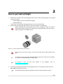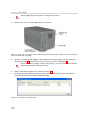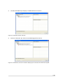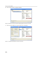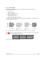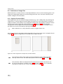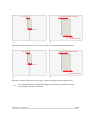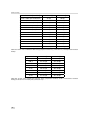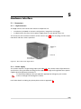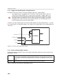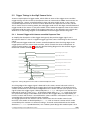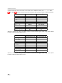
1
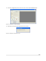
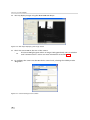
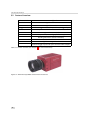
User Manual
MV1-D1312(I) Gigabit Ethernet Series
CMOS Area Scan Camera
MAN044 04/2009 V1.0
All information provided in this manual is believed to be accurate and reliable. No
responsibility is assumed by Photonfocus AG for its use. Photonfocus AG reserves the right to
make changes to this information without notice.
Reproduction of this manual in whole or in part, by any means, is prohibited without prior
permission having been obtained from Photonfocus AG.
1
2
Contents
1 Preface
1.1 About Photonfocus
1.2 Contact . . . . . . .
1.3 Sales Offices . . . .
1.4 Further information
1.5 Legend . . . . . . .
.
.
.
.
.
.
.
.
.
.
.
.
.
.
.
.
.
.
.
.
.
.
.
.
.
.
.
.
.
.
.
.
.
.
.
.
.
.
.
.
.
.
.
.
.
.
.
.
.
.
.
.
.
.
.
.
.
.
.
.
.
.
.
.
.
.
.
.
.
.
.
.
.
.
.
.
.
.
.
.
.
.
.
.
.
.
.
.
.
.
.
.
.
.
.
.
.
.
.
.
.
.
.
.
.
.
.
.
.
.
.
.
.
.
.
.
.
.
.
.
.
.
.
.
.
.
.
.
.
.
.
.
.
.
.
.
.
.
.
.
.
.
.
.
.
.
.
.
.
.
.
.
.
.
.
.
.
.
.
.
.
.
.
.
.
.
.
.
.
.
.
.
.
.
.
.
.
.
.
.
.
.
.
.
.
5
5
5
5
5
6
.
.
.
.
.
2 How to get started (GigE)
7
3 Product Specification
3.1 Introduction . . . . . . . . . . . . . . . . . . . . . . . . . . . . . . . . . . . . . . . . . .
3.2 Feature Overview . . . . . . . . . . . . . . . . . . . . . . . . . . . . . . . . . . . . . . .
3.3 Technical Specification . . . . . . . . . . . . . . . . . . . . . . . . . . . . . . . . . . . .
13
13
14
15
4 Functionality
4.1 Image Acquisition . . . . . . . . . . . . . . . . .
4.1.1 Free-running and Trigger Mode . . . . .
4.1.2 Exposure Control . . . . . . . . . . . . .
4.1.3 Maximum Frame Rate . . . . . . . . . .
4.2 Pixel Response . . . . . . . . . . . . . . . . . . .
4.2.1 Linear Response . . . . . . . . . . . . . .
4.2.2 LinLog® . . . . . . . . . . . . . . . . . . .
4.3 Image Correction . . . . . . . . . . . . . . . . .
4.3.1 Overview . . . . . . . . . . . . . . . . . .
4.3.2 Offset Correction (FPN, Hot Pixels) . . .
4.3.3 Gain Correction . . . . . . . . . . . . . .
4.3.4 Corrected Image . . . . . . . . . . . . . .
4.4 Reduction of Image Size . . . . . . . . . . . . .
4.4.1 Region of Interest (ROI) . . . . . . . . .
4.4.2 ROI configuration . . . . . . . . . . . . .
4.4.3 Calculation of the maximum frame rate
4.5 External Trigger . . . . . . . . . . . . . . . . . .
4.5.1 Trigger Source . . . . . . . . . . . . . . .
4.6 Strobe Output . . . . . . . . . . . . . . . . . . .
4.7 Convolver . . . . . . . . . . . . . . . . . . . . . .
4.7.1 Functionality . . . . . . . . . . . . . . . .
4.7.2 Settings . . . . . . . . . . . . . . . . . . .
.
.
.
.
.
.
.
.
.
.
.
.
.
.
.
.
.
.
.
.
.
.
.
.
.
.
.
.
.
.
.
.
.
.
.
.
.
.
.
.
.
.
.
.
.
.
.
.
.
.
.
.
.
.
.
.
.
.
.
.
.
.
.
.
.
.
.
.
.
.
.
.
.
.
.
.
.
.
.
.
.
.
.
.
.
.
.
.
.
.
.
.
.
.
.
.
.
.
.
.
.
.
.
.
.
.
.
.
.
.
.
.
.
.
.
.
.
.
.
.
.
.
.
.
.
.
.
.
.
.
.
.
.
.
.
.
.
.
.
.
.
.
.
.
.
.
.
.
.
.
.
.
.
.
.
.
.
.
.
.
.
.
.
.
.
.
.
.
.
.
.
.
.
.
.
.
.
.
.
.
.
.
.
.
.
.
.
.
.
.
.
.
.
.
.
.
.
.
.
.
.
.
.
.
.
.
.
.
.
.
.
.
.
.
.
.
.
.
.
.
.
.
.
.
.
.
.
.
.
.
.
.
.
.
.
.
.
.
.
.
.
.
.
.
.
.
.
.
.
.
.
.
.
.
.
.
.
.
.
.
.
.
.
.
.
.
.
.
.
.
.
.
.
.
.
.
.
.
.
.
.
.
.
.
.
.
.
.
.
.
.
.
.
.
.
.
.
.
.
.
.
.
.
.
.
.
.
.
.
.
.
.
.
.
.
.
.
.
.
.
.
.
.
.
.
.
.
.
.
.
.
.
.
.
.
.
.
.
.
.
.
.
.
.
.
.
.
.
.
.
.
.
.
.
.
.
.
.
.
.
.
.
.
.
.
.
.
.
.
.
.
.
.
.
.
.
.
.
.
.
.
.
.
.
.
.
.
.
.
.
.
.
.
.
.
.
.
.
.
.
.
.
.
.
.
.
.
.
.
.
.
.
.
.
.
.
.
.
.
.
.
.
.
.
.
.
.
.
.
.
.
.
.
.
.
.
.
.
.
.
19
19
19
21
21
21
21
22
26
26
27
29
31
32
32
35
35
37
37
37
38
38
38
5 Hardware Interface
5.1 Connectors . . . . . . . . . . . . . . . . . . . . . . . .
5.1.1 GigE Connector . . . . . . . . . . . . . . . . .
5.1.2 Power Supply . . . . . . . . . . . . . . . . . .
5.1.3 Trigger and Strobe Signals for GigE Cameras
.
.
.
.
.
.
.
.
.
.
.
.
.
.
.
.
.
.
.
.
.
.
.
.
.
.
.
.
.
.
.
.
.
.
.
.
.
.
.
.
.
.
.
.
.
.
.
.
.
.
.
.
.
.
.
.
.
.
.
.
.
.
.
.
.
.
.
.
.
.
.
.
.
.
.
.
39
39
39
39
40
CONTENTS
.
.
.
.
.
.
.
.
.
.
.
.
.
.
.
.
.
.
.
.
.
.
.
.
.
.
.
.
.
.
.
.
.
.
.
.
.
.
.
.
.
.
.
.
3
CONTENTS
5.1.4 Status Indicator (GigE cameras) . . . . . . . . . . . . . . . . . . . . . . . . . . . 40
5.2 Trigger Timings in the GigE Camera Series . . . . . . . . . . . . . . . . . . . . . . . . . 41
5.2.1 External Trigger with Camera controlled Exposure Time . . . . . . . . . . . . 41
6 Mechanical and Optical Considerations
6.1 Mechanical Interface . . . . . . . . .
6.1.1 Cameras with GigE Interface .
6.2 Optical Interface . . . . . . . . . . . .
6.2.1 Cleaning the Sensor . . . . . .
6.3 Compliance . . . . . . . . . . . . . . .
.
.
.
.
.
.
.
.
.
.
.
.
.
.
.
.
.
.
.
.
.
.
.
.
.
.
.
.
.
.
.
.
.
.
.
.
.
.
.
.
.
.
.
.
.
.
.
.
.
.
.
.
.
.
.
.
.
.
.
.
.
.
.
.
.
.
.
.
.
.
.
.
.
.
.
.
.
.
.
.
.
.
.
.
.
.
.
.
.
.
.
.
.
.
.
.
.
.
.
.
.
.
.
.
.
.
.
.
.
.
.
.
.
.
.
.
.
.
.
.
.
.
.
.
.
.
.
.
.
.
.
.
.
.
.
.
.
.
.
.
43
43
43
44
44
46
7 Warranty
47
7.1 Warranty Terms . . . . . . . . . . . . . . . . . . . . . . . . . . . . . . . . . . . . . . . . 47
7.2 Warranty Claim . . . . . . . . . . . . . . . . . . . . . . . . . . . . . . . . . . . . . . . . 47
8 References
49
A Pinouts
51
A.1 Power Supply Connector . . . . . . . . . . . . . . . . . . . . . . . . . . . . . . . . . . . 51
B Revision History
4
53
1
Preface
1.1
About Photonfocus
The Swiss company Photonfocus is one of the leading specialists in the development of CMOS
image sensors and corresponding industrial cameras for machine vision, security & surveillance
and automotive markets.
Photonfocus is dedicated to making the latest generation of CMOS technology commercially
available. Active Pixel Sensor (APS) and global shutter technologies enable high speed and
high dynamic range (120 dB) applications, while avoiding disadvantages like image lag,
blooming and smear.
Photonfocus has proven that the image quality of modern CMOS sensors is now appropriate
for demanding applications. Photonfocus’ product range is complemented by custom design
solutions in the area of camera electronics and CMOS image sensors.
Photonfocus is ISO 9001 certified. All products are produced with the latest techniques in order
to ensure the highest degree of quality.
1.2
Contact
Photonfocus AG, Bahnhofplatz 10, CH-8853 Lachen SZ, Switzerland
Sales
Phone: +41 55 451 07 45
Email: [email protected]
Support
Phone: +41 55 451 01 37
Email: [email protected]
Table 1.1: Photonfocus Contact
1.3
Sales Offices
Photonfocus products are available through an extensive international distribution network
and through our key account managers. Details of the distributor nearest you and contacts to
our key account managers can be found at www.photonfocus.com.
1.4
Further information
Photonfocus reserves the right to make changes to its products and documentation without notice. Photonfocus products are neither intended nor certified for
use in life support systems or in other critical systems. The use of Photonfocus
products in such applications is prohibited.
Photonfocus is a trademark and LinLog® is a registered trademark of Photonfocus AG. CameraLink® and GigE Vision® is a registered mark of the Automated
Imaging Association. Product and company names mentioned herein are trademarks or trade names of their respective companies.
5
1 Preface
Reproduction of this manual in whole or in part, by any means, is prohibited
without prior permission having been obtained from Photonfocus AG.
Photonfocus can not be held responsible for any technical or typographical errors.
1.5
Legend
In this documentation the reader’s attention is drawn to the following icons:
Important note
Alerts and additional information
Attention, critical warning
✎
6
Notification, user guide
2
How to get started (GigE)
1.
Remove the camera from its packaging. Please make sure the following items are included
with your camera:
•
Power supply connector (7-pole power plug)
•
Camera body cap
If any items are missing or damaged, please contact your dealership.
2.
Remove the camera body cap from the camera and mount a suitable lens.
When removing the camera body cap or when changing the lens, the camera
should always be held with the opening facing downwards to prevent dust or
debris falling onto the CMOS sensor.
Figure 2.1: Camera with protective cap and lens.
Do not touch the sensor surface. Protect the image sensor from particles and
dirt!
The sensor has no cover glass, therefore dust on the sensor surface may resemble
to clusters or extended regions of dead pixel.
To choose a lens, see
www.photonfocus.com.
3.
the
Lens
Finder
in
the
’Support’
area
at
To ensure maximum performance of the GigE camera it is mandatory to have the Intel
PRO/1000 PT installed in your PC.
Download the lastest driver installation tool from the Photonfocus server.
7
2 How to get started (GigE)
Do not apply Coyote software to configure the camera.
4.
Connect the camera to the GigE interface of your PC.
Figure 2.2: Rear view of the GigE camera MV1-D1312(I)-40-GB with power supply and I/O connector, Ethernet jack (RJ45) and status LED
5.
Connect a suitable power supply to the provided 7-pole power plug. For the connector
assembly see Fig. A.1. The pinout of the connector is shown in Appendix A.
Check the correct supply voltage and polarity! Do not exceed the maximum
operating voltage of +12V DC (± 10%).
6.
Connect the power supply to the camera (see Fig. 2.2).
7.
Download the latest driver installation tool from the Photonfocus server and start the
installation process of the eBus PureGEV package.
Figure 2.3: eBUS Driver Installation Tool
.
8
8.
The eBus PureGEV Player displays available Ethernet interfaces.
Figure 2.4: GEV Player Device Selection
9.
Camera is detected. Tip: Select unreachable GigE Vision Devices.
Figure 2.5: GEV Device Selection Procedure displaying the selected camera MV1-D1312(I)-GB
.
9
2 How to get started (GigE)
10. Select camera model to configure IP address.
Figure 2.6: GEV Device Selection Procedure displaying GigE Vision Device Information
11. Select a valid IP address for selected camera (e.g. 192.168.5.4).
Figure 2.7: Completing the GEV Device Selection Procedure
.
10
12. Finish the configuration process and connect the camera to eBus PURE GEV Player.
Figure 2.8: GEV Player is readily configured
13. GEV Player starts opening the eBUS stream to the camera.
Figure 2.9: GEV Player starting eBUS stream
.
11
2 How to get started (GigE)
14. You may display images using the eBUS PURE GEV Player.
Figure 2.10: GEV Player displaying live image stream
15. Check the status LED on the rear of the camera.
✎
The status LED lights green when an image is being produced, and it is red when
serial communication is active. For more information see Section 5.1.4.
16. To configure the camera use the GEV device control tool, selecting the visibility modus
"Beginner".
Figure 2.11: Control settings on the camera
12
3
Product Specification
3.1
Introduction
The MV1-D1312(I) CMOS camera series is built around the monochrome A1312(I) CMOS image
sensor from Photonfocus, that provides a resolution of 1312 x 1082 pixels at a wide range of
spectral sensitivity. It is aimed at standard applications in industrial image processing. The
principal advantages are:
•
Resolution of 1312 x 1082 pixels.
•
Wide spectral sensitivity from 320 nm to 1030 nm.
•
Enhanced near infrared (NIR) sensitivity with the A1312I CMOS image sensor.
•
High quantum efficiency (> 50%).
•
High pixel fill factor (> 60%).
•
Superiour signal-to-noise ratio (SNR).
•
Low power consumption at high speeds.
•
Very high resistance to blooming.
•
High dynamic range of up to 120 dB.
•
Ideal for high speed applications: Global shutter.
•
Greyscale resolution of up to 12 bit.
•
On camera shading correction.
•
3x3 Convolver included on camera.
•
Software provided for setting and storage of camera parameters.
•
The camera has a Gigabit Ethernet interface.
•
The compact size of (TBC) mm3 makes the MV1-D1312(I) CMOS cameras the perfect
solution for applications in which space is at a premium.
The general specification and features of the camera are listed in the following sections.
.
13
3 Product Specification
3.2
Feature Overview
Characteristics
MV1-D1312(I) Series
Interface
Gigabit Ethernet
Camera Control
GigE Vision Suite
Trigger Modes
Features
Interface Trigger / External opto isolated trigger input
Greyscale resolution 12 bit / 10 bit / 8 bit
Region of Interest (ROI)
Test pattern (LFSR and grey level ramp)
Shading Correction (Offset and Gain)
3x3 Convolver included on camera
High blooming resistance
isolated trigger input and opto isolated strobe output
Table 3.1: Feature overview (see Chapter 4 for more information)
Figure 3.1: MV1-D1312(I) CMOS camera with C-mount lens
.
14
3.3
Technical Specification
Technical Parameters
Technology
Scanning system
Optical format / diagonal
MV1-D1312(I) Series
CMOS active pixel (APS)
Progressive scan
1” (13.6 mm diagonal) @ maximum resolution
2/3” (11.6 mm diagonal) @ 1024 x 1024 resolution
Resolution
Pixel size
Active optical area
Random noise
1312 x 1082 pixels
8 µm x 8 µm
10.48 mm x 8.64 mm (maximum)
< 0.3 DN @ 8 bit 1)
Fixed pattern noise (FPN)
3.4 DN @ 8 bit / correction OFF 1)
Fixed pattern noise (FPN)
< 1DN @ 8 bit / correction ON 1)2)
Dark current MV1-D1312
0.65 fA / pixel @ 27 °C
Dark current MV1-D1312I
0.79 fA / pixel @ 27 °C
Full well capacity
~ 100 ke−
Spectral range MV1-D1312
350 nm ... 980 nm (see Fig. 3.2)
Spectral range MV1-D1312I
350 nm ... 1100 nm (see Fig. 3.3)
Responsivity MV1-D1312
295 x103 DN/(J/m2 ) @ 670 nm / 8 bit
Responsivity MV1-D1312I
305 x103 DN/(J/m2 ) @ 850 nm / 8 bit
Quantum Efficiency
Optical fill factor
50 % @ max.
60 %
Dynamic range
60 dB in linear mode, 120 dB with LinLog®
Colour format
Monochrome
Characteristic curve
Linear, LinLog®
Shutter mode
Global shutter
Greyscale resolution
12 bit / 10 bit / 8 bit
Table 3.2: General specification of the MV1-D1312(I) CMOS camera series (Footnotes:
are typical values. 2) Indicated values are subject to confirmation.)
3.3 Technical Specification
1)
Indicated values
15
3 Product Specification
MV1-D1312(I)-40
MV1-D1312(I)-80
10 µs ... 1.68 s
10 µs ... 1.68 s
100 ns
50 ns
27 fps @ 8 bit
54 fps @ 8 bit
40 MHz
40 MHz
25 ns
25 ns
Exposure Time
Exposure time increment
3)
Frame rate
( Tint = 10 µs)
Pixel clock frequency
Pixel clock cycle
Read out mode
Table 3.3: Model-specific parameters (Footnote:
sequential or simultaneous
3)
Maximum frame rate @ full resolution @ 8 bit)
MV1-D1312(I)-40
Operating temperature
Camera power supply
Trigger signal input range
Max. power consumption
MV1-D1312(I)-80
0°C ... 50°C
+12 V DC (± 10 %)
+5 .. +15 V DC
< 2.5 W (TBD)
< 3.0 W (TBD)
Lens mount
C-Mount (CS-Mount optional)
Dimensions
60 x 60 x 94 mm3
Mass
Conformity
480 g
CE / RoHS / WEE
Table 3.4: Physical characteristics and operating ranges of the MV1-D1312(I) CMOS camera series
.
16
Fig. 3.2 shows the quantum efficiency and the responsivity of the A1312 CMOS sensor,
displayed as a function of wavelength. For more information on photometric and radiometric
measurements see the Photonfocus application notes AN006 and AN008 available in the
support area of our website at www.photonfocus.com.
60%
QE
1200
Responsivity
50%
1000
800
30%
600
20%
Responsivity [V
V/J/m²]
Quantum
m Efficiency
40%
400
10%
200
0%
200
0
300
400
500
600
700
800
900
1000
1100
Wavelength [nm]
Figure 3.2: Spectral response of the A1312 CMOS image sensor (standard) in the MV1-D1312 camera series
(Hint: the red-shifted curve corresponds to the responsivity curve.)
3.3 Technical Specification
17
3 Product Specification
Fig. 3.3 shows the quantum efficiency and the responsivity of the A1312I CMOS sensor,
displayed as a function of wavelength.
60%
QE
Responsivity
1200
50%
1000
800
30%
600
20%
Responsivity [V
V/J/m²]
Quantum
m Efficiency
40%
400
10%
200
0%
200
0
300
400
500
600
700
800
900
1000
1100
Wavelength [nm]
Figure 3.3: Spectral response of the A1312I image sensor (NIR enhanced) in the MV1-D1312I camera series
(Hint: the red-shifted curve corresponds to the responsivity curve.)
.
18
4
Functionality
This chapter serves as an overview of the camera configuration modes and explains camera
features. The goal is to describe what can be done with the camera. The setup of the
MV1-D1312(I) series cameras is explained in later chapters.
4.1
4.1.1
Image Acquisition
Free-running and Trigger Mode
The MV1-D1312(I) CMOS cameras provide two different readout modes:
Sequential readout Frame time is the sum of exposure time and readout time. Exposure time
of the next image can only start if the readout time of the current image is finished.
Simultaneous readout (interleave) The frame time is determined by the maximum of the
exposure time or of the readout time, which ever of both is the longer one. Exposure
time of the next image can start during the readout time of the current image.
MV1-D1312(I) Series
Sequential readout
available
Simultaneous readout
available
Table 4.1: Readout mode of MV1-D1312 Series camera
The following figure illustrates the effect on the frame rate when using either the sequential
readout mode or the simultaneous readout mode (interleave exposure).
fp s = 1 /r e a d o u t tim e
F ra m e ra te
(fp s)
S im u lta n e o u s
re a d o u t m o d e
fp s = 1 /e x p o s u r e tim e
S e q u e n tia l
re a d o u t m o d e
fp s = 1 /( r e a d o u t tim e + e x p o s u r e tim e )
e x p o s u re tim e < re a d o u t tim e
e x p o s u re tim e = re a d o u t tim e
e x p o s u re tim e > re a d o u t tim e
E x p o s u re tim e
Figure 4.1: Frame rate in sequential readout mode and simultaneous readout mode
Sequential readout mode For the calculation of the frame rate only a single formula applies:
frames per second equal to the inverse of the sum of exposure time and readout time.
19
4 Functionality
Simultaneous readout mode (exposure time < readout time) The frame rate is given by the
readout time. Frames per second equal to the inverse of the readout time.
Simultaneous readout mode (exposure time > readout time) The frame rate is given by the
exposure time. Frames per second equal to the inverse of the exposure time.
The simultaneous readout mode allows higher frame rate. However, if the exposure time
greatly exceeds the readout time, then the effect on the frame rate is neglectable.
In simultaneous readout mode image output faces minor limitations. The overall
linear sensor reponse is partially restricted in the lower grey scale region.
When changing readout mode from sequential to simultaneous readout mode
or vice versa, new settings of the BlackLevelOffset and of the image correction
are required.
Sequential readout
By default the camera continuously delivers images as fast as possible ("Free-running mode")
in the sequential readout mode. Exposure time of the next image can only start if the readout
time of the current image is finished.
e x p o s u re
re a d o u t
e x p o s u re
re a d o u t
Figure 4.2: Timing in free-running sequential readout mode
When the acquisition of an image needs to be synchronised to an external event, an external
trigger can be used (refer to Section 4.5 and to Section 5.2). In this mode, the camera is idle
until it gets a signal to capture an image.
e x p o s u re
re a d o u t
id le
e x p o s u re
e x te r n a l tr ig g e r
Figure 4.3: Timing in triggered sequential readout mode
Simultaneous readout (interleave exposure)
To achieve highest possible frame rates, the camera must be set to "Free-running mode" with
simultaneous readout. The camera continuously delivers images as fast as possible. Exposure
time of the next image can start during the readout time of the current image.
e x p o s u re n
re a d o u t n -1
id le
e x p o s u re n + 1
re a d o u t n
id le
re a d o u t n + 1
fr a m e tim e
Figure 4.4: Timing in free-running simultaneous readout mode (readout time> exposure time)
20
e x p o s u re n -1
id le
e x p o s u re n + 1
e x p o s u re n
re a d o u t n -1
id le
re a d o u t n
fr a m e tim e
Figure 4.5: Timing in free-running simultaneous readout mode (readout time< exposure time)
When the acquisition of an image needs to be synchronised to an external event, an external
trigger can be used (refer to Section 4.5 and to Section 5.2). In this mode, the camera is idle
until it gets a signal to capture an image.
Figure 4.6: Timing in triggered simultaneous readout mode
4.1.2
Exposure Control
The exposure time defines the period during which the image sensor integrates the incoming
light. Refer to Table 3.3 for the allowed exposure time range.
4.1.3
Maximum Frame Rate
The maximum frame rate depends on the exposure time and the size of the image (see Section
4.4.)
4.2
4.2.1
Pixel Response
Linear Response
The camera offers a linear response between input light signal and output grey level. This can
be modified by the use of LinLog® as described in the following sections. In addition, a linear
digital gain may be applied, as follows. Please see Table 3.2 for more model-dependent
information.
Gain x1, x2, x4
Gain x1, x2 and x4 are digital amplifications, which means that the digital image data are
multiplied in the camera by a factor 1, 2 or 4, respectively.
4.2 Pixel Response
21
4 Functionality
Black Level Adjustment
The black level is the average image value at no light intensity. It can be adjusted by the
software by changing the black level offset. Thus, the overall image gets brighter or darker.
Use a histogram to control the settings of the black level.
4.2.2
LinLog®
Overview
The LinLog® technology from Photonfocus allows a logarithmic compression of high light
intensities inside the pixel. In contrast to the classical non-integrating logarithmic pixel, the
LinLog® pixel is an integrating pixel with global shutter and the possibility to control the
transition between linear and logarithmic mode.
In situations involving high intrascene contrast, a compression of the upper grey level region
can be achieved with the LinLog® technology. At low intensities each pixel shows a linear
response. At high intensities the response changes to logarithmic compression (see Fig. 4.7).
The transition region between linear and logarithmic response can be smoothly adjusted by
software and is continuously differentiable and monotonic.
G re y
V a lu e
S a tu r a tio n
1 0 0 %
L in e a r
R e s p o n s e
W e a k c o m p r e s s io n
R e s u ltin g L in lo g
R e s p o n s e
S tr o n g c o m p r e s s io n
0 %
V a lu e 1
V a lu e 2
L ig h t In te n s ity
Figure 4.7: Resulting LinLog2 response curve
LinLog® is controlled by up to 4 parameters (Time1, Time2, Value1 and Value2). Value1 and Value2
correspond to the LinLog® voltage that is applied to the sensor. The higher the parameters
Value1 and Value2 respectively, the stronger the compression for the high light intensities. Time1
and Time2 are normalised to the exposure time. They can be set to a maximum value of 1000,
which corresponds to the exposure time.
Examples in the following sections illustrate the LinLog® feature.
LinLog1
In the simplest way the pixels are operated with a constant LinLog® voltage which defines the
knee point of the transition.This procedure has the drawback that the linear response curve
changes directly to a logarithmic curve leading to a poor grey resolution in the logarithmic
region (see Fig. 4.9).
22
V
L in L o g
t
e x p
V a lu e 1
= V a lu e 2
T im e 1 = T im e 2 = m a x .
= 1 0 0 0
0
t
Figure 4.8: Constant LinLog voltage in the Linlog1 mode
Typical LinLog1 Response Curve − Varying Parameter Value1
Time1=1000, Time2=1000, Value2=Value1
300
Output grey level (8 bit) [DN]
250
V1 = 15
V1 = 16
V1 = 17
200
V1 = 18
V1 = 19
150
100
50
0
Illumination Intensity
Figure 4.9: Response curve for different LinLog settings in LinLog1 mode
.
4.2 Pixel Response
23
4 Functionality
LinLog2
To get more grey resolution in the LinLog® mode, the LinLog2 procedure was developed. In
LinLog2 mode a switching between two different logarithmic compressions occurs during the
exposure time (see Fig. 4.10). The exposure starts with strong compression with a high
LinLog® voltage (Value1). At Time1 the LinLog® voltage is switched to a lower voltage resulting in
a weaker compression. This procedure gives a LinLog® response curve with more grey
resolution. Fig. 4.11 and Fig. 4.12 show how the response curve is controlled by the three
parameters Value1, Value2 and the LinLog® time Time1.
Settings in LinLog2 mode, enable a fine tuning of the slope in the logarithmic
region.
V
L in L o g
t
e x p
V a lu e 1
V a lu e 2
T im e 1
0
T im e 1
T im e 2 = m a x .
= 1 0 0 0
t
Figure 4.10: Voltage switching in the Linlog2 mode
Typical LinLog2 Response Curve − Varying Parameter Time1
Time2=1000, Value1=19, Value2=14
300
T1 = 840
Output grey level (8 bit) [DN]
250
T1 = 920
T1 = 960
200
T1 = 980
T1 = 999
150
100
50
0
Illumination Intensity
Figure 4.11: Response curve for different LinLog settings in LinLog2 mode
24
Typical LinLog2 Response Curve − Varying Parameter Time1
Time2=1000, Value1=19, Value2=18
200
Output grey level (8 bit) [DN]
180
160
140
120
T1 = 880
T1 = 900
T1 = 920
T1 = 940
T1 = 960
T1 = 980
T1 = 1000
100
80
60
40
20
0
Illumination Intensity
Figure 4.12: Response curve for different LinLog settings in LinLog2 mode
LinLog3
To enable more flexibility the LinLog3 mode with 4 parameters was introduced. Fig. 4.13 shows
the timing diagram for the LinLog3 mode and the control parameters.
V
L in L o g
t
e x p
V a lu e 1
V a lu e 2
T im e 1
V a lu e 3 = C o n s ta n t = 0
T im e 2
T im e 1
T im e 2
t
t
e x p
Figure 4.13: Voltage switching in the LinLog3 mode
4.2 Pixel Response
25
4 Functionality
Typical LinLog2 Response Curve − Varying Parameter Time2
Time1=850, Value1=19, Value2=18
300
T2 = 950
T2 = 960
T2 = 970
T2 = 980
T2 = 990
Output grey level (8 bit) [DN]
250
200
150
100
50
0
Illumination Intensity
Figure 4.14: Response curve for different LinLog settings in LinLog3 mode
4.3
4.3.1
Image Correction
Overview
The camera possesses image pre-processing features, that compensate for non-uniformities
caused by the sensor, the lens or the illumination. This method of improving the image quality
is generally known as ’Shading Correction’ or ’Flat Field Correction’ and consists of a
combination of offset correction, gain correction and pixel interpolation.
Since the correction is performed in hardware, there is no performance limitation of the cameras for high frame rates.
The offset correction subtracts a configurable positive or negative value from the live image
and thus reduces the fixed pattern noise of the CMOS sensor. In addition, hot pixels can be
removed by interpolation. The gain correction can be used to flatten uneven illumination or to
compensate shading effects of a lens. Both offset and gain correction work on a pixel-per-pixel
basis, i.e. every pixel is corrected separately. For the correction, a black reference and a grey
reference image are required. Then, the correction values are determined automatically in the
camera.
Do not set any reference images when gain or LUT is enabled! Read the following sections very carefully.
Correction values of both reference images can be saved into the internal flash memory, but
this overwrites the factory presets. Then the reference images that are delivered by factory
cannot be restored anymore.
26
4.3.2
Offset Correction (FPN, Hot Pixels)
The offset correction is based on a black reference image, which is taken at no illumination
(e.g. lens aperture completely closed). The black reference image contains the fixed-pattern
noise of the sensor, which can be subtracted from the live images in order to minimise the
static noise.
Offset correction algorithm
After configuring the camera with a black reference image, the camera is ready to apply the
offset correction:
1.
Determine the average value of the black reference image.
2.
Subtract the black reference image from the average value.
3.
Mark pixels that have a grey level higher than 252 DN (@ 10 bit) as hot pixels.
4.
Store the result in the camera as the offset correction matrix.
5.
During image acquisition, subtract the correction matrix from the acquired image and
interpolate the hot pixels (see Section 4.3.2).
4.3 Image Correction
27
4 Functionality
1
4
3
1
4
4
4
2
1
2
4
4
3
2
3
1
1
1
3
4
3
1
3
4
4
-
b la c k r e fe r e n c e
im a g e
a v e ra
o f b la
re fe re
p ic tu
g e
c k
n c e
re
=
1
1
1
-2
1
1
-1
2
-1
1
-1
1
2
0
-2
0
0
-1
-1
0
2
-2
0
-2
-2
o ffs e t c o r r e c tio n
m a tr ix
Figure 4.15: Schematic presentation of the offset correction algorithm
How to Obtain a Black Reference Image
In order to improve the image quality, the black reference image must meet certain demands.
•
The black reference image must be obtained at no illumination, e.g. with lens aperture
closed or closed lens opening.
•
It may be necessary to adjust the black level offset of the camera. In the histogram of the
black reference image, ideally there are no grey levels at value 0 DN after adjustment of
the black level offset. All pixels that are saturated black (0 DN) will not be properly
corrected (see Fig. 4.16). The peak in the histogram should be well below the hot pixel
threshold of 252 DN @ 10 bit.
•
Camera settings may influence the grey level. Therefore, for best results the camera
settings of the black reference image must be identical with the camera settings of the
image to be corrected.
Figure 4.16: Histogram of a proper black reference image for offset correction
Hot pixel correction
Every pixel that exceeds a certain threshold in the black reference image is marked as a hot
pixel. If the hot pixel correction is switched on, the camera replaces the value of a hot pixel by
an average of its neighbour pixels (see Fig. 4.17).
28
p
h o t
p ix e l
n -1
p
n
p
p
n
=
p
n -1
+ p
2
n + 1
n + 1
Figure 4.17: Hot pixel interpolation
4.3.3
Gain Correction
The gain correction is based on a grey reference image, which is taken at uniform illumination
to give an image with a mid grey level.
Gain correction is not a trivial feature. The quality of the grey reference image
is crucial for proper gain correction.
Gain correction algorithm
After configuring the camera with a black and grey reference image, the camera is ready to
apply the gain correction:
1.
Determine the average value of the grey reference image.
2.
Subtract the offset correction matrix from the grey reference image.
3.
Divide the average value by the offset corrected grey reference image.
4.
Pixels that have a grey level higher than a certain threshold are marked as hot pixels.
5.
Store the result in the camera as the gain correction matrix.
6.
During image acquisition, multiply the gain correction matrix from the offset-corrected
acquired image and interpolate the hot pixels (see Section 4.3.2).
Gain correction is not a trivial feature. The quality of the grey reference image
is crucial for proper gain correction.
4.3 Image Correction
29
4 Functionality
a v e
o f
re fe
p ic
ra
g r
re
tu
g e
a y
n c e
re
:
1
4
3
1
7
4
4
8
2
9
9
7
6
7
9
3
7
1 0
9
8
3
1 0
4
6
1
g ra y re fe re n c e
p ic tu r e
-
1
1
1
-2
1
1
-1
2
-1
1
-1
1
2
0
-2
0
0
-1
-1
0
2
-2
0
-2
-2
o ffs e t c o r r e c tio n
m a tr ix
)
=
1
1
1
0 .9
-2
1 .2
1
1
1
0 .9
0
-1
1
1
1 .2 0 .8
1
-2
1
-2
0
0 .8
1 .3
1
-2
g a in c o r r e c tio n
m a tr ix
Figure 4.18: Schematic presentation of the gain correction algorithm
Gain correction always needs an offset correction matrix. Thus, the offset correction always has to be performed before the gain correction.
How to Obtain a Grey Reference Image
In order to improve the image quality, the grey reference image must meet certain demands.
•
The grey reference image must be obtained at uniform illumination.
Use a high quality light source that delivers uniform illumination. Standard illumination will not be appropriate.
•
When looking at the histogram of the grey reference image, ideally there are no grey
levels at full scale (1023 DN @ 10 bit). All pixels that are saturated white will not be
properly corrected (see Fig. 4.19).
•
Camera settings may influence the grey level. Therefore, the camera settings of the grey
reference image must be identical with the camera settings of the image to be corrected.
Figure 4.19: Proper grey reference image for gain correction
30
4.3.4
Corrected Image
Offset, gain and hot pixel correction can be switched on separately. The following
configurations are possible:
•
No correction
•
Offset correction only
•
Offset and hot pixel correction
•
Hot pixel correction only
•
Offset and gain correction
•
Offset, gain and hot pixel correction
)
In addition, the black reference image and grey reference image that are currently stored in
the camera RAM can be output.
1
4
3
7
4
5
4
7
6
7
6
4
5
6
3
7
6
6
5
3
7
1
c u r r e n t im a g e
4
3
4
-
1
1
1
-2
1
1
-1
2
-1
1
-1
0
1
-1
2
0
-2
0
0
0
-1
-2
2
-2
-2
o ffs e t c o r r e c tio n
m a tr ix
.
1
1
1
0 .9
-2
1 .2
1
1
1
0 .9
0
-1
1
1
1 .2 0 .8
1
-2
1
1
4
0
-2
0 .8
1 .3
1
=
-2
g a in c o r r e c tio n
m a tr ix
3
7
5
4
4
7
5
7
6
4
5
6
3
5
6
4
5
3
6
1
3
4
4
c o r r e c te d im a g e
Figure 4.20: Schematic presentation of the corrected image using gain correction algorithm
Table 4.2 shows the minimum and maximum values of the correction matrices, i.e. the range
that the offset and gain algorithm can correct.
Offset correction
Minimum
Maximum
-127 DN @ 10 bit
+127 DN @ 10 bit
0.42
2.67
Gain correction
Table 4.2: Offset and gain correction ranges
4.3 Image Correction
31
4 Functionality
4.4
Reduction of Image Size
With Photonfocus cameras there are several possibilities to focus on the interesting parts of an
image, thus reducing the data rate and increasing the frame rate. The most commonly used
feature is Region of Interest (ROI).
4.4.1
Region of Interest (ROI)
Some applications do not need full image resolution (e.g. 1312 x 1082 pixels). By reducing the
image size to a certain region of interest (ROI), the frame rate can be drastically increased. A
region of interest can be almost any rectangular window and is specified by its position within
the full frame and its width (W) and height (H). Fig. 4.22 and Fig. 4.23 shows possible
configurations for the region of interest, and Table 4.3 presents numerical examples of how
the frame rate can be increased by reducing the ROI.
Both reductions in x- and y-direction result in a higher frame rate.
Any region of interest may NOT be placed outside of the center of the sensor. Examples shown
in Fig. 4.21 illustrate configurations of the ROI that are NOT allowed.
a )
b )
Figure 4.21: ROI configuration examples that are NOT allowed
The minimum width of the region of interest depends on the model of the MV1D1312(I) camera series. For more details please consult Table 4.5 and Table 4.6.
The minimum width must be positioned symmetrically towards the vertical center line of the sensor as shown in Fig. 4.22 and Fig. 4.23). A list of possible
settings of the ROI for each camera model is given in Table 4.6.
.
32
³ 1 4 4 P ix e l
³ 1 4 4 P ix e l + m o d u lo 3 2 P ix e l
³ 1 4 4 P ix e l
³ 1 4 4 P ix e l
+ m o d u lo 3 2 P ix e l
b )
a )
Figure 4.22: Possible configuration of the region of interest for the MV1-D1312(I)-40 CMOS camera
³ 2 0 8 P ix e l
³ 2 0 8 P ix e l + m o d u lo 3 2 P ix e l
³ 2 0 8 P ix e l
³ 2 0 8 P ix e l
+ m o d u lo 3 2 P ix e l
b )
a )
Figure 4.23: Possible configuration of the region of interest with MV1-D1312(I)-80 CMOS camera
✎
It is recommended to re-adjust the settings of the shading correction each time
a new region of interest is selected.
4.4 Reduction of Image Size
33
4 Functionality
ROI Dimension [Standard]
MV1-D1312(I)-40
MV1-D1312(I)-80
1312 x 1082 (full resolution)
27 fps
54 fps
288 x 1 (minimum resolution)
10245 fps
10863 fps
1280 x 1024 (SXGA)
29 fps
58 fps
1280 x 768 (WXGA)
39 fps
78 fps
800 x 600 (SVGA)
79 fps
157 fps
640 x 480 (VGA)
121 fps
241 fps
544 x 1
9615 fps
10498 fps
544 x 1082
63 fps
125 fps
1312 x 544
54 fps
107 fps
1312 x 256
114 fps
227 fps
544 x 544
125 fps
248 fps
1024 x 1024
36 fps
72 fps
1312 x 1
8116 fps
9537 fps
Table 4.3: Frame rates of different ROI settings (exposure time 10 µs; correction on, and sequential readout
mode).
Exposure time
MV1-D1312(I)-40
MV1-D1312(I)-80
10 µs
27 / 27 fps
54 / 54 fps
100 µs
27 / 27 fps
54 / 54 fps
500 µs
27 / 27 fps
53 / 54 fps
1 ms
27 / 27 fps
51 / 54 fps
2 ms
26 / 27 fps
49 / 54 fps
5 ms
24 / 27 fps
42 / 54 fps
10 ms
22 / 27 fps
35 / 54 fps
12 ms
21 / 27 fps
33 / 54 fps
Table 4.4: Frame rates of different exposure times, [sequential readout mode / simultaneous readout
mode], resolution 1312 x 1082 pixel (correction on).
.
34
4.4.2
ROI configuration
In the MV1-D1312(I) camera series the following two restrictions have to be respected for the
ROI configuration:
•
The minimum width (w) of the ROI is camera model dependent, consisting of 288 pixel in
the MV1-D1312(I)-40 camera and of 416 pixel in the MV1-D1312(I)-80 camera.
•
The region of interest must overlap a minimum number of pixels centered to the left and
to the right of the vertical middle line of the sensor (ovl).
For any camera model of the MV1-D1312(I) camera series the allowed ranges for the ROI
settings can be deduced by the following formula:
xmin = max(0, 656 + ovl − w)
xmax = min(656 − ovl, 1312 − w)
.
where "ovl" is the overlap over the middle line and "w" is the width of the region of interest.
Any ROI settings exceeding the minimum ROI width must be modulo 32.
ROI width (w)
overlap (ovl)
width condition
MV1-D1312(I)-40
MV1-D1312(I)-80
288 ... 1312
416 ... 1312
144
208
modulo 32
modulo 32
Table 4.5: Summary of the ROI configuration restrictions for the MV1-D1312(I) camera series indicating the
minimum ROI width (w) and the required number of pixel overlap (ovl) over the sensor middle line
The settings of the region of interest in x-direction are restricted to modulo 32
(see Table 4.6).
There are no restrictions for the settings of the region of interest in y-direction.
4.4.3
Calculation of the maximum frame rate
The frame rate mainly depends on the exposure time and readout time. The frame rate is the
inverse of the frame time.
1
fps = tframe
Calculation of the frame time (sequential mode)
tframe ≥ texp + tro
Calculation of the frame time (simultaneous mode)
4.4 Reduction of Image Size
35
4 Functionality
Width
ROI-X (MV1-D1312(I)-40)
ROI-X (MV1-D1312(I)-80)
288
512
not available
320
480 ... 512
not available
352
448 ... 512
not available
384
416 ... 512
not available
416
384 ... 512
448
448
352 ... 512
416 ... 448
480
320 ... 520
384 ... 448
512
288 ... 512
352 ... 448
544
256 ...512
320 ... 448
576
224 ... 512
288 ... 448
608
192 ... 512
256 ... 448
640
160 ... 512
224 ... 448
672
128 ... 512
192 ... 448
704
96 ... 512
160 ... 448
736
64 ... 512
128 ... 448
768
32 ... 512
96 ... 448
800
0 ... 512
64 ... 448
832
0 ... 480
32 ... 448
864
0 ... 448
0 ... 448
896
0 ... 416
0 ... 416
...
...
...
1312
0
0
Table 4.6: Some possible ROI-X settings
The calculation of the frame time in simultaneous read out mode requires more detailed data
input and is skipped here for the purpose of clarity.
✎
The formula for the calculation of the frame time in simultaneous mode is available from Photonfocus on request.
ROI Dimension
MV1-D1312(I)-40
MV1-D1312(I)-80
1312 x 1082
tro = 36.46 ms
tro = 18.23 ms
1024 x 512
tro = 13.57 ms
tro = 6.78 ms
1024 x 256
tro = 6.78 ms
tro = 3.39 ms
Table 4.7: Read out time at different ROI settings for the MV1-D1312(I) CMOS camera series in sequential
read out mode.
36
A frame rate calculator for calculating the maximum frame rate is available in
the support area of the Photonfocus website.
4.5
External Trigger
An external trigger is an event that starts an exposure. The trigger signal is either generated by
the PC (soft-trigger) or comes from an external device such as a light barrier. If a trigger signal
is applied to the camera before the earliest time for the next trigger, this trigger will be
ignored.
4.5.1
Trigger Source
The trigger signal can be configured to be active high or active low.
Trigger In the trigger mode, the trigger signal is applied directly to the camera by the power
supply connector (via an optocoupler).
Figure 4.24: Trigger Inputs - Single GigE solution
4.6
Strobe Output
The strobe output is an opto-isolated output located on the power supply connector that can
be used to trigger a strobe. The strobe output can be used both in free-running and in trigger
mode. There is a programmable delay available to adjust the strobe pulse to your application.
The strobe output needs a separate power supply. Please see Section 5.2 and
Figure Fig. 4.24 and Fig. 4.25 for more information.
4.5 External Trigger
37
4 Functionality
Figure 4.25: Trigger Inputs - Multiple GigE solution
4.7
4.7.1
Convolver
Functionality
The "Convolver" is a discrete 2D-convolution filter with a 3x3 convolution kernel. The kernel
coefficients can be user-defined.
The M x N discrete 2D-convolution pout (x,y) of pixel pin (x,y) with convolution kernel h, scale s
and offset o is defined in Fig. 4.26.
Figure 4.26: Convolution formula
4.7.2
Settings
The following settings for the parameters are available:
Offset Offset value o (see Fig. 4.26). Range: -4096 ... 4095
Scale Scaling divisor s (see Fig. 4.26). Range: 1 ... 4095
Coefficients Coefficients of convolution kernel h (see Fig. 4.26). Range: -4096 ... 4095.
Assignment to coefficient properties is shown in Fig. 4.27.
Figure 4.27: Convolution coefficients assignment
38
5
Hardware Interface
5.1
Connectors
5.1.1
GigE Connector
The GigE cameras are interfaced to external components via
•
an Ethernet jack (RJ45) to transmit configuration, image data and trigger.
•
a subminiature connector for the power supply, 8-pin or 7-pin Binder series 712.
The connectors are located on the back of the camera. Fig. 5.1 shows the plugs and the status
LED which indicates camera operation.
Figure 5.1: Rear view of the GigE camera
5.1.2
Power Supply
The camera requires a single voltage input (see Table 3.4). The camera meets all performance
specifications using standard switching power supplies, although well-regulated linear power
supplies provide optimum performance.
It is extremely important that you apply the appropriate voltages to your camera.
Incorrect voltages will damage the camera.
For further details including the pinout please refer to Appendix A.
.
39
5 Hardware Interface
5.1.3
Trigger and Strobe Signals for GigE Cameras
The power connector contains an external trigger input and a strobe output.
The trigger input is equipped with a constant current diode which limits the
current of the optocoupler over a wide range of voltages. Trigger signals can
thus directly get connected with the input pin and there is no need for a current
limiting resistor, that depends with its value on the input voltage. The input
voltage to the TRIGGER pin must not exceed +15V DC, to avoid damage to the
internal ESD protection and the optocoupler!
In order to use the strobe output, the internal optocoupler must be powered with 5 .. 15 V DC.
The STROBE signal is an OP Amp’s output. The range of the output signal can be adjusted by the
STROBE-VDD.
I S O _ V D D
T R I G G E R
5 ... 1 5 V
D C
S T R O B E - V D D
5 ... 1 5 V
D C
S T R O B E
I n p u t
I s o la t o r
O u tp u t
S G N D
Figure 5.2: Circuit for the trigger input signals
5.1.4
Status Indicator (GigE cameras)
A dual-color LED on the back of the camera gives information about the current status of the
GigE CMOS cameras.
LED Green
Green when an image is output. At slow frame rates, the LED blinks with the
FVAL signal. At high frame rates the LED changes to an apparently continuous
green light, with intensity proportional to the ratio of readout time over frame
time.
LED Red
Red indicates an active serial communication with the camera.
Table 5.1: Meaning of the LED of the GigE CMOS cameras
.
40
5.2
Trigger Timings in the GigE Camera Series
There are 3 principles of trigger modes, which differ in terms of the trigger source and the
trigger timing. For the control of the exposure time of a Photonfocus CMOS camera there are
two possibilities: camera controlled exposure time and pulse width control. In the camera
controlled exposure mode an internal counter determines the exposure time of the camera.
This is used in the free running mode, the softtrigger mode and in the edge controlled external
trigger mode of the camera. In the pulse width control mode the exposure time of the camera
is determined by the pulse width of the trigger input pulse. In the following two sections the
differences in the timing diagram and a definition of the timing parameters are given.
5.2.1
External Trigger with Camera controlled Exposure Time
To simplify the description of the trigger timings only the positive trigger signal case is
discussed in detail. In case of a negative trigger signal the same is following for the inverted
signal.
In the external trigger mode with camera controlled exposure time the rising edge of the
trigger pulse starts the camera states machine, which controls the sensor and optional an
external strobe output. Fig. 5.3 shows the detailed timing diagram for the external trigger
mode with camera controlled exposure time.
e x t e r n a l t r ig g e r p u ls e in p u t
t
t r ig g e r a f t e r is o la t o r
t
d _ is o _ in p u t
t r ig g e r p u ls e in t e r n a l c a m e r a c o n t r o l
jit t e r
t
d e la y e d t r ig g e r f o r s h u t t e r c o n t r o l
t r ig g e r _ d e la y
t
e x p o s u r e
in t e r n a l s h u t t e r c o n t r o l
d e la y e d t r ig g e r f o r s t r o b e c o n t r o l
t
t
s t r o b e _ d e la y
s t r o b e d u r a t io n
t
d _ is o _ o u t p u t
in t e r n a l s t r o b e c o n t r o l
e x t e r n a l s t r o b e p u ls e o u t p u t
Figure 5.3: Timing diagram for the camera controlled exposure time
The rising edge of the trigger signal is detected in the camera control electronic which is
implemented in an FPGA. Before the trigger signal reaches the FPGA it is isolated from the
camera environment to allow robust integration of the camera into the vision system. In the
signal isolator the trigger signal is delayed by time td−iso−input . This signal is clocked into the
FPGA which leads to a jitter of tjitter . A minimum trigger delay ttrigger−delay results then from
the synchronous design of the FPGA state machines. This trigger delay can expanded by an
internal counter which value is user defined via camera software. The exposure time texposure is
controlled with an internal exposure time controller.
The trigger pulse from the internal camera control starts also the strobe control state
machines. The strobe can be delayed by tstrobe−delay with an internal counter which can be
controlled by the customer via software settings. A second counter determines the strobe
duration tstrobe−duration (strobe-duration). For a robust system design the strobe output is also
5.2 Trigger Timings in the GigE Camera Series
41
5 Hardware Interface
isolated from the camera electronic which leads to an additional delay of td−iso−output . Table
5.2 and Table 5.3 gives an overview over the minimum and maximum values of the parameters.
MV1-D1312(I)-40-GB
MV1-D1312(I)-40-GB
Minimum
Maximum
45 ns
60 ns
0
100 ns
ttrigger−delay
600 ns
user defined
texposure
10 µs
1.68 s
tstrobe−delay
600 ns
user defined
tstrobe−duration
200 ns
user defined
td−iso−output
45 ns
60 ns
ttrigger−pulsewidth
40 ns
n/a
Timing Parameter
td−iso−input
tjitter
Table 5.2: Summary of timing parameters relevant in the external trigger mode using camera (MV1D1312(I)-40-GB) controlled exposure time
MV1-D1312(I)-80-GB
MV1-D1312(I)-80-GB
Timing Parameter
Minimum
Maximum
td−iso−input
45 ns
60 ns
tjitter
0
50 ns
ttrigger−delay
300 ns
user defined
texposure
10 µs
1.68 s
tstrobe−delay
300 ns
user defined
tstrobe−duration
100 ns
user defined
td−iso−output
45 ns
60 ns
ttrigger−pulsewidth
40 ns
n/a
Table 5.3: Summary of timing parameters relevant in the external trigger mode using camera (MV1D1312(I)-80-GB) controlled exposure time
42
6
Mechanical and Optical Considerations
6.1
Mechanical Interface
During storage and transport, the camera should be protected against vibration, shock,
moisture and dust. The original packaging protects the camera adequately from vibration and
shock during storage and transport. Please either retain this packaging for possible later use or
dispose of it according to local regulations.
6.1.1
Cameras with GigE Interface
Fig. 6.1 shows the mechanical drawing of the camera housing for the MV1-D1312(I) CMOS
cameras with GigE interface. Note, that the depth of the camera housing is given without the
C-Mount adapter, which will add up 5 mm to the housing depth of 94 mm.
Figure 6.1: Mechanical dimensions of the GigE camera, displayed without C-Mount adapter
43
6 Mechanical and Optical Considerations
6.2
Optical Interface
6.2.1
Cleaning the Sensor
The sensor is part of the optical path and should be handled like other optical components:
with extreme care.
Dust can obscure pixels, producing dark patches in the images captured. Dust is most visible
when the illumination is collimated. Dark patches caused by dust or dirt shift position as the
angle of illumination changes. Dust is normally not visible when the sensor is positioned at the
exit port of an integrating sphere, where the illumination is diffuse.
1.
The camera should only be cleaned in ESD-safe areas by ESD-trained personnel using wrist
straps. Ideally, the sensor should be cleaned in a clean environment. Otherwise, in dusty
environments, the sensor will immediately become dirty again after cleaning.
2.
Use a high quality, low pressure air duster (e.g. Electrolube EAD400D, pure compressed
inert gas, www.electrolube.com) to blow off loose particles. This step alone is usually
sufficient to clean the sensor of the most common contaminants.
Workshop air supply is not appropriate and may cause permanent damage to
the sensor.
3.
If further cleaning is required, use a suitable lens wiper or Q-Tip moistened with an
appropriate cleaning fluid to wipe the sensor surface as described below. Examples of
suitable lens cleaning materials are given in Table 6.1. Cleaning materials must be
ESD-safe, lint-free and free from particles that may scratch the sensor surface.
Do not use ordinary cotton buds. These do not fulfil the above requirements and
permanent damage to the sensor may result.
4.
44
Wipe the sensor carefully and slowly. First remove coarse particles and dirt from the
sensor using Q-Tips soaked in 2-propanol, applying as little pressure as possible. Using a
method similar to that used for cleaning optical surfaces, clean the sensor by starting at
any corner of the sensor and working towards the opposite corner. Finally, repeat the
procedure with methanol to remove streaks. It is imperative that no pressure be applied
to the surface of the sensor or to the black globe-top material (if present) surrounding the
optically active surface during the cleaning process.
Product
Supplier
Remark
EAD400D
Airduster
Electrolube, UK
www.electrolube.com
Anticon Gold 9"x 9"
Wiper
Milliken, USA
ESD safe and suitable for
class 100 environments.
www.milliken.com
TX4025
Wiper
Texwipe
www.texwipe.com
Transplex
Swab
Texwipe
Small Q-Tips SWABS
BB-003
Q-tips
Hans J. Michael GmbH,
Germany
Large Q-Tips SWABS
CA-003
Q-tips
Hans J. Michael GmbH,
Germany
Point Slim HUBY-340
Q-tips
Hans J. Michael GmbH,
Germany
Methanol
Fluid
Johnson Matthey GmbH,
Germany
Semiconductor Grade
99.9% min (Assay),
Merck 12,6024, UN1230,
slightly flammable and
poisonous.
www.alfa-chemcat.com
2-Propanol
(Iso-Propanol)
Fluid
Johnson Matthey GmbH,
Germany
Semiconductor Grade
99.5% min (Assay) Merck
12,5227, UN1219,
slightly flammable.
www.alfa-chemcat.com
www.hjm.de
Table 6.1: Recommended materials for sensor cleaning
For cleaning the sensor, Photonfocus recommends the products available from the suppliers as
listed in Table 6.1.
✎
Cleaning tools (except chemicals) can be purchased directly from Photonfocus
(www.photonfocus.com).
.
6.2 Optical Interface
45
6 Mechanical and Optical Considerations
6.3
Compliance
C E
C o m p lia n c e S t a t e m e n t
W e ,
P h o t o n fo c u s A G ,
C H -8 8 5 3 L a c h e n , S w it z e r la n d
d e c la r e u n d e r o u r s o le r e s p o n s ib ility th a t th e fo llo w in g p r o d u c ts
M V -D 1 0 2 4 -2 8 -C L -1 0 , M V -D 1 0 2 4 -8 0 -C L -8 , M V -D 1 0 2 4 -1 6 0 -C L -8
M V -D 7 5 2 -2 8 -C L -1 0 , M V -D 7 5 2 -8 0 -C L -8 , M V -D 7 5 2 -1 6 0 -C L -8
M V -D 6 4 0 -3 3 -C L -1 0 , M V -D 6 4 0 -6 6 -C L -1 0 , M V -D 6 4 0 -4 8 -U 2 -8
M V -D 6 4 0 C -3 3 -C L -1 0 , M V -D 6 4 0 C -6 6 -C L -1 0 , M V -D 6 4 0 C -4 8 -U 2 -8
M V -D 1 0 2 4 E -4 0 , M V -D 7 5 2 E -4 0 , M V -D 7 5 0 E -2 0 (C a m e r a L in k a n d
U S B 2 .0 M o d e ls ), M V -D 1 0 2 4 E -8 0 , M V -D 1 0 2 4 E -1 6 0
M V -D 1 0 2 4 E -3 D 0 1 -1 6 0
M V 2 -D 1 2 8 0 -6 4 0 -C L -8
S M 2 -D 1 0 2 4 -8 0 / V is io n C a m
P S
D S 1 -D 1 0 2 4 -4 0 -C L , D S 1 -D 1 0 2 4 -4 0 -U 2 ,
D S 1 -D 1 0 2 4 -8 0 -C L , D S 1 -D 1 0 2 4 -1 6 0 -C L
D S 1 -D 1 3 1 2 -1 6 0 -C L
M V 1 -D 1 3 1 2 (I)-4 0 -C L , M V 1 -D 1 3 1 2 (I)-8 0 -C L , M V 1 -D 1 3 1 2 (I)-1 6 0 -C L
D ig ip e a te r C L B 2 6
a r e in c o m p lia n c e w ith th e b e lo w m e n tio n e d s ta n d a r d s a c c o r d in g to
th e p r o v is io n s o f E u r o p e a n S ta n d a r d s D ir e c tiv e s :
E N
E N
E N
E N
E N
E N
E N
6 1 0
6 1 0
6 1 0
6 1 0
6 1 0
6 1 0
5 5 0
0 0 0 0 0 0 0 0 0 0 0 0 2 2 :
6 - 3
6 - 2
4 - 6
4 - 4
4 - 3
4 - 2
1 9 9 4
: 2 0
: 2 0
: 1 9
: 1 9
: 1 9
: 1 9
0 1
0 1
9 6
9 6
9 6
9 5
P h o to n fo c u s A G , A p r il 2 0 0 9
Figure 6.2: CE Compliance Statement
46
7
Warranty
The manufacturer alone reserves the right to recognize warranty claims.
7.1
Warranty Terms
The manufacturer warrants to distributor and end customer that for a period of two years
from the date of the shipment from manufacturer or distributor to end customer (the
"Warranty Period") that:
•
the product will substantially conform to the specifications set forth in the applicable
documentation published by the manufacturer and accompanying said product, and
•
the product shall be free from defects in materials and workmanship under normal use.
The distributor shall not make or pass on to any party any warranty or representation on
behalf of the manufacturer other than or inconsistent with the above limited warranty set.
7.2
Warranty Claim
The above warranty does not apply to any product that has been modified or altered by any party other than manufacturer, or for any defects caused by any use
of the product in a manner for which it was not designed, or by the negligence
of any party other than manufacturer.
47
7 Warranty
48
8
References
All referenced documents can be downloaded from our website at www.photonfocus.com.
AN001 Application Note "LinLog", Photonfocus, December 2002
AN006 Application Note "Quantum Efficiency", Photonfocus, February 2004
AN007 Application Note "Camera Acquisition Modes", Photonfocus, March 2004
AN008 Application Note "Photometry versus Radiometry", Photonfocus, December 2004
AN026 Application Note "LFSR Test Images", Photonfocus, September 2005
AN030 Application Note "LinLog® Parameter Optimization Strategies", February 2009
49
8 References
50
A
Pinouts
A.1
Power Supply Connector
The power supply plugs are available from Binder connectors at www.binder-connector.de. Fig.
A.2 shows the power supply plug from the solder side. The pin assignment of the power supply
plug is given in Table A.2.
It is extremely important that you apply the appropriate voltages to your camera.
Incorrect voltages will damage or destroy the camera.
Figure A.1: Power connector assembly
Connector Type
Order Nr.
7-pole, plastic
99-0421-00-07
7-pole, metal
99-0421-10-07
8-pole
TBD
Table A.1: Power supply connectors (Binder subminiature series 712)
51
A Pinouts
6
7
5
1
4
2
3
Figure A.2: Power supply plug, 7-pole (rear view of plug, solder side)
Pin
I/O Type
Name
Description
1
PWR
VDD
+12 V DC (± 10%)
2
PWR
GND
Ground
3
I/O
RESERVED
Do not connect
4
PWR
STROBE-VDD
Signal VDD +5 .. +15 V DC
5
O
STROBE
Strobe control (isolated)
6
I
TRIGGER
External trigger (isolated), +5 .. +15V DC
7
PWR
SGND
Signal ground
8
I/O
RESERVED
Do not connect
Table A.2: Power supply plug pin assignment
52
B
Revision History
Revision
Date
Changes
1.0
Mai 2009
First release
53