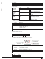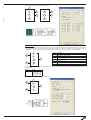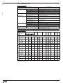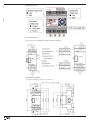
1
LRX D01
GB USER'S MANUAL OF PROGRAMMABLE LOGIC LRD RELAYS
I185 GB 06 10
LOVATO ELECTRIC S.P.A.
24020 GORLE (BERGAMO) ITALIA
VIA DON E. MAZZA, 12
TEL. 035 4282111
TELEFAX (Nazionale): 035 4282200
TELEFAX (International): +39 035 4282400
E-mail [email protected]
Web www.LovatoElectric.com
LRX D01
Contents
Summary of changes
4
Chapter 1: Getting Started
Precaution for Installation
Precaution for Wiring
Precaution for Operation
Examination before Installation
Environmental Precautions
Disclaim of Liability
LRD - Model Identification
5
5
5
5
5
5
5
6
Quick Start Setup
Install LRXSW Software
Connect Power to LRD relay
Connect Programming Cable LRXC00
Establish Communication
Write simple program
6
6
7
7
7
8
Chapter 2: Installation
General Specifications
Product Specifications
Mounting
WIRING
11
11
12
13
14
Chapter 3: Program Tools
PC Programming Software LRXSW
Installing the Software
Connecting the Software
Start Screen
Ladder Logic Programming Environment
Menus, Icons and Status Displays
Programming
Simulation Mode
Establish Communication
Writing Program to LRD relay
Operation menu
Online Monitoring/Editing
HMI/TEXT
Program Documentation
Symbol...
Line Comments
AQ Set…
Data Register Set…
Program Backup Memory (LRXM00)
LCD Display and Keypad
Keypad
Original Screen
LCD Display Main Menu
RTC Summer/Winter setting
16
16
16
16
17
17
18
18
19
20
20
21
22
22
25
25
25
26
26
27
28
28
28
29
33
Chapter 4: Relay Ladder Logic Programming
Common Memory Types
Specialty Memory Types
Output Instructions
Set Output Instruction (Latch)
Reset Output Instruction (Unlatch)
Pulse Output Instruction (Flip-Flop)
Analog memory type
Timer Instruction
Timer Mode 0 (Internal Coil)
Timer Mode 1 (ON-Delay)
Timer Mode 2 (ON-Delay with Reset)
Timer Mode 3 (OFF-Delay)
Timer Mode 4 (OFF-Delay)
Timer Mode 5 (FLASH without reset)
Timer Mode 6 (FLASH with Reset)
Timer Mode 7 (FLASH Cascade without Reset)
35
35
37
38
38
38
38
38
39
39
40
41
42
43
44
45
46
1
LRX D01
I185 GB 06 10
Counter Instructions
Common Counter
Counter Mode 0 (Internal coil)
Counter Mode 1 (Fixed Count, Non-Retentive)
Counter Mode 2 (Continuous Count, Non-Retentive)
Counter Mode 3 (Fixed Count, Retentive)
Counter Mode 4 (Continuous Count, Retentive)
Counter Mode 5 (Continuous Count, Up-Down Count, Non-Retentive)
Counter Mode 6 (Continuous Count, Up-Down Count, Retentive)
High Speed Counters (DC Version Only)
High Speed Counter Mode 7 (DC powered versions only)
High Speed Counter Mode 8 (DC powered versions only)
Real Time Clock (RTC) Instructions
RTC Mode 0 (Internal Coil)
RTC Mode 1 (Daily)
RTC Mode 2 (Interval weekly)
RTC Mode 3 (Year-Month-Day)
RTC Mode 4 (30-second adjustment)
Comparator Instructions
Comparator Mode 0 (Internal Coil)
Analog comparator Mode 1~7
HMI Display Instructions
HMI function instruction
PWM Output Instruction (DC Transistor Output Models Only)
PWM mode
PLSY mode
SHIFT (shift output)
AQ (Analog Output)
AQ display
AS (Add-Subtract)
MD (MUL-DIV)
PID (Proportion- Integral- Differential)
MX (Multiplexer)
AR (Analog-Ramp)
Timing diagram for AR
DR (Data register)
Chapter 5: Function Block Diagram Programming
FBD Instructions
Coil Block Instruction
HMI
PWM function block (only transistor output version)
PWM mode
PLSY mode
Data Link function block
SHIFT function block
Timing diagram
Logic Block Instructions
AND Logic Diagram
AND (EDGE) Logic Diagram
NAND Logic Diagram
NAND (EDGE) Logic Diagram
OR Logic Diagram
NOR Logic Diagram
XOR Logic Diagram
SR Logic Diagram
NOT Logic Diagram
Pulse Logic Diagram
BOOLEAN Logic Diagram
Function Block
Timer Function Block
Common Counter function block
High Speed Counter Function Block
RTC Comparator Function Block
Analog Comparator Function Block
AS (ADD-SUB) function block
MD (MUL-DIV) function block
PID (Proportion- Integral- Differential) function block
MX (Multiplexer) function block
AR (Analog-Ramp) function block
Chapter 6: Hardware Specification
Normal Specification
Product Specifications
Power Specifications
Normal model machine Specifications
Input Specifications
LRD...A240 MODEL
LRD...A024 MODEL
LRD12..D024 MODEL
LRD20..D024 MODEL
Output Specifications
Output Port wiring notice
Light Load
Inductance Load
Life of relay
Accessory
LRD dimensions
2
47
47
48
49
50
51
51
52
53
54
54
55
56
56
57
59
60
61
63
63
64
65
66
67
68
68
70
71
71
72
73
73
74
75
75
76
78
78
78
79
79
79
79
80
80
80
80
81
81
81
81
82
82
82
82
82
83
83
84
85
87
90
90
92
95
95
95
96
96
97
97
97
98
98
98
98
98
99
99
100
100
100
100
101
101
101
LRX D01
Chapter 7: Expansion Module
Digital IO module
Wiring
Communication module
ModBus LREP00 module
LREP00 ModBus Configuration
Connection with power source
Communication setting
State indication and trouble shooting
102
102
105
106
106
107
107
107
107
I185 GB 06 10
Appendix: Keypad Programming
Appendix A: Keypad programming in Ladder mode
Appendix B: Keypad programming in Ladder function block
108
108
113
3
LRX D01
SUMMARY OF CHANGES
This user manual is modified by firmware V3.0 and LRXSW programming software ver. 3. LRD V3.0 adds some new functions with firmware
version V3.0 to strong LRD function. The upgrade content is shown as the 2 tables below simply. More information about idiographic function to
see function instruction.
EDIT AND DISPLAY
I185 GB 06 10
LRD V3.0
LRD V2.x
Ladder
300 lines
200 lines
FBD
260 blocks
99 blocks
LCD
4 lines * 16 characters
4 lines * 12 characters
CONTACT AND FUNCTION BLOCK
input
output
Auxiliary relay M
M
M
63(M01~M3F)
15(M1~MF)
Auxiliary relay N
N
N
63(N01~N3F)
Ladder: NO
FBD: 15(N1~NF)
temperature input
AT
4(AT01~AT04)
No
AQ
4(AQ01~AQ04)
No
2(P01~P02, P01 adds PLSY mode)
1(P1: PWM)
analog output
PWM
P
HMI
LRD V2.x
31(H01~H1F)
15(H1~HF)
Timer
T
T
Ladder: 31(T01~T1F)
FBD: 250(T01~TFA)
15(T1~TF)
Counter
C
C
Ladder: 31(C01~C1F)
FBD: 250(C01~CFA)
15(C1~CF)
RTC
R
R
Ladder: 31(R01~R1F)
FBD: 250(R01~RFA)
15(R1~RF)
Analog Comparator
G
G
Ladder: 31(G01~G1F)
FBD: 250(G01~GFA)
15(G1~GF)
AS (Add-Sub)
No
No
Ladder: 31(AS01~AS1F)
FBD: 250(AS01~ASFA)
No
MD (Mul-Div)
Ladder: 31(MD01~MD1F)
FBD: 250(MD01~MDFA)
No
PID
Ladder: 15(PI01~PI0F)
FBD: 30(PI01~PI1E)
No
MX (Multiplexer)
Ladder: 15(MX01~MX0F)
FBD: 250(MX01~MXFA)
No
AR (Analog Ramp)
Ladder: 15(AR01~AR0F)
FBD: 30(AR01~AR1E)
No
DR (Data Register)
240(DR01~DRF0)
No
MU (MODBUS)
Ladder: 15(MU01~MU0F)
FBD: 250(MU01~MUFA)
No
Block
LRXM00 (version 3)
4
LRD V3.0
B
B
Logic function: BOOLEAN
No
260(B001~B260)The capability of
each block is alterable, and the total
capability of block is 6000bytes
99(B01~B99)The capability of each
block is fixed
LRXM00 (ver. 3) can be used with all
versions of LRD
LRXM00 cannot be used with LRD V3.x
LRX D01
CHAPTER 1: GETTING STARTED
The LRD Relay is an electronic device. For safety reasons, please carefully read and follow the paragraphs with "WARNING" or "CAUTION"
symbols. They are important safety precautions to be aware of while transporting, installing, operating, or examining the LRD Controller.
I185 GB 06 10
WARNING: Personal injury may result from improper operation.
CAUTION: The LRD relay may be damaged by improper operation.
PRECAUTION FOR INSTALLATION
Compliance with the installation instructions and the user manual is absolutely necessary. Failure to comply could lead to improper
operation, equipment damage or in extreme cases even death, serious bodily injury or considerable damage to property.
When installing the open-board models, insure that no wiring or foreign materials can fall into the exposed circuits and components.
Damage to equipment, fire, or considerable damage to property could result.
Always switch off power before you wire, connect, install, or remove any module.
The wiring for the LRD relay is open and exposed. For the open-board models, all electrical components are exposed. For this reason, it
is recommended the LRD relay be installed in an enclosure or cabinet to prevent accidental contact or exposure to the electrical circuits
and components.
Never install the product in an environment beyond the limits specified in this user manual such as high temperature, humidity, dust,
corrosive gas, vibration, etc.
PRECAUTION FOR WIRING
Improper wiring and installation could lead to death, serious bodily injury or considerable damage to property.
The LRD relay should only be installed and wired by properly experienced and certified personnel.
Make sure the wiring of the LRD relay meets all applicable regulations and codes including local and national standards and codes.
Be sure to properly size cables for the required current rating.
Always separate AC wiring, DC wiring with high-frequency switching cycles, and low-voltage signal wiring.
PRECAUTION FOR OPERATION
To insure safety with the application of the LRD relay, complete functional and safety testing must be conducted. Only run the LRD after
all testing and confirming safe and proper operation is complete. Any potential faults in the application should be included in
the testing. Failure to do so could lead to improper operation, equipment damage or in extreme cases even Death, serious bodily injury or
considerable damage to property.
When the power is on, never contact the terminals, exposed conductors or electrical components. Failure to comply could lead to
improper operation, equipment damage or in extreme cases even death, serious bodily injury or considerable damage to property.
It is strongly recommended to add safety protection such as an emergency stop and external interlock circuit in case the LRD relay
operation must be shut down immediately.
EXAMINATION BEFORE INSTALLATION
Every LRD relay has been fully tested and examined before shipment. Please carry out the following examination procedures after unpacking
your LRD relay.
– Check to see if the model number of the LRD matches the model number that you ordered.
– Check to see whether any damage occurred to the LRD during shipment. Do not connect the LRD relay to the power supply if there is any
sign of damage.
Contact Customer Service (Tel. +39 035 4282422 - E-mail: [email protected]) if you find any abnormal conditions as mentioned above.
ENVIRONMENTAL PRECAUTIONS
The installation site of the LRD relay is very important. It relates directly to the functionality and the life span of your LRD. Please carefully
choose an installation site that meets the following requirements:
– Mount the unit vertically
– Environment temperature: -20°C...55°C (-4°F...131°F)
– Avoid placing LRD close to any heating equipment
– Avoid dripping water, condensation, or humid environment
– Avoid direct sunlight
– Avoid oil, grease, and gas
– Avoid contact with corrosive gases and liquids
– Prevent foreign dust, flecks, or metal scraps from contacting the LRD relay
– Avoid electric-magnetic interference (soldering or power machinery)
– Avoid excessive vibration; if vibration cannot be avoided, an anti-rattle mounting device should be installed to reduce vibration.
DISCLAIM OF LIABILITY
We have reviewed the contents of this publication to ensure consistency with the hardware and software described. Since variance cannot be
precluded entirely, we cannot guarantee full consistency. However, the information in this publication is reviewed regularly and any necessary
corrections are included in subsequent editions.
5
LRX D01
LRD - MODEL IDENTIFICATION
a
b
c
d
I185 GB 06 10
a. LR ➞ Programmable relay series LR...
b. D
E
➞ Base model with display
➞ Expansion module
c. 10
12
20
08
P00
➞
➞
➞
➞
➞
Base module, 6 digital inputs + 4 digital outputs
Base module, 8 digital inputs ❶ + 4 digital outputs
Base module, 12 digital inputs ❷ + 8 digital outputs
Expansion module, 4 digital inputs + 4 digital outputs
MODBUS communication module
e
d. R
T
➞ Digital relay outputs
➞ Digital transistor outputs
e. A240 ➞ Supply voltage 100…240VAC
D024 ➞ Supply voltage 24VDC
A024 ➞ Supply voltage 24VAC
❶ The D024 version is equipped with 2 digital inputs that can be used as 0…10VDC analog type.
❷ The D024 version is equipped with 4 digital inputs that can be used as 0….10VDC analog type.
CODE COMPOSITION FOR LRD PROGRAMMABLE RELAY ACCESSORIES
a
b
a. LRX ➞ LRD programmable relay accessory
b. C00 ➞
D00 ➞
D01 ➞
D02 ➞
D03 ➞
M00 ➞
SW ➞
Connecting cable for PC ↔ LRD base module
User's manual Italian edition (paper)
User's manual English edition (paper)
User's manual Spanish edition (paper)
User's manual French edition (paper)
Program backup memory
Programming and supervision software (CD-ROM)
QUICK START SETUP
This section is a simple 5-steps guide to connecting, programming and operating your new LRD relay. This is not intended to be the complete
instructions for programming and installation of your system. Many steps refer to other sections in the manual for more detailed information.
INSTALL LRXSW SOFTWARE
Install the LRXSW Software from CD or from the free internet download at Customer Service (Tel. +39 035-4282422,
e-mail: [email protected])
6
LRX D01
CONNECT POWER TO LRD RELAY
Connect power to the LRD Relay using the below wiring diagrams for AC or DC supply for the applicable modules. See “Chapter 2: Installation”
for complete wiring and installation instructions.
24VDC
I185 GB 06 10
24VAC
100...240VAC
50/60Hz
VAC
VDC
CONNECT PROGRAMMING CABLE LRXC00
Remove the plastic connector cover from the LRD using a flathead screwdriver as shown in the figure below. Insert the plastic connector end of
the programming cable into the LRD relay as shown in the figure below. Connect the opposite end of the cable to an RS232 serial port on the
computer.
ESTABLISH COMMUNICATION
a. Open the LRXSW software and select “New Ladder Document” as shown below.
b. Select “Operation/Link Com Port…” as shown below.
7
LRX D01
I185 GB 06 10
c. Select the correct Com Port number where the programming cable is connected to the computer then press the “Link” button.
d. The LRXSW will then begin to detect the connected LRD relay to complete its connection.
WRITE SIMPLE PROGRAM
a. Write a simple one rung program by clicking on the leftmost cell at line 001 of the programming grid, then click on the “M” contact icon on
the ladder toolbar, as shown below. Select M01 and press the OK button. See Chapter 4: Ladder Programming instructions for complete
instruction set definitions.
Note: If the ladder toolbar is not visible at the bottom of the screen, select View>>Ladder Toolbar from the menu to enable.
8
LRX D01
I185 GB 06 10
b. Use the “A” key on your keyboard (or the “A” icon on the ladder toolbar) to draw the horizontal circuit line from the M contact to the right
most cell, as shown below.
c. Select the “Q” coil icon from the ladder toolbar and drop it on the right most cells. Select Q01 from the dialog and press OK as shown below.
See Chapter 4: Ladder Programming instructions for complete instruction set definitions.
d. Test the simple program. From the Operation menu, select the Write function and write the program to the connected LRD relay as shown
below.
9
LRX D01
I185 GB 06 10
e. Select the RUN icon from the toolbar, and select “No” when the pop-up message asks “Do you want to read program from module?”, as
shown below.
f. On the Input Status dialog, click on M01 to activate the contact M01 which will turn ON the Output Q01 as shown below. The highlighted
circuit will show active and the first Output (Q01) on the connected LRD relay will be ON. See Chapter 3: Programming Tools for more
detailed software information.
10
LRX D01
CHAPTER 2: INSTALLATION
GENERAL SPECIFICATIONS
LRD is a miniature Relay with a maximum of 44 I/O points and can be programmed in Relay Ladder Logic or FBD (Function Block Diagram)
program. The LRD can expand to its maximum I/O count by adding 3 groups of 4-input and 4-output modules.
I185 GB 06 10
POWER SUPPLY
Input Power Voltage Range
24V DC Models: 20.4-28.8V
12V DC Models: 10.4~14.4V
AC Models: 85-265V
24V AC Models: 20.4-28.8V
Power Consumption
24VDC: 12-point :125mA - 20-point: 185mA
12VDC: 12-point: 195mA - 20-point: 265mA
100-240VAC: 100mA
24VAC: 290mA
Wire Size (all terminals)
26 to 14 AWG
PROGRAMMING
Programming languages
Ladder/Function Block Diagram
Program Memory
300 Lines or 260 Function Blocks
Programming storage media
Flash
Execution Speed
10ms/cycle
LCD Display
4 lines x 16 characters
TIMERS
Maximum Number
Ladder: 31; FBD: 250
Timing ranges
0.01s-9999min
COUNTERS
Maximum Number
Ladder: 31; FBD: 250
Highest count
999999
Resolution
1
RTC (REAL TIME CLOCK)
Maximum Number
Ladder: 31; FBD: 250
Resolution
1min
Time span available
week, year, month, day, hour, minutes
Compare Instructions (Analog, Analog*gain + Offset, Timer, Counter, Temperature Input (AT), Analog Output (AQ), AS, MD, PI, MX, AR and
DR Values)
ANALOG COMPARE
Maximum Number
Ladder: 31; FBD: 250
Compare versus other inputs
Analog, Timer, Counter, Temperature Input (AT), Analog Output (AQ),
Analog*gain + Offset, AS, MD, PI, MX, AR , DR , or Numeric values
AMBIENT CONDITIONS
Enclosure Type
IP20
Maximum Vibration
1G according to IEC/EN 60068-2-6
Operating Temperature Range
-20°...55°C (-4°...131°F)
Storage Temperature Range
-40°...70°C (-40°...158°F)
Maximum Humidity
90% (Relative, non-condensing)
Vibration
0.075mm amplitude, 1.0g acceleration
Weight
8-point: 190g
10,12-point: 230g
20-point: 345g
Certifications
cULus, CE
DISCRETE INPUTS
Current consumption
3.2mA - 24VDC
4mA - 12VDC
1.3mA - 100-240VAC
3.3mA - 24VAC
Input Signal ”OFF” Threshold
24VDC: < 5VDC;
12VDC: < 2.5VDC
100-240VAC : < 40VAC
24VAC: <6VAC
Input Signal ”ON” Threshold
24VDC: > 15VDC;
12VDC: > 7.5VDC
100-240VAC : > 79VAC
24VAC: >14VAC
Input On delay
24, 12VDC: 5ms
240VAC: 25ms;
120VAC: 50ms
24VAC: 5ms
Input Off Delay
24, 12VDC: 3ms
240VAC: 90/85ms 50/60Hz ;
120VAC: 50/45ms 50/60Hz
24VAC: 3ms
Transistor device compatibility
NPN, 3-wire device only
High Speed Input frequency
1kHz
Standard Input frequency
< 40 Hz
Required protection
Inverse voltage protection required
11
LRX D01
I185 GB 06 10
ANALOG INPUTS
Resolution
Basic unit: 12 bit
Expansion unit: 12bit
Voltage Range acceptable
Basic unit: Analog input: 0-10VDC voltage,
24VDC when used as discrete input;
Expansion unit: Analog input: 0-10VDC voltage or 0-20mA current
Input Signal ”OFF” Threshold
< 5VDC (as 24VDC discreet input)
Input Signal ”ON” Threshold
> 9.8VDC (as 24VDC discreet input)
Isolation
None
Short circuit protection
Yes
Total number available
Basic unit: A01-A04
Expansion unit: A05-A08
RELAY OUTPUTS
Contact material
Ag Alloy
Current rating
8A
HP rating
1/3HP@120V 1/2HP@250V
Maximum Load
Resistive: 8A /point
Inductive: 4A /point
Maximum operating time
15ms (normal condition)
Life expectancy (rated load)
100k operations
Minimum load
16.7mA
TRANSISTOR OUTPUTS
PWM max. output frequency
1.0kHz (0.5ms on,0.5ms off)
Standard max. output frequency
100Hz
Voltage specification
10-28.8VDC
Current capacity
1A
Maximum Load
Resistive: 0.5A/point
Inductive: 0.3A/point
Minimum Load
0.2mA
PRODUCT SPECIFICATIONS
Moduli base
Order code
Input Power
Inputs
Outputs
Display & Keypad
Max I/O
LRD12RD024
24VDC
6 DC, 2 Analog
4 Relay
3, Z01-Z04
36 + 4 *1
LRD12TD024
24VDC
6 DC, 2 Analog
4 Transistor
3, Z01-Z04
36 + 4 *1
LRD20RD024
24VDC
8 DC, 4 Analog
8 Relay
3, Z01-Z04
44 + 4 *1
LRD20TD024
24VDC
8 DC, 4 Analog
8 Transistor
3, Z01-Z04
44 + 4 *1
LRD10RA240
100-240VAC
6 DC
4 Relay
3, Z01-Z04
34+ 4 *1
LRD20RA240
100-240VAC
12 DC
8 Relay
3, Z01-Z04
44 + 4 *1
LRD12RA024
24VAC
8 DC
4 Relay
3, Z01-Z04
36 + 4 *1
LRD20RA024
24VAC
12 DC
8 Relay
3, Z01-Z04
44 + 4 *1
Expansion Modules
LRE08RD024
24VDC
4 DC
4 Relay
N/A
N/A
LRE08TD024
24VDC
4 DC
4 Transistor
N/A
N/A
LRE08RA240
100-240VAC
4 DC
4 Relay
N/A
N/A
LRE08RA024
24VAC
4 DC
4 Relay
N/A
N/A
LREP00
24VDC
Communications Module, RS485 ModBus RTU slaver
Accessories
LRXC00
LRD Programming Cable, LRD Programming software
LRXM00
LRD program backup memory
*1 If module with keypad and display, Max IO can be added keypad input Z01-Z04.
2 More information about Product Specifications to see “chapter 6: Product Specifications”.
12
LRX D01
I185 GB 06 10
MOUNTING
35mm DIN-rail Mounting
The LRD relay must always be mounted vertically.
Place the upper end of the LRD relay inserting the slot on the DIN rail. Slightly press the relay downwards and fasten its lower end on the rail.
Check that the LRD is firmly fitted.
Insert the connector in the expansion module and fit the module on the DIN rail as previously described.
Slide the module on the rail toward the LRD relay, press the Press-button and connect them together.
Connector
+
-
DC 24V
I1 I2 I3
Input X1 X2 X3 X4
4¡ ÀC
I4 I5 I6 A1 A2
L
Input 8 x DC(A1,A2 0~10V)
Press-button
N AC 100~240V
Run
Output 4 x Relay / 8A
LRX M00
Output 4 x Relay / 8A
Y1
Y2
DIN Rail
Q1
Q2
Q3
Y3
Q4
Y4
It is recommended to apply a DIN-rail end clamp to hold the LRD in place.
+
-
DC 24V
I1 I2 I3 I4 I5 I6 A1 A2
Input 8 x DC(A1,A2 0~10V)
Input X1 X2 X3 X4
4¡ ÀC
N
L
End clamp
AC 100~240V
Run
Output 4 x Relay / 8A
LRX M00
Output 4 x Relay / 8A
Q1
Q2
Q3
Q4
Y1
Y3
Y2
DIN Rail
Y4
13
LRX D01
Screw Fixing
Use M4x20 screws to directly mount the LRD as shown. For direct installation of the expansion module, slide the expansion module and connect
with the Master after the Master is fixed.
I185 GB 06 10
M4x20 (#8x32)
+
-
DC 24V
I1 I2 I3 I4 I5 I6 A1 A2
Input X1 X2 X3 X4
4¡ ÀC
L
Input 8 x DC(A1,A2 0~10V)
M4x20 (#8x32)
N AC 100~240V
Run
Output 4 x Relay / 8A
LRX M00
Output 4 x Relay / 8A
Q1
Q2
Q3
Y1
Q4
Y2
Y3
Y4
WIRING
WARNING: The I/O signal cables must be routed parallel to the power cable, or in the same cable trays to avoid the signal interference.
To avoid a short circuit on the load side, it is recommended to connect a fuse between each output terminals and loads.
WIRE SIZE AND TERMINAL TORQUE
mm2
0.14...1.5
0.14...0.75
0.14...2.5
0.14...2.5
0.14...1.5
AWG
26...16
26...18
26...14
26...14
26...16
C
Ø3.5
(0.14in)
C
Nm
0.6
lbin
5.4
Input 24VDC
+-
A1 A2
1
1
24VDC
A1
A2
A3
A4
2
2
-
+
DC
14
+-
V
I1
I2
I3
Input
I4
I5
I6
A1
A2
+ -
DC
I1
V
I2
I3
I4
INPU T
I5
I6
I7
I8
A1 A2 A3 A4
LRX D01
Sensor Connection
I185 GB 06 10
24VDC
Input 100~240VAC/24VAC
1
24VAC
100...240VAC
50/60Hz
1
3
3
-
+
AC
V
I3
I4
I5
I6
A1
+ -
A2
AC
Input
I1
I2
I3
V
I4
I5
I6
I7
I8
A1 A2 A3 A4
INPU T
Output (Relay)
Output 4 x Relay / 8A
Q1
Q2
Output 8 x Relay / 8A
Q3
Q4
Q1
Q2
Q3
Q4
5
4
Q5
Q6
Q7
Q8
5
12...240VAC
50/60Hz
or 12...125VDC
12...125VDC
12...240VAC 50/60Hz
Output (Transistor)
OUTPUT 8 x TR / 0.5A
OUTPUT 4 x TR / 0.5A
+Q1 -
+Q2 -
+Q3 -
+Q4 -
+Q1 -
+Q2 -
+Q3 -
+Q4 -
+Q5 -
+Q6 -
+Q7 -
+Q8 -
5
4
24VDC
or
24VDC
12VDC
1 - 1A quick fuse, disconnect switch and circuit protections
2 - Transitory over-current surge suppressor (36VDC cut-off voltage)
3 - Transitory over-current surge suppressor (400VAC cut-off voltage)
4 - Fuse, disconnect switch and circuit protections
5 - Inductive load.
15
LRX D01
CHAPTER 3: PROGRAM TOOLS
I185 GB 06 10
PC PROGRAMMING SOFTWARE “LRXSW”
The LRD Client programming software provides two edit modes, Ladder Logic and Function Block Diagram (FBD). The LRD Client software
includes the following features:
1. Easy and convenient program creation and editing.
2. Programs can be saved on a computer for archiving and reuse. Programs can also be uploaded directly from a LRD and saved or edited.
3. Enables users to print programs for reference and review.
4. The Simulation Mode allows users to run and test their program before it is loaded to the controller.
5. Real-time communication allows the user to monitor and force I/O on the LRD relay operation during RUN mode.
INSTALLING THE SOFTWARE
Install the LRD Client Software from CD or from the free internet download contact Customer Service (Tel. +39 035 4282422 email: [email protected] ).
CONNECTING THE SOFTWARE
Remove the plastic connector cover from LRD using a flathead screwdriver as shown in the figure below.
Insert the plastic connector end of the programming cable into the LRD relay as shown in the figure below.
Connect the opposite end of the cable to an RS232 serial port on the computer. In case the computer does not have one, connect the LRX C00
cable to a RS232-USB converter, compatible with USB2.0 or higher.
16
LRX D01
I185 GB 06 10
START SCREEN
Run the LRXSW software and the below Start screen will be displayed. From this screen, you can perform the following functions
NEW LADDER PROGRAM
Select File —>New —>New LAD to enter the development environment for a new Ladder program.
NEW FBD PROGRAM
Select File —>New —>New FDB to enter the development environment for a new FBD (Function Block Diagram) program.
OPEN EXISTING FILE
Select File —>Open to choose the type of file to open (Ladder or FBD), and choose the desired program file, and then click Open.
LADDER LOGIC PROGRAMMING ENVIRONMENT
The Ladder Logic Programming Environment includes all the functions for programming and testing the LRD using the Ladder Logic
programming language. To begin a new program select File —>New, and select the desired model of LRD, and the number of connected
expansion units if applicable, as shown below.
17
LRX D01
I185 GB 06 10
MENUS, ICONS AND STATUS DISPLAYS
The Ladder programming environment includes the following Menus, Icons and Status Displays
1. MENU BAR - Five menu selections for program development and retrieval, editing, communication to connected controllers, configuration of
special functions and viewing preference selections.
2. MAIN TOOLBAR - (From Left to Right)
Icons for create a new program, open a program, save a program and print a program.
Icons for Keypad, Ladder view, HMI/Text edit and Symbol (comments) edit.
Icons for Monitor, Simulator, Simulator Controller, Controller Mode changes (Run, Stop, and Quit), and Read/Write programs from/to the
LRD relay.
3. Usage List - List for all memory types and addresses used with the current open program. Used addresses are designated by a “*” symbol
below each address.
4. Amount of free programming memory available.
5. Current Mode - operation mode of the controller, or simulator, from the connected PC.
6. Ladder Toolbar - Icons for selecting and entering all available Ladder Logic instructions.
7. Status Bar - Status of current open project and connect LRD relay.
PROGRAMMING
The LRXSW software can be programmed by either position of instructions or by using keyboard entry commands. Below is an example of
some common methods of entering programming instructions.
18
LRX D01
I185 GB 06 10
The “A” and “L” keys or icons are used to complete parallel and serial circuits. The right column is for output coils.
SIMULATION MODE
The LRXSW software includes a built-in simulator to test and debug programs easily without the need for downloading to a controller. To
activate simulation mode, simply press the red RUN icon. The program below is shown in simulation mode, identifying the significant available
features.
19
LRX D01
I185 GB 06 10
ESTABLISH COMMUNICATION
The following is the simple procedure for establishing communication between PC and the LRD relay.
a. Select “Operation/Link Com Port…” as shown below.
b. Select the correct Com Port number where the programming cable is connected to the computer then press the “Link” button.
c. The LRXSW software will then begin to detect the connected LRD relay to complete its connection.
WRITING PROGRAM TO LRD RELAY
From the Operation menu, select the Write function and write the program to the connected LRD relay as shown below, or press Write button to
write program to connected LRD relay as shown below.
20
LRX D01
I185 GB 06 10
OPERATION MENU
The Operation menu, includes several system configuration functions for both online and offline setup. The following explains the details of each
function.
Monitor - Online function for runtime monitor and editing when connected to a controller
Simulator - Offline function for testing and debugging a program.
Simulator Control - Self-motion simulator control
Run-Stop-Quit - Mode change selections for both runtime editing and simulation mode.
Read-Write - Reading and writing programs to and from a connected LRD relay.
RTC Set - Online function for setup of the Real-time clock/calendar (see dialog below left)
Analog Set - setup analog input A01-A08 gain and offset (see dialog below right)
Password - Set a password for accessing the current program after upload to the LRD relay
Language - Change LRD relay menu language
Module System Set - Dialog for changing important system setup functions including Module ID, Remote I/O preferences, Expansion I/O
settings, and Retentive memory preferences (Keeping) for (C) Counters, (M) Auxiliary Coils, and (Z) keypad input set and the LCD Backlight.
Link Com Port - Select the port communication with LRD relay.
21
LRX D01
I185 GB 06 10
ONLINE MONITORING/EDITING
The LRXSW software allows for online monitoring of the currently running program during runtime. Additional online functions include, I/O
forcing, and Mode changes (Run/Stop/Quit).
– The LRXSW software does not support runtime logic editing changes. All logic edits to contacts, coils, Timers/Counters, and circuit
connecting lines must be written to the connected LRD relay while in Stop mode.
HMI/TEXT
This function block can display information on 16_4 LCD screen. Information displaying can be present value or target value of Counter, Timer,
RTC and Analog comparator etc. Under running mode, to modify the target value of timer, counter and analog comparator via HMI is available.
HMI can display the status of input terminal (I, Z, X) and Auxiliary terminal M, N (only FBD).
22
LRX D01
I185 GB 06 10
HMI/TEXT setting:
1. Enter H01 coil.
2. Into HMI/TEXT edit frame.
3.-4. Choose the letters “T E S T” from Text Input.
5. Choose T01 current.
6. Choose T01 current (unit).
7. Choose T01 present (unit).
The user can modify T01 preset value when H coil enable and display on LCD.
Download to LRD, and I01 turn ON, or press “SEL” if the H coil is set to mode 1, then the LRD LCD will display the first H text as shown below.
– Press “” or “” to select the nearest H coil
– Press “SEL”+”” or “”and “OK” update T01 preset value (In this example, 050.0 can update, T01 preset value depends on HMI/TEXT edit
frame setting.)
23
LRX D01
I185 GB 06 10
HMI/TEXT Example:
Power ON and RUN (initial display)
Press “” (Z01) and display H03 coil
–
–
–
–
–
24
Press “SEL” to display cursor.
Press “”, “”, “”, “” to move cursor.
Press “SEL” again to select modified position.
Press ““”, “” to change number and press “”, “” to move cursor.
Press “OK” to make sure the modify value is confirmed.
LRX D01
I185 GB 06 10
Press “” to disable H03 coil, and the LCD display changes to initial frame.
Press “” to reset Timer (T01°¢T02°¢T03) as program designed.
PROGRAM DOCUMENTATION
The LRD Client software includes the ability to document a program using Symbols and Line Comments. Symbols are used to label each I/O
address up to a length of 12 characters. Line Comments are used to document sections of a program. Each Line Comment can have up to 4
lines with each line containing up to 50 characters in length. Below are examples of entering Symbols and Line Comments.
SYMBOL...
The Symbol editing environment can be access through the menu using the Edit>>symbol… selection or using the symbol icon on the main
toolbar shown below.
The Symbol editing environment allows for documenting all the contact and coil memory types, and selecting display modes as shown below.
LINE COMMENTS
The Line Comment editor is accessed by clicking the “N” icon on the Ladder Toolbar. After clicking on the “N” icon, to drag the line
number you want to comment and release, and then type the desired comments and press OK.
25
LRX D01
I185 GB 06 10
AQ SET…
The AQ editing environment can be access through the menu using the Edit>> AQ Set… selection shown below. The range of AQ is 0~1000 if
the output mode of AQ is voltage mode. And the range is 0~500 if the output mode is current mode. The preset value of AQ can be set as either
a constant or a code of other data. The output mode of AQ and preset value are set as below. More information about output mode and
displaying to see: Chapter 4: Relay Ladder Logic Programming
DATA REGISTER SET…
The content of Data Register is either unsigned or sign, it can be set as shown below. Selecting Unsigned, the range of DR is 0~65535; and
selecting Signed, the range of DR is -32768~32767.
After the operating above, the Data Register editing environment can be access through the menu using the Edit>> Data Register Set…
selection shown below. The preset value of DR can be set as either a constant or a code of other data type.
26
LRX D01
I185 GB 06 10
DR is set as signed shown below.
PROGRAM BACKUP MEMORY (LRXM00)
LRMX00 can be used with all LRD versions. There is an icon 3rd on LRD relay, V3.0, and on LRMX00 memory, version 3.
About to use PM05 and PM05 (3rd) with LRDV2/3, see next figure:
The optional LRXM00 memory is used to easily transfer programs from one LRD relay to another.
LRD
Vers. 2
LRXM00
Vers. 3 or inferior
LRD
Vers. 2 and 3
LRD
Vers. 3
LRXM00
Vers. 3
LRD
Vers. 3
The LRXM00 memory plugs into the same connector as the programming cable (see procedure below).
1. Remove the plastic connector cover from LRD using a flathead screwdriver as shown in the figure below left.
2. Insert the LRXM00 memory onto the connector as shown below right.
3. From the display keypad on the face of the LRD relay, select either WRITE or READ to transfer the program to LRXM00 or from the LRXM00
memory to the LRD relay.
4. Program in different types are not compatible, here are the regulations:
A-1: 10/12 point type program —— available in 20 point type
A-2: 20 point type program —— unavailable in 10/12 point type
B-1: AC type program —— available in DC type
B-2: DC type program —— unavailable in AC type
C-1: Relay type program —— available in Transistor type
C-2: Transistor type program —— unavailable in Relay type
D-1: LRD V2.0 program —— available LRD V3.0 type
D-2: LRD V3.0 program —— unavailable LRD V2.0 type
27
LRX D01
LCD DISPLAY AND KEYPAD
I185 GB 06 10
KEYPAD
Most LRD CPU units include the built-in LCD Display and Keypad. The keypad and display are most often used for changing timer/counter set
points, controller mode changes (Run/Stop), uploading/downloading to the PM05 memory cartridge, and updating the RTC (Real Time
Clock/Calendar). Although, logic programming can be performed from the keypad and display, it is highly recommended to only perform logic
changes using the LRDSW software. Below is an overview of the basic keypad and display functions.
Select (SEL) - Used to select the available memory and instruction types for editing. Holding the Select button will display all “H” HMI/Text
messages on the LCD.
OK - Used to accept the selection displayed of an instruction or function. It is also used to select any of the Main Menu options on the LCD.
Note: Press the “SEL” and “OK” simultaneously to insert a rung above the current active cursor position.
Escape - Used to exit a selected display screen and go to the previous screen. When in a ladder display screen, press the ESC to display the
main menu.
Delete - Used to delete an instruction or rung from the ladder program.
The 4 navigation buttons () are used to move the cursor throughout the functions of the LRD display or active program. The 4 buttons
also can be set programmable input coils Z01-Z04 (‘’= Z01, ‘’=Z02, ‘’=Z03, ‘’ =Z04).
ORIGINAL SCREEN
LCD displays 4-line state
– Original screen as power on
Press the button:
ESC
SEL + /
/
SEL
SEL+OK
– Expansion display State
28
Enter Main Menu screen
Under LADDER Mode, display the state of relays (I Z Q X Y M N T C R G A AT AQ) Original Screen
Under FBD Mode, display the state of relays (I Z Q X Y M N A AT AQ) Original Screen
H Function will be displayed whose mode is 1 as the button is pressed.
Enter RTC setting screen
– Other Display State
Ladder edit mode: Coil I, Z, X, Q, Y, M, N, T, C, R, G, D, Analog input A01~A04, Expansion Analog input A05~A08, temperature analog input
AT01~AT04, analog output AQ01~AQ04;
FBD edit mode: Coil I, Z, X, Q, Y, M, N, Analog input A01~A04, Expansion Analog input A05~A08, temperature analog input AT01~AT04, analog
output AQ01~AQ04;
I185 GB 06 10
LRX D01
– Expansion module setting: refer to Main Menu “SET”
LCD DISPLAY MAIN MENU
( 1 ) The Main Menu as LRD under 'STOP' Mode. Into ladder main function to press ESC after power on when the user program is ladder type
or empty program. Into FBD main function to press ESC after power on when the user program is FBD type or empty program.
>
>
>
>
LADDER
FUN. BLOCK
PARAMETER
RUN
DATA REGISTER
CLEAR PROG.
WRITE
READ
SET
RTC SET
ANALOG SET
PASSWORD
ANALOG SET
PASSWORD
LANGUAGE
INITIAL
>
>
>
>
FBD
PARAMETER
RUN
DATA REGISTER
Menu
Description
>
LADDER
Ladder edit
FUN.BLOCK
Ladder function block
(timer/counter/RTC …) edit
CLEAR PROG.
WRITE
READ
SET
RTC SET
ANALOG SET
PASSWORD
LANGUAGE
ANALOG SET
PASSWORD
LANGUAGE
INITIAL
FBD
FBD display
PARAMETER
FBD block or LADDER function
block parameter display
RUN
RUN or STOP
DATA REGISTER
DR display
CLEAR PROG.
Clear the user program and the password
WRITE
Save user program to LRXM00 (ver. 3)
READ
Read user Program from LRXM00 (ver. 3)
SET
System setting
RTC SET
RTC setting
ANALOG SET
Analog setting
PASSWORD
Password setting
LANGUAGE
Select the language
INITIAL
initially set Edit method
(2) The Main Menu as LRD under 'RUN' Mode.
>
LADDER
FUN. BLOCK
PARAMETER
STOP
>
FBD
PARAMETER
STOP
DATA REGISTER
>
LADDER
FUN.BLOCK
FBD
PARAMETER
STOP
DATA REGISTER
>
DATA REGISTER
WRITE
RTC SET
PASSWORD
>
WRITE
RTC SET
PASSWORD
LANGUAGE
>
WRITE
RTC SET
PASSWORD
LANGUAGE
WRITE
RTC SET
PASSWORD
LANGUAGE
29
LRX D01
Press the button
Move the Cursor to select Main Menu
OK
Confirm the selected Function
ESC
Skip to Initial Screen
– LRD can be modified, edited, cleared and read user program only when it is under STOP Mode.
– As the program is modified, LRD will automatically backup it to FLASH.
I185 GB 06 10
– Main Menu LADDER
Press the button
Button
SEL
SEL, then /
SEL, then /
//
Description
1. Ixx ixx — space Ixx (only for digital and character position of 1, 3, 5 column.)
2. Qxx space Qxx (only for digital and character position of 8 column.).
3.
space (all available but the 2,4,6 column of the first line)
1. I X Z Q Y M N D T C R G I (When the cursor located at 1, 3, 5 Column).
2. Q Y M N T C R G H L P S AS MD PI MX AR DR MU Q (When the cursor located at 8 Column)
3. ( P (When the cursor located at 7 Column, and the 8 Column is set as Q, Y, M, N)
4. ( P (When the cursor located at 7 Column, and the 8 Column is set as T)
Confirm the input data and move the cursor
move the cursor
DEL
Delete an instruction
ESC
1. Cancel the Instruction or action under Edition.
2. Back to Main Menu after query the program (save program).
OK
1. Confirm the data and automatically save, the cursor moves to next input position.
2. When the cursor is on Column 8, Press the button to automatically enter the function block and set the
parameters (such as T/C)
SEL + DEL
Delete a Line of Instruction.
SEL + ESC
Display the number of the Lines and operation state of LRD (RUN/STOP)
SEL + /
SEL + OK
Skip up/ down every 4-line program.
Insert a space line
Operation Sample: more detailed to see appendix A.
– FUNCTION BLOCK program input
Into FUNCTION BLOCK, cursor flicker on “T”, press “SEL” key, Ladder function block display in sequence:
TCRGHLPSASMDPIMXARMUT...
Operation Sample: more detailed to see Appendix B.
30
LRX D01
I185 GB 06 10
– PARAMETER
Under Ladder mode, press “SEL” key, function block display in sequence:
TCRGASMDPIMXARMUT...
Under FBD mode, Press “SEL” key, Block displays in sequence.
– RUN or STOP
(1) RUN Mode
/
(2) STOP Mode
Move the cursor
OK
Execute the instruction, then back to main menu
ESC
Back to main menu
– DATA REGISTER
Displaying preset value when the LRD is STOP status and displaying current value when the LRD is RUN status.
DR01 = 0000
DR02 = 0000
DR03 = 0000
DR04 = 0000
SEL + DR05 = 0000
DR06 = 0000
DR07 = 0000
DR08 = 0000
Move the cursor
OK
Ensure the edit
SEL
Enter edit (edit DR display number or DR preset value)
‘SEL’ then ‘SEL’
Edit DR preset value type
‘SEL’ then ‘/‘
1. Edit DR display number (only first line)
2. Edit DR preset value
ESC
SEL + /
1. Cancel edit.
2. Back to main menu (save DR preset data)
Tip-up/down page
– Other Menu Items
(1) CLEAR PROGRAM (Clear RAM, EEPROM and Password at the same time)
(2) WRITE: save the program (RAM) to PM05 (3rd) program spare cartridge
(3) READ: read the program from the PM05 or PM05 (3rd) program spare cartridge to LRD (RAM)
31
LRX D01
(1) - (3) Now press
/
Move the cursor
OK
Execute the instruction
ESC
Back to main menu
(4) SET (system setting)
I185 GB 06 10
ID SET
REMOTE I/O
BACKLIGHT
M KEEP
01
N
X
✔
I)O NUMBER:
I/O ALARM
C KEEP
Z SET
0
✔
X
X
V COMM SET
DATA REG.
03
U
content
default
ID SET
01
ID setting (00~99)
REMOTE I/O
N
Remote I/O Mode
(N: none M: Master S: Slave)
BACK LIGHT
X
Back light mode
(3: always light x: light for 10s after pressed.)
M KEEP
3
M: non-Volatile (3:Volatile x: Non- Volatile)
I/O NUMBER
0
Setting expansion I/O module number (0~3)
I/O ALARM
3
Siren setting when is not available to Expansion I/O Points
(3:Yes _:No)
C KEEP
X
In stop/run switching, Counter Present Value Keeping
(3:Yes x:No)
Z SET
X
Enable or disable keypad input Z01-Z04
(3:enable x:disable)
V COMM SET
03
Setting the form and baud rate of RS-485
DATA REG.
U
Setting the Data Register type
(U: 16bit-unsiged S: 16bit-sign)
– M KEEP function is available for keeping M status and current value of T0E/T0F when power is re-supplied after loss.
Now press
SEL
‘
Move the cursor
Begin to edit.
SEL’ quindi ‘/‘
Move the cursor for 'ID SET' item and 'V COMM SET' item
‘SEL’ quindi ‘/‘
1. ID SET = 00~99 ; I/O NUMBER = 0~3
2. REMOTE I/O = NMSN
3. BACK LIGHT ; C KEEP ; Z SET = x3
4. M KEEP; I/O ALARM = 3x
5. V COMM SET = (0~3)(0~5)
6. DATA REG. = US
OK
Confirm the Edition Data
ESC
1. Cancel the setting when pressed 'SEL'
2. Back to Main Menu(save edit data)
– When DATALINK is selected, ID setting range is 0~7, which should be continuous.
ID=0 default as Master, ID=1~7 default as Slave.
– When REMOTE I/O is selected, the distribution of the remote I/O is as follows:
Master
Slave
Remote Input
X01~X0C
I01~I0C
Remote Output
Y01~Y08
Q01~Q08
– The high bit of V COMM SET detects the form of RS-485, and the low bit detects the baud rate of RS-485.
More detailed to see chapter 4: Relay Logic Programming: Data Link/Remote IO Instruction
(5) RTC SET
Now press
Enter RTC setting or Summer/Winter setting
SEL
Begin to input parameters
‘SEL’ then ‘/‘
Move the Cursor
‘SEL’ then ‘/‘
1. year=00~99, month=01~12, day=01~31
2. week: MOTUWETHFRSASU‘MO
3. hour = 00~23 , minutes = 00~59
‘SEL’ then ‘SEL’
Summer/Winter setting: NO - EUROPE - USA - OTHER - NO …
OK
Save the Input Data
ESC
1. Cancel the Input Data when press 'SEL'.
2. Back to Main Menu.
– RTC precision
32
Temperature
Error
+25°
±3 s/day
-20°C/+50°C
±6 s/day
LRX D01
RTC SUMMER/WINTER SETTING
There are 2 fixed Summer/Winter, EUROPE and USA, 1 edit Summer/Winter in LRD.
Edit rule:
1. The last Sunday is defined as 0;
2. Hour range: 1~22;
3. Summer hour and Winter hour are the same.
Summer/Winter can be set through the two methods as shown below.
I185 GB 06 10
1) PC Client
2) Keypad
Then pressing “” selects edit location, pressing “”, “” edit content.
Example:
Year 2009, SUM M: 05 D: 01 32009-5-3; M: 10 D: 00 2009-10-25.
6. ANALOG SET
A 1=GAIN : 010
GAIN (0~999), default 10
OFFSET : +00
OFFSET (-50~+50), default 0
A 2=GAIN : 010
OFFSET : +00
A3~A8...Gain + Offset
Now press
1. Move the Cursor downward
2. Switch the setting screen from A01/A02í A03/A04í A50/A06 í A07/A08
SEL
Begin to input parameters
‘SEL’ then ‘/‘
Move the Cursor
‘SEL’ then ‘/‘
1. GAIN =000 ~ 999
2. OFFSET=(-50 ~ +50)
OK
Save the Input Data
ESC
1. Cancel the Input Data when press 'SEL'.
2. Back to Main Menu (save edit data).
– V01 = A01*A01_GAIN + A01_OFFSET …… V08 = A08*A08_GAIN + A08_OFFSET
33
LRX D01
7. PASSWORD (setting password)
I185 GB 06 10
Now press
SEL
1. Begin to input numeral
2. When the password is ON, it will not display 0000, but ****.
‘SEL’ then ‘/‘
Move the cursor
‘SEL’ then ‘/‘
Data changed 0~F
OK
Save the input data, not 0000 or FFFF, as the PASSWORD is ON.
ESC
1. Cancel the Input Data when press 'SEL'.
2. Back to Main Menu.
– A Class: Password number is set to 0001~9FFF.
B Class: Password number is set to A000~FFFE.
Password number = 0000 or FFFF is disabled Password function, Default setting: 0000.
A/B Class password Description (3£0cannot use under password protected )
Menu
A Class
B Class
LADDER
3
3
FUN.BLOCK
3
3
FBD
3
3
PARAMETER
3
RUN/STOP
3
3
DATA REGISTER
CLEAR PROG.
3
3
WRITE
3
3
READ
3
3
3
SET
RTC SET
3
ANALOG SET
3
LANGUAGE
3
INITIAL
3
8. LANGUAGE (Selection menu language)
>
ENGLISH
FRANÇAIS
ESPAÑOL
ITALIANO
3
ITALIANO
DEUTSCH
PORTOGUES
>
English
French
Spanish
Italian
German
Portuguese
Simplified Chinese
Now press
Vertically move the Cursor
OK
Select the language the cursor located
ESC
Back to Main Menu
9. INITIAL (select Ladder Logic and Function Block Diagram (FBD))
INITIAL
>
LADDER
FBD
3
Now press
Vertically move the Cursor
OK
Select the mode the cursor located
ESC
Back to Main Menu
The origin program will be cleared as the change of edition method.
34
COMMON MEMORY TYPES
I185 GB 06 10
Symbol
[
SET
output
RESET
output
PULSE
output
➣
General
output
➣
LRX D01
CHAPTER 4: RELAY LADDER LOGIC PROGRAMMING
P
NO
contact
NC
contact
Number
(NO/NC)
Input contact
I
i
Keypad input
Z
z
12 (I01-I0C / i01-i0C)
4 (Z01-Z04 / z01-z04)
8 (Q01-Q08 / q01-q08)
Output coil
Q
Q
Q
Q
Q
q
Auxiliary relay
M
M
M
M
M
m
63 (M01-M3F / m01-m3F)
Auxiliary relay
N
N
N
N
N
n
63 (N01-N3F / n01-n3F)
Counter
C
C
c
31 (C01-C1F / c01-c1F)
Timer
T
T
t
31 (T01-T1F / t01-t1F)
T
INPUTS (I MEMORY TYPE)
The LRD digital input points are designated I memory types. The number of digital I input points is 6, 8 or 12 depending on each LRD model.
KEYPAD INPUTS (Z MEMORY TYPE)
The LRD keypad input points are designated Z memory types. The number of digital Z input points is 4.
OUTPUTS (Q MEMORY TYPE)
The LRD digital output points are designated Q memory types. The number of digital Q output points is 4 or 8 depending on each LRD model. In
this example, output point Q01 will be turned on when input point I01 is activated.
AUXILIARY RELAYS (M MEMORY TYPE)
Auxiliary relays ate digital internal memory bits used to control a ladder logic program. The auxiliary relays are not physical inputs or outputs
that can be wired to any external device, switches, sensors, relays, lamps, etc. The number of Auxiliary Relays M is 63. Since auxiliary relays are
internal bits within the CPU, they can be programmed as digital inputs (contacts) or digital outputs (coils). In the first rung of this example,
auxiliary relay M01 is being used as an output coil and will energize when input I02 turns on. In the second rung auxiliary relay M01 is being
used as an input and when energized, will turn on outputs Q02 and Q03.
35
LRX D01
I185 GB 06 10
– The state of auxiliary relays “M01~M3F” will be kept when the LRD powers down if “M Keep” is active. “M Keep” can be set by the two ways
below.
SPECIAL AUXILIARY RELAYS: M31~M3F
Code
Signification
Description
M31
User program upstart flag
Outputting ON during the first scanning period; and used as normal auxiliary
relay at other scan period.
M32
1s blinking output
0,5 s ON, 0,5 s OFF
M33
Summer/Winter output
Summer time turn ON, winter time turn OFF, used as normal auxiliary relay.
M34
Reserved
M35
Reserved
M36
Reserved
M37
Reserved
M38~M3C
Reserved
M3D
Received
M3E
Error flag
M3F
Time out
MODBUS function using
AUXILIARY RELAYS (N MEMORY TYPE)
Auxiliary relays N is the same to auxiliary relays M, but it cannot be kept when the LRD powers down.
In the first rung of this example, auxiliary relay N01 is being used as an output coil and will energize when input I03 turns on. In the second
rung auxiliary relay N01 is being used as an input and when energized, will turn on outputs Q04 and Q05.
TIMERS AND TIMER STATUS BITS (T MEMORY TYPE)
Timer status bits provide the relationship between the current value and the preset value of a selected timer. The timer status bit will be on when
the current value is equal or greater than the preset value of a selected timer. In this example, when input I03 turns on, timer T01 will start.
When the timer reaches the preset of 5 seconds timer status contact T01 turns on. When T01 turns on, output Q04 will turn on. Turning off I03
will reset the Timer.
36
LRX D01
I185 GB 06 10
COUNTERS AND COUNTER STATUS BITS (C MEMORY TYPE)
Counter status bits provide the relationship between the current value and the preset value of a selected counter. The counter status bit will be
on when the current value is equal or greater than the preset value of a selected counter. In this example, each time the input contact I04
transitions from off to on, the counter (C01) increments by one. When the counter reaches the preset of 2 counts, the counter status contact
C01 turns on. When C01 turns on, output Q05 will turn on. When M02 turns on counter C01 will reset. If M09 is turned on, the counter will
change from a count-up to a count-down counter.
Symbol
[
SET
output
RESET
output
PULSE
output
➣
General
output
➣
SPECIALTY MEMORY TYPES
P
Expansion input coil
Expansion output coil
Y
Differential (one shot)
Y
Y
Y
NO
contact
NC
contact
Lo
Hi
Number
(NO/NC)
Used in function
block
X
x
12 (X01-X0C / x01-x0C)
Y
y
12 (Y01-Y0C / y01-y0C)
D
d
RTC
R
R
r
Analog comparator
G
G
g
31 (R01-R1F / r01-r1F)
HMI
H
31 (H01-H1F)
PWM
P
2 (P01-P02)
DATA LINK
L
8 (L01-L08)
SHIFT
S
1 (S01)
31 (G01-G1F / g01-g1F)
POSITIVE INPUT DIFFERENTIAL INSTRUCTION (ONE-SHOT)
A positive input differential instruction, or One-Shot, holds its status ON for one CPU scan when the preceding series contact transitions from
OFF to ON. This transition from OFF to ON is called a Positive Input Differential.
NEGATIVE INPUT DIFFERENTIAL INSTRUCTION (ONE-SHOT)
A negative input differential instruction, or One-Shot, holds its status ON for one CPU scan when the preceding series contact transitions from
ON to OFF. This transition from ON to OFF is called a Negative Input Differential.
37
LRX D01
➣
OUTPUT INSTRUCTIONS
I185 GB 06 10
SET OUTPUT INSTRUCTION (LATCH) ( )
A set output instruction, or Latch, turns ON an output coil (Q) or an auxiliary contact (M) when the preceding input contact transitions from OFF
to ON. Once the output is ON or set, it will remain ON until it is reset using the Reset output instruction. It is not necessary for the preceding
input contact controlling the Set output instruction to remain ON.
➣
RESET OUTPUT INSTRUCTION (UNLATCH) ( )
A reset output instruction, or Unlatch, turns OFF a previous set output coil (Q) or an auxiliary contact (M) when the preceding input contact
transitions from OFF to ON. Once the output is OFF or reset, it will remain OFF until it if reset using another output instruction. It is not
necessary for the preceding input contact controlling the Reset output instruction to remain ON.
PULSE OUTPUT INSTRUCTION (FLIP-FLOP) (P)
A pulse output instruction, or Flip-Flop, turns ON a coil (Q) or an auxiliary contact (M) when the preceding input contact transition from OFF to
ON. Once the output is ON, it will remain ON until the preceding input contact transitions from OFF to ON a second time. In the example below,
when Pushbutton I03 is pressed and released Motor Q04 will turn on and remain on. When Pushbutton I03 is pressed again, Motor Q04 will
turn off and remain off. The pulse output instruction (P) will “flip-flop” its state from ON to OFF at each press of Pushbutton I03.
ANALOG MEMORY TYPE
Analog input
Analog output
number
Analog input
A
8 (A01~A08)
Analog input parameter
V
8 (V01~V08)
Temperature input
AT
Analog output
4 (AT01~AT04)
AQ
4 (AQ01~AQ04)
Add-Subtract control
AS
AS
31 (AS01~AS1F)
Multiply-Divide control
MD
MD
31 (MD01~MD1F)
PID contrl
PID
PID
15 (PI01~PI0F)
Data Multiplexer control
MX
MX
15 (MX01~MX0F)
Analog Ramp control
AR
AR
15 (AR01~AR0F)
Data Register
DR
DR
MODBUS
240 (DR01~DRF0)
15 (MU01~MU0F)
Analog value (A01~A08, V01~V08, AT01~AT04, AQ01~AQ04) and current value of functions (T01~T1F, C01~C1F, AS01~AS1F, MD01~MD1F,
PI01~PI0F, MX01~MX0F, AR01~AR0F, and DR01~DRF0) can be used as other function's preset value. And the parameter preset value is its limit
value when the current value of those functions is bigger or less than parameter limit value.
38
LRX D01
TIMER INSTRUCTION
The LRD includes a total of 31 separate Timers that can be used throughout a program. T0E and T0F keep their current value after a loss of
power to the LRD relay if “M Keep” is active, but the other Timers' current value is non-retentive. Each Timer has a choice of 8 operation modes,
1 for a pulse Timer and 7 for general purpose Timer. Additionally, each Timer has 6 parameters for proper configuration. The table below
describes each configuration parameter and lists each compatible memory type for configuring Timers.
1
Symbol
I185 GB 06 10
2
4
Timer Mode (0-7)
2
Base tempi temporizzatore
Timer Unit 1: 0.01s, range: 0.00 - 99.99 sec
2: 0,1 s, range: 0,0 - 999,9 sec
3: 1 s, range: 0 - 9999 sec
4: 1 min, range: 0 - 9999 min
3
ON: the Timer reset to 0
OFF: the Timer continues timing
4
Timer current value
5
Timer preset value
6
Timer code(T01~T1F total: 31 Timers)
6
5
3
Compatible Instructions
Range
Input
I01-I0C/i01-i0C
Keypad input
Z01-Z04/z01-z04
Output
Q01-Q08/q01-q08
Auxiliary coil
M01-M3F/m01-m3F
Auxiliary coil
N01-N3F/n01-n3F
Expansion input
X01-X0C/x01-x0C
Expansion outut
Y01-Y0C/y01-y0C
RTC
R01-R1F/r01-r1F
Counter
C01-C1F/c01-c1F
Timer
T01-T1F/t01-t1F
Analog comparator
G01-G1F/g01-g1F
Normal close contact
Al
Description
1
– The preset value of Timer could be a constant or other function current value.
– The current value of T0E and T0F will be kept when LRD on a loss of power if the “M-Keep” is active.
TIMER MODE 0 (INTERNAL COIL)
Mode 0 Timer (Internal Coil) used as internal auxiliary coils. No timer preset value. The status of T coil becomes with enable coil as shown
below.
1
6
– I01 is enable coil.
39
LRX D01
TIMER MODE 1 (ON-DELAY)
Mode 1 Timer (ON-Delay) will time up to a fixed value and stop timing when the current time is equal to the preset value. Additionally, the Timer
current value will reset to zero when Timer is disabled. In the example below, the timer will stop timing when it reaches the preset value of 5
seconds. Timer status bit T01 will be ON when the current value is 5.
1
2
I185 GB 06 10
4
6
5
3
– T0E and T0F keep their current value after a loss of power to the LRD relay if “M Keep” is active, but the others' reset to 0.
40
LRX D01
TIMER MODE 2 (ON-DELAY WITH RESET)
Mode 2 Timer is an ON-Delay with reset that will time up to a fixed preset value and stop timing when the current time is equal to the preset
value. Additionally, the Timer current value will be kept when Timer is disabled. In the example below, the Timer will stop timing when it reaches
its preset value of 5 seconds. Timer status bit T01 will be ON when the current value is 5. The timer reset input is input I01. The timer current
value will reset to 0, and Timer status bit T01 will turn off when I01 is ON.
1
I185 GB 06 10
2
4
6
5
3
– T0E and T0F keep their current value after a loss of power to the LRD relay if “M Keep” is active, but the others' reset to 0.
41
LRX D01
TIMER MODE 3 (OFF-DELAY)
Mode 3 Timer is an OFF-Delay with reset that will time up to a fixed preset value and stop timing when the current time is equal to the preset
value. Additionally, the Timer current value will reset to zero when Timer is disabled. In the example below, the timer reset input is Input
I01.Timer status bit T01 will be ON immediately when its rung is true. The timer will only begin timing up when its rung changes to false. Timer
status bit T01 will turn OFF when the current time value reaches its preset value of 10 seconds.
1
2
I185 GB 06 10
4
6
5
3
– T0E and T0F keep their current value after a loss of power to the LRD relay if “M Keep” is active, but the others' reset to 0.
42
LRX D01
TIMER MODE 4 (OFF-DELAY)
Mode 4 Timer is an OFF-Delay with reset that will time up to a fixed preset value and stop timing when the current time is equal to the preset
value. Additionally, the Timer current value will reset to zero when Timer is disabled. In the example below, the timer reset input is Input I01. The
timer status bit T01 will turn ON only after its rung transitions from true to false. Timer status bit T01 will turn OFF when the current time value
reaches its preset value of 10 seconds.
1
I185 GB 06 10
2
4
6
5
3
– T0E and T0F keep their current value after a loss of power to the LRD relay if “M Keep” is active, but the others' reset to 0.
43
LRX D01
TIMER MODE 5 (FLASH WITHOUT RESET)
Mode 5 Timer is a Flash timer without reset that will time up to a fixed preset value and then change the state of its status bit. Additionally, the
Timer current value will reset to zero when Timer is disabled. In the example below, timer status bit T01 will be ON immediately when its rung is
true and begin its timing sequence. Timer status bit T01 will turn OFF when the current time value reaches its preset of 10 seconds. This Flash
sequence of the Timer status bit T01 will continue as long as its rung remains true.
1
2
I185 GB 06 10
4
6
5
3
– The current value of Timer cannot be kept on a loss of power to LRD.
44
LRX D01
TIMER MODE 6 (FLASH WITH RESET)
Mode 6 Timer is a Flash timer with reset that will time up to a fixed preset value and then change the state of its status bit. Additionally, the
Timer current value will reset to zero when Timer is disabled. In the example below, the timer reset input is Input I01. Timer status bit T01 will
be ON immediately when its rung is true and begin its timing sequence. Timer status bit T01 will turn OFF when the current time value reaches
its preset of 10 seconds. This Flash sequence of the timer status bit T01 will continue as long as its rung remains true.
1
I185 GB 06 10
2
4
6
5
3
– The current value of Timer cannot be kept on a loss of power to LRD.
45
LRX D01
TIMER MODE 7 (FLASH CASCADE WITHOUT RESET)
Mode 7 Timer is a Flash Timer which using two Timers in a cascade configuration without reset. The second Timer number follows the first
Timer. The cascade configuration connects the timer status bit of first timer to enable the second timer. The second timer will time up to its
preset value then flash and its timer status bit will enable the first timer. Additionally, the Timer current value will reset to zero when Timer is
disabled. In the example below, timer status T01 will be ON after it completes its timing sequence of 2.5 seconds. Timer 2 will then begin its
timing sequence of 1 second. When the current time value of Timer 2 reaches its preset of 1 second, its status bit T02 will flash and Timer 1 will
begin timing again. This type of cascade timer is of ten used in combination with a counter in applications where it is necessary to count the
number of time cycles completed.
The two Timers used in Timer Mode 7 cannot be reused as Timers for other modes in the same program.
I185 GB 06 10
1
2
4
6
5
3
– The current value of Timer cannot be kept on a loss of power to LRD.
46
LRX D01
COUNTER INSTRUCTIONS
The LRD includes a total 31 separate counters that can be used throughout a program. Each counter has a choice of 9 operation modes, 1 for
pulse counter, 6 for general purpose counting and 2 for high speed counting. Additionally, each counter has 6 parameters for proper
configuration. The tables below describe each configuration parameter and lists each compatible memory type for configuring counters.
COMMON COUNTER
1
Symbol
I185 GB 06 10
2
4
Counting Mode (0-6)
2
Use (I01~g1F) to set counting up or down
OFF: counting up (0, 1, 2, 3……)
ON: counting down (……3, 2, 1, 0)
3
Use (I01~g1F) to reset the counting value
ON: the counter value reset to 0
OFF: the counter continues to count
4
Counter current Value, range: 0~999999
5
Counter preset Value, range: 0~999999
6
Counter Code (C01~C1F total: 31 Counters)
6
5
3
Compatible Instructions
Range
Input
I01-I0C/i01-i0C
Keypad input
Z01-Z04/z01-z04
Output
Q01-Q08/q01-q08
Auxiliary coil
M01-M3F/m01-m3F
Auxiliary coil
N01-N3F/n01-n3F
Expansion input
X01-X0C/x01-x0C
Expansion output
Y01-Y0C/y01-y0C
RTC
R01-R1F/r01-r1F
Counter
C01-C1F/c01-c1F
Timer
T01-T1F/t01-t1F
Analog comparator
G01-F1F/g01-g1F
Normal close contact
Lo
Description
1
– The preset value of Counter could be a constant or other function current value.
The figure below shows the relationship among the numbered block diagram for a Counter, the ladder diagram view, and the software Edit
Contact/Coil dialog box.
1
2
4
6
5
3
47
LRX D01
COUNTER MODE 0 (INTERNAL COIL)
Mode 0 Counter (Internal Coil) used as internal auxiliary coils. No counter preset value. In the example below shows the relationship among the
numbered block diagram for a mode 0 counter, the ladder diagram view, and the software Edit Contact/Coil dialog box..
1
I185 GB 06 10
6
48
I01
OFF
ON
OFF
ON
OFF
C01
OFF
ON
OFF
ON
OFF
LRX D01
COUNTER MODE 1 (FIXED COUNT, NON-RETENTIVE)
Mode 1 Counter will count up to a fixed preset value and stop counting when the current count is equal to the preset value, or count down to 0
and stop counting when the current count is equal to 0. Additionally, the current count value is non-retentive and will reset to init value on a
powering up to the LRD relay. In the example below, the counter will stop counting when it reaches the preset value of 20. Counter status bit
C01 will be ON when the current value is 20.
1
I185 GB 06 10
2
4
6
5
3
Mode = 1
Set value
Current value
20
0
0
0
1
1
2
2
1
1
0
19
19
20
20
20
0
20
20
20
Input pulse
Input decrement
Reset input
Counter coil
OFF
ON
ON
OFF
ON
OFF
OFF
ON
ON
OFF
ON
OFF
– Under this mode, the counter current value will be init value when the LRD is power up or switching between RUN and STOP. The init value is
0 if the counter is configured as counting up or else the preset value.
49
LRX D01
COUNTER MODE 2 (CONTINUOUS COUNT, NON-RETENTIVE)
Mode 2 Counter will count up to a fixed preset value and continue counting after the preset value, but it won't count when the current value
equals 0 if it is configured as down Counter. Additionally, the current count value is non-retentive and will reset to init value on a powering up to
the LRD relay or switching between RUN and STOP. In the example below, the counter will continue counting after its preset value of 20. Counter
status bit C01 will be ON when the current value is 20.
1
2
I185 GB 06 10
4
6
5
3
Mode = 2
Set value
Current value
20
0
19
19
20
20
21
21
20
20
19
19
18
18
0
0
19
19
20
0
20
Input pulse
Input decrement
OFF
ON
Reset input
Counter coil
OFF
OFF
OFF
ON
ON
ON
OFF
ON
OFF
– Under this mode, Counter will continue counting after reaching preset value if it's configured as counter up. But it stops counting when its
current value is 0 if it is configured as counter down.
– The counter current value will be init value when the LRD status switches between RUN and STOP or the LRD is power up. If the counter is
configured as counting up, the init value is 0 or else, it is the preset value.
50
LRX D01
COUNTER MODE 3 (FIXED COUNT, RETENTIVE)
Mode 3 Counter operation is similar to Mode 1 except its current count value is retentive when Counter powers down. So, the current value
won't be init value when Counter powers up, but be the value when it powering down. Mode 3 Counter will count up to a fixed preset value and
stop counting at that value, or stop counting when its current value is 0 if it's configured as down counter. Additionally, the current count value
is retentive when the LRD switches between RUN and STOP if “C Keep” is active. In the example below, the counter will stop counting when it
reaches the preset value of 20. Counter status bit C01 will be ON when the current value is 20.
I185 GB 06 10
1
2
4
6
5
3
This mode is similar to mode 1, but:
– The current counter value will keep on a loss of power when the LRD status is RUN;
– The current counter value will keep when the LRD switches between RUN and STOP if C-keep is active.
COUNTER MODE 4 (CONTINUOUS COUNT, RETENTIVE)
Mode 4 Counter operation is similar to Mode 2 except its current count value is retentive. The current count value is retentive and will keep its
current count after a loss of power to the LRD relay. Mode 4 Counter will count up to a fixed preset value and then continue counting after the
preset value, but it won't count when the current value equals 0 if it's configured as down Counter. Additionally, the current count value is
retentive when the LRD switches between RUN and STOP if “C Keep” is active. In the example below, the counter will continue counting after its
preset value of 20. Counter status bit C01 will be ON when the current value isn't less than 20.
1
2
4
6
5
3
This mode is similar to mode 2, but:
– The current counter value will be kept on a loss of power when the LRD status is RUN;
– The current counter value will be kept when the LRD switches between RUN and STOP if “C-keep” is active.
51
LRX D01
I185 GB 06 10
COUNTER MODE 5 (CONTINUOUS COUNT, UP-DOWN COUNT, NON-RETENTIVE)
Mode 5 Counter operation is similar to Mode 2 except its current count value is continuous and non-retentive. The status bit is fixed to the nonzero preset value regardless of the state of the direction bit. Its status bit will be ON when the counter current value is not less than its preset
value, and will be OFF when the current value is less than its preset value.
The Mode 5 Counter will count up to a fixed preset value and continue counting after the preset value. Additionally, the current count value is
non-retentive and will reset to 0 on a loss of power to the LRD relay. Additionally, the Mode 5 counter is always reset to zero, and the current
value also is always 0 when the LRD switches between RUN and STOP unrelated to the state of its direction bit. In the example below, the
counter will continue counting after its preset value of 20. Counter status bit C01 will be ON when the current value is 20.
1
2
4
6
5
3
Mode = 5
Set value
Current value
20
0
19
19
20
20
21
21
20
20
19
19
18
18
19
19
20
0
0
0
0
Input pulse
Input decrement
OFF
ON
Reset input
Counter coil
OFF
ON
OFF
OFF
ON
ON
OFF
ON
OFF
– Under this mode, the count will continue after reaching its preset value;
– The current value is always 0 regardless of the state of its direction bit when the reset is availability;
– The current value is always 0 regardless of the state of its direction bit when the LRD switches between RUN and STOP.
52
LRX D01
COUNTER MODE 6 (CONTINUOUS COUNT, UP-DOWN COUNT, RETENTIVE)
Mode 6 Counter's operation is similar to Mode 4 except its current count value is continuous and retentive. The status bit is fixed to the nonzero preset value regardless of the state of the direction bit. Its status bit will be ON when the counter current value isn't less than its preset
value, and will be OFF when the current value is less than its preset value. Additionally, the Mode 6 counter is always reset to zero, unrelated to
the state of its direction bit. The current count value is retentive and will keep its current count after a loss of power to the LRD relay. And
Counter will keep current value if “C Keep” is active. In the example below, the counter will continue counting after its preset value of 20.
Counter status bit C01 will be ON when the current value isn't less than 20.
1
I185 GB 06 10
2
4
5
3
6
Mode = 6
Set value
Current value
Mode 1&2&5
Current value
Mode 3&4&6
Input pulse
Supply voltage
20
0
1
1
2
2
3
0
1
1
2
2
3
0
1
1
2
2
3
3
4
4
5
5
6
ON
OFF
Reset input
Counter coil
This mode is similar to mode 5, but:
– The current value is kept on a loss of power down to the LRD when it status is RUN;
– The current value is kept when the LRD switches between RUN and STOP if “C Keep” is active.
53
ON
LRX D01
HIGH SPEED COUNTERS (DC VERSION ONLY)
The DC powered version LRD relays include two 1 KHz high speed inputs on terminal I01 and I02. These can be used as general purpose DC
inputs or can be wired to a high speed input device (encoder, etc.) when configured for high speed counting. They are often used for counting
something moving very fast (>40Hz) or used as a speed reference on a machine. The high speed counters are configured using the same
software Edit Contact/Coil dialog box, except selecting Counter Mode 7 or Mode 8.
I185 GB 06 10
HIGH SPEED COUNTER MODE 7 (DC POWERED VERSIONS ONLY)
The Mode 7 High Speed Counter can use either input terminals I01 or I02 for forward up-counting to 1 KHz maximum at 24VDC high speed
input signal. The selected Counter Coil (C01-C1F) will turn ON when the pulse count reaches preset value and remain ON. The counter will reset
when the preceding rung is inactive or the Reset Input is active. In the example below shows the relationship among the numbered block
diagram for a Mode 7 Counter, the ladder diagram view, and the software Edit Contact/Coil dialog box.
1
Symbol
2
4
Counting Mode (7) high speed counting
2
High speed counting input terminal: I01 or I02 only
3
Use (I01~g1F) to Reset the counting value
ON: the counter reset to 0
OFF: the counter continues to count
4
Current Count Value, range: 0~999999
5
Preset Value, range: 0~999999
6
Counter Coil Number (C01~C1F total: 31 counters)
5
3
6
Description
1
Mode = 7
Set value
Current value
20
0
0
1
1
––
––
49999
50000
50000
50000
0
0
Input pulse
Reset input
Counter coil
54
ON
OFF
OFF
ON
ON
OFF
LRX D01
I185 GB 06 10
HIGH SPEED COUNTER MODE 8 (DC POWERED VERSIONS ONLY)
The Mode 8 High Speed Counter can use either input terminals I01 or I02 for forward up-counting to 1 KHz maximum at 24VDC high speed
input signal. The selected Counter Coil (C01-C1F) will turn ON when the pulse count reaches the target “Preset ON” value and remain ON until
the pulse count reaches the target “Preset OFF” value. The counter will reset when the preceding rung is inactive. The table below describes each
configuration parameter for High Speed Counter Mode 8.
Symbol
Description
1
Counting Mode (8) high speed counting
2
High speed counting input terminal: I01 or I02 only
3
Counting interval time: 0~99.99 sec
4
Counter 'on' preset Value, range: 0~999999
5
Counter 'off' preset Value, range: 0~999999
6
Counter Coil Number (C01~C1F total: 31 counters)
1
2
4
5
3
6
Mode = 8
= 0.1s
0.1s
0.1s
0.1s
0.1s
0.1s
Current value = 5
3
5
4
3
4
Reset input = 3
Input pulse
Counter coil
OFF
ON
OFF
55
LRX D01
REAL TIME CLOCK (RTC) INSTRUCTIONS
The LRD relay includes a total of 31 separate RTC instructions that can be used throughout a program. Each RTC instruction has a choice of
5 operation modes, and has 10 parameters for proper configuration. The initial clock/calendar setting for each connected LRD is set using the
Operation»RTC Set menu selection from the LRD Client software.
I185 GB 06 10
Symbol
1
3
4
Description
1
Input the first week to RTC
2
Input the second week to RTC
3
RTC mode 0~2, 0: internal coil 1:daily, 2:consecutive days
4
RTC displays the hour of present time.
5
RTC displays the minute of present time
2
6
Set RTC hour ON
7
Set RTC Minute ON
5
8
Set RTC Hour OFF
9
Set RTC Minute OFF
10
RTC Coil Number (R01~R1F Total: 31 RTC)
6
7
8
9
10
RTC MODE 0 (INTERNAL COIL)
Mode 0 RTC (Internal Coil) used as internal auxiliary coils. No preset value. In the example below shows the relationship among the numbered
block diagram for a Mode 0 RTC, the ladder diagram view, and the software Edit Contact/Coil dialog box..
3
10
ON
I01
OFF
OFF
ON
R01
56
OFF
OFF
LRX D01
I185 GB 06 10
RTC MODE 1 (DAILY)
The Daily Mode 1 allows the Rxx coil to active based on a fixed time across a defined set of days per week. The configuration dialog below
(example 1) allows for selection of the number of days per week (i.e. Mon-Fri) and the Day and Time for the Rxx coil to activate ON, and the Day
and Time for the Rxx coil to deactivate OFF.
Example 1:
3
1
2
4
5
6
7
8
9
Week
Time
10
Monday
8:00
17:00
Tuesday
8:00
17:00
Wednesday
8:00
17:00
... ...
Friday
8:00
17:00
Saturday
8:00
Sunday
Tuesday
8:00
17:00
Wednesday
8:00
17:00
... ...
Friday
8:00
17:00
Saturday
8:00
Sunday
ENABLE
Rn Output
Example 2
➂
➀:➁
➅:➆
➇:➈
Week
Time
1
TU-FR
17:00
8:00
Monday
8:00
17:00
ENABLE
Rn Output
Example 3:
➂
➀:➁
➅:➆
➇:➈
Week
Time
1
FR-TU
8:00
17:00
Monday
8:00
17:00
Tuesday
8:00
17:00
... ...
Friday
8:00
17:00
Saturday
8:00
17:00
Sunday
8:00
17:00
ENABLE
Rn Output
57
LRX D01
Example 4:
➂
➀:➁
➅:➆
➇:➈
I185 GB 06 10
Week
Time
1
FR-MO
17:00
8:00
Monday
8:00
17:00
Tuesday
8:00
17:00
... ...
Friday
8:00
17:00
Saturday
8:00
17:00
Sunday
8:00
17:00
Tuesday
8:00
17:00
... ...
Friday
8:00
17:00
Saturday
8:00
17:00
Sunday
8:00
17:00
Tuesday
8:00
17:00
... ...
Friday
8:00
17:00
Saturday
8:00
17:00
Sunday
8:00
17:00
ENABLE
Rn Output
Example 5:
➂
➀:➁
➅:➆
➇:➈
Week
Time
1
SU-SU
08:00
17:00
Monday
8:00
17:00
ENABLE
Rn Output
Example 6:
➂
➀:➁
➅:➆
➇:➈
Week
Time
ENABLE
Rn Output
58
1
SU-SU
17:00
8:00
Monday
8:00
17:00
LRX D01
RTC MODE 2 (INTERVAL WEEKLY)
The Interval Time Mode 2 allows the Rxx coil to activate based on time and day per week. The configuration dialog below (example 1) allows for
selection of Day and Time for the Rxx coil to activate ON, and Day and Time for the Rxx coil to deactivate OFF.
Example 1:
I185 GB 06 10
3
1
2
4
5
6
7
8
9
Week
Time
10
Monday
8:00
17:00
Tuesday
8:00
17:00
... ...
Friday
8:00
17:00
Saturday
8:00
17:00
Sunday
8:00
17:00
ENABLE
Rn Output
Example 2
➂
➀:➁
➅:➆
➇:➈
Week
Time
2
SA-TU
17:00
08:00
Monday
8:00
17:00
Tuesday
8:00
17:00
... ...
Saturday
8:00
17:00
Sunday
8:00
17:00
Tuesday
8:00
17:00
... ...
Saturday
8:00
17:00
Sunday
8:00
17:00
Enable
Rn Output
Example 3
➂
➀:➁
➅:➆
➇:➈
Week
Time
2
WE-WE
17:00
08:00
Monday
8:00
17:00
ENABLE
Rn Output
59
LRX D01
Example 4
➂
➀:➁
➅:➆
➇:➈
2
WE-WE
08:00
17:00
I185 GB 06 10
Week
Time
Monday
8:00
17:00
Tuesday
8:00
17:00
... ...
Saturday
8:00
17:00
Sunday
8:00
17:00
ENABLE
Rn Output
RTC MODE 3 (YEAR-MONTH-DAY)
The Year-Month-Day Mode 3 allows the Rxx coil to activate based on Year, Month, and Date. The configuration dialog below (example 1) allows
for selection of Year and Date for the Rxx coil to activate ON, and Year and Date for the Rxx coil to deactivate OFF.
Symbol
2
1
3
4
5
6
7
8
RTC Year ON
2
RTC Year OFF
3
RTC Mode 3, Year-Month-Day
4
Display RTC present time, Year-Month-Day
5
RTC month ON
6
RTC day ON
7
RTC month OFF
8
RTC day OFF
9
RTC code (R01~R1F, total 31 group)
2
1
3
9
Description
1
4
5
6
7
8
9
Year-Month-Day
Time
2009/02/17
0:00
2010/11/11
0:00
ENABLE
RTC Output
60
OFF
ON
OFF
LRX D01
Example 2:
➂
➀/➄/➅
➁/➆/➇
3
2010/11/11
2009/02/17
I185 GB 06 10
Year-Month-Day
Time
2009/02/17
0:00
2010/11/11
0:00
ENABLE
RTC Output
Example 3:
➂
➀/➄/➅
➁/➆/➇
3
2010/11/11
2010/11/11
Year-Month-Day
Time
2010/11/11
0:00
ENABLE
RTC Output
RTC MODE 4 (30-SECOND ADJUSTMENT)
The 30-second adjustment Mode 4 allows the Rxx coil to activate based on week, hour, minute and second. The configuration dialog below
shows for selection of week, hour, minute and second for the Rxx coil to activate ON, and 30-second adjustment then Rxx OFF.
Symbol
2
3
5
Description
1
1
RTC adjustment week
2
RTC mode 4
4
3
RTC present hour
4
RTC present minute
5
RTC adjustment hour
6
RTC adjustment minute
7
RTC adjustment second
8
RTC code (R01~R1F, total 31 group)
6
7
8
61
LRX D01
Example 1: preset second < 30s
1
3
4
5
6
I185 GB 06 10
2
8
7
Week
Time
8:00
SA
8:00:20
ENABLE
ON
OFF
RTC Output
OFF
The present time will be 8:00:00 when it achieves 8:00:20 at first time, and RTC status bit R01 will be ON. RTC status bit R01 will be OFF when
the present time achieves 8:00:20 at second time. Then time continuous going. So, this means that RTC status bit is ON for 21 seconds.
Example 2: preset second > 30s
1
2
3
4
5
6
8
7
Week
Time
8:00
SA
8:00:40
ENABLE
Rn Output
The present time will change to be 8:01:00 when it achieves 8:00:40, and RTC status bit R01 turns ON. Then time is onging on and R01 turns
OFF. This means that the RTC status bit will be ON for one pulse.
62
LRX D01
COMPARATOR INSTRUCTIONS
The LRD relay includes a total of 31 separate comparator instructions that can be used throughout a program. Each comparator has a choice of
8 operation modes. Additionally, each comparator has 5 parameters for proper configuration. The table below describes each configuration
parameter, and lists each compatible memory type for configuring Comparators.
Symbol
1
I185 GB 06 10
2
3
5
Description
1
Comparison Mode (0~7)
2
Ax analog input value (0.00~99.99)
3
Ay analog input value (0.00~99.99)
4
Reference comparative value, could be constant, or other data code
5
Output terminal (G01~G1F)
4
The preset value ➁, ➂ and ➃ can be a constant or other function current value.
COMPARATOR MODE 0 (INTERNAL COIL)
Mode 0 Comparator (Internal Coil) used as internal auxiliary coils. No preset value. In the example below shows the relationship among the
numbered block diagram for a Mode 0 Comparator, the ladder diagram view, and the software Edit Contact/Coil dialog box.
1
5
ON
I01
OFF
OFF
ON
R01
OFF
OFF
63
LRX D01
ANALOG COMPARATOR MODE 1~7
(1) Analog Comparator mode 1: Ay – ➃ ) Ax ) Ay ) + ➃, ➄ ON;
(2) Analog Comparator mode 2: Ax ) Ay, ➄ ON;
(3) Analog Comparator mode 3: Ax ) Ay, ➄ ON;
(4) Analog Comparator mode 4: ➃ * Ax ➄ ON;
(5) Analog Comparator mode 5: ➃ * Ax ➄ ON;
(6) Analog Comparator mode 6: ➃ * Ax ➄ ON;
(7) Analog Comparator mode 7: ➃ * Ax ➄ ON;
I185 GB 06 10
Example 1: Analog Signal Compare
In the example below, Mode 4 is the selected function that compares the value of analog input A01 to a constant value (N) of 2.50. Status coil
G01 turns ON when A01 is not less than constant 2.50.
1
2
3
4
64
5
LRX D01
Example 2: Timer/Counter present value Compare
The Comparator instruction can be used to compare Timer, Counter, or other function values to a constant value or each other. In this example
below, Mode 5 is the selected function that compares the value of Counter (C01) with the value of Timer (T01). Status coil G01 turns ON if
present value of C01 is not less than present value of T01.
1
I185 GB 06 10
2
5
3
4
HMI DISPLAY INSTRUCTIONS
The LRD relay includes a total of 31 HMI instructions that can be used throughout a program. Each HMI instruction can be configured to display
information on the LRD 16_4 character LCD in text, numeric, or bit format for items such as current value and preset value for functions,
Input/Output bit status, and text. There are three kinds of text in HMI. They are Multi Language, Chinese (fixed) and Chinese (edit), Multi
Language is shown in the adjacent example. Each HMI instruction can be configured separately using the Edit>>HMI/Text menu selection from
the LRD Client software. In the adjacent example, HMI instruction H01 is configured to display the value of T01, and some descriptive text.
Allows the SEL button on the LRD keypad to activate the selected message onto the LCD even the Hxx is inactive.
A phone number can be displayed on the screen to alert an operator to call for help. But the phone number field does not dial a modem or allow
for a modem connection.
Each HMI instruction has a choice of 2 operation modes. The table below describes each configuration parameter.
Symbol
Description
1
Display mode (1-2)
2
HMI character output terminal (H01~H1F)
65
LRX D01
1
I185 GB 06 10
2
The Chinese (fixed) and Chinese (edit) are shown below. The total number of Chinese (edit) is 60.
HMI FUNCTION INSTRUCTION
1. HMI can display character, built-in Chinese, user-defined Chinese and GSM telephone number. This information cannot be edited through
keypad.
2. HMI can display function current value (T, C, R, G and DR, classifying units and un-units). This information cannot be edited through keypad.
3. HMI can display preset value of function (T, C, R, G and DR). This information can be edited through keypad.
4. HMI display state of coil (I, X, Z, M and N (only FBD)), state of M and N can be edited through keypad.
66
LRX D01
HMI STATUS
1. HMI scanning state, press SEL into at IO interface
I185 GB 06 10
2. HMI running state, HMI is enabled at IO interface
3. HMI edit preparing state, press SEL when HMI is scanning or running state, flicker cursor will show if there is edited content.
4. HMI editing state, press SEL again under status 3
KEYPAD INSTRUCTION
ESC
Abrogate operation
SEL
Into status 3 if there is edited content at status 1 or 2
Into status 4
Change preset type under status 4
Under status 4, change data and number, function preset data;
change coil state
(SEL+) Not in status 4, move cursor up and down
Under status 2, find the nearest enabled HMI
Under status 1, find the nearest HMI whose mode is 1
OK
Move cursor lift and right
Validate editing and store automatic
PWM OUTPUT INSTRUCTION (DC TRANSISTOR OUTPUT MODELS ONLY)
The transistor output model LRD relay includes the capability to provide a PWM (Pulse Width Modulation) output on terminal Q01 and Q02. The
PWM instruction is able to output up to an 8-stage PWM waveform. It also provides a PLSY (Pulse output) output on terminal Q01, whose pulse
number and frequency can be changed. The table below describes number and mode of PWM.
Mode
Output
P01
PWM, PLSY
Q01
P02
PWM
Q02
67
LRX D01
PWM MODE
P01 and P02 both can work under this mode. Each PWM has 8 group preset stages which contents Width and Period. The 8 group preset
values can be constant or other function current value. Each PWM has 10 parameters for proper configuration. The table below describes each
configuration parameter, and lists each compatible memory type for configuring PWM.
I185 GB 06 10
Symbol
Enable
Select3
Select2
Select1
stage
–
PWM mode (1)
Description
OFF
X
X
X
0
PWM Output
OFF
–
present stages as operating (0~8)
ON
OFF
OFF
OFF
1
Preset stage 1
–
Select1 (I01~g1F)
ON
OFF
OFF
ON
2
Preset stage 2
–
Select2 (I01~g1F)
ON
OFF
ON
OFF
3
Preset stage 3
–
Select3 (I01~g1F)
ON
OFF
ON
ON
4
Preset stage 4
–
Current number of pulse
(0~32767)
ON
ON
OFF
OFF
5
Preset stage 5
–
Period of preset stage
– (1~32767 ms)
ON
ON
OFF
ON
6
Preset stage 6
–
Width of preset stage
– (1~32767 ms)
ON
ON
ON
OFF
7
Preset stage 7
–
Output port (Q01~Q02)
ON
ON
ON
ON
8
Preset stage 8
–
PWM code (P01~P02)
Example:
1
3
2
6
4
7
5
9
10
8
The state of M01, M02 and M03 are 010, so PWM output pulse is like this as setting above:
EN
t=5s
Output
T=10s
The state of M01, M02 and M03 decide PWM output. PWM stages can be changed by the status of M01, M02 and M03 when P01 is running. _
displays the number of pulse when P01 is running, but _ equals 0 when P01 is disabled.
PLSY MODE
Only P01 can work under this mode, and the output is Q01. PLSY has 6 parameters for proper configuration. The table below describes the
information of PLSY parameters.
Symbol
68
Description
1
PLSY mode (2)
2
Total number of pulse (storing in DRC9)
3
Preset frequency of PLSY (1~1000Hz)
4
Preset pulse number of PLSY(0~32767)
5
Output port (Q01)
6
PWM code (P01)
LRX D01
The preset frequency and pulse number could be constant or other function current value. They are variable if the preset are other data code.
The PLSY will stop output if it has outputted the number of ➃. pulse. PLSY will run again if it is enabled for a second time.
Example:
Parameter setting: ➂ = 500Hz ➃ = 5, output as shown below:
EN
I185 GB 06 10
1ms
Output
2ms
PLSY stops outputting when the number of output pulse is completed.
In the example below, the frequency is other data code (C01). So the wave's frequency will change following the current value of C01.
1
2
5
3
10
4
– In the example above, frequency is 1000 if the current value of C01 is bigger than 1000.
– PLSY stops outputting pulse after it has output 100 pulses.
– PLSY will be going on as long as it is enabled if ➃ is 0.
69
LRX D01
SHIFT (SHIFT OUTPUT)
The LRD relay includes only one SHIFT instruction that can be used throughout a program. This function output a serial of pulse on selection
points depending on SHIFT input pulse. It has 4 parameters for proper configuration. The table below describes each configuration parameter,
and lists each compatible memory type for configuring SHIFT.
Symbol
I185 GB 06 10
1
3
4
Description
1
Preset number of output pulse (1~8)
2
SHIFT input coil (I01~g1F)
3
SHIFT output coils (Q, Y, M, N)
4
SHIFT code (S01)
2
In the example below, ➀ = 5, ➁ = I01, ➂: Q03~Q07.
1
3
4
2
Enable
I01
Q03
Q04
Q05
Q06
Q07
Q03 is ON, and from Q04 TO Q07 are OFF when ENABLE is active. Q04 turns ON when I01's rising edge coming on, and others points turn OFF.
The next coil turns ON at each rising edge of SHIFT input, and others turn OFF.
70
LRX D01
I185 GB 06 10
AQ (ANALOG OUTPUT)
The default output mode of AQ is 0-10V voltage, the corresponding value of AQ is 0~1000. It also can be set as 0-20mA current, the
corresponding value of AQ is 0~500. The output mode of AQ is set by the current value of DRD0~DRD3 as shown below.
Number
Signification
Mode
DRD0~DRD3 data definition
DRD0
Setting the output of AQ01
1
0: voltage mode, AQ output value is 0 under STOP mode
DRD1
Setting the output of AQ02
2
1: current mode, AQ output value is 0 under STOP mode
DRD2
Setting the output of AQ03
3
2: voltage mode, AQ keeps output value under STOP mode
DRD3
Setting the output of AQ04
4
3: current mode, AQ keeps output value under STOP mode
It will be considered as 0 if the value of DR is not in the range of 0~3. That means the output mode of AQ is mode 1. AQ displays preset value
(constant of code of other data) under STOP mode, displays current value under RUN mode. AQ preset value can be a constant or other function
current value.
AQ DISPLAY
AQ displays the preset value under STOP mode, and displays the current value under RUN mode.
2 number of expansion analog output 2AO; AQ01_AQ04
A Q 0 1 = 0 1 . 2 3 V
A Q 0 2 = 0 8 . 9 2 m A
0 ~ 10VDC voltage mode (AQ value: 0_1000), depending on DRD0
A Q 0 3 =
0 ~ 20mA current mode (AQ value: 0_500), depending on DRD1
A 0 1
A Q 0 4 = D R 3 F
V
m A
The value will be considered if in over-flow when writing AQ preset value or current value through PC communication. So, output mode
information should have been written before preset value.
AQ–current_value: 500 = AQ_display_value : 20.00mA
AQ current value is different from display value, and current value is used in operation and storage. AQ display is shown below.
71
LRX D01
AS (ADD-SUBTRACT)
The LRD relay includes a total of 31AS instructions that can be used throughout a program. The ADD-SUB Addition and/or Subtraction function
enables simple operations to be carried out on integers. There are 6 parameters for proper configuration. The table below describes each
configuration parameter, and lists each compatible memory type for configuring AS.
1
I185 GB 06 10
2
3
Symbol
5
6
4
Description
1
AS current value ( -32768~32767)
2
V1 parameter ( -32768~32767)
3
V2 parameter ( -32768~32767)
4
V3 parameter ( -32768~32767)
5
Error output coil (M, N, NOP)
6
AS code (AS01~AS1F)
Compute formula: AS = V1 + V2 – V3
AS current value is the result of compute. Parameters V1, V2, and V3 can be a constant or other function current value. The output coil will be
set to 1 when the result is overflow. And the current value is no meaning at this time. But it will do nothing if the output coil is NOP. The output
coil will turns OFF when the result is right or the function is disabled.
The example below shows how to configure AS function.
1
2
5
3
6
4
Error output coil N01 will turn ON when the compute result is overflow.
72
LRX D01
MD (MUL-DIV)
The LRD relay includes a total of 31MD instructions that can be used throughout a program. The MUL-DIV Multiplication and Division function
enables simple operations to be carried out on integers. There are 6 parameters for proper configuration. The table below describes each
configuration parameter, and lists each compatible memory type for configuring MD.
1
Symbol
5
I185 GB 06 10
2
3
6
4
Description
1
MD current value ( -32768~32767)
2
V1 parameter ( -32768~32767)
3
V2 parameter ( -32768~32767)
4
V3 parameter ( -32768~32767)
5
Error output coil (M, N, NOP)
6
MD code (MD01~MD1F)
Compute formula: MD = V1 * V2 / V3
MD current value is the result of compute. Parameters V1, V2, and V3 can be a constant or other function current value. The output coil will be
set to 1 when the result is overflow. And the current value is no meaning at this time. But it will do nothing if the output coil is NOP. The output
coil will turns OFF when the result is right or the function is disabled.
The example below shows how to configure MD function.
1
2
5
3
6
4
Error output coil M01 will turn ON when the compute result is overflow.
PID (PROPORTION- INTEGRAL- DIFFERENTIAL)
The LRD relay includes a total of 15 PID instructions that can be used throughout a program. The PID function enables simple operations to be
carried out on integers. There are 9 parameters for proper configuration. The table below describes each configuration parameter, and lists each
compatible memory type for configuring PID.
1
Symbol
8
2
3
5
9
6
4
7
8
9
Description
1
PI: PID current value (-32768~32767)
2
SV: target value (-32768~32767)
3
PV: measure value (-32768~32767)
4
TS: sampling time (1~32767 * 0.01s)
5
KP: Proportion (1~32767 %)
6
TI: Integral time (1~32767 * 0.1s)
7
TD: Differential time (1~32767 * 0.01s)
8
Error output coil (M, N, NOP)
9
PID code (PI01~PI0F)
The parameters ➀ and ➁ can be constant or other function current value. The error coil will turn ON when either TS or KP is 0. But it will do
nothing if the output coil is NOP. The output coil will turns OFF when the result is right or the function is disabled.
PID computes formula:
EVn = SV
PVn
PI = K P (EVn
Dn =
TD
(2 PVn
TS
1
EVn
PVn
1
)+
Ts
EVn + Dn
TI
PVn
2
)
PI = - PI
73
LRX D01
The example below shows how to configure PID function.
I185 GB 06 10
1
2
8
5
8
3
9
6
9
4
7
MX (MULTIPLEXER)
The LRD relay includes a total of 15 MX instructions that can be used throughout a program. This special function transmits 0 or one of 4 preset
values to MX current value memory. The MX function enables simple operations to be carried out on integers. There are 7 parameters for proper
configuration. The table below describes each configuration parameter, and lists each compatible memory type for configuring MX.
1
5
2
3
6
Symbol
7
4
Description
1
V1 parameter ( -32768~32767)
2
V2 parameter ( -32768~32767)
3
V3 parameter ( -32768~32767)
4
V4 parameter ( -32768~32767)
5
Selection bit 1: S1
6
Selection bit 2: S2
7
MX code (MX01~MX0F)
The parameters from ➀ to ➃ can be constant or other function current value. The table below describes the relationship between parameter and
MX current value.
disable
MX = 0;
enable
S1=0,S2=0: MX = V1;
S1=0,S2=1: MX = V2;
S1=1,S2=0: MX = V3;
S1=1,S2=1: MX = V4;
The example below shows how to configure MX function.
1
5
2
3
6
74
4
7
LRX D01
AR (ANALOG-RAMP)
The LRD includes a total of 15 AR instructions that can be used throughout a program. The AR function enables simple operations to be carried
out on integers. Analog Ramp instruction allows AR current level to be changed by step from starting level to target level at a specified rate.
There are 12 parameters for proper configuration. The table below describes each configuration parameter, and lists each compatible memory
type for configuring AR.
1
I185 GB 06 10
9
2
11
9
3
10
4
Symbol
5
6
11
7
12
10
8
12
Description
1
AR current value: 0~32767
2
Level 1:-10000~20000
3
Level 2:-10000~20000
4
MaxL (max level):-10000~20000
5
start/stop level (StSp): 0~20000
6
stepping rate (rate): 1~10000
7
Proportion (A): 0~10.00
8
Excursion (B): -10000~10000
9
Level selection coil (Sel)
10
Stop selection coil (St)
11
Error output coil (M, N, NOP)
12
AR code (AR01~AR0F)
AR_current_value = (AR_curret_level – B) / A
The parameters from ➁ to ➇ can be constant or other function current value. The table below describes detailed information of each parameter
of AR.
Sel
Selection level
Sel = 0: target level = Level1
Sel = 1: target level = Level2
MaxL is used as target level if the selected level is bigger than MaxL.
St
Selection stop coil. The St state goes from 0 to 1 and will start the current level decrease at start/stop level
(StSp + excursion “B”), and then keep this level for 100ms. Then AR current level is set to B which will make AR current value
equal 0.
Output coil
The output coil turns ON when A is 0.
The output coil can be M, N or NOP. The output coil is set when errors happen, but it will do nothing if the output coil is NOP. And the current
value is no meaning at this time.
AR will keep the current level at “StSp + Offset "B"” for 100ms when it is enabled. Then the current level runs from StSp + Offset "B" to target
level at enactment Rate. If St is set, the current level decreases from current level to level StSp + B at enactment Rate. Then AR holds the level
StSp + Offset "B" for 100ms. After 100ms, AR current level is set to offset "B", which makes AR current value equal 0.
TIMING DIAGRAM FOR AR
75
LRX D01
The example below shows how to configure AR function.
1
9
5
11
2
9
3
I185 GB 06 10
10
11
6
7
12
4
10
12
8
DR (DATA REGISTER)
The LRD includes a total of 240 DR instructions that can be used throughout a program. The DR function is transferring data. DR is a temp
register. DR sends data from prevention registers to current register when it is enabled. The data can be signed or unsigned by setting DR_SET
bit through operation>>module system set menu selection from the LRDSW. There are 2 parameters for proper configuration. The table below
describes each configuration parameter, and lists each compatible memory type for configuring DR.
Symbol
1
2
The parameter ➀ can be a constant or other function current value.
76
Description
1
Preset value: DR_SET = 0, 0~65535
DR_SET = 1,-32768~32767
2
DR code (DR01~DRF0)
LRX D01
The example below shows how to configure DR function.
2
I185 GB 06 10
1
STOP
RUN (DR01 = C01 current value)
DR01= C01
DR02= 00000
DR03= 00000
DR04= 00000
DR01= 00009
DR02= 00000
DR03= 00000
DR04= 00000
The data registers from DR65 to DRF0 will be kept when the LRD powers down. The last 40 DR that from DRC9 to DRF0 are special data
register as shown below. The content of DRC9 is PLSY total number of pulse, and DRD0~DRD3 are output mode registers of AQ01~AQ04, and
DRCA~ DRCF, DRD4~ DRF0 are reserved.
DRC9
PLSY total number
DRCA~DRCF
reserved
DRD0
AQ01 output mode register
DRD1
AQ02 output mode register
DRD2
AQ03 output mode register
DRD3
AQ04 output mode register
DRD4~DRF0
reserved
77
LRX D01
CHAPTER 5: FUNCTION BLOCK DIAGRAM PROGRAMMING
FBD INSTRUCTIONS
Input
I185 GB 06 10
Input
Output coil
I
Range
12 (I01~I0C)
Keypad input
Z
4 (Z01~Z04)
Expansion input
X
12 (X01~X0C)
Output
Q
Q
8 (Q01~Q08)
Expansion output
Y
Y
12 (Y01~Y0C)
Auxiliary coil
M
M
63(M01~M3F)
Auxiliary coil
N
N
63(N01~N3F)
HMI
H
31 (H01~H1F)
PWM
P
2 (P01~P02)
SHIFT
S
1 (S01)
I/O LINK
L
8 (L01~L08)
B
260 (B001~B260)
Logic/Function Block
B
Normal ON
Hi
Normal OFF
Lo
No connection
Nop
Analog input
A
Analog input parameter
V
Analog output
8 (A01~A08)
8 (V01~V08)
AQ
Analog temperature input
AT
4(AQ01~AQ04)
4(AT01~AT04)
FBD program can only be edited and modified in the LRDSW software and write to LRD controlled equipment via communication cable. Via
controlled equipment, FBD program is available for querying or the parameter of the function block of the program for modifying. The preset
value of Block could be a constant or other block code. That means the preset value of this block is other block current value.
Each FBD block size is not restricted, it depends on its function.
COIL BLOCK INSTRUCTION
HMI
M
78
0
1
H 0
1
PWM MODE
The PWM output terminal Q01 or Q02 can output 8 PWM waveforms.
I185 GB 06 10
LRX D01
PWM function block (only transistor output version)
M
0
1
PWM01
Mode: 1
N
0
1
SET 1
Out: 1
N
0
2
N
0
3
P 0
1
TP1=00000
TT1=00001
PLSY MODE
The PLSY output terminal Q01 can output preset number of pulse whose frequency is variable from 1 to 1000 Hz.
M
0
1
N
o
p
N
o
p
N
o
p
PWM01
P 0
1
Mode: 2
PF=00100
PN=00000
79
LRX D01
I185 GB 06 10
Data Link function block
I/O Link01
Mode:1
Num:8
I01W09
I02W16
SHIFT function block
Shift01
Type:Q01–Q05
Num:5
Timing diagram
LOGIC BLOCK INSTRUCTIONS
➁ Logic type
➀ Input
terminal
N
o
p
N
o
p
N
o
p
A
N
B
0
0
1
B
0
0
2
➂ Logic block number
D
with next
➃ Connect
Funcion block
80
LRX D01
Logic function block source:
I185 GB 06 10
Total block
block
Number(byte)
260
6000
AND
1
8
AND(EDGE)
1
8
NAND
1
8
NAND(EDGE)
1
8
OR
1
8
NOR
1
8
XOR
1
6
SR
1
6
NOT
1
4
PLUSE
1
4
BOOLEAN
1
12
AND LOGIC DIAGRAM
FBD
LADDER
I
0
1
I
0
2
I
0
3
A
N
B
0
0
1
B
0
0
2
D
I01
I02
I03
=
I01 And I02 And I03
Note: The input terminal is NOP which is equivalent to 'High'
AND (EDGE) LOGIC DIAGRAM
FBD
LADDER
I
0
1
I
0
2
I
0
3
A
N
B
0
0
3
B
0
0
2
D
I01
I02
I03
D
=
I01 And I02 And I03 And D
Note: The input terminal is NOP which is equivalent to 'High'
NAND Logic Diagram
FBD
LADDER
B
I
0
1
I
0
2
N A
N
0
0
i01
1
D
i02
B
0
0
2
=
i03
I
0
3
Not(I01 And I02 And I03)
Note: The input terminal is NOP which is equivalent to 'High'
NAND (EDGE) Logic Diagram
FBD
LADDER
B
0
0
i01
1
d
I
0
1
I
0
2
N A
N
D
i02
B
0
0
2
=
i03
I
0
3
Not(I01 And I02 And I03) And D
Note: The input terminal is NOP which is equivalent to ''High'
81
LRX D01
OR Logic Diagram
FBD
LADDER
B
I
0
1
I
0
2
O
0
0
I01
1
R
I02
B
0
0
2
=
I185 GB 06 10
I03
I
0
3
I01 or I02 or I03
Note: The input terminal is NOP which is equivalent to ''Low'
NOR Logic Diagram
FBD
LADDER
B
I
0
1
I
0
2
I
0
3
N
O
0
0
1
R
i01
B
0
0
2
i02
i03
=
Not ( I01 or I02 or I03 )
Note: The input terminal is NOP which is equivalent to ''Low'
XOR Logic Diagram
FBD
LADDER
B
I
0
1
I
0
2
X
O
0
0
1
R
B
0
0
2
I01
i02
i01
I02
=
I01 XOR I02
Note: The input terminal is NOP which is equivalent to 'Low'
SR Logic Diagram
FBD
LADDER
B
I
0
1
S
I
0
2
R
Logic Table
B
0
0
I01
I02
B001
0
0
holding
0
1
0
1
0
1
1
1
0
0
0
1
2
I01
xx
I02
xx
=
Note: The input terminal is NOP which is equivalent to 'Low'
NOT Logic Diagram
FBD
LADDER
B
I
0
1
N
O
0
0
1
T
i01
Q
0
1
Not I01
Note: The input terminal is NOP which is equivalent to ''High'
82
xx
=
LRX D01
Pulse Logic Diagram
FBD
LADDER
P
I185 GB 06 10
I
0
B
0
0
Q
0
1
1
1
I01
xx
=
P
Note: The input terminal is NOP which is equivalent to ''Low'
BOOLEAN Logic Diagram
FBD
LADDER
NO
M
0
5
I
0
1
B
L
I
0
2
1 5
A
B 0 0
3
B
0
0
2
B
0
0
1
I01
8
xx
=
P
Note: The input terminal is NOP which is equivalent to ''Low”
Description:
Input 1
M
0
5
Input 2
I
0
1
Input 3
I
0
2
0
0
3
Input 4
B
1
B
L
5
A
8
B
x
x
x
Block code
B
y
y
y
Real table; output
The relationship between input and real table is shown below.
Input 1
Input 2
Input 3
Input 4
Output (edit)
Example
0
0
0
0
0/1
0
1
0
0
0
0/1
0
0
1
0
0
0/1
0
1
1
0
0
0/1
1
0
0
1
0
0/1
0
1
0
1
0
0/1
1
0
1
1
0
0/1
0
1
1
1
0
0/1
1
0
0
0
1
0/1
1
1
0
0
1
0/1
0
0
1
0
1
0/1
1
1
1
0
1
0/1
0
0
0
1
1
0/1
1
1
0
1
1
0/1
0
0
1
1
1
0/1
0
1
1
1
1
0/1
0
Real table
8
A
5
1
83
LRX D01
FUNCTION BLOCK
Function Block includes three types of function: special function, adjust-controlling function and communication function. Function type and
number are shown in the table below.
Function type
I185 GB 06 10
special function
number
Timer
250
Counter
250
RTC
250
Analog Comparator
250
AS
250
MD
250
adjust-controlling function
PID
30
MX
250
AR
30
DR
240
The capability of each block is alterable; it depends on the type of function. There are a total of 260 blocks, and the total capability of block area
is 6000 bytes. For example, the block is Timer mode 7, the block size is 12 bytes.
Source table:
Total source
Block
Number
(byte)
Timer
Counter
RTC
Analog
comparator
AS
MD
PID
MX
AR
DR
250
250
250
250
250
30
250
30
240
260
6000
250
Timer mode 0
1
5
1
Timer mode 1~6
1
10
1
Timer mode 7
1
12
2
Counter mode 0
1
5
1
Counter mode 1~7
1
14
1
Counter mode 8
1
16
1
RTC mode 0
1
5
1
RTC mode 1~4
1
11
1
Analog mode 0
1
5
1
Analog mode 1~7
1
12
1
AS
1
11
MD
1
11
PID
1
17
MX
1
17
AR
1
23
DR
1
6
1
1
1
1
1
1
Function display:
Function type
Input
terminal
M
0
P
a
0
0
Q
0
3
4
The block code is
indicated automatically
2
t
Set
Parameter
B
r
Connect with next
Function Block
84
LRX D01
TIMER FUNCTION BLOCK
T0E and T0F keep their current value after a loss of power to the LRD relay if “M Keep” is active. But the other Timers current value is 0.
(1) Timer mode 0 (Internal coil Mode)
FBD display
Parameter display
I185 GB 06 10
B 0 0 5
Enable Input I
0 4
Q 0 4
T
Program display
(2) Timer mode 1 (ON-Delay A Mode)
FBD display
Enable Input I
Parameter display
B005
Q 0 4
T = 01.00Sec
T03
0 4
t
Timing Parameter P
B 0 0 5
a
r
Program display
(3) Timer mode 2 (ON-Delay B Mode)
FBD display
Enable Input I
B 0 0 5
B005
Q 0 4
T = 01.00Sec
T03
0 4
Reset N o
Timing Parameter P
Parameter display
a
p
r
Program display
85
LRX D01
(4) Timer mode 3 (OFF-Delay A Mode)
FBD display
Enable Input I
I185 GB 06 10
B 0 0 1
B001
M 0 1
T = 01.00Sec
T01
0 4
Reset N 0
Timing Parameter P
Parameter display
a
1
r
t
Program display
(5) Timer mode 4 (OFF-Delay B Mode)
FBD display
Enable Input I
B001
M 0 1
T = 01.00Sec
T01
0 4
Reset N 0
Timing Parameter P
Parameter display
B 0 0 1
a
1
r
t
Program display
(6) Timer mode 5 (FLASH A Mode)
FBD display
Enable Input I
Timing Parameter P
B 0 0 1
B001
M 0 1
T = 01.00Sec
0 4
a
r
Program display
86
Parameter display
T01
LRX D01
(7) Timer mode 6 (FLASH B Mode)
FBD display
Enable Input I
I185 GB 06 10
B 0 0 1
B001
M 0 1
T = 01.00Sec
T01
0 1
Reset N o
Timing Parameter P
Parameter display
a
p
r
Program display
(8) Timer mode 7 (FLASH C Mode)
FBD display
Enable Input I
Timing Parameter P
Parameter display
B 0 0 1
B001
M 0 1
t = 05.00Sec
T01T02
0 1
a
r
1 2
t = 02.00Min
Program display
COMMON COUNTER FUNCTION BLOCK
(1) Counter Mode 0
FBD display
Counting Input I
Parameter display
0 1
B 0 0 1
M 0 1
C
Program display
87
LRX D01
(2) Counter Mode 1
FBD display
Counting Input I
0 1
Up/Down Counting N 0
I185 GB 06 10
Reset I
Counting Parameter P
Parameter display
B001
M 0 1
C = 555555
C01
1
0 2
a
B 0 0 1
r
Program display
(3) Counter Mode 2
FBD display
Counting Input I
Up/Down Counting N 0
Reset I
Counting Parameter P
Parameter display
0 1
B001
M 0 1
C = 555555
C01
1
0 2
a
B 0 0 1
r
>
Note: The “>”means the current value appeared will be greater than present value.
Program display
(4) Counter Mode 3
FBD display
Counting Input I
0 1
Up/Down Counting N 0
Reset I
Counting Parameter P
Parameter display
B001
M 0 1
C = 555555
C01
1
0 2
a
B 0 0 1
r
PD
Note: The “PD” means the current value will be retain until the power recovers; Counter keeps current value when the LRD switches between
RUN and STOP when C KEEP enable
Program display
88
LRX D01
(5) Counter Mode 4
FBD display
Counting Input I
0 1
Up/Down Counting N 0
I185 GB 06 10
Reset I
Counting Parameter P
Parameter display
B001
M 0 1
C = 555555
C01
1
0 2
a
B 0 0 1
r
> PD
Nota: The “>”means the current value appeared will be greater than present value;
The “PD” means the current value will be retain until the power recovers; Counter keeps current value when the LRD switches between
RUN and STOP when C KEEP enable.
Program display
(6) Counter Mode 5
FBD display
Counting Input I
0 1
Up/Down Counting N 0
Reset I
Counting Parameter P
Parameter display
B001
M 0 1
C = 555555
C01
1
0 2
a
B 0 0 1
r
C >
Note: The “>”means the current value appeared will be greater than present value.
Program display
(7) Counter Mode 6
FBD display
Counting Input I
Up/Down Counting N 0
Reset I
Counting Parameter P
Parameter display
0 1
B001
M 0 1
C = 555555
C01
1
0 2
a
B 0 0 1
r
C > PD
Note: The “>”means the current value appeared will be greater than present value;
The “PD” means the current value will be retain until the power recovers; Counter keeps current value when the LRD switches between
RUN and STOP when C KEEP enable.
Program display
Note: Only first 31 Counter functions can keep their current value after a loss of power to the LRD relay.
89
LRX D01
HIGH SPEED COUNTER FUNCTION BLOCK
(1) Counter Mode 7
FBD display
I185 GB 06 10
High counting input I
0 1
Enable Input N 0
1
Reset M 0
2
Counter Parameter P
Parameter display
a
r
B 0 0 1
B001
M 0 1
C = 555555
C01
1/HZ
Note: High speed input terminal I01,I02
Program display
(2) Counter Mode 8
FBD display
High counting input I
Parameter display
0 1
Enable Input N 0
B 0 0 1
1
T = 10.22Sec
M 0 1
Counter Parameter P
a
r
B001
C = 000050
C = 000030
2/HZ
Note: High speed input terminal I01,I02
Program display
RTC COMPARATOR FUNCTION BLOCK
(1) RTC Mode 0 (Internal Coil)
FBD display
Parameter display
B 0 0 1
Enable Input I
0 1
Q 0 1
R
Program display
90
C01
LRX D01
(2) RTC Mode 1 (Daily)
FBD display
I185 GB 06 10
Enable Input I
RTC Parameter P
0 1
a
r
Parameter display
B 0 0 1
B001
Q 0 1
ON MO 08:00
R01
DD
OFF FR 17:00
Program display
(3) RTC Mode 2 (Continuous)
FBD display
Enable Input I
RTC Parameter P
0 1
a
r
Parameter display
B 0 0 1
B001
Q 0 1
ON MO 08:00
R01
WW
OFF FR 17:00
Program display
(4) RTC Mode 3 (Year Month Day)
FBD display
Enable Input I
RTC Parameter P
0 1
a
r
Parameter display
B 0 0 1
B001
Q 0 1
ON 09.02.17
R01
MD
OFF 10.11.11
Program display
91
LRX D01
(5) RTC Mode 4 (30-second adjustment)
FBD display
I185 GB 06 10
Enable Input I
RTC Parameter P
0 1
a
r
Parameter display
B 0 0 1
B001
Q 0 1
ON
R01
30S
SU 08:20:20
Program display
ANALOG COMPARATOR FUNCTION BLOCK
(1) Analog Comparison Mode 0 (Internal coil)
FBD display
Enable Input M 0
Parameter display
1
B 0 0 1
Q 0 1
G
Program display
(2) Analog Comparison Mode 1
FBD display
Enable Input M 0
B 0 0 1
Analog Input Ay–R
Analog Input )Ax)
Reference P
a
r
Program display
92
Parameter display
1
Ay+R
B001
Ax = B002 V
Q 0 1
Ay = B003 V
G = B004 V
G01
LRX D01
(3) Analog Comparison Mode 2
FBD display
I185 GB 06 10
Enable Input M 0
Parameter display
1
B 0 0 1
Analog Input Ax
Analog Input )Ay
Reference P
a
B001
G01
Ax = B002 V
Q 0 1
Ay = B003 V
G = B004 V
r
Program display
(4) Analog Comparison Mode 3
FBD display
Enable Input M 0
Parameter display
1
B 0 0 1
Analog Input Ax
Analog Input *Ay
Reference P
a
B001
G01
Ax = B002 V
Q 0 1
r
Ay = B003 V
G = B004 V
Program display
(5) Analog Comparison Mode 4
FBD display
Enable Input M 0
Parameter display
1
B 0 0 1
Ref
Analog Input Reference P
*Ax
a
r
B001
G01
Ax = B002 V
Q 0 1
G = B003 V
Program display
93
LRX D01
(6) Analog Comparison Mode 5
FBD display
Enable Input M 0
Parameter display
1
B 0 0 1
I185 GB 06 10
)Ax
Reference P
a
G01
Ax = B002 V
Ref
Analog Input B001
Q 0 1
G = B003 V
r
Program display
(7) Analog Comparison Mode 6
FBD display
Enable Input M 0
Parameter display
1
B 0 0 1
Ref
Analog Input =Ax
Reference P
a
B001
G01
Ax = B002 V
Q 0 1
r
G = B003 V
Program display
(8) Analog Comparison Mode 7
FBD display
Enable Input M 0
Parameter display
1
B 0 0 1
Ref
Analog Input Reference P
< >Ax
a
r
Program display
94
B001
Ax = B002 V
Q 0 1
G = B003 V
G01
LRX D01
AS (ADD-SUB) FUNCTION BLOCK
FBD display
Parameter display
B 0 0 1
Enable Input I
0 1
I185 GB 06 10
Reference P
a
r
AS01
V1 = 00010
+–
A
B001
M 0 1
V2 = B003
V2 = B003
AS
Program display
MD (MUL-DIV) FUNCTION BLOCK
FBD display
Parameter display
B 0 0 1
Enable Input I
0 1
–
A
Reference P
a
r
B001
MD01
V1 = 00001
M 0 1
MD
V2 = 00001
V2 = 00001
Program display
PID (PROPORTION- INTEGRAL- DIFFERENTIAL) FUNCTION BLOCK
FBD display
Parameter display
B 0 0 1
Enable Input
I
0 1
^–
A
Reference P
a
r
MD
B001
PI01
SV = 00120
N 0 1
PV = 00100
Ts = 002.00Sec
1
SEL+/
Program display
B001
PI01
Kp = 00100%
Ti = 0010.0Sec
Td = 001.00Sec
2
95
LRX D01
MX (MULTIPLEXER) FUNCTION BLOCK
FBD display
I185 GB 06 10
Enable Input I
Parameter display
0 1
B 0 0 1
Selection input 1 M 0
1
=–
Selection input 2 M 0
2
A
r
MX
Reference P
a
B001
MX01
V1 = 00015
N 0 1
V2 = 15163
1
SEL+/
Program display
B001
MX01
V3 = 04565
V4 = 05846
2
AR (Analog-Ramp) function block
FBD display
Enable Input I
Parameter display
0 1
B 0 0 1
Select level input M 0
1
Stop input M 0
2
A
Reference P
r
AR
a
Program display
B001
AR01
L1 = 00500
N 0 1
L2 = 00800
ML = 01000
1
SEL+/
S = 00000
AR01
R = 00010
A = 01.00
B = 00000
96
2
LRX D01
CHAPTER 6: HARDWARE SPECIFICATION
INSTALLATION SPECIFICATION
Mode of user program
Ladder & FBD
Mode of user program
Ladder & FBD
Operation temperature
Main machine
Maximum Noise
Installation
-20°...55°C (-4°...131°F)
Storage temperature
-40°...70°C (-40°...158°F)
Maximum Humidity
90% (Relative, non-condensing)
Operation Gas
No corrosive gases
Maximum Vibration
0.075mm amplitude, 1.0g acceleration according to IEC/EN 60068-2-6
Maximum Concussion
peak value 15g, 11ms according to IEC/EN 60068-2-27
Electrostatic discharge
Contact ±4kV air discharge ±8kV
Electrical fast transients/bursts
Power AC: ±2kV DC: ±1kV
Conducted radio-frequency
common mode
0.15~80MHz 10V/m
Radiated rado.frequency
electromagnetic field
80~1000MHz 10V/m
Electromagnetic interference
EN55011 class B
Enclosure Type
IP20
Operating position
Screw fixing or on 35mm DIN rail
Direction
On vertical plane; see chapter 2
Wiring
AWG 14/2.6 mm2
Size
72x90x59.6 mm(WxLxH) on DIN rail
72x106x59.6 mm (WxLxH) screw fixed
PRODUCT SPECIFICATIONS
10/12 points
Input power
MODE
100-240
VAC
LRD10R
A240
■
24VDC
Output
point
Analog
input
RTC
LCD
keypad
Expans.
24VAC
6
4
Relay
0
■
■
■
1 KHz
High
speed
input
■
8*
4
Relay
2
■
■
■
■
LRD12T
D024
■
8*
4
Transistor
2
■
■
■
■
8
4
Relay
0
■
■
■
12
8
Relay
0
■
■
■
LRD20R
A240
20 points
Input
point
LRD12R
D024
■
LRD12R
A024
■
LRD20R
024
■
12*
8
Relay
4
■
■
■
■
LRD20T
D024
■
12*
8
Transistor
4
■
■
■
■
12
8
Relay
0
■
■
■
4
4
Relay
0
■
LRD20R
A024
LRE08R
A240
Expansion
I185 GB 06 10
Ambient conditions
■
LRE08R
D024
■
4
4
Relay
0
LRE08T
D024
■
4
4
Transistor
0
4
4
Relay
0
LRE08R
A024
■
I/O
LINK
■
■
* There are analog input points in.
97
LRX D01
POWER SPECIFICATIONS
Normal model machine Specifications
I185 GB 06 10
Content
LRD10R A240
LRD20R A240
LRD12R A024
LRD20R A024
LRD20R D024
LRD20T D024
LRD12R D024
LRD12T D024
Power range
100-240VAC
24VAC
24VDC
24VDC
Voltage Rating
85-265VAC
20.4-28.8VAC
20.4-28.8VDC
20.4-28.8VDC
––
Frequency Rating
50/60Hz
50/60Hz
––
Frequency range
47-63Hz
47-63Hz
––
––
1ms/10 times
(IEC/EN 61131-2)
1ms/10 times
(IEC/EN 61131-2)
Need connect a fuse
or breaker of 1A current
Need connect a fuse
or breaker of 1A current
Instantaneous power
down time allowable
Fuse
Isolation
Current average
10ms (half cycle) /
10ms (half cycle) /
20 times (IEC/EN 61131-2) 20 times (IEC/EN 61131-2)
Need connect a fuse
or breaker of 1A current
Need connect a fuse
or breaker of 1A current
None
None
None
None
85..90mA
160..290mA
90..150mA
75..125mA
Power dissipation
7.5W
7W
5W
4.5W
Conductor section
min...max
24...14AWG
0.14...2.5mm2
24...14AWG
0.14...2.5mm2
24...14AWG
0.14...2.5mm2
24...14AWG
0.14...2.5mm2
Weight
LRD10: 230g
LRD20: 345g
LRD12: 230g
LRD20: 345g
345g
230g
Reference standards
IEC/EN 61131-2, UL508, CSA C22.2 N° 14-95, CE
INPUT SPECIFICATIONS
LRD...A240 MODEL
Content
LRD10RA240
LRD20RA240
Input circuitry
Number
Signal current input
6 (digital input)
110 VAC
220 VAC
12 (digital input)
0.66 mA
0.55 mA
110 VAC
220 VAC
1.3 mA
1.2 mA
ON current input
> 79 VAC /0.41 mA
> 79 VAC /0.4 mA
OFF current input
< 40 VAC/0.28 mA
< 40 VAC/0.15 mA
Wire length
) 100 m
) 100 m
Response time of input
On * Off
On * Off
Typical 50/60 Hz: 50/45 ms (110 VAC)
Typical 50/60 Hz: 50/45 ms (110 VAC)
Typical 50/60 Hz: 90/85 ms (220 VAC)
Typical 50/60 Hz: 90/85 ms (220 VAC)
Off * On
Off * On
Typical 50/60 Hz: 50/45 ms (110 VAC)
Typical 50/60 Hz: 50/45 ms (110 VAC)
Typical 50/60 Hz: 22/18 ms (220 VAC)
Typical 50/60 Hz: 22/18 ms (220 VAC)
LRD12RA024
LRD20RA024
6 (digital input)
12 (digital input)
LRD...A024 MODEL
Content
Input circuitry
Number
Signal current input
98
3 mA
3 mA
ON current input
> 14 VAC /3 mA
> 14 VAC /3 mA
OFF current input
< 6 VAC/0.85 mA
< 6 VAC/0.85 mA
Wire length
) 100 m
) 100 m
Response time of input
On * Off
On * Off
Typical 50/60 Hz: 90/90 ms
Typical 50/60 Hz: 90/90 ms
Off * On
Off * On
Typical 50/60 Hz: 90/90 ms
Typical 50/60 Hz: 90/90 ms
LRX D01
LRD12..D024 MODEL
Content
LRD12RD024 - LRD12TD024
Normal digital input
I03~I06
Analog input used as
normal digital input
Analog input
Used as
digital
LRD12: I7, I8
LRD20: I9, IA, IB, IC
Used as
analog
LRD12: A1, A2
LRD20: A1, A2, A3, A4
I01,I02
I07,I08
I185 GB 06 10
Input circuitry
High speed input
Number
4
2
2
2
3.2 mA/24 VDC
3.2 mA/24 VDC
0.63 mA/24 VDC
< 0.17 mA/10 VDC
ON current input
>1.875 mA/15 VDC
>1.875 mA/15 VDC
>0.161 mA/9.8 VDC
––
OFF current input
< 0.625 mA/5 VDC
< 0.625 mA/5 VDC
< 0.085 mA/5 VDC
––
Wire length
) 100 m
) 100 m
) 100 m
) 30 m (shielded wire)
Response time of input
On=>Off
On=>Off
On=>Off
––
3 ms
0.3 ms
Typical: 5 ms
––
Off=>On
Off=>On
Off=>On
––
5 ms
0.5 ms
Typical: 3 ms
––
Input voltage
––
––
––
0~10 VDC
Precision class
––
––
––
0.01 VDC
Bit of conversion
––
––
––
10
Error
––
––
––
±2%±0.12 VDC
Conversion time
––
––
––
1 cycle
Sensor resistance
––
––
––
<1 kohm
Normal digital input
High speed input
Signal current input
LRD20..D024 MODEL
Content
Input circuitry
Number
LRD20RD024 - LRD20TD024
I03~I08
Analog input used as
normal digital input
Analog input
Used as
digital
LRD12: I7, I8
LRD20: I9, IA, IB, IC
Used as
analog
LRD12: A1, A2
LRD20: A1, A2, A3, A4
I01,I02
I09,I0A,I0B,I0C
6
2
4
4
3.1 mA/24 VDC
3.1 mA/24 VDC
0.63 mA/24 VDC
< 0.17 mA/10 VDC
ON current input
>1.875 mA/15 VDC
>1.875 mA/15 VDC
>0.163 mA/9.8 VDC
––
OFF current input
< 0.625 mA/5 VDC
< 0.625 mA/5 VDC
< 0.083 mA/5 VDC
––
Wire length
) 100 m
) 100 m
) 100 m
) 30 m (shielded wire)
Response time of input
On=>Off
On=>Off
On=>Off
––
5 ms
0.5 ms
Typical: 5 ms
––
Off=>On
Off=>On
Off=>On
––
3 ms
0.3 ms
Typical: 3 ms
––
Input voltage
––
––
––
0~10 VDC
Precision class
––
––
––
0.01 VDC
Bit of conversion
––
––
––
8
Error
––
––
––
±2%±0.12 VDC
Conversion time
––
––
––
1 cycle
Sensor resistance
––
––
––
<1 kohm
Signal current input
99
LRX D01
OUTPUT SPECIFICATIONS
Content
Relay
Transistor
I185 GB 06 10
Output circuitry
Extern power
Circuitry isolation
Less than AC265, DC30
23.9~24.1V
Mechanical
Photocouplers
0.3 A point
Maximal
Resistive
8 A point
Load
Inductive
4A point
––
200 W
10 W/24 VDC
Open drain current
––
<10 μA
Minimum Load
––
––
Response ON OFF
15ms
25μs
OFF ON
15ms
Less than 0.6 ms
Light
time
OUTPUT PORT WIRING NOTICE
LIGHT LOAD
The current value will be 10~20 times of normal value for several 10ms when filament is turning-on. A distributaries resistance or restricted
current resistance is added at output port to reduce the concussion current value.
distributaries resistance
restricted current resistance
Distributaries
resistance
Restricted
resistance
output
There is a little current makes light shine faintness, so the value of
resistance must be careful.
output
The brightness will be described if the resistance value is too big.
INDUCTANCE LOAD
There will be a concussion voltage (KV) when the inductance load switches between ON and OFF, especially relay model. The methods of
different power mode for absorbing the concussion voltage are shown below.
a. AC power,¨CR absorbing
b. DC power,¨flywheel diode
L load
L load
CR absorbing
Flywheel diode
Do not use capacitance alone as absorbing as shown below.
Load
power
100
C
Load
power
C
LRX D01
I185 GB 06 10
LIFE OF RELAY
– The data of picture above is standard, but the life of relay is influenced by the ambient operating temperature.
– The life is more than 100k times if the current is less than 2A.
ACCESSORY
MODE
Description
LRXM00
Program backup memory
LRXSW
LRD program software
DIMENSIONS LRD
10/12 points
54.6
44.3
45
68
98
106
5
90
72
Ø4.5
20 points
80
106
45
68
54.6
44.3
5
98
90
126
Ø4.5
101
LRX D01
CHAPTER 7: EXPANSION MODULE
Digital Input/Output module: LRE08RD024, LRE08TD024, LRE08RA024, LRE08AA240
Communication module: LREP00, DNET, PBUS, TCP/IP
All LRD can connect expansion modules. The sequence of these expansion modules connects with LRD is: digital, analog and communication.
The digital models have 2 types: version 1.2 and version 3.0. Both can connect with LRD.
I185 GB 06 10
– The method of all expansion modules connecting with LRD is the same as shown above.
DIGITAL IO MODULE
The LRD must set the number of expansion IO when connected together. The method of setting IO number is shown below.
1) Keypad
2) LRXSW software
102
LRX D01
I185 GB 06 10
EXPANSION DISPLAY STATE
INSTALLATION AND WIRING
Type of expansion module: LRE08RD024, LRE08TD024, LRE08RA024, LRE08RA240
EXPANSION MODULE DIMENSIONS
– All the expansion modules have the same size as shown below.
103
LRX D01
INSTALLATION
I185 GB 06 10
– All the expansion modules' installation method is the same as shown below.
mm2
0.14...1.5
0.14...0.75
0.14...2.5
0.14...2.5
0.14...1.5
AWG
26...16
26...18
26...14
26...14
26...16
C
Ø3.5
(0.14in)
– Power down before equipment maintenance.
104
C
Nm
0.6
lbin
5.4
1) 24V DC power input
I185 GB 06 10
LRX D01
WIRING
2) 24V/100~240V AC power input
3) Relay output
4) Transistor output
➀
➁
➂
➃
➄
1A quick-blowing fuse, circuit-breaker or circuit protector
Surge suppressor (36V DC)
Surge suppressor (400V AC)
Fuse, circuit-breaker or circuit protector
Inductive load
– AC inductive load needs parallel connect Surge suppressor to dampen noise if the LRD output is relay. DC inductive load needs parallel
connect commute diode if the LRD output is relay. The commute diode inverted voltage should be more than 5~10 times the load voltage,
and the positive current should be more than load current. Inductive load needs parallel connect commute diode if the LRD output is
transistor.
105
LRX D01
Digital IO module and Analog module both have indicator light. The state of indicator light is the same.
The state of indicator light is shown below.
I185 GB 06 10
LED constantly on
LRE in Run mode
Flashing LED (5Hz)
Abnormal LRE conditions for:
- data transfer error
- connection error
COMMUNICATION MODULE
MODBUS MODULE LREP00
LREP00 module makes LRD capable of communicating with other controller as master/slave mode. LREP00 works as RTU slave node,
responds to RTU master node request, but it cannot communicate initiatively. LREP00 makes the scan period of LRD become long, it is different
from difference communication order. Normally, the extend time is less than 20ms, but it will be 100ms if the order is to rework the preset value
of function.
LREP00MBUS CELL CONFIGURATION
➀: Connecting port
➁: Power supply
➂: SW2, 2-bit switch (terminal resistance selection)
➃: RUN LED indicator
➄: COMM. Communication LED indicator
➅: Error LED indicator
➆: RS485 port
➇: SW1, 8-bit switch (set format of communication)
106
LRX D01
I185 GB 06 10
CONNECTION WITH POWER SOURCE
LREP00 uses 24VDC
COMMUNICATION SETTING
The LREP00 communication baud rate and format can be set by 8-bit switch (DIP) SW1.
Baud rate
SW1-3~SW1-1 set communication baud rate is 57.6K, 38.4K, 19.2K, 9.6K, 4.8K as shown below.
SW1-6
SW1-3
SW1-2
SW1-1
Baud rate (Kbps)
OFF
OFF
OFF
OFF
4.8
OFF
OFF
OFF
ON
9.6
OFF
OFF
ON
OFF
19.2
OFF
OFF
ON
ON
38.4
OFF
ON
*
*
57.6
ON
*
*
*
38.4
* can be ON or OFF
VERIFYING BIT AND STOP BIT SETTING
SW1-4, sets stop bit and verifying bit
SW1-5, sets verifying format (available if SW1-4 = 1)
SW1-6, assembled set
SW1-7 - SW1-8, reserved
More information as shown below:
SW1-8
SW1-7
SW1-6
SW1-5
SW1-4
*
*
OFF
*
OFF
Stop bit, verifying bit, assembled set
*
*
OFF
OFF
ON
1 stop bit, 1 odd verifying bit
*
*
OFF
ON
ON
1 stop bit, 1 even verifying bit
*
*
ON
*
*
2 stop bits, no verifying bit
SW1-1 - SW1-5 are inefficient, communication format is default
as 38.4Kbps, 2 stop bits, no verifying bit
* can be ON or OFF
State indication and troubles hooting
Error code
State indication
Error type and reason
Manage method
Remark
56H
The error LED light
flashes slowly (2Hz)
The connection between
LRD and COMM. Mode
is improper
Check connection
among LRD, IO mode
and COMM. Mode
The question is connection
with the mode before it
if there are many
expansion modes.
55H
The error LED light is ON
LRD set error: IO number
set is different from factual.
Check-up LRD set
The error LED light flashes
slowly (2Hz)
ModBus order error:
data frames, function
code, address of register,
CRC , data invalid
verifying error, etc.
Check-up the order and
communication set
according COMM.
protocol
The error LED light
flashes quickly (5Hz)
COMM. data error:
Verifying bit error,
Length of data respond
error, CRC error
Make sure the connection
between LRD and COMM.
Mode is credible, control
environment noise.
51H_54H
59H
More information see LREP00 user manual.
107
LRX D01
APPENDIX: KEYPAD PROGRAMMING
APPENDIX A: KEYPAD PROGRAMMING IN LADDER MODE
Operation Sample:
1
Line 1
>
I185 GB 06 10
2
Enter LADDER edit.
3
4
L
A
D
D
E
R
B
L
O
C
C
O
A
M
E
3
P
A
R
4
R
U
N
Step 1:
Press 'OK'.
2
T
5
6
F
U
R
I
N
7
8
Column
Z
1
2
3
4
5
6
7
8
Column
1
2
3
4
5
6
7
8
Column
2
3
4
5
6
7
8
Column
2
3
4
5
6
7
8
Column
2
3
4
5
6
7
8
Column
2
3
4
5
6
7
8
Column
2
3
4
5
6
7
8
Column
Line 1
2
3
4
Step 2 :
When the cursor is located at the
character or digit press ‘SEL’ to
show I01.
Line 1
I
0
1
2
3
4
Step 3 :
Press '' 3 times.
Press '‘ or ‘' and the digit
where the cursor is located will
change from I to G.
1
Line 1
Q
0
1
2
3
4
Step 4 :
Press 'SEL'
start /end modifying parameter:
contact stare from NO (Q) to
NC (q).
1
Line 1
q
0
1
2
3
4
Step 5 :
Press '' 2 times.
1
Line 1
q
0
1
2
3
4
Step 6 :
Press '' for 3 times.
Press '‘ or ‘';
the digit where the cursor is
located will change from 1 to 4.
1
Line 1
q
0
4
2
3
4
Step 7 :
Press '' 2 times to move the
cursor to 1.
1
Line 1
2
3
4
108
q
0
4
LRX D01
Automatically Link
Step 7 :
Press 'OK'; the cursor moves to
character in column 3
automatically.
1
Line 1
q
2
0
4
3
4
5
6
7
8
Column
3
4
5
6
7
8
Column
2
3
4
5
6
7
8
Column
––
M
2
3
7
8
Column
––
M
––
2
3
I185 GB 06 10
4
Automatically Link
or
Step 7 :
Press ''; the cursor moves to
the link location in column 2
automatically.
1
Line 1
q
2
0
4
––
2
3
4
Repeat steps 1~7, and input M01, I03 Instruction to columns 3, 5.
Step 8 :
Press 'OK' in Column 5.
The cursor moves to the character
in column 8)
1
Line 1
q
0
4
0
1
––
1
0
3
––
2
3
4
Step 9 :
Press 'SEL'
When the cursor is located at the
character and digit, press 'SEL'
again to show ' ( Q01'.
1
Line 1
q
0
4
4
0
1
––
5
1
6
0
3
––
(
Q
0
1
2
3
4
Auto Add “-(“
Step 10 :
Press 'OK' to save the input
program data; the position of the
cursor will not move.
1
Line 1
q
0
4
0
4
2
3
––
M
2
3
––
M
2
3
––
M
4
0
1
0
1
––
5
1
6
0
3
0
3
––
7
(
8
Q
Column
0
1
0
1
2
3
4
Step 11 :
Press '' 3 times to move the
cursor to column 1 and Line 2.
1
Line 1
q
4
––
5
1
6
––
7
(
8
Q
Column
2
3
4
Step 12 :
Press '' 3 times to move the
cursor to column 2.
Note: Never press 'SEL' before
completing all operations.
1
Line 1
q
0
4
4
0
1
––
5
1
6
0
3
––
7
(
8
Q
Column
0
1
2
3
4
109
LRX D01
Change Wire '
Step 13 :
Press 'SEL'
(A vertical line emerges)
1
Line 1
q
2
0
4
' to ' I '
3
M
4
0
1
––
5
1
6
0
3
––
7
(
8
Q
Column
0
1
2
3
I185 GB 06 10
4
Step 14 :
Press 'OK'. Move the cursor to
character in column 3.
1
Line 1
q
2
0
4
3
M
4
0
1
––
5
1
6
0
3
––
7
(
8
Q
Column
0
1
2
3
4
Repeat the step 1~7 and move the cursor to 'r0 3' , ' _' at Line 2 and column 3~6.
Step 15 :
Press 'OK' and move the cursor
to the character in Column 8.
1
Line 1
q
2
0
4
2
3
4
M
0
1
r
0
3
––
5
1
6
0
3
––
7
(
8
Q
Column
0
1
3
4
Step 16 :
Press 'SEL'.
When the cursor is located at a
digit or character, press 'SEL' and
'Q01' is viewed.
1
Line 1
q
2
0
4
2
3
4
M
0
1
r
0
3
––
5
1
6
0
3
––
7
(
8
Column
Q
0
1
Q
0
1
3
4
Auto Add “-(“
Step 17 :
Press '' for 5 times.
Press 'SEL' then '‘ or ‘'
to change character Q to C.)
1
Line 1
q
2
0
4
2
3
4
M
0
1
r
0
3
––
5
1
6
0
3
––
7
(
8
Column
Q
0
1
C
0
1
3
4
Step 18 :
Press '' 2 times.
1
Line 1
2
3
4
110
q
2
0
4
3
4
M
0
1
r
0
3
––
5
1
6
0
3
––
7
(
8
Column
Q
0
1
C
0
1
LRX D01
Step 19 :
Press '' for 6 times
Digit 1 where the cursor is located
will change to 7.
1
Line 1
q
2
0
4
2
3
4
M
0
1
r
0
3
––
5
1
6
0
3
––
7
(
8
Column
Q
0
1
C
0
1
3
I185 GB 06 10
4
Auto Enter Function Block Edition
Step 20 :
Press 'OK'
Automatic shift to FUNCTION
BLOCK to permit setting of the
counter input parameter.
1
2
Line 1
2
3
Step 21 :
Press 'ESC' back to
LADDER edition screen.
L
o
6
7
8
Column
w
0
L
o
q
2
0
0
0
0
0
0
C
0
7
w
1
Line 1
5
1
3
4
4
4
2
3
4
5
6
7
8
Column
M
0
1
––
1
0
3
––
(
Q
0
1
r
0
3
––
––
––
––
––
(
C
0
7
4
5
M
0
1
––
1
0
3
––
(
Q
0
1
r
0
3
––
––
––
––
––
(
C
0
7
4
5
3
4
Delete the Program Element
1
Line 1
q
2
0
4
2
3
6
7
8
Column
3
4
Step 22:
Press 'DEL' to delete element C07
(the cursor location.
1
Line 1
q
2
0
4
2
3
6
M
0
1
––
1
0
3
––
r
0
3
––
––
––
––
––
4
5
7
(
8
Q
Column
0
1
3
4
Display the present Line the cursor locating and operation state of LRD
Step 23:
Press 'SEL’ and ‘ESC'
(simultaneously).
Line 4 displays where the cursor
is located and LRD operation
state.
1
Line 1
q
2
0
4
2
3
6
7
8
Column
M
0
1
––
1
0
3
––
(
Q
0
1
r
0
3
––
––
––
––
––
(
C
0
7
L
I
N
E
0
0
2
3
4
S
T
O
P
Delete the whole Line
1
Line 1
2
q
2
0
4
3
4
5
6
7
8
Column
M
0
1
––
1
0
3
––
(
Q
0
1
r
0
3
––
––
––
––
––
(
C
0
7
3
4
111
LRX D01
Step 24:
Press 'SEL+DEL' (Simultaneously)
('ESC' Cancel , 'OK' Execute)
1
Line 1
2
q
0
4
3
C
L
E
4
E
S
C
I185 GB 06 10
2
A
3
4
5
6
7
8
Column
M
0
1
––
1
0
3
––
(
Q
0
1
r
0
3
––
––
––
––
––
(
C
0
7
L
n
0
0
2
R
?
O
K
?
Insert a whole line.
1
Line 1
q
2
0
4
2
3
4
5
6
7
8
Column
M
0
1
––
1
0
3
––
(
Q
0
1
r
0
3
––
––
––
––
––
(
C
0
7
4
5
3
4
Step 25:
Press“SEL+OK”
(at the same time)
1
Line 1
q
2
0
4
2
3
6
7
8
Column
M
0
1
––
1
0
3
––
(
Q
0
1
r
0
3
––
––
––
––
––
(
C
0
7
4
5
3
4
Turn page (move upward/ downward 4 lines program):
1
Line 1
q
2
0
4
2
3
6
7
8
Column
M
0
1
––
1
0
3
––
(
Q
0
1
r
0
3
––
––
––
––
––
(
C
0
7
4
5
3
4
Step 26:
Press 'SEL+/'
(at the same time)
1
Line 1
2
3
4
112
q
2
0
4
3
6
7
8
Column
M
0
1
––
1
0
3
––
(
Q
0
1
r
0
3
––
––
––
––
––
(
C
0
7
LRX D01
APPENDIX B: KEYPAD PROGRAMMING IN LADDER FUNCTION BLOCK
1
Line 1
I185 GB 06 10
2
2
L
>
3
A
D
D
4
E
R
B
L
O
C
C
O
3
P
A
R
A
M
E
4
R
U
N
T
5
6
F
U
R
I
N
7
8
Column
7
8
Column
Z
Present action area
The present value will appear when LRD is under 'RUN' mode.
Step 1:
Press 'OK'
1
Line 1
3
4
5
6
1
2
(Enter FUNCTION BLOCK edition)
2
1
3
0
0
.
0
0
S
e
c
T
0
1
4
Preset action value area
Never press '' to move to the
digital position.
1
2
Line 1
If T02 is required to be changed,
Press '' or '' and 'SEL' to
execute.
3
4
5
6
7
8
Column
1
2
1
3
0
0
.
0
0
S
e
c
T
0
1
4
Step 2: Preset the target value
Step 2-1:
Press '' then move the cursor
to the preset action area
1
2
Line 1
3
4
5
6
7
Column
8
1
2
1
3
0
0
.
0
0
S
e
c
T
0
1
4
Step 2-2:
Press 'SEL' and begin input the
target value.
1
2
3
4
5
6
7
8
Column
1
Line 1
1
2
0
3
0
.
0
0
S
e
c
T
0
1
4
Step 2-3:
Press '' for 3 times.
Press 'SEL' then '‘ or ‘'
The digit '0' to '3'.
1
2
3
4
5
6
7
8
Column
1
Line 1
1
2
0
3
0
.
0
3
S
e
c
T
0
1
4
Step 2-4:
Press 'OK'
(Save the input data).
1
2
Line 1
2
3
3
4
5
6
7
8
Column
1
1
0
0
.
0
3
S
e
c
T
0
1
4
113
LRX D01
Step 2-5:
Press ''
1
2
3
4
5
6
7
8
Column
1
Line 1
1
2
0
3
0
.
0
3
S
e
c
T
0
1
I185 GB 06 10
4
Repeat Step 2-2 ~ step 2-4 for 3 times, to enter the following screen:
Step 2-6:
1
2
3
4
5
6
7
8
Column
1
Line 1
1
2
3
3
3
.
3
3
S
e
c
T
0
1
4
As the present value of the timer, counter, analog input (A01-A08) and analog gain value (V01-V08) is set as the preset value of them. Next to
the Step 2-2, to execute the following operation:
Step 2-3A:
Press 'SEL'
1
2
3
4
5
6
7
Column
8
1
Line 1
1
2
V
3
0
1
S
e
c
T
0
1
4
Repeat the step 2-3A, the following screen will be shown in turn:
Step 2-3B:
Press 'SEL'
1
2
3
4
5
6
7
8
Column
1
Line 1
1
2
A
3
0
1
S
e
c
T
0
1
4
Step 2-3C:
press 'SEL'
1
2
3
4
5
6
7
Column
8
1
Line 1
1
2
T
3
0
1
S
e
c
T
0
1
4
Step 2-3D:
Press 'SEL'
1
2
Line 1
3
4
5
6
7
Column
8
1
2
1
C
3
0
1
S
e
c
T
0
1
4
Step 2-3E:
Press 'SEL'
1
2
3
4
5
6
7
8
Column
1
Line 1
1
2
A
3
T
0
1
S
e
c
T
0
1
4
Step 2-3F:
Press 'SEL'
1
3
4
3
4
5
6
7
Column
8
1
Line 1
2
114
2
1
A
Q
0
1
S
e
c
T
0
1
LRX D01
Step 2-3G:
Press 'SEL'
1
2
3
4
5
6
7
8
Column
1
Line 1
1
2
D
3
R
0
1
S
e
c
T
0
1
I185 GB 06 10
4
Step 2-3H:
Press 'SEL'
1
2
3
4
5
6
7
Column
8
1
Line 1
1
2
A
3
S
0
1
S
e
c
T
0
1
4
Step 2-3I:
Press 'SEL'
1
2
3
4
5
6
7
Column
8
1
Line 1
1
2
M
3
D
0
1
S
e
c
T
0
1
4
Step 2-3J:
Press 'SEL'
1
2
3
4
5
6
7
8
Column
1
Line 1
1
2
P
3
I
0
1
S
e
c
T
0
1
4
Step 2-3K:
Press 'SEL'
1
2
Line 1
3
4
5
6
7
8
Column
1
2
1
3
M
X
0
1
S
e
c
T
0
1
4
Step 2-3L:
Press 'SEL'
1
2
3
4
5
6
7
Column
8
1
Line 1
1
2
A
3
R
0
1
S
e
c
T
0
1
4
Next to step 2-3B, the following screen will be shown.
Step 2-4B:
Press '', press ''
1
2
3
4
5
6
7
Column
8
1
Line 1
2
1
3
A
0
2
S
e
c
T
0
1
4
Repeat Step 2-4B (key '' is also active), to change parameters and/or values of A01-A08, C01-C1F, T01-T1F and V01-V08.
After having made all the modifications, proceed with:
Step 2-5B:
press 'OK'
Save the present data.
1
2
3
4
5
6
7
8
Column
1
Line 1
2
3
1
A
0
2
S
e
c
T
0
1
4
115
LRX D01
Step 2-7:
Press ''
1
2
3
4
5
6
7
8
Column
1
Line 1
1
2
3
3
3
.
3
3
S
e
c
T
0
1
I185 GB 06 10
4
Step 2-8:
Press 'SEL'
(begin to edit data).
1
2
Line 1
3
4
5
6
7
Column
8
1
2
1
3
3
3
.
3
3
S
e
c
T
0
1
4
Step 2-9:
Press ''
Press 'SEL' then ' ‘ or ‘'
to change '1' to ' 2'.
1
2
3
4
5
6
7
Column
8
1
Line 1
2
2
3
3
3
.
3
3
S
e
c
T
0
1
4
Step 2-10:
Press 'OK'
(save the input data)
1
2
3
4
5
6
7
8
Column
1
Line 1
2
2
3
3
3
.
3
3
S
e
c
T
0
1
4
Step 2-11:
Press '' then move the cursor
to position '1’.
1
2
Line 1
3
4
5
6
7
8
Column
1
2
2
3
3
3
.
3
3
S
e
c
T
0
1
4
Step 2-12:
Press 'SEL'
(begin to edit data)
1
2
3
4
5
6
7
Column
8
1
Line 1
2
2
3
3
3
.
3
3
S
e
c
T
0
1
4
Step 2-13:
Press '' for 3 times
Press 'SEL' then '’ or ‘' to
change 1 to 4.
1
2
3
3
Press 'OK'
(save input data).
L
o
2
Line 1
7
8
Column
3
.
3
3
S
e
c
T
0
1
3
4
5
6
7
Column
8
4
2
2
3
116
6
w
1
4
5
2
2
Step 2-14:
4
4
Line 1
4
3
3
L
o
w
3
.
3
3
S
e
c
T
0
1
LRX D01
Step 2-15:
Press '' for 3 times
(this step leads to editing the
action relay)
1
2
5
6
7
8
Column
2
2
3
3
I185 GB 06 10
4
4
Line 1
4
3
L
o
3
.
3
3
S
e
c
T
0
1
w
Edit action program and preset the action relay
Step 2-16:
Press '' 2 times. Press 'SEL'
(Begin to modify )
1
2
3
Press 'SEL'
(Begin to modify )
3
L
o
6
7
8
Column
3
.
3
3
S
e
c
T
0
1
w
1
2
3
4
5
6
7
8
Column
4
Line 1
2
2
3
3
4
5
2
2
Step 2-16A:
4
4
Line 1
4
3
I
0
3
.
3
3
S
e
c
T
0
1
1
Repeat the step 2-16A, the following screen will be shown in turn:
Step 2-16B:
Press 'SEL'
1
2
Line 1
Press 'SEL'
3
i
0
6
7
8
Column
3
.
3
3
S
e
c
T
0
1
1
1
2
3
4
5
6
7
8
Column
4
Line 1
2
2
3
3
4
5
2
3
Step 2-16C:
4
4
2
4
3
L
o
3
.
3
3
S
e
c
T
0
1
w
Next to step 2-16A, then '', the following screen will be shown.
Step 2-17:
Press '' for 5 times to change
I to M.
1
2
Line 1
Press '' 2 times to move the
cursor to digital location.
3
M
0
6
7
Column
8
3
.
3
3
S
e
c
T
0
1
1
1
2
3
4
5
6
7
Column
8
4
Line 1
2
2
3
3
4
5
2
3
Step 2-18:
4
4
2
4
3
M
0
3
.
3
3
S
e
c
T
0
1
1
117
LRX D01
Step 2-19:
Press '' for 3 times.
Press 'SEL' then ' or ' to
change '1' to '4'.
1
2
3
3
I185 GB 06 10
Press 'OK' to save the input data.
M
0
2
M
0
2
Line 1
3
3
S
e
c
T
0
1
4
5
6
7
Column
8
3
.
3
3
S
e
c
T
0
1
3
4
5
6
7
Column
8
4
3
M
0
3
.
3
3
S
e
c
T
0
1
4
1
2
3
4
5
6
7
8
Column
4
Line 1
2
2
3
3
4
.
2
2
3
Press '' then move the cursor
to position '2' and repeat step 2-8.
Column
4
1
Step 2-22:
3
3
3
3
4
8
2
2
Press '' then move the cursor
to preset action value area and
repeat Step 2-1.
7
4
Line 1
Step 2-21:
6
4
1
4
5
2
2
Step 2-20:
4
4
Line 1
4
3
M
0
3
.
3
3
S
e
c
T
0
1
4
The detailed operation of modifying the analog comparator Ax, Ay:
Step 2-23:
Press '', press 'SEL' and
then '' or '' to select A01-A08.
1
2
Line 1
3
4
3
0
4
Press '' and then 'SEL'
Press 'SEL' again and select A02 T01 - C01-AT01-AQ01-DR01AS01- MD01-PI01-MX01-AR0100.00- V01-A01.
1
2
A
0
2
0
.
0
4
1
V
0
5
G
6
0
1
V
T
0
1
V
0
.
0
0
1
2
0
1
7
8
Column
3
4
0
G
0
1
V
5
6
7
Column
8
1
Line 1
2
A
0
1
V
3
T
0
2
V
0
.
0
0
1
2
3
4
0
G
0
1
V
5
6
7
8
Column
1
2
3
4
Column
V
A
Line 1
8
V
3
4
118
0
2
Step 2-26:
7
1
Line 1
Step 2-25:
Press 'OK' to save the present
data.
A
3
4
Press '' and then ''.
Select T01~T1F, C01~C1F,
A01~A08, V01~V08…
6
1
2
Step 2-24:
5
0
A
0
1
T
0
2
0
.
0
V
V
0
V
G
0
1
LRX D01
Continue to input Function Block
1
2
3
3
I185 GB 06 10
Press 'SEL’ and ‘'
(Simultaneously)
5
6
7
8
Column
2
2
Step 1:
4
4
Line 1
4
3
M
0
3
.
3
3
S
e
c
T
0
1
4
1
2
3
4
5
6
7
Column
8
1
Line 1
1
2
0
3
0
.
0
0
S
e
c
T
0
2
4
Last Function Block
1
2
3
Step 1-2:
Press 'SEL’ and ‘'
(Simultaneously)
4
5
6
7
8
Column
2
2
4
3
4
Line 1
3
M
0
3
.
3
3
S
e
c
T
0
1
4
1
2
3
4
5
6
7
8
Column
1
Line 1
1
2
0
3
0
.
0
0
S
e
c
T
1
F
4
DELETE FUNCTION BLOCK
Step 1-3:
Press 'SEL’ and ‘DEL'
(Simultaneously)
1
2
Line 1
4
5
6
7
8
Column
7
8
Column
7
8
Column
4
2
Press 'ESC': Cancel or
'OK': Execute)
3
2
3
C
A
N
4
E
S
C
C
.
B
L
O
?
C
C
O
K
O
?
BACK TO MAIN MENU:
Press 'ESC'
1
Line 1
2
2
L
>
3
A
D
D
4
E
R
B
L
O
C
C
O
3
P
A
R
A
M
E
4
R
U
N
T
5
6
F
U
R
I
N
Z
CHANGE FUNCTION BLOCK CATEGORY:
1
2
4
5
6
4
Line 1
2
2
3
3
4
3
M
0
3
.
3
3
S
e
c
T
0
1
4
Move the cursor to change to T, C, R, G, H, L, P, S, AS, MD, PI, MX, AR
119
LRX D01
Step 1:
Press 'SEL'
1
2
L
o
I185 GB 06 10
Step 2:
Press 'SEL'
0
L
o
2
0
3
0
0
0
4
8
C
6
u
––
S
u
3
0
0
:
0
0
4
0
0
:
0
0
Column
0
1
7
Column
8
1
1
2
3
4
R
5
6
7
0
1
Column
8
1
Line 1
2
3
0
4
Step 4:
7
0
5
S
Line 1
Step 3:
Press 'SEL'
6
w
1
2
Press 'SEL'
5
w
3
4
4
1
Line 1
2
3
1
2
A
0
A
0
2
0
.
0
3
4
1
V
V
0
G
0
1
V
5
6
7
8
Column
1
Line 1
2
H
3
0
1
4
Step 5:
Press 'SEL'
1
2
Line 1
3
1
I
4
W
1
2
6
1
––
I
0
0
8
Column
1
9
3
––
W
4
5
0
L
0
1
9
6
2
L
o
w
3
L
o
w
0
0
0
0
0
0
4
L
o
w
0
0
0
0
0
1
1
2
7
Column
8
3
4
5
6
7
Q
0
1
P
0
1
8
Column
1
Line 1
1
2
3
7
1
Line 1
Step 7:
Press 'SEL'
0
3
Press 'SEL'
5
1
2
Step 6:
4
L
o
w
Q
0
1
––
Q
0
1
S
0
1
4
Step 8:
Press 'SEL'
120
1
Line 1
2
3
4
5
6
7
Column
8
1
2
0
0
0
0
0
N
o
p
3
0
0
0
0
0
A
S
0
4
0
0
0
0
0
1
LRX D01
I185 GB 06 10
Step 9:
Press 'SEL'
1
8
Column
0
0
0
1
N
o
p
0
0
0
1
M
I
0
4
0
0
0
0
1
1
2
3
4
5
6
7
1
Column
8
1
Line 1
2
0
0
0
0
1
3
0
0
0
0
1
4
0
0
0
.
0
1
2
3
4
N
o
p
P
I
0
1
5
1
1
6
7
Column
8
1
Line 1
2
0
0
0
0
3
0
0
0
0
.
1
4
0
0
0
.
0
1
1
2
3
Line 1
4
1
5
0
0
0
0
0
L
o
w
0
0
0
0
0
3
L
o
w
0
0
0
0
0
0
0
0
0
0
1
2
3
4
5
N
o
p
P
I
0
1
2
6
2
7
M
6
7
8
X
Column
0
1
8
Column
Line 1
2
L
o
w
0
0
0
0
0
N
o
p
3
L
o
w
0
0
0
0
0
A
R
0
0
1
0
0
0
4
Step 12B:
1
2
3
Line 1
2
L
o
w
3
L
o
w
4
Step 13:
Press 'SEL'
7
0
Step 12A:
Press 'SEL and then ’
6
0
4
Press 'SEL'
5
3
Step 11:
Press 'SEL'
4
2
Step 10B:
Press 'SEL and then ’
3
1
Line 1
Step 10A:
Press 'SEL'
2
1
Line 1
2
4
5
1
6
7
Column
8
0
0
0
0
0
0
0
0
1
0
N
o
p
A
R
0
0
1
.
0
0
0
0
0
0
0
3
4
5
1
1
2
6
7
8
Column
1
0
1
3
0
0
0
1
4
D
R
0
1
2
M
U
0
1
121