1
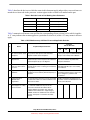
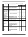
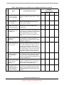
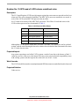
Freescale Semiconductor
Errata
Document Number: MPC7448CE
Rev. 6, 10/2008
Chip Errata for the
MPC7448
This document details all known silicon errata for the MPC7448. The MPC7448 is a microprocessor built
on Power Architecture™ technology. The MPC7450 has the same functionality as the MPC7448 and any
differences are detailed in the document. Table 1 provides a revision history for this chip errata document.
Table 1. Document Revision History
Revision
Date
Substantive Change(s)
6
10/2008
Added Erratum 26.
5
10/2007
Added Erratum 25.
4
05/2007
Added Erratum 23 and Erratum 24.
3
09/2006
Added Erratum 22.
Updated Projected Solution for Erratum 21.
2.1
03/2006
Clarified Erratum 21.
2
03/2006
Added Erratum 21.
1
02/2006
Added Erratum 18.
Added Erratum 19.
Added Erratum 20.
0
09/2005
Initial release.
© Freescale Semiconductor, Inc., 2008. All rights reserved.
Preliminary—Subject to Change Without Notice
Table 2 describes the devices to which the errata in this document apply and provides a cross-reference to
match the revision code in the processor version register to the revision level marked on the part.
Table 2. Revision Level to Part Marking Cross-Reference
MPC7448 Revision
Part Marking
Processor Version Register
1.0
A
0x8004_ 0100
2.0
B
0x8004_0200
2.1
C
0x8004_0201
2.2
D
0x8004_0202
Table 3 summarizes all known errata and lists the corresponding silicon revision level to which it applies.
A ‘Y’ entry indicates the erratum applies to a particular revision level, while a ‘N’ entry means it does not
apply.
Table 3. MPC7448 Summary of Silicon Errata and Applicable Revision
No.
Name
Errata in
Silicon Revision
Projected Impact Overview
1.0
2.0
2.1
2.2
1
Setting MSSCR0[18–24] Software that sets MSSCR0[18–24] bits will cause These bits have been marked ‘Reserved
will cause machine check the system to take spurious and sometimes
for factory use only’ in the MPC7450 RISC
frequent machine check exceptions.
exceptions
Microprocessor Family User’s Manual.
2
TAU reports incorrect
temperatures
3
The work around is documented in the
L2 hardware flush may not Data corruption will occur in systems whose
software misses in the iL1 during an L2 hardware MPC7450 RISC Microprocessor Family
flush every line from the
flush routine.
L2 cache
User’s Manual.
4
L1_TSTCLK must be
pulled low
The work around has been documented in
Tying L1_TSTCLK high may cause data
corruption in the L2 and may limit the frequency of the hardware specifications as the correct
way to configure L1_TSTCLK and
operation.
L2_TSTCLK.
5
Earliest transfer of
MPX/60x data
requirement
Any system where a device may assert TA or TEA The MPC7450 family implementation of
for a data tenure before or while the AACK for that the earliest transfer for MPX/60x data will
remain as documented.
transaction is driven.
6
Instructions following a
dcba mapped T = 1 may
not be executed
Any code that executes dcba instructions with
T = 1 effective addresses may not see all
instructions executed. Since Direct-Store
Segment Address Translation was originally
included in the architecture to support legacy
POWER architecture I/O devices that used this
interface, the impact to customers should be
minimal.
The TAU is not implemented as a feature
Programmed trip temperatures will not trigger
output interrupts, even if temperatures exceed the and is not included in any MPC7450
Family documentation.
expected setpoint by up to 55 degrees.
Y
Y
Y
Y
Chip Errata for the MPC7448, Rev. 6
2
Freescale Semiconductor
Preliminary—Subject to Change Without Notice
Table 3. MPC7448 Summary of Silicon Errata and Applicable Revision (continued)
No.
Name
Errata in
Silicon Revision
Projected Impact Overview
1.0
2.0
2.1
2.2
7
SRR0/SRR1/PC values
incorrectly updated if
instruction at breakpoint
in COP debug mode
causes an exception
Emulators that utilize the COP soft-stop feature
may not work as intended when attempting to set
a breakpoint at an instruction that causes an
exception.
Y
Y
Y
Y
8
Processor may hang
when mtmsr/isync
transitions MSR[IR] from
1->0 and isync instruction
resides in unmapped
page
Any systems that disable instruction translation
using mtmsr, and for which the required isync may
reside in a different page whose page table entry
is not available in the memory hierarchy may
hang.
Y
Y
Y
Y
9
Scanning MSS_NRM
chain via COP during
softstop may cause
unexpected interrupts
upon resumption of
normal operation
Emulators and debug tools accessing the
MSS_NRM scan chain via COP during softstop.
Y
Y
Y
Y
10 tlbie snoop during Doze
state may cause
processor hang
Systems performing tlbie snoops during Doze
state where the index of the tlbie matches that of
the instruction code that caused entry into Nap
mode may hang.
Y
Y
Y
Y
11 Data corruption due to
write-through aliasing in
the MMU
Systems performing write-through aliasing of the
same physical page may encounter data
corruption.
Y
N
N
N
12 HID0[SPD]=1 does not
prevent instruction fetches
past unresolved branches
when MSR[IR]=0
Systems executing code with instruction
translation disabled (MSR[IR]=0) and
HID0[SPD]=1 may see instruction fetches
propagate to the external bus unexpectedly.
Y
Y
Y
Y
13 SPR read of L3CR returns Any system expecting a read of the L3CR to return
undefined value
a result of zero due to the absence of the L3 cache
may receive a non-zero value instead. This may
cause some backwards compatibility issues with
existing system code that expects the value to be
zero if no L3 exists.
Y
Y
N
N
14 Store gathering/merging
performance issue
A software algorithm that performs multiple
back-to-back stores to the same cache line will
see a negative performance impact compared to
previous MPC744X/MPC745X processors.
Y
N
N
N
15 L2 latency performance
issue
Performance analysis of revision 1.0 of the
MPC7448 processor will encounter much higher
L2 latencies compared to the projected L2 latency
of this product.
Y
N
N
N
Chip Errata for the MPC7448, Rev. 6
Freescale Semiconductor
3
Preliminary—Subject to Change Without Notice
Table 3. MPC7448 Summary of Silicon Errata and Applicable Revision (continued)
No.
Name
Errata in
Silicon Revision
Projected Impact Overview
1.0
2.0
2.1
2.2
16 Unexpected instruction
fetch may occur when
transitioning MSR[IR]
0->1
Systems executing code as described above may
encounter unexpected machine checks or system
hangs.
Y
Y
Y
Y
17 Problem accessing
internal caches and
arrays via COP
This problem occurs on any system that uses a
COP emulator debugging tool to access the
internal caches and arrays.
Y
Y
Y
Y
18 Accessing LSRL via COP This problem occurs on any system that uses a
COP emulator to access the LSRL during
during soft stop mode
soft-stop mode.
causes data corruption
Y
Y
Y
Y
19 Processor I/O may lock up Any system with an affected device may
encounter this issue. Systems which adhere to the
during power-up, reset
power sequencing requirements described in the
and JTAG scan
MPC7448 RISC Microprocessor Hardware
Specifications have minimal vulnerability to this
issue.
Y
Y
N
N
20 Performance Monitor Out Systems designed to use the PMON_OUT signal
as an indication of an internal Performance
(PMON_OUT) not
Monitor event will not have this feature, originally
operational
intended as a debug aid.
Y
Y
Y
Y
Systems encountering this issue will typically fail
21 Back-to-back snoops to
L1 data cache may cause with a hang condition in which the processor will
enter an internal deadlock condition and cease to
processor hang
request the bus. Alternatively, it may enter an
external deadlock condition in which it will infinitely
retry all external bus snoops from other masters.
In the internal deadlock condition, decrementer
and timebase exceptions will not be serviced.
Y
Y
Y
N
22 Voltage Derating No
Longer Supported for
MC7448xx1700LC
devices
Operating MC7448xx1700LC at derated voltages
in not supported on devices with date code 0613
and later. Customers using MC7448xx1700LC
devices in the derated mode should migrate to the
MC7448xx1267NC device.
—
—
Y
Y
23 MCP or SRESET signal
assertion during transition
to Nap may hang
processor
Systems where MCP or SRESET can be asserted
during entry into Nap mode are at risk. The risk is
believed to be extremely small and has never
been observed in a MPC744X system.
Y
Y
Y
Y
24 Store type operations
during COP softstop
debug mode may hang
processor; Machine
check error limitations
Emulators that utilize the COP softstop feature
may not work as intended since the processor’s
violation of the system bus protocol may cause
unexpected behavior on the part of the system
controller.
Y
Y
Y
Y
Chip Errata for the MPC7448, Rev. 6
4
Freescale Semiconductor
Preliminary—Subject to Change Without Notice
Table 3. MPC7448 Summary of Silicon Errata and Applicable Revision (continued)
No.
Name
Errata in
Silicon Revision
Projected Impact Overview
1.0
2.0
2.1
2.2
25 Unpaired stwcx. may
hang processor
The processor will hang if the Load/Store Unit
does not report the completion of the stwcx. to the
Completion Unit. Paired lwarx/stwcx. instructions
are not affected by this erratum.
Y
Y
Y
Y
26 Using 7x and 14x PLL
multipliers may hang
system when exiting
HRESET state and nap,
sleep, COP softstop
modes
Systems using 60x bus mode and 7x multiplier
with SYSCLK > 100 MHz or 14x multiplier with
SYSCLK > 100 MHz are likely at risk of
encountering this erratum.
Systems using MPX bus mode and 7x multiplier
with SYSCLK > 100 MHz or 14x multiplier with
SYSCLK > 100 MHz and using MSSCR0[ABD] =
1 and MSSCR0[EIDIS] = 0 are at a low risk of
encountering this erratum when exiting from nap,
sleep and COP softstop modes.
Y
Y
Y
Y
Chip Errata for the MPC7448, Rev. 6
Freescale Semiconductor
5
Preliminary—Subject to Change Without Notice
Erratum No. 1: Setting MSSCR0[18–24] will cause machine check
exceptions
Description:
The MSSCR0 register fields 18–24, if not all zeros, can cause the MPC7450 to take a machine
check on internally triggered events without warning.
The MSSCR0 register fields 18–24 was originally intended for internal lab debug only. Setting one
or more of these bits can cause the MPC7450 to take machine checks (or a checkstop based on
MSR[ME]) due to unspecified internal events. These events, while useful for initial internal lab
debug, have ceased to be of value and may cause undesired system behavior if set.
Projected Impact:
Software that sets MSSCR0[18–24] bits will cause the system to take spurious and sometimes
frequent machine check exceptions.
Work-Around:
Do not set MSSCR0[18–24].
Projected Solution:
These bits have been marked “Reserved for factory use only” in the MPC7450 RISC
Microprocessor Family User’s Manual.
Chip Errata for the MPC7448, Rev. 6
6
Freescale Semiconductor
Preliminary—Subject to Change Without Notice
Erratum No. 2: TAU reports incorrect temperatures
Description:
The thermal assist unit (TAU) on the MPC7450 and MPC7455 reports temperatures between 35 to
55 degrees lower than expected.
This erratum effects only customers using the TAU. If a trip temperature is programmed into the
sensor’s control registers, the output interrupt is never received, even if temperatures exceed the
expected setpoint by up to 55 degrees (even after calibration). A control application will not be
alerted of excessive temperatures and this could lead to damage of the part.
Projected Impact:
Programmed trip temperatures will not trigger output interrupts, even if temperatures exceed the
expected setpoint by up to 55 degrees.
Work-Around:
None
Projected Solution:
None. The TAU is not implemented on the MPC7448.
Chip Errata for the MPC7448, Rev. 6
Freescale Semiconductor
7
Preliminary—Subject to Change Without Notice
Erratum No. 3: L2 hardware flush may not flush every line from the L2 cache
Description:
A valid line in the L2 may be ignored during an L2 hardware flush if instruction fetches are trying
to allocate into the L2 during the flush.
The MPC7450 performs ‘front-end’ allocation in the L2 cache. If a request misses in the L2, the
L2 allocates an entry at the time of the miss to make room for the subsequent reload by setting an
‘allocated’ bit in the L2 cache status for that line. This bit is cleared when the reloaded data is
received.
The L2 hardware flush mechanism sequentially performs a tag read on every index, sector, and way
in the L2 tag. As it encounters a valid entry, an operation is queued to the L2 to either simply
invalidate the line or push the data from the cache if the data is modified.
The failing scenario is as follows: an instruction access to address ‘A’ from the L1 instruction cache
(iL1) accesses and misses in the L2. The alternate sector for address ‘A’ is currently allocated in
the L2 in way ‘N’ and awaiting a reload from the L3 or external bus. Meanwhile, the victim
selection logic has chosen way ‘N’ to evict from the cache if an eviction is necessary. Since address
‘A’ alternate sector is in way ‘N,’ no eviction is necessary. The miss for ‘A’ queues up an internal
allocate request to the L2 to allocate into way ‘N.’ During the cycle in which the instruction
allocate request arbitrates into the L2, an L2 hardware flush to an unrelated index/sector/way
‘X/Y/Z’ is also arbitrating into the L2. Normally, the allocate request would win. As a result, an
internal address mux that chooses the address with which to access the L2 is selected as the allocate
address ‘A.’ However, an under-qualified internal retry condition exists for the allocate, where if
the victim selection logic points to a way in which the alternate sector is in the allocated state,
which it is, then the new allocate request gets retried. In this failing scenario, the L2 hardware flush
request wins, since the allocate request gets retried. Meanwhile, the address mux continues to
select the allocate address ‘A.’ As a result, the L2 hardware flush routine moves on to the next L2
tag entry without having accessed the current index/sector/way ‘X/Y/Z.’
Projected Impact:
Data corruption will occur in systems whose software misses in the iL1 during an L2 hardware
flush routine.
Work-Around:
Set the IONLY and DONLY bits in the L2CR prior to the L2 hardware flush.
Projected Solution:
The work around has been documented in the MPC7450 RISC Microprocessor Family User’s
Manual as the correct way to flush the L2 cache.
Chip Errata for the MPC7448, Rev. 6
8
Freescale Semiconductor
Preliminary—Subject to Change Without Notice
Erratum No. 4: L1_TSTCLK must be pulled low
Description:
Early revisions of the MPC7450 RISC Microprocessor Hardware Specifications incorrectly
recommended pulling up L1_TSTCLK.
On all previous parts, L1_TSTCLK has been identified as a factory test pin and is recommended
to be pulled high. This historical precedent was perpetuated in the MPC7450 RISC Microprocessor
Hardware Specifications. However, on the MPC7450 Rev. 2.0, pulling this pin high prevents
proper operation of the L2 cache and may limit the maximum frequency.
The MPC7450 RISC Microprocessor Family User’s Manual does not address L1_TSTCLK or
L2_TSTCLK.
Revision 1 and prior of the MPC7450 RISC Microprocessor Hardware Specifications notes these
signals are test input signals for factory use only and must be pulled up to OVDD for normal
machine operation.
Projected Impact:
Tying L1_TSTCLK high may cause data corruption in the L2 and may limit the frequency of
operation.
Work-Around:
Tie L1_TSTCLK low for proper device operation. It is recommended that L2_TSTCLK be tied to
HRESET, but other configurations will not adversely affect performance.
Projected Solution:
Documented correctly in all the MPC7450 family hardware specifications.
Chip Errata for the MPC7448, Rev. 6
Freescale Semiconductor
9
Preliminary—Subject to Change Without Notice
Erratum No. 5: Earliest transfer of MPX/60x data requirement
Description:
The MPC7450 does not support the transfer of any data on MPX/60x bus before the processor’s
snoop response window, defined as the cycle after AACK is asserted.
The MPC7450 implementation of the earliest transfer of data during an MPX/60x bus transaction
is more restrictive than previous processors including the MPC7400/MPC7410. This
implementation creates a backwards compatibility issue with older system chipsets, including the
Tundra Tsi106™ PowerPC host bridge or the Tundra Tsi107™
host bridge revisions prior to Rev. 1.4. In addition, any newly designed chipsets must adhere to this
restriction.
In an MPC7450 system, the system chipset logic must ensure that the last (or only) assertion of TA
for a data transfer does not occur sooner than the last cycle of the snoop response window (cycle
after AACK). Note that DBG can still be driven as early as TS. Likewise, the system chipset logic
must ensure that TEA is not asserted before the last cycle of the snoop response window.
The Tsi106 host bridge and the Tsi107 host bridge prior to Rev. 1.4 may transfer read and write
data with the processor ending at or before the cycle of AACK, which is one cycle before that
permitted by the MPC7450. Systems that include either of these two bridge devices, or devices
with the same behavior, are susceptible to processor hangs or data corruption as a result of this
issue.
Projected Impact:
Any system where a device may assert TA or TEA for a data tenure before or while the AACK for
that transaction is driven.
Work-Around:
Devices must not assert TA or TEA for a transaction before that transaction’s snoop response
window (cycle after AACK), as documented in the MPC7450 RISC Microprocessor Family User’s
Manual.
Projected Solution:
The MPC7450 implementation of the earliest transfer for data is as documented in the MPC7450
RISC Microprocessor Family User’s Manual.
Chip Errata for the MPC7448, Rev. 6
10
Freescale Semiconductor
Preliminary—Subject to Change Without Notice
Erratum No. 6: Instructions following a dcba mapped T = 1 may not be
executed
Description:
A single instruction that is one, two, or three instructions following a dcba instruction with an
address mapped using Direct-Store Segment Address Translation (T = 1) may not be executed.
Direct-Store Segment Address Translation has been removed from the architecture and is not
supported on the MPC750, MPC7400, or MPC7450 processors. However, the following cache
operations, when mapped T = 1, should still no-op as defined in the original architecture: dcba,
dcbz, icbi, dcbst, dcbi, dcbf, dcbtst, and dcbt.
On the MPC7450, the dcba instruction will correctly no-op when T = 1, but will incorrectly cause
subsequent instructions to not be executed. Specifically, one of the instructions in a window of
three instructions immediately following the dcba may not be executed. All three instructions may
be executed correctly, but a maximum of one may not be executed. Whether or not this one
instruction is executed is highly dependent upon internal timings.
Note that if branch folding is enabled (HID0[FOLD] = 1), and one or multiple branch instructions
following the dcba are folded, then these branch instructions do not count towards determining the
window of three instructions following the dcba.
Projected Impact:
Any code that executes dcba instructions with T = 1 effective addresses may not see all
instructions executed. Since Direct-Store Segment Address Translation was originally included in
the architecture to support legacy POWER architecture I/O devices that used this interface, the
impact to customers should be minimal.
Work-Around:
A work around can be achieved by doing one of the following:
1. Do not map dcba instructions to T = 1 space.
2. Follow each dcba with three no-op instructions.
3. Follow each dcba instruction with an isync instruction.
Projected Solution:
None. This erratum will not be fixed in any subsequent revisions of the MPC7450 family.
Chip Errata for the MPC7448, Rev. 6
Freescale Semiconductor
11
Preliminary—Subject to Change Without Notice
Erratum No. 7: SRR0/SRR1/PC values incorrectly updated if instruction at
breakpoint in COP debug mode causes an exception
Description:
During softstop debug mode, which is accessible through the COP, the processor corrupts the
values of the SRR0/SRR1/PC if an instruction that matches IABR causes an exception of lower
priority than a breakpoint exception.
If the instruction address breakpoint register (IABR) is set and enabled for an instruction address
in COP softstop mode, the processor should halt operation and stop internal clocks before the
instruction is executed. The PC should point to that instruction’s address.
However, the processor may incorrectly update the PC if the instruction at that address causes an
exception of lower priority than an IABR breakpoint. The SRR0 is incorrectly updated to the
address of the instruction itself, and the SRR1 is modified.
For example, if the IABR points to an instruction that performs a data access to an address space
that is mapped no-access in a DBAT, the PC is updated to the DSI exception handler address, and
the SRR0 is updated to the address of the excepting instruction.
Other exception types that cause this failure are illegal instruction exceptions, traps, floating-point
or Altivec unavailable exceptions, privilege violations, and alignment exceptions.
Data translation that hits in the on-chip DTLB as an access violation will also show this problem.
Translation that misses in the DTLB and requires a tablewalk will not show this problem because
the tablewalk will be correctly terminated before any page table results return.
Instruction address breakpoints set through software during normal functional mode stop correctly
before any PC/SRR0/SRR1 update occurs.
Projected Impact:
Emulators that utilize the COP soft-stop feature may not work as intended when attempting to set
a breakpoint at an instruction that causes an exception.
Work-Around:
None.
Projected Solution:
Under review.
Chip Errata for the MPC7448, Rev. 6
12
Freescale Semiconductor
Preliminary—Subject to Change Without Notice
Erratum No. 8: Processor may hang when mtmsr/isync transitions MSR[IR]
from 1->0 and isync instruction resides in unmapped page
Description:
If the mtmsr instruction is used to disable instruction translation, and the subsequent isync
instruction resides on a different page than the mtmsr instruction, and the isync instruction’s page
causes a page fault exception, the processor will hang before taking the page fault exception. Once
in the hang state, the processor will not recover and hard reset must be asserted.
An alternate failing scenario can exist if the mtmsr and isync reside on the same page but in
different quadwords. If the mapping for that page exists in the iTLB, but not the page table, and a
tlbie snoop occurs between the mtmsr and isync that invalidates the iTLB entry, then the processor
will hang before taking the page fault exception.
If the isync instruction address is guaranteed to have a valid page table mapping resident in the
memory hierarchy, then neither scenario can occur.
Projected Impact:
Any systems that disable instruction translation using mtmsr, and for which the required isync
may reside in a different page whose page table entry is not available in the memory hierarchy
may hang.
Any systems mapping the mtmsr/isync code with the IBATs will not fail due to this issue. Any
systems not demand-paging their supervisor-level code will not fail due to this issue.
Work Arounds:
Any of the following work-arounds will avoid the processor hang:
• mtmsr/isync instruction pairs should reside within the same quadword.
• disable instruction translation by initializing SRR0/SRR1 and executing rfi.
• map code which disables instruction address translation with the IBATs.
Projected Solution:
Under review.
Chip Errata for the MPC7448, Rev. 6
Freescale Semiconductor
13
Preliminary—Subject to Change Without Notice
Erratum No. 9: Scanning MSS_NRM chain via COP during softstop may
cause unexpected interrupts upon resumption of normal
operation
Description:
If the MSS_NRM scan chain is accessed via COP during softstop and MSR[EE] is set, then an
unexpected decrementer (0x0900) or thermal management (0x1700) interrupt may occur when the
processor resumes from softstop.
The following special purpose registers reside in the MSS_NRM scan chain:
1. HID1
2. L2CR
3. L3CR/L3PM/L3ITCR[0-3]/L3OH (L3ITCRs[1-3]/L3OH exist in MPC7457 only)
4. MSSCR0
5. MSSSR0
6. TBL/TBU
7. DEC
8. THRM1/THRM2/THRM3 (exist in MPC7451/MPC7445/MPC7455 only)
Accessing any of the above registers may trigger the unexpected interrupt.
The unexpected thermal management interrupt will only occur in the MPC7451 and MPC7455
processors.
The unexpected decrementer interrupt may occur in all processors of the MPC7450 family.
Projected Impact:
Emulators and debug tools accessing the MSS_NRM scan chain via COP during softstop.
Work Arounds:
Use LSRL to access any elements in the MSS_NRM scan chain including the SPRs listed above.
Projected Solution:
Under review.
Chip Errata for the MPC7448, Rev. 6
14
Freescale Semiconductor
Preliminary—Subject to Change Without Notice
Erratum No. 10:tlbie snoop during Doze state may cause processor hang
Description:
If the instruction TLB entry for the code that caused entry into Nap mode is invalidated while in
Doze state via a snooped tlbie, an instruction tablewalk will be immediately triggered for that
instruction address. Taking the tablewalk is an incorrect action for the processor because no code
is being executed during Doze state.
A processor hang can occur due to the unintentional tablewalk if the tablewalk results in an ISI
exception, most likely due to a page fault. When the page fault is detected, the SRR0, SRR1, and
MSR registers are updated as for a normal ISI exception except that the ISI handler code is not
fetched because of the Doze state. Since the MSR[EE] External Interrupt Enable bit is cleared due
to the ISI exception, neither an external interrupt or a decrementer interrupt can wake the processor
from Nap mode. A processor hang results.
If the unintentional instruction hardware tablewalk had completed without an exception, the
MSR[EE] bit would not be cleared and the processor can be woken from Nap mode by an interrupt.
However, system designers should use caution since the processor is only ever expected to provide
snoop responses and/or push or intervention data during Doze state. Due to the unintentional
tablewalk, up to four tablewalk read requests may occur to the external bus. The system would
either have to service these read requests before re-entering Nap mode, or somehow ignore pending
bus request assertions for these reads.
Projected Impact:
Systems performing tlbie snoops during Doze state where the index of the tlbie matches that of
the instruction code that caused entry into Nap mode may hang.
Systems using the iBATs to map the Nap mode code are not affected.
Since a tlbie snoop will only likely occur in multiprocessor systems, most uniprocessor systems
should not be affected.
Work Arounds:
Any of the following work arounds are acceptable:
1. Do not perform tlbie snoops during Doze state
2. Disable instruction address translation before entering Nap mode.
3. Map the code that causes entry into Nap mode using the IBATs.
4. Ensure that the page table entry mapping for the Nap mode code remains valid during Nap
mode, perhaps via an OS locking mechanism. Note that the system would still have to handle
potential tablewalk read accesses during Doze state.
Projected Solution
Under review.
Chip Errata for the MPC7448, Rev. 6
Freescale Semiconductor
15
Preliminary—Subject to Change Without Notice
Erratum No. 11:Data corruption due to write-through aliasing in the MMU
Description:
If the memory management unit (MMU) on the MPC7450 processor is programmed such that the
same physical block or page has storage access attributes mapped as both cacheable in one memory
mapping and write-though in another, data corruption may result.
Accesses to the same storage location using two effective addresses for which the write-through
mode (W-bit) differs meet the memory coherence requirements of a MPX744X processor if the
accesses are performed by a single processor. Since the usage of the W-bit is mixed for the same
physical address, a store addressed to a write-through page may find the addressed cache block
modified in either the dL1 or L2 caches. In this case, the write-through store will update the
location in both the cache block and main storage. The cache block remains in the modified state.
If a block or page is mapped as write-though only, the cache line will never be modified.
In the failing scenario, address “A”, which is mapped both as cacheable and write-through resides
as modified in the dL1 cache. A unrelated dL1 reload to the same set as address “A” occurs. The
reload chooses address “A” for eviction due to the pseudo-LRU replacement algorithm. As a
castout is being created of address “A”, a write-though store to address “A” erroneously bypasses
the castout without updating the data. As a result, the castout with stale data will be written to
memory after the write-through store.
Projected Impact:
Systems performing write-through aliasing of the same physical page may encounter data
corruption.
Work Arounds:
Do not permit two effective addresses to map to the same physical address where one effective
address is mapped as write-though and the other is mapped as cacheable. If write-through aliasing
is unavoidable, the dL1 cache must be flushed of its contents by the system when switching from
cacheable to write-through accesses.
Projected Solution:
Fixed in Rev 2.0.
Chip Errata for the MPC7448, Rev. 6
16
Freescale Semiconductor
Preliminary—Subject to Change Without Notice
Erratum No. 12:HID0[SPD]=1 does not prevent instruction fetches past
unresolved branches when MSR[IR]=0
Description:
An out-of-order instruction fetch is defined as an instruction fetch made before it is known whether
the instructions are required by the sequential execution model. When instruction translation is
disabled (MSR[IR]=0), the accesses are guarded. In general, guarded storage is not accessed
out-of-order. Three exceptions to this rule, as defined by the architecture, may cause out-of-order
instruction fetches:
1. The instruction is in the instruction cache.
2. The instruction resides in the same physical page as an instruction that is required by the
execution model.
3. The instruction resides in the next sequential physical page after the page of an instruction that
is required by the execution model.
Therefore, guarded out-of-order instruction fetches may occur to a page for which there are no
executable instructions as long as the previous page contained instructions required by the
sequential execution model.
Typically, system software will contain a branch near the end of the second to last page of a
memory region and leave the last page empty but valid. For example, a hypothetical system with
one megabyte of memory will place no executable code in the last 4096 bytes of the one megabyte
of memory space to avoid instruction fetches on the external bus interface beyond the one
megabyte of valid physical memory.
The HID0[SPD], “Speculative data cache and instruction cache access disable”, is designed to
prevent out-of-order instruction cache fetches beyond an unresolved branch and into a subsequent
page from propagating to the external bus interface. By definition, setting HID0[SPD]=1 should
permit a final branch instruction to exist in the very last word of a physical memory region.
However, the MPC7450 processor with HID0[SPD]=1 will incorrectly fetch past an unresolved
branch as with HID0[SPD]=0, and perhaps create an external bus read operation to an invalid
region of memory.
HID0[SPD] works as designed for load operations.
Projected Impact:
Systems executing code with instruction translation disabled (MSR[IR]=0) and HID0[SPD]=1
may see instruction fetches propagate to the external bus unexpectedly.
Work Arounds:
System software should not place the last branch instruction at the end of a physical memory region
in the last two cache lines of that memory region when MSR[IR]=0 and HID0[SPD]=1. If the
branch is placed in the third to last cache line, accesses may still occur to the external bus for the
final two cache lines, but no accesses will occur to the subsequent page.
The same restriction actually also holds when HID0[SPD]=0. Although architecturally the
processor is permitted to access instructions out-of-order and into the next page past what is
Chip Errata for the MPC7448, Rev. 6
Freescale Semiconductor
17
Preliminary—Subject to Change Without Notice
required by the sequential execution model, the processor will not do so if the final branch is not
in the last two cache lines of the last page required by the sequential execution model.
Projected Solution:
Under review.
Chip Errata for the MPC7448, Rev. 6
18
Freescale Semiconductor
Preliminary—Subject to Change Without Notice
Erratum No. 13:SPR read of L3CR returns undefined value
Description:
The L3 Control Register (L3CR) special purpose register does not return an expected result of zero
when read. The value returned is undefined. The MPC7447A processor returned a zero result. A
write of the L3CR on the MPC7448 processor has no effect.
No L3 cache exists on any of the MPC744X processors. The effects of reads and writes to the
L3CR on these processors are documented in Table 4.
Table 4. L3CR Read and Write Effects
Processor
L3CR Write Actions
L3CR Read Result
MPC7448
None
undefined
MPC7447A
None
zero
MPC7447
L3CR register updated
last value written
MPC7445
L3CR register updated
last value written
MPC7441
L3CR register updated
last value written
Although the L3CR registers of the MPC7441/MPC7445/MPC7447 processors can be read and
written, with the read returning the last value written, the write had no other functional effect since
the L3 cache does not exist.
Projected Impact:
Any system expecting a read of the L3CR to return a result of zero due to the absence of the L3
cache may receive a non-zero value instead. This may cause some backwards compatibility issues
with existing system code that expects the value to be zero if no L3 exists.
Work Arounds:
The L3CR should be treated as an unimplemented SPR that returns an undefined result when read.
Projected Solution:
Under review.
Chip Errata for the MPC7448, Rev. 6
Freescale Semiconductor
19
Preliminary—Subject to Change Without Notice
Erratum No. 14:Store gathering/merging performance issue
Description:
To increase external bandwidth to frame buffers and I/O devices, the MPC7448 performs store
gathering of unguarded write-through stores or cache-inhibited stores. The same store gathering
mechanism is used to merge cacheable write-back stores. This feature is enabled by setting
HID0[SGE].
The stores are gathered/merged while in the 5-entry committed store queue (CSQ). The basic rule
is gathering/merging can occur if cache line addresses in CSQn and CSQn+1 match, and CSQn is
not potentially gathering/merging with CSQn-1. Gathering/merging never occurs between CSQ0
and CSQ1. (For the complete set of requirements please refer to Section 3.1.2.3, “Store
Gathering/Merging,” in the MPC7450UM)
However, on the MPC7448 processor, if CSQ0 and CSQ1 are to the same cache line, CSQ2 is
incorrectly signalled that CSQ1 may potentially be gathering/merging with CSQ0, even though
gathering/merging is never allowed with CSQ0. As a result, gathering/merging will be blocked
between CSQ2 and CSQ1. This may cause a ripple effect of blocked gathering/merging between
CSQ2/CSQ3 and CSQ3/CSQ4 depending on the addresses of the stores.
This issue will not cause a functional fail.
Projected Impact:
A software algorithm that performs multiple back-to-back stores to the same cache line will see a
negative performance impact compared to previous MPC744X/MPC745X processors.
Work Arounds:
None.
Projected Solution:
Fixed in Rev 2.0.
Chip Errata for the MPC7448, Rev. 6
20
Freescale Semiconductor
Preliminary—Subject to Change Without Notice
Erratum No. 15:L2 latency performance issue
Description:
In revision 1.0 of the MPC7448 processor memory subsystem pipeline, the total latency for L1 data
and instruction cache misses that hit in the L2 is greater than the documented projected latency.
The documented L2 latency with ECC disabled for data is 11 cycles and, for instructions, is 15
cycles. The documented L2 latency with ECC enabled for data is 12 cycles and, for instructions, is
16 cycles.
The actual L2 latency with ECC disabled for data is 14 cycles and, for instructions, is 18 cycles.
The actual L2 latency with ECC enabled for data is 15 cycles and, for instructions, is 19 cycles. An
L2 latency as high as 21 cycles (data) has been observed for some applications with ECC enabled.
Projected Impact:
Performance analysis of revision 1.0 of the MPC7448 processor will encounter much higher L2
latencies compared to the projected L2 latency of this product.
Work Arounds:
None.
Projected Solution:
Fixed in Rev 2.0.
Chip Errata for the MPC7448, Rev. 6
Freescale Semiconductor
21
Preliminary—Subject to Change Without Notice
Erratum No. 16:Unexpected instruction fetch may occur when transitioning
MSR[IR] 0->1
Description:
An mtmsr/isync pair followed by a blr, bctr, or branch absolute instruction, where the target
effective address is not equal to the target physical address, may cause an unexpected instruction
fetch on the MPX or 60x bus using the effective address.
The effect of the unexpected instruction fetch will be system dependent. If physical memory exists
at the unexpected address, and read accesses are permitted, the processor will simply discard any
returned instructions after the data tenure is complete, and no fail will occur. If a TEA_ is asserted
for the data tenure
the processor will take either an unexpected machine check exception or checkstop.
The unexpected instruction fetch issue is independent of translation method, and thus can occur for
either iBATs or page tables.
Projected Impact:
Systems executing code as described above may encounter unexpected machine checks or system
hangs.
Work Arounds:
The recommended work around is for any target of an unconditional branch in the sixteen
instructions following an mtmsr/isync pair where instruction translation is being enabled to have a
translation mapping of effective address = physical address.
If such a mapping is not possible, the issue can be avoided if the effective address target matches
a valid region of physical memory in the system. As with the previous work around, the unexpected
instruction fetch would still occur, and the instructions would be discarded by the processor.
A third work around is to only enable instruction translation by initializing SRR0/SRR1 and
executing rfi. A fourth work around that would prevent the unexpected fetch altogether would be
to guarantee in software that there were no unconditional branches in the sixteen instructions
following the mtmsr/isync pair.
Projected Solution:
Under review.
Chip Errata for the MPC7448, Rev. 6
22
Freescale Semiconductor
Preliminary—Subject to Change Without Notice
Erratum No. 17:Problem accessing internal caches and arrays via COP
Description:
COP emulator debugging tools cannot read the internal caches and arrays reliably at high speed.
Additionally, emulator debugging tools cannot write to internal caches and arrays reliably at any
speed.
Projected Impact:
This problem occurs on any system that uses a COP emulator debugging tool to access the
internal caches and arrays.
Work Arounds:
When reading the internal caches and arrays, the COP emulator can slow down the core frequency
using the DFS (dynamic frequency switching) whenever it tries to read the internal caches and
arrays. This process should be transparent to the end user if the tool vendor implements the work
around.
When writing the internal caches and arrays, the COP emulator should attempt to write the data
multiple times until the data is correctly written to the part. This process should be transparent to
the end user if the tool vendor implements the work around.
Projected Solution:
Under review.
Chip Errata for the MPC7448, Rev. 6
Freescale Semiconductor
23
Preliminary—Subject to Change Without Notice
Erratum No. 18:Accessing LSRL via COP during soft stop mode causes
data corruption
Description:
Accessing LSRL via COP emulators during soft stop mode can cause LSRL data corruption. LSRL
corruption can occur if COP emulator tool accesses the LSRL during soft stop mode.
Emulator tools use soft-stop regularly for debugging purposes. The tool emulators use soft-stop in
the following cases:
1. To stop the execution of a user program.
2. To single step user program.
3. To set up an instruction breakpoint in the user program.
4. To set up a data breakpoint in the user program.
All of the above actions cause the processor to go into a stop mode, assuming that the breakpoint
in (3) or (4) is hit. If the COP emulator tool accesses the LSRL during soft stop, the system can
hang after resuming.
Projected Impact:
This problem occurs on any system that uses a COP emulator to access the LSRL during soft-stop
mode.
Work Arounds:
The COP emulator should turn off the warm-up clock during HRESET assertion. This process
should be transparent to the end user if the tool vendor implements the work around.
Projected Solution:
Under review.
Chip Errata for the MPC7448, Rev. 6
24
Freescale Semiconductor
Preliminary—Subject to Change Without Notice
Erratum No. 19:Processor I/O may lock up during power-up, reset and JTAG
scan
Description:
The I/O buffers may be erroneously disabled at power-up, during reset, or during JTAG scan,
causing processor to lock up.
In the most common occurrence of this issue, control circuits for the I/O buffers may be placed in
an incorrect state upon power up, causing the buffers to be disabled. As a result, the processor
hangs and cannot recover until power is cycled. In rare cases, it is also possible to cause such a
hang during JTAG scan operations. It may be possible for the part to lock up during a (non-POR)
device reset, though this has never been observed within the nominal operating conditions
described in the MPC7448 RISC Microprocessor Hardware Specifications.
The lock-up condition can only be encountered during power-up, reset, and JTAG scan operations,
and will not be encountered during normal device operation.
Projected Impact:
Any system with an affected device may encounter this issue. Systems which adhere to the power
sequencing requirements described in the MPC7448 RISC Microprocessor Hardware
Specifications have minimal vulnerability to this issue.
Work Arounds:
Implementing the following measures will minimize the chances of lock-up during power-up:
1. Adherence to the power sequencing requirements described in the MPC7448 RISC
Microprocessor Hardware Specifications.
2. HRESET signal asserted while VDD and OVDD ramp up.
3. TRST signal asserted while VDD and OVDD ramp up.
No known work arounds exist for lock-up during JTAG scan or device reset, but the likelihood of
encountering this issue in these cases is believed to be very rare.
Projected Solution:
Fixed in Rev 2.1.
Chip Errata for the MPC7448, Rev. 6
Freescale Semiconductor
25
Preliminary—Subject to Change Without Notice
Erratum No. 20:Performance Monitor Out (PMON_OUT) not operational
Overview:
The Performance Monitor Out output signal on the MPC7450 will not be asserted by the
Performance Monitor unit as expected. PMON_OUT is defined to be asserted on the external
interface when either a PMCn register overflow condition or a timebase event occurs. However,
when either condition is detected, the processor incorrectly drops the event in most cases.
Projected Impact:
Systems designed to use the PMON_OUT signal as an indication of an internal Performance
Monitor event will not have this feature, originally intended as a debug aid.
Work Arounds:
No known general work around exists for this erratum.
The following two examples are the only known work arounds and are specific to 6:1 and 8:1
processor: bus ratios and the timebase unit.
In 6:1 processor:bus ratio, a time-base event with MMCR0[TBSEL]=00 (TBL[31]) can be used to
force PMON_OUT to be asserted. PMON_OUT in this case would be asserted maximum once
every eight system clocks.
In 8:1 processor:bus ratio, an overflow condition of event PMC1-4[3] with MMCR0[TBSEL]=00
(TBL[31]) can be used to force PMON_OUT to be asserted.
Projected Solution:
Under review.
Chip Errata for the MPC7448, Rev. 6
26
Freescale Semiconductor
Preliminary—Subject to Change Without Notice
Erratum No. 21:Back-to-back snoops to L1 data cache may cause processor
hang
Overview:
Two sources of snoops can access the L1 data cache: external snoops from the 60x/MPX bus and
internal snoops initiated by the processor. Due to an issue with the MPC7448 processor, an external
snoop request followed by an internal snoop request (or vice-versa) in back-to-back processor
clocks to the same modified dL1 cache line may cause the second of two snoops to receive an
incorrect MESI state from the L1 data cache. A processor hang may result.
Internal snoop requests can be generated by load requests from the L2 hardware prefetch engine
and instruction fetch requests, both of which snoop the dL1. These requests are initiated and
performed internally and are not visible on the external 60x/MPX bus.
If the L2 hardware prefetch engine is enabled, a prefetch internal snoop can collide with an external
snoop and a failure may result. Not enabling the L2 hardware prefetch engine eliminates this source
of internal dL1 snoop requests and will prevent this failure mode from occurring.
The sequencer unit of the processor will speculatively fetch instructions past the currently
executing instructions. Unless properly constrained via software, these instruction fetches are
architecturally permitted to fetch into data regions. If this data is cached as modified in the dL1,
then the instruction fetch snoop and the external snoop to the modified cache line can occur
back-to-back and cause the processor to hang.
Projected Impact:
Any system in which L2 hardware prefetching is enabled may be impacted by this erratum.
Additionally, systems in which all of the following conditions occur are susceptible to this
erratum:
1. Address mapping in the instruction MMU (IMMU) is such that one or more IBATs or PTEs are
mapped to physical address ranges in which data resides
2. Data in these physical address regions may exist in the modified state in the dL1
3. The system generates snoop activity to the above physical addresses ranges
Systems that have L2 hardware prefetching disabled and do not meet all three of the above criteria
are not susceptible to this issue.
For systems that do meet all three criteria, two sources of potential failure exist due to out-of-order
instruction fetching:
1. Sequential fetching ahead of the currently executing instruction stream.
2. Speculative execution of bcctr or bclr instructions.
If instructions and data are separated such that they do not reside within six cache lines of each
other then source No. 1 is not a concern. If bcctr or bclr instructions exist in the instruction
stream, source No. 2 exists regardless of the separation between instructions and data.
However, it must be noted that for the failure to occur, three specific events must coincide:
1. A bcctr or bclr instruction is speculatively executed which causes the instruction stream to
begin fetching from addresses in a data region
Chip Errata for the MPC7448, Rev. 6
Freescale Semiconductor
27
Preliminary—Subject to Change Without Notice
2. The data at the fetched address must be modified in the dL1
3. The system must generate an external snoop to the same address in the same cycle as the
instruction fetch request
Because failure requires all three events to occur with specific timing, and because in nearly all
instances the LR and CTR will point to areas of memory containing instructions, the likelihood of
encountering this issue as a result of a speculatively executed bcctr or bclr instruction is very
small, but not zero.
Systems encountering this issue will typically fail with a hang condition in which the processor
will enter an internal deadlock condition and cease to request the bus. Alternatively, it may enter
an external deadlock condition in which it will infinitely retry all external bus snoops from other
masters. In the internal deadlock condition, decrementer and timebase exceptions will not be
serviced.
Work Arounds:
L2 hardware prefetching must be disabled (MSSCR0[L2PFE] = 0). (Note: this is the default
setting.) This will prevent internal snoops caused by L2 prefetches.
To prevent the internal snoops due to instruction fetches from causing a failure, it must be
guaranteed that instruction fetches, when snooping the dL1, do not encounter modified data in the
dL1 for the address of the instruction being snooped if the system may generate external snoops to
that same address. The following measures will guarantee this will not occur:
1. Data and instructions must reside in different physical pages of memory. Since hardware and
software tablewalks do not occur speculatively, this prevents instructions from snooping the
dL1 with an address shared by the data region.
2. Instruction block address translation registers (IBATs) must not overlap into regions in which
data, mapped either by page tables or DBATs, is stored as modified. Mapping DBATs such that
they overlap into instruction regions is acceptable as long as the data in the overlapping region
is flushed from the dL1 (if modified) before instructions are fetched.
3. The work arounds listed in MPC7448 Errata No. 12 and No. 16 must be followed.
If measure No. 2 is unacceptable, then an alternative is to maintain a separation of two cache lines
between instructions and data in these IBAT regions and operate with either MSR[IR]=0 or
HID0[SPD]=1.
Projected Solution:
Fixed in Rev 2.2.
Chip Errata for the MPC7448, Rev. 6
28
Freescale Semiconductor
Preliminary—Subject to Change Without Notice
Erratum No. 22:Voltage Derating No Longer Supported for
MC7448xx1700LC devices
Overview:
To reduce power consumption, MC7448xx1700LC devices previously supported voltage and
frequency derating in which the core voltage (VDD) could be reduced if the reduced maximum
processor core frequency requirements were observed. This feature has been made redundant by
new device offerings and is no longer supported.
For archival purposes, the supported derated core voltage, resulting maximum processor core
frequency (fcore), and power consumption are provided in Table 5. Only those parameters in
Table 5 were affected; all other parameter specifications were unaffected. Note that only
MC7448xx1700LC devices previously supported this feature, and it was not supported for any
other speed grades of the MC7448xxnnnnLC devices.
Table 5. Supported Voltage, Core Frequency, and Power Consumption Derating (MC7448xxnnnnLC)1
1
2
Maximum Rated
Core Frequency
(Device Marking)
Date Code2
Supported
Derated Core
Voltage (VDD)
1700
0612 and prior
1.0 V ± 50 mV
Maximum Derated Full-Power Mode Power Consumption
Core Frequency
(fcore)
Typical
Thermal
Maximum
1250 MHz
8.4 W
0613 and later
N/A
1600
All
N/A
1420
All
N/A
1000
All
N/A
10.3 W
12.0 W
This feature is no longer supported.
See Section 11.3, “Part Marking,” in the MPC7448 RISC Microprocessor Hardware Specifications for information
regarding date codes and part marking.
Projected Impact:
Operating MC7448xx1700LC at derated voltages in not supported on devices with date code
0613 and later. Customers using MC7448xx1700LC devices in the derated mode should migrate
to the MC7448xx1267NC device.
See the MPC7448 RISC Microprocessor Hardware Specifications for information on date codes
and device markings.
Work Arounds:
Customers desiring the power savings provided by voltage and frequency derating are referred to
the MC7448xxnnnnNx series of part numbers. See the MPC7448 RISC Microprocessor Hardware
Specifications for more information.
Projected Solution:
None. This erratum is for advisory purposes only. Freescale will continue to support customers
requiring low-power devices via the MC7448xxnnnnNx series.
Chip Errata for the MPC7448, Rev. 6
Freescale Semiconductor
29
Preliminary—Subject to Change Without Notice
Erratum No. 23:MCP or SRESET signal assertion during transition to Nap
may hang processor
Overview:
If the machine check signal (MCP) or soft reset signal (SRESET) are asserted in a window after
MSR[POW] has been set but before the processor has asserted the quiesce request signal (QREQ),
then the processor may encounter a hang condition.
The nap entry sequence in the MPC74XX User’s Manual is as follows:
loop: sync
mtmsr POW
isync
b loop
Legacy software entering nap using this entry sequence are not affected:
sync
mtmsr POW
isync
loop: b loop
The fail happens when an outstanding out-of-order instruction fetch that occurs before the mtmsr—
but not having received data and the results of which are no longer needed for execution—extends
the window between the setting of POW and the assertion of QREQ by the processor. If the Branch
Target Instruction cache (BTIC) is enabled, and the Nap entry code is in the BTIC due to a previous
execution of this code, then the instructions from the sequence can be loaded into the completion
buffer the cycle after execution has halted. If the MCP or SRESET signals are asserted at this point,
they will void the entry into Nap as architected. However, both events require the completion
buffer to be empty for their exceptions to be processed. Completion is halted, though, so no
exceptions are processed and the hang occurs. SMI and INT signal assertions do not require the
completion buffer to be empty and therefore do not cause a hang.
Projected Impact:
Systems where MCP or SRESET can be asserted during entry into Nap mode are at risk. The risk
is believed to be extremely small and has never been observed in a MPC744X system.
Work Arounds:
Systems can implement any one of the following changes to work around this issue:
1. Use the legacy code entry sequence to enter Nap.
2. Disable the BTIC before entering Nap.
3. Invalidate the Nap entry code using an icbi instruction after taking the exception (a decrementer
exception for example) that awakens the processor from Nap state.
Projected Solution:
None. This erratum will not be fixed in any subsequent revisions of the MPC7450 family.
Chip Errata for the MPC7448, Rev. 6
30
Freescale Semiconductor
Preliminary—Subject to Change Without Notice
Erratum No. 24:Store type operations during COP softstop debug mode
may hang processor; Machine check error limitations
Overview:
During softstop debug mode, the processor may incorrectly disable internal clocks before a store
type operation has accessed the 60x/MPX bus. Softstop debug mode is accessible via the common
on-chip processor (COP) and is used by emulator tools for debugging. The store type operations
affected are:
CI store
eieio
tlbie
dcbf w/ data
dcbi
WT store
tlbsync
dcbf
castout
icbi
ecowx
The store type operation would be retained in the bus store queue while the clocks were frozen.
The retained store may cause the processor to violate the bus protocol either before entering or after
resuming from softstop. The resulting protocol violation may hang the system and require a hard
reset to recover.
Possible protocol violations include but are not limited to the following:
1. A multi-cycle assertion of TS as softstop is entered.
2. A TS assertion after resuming from softstop that may not meet proper setup time.
3. A TS assertion after resuming from softstop that is not preceded by a qualified BG assertion.
4. A missed AACK assertion.
Softstop debug mode via the COP is affected. Using the IABR/DABR and taking a trace or
performance monitor interrupt during functional mode works as expected. The QREQ/QACK
nap/sleep protocol also works as expected.
The COP softstop operations affected are those triggered by:
1. A direct COP softstop request.
2. An IABR or DABR match event.
3. An MSR[SE] or MSE[BE] event.
4. A performance monitor event.
The issue also affects functional operation mode. Normally, when a machine check exception
occurs, any store type operations in the pipeline of the processor are required to complete to
memory before the machine check exception is taken. Due to the erratum, the machine check
exception may be taken while a solitary store type operation is present in the bus store queue. The
only known impact of this behavior occurs if the solitary store type operation encounters a parity
error or TEA error on the 60x/MPX bus. If this condition occurs, the processor checkstops due to
taking a machine check exception while in the machine check exception handler.
Chip Errata for the MPC7448, Rev. 6
Freescale Semiconductor
31
Preliminary—Subject to Change Without Notice
Projected Impact:
Emulators that utilize the COP softstop feature may not work as intended since the processor’s
violation of the system bus protocol may cause unexpected behavior on the part of the system
controller.
Work Arounds:
Customers may be able to find CPU:SYSCLK multiplier ratios that do not result in the processor
hanging the system when this erratum is encountered; the address and address transfer attributes
may have a modified output valid timing but may be sufficient to meet the receiving device’s input
setup times. If this erratum is encountered, debugging software at another CPU:SYSCLK ratio is
possible. The store type operations will not complete until resuming from softstop state or
single-stepping beyond the store type operation. Enabling address bus parking with the processor
will reduce the chance of incurring this erratum.
Projected Solution:
Under review.
Chip Errata for the MPC7448, Rev. 6
32
Freescale Semiconductor
Preliminary—Subject to Change Without Notice
Erratum No. 25:Unpaired stwcx. may hang processor
Overview:
In general, lwarx and stwcx. instructions should be paired, with the same effective address used for
both. The only exception is that an unpaired stwcx. instruction to any (scratch) effective address
can be used to clear any reservation held by the processor.
When a stwcx. is unpaired, the e600 core may encounter an unexpected hang condition if each of
the following is true:
1. Initial condition
RESERVE bit = 1 (due to previously executed lwarx)
Reservation = address A
Instruction executed = stwcx. to address B, resident in dL1 in Modified or
Exclusive state
dL1 modified entry = address C
2. An external snoop to address A of a type shown in Table 6 occurs while the stwcx. is being
processed by the Load/Store Unit.
Table 6. Snooped Store Types that Cancel a Reservation
Command
TT
Write-with-flush
0x02
Write-with-kill
0x06
Kill block
0x0c
Read-with-intent-to-modify
0x0e
Read claim
0x0f
Read-with-intent-to-modify-atomic (stwcx.)
0x1e
3. An external snoop to address C follows the snoop to address A while the stwcx. is being
processed by the Load/Store Unit.
Normally, the snoop to address A would clear the RESERVE bit, and the snoop to address C would
initiate a snoop push of the modified line from the dL1. The stwcx. may succeed or fail depending
on when the snoop to A cleared the RESERVE bit, but the completion of the stwcx. should be
reported regardless.
A one cycle window exists wherein the above sequence will cause the Load/Store Unit to not report
the completion of the stwcx. to the Completion Unit. As a result, the processor will hang. The hang
can only be cleared by asserting hard reset.
Projected Impact:
The processor will hang if the Load/Store Unit does not report the completion of the stwcx. to the
Completion Unit. Paired lwarx/stwcx. instructions are not affected by this erratum.
Most operating systems include an unpaired stwcx. at the end of exception handler code and
context switch code to clear the RESERVE bit before returning to normal execution. Note that
stwcx. is a user level instruction.
Chip Errata for the MPC7448, Rev. 6
Freescale Semiconductor
33
Preliminary—Subject to Change Without Notice
Non-SMP environments are less susceptible to this erratum due to the requirement of an external
snoop to address A which holds the reservation from a previous lwarx instruction. Most operating
systems do not allow a snoop to be initiated by an external peripheral to an address that the core
wants to reserve in a non-SMP environment. If the non-SMP environment's operating system does
not allow such snoops, then the environment will not be affected by this erratum.
This erratum effects the core:bus ratios shown in Table 7.
Table 7. Core:Bus Ratios Affected
Part
2:1
5:2
3:1
7:2
4:1
9:2
5:1
11:2
6:1
13:2
7:1
15:2
8:1
17:2
9:1
MPC7448
yes
yes1
yes
yes1
yes
yes1
yes
yes
yes
yes
yes
yes
yes
yes
no
1
This ratio is reachable only during Dynamic Frequency Switching (DFS).
Work Arounds:
Any individual one of the following steps can be taken to work around this issue:
Option 1: Place a lwarx instruction to the same scratch address as the stwcx. immediately before
the stwcx., or
Option 2: Place a dcbf instruction to the same scratch address as the stwcx. immediately before
the stwcx., or
Option 3: Do not permit an external snoop to the address of the reservation address.
Interrupts must be disabled (MSR[EE] = 0) during the instruction sequences for the first two
options. In most operating systems, interrupts are already disabled when an unpaired stwcx. is
executed.
If the work arounds are not possible, then the number of core:bus ratios affected in some products
may be reduced (as shown in Table 8) by placing the L2 cache in L2 data only mode
(L2CR[L2DO] = 1).
Table 8. Core:Bus Ratios Affected if L2CR[L2DO] = 1
Part
2:1
5:2
3:1
7:2
4:1
9:2
5:1
11:2
6:1
13:2
7:1
15:2
8:1
17:2
9:1
MPC7448
yes
yes1
yes
yes1
yes
yes1
no
no
no
no
no
no
no
no
no
1
This ratio is reachable only during Dynamic Frequency Switching (DFS).
Projected Solution:
Under review.
Chip Errata for the MPC7448, Rev. 6
34
Freescale Semiconductor
Preliminary—Subject to Change Without Notice
Erratum No. 26:Using 7x and 14x PLL multipliers may hang system when
exiting HRESET state and nap, sleep, COP softstop modes
Overview:
The processor’s I/O cells are turned on upon exiting HRESET state and when exiting nap, sleep
and COP softstop modes. The processor is supposed to wait for one SYSCLK cycle before
internally reading the I/O cells; however, the I/O cells are read prematurely for the 7x and 14x
multipliers (PLL_CFG[0:5] = 0b001000 and 0b110010, respectively) resulting in incorrect data
being latched into the internal registers. Certain combinations of this incorrect data can result in
the device hanging in 60x bus mode or corrupting data in MPX bus mode systems.
Projected Impact:
Systems using 60x bus mode and 7x multiplier with SYSCLK > 100 MHz or 14x multiplier with
SYSCLK > 100 MHz are likely at risk of encountering this erratum.
Systems using MPX bus mode and 7x multiplier with SYSCLK > 100 MHz or 14x multiplier
with SYSCLK > 100 MHz and using MSSCR0[ABD] = 1 and MSSCR0[EIDIS] = 0 are at a low
risk of encountering this erratum when exiting from nap, sleep and COP softstop modes.
Work Arounds:
Options for 60x bus mode systems are as follows:
• Use MPX bus mode (see MPX bus mode work around details). —OR—
• Use a multiplier other than 7x or 14x. —OR—
• Use 7x or 14x and limit SYSCLK speed to 100 MHz. —OR—
• If the system uses an FPGA based system controller, add a one clock cycle AACK assertion
after receiving BR but before granting BG at exit from reset state and do not use low power
modes or COP softstop mode.
Options for MPX bus mode systems are as follows:
• Use a multiplier other than 7x or 14x. —OR—
• Use 7x or 14x and limit SYSCLK speed to 100 MHz. —OR—
• Use MPX bus mode with MSSCR0[ABD] = 0. —OR—
• Use MPX bus mode with MSSCR0[EIDIS] = 1. —OR—
• Use MPX bus mode and flush caches before entering low power modes or COP softstop mode.
Projected Solution:
Under review.
Chip Errata for the MPC7448, Rev. 6
Freescale Semiconductor
35
Preliminary—Subject to Change Without Notice
How to Reach Us:
Home Page:
www.freescale.com
Web Support:
http://www.freescale.com/support
USA/Europe or Locations Not Listed:
Freescale Semiconductor, Inc.
Technical Information Center, EL516
2100 East Elliot Road
Tempe, Arizona 85284
1-800-521-6274 or
+1-480-768-2130
www.freescale.com/support
Europe, Middle East, and Africa:
Freescale Halbleiter Deutschland GmbH
Technical Information Center
Schatzbogen 7
81829 Muenchen, Germany
+44 1296 380 456 (English)
+46 8 52200080 (English)
+49 89 92103 559 (German)
+33 1 69 35 48 48 (French)
www.freescale.com/support
Information in this document is provided solely to enable system and software
implementers to use Freescale Semiconductor products. There are no express or
implied copyright licenses granted hereunder to design or fabricate any integrated
circuits or integrated circuits based on the information in this document.
Freescale Semiconductor reserves the right to make changes without further notice to
any products herein. Freescale Semiconductor makes no warranty, representation or
guarantee regarding the suitability of its products for any particular purpose, nor does
Freescale Semiconductor assume any liability arising out of the application or use of
any product or circuit, and specifically disclaims any and all liability, including without
limitation consequential or incidental damages. “Typical” parameters which may be
provided in Freescale Semiconductor data sheets and/or specifications can and do
vary in different applications and actual performance may vary over time. All operating
parameters, including “Typicals” must be validated for each customer application by
customer’s technical experts. Freescale Semiconductor does not convey any license
Japan:
Freescale Semiconductor Japan Ltd.
Headquarters
ARCO Tower 15F
1-8-1, Shimo-Meguro, Meguro-ku
Tokyo 153-0064
Japan
0120 191014 or
+81 3 5437 9125
[email protected]
under its patent rights nor the rights of others. Freescale Semiconductor products are
Asia/Pacific:
Freescale Semiconductor China Ltd.
Exchange Building 23F
No. 118 Jianguo Road
Chaoyang District
Beijing 100022
China
+86 10 5879 8000
[email protected]
claims, costs, damages, and expenses, and reasonable attorney fees arising out of,
For Literature Requests Only:
Freescale Semiconductor
Literature Distribution Center
P.O. Box 5405
Denver, Colorado 80217
1-800 441-2447 or
+1-303-675-2140
Fax: +1-303-675-2150
LDCForFreescaleSemiconductor
@hibbertgroup.com
Document Number: MPC7448CE
Rev. 6
10/2008
Preliminary—Subject to Change Without Notice
not designed, intended, or authorized for use as components in systems intended for
surgical implant into the body, or other applications intended to support or sustain life,
or for any other application in which the failure of the Freescale Semiconductor product
could create a situation where personal injury or death may occur. Should Buyer
purchase or use Freescale Semiconductor products for any such unintended or
unauthorized application, Buyer shall indemnify and hold Freescale Semiconductor
and its officers, employees, subsidiaries, affiliates, and distributors harmless against all
directly or indirectly, any claim of personal injury or death associated with such
unintended or unauthorized use, even if such claim alleges that Freescale
Semiconductor was negligent regarding the design or manufacture of the part.
Freescale and the Freescale logo are trademarks or registered trademarks
of Freescale Semiconductor, Inc. in the U.S. and other countries. All other
product or service names are the property of their respective owners. The
Power Architecture and Power.org word marks and the Power and
Power.org logos and related marks are trademarks and service marks
licensed by Power.org.
© Freescale Semiconductor, Inc., 2008. All rights reserved.