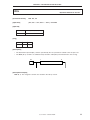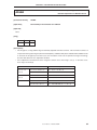
1
To our customers,
Old Company Name in Catalogs and Other Documents
On April 1st, 2010, NEC Electronics Corporation merged with Renesas Technology
Corporation, and Renesas Electronics Corporation took over all the business of both
companies. Therefore, although the old company name remains in this document, it is a valid
Renesas Electronics document. We appreciate your understanding.
Renesas Electronics website: http://www.renesas.com
April 1st, 2010
Renesas Electronics Corporation
Issued by: Renesas Electronics Corporation (http://www.renesas.com)
Send any inquiries to http://www.renesas.com/inquiry.
Notice
1.
2.
3.
4.
5.
6.
7.
All information included in this document is current as of the date this document is issued. Such information, however, is
subject to change without any prior notice. Before purchasing or using any Renesas Electronics products listed herein, please
confirm the latest product information with a Renesas Electronics sales office. Also, please pay regular and careful attention to
additional and different information to be disclosed by Renesas Electronics such as that disclosed through our website.
Renesas Electronics does not assume any liability for infringement of patents, copyrights, or other intellectual property rights
of third parties by or arising from the use of Renesas Electronics products or technical information described in this document.
No license, express, implied or otherwise, is granted hereby under any patents, copyrights or other intellectual property rights
of Renesas Electronics or others.
You should not alter, modify, copy, or otherwise misappropriate any Renesas Electronics product, whether in whole or in part.
Descriptions of circuits, software and other related information in this document are provided only to illustrate the operation of
semiconductor products and application examples. You are fully responsible for the incorporation of these circuits, software,
and information in the design of your equipment. Renesas Electronics assumes no responsibility for any losses incurred by
you or third parties arising from the use of these circuits, software, or information.
When exporting the products or technology described in this document, you should comply with the applicable export control
laws and regulations and follow the procedures required by such laws and regulations. You should not use Renesas
Electronics products or the technology described in this document for any purpose relating to military applications or use by
the military, including but not limited to the development of weapons of mass destruction. Renesas Electronics products and
technology may not be used for or incorporated into any products or systems whose manufacture, use, or sale is prohibited
under any applicable domestic or foreign laws or regulations.
Renesas Electronics has used reasonable care in preparing the information included in this document, but Renesas Electronics
does not warrant that such information is error free. Renesas Electronics assumes no liability whatsoever for any damages
incurred by you resulting from errors in or omissions from the information included herein.
Renesas Electronics products are classified according to the following three quality grades: “Standard”, “High Quality”, and
“Specific”. The recommended applications for each Renesas Electronics product depends on the product’s quality grade, as
indicated below. You must check the quality grade of each Renesas Electronics product before using it in a particular
application. You may not use any Renesas Electronics product for any application categorized as “Specific” without the prior
written consent of Renesas Electronics. Further, you may not use any Renesas Electronics product for any application for
which it is not intended without the prior written consent of Renesas Electronics. Renesas Electronics shall not be in any way
liable for any damages or losses incurred by you or third parties arising from the use of any Renesas Electronics product for an
application categorized as “Specific” or for which the product is not intended where you have failed to obtain the prior written
consent of Renesas Electronics. The quality grade of each Renesas Electronics product is “Standard” unless otherwise
expressly specified in a Renesas Electronics data sheets or data books, etc.
“Standard”:
8.
9.
10.
11.
12.
Computers; office equipment; communications equipment; test and measurement equipment; audio and visual
equipment; home electronic appliances; machine tools; personal electronic equipment; and industrial robots.
“High Quality”: Transportation equipment (automobiles, trains, ships, etc.); traffic control systems; anti-disaster systems; anticrime systems; safety equipment; and medical equipment not specifically designed for life support.
“Specific”:
Aircraft; aerospace equipment; submersible repeaters; nuclear reactor control systems; medical equipment or
systems for life support (e.g. artificial life support devices or systems), surgical implantations, or healthcare
intervention (e.g. excision, etc.), and any other applications or purposes that pose a direct threat to human life.
You should use the Renesas Electronics products described in this document within the range specified by Renesas Electronics,
especially with respect to the maximum rating, operating supply voltage range, movement power voltage range, heat radiation
characteristics, installation and other product characteristics. Renesas Electronics shall have no liability for malfunctions or
damages arising out of the use of Renesas Electronics products beyond such specified ranges.
Although Renesas Electronics endeavors to improve the quality and reliability of its products, semiconductor products have
specific characteristics such as the occurrence of failure at a certain rate and malfunctions under certain use conditions. Further,
Renesas Electronics products are not subject to radiation resistance design. Please be sure to implement safety measures to
guard them against the possibility of physical injury, and injury or damage caused by fire in the event of the failure of a
Renesas Electronics product, such as safety design for hardware and software including but not limited to redundancy, fire
control and malfunction prevention, appropriate treatment for aging degradation or any other appropriate measures. Because
the evaluation of microcomputer software alone is very difficult, please evaluate the safety of the final products or system
manufactured by you.
Please contact a Renesas Electronics sales office for details as to environmental matters such as the environmental
compatibility of each Renesas Electronics product. Please use Renesas Electronics products in compliance with all applicable
laws and regulations that regulate the inclusion or use of controlled substances, including without limitation, the EU RoHS
Directive. Renesas Electronics assumes no liability for damages or losses occurring as a result of your noncompliance with
applicable laws and regulations.
This document may not be reproduced or duplicated, in any form, in whole or in part, without prior written consent of Renesas
Electronics.
Please contact a Renesas Electronics sales office if you have any questions regarding the information contained in this
document or Renesas Electronics products, or if you have any other inquiries.
(Note 1) “Renesas Electronics” as used in this document means Renesas Electronics Corporation and also includes its majorityowned subsidiaries.
(Note 2) “Renesas Electronics product(s)” means any product developed or manufactured by or for Renesas Electronics.
User’s Manual
78K/0 Series
Instructions
Common to 78K/0 Series
Document No. U12326EJ4V0UM00 (4th edition)
Date Published October 2001 N CP(K)
©
Printed in Japan
1995
[MEMO]
2
User's Manual U12326EJ4V0UM
NOTES FOR CMOS DEVICES
1
PRECAUTION AGAINST ESD FOR SEMICONDUCTORS
Note:
Strong electric field, when exposed to a MOS device, can cause destruction of the gate oxide and
ultimately degrade the device operation. Steps must be taken to stop generation of static electricity
as much as possible, and quickly dissipate it once, when it has occurred. Environmental control
must be adequate. When it is dry, humidifier should be used. It is recommended to avoid using
insulators that easily build static electricity. Semiconductor devices must be stored and transported
in an anti-static container, static shielding bag or conductive material. All test and measurement
tools including work bench and floor should be grounded. The operator should be grounded using
wrist strap. Semiconductor devices must not be touched with bare hands. Similar precautions need
to be taken for PW boards with semiconductor devices on it.
2
HANDLING OF UNUSED INPUT PINS FOR CMOS
Note:
No connection for CMOS device inputs can be cause of malfunction. If no connection is provided
to the input pins, it is possible that an internal input level may be generated due to noise, etc., hence
causing malfunction. CMOS devices behave differently than Bipolar or NMOS devices. Input levels
of CMOS devices must be fixed high or low by using a pull-up or pull-down circuitry. Each unused
pin should be connected to V DD or GND with a resistor, if it is considered to have a possibility of
being an output pin. All handling related to the unused pins must be judged device by device and
related specifications governing the devices.
3
STATUS BEFORE INITIALIZATION OF MOS DEVICES
Note:
Power-on does not necessarily define initial status of MOS device. Production process of MOS
does not define the initial operation status of the device. Immediately after the power source is
turned ON, the devices with reset function have not yet been initialized. Hence, power-on does
not guarantee out-pin levels, I/O settings or contents of registers. Device is not initialized until the
reset signal is received. Reset operation must be executed immediately after power-on for devices
having reset function.
IEBus is a trademark of NEC Corporation.
Caution: Purchase of NEC I 2C components conveys a license under the Philips I2C Patent Rights to use these
components in an I 2C system, provided that the system conforms to the I2C Standard Specification as
defined by Philips.
User's Manual U12326EJ4V0UM
3
The export of these products from Japan is regulated by the Japanese government. The export of some or all of these
products may be prohibited without governmental license. To export or re-export some or all of these products from a
country other than Japan may also be prohibited without a license from that country. Please call an NEC sales
representative.
• The information in this document is current as of August, 2001. The information is subject to
change without notice. For actual design-in, refer to the latest publications of NEC's data sheets or
data books, etc., for the most up-to-date specifications of NEC semiconductor products. Not all
products and/or types are available in every country. Please check with an NEC sales representative
for availability and additional information.
• No part of this document may be copied or reproduced in any form or by any means without prior
written consent of NEC. NEC assumes no responsibility for any errors that may appear in this document.
• NEC does not assume any liability for infringement of patents, copyrights or other intellectual property rights of
third parties by or arising from the use of NEC semiconductor products listed in this document or any other
liability arising from the use of such products. No license, express, implied or otherwise, is granted under any
patents, copyrights or other intellectual property rights of NEC or others.
• Descriptions of circuits, software and other related information in this document are provided for illustrative
purposes in semiconductor product operation and application examples. The incorporation of these
circuits, software and information in the design of customer's equipment shall be done under the full
responsibility of customer. NEC assumes no responsibility for any losses incurred by customers or third
parties arising from the use of these circuits, software and information.
• While NEC endeavours to enhance the quality, reliability and safety of NEC semiconductor products, customers
agree and acknowledge that the possibility of defects thereof cannot be eliminated entirely. To minimize
risks of damage to property or injury (including death) to persons arising from defects in NEC
semiconductor products, customers must incorporate sufficient safety measures in their design, such as
redundancy, fire-containment, and anti-failure features.
• NEC semiconductor products are classified into the following three quality grades:
"Standard", "Special" and "Specific". The "Specific" quality grade applies only to semiconductor products
developed based on a customer-designated "quality assurance program" for a specific application. The
recommended applications of a semiconductor product depend on its quality grade, as indicated below.
Customers must check the quality grade of each semiconductor product before using it in a particular
application.
"Standard": Computers, office equipment, communications equipment, test and measurement equipment, audio
and visual equipment, home electronic appliances, machine tools, personal electronic equipment
and industrial robots
"Special": Transportation equipment (automobiles, trains, ships, etc.), traffic control systems, anti-disaster
systems, anti-crime systems, safety equipment and medical equipment (not specifically designed
for life support)
"Specific": Aircraft, aerospace equipment, submersible repeaters, nuclear reactor control systems, life
support systems and medical equipment for life support, etc.
The quality grade of NEC semiconductor products is "Standard" unless otherwise expressly specified in NEC's
data sheets or data books, etc. If customers wish to use NEC semiconductor products in applications not
intended by NEC, they must contact an NEC sales representative in advance to determine NEC's willingness
to support a given application.
(Note)
(1) "NEC" as used in this statement means NEC Corporation and also includes its majority-owned subsidiaries.
(2) "NEC semiconductor products" means any semiconductor product developed or manufactured by or for
NEC (as defined above).
M8E 00. 4
4
User's Manual U12326EJ4V0UM
Regional Information
Some information contained in this document may vary from country to country. Before using any NEC
product in your application, pIease contact the NEC office in your country to obtain a list of authorized
representatives and distributors. They will verify:
•
Device availability
•
Ordering information
•
Product release schedule
•
Availability of related technical literature
•
Development environment specifications (for example, specifications for third-party tools and
components, host computers, power plugs, AC supply voltages, and so forth)
•
Network requirements
In addition, trademarks, registered trademarks, export restrictions, and other legal issues may also vary
from country to country.
NEC Electronics Inc. (U.S.)
NEC Electronics (Germany) GmbH
NEC Electronics Hong Kong Ltd.
Santa Clara, California
Tel: 408-588-6000
800-366-9782
Fax: 408-588-6130
800-729-9288
Benelux Office
Eindhoven, The Netherlands
Tel: 040-2445845
Fax: 040-2444580
Hong Kong
Tel: 2886-9318
Fax: 2886-9022/9044
NEC Electronics Hong Kong Ltd.
Velizy-Villacoublay, France
Tel: 01-3067-5800
Fax: 01-3067-5899
Seoul Branch
Seoul, Korea
Tel: 02-528-0303
Fax: 02-528-4411
NEC Electronics (France) S.A.
NEC Electronics Singapore Pte. Ltd.
Madrid Office
Madrid, Spain
Tel: 091-504-2787
Fax: 091-504-2860
Novena Square, Singapore
Tel: 253-8311
Fax: 250-3583
NEC Electronics (France) S.A.
NEC Electronics (Germany) GmbH
Duesseldorf, Germany
Tel: 0211-65 03 02
Fax: 0211-65 03 490
NEC Electronics (UK) Ltd.
Milton Keynes, UK
Tel: 01908-691-133
Fax: 01908-670-290
NEC Electronics Taiwan Ltd.
NEC Electronics Italiana s.r.l.
NEC Electronics (Germany) GmbH
Milano, Italy
Tel: 02-66 75 41
Fax: 02-66 75 42 99
Scandinavia Office
Taeby, Sweden
Tel: 08-63 80 820
Fax: 08-63 80 388
Taipei, Taiwan
Tel: 02-2719-2377
Fax: 02-2719-5951
NEC do Brasil S.A.
Electron Devices Division
Guarulhos-SP, Brasil
Tel: 11-6462-6810
Fax: 11-6462-6829
J01.2
User's Manual U12326EJ4V0UM
5
Major Revisions in This Edition
Page
Throughout
Description
Deletion of all information except for information common to
the 78K/0 Series (for individual product information, refer to the
user’s manual of each product).
The mark
6
shows major revised points.
User's Manual U12326EJ4V0UM
INTRODUCTION
Target Readers
This manual is intended for users who wish to understand the functions of
78K/0 Series products and to design and develop its application systems and
programs.
Purpose
This manual is intended to give users an understanding of the various kinds of
instruction functions of 78K/0 Series products.
Organization
This manual is broadly divided into the following sections.
• CPU functions
• Instruction set
• Explanation of instructions
How to Read This Manual
It is assumed that readers of this manual have general knowledge in the fields of
electrical engineering, logic circuits, and microcontrollers.
• To check the details of the functions of an instruction whose mnemonic is known:
→ Refer to APPENDICES B and C.
• To check an instruction whose mnemonic is not known but whose general
function is known:
→ Find the mnemonic in CHAPTER 4 INSTRUCTION SET and then check the
detailed functions in CHAPTER 5 EXPLANATION OF INSTRUCTIONS.
• To learn about the various kinds of 78K/0 Series product instructions in general:
→ Read this manual in the order of CONTENTS.
• To learn about the hardware functions of 78K/0 Series products:
→ See the separate user’s manuals.
Conventions
Data significance:
Higher digits on the left and lower digits on the right
Note:
Footnote for item marked with Note in the text
Caution:
Information requiring particular attention
Remark:
Supplementary information
Numeral representation:
Binary ................. XXXX or XXXXB
Decimal .............. XXXX
Hexadecimal ...... XXXXH
User's Manual U12326EJ4V0UM
7
Related Documents
The related documents indicated in this publication may include preliminary versions. However, preliminary
versions are not marked as such.
• Documents Common to 78K/0 Series
Document Name
User’s Manual Instructions
Application Note
Note
Document No.
This manual
Basic I
U12704E
Basic II
U10121E
Basic III
U10182E
Note Some subseries may not be covered.
Caution The related documents listed above are subject to change without notice. Be sure to use the
latest version of each document for designing.
8
User's Manual U12326EJ4V0UM
CONTENTS
CHAPTER 1
1.1
1.2
1.3
1.4
1.5
1.6
1.7
1.8
1.9
MEMORY SPACE ............................................................................................................... 12
Memory Spaces ................................................................................................................12
Internal Program Memory (Internal ROM) Space .......................................................... 12
Vector Table Area ............................................................................................................. 12
CALLT Instruction Table Area ......................................................................................... 12
CALLF Instruction Entry Area ......................................................................................... 12
Internal Data Memory (Internal RAM) Space .................................................................. 12
Special Function Register (SFR) Area ............................................................................ 13
External Memory Space ................................................................................................... 13
IEBusTM Register Area ...................................................................................................... 13
CHAPTER 2 REGISTERS ........................................................................................................................14
2.1 Control Registers ............................................................................................................. 14
2.2
2.3
2.1.1
Program counter (PC) ......................................................................................................... 14
2.1.2
Program status word (PSW) ............................................................................................... 14
2.1.3
Stack pointer (SP) ................................................................................................................ 16
General-Purpose Registers ............................................................................................. 17
Special Function Registers (SFRs) ................................................................................. 19
CHAPTER 3 ADDRESSING ..................................................................................................................... 20
3.1 Instruction Address Addressing ..................................................................................... 20
3.2
3.1.1
Relative addressing ............................................................................................................. 20
3.1.2
Immediate addressing ......................................................................................................... 21
3.1.3
Table indirect addressing ................................................................................................... 22
3.1.4
Register addressing ............................................................................................................ 23
Operand Address Addressing ........................................................................................24
3.2.1
Implied addressing .............................................................................................................. 24
3.2.2
Register addressing ............................................................................................................ 25
3.2.3
Direct addressing ................................................................................................................ 26
3.2.4
Short direct addressing ...................................................................................................... 27
3.2.5
Special-function register (SFR) addressing ...................................................................... 28
3.2.6
Register indirect addressing .............................................................................................. 29
3.2.7
Based addressing ................................................................................................................ 30
3.2.8
Based indexed addressing ................................................................................................. 30
3.2.9
Stack addressing ................................................................................................................. 31
CHAPTER 4 INSTRUCTION SET ............................................................................................................32
4.1 Operation ..........................................................................................................................32
4.2
4.1.1
Operand identifiers and description methods .................................................................. 32
4.1.2
Description of “operation” column .................................................................................... 33
4.1.3
Description of “flag operation” column ............................................................................ 33
4.1.4
Description of number of clocks ........................................................................................ 34
4.1.5
Instructions listed by addressing type .............................................................................. 34
Instruction Codes ............................................................................................................. 38
4.2.1
Description of instruction code table ................................................................................ 38
4.2.2
Instruction code list ............................................................................................................. 39
User's Manual U12326EJ4V0UM
9
CHAPTER 5 EXPLANATION OF INSTRUCTIONS ................................................................................. 46
5.1 8-Bit Data Transfer Instructions ...................................................................................... 48
5.2 16-Bit Data Transfer Instructions .................................................................................... 51
5.3 8-Bit Operation Instructions ............................................................................................ 54
5.4 16-Bit Operation Instructions .......................................................................................... 63
5.5 Multiply/Divide Instructions ............................................................................................ 67
5.6 Increment/Decrement Instructions ................................................................................. 70
5.7 Rotate Instructions ...........................................................................................................75
5.8 BCD Adjust Instructions .................................................................................................. 82
5.9 Bit Manipulation Instructions .......................................................................................... 85
5.10 Call Return Instructions ................................................................................................... 93
5.11 Stack Manipulation Instructions ................................................................................... 101
5.12 Unconditional Branch Instruction ................................................................................ 105
5.13 Conditional Branch Instructions ................................................................................... 107
5.14 CPU Control Instructions ..............................................................................................116
APPENDIX A REVISION HISTORY .....................................................................................................123
APPENDIX B INSTRUCTION INDEX (MNEMONIC: BY FUNCTION) ............................................. 124
APPENDIX C INSTRUCTION INDEX (MNEMONIC: IN ALPHABETICAL ORDER) ...................... 126
10
User's Manual U12326EJ4V0UM
LIST OF FIGURES
Figure No.
Title
Page
2-1
Program Counter Configuration .............................................................................................................. 14
2-2
Program Status Word Configuration ....................................................................................................... 14
2-3
Stack Pointer Configuration .................................................................................................................... 16
2-4
Data to Be Saved to Stack Memory ....................................................................................................... 16
2-5
Data to Be Reset from Stack Memory .................................................................................................... 16
2-6
General-Purpose Register Configuration ............................................................................................... 18
LIST OF TABLES
Table No.
Title
Page
2-1
General-Purpose Register Absolute Address Correspondence Table ..................................................... 17
4-1
Operand Identifiers and Description Methods .......................................................................................... 32
User's Manual U12326EJ4V0UM
11
CHAPTER 1
MEMORY SPACE
1.1 Memory Spaces
The 78K/0 Series product program memory map varies depending on the internal memory capacity. For details
of memory-mapped address area, refer to the user’s manual of each product.
1.2 Internal Program Memory (Internal ROM) Space
Each 78K/0 Series product has internal ROM in the address space. Program and table data, etc. are stored
in the ROM. Normally, this memory space is addressed by the program counter (PC). For details of the internal
ROM space, refer to the user’s manual of each product.
1.3 Vector Table Area
The 64-byte area 0000H to 003FH is reserved as a vector table area. The program start addresses for branch
upon RESET input or interrupt request generation are stored in the vector table area. Of the 16-bit address, the
lower 8 bits are stored at even addresses and the higher 8 bits are stored at odd addresses. For the vector table
area, refer to the user’s manual of each product.
1.4 CALLT Instruction Table Area
The 64-byte area 0040H to 007FH can store the subroutine entry address of a 1-byte call instruction (CALLT).
1.5 CALLF Instruction Entry Area
The 2048-byte area 0800H to 0FFFH can perform a direct subroutine call with a 2-byte call instruction (CALLF).
1.6 Internal Data Memory (Internal RAM) Space
78K/0 Series products incorporate the following RAMs. For details of these RAMs, refer to the user’s manual
of each product.
(1) Internal high-speed RAM
Each 78K/0 Series product incorporates an internal high-speed RAM. In the 32-byte area FEE0H to FEFFH
of these areas, 4 banks of general-purpose registers, each bank consisting of eight 8-bit registers, are
allocated.
The internal high-speed RAM can also be used as a stack memory.
(2) Buffer RAM
There are some products in the 78K/0 Series to which buffer RAM is allocated. This RAM is used to store
the transfer/receive data of serial interface channel 1 (3-wire serial I/O mode with automatic transfer/receive
function). If not used in this mode, the buffer RAM can also be used as an ordinary RAM area.
12
User's Manual U12326EJ4V0UM
CHAPTER 1 MEMORY SPACE
(3) RAM for VFD display
There are some products in the 78K/0 Series to which RAM for VFD display is allocated. This RAM can
also be used as an ordinary RAM area.
(4) Internal expansion RAM
There are some products in the 78K/0 Series to which internal expansion RAM is allocated.
(5) RAM for LCD display
There are some products in the 78K/0 Series to which RAM for LCD display is allocated. This RAM can
also be used as an ordinary RAM area.
1.7 Special Function Register (SFR) Area
On-chip peripheral hardware special function registers (SFRs) are allocated in the area FF00H to FFFFH (for
details of the special function registers, refer to the user’s manual of each product).
Caution Do not access addresses to which SFRs are not allocated. If an address is erroneously
accessed, the CPU may become deadlocked.
1.8 External Memory Space
This is an external memory space that can be accessed by setting the memory extension mode register. This
space can store program and table data, and be assigned peripheral devices.
For details of the products in which an external memory space can be used, refer to the user’s manual of each
product.
1.9 IEBusTM Register Area
IEBus registers that are used to control the IEBus controller are allocated to the IEBus register area.
For details of the products that incorporate an IEBus controller, refer to the user’s manual of each product.
User's Manual U12326EJ4V0UM
13
CHAPTER 2 REGISTERS
2.1 Control Registers
The control registers control the program sequence, statuses and stack memory. A program counter, a program
status word and a stack pointer are the control registers.
2.1.1 Program counter (PC)
The program counter is a 16-bit register that holds the address information of the next program to be executed.
In normal operation, the PC is automatically incremented according to the number of bytes of the instruction
to be fetched. When a branch instruction is executed, immediate data and register contents are set.
RESET input sets the reset vector table values at addresses 0000H and 0001H to the program counter.
Figure 2-1. Program Counter Configuration
15
0
PC
2.1.2 Program status word (PSW)
The program status word is an 8-bit register consisting of various flags to be set/reset by instruction execution.
Program status word contents are automatically stacked upon interrupt request generation or PUSH PSW
instruction execution and are automatically reset upon execution of the RETB, RETI and POP PSW instructions.
RESET input sets the PSW to 02H.
Figure 2-2. Program Status Word Configuration
7
IE
14
0
Z
RBS1
AC
RBS0
0
User's Manual U12326EJ4V0UM
ISP
CY
CHAPTER 2 REGISTERS
(1) Interrupt enable flag (IE)
This flag controls the interrupt request acknowledgement operations of the CPU.
When IE = 0, the IE flag is set to interrupt disable (DI), and interrupts other than non-maskable interrupts
are all disabled.
When IE = 1, the IE flag is set to interrupt enable (EI), and interrupt request acknowledgement is controlled
by an in-service priority flag (ISP), an interrupt mask flag for various interrupt sources, and a priority
specification flag.
This flag is reset (0) upon DI instruction execution or interrupt request acknowledgment and is set (1) upon
execution of the EI instruction.
(2) Zero flag (Z)
When the operation result is zero, this flag is set (1). It is reset (0) in all other cases.
(3) Register bank select flags (RBS0 and RBS1)
These are 2-bit flags used to select one of the four register banks.
In these flags, the 2-bit information that indicates the register bank selected by SBL RBn instruction
execution is stored.
(4) Auxiliary carry flag (AC)
If the operation result has a carry from bit 3 or a borrow at bit 3, this flag is set (1). It is reset (0) in all other
cases.
(5) In-service priority flag (ISP)
This flag manages the priority of acknowledgeable maskable vectored interrupts. When ISP = 0, vectored
interrupt requests specified as low priority by the priority specification flag register (PR) are disabled for
acknowledgment. Actual acknowledgment for interrupt requests is controlled by the state of the interrupt
enable flag (IE).
(6) Carry flag (CY)
This flag stores an overflow or underflow upon add/subtract instruction execution. It stores the shift-out
value upon rotate instruction execution and functions as a bit accumulator during bit manipulation
instruction execution.
User's Manual U12326EJ4V0UM
15
CHAPTER 2 REGISTERS
2.1.3 Stack pointer (SP)
This is a 16-bit register that holds the start address of the memory stack area. Only the internal high-speed
RAM area can be set as the stack area.
Figure 2-3. Stack Pointer Configuration
15
0
SP
The SP is decremented ahead of write (save) to the stack memory and is incremented after read (reset) from
the stack memory.
Each stack operation saves/resets data as shown in Figures 2-4 and 2-5.
Caution Since RESET input makes SP contents undefined, be sure to initialize the SP before instruction
execution.
Figure 2-4. Data to Be Saved to Stack Memory
PUSH rp
instruction
Interrupt and
BRK instructions
CALL, CALLF and
CALLT instructions
SP
SP
SP _ 2
SP
SP _ 2
SP _ 3
SP _ 3
PC7-PC0
SP _ 2
Lower half
register pairs
SP _ 2
PC7-PC0
SP _ 2
PC15-PC8
SP _ 1
Upper half
register pairs
SP _ 1
PC15-PC8
SP _ 1
PSW
SP
SP
SP
Figure 2-5. Data to Be Reset from Stack Memory
POP rp
instruction
SP
RET instruction
RETI and RETB
instructions
SP
Lower half
register pairs
SP
PC7-PC0
SP
PC7-PC0
SP + 1
Upper half
register pairs
SP + 1
PC15-PC8
SP + 1
PC15-PC8
SP + 2
PSW
SP + 2
SP
SP + 2
SP
16
User's Manual U12326EJ4V0UM
SP + 3
CHAPTER 2 REGISTERS
2.2 General-Purpose Registers
General-purpose registers are mapped at particular addresses (FEE0H to FEFFH) of the data memory. These
registers consist of 4 banks, each bank consisting of eight 8-bit registers (X, A, C, B, E, D, L and H).
In addition that each register can be used as an 8-bit register, two 8-bit registers in pairs can be used as a 16bit register (AX, BC, DE and HL).
General-purpose registers can be described in terms of functional names (X, A, C, B, E, D, L, H, AX, BC, DE
and HL) and absolute names (R0 to R7 and RP0 to RP3).
Register banks to be used for instruction execution are set with the CPU control instruction (SEL RBn). Because
of the 4-register bank configuration, an efficient program can be created by switching between a register for normal
processing and a register for processing upon interrupt generation for each bank.
Table 2-1. General-Purpose Register Absolute Address Correspondence Table
Bank Name
BANK0
BANK1
Register
Absolute Address
Bank Name
Register
Absolute Address
Functional
Absolute
Functional
Absolute
Name
Name
Name
Name
H
R7
FEFFH
H
R7
FEEFH
L
R6
FEFEH
L
R6
FEEEH
D
R5
FEFDH
D
R5
FEEDH
E
R4
FEFCH
E
R4
FEECH
B
R3
FEFBH
B
R3
FEEBH
C
R2
FEFAH
C
R2
FEEAH
A
R1
FEF9H
A
R1
FEE9H
X
R0
FEF8H
X
R0
FEE8H
H
R7
FEF7H
H
R7
FEE7H
L
R6
FEF6H
L
R6
FEE6H
D
R5
FEF5H
D
R5
FEE5H
E
R4
FEF4H
E
R4
FEE4H
B
R3
FEF3H
B
R3
FEE3H
C
R2
FEF2H
C
R2
FEE2H
A
R1
FEF1H
A
R1
FEE1H
X
R0
FEF0H
X
R0
FEE0H
BANK2
BANK3
User's Manual U12326EJ4V0UM
17
CHAPTER 2 REGISTERS
Figure 2-6. General-Purpose Register Configuration
(a) Absolute names
16-bit processing
8-bit processing
FEFFH
R7
BANK0
RP3
R6
FEF8H
FEF7H
R5
BANK1
RP2
R4
FEF0H
FEEFH
R3
BANK2
RP1
R2
FEE8H
FEE7H
R1
BANK3
RP0
R0
FEE0H
15
0
7
0
(b) Functional names
16-bit processing
8-bit processing
FEFFH
H
BANK0
HL
L
FEF8H
FEF7H
D
BANK1
DE
E
FEF0H
FEEFH
B
BANK2
BC
C
FEE8H
FEE7H
A
BANK3
AX
X
FEE0H
15
18
User's Manual U12326EJ4V0UM
0
7
0
CHAPTER 2 REGISTERS
2.3 Special Function Registers (SFRs)
Unlike a general-purpose register, each special-function register has a special function.
Special function registers are allocated in the 256-byte area FF00H to FFFFH.
Special function registers can be manipulated, like general-purpose registers, by operation, transfer and bit
manipulation instructions. The manipulatable bit units (1, 8, and 16) differ depending on the special function
register type.
Each manipulation bit unit can be specified as follows.
• 1-bit manipulation
Describes a symbol reserved by the assembler for the 1-bit manipulation instruction operand (sfr.bit). This
manipulation can also be specified by an address.
• 8-bit manipulation
Describes a symbol reserved by the assembler for the 8-bit manipulation instruction operand (sfr). This
manipulation can also be specified by an address.
• 16-bit manipulation
Describes a symbol reserved by the assembler for the 16-bit manipulation instruction operand (sfrp). When
addressing an address, describe an even address.
For details of the special function registers, refer to the user’s manual of each product.
Caution Do not access addresses to which SFRs are not allocated. If an address is erroneously
accessed, the CPU may become deadlocked.
User's Manual U12326EJ4V0UM
19
CHAPTER 3 ADDRESSING
3.1 Instruction Address Addressing
An instruction address is determined by program counter (PC) contents. The PC contents are normally
incremented (+1 for each byte) automatically according to the number of bytes of an instruction to be fetched each
time another instruction is executed. When a branch instruction is executed, the branch destination information
is set to the PC and branched by the following addressing (for details of each instruction, refer to CHAPTER 5
EXPLANATION OF INSTRUCTIONS).
3.1.1 Relative addressing
[Function]
The value obtained by adding 8-bit immediate data (displacement value: jdisp8) of an instruction code to
the start address of the following instruction is transferred to the program counter (PC) and branched. The
displacement value is treated as signed two’s complement data (–128 to +127) and bit 7 becomes a sign
bit. In other words, in relative addressing, the value is relatively transferred to the range between –128 and
+127 from the start address of the following instruction.
This function is carried out when the “BR $addr16” instruction or a conditional branch instruction is executed.
[Illustration]
15
0
... PC is the start address of
PC
the next instruction of
a BR instruction.
+
8
15
α
7
6
0
S
jdisp8
15
0
PC
When S = 0, α indicates all bits "0".
When S = 1, α indicates all bits "1".
20
User's Manual U12326EJ4V0UM
CHAPTER 3 ADDRESSING
3.1.2 Immediate addressing
[Function]
Immediate data in the instruction word is transferred to the program counter (PC) and branched.
This function is carried out when the “CALL !addr16” or “BR !addr16” or “CALLF !addr11” instruction is
executed. The CALL !addr16 and BR !addr16 instructions can be branched to all memory spaces. The
CALLF !addr11 instruction is branched to the area of 0800H to 0FFFH.
[Illustration]
CALL !addr16, BR !addr16 instruction
7
0
CALL or BR
Low Addr.
High Addr.
15
8 7
0
PC
CALLF !addr11 instruction
7 6
4
3
0
fa10 to fa8
CALLF
fa7 to fa0
15
PC
0
11 10
0
0
0
8 7
0
1
User's Manual U12326EJ4V0UM
21
CHAPTER 3 ADDRESSING
3.1.3 Table indirect addressing
[Function]
Table contents (branch destination address) of the particular location to be addressed by the lower-5-bit
immediate data of an instruction code from bit 1 to bit 5 are transferred to the program counter (PC) and
branched.
When the “CALLT [addr5]” instruction is executed, table indirect addressing is performed. Executing this
instruction enables the value to be branched to all memory spaces referencing the address stored in the
memory table of 40H to 7FH.
[Illustration]
7
Instruction code
6
1
5
1
1
ta4–0
1
15
Effective address
0
7
0
0
0
0
0
0
Memory (Table)
0
8
7
6
0
0
1
5
1 0
0
0
Low addr.
High addr.
Effective address+1
15
8
7
PC
22
User's Manual U12326EJ4V0UM
0
CHAPTER 3 ADDRESSING
3.1.4 Register addressing
[Function]
The register pair (AX) contents to be specified by an instruction word are transferred to the program counter
(PC) and branched.
This function is carried out when the “BR AX” instruction is executed.
[Illustration]
7
rp
0
7
A
15
0
X
8
7
0
PC
User's Manual U12326EJ4V0UM
23
CHAPTER 3 ADDRESSING
3.2 Operand Address Addressing
The following methods are available to specify the register and memory (addressing) to undergo manipulation
during instruction execution.
3.2.1 Implied addressing
[Function]
This addressing automatically specifies the address of the registers that function as an accumulator (A and
AX) in the general-purpose register area.
Of the 78K/0 Series instruction words, the following instructions employ implied addressing.
Instruction
Register to Be Specified by Implied Addressing
MULU
A register for multiplicand and AX register for product storage
DIVUW
AX register for dividend and quotient storage
ADJBA/ADJBS
A register for storage of numeric values targeted for decimal correction
ROR4/ROL4
A register for storage of digit data that undergoes digit rotation
[Operand format]
Because implied addressing can be automatically employed with an instruction, no particular operand format
is necessary.
[Description example]
In the case of MULU X
With an 8-bit x 8-bit multiply instruction, the product of the A register and X register is stored in AX. In this
example, the A and AX registers are specified by implied addressing.
24
User's Manual U12326EJ4V0UM
CHAPTER 3 ADDRESSING
3.2.2 Register addressing
[Function]
Register addressing accesses a general-purpose register as an operand. The general-purpose register to
be accessed is specified by the register bank selection flags (RBS0 and RBS1) and the register specification
codes (Rn and RPn) in the instruction codes.
Register addressing is carried out when an instruction with the following operand format is executed. When
an 8-bit register is specified, one of the eight registers is specified by 3 bits in the instruction code.
[Operand format]
Identifier
r
rp
Description
X, A, C, B, E, D, L, H
AX, BC, DE, HL
‘r’ and ‘rp’ can be described with absolute names (R0 to R7 and RP0 to RP3) as well as function names
(X, A, C, B, E, D, L, H, AX, BC, DE and HL).
[Description example]
MOV A, C; When selecting the C register for r
Instruction code
0
1
1
0
0
0
1
0
Register specification code
INCW DE; When selecting the DE register pair for rp
Instruction code
1
0
0
0
0
1
0
0
Register specification code
User's Manual U12326EJ4V0UM
25
CHAPTER 3 ADDRESSING
3.2.3 Direct addressing
[Function]
Direct addressing directly addresses the memory indicated by the immediate data in the instruction word.
[Operand format]
Identifier
addr16
Description
Label or 16-bit immediate data
[Description example]
MOV A, !FE00H; When setting !addr16 to FE00H
Instruction code
1
0
0
0
1
1
1
0
OP code
0
0
0
0
0
0
0
0
00H
1
1
1
1
1
1
1
0
FEH
[Illustration]
7
0
OP code
addr16 (lower)
addr16 (upper)
Memory
26
User's Manual U12326EJ4V0UM
CHAPTER 3 ADDRESSING
3.2.4 Short direct addressing
[Function]
The memory to be manipulated in the fixed space is directly addressed with 8-bit data in an instruction word.
This addressing is applied to the 256-byte fixed space FE20H to FF1FH. An internal high-speed RAM and
special function registers (SFRs) are mapped at FE20H to FEFFH and FF00H to FF1FH, respectively.
The SFR area (FF00H to FF1FH) where short direct addressing is applied is a part of the entire SFR area.
Ports that are frequently accessed in a program, a compare register of the timer/event counter and a capture
register of the timer/event counter are mapped in the area FF00H through FF1FH, and these SFRs can be
manipulated with a small number of bytes and clocks.
When 8-bit immediate data is at 20H to FFH, bit 8 of an effective address is set to 0. When it is at 00H to
1FH, bit 8 is set to 1. See [Illustration] below.
[Operand format]
Identifier
saddr
Description
Label or FE20H to FF1FH immediate data
saddrp
Label or FE20H to FF1FH immediate data (even address only)
[Description example]
MOV FE30H, #50H; When setting saddr to FE30H and the immediate data to 50H
Instruction code
0
0
0
1
0
0
0
1
OP code
0
0
1
1
0
0
0
0
30H (saddr-offset)
0
1
0
1
0
0
0
0
50H (immediate data)
[Illustration]
7
0
OP code
saddr-offset
Short direct memory
15
Effective
address
1
8 7
1
1
1
1
1
1
0
α
When 8-bit immediate data is 20H to FFH, α = 0.
When 8-bit immediate data is 00H to 1FH, α = 1.
User's Manual U12326EJ4V0UM
27
CHAPTER 3 ADDRESSING
3.2.5 Special-function register (SFR) addressing
[Function]
A memory-mapped special function register (SFR) is addressed with 8-bit immediate data in an instruction
word.
This addressing is applied to the 240-byte spaces FF00H to FFCFH and FFE0H to FFFFH. However, the
SFRs mapped at FF00H to FF1FH can be accessed with short direct addressing.
[Operand format]
Identifier
Description
sfr
Special function register name
sfrp
16-bit-manipulatable special function register name (even address only)
[Description example]
MOV PM0, A; When selecting PM0 for sfr
Instruction code
1
1
1
1
0
1
1
0
OP code
0
0
1
0
0
0
0
0
20H (sfr-offset)
[Illustration]
7
0
OP code
sfr-offset
SFR
15
Effective
address
28
1
8 7
1
1
1
1
1
1
0
1
User's Manual U12326EJ4V0UM
CHAPTER 3 ADDRESSING
3.2.6 Register indirect addressing
[Function]
Register indirect addressing addresses memory with register pair contents specified as an operand. The
register pair to be accessed is specified by the register bank selection flags (RBS0 and RBS1) and the
register pair specification in instruction codes.
[Operand format]
Identifier
Description
—
[DE], [HL]
[Description example]
MOV A, [DE]; When selecting register pair [DE]
Instruction code
1
0
0
0
0
1
0
1
[Illustration]
15
DE
8 7
0
E
D
7
Memory
0
Memory address specified
by register pair DE
Contents of memory to be
addressed are transferred
7
0
A
User's Manual U12326EJ4V0UM
29
CHAPTER 3 ADDRESSING
3.2.7 Based addressing
[Function]
8-bit immediate data is added to the contents of the HL register pair as a base register and the sum is used
to address the memory. The HL register pair to be accessed is in the register bank specified by the register
bank select flag (RBS0 and RBS1). Addition is performed by expanding the offset data as a positive number
to 16 bits. A carry from the 16th bit is ignored. This addressing can be carried out for all the memory spaces.
[Operand format]
Identifier
—
Description
[HL+byte]
[Description example]
MOV A, [HL+10H]; When setting byte to 10H
Instruction code
1
0
1
0
1
1
1
0
0
0
0
1
0
0
0
0
3.2.8 Based indexed addressing
[Function]
The B or C register contents specified in an instruction word are added to the contents of the HL register
pair as a base register and the sum is used to address the memory. The HL, B, and C registers to be accessed
are registers in the register bank specified by the register bank select flag (RBS0 to RBS1). Addition is
performed by expanding the B or C register as a positive number to 16 bits. A carry from the 16th bit is
ignored. This addressing can be carried out for all the memory spaces.
[Operand format]
Identifier
—
Description
[HL+B], [HL+C]
[Description example]
In the case of MOV A, [HL+B]
Instruction code
30
1
0
1
0
User's Manual U12326EJ4V0UM
1
0
1
1
CHAPTER 3 ADDRESSING
3.2.9 Stack addressing
[Function]
The stack area is indirectly addressed with the stack pointer (SP) contents.
This addressing method is automatically employed when the PUSH, POP, subroutine call and RETURN
instructions are executed or the register is saved/reset upon generation of an interrupt request.
Stack addressing enables addressing of the internal high-speed RAM area only.
[Description example]
In the case of PUSH DE
Instruction code
1
0
1
1
User's Manual U12326EJ4V0UM
0
1
0
1
31
CHAPTER 4
INSTRUCTION SET
This chapter lists the instructions in the 78K/0 Series instruction set. The instructions are common to all
78K/0 Series products.
4.1 Operation
For the operation list for each product, refer to the user’s manual of each product.
4.1.1 Operand identifiers and description methods
Operands are described in the “Operand” column of each instruction in accordance with the description method
of the instruction operand identifier (refer to the assembler specifications for details). When there are two or more
description methods, select one of them. Alphabetic letters in capitals and the symbols, #, !, $ and [ ] are key
words and are described as they are. Each symbol has the following meaning.
• #: Immediate data specification
• !:
Absolute address specification
• $: Relative address specification
• [ ]: Indirect address specification
In the case of immediate data, describe an appropriate numeric value or a label. When using a label, be sure
to describe the #, !, $ and [ ] symbols.
For operand register identifiers, r and rp, either function names (X, A, C, etc.) or absolute names (names in
parentheses in the table below, R0, R1, R2, etc.) can be used for description.
Table 4-1. Operand Identifiers and Description Methods
Identifier
Description Method
r
rp
sfr
sfrp
X (R0), A (R1), C (R2), B (R3), E (R4), D (R5), L (R6), H (R7)
AX (RP0), BC (RP1), DE (RP2), HL (RP3)
Special-function register symbolNote
Special-function register symbols (16-bit manipulatable register even addresses only)Note
saddr
saddrp
FE20H to FF1FH Immediate data or labels
FE20H to FF1FH Immediate data or labels (even addresses only)
addr16
addr11
addr5
0000H to FFFFH Immediate data or labels (Only even addresses for 16-bit data transfer instructions)
0800H to 0FFFH Immediate data or labels
0040H to 007FH Immediate data or labels (even addresses only)
word
byte
bit
16-bit immediate data or label
8-bit immediate data or label
3-bit immediate data or label
RBn
RB0 to RB3
Note FFD0H to FFDFH are not addressable.
Remark Refer to the user’s manual of each product for the symbols of special function registers.
32
User's Manual U12326EJ4V0UM
CHAPTER 4 INSTRUCTION SET
4.1.2 Description of “operation” column
A:
A register; 8-bit accumulator
X:
X register
B:
B register
C:
C register
D:
D register
E:
E register
H:
H register
L:
L register
AX:
AX register pair; 16-bit accumulator
BC:
BC register pair
DE:
DE register pair
HL:
HL register pair
PC:
Program counter
SP:
Stack pointer
PSW:
Program status word
CY:
Carry flag
AC:
Auxiliary carry flag
Z:
Zero flag
RBS:
Register bank select flag
IE:
Interrupt request enable flag
NMIS:
Flag indicating non-maskable interrupt servicing in progress
( ):
Memory contents indicated by address or register contents in parentheses
XH, XL: Higher 8 bits and lower 8 bits of 16-bit register
V
Logical product (AND)
V:
Logical sum (OR)
V:
—:
Exclusive logical sum (exclusive OR)
:
Inverted data
addr16: 16-bit immediate data or label
jdisp8: Signed 8-bit data (displacement value)
4.1.3 Description of “flag operation” column
(Blank): Unchanged
0:
Cleared to 0
1:
Set to 1
×:
Set/cleared according to the result
R:
Previously saved value is restored
User's Manual U12326EJ4V0UM
33
CHAPTER 4 INSTRUCTION SET
4.1.4 Description of number of clocks
1 instruction clock cycle is 1 CPU clock cycle (fCPU) selected by the processor clock control register (PCC).
4.1.5 Instructions listed by addressing type
(1) 8-bit instructions
MOV, XCH, ADD, ADDC, SUB, SUBC, AND, OR, XOR, CMP, MULU, DIVUW, INC, DEC, ROR, ROL,
RORC, ROLC, ROR4, ROL4, PUSH, POP, DBNZ
34
User's Manual U12326EJ4V0UM
CHAPTER 4 INSTRUCTION SET
2nd Operand
#byte
A
rNote
sfr
saddr
!addr16
PSW
[DE]
[HL]
r
1
None
[HL+B]
[HL+C]
1st Operand
A
[HL+byte] $addr16
ADD
MOV
MOV
MOV
MOV
ADDC
SUB
XCH
ADD
XCH
XCH
ADD
XCH
ADD
SUBC
AND
ADDC
SUB
ADDC
SUB
OR
XOR
SUBC
AND
CMP
MOV
MOV
MOV
MOV
MOV
ROR
XCH
XCH
ADD
XCH
ADD
ROL
RORC
ADDC
SUB
ADDC
SUB
ADDC
SUB
ROLC
SUBC
AND
SUBC
AND
SUBC
AND
SUBC
AND
OR
XOR
OR
XOR
OR
XOR
OR
XOR
OR
XOR
CMP
CMP
CMP
CMP
CMP
MOV
ADD
INC
DEC
ADDC
SUB
SUBC
AND
OR
XOR
CMP
B, C
DBNZ
sfr
MOV
MOV
saddr
MOV
ADD
MOV
DBNZ
INC
DEC
ADDC
SUB
SUBC
AND
OR
XOR
CMP
!addr16
MOV
PSW
MOV
MOV
[DE]
MOV
[HL]
MOV
PUSH
POP
ROR4
ROL4
[HL+byte]
[HL+B]
MOV
[HL+C]
X
MULU
C
DIVUW
Note
Except r = A.
User's Manual U12326EJ4V0UM
35
CHAPTER 4 INSTRUCTION SET
(2) 16-bit instructions
MOVW, XCHW, ADDW, SUBW, CMPW, PUSH, POP, INCW, DECW
2nd Operand
#word
AX
rpNote
sfrp
saddrp
!addr16
SP
None
1st Operand
AX
ADDW
SUBW
MOVW
XCHW
MOVW
MOVW
MOVW
MOVW
CMPW
rp
MOVW
MOVWNote
INCW
DECW
PUSH
POP
sfrp
MOVW
MOVW
saddrp
MOVW
MOVW
!addr16
MOVW
SP
Note
MOVW
MOVW
Only when rp = BC, DE or HL.
(3) Bit manipulation instructions
MOV1, AND1, OR1, XOR1, SET1, CLR1, NOT1, BT, BF, BTCLR
2nd Operand
A.bit
sfr.bit
saddr.bit
PSW.bit
[HL].bit
CY
$addr16
None
1st Operand
A.bit
MOV1
BT
BF
SET1
CLR1
BTCLR
sfr.bit
MOV1
BT
BF
SET1
CLR1
BTCLR
saddr.bit
MOV1
BT
BF
SET1
CLR1
BTCLR
PSW.bit
MOV1
BT
BF
SET1
CLR1`
BTCLR
[HL].bit
MOV1
BT
BF
SET1
CLR1
BTCLR
CY
36
MOV1
AND1
MOV1
AND1
MOV1
AND1
MOV1
AND1
MOV1
AND1
SET1
CLR1
OR1
XOR1
OR1
XOR1
OR1
XOR1
OR1
XOR1
OR1
XOR1
NOT1
User's Manual U12326EJ4V0UM
CHAPTER 4 INSTRUCTION SET
(4) Call instructions/branch instructions
CALL, CALLF, CALLT, BR, BC, BNC, BZ, BNZ, BT, BF, BTCLR, DBNZ
2nd Operand
AX
!addr16
!addr11
[addr5]
$addr16
1st Operand
Basic Instructions
BR
CALL
CALLF
CALLT
BR
BR
BC
BNC
BZ
BNZ
Compound Instructions
BT
BF
BTCLR
DBNZ
(5) Other instructions
ADJBA, ADJBS, BRK, RET, RETI, RETB, SEL, NOP, EI, DI, HALT, STOP
User's Manual U12326EJ4V0UM
37
CHAPTER 4 INSTRUCTION SET
4.2 Instruction Codes
4.2.1 Description of instruction code table
r
rp
R2
R1
R0
reg
0
0
0
R0
0
0
1
0
1
0
RB
P1
P0
reg-pair
RB1
RB0
reg-bank
X
0
0
RP0
AX
0
0
RB0
R1
A
0
1
RP1
BC
0
1
RB1
0
R2
C
1
0
RP2
DE
1
0
RB2
1
1
R3
B
1
1
RP3
HL
1
1
RB3
1
0
0
R4
E
1
0
1
R5
D
1
1
0
R6
L
1
1
1
R7
H
Bn:
Immediate data corresponding to bit
Data:
8-bit immediate data corresponding to byte
Low/High byte: 16-bit immediate data corresponding to word
Saddr-offset:
16-bit address lower 8-bit offset data corresponding to saddr
Sfr-offset:
sfr 16-bit address lower 8-bit offset data
Low/High addr: 16-bit immediate data corresponding to addr16
jdisp:
Signed two’s complement data (8 bits) of relative address distance between the start
fa 10 to fa 0:
11 bits of immediate data corresponding to addr11
ta 4 to ta 0:
5 bits of immediate data corresponding to addr5
and branch addresses of the next instruction
38
User's Manual U12326EJ4V0UM
CHAPTER 4 INSTRUCTION SET
4.2.2 Instruction code list
Instruction
Mnemonic
Operands
Operation Code
Group
8-Bit Data
MOV
Transfer
B1
B2
r,#byte
1 0 1 0 0 R2 R1 R0
Data
saddr,#byte
0 0 0 1 0 0 0 1
Saddr-offset
Data
0 0 0 1 0 0 1 1
Sfr-offset
Data
sfr,#byte
XCH
A,r
Note
0 1 1 0 0 R2 R1 R0
r,A
Note
0 1 1 1 0 R2 R1 R0
B3
A,saddr
1 1 1 1 0 0 0 0
Saddr-offset
saddr,A
1 1 1 1 0 0 1 0
Saddr-offset
A,sfr
1 1 1 1 0 1 0 0
Sfr-offset
sfr,A
1 1 1 1 0 1 1 0
Sfr-offset
A,!addr16
1 0 0 0 1 1 1 0
Low addr
High addr
!addr16,A
1 0 0 1 1 1 1 0
Low addr
High addr
PSW,#byte
0 0 0 1 0 0 0 1 0 0 0 1 1 1 1 0
A,PSW
1 1 1 1 0 0 0 0 0 0 0 1 1 1 1 0
PSW,A
1 1 1 1 0 0 1 0 0 0 0 1 1 1 1 0
A,[DE]
1 0 0 0 0 1 0 1
[DE],A
1 0 0 1 0 1 0 1
A,[HL]
1 0 0 0 0 1 1 1
[HL],A
1 0 0 1 0 1 1 1
A,[HL+byte]
1 0 1 0 1 1 1 0
Data
[HL+byte],A
1 0 1 1 1 1 1 0
Data
A,[HL+B]
1 0 1 0 1 0 1 1
[HL+B],A
1 0 1 1 1 0 1 1
A,[HL+C]
1 0 1 0 1 0 1 0
[HL+C],A
1 0 1 1 1 0 1 0
A,r
Note
B4
Data
0 0 1 1 0 R2 R1 R0
A,saddr
1 0 0 0 0 0 1 1
Saddr-offset
A,sfr
1 0 0 1 0 0 1 1
Sfr-offset
A,!addr16
1 1 0 0 1 1 1 0
Low addr
A,[DE]
0 0 0 0 0 1 0 1
A,[HL]
0 0 0 0 0 1 1 1
A,[HL+byte]
1 1 0 1 1 1 1 0
A,[HL+B]
0 0 1 1 0 0 0 1 1 0 0 0 1 0 1 1
A,[HL+C]
0 0 1 1 0 0 0 1 1 0 0 0 1 0 1 0
High addr
Data
Note Except r = A.
User's Manual U12326EJ4V0UM
39
CHAPTER 4 INSTRUCTION SET
Instruction
Mnemonic
Operands
Operation Code
Group
B1
B2
B3
B4
16-Bit Data MOVW
rp,#word
0 0 0 1 0 P1 P0 0
Low byte
High byte
Transfer
saddrp,#word
1 1 1 0 1 1 1 0
Saddr-offset
Low byte
High byte
sfrp,#word
1 1 1 1 1 1 1 0
Sfr-offset
Low byte
High byte
AX,saddrp
1 0 0 0 1 0 0 1
Saddr-offset
saddrp,AX
1 0 0 1 1 0 0 1
Saddr-offset
AX,sfrp
1 0 1 0 1 0 0 1
Sfr-offset
sfrp,AX
1 0 1 1 1 0 0 1
Sfr-offset
8-Bit
AX,rp
Note 1
1 1 0 0 0 P1 P0 0
rp,AX
Note 1
1 1 0 1 0 P1 P0 0
AX,!addr16
0 0 0 0 0 0 1 0
Low addr
High addr
!addr16,AX
0 0 0 0 0 0 1 1
Low addr
High addr
Note 1
XCHW
AX,rp
ADD
A,#byte
0 0 0 0 1 1 0 1
Data
saddr,#byte
1 0 0 0 1 0 0 0
Saddr-offset
Operation
A,r
ADDC
Note 2
1 1 1 0 0 P1 P0 0
0 1 1 0 0 0 0 1 0 0 0 0 1 R2 R1 R0
r,A
0 1 1 0 0 0 0 1 0 0 0 0 0 R2 R1 R0
A,saddr
0 0 0 0 1 1 1 0
Saddr-offset
A,!addr16
0 0 0 0 1 0 0 0
Low addr
A,[HL]
0 0 0 0 1 1 1 1
A,[HL+byte]
0 0 0 0 1 0 0 1
A,[HL+B]
0 0 1 1 0 0 0 1 0 0 0 0 1 0 1 1
A,[HL+C]
0 0 1 1 0 0 0 1 0 0 0 0 1 0 1 0
A,#byte
0 0 1 0 1 1 0 1
Data
1 0 1 0 1 0 0 0
Saddr-offset
saddr,#byte
A,r
Note 2
High addr
Data
Data
0 1 1 0 0 0 0 1 0 0 1 0 1 R2 R1 R0
r,A
0 1 1 0 0 0 0 1 0 0 1 0 0 R2 R1 R0
A,saddr
0 0 1 0 1 1 1 0
Saddr-offset
A,!addr16
0 0 1 0 1 0 0 0
Low addr
A,[HL]
0 0 1 0 1 1 1 1
A,[HL+byte]
0 0 1 0 1 0 0 1
A,[HL+B]
0 0 1 1 0 0 0 1 0 0 1 0 1 0 1 1
A,[HL+C]
0 0 1 1 0 0 0 1 0 0 1 0 1 0 1 0
Data
Notes 1. Only when rp = BC, DE or HL.
2. Except r = A.
40
Data
User's Manual U12326EJ4V0UM
High addr
CHAPTER 4 INSTRUCTION SET
Instruction
Mnemonic
Operands
Operation Code
Group
8-Bit
SUB
Operation
B1
B2
A,#byte
0 0 0 1 1 1 0 1
Data
saddr,#byte
1 0 0 1 1 0 0 0
Saddr-offset
A,r
SUBC
Note
0 1 1 0 0 0 0 1 0 0 0 1 0 R2 R1 R0
A,saddr
0 0 0 1 1 1 1 0
Saddr-offset
A,!addr16
0 0 0 1 1 0 0 0
Low addr
A,[HL]
0 0 0 1 1 1 1 1
A,[HL+byte]
0 0 0 1 1 0 0 1
A,[HL+B]
0 0 1 1 0 0 0 1 0 0 0 1 1 0 1 1
A,[HL+C]
0 0 1 1 0 0 0 1 0 0 0 1 1 0 1 0
A,#byte
0 0 1 1 1 1 0 1
Data
1 0 1 1 1 0 0 0
Saddr-offset
A,r
AND
Note
High addr
Data
0 1 1 0 0 0 0 1 0 0 1 1 1 R2 R1 R0
0 1 1 0 0 0 0 1 0 0 1 1 0 R2 R1 R0
A,saddr
0 0 1 1 1 1 1 0
Saddr-offset
A,!addr16
0 0 1 1 1 0 0 0
Low addr
A,[HL]
0 0 1 1 1 1 1 1
A,[HL+byte]
0 0 1 1 1 0 0 1
A,[HL+B]
0 0 1 1 0 0 0 1 0 0 1 1 1 0 1 1
A,[HL+C]
0 0 1 1 0 0 0 1 0 0 1 1 1 0 1 0
A,#byte
0 1 0 1 1 1 0 1
Data
saddr,#byte
1 1 0 1 1 0 0 0
Saddr-offset
Note
Data
Data
r,A
A,r
B4
0 1 1 0 0 0 0 1 0 0 0 1 1 R2 R1 R0
r,A
saddr,#byte
B3
High addr
Data
Data
0 1 1 0 0 0 0 1 0 1 0 1 1 R2 R1 R0
r,A
0 1 1 0 0 0 0 1 0 1 0 1 0 R2 R1 R0
A,saddr
0 1 0 1 1 1 1 0
Saddr-offset
A,!addr16
0 1 0 1 1 0 0 0
Low addr
A,[HL]
0 1 0 1 1 1 1 1
A,[HL+byte]
0 1 0 1 1 0 0 1
A,[HL+B]
0 0 1 1 0 0 0 1 0 1 0 1 1 0 1 1
A,[HL+C]
0 0 1 1 0 0 0 1 0 1 0 1 1 0 1 0
High addr
Data
Note Except r = A.
User's Manual U12326EJ4V0UM
41
CHAPTER 4 INSTRUCTION SET
Instruction
Mnemonic
Operands
Operation Code
Group
8-Bit
OR
Operation
B1
B2
A,#byte
0 1 1 0 1 1 0 1
Data
saddr,#byte
1 1 1 0 1 0 0 0
Saddr-offset
A,r
XOR
Note
0 1 1 0 0 0 0 1 0 1 1 0 0 R2 R1 R0
A,saddr
0 1 1 0 1 1 1 0
Saddr-offset
A,!addr16
0 1 1 0 1 0 0 0
Low addr
A,[HL]
0 1 1 0 1 1 1 1
A,[HL+byte]
0 1 1 0 1 0 0 1
A,[HL+B]
0 0 1 1 0 0 0 1 0 1 1 0 1 0 1 1
A,[HL+C]
0 0 1 1 0 0 0 1 0 1 1 0 1 0 1 0
A,#byte
0 1 1 1 1 1 0 1
Data
1 1 1 1 1 0 0 0
Saddr-offset
A,r
CMP
Note
A,saddr
0 1 1 1 1 1 1 0
Saddr-offset
A,!addr16
0 1 1 1 1 0 0 0
Low addr
A,[HL]
0 1 1 1 1 1 1 1
A,[HL+byte]
0 1 1 1 1 0 0 1
A,[HL+B]
0 0 1 1 0 0 0 1 0 1 1 1 1 0 1 1
A,[HL+C]
0 0 1 1 0 0 0 1 0 1 1 1 1 0 1 0
A,#byte
0 1 0 0 1 1 0 1
Data
saddr,#byte
1 1 0 0 1 0 0 0
Saddr-offset
High addr
Data
Data
0 1 1 0 0 0 0 1 0 1 0 0 1 R2 R1 R0
r,A
0 1 1 0 0 0 0 1 0 1 0 0 0 R2 R1 R0
A,saddr
0 1 0 0 1 1 1 0
Saddr-offset
A,!addr16
0 1 0 0 1 0 0 0
Low addr
A,[HL]
0 1 0 0 1 1 1 1
A,[HL+byte]
0 1 0 0 1 0 0 1
A,[HL+B]
0 0 1 1 0 0 0 1 0 1 0 0 1 0 1 1
A,[HL+C]
0 0 1 1 0 0 0 1 0 1 0 0 1 0 1 0
Data
Note Except r = A.
42
Data
0 1 1 0 0 0 0 1 0 1 1 1 1 R2 R1 R0
0 1 1 0 0 0 0 1 0 1 1 1 0 R2 R1 R0
Note
High addr
Data
r,A
A,r
Data
0 1 1 0 0 0 0 1 0 1 1 0 1 R2 R1 R0
r,A
saddr,#byte
B3
User's Manual U12326EJ4V0UM
High addr
B4
CHAPTER 4 INSTRUCTION SET
Instruction
Mnemonic
Operands
Group
Operation Code
B1
B2
B3
16-Bit
ADDW
AX,#word
1 1 0 0 1 0 1 0
Low byte
High byte
Operation
SUBW
AX,#word
1 1 0 1 1 0 1 0
Low byte
High byte
CMPW
AX,#word
1 1 1 0 1 0 1 0
Low byte
High byte
Multiply/
MULU
X
0 0 1 1 0 0 0 1 1 0 0 0 1 0 0 0
divide
DIVUW
C
0 0 1 1 0 0 0 1 1 0 0 0 0 0 1 0
Increment/
INC
r
0 1 0 0 0 R2 R1 R0
saddr
1 0 0 0 0 0 0 1
r
0 1 0 1 0 R2 R1 R0
saddr
1 0 0 1 0 0 0 1
INCW
rp
1 0 0 0 0 P1 P0 0
DECW
rp
1 0 0 1 0 P1 P0 0
ROR
A,1
0 0 1 0 0 1 0 0
ROL
A,1
0 0 1 0 0 1 1 0
RORC
A,1
0 0 1 0 0 1 0 1
ROLC
A,1
0 0 1 0 0 1 1 1
ROR4
[HL]
0 0 1 1 0 0 0 1 1 0 0 1 0 0 0 0
ROL4
[HL]
0 0 1 1 0 0 0 1 1 0 0 0 0 0 0 0
decrement
DEC
Rotate
Saddr-offset
Saddr-offset
BCD
ADJBA
0 1 1 0 0 0 0 1 1 0 0 0 0 0 0 0
Adjust
ADJBS
0 1 1 0 0 0 0 1 1 0 0 1 0 0 0 0
Bit
MOV1
Manipulation
AND1
B4
CY,saddr.bit
0 1 1 1 0 0 0 1 0 B2 B1 B0 0 1 0 0
Saddr-offset
CY,sfr.bit
0 1 1 1 0 0 0 1 0 B2 B1 B0 1 1 0 0
Sfr-offset
CY,A.bit
0 1 1 0 0 0 0 1 1 B2 B1 B0 1 1 0 0
CY,PSW.bit
0 1 1 1 0 0 0 1 0 B2 B1 B0 0 1 0 0 0 0 0 1 1 1 1 0
CY,[HL].bit
0 1 1 1 0 0 0 1 1 B2 B1 B0 0 1 0 0
saddr.bit,CY
0 1 1 1 0 0 0 1 0 B2 B1 B0 0 0 0 1
Saddr-offset
sfr.bit,CY
0 1 1 1 0 0 0 1 0 B2 B1 B0 1 0 0 1
Sfr-offset
A.bit,CY
0 1 1 0 0 0 0 1 1 B2 B1 B0 1 0 0 1
PSW.bit,CY
0 1 1 1 0 0 0 1 0 B2 B1 B0 0 0 0 1 0 0 0 1 1 1 1 0
[HL].bit,CY
0 1 1 1 0 0 0 1 1 B2 B1 B0 0 0 0 1
CY,saddr.bit
0 1 1 1 0 0 0 1 0 B2 B1 B0 0 1 0 1
Saddr-offset
CY,sfr.bit
0 1 1 1 0 0 0 1 0 B2 B1 B0 1 1 0 1
Sfr-offset
CY,A.bit
0 1 1 0 0 0 0 1 1 B2 B1 B0 1 1 0 1
CY,PSW.bit
0 1 1 1 0 0 0 1 0 B2 B1 B0 0 1 0 1 0 0 0 1 1 1 1 0
CY,[HL].bit
0 1 1 1 0 0 0 1 1 B2 B1 B0 0 1 0 1
User's Manual U12326EJ4V0UM
43
CHAPTER 4 INSTRUCTION SET
Instruction
Mnemonic
Operands
Operation Code
Group
Bit
B1
OR1
0 1 1 1 0 0 0 1 0 B2 B1 B0 0 1 1 0
Saddr-offset
CY,sfr.bit
0 1 1 1 0 0 0 1 0 B2 B1 B0 1 1 1 0
Sfr-offset
CY,A.bit
0 1 1 0 0 0 0 1 1 B2 B1 B0 1 1 1 0
CY,PSW.bit
0 1 1 1 0 0 0 1 0 B2 B1 B0 0 1 1 0 0 0 0 1 1 1 1 0
CY,[HL].bit
0 1 1 1 0 0 0 1 1 B2 B1 B0 0 1 1 0
CY,saddr.bit
0 1 1 1 0 0 0 1 0 B2 B1 B0 0 1 1 1
Saddr-offset
CY,sfr.bit
0 1 1 1 0 0 0 1 0 B2 B1 B0 1 1 1 1
Sfr-offset
CY,A.bit
0 1 1 0 0 0 0 1 1 B2 B1 B0 1 1 1 1
CY,PSW.bit
0 1 1 1 0 0 0 1 0 B2 B1 B0 0 1 1 1 0 0 0 1 1 1 1 0
CY,[HL].bit
0 1 1 1 0 0 0 1 1 B2 B1 B0 0 1 1 1
saddr.bit
0 B2 B1 B0 1 0 1 0
sfr.bit
0 1 1 1 0 0 0 1 0 B2 B1 B0 1 0 1 0
A.bit
0 1 1 0 0 0 0 1 1 B2 B1 B0 1 0 1 0
PSW.bit
0 B2 B1 B0 1 0 1 0 0 0 0 1 1 1 1 0
[HL].bit
0 1 1 1 0 0 0 1 1 B2 B1 B0 0 0 1 0
saddr.bit
0 B2 B1 B0 1 0 1 1
sfr.bit
0 1 1 1 0 0 0 1 0 B2 B1 B0 1 0 1 1
A.bit
0 1 1 0 0 0 0 1 1 B2 B1 B0 1 0 1 1
PSW.bit
0 B2 B1 B0 1 0 1 1 0 0 0 1 1 1 1 0
[HL].bit
0 1 1 1 0 0 0 1 1 B2 B1 B0 0 0 1 1
SET1
CY
0 0 1 0 0 0 0 0
CLR1
CY
0 0 1 0 0 0 0 1
NOT1
CY
0 0 0 0 0 0 0 1
!addr16
1 0 0 1 1 0 1 0
CALLF
!addr11
0 fa10–8
CALLT
[addr5]
1 1
XOR1
SET1
CLR1
Call Return CALL
1 1 0 0
ta4–0
1 0 1 1 1 1 1 1
RET
1 0 1 0 1 1 1 1
RETB
1 0 0 1 1 1 1 1
RETI
1 0 0 0 1 1 1 1
PUSH
POP
MOVW
B4
Saddr-offset
Sfr-offset
Saddr-offset
Low addr
Sfr-offset
High addr
fa7–0
1
BRK
Manipulation
44
B3
CY,saddr.bit
Manipulation
Stack
B2
PSW
0 0 1 0 0 0 1 0
rp
1 0 1 1 0 P1 P0 1
PSW
0 0 1 0 0 0 1 1
rp
1 0 1 1 0 P1 P0 0
SP,#word
1 1 1 0 1 1 1 0 0 0 0 1 1 1 0 0
SP,AX
1 0 0 1 1 0 0 1 0 0 0 1 1 1 0 0
AX,SP
1 0 0 0 1 0 0 1 0 0 0 1 1 1 0 0
User's Manual U12326EJ4V0UM
Low byte
High byte
CHAPTER 4 INSTRUCTION SET
Instruction
Mnemonic
Operands
Group
Operation Code
B1
B2
B3
!addr16
1 0 0 1 1 0 1 1
Low addr
High addr
$addr16
1 1 1 1 1 0 1 0
jdisp
AX
0 0 1 1 0 0 0 1 1 0 0 1 1 0 0 0
Conditional BC
$addr16
1 0 0 0 1 1 0 1
jdisp
Branch
BNC
$addr16
1 0 0 1 1 1 0 1
jdisp
BZ
$addr16
1 0 1 0 1 1 0 1
jdisp
BNZ
$addr16
1 0 1 1 1 1 0 1
jdisp
BT
saddr.bit,$addr16 1 B2 B1 B0 1 1 0 0
Unconditional
BR
Branch
BF
BTCLR
DBNZ
Saddr-offset
jdisp
sfr.bit,$addr16
0 0 1 1 0 0 0 1 0 B2 B1 B0 0 1 1 0
Sfr-offset
A.bit,$addr16
0 0 1 1 0 0 0 1 0 B2 B1 B0 1 1 1 0
jdisp
PSW.bit,$addr16
1 B2 B1 B0 1 1 0 0 0 0 0 1 1 1 1 0
jdisp
[HL].bit,$addr16
0 0 1 1 0 0 0 1 1 B2 B1 B0 0 1 1 0
jdisp
saddr.bit,$addr16 0 0 1 1 0 0 0 1 0 B2 B1 B0 0 0 1 1
jdisp
jdisp
0 0 1 1 0 0 0 1 0 B2 B1 B0 0 1 1 1
Sfr-offset
A.bit,$addr16
0 0 1 1 0 0 0 1 0 B2 B1 B0 1 1 1 1
jdisp
PSW.bit,$addr16
0 0 1 1 0 0 0 1 0 B2 B1 B0 0 0 1 1 0 0 0 1 1 1 1 0
[HL].bit,$addr16
0 0 1 1 0 0 0 1 1 B2 B1 B0 0 1 1 1
Saddr-offset
jdisp
jdisp
0 0 1 1 0 0 0 1 0 B2 B1 B0 0 1 0 1
Sfr-offset
A.bit,$addr16
0 0 1 1 0 0 0 1 0 B2 B1 B0 1 1 0 1
jdisp
PSW.bit,$addr16
0 0 1 1 0 0 0 1 0 B2 B1 B0 0 0 0 1 0 0 0 1 1 1 1 0
[HL].bit,$addr16
0 0 1 1 0 0 0 1 1 B2 B1 B0 0 1 0 1
B,$addr16
1 0 0 0 1 0 1 1
jdisp
C,$addr16
1 0 0 0 1 0 1 0
jdisp
saddr,$addr16
0 0 0 0 0 1 0 0
Saddr-offset
RBn
0 1 1 0 0 0 0 1 1 1 RB1 1 RB0 0 0 0
SEL
control
NOP
0 0 0 0 0 0 0 0
EI
0 1 1 1 1 0 1 0 0 0 0 1 1 1 1 0
DI
0 1 1 1 1 0 1 1 0 0 0 1 1 1 1 0
HALT
0 1 1 1 0 0 0 1 0 0 0 1 0 0 0 0
STOP
0 1 1 1 0 0 0 1 0 0 0 0 0 0 0 0
User's Manual U12326EJ4V0UM
jdisp
jdisp
sfr.bit,$addr16
CPU
jdisp
Saddr-offset
sfr.bit,$addr16
saddr.bit,$addr16 0 0 1 1 0 0 0 1 0 B2 B1 B0 0 0 0 1
B4
jdisp
jdisp
jdisp
45
CHAPTER 5
EXPLANATION OF INSTRUCTIONS
This chapter explains the instructions of 78K/0 Series products. Each instruction is described with a mnemonic,
including description of multiple operands.
The basic configuration of instruction description is shown on the next page.
For the number of instruction bytes and the instruction codes, refer to the user’s manual of each product and
CHAPTER 4 INSTRUCTION SET, respectively.
All the instructions are common to 78K/0 Series products.
46
User's Manual U12326EJ4V0UM
CHAPTER 5 EXPLANATION OF INSTRUCTIONS
DESCRIPTION EXAMPLE
Mnemonic
Full name
Move
MOV
Byte Data Transfer
Meaning of instruction
[Instruction format]
MOV dst, src: Indicates the basic description format of the instruction.
[Operation]
dst ← src: Indicates instruction operation using symbols.
[Operand]
Indicates operands that can be specified by this instruction. Refer to 4.1 Operation for
the description of each operand symbol.
Mnemonic
Operand(dst,src)
MOV
Mnemonic
MOV
r, #byte
~
~ A, saddr
A, PSW
~
~
~
~ [HL], A
~
~
~
~ [HL+C], A
saddr, A
~
~
A, [HL+byte]
~
~ PSW, #byte
[Flag]
Operand(dst,src)
~
~
Indicates the flag operation that changes by instruction execution.
Each flag operation symbol is shown in the conventions.
Z
AC
CY
Conventions
Symbol
Description
Blank
0
1
X
R
Unchanged
Cleared to 0
Set to 1
Set or cleared according to the result
Previously saved value is restored
[Description]: Describes the instruction operation in detail.
• The contents of the source operand (src) specified by the 2nd operand are transferred to the destination
operand (dst) specified by the 1st operand.
[Description example]
MOV A, #4DH; 4DH is transferred to the A register.
User's Manual U12326EJ4V0UM
47
CHAPTER 5 EXPLANATION OF INSTRUCTIONS
5.1 8-Bit Data Transfer Instructions
The following instructions are 8-bit data transfer instructions.
MOV ... 49
XCH ... 50
48
User's Manual U12326EJ4V0UM
CHAPTER 5 EXPLANATION OF INSTRUCTIONS
Move
MOV
Byte Data Transfer
[Instruction format]
MOV dst, src
[Operation]
dst ← src
[Operand]
Mnemonic
Operand(dst,src)
MOV
Mnemonic
r, #byte
MOV
saddr, #byte
Operand(dst,src)
A, PSW
PSW, A
sfr, #byte
A, [DE]
A, r
Note
[DE], A
r, A
Note
A, [HL]
A, saddr
[HL], A
saddr, A
A, [HL+byte]
A, sfr
[HL+byte], A
sfr, A
A, [HL+B]
A, !addr16
[HL+B], A
!addr16, A
A, [HL+C]
PSW, #byte
[HL+C], A
Note Except r = A
[Flag]
PSW, #byte and PSW,
All other operand
A operands
combinations
Z
AC
CY
×
×
×
Z
AC
CY
[Description]
• The contents of the source operand (src) specified by the 2nd operand are transferred to the destination
operand (dst) specified by the 1st operand.
• No interrupts are acknowledged between the MOV PSW, #byte instruction/MOV PSW, A instruction and the
next instruction.
[Description example]
MOV A, #4DH; 4DH is transferred to the A register.
User's Manual U12326EJ4V0UM
49
CHAPTER 5 EXPLANATION OF INSTRUCTIONS
Exchange
XCH
Byte Data Exchange
[Instruction format]
XCH dst, src
[Operation]
dst ↔ src
[Operand]
Mnemonic
XCH
Operand(dst,src)
Mnemonic
Note
A, r
XCH
Operand(dst,src)
A, [HL]
A, saddr
A, [HL+byte]
A, sfr
A, [HL+B]
A, !addr16
A, [HL+C]
A, [DE]
Note Except r = A
[Flag]
Z
AC
CY
[Description]
• The 1st and 2nd operand contents are exchanged.
[Description example]
XCH A, FEBCH; The A register contents and address FEBCH contents are exchanged.
50
User's Manual U12326EJ4V0UM
CHAPTER 5 EXPLANATION OF INSTRUCTIONS
5.2 16-Bit Data Transfer Instructions
The following instructions are 16-bit data transfer instructions.
MOVW ... 52
XCHW ... 53
User's Manual U12326EJ4V0UM
51
CHAPTER 5 EXPLANATION OF INSTRUCTIONS
Move Word
MOVW
Word Data Transfer
[Instruction format]
MOVW dst, src
[Operation]
dst ← src
[Operand]
Mnemonic
MOVW
Operand(dst,src)
Mnemonic
rp, #word
MOVW
Operand(dst,src)
sfrp, AX
saddrp, #word
AX, rp
Note
sfrp, #word
rp, AX
Note
AX, saddrp
AX, !addr16
saddrp, AX
!addr16, AX
AX, sfrp
Note Only when rp = BC, DE or HL
[Flag]
Z
AC
CY
[Description]
• The contents of the source operand (src) specified by the 2nd operand are transferred to the destination
operand (dst) specified by the 1st operand.
[Description example]
MOVW AX, HL; The HL register contents are transferred to the AX register.
[Caution]
Only an even address can be specified. An odd address cannot be specified.
52
User's Manual U12326EJ4V0UM
CHAPTER 5 EXPLANATION OF INSTRUCTIONS
Exchange Word
XCHW
Word Data Exchange
[Instruction format]
XCHW dst, src
[Operation]
dst ↔ src
[Operand]
Mnemonic
XCHW
Operand(dst,src)
AX, rp
Note
Note Only when rp = BC, DE or HL
[Flag]
Z
AC
CY
[Description]
• The 1st and 2nd operand contents are exchanged.
[Description example]
XCHW AX, BC; The memory contents of the AX register are exchanged with those of the BC register.
User's Manual U12326EJ4V0UM
53
CHAPTER 5 EXPLANATION OF INSTRUCTIONS
5.3 8-Bit Operation Instructions
The following are 8-bit operation instructions.
ADD ... 55
ADDC ... 56
SUB ... 57
SUBC ... 58
AND ... 59
OR ... 60
XOR ... 61
CMP ... 62
54
User's Manual U12326EJ4V0UM
CHAPTER 5 EXPLANATION OF INSTRUCTIONS
Add
ADD
Byte Data Addition
[Instruction format]
ADD dst, src
[Operation]
dst, CY ← dst + src
[Operand]
Mnemonic
Operand(dst,src)
ADD
Mnemonic
A, #byte
ADD
saddr, #byte
A, !addr16
A, [HL]
Note
A, r
Operand(dst,src)
A, [HL+byte]
r, A
A, [HL+B]
A, saddr
A, [HL+C]
Note Except r = A
[Flag]
Z
AC
CY
×
×
×
[Description]
• The destination operand (dst) specified by the 1st operand is added to the source operand (src) specified
by the 2nd operand and the result is stored in the CY flag and the destination operand (dst).
• If the addition result shows that dst is 0, the Z flag is set (1). In all other cases, the Z flag is cleared (0).
• If the addition generates a carry out of bit 7, the CY flag is set (1). In all other cases, the CY flag is cleared
(0).
• If the addition generates a carry for bit 4 out of bit 3, the AC flag is set (1). In all other cases, the AC flag
is cleared (0).
[Description example]
ADD CR10, #56H; 56H is added to the CR10 register and the result is stored in the CR10 register.
User's Manual U12326EJ4V0UM
55
CHAPTER 5 EXPLANATION OF INSTRUCTIONS
Add with Carry
ADDC
Addition of Byte Data with Carry
[Instruction format]
ADDC dst, src
[Operation]
dst, CY ← dst + src + CY
[Operand]
Mnemonic
Operand(dst,src)
ADDC
Mnemonic
A, #byte
ADDC
saddr, #byte
A, !addr16
A, [HL]
Note
A, r
Operand(dst,src)
A, [HL+byte]
r, A
A, [HL+B]
A, saddr
A, [HL+C]
Note Except r = A
[Flag]
Z
AC
CY
×
×
×
[Description]
• The destination operand (dst) specified by the 1st operand, the source operand (src) specified by the 2nd
operand and the CY flag are added and the result is stored in the destination operand (dst) and the CY flag.
The CY flag is added to the least significant bit. This instruction is mainly used to add two or more bytes.
• If the addition result shows that dst is 0, the Z flag is set (1). In all other cases, the Z flag is cleared (0).
• If the addition generates a carry out of bit 7, the CY flag is set (1). In all other cases, the CY flag is cleared
(0).
• If the addition generates a carry for bit 4 out of bit 3, the AC flag is set (1). In all other cases, the AC flag
is cleared (0).
[Description example]
ADDC A, [HL+B]; The A register contents and the contents at address (HL register + (B register)) and the
CY flag are added and the result is stored in the A register.
56
User's Manual U12326EJ4V0UM
CHAPTER 5 EXPLANATION OF INSTRUCTIONS
Subtract
SUB
Byte Data Subtraction
[Instruction format]
SUB dst, src
[Operation]
dst, CY ← dst – src
[Operand]
Mnemonic
Operand(dst,src)
SUB
Mnemonic
A, #byte
SUB
saddr, #byte
A, !addr16
A, [HL]
Note
A, r
Operand(dst,src)
A, [HL+byte]
r, A
A, [HL+B]
A, saddr
A, [HL+C]
Note Except r = A
[Flag]
Z
AC
CY
×
×
×
[Description]
• The source operand (src) specified by the 2nd operand is subtracted from the destination operand (dst)
specified by the 1st operand and the result is stored in the destination operand (dst) and the CY flag.
The destination operand can be cleared to 0 by equalizing the source operand (src) and the destination
operand (dst).
• If the subtraction shows that dst is 0, the Z flag is set (1). In all other cases, the Z flag is cleared (0).
• If the subtraction generates a borrow out of bit 7, the CY flag is set (1). In all other cases, the CY flag is
cleared (0).
• If the subtraction generates a borrow for bit 3 out of bit 4, the AC flag is set (1). In all other cases, the AC
flag is cleared (0).
[Description example]
SUB D, A;
The A register is subtracted from the D register and the result is stored in the D register.
User's Manual U12326EJ4V0UM
57
CHAPTER 5 EXPLANATION OF INSTRUCTIONS
Subtract with Carry
SUBC
Subtraction of Byte Data with Carry
[Instruction format]
SUBC dst, src
[Operation]
dst, CY ← dst – src – CY
[Operand]
Mnemonic
Operand(dst,src)
SUBC
Mnemonic
A, #byte
SUBC
saddr, #byte
A, !addr16
A, [HL]
Note
A, r
Operand(dst,src)
A, [HL+byte]
r, A
A, [HL+B]
A, saddr
A, [HL+C]
Note Except r = A
[Flag]
Z
AC
CY
×
×
×
[Description]
• The source operand (src) specified by the 2nd operand and the CY flag are subtracted from the destination
operand (dst) specified by the 1st operand and the result is stored in the destination operand (dst).
The CY flag is subtracted from the least significant bit. This instruction is mainly used for subtraction of two
or more bytes.
• If the subtraction shows that dst is 0, the Z flag is set (1). In all other cases, the Z flag is cleared (0).
• If the subtraction generates a borrow out of bit 7, the CY flag is set (1). In all other cases, the CY flag is
cleared (0).
• If the subtraction generates a borrow for bit 3 out of bit 4, the AC flag is set (1). In all other cases, the AC
flag is cleared (0).
[Description example]
SUBC A, [HL]; The (HL register) address contents and the CY flag are subtracted from the A register and
the result is stored in the A register.
58
User's Manual U12326EJ4V0UM
CHAPTER 5 EXPLANATION OF INSTRUCTIONS
And
AND
Logical Product of Byte Data
[Instruction format]
AND dst, src
[Operation]
dst ← dst ∧ src
[Operand]
Mnemonic
AND
Operand(dst,src)
Mnemonic
A, #byte
AND
saddr, #byte
A, !addr16
A, [HL]
Note
A, r
Operand(dst,src)
A, [HL+byte]
r, A
A, [HL+B]
A, saddr
A, [HL+C]
Note Except r = A
[Flag]
Z
AC
CY
×
[Description]
• Bit-wise logical product is obtained from the destination operand (dst) specified by the 1st operand and the
source operand (src) specified by the 2nd operand and the result is stored in the destination operand (dst).
• If the logical product shows that all bits are 0, the Z flag is set (1). In all other cases, the Z flag is cleared
(0).
[Description example]
AND FEBAH, #11011100B; Bit-wise logical product of FEBAH contents and 11011100B is obtained and the
result is stored at FEBAH.
User's Manual U12326EJ4V0UM
59
CHAPTER 5 EXPLANATION OF INSTRUCTIONS
Or
OR
Logical Sum of Byte Data
[Instruction format]
OR dst, src
[Operation]
dst ← dst ∨ src
[Operand]
Mnemonic
OR
Operand(dst,src)
Mnemonic
A, #byte
OR
saddr, #byte
A, !addr16
A, [HL]
Note
A, r
Operand(dst,src)
A, [HL+byte]
r, A
A, [HL+B]
A, saddr
A, [HL+C]
Note Except r = A
[Flag]
Z
AC
CY
×
[Description]
• The bit-wise logical sum is obtained from the destination operand (dst) specified by the 1st operand and the
source operand (src) specified by the 2nd operand and the result is stored in the destination operand (dst).
• If the logical sum shows that all bits are 0, the Z flag is set (1). In all other cases, the Z flag is cleared (0).
[Description example]
OR A, FE98H;
The bit-wise logical sum of the A register and FE98H is obtained and the result is stored in
the A register.
60
User's Manual U12326EJ4V0UM
CHAPTER 5 EXPLANATION OF INSTRUCTIONS
Exclusive Or
XOR
Exclusive Logical Sum of Byte Data
[Instruction format]
XOR dst, src
[Operation]
dst ← dst ∨ src
[Operand]
Mnemonic
XOR
Operand(dst,src)
Mnemonic
A, #byte
XOR
saddr, #byte
A, !addr16
A, [HL]
Note
A, r
Operand(dst,src)
A, [HL+byte]
r, A
A, [HL+B]
A, saddr
A, [HL+C]
Note Except r = A
[Flag]
Z
AC
CY
×
[Description]
• The bit-wise exclusive logical sum is obtained from the destination operand (dst) specified by the 1st operand
and the source operand (src) specified by the 2nd operand and the result is stored in the destination operand
(dst).
Logical negation of all bits of the destination operand (dst) is possible by selecting #0FFH for the source
operand (src) with this instruction.
• If the exclusive logical sum shows that all bits are 0, the Z flag is set (1). In all other cases, the Z flag is
cleared (0).
[Description example]
XOR A, L;
The bit-wise exclusive logical sum of the A and L registers is obtained and the result is stored in
the A register.
User's Manual U12326EJ4V0UM
61
CHAPTER 5 EXPLANATION OF INSTRUCTIONS
Compare
CMP
Byte Data Comparison
[Instruction format]
CMP dst, src
[Operation]
dst – src
[Operand]
Mnemonic
Operand(dst,src)
CMP
Mnemonic
A, #byte
CMP
saddr, #byte
A, !addr16
A, [HL]
Note
A, r
Operand(dst,src)
A, [HL+byte]
r, A
A, [HL+B]
A, saddr
A, [HL+C]
Note Except r = A
[Flag]
Z
AC
CY
×
×
×
[Description]
• The source operand (src) specified by the 2nd operand is subtracted from the destination operand (dst)
specified by the 1st operand.
The subtraction result is not stored anywhere and only the Z, AC and CY flags are changed.
• If the subtraction result is 0, the Z flag is set (1). In all other cases, the Z flag is cleared (0).
• If the subtraction generates a borrow out of bit 7, the CY flag is set (1). In all other cases, the CY flag is
cleared (0).
• If the subtraction generates a borrow for bit 3 out of bit 4, the AC flag is set (1). In all other cases, the AC
flag is cleared (0).
[Description example]
CMP FE38H, #38H;
38H is subtracted from the contents at address FE38H and only the flags are changed
(comparison of contents at address FE38H and the immediate data).
62
User's Manual U12326EJ4V0UM
CHAPTER 5 EXPLANATION OF INSTRUCTIONS
5.4 16-Bit Operation Instructions
The following are 16-bit operation instructions.
ADDW ... 64
SUBW ... 65
CMPW ... 66
User's Manual U12326EJ4V0UM
63
CHAPTER 5 EXPLANATION OF INSTRUCTIONS
Add Word
ADDW
Word Data Addition
[Instruction format]
ADDW dst, src
[Operation]
dst, CY ← dst + src
[Operand]
Mnemonic
Operand(dst,src)
ADDW
AX, #word
[Flag]
Z
AC
CY
×
×
×
[Description]
• The destination operand (dst) specified by the 1st operand is added to the source operand (src) specified
by the 2nd operand and the result is stored in the destination operand (dst).
• If the addition result shows that dst is 0, the Z flag is set (1). In all other cases, the Z flag is cleared (0).
• If the addition generates a carry out of bit 15, the CY flag is set (1). In all other cases, the CY flag is cleared
(0).
• As a result of addition, the AC flag becomes undefined.
[Description example]
ADDW AX, #ABCDH; ABCDH is added to the AX register and the result is stored in the AX register.
64
User's Manual U12326EJ4V0UM
CHAPTER 5 EXPLANATION OF INSTRUCTIONS
Subtract Word
SUBW
Word Data Subtraction
[Instruction format]
SUBW dst, src
[Operation]
dst, CY ← dst – src
[Operand]
Mnemonic
Operand(dst,src)
SUBW
AX, #word
[Flag]
Z
AC
CY
×
×
×
[Description]
• The source operand (src) specified by the 2nd operand is subtracted from the destination operand (dst)
specified by the 1st operand and the result is stored in the destination operand (dst) and the CY flag.
The destination operand can be cleared to 0 by equalizing the source operand (src) and the destination
operand (dst).
• If the subtraction shows that dst is 0, the Z flag is set (1). In all other cases, the Z flag is cleared (0).
• If the subtraction generates a borrow out of bit 15, the CY flag is set (1). In all other cases, the CY flag is
cleared (0).
• As a result of subtraction, the AC flag becomes undefined.
[Description example]
SUBW AX, #ABCDH; ABCDH is subtracted from the AX register contents and the result is stored in the AX
register.
User's Manual U12326EJ4V0UM
65
CHAPTER 5 EXPLANATION OF INSTRUCTIONS
Compare Word
CMPW
Word Data Comparison
[Instruction format]
CMPW dst, src
[Operation]
dst – src
[Operand]
Mnemonic
Operand(dst,src)
CMPW
AX, #word
[Flag]
Z
AC
CY
×
×
×
[Description]
• The source operand (src) specified by the 2nd operand is subtracted from the destination operand (dst)
specified by the 1st operand.
The subtraction result is not stored anywhere and only the Z, AC and CY flags are changed.
• If the subtraction result is 0, the Z flag is set (1). In all other cases, the Z flag is cleared (0).
• If the subtraction generates a borrow out of bit 15, the CY flag is set (1). In all other cases, the CY flag is
cleared (0).
• As a result of subtraction, the AC flag becomes undefined.
[Description example]
CMPW AX, #ABCDH; ABCDH is subtracted from the AX register and only the flags are changed (comparison
of the AX register and the immediate data).
66
User's Manual U12326EJ4V0UM
CHAPTER 5 EXPLANATION OF INSTRUCTIONS
5.5 Multiply/Divide Instructions
The following are multiply/divide instructions.
MULU ... 68
DIVUW ... 69
User's Manual U12326EJ4V0UM
67
CHAPTER 5 EXPLANATION OF INSTRUCTIONS
Multiply Unsigned
MULU
Unsigned Multiplication of Data
[Instruction format]
MULU src
[Operation]
AX ← A × src
[Operand]
Mnemonic
MULU
Operand(src)
X
[Flag]
Z
AC
CY
[Description]
• The A register contents and the source operand (src) data are multiplied as unsigned data and the result
is stored in the AX register.
[Description example]
MULU X; The A register contents and the X register contents are multiplied and the result is stored in the AX
register.
68
User's Manual U12326EJ4V0UM
CHAPTER 5 EXPLANATION OF INSTRUCTIONS
Divide Unsigned Word
DIVUW
Unsigned Division of Word Data
[Instruction format]
DIVUW dst
[Operation]
AX (quotient), dst (remainder) ← AX ÷ dst
[Operand]
Mnemonic
DIVUW
Operand(dst)
C
[Flag]
Z
AC
CY
[Description]
• The AX register contents are divided by the destination operand (dst) contents and the quotient and the
remainder are stored in the AX register and the destination operand (dst), respectively.
Division is executed using the AX register and destination operand (dst) contents as unsigned data.
However, when the destination operand (dst) is 0, the X register contents are stored in the C register and
AX becomes 0FFFFH.
[Description example]
DIVUW C;
The AX register contents are divided by the C register contents and the quotient and the remainder
are stored in the AX register and the C register, respectively.
User's Manual U12326EJ4V0UM
69
CHAPTER 5 EXPLANATION OF INSTRUCTIONS
5.6 Increment/Decrement Instructions
The following are increment/decrement instructions.
INC ... 71
DEC ... 72
INCW ... 73
DECW ... 74
70
User's Manual U12326EJ4V0UM
CHAPTER 5 EXPLANATION OF INSTRUCTIONS
Increment
INC
Byte Data Increment
[Instruction format]
INC dst
[Operation]
dst ← dst + 1
[Operand]
Mnemonic
Operand(dst)
INC
r
saddr
[Flag]
Z
AC
×
×
CY
[Description]
• The destination operand (dst) contents are incremented by only one.
• If the increment result is 0, the Z flag is set (1). In all other cases, the Z flag is cleared (0).
• If the increment generates a carry for bit 4 out of bit 3, the AC flag is set (1). In all other cases, the AC flag
is cleared (0).
• Because this instruction is frequently used for increment of a counter for repeated operations and an indexed
addressing offset register, the CY flag contents are not changed (to hold the CY flag contents in multiplebyte operation).
[Description example]
INC B; The B register is incremented.
User's Manual U12326EJ4V0UM
71
CHAPTER 5 EXPLANATION OF INSTRUCTIONS
Decrement
DEC
Byte Data Decrement
[Instruction format]
DEC dst
[Operation]
dst ← dst – 1
[Operand]
Mnemonic
Operand(dst)
DEC
r
saddr
[Flag]
Z
AC
×
×
CY
[Description]
• The destination operand (dst) contents are decremented by only one.
• If the decrement result is 0, the Z flag is set (1). In all other cases, the Z flag is cleared (0).
• If the decrement generates a carry for bit 3 out of bit 4, the AC flag is set (1). In all other cases, the AC
flag is cleared (0).
• Because this instruction is frequently used for decrement of a counter for repeated operations and an indexed
addressing offset register, the CY flag contents are not changed (to hold the CY flag contents in multiplebyte operation).
• If dst is the B or C register or saddr, and it is not desired to change the AC and CY flag contents, the DBNZ
instruction can be used.
[Description example]
DEC FE92H; The contents at address FE92H are decremented.
72
User's Manual U12326EJ4V0UM
CHAPTER 5 EXPLANATION OF INSTRUCTIONS
Increment Word
INCW
Word Data Increment
[Instruction format]
INCW dst
[Operation]
dst ← dst + 1
[Operand]
Mnemonic
INCW
Operand(dst)
rp
[Flag]
Z
AC
CY
[Description]
• The destination operand (dst) contents are incremented by only one.
• Because this instruction is frequently used for increment of a register (pointer) used for addressing, the Z,
AC and CY flag contents are not changed.
[Description example]
INCW HL; The HL register is incremented.
User's Manual U12326EJ4V0UM
73
CHAPTER 5 EXPLANATION OF INSTRUCTIONS
Decrement Word
DECW
Word Data Decrement
[Instruction format]
DECW dst
[Operation]
dst ← dst – 1
[Operand]
Mnemonic
DECW
Operand (dst)
rp
[Flag]
Z
AC
CY
[Description]
• The destination operand (dst) contents are decremented by only one.
• Because this instruction is frequently used for decrement of a register (pointer) used for addressing, the Z,
AC and CY flag contents are not changed.
[Description example]
DECW DE; The DE register is decremented.
74
User's Manual U12326EJ4V0UM
CHAPTER 5 EXPLANATION OF INSTRUCTIONS
5.7 Rotate Instructions
The following are rotate instructions.
ROR ... 76
ROL ... 77
RORC ... 78
ROLC ... 79
ROR4 ... 80
ROL4 ... 81
User's Manual U12326EJ4V0UM
75
CHAPTER 5 EXPLANATION OF INSTRUCTIONS
Rotate Right
ROR
Byte Data Rotation to the Right
[Instruction format]
ROR dst, cnt
[Operation]
(CY, dst7 ← dst 0, dst m–1 ← dstm) × one time
[Operand]
Mnemonic
ROR
Operand(dst,cnt)
A, 1
[Flag]
Z
AC
CY
×
[Description]
• The destination operand (dst) contents specified by the 1st operand are rotated to the right just once.
• The LSB (bit 0) contents are simultaneously rotated to MSB (bit 7) and transferred to the CY flag.
CY
7
[Description example]
ROR A, 1; The A register contents are rotated one bit to the right.
76
User's Manual U12326EJ4V0UM
0
CHAPTER 5 EXPLANATION OF INSTRUCTIONS
Rotate Left
ROL
Byte Data Rotation to the Left
[Instruction format]
ROL dst, cnt
[Operation]
(CY, dst0 ← dst 7, dstm+1 ← dstm) × one time
[Operand]
Mnemonic
ROL
Operand(dst,cnt)
A, 1
[Flag]
Z
AC
CY
×
[Description]
• The destination operand (dst) contents specified by the 1st operand are rotated to the left just once.
• The MSB (bit 7) contents are simultaneously rotated to LSB (bit 0) and transferred to the CY flag.
CY
7
0
[Description example]
ROL A, 1; The A register contents are rotated to the left by one bit.
User's Manual U12326EJ4V0UM
77
CHAPTER 5 EXPLANATION OF INSTRUCTIONS
Rotate Right with Carry
RORC
Byte Data Rotation to the Right with Carry
[Instruction format]
RORC dst, cnt
[Operation]
(CY ← dst 0, dst 7 ← CY, dstm–1 ← dst m) × one time
[Operand]
Mnemonic
RORC
Operand(dst,cnt)
A, 1
[Flag]
Z
AC
CY
×
[Description]
• The destination operand (dst) contents specified by the 1st operand are rotated just once to the right with
carry.
CY
7
0
[Description example]
RORC A, 1; The A register contents are rotated to the right by one bit including the CY flag.
78
User's Manual U12326EJ4V0UM
CHAPTER 5 EXPLANATION OF INSTRUCTIONS
Rotate Left with Carry
ROLC
Byte Data Rotation to the Left with Carry
[Instruction format]
ROLC dst, cnt
[Operation]
(CY ← dst 7, dst 0 ← CY, dstm+1 ← dstm ) × one time
[Operand]
Mnemonic
ROLC
Operand(dst,cnt)
A, 1
[Flag]
Z
AC
CY
×
[Description]
• The destination operand (dst) contents specified by the 1st operand are rotated just once to the left with
carry.
CY
7
0
[Description example]
ROLC A, 1; The A register contents are rotated to the left by one bit including the CY flag.
User's Manual U12326EJ4V0UM
79
CHAPTER 5 EXPLANATION OF INSTRUCTIONS
Rotate Right Digit
ROR4
Digit Rotation to the Right
[Instruction format]
ROR4 dst
[Operation]
A3-0 ← (dst) 3-0, (dst)7-4 ← A 3-0, (dst)3-0 ← (dst) 7-4
[Operand]
Mnemonic
ROR4
Operand(dst)
Note
[HL]
Note Specify an area other than the SFR area as operand [HL].
[Flag]
Z
AC
CY
[Description]
• The lower 4 bits of the A register and the 2-digit data (4-bit data) of the destination operand (dst) are rotated
to the right.
The higher 4 bits of the A register remain unchanged.
7
4 3
0
7
A
43
0
dst
[Description example]
ROR4 [HL]; Rightward digit rotation is executed with the memory contents specified by the A and HL registers.
A
7
80
4
(HL)
3
0
7
4
3
Before Execution
1010
0011
1100
0101
After Execution
1010
0101
0011
1100
User's Manual U12326EJ4V0UM
0
CHAPTER 5 EXPLANATION OF INSTRUCTIONS
Rotate Left Digit
ROL4
Digit Rotation to the Left
[Instruction format]
ROL4 dst
[Operation]
A3-0 ← (dst)7-4, (dst)3-0 ← A3-0, (dst) 7-4 ← (dst)3-0
[Operand]
Mnemonic
ROL4
Operand(dst)
Note
[HL]
Note Specify an area other than the SFR area as operand [HL].
[Flag]
Z
AC
CY
[Description]
• The lower 4 bits of the A register and the 2-digit data (4-bit data) of the destination operand (dst) are rotated
to the left.
The higher 4 bits of the A register remain unchanged.
7
4 3
0
7
A
43
0
dst
[Description example]
ROL4 [HL];
Leftward digit rotation is executed with the memory contents specified by the A and HL registers.
A
7
4
(HL)
3
0
7
4
3
Before Execution
0001
0010
0100
1000
After Execution
0001
0100
1000
0010
User's Manual U12326EJ4V0UM
0
81
CHAPTER 5 EXPLANATION OF INSTRUCTIONS
5.8 BCD Adjust Instructions
The following are BCD adjust instructions.
ADJBA ... 83
ADJBS ... 84
82
User's Manual U12326EJ4V0UM
CHAPTER 5 EXPLANATION OF INSTRUCTIONS
Decimal Adjust Register for Addition
ADJBA
Decimal Adjustment of Addition Result
[Instruction format]
ADJBA
[Operation]
Decimal Adjust Accumulator for Addition
[Operand]
None
[Flag]
Z
AC
CY
×
×
×
[Description]
• The A register, CY flag and AC flag are decimally adjusted from their contents. This instruction carries out
an operation having meaning only when the BCD (binary coded decimal) data is added and the addition result
is stored in the A register (in all other cases, the instruction carries out an operation having no meaning).
See the table below for the adjustment method.
• If the adjustment result shows that the A register contents are 0, the Z flag is set (1). In all other cases,
the Z flag is cleared (0).
Condition
Operation
A3 to A0 ≤ 9
A7 to A 4 ≤ 9 and CY = 0
A ← A, CY ← 0, AC ← 0
AC = 0
A7 to A4 ≥ 10 or CY = 1
A ← A+01100000B, CY ← 1, AC ← 0
A3 to A 0 ≥ 10
A7 to A4 < 9 and CY = 0
A ← A+00000110B, CY ← 0, AC ← 1
AC = 0
A7 to A 4 ≥ 9 or CY = 1
A ← A+01100110B, CY ← 1, AC ← 1
AC = 1
A7 to A 4 ≤ 9 and CY = 0
A ← A+00000110B, CY ← 0, AC ← 0
A7 to A4 ≥ 10 or CY = 1
A ← A+01100110B, CY ← 1, AC ← 0
User's Manual U12326EJ4V0UM
83
CHAPTER 5 EXPLANATION OF INSTRUCTIONS
Decimal Adjust Register for Subtraction
ADJBS
Decimal Adjustment of Subtraction Result
[Instruction format]
ADJBS
[Operation]
Decimal Adjust Accumulator for Subtraction
[Operand]
None
[Flag]
Z
AC
CY
×
×
×
[Description]
• The A register, CY flag and AC flag are decimally adjusted from their contents. This instruction carries out
an operation having meaning only when the BCD (binary coded decimal) data is subtracted and the
subtraction result is stored in the A register (in all other cases, the instruction carries out an operation having
no meaning).
See the table below for the adjustment method.
• If the adjustment result shows that the A register contents are 0, the Z flag is set (1). In all other cases,
the Z flag is cleared (0).
Condition
AC = 0
AC = 1
84
Operation
CY = 0
A ← A, CY ← 0, AC ← 0
CY = 1
A ← A–01100000B, CY ← 1, AC ← 0
CY = 0
A ← A–00000110B, CY ← 0, AC ← 0
CY = 1
A ← A–01100110B, CY ← 1, AC ← 0
User's Manual U12326EJ4V0UM
CHAPTER 5 EXPLANATION OF INSTRUCTIONS
5.9 Bit Manipulation Instructions
The following are bit manipulation instructions.
MOV1 ... 86
AND1 ... 87
OR1 ... 88
XOR1 ... 89
SET1 ... 90
CLR1 ... 91
NOT1 ... 92
User's Manual U12326EJ4V0UM
85
CHAPTER 5 EXPLANATION OF INSTRUCTIONS
Move Single Bit
MOV1
1 Bit Data Transfer
[Instruction format]
MOV1 dst, src
[Operation]
dst ← src
[Operand]
Mnemonic
MOV1
Operand(dst,src)
Mnemonic
CY, saddr.bit
MOV1
Operand(dst,src)
saddr.bit, CY
CY, sfr.bit
sfr.bit, CY
CY, A.bit
A.bit, CY
CY, PSW.bit
PSW.bit, CY
CY, [HL].bit
[HL].bit, CY
[Flag]
dst = CY
Z
PSW.bit
AC
In all other cases
CY
Z
AC
×
×
×
CY
Z
AC
CY
[Description]
• Bit data of the source operand (src) specified by the 2nd operand is transferred to the destination operand
(dst) specified by the 1st operand.
• When the destination operand (dst) is CY or PSW.bit, only the corresponding flag is changed.
[Description example]
MOV1 P3.4, CY; The CY flag contents are transferred to bit 4 of port 3.
86
User's Manual U12326EJ4V0UM
CHAPTER 5 EXPLANATION OF INSTRUCTIONS
And Single Bit
AND1
1 Bit Data Logical Product
[Instruction format]
AND1 dst, src
[Operation]
dst ← dst ∧ src
[Operand]
Mnemonic
AND1
Operand(dst,src)
CY, saddr.bit
CY, sfr.bit
CY, A.bit
CY, PSW.bit
CY, [HL].bit
[Flag]
Z
AC
CY
×
[Description]
• Logical product of bit data of the destination operand (dst) specified by the 1st operand and the source
operand (src) specified by the 2nd operand is obtained and the result is stored in the destination operand
(dst).
• The operation result is stored in the CY flag (because of the destination operand (dst)).
[Description example]
AND1 CY, FE7FH.3; Logical product of FE7FH bit 3 and the CY flag is obtained and the result is stored in
the CY flag.
User's Manual U12326EJ4V0UM
87
CHAPTER 5 EXPLANATION OF INSTRUCTIONS
Or Single Bit
OR1
1 Bit Data Logical Sum
[Instruction format]
OR1 dst, src
[Operation]
dst ← dst ∨ src
[Operand]
Mnemonic
OR1
Operand(dst,src)
CY, saddr.bit
CY, sfr.bit
CY, A.bit
CY, PSW.bit
CY, [HL].bit
[Flag]
Z
AC
CY
×
[Description]
• The logical sum of bit data of the destination operand (dst) specified by the 1st operand and the source
operand (src) specified by the 2nd operand is obtained and the result is stored in the destination operand
(dst).
• The operation result is stored in the CY flag (because of the destination operand (dst)).
[Description example]
OR1 CY, P2.5; The logical sum of port 2 bit 5 and the CY flag is obtained and the result is stored in the CY
flag.
88
User's Manual U12326EJ4V0UM
CHAPTER 5 EXPLANATION OF INSTRUCTIONS
Exclusive Or Single Bit
XOR1
1 Bit Data Exclusive Logical Sum
[Instruction format]
XOR1 dst, src
[Operation]
dst ← dst ∨ src
[Operand]
Mnemonic
XOR1
Operand(dst,src)
CY, saddr.bit
CY, sfr.bit
CY, A.bit
CY, PSW.bit
CY, [HL].bit
[Flag]
Z
AC
CY
×
[Description]
• The exclusive logical sum of bit data of the destination operand (dst) specified by the 1st operand and the
source operand (src) specified by the 2nd operand is obtained and the result is stored in the destination
operand (dst).
• The operation result is stored in the CY flag (because of the destination operand (dst)).
[Description example]
XOR1 CY, A.7; The exclusive logical sum of the A register bit 7 and the CY flag is obtained and the result
is stored in the CY flag.
User's Manual U12326EJ4V0UM
89
CHAPTER 5 EXPLANATION OF INSTRUCTIONS
Set Single Bit (Carry Flag)
SET1
1 Bit Data Set
[Instruction format]
SET1 dst
[Operation]
dst ←1
[Operand]
Mnemonic
Operand(dst)
SET1
saddr.bit
sfr.bit
A.bit
PSW.bit
[HL].bit
CY
[Flag]
dst = PSW.bit
dst = CY
Z
AC
CY
×
×
×
Z
In all other cases
AC
CY
Z
AC
CY
1
[Description]
• The destination operand (dst) is set (1).
• When the destination operand (dst) is CY or PSW.bit, only the corresponding flag is set (1).
[Description example]
SET1 FE55H.1; Bit 1 of FE55H is set (1).
90
User's Manual U12326EJ4V0UM
CHAPTER 5 EXPLANATION OF INSTRUCTIONS
Clear Single Bit (Carry Flag)
CLR1
1 Bit Data Clear
[Instruction format]
CLR1 dst
[Operation]
dst ← 0
[Operand]
Mnemonic
Operand(dst)
CLR1
saddr.bit
sfr.bit
A.bit
PSW.bit
[HL].bit
CY
[Flag]
dst = PSW.bit
dst = CY
Z
AC
CY
×
×
×
Z
In all other cases
AC
CY
Z
AC
CY
0
[Description]
• The destination operand (dst) is cleared (0).
• When the destination operand (dst) is CY or PSW.bit, only the corresponding flag is cleared (0).
[Description example]
CLR1 P3.7; Bit 7 of port 3 is cleared (0).
User's Manual U12326EJ4V0UM
91
CHAPTER 5 EXPLANATION OF INSTRUCTIONS
Not Single Bit (Carry Flag)
NOT1
1 Bit Data Logical Negation
[Instruction format]
NOT1 dst
[Operation]
dst ← dst
[Operand]
Mnemonic
NOT1
Operand(dst)
CY
[Flag]
Z
AC
CY
×
[Description]
• The CY flag is inverted.
[Description example]
NOT1 CY; The CY flag is inverted.
92
User's Manual U12326EJ4V0UM
CHAPTER 5 EXPLANATION OF INSTRUCTIONS
5.10 Call Return Instructions
The following are call return instructions.
CALL ... 94
CALLF ... 95
CALLT ... 96
BRK ... 97
RET ... 98
RETI ... 99
RETB ... 100
User's Manual U12326EJ4V0UM
93
CHAPTER 5 EXPLANATION OF INSTRUCTIONS
Call
CALL
Subroutine Call (16 Bit Direct)
[Instruction format]
CALL target
[Operation]
(SP–1) ← (PC+3)H,
(SP–2) ← (PC+3)L,
SP
← SP–2,
PC
← target
[Operand]
Mnemonic
CALL
Operand(target)
!addr16
[Flag]
Z
AC
CY
[Description]
• This is a subroutine call with a 16-bit absolute address or a register indirect address.
• The start address (PC+3) of the next instruction is saved in the stack and is branched to the address specified
by the target operand (target).
[Description example]
CALL !3059H; Subroutine call to 3059H
94
User's Manual U12326EJ4V0UM
CHAPTER 5 EXPLANATION OF INSTRUCTIONS
Call Flag
CALLF
Subroutine Call (11 Bit Direct Specification)
[Instruction format]
CALLF Target
[Operation]
(SP–1) ← (PC+2)H,
(SP–2) ← (PC+2)L,
SP
← SP–2,
PC
← target
[Operand]
Mnemonic
Operand(target)
CALLF
!addr11
[Flag]
Z
AC
CY
[Description]
• This is a subroutine call which can only be branched to addresses 0800H to 0FFFH.
• The start address (PC+2) of the next instruction is saved in the stack and is branched in the range of
addresses 0800H to 0FFFH.
• Only the lower 11 bits of an address are specified (with the higher 5 bits fixed to 00001B).
• The program size can be compressed by locating the subroutine at 0800H to 0FFFH and using this
instruction.
If the program is in the external memory, the execution time can be decreased.
[Description example]
CALLF !0C2AH; Subroutine call to 0C2AH
User's Manual U12326EJ4V0UM
95
CHAPTER 5 EXPLANATION OF INSTRUCTIONS
Call Table
CALLT
Subroutine Call (Refer to the Call Table)
[Instruction format]
CALLT [addr5]
[Operation]
(SP–1) ← (PC+1)H,
(SP–2) ← (PC+1)L,
SP
← SP–2,
PCH
← (00000000, addr5+1)
PCL
← (00000000, addr5)
[Operand]
Mnemonic
CALLT
Operand([addr5])
[addr5]
[Flag]
Z
AC
CY
[Description]
• This is a subroutine call for call table reference.
• The start address (PC+1) of the next instruction is saved in the stack and is branched to the address indicated
with the word data of a call table (the higher 8 bits of address are fixed to 00000000B and the next 5 bits
are specified by addr5).
[Description example]
CALLT [40H]; Subroutine call to the word data addresses 0040H and 0041H.
96
User's Manual U12326EJ4V0UM
CHAPTER 5 EXPLANATION OF INSTRUCTIONS
Break
BRK
Software Vectored Interrupt
[Instruction format]
BRK
[Operation]
(SP–1) ← PSW,
(SP–2) ← (PC+1)H,
(SP–3) ← (PC+1)L,
IE
← 0,
SP
← SP–3,
PCH
← (3FH),
PCL
← (3EH)
[Operand]
None
[Flag]
Z
AC
CY
[Description]
• This is a software interrupt instruction.
• PSW and the next instruction address (PC+1) are saved to the stack. After that, the IE flag is cleared (0)
and the saved data is branched to the address indicated with the word data at the vector address (003EH).
Because the IE flag is cleared (0), the subsequent maskable vectored interrupts are disabled.
• The RETB instruction is used to return from the software vectored interrupt generated with this instruction.
User's Manual U12326EJ4V0UM
97
CHAPTER 5 EXPLANATION OF INSTRUCTIONS
Return
RET
Return from Subroutine
[Instruction format]
RET
[Operation]
PCL ← (SP),
PCH ← (SP+1),
SP ← SP+2
[Operand]
None
[Flag]
Z
AC
CY
[Description]
• This is a return instruction from the subroutine call made with the CALL, CALLF and CALLT instructions.
• The word data saved to the stack returns to the PC, and the program returns from the subroutine.
98
User's Manual U12326EJ4V0UM
CHAPTER 5 EXPLANATION OF INSTRUCTIONS
Return from Interrupt
RETI
Return from Hardware Vectored Interrupt
[Instruction format]
RETI
[Operation]
PCL
← (SP),
PCH
← (SP+1),
PSW ← (SP+2),
SP
← SP+3,
NMIS ← 0
[Operand]
None
[Flag]
Z
AC
CY
R
R
R
[Description]
• This is a return instruction from the vectored interrupt.
• The data saved to the stack returns to the PC and the PSW, and the program returns from the interrupt service
routine.
• This instruction cannot be used for return from the software interrupt with the BRK instruction.
• None of interrupts are acknowledged between this instruction and the next instruction to be executed.
• The NMIS flag is set to 1 by acknowledgment of a non-maskable interrupt, and cleared to 0 by the RETI
instruction.
[Caution]
When the return from non-maskable interrupt servicing is performed by an instruction other than the RETI
instruction, the NMIS flag is not cleared to 0, and therefore no interrupts (including non-maskable interrupts)
except software interrupts can be acknowledged.
User's Manual U12326EJ4V0UM
99
CHAPTER 5 EXPLANATION OF INSTRUCTIONS
Return from Break
RETB
Return from Software Vectored Interrupt
[Instruction format]
RETB
[Operation]
PCL ← (SP),
PCH ← (SP+1),
PSW ← (SP+2),
SP
← SP+3
[Operand]
None
[Flag]
Z
AC
CY
R
R
R
[Description]
• This is a return instruction from the software interrupt generated with the BRK instruction.
• The data saved in the stack returns to the PC and the PSW, and the program returns from the interrupt service
routine.
• None of interrupts are acknowledged between this instruction and the next instruction to be executed.
100
User's Manual U12326EJ4V0UM
CHAPTER 5 EXPLANATION OF INSTRUCTIONS
5.11 Stack Manipulation Instructions
The following are stack manipulation instructions.
PUSH ... 102
POP ... 103
MOVW SP, src ... 104
MOVW AX, SP ... 104
User's Manual U12326EJ4V0UM
101
CHAPTER 5 EXPLANATION OF INSTRUCTIONS
Push
PUSH
Push
[Instruction format]
PUSH src
[Operation]
When src = rp
When src = PSW
(SP–1) ← srcH,
(SP–1) ← src
(SP–2) ← src L,
SP
SP
← SP–1
← SP–2
[Operand]
Mnemonic
PUSH
Operand(src)
PSW
rp
[Flag]
Z
AC
CY
[Description]
• The data of the register specified by the source operand (src) is saved to the stack.
[Description example]
PUSH AX; AX register contents are saved to the stack.
102
User's Manual U12326EJ4V0UM
CHAPTER 5 EXPLANATION OF INSTRUCTIONS
Pop
POP
Pop
[Instruction format]
POP dst
[Operation]
When dst = rp
When dst = PSW
dst L ← (SP),
dst ← (SP)
dstH ← (SP+1),
SP ← SP+1
SP ← SP+2
[Operand]
Mnemonic
POP
Operand(dst)
PSW
rp
[Flag]
dst =rp
Z
PSW
AC
CY
Z
AC
CY
R
R
R
[Description]
• Data is returned from the stack to the register specified by the destination operand (dst).
• When the operand is PSW, each flag is replaced with stack data.
• None of interrupts are acknowledged between the POP PSW instruction and the subsequent instruction.
[Description example]
POP AX; The stack data is returned to the AX register.
User's Manual U12326EJ4V0UM
103
CHAPTER 5 EXPLANATION OF INSTRUCTIONS
MOVW SP, src
MOVW AX, SP
[Instruction format]
MOVW dst, src
[Operation]
dst ← src
Move Word
Word Data Transfer with Stack Pointer
[Operand]
Mnemonic
MOVW
Operand(dst,src)
SP, #word
SP, AX
AX, SP
[Flag]
Z
AC
CY
[Description]
• This is an instruction to manipulate the stack pointer contents.
• The source operand (src) specified by the 2nd operand is stored in the destination operand (dst) specified
by the 1st operand.
[Description example]
MOVW SP, #FE1FH; FE1FH is stored in the stack pointer.
104
User's Manual U12326EJ4V0UM
CHAPTER 5 EXPLANATION OF INSTRUCTIONS
5.12 Unconditional Branch Instruction
The unconditional branch instruction is shown below.
BR ... 106
User's Manual U12326EJ4V0UM
105
CHAPTER 5 EXPLANATION OF INSTRUCTIONS
Branch
BR
Unconditional Branch
[Instruction format]
BR target
[Operation]
PC ← target
[Operand]
Mnemonic
BR
Operand(target)
!addr16
AX
$addr16
[Flag]
Z
AC
CY
[Description]
• This is an instruction to branch unconditionally.
• The word data of the target address operand (target) is transferred to PC and branched.
[Description example]
BR AX; The AX register contents are branched as the address.
106
User's Manual U12326EJ4V0UM
CHAPTER 5 EXPLANATION OF INSTRUCTIONS
5.13 Conditional Branch Instructions
Conditional branch instructions are shown below.
BC ... 108
BNC ... 109
BZ ... 110
BNZ ... 111
BT ... 112
BF ... 113
BTCLR ... 114
DBNZ ... 115
User's Manual U12326EJ4V0UM
107
CHAPTER 5 EXPLANATION OF INSTRUCTIONS
Branch if Carry
BC
Conditional Branch with Carry Flag (CY = 1)
[Instruction format]
BC $addr16
[Operation]
PC ← PC+2+jdisp8 if CY = 1
[Operand]
Mnemonic
BC
Operand($addr16)
$addr16
[Flag]
Z
AC
CY
[Description]
• When CY = 1, data is branched to the address specified by the operand.
When CY = 0, no processing is carried out and the subsequent instruction is executed.
[Description example]
BC $300H; When CY = 1, data is branched to 0300H (with the start of this instruction set in the range of
addresses 027FH to 037EH).
108
User's Manual U12326EJ4V0UM
CHAPTER 5 EXPLANATION OF INSTRUCTIONS
Branch if Not Carry
BNC
Conditional Branch with Carry Flag (CY = 0)
[Instruction format]
BNC $addr16
[Operation]
PC ← PC+2+jdisp8 if CY = 0
[Operand]
Mnemonic
BNC
Operand($addr16)
$addr16
[Flag]
Z
AC
CY
[Description]
• When CY = 0, data is branched to the address specified by the operand.
When CY = 1, no processing is carried out and the subsequent instruction is executed.
[Description example]
BNC $300H; When CY = 0, data is branched to 0300H (with the start of this instruction set in the range of
addresses 027FH to 037EH).
User's Manual U12326EJ4V0UM
109
CHAPTER 5 EXPLANATION OF INSTRUCTIONS
Branch if Zero
BZ
Conditional Branch with Zero Flag (Z = 1)
[Instruction format]
BZ $addr16
[Operation]
PC ← PC+2+jdisp8 if Z = 1
[Operand]
Mnemonic
BZ
Operand($addr16)
$addr16
[Flag]
Z
AC
CY
[Description]
• When Z = 1, data is branched to the address specified by the operand.
When Z = 0, no processing is carried out and the subsequent instruction is executed.
[Description example]
DEC B
BZ $3C5H; When the B register is 0, data is branched to 03C5H (with the start of this instruction set in the
range of addresses 0344H to 0443H).
110
User's Manual U12326EJ4V0UM
CHAPTER 5 EXPLANATION OF INSTRUCTIONS
Branch if Not Zero
BNZ
Conditional Branch with Zero Flag (Z = 0)
[Instruction format]
BNZ $addr16
[Operation]
PC ← PC+2+jdisp8 if Z = 0
[Operand]
Mnemonic
BNZ
Operand($addr16)
$addr16
[Flag]
Z
AC
CY
[Description]
• When Z = 0, data is branched to the address specified by the operand.
When Z = 1, no processing is carried out and the subsequent instruction is executed.
[Description example]
CMP A, #55H
BNZ $0A39H;
If the A register is not 0055H, data is branched to 0A39H (with the start of this instruction set
in the range of addresses 09B8H to 0AB7H).
User's Manual U12326EJ4V0UM
111
CHAPTER 5 EXPLANATION OF INSTRUCTIONS
Branch if True
BT
Conditional Branch by Bit Test (Byte Data Bit = 1)
[Instruction format]
BT bit, $addr16
[Operation]
PC ← PC+b+jdisp8 if bit = 1
[Operand]
Mnemonic
BT
Operand(bit,$addr16)
b(Number of bytes)
saddr.bit, $addr16
3
sfr.bit, $addr16
4
A.bit, $addr16
3
PSW.bit, $addr16
3
[HL].bit, $addr16
3
[Flag]
Z
AC
CY
[Description]
• If the 1st operand (bit) contents have been set (1), data is branched to the address specified by the 2nd
operand ($addr16).
If the 1st operand (bit) contents have not been set (1), no processing is carried out and the subsequent
instruction is executed.
[Description example]
BT FE47H.3, $55CH; When bit 3 at address FE47H is 1, data is branched to 055CH (with the start of this
instruction set in the range of addresses 04DAH to 05D9H).
112
User's Manual U12326EJ4V0UM
CHAPTER 5 EXPLANATION OF INSTRUCTIONS
Branch if False
BF
Conditional Branch by Bit Test (Byte Data Bit = 0)
[Instruction format]
BF bit, $addr16
[Operation]
PC ← PC+b+jdisp8 if bit = 0
[Operand]
Mnemonic
BF
Operand(bit,$addr16)
b(Number of bytes)
saddr.bit, $addr16
4
sfr.bit, $addr16
4
A.bit, $addr16
3
PSW.bit, $addr16
4
[HL].bit, $addr16
3
[Flag]
Z
AC
CY
[Description]
• If the 1st operand (bit) contents have been cleared (0), data is branched to the address specified by the 2nd
operand ($addr16).
If the 1st operand (bit) contents have not been cleared (0), no processing is carried out and the subsequent
instruction is executed.
[Description example]
BF P2.2, $1549H; When bit 2 of port 2 is 0, data is branched to address 1549H (with the start of this instruction
set in the range of addresses 14C6H to 15C5H).
User's Manual U12326EJ4V0UM
113
CHAPTER 5 EXPLANATION OF INSTRUCTIONS
Branch if True and Clear
BTCLR
Conditional Branch and Clear by Bit Test (Byte Data Bit = 1)
[Instruction format]
BTCLR bit, $addr16
[Operation]
PC ← PC+b+jdisp8 if bit = 1, then bit ← 0
[Operand]
Mnemonic
Operand(bit,$addr16)
BTCLR
b(Number of bytes)
saddr.bit, $addr16
4
sfr.bit, $addr16
4
A.bit, $addr16
3
PSW.bit, $addr16
4
[HL].bit, $addr16
3
[Flag]
bit =PSW.bit
In all other cases
Z
AC
CY
×
×
×
Z
AC
CY
[Description]
• If the 1st operand (bit) contents have been set (1), they are cleared (0) and branched to the address specified
by the 2nd operand.
If the 1st operand (bit) contents have not been set (1), no processing is carried out and the subsequent
instruction is executed.
• When the 1st operand (bit) is PSW.bit, the corresponding flag contents are cleared (0).
[Description example]
BTCLR PSW.0, $356H; When bit 0 (CY flag) of PSW is 1, the CY flag is cleared to 0 and branched to address
0356H (with the start of this instruction set in the range of addresses 02D4H to
03D3H).
114
User's Manual U12326EJ4V0UM
CHAPTER 5 EXPLANATION OF INSTRUCTIONS
Decrement and Branch if Not Zero
DBNZ
Conditional Loop (R1 ≠ 0)
[Instruction format]
DBNZ dst, $addr16
dst ← dst–1,
[Operation]
then PC ← PC+b+jdisp16 if dst R1 ≠ 0
[Operand]
Mnemonic
DBNZ
Operand(dst,$addr16)
b(Number of bytes)
B, $addr16
2
C, $addr16
2
saddr, $addr16
3
[Flag]
Z
AC
CY
[Description]
• One is subtracted from the destination operand (dst) contents specified by the 1st operand and the
subtraction result is stored in the destination operand (dst).
• If the subtraction result is not 0, data is branched to the address indicated with the 2nd operand ($addr16).
When the subtraction result is 0, no processing is carried out and the subsequent instruction is executed.
• The flag remains unchanged.
[Description example]
DBNZ B, $1215H; The B register contents are decremented. If the result is not 0, data is branched to 1215H
(with the start of this instruction set in the range of addresses 1194H to 1293H).
User's Manual U12326EJ4V0UM
115
CHAPTER 5 EXPLANATION OF INSTRUCTIONS
5.14 CPU Control Instructions
The following are CPU control instructions.
SEL RBn ... 117
NOP ... 118
EI ... 119
DI ... 120
HALT ... 121
STOP ... 122
116
User's Manual U12326EJ4V0UM
CHAPTER 5 EXPLANATION OF INSTRUCTIONS
Select Register Bank
SEL RBn
Register Bank Selection
[Instruction format]
SEL RBn
[Operation]
RBS0, RBS1 ← n; (n = 0-3)
[Operand]
Mnemonic
SEL
Operand(RBn)
RBn
[Flag]
Z
AC
CY
[Description]
• The register bank specified by the operand (RBn) is made a register bank for use by the next and subsequent
instructions.
• RBn ranges from RB0 to RB3.
[Description example]
SEL RB2; Register bank 2 is selected as the one for use by the next and subsequent instructions.
User's Manual U12326EJ4V0UM
117
CHAPTER 5 EXPLANATION OF INSTRUCTIONS
No Operation
NOP
No Operation
[Instruction format]
NOP
[Operation]
no operation
[Operand]
None
[Flag]
Z
AC
CY
[Description]
• Only the time is consumed without processing.
118
User's Manual U12326EJ4V0UM
CHAPTER 5 EXPLANATION OF INSTRUCTIONS
Enable Interrupt
EI
Interrupt Enabled
[Instruction format]
EI
[Operation]
IE ← 1
[Operand]
None
[Flag]
Z
AC
CY
[Description]
• The maskable interrupt acknowledgeable status is set (by setting the interrupt enable flag (IE) to (1)).
• No interrupts are acknowledged between this instruction and the next instruction.
• If this instruction is executed, vectored interrupt acknowledgment from another source can be disabled. For
details, refer to “Interrupt Functions” in the user’s manual of each product.
User's Manual U12326EJ4V0UM
119
CHAPTER 5 EXPLANATION OF INSTRUCTIONS
Disable Interrupt
DI
Interrupt Disabled
[Instruction format]
DI
[Operation]
IE ← 0
[Operand]
None
[Flag]
Z
AC
CY
[Description]
• Maskable interrupt acknowledgment by vectored interrupt is disabled (with the interrupt enable flag (IE)
cleared (0)).
• No interrupts are acknowledged between this instruction and the next instruction.
• For details of interrupt servicing, refer to “Interrupt Functions” in the user’s manual of each product.
120
User's Manual U12326EJ4V0UM
CHAPTER 5 EXPLANATION OF INSTRUCTIONS
Halt
HALT
HALT Mode Set
[Instruction format]
HALT
[Operation]
Set HALT Mode
[Operand]
None
[Flag]
Z
AC
CY
[Description]
• This instruction is used to set the HALT mode to stop the CPU operation clock. The total power consumption
of the system can be decreased with intermittent operation by combining this mode with the normal operation
mode.
User's Manual U12326EJ4V0UM
121
CHAPTER 5 EXPLANATION OF INSTRUCTIONS
Stop
STOP
Stop Mode Set
[Instruction format]
STOP
[Operation]
Set STOP Mode
[Operand]
None
[Flag]
Z
AC
CY
[Description]
• This instruction is used to set the STOP mode to stop the main system clock oscillator and to stop the whole
system. Power consumption can be minimized to only leakage current.
122
User's Manual U12326EJ4V0UM
APPENDIX A
REVISION HISTORY
The following table shows the revision history of the previous editions. The “Applied to:” column indicates the
chapters of each edition in which the revision was applied.
Edition
2nd
Major Revision from Previous Edition
Addition of the following versions:
Applied to:
Throughout
µPD78055 and 78P058, and µPD78018F, 78044A, 78054Y,
78078, 78083, 78098, and 780208 Subseries
Addition of the English documentation No. to the related documents INTRODUCTION
Addition of the IEBus register area (µPD78098 Subseries only)
CHAPTER 1 MEMORY SPACE
Addition of the description of the number of clocks when the
CHAPTER 4 INSTRUCTION SET
external ROM contains the program to the clock column.
Addition of Notes to the description of the ROR4 and ROL4
CHAPTER 5 EXPLANATION
instructions in the rotate instruction.
OF INSTRUCTIONS
Change of the operation of the ADJBA and ADJBS instructions
in the BCD adjust instruction.
3rd
Addition of the following versions:
Throughout
µPD78014H, 78018FY, 78044F, 78044H, 78058F, 78058FY,
78064Y, 78064B, 78075B, 78075BY, 78078Y, 78098B, 780018Y,
780024, 780024Y, 780034, 780034Y, 780058, 780058Y,
780228, 780308, 780308Y, 780924, and 780964 Subseries,
and µPD78011F, 78012F, 78070A, 78070AY, 780001, 78P0914,
780206, and 780208
Deletion of the following versions
µPD78024, 78044, and 78044A Subseries
Addition of the table of all internal RAM spaces of each model
CHAPTER 1 MEMORY SPACE
Change of the format of external memory space table
4th
Deletion of all information except for information common to the
78K/0 Series (for individual product information, refer to the user’s
manual of each product).
User's Manual U12326EJ4V0UM
Throughout
123
APPENDIX B
INSTRUCTION INDEX (MNEMONIC: BY FUNCTION)
[8-bit data transfer instructions]
[Rotate instructions]
MOV ... 49
ROR ... 76
XCH ... 50
ROL ... 77
RORC ... 78
[16-bit data transfer instructions]
ROLC ... 79
ROR4 ... 80
MOVW ... 52
ROL4 ... 81
XCHW ... 53
[BCD adjust instructions]
[8-bit operation instructions]
ADJBA ... 83
ADD ... 55
ADJBS ... 84
ADDC ... 56
SUB ... 57
[Bit manipulation instructions]
SUBC ... 58
AND ... 59
MOV1 ... 86
OR ... 60
AND1 ... 87
XOR ... 61
OR1 ... 88
CMP ... 62
XOR1 ... 89
SET1 ... 90
[16-bit operation instructions]
CLR1 ... 91
NOT1 ... 92
ADDW ... 64
SUBW ... 65
[Call return instructions]
CMPW ... 66
CALL ... 94
[Multiply/divide instructions]
CALLF ... 95
CALLT ... 96
MULU ... 68
BRK ... 97
DIVUW ... 69
RET ... 98
RETI ... 99
[Increment/decrement instructions]
RETB ... 100
INC ... 71
[Stack manipulation instructions]
DEC ... 72
INCW ... 73
PUSH ... 102
DECW ... 74
POP ... 103
MOVW SP, src ... 104
MOVW AX, SP ... 104
124
User's Manual U12326EJ4V0UM
APPENDIX B INSTRUCTION INDEX (MNEMONIC: BY FUNCTION)
[Unconditional branch instruction]
BR ... 106
[Conditional branch instructions]
BC ... 108
BNC ... 109
BZ ... 110
BNZ ... 111
BT ... 112
BF ... 113
BTCLR ...114
DBNZ ... 115
[CPU control instructions]
SEL RBn ... 117
NOP ... 118
EI ... 119
DI ... 120
HALT ... 121
STOP ... 122
User's Manual U12326EJ4V0UM
125
APPENDIX C
INSTRUCTION INDEX (MNEMONIC: IN ALPHABETICAL ORDER)
[A]
[H]
ADD ... 55
HALT ... 121
ADDC ... 56
ADDW ... 64
[I]
ADJBA ... 83
ADJBS ... 84
INC ... 71
AND ... 59
INCW ... 73
AND1 ... 87
[M]
[B]
MOV ... 49
BC ... 108
MOVW ... 52
BF ... 113
MOVW AX, SP ... 104
BNC ... 109
MOVW SP, src ... 104
BNZ ... 111
MOV1 ... 86
BR ... 106
MULU ... 68
BRK ... 97
BT ... 112
[N]
BTCLR ... 114
BZ ... 110
NOP ... 118
NOT1 ... 92
[C]
[O]
CALL ... 94
CALLF ... 95
OR ... 60
CALLT ... 96
OR1 ... 88
CLR1 ... 91
CMP ... 62
[P]
CMPW ... 66
POP ... 103
[D]
PUSH ... 102
DBNZ ... 115
[R]
DEC ... 72
DECW ... 74
RET ... 98
DI ... 120
RETB ... 100
DIVUW ... 69
RETI ... 99
ROL ... 77
[E]
ROLC ... 79
ROL4 ... 81
EI ... 119
ROR ... 76
RORC ... 78
ROR4 ... 80
126
User's Manual U12326EJ4V0UM
APPENDIX C INSTRUCTION INDEX (MNEMONIC: IN ALPHABETICAL ORDER)
[S]
SEL RBn ... 117
SET1 ... 90
STOP ... 122
SUB ... 57
SUBC ... 58
SUBW ... 65
[X]
XCH ... 50
XCHW ... 53
XOR ... 61
XOR1 ... 89
User's Manual U12326EJ4V0UM
127
[MEMO]
128
User's Manual U12326EJ4V0UM
Facsimile Message
From:
Name
Company
Tel.
Although NEC has taken all possible steps
to ensure that the documentation supplied
to our customers is complete, bug free
and up-to-date, we readily accept that
errors may occur. Despite all the care and
precautions we've taken, you may
encounter problems in the documentation.
Please complete this form whenever
you'd like to report errors or suggest
improvements to us.
FAX
Address
Thank you for your kind support.
North America
Hong Kong, Philippines, Oceania
NEC Electronics Inc.
NEC Electronics Hong Kong Ltd.
Corporate Communications Dept. Fax: +852-2886-9022/9044
Fax: +1-800-729-9288
+1-408-588-6130
Korea
Europe
NEC Electronics Hong Kong Ltd.
NEC Electronics (Europe) GmbH
Seoul Branch
Technical Documentation Dept.
Fax: +82-2-528-4411
Fax: +49-211-6503-274
South America
NEC do Brasil S.A.
Fax: +55-11-6462-6829
Asian Nations except Philippines
NEC Electronics Singapore Pte. Ltd.
Fax: +65-250-3583
Japan
NEC Semiconductor Technical Hotline
Fax: +81- 44-435-9608
Taiwan
NEC Electronics Taiwan Ltd.
Fax: +886-2-2719-5951
I would like to report the following error/make the following suggestion:
Document title:
Document number:
Page number:
If possible, please fax the referenced page or drawing.
Document Rating
Excellent
Good
Acceptable
Poor
Clarity
Technical Accuracy
Organization
CS 01.2