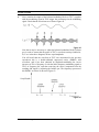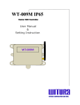
1
DSB/SSB Transmitter & Receiver Trainer ST2201 & ST2202 Operating Manual Ver.1.1 An ISO 9001 : 2000 company 94-101, Electronic Complex Pardeshipura, Indore- 452010, India Tel : 91-731- 2570301/02, 4211100 Fax: 91- 731- 2555643 email : [email protected] Website : www.scientech.bz Toll free : 1800-103-5050 ST2201 & ST2202 Scientech Technologies Pvt. Ltd. 2 ST2201 & ST2202 DSB/SSB Transmitter & Receiver Trainer ST2201 & ST2202 1 2 3 4 5 6 7 8 9 10 11 12 13. 14. Table of Contents ST2201 Features ST2201 Technical Specifications ST2202 Features ST2202 Technical Specifications Frequency components of Human voice A Simple Communication System Amplitude Modulation Carrier Wave Modulators Output Amplifier DSB Receiver Automatic Gain Control • Experiment 1 Double Sideband AM Generator • Experiment 2 To calculator modulation index of DSB wave by Trapezoidal Pattern • Experiment 3 Double Sideband AM Reception • Experiment 4 Study of Diode Detector Single Side Band Transmission • Experiment 5 Signal Sideband AM Generator • Experiment 6 Single Sideband AM Reception • Experiment 7 Operation of the Automatic Gain Control Circuit (AGC) Receiver Characteristics (Selectivity, Sensitivity, Fidelity) • 14. 15. 16. Experiment 8 To plot Selectivity Curve for Radio Receiver • Experiment 9 To plot Sensitivity Curve for Radio Receiver • Experiment 10 To plot Fidelity Curve for Radio Receiver Adjustment of Tuned Circuits Warranty List of Accessories Scientech Technologies Pvt. Ltd. 4 5 6 7 8 9 10 15 16 16 19 25 26 30 31 41 41 45 53 59 61 64 65 66 67 3 ST2201 & ST2202 Features • A self contained Trainer. • Functional blocks indicated on board mimic. • Input-output and Test Points provided onboard. • Built in DC Power Supply. • Fully documented student work book & operating manual. • 8 Switched faults. • Crystal controlled carrier frequency. • On-board audio, modulator, carrier frequency generation, antenna & speaker. • Compact size. Scientech Technologies Pvt. Ltd. 4 ST2201 & ST2202 Technical Specifications Audio Oscillator : With adjustable Amplitude & Frequency (300Hz-3.4 KHz) Audio Output : Audio amplifier with speaker Modulators : 2 nos. Balanced modulators with Band pass filter (1MHz) Carrier Frequency : 1 MHz Crystal controlled Transmitter Output : On board output amplifier (Gain Adjustable) 1. DSB--1 MHz 2. SSB--1.455 MHz Connected to Antenna / Cable Switched Faults : 8 Nos Power Supply : 230V +/- 10%, 50Hz Test Points : 27 Power Consumption : 4VA (approximately) Interconnections : 4 mm Banana sockets Dimensions (mm) : W 419 x H 90 x D 255 Weight : 2.8Kgs. (Approximately) Scientech Technologies Pvt. Ltd. 5 ST2201 & ST2202 Features • A self contained Trainer. • Functional blocks indicated on board mimic. • Input-output and Test Points provided onboard. • Built in DC Power Supply. • Fully documented student work book & operating manual. • 8 Switched Faults. • On board audio, modulators, detectors, amplitude limiter & filter circuits. • Effect of noise on the detection of FM signal may be investigated. • Compact size. Scientech Technologies Pvt. Ltd. 6 ST2201 & ST2202 Technical Specifications Construction : Super heterodyne Frequency Range : 980 KHz to 2.060 MHz Intermediate Frequency (IF) : 455 KHz Input Circuits : Tuning : 1. RF amplifier 2. Mixer 3. Local oscillator 4. Beat frequency oscillator 5. IF amplifier 1 6. IF amplifier 2 With variable capacitor (ganged) dial marking on board Receiving media : Telescopic antenna / RF cable Detector Circuits : 1. 2. Audio Output : Audio amplifier with speaker & headphone Automatic Gain Control : Switchable Switched Faults : 8 Nos. Power Supply : 230V ±10%, 50Hz Test Points : 50 Nos. Power Consumption : 3VA (approximately) Interconnections : 4mm Banana sockets Dimensions (mm) : W 419 x H 90 x D 255 Weight : 2.8Kg. (Approximately) Scientech Technologies Pvt. Ltd. Diode detector (DSB) Product detector (SSB) 7 ST2201 & ST2202 Frequency Components of Human Voice When we speak, we generate a sound that is very complex and changes continuously so at a particular instant in time the waveform may appear as shown in Figure 1 below. Figure 1 However complicated the waveform looks, we can show that it is made of many different sinusoidal signals added together. To record this information we have a choice of three methods. The first is to show the original waveform as we did in Figure 1. The second method is to make a list of all the separate sinusoidal waveforms that were contained within the complex waveform (these are called 'components', or 'frequency components'). This can be seen in Figure 2. Figure 2 Only four of the components of the audio signal in Figure 1 are shown in Figure 2. The actual number of components depends on the shape of the signal being considered and could be a hundred or more if the waveform was very complex. The third way is to display all the information on a diagram. Such a diagram shows the frequency spectrum. It is a graph with amplitude plotted against frequency. Each separate frequency is represented by a signal vertical line, the length of which represents the amplitude of the sinewave. Such a diagram is shown in Figure 3 below. Scientech Technologies Pvt. Ltd. 8 ST2201 & ST2202 Note that nearly all speech information is contained within the frequency range of 300 Hz to 3.4 KHz. Figure 3 Although an oscilloscope will only show the original complex waveform, it is important for us to remember that we are really dealing with a group of sinewaves of differing frequencies, amplitudes and phases. A Simple Communication System Once we are out of shouting range of another person, we must rely on some communication system to enable us to pass information. The essential parts of any communication system are transmitter, a communication link and a receiver, and in the case of speech, this can be achieved by a length of cable with a microphone and an amplifier at one end and a loudspeaker and an amplifier at the other. Simple Communication System Figure 4 For long distances, or for when it is required to send signals to many destinations at the same time, it is convenient to use a radio communication system. Scientech Technologies Pvt. Ltd. 9 ST2201 & ST2202 Amplitude Modulation (AM) The method that we are going to use is called amplitude modulation. As the name suggest, we are going to use the information signal to control the amplitude of the carrier wave. As the information signal increases in amplitude, the carrier wave, is also made to increase in amplitude. Likewise, as the information signal decreases, then the carrier amplitude decreases. By looking at Figure 5 below, we can see that the modulated carrier wave does appear to 'contain' in some way the information as well as the carrier. We will see later how the receiver is able to extract the information from the amplitude modulated carrier wave. Figure 5 Depth of Modulation : The amount by which the amplitude of the carrier wave increases and decreases depends on the amplitude of the information signal and is called the 'depth of modulation'. The depth of modulation can be quoted as a fraction or as a percentage. Percentage modulation = V max− V min x 100% V max + V min Here is an example, Figure 6 Scientech Technologies Pvt. Ltd. 10 ST2201 & ST2202 In above Figure 6 we can see that the modulated carrier wave varies from a maximum peak-to-peak value of 10 volts, down to a minimum value of 6 volts. Inserting these figure in the above formula, we get: Percentage modulation = 10 − 6 x 100% 10 + 6 = 4 x 100 % 16 = 25% or 0.25 The Frequency Spectrum : Assume a carrier frequency (fc) of 1 MHz and amplitude of, say 5 volts peak-to-peak. The carrier could be shown as, Figure 7 If we also have a 1 KHz information signal, or modulating frequency (fm), with amplitude of 2V peak-to-peak it would look like this, Figure 8 When both signals have passed through the amplitude modulator they are combined to produce an amplitude modulated wave. Scientech Technologies Pvt. Ltd. 11 ST2201 & ST2202 The resultant AM signal has a new frequency spectrum as shown in Figure 9 inserting changes that occurs as a result of the modulation process : 1. The original 1 KHz information frequency has disappeared. 2. The 1 MHz carrier is still present and is unaltered. Figure 9 There are two new components : 1. Carrier frequency (fc) plus the information frequency, called the upper side frequency (fc + fm). 2. Carrier frequency (fc) minus the information frequency, called the lower side frequency (fc - fm). The resulting signal in this example has a maximum frequency of 1001 KHz and a minimum frequency of 999 KHz and so it occupies a range of 2 KHz. This is called the bandwidth of the signal. Notice how the bandwidth is twice the highest frequency contained in the information signal. Sidebands : If the information signal consisted of range of frequencies, each separate frequency will create its own upper side frequency and lower side frequency. As an example, let us imagine that a carrier frequency of 1 MHz is amplitude modulated by an information signal consisting of frequencies 500Hz, 105 KHz and 2 KHz. As each modulating frequency produces its own upper and lower side frequency there is a range of frequencies present above and below the carrier frequency. All the upper side frequencies are grouped together and referred to as the upper sideband (USB) and all the lower side frequencies from the lower sideband (LSB). This amplitude modulated wave would have a frequency spectrum as shown in Figure 10. Scientech Technologies Pvt. Ltd. 12 ST2201 & ST2202 Figure 10 The Power in Sidebands : The modulated carrier wave that is finally transmitted contains the original carrier and the sidebands. The carrier wave is unaltered by the modulation process and contains at least two thirds of the total transmitted power. The remaining power is shared between the two sidebands. The power distribution depends on the depth of modulation used and is given by : Total power = (carrier power) (1+N2) 2 Where N is the depth of modulation. The greater the depth of modulation, the greater is the contained within the sidebands. The highest usable depth of modulation is 100% (above this the distortion becomes excessive). Since, at least twice as much power is wasted as is used, this form of modulation is not very efficient when considered on a power basis. The good news is that the necessary circuits at the transmitter and the receiver are simple and in expensive to design and construct. The double sideband transmitter : The transmitter circuits produce the amplitude modulated signals which are used to carry information over the transmission to the receiver. The main parts of the transmitter are shown in Figure 11. In Figure 11 & 12, we can see that the peak-to-peak voltage in the AM waveform increase and decrease in sympathy with the audio signal. Scientech Technologies Pvt. Ltd. 13 ST2201 & ST2202 AM Transmitter System Figure 11 To emphasize the connection between the information and the final waveform, a line is sometimes drawn to follow the peaks of the carrier wave as shown in Figure 12. This shape, enclosed by a dashed line in out diagram, is referred to as an 'envelope', or a 'modulation envelope' Figure 12 It is important to appreciate that it is only a guide to emphasize of the AM waveform. Information Signal : We have a choice of information signals on ST2201. We can use the signal provided in the audio oscillator or audio signal by connecting microphone to external audio input and keeping the audio input select switch in ext. position. In test situations it is more satisfactory to use a simple sinusoidal information signal since its attributes are known and of constant value. We can then measure various characteristics of the resultant. AM waveform, such as the modulation depth for example. Such measurements would be very difficult if we were using a varying signal from an external source such as a broadcast station. Scientech Technologies Pvt. Ltd. 14 ST2201 & ST2202 Carrier Wave The carrier wave must meet two main criteria. It should be of a convenient frequency to transmit over the communication path in use. In a radio link transmissions are difficult to achieve at frequencies less than 15 KHz and few radio links employ frequencies above 10GHz. Outside of this range the cost of the equipment increases rapidly with very few advantages. Remember that although 15 KHz is within the audio range, we cannot hear the radio signal because it is an electromagnetic wave and our ears can only detect waves which are due to changes of pressure. The second criteria is that the carrier wave should also be a sinusoidal waveform because a sinusoidal signal contains only a single frequency and when modulated by a signal frequency, will give rise to just two side frequencies, the upper and the lower side frequencies. However, if the sinewave were to be a complex wave containing many different frequencies, each separate frequency component would generate its own side frequencies. The result is that the overall bandwidth occupied by the transmission would be very wide and on the radio, would cause interference with the adjacent stations. In Figure 13, a simple case is illustrated in which the carrier only contains three frequency components modulated by a single frequency component. Even so we can see that the over all bandwidth has been considerably increased. If the carrier contained several frequencies, each would produce its own side frequencies Figure 13 Scientech Technologies Pvt. Ltd. 15 ST2201 & ST2202 Modulator In this circuit, the amplitude of the carrier is increased and decreased in sympathy with the incoming information signal. AM Modulation Process Figure 14 The modulated signal is now nearly ready for transmission. If the modulation process has given rise to any unwanted frequency components then a band pass filter can be employed to remove them. Output Amplifier This amplifier is used to increase the strength of the signal before being passed to the antenna for transmission. The output power contained in the signal and the frequency of transmission are the two main factors that determine the range of the transmission. The Antenna : An electromagnetic wave, such as a light ray, consists of two fields, an electric field and magnetic field. These two fields are always as right angles to each other and move in a direction which is at right angles to both the magnetic and the electric fields, this is shown in Figure 15, 16 & 17. Figure 15 shows the electric fields moving out from the antenna. In this example the electric field is vertical because the antenna is positioned vertically (in the direction shown by y). Figure 16 shows magnetic field is always at right angles to the electric field so in this case, it is positioned horizontally (in the direction shown by x). Figure 17 shows an electromagnetic wave both fields exist together and they move at the speed of light in a direction that is at right angles to both fields (shown by the arrow labeled z). Scientech Technologies Pvt. Ltd. 16 ST2201 & ST2202 Figure 15 This shows the electric field moving out from the antenna. In this example the electric field is vertical because the antenna is positioned vertically (in the direction shown by y). Figure 16 The magnetic field is always at right angles to the electric field so in this case, it is positioned horizontally (in the direction shown by x). Figure 17 In an electromagnetic wave both fields exist together and they move at the speed of light in a direction that is at right angles to both fields (shown by the arrow labeled z). The antenna converts the power output of the output amplifier into an electromagnetic wave. Scientech Technologies Pvt. Ltd. 17 ST2201 & ST2202 How does it do this ? The output amplifier causes a voltage to be generated along the antenna thus generating a voltage difference and the resultant electric field between the top and bottom. This causes an alternating movement of electrons on the transmitting antenna which is really an AC current. Since an electric current always has a magnetic field associated with it, an alternating magnetic field is produced. The overall effect is that the output amplifier has produced alternating electric and magnetic fields around the antenna. The electric and magnetic fields spread out as an electromagnetic wave at the speed of light (3 x 10⁸ meters per second). For maximum efficiency, the antenna should be of a precise length. The optimum size of antenna for most purposes is one having an overall length of one quarter of the wave length of the transmitted signal. This can be found by, v µ = f Where v = speed of light. µ = wave length and f = frequency in Hertz. In the case of the ST2201, the transmitted carrier is 1 MHz and so the ideal length of antenna is : 3 x 10⁸ µ = 1 x 10⁶ µ = 300m. One quarter of this wavelength would be 75meters (about 245 feet). We can now see that the antenna provided on the ST2201 is necessarily less than the ideal size! Polarization : If the transmitting antenna is placed vertically, the electrical field is vertical and the magnetic field is horizontal (as seen in Figure 15, 16 & 17). If the transmitting antenna is now moved by 90° to make it horizontal, the electrical field is horizontal and the magnetic field becomes vertical. By convention, we use the plane of the electric field to describe the orientation, or polarization, of the 'em' (electromagnetic) wave. A vertical transmitting antenna results in a vertically polarized wave, and a horizontal one would result in a horizontally polarized 'em' wave. Scientech Technologies Pvt. Ltd. 18 ST2201 & ST2202 DSB Receiver The 'em' wave from the transmitting antenna will travel to the receiving antenna carrying the information with it. DSB Receiver Figure 18 We will continue to follow our information signal as it passes through the receiver. The Receiving Antenna : The receiving antenna operates in the reverse mode to the transmitter antenna. The electromagnetic wave strikes the antenna and generates a small voltage in it. Ideally, the receiving antenna must be aligned to the polarization of the incoming signal so generally, a vertical transmitting antenna will be received best by using a vertical receiving antenna. The actual voltage generated in the antenna is very small-usually less than 50 millivolts and often only a few microvolts. The voltage supplied to the loudspeaker at the output of the receiver is upto ten volts. We clearly need a lot of amplification. Radio Frequency (RF) Amplifier : The antenna not only provides very low amplitude input signals but it picks up all available transmissions at the same time. This would mean that the receiver output would include all the various stations on top of each other which would make it impossible to listen to any one transmission. The receiver circuits generate noise signals, which are added to the wanted signals. We hear this as a 'background hiss' and are particularly noticeable if the receiver is tuned between stations or if a weak station is being received. The RF amplifier is the first stage of amplification. It has to amplify the incoming signal above the level of the internally generated noise and also to start the process of selecting the wanted station and rejecting the unwanted ones. Selectivity : A parallel tuned circuit has its greatest impedance at resonance and decreases at higher and lower frequencies. If the tuned circuit is included in the circuit design of an amplifier, it results in an amplifier which offers more gain at the frequency of resonance and reduced amplification above and below this frequency. This is called Selectivity. Scientech Technologies Pvt. Ltd. 19 ST2201 & ST2202 Figure 19 The radio receiver is tuned to a frequency of 820 KHz and, at this frequency; the amplifier provides a gain of five. Assuming the incoming signal has an amplitude of 10 mV as shown, its output at this frequency would be 5 x 10mV = 50mV. The stations being received at 810 KHz and 830 KHz each have a gain of one. With the same amplitude of 10m V, this could result in outputs of 1 x 10mV = 10mV. The stations at 800 KHz and 840 KHz are offered a gain on only 0.1 (approx). This means that the output signal strength would be only 0.1 x 10mV = 1mV. The over all effect of the selectivity is that the incoming signals each have the same amplitude, the outputs vary between 1mV and 50mV so we can select, or 'tune', the amplifier to pick out the desired station. The greatest amplification occurs at the resonance frequency of the tuned circuit. This is sometimes called the center frequency. In common with nearly all radio receivers, ST2202 adjusts the capacitor value by means of the tuning control to select various signals. Scientech Technologies Pvt. Ltd. 20 ST2201 & ST2202 The Local Oscillator : This is an oscillator producing a sinusoidal output similar to the carrier wave oscillator in the transmitter. In this case however, the frequency of its output is adjustable. The same tuning control is used to adjust the frequency of both the local oscillator and the center frequency of the RF amplifier. The local oscillator is always maintained at a frequency which is higher, by a fixed amount, then the incoming RF signals. The local oscillator frequency therefore follows, or tracks, the RF amplifier frequency. This will prove to be very useful as we will see in the next section. Mixer : The mixer performs a similar function to the modulator in transmitter. We may remember that the transmitter modulator accepts the information signal and the carrier frequency, and produces the carrier plus the upper and lower sidebands. The mixer in the receiver combines the signal from the RF amplifier and the frequency input from the local oscillator to produce three frequencies: 1. A 'difference' frequency of local oscillator frequency - RF signal frequency. 2. A 'sum' frequency equal to local oscillator frequency + RF signal frequency 3. A component at the local oscillator frequency. Mixing two signals to produce such components is called a 'heterodyne' process. When this is carried out at frequencies which are above the audio spectrum, called 'supersonic' frequencies, the type of receiver is called a ‘super heterodyne' receiver. It is not a modern idea having been invented in the year 1917. From RF amplifier To IF amplifier From local oscillator Figure 20 In the section the local oscillator, we read how the local oscillator tracks the RF amplifier so that the difference between the two frequencies is maintained at a constant value. In ST2201 & ST2202 this difference is 455 KHz (approximately). As an example, if the radio is tuned to receive a broadcast station, which transmits at 800 KHz, the local oscillator will be running at 1.25 MHz. The difference frequency is 1.255MHz - 800 MHz = 455 KHz. Scientech Technologies Pvt. Ltd. 21 ST2201 & ST2202 If the radio is now re-tuned to receive a different station being broadcast on 700 KHz, the tuning control re-adjusts the RF amplifier to provide maximum gain at 700 KHz and the local oscillator to 1.155 MHz. The difference frequency is still maintained at the required 455 KHz. This frequency difference therefore remains constant regardless of the frequency to which the radio is actually tuned and is called the intermediate frequency (IF). Figure 21 Note : In Figure 21, the local oscillator output is shown larger than the IF and RF frequency components, this is usually the case. However, there is no fixed relationship between the actual amplitudes. Similarly, the IF and RF amplitudes are shown as being equal in amplitude but again there is no significance in this. Image Frequencies : In the last section, we read we could receive a station being broadcast on 700 KHz by tuning the local oscillator to a frequency of 1.155 MHz. thus giving the difference (IF) frequency of required 455 KHz. What would happen if we were to receive another station which was broadcasting on a frequency of 1.61 MHz? This would also mix with the local oscillator frequency of 1.155 MHz to produce the required IF frequency of 455 KHz. This would mean that this station would also be received at the same time as our wanted one at 700 KHz. Station 1 : Frequency 700 KHz, Local oscillator 1.155 MHz, IF = 455 KHz Station 2 : Frequency 1.61 MHz, oscillator 1.155 MHz, IF = 455 KHz An 'image frequency' is an unwanted frequency that can also combine with the Local Oscillator output to create the IF frequency. Scientech Technologies Pvt. Ltd. 22 ST2201 & ST2202 Notice how the difference in frequency between the wanted and unwanted stations is twice the IF frequency. In the ST2201/ST2202, it means that the image frequency is always 910 KHz above the wanted station. This is a large frequency difference and even the poor selectivity of the RF amplifier is able to remove the image frequency unless it is very strong. In this case, it will pass through the receiver and will be heard at the same time as the wanted station. Frequency interactions between the two stations tend to cause irritating whistles from the loudspeaker. Intermediate Frequency Amplifier (IF Amplifiers) : The IF Amplifier in this receiver consists of two stages of amplification and provides the main signal amplification and selectivity. Operating at a fixed IF frequency means that the design of the amplifiers can be simplified. If it were not for the fixed frequency, all the amplifiers may need to be tunable across the whole range of incoming RF frequencies and it would be difficult to arrange for all the amplifiers to keep in step as they are re-tuned. In addition, the radio must select the wanted transmission and reject all the others. To do this the band pass of all the stages must carefully controlled. Each IF stage does not necessarily have the same band pass characteristics. The overall response is important. Again, this is something which is much more easily achieved without the added complication of making them tunable. At the final output from the IF amplifiers, we have a 455 KHz wave which is amplitude modulated by the wanted audio information. The selectivity of the IF amplifiers has removed the unwanted components generated by the mixing process. Diode Detector : The function of the diode detector is to extract the audio signal from the signal at the output of the IF amplifiers. It performs this task in a very similar way to a half wave rectifier converting an AC input to a DC output. Figure 22 shows a simple circuit diagram of the diode detector. Figure 22 Scientech Technologies Pvt. Ltd. 23 ST2201 & ST2202 In Figure 22, the diode conducts every time the input signal applied to its anode is more positive than the voltage on the top plate of the capacitor. When the voltage falls below the capacitor voltage, the diode ceases to conduct and the voltage across the capacitor leaks away until the next time the input signal is able to switch it on again. See Figure 23. Figure 23 The result is an output which contains three components : 1. The wanted audio information signal. 2. Some ripple at the IF frequency. 3. A positive DC voltage level. The Audio Amplifier : At the input to the audio amplifier, a low pass filter is used to remove the IF ripple and a capacitor blocks the DC voltage level. Figure 24 shows the result of the information signal passing through the diode detector and audio amplifier. The input to the diode detector from the last IF amplifier Output of diode detector includes : a DC level, the audio signal, ripple at IF frequency Output after filtering Figure 24 The remaining audio signals are then amplified to provide the final output to the loudspeaker. Scientech Technologies Pvt. Ltd. 24 ST2201 & ST2202 Automatic Gain Control (AGC) The AGC circuit is used to prevent very strong signals from overloading the receiver. It can also reduce the effect of fluctuations in the received signal strength. The 'AGC circuit makes use of the mean DC voltage level present at the output of the diode detector. If the signal increases, the mean DC voltage level also increases, IF the mean DC voltage level exceeds a predetermined threshold value, a voltage is applied to the RF and IF amplifiers in such a way as to decrease their gain to prevent overload. As soon as the incoming signal strength decreases, such that the mean DC voltage level is reduced below the threshold, the RF and IF amplifiers return to their normal operation. AGC Off : At low signal strength the AGC circuit has no effect This part of the transmission will overload the receiver and cause distortion AGC On : The AGC has limited the amplification to prevent overload and distortion Figure 25 Recommended testing instruments for experimentation : 1. 20MHz, dual trace oscilloscope 201. 2. Switchable probe. 3. Function Generator (1 MHz). 4. Frequency Counter (10 MHz) preferable. Scientech Technologies Pvt. Ltd. 25 ST2201 & ST2202 Experiment 1 Objective : Double Sideband AM Generation Procedure : This experiment investigates the generation of double sideband amplitude modulated (AM) waveforms, using the ST2201 module. By removing the carrier from such an AM waveforms, the generation of double sideband suppressed carrier (DSBSC) AM is also investigated. To avoid unnecessary loading of monitored signals, X10 oscilloscope probes should be used throughout this experiment. 1. Ensure that the following initial conditions exist on the board. a. Audio input select switch should be in INT position: b. Mode switch in DSB position. c. Output amplifier's gain potentiometer in full clockwise position. d. Speakers switch in OFF position. 2. Turn on power to the ST2201 board. 3. Turn the audio oscillator block's amplitude pot to its full clockwise (MAX) position, and examine the block's output (TP14) on an oscilloscope. This is the audio frequency sine wave which will be as our modulating signal. Note that the sine wave’s frequency can be adjusted from about 300 Hz to approximately 3.4 KHz, by adjusting the audio oscillator's frequency potentimeter. Note also that the amplitude of this audio modulating signal can be reduced to zero, by turning the Audio oscillator's amplitude present to its fully counterclockwise (MIN) position. Return the amplitude present to its max position. 4. Turn the balance pot, in the balanced modulator & band pass filter circuit 1 block, to its fully clockwise position. It is this block that we will use to perform double-side band amplitude modulation. 5. Monitor, in turn, the two inputs to the balanced modulator & band pass filter circuits 1 block, at TP1 and TP9. Note that: a. The signal at TP1 is the audio-frequency sinewave from the audio oscillator block. This is the modulating input to our double-sideband modulator. b. Test Point 9 carries a sine wave of 1MHz frequency and amplitude 120mVpp approx. This is the carrier input to our double-sideband modulator. Scientech Technologies Pvt. Ltd. 26 ST2201 & ST2202 6. Next, examine the output of the balanced modulator & band pass filter circuit 1 block (at tp3), together with the modulating signal at TP1 Trigger the oscilloscope on the TP1 signal. Check that the waveforms as shown in Figure 26 Figure 26 The output from the balanced modulator & band pass filter circuit 1 block (at TP3) is a double-sideband. AM waveform, which has been formed by amplitude-modulating the 1MHz carrier sinewave with the audio-frequency sinewave from the audio oscillator. The frequency spectrum of this AM waveform is as shown below in Figure 27, where fm is the frequency of the audio modulating signal. Figure 27 7. To determine the depth of modulation, measure the maximum amplitude (Vmax) and the minimum amplitude (V min) of the AM waveform at TP3, and use the following formula: Percentage Modulation = Vmax − Vmin Vmax + Vmin Where V max and V min are the maximum and minimum amplitudes shown in Figure 26. Scientech Technologies Pvt. Ltd. 27 ST2201 & ST2202 8. Now vary the amplitude and frequency of the audio-frequency sinewave, by adjusting the amplitude and frequency present in the audio oscillator block. Note the effect that varying each pot has on the amplitude modulated waveform. The amplitude and frequency amplitudes of the two sidebands can be reduced to zero by reducing the amplitude of the modulating audio signal to zero. Do this by turning the amplitude pot to its MIN position, and note that the signal at TP3 becomes an un-modulated sine wave of frequency 1 MHz, indicating that only the carrier component now remains. Return the amplitude pot to its maximum position. Now turn the balance pot in the balanced modulator & band pass filter circuit 1 block, until the signal at TP3 is as shown in Figure 28 Figure 28 The balance pot varies the amount of the 1 MHz carrier component, which is passed from the modulator's output. By adjusting the pot until the peaks of the waveform (A, B, C and so on) have the same amplitude, we are removing the carrier component altogether. We say that the carrier has been 'balanced out' (or 'suppressed') to leave only the two sidebands. Note that once the carrier has been balanced out, the amplitude of TP3's waveform should be zero at minimum points X, Y; Z etc. If this is not the case, it is because one of the two sidebands is being amplified more than the other. To remove this problem, the band pass filter in the balanced modulator & band pass filter circuit 1 block must be adjusted so that it passes both sidebands equally. This is achieved by carefully trimming transformer T1, until the waveform's amplitude is as close to zero as possible at the minimum points. The waveform at TP3 is known as a double-side suppressed carrier (DSBSC) waveform, and its frequency spectrum is as shown in Figure 29. Scientech Technologies Pvt. Ltd. 28 ST2201 & ST2202 Frequency Spectrum of DSBSC Wave Form Figure 29 Note that now only the two sidebands remain, the carrier component has been removed. 9. Change the amplitude and frequency of the modulating audio signal (by adjusting the audio oscillator block's amplitude and frequency pots), and note the effect that these changes on the DSBSC waveform. The amplitudes of the two sidebands can be reduced to zero by reducing the amplitude of the modulating audio signal to zero. Do these by turning the amplitude present to its MIN position, and note that the monitored signal becomes a D C level, indicating that there .are now no frequency components present. Return the amplitude pot to its MAX position. 10. Examine the output from the output amplifier block (TP13), together with the audio modulating signal (at TP1), triggering the scope with the audio modulating signal. Note that the DSBSC waveform appears, amplified slightly at TP13, as we will see later, it is the output amplifier's output signal which will be transmitted to the receiver. 11. By using the microphone, the human voice can be used as the modulating signal, instead of using ST2201's audio oscillator block. Connect the module's output to the external audio input on the ST2201 board, and put the audio input select switch in the ext position. The input signal to the audio input module may be taken from an external microphone or from a cassette recorder, by choosing the appropriate switch setting on the module. Refer the user manual for the audio input module, for further details. Scientech Technologies Pvt. Ltd. 29 ST2201 & ST2202 Experiment 2 Objective : To calculate modulation index of DSB wave by trapezoidal pattern. Procedure : 1. Perform the experiment number 1 upto step number 6 2. Now apply the modulated waveform to the Y input of the Oscilloscope and the modulating signal to the X input. 3. Press the XY switch, you will observe the waveform similar to the one given below: Figure 30 Calculate the modulation index by substituting in the formula Percentage Modulation = 4. V max - V min V max + V min Some common trapezoidal patterns for different modulation indices are as shown: Figure 31 Scientech Technologies Pvt. Ltd. 30 ST2201 & ST2202 Experiment 3 Objective : Double Sideband AM Reception Procedure : This experiment investigates the reception and demodulation of AM waveforms by the ST2201/ ST2202 module. Both AM broadcast signals, and AM transmissions from ST2201, will be examined, and the operation of automatic gain control at the receiver will be investigated. To avoid unnecessary loading of monitored signals, X10 oscilloscope probes should be used throughout this experiment. 1. Position the ST2201 & ST2202 modules, with the ST2201 board on the left, and a gap of about three inches between them. 2. Ensure that the following initial conditions exist on the ST2201 board. 3. 4. a. Audio oscillator's amplitude pot in fully clockwise position. b. Audio input select switch in INT position. c. Balance pot in balanced modulator & band pass filter circuit 1 block, in full clockwise position; d. Mode switch in DSB position. e. Output amplifier's gain pot in full counter-clockwise position. f. TX output select switch in ANT position: g. Audio amplifier’s volume pot in fully counter-clockwise position. h. Speaker switch in ON position. i. On-board antenna in vertical position, and fully extended. Ensure that the following initial conditions exist on the ST2102 board: a. RX input select switch in ANT position. b. R.F. amplifier's tuned circuit select switch in INT position. c. R.E amplifier's gain pot in fully clock-wise position; d. AGC switch in INT position. e. Detector switch in diode position. f. Audio amplifier's volume pot in fully counter-clockwise position. g. Speaker switch in ON position. h. Beat frequency oscillator switch in OFF position. i. On-board antenna in vertical position, and fully extended. Turn on power to the modules. Scientech Technologies Pvt. Ltd. 31 ST2201 & ST2202 5. On the ST2202 module, slowly turn the audio amplifier's volume pot clockwise, until sounds can be heard from the on-board loudspeaker. Next, turn the vernier tuning dial until a broad cast station can be heard clearly, and adjust the volume control to a comfortable level. Note : If desired, headphones (supplied with the module) may be used instead of the on-board loudspeaker. To use the headphones, simply plug the headphone jack into the audio amplifier block's headphones socket, and adjust controlled block's volume pot. 6. The first stage or 'front end' of the ST2202 AM receiver is the R.F amplifier stage. This is a wide -bandwidth tuned amplifier stage, which is tuned into the wanted station by means of the tuning dial. Once it has been tuned into the wanted station, the R.F. amplifier, having little selectivity, will not only amplify, but also those frequencies that are close to the wanted frequency. As we will see later, these nearby frequencies will be removed by subsequent stages of the receiver, to leave only the wanted signal. Examine the envelope of the signal at the R.F. amplifier's output (at TP12), with an a.c. - coupled oscilloscope channel. Note that : a. The amplifier's output signal is very small in amplitude (a few tens of millivolts at the most). This is because one stage of amplification is not sufficient to bring the signal's amplitude up to a reasonable level. b. Only a very small amount of amplitude modulation can be detected, if any. This is because there are many unwanted frequencies getting through to the amplifier output, which tend to 'drown out' the wanted AM Signal. You may notice that the waveform itself drifts up and down on the scope display, indicating that the waveform's average level is changing. This is due to the operation of the AGC circuit, which will be explained later. 7. The next stage of the receiver is the mixer stage, which mixes the R.F. amplifier's output with the output of a local oscillator. The Frequency of the local oscillator is also tuned by means of the tuning dial, and is arranged so that its frequency is always 455 KHz above the signal frequency that the R.F. amplifier is tuned to. This fixed frequency difference is always present, irrespective of the position of the tuning dial, and is arranged so that its frequency is always 455 KHz above the signal frequency that the R.F. amplifier is tuned to. This fixed frequency difference is always present, irrespective of the position of the tuning dial, and is known as the intermediate frequency (IF for short). This frequency relationship is shown below, for some arbitrary position of the tuning dial. Scientech Technologies Pvt. Ltd. 32 ST2201 & ST2202 Figure 32 Examine the output of the local oscillator block, and check that its frequency varies as the tuning dial is turned. Re-time the receiver to a radio station. 8. The operation of the mixer stage is basically to shift the wanted signal down to the IF frequency, irrespective of the position of the tuning dial. This is achieved in two stages. a. By mixing the local oscillator's output sinewave with the output from the R.F. amplifier block. This produces three frequency components : The local oscillator frequency = (f sig + IF) The sum of the original two frequencies, f sum = (2 f sig + IF) The difference between the original two frequencies, f diff = (f sig + IF - f sig) = IF These there frequency components are shown in Figure 33. Figure 33 b. By strongly attenuating all components. except the difference frequency, IF this is done by putting a narrow-bandwidth band pass filter on the mixer's output. Scientech Technologies Pvt. Ltd. 33 ST2201 & ST2202 The end result of this process is that the carrier frequency of the selected AM station is shifted down to 455 KHz (the IF Frequency), and the sidebands of the AM signal are now either side of 455 KHz. 9. Note that, since the mixer's band pass filter is not highly selective, it will not completely remove the local oscillators and sum frequency components from the mixer's output. this is the case particularly with the local oscillator component, which is much larger in amplitude than the sum and difference components. Examine the output of the mixer block (TP20) with an a.c. coupled oscilloscope channel, and note that the main frequency component present changes as the tuning dial is turned. This is the local oscillator component, which still dominates the mixer's output, in spite of being attenuated by the mixer's band pass filter. 10. Tune in to a strong broadcast station again and note that the monitored signal shows little, if any, sign of modulation. This is because the wanted component, which is now at the IF frequency of 455 KHz, is still very small in component, which is now at the IF frequency of 455 KHz, is still very small in comparison to the local oscillator component. What we need to do now is to preferentially amplify frequencies around 455 KHz, without amplifying the higher-frequency local oscillator and SUM components. This selective amplification is achieved by using two IF amplifier stages, IF amplifier 1 and IF amplifier 2, which are designed to amplify strongly a narrow band of frequencies around 455 KHz, without amplifying frequencies on either side of this narrow band. These IF amplifiers are basically tuned amplifiers which have been pre-tuned to the IF frequency-they have a bandwidth just wide enough to amplify the 455 KHz carrier and the AM sidebands either side of it. Any frequencies outside this narrow frequency band will not be amplified. Examine the output of IF amplifier 1 (at. TP24) with an a.c.-coupled oscilloscope channel, and note that : a. The overall amplitude of the signal is much larger than the signal amplitude at the mixer's output, indicating that voltage amplification has occurred. b. The dominant component of the signal is now at 455 KHz, irrespective of any particular station you have tuned into. This implies that the wanted signal, at the IF frequency, has been amplified to a level where it dominates over the unwanted components. c. The envelope of the signal is modulated in amplitude, according to the sound information being transmitted by the station you have tuned into. Scientech Technologies Pvt. Ltd. 34 ST2201 & ST2202 11. Examine the output of IF amplifier 2 (TP28) with an a.c.-coupled oscilloscope channel, noting that the amplitude of the signal has been further amplified by this second IF amplitude of the signal has been further amplified by this second IF amplifier stage. IF amplifier 2 has once again preferentially amplified signals around the IF frequency (455 KHz), so that: a. The unwanted local oscillator and sum components from the mixer are now so small in comparison, that they can be ignored totally, b. Frequencies close to the I F frequency, which are due to stations close to the wanted station, are also strongly attenuated. The resulting signal at the output of IF amplifier 2 (TP28) is therefore composed almost entirely of a 455 KHz carrier, and the A.M. sidebands either side of it carrying the wanted audio information. 12. The next step is extract this audio information from the amplitude variations of the signal at the output of IF amplifier 2. This operation is performed by the diode detector block, whose output follows the changes in the amplitude of the signal at its input. To see how this works, examine the output of the diode detector block (TP31), together with the output from. IF amplifier 2 (at tp28). Note that the signal at the diode detector's output: 13. • Follows the amplitude variations of the incoming signal as required: • Contains some ripple at the IF frequency of 455 KHz, and • The signal has a positive DC offset, equal to half the average peak to peak amplitude of the incoming signal. We will see how we make use of this offset later on, when we look at automatic gain control (AGC). The final stage of the receiver is the audio amplifier block contains a simple low-pass filter which passes only audio frequencies, and removes the highfrequency ripple from the diode detector's output signal. This filtered audio signal is applied to the input of an audio power amplifier, which drives on board loudspeaker (and the headphones, if these are used). The final result is the sound you are listening to! The audio signal which drives the loudspeaker can be monitored at TP39 (providing that the audio amplifier block's volume pot is not in its minimum volume position). Compare this signal with that at the diode detector's output (TP31), and note how the audio amplifier block's low pass filter has 'cleaned up' the audio signal. You may notice that the output from the audio amplifier block (tp39) is inverted with respect to the signal at the output of the diode detector (TP31) this inversion is performed by the audio power amplifier IC, and in no way affects the sound produced by the receiver. Scientech Technologies Pvt. Ltd. 35 ST2201 & ST2202 14. Now that we have examined the basic principles of operation of the ST2202 receiver for the reception and demodulation of AM broadcast signals, we will try receiving the AM signal from the ST2201 transmitter. Presently, the gain of ST2201's output amplifier block is zero, so that there is no output from the Transmitter. Now turn the gain pot in ST2201's output amplifier block to its fully clockwise (maximum gain) position, so that the transmitter generates an AM signal. On the ST2201 module, examine the transmitter's output signal (TP13), together with the audio modulating signal (TP1), triggering the 'scope with the signal'. Since ST2201 TX output select switch is in the ANT position, the AM signal at tp13 is fed to the transmitter's antenna. Prove this by touching ST2201's antenna, and nothing that the loading caused by your hand reduces the amplitude of the AM waveform. at TP13. The antenna will propagate this AM signal over a maximum distance of about 1.4 feet. We will now attempt to receive the propagated AM waveform with the ST2201/ ST2202 board, by using the receiver's on board antenna. Note : If more than one ST2201 transmitter/receiver system is in use at one time, it is possible that there may be interference between nearby transmitters if antenna propagation is used. To eliminate this problem, use a cable between each transmitter/receiver pair, connecting it between ST2201's TX output socket and ST2201/ST2202's RX input socket. If you do this, make sure that the transmitter's TX output select switch, and the receiver's RX input select switch, are both in the SKT position, then follow the steps below as though antenna propagation were being used. 15. On the ST2201 module, turn the volume pot (in the audio amplifier block) clockwise, until you can hear the tone of the audio oscillator’s output signal, from the loudspeaker on the board. Note : If desired, headphones may be used instead of the loudspeaker on the board. To use the headphones, simply plug the headphone jack into the audio amplifier block's headphones socket, and put the speaker switch in the OFF position. The volume from the headphones is still controlled by the block's volume pot. Turn the volume pot to the full counter-clockwise (minimum volume) position. 16. On the ST2201/ST2202 receiver, adjust the volume pot so that the receiver's output can be clearly heard. Then adjust the receiver's tuning dial until the tone generated at the transmitter is also clearly audible at the receiver (this should be when the tuning dial is set to about 55-65 and adjust the receiver's volume pot until the tone is at a comfortable level. Check that you are tuned into the transmitter's output signal, by varying ST2201's frequency pot in the audio oscillator block, and nothing that the tone generated by the receiver changes. Scientech Technologies Pvt. Ltd. 36 ST2201 & ST2202 The ST2201/2202 receiver is now tuned into AM signal generated by the ST2201 transmitter. Briefly check that the waveforms, at the outputs of the following receiver blocks, are as expected : 17. R. F. Amplifier (TP12) Mixer (TP20) I.F. Amplifier 1 (TP24) I.F. Amplifier 2 (TP28) Diode Detector (TP31) Audio Amplifier (TP39) By using the microphone, the human voice can be used as transmitter's audio modulating signal, instead of using ST2201's audio oscillator block. Use DSB and not DSBSC. Connect the microphone’s output to the external audio input on the ST2201 board, and put the audio input select switch in the EXT position. An overview of DSB Transmission : A double sideband transmission was the first method of modulation developed and, for broadcast stations, is still the most popular. Indeed, for medium and long range broadcast stations, is still the most popular. Indeed, for medium and long range broadcast stations it is the only system in use. The reason for such widespread use is that the receiver design can be very simple and reliable. None of the characteristics are particularly critical so reception is still possible even in adverse conditions. In this context, a broadcast is information transmitted for entertainment or information and available for use by anyone with a receiver. It never requires a response or acknowledgement for the receiving station. So in many ways it is similar to a newspaper or magazine which is published and distributed to anyone who is interested in reading a copy. Radio is also used for communications in which the signal is addressed to a receiving station or a group of stations. Using the written word this would correspond to a private letter or perhaps business or military information being exchanged. For this type of communication other systems are used, one of which is investigated in this chapter. As we will see, there are two serious drawbacks to the DSB AM system. Scientech Technologies Pvt. Ltd. 37 ST2201 & ST2202 DSB is Wasteful of Power : The first problem is to do with the power distribution in a DSB amplitude modulated wave. The total power being transmitted is 1000+320+320 = 1640W Figure 34 How much of the DSB AM wave is really needed ? The whole purpose of the modulation system is to transfer information from one place to another. How efficiently does it to achieve this? We are transmitting two sidebands and a carrier. The carrier contains no useful information at all and yet contains over half the total power. This is clearly a waste. Even the sidebands can be improved. We can remember that combining the information signal and the carrier gave rise to an upper and a lower sideband, each of which contains a copy of the information being transmitted. There is no necessity to send two copies of the same information so this is a waste of power and bandwidth. Scientech Technologies Pvt. Ltd. 38 ST2201 & ST2202 Double Sideband Suppressed Carried Transmission (DSBSC) : If we avoid using the carrier frequency shown in Figure we would save ourselves 1KW of the transmitted power. The total power being transmitted is now reduced to 640W Figure 35 Well, the carrier has done its job-in the modulator. That is where we needed it to move or translate the audio signals up to radio frequency values which can be radiated by the antenna. This shifting, or translating of frequencies is the main function of a modulator. At the transmitter, the carrier can easily be removed by a band stop filter designed to eliminate the carrier frequency whilst allowing the two sidebands to be transmitted. At the receiver, the carrier must be re-inserted to produce the modulation envelope to enable the detector to extract the information signal. And here lies the problem. The carrier has to be re-inserted at exactly the correct frequency to reproduce the original AM waveform (within a few hertz). If it is not, there are serious problems with reception. Take a situation in which the upper and lower side frequencies are spaced 4 KHz either side of the carrier at : 600 - 4 = 596 KHz & 600 + 4 = 604 KHz. Now, let's assume that the receiver carrier were to be re-inserted at an incorrect value of 601 KHz. This would result in a spacing of only 3 KHz between the carrier and the upper side frequency and 5 KHz between the carrier and the lower side frequency. What effect would this have? Scientech Technologies Pvt. Ltd. 39 ST2201 & ST2202 Remembering our previous exercise in which we created an AM envelop by plotting a graph, we can see that these incorrect side frequency spacing will give rise to a badly deformed modulation envelop and hence a distorted output sound which makes speech sound like 'Donald Duck'. With this type of transmission, the receiver would be carefully tuned in to the correct frequency and the station would be received. A few moments later, the reinserted carrier frequency would drift slowly off tune and 'Donald Duck' would re-appear. We would have to reach over and retune the radio and settle back to enjoy the next few seconds of broadcast until the drift starts again. The frequency control necessary to ensure that the re-inserted carrier stays at exactly the correct value regardless of changes of temperature, vibration etc. would make the receiver too complex and expensive for domestic use. For this reason, DSBSC is very seldom used. Overall, the waste of transmitted power to send the carrier is less expensive than the additional cost of perhaps several million high quality receivers. Such receivers are used for professional (and amateur) communications but are expensive, between ten and a hundred times the cost of a standard radio receiver. Scientech Technologies Pvt. Ltd. 40 ST2201 & ST2202 Experiment 4 Objective : Study of Diode Detector Procedure : 1. Connect and make the settings as per experiment number 2 2. Observe the signal flow from the input of diode detector to anode of diode D6, at its cathode, after the filter and at the output at TP31. 3. Vary the preset R45 in the diode detector block while observing the output of diode detector. 4. You can see the variations in the detected output when you change the RC time constant of the filter formed by R45 and C32. Signal Side Band Transmission (SSB) This is just taking the previous reasoning to its ultimate conclusion. If we don't really need the carrier, we can leave it out and save power. This is DSBSC transmission. Just one step further and we can say that since both sidebands carry the same information, there is no point in transmitting both of them. It makes no difference which sideband is removed but in most systems the lower sideband is normally eliminated. We can simply transmit a single sideband as shown in Figure 36 and by comparing the power use with Figure 34, we can see a considerable power saving. The total power is now only 320W Figure 36 The bandwidth of an SSB system is equal to the range of frequencies present in the information waveform where as a DSB signal has a bandwidth twice as wide as the highest frequency component in the information signal. This also means a greatly reduced bandwidth for the system. In Figure 36 we are transmitting just a single frequency. Scientech Technologies Pvt. Ltd. 41 ST2201 & ST2202 The SSB Transmitter : The design of the SSB transmitter is accomplished in two stages. First we generate a DSBSC signal and then remove the lower sideband to achieve the final SSB result. Generating the DSBSC Signal : To do this, we use a balanced modulator. The principle of this circuit is shown in Figure 37. Figure 37 Internally, the balanced modulator generates the AM waveform which includes the carrier and both sidebands. It then offers the facility to feed a variable amount of the carrier back into the modulator in anti-phase to cancel the carrier output. In this way we can balance out the carrier to suppress it completely leaving just the required DSBSC waveform. From DSBSC to SSB : The DSBSC signal consists of the two sidebands, one of which can be removed by passing them through a band pass filter. On the ST2201 this is achieved as shown in Figure 38. Figure 38 Scientech Technologies Pvt. Ltd. 42 ST2201 & ST2202 The inputs to the balanced modulator comprise the audio inputs from the audio oscillator, which extend from 300Hz to 3.4 KHz, and the carrier input. On the ST2201 board this carrier oscillator, although marked as '455 KHz', actually needs to operate at a frequency which is a little less than this, around 453 KHz. Why is this? It is to ensure that the upper sideband can pass through the ceramic band pass filter but the lower sideband cannot pass through. In Figure 39 below, the upper sideband can be seen to be within the pass band of the ceramic filter but the lower sideband is outside and will therefore be rejected. The sideband-frequencies are quite close to each other and a good quality ceramic filter is required. A ceramic filter passes only a narrow range of frequencies with a sharp cutoff outside of its pass band. Figure 39 Transmitting the SSB Signal : So far, we have got an SSB signal but it is at a frequency around 455 KHz. This is too low since we need it to be within the medium wave band if we are to hear it on out receiver. We need to shift or translate the signal to a higher frequency. We know how to do this. We simply pass it through a balanced modulator and filter out the unwanted frequency. In the ST2201 transmitter, we use the 1MHz carrier for the AM transmission. Figure 40 Scientech Technologies Pvt. Ltd. 43 ST2201 & ST2202 In Figure 40 our SSB signal that we have just generated is combined with a 1 MHz carrier signal to produce a new DSBSC signal. This signal will now have two new sidebands, one around 1MHz + 455 KHz = 1.455 MHz and the other at 1MHz - 455 KHz = 545 KHz. Since these two sidebands are separated by a wide frequency range the filter design is not critical and a simple parallel tuned circuit is sufficient. The 1.455 MHz output signal then only requires amplification before transmission. Figure 41 Scientech Technologies Pvt. Ltd. 44 ST2201 & ST2202 Experiment 5 Objective : Signal Sideband AM Generation. Procedure : This experiment investigates the generation of signal sideband (SSB) amplitude modulated waveforms, using the ST2201 module. To avoid unnecessary loading of monitored signals, X10 oscilloscope probes should be used throughout this experiment. 1. Ensure that the following initial conditions exist on the board: a) Audio input select switch in INT position. b) Mode switch in SSB position. c) Output amplifier's gain pot in fully clockwise position. d) Speaker switch in OFF position. 2. Turn on power to the ST2201 board. 3. Turn the audio oscillator block's amplitude pot to its fully clockwise (MAX) position, and examine the block's output (TP14) on an oscilloscope. This is the audio frequency sine wave which will be used as out modulating signal. Note that the sine wave’s frequency can be adjusted from about 300Hz to approximately 3.4 KHz, by adjusting the audio oscillator's frequency pot. Note : That the amplitude of this audio modulating signal can be reduced to zero, by turning the audio oscillator's pot to its fully counter-clockwise (MIN) position. Leave the amplitude pot on its full clockwise position, and adjust the frequency pot for an audio frequency of 2 KHz, approx. (mid-way). 4. To achieve signal- sideband amplitude modulation, we will utilize the following three blocks on the ST2201 module. a) Balanced modulator. b) Ceramic band pass filter c) Balanced modulator & band pass filter circuit 2. We will now examine the operation of each of these blocks in detail. 5. Monitor the two inputs to the balanced modulator block, at TP15 and TP6 noting that: a) The signal TP15 is the audio frequency sinewave from the audio oscillator block. This is the modulating input to the balanced modulator block. b) The signal at TP6 is a sinewave whose frequency is slightly less than 455 KHz. It is generated by the 455 KHz oscillator block, and is the carrier input to the balanced modulator block. Scientech Technologies Pvt. Ltd. 45 ST2201 & ST2202 6. Next, examine the output of the balanced modulator block (at TP17), together with the modulating signal at TP15 trigger the oscilloscope on the modulating signal. Check that the waveforms are as shown Figure 42. Figure 42 Note that it may be necessary to adjust the balanced modulator block's balance pot, in order to ensure that the peaks of TP17's waveform envelope (labeled A, B, C etc. in the above diagram) all have equal amplitude. You will recall that the waveform at TP17 was encountered in the previous experiment this is a double-sideband suppressed carrier (DSBSC) AM waveform, and it has been obtained by amplitude-modulating the carrier sinewave at TP6 of frequency fc with the audio-frequency modulating signal at TP15 of frequency fm, and then removing the carrier component from the resulting AM signal, by adjusting the balance pot. The frequency spectrum of this DSBSC waveform is shown in Figure 43. Figure 43 Scientech Technologies Pvt. Ltd. 46 ST2201 & ST2202 7. The DSBSC output from the balanced modulator block is next passed on to the ceramic filter block, whose purpose is to pass the upper sideband, but block the lower sideband. We will now investigate how this is achieved. First note that the ceramic band pass filter has a narrow pass band centered around 455 KHz. It was mentioned earlier that the frequency of the carrier input to the balanced modulator block has been arranged to be slightly less than 455 KHz. In fact, the carrier chosen so that, whatever the modulating frequency fm, the upper sideband (at fc+fm) will fall inside the filter's pass band, while the lower sideband (at fc-fm) always falls outside. Consequently, the upper sideband will suffer little attenuation, while the lower sideband will be heavily attenuated to such an extent that it can be ignored. This shown in the frequency spectrum in Figure 44 Figure 44 8. Monitor the output of the ceramic band pass filter block (at TP20) together with the audio modulating signal (at TP15) using the later signal to trigger the oscilloscope. Note that the envelope of the signal at TP20 now has fairly constant amplitude, as shown in Figure 45. Figure 45 Scientech Technologies Pvt. Ltd. 47 ST2201 & ST2202 If the amplitude of the signal at TP20 is not reasonably constant, adjust the balance pot in the balance modulator block to minimize variations in the signal's amplitude. If the constant-amplitude waveform still cannot be obtained, then the frequency of the 455 KHz oscillator needs to be trimmed. To do this, follow the procedure given in chapter adjustment of the transmitter's tuned circuits. 9. Now, trigger the oscilloscope with the ceramic band pass filter's output signal (TP20) and note that the signal is a good, clean sinewave, indicating that the filter has passed the upper sideband only. Next, turn the audio oscillator block's frequency pot throughout its range. Note that for most audio frequencies, the waveform is a good, clean sinewave, indicating that the lower sideband has been totally rejected by the filter. For low audio frequencies, you may notice that the monitored signal is not such a pure sinusoid. This is because the upper and lower sidebands are now very close to each other, and the filter can no longer completely remove the lower sidebands are now very close to each other, and the filter can no longer completely remove lower sideband. Nevertheless, the lower sideband's amplitude is sufficiently small compared with the upper sideband, that its presence can be ignored. Since the upper sideband dominates for all audio modulating frequencies, we say that single sideband (SSB) amplitude modulation has taken place. Note : If the monitored waveform is not a good sinewave at higher modulating frequencies (i.e. when the frequency pot is near the MAX position), then it is likely that the frequency of the 455 KHz oscillator needs to be trimmed. To do this, follow the procedure given in chapter adjustment of the transmitter's tuned circuits. 10. Note that there is some variation in the amplitude of the signal at the filter's output (TP20) as the modulating frequency changes. This variation is due to the frequency response of the ceramic band pass filter, and is best explained by considering the spectrum of the filter's input signal at the MIN and MAX positions of the frequency pot, as shown in Figure 46. a. Modulating frequency fm = 300Hz (pot in MIN position) Scientech Technologies Pvt. Ltd. 48 ST2201 & ST2202 b. Modulating frequency fm = 3.4 KHz (pot in MAX position) Figure 46 Notice that, since the upper sideband cuts rising edge of the filter's frequency response when fm = 300 Hz, there will be a certain amount of signal attenuation when the frequency pot is in its 'MIN' position. 11. Note that, by passing only the upper side band of frequency (fc+fm), all we have actually done is to shift out audio modulating signal of frequency fm up in frequency by an amount equal to the carrier frequency fc. This is shown in Figure 47. a. Range of frequencies available from audio oscillator b. Corresponding range of output frequencies from ceramic band pass filter block Figure 47 Scientech Technologies Pvt. Ltd. 49 ST2201 & ST2202 12. With the audio oscillator block's frequency pot roughly in its midway position (arrowhead pointing towards the top), turn the block's amplitude pot to its MIN position, and note that the amplitude of the signal at the ceramic band pass filter's output (TP20) drops to zero. This highlights one on the main advantages of SSB amplitude modulation if there is no modulating signal, then the amplitude of the SSB waveform drops to zero, so that no power is wasted. Return the amplitude pot to its MAX position. 13. You will recall that we have used a ceramic band pass filter to pass the wanted upper sideband, but reject the unwanted lower sideband which was also produced by the amplitude modulation process. We used this type of filter because it passes the upper sideband, yet has a sufficiently sharp response to strongly attenuate the lower sideband, which is close by. However, there is a disadvantage of this type of filter is the range of frequencies that the filter will pass is fixed during the filter's manufacture, and cannot subsequently be altered. The particular filter we are using has a pass band centered on 455 KHz, and this is why we have arranged for the wanted upper sideband to also be at about 455 KHz. As we will see in later experiments, the ST2201/ST2202 receiver will accept radiofrequency signals in the AM broadcast band, i.e. signals which fall in the frequency range of 525 KHz. However, since the SSB output from the ceramic band pass filter occupies a narrow band of frequencies around 455 KHz, it is not suitable for direct transmission to the receiver. To overcome the problem, this narrow band of frequencies must be shifted up so that it falls within the AM broad cast band. This frequency-shifting operation is performed by the balanced modulator & band pass filter circuit 2, block, which contains a balanced modulator followed by a tuned circuit. The operation is performed in two stages : 1. By amplitude-modulating at 1MHz carrier sinewave with the output from the ceramic band pass filter, and 'balancing out' the carrier component. This is shown in Figure 48. a) Spectrum of output from ceramic band pass filter block. Scientech Technologies Pvt. Ltd. 50 ST2201 & ST2202 b) Spectrum obtained by modulating 1MHz carrier with output from ceramic band pass filter. Figure 48 2. By passing the Upper Side, and blocking the Lower Sideband, using a tuned circuit band pass filter, as shown in Figure 49. a) Rejection of lower side band with tuned circuit band pass filter. b) Final SSB output from balanced modulator and band pass filter circuit 2. Figure 49 Note that since there is a large gap between the upper and lower sidebands (a gap of about 910 KHz), a band pass filter with a very sharp response is not needed to reject the lower sideband, a simple tuned circuit band pass filter is quite sufficient. 14. Now examine the output of the balanced modulator & band pass filter circuit 2 block (TP22), and check that the waveform is a good sinewave of frequency approximately 1.45MHz. Scientech Technologies Pvt. Ltd. 51 ST2201 & ST2202 This indicates that only the upper sideband is being passed by the block. Check that the waveform is reasonably good sinusoid for all audio modulating frequencies (i.e. all positions of the audio oscillator’s frequency pot). If this is not the case, it may be that the balance pot (in the balanced modulator & band pass filter circuit 2 blocks) needs adjusting, to remove any residual carrier component at 1 MHz. If a reasonably clean sinewave still cannot be obtained for all audio frequencies, then the response of the tuned circuit band pass filter needs adjusting. This is achieved by adjusting transformer T4 in the balanced modulator & bandpass filter circuit 2 block. To do this, follow the procedure given in chapter adjustment of the transmitter's tuned circuits. Once the signal at TP22 is a reasonably good sinewave for all audio frequencies, we have achieved our objective of 'shifting up' the narrow range of output frequencies from the ceramic band pass filter block) which were around 455 KHz), so that they are now around 1.455 MHz. As a result, they now fall within the AM broadcast range of 525 KHz to 1.60MHz, and will be detectable by the ST2202 receiver. When the modulating audio signal is swept over its entire range (a range of 3.4 KHz – 300Hz = 3.1 KHz), the SSB waveform at TP22 sweeps over the same frequency range. So single-sideband modulation has simply served to shift our range of audio frequencies up so they are centered around 1.455MHz. 15. Monitor the 1.455 MHz SSB signal (at TP22) together with the audio modulating signal (TP15), triggering the scope with the later. Reduce the amplitude of the audio modulating signal to zero (by means of the audio oscillator block's amplitude pot), and note that the amplitude of the SSB signal also drops to zero, as expected. Return the amplitude pot to its MAX position. 16. Examine the final SSB output (at TP22) together with the output from the output amplifier block (TP13). Note that the final SSB waveform appears, amplified slightly, at TP13. As we still see later, it is the output signal which will be transmitted to the receiver. 17. By using the microphone the human voice can be used as the audio modulating signal, instead of using ST2201's audio oscillator block. Connect the microphone to the external audio input on the ST2201 board, and put the audio input select switch in the EXT position. The input signal to the audio input select may be taken from an external microphone (supplied with the module) of from a cassette recorder, by choosing the appropriate switch setting on the module. Refer the user manual for the audio input module, for further details. Scientech Technologies Pvt. Ltd. 52 ST2201 & ST2202 Experiment 6 Objective : Single Sideband AM Reception. Procedure : This experiment investigates the reception and demodulation of the single sideband amplitude modulated waveforms generated by ST2201, using the ST2202 receiver module. To avoid unnecessary loading of monitored signals, X10 oscilloscope probes should be used throughout this experiment. 1. Position the ST2201 & ST2202 modules, with the ST2201 board the left, and a gap of about three inches between them. 2. Ensure that the following initial conditions exist on the ST2201 board. 3. a. Audio oscillator's amplitude pot in full clockwise position. b. Audio input select switch in INT position. c. Mode switch in SSB position. d. Output amplifier's gain pot in full clockwise position. e. TX output select switch in ANT position. f. Audio amplifier's volume pot in full counter-clockwise position. g. Speaker switch in ON position. h. On board antenna in vertical position, and fully extended. Ensure that the following initial conditions exist on the ST2202 board. a. RX input select switch in ANT position. b. R.F amplifier's tuned circuit select switch in INT position. c. R.F amplifier's gain pot in full clockwise position. d. AGC switch in out position. e. Detector switch in product position. f. Audio amplifier's volume pot in fully counter clockwise position. g. Speaker switch in 'ON' position. h. Beat frequency oscillator switch in 'ON' position. i. On - board antenna in vertical position, and fully extended. 4. Turn on power to the modules. 5. On the ST2201 module, examine the transmitter's output signal (TP13), and make sure that this is a good SSB waveform, by checking that the signal is a reasonably good sinewave. Scientech Technologies Pvt. Ltd. 53 ST2201 & ST2202 Note : The amplitude of the transmitter's output signal will change as the pot is tuned; also, the monitored sinewave may be slightly less pure at low modulating frequencies. These characteristics are due to the fact that the ceramic bandpass filter is not a perfect filter, and they will have negligible effect on the quality of the Receiver audio output. If the monitored waveform is not a good sinewave at higher modulating frequencies i.e. when the frequency pot is approximately in centre, try adjusting the balance pots in the following two blocks, in order to ensure that the 455 KHz and 1 MHz carrier components have been completely balanced out. a) Balanced modulator block, and b) Balanced modulator & band pass circuit 2 block. If the waveform at TP13 is still not good sinewave at higher modulating frequencies, then if it is likely that the frequency of ST220's 455 KHz oscillator block needs adjusting. To do this, follow the procedure given in chapter adjustment of the transmitter's tuned circuits. 6. Turn ST2201's amplitude pot (in the audio oscillator block) to its full counter clockwise (minimum amplitude) position and note that amplitude of the monitored output signal from ST2201 (at TP13) drops to zero. This illustrates that the SSB waveform contains no carrier - if the amplitude of the modulating audio signal drops to zero, so does the amplitude of the transmitted SSB signal. In ST2201's audio oscillator block, return the amplitude pot to its fully clockwise (MAX) position, and put the frequency pot in its midway position. 7. We will now transmit the SSB waveform to the ST2202 receiver. Since ST2201's TX output select switch is in the ANT position, the SSB signal at TP13 is fed to the transmitter's antenna. Prove this by touching ST2201's antenna, and noting that the loading caused by your hand reduces the amplitude of the SSB waveform at TP13. The antenna will propagate this SSB waveform over a maximum distance of about 1.4 ft. We will now attempt to receive the propagated SSB waveform with the ST2202 board, by using the receiver's on board antenna. Note : If more than one ST2201 transmitter/receiver system is in use at one time, it is possible that there may be interference between near by transmitters if antenna propagation is used. To eliminate this problem, use a cable between each transmitter/receiver pair, connecting it between ST2201's TX output socket and ST2202's RX input socket. If you do this, make sure that the transmitter's TX output select switch, and the receiver's RX input select switch, are both in the SKT position, then follow the steps below as though antenna propagation were being used. 8. On the ST2202 module, monitor the output of the IF amplifier 2 block (TP28) and turn the tuning dial until the amplitude of the monitored signal is at its greatest. Check that you have tuned into the SSB signal, by turning ST2201's Scientech Technologies Pvt. Ltd. 54 ST2201 & ST2202 amplitude pot (in the audio oscillator block) to its MIN position, and checking that the monitored signal amplitude drops to zero. (This should occur at about 85-95) Return the amplitude pot to its MAX position. 9. Since the incoming SSB signal contains no carrier component, the receiver's AGC circuit cannot make use of incoming carrier amplitude, in order to control the receiver's gain. This means that the receiver's AGC circuit cannot be used for SSB reception, and must be switched off. Consequently, it is very important to avoid overloading the receiver by transmitting an SSB signal which is too large for the receiver to handle. To ensure that overloading does not occur. a. Turn the gain pot, in ST2201's output amplifier block, so that the pots arrowhead is horizontal, and pointing to the left. This ensures that the amplitude of the transmitted SSB signal is small. b. On the ST2202 module, fine tune the tuning dial until the amplitude of monitored signal (at TP28) is at its greatest. c. Adjust the gain pot, in ST2202's RF amplifier block, until the amplitude of the monitored signal is about 2 volts pk/pk. d. Repeat steps (2) and (3). There should now be no risk of the ST2202 receiver overloading. 10. For SSB reception, the following blocks of the receiver operate in the same way as they did for the reception of double-sideband AM signals. • R.F. Amplifier • Local Oscillator • Mixer • I.F. Amplifier 1 • I.F. Amplifier 2 Since we have already discussed the operation of these blocks, we will only concern ourselves with how we demodulate the SSB signal from IF amplifier 2. 11. The receiver's beat frequency oscillator (BFO) produces a sinewave at the IF frequency of 455 KHz. This 455 KHz sine wave is input to the receiver's product detector block, where it is mixed with the SSB from I.F. amplifier. The actual frequency of the output signal from I.F. amplifier 2 will lie within a limited range of frequencies, which lie in the region of 455 KHz. The output signal can be varied over this limited range of frequencies, by adjusting the frequency of the transmitter's modulating signal from center (slightly lower and slightly higher). In addition, the position of the limited range of frequencies from IF amplifier 2 will depend on the exact frequency of the receiver local oscillator output. If the Scientech Technologies Pvt. Ltd. 55 ST2201 & ST2202 oscillator's frequency is varied slightly from its present frequency, this range of frequencies can be moved both above, and below, 455 KHz. This is illustrated in Figure 50. a. Frequency range of IF amplifier 2’s output with slightly reduced local oscillator frequency. b. Frequency range of IF amplifier 2’s output with slightly increased local oscillator frequency. Figure 50 The product detector block mixes the output from the BFO with the output from I.F. amplifier block mixing process results in the generation of two new frequency components. • a component whose frequency is the sum of the two input frequencies: • a component whose frequency is the difference between the two input frequencies. A low-pass filter at the output of the product detector rejects all frequencies except the difference frequency. Consequently, any slight difference in frequency between the BFO's output and I.F. amplifier 2's output will result in and audio frequency at the product detector's output. This audio frequency is then converted into sound by the receiver's audio amplifier block. To demodulate out incoming SSB signal, we tune the Receiver's local oscillator so that the output frequency range form IF amplifier 2 is slightly below the 455 Scientech Technologies Pvt. Ltd. 56 ST2201 & ST2202 KHz. BFO frequency (as shown in part (a) of the last diagram), such that the difference frequency generated by the product detector is the same as the original transmitter audio modulating frequency. Then, as the frequency of the transmitter's modulating signal changes, the output from the product detector should follow it. 12. Monitor the output of ST2202's beat frequency oscillator block (TP50), and note that this carries a sinewave of 455 KHz. On the ST220l/2 receiver, adjust the volume pot so that the receiver's output is clearly audible. Note : If desired, headphones may be used instead of the on board loudspeaker. To use the headphones, simply plug the headphone jack into the audio amplifier block's headphones socket, and put the speaker switch in the OFF position. The volume from the headphones is still controlled by the block's volume pot. Slowly turn the tuning dial, and notice that the tone at the receiver's output changes. This is because the frequency of the output signal from IF amplifier 2 changes as the dial is turned. Product detector's output, as the tuning dial is turned. On the ST2201 module, turn the volume pot (in the audio amplifier block) clock wise, until you can hear the tone of the audio oscillator's output signal, in addition to the tone from the ST2202 board. With the receiver's tuning dial on the counter-clockwise side of the minimum frequency position (i.e. using dial positions lower than the minimum frequency position), find the position where the two tones are approximately the same. Then, turn the frequency pot in ST2201's audio oscillator block, throughout its range, noting that the frequency of the tone generated by ST2202 remains close to that generated by ST2201 for all pot positions. Demodulation of the SSB signal has now been achieved, so the volume pot in the transmitter's audio amplifier block can now be returned to its full counterclockwise (minimum) position. Note : If the tuning dial is tuned on the clockwise side of the minimum frequency position, rather than the counter-clockwise side, a position will still be found where the transmitter and receiver tones are approximately the same. However, if the transmitter's audio frequency is then increased, the receiver's audio frequency will decrease, and vice-versa. The reason for this is that the frequency of IF amplifier 2's output is now above the BFO frequency, instead of below it, converting all high frequency components in the transmitter's modulating waveform into low-frequency components, and vice-versa. Consequently, SSB demodulation is not achieved with tuning dial on the clockwise side of the minimum frequency position. Scientech Technologies Pvt. Ltd. 57 ST2201 & ST2202 13. On the ST2202 module, monitor the output of the product detector block (at TP37), together with the output of the audio amplifier block (TP39), triggering the scope with the later signal. Note : There will be no signal at TP39 if the audio amplifier's volume pot is in its fully counter-clockwise (minimum) position. Vary the frequency of the Transmitter's audio modulating signal by adjusting the audio oscillator's frequency pot on the ST2201 module. Note : There will be no signal at TP39 if the audio amplifier's volume pot is in fully counter-clockwise (minimum) position. Also, try briefly reducing the amplitude of the Transmitter's modulating signal to zero (by turning the audio oscillator's amplitude pot fully clockwise), and note that the receiver's output amplitude also drops to zero. 14. With the receiver's tuning dial adjusted for correct demodulation of the transmitted SSB signal, you may notice that there is a slight drift in the tone generated by the Receiver oscillator circuits, leading to changes in the difference frequency produced by the product detector. Oscillator drift is a serious problem in SSB communication, since it shifts all the frequency components which make up the Receiver's audio output signal, by the same amount. If we try to use our SSB communications system to transmit music, then oscillator drift will cause the harmonic relationship between notes to be lost. This makes SSB useless for transmitting music. Scientech Technologies Pvt. Ltd. 58 ST2201 & ST2202 Experiment 7 Objective : Operation of the Automatic Gain Control Circuit (AGC) Procedure : To avoid unnecessary loading of the circuits' signals, X10 oscilloscope probes should again be used during this practical exercise. Remember to take this into account when measuring signal amplitudes. 1. Position ST2201 & ST2202 modules with the ST2201 board on the left and gap of about three inches between them. 2. On ST2201 set the following initial conditions 3. a. Audio input select switch to 'INT' position b. Mode switch to 'DSB'. c. Speaker switch to 'OFF'. d. In the audio oscillator, the amplitude and the frequency pot should be set to maximum (full clockwise). e. In the balanced modulator & band pass filter circuit 1, the balance pot should be set to maximum (full clockwise) f. In the output amplifier, increase the gain to its maximum value (full clockwise). g. The TX output select should be set to SKT (socket). h. Connect a cable from the TX output socket on ST2201 to the RX input socket on ST2202. On ST2202 set the following initial conditions. a. In the audio amplifier switch the speaker to ON. b. RX input select switch to SKT (socket). c. In the RF amplifier switch the tuned circuit select to INT (internal) position and increase the RF amplifier gain control to its maximum position (fully clockwise). d. Set the AGC switch to the 'INT' position. e. Set the detector switch to the 'diode' position. f. Switch the beat frequency oscillator to the 'OFF' position. 4. Switch on the Power Supply. 5. Using your dual trace oscilloscope, use channel 1 to monitor the audio output signal at TP39 and to act as the trigger input for the oscilloscope. Scientech Technologies Pvt. Ltd. 59 ST2201 & ST2202 6. Adjust the volume pot in the output stage of the receiver until a sound is just audible, then tune into the audio signal generated by the ST2201 (fine tuning for the strongest possible signal may be required.) Adjust the volume pot in the output stage of the receiver to provide a 4 V peak to peak signal. 7. On the transmitter, set the gain control in the output amplifier to minimum (full counter-clockwise). 8. Monitor the output from the AGC circuit at TP1. (At the moment the voltage present is zero volts.) 9. Slowly and carefully, increase the amplitude of the transmitted signal by increasing the gain pot in the transmitter output amplifier as you observe the increasing sinewave at the receiver output at TP39 and the AGC signal at TP1. 10. The receiver output will slowly increase without any change of AGC level. This is the delay mentioned in the audio amplifier. Further increases in transmitter level will cause the AGC voltage decrease. Notice how the increased input signal from the transmitter is largely offset by the AGC circuit to maintain a reasonably constant level of signal at TP39. 11. Switch off the Power Supply. We can now observe the operation of the AGC circuit under 'real' conditions. 12. Remove the cable connecting ST2201 the transmitter is not going to be used in this part of the investigation. 13. Fully extend the receiver antenna and set it up vertically. 14. Switch the RX input select to 'ANT' (antenna) and adjust the gain control in the RF amplifier to its minimum value (fully counter-clockwise). The volume control in the audio amplifier should be set at its midpoint. 15. Switch on the Power Supply. Use a channel 1 to monitor the audio output signal at TP39 and to act as the trigger input for the oscilloscope and monitor the output from the AGC circuit at TP1. 16. Tune the receiver until a broadcast station is heard. If no station is heard over the whole tuning range, RF amplifier gain can be increased slightly before retuning. It is likely that the volume from the speaker will be quite low and the AGC output signal will be showing no response. 17. Now slowly increase the RF amplifier gain observing the effects on the loudspeaker volume and the signals on the oscilloscope. 18. Using a low strength (weak) input signal, touch the antenna and notice the improved reception. You are actually acting as an antenna and picking up additional signal to reinforce the reception. Scientech Technologies Pvt. Ltd. 60 ST2201 & ST2202 19. At moderate signal levels, touching the antenna will cause the signal strength to increase sufficiently to cause the AGC to be activated. In fact, with a moderate to high level of input signal, moving your hand closet to the antenna can be seen to affect the levels on the oscilloscope. 20. Tune into a strong broadcast station and increase the RF amplifier gain control to maximum (full clockwise). The volume control in the audio amplifier can be reduced to a comfortable sound level. On your oscilloscope the AGC circuit should be producing high control voltages to reduce the gain of the amplifiers. 21. Switch the AGC OFF and listen to the loudspeaker output. The signal will sound very distorted due to the receiver amplifiers being overloaded. 22. Switch the AGC back on again and notice how effective it is in preventing overloading. 23. Switch off your Power Supply and oscilloscope. Receiver Characteristics The important characteristics of receivers are sensitivity, selectivity, & fidelity described as follows: Sensitivity : The sensitivity of radio receiver is that characteristic which determines the minimum strength of signal input capable of causing a desired value of signal output. Therefore, expressing in terms of voltage or power, sensitivity can be defined as the minimum voltage or power at the receiver input for causing a standard output. In case of amplitude-modulation broadcast receivers, the definition of sensitivity has been standardized as "amplitude of carrier voltage modulated 30% at 400 cycles, which when applied to the receiver input terminals through a standard dummy antenna will develop an output of 0.5 watt in a resistance load of appropriate value substituted for the loud speaker" . Selectivity : The selectivity of a radio receiver is that characteristic which determines the extent to which it is capable of differentiating between the desired signal and signal of other frequencies. Fidelity : This is defined as the degree with which a system accurately reproduces at its output the essential characteristics of signals which is impressed upon its input. Scientech Technologies Pvt. Ltd. 61 ST2201 & ST2202 Determination of receiver characteristics : A laboratory method for the measurement of receiver characteristics is shown in Figure 51. We use here an artificial signal to represent the voltage that is induced in the receiving antenna. This artificial signal is applied through 'dummy' antenna, which in association antenna with which the receiver is to be used. Substituting the resistance load of proper value for the loudspeaker and measuring the audio frequency power determine the receiver output. Figure 51 Sensitivity : Sensitivity is a determined by impressing different RF voltages in series with a standard dummy antenna and adjusting the intensity of input voltage until standard outputs obtained at resonance for various carrier frequencies. Sensitivity is expressed in microvolt. A sensitivity curve is shown in Figure 52. Figure 52 Scientech Technologies Pvt. Ltd. 62 ST2201 & ST2202 Selectivity : Selectivity is expressed in the form of a curve that give the carrier signal strength with standard modulation that is required to produce the standard test output plotted as a function off resonance of the test signal. Figure 53 The receiver is tuned to the desired frequency and manual volume control is set for maximum value. At standard modulation, the signal generator is set at the resonant frequency of the receiver. The carrier output of the signal generator is varied until the standard test output is obtained. At the same tuning of receiver, the frequency of signal generator is varied above and below the frequency to which the receiver is tuned. For every frequency, the signal generator voltage, applied to the receiver input, is adjusted to give the standard test output from the receiver. The data are plotted in Figure 53. Fidelity : Fidelity is the term expressing the behavior of receiver output with modulation frequency of input voltage. To obtain a fidelity curve, the carrier frequency of the signal generator adjusted to resonance with the receiver, standard 400 cycles modulation is applied, the signal generator carrier level is set at a convenient arbitrary level and the manual volume control of the receiver is adjusted to give the standard test output. The modulation frequency is then varied over the audio range, keeping degree of modulation constant. A graph is then plotted in the ratio of actual output in volts to the output at 400 c/s against modulation frequency as shown in Figure 54 Figure 54 Scientech Technologies Pvt. Ltd. 63 ST2201 & ST2202 Experiment 8 Objective : To plot selectivity curve for radio receiver Procedure : 1. Setting on ST2202 a. Set the detector in diode mode. b. AGC on. c. Set the volume control full clockwise. 2. Apply AM signal with 400 Hz modulating frequency and 30% modulation taken from AM generator into Rx input socket. 3. Set the input carrier frequency to suitable value that lies within the AM band (525 KHz - 1600 KHz). Also set signal level to 100mV. 4. Tune the Receiver using tuning control. Also adjust gain potentiometer provided in R.F. amplifier section of ST2202 so as to get unclipped demodulated signal at detector's output (output of audio amplifier). 5. Note the voltage level at receiver's final output stage i.e. audio amplifier's output on CRO (voltage at resonance (Vr)). 6. Now gradually offset the carrier frequency in suitable steps of 5 KHz or 10 KHz below and above the frequency adjusted in step 2 without changing the tuning of receiver while maintaining the input signal level. 7. Now record the signal level at output of audio amplifier for different input carrier frequency, on CRO (i.e. voltage off resonance (Vi)) 8. Tabulate the readings as under: Carrier Frequency 9. Output Voltage Ratio = 20 log (Vi / Vr) dB Plot the curve between ratio and carrier frequency. Scientech Technologies Pvt. Ltd. 64 ST2201 & ST2202 Experiment 9 Objective : To plot sensitivity curve for radio receiver Procedure : 1. Setting on ST2202 : a. Set the detector in diode mode. b. AGC on. c. Set the volume control fully clockwise. 2. Apply AM signal, with 400Hz modulating signal and 30% modulation, taken from AM generator into Rx input socket. 3. Set the input carrier frequency so as to lie within the AM Band (525 KHz-1600 KHz). Also tune the detector to that carrier frequency using tuning control.(You will hear atone) 4. Set the input AM level to 100mV. Also adjust the gain potentiometer provided in R.F. amplifier section of ST2202 so as to get unclipped demodulated signal at detectors output. 5. Record input carrier frequency & signal level at the final output stage i.e. output of audio amplifier (observed on CRO). 6. Change the input carrier frequency & also tune the receiver to that frequency & repeat step 4. 7. Tabulate the collected readings as under: Carrier frequency 8. Output (pp) Plot the graph between carrier frequency & output level. Scientech Technologies Pvt. Ltd. 65 ST2201 & ST2202 Experiment 10 Objective : To plot fidelity curve for radio receiver. Procedure : 1. Setting on ST2202 : a. Set the detector in diode mode. b. AGC on. c. Set the volume control fully clockwise. 2. Apply AM signal of 100mV with 400Hz modulating signal and 30% modulation, into Rx input. 3. Select a suitable carrier frequency that lies within AM Band (525 KHz - 1600 KHz). Tune the ST2202 receiver to that frequency using tuning control. Also adjust gain potentiometer provided in R.F. amplifier section so as to get unclipped demodulated signal at detector's output. 4. Note the demodulated signal level (Vr) at the final output stage i.e. output of audio amplifier (on CRO) for the applied AM signal with 400Hz modulating signal. 5. Now vary the modulating signal frequency over audio range (300 Hz-3 KHz) in suitable steps say 100Hz. Note the corresponding output level (Vi) at the output of audio amplifier (on CRO). 6. Tabulate readings as under : Carrier frequency Modulating frequency Output Voltage Relative response = 20 log (Vi / Vr) dB 7. Plot the graph between modulating frequency and relative response. Scientech Technologies Pvt. Ltd. 66 ST2201 & ST2202 Adjustment of Tuned Circuits This section describes how to adjust ST2201's tuned circuits for correct operation. Where signals are to be monitored with an oscilloscope, the oscilloscope input channels should be AC coupled, unless otherwise indicated. Ensure that X10 probes are used throughout. A frequency measurements. Take care not to turn any inductor's core past its end stop, as this may also result in damage. 1 MHz crystal oscillator tuned circuit : • Monitor tp9 on ST2201 while using a trimmer tool to adjust transformer T3 in the 1MHz crystal oscillator block. • By carefully tuning T3 throughout its range of adjustment, check that the monitored signal is a D C Level at both ends of the adjustment range and a small - amplitude, high frequency sinewave in the middle of the range. • Tune T3 so that it is in the center of the 'sinewave' region. Check that the monitored sinewave has amplitude of approximately 120mV peak-to-peak and a frequency of 1MHz. Balanced modulator & band pass filter circuit 1 tuned circuit : • On the ST2201 board, put the audio input select switch in the INT position then turn the audio oscillator block's amplitude pot to its maximum position (fully clockwise). • Put the mode switch in the DSB position, then turn the balance pot in the balanced modulator & band pass filter circuit 1 block to its minimum position (fully counter-clockwise). • Monitor Test Points 1 & 3, triggering the oscilloscope with the TP1 signal that the waveform appears as shown in Figure 55. • Figure 55 Tune transformer T1 until the amplitude of the waveform on TP3 is at while continuing to monitor TP3, turn the balance pot (in the (balanced modulator & Scientech Technologies Pvt. Ltd. 67 ST2201 & ST2202 band pass filter circuit 1 block) in a clock until the monitored waveform is as shown in Figure 56. Figure 56 The amplitude of this waveform is minimum at points A, B, C etc. in Figure 48. 455 KHz oscillator tuned circuit : • On the ST2201 board, monitor TP15 and TP17 (triggering on TP15), check that the audio input select switch is in the INT position. • In the audio oscillator block, turn the amplitude maximum position & frequency pot to its centre position. • Adjust the balance pot in the balanced modulator block until the waveform at TP17 is as shown in Figure 55 above, taking care that adjacent peaks of the waveform's envelop have the same amplitude. • Next, examine TP15 and TP20 on the ST2201 board, again triggering the oscilloscope from TPl5. Tune transformer T2 (in the 455 KHz oscillator block) until the waveform at TP20 is also as shown in Figure 52. • Note the overall amplitude of the waveform, then very slowly turn T2 clockwise until the overall amplitude is one sixth (1/6) of what it was. • The 455 KHz oscillator's tuned circuit should now be correctly adjusted. Vary frequency of Audio oscillator low to high. Drop should be symmetrical. If not adjust T2 very slightly. Balanced modulator & bandpass filter circuit 2 tuned circuit : • Check that the audio input select switch is in the INT position, and turn the audio oscillator block's amplitude and frequency pots to their maximum positions (full clockwise). • Put the mode switch in the SSB position, and monitor TP22, the output from the balanced modulator & bandpass filter circuit 2 block. • Tune transformer T4 (in the balanced modulator & bandpass filter circuit 2) until the monitored signal has maximum amplitude. • Adjust the following pot until the monitored signal is a good, clean, sine wave; • 1. Balance pot in the balanced modulator block. 2. Balance pot in the balanced modulator & band pass filter circuit 2 block. Now fine-tune T4 so that the monitored sinewave's amplitude is once again a maximum. Scientech Technologies Pvt. Ltd. 68 ST2201 & ST2202 Adjustment of ST2202 Tuned circuits : This section describes how to adjust ST2202's tuned circuits for correct operation. Where signals are to be monitored with an oscilloscope, the oscilloscope input channels should be AC coupled, unless otherwise indicated. Ensure that X10 probes are used throughout frequency counter should be used for all frequency measurements. Adjustment of R.F. amplifier tuned circuit : 1. 2. Ensure that the following initial conditions exist on the ST2201 board: a. Beat frequency oscillator switch OFF position. b. AGC switch in 'OUT' position. c. Tuned circuit select switch (in RF amplifier) in 'INT' position. d. RX input select switch in ANT position. e. Gain pot (in the RF amplifier block) in its midway position (arrowhead on pot pointing towards the top of the board). f. On-board antenna upright and extended. Set up the signal generator so that its output is sinewave of amplitude 50m V peak to peak and trial the output lead so that it runs close to the antenna (without touching it). Monitor TP12 (the output from the RF amplifier block), and follow the steps below: a. Turn the vernier tuning dial the position 25 (that is so that the dial's pointer is midway between the '20' and '30' marks on the scale) adjust the signal generator for and output frequency of 615 KHz ± 1 KHz, and tune transformer T1 until the amplitude of the monitored signal is a maximum. b. Turn the tuning dial position to 75, adjust the signal generator for an output frequency of 1220 KHz ± 1 KHz, and tune trimmer capacitor TC1 until the amplitude of the monitored signal is a maximum. c. Repeat steps (i) & (ii) d. Finally return the RF amplifier's gain pot to its maximum setting (full clockwise). Adjustment of local oscillator tuned circuit : a. b. c. d. Monitor the frequency at TP40 (the output of the local oscillator block), and follow the steps below : Turn the tuning dial to position 0 and tune transformer T5 (in the local oscillator block) until the monitored frequency is 980 KHz ± l KHz. Turn the tuning dial to position 100, adjust the signal generator for an output frequency of 1220 KHz ± 1 KHz, and tune trimmer capacitor TC 2 until the monitored frequency is 2060 KHz ± 2 KHz. Repeat Steps (i) & (ii). Scientech Technologies Pvt. Ltd. 69 ST2201 & ST2202 Adjustment of mixer and IF amplifier tuned circuits : 1. Ensure that the beat frequency oscillator switch is in the 'OFF' position, and the AGC switch is in the 'OUT' position. 2. Set the signal generator up for a sinewave output of amplitude 0.1 V peak to peak, and frequency 455 KHz ± 0.5 KHz. Connect the signal generator to TP14 ST2201's mixer block, and insert switched fault 3 which switches ‘OFF’ the local oscillator 3. Next follow the steps below : a. Monitor TP28 (output of IF amplifier 2), and tune transformer T2 (in the mixer block) until the amplitude of the monitored signal is a maximum. b. Tune transformer T3 (in the IF amplifier 1 block) until the amplitude of the monitored signal is a maximum. c. Tune transformer T4 (in the IF amplifier 2 block) until the amplitude of the monitored signal is once again at a maximum. d. Repeat steps (i), (ii) & (iii). e. Finally remove switched fault 3. Adjustment of beat frequency oscillator 'tuned circuit : 1. Put the beat frequency oscillator switch in the ON position and monitor TP46, the output from the beat frequency oscillator. 2. Tune transformer T6 until the frequency of the monitored sinewave is 455 KHz ± 0.5 KHz. 3. Finally, return the beat frequency oscillator switch to the OFF position. ST2201 switched faults : This section lists the faults on the ST2201 and ST2202 modules. There are 8 faults switches on each modules. 1. Fault prevents the 1MHz oscillator from oscillating, by disconnecting the tuned circuits primary winding from the + 12volts supply. 2. Fault disables the output of the balanced modulator & bandpass filter circuit 1 block (at TP3) to become a double-sideband suppressed carrier (DSBSC) signal, irrespective of the position of the block's balance pot. The fault disconnects the balance pots slider from the - 12 volt supply. 3. Fault cause the output frequency from the balanced modulator & bandpass filter circuit 1 block (at TP3) to become a double-sideband suppressed carrier (DSBSC) signal, irrespective of the position of the block's balance pot. The fault disconnects the balance pots slider from the - 12volt supply. Scientech Technologies Pvt. Ltd. 70 ST2201 & ST2202 4. Fault cause the output frequency from the audio oscillator block (at TP14 to drop to 150Hz, irrespective of the block's frequency pot position. The fault disconnects the 56K resistor, in the frequency pots divider chain, from 0 volts, so that the FM sweep input to the 8038 (pin 8) is pulled up to + 12 volts. 5. Fault stops the 455 KHz oscillator, by shorting out the 18K resistor the transistor's base bias chain. This cause the bias on the transistor's base (TP6) to drop to 0 volts. 6. Fault prevents the carrier component at the output of the balanced modulator block from being 'balanced out' by the block's balance pot, so that a DSBSC waveform cannot be obtained at TP17. This is achieved by shorting the 'SIG-' pin of the 1496 (pin 4) to 0 volts. 7. Fault shorts together the input (TP18) and output (TP19) of the ceramic filter in the ceramic bandpass filter block, allowing both sidebands of the balanced modulator block's output signal to reach TP20. 8. Fault disables the output of the balanced modulator & bandpass filter circuit 2 block (at TP22), by shorting the bias input (pin 5) of the 1496 to 0 volts. ST2202 switched faults : 1. Fault disable the R.F. amplifier block, by open-circuiting the transistor's base bias chain. This cause the bias voltage on the transistor's base (at TP10) to drop to o volts. 2. Fault disable the output from the mixer block (TP20), by open - circuiting the 1 K emitter resistor of the modulating transistor. 3. Open-circuit fault stops the local oscillator from working, by removing the bias voltage (at TP30) from the transistor's base. 4. Open-circuit fault disables the output from the diode detector block (TP31) by removing the D.C. bias (at TP30) from the diode's anode. 5. Fault disables the output from IF amplifier 1 block (TP24), by shorting the transistor's emitter (TP23) to the +12 volts supply. 6. Fault disable the product detector block, by shorting the base of the block's output transistor (at TP34) to 0volts. 7. Fault shorts to 0 volts the AGC control input to the R F amplifier and IF amplifier 1 blocks (at TP1 and TP2), disabling both blocks. 8. Fault shorts the inverting input (pin 2) of the audio amplifier block's LM 386 power amplifier IC to 0 volts, so that there is no audio output from the block. Scientech Technologies Pvt. Ltd. 71 ST2201 & ST2202 Warranty 1. We guarantee the product against all manufacturing defects for 24 months from the date of sale by us or through our dealers. Consumables like dry cell etc. are not covered under warranty. 2. The guarantee will become void, if a) The product is not operated as per the instruction given in the operating manual. b) The agreed payment terms and other conditions of sale are not followed. c) The customer resells the instrument to another party. d) Any attempt is made to service and modify the instrument. 3 The non-working of the product is to be communicated to us immediately giving full details of the complaints and defects noticed specifically mentioning the type, serial number of the product and date of purchase etc. 4 The repair work will be carried out, provided the product is dispatched securely packed and insured. The transportation charges shall be borne by the customer. List of Accessories Accessories for ST2201 : 1. Patch Cord 16"......................................................................................... 2 Nos. 2. Mains Cord .............................................................................................. 1 No. 3. Microphone ............................................................................................. 1 No. 4. e-Manual ................................................................................................. 1 No. Accessories for ST2202 : 1. Patch Cord 16"......................................................................................... 2 Nos. 2. Mains Cord .............................................................................................. 1 No. 3. Headphone............................................................................................... 1 No. 4. e-Manual ................................................................................................. 1 No. Scientech Technologies Pvt. Ltd. 72