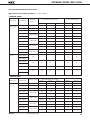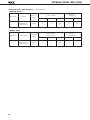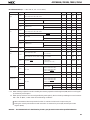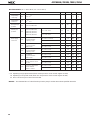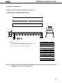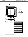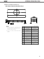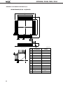
1
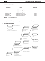
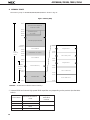
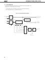
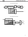
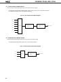
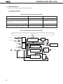
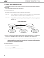
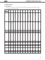
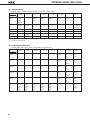
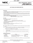
DATA SHEET MOS INTEGRATED CIRCUIT µPD78011B, 78012B, 78013, 78014 8-BIT SINGLE-CHIP MICROCOMPUTER DESCRIPTION The µPD78011B/78012B/78013/78014 are the prodcts in the µPD78014 subseries within the 78K/0 Series. The µPD78011B/78012B/78013/78014 have 8-bit resolution A/D converter, timer, serial interface, interrupt control, and many other peripheral hardware functions. A one-time PROM or EPROM product µPD78P014 capable of operating in the same power supply voltage range as of the mask ROM product and other development tools are also provided. Functions are described in detail in the following User's Manual, which should be read when carring out design work. µPD78014, 78014Y Series User's Manual: IEU-1343 FEATURES • Large on-chip ROM & RAM Item Product Name • • • • • • • Data Memory Program Memory (ROM) µPD78011B 8K bytes µPD78012B 16K bytes µPD78013 24K bytes µPD78014 32K bytes Package Internal HighSpeed RAM Buffer RAM 512 bytes 32 bytes • 64-pin plastic shrink DIP (750 mil) • 64-pin plastic QFP (■ ■ 14 mm) 1024bytes External memory expansion space : 64K bytes Instruction execution time can be varied from high-speed (0.4 µs) to ultra-low-speed (122 µs) I/O ports: 53 (N-ch open-drain : 4) 8-bit resolution A/D converter : 8 channels Serial interface : 2 channels Timer : 5 channels Operating voltage range : 2.7 to 6.0 V Application Telephone, VCR, audio, camera, home appliances, etc. The information in this document is subject to change without notice. Document No. IC-3179D (O.D.No. IC-8201F) Date Published January 1995 P Printed in Japan The mark ★ shows major revised points. © 1992 µPD78011B, 78012B, 78013, 78014 ORDERING INFORMATION Ordering Code Package µPD78011BCW-××× µPD78011BGC-×××-AB8 µPD78012BCW-××× µPD78012GC-×××-AB8 µPD78013CW-××× µPD78013GC-×××-AB8 µPD78014CW-××× µPD78014GC-×××-AB8 Remarks 64-pin 64-pin 64-pin 64-pin 64-pin 64-pin 64-pin 64-pin plastic plastic plastic plastic plastic plastic plastic plastic Quality Grade shrink DIP (750 QFP (■ ■ 14 mm) shrink DIP (750 QFP (■ ■ 14 mm) shrink DIP (750 QFP (■ ■ 14 mm) shrink DIP (750 QFP (■ ■ 14 mm) mil) Standard Standard Standard Standard Standard Standard Standard Standard mil) mil) mil) ××× indicates ROM code No. Please refer to "Quality grade on NEC Semiconductor Devices" (Document number IEI-1209) published by NEC Corporation to know the specification of quality grade on the devices and its recommended applications. ★ 78K/0 SERIES DEVELOPMENT µ PD78078Y SubSeries Products in Volume Production µ PD78078 SubSeries µ PD78064Y SubSeries Products under Development Y series products are compatible with I2C bus. µ PD78064 SubSeries 100-pin package LCD controller/driver, UART added 16-bit timer/event counter function enhanced 100-pin package 8-bit timer/event counter added External expansion function enhanced µ PD78054Y SubSeries µ PD78054 SubSeries 80-pin package UART, D/A converter, Real-time output port added 16-bit timer/event counter function enhanced µ PD78018FY SubSeries µ PD78014Y SubSeries µ PD78014 SubSeries µ PD78018F SubSeries 64-pin package Low-voltage, high-speed operation possible 64-pin package A/D converter, 16 bit-timer/event counter function, SIO with automatic transmit/receive function added Multiplication/division instruction added µ PD78044A SubSeries µ PD78044 SubSeries µ PD78024 SubSeries µ PD78002Y SubSeries µ PD78002 SubSeries 64-pin package 2 64-pin package A/D converter, 16 bit-timer/event counter, FIB controller/driver, Multiplication/division instruction added 80-pin package Automatic transmit/receive function added 6-bit up/down counter added FIP controller/driver function enhanced µ PD78098 SubSeries 80-pin package IEBus controller added µ PD78083 SubSeries 42/44-pin package UART, A/D converter, 8-bit timer/event counter function enhanced µ PD780208 SubSeries 100-pin package FIP controller/driver function enhanced µPD78011B, 78012B, 78013, 78014 OVERVIEW OF FUNCTION (1/2) µPD78011B Item µPD78012B µPD78013 µPD78014 16K bytes 24K bytes 32K bytes Product Name ROM Internal highspeed RAM Buffer RAM Internal memory 8K bytes 512 bytes 1024 bytes 32 bytes Memory space 64K bytes General registers 8 bits × 32 registers (8 bits × 8 registers × 4 banks) Instruction cycle On-chip instruction execution time cycle modification function When main system clock selected When subsystem clock selected 0.4 µs/0.8 µs/1.6 µs/3.2 µs/6.4 µs (at 10.0 MHz operation) 122 µs (at 32.768 kHz operation) Instruction set • • • • 16-bit operation Multiplication/division (8 bits × 8 bits,16 bits ÷ 8 bits) Bit manipulation (set, reset, test, boolean operation) BCD correction, etc. I/O ports Total • CMOS input • CMOS I/O • N-channel open-drain I/O (15 V withstand voltage) : 53 : 02 : 47 : 04 A/D converter • 8-bit resolution × 8 channels • Operable over a wide power supply voltage range: VDD = 2.7 to 6.0 V Serial interface • 3-wire/SBI/2-wire mode selectable: 1 channel • 3-wire mode (on-chip max. 32 bytes automatic data transmit/receive function): 1 channel Timer • • • • Timer output 3 (14-bit PWM output × 1) Clock output 39.1 kHz, 78.1 kHz, 156 kHz, 313 kHz, 625 kHz, 1.25 MHz (at main system clock 10.0 MHz operation), 32.768 kHz (at subsystem clock 32.768 kHz operation) Buzzer output 2.4 kHz, 4.9 kHz, 9.8 kHz (at main system clock 10.0 MHz operation) Vectored interrupts 16-bit timer/event counter : 8-bit timer/event counter : Watch timer : Watchdog timer : Maskable interrupts Internal : 8 External: 4 Non-maskable interrupt Internal : 1 Software interrupt Internal : 1 1 2 1 1 channel channels channel channel 3 µPD78011B, 78012B, 78013, 78014 OVERVIEW OF FUNCTION (2/2) Item Product Name Test input Internal : 1 External : 1 Operating voltage range VDD = 2.7 to 6.0 V Operating temperature range –40 to +85°C Package 4 µPD78011B µPD78012B • 64-pin plastic shrink DIP (750 mil) • 64-pin plastic QFP (■ ■ 14 mm) µPD78013 µPD78014 µPD78011B, 78012B, 78013, 78014 CONTENTS 1. PIN CONFIGURATION (TOP VIEW) ........................................................................................................ 6 2. BLOCK DIAGRAM .................................................................................................................................... 9 3. PIN FUNCTIONS ...................................................................................................................................... 10 3.1 PORT PINS ......................................................................................................................................................... 10 3.2 OTHER PORTS ................................................................................................................................................... 11 3.3 PIN I/O CIRCUIT AND RECOMMENDED CONNECTION OF UNUSED PINS ................................................ 13 4. MEMORY SPACE ..................................................................................................................................... 16 5. PERIPHEL HARDWARE FUNCTION FEATURES ................................................................................... 17 5.1 5.2 5.3 5.4 5.5 5.6 5.7 6. PORTS ................................................................................................................................................................ CLOCK GENERATOR ........................................................................................................................................ TIMER/EVENT COUNTER ................................................................................................................................ CLOCK OUTPUT CONTROL CIRCUIT .............................................................................................................. BUZZER OUTPUT CONTROL CIRCUIT ............................................................................................................ A/D CONVERTOR ............................................................................................................................................. SERIAL INTERFACES ........................................................................................................................................ 17 18 19 22 22 23 24 INTERRUPT FUNCTIONS AND TEST FUNCTIONS ............................................................................... 26 6.1 INTERRUPT FUNCTIONS ................................................................................................................................. 26 6.2 TEST FUNCTIONS ............................................................................................................................................. 29 7. EXTERNAL DEVICE EXPANTION FUNCTIONS ..................................................................................... 30 8. STANDBY FUNCTIONS ........................................................................................................................... 30 9. RESET FUNCTIONS ................................................................................................................................. 30 10. INSTRUCTION SET .................................................................................................................................. 31 11. ELECTRICAL SPECIFICATIONS .............................................................................................................. 34 12. CHARACTERISTIC CURVE (REFERENCE VALUES) .............................................................................. 58 13. PACKAGE INFORMATION ...................................................................................................................... 63 14. RECOMMENDED SOLDERING CONDITIONS ...................................................................................... 67 APPENDIX A. DEVELOPMENT TOOLS .......................................................................................................... 69 APPENDIX B. RELATED DOCUMENTS ......................................................................................................... 71 5 µPD78011B, 78012B, 78013, 78014 1. PIN CONFIGURATION (Top View) 64-Pin Plastic Shrink DIP (750 mil) 64 AV REF 2 63 AV DD P22/SCK1 3 62 P17/ANI7 P23/STB 4 61 P16/ANI6 P24/BUSY 5 60 P15/ANI5 P25/SI0/SB0 6 59 P14/ANI4 P26/SO0/SB1 7 58 P13/ANI3 P27/SCK0 8 57 P12/ANI2 P30/TO0 9 56 P11/ANI1 55 P10/ANI0 54 AV SS 53 P04/XT1 52 XT2 51 IC 50 X1 49 X2 48 V DD 47 P03/INTP3 46 P02/INTP2 45 P01/INTP1 44 P00/INTP0/TI0 43 RESET P31/TO1 10 P32/TO2 11 P33/TI1 12 P34/TI2 13 P35/PCL 14 P36/BUZ 15 P37 16 µPD78012BCW– × × × µPD78014CW– × × × 6 1 µPD78011BCW– × × ×, µPD78013CW– × × ×, Caution P20/SI1 P21/SO1 V SS 17 P40/AD0 18 P41/AD1 19 P42/AD2 20 P43/AD3 21 P44/AD4 22 P45/AD5 23 42 P67/ASTB P46/AD6 24 41 P66/WAIT P47/AD7 25 40 P65/WR P50/A8 26 39 P64/RD P51/A9 27 38 P63 P52/A10 28 37 P62 P53/A11 29 36 P61 P54/A12 30 35 P60 P55/A13 31 34 P57/A15 V SS 32 33 P56/A14 1. Always connect the IC (Internally Connected) pin to VSS directly. 2. Always connect the AVDD pin to VDD. 3. Always connect the AVSS pin to VSS. µPD78011B, 78012B, 78013, 78014 P27/SCK0 P26/SO0/SB1 P25/SI0/SB0 P24/BUSY P23/STB P22/SCK1 P21/SO1 P20/SI1 AV REF AV DD P17/ANI7 P16/ANI6 P15/ANI5 P14/ANI4 P13/ANI3 P12/ANI2 64-Pin Plastic QFP (■ ■ 14 mm) 64 63 62 61 60 59 58 57 56 55 54 53 52 51 50 49 48 1 P11/ANI1 P31/TO1 2 47 P10/ANI0 P32/TO2 3 46 AV SS P33/TI1 4 45 P04/XT1 P34/TI2 5 44 XT2 P35/PCL 6 43 IC P36/BUZ 7 42 X1 P37 8 41 X2 V SS 9 40 V DD 39 P03/INTP3 38 P02/INTP2 37 P01/INTP1 µPD78011BGC– × × × –AB8 µPD78012BGC– × × × –AB8 µPD78013GC– × × × –AB8 µPD78014GC– × × × –AB8 P30/TO0 34 P67/ASTB 16 17 P66/WAIT Caution 18 19 20 21 22 23 24 25 26 27 28 29 30 31 33 32 P65/WR 15 P46/AD6 P64/RD P45/AD5 P63 RESET P62 35 P61 14 P60 P44/AD4 P57/A15 P00/INTP0/TI0 P56/A14 36 V SS 13 P55/A13 P43/AD3 P54/A12 12 P53/A11 P42/AD2 P52/A10 11 P51/A9 P41/AD1 P50/A8 10 P47/AD7 P40/AD0 1. Always connect the IC (Internally Connected) pin to VSS directly. 2. Always connect the AVDD pin to VDD. 3. Always connect the AVSS pin to VSS. 7 µPD78011B, 78012B, 78013, 78014 P00 to P04 P10 to P17 P20 to P27 : Port 0 : Port 1 : Port 2 P30 to P37 P40 to P47 : Port 3 : Port 4 P50 to P57 P60 to P67 : Port 5 : Port 6 INTP0 to INTP3 : Interrupt From Peripherals TI0 to TI2 : Timer Input 8 TO0 to TO2 SB0, SB1 : Timer Output : Serial Bus SI0, SI1 SO0, SO1 : Serial Input : Serial Output SCK0, SCK1 PCL : Serial Clock : Programmable Clock BUZ STB : Buzzer Clock : Strobe BUSY : Busy AD0 to AD7 A8 to A15 : Address/Data Bus : Address Bus RD WR : Read Strobe : Write Strobe WAIT ASTB : Wait : Address Strobe X1, X2 XT1, XT2 : Crystal (Main System Clock) : Crystal (Subsystem Clock) RESET ANI0 to ANI7 : Reset : Analog Input AVDD AVSS : Analog Power Supply : Analog Ground AVREF VDD : Analog Reference Voltage : Power Supply VSS IC : Ground : Internally Connected TI0/INTP0/P00 TO1/P31 TI1/P33 TO2/P32 TI2/P34 16-bit TIMER/ EVENT COUNTER PROGRAM COUNTER 8-bit TIMER/ EVENT COUNTER 1 P00 P01-P03 P04 PORT1 P10-P17 PORT2 P20-P27 PORT3 P30-P37 PORT4 P40-P47 PORT5 P50-P57 PORT6 P60-P67 GENERAL REG. ROM PROGRAM MEMORY 8-bit TIMER/ EVENT COUNTER 2 PORT0 2. BLOCK DIAGRAM TO0/P30 DECODE AND CONTROL RAM DATA MEMORY WATCHDOG TIMER WATCH TIMER SI0/SB0/P25 SO0/SB1/P26 SCK0/P27 SERIAL INTERFACE 0 ALU PSW SP SO1/P21 SCK1/P22 STB/P23 SERIAL INTERFACE 1 BUSY/P24 ANI0/P10 -ANI7/P17 AVDD AVSS AVREF INTP0/P00 -INTP3/P03 BUZZER OUTPUT CLOCK OUTPUT CONTROL CLOCK DIVIDER CLOCK GENERATOR SUB MAIN AD0/P40AD7/P47 STAND BY CONTROL A8/P50A15/P57 A/D CONVERTER BUZ/P36 PCL/P35 P04/XT1 XT2 EXTERNAL ACCESS X1 X2 RD/P64 WR/P65 WAIT/P66 ASTB/P67 RESET VDD INTERRUPT CONTROL Remarks VSS IC Internal ROM & RAM capacity varies depending on the product. 9 µPD78011B, 78012B, 78013, 78014 SI1/P20 µPD78011B, 78012B, 78013, 78014 3. PIN FUNCTIONS 3.1 PORT PINS (1/2) Pin Name Input P00 Input/ output P01 P02 Function I/O Port 0 5-bit I/O port After Reset DualFunction Pin Input only Input INTP0/TI0 Input/output can be specified bit-wise. When used as an input port, pull-up resistor can be used by software. Input INTP1 INTP2 P03 INTP3 P04*1 Input Input only P10 to P17 Input/ output Port 1 8-bit input/output port. Input/output can be specified bit-wise. When used as an input port, pull-up resistor can be used by software.*2 P20 Input/ output Port 2 8-bit input/output port. Input/output can be specified bit-wise. When used as an input port, pull-up resistor can be used by software. P21 P22 P23 Input XT1 Input ANI0 to ANI7 Input SI1 SO1 SCK1 STB P24 BUSY P25 SI0/SB0 P26 SO0/SB1 P27 SCK0 Input/ output P30 P31 P32 P33 Port 3 8-bit input/output port. Input/output can be specified in 1-bit units. When used as an input port, pull-up resistor can be used by software. Input TO0 TO1 TO2 TI1 P34 TI2 P35 PCL P36 BUZ P37 — P40 to P47 * 1. 2. 10 Input/ output Port 4 8-bit input/output port. Input/output can be specified in 8-bit unit. When used as an input port, pull-up resistor can be used by software. Test input flag (KRIF) is set to 1 by falling edge detection. Input AD0 to AD7 When using the P04/XT1 pins as an input port, set 1 to bit 6 (REC) of the processor control register. Do not use the on-chip feedback register of the subsystem clock oscillator. When using the P10/ANI0 to P17/ANI7 pins as the A/D converter analog input, pull-up resistor is automatically unused. µPD78011B, 78012B, 78013, 78014 3.1 PORT PINS (2/2) Function Pin Name I/O P50 to P57 Input/ output Port 5 8-bit input/output port. LED can be driven directly. Input/output can be specified bit-wise. When used as an input port, pull-up resistor can be used by software. P60 Input/ output Port 6 8-bit input/output port. Input/output can be specified bit-wise. P61 P62 P63 After Reset Input A8 to A15 N-ch open-drain input/output port. Input On-chip pull-up resistor can be specified by mask option. LED can be driven directly. P64 RD When used as an input port, pull-up resistor can be used by software. P65 DualFunction Pin WR P66 WAIT P67 ASTB Caution When pull-up resistors are not used (specified by mask option), the low-level input leak current increases with -200 µA (MAX.) under either of the following conditions. 1 When the external device expansion function is used and a low-level is input to the pin. 2 During the 3-clock period when a read instruction is executed on port 6 (P6) and the port mode register (PM6). 3.2 OTHER PORTS (1/2) Pin Name INTP0 I/O Input INTP1 INTP2 INTP3 SI0 Function External interrupt input by which the effective edge (rising edge, falling edge, or both rising edge and falling edge) can be specified. After Reset Input Serial interface serial data input. P02 P03 Input Output Serial interface serial data output. Input SO1 SB0 P25/SB0 P20 SI1 SO0 P00/TI0 P01 Falling edge detection external interrupt input. Input DualFunction Pin P26/SB1 P21 Input Input /output Serial interface serial data input/output. Input /output Serial interface serial clock input/output. STB Output Serial interface automatic transmit/receive strobe output. Input P23 BUSY Input Serial interface automatic transmit/receive busy input. Input P24 SB1 SCK0 SCK1 P25/SI0 P26/SO0 Input P27 P22 11 µPD78011B, 78012B, 78013, 78014 3.2 OTHER PORTS (2/2) Pin Name TI0 I/O Input Function External count clock input to 16-bit timer (TM0). TI1 External count clock input to 8-bit timer (TM1). TI2 External count clock input to 8-bit timer (TM2). TO0 Output 16-bit timer output (shared as 14-bit PWM output). After Reset DualFunction Pin Input P00/INTP0 P33 P34 Input 8-bit timer output. TO1 P31 TO2 PCL BUZ P30 P32 Output Output Clock output (for main system clock, subsystem clock trimming). Input P35 Buzzer output. Input P36 P40 to P47 AD0 to AD7 Input /output Low-order address/data bus at external memory expansion. Input A8 to A15 Output High-order address bus at external memory expansion. Input P50 to P57 RD Output External memory read operation strobe signal output. Input P64 WR External memory write operation strobe signal output. P65 Input Wait insertion at external memory access. Input P66 ASTB Output Strobe output which latches the address information output at port 4 and port 5 to access external memory. Input P67 ANI0 to ANI7 Input A/D converter analog input. Input P10 to P17 AVREF Input A/D converter reference voltage input. — — AVDD — A/D converter analog power supply. Connected to VDD. — — AVSS — A/D converter ground potential. Connected to VSS. — — RESET Input System reset input. — — X1 Input Main system clock oscillation crystal connection. — — X2 — — — XT1 Input Input P04 XT2 — — — VDD — Positive power supply. — — VSS — Ground potential. — — IC — Internal connection. Connected to VSS directly. — — WAIT 12 Subsystem clock oscillation crystal connection. µPD78011B, 78012B, 78013, 78014 3.3 PIN I/O CIRCUITS AND RECOMMENDED CONNECTION OF UNUSED PINS The input/output circuit type of each pin and recommended connection of unused pins are shown in Table 31. For the input/output circuit configuration of each type, see Fig. 3-1. Table 3-1 Input/Output Circuit Type of Each Pin (1/2) Pin Name P00/INTP0/TI0 P01/INTP1 Input/output Circuit Type I/O Recommended Connection when Not Used 2 Input Connected to VSS . 8-A Input/output Input : Connected to VSS . Output : Leave open. P02/INTP2 P03/INTP3 16 Input Connected to VSS . P10/ANI0 to P17/ANI7 11 Input/output Input Output : Connected to VDD or VSS . : Leave open. P20/SI1 8-A Input/output P21/SO1 5-A Input Output : Connected to VDD or VSS . : Leave open. P22/SCK1 8-A P23/STB 5-A P24/BUSY 8-A P25/SI0/SB0 10-A Input/output Input Output : Connected to VDD or VSS . : Leave open. P04/XT1 P26/SO0/SB1 P27/SCK0 P30/TO0 5-A P31/TO1 P32/TO2 P33/TI1 8-A P34/TI2 P35/PCL 5-A P36/BUZ P37 P40/AD0 to P47/AD7 5-E Input/output Input Output : Connected to VDD or VSS . : Leave open. P50/A8 to P57/A15 5-A Input/output P60 to P63 13-B Input Output : Connected to VDD or VSS . : Leave open. P64/RD 5-A P65/WR P66/WAIT P67/ASTB 13 µPD78011B, 78012B, 78013, 78014 Table 3-1 Input/Output Circuit Type of Each Pin (2/2) Input/Output Circuit Type Pin Name RESET 2 XT2 16 AVREF — Recommended Connection when Not Used I/O Input — — Leave open. Connected to VSS . AVDD Connected to VDD . AVSS Connected to VSS . IC Connected to VSS directly. 14 µPD78011B, 78012B, 78013, 78014 Fig. 3-1 Pin Input/Output Circuits Type 10-A Type 2 V DD pullup enable P-ch IN V DD data P-ch IN / OUT Schmitt-Triggered Input with Hysteresis Characteristic Type 5-A V DD IN / OUT P-ch N-ch N-ch P-ch + – input enable Type 5-E Type 13-B V DD data output disable Comparator N-ch V REF (Threshold Voltage) input enable pullup enable P-ch V DD P-ch data IN / OUT output disable V DD pullup enable P-ch data N-ch Type 11 V DD pullup enable open drain output disable V DD Mask Option P-ch V DD data output disable N-ch P-ch V DD IN / OUT output disable IN / OUT N-ch P-ch RD Middle-High Voltage Input Buffer V DD Type 8-A pullup enable Type 16 feedback cut-off P-ch P-ch V DD data P-ch IN / OUT output disable N-ch XT1 XT2 15 µPD78011B, 78012B, 78013, 78014 4. MEMORY SPACE The memory map of µPD78011B/78012B/78013/78014 is shown in Fig 4-1. Fig.4-1 Memory Map FFFFH Special Function Registers (SFR) 256 × 8 Bits FF00H FEFFH FEE0H FEDFH General Registers 32 × 8 Bits Internal High-Speed RAM* mmmmH mmmmH–1 nnnnH Use Prohibited FAE0H FADFH Data Memory Space FAC0H FABFH Program Area 1000H 0FFFH Buffer RAM 32 × 8 Bits CALLF Entry Area Use Prohibited 0800H 07FFH FA80H FA7FH Program Area Program Memory Space nnnnH+1 nnnnH 0080H 007FH External Memory CALLT Table Area 0040H 003FH Internal ROM* Vector Table Area 0000H 0000H Remarks Shaded area indicates internal memory. * Intermal ROM and internal high-speed RAM capacities vary depending on the product (see the table below). Product Name 16 Intenal ROM End Address nnnnH µPD78011B 1FFFH µPD78012B 3FFFH µPD78013 5FFFH µPD78014 7FFFH Internal High-Speed RAM StartAddress mmmmH FD00H FB00H µPD78011B, 78012B, 78013, 78014 5 PERIPHERAL HARDWARE FUNCTION FEATURES 5.1 PORTS The I/O port has the following three types • CMOS input (P00, P04) • CMOS input/output (P01 to P03, port 1 to port 5, P64 to P67) : 2 : 47 • N-ch open-drain input/output(15V withstand voltage) (P60 to P63) : Total 4 : 53 Table 5-1 Functions of Ports Port Name Port 0 Pin Name P00, P04 Dedicated Input port P01 to P03 Input/output ports. Input/output can be specified bit-wise. Port 1 P10 to P17 Port 2 P20 to P27 Port 3 P30 to P37 Port 4 P40 to P47 Port 5 P50 to P57 Port 6 P60 to P63 P64 to P67 Caution Function When used as an input port, pull-up resistor can be used by software. Input/output ports. Input/output can be specified bit-wise. When used as an input port, pull-up resistor can be used by software. Input/output ports. Input/output can be specified bit-wise. When used as an input port, pull-up resistor can be used by software. Input/output ports. Input/output can be specified bit-wise. When used as an input port, pull-up resistor can be used by software. Input/output ports. Input/output can be specified in 8-bit units. When used as an input port, pull-up resistor can be used by software. Test input flag (KRIF) is set to 1 by falling edge detection. Input/output ports. Input/output can be specified bit-wise. When used as an input port, pull-up resistor can be used by software. LED can be driven directly. N-ch open-drain input/output port. Input/output can be specified bit-wise. On-chip pull-up resistor can be specified by mask option. LED can be driven directly. Input/output ports. Input/output can be specified bit-wise. When used as an input port, pull-up resistor can be used by software. When pull-up resistors are not used (specified by mask option), low-level input leak current increases with – 200 mA (MAX.) under either of the following conditions. 1 When the external device expansion function is used and a low-level is input to the pin. 2 During the 3-clock period when a read instruction is executed on port 6 (P6) and the port mode register (PM6). 17 µPD78011B, 78012B, 78013, 78014 5.2 CLOCK GENERATOR There are two types of clock generator: main system clock and subsystem clock. The instruction exection time can be changed. • 0.4µs/0.8µs/1.6µs/3.2µs/6.4µs (Main system clock: at 10.0 MHz operation) • 122µs (Subsystem clock: at 32.768 KHz operation) Fig. 5-1 Clock Generator Block Diagram XT1/P04 XT2 Subsystem Clock Osicillator Watch Timer Clock Output Function fXT Prescaler X1 X2 Main System Clock Osicillator fX Clock to Peripheral Hardware Prescaler fX fX fX fX 2 22 23 24 STOP Selector Standby Control Circuit Wait Control Circuit INTP0 Sampling Clock 18 CPU Clock (fCPU) µPD78011B, 78012B, 78013, 78014 5.3 TIMER/EVENT COUNTER The following five channels are incorporated in the timer/event counter. • 16-bit timer/event counter : 1 channel • 8-bit timer/event counter • Watch timer : 2 channels : 1 channel • Watchdog timer : 1 channel Table 5-2 Types and Features of Timer/Event Counter Type Functions 16-bit Timer/Event Counter 8-bit Timer/Event Counter Interval timer 1 channel 2 channels 1channel 1 channel Externanal event counter 1 channel 2 channels – – Timer output 1 output 2 outputs – – PWM output 1 output – – – 1 input – – – 1 output 2 outputs – – 2 2 2 1 Pulse width mesurement Sqare wave output Interrupt request Watch Timer Watchdog Timer 19 µPD78011B, 78012B, 78013, 78014 Fig. 5-2 16-bit Timer/Enent Counter Block Diagram Internal Bus 16-Bit Compare Register (CR00) INTTM0 PWM Pulse Output Control Circuit Match fX/2 fX/22 fX/23 TI0/INTP0/P00 Output Control Circuit TO0/P30 16-Bit Timer Register (TM0) Selector Edge Detection Circuit Selector Clear INTP0 16-Bit Capture Register (CR01) Internal Bus Fig. 5-3 8-bit Timer/Enent Counter Block Diagram Internal Bus INTIM1 8-Bit Compare Register (CR10) 8-Bit Compare Register (CR20) Selector Match Output Control Circuit INTTM2 fX/22–fX/210 fX/212 TO2/P32 Selector TI1/P33 8-Bit Timer Register 1 (TM1) Clear Selector 8-Bit Timer Register 2 (TM2) Clear fX/22–fX/210 12 fX/2 Selector Selector TI2/P34 Output Control Circuit Internal Bus 20 TO1/P31 µPD78011B, 78012B, 78013, 78014 Fig. 5-4 Watch Timer Block Diagram Selector fX/28 5-Bit Counter fW 214 Selector Prescaler Selector fXT fW 24 fW 26 fW 25 fW 28 fW 27 INTWT fW 213 fW 29 Selector INTTM3 Fig. 5-5 Watchdog Timer Block Diagram fX 24 Prescaler fX 25 fX 26 fX 27 fX 28 fX 29 fX 210 fX 212 INTWDT Maskable Interrupt Request Selector 8-Bit Counter Control Circuit RESET INTWDT Non-Maskable Interrupt Request 21 µPD78011B, 78012B, 78013, 78014 5.4 CLOCK OUTPUT CONTROL CIRCUIT The clock with the following frequencies can be output for clock output. • 39.1 kHz/78.1 kHz/156 kHz/313 kHz/625 kHz/1.25 MHz (Main system clock: at 10.0 MHz operation) • 32.768 kHz (Subsystem clock: at 32.768 kHz operation) Fig. 5-6 Clock Output Control Block Diagram fX/23 fX/24 fX/25 fX/26 Selector Synchronization Circuit Output Control Circuit fX/27 fX/28 fXT 5.5 BUZZER OUTPUT CONTROL CIRCUIT The clock with the following frequencies can be output for buzzer output. • 2.4 kHz/4.9 kHz/9.8 kHz (Main system clock: at 10.0 MHz operation) Fig. 5-7 Buzzer Output Control Block Diagram fX/210 fX/211 fX/212 22 Selector Output Control Circuit BUZ/P36 PCL/P35 µPD78011B, 78012B, 78013, 78014 5.6 A/D CONVERTER The A/D converter has on-chip eight 8-bit resolution channels. There are the following two method to start A/D conversion. • Hardware starting • Software starting Fig. 5-8 A/D Converter Block Diagram Series Resistor String AVDD Sample & Hold Circuit ANI0/P10 AVREF ANI1/P11 Voltage Comparator ANI2/P12 ANI3/P13 Tap Selector Selector ANI4/P14 ANI5/P15 ANI6/P16 Succesive Approxmation Register (SAR) ANI7/P17 INTP3/P03 Falling Edge Detector Control Circuit AVSS INTAD INTP3 A/D Conversion Result Register (ADCR) Internal Bus 23 µPD78011B, 78012B, 78013, 78014 5.7 SERIAL INTERFACES There are two on-chip clocked serial interfaces as follows. • Serial Interface channel 0 • Serial Interface channel 1 Table 5-3 Type and Function of Serial Interface Function Serial Interface Channel 0 Serial Interface Channel 1 3-wire serial I/O mode ● (MSB/LSB-first switchable) ● (MSB/LSB-first switchable) 3-wire serial I/O mode with automatic data transmit – ● (MSB/LSB-first switchable) SBI (Serial Bus Interface) mode ● (MSB-first) – 2-wire serial I/O mode● (MSB-first) – – /receive function Fig. 5-9 Serial Interface Channel 0 Block Diagram Internal Bus SI0/SB0/P25 Selector SO0/SB1/P26 Selector SCK0/P27 Serial I/O Shift Register 0 (SIO0) Bus Release/Command/ Acknowledge Detection Circuit Serial Counter Output Latch Busy/Acknowlede Output Circuit Interrupt Request Signal Generator INTCSI0 fx/22–fx/29 Serial Clock Control Circuit 24 Selector TO2 µPD78011B, 78012B, 78013, 78014 Fig. 5-10 Serial Interface Channel 1 Block Diagram Internal Bus Automatic Data Transmit/ Receive Address Pointer (ADTP) SI1/P20 Buffer RAM Serial I/O Shift Register 1 (SIO0) SO1/P21 STB/P23 BUSY/P24 SCK/P22 Handshake Control Circuit Serial Counter Interrupt Request Signal Generator INTCSI1 fX/22 – fX/29 Serial Clock Control Circuit Selector TO2 25 µPD78011B, 78012B, 78013, 78014 6. INTERRUPT FUNCTIONS AND TEST FUNCTIONS 6.1 INTERRUPT FUNCTIONS There are the 14 interrupt functions of 3 different kind as shown below. • Non-maskable interrupt • Maskable interrupt : 1 : 12 • Software interrupt : 1 Table 6-1 Interrupt Source List Interrupt Source Interrupt Type Default Priority*1 Name Trigger Non-maskable ––– INTWDT Watchdog timer overflow (with nonmaskable interrupt selected) Maskable 0 INTWDT Watchdog timer overflow (with interval Internal /External Vector Table Address Basic*2 Configuratin Type Internal 0004H A B timer selected) Software * 1 INTP0 2 Pin input edge detection 0006H C INTP1 0008H D 3 INTP2 000AH 4 INTP3 000CH 5 INTCSI0 Serial interface channel 0 transfer end 6 INTCSI1 Serial interface channel 1 transfer end 0010H 7 INTTM3 Reference time interval signal from watch timer 0012H 8 INTTM0 16 bit timer/event counter match signal generation 0014H 9 INTTM1 8-bit timer/event counter 1 match signal generation 0016H 10 INTTM2 8-bit timer/event counter 2 match signal generation 0018H 11 INTAD A/D converter conversion end 001AH ––– BRK BRK instruction execution External Internal Internal 003EH B E 1. The default pririty is the priority applicable when more than one maskable interrupt is generated. 0 is the highest priority and 11, the lowest. 2. Basic configuration types A to E correspond to A to E on the next page. 26 000EH µPD78011B, 78012B, 78013, 78014 Fig. 6-1 Basic Interrupt Function Configuration (1/2) (A) Internal Non-Maskable Interrupt Internal Bus Interrupt Request Vector Table Address Generator Priority Control Circuit Standby Release Signal (B) Internal Maskable Interrupt Internal Bus MK Interrupt Request PR IE ISP Vector Table Address Generator Priority Control Circuit IF Standby Release Signal (C) External Maskable Interrupt (INTP0) Internal Bus Sampling Clock Select Register (SCS) Interrupt Request Sampling Clock External Interrupt Mode Register (INTM0) Edge Detector MK IF IE PR Priority Control Circuit ISP Vector Table Address Generator Standby Release Signal 27 µPD78011B, 78012B, 78013, 78014 Fig. 6-1 Basic Interrupt Function Configuration (2/2) (D) External Maskable Interrupt (Except INTP0) Internal Bus External Interrupt Mode Register (INTM0) Interrupt Request Edge Detector MK IE PR Priority Control Circuit IF ISP Vector Table Address Generator Standby Release Signal (E) Software Interrupt Internal Bus Interrupt Request Remarks 28 1. 2. 3. 4. 5. IF IE ISP MK PR : Interrupt request flag : Interrupt enable flag : In-service priority flag : Interrupt mask flag : Priority spcification flag Priority Control Circuit Vector Table Address Generator µPD78011B, 78012B, 78013, 78014 6.2 TEST FUNCTIONS There are two test functions as shown in Table 6-2. Table 6-2 Test Source List Test Source Internal/External Name Trigger INTWT Watch timer overflow Internal INTPT4 Port 4 falling edge detection External Fig. 6-2 Test Function Basic Configuration Internal Bus MK Test Input Remarks 1. IF 2. MK : Test mask flag IF Standby Release Signal : Test input flag 29 µPD78011B, 78012B, 78013, 78014 7. EXTERNAL DEVICE EXPANSION FUNCTIONS The external device expansion function is used to connect external devices to areas other than the internal ROM, RAM and SFR. Ports 4 to 6 are used for connection with external devices. 8. STANDBY FUNCTIONS There are the following two standby functions to reduce the current dissipation. • HALT mode : The CPU operating clock is stopped. The average consumption current can be reduced by intermittent operation in combination with the normal operat ing mode. • STOP mode : The main system clock oscillation is stopped. The whole operation by the main system clock is stopped, so that the system operates withultra-low power consumption using only the subsystem clock. Fig. 8-1 Standby Functions CSS=1 Main System Clock Operation Interrupt Request CSS=0 HALT Instruction STOP Instruction Interrupt Request STOP Mode (Main system clock oscillation stopped) * HALT Mode (Clock supply to CPU is stopped, oscillation) Subsystem Clock Operation* Interrupt Request HALT Instruction HALT Mode* (Clock supply to CPU is stopped, oscillation) The power consumption can be reduced by stopping the main system clock. When the CPU is operating on the subsystem clock, set the MCC to stop the main system clock. The STOP instruction cannot be used. Caution When the main system clock is stopped and the system is operated by the subsystem clock, the subsystem clock should be switched again to the main system clock after the oscillation stabilization time is secured by the program by the program. 9. RESET FUNCTIONS There are the following two reset methods. • External reset input by RESET pin. • Internal reset by watchdog timer runaway time detection. 30 µPD78011B, 78012B, 78013, 78014 10. INSTRUCTION SET (1) 8-Bit Instruction MOV, XCH, ADD, ADDC, SUB, SUBC, AND, OR, XOR, CMP, MULU, DIVUW, INC, DEC, ROR, ROL, RORC, ROLC, ROR4, ROL4, PUSH, POP, DBNZ 2nd Operand [HL+byte] #byte A r* sfr saddr !addr16 PSW [DE] [HL] 1st Operand A r [HL+B] $adder16 1 None [HL+C] ADD MOV MOV MOV MOV ADDC XCH XCH XCH XCH MOV MOV MOV MOV ROR XCH XCH XCH ROL SUB ADD ADD ADD ADD ADD RORC SUBC ADDC ADDC ADDC ADDC ADDC ROLC AND SUB SUB SUB SUB SUB OR SUBC SUBC SUBC SUBC SUBC XOR AND AND AND AND AND CMP OR OR OR OR OR MOV XOR XOR XOR XOR XOR CMP CMP CMP CMP CMP MOV INC ADD DEC ADDC SUB SUBC AND OR XOR CMP r1 DBNZ sfr sadder MOV MOV MOV MOV ADD DBNZ INC DEC ADDC SUB SUBC AND OR XOR CMP !adder16 PSW MOV MOV MOV PUSH POP [DE] MOV [HL] MOV [HL+byte] MOV ROR4 ROL4 [HL+B] [HL+C] * X MULU C DIVUW Except r=A 31 µPD78011B, 78012B, 78013, 78014 (2) 16-Bit Instruction MOVW, XCHW ADDW, SUBW, CMPW, PUSH, POP, INCW, DECW 2nd Operand 1st Operand AX #byte AX rp* ADDW MOVW SUBW XCHW sfrp MOVW saddrp MOVW !addr16 MOVW SP None MOVW CMPW rp MOVW MOVW* INCW, DECW PUSH, POP sfrp MOVW MOVW sadderp MOVW MOVW MOVW MOVW !adder16 SP * MOVW Only when rp=BC, DE, HL. (3) Bit Manipulation Instruction MOV1, AND1, OR1, XOR1, SET1, CLR1, NOT1, BT, BF, BTCLR 2nd Operand A.bit sfr.bit saddr.bit PWS.bit [HL].bit CY $addr16 None 1st Operand A.bit MOV1 BT SET1 BF CLR1 BTCLR sfr.bit MOV1 BT SET1 BF CLR1 BTCLR saddr.bit MOV1 BT SET1 BF CLR1 BTCLR PSW.bit MOV1 BT SET1 BF CLR1 BTCLR [HL].bit MOV1 BT SET1 BF CLR1 BTCLR CY 32 MOV1 MOV1 MOV1 MOV1 MOV1 SET1 AND1 AND1 AND1 AND1 AND1 CLR1 NOT1 OR1 OR1 OR1 OR1 OR1 XOR1 XOR1 XOR1 XOR1 XOR1 µPD78011B, 78012B, 78013, 78014 (4) Call Instruction/Branch Instruction CALL, CALLF, CALLT, BR, BC, BNC, BZ, BNZ, BT, BF, BTCLR, DBNZ 2nd Operand AX !addr16 !addr11 [addr5] $addr16 1st Operand Basic instruction BR CALL, BR CALLF CALLT BR, BC, BNC, BZ, BNZ Compound instruction BT, BF, BTCLR, DBNZ (5) Other Instruction ADJBA, ADJBS, BRK, RET, RETI, RETB, SEL, NOP, EI, DI, HALT, STOP 33 µPD78011B, 78012B, 78013, 78014 11. ELECTRICAL SPECIFICATIONS Absolute Maximum Ratings (Ta = 25 °C) Parameter Symbol Supply voltage Test Conditions Rating Unit VDD –0.3 to + 7.0 V AVDD –0.3 to VDD + 0.3 V AVREF –0.3 to VDD + 0.3 V –0.3 to + 0.3 V –0.3 to VDD + 0.3 V –0.3 to +16 V –0.3 to VDD + 0.3 V AVSS –0.3 to AVREF + 0.3 V 1 pin –10 mA P10 to P17, P20 to P27, P30 to P37 total –15 mA P01 to P03, P40 to P47, P50 to P57, P60 to P67 total –15 mA Peak value 30 mA Effective value 15 mA Peak value 100 mA Effective value 70 mA P01 to P03, P56, P57, Peak value 100 mA P60 to P67 total Effective value 70 mA P01 to P03, Peak value 50 mA P64 to P67 total Effective value 20 mA P10 to P17, P20 to P27, P30 to P37 Peak value 50 mA total 20 mA AVSS Input voltage VI1 VI2 Output voltage Analog input voltage P40 toP47, P50 to P57, P64 to P67, X1, X2, XT2 P60 to P67 Open-drain VO VAN Output current high P00 to P04, P10 to P17, P20 to P27, P30 toP37 IOH P10 to P17 Output Analog input pin 1 pin current low P40 to P47, P50 to P55 total IOL* Effective value Operating temperature Topt –40 to +85 °C Storage temperature Tstg –65 to +150 °C * Effective value should be calculated as follows: [Effective value] = [Peak value] × √duty Caution Product quality may suffer if the absolute maximum rating is exceeded for even a single parameter or even momentarily. That is, the absolute maximuam ratings are rated values at which the product is on the verge of suffering physical damage, and therefore the product must be used under conditions which ensure that the absolute maximum ratings are not exceeded. 34 µPD78011B, 78012B, 78013, 78014 Capacitance ( Ta = 25 °C, VDD = VSS = 0 V ) Parameter Symbol Input capacitance CIN Test Conditions MIN. TYP. f=1 MHz Unmeasured pins returned to 0 V I/O capacitance MAX. Unit 15 pF 15 pF 20 pF P01 to P03, P10 to P17, f=1 MHz Unmeasured CIO pins returned to 0 V P20 to P27, P30 toP37, P40 toP47, P50 to P57, P64 to P67 P60 to P63 Remarks The characteristics of a dual-function pin and a port pin are the same unless specified otherwise. Main System Clock Oscillation Circuit Characteristics ( Ta = –40 to +85 °C, VDD = 2.7 to 6.0 V) Resonator Recommended Circuit Ceramic resonator X1 X2 VSS Parameter Test Conditions Oscillator VDD = Oscillator frequency (fX) *1 voltage range Oscillation After VDD reaches oscil- stabilization time *2 lator voltage range MIN. MIN. TYP. 1 MAX. Unit 10 MHz 4 ms 10 MHz R1 C1 C2 Crystal resonator X1 X2 VSS C1 C2 Oscillator 1 frequency (fX) *1 Oscillation 8.38 10 VDD = 4.5 to 6.0 V ms stabilization time *2 External clock X1 input X1 X2 30 1.0 10.0 MHz 42.5 500 ns frequency (fX) *1 X1 input µPD74HCU04 high/low level width (tXH , tXL) * 1. Indicates only oscillation circuit characteristics. Refer to “AC Characteristics” for instruction execution time. 2. Time required to stabilize oscillation after reset or STOP mode release. Caution 1. When using the main system clock oscillator, wirinin the area enclosed with the dotted line should be carried out as follows to avoid an adverse effect from wiring capacitance. ● Wiring should be as short as possible. ● Wiring should not cross other signal lines. ● Wiring should not be placed close to a varying high current. ● The potential of the oscillator capacitor groundshould be the same as VSS. ● Do not ground wiring to a ground pattern in which a high current flows. ● Do not fetch a signal from the oscillator. 2. When the main system clock is stopped and the system is operated by the subsystem clock, the subsystem clock should be switched again to the main system clock after the oscillation stabilization time is secured by the program. 35 µPD78011B, 78012B, 78013, 78014 Subsystem Clock Oscillation Circuit Characteristics (Ta = –40 to +85 °C, VDD = 2.7 to 6.0 V) Resonator Crystal Recommended Circuit XT1 XT2 VSS Parameter Test Conditions Oscillator MIN. TYP. MAX. Unit 32 32.768 35 kHz 1.2 2 frequency (fXT) *1 resonator R2 C3 C4 Oscillation VDD = 4.5 to 6.0 V stabilization time *2 XT1 input External clock s 10 XT1 XT2 frequency (fXT) *1 32 100 kHz 5 15 µs XT1 input high/low level width (tXTH , tXTL) * 1. Indicates only oscillation circuit characteristics. Refer to “AC Characteristics” for instruction execution time. 2. Time required to stabilize oscillation after VDD reaches oscillator voltage MIN. Caution 1. When using the subsystem clock oscillator, wiring in the area enclosed with the dotted line should be carried out as follows to avoid an adverse effect from wiring capacitance. ● Wiring should be as short as possible. ● Wiring should not cross other signal lines. ● Wiring should not be placed close to a varying high current. ● The potential of the oscillator capacitor ground should be the same as VSS. ● Do not ground wiring to a ground pattern in which a high current flows. ● Do not fetch a signal from the oscillator. 2. The subsystem clock oscillation circuit is a circuit with a low amplification level,more prone to misoperation due to noise than the main system clock. Particular care is therefore required with the wiring method when the subsystem clock is used. 36 µPD78011B, 78012B, 78013, 78014 Recommended Oscillation Circuit Constant Main system clock: Ceramic resonator (Ta = –40 to +85 °C) µPD78011B, 78012B Manufacture Product Name Frequency Recommended Circuit Constant C1 (pF) Murata Mfg. Co., Ltd. Oscillator Voltage Range (MHz) C2 (pF) R1 (kΩ) MIN. (V) MAX. (V) CSB1000J 1.00 100 100 6.8 2.9 6.0 CSB××××J 1.01 to 1.25 100 100 4.7 2.7 6.0 CSA×. ×××MK 1.26 to 1.79 100 100 0 2.7 6.0 100 100 0 2.7 6.0 Built-in Built-in 0 2.7 6.0 30 30 0 2.7 6.0 Built-in Built-in 0 2.7 6.0 30 30 0 2.7 6.0 Built-in Built-in 0 2.7 6.0 30 30 0 2.9 6.0 Built-in Built-in 0 2.9 6.0 4.19 – – – 2.7 6.0 4.19 33 33 – 2.7 6.0 10.0 33 33 – 2.8 6.0 1.00 100 100 2.2 2.7 6.0 CSA×. ××MG 1.80 to 2.44 CST×. ××MG CSA×. ××MG CST×. ××MGW 2.45 to 4.18 CSA×. ××MG CST×. ××MGW 4.19 to 6.00 CSA×. ××MT CST×. ××MTW Kyocera 6.01 to 10.0 KBR-4.19MWS KBR-4.19MKS KBR-4.19MSA PBRC4.19A KBR-10.0M KBR-1000F KBR-1000Y µPD78013, 78014 Oscillator Voltage Range Recommended Circuit Constant Manufacture Murata Mfg. Co., Ltd. Product Name Frequency (MHz) C1 (pF) C2 (pF) R1 (kΩ) MIN. (V) MAX. (V) CSB1000J 1.00 100 100 6.8 2.7 6.0 CSB××××J 1.01 to 1.25 100 100 4.7 2.7 6.0 CSA×. ×××MK 1.26 to 1.79 100 100 0 2.7 6.0 100 100 0 2.7 6.0 Built-in Built-in 0 2.7 6.0 30 30 0 2.7 6.0 Built-in Built-in 0 2.7 6.0 30 30 0 2.7 6.0 Built-in Built-in 0 2.7 6.0 30 30 0 2.7 6.0 Built-in Built-in 0 2.7 6.0 CSA×. ××MG CST×. ××MG 1.80 to 2.44 CSA×. ××MG CST×. ××MGW 2.45 to 4.18 CSA×. ××MG CST×. ××MGW 4.19 to 6.00 CSA×. ××MT 6.01 to 10.0 CST×. ××MTW Remarks ××××, ×. ×××, ×. ×× indicate frequency. 37 µPD78011B, 78012B, 78013, 78014 Subsystem clock: Cristal resonator (Ta = –40 to + 60 °C) µPD78011B, 78012B Frequency Manufacture Products Oscillator Circuit Constant Voltage Range (MHz) C3 (pF) Daishinku Recommended C4 (pF) R2 (kΩ) MIN. (V) MAX. (V) DT-38 (1TA632 E00, load capacitance 6.3 pF) 32.768 8 8 100 2.7 6.0 µPD78013, 78014 Frequency Manufacture Product Name Voltage Range C4 (pF) R2 (kΩ) MIN. (V) MAX. (V) DT-38 (1TA632 E00, load capacitance 6.3 pF) 38 Oscillator Circuit Constant (MHz) C3 (pF) Daishinku Recommended 32.768 12 12 100 2.7 6.0 µPD78011B, 78012B, 78013, 78014 DC Characteristics (Ta = –40 to +85 °C, VDD = 2.7 to 6.0 V) Parameter Input voltage high Symbol Test Conditions MIN. VDD V VIH2 P00 to P03, P20, P22, P24 to P27, P33, P34, RESET 0.8 VDD VDD V VIH3 P60 to P63 0.7 VDD 15 V VIH4 X1, X2 VDD-0.5 VDD V VDD-0.5 VDD V VIH5 XT1/P04, XT2 VDD-0.3 VDD V VIL1 P10 to P17, P21, P23, P30 to P32, P35 to P37 P40 to P47, P50 to P57, P64 to P67 0 0.3 VDD V P00 to P03, P20, P22, P24 to P27, P33, P34, RESET 0 0.2 VDD V 0 0.3 VDD V 0 0.2 VDD V 0 0.4 V VIL3 P60 to P63 VIL4 X1, X2 VIL5 XT1/P04, XT2 Output voltage VOH1 Output voltage low Open-drain VDD = 4.5 to 6.0 V V V V IOH = –100 µA VDD-0.5 V P01 to P03, P10 to P17, P20 to P27 P30 to P37, P40 to P47, P64 to P67 VDD = 4.5 to 6.0 V, IOL = 1.6 mA VOL2 SB0, SB1, SCK0 VDD = 4.5 to 6.0 V, open-drain pulled-up (R = 1 KΩ ) VOL3 IOL = 400 µA ILIH3 0.4 0.3 VDD-1.0 VDD = 4.5 to 6.0 V, IOL = 15 mA ILIH1 0 0 VDD = 4.5 to 6.0 V,IOH = –1 mA VIN = VDD ILIH2 Input leakage current low VDD = 4.5 to 6.0 V P50 to P57, P60 to P63 VOL1 Input leakage current high Unit 0.7 VDD VIL2 high MAX. VIH1 VDD = 4.5 to 6.0 V Input voltage low TYP. P10 to P17, P21, P23, P30 to P32, P35 to P37, P40 to P47, P50 to P57, P64 to P67 VIN = 15 V ILIL1 VIN = 0 V 2.0 V 0.4 V 0.2 VDD V 0.5 V 3 µA X1, X2, XT1/P04, XT2 20 µA P60 to P63 80 µA P00 P20 P40 P64 –3 µA –20 µA *1 –200 µA Other than above –3*2 µA P00 P20 P40 P60 to to to to to to to to 0.4 P03, P10 to P17, P27, P30 to P37, P47, P50 to P57, P67 RESET P03, P10 to P17, P27, P30 to P37, P47, P50 to P57, P67 RESET ILIL2 X1, X2, XT1/P04, XT2 ILIL3 P60 to P63 * 1. When memory expansion mode is used by the memory expansion mode register (MM) with no on-chip pullup resistor by mask option. 2. When pull-up resistors are not used (specified by mask option), the low-level input leakage current increases with –200 µA (MAX.) under either of the following conditions. 1 When the external device expansion function is used and a low level is input to the pin. 2 During the 3-clock period when a read instruction is executed on port 6 (P6) and the port mode registor (PM6). Remarks The characteristics of a dual-function pin and a port pin are the same unless specified otherwise. 39 µPD78011B, 78012B, 78013, 78014 DC Characteristics (Ta = –40 to +85 °C, VDD = 2.7 to 6.0 V) Parameter Output leakage Symbol Test Conditions ILOH1 VOUT = VDD ILOL VOUT = 0 V R1 VIN = 0 V, P60 to P63 MIN. TYP. MAX. Unit 3 µA –3 µA 90 kΩ 90 kΩ 500 kΩ current high Output leakage current low Mask option pull- 20 40 up resister VIN = 0 V, P01 to P03, Software pullup resister R2 P10 to P17, P20 to P27, 4.5 V ≤ VDD ≤ 6.0 V 15 2.7 V ≤ VDD < 4.5 V 20 40 P30 to P37, P40 to P47, P50 to P57, P60 to P67 Power supply current *5 IDD1 8.38 MHz Crystal oscillation operating mode IDD2 8.38 MHz Crystal oscillation HALT mode IDD3 32.768 kHz Crystal oscillation operating mode IDD4 32.768 kHz Crystal oscillation HALT mode IDD5 IDD6 XT1 = 0 V STOP mode When feedback resister is used XT1 = 0 V STOP mode When feedback resister is unused VDD = 5.0 V ± 10 % *3 7.5 22.5 mA VDD = 3.0 V ± 10 % *4 0.8 2.4 mA VDD = 5.0 V ± 10 % 1.4 4.2 mA VDD = 3.0 V ± 10 % 550 1650 µA VDD = 5.0 V ± 10 % 60 120 µA VDD = 3.0 V ± 10 % 35 70 µA VDD = 5.0 V ± 10 % 25 50 µA VDD = 3.0 V ± 10 % 5 10 µA VDD = 5.0 V ± 10 % 1 20 µA VDD = 3.0 V ± 10 % 0.5 10 µA VDD = 5.0 V ± 10 % 0.1 20 µA VDD = 3.0 V ± 10 % 0.05 10 µA * 3. Operating in high-speed mode (when set the processor clock control register to 00H). 4. Operating in low-speed mode (when set the processor clock control register to 04H). 5. AVREF current and port current are excluded. Remarks 40 The characteristics of a dual-function pin and a port pin are the same unless specified otherwise. µPD78011B, 78012B, 78013, 78014 AC Characteristics (1) Basic Operation (Ta = –40 to +85 °C, VDD = 2.7 to 6.0 V) Parameter Symbol Cycle time (Min. instruction Test Conditions Operating on main TCY system clock MIN. VDD=4.5 to 6.0 V TYP. MAX. 0.4 64 µs 0.96 64 µs 125 µs execution time) TI input frequency TI input high/ low-level width Interrupt input high/low-level width RESET low level width * fTI tTIH Operationg on subsystem clock 40 VDD = 4.5 to 6.0 V 0 4 MHz 0 275 kHz VDD = 4.5 to 6.0 V tINTL 122 100 ns 1.8 µs 8/fsam* µs INTP1 to INTP3 10 µs KR0 to KR7 10 µs 10 µs tTIL tINTH Unit INTP0 tRSL In combination with bits 0 (SCS0) and 1 (SCS1) of sampling clock select register, selection of fsam is possible between fX/2N+1, fX/64 and fx/128 (when N= 0 to 4). 41 µPD78011B, 78012B, 78013, 78014 µPD78011B, 78012B, 78013, 78014 µPD78P014 (Reference) TCY vs VDD (At main system clock operation) TCY vs VDD (At main system clock operation) 60 10 Operation Guaranteed Range 2.0 10 Operation Guaranteed Range 2.0 1.0 1.0 0.5 0.4 0.5 0.4 0 0 1 2 3 4 5 6 Supply Voltage VDD [V] Remarks Caution 1 2 3 4 5 6 Supply Voltage VDD [V] indicates Ta=–40 to +40 °C indicates Ta=–40 to +80 °C The operation guaranteed range of the µPD78011B, 78012B, 78013 and 78014 differs from that of the µPD78P014. 42 Cycle Time TCY (µs) Cycle Time TCY (µs) 60 µPD78011B, 78012B, 78013, 78014 (2) Read/Write Operation (Ta = –40 to +85 °C, VDD = 2.7 to 6.0 V) Parameter Symbol Test Conditions MIN. MAX. Unit ASTB high-level width tASTH 0.5tCY ns Address setup time tADS 0.5tCY–30 ns Address hold time tADH 10 ns Data input time from address tADD1 Load resistor ≥ 5 kΩ (2+2n)tCY–50 ns (3+2n)tCY–100 ns tRDD1 (1+2n)tCY–25 ns tRDD2 (2.5+2n)tCY–100 ns 5 tADD2 Data input time from RD↓ Read data hold time tRDH 0 ns RD low-level width tRDL1 (1.5+2n)tCY–20 ns tRDL2 (2.5+2n)tCY–20 ns WAIT↓ input time from RD↓ tRDWT1 0.5tCY ns tRDWT2 1.5tCY ns WAIT↓ input time from WR↓ tWRWT 0.5tCY ns WAIT low-level width tWTL (0.5+2n)tCY +10 (2+2n)tCY ns Write data setup time tWDS 100 ns Write data hold time tWDH 5 ns WR low-level width tWRL1 (2.5+2n)tCY –20 ns RD↓ delay time from ASTB↓ tASTRD 0.5tCY–30 ns WR↓ delay time from ASTB↓ tASTWR 1.5tCY –30 ns ASTB↑ delay time from tRDAST tCY-10 tCY+40 ns tRDADH tCY tCY+50 ns tRDWD 10 RD↑ in external fetch Address hold time from RD↑ in external fetch Write data output time from RD↑ WR↓ delay time from write data VDD = 4.5 to 6.0 V ns 0.5tCY–120 0.5tCY ns 0.5tCY–170 0.5tCY ns tCY tCY+60 ns tCY tCY+100 ns tWDWR Address hold time from WR↑ VDD =4.5 to 6.0 V tWRADH RD↑ delay time from WAIT↑ tWTRD 0.5tCY 2.5tCY+80 ns WR↑ delay time from WAIT↑ tWTWR 0.5tCY 2.5tCY+80 ns Remarks 1. 2. 3. tCY = TCY/4 n indicates number of waits. CL = 100 pF (CL indicates load capacitance of P40/AD0 to P47/AD7, P50/A8 to P57/A15, P64/ RD, P65/WR, P66/WAIT,P67/ASTB pins). 43 µPD78011B, 78012B, 78013, 78014 (3) Serial Interface (Ta = –40 to +85 °C, VDD = 2.7 to 6.0 V) (a) 3-wire serial I/O mode (SCK... Internal clock output) Parameter Symbol SCK cycle time Test Conditions VDD = 4.5 to 6.0 V MIN. TYP. MAX. Unit 800 ns 3200 ns tKCY1/2-50 ns tKL1 tKCY1/2-150 ns SI setup time (to SCK↑) tSIK1 100 ns SI hold time (from SCK↑) tKSI1 400 ns tKCY1 SCK high/low-level width tKH1 VDD = 4.5 to 6.0 V SO output delay time from tKSO1 SCK↓ * VDD = 4.5 to 6.0 V C = 100 pF* 300 ns 1000 ns MAX. Unit C is the load capacitance of SO output line. (b) 3-wire serial I/O mode (SCK... External clock input) Parameter Symbol SCK cycle time Test Conditions VDD = 4.5 to 6.0 V MIN. TYP. 800 ns 3200 ns tKCY2 SCK high/low-level width tKH2 400 ns tKL2 VDD = 4.5 to 6.0 V 1600 ns SI setup time (to SCK↑) tSIK2 100 ns SI hold time (from SCK↑) tKSI2 400 ns VDD = 4.5 to 6.0 V SO output delay time from SCK↓ ★ ★ tKSO2 300 ns 1000 ns 160 ns 700 ns 1000 ns 160 ns 1000 ns C = 100 pF* SCK rise, fall time When external device expansion function (When serial interface is used channel 0 is used) When 16-bit timer tR2 tF2 output function is When external used device expansion ★ function is not used When 16-bit timer output function is not used ★ SCK rise, fall time (When serial interface ★ When external device expansion function tR2 is used tF2 When external device expansion function channel 1 is used) is not used * 44 C is the load capacitance of SO output line. µPD78011B, 78012B, 78013, 78014 (c) SBI mode (SCK... Internal clock output) Parameter SCK cycle time SCK high/low-level width Symbol Test Conditions VDD = 4.5 to 6.0 V MIN. TYP. MAX. Unit 800 ns 3200 ns tKCY3/2-50 ns tKCY3/2-150 ns 100 ns 300 ns tKCY3/2 ns tKCY3 tKH3 VDD = 4.5 to 6.0 V tKL3 VDD = 4.5 to 6.0 V SB0, SB1 setup time (to SCK↑) tSIK3 SB0, SB1 hold time (from tKSI3 SCK↑) R = 1 kΩ , SB0, SB1 output delay time from SCK↓ * VDD = 4.5 to 6.0 V 0 250 ns 0 1000 ns tKSO3 C = 100 pF* SB0, SB1↓ from SCK↑ tKSB tKCY3 ns SCK↓ from SB0, SB1↓ tSBK tKCY3 ns SB0, SB1 high-level width tSBH tKCY3 ns SB0, SB1 low-level width tSBL tKCY3 ns R and C are the load resistors and load capacitance of the SB0 and SB1 output line. 45 µPD78011B, 78012B, 78013, 78014 (d) SBI mode (SCK... External clock output) Parameter SCK cycle time SCK high/low-level width Symbol Test Conditions VDD = 4.5 to 6.0 V MIN. TYP. MAX. Unit 800 ns 3200 ns 400 ns 1600 ns 100 ns 300 ns tKCY4/2 ns tKCY4 tKH4 VDD = 4.5 to 6.0 V tKL4 VDD = 4.5 to 6.0 V SB0, SB1 setup time (to tSIK4 SCK↑) SB0, SB1 hold time (from tKSI4 SCK↑) SB0, SB1 output delay time from SCK↓ ★ VDD = 4.5 to 6.0 V R = 1 kΩ , 0 300 ns 0 1000 ns tKSO4 C = 100 pF* SB0, SB1↓ from SCK↑ tKSB tKCY4 ns SCK↓ from SB0, SB1↓ tSBK tKCY4 ns SB0, SB1 high-level width tSBH tKCY4 ns SB0, SB1 low-level width tSBL tKCY4 ns When external device expansion function SCK rise, fall time is used ★ ns 700 ns 1000 ns When 16-bit timer tR4 tF4 160 output function is When external device used expansion function is ★ When 16-bit timer not used output function is not used * R and C are the load resistors and load capacitance of the SB0 and SB1 output line. (e) 2-wire serial I/O mode (SCK... Internal clock output) Parameter SCK cycle time Symbol tKCY5 MAX. Unit 1600 ns 3800 ns tKCY5/2-50 ns SCK low-level width tKL5 tKCY5/2-50 ns tSIK5 300 ns tKSI5 600 ns SB0, SB1 hold time (from SCK↑) R = 1 kΩ, SB0, SB1 output delay time from SCK↓ R = 1 kΩ, C = 100 pF* TYP. tKH5 (to SCK↑) 46 VDD = 4.5 to 6.0 V MIN. SCK high-level width SB0, SB1 setup time * Test Conditions VDD = 4.5 to 6.0 V 0 250 ns 0 1000 ns tKSO5 C = 100 pF* R and C are the load resistors and load capacitance of the SCK0, SB0 and SB1 output line. µPD78011B, 78012B, 78013, 78014 (f) 2-wire serial I/O mode (SCK... External clock input) Parameter Symbol SCK cycle time tKCY6 Test Conditions VDD = 4.5 to 6.0 V MIN. TYP. MAX. Unit 1600 ns 3800 ns SCK high-level width tKH6 650 ns SCK low-level width tKL6 800 ns tSIK6 100 ns tKSI6 tKCY6/2 ns SB0, SB1 setup time (to SCK↑) SB0, SB1 hold time (from SCK↑) SB0, SB1 output delay time from SCK↓ R = 1 kΩ, VDD = 4.5 to 6.0 V 0 300 ns 0 1000 ns 160 ns 700 ns 1000 ns tKSO6 C = 100 pF* SCK rise, fall time When external device expansion function is used ★ When 16-bit timer tR6 tF6 ★ When external output function is device expansion used function is not When 16-bit timer used output function is ★ not used * R and C are the load resistors and load capacitance of the SCK0, SB0 and SB1 output line. 47 µPD78011B, 78012B, 78013, 78014 (g) 3-wire serial I/O mode with automatic transmit/receive function (SCK...Internal clock output) Parameter Symbol SCK cycle time Test Conditions VDD = 4.5 to 6.0 V MIN. TYP. MAX. UNIT 800 ns 3200 ns tKCY7/2-50 ns tKL7 tKCY7/2-150 ns tSIK7 100 ns tKSI7 400 ns tKCY7 SCK high/low-level width tKH7 VDD = 4.5 to 6.0 V SI setup time (to SCK↑) SI hold time (from SCK↑) SO output delay time from SCK↓ STB↑ from SCK↑ VDD = 4.5 to 6.0 V tKSO7 300 ns 1000 ns C = 100 pF* tSBD 400 tKCY7 ns tSBW tKCY7–30 tKCY7+30 ns tBYS 100 ns tBYH 100 ns Strobe signal high-level width Busy signal setup time (to busy signal detection timing) Busy signal hold time (from busy signal detection timing) SCK↓ from busy inactive * 48 tSPS C is the load capacitance of the SO output line. 2tKCY7 ns µPD78011B, 78012B, 78013, 78014 (h) 3-wire serial I/O mode with automatic transmit/receive function (SCK...External clock input) Parameter SCK cycle time SCK high/low-level width Symbol Test Conditions ns 400 ns tKL8 1600 ns tSIK8 100 ns tKSI8 400 ns tKH8 VDD = 4.5 to 6.0 V VDD = 4.5 to 6.0 V SO output delay time from SCK↓ tKSO8 SCK rise, fall time 300 ns 1000 ns 160 ns 1000 ns C = 100 pF* When external device expansion function tR8 function is used tF8 When external device expansion function is not used * UNIT 3200 SI hold time (from SCK↑) MAX. ns SI setup time (to SCK↑) TYP. 800 tKCY8 VDD = 4.5 to 6.0 V MIN. ★ ★ C is the load capacitance of the SO output line. 49 µPD78011B, 78012B, 78013, 78014 (4) A/D converter characteristics (Ta = –40 to +85 °C, AVDD = VDD = 2.7 to 6.0 V, AVSS = VSS = 0 V) Parameter Symbol Resolution Test Conditions MIN. TYP. MAX. 8 8 8 bit 0.6 % 200 µs Overall error* Unit Conversion time tCONV 19.1 Sampling time tSAMP 24/fx Analog input voltage VIAN AVSS AVREF V AVREF 2.7 AVDD V 1.5 mA Reference voltage AVREF current * 50 AIREF µs 0.5 Overroll error excluding quantization error (±1/2 LSB). It is indicated as a ratio to the full-scale value. µPD78011B, 78012B, 78013, 78014 AC Timing Test Point (Excluding X1, XT1 Input) 0.8 VDD 0.2 VDD 0.8 VDD 0.2 VDD Test Points Clock Timing 1/fX tXL tXH VDD - 0.5 V 0.4V X1 Input 1/fXT tXTL tXTH VDD - 0.5 V 0.4V XT1 Input TI Timing 1/fTI tTIL tTIH TI0-TI2 51 µPD78011B, 78012B, 78013, 78014 Read/Write Operation External fetch (No wait): A8-A15 Upper 8-Bit Address Lower 8-Bit Address tADD1 Hi-z AD0-AD7 tADS tASTH Operation Code tRDADH tRDD1 tADH tRDAST ASTB RD tRDL1 tASTRD tRDH External fetch (Wait insertion): A8-A15 Upper 8-Bit Address Lower 8-Bit Address tADD1 Hi-z AD0-AD7 Operation Code tRDADH tRDD1 tADS tASTH tADH tRDAST ASTB RD tASTRD tRDL1 tRDH WAIT tRDWT1 52 tWTL tWTRD µPD78011B, 78012B, 78013, 78014 External data access (No wait): A8-A15 Upper 8-Bit Address Lower 8-Bit Address tADD2 Hi-z AD0-AD7 Read Data tADS Hi-z Write Data tRDD2 tADH tRDH tASTH ASTB RD tRDWD tWDS tRDL2 tASTRD tWDH tWDWR tWRADH WR tASTWR tWRL1 External data access (Wait insertion): A8-A15 Upper 8-Bit Address Lower 8-Bit Address tADD2 Hi-z AD0-AD7 Read Data Hi-z Write Data tRDD2 tADS tADH tRDH tASTH ASTB tASTRD RD tRDL2 tWDH tWDS tRDWD tWDWR WR tASTWR tWRL1 tWRADH WAIT tRDWT2 tWTRD tWTL tWRWT tWTL tWTWR 53 µPD78011B, 78012B, 78013, 78014 Serial Transfer Timing 3-wire serial I/O m ode: tKCY 1,2 tKL1,2 tKH1,2 tR2 ★ tF2 SCK tSIK1,2 SI tKSI1,2 Input Data tKSO1,2 SO Output Data SBI mode (Bus release signal transfer): tKCY3,4 tKL3,4 tKH3,4 tR4 ★ tF4 SCK tKSB tSBL tSBK tSBH tSIK3,4 tKSI3,4 SB0, SB1 tKSO3,4 SBI Mode (command signal transfer): tKCY3,4 tKL3,4 tKH3,4 tR4 ★ tF4 SCK tKSB tSBK tSIK3,4 SB0, SB1 tKSO3,4 54 tKSI3,4 µPD78011B, 78012B, 78013, 78014 2-wire serial I/O mode: tKCY5,6 tKL5,6 tKH5,6 tR6 tF6 ★ SCK tSIK5,6 tKSI5,6 tKSO5,6 SB0, SB1 3-wire serial I/O mode with automatic transmit/receive function: SO SI D2 D1 D2 D0 D1 D7 D0 D7 tKSI7,8 tSIK7,8 tKH7,8 tKSO7,8 ★ tF8 SCK tSBD tKL7,8 STB tSBW tR8 tKCY7,8 3-wire serial I/O mode with automatic transmit/receive function (busy processing): SCK 7 8 9* 10* tBYS 10+n* tBYH 1 tSPS BUSY (Active High) * The signal is not actually driven low here; it is shown as such to indicate the timing. 55 µPD78011B, 78012B, 78013, 78014 Data Memory Stop Mode Low Supply Voltage Data Retention Characteristics (Ta = –40 to +85 °C) Parameter Data retention Symbol Test Conditions VDDDR MIN. TYP. 2.0 MAX. Unit 6.0 V 10 µA supply voltage Data retention IDDDR supply current VDDDR = 2.0 V 0.1 Subsystem clock stop and feed-back resister disconnected Release signal set time tSREL Oscillation tWAIT µs 0 Release by RESET 218/fx ms * ms stabilization wait time * Release by interrupt In combination with bit 0 to bit 2 (OSTS0 to OSTS2) of oscillation stabilization time select register, selection of 213/fx and 215/fx to 218/fx is possible. Data Retention Timing (STOP Mode Release by RESET) Internal Reset Operation HALT Mode Operating Mode STOP Mode Data Retension Mode VDD VDDDR tSREL STOP Instruction Execution RESET tWAIT Data Retention Timing (Standby Release Signal : STOP Mode Release by Interrupt Signal) HALT Mode Operating Mode STOP Mode Data Retension Mode VDD VDDDR tSREL STOP Instruction Execution Standby Release Signal (Interrupt Request) tWAIT 56 µPD78011B, 78012B, 78013, 78014 Interrupt Input Timing tINTL tINTH INTP0-INTP2 tINTL INTP3 RESET Input Timing tRSL RESET 57 µ78011B, 78012B, 78013, 78014 12. CHARACTERISTIC CURVE (REFERENCE VALUES) IDD vs VDD (Main System Clock: 8.38 MHz) (Ta=25 °C) 10.0 5.0 PCC=00H PCC=01H PCC=02H PCC=03H PCC=04H PCC=30H HALT (X1 Oscillation, XT1 Oscillation) 1.0 Supply Current IDD [mA] 0.5 0.1 PCC=B0H 0.05 HALT (X1 Stop, XT1 Oscillation) STOP (X1 Stop, XT1 Oscillation) 0.01 f X =4.19MHz f XT=32.768kHz 0.005 0.001 0 2 3 4 5 Supply Voltage VDD [V] 58 6 7 8 µ78011B, 78012B, 78013, 78014 IDD vs VDD (Main System Clock: 4.19 MHz) (Ta=25 °C) 10.0 5.0 PCC=00H PCC=01H PCC=02H PCC=03H PCC=04H PCC=30H HALT (X1 Oscillation, XT1 Oscillation) 1.0 Supply Current IDD [mA] 0.5 0.1 PCC=B0H 0.05 HALT (X1 Stop, XT1 Oscillation) STOP (X1 Stop, XT1 Oscillation) 0.01 f X =4.19MHz f XT=32.768kHz 0.005 0.001 0 2 3 4 5 6 7 8 Supply Voltage VDD [V] 59 µ78011B, 78012B, 78013, 78014 IDD vs fX (VDD = 3 V, Ta = 25 °C) 5 Supply Current IDD [mA] PCC = 00H 4 3 PCC = 01H 2 PCC = 02H PCC = 03H PCC = 04H HALT (X1 Oscillation) 1 0 0 1 2 3 4 5 6 7 8 9 10 11 12 Clock Oscillator Frequency fX [MHz] IDD vs fX (VDD = 5 V, Ta = 25 °C) 12 11 10 9 Supply Current IDD [mA] PCC = 00H 8 7 6 PCC = 01H 5 4 PCC = 02H PCC = 03H PCC = 04H HALT (X1 Oscillation) 3 2 1 0 60 0 1 2 3 4 5 6 7 8 9 Clock Oscillator Frequency fX [MHz] 10 11 12 µ78011B, 78012B, 78013, 78014 VOL vs IOL (Port 0, 2 to 5, P64 to P67) (Ta=25 °C) VDD=5 V VDD=6 V VDD=4 V VDD=3 V Output Current Low IOL [mA] 30 20 10 0 0 0.5 1.0 Output Voltage Low VOL [V] VOL vs IOL (Port 1) (Ta=25 °C) VDD=6 V VDD=5 V VDD=4 V Output Current Low IOL [mA] 30 VDD=3 V 20 10 0 0 0.5 1.0 Output Voltage Low VOL [V] 61 µ78011B, 78012B, 78013, 78014 VOL vs IOL (P60 to P63) (Ta=25 °C) VDD=6 V Output Current Low IOL [mA] 30 VDD=5 V VDD=4 V VDD=3 V 20 10 0 0 0.5 1.0 Output Voltage Low VOL [V] VOH vs IOH (Port 0 to 5, P64 to P67) Output Current High IOH [mA] (Ta=25 °C) VDD=5 V VDD=4 V -10 VDD=6 V VDD=3 V -5 0 0 0.5 1.0 Output Voltage High VDD – VOH [V] 62 µPD78011B, 78012B, 78013, 78014 13. PACKAGE INFORMATION DRAWINGS OF MASS-PRODUCTION PRODUCT PACKAGES (1/2) 64 PIN PLASTIC SHRINK DIP (750 mil) 64 33 1 32 A K H G J I L F D N M NOTE B C M R ITEM MILLIMETERS INCHES 1) Each lead centerline is located within 0.17 mm (0.007 inch) of its true position (T.P.) at maximum material condition. A 58.68 MAX. 2.311 MAX. B 1.78 MAX. 0.070 MAX. 2) Item "K" to center of leads when formed parallel. C 1.778 (T.P.) 0.070 (T.P.) D 0.50±0.10 0.020 +0.004 –0.005 F 0.9 MIN. 0.035 MIN. G 3.2±0.3 0.126±0.012 H 0.51 MIN. 0.020 MIN. I 4.31 MAX. 0.170 MAX. J 5.08 MAX. 0.200 MAX. K 19.05 (T.P.) 0.750 (T.P.) L 17.0 0.669 M 0.25 +0.10 –0.05 0.010 +0.004 –0.003 N 0.17 0.007 R 0~15° 0~15° P64C-70-750A,C-1 Caution Dimensions and materials of ES products are different from those of mass-production products. Refer to DRAWINGS OF ES PRODUCT PACKAGES (1/2). 63 ★ µPD78011B, 78012B, 78013, 78014 DRAWINGS OF MASS-PRODUCTION PRODUCT PACKAGES (2/2) 64 PIN PLASTIC QFP ( 14) A B 48 49 33 32 F Q 5°±5° S D C detail of lead end 64 1 G 17 16 H I M J M P K N L P64GC-80-AB8-3 NOTE Each lead centerline is located within 0.15 mm (0.006 inch) of its true position (T.P.) at maximum material condition. Caution ITEM INCHES A 17.6 ± 0.4 0.693 ± 0.016 B 14.0 ± 0.2 0.551+0.009 –0.008 C 14.0 ± 0.2 0.551+0.009 –0.008 D 17.6 ± 0.4 0.693 ± 0.016 F 1.0 0.039 G 1.0 0.039 H 0.35 ± 0.10 0.014 +0.004 –0.005 I 0.15 0.006 J 0.8 (T.P.) 0.031 (T.P.) K 1.8 ± 0.2 0.071 ± 0.008 L 0.8 ± 0.2 0.031+0.009 –0.008 M 0.15+0.10 –0.05 0.006+0.004 –0.003 N 0.10 0.004 P 2.55 0.100 Q 0.1 ± 0.1 0.004 ± 0.004 S 2.85 MAX. 0.112 MAX. Dimensions and materials of ES products are different from those of mass-production products. Refer to DRAWINGS OF ES PRODUCT PACKAGES (2/2). 64 MILLIMETERS µPD78011B, 78012B, 78013, 78014 DRAWINGS OF ES PRODUCT PACKAGES (1/2) 64PIN CERAMIC SHRINK DIP (SEAM WELD) (750 mil) 64 33 1 32 K A H G J I L F D B N M M C 0~15° P64D-70-750A1 NOTES 1) Each lead centerline is located within 0.25 mm (0.01 inch) of its true position (T.P.) at maximum material condition. 2) Item "K" to center of leads when formed parallel. ITEM MILLIMETERS INCHES A 58.16 MAX. 2.290 MAX. B 1.521 MAX. 0.060 MAX. C 1.778 (T.P.) 0.070 (T.P.) D 0.46 ± 0.05 0.018 ± 0.002 F 0.8 MIN. 0.031 MIN. G 3.5 ± 0.3 0.138 ± 0.012 H 1.02 MIN. 0.040 MIN. I 3.14 0.124 J 5.08 MAX. 0.200 MAX. K 19.05 (T.P.) 0.750 (T.P.) L 18.8 0.740 M 0.25 ± 0.05 0.010 –0.003 N 0.25 0.01 +0.002 65 µPD78011B, 78012B, 78013, 78014 DRAWINGS OF ES PRODUCT PACKAGES (2/2) 64 PIN CERAMIC QFP (14 × 14) (FOR ES) A 33 32 64 1 17 16 F C 48 49 G H D B J T (Bottom View) U V 66 M Q K ITEM MILLIMETERS X64B-80A-1 INCHES A 22.0 ± 0.4 0.866 ± 0.016 B 14.0 0.551 C 14.0 0.551 D 22.0 ± 0.4 0.866 ± 0.016 F 1.0 0.039 G 1.0 0.039 H 0.32 0.013 J 0.8 (T.P.) 0.031 (T.P.) K 4.0 ± 0.15 0.157+0.007 –0.006 M 0.25 0.01 Q 3.0 MAX. 0.119 MAX. T 0.55 0.022 U 1.0 0.039 V 1.2 0.047 µPD78011B, 78012B, 78013, 78014 ★ 14. RECOMMENDED SOLDERING CONDITIONS The µPD78011B/78012B/78013/78014 should be soldered and mounted under the conditions recommended in the table below. For detail of recommended soldering conditions, refer to the information document “Semiconductor Device Mounting Technology Manual” (IE-1207). For soldering methods and conditions other than those recommended below, contact our salespersonnel. Table 14-1 Surface Mounting Type Soldering Conditions ■ 14 mm) (1) µPD78011BGC-×××-AB8 : 64-Pin Plastic QFP (■ µPD78012BGC-×××-AB8 : 64-Pin Plastic QFP (■ ■ 14 mm) Soldering Method Soldering Conditions Recommended Condition Symbol Infrared reflow Package peak temperature: 235°C, Duration: 30 sec. max. (at 210°C or above), Number of times: Twice max. < Points to note > (1) Start the second reflow after the device temprature by the first reflow returns to normal. (2) Flux washing by the water after the first reflow should be avoided. IR35-00-2 VPS Package peak temperature: 215°C, Duration: 40 sec. max. (at 200°C or above) Number of times: Twice max. < Points to note > (1) Start the second reflow after the device temprature by the first reflow returns to normal. (2) Flux washing by the water after the first reflow should be avoided. VP15-00-2 Pin part heating Pin temperature: 300°C max., Duration: 3 sec. max. (per device side) — (2) µPD78013GC-×××-AB8 : 64-Pin Plastic QFP (■ ■ 14 mm) µPD78014GC-×××-AB8 : 64-Pin Plastic QFP (■ ■ 14 mm) Soldering Method Soldering Conditions Recommended Condition Symbol Infrared reflow Package peak temperature: 235°C, Duration: 30 sec. max. (at 210°C or above), Number of times: Twice < Points to note > (1) Start the second reflow after the device temprature by the first reflow returns to normal. (2) Flux washing by the water after the first reflow should be avoided. IR35-00-2 VPS Package peak temperature: 215°C, Duration: 40 sec. max. (at 200°C or above), Number of times: Twice < Points to note > (1) Start the second reflow after the device temprature by the first reflow returns to normal. (2) Flux washing by the water after the first reflow should be avoided. VP15-00-2 Wave soldering Solder bath temperature: 260°C max. Duration: 10 sec. max. Number of times: Once Preliminary heat temperature: 120°C max. (Package surface temperature) WS60-00-1 Pin part heating Pin temperature: 300°C max., Duration: 3 sec. max. (per device side) — Caution Use more than one soldering method should be avoided (except in the case of pin part heating). 67 µPD78011B, 78012B, 78013, 78014 Table 14-2 Insertion Type Soldering Conditions µPD78011BCW-××× µPD78012BCW-××× µPD78013CW-××× µPD78014CW-××× Soldering Method Caution 68 : 64-Pin Plastic Shrink DIP (750 mil) : 64-Pin Plastic Shrink DIP (750 mil) : 64-Pin Plastic Shrink DIP (750 mil) : 64-Pin Plastic Shrink DIP (750 mil) Soldering Conditions Wave soldering (pin only) Solder bath temperature: 260°C max., Duration: 10 sec. max. Pin part heating Pin temperature: 300°C max., Duration: 3 sec. max. (per pin) Wave soldering is only for the lead part in order that jet solder can not contact with the chip directly. µPD78011B, 78012B, 78013, 78014 APPENDIX A. DEVEROPMENT TOOLS The following development tools are available for system development using the µPD78011B, 78012B, 78013, 78014. Language Processing Software RA78K/0*1, 2, 3 78K/0 series common assembler package CC78K/0*1, 2, 3 78K/0 series common C compiler package DF78014*1, 2, 3 µPD78014 subseries device file CC78K/0-L*1, 2, 3 78K/0 series common C compiler library source file ★ PROM Writting Tools PG-1500 PROM programmer PA-78P014CW PA-78P014GC Programmer adapter connected to PG-1500 PG-1500 controller*1, 2 PG-1500 control program Debugging Tool IE-78000-R 78K/0 series common in-circuit emulator IE-78000-R-BK 78K/0 series common break board IE-78014-R-EM µPD78002/78014 subseries evaluation emulation board EP-78240CW-R Emulation probe common to µPD78244 subseries EP-78240GC-R EV-9200GC-64 Socket to be mounted on user system board created for the 64-pin plastic QFP SD78K/0*1, 2 IE-78000-R screen debugger SM78K/0*4, 5, 6 78K/0 series common system simulator DF78014*1, 2, 4, 5 µPD78014 subseries device file ★ Real-Time OS RX78K/0*1, 2, 3 78K/0 series common real-time OS MX78K/0*1, 2, 3, 6 78K/0 series common OS ★ Fuzzy Inference Devleopment Support System FE9000*1/FE9200*5 Fuzzy knowledge data creation tool FT9080*1/FT9085*2 Translator FI78K0*1, 2 Fuzzy inference module FD78K0*1, 2 Fuzzy inference debugger * 1. PC-9800 series (MS-DOSTM) based 2. IBM PC/ATTM (PC DOSTM) based 3. HP9000 series 300TM, HP9000 series 700TM (HP-UXTM) based, SPARCstationTM, (SunOSTM) based, EWS-4800 series (EWS-UX/V) based 69 ★ µPD78011B, 78012B, 78013, 78014 4. PC-9800 series (MS-DOS + WindowsTM) based 5. IBM PC/AT (PC DOS + Windows) based 6. Under development Remarks ★ 70 1. For development tools manufactured by a third party, see the "78K/0 Series Selection Guide" (IF- 2. 1185). RA78K/0, CC78K/0, SD78K/0, and SM78K/0 are used in combination with DF78014. µPD78011B, 78012B, 78013, 78014 ★ APPENDIX B. RELATED DOCUMENTS Device Related Documents Document No. Document No. (Japanese) (English) User's Manual IEU-780 IEU-1314 78K/0 Series User's Manual - Instruction IEU-849 IEU-1372 Basic I IEA-715 IEA-1288 Basic II IEA-740 IEA-1299 IEA-718 IEA-1289 IEA-744 IEA-1301 Document Name Application Note Floating-Point Arithmetic Program Electronic Notebook Development Tools Documents (User's Manual) Document No. (Japanese) Document Name RA78K Series Assembler Package Document No. (English) Operation EEU-809 EEU-1399 Language EEU-815 EEU-1404 EEU-817 EEU-1402 Operation EEU-656 EEU-1280 Language EEU-655 EEU-1284 PG-1500 PROM Programmer EEU-651 EEU-1335 PG-1500 Controller EEU-704 EEU-1291 IE-78000-R EEU-810 EEU-1398 IE-78000-R-BK EEU-867 EEU-1427 IE-78014-R-EM EEU-805 EEU-1400 Basic EEU-852 EEU-1414 Reference EEU-816 EEU-1413 RA78K Series Structured Assembler Preprocessor CC78K Series C Compiler SD78K/0 Screen Debugger Caution The contents of the above related documents are subject to change without notice. documents should be used for design, etc. The latest 71 µPD78011B, 78012B, 78013, 78014 Embedded Software Documents (User's Manual) Document No. (Japanese) Document No. (English) Fuzzy Knowledge Data Creation Tool EEU-829 EEU-1438 78K/0, 78K/II, 87AD Series Fuzzy Inference Development Support System - Translator EEU-862 EEU-1444 Document No. (Japanese) Document No. (English) Document Name Other Documents Document Name Package Manual IEI-635 IEI-1213 Semiconductor Device Mounting Technology Manual IEI-616 IEI-1207 Quality Grade on NEC Semiconductor Devices IEI-620 IEI-1209 Semiconductor Devices Quality Guarantee Guide MEI-603 MEI-1202 Caution The contents of the above related documents are subject to change without notice. documents should be used for design, etc. 72 The latest µPD78011B, 78012B, 78013, 78014 NOTES FOR CMOS DEVICES 1 PRECAUTION AGAINST ESD FOR SEMICONDUCTORS Note: Strong electric field, when exposed to a MOS device, can cause destruction of the gate oxide and ultimately degrade the device operation. Steps must be taken to stop generation of static electricity as much as possible, and quickly dissipate it once, when it has occurred. Environmental control must be adequate. When it is dry, humidifier should be used. It is recommended to avoid using insulators that easily build static electricity. Semiconductor devices must be stored and transported in an anti-static container, static shielding bag or conductive material. All test and measurement tools including work bench and floor should be grounded. The operator should be grounded using wrist strap. Semiconductor devices must not be touched with bare hands. Similar precautions need to be taken for PW boards with semiconductor devices on it. 2 HANDLING OF UNUSED INPUT PINS FOR CMOS Note: No connection for CMOS device inputs can be cause of malfunction. If no connection is provided to the input pins, it is possible that an internal input level may be generated due to noise, etc., hence causing malfunction. CMOS devices behave differently than Bipolar or NMOS devices. Input levels of CMOS devices must be fixed high or low by using a pull-up or pull-down circuitry. Each unused pin should be connected to VDD or GND with a resistor, if it is considered to have a possibility of being an output pin. All handling related to the unused pins must be judged device by device and related specifications governing the devices. 3 STATUS BEFORE INITIALIZATION OF MOS DEVICES Note: Power-on does not necessarily define initial status of MOS device. Production process of MOS does not define the initial operation status of the device. Immediately after the power source is turned ON, the devices with reset function have not yet been initialized. Hence, power-on does not guarantee out-pin levels, I/O settings or contents of registers. Device is not initialized until the reset signal is received. Reset operation must be executed immediately after poweron for devices having reset function. 73 µPD78011B, 78012B, 78013, 78014 [MEMO] No part of this document may be copied or reproduced in any form or by any means without the prior written consent of NEC Corporation. NEC Corporation assumes no responsibility for any errors which may appear in this document. NEC Corporation does not assume any liability for infringement of patents, copyrights or other intellectual property rights of third parties by or arising from use of a device described herein or any other liability arising from use of such device. No license, either express, implied or otherwise, is granted under any patents, copyrights or other intellectual property rights of NEC Corporation or others. The devices listed in this document are not suitable for use in aerospace equipment, submarine cables, nuclear reactor control systems and life support systems. If customers intend to use NEC devices for above applications or they intend to use "Standard" quality grade NEC devices for applications not intended by NEC, please contact our sales people in advance. Application examples recommended by NEC Corporation Standard: Computer, Office equipment, Communication equipment, Test and Measurement equipment, Machine tools, Industrial robots, Audio and Visual equipment, Other consumer products, etc. Special: Automotive and Transportation equipment, Traffic control systems, Antidisaster systems, Anticrime systems, etc. M4 92.6 FIP is a registered trademark of NEC Corporation. IEBus is a trademark of NEC Corporation. MS-DOS and Windows are trademarks of Microsoft Corporation. PC/AT and PC DOS are trademarks of IBM Corporation. HP9000 Series 300, HP9000 series 700, and HP-UX are trademarks of Hewlett-Packard Company. SPARCstation is a tradmark of SPARC International, Inc. SunOS is a tradmark of Sun Microsystems, Inc.