1
CCSDS Telemetry and Telecommand
CCSDS TM / TC FPGA
Data Sheet and User’s Manual
GAISLER
Features
Description
• CCSDS/ECSS compatible Telemetry Encoder
and Telecommand Decoder
• Telemetry encoder implements in hardware
protocol sub-layer, synchronization & channel
coding sub-layer, and part of physical layer
• Telemetry input via two bit synchronous
PacketWire interfaces
• Command link control word input via UART
• Reed-Solomon and Convolutional encoding
• Telecommand decoder implements in
hardware synchronization & channel coding
sub-layer, and part of physical layer
• Software telecommand output via UART
• Hardware telecommand output via 8-bit port
• 4 Mbit/s downlink, 4 kbit/s uplink
The telemetry encoder and telecommand decoder
are implemented in an Actel IGLOO FPGA. The
encoder is implemented in hardware, whereas the
lower layers of the decoder are implemented in
hardware with the higher layers externally in
software. Support is provided for additional
hardware decoded command outputs and pulses.
Specification
• 484 FBGA package
• Total Ionizing Dose Up to 10 krad (Si)
• Single-Event Latch-Up Immunity (SEL) to
LETTH > 0 MeV-cm2/mg
• Immune to Single-Event Upsets (SEU) to
LETTH > 0 MeV-cm2/mg
Data Link - Protocol Sub-Layer
CLCW
Channel Coding
Sub-Layer
NRZ-L
Convolutional
Pseudo Enc
Buffer
Memory
Idle
Frame
Reed-Solomon
VC
Generate
Buffer
Memory
Sync Marker
Packet
Wire
VC
Generate
All Frames Gen
PW
Packet
Wire
MC Generation
PW
VC Multiplexer
Status
Telemetry
CADU
Physical
Layer
NRZ-L
Start Sequence
BCH Decoder
RS422
Pseudo Dec
Software cmd
UART
Hardware
Commands
All Frames Rec
GPIO
MC Demux
Hardware cmd
VC Demux
RS422
VC Reception
CLCW
UART
Telecommand
CLTU
Applications
The telemetry encoder and telecommand decoder can be used in systems where CCSDS/ECSS
compatible communication services are required. The software implementation of the higher layers
of the telecommand decoder allows for implementation flexibility and accommodation of future
standard enhancements. The hardware decoded command outputs and pulses do not require software
and can therefore be used for critical operations. The telemetry encoder does not require any software.
Copyright Aeroflex Gaisler AB
GR-TMTC-0001
December 2009, Version 1.0.2-1
GAISLER
2
CCSDS TM / TC FPGA
Table of contents
1
Introduction.............................................................................................................................. 5
1.1
1.2
1.3
1.4
1.5
2
Architecture.............................................................................................................................. 7
2.1
2.2
2.3
2.4
2.5
2.6
3
Specification ............................................................................................................................................ 7
IP cores .................................................................................................................................................... 8
Configuration........................................................................................................................................... 8
Clock and reset ........................................................................................................................................ 9
Signals ................................................................................................................................................... 10
Abbreviations and acronyms ................................................................................................................. 11
Conventions ........................................................................................................................... 12
3.1
3.2
3.3
3.4
3.5
3.6
3.7
3.8
3.9
3.10
3.11
4
Overview ................................................................................................................................................. 5
Telemetry encoder ................................................................................................................................... 5
Telecommand decoder............................................................................................................................. 5
Realization............................................................................................................................................... 5
Signal overview....................................................................................................................................... 6
Consultative Committee for Space Data Systems ................................................................................. 12
Galois Field ........................................................................................................................................... 12
Telemetry Transfer Frame format.......................................................................................................... 13
Reed-Solomon encoder data format ...................................................................................................... 14
Attached Synchronization Marker......................................................................................................... 14
Telecommand Transfer Frame format ................................................................................................... 15
Command Link Control Word............................................................................................................... 15
Space Packet.......................................................................................................................................... 16
Asynchronous bit serial data format...................................................................................................... 16
Project specific Operation Control Field............................................................................................... 16
Waveform formats ................................................................................................................................. 17
Telemetry Encoder ................................................................................................................. 18
4.1
4.2
4.3
4.4
Overview ............................................................................................................................................... 18
Layers .................................................................................................................................................... 19
4.2.1
Introduction............................................................................................................................. 19
4.2.2
Data Link Protocol Sub-layer ................................................................................................. 19
4.2.3
Synchronization and Channel Coding Sub-Layer................................................................... 19
4.2.4
Physical Layer......................................................................................................................... 19
Data Link Protocol Sub-Layer .............................................................................................................. 19
4.3.1
Physical Channel..................................................................................................................... 19
4.3.2
Virtual Channel Frame Service ............................................................................................... 20
4.3.3
Virtual Channel Generation - Virtual Channels 0 and 1 ......................................................... 20
4.3.4
Virtual Channel Generation - Idle Frames .............................................................................. 20
4.3.5
Virtual Channel Multiplexing ................................................................................................. 20
4.3.6
Master Channel Generation .................................................................................................... 21
4.3.7
Master Channel Frame Service ............................................................................................... 21
4.3.8
Master Channel Multiplexing ................................................................................................. 21
4.3.9
All Frame Generation ............................................................................................................. 21
Synchronization and Channel Coding Sub-Layer ................................................................................. 22
4.4.1
Attached Synchronization Marker .......................................................................................... 22
4.4.2
Reed-Solomon Encoder .......................................................................................................... 22
4.4.3
Pseudo-Randomiser ................................................................................................................ 24
Copyright Aeroflex Gaisler AB
GR-TMTC-0001
December 2009, Version 1.0.2-1
GAISLER
4.5
4.6
4.7
4.8
5
6.2
6.3
6.4
6.5
7.2
7.3
7.4
7.5
Overview ............................................................................................................................................... 30
6.1.1
Concept ................................................................................................................................... 30
6.1.2
Functions and options ............................................................................................................. 30
Coding Layer (CL) ................................................................................................................................ 31
6.2.1
Synchronisation and selection of input channel...................................................................... 31
6.2.2
Codeblock decoding................................................................................................................ 31
6.2.3
De-Randomiser ....................................................................................................................... 31
6.2.4
Design specifics ...................................................................................................................... 32
6.2.5
Data formatting ....................................................................................................................... 32
6.2.6
CLTU Decoder State Diagram ................................................................................................ 32
6.2.7
Nominal................................................................................................................................... 33
6.2.8
CASE 2 ................................................................................................................................... 33
6.2.9
Abandoned .............................................................................................................................. 33
Output interface..................................................................................................................................... 34
Signal definitions and reset values ........................................................................................................ 34
Timing ................................................................................................................................................... 34
Overview ............................................................................................................................................... 35
7.1.1
Concept ................................................................................................................................... 35
Operation ............................................................................................................................................... 35
7.2.1
All Frames Reception ............................................................................................................. 35
7.2.2
Master Channel Demultiplexing ............................................................................................. 36
7.2.3
Virtual Channel Demultiplexing ............................................................................................. 36
7.2.4
Virtual Channel Reception ...................................................................................................... 36
7.2.5
Application Layer ................................................................................................................... 37
Telecommand Transfer Frame format - Hardware Commands............................................................. 38
Signal definitions and reset values ........................................................................................................ 38
Timing ................................................................................................................................................... 39
Clock generation .................................................................................................................... 40
8.1
8.2
8.3
9
Operation ............................................................................................................................................... 28
Signal definitions and reset values ........................................................................................................ 29
Timing ................................................................................................................................................... 29
Telecommand Decoder - Hardware Commands .................................................................... 35
7.1
8
4.4.4
Convolutional Encoder ........................................................................................................... 24
Physical Layer ....................................................................................................................................... 24
4.5.1
Non-Return-to-Zero Level encoder ........................................................................................ 24
4.5.2
Clock Divider.......................................................................................................................... 25
Connectivity .......................................................................................................................................... 26
Signal definitions and reset values ........................................................................................................ 27
Timing ................................................................................................................................................... 27
Telecommand Decoder - Software Commands ..................................................................... 30
6.1
7
CCSDS TM / TC FPGA
Telemetry Encoder - PacketWire Interface ............................................................................ 28
5.1
5.2
5.3
6
3
Overview ............................................................................................................................................... 40
Signal definitions and reset values ........................................................................................................ 40
Timing ................................................................................................................................................... 40
Reset generation..................................................................................................................... 41
9.1
9.2
Overview ............................................................................................................................................... 41
Signal definitions and reset values ........................................................................................................ 41
Copyright Aeroflex Gaisler AB
GR-TMTC-0001
December 2009, Version 1.0.2-1
GAISLER
9.3
10
Timing ................................................................................................................................................... 41
Absolute maximum ratings ................................................................................................................... 42
Operating conditions ............................................................................................................................. 42
Input voltages, leakage currents and capacitances ................................................................................ 42
Output voltages, leakage currents and capacitances ............................................................................. 42
Clock Input voltages, leakage currents and capacitances...................................................................... 42
Power supplies....................................................................................................................................... 42
Radiation ............................................................................................................................................... 42
Mechanical description .......................................................................................................... 43
11.1
11.2
11.3
11.4
11.5
11.6
11.7
11.8
12
CCSDS TM / TC FPGA
Electrical description ............................................................................................................. 42
10.1
10.2
10.3
10.4
10.5
10.6
10.7
11
4
Package.................................................................................................................................................. 43
Pin assignment....................................................................................................................................... 43
IGLOO specific pins ............................................................................................................................. 49
Package figure ....................................................................................................................................... 50
Mechanical drawing .............................................................................................................................. 50
Weight.................................................................................................................................................... 50
Package materials .................................................................................................................................. 50
Thermal characteristics.......................................................................................................................... 50
Reference documents ............................................................................................................. 51
Copyright Aeroflex Gaisler AB
GR-TMTC-0001
December 2009, Version 1.0.2-1
GAISLER
1
Introduction
1.1
Overview
5
CCSDS TM / TC FPGA
The CCSDS/ECSS Telemetry Encoder and Telecommand Decoder can be used in systems where
CCSDS/ECSS compatible communication services are required.
1.2
Telemetry encoder
Telemetry encoder implements in hardware protocol sub-layer, synchronization & channel coding
sub-layer, and part of physical layer.
Telemetry data is input via two bit synchronous PacketWire interfaces with handshake. The Command Link Control Word (CLCW) is input via a UART interface and also generated internally from
the hardware telecommands as explained below.
The encoder implements CCSDS/ECSS Packet Telemetry Transfer Frame generation, with a fixed
1115 octet length transfer frame and Operational Control Field (OCF/CLCW). The encoder supports
pin configurable Frame Error Control Field (FECF/CRC) generation, Reed-Solomon and Convolutional encoding, and Pseudo Randomization. The spacecraft identifier is pin configurable.
The telemetry bit rate is derived from the system clock, and the output bit rate is configurable via
external pins.The output bit rate can be lowered to an emergency rate, and back again, by means of a
hardware telecommand as explained below.
The telemetry encoder does not require any software for its operation.
1.3
Telecommand decoder
Telecommand decoder implements in hardware synchronization & channel coding sub-layer, and part
of physical layer. The decoder supports pin configurable Pseudo Derandomisation.
The higher protocol levels are implemented in software. These software telecommands are output via
a UART interfaces. The software implementation of the higher layers of the telecommand decoder
allows for implementation flexibility and accommodation of future standard enhancements.
In addition, hardware telecommands are implemented entirely in hardware and are output via an 8-bit
port. Incoming telecommand frames are decoded and commands are output as static signal levels or
pulses on the output port. Output pulses can be generated on any of the bits on the 8-bit output port.
The pulse duration is controlled by the telecommand and is in the millisecond range. An internal 1-bit
port is used for controlling the telemetry emergency bit rate. The spacecraft and virtual channel identifiers are pin configurable. The Command Link Control Word (CLCW) for the virtual channel used
by the hardware telecommands is generated automatically and transferred to the telemetry encoder.
The hardware commands do not require any software and can therefore be used for critical operations.
1.4
Realization
The telemetry encoder and telecommand decoder are implemented in an Actel IGLOO FPGA
AGL1000V5-FG484I.
Due to the FPGA device’s sensitivity to radiation effects, all inputs and outputs to the FPGA are triplicated. All inputs are voted before used and all outputs are copied three times.
The telemetry encoder and telecommand decoder FPGA does not require any other external components other than line drivers and receivers, for example RS422 or RS485 transceivers.
Copyright Aeroflex Gaisler AB
GR-TMTC-0001
December 2009, Version 1.0.2-1
GAISLER
1.5
6
CCSDS TM / TC FPGA
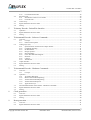
Signal overview
The signal overview of the telemetry encoder and telecommand decoder is shown in figure 1. Note
that the figure only shows the functional signals, not the triplicated inputs and outputs of the FPGA
device.
clk
reset_n
Clock & Reset
cadufall
fecf
Telemetry
reedsolomon
Encoder
caduclk
caduout
pseudo
convolute
bitrate[0:15]
pw0valid_n
pw0clk
PacketWire
Virtual Channel 0
pw0busy
PacketWire
Virtual Channel 1
pw1busy
pw0data
pw1valid_n
pw1clk
pw1data
ocfstatus[0:8]
clcwuart
CLCW
clcwrfavail[0:1]
scid[0:9]
tcpseudo
Telecommand
Decoder
tcactive[0:1]
tcclk[0:1]
tcdata[0:1]
tcvcid[0:5]
Software
Commands
tcuart
Hardware
Commands
tcgpio[0:7]
Figure 1. Signal overview
Copyright Aeroflex Gaisler AB
GR-TMTC-0001
December 2009, Version 1.0.2-1
GAISLER
7
2
Architecture
2.1
Specification
CCSDS TM / TC FPGA
The Telemetry and Telecommand FPGA specification comprises the following elements.
CCSDS compliant Telemetry encoder:
•
•
Input:
•
2 Virtual Channels
•
Synchronous input (bit serial clock, strobe and data, and handshake)
•
Single CLCW input via UART, single CLCW internally
•
9-bit parallel input for project specific OCF
Output:
•
NRZ-L encoding
•
Reed-Solomon and Convolutional encoding (optional)
•
Pin programmable bit rate up to 4 MBPS (after encoding)
•
Bit synchronous output: clock and data
CCSDS compliant Telecommand decoder (software commands):
•
Layers in hardware:
•
•
•
Coding layer
Input:
•
Auto adaptable bit rate up to 4 kBPS
•
Bit synchronous input: clock, qualifier and data
Output:
•
Bit serial output, CADU
CCSDS compliant Telecommand decoder (hardware commands):
•
•
•
Layers in hardware:
•
Coding layer
•
Transfer layer (BD frames only)
•
CLCW internally connected to Telemetry encoder
Input:
•
Auto adaptable bit rate up to 4 kBPS
•
Bit synchronous input: clock, qualifier and data
•
Telecommand Frame with custom cargo, plus CRC
Output:
•
8-bit parallel output (timed)
Copyright Aeroflex Gaisler AB
GR-TMTC-0001
December 2009, Version 1.0.2-1
GAISLER
2.2
8
CCSDS TM / TC FPGA
IP cores
The Telemetry Encoder and Telecommand Decoder is based on the following IP cores:
•
PacketWire Receiver Interface - acts as a slave on the AMBA bus
•
CCSDS/ECSS Telemetry Encoder - GRTM
•
CCSDS/ECSS Telecommand Decoder - Coding Layer - GRTC
•
AMBA AHB bus controller with plug&play - AHBCTRL
•
On-chip RAM with AHB interface and EDAC protection - FTAHBRAM
Additional functionality is implemented:
2.3
•
Telemetry Virtual Channel Generation Function (Virtual Channels 0 and 1)
•
Telemetry CLCW multiplexer
•
UART receiver (CLCW input)
•
UART transmitter (software telecommands output)
•
Hardware telecommand decoder and output pulse generator
Configuration
The telemetry encoder fixed configuration is as follows:
•
fixed transfer frame format, version 00b, Packet Telemetry
•
fixed telemetry transfer frame length of 1115 octets
•
fixed usage of OCF/CLCW, always enabled for all Virtual Channels (Master Channel association, MC_OCF)
•
fixed usage of overwriting No RF Available and No Bit Lock bits in OCF
•
idle telemetry transfer frame generation (Virtual Channel 7)
•
common Master Channel Frame Counter for all Virtual Channels
•
fixed 2 kByte telemetry transmit FIFO
•
4 kByte on-chip EDAC protected RAM per Virtual Channel
•
fixed nominal Attached Synchronization Marker usage
•
fixed NRZ-L telemetry modulation
The telecommand decoder fixed configuration is as follows:
•
fixed NRZ-L telecommand de-modulation
•
fixed telecommand decoder support for CCSDS/ECSS functionality, not ESA PSS
•
telecommand bit serial input data sampled on rising bit clock edge
•
telecommand active signal (bit lock) asserted corresponds to logical one
Copyright Aeroflex Gaisler AB
GR-TMTC-0001
December 2009, Version 1.0.2-1
GAISLER
9
CCSDS TM / TC FPGA
The telemetry encoder does not implement the following:
•
no Advanced Orbiting Systems (AOS) support
•
no Insert Zone (AOS)
•
no Frame Header Error Control (FHEC)
•
no Transfer Frame Secondary Header
•
no Extended Virtual Channel Frame Counter (ECSS)
•
no Punctured Convolutional Encoding
•
no Turbo Encoding
•
no Non-Return-to-Zero Mark (NRZ-M) modulation
•
no Split-Phase Level modulation
•
no Sub-carrier modulation
The telemetry encoder and telecommand decoder provide the following pin programmability:
2.4
•
telemetry and telecommand (hardware commands) Spacecraft Identifier (10 pins)
•
telemetry Frame Error Control Field (FECF/CRC) enable
•
telemetry Reed-Solomon enable (E=16 coding, interleave depth 5, 160 check symbols)
•
telemetry Pseudo Randomization enable
•
telemetry Convolutional Encoder enable (unpunctured rate 1/2 code)
•
telemetry output bit rate configuration (16 pins)
•
telecommand (hardware commands) Virtual Channel Identifier (6 pins)
•
telecommand Pseudo De-randomization enable
Clock and reset
The system clock and the telemetry transmitter clock are derived from an external input.
The device is reset with a single external reset input that need not be synchronous with the system
clock input.
The design has been fixed for the system frequency of 8 000 000 Hz.
The design has been fixed for UART baud rates of 115 200 baud.
Copyright Aeroflex Gaisler AB
GR-TMTC-0001
December 2009, Version 1.0.2-1
GAISLER
2.5
10
CCSDS TM / TC FPGA
Signals
The functional signals are shown in table 1. Note that each external signal is triplicated, with the suffixes _a, _b and _c, as shown in detail in section 36. Note that index 0 is MSB.
Table 1. External signals
Name
Usage
Direction Polarity
Reset
clk
System and telemetry transmitter clock
In
-
-
reset_n
System reset
In
-
-
scid[0:9]
Telemetry and hardware telecommand Spacecraft identifier setting In
-
-
fecf
Telemetry Frame Error Control Field (FECF/CRC) enable
High
-
In
reedsolomon
Telemetry Reed-Solomon encoder enable
In
High
-
pseudo
Telemetry Pseudo-Randomiser encoder enable
In
High
-
convolute
Telemetry Convolutional encoder enable
In
High
-
bitrate[0:15]
Telemetry CADU output bit rate setting
In
-
-
cadufall
Telemetry CADU output clock edge setting
In
High
-
pw0valid_n
Telemetry PacketWire Virtual Channel 0 - packet delimiter
In
Low
-
pw0clk
Telemetry PacketWire Virtual Channel 0 - serial bit clock
In
Rising
-
pw0data
Telemetry PacketWire Virtual Channel 0 - serial bit data
In
-
-
pw0busy
Telemetry PacketWire Virtual Channel 0 - not ready for octet
Out
High
Low
pw1valid_n
Telemetry PacketWire Virtual Channel 1 - packet delimiter
In
Low
-
pw1clk
Telemetry PacketWire Virtual Channel 1 - serial bit clock
In
Rising
-
pw1data
Telemetry PacketWire Virtual Channel 1 - serial bit data
In
-
-
pw1busy
Telemetry PacketWire Virtual Channel 1 - not ready for octet
Out
High
Low
caduclk
Telemetry CADU serial bit clock output
Out
-
Low
caduout
Telemetry CADU serial bit data output
Out
-
Low
clcwuart
Telemetry CLCW asynchronous bit serial UART input
In
Low
-
clcwrfavail[0:1]
Telemetry CLCW RF available indicator input
In
High
-
ocfstatus[0:8]
Telemetry project spectific OCF status data
In
-
-
tcpseudo
Telecommand Pseudo-Derandomiser decoder enable
In
High
-
tcvcid[0:5]
Telecommand (hardware command) Virtual Channel identifier set- In
ting
-
-
tcactive[0:1]
Telecommand CLTU input active indicator (bit lock)
In
High
-
tcclk[0:1]
Telecommand CLTU serial bit clock input
In
Rising
-
tcdata[0:1]
Telecommand CLTU serial bit data input
In
-
-
tcuart
Telecommand (software command) asynchronous bit serial UART
output
Out
-
High
tcgpio[0:3]
Telecommand (hardware command) parallel output
Out
High
Low
tcgpio[4:7]
Telecommand (hardware command) parallel output (tri-stated)
Out
Low
Tri-state
Copyright Aeroflex Gaisler AB
GR-TMTC-0001
December 2009, Version 1.0.2-1
GAISLER
2.6
11
CCSDS TM / TC FPGA
Abbreviations and acronyms
AOS
Advanced Orbiting Systems
ASM
Attached Synchronization Marker
BCH
Bose-Chadhuri-Hacqueghem
CADU
Channel Access Data Unit
CCSDS
Consultative Committee for Space Data Systems
CLCW
Command Link Control Word
CLTU
Command Link Transmission Unit
CRC
Cyclic Redundancy Code
ECSS
European Cooperation on Space Standardization
EDAC
Error Detection and Correction
ESA
European Space Agency
FECF
Frame Error Control Field
FHP
First Header Pointer
FIFO
First In First Out
GF
Galois Field
GPIO
General Purpose Input Output
I/O
Input Output
ID
Identifier
LET
Linear Energy Transfer
LFSR
Linear Feedback Shift Register
LSB
Least Significant Bit/Byte
MC
Master Channel
MSB
Most Significant Bit/Byte
NRZ
Non Return to Zero
OCF
Operational Control Field
PROM
Programmable Read Only Memory
PSR
Pseudo Randomiser
PSS
Procedures, Standards and Specifications
RS
Reed-Solomon
SEL
Single Event Latch-up
SEU
Single Event Upset
SRAM
Static Random Access Memory,
UART
Universal Asynchronous Receiver Transmitter
VC
Virtual Channel
Copyright Aeroflex Gaisler AB
GR-TMTC-0001
December 2009, Version 1.0.2-1
GAISLER
12
3
Conventions
3.1
Consultative Committee for Space Data Systems
CCSDS TM / TC FPGA
Convention according to the Consultative Committee for Space Data Systems (CCSDS) recommendations, applying to all relevant structures:
•
The most significant bit of an array is located to the left, carrying index number zero, and is
transmitted first.
•
An octet comprises eight bits.
General convention, applying to signals and interfaces:
•
Signal names are in mixed case.
•
An upper case '_N' suffix in the name indicates that the signal is active low.
CCSDS n-bit field
most significant
least significant
0
1 to n-2
n-1
Table 2. CCSDS n-bit field definition
3.2
Galois Field
Convention according to the Consultative Committee for Space Data Systems (CCSDS) recommendations, applying to all Galois Field GF(28) symbols:
•
A Galois Field GF(28) symbol comprises eight bits.
•
The least significant bit of a symbol is located to the left, carrying index number zero, and is
transmitted first.
Galois Field GF(28) symbol
least significant
most significant
0
1 to 6
7
Table 3. Galois Field GF(28) symbol definition
Copyright Aeroflex Gaisler AB
GR-TMTC-0001
December 2009, Version 1.0.2-1
GAISLER
3.3
13
CCSDS TM / TC FPGA
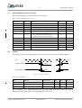
Telemetry Transfer Frame format
The Telemetry Transfer Frame specified in [CCSDS-132.0] and [ECSS-50-03A] is composed of a Primary Header, a Secondary Header, a Data Field and a Trailer with the following structures.
Transfer Frame
Transfer Frame Data Field
Transfer Frame Trailer
Primary
Transfer Frame Header
Secondary (optional)
ket | Packet | Pa
OCF / FECF (optional)
6 octets
variable
variable
0 / 2 /4 / 6 octets
up to 2048 octets
Table 4. Telemetry Transfer Frame format
Transfer Frame Primary Header
Frame Identification
Version
VC
S/C
Id
OCF
Id
Master Channel Virtual Channel
Frame
Frame
Count
Flag
Frame
Data
Count
Field
Status
2 bits
0:1
10 bits
2:11
3 bits
1 bit
12:14
15
2 octets
8 bits
8 bits
16 bits
1 octet
1 octet
2 octets
Table 5. Telemetry Transfer Frame Primary Header format
Frame Data Field Status
Secondary Header Flag
Sync Flag
Packet Order Flag
Segment Length Id
First Header Pointer
1 bit
1 bit
1 bit
2 bits
11 bits
0
1
2
3:4
5:15
2 octets
Table 6. Part of Telemetry Transfer Frame Primary Header format
Transfer Frame Secondary Header (optional)
Secondary Header Identification
Secondary Header Data Field
Secondary Header Version
Secondary Header Length
2 bits
0:1
6 bits
2:7
Custom data
1 octet
up to 63 octets
Table 7. Telemetry Transfer Frame Secondary Header format
Transfer Frame Trailer (optional)
Operational Control Field (optional)
Frame Error Control Field (optional)
0 / 4 octets
0 / 2 octets
Table 8. Telemetry Transfer Frame Trailer format
Copyright Aeroflex Gaisler AB
GR-TMTC-0001
December 2009, Version 1.0.2-1
GAISLER
3.4
14
CCSDS TM / TC FPGA
Reed-Solomon encoder data format
The applicable standards [CCSDS-131.0] and [ECSS-50-01A] specify a Reed-Solomon E=16 (255,
223) code resulting in the frame lengths and codeblock sizes listed in table 9.
Interleave depth
Attached Synchronization Marker
1
4 octets
Transfer Frame
Reed-Solomon Check Symbols
223 octets
32 octets
2
446 octets
64 octets
3
669 octets
96 octets
4
892 octets
128 octets
5
1115 octets
160 octets
8
1784 octets
256 octets
Table 9. Reed-Solomon E=16 codeblocks with Attached Synchronisation Marker
The applicable standards [CCSDS-131.0] also specifies a Reed-Solomon E=8 (255, 239) code resulting in the frame lengths and codeblock sizes listed in table 10.
Interleave depth
Attached Synchronization Marker
Transfer Frame
Reed-Solomon Check Symbols
1
4 octets
239 octets
16 octets
2
478 octets
32 octets
3
717 octets
48 octets
4
956 octets
64 octets
5
1195 octets
80 octets
8
1912 octets
128 octets
Table 10. Reed-Solomon E=8 codeblocks with Attached Synchronisation Marker
3.5
Attached Synchronization Marker
The Attached Synchronization Marker pattern depends on the encoding scheme in use, as specified in
[CCSDS-131.0] and [ECSS-50-01A] as shown in table 11.
Mode
Hexadecimal stream (left to right)
Nominal
1ACFFC1Dh
Table 11. Attached Synchronization Marker hexadecimal pattern
Copyright Aeroflex Gaisler AB
GR-TMTC-0001
December 2009, Version 1.0.2-1
GAISLER
3.6
15
CCSDS TM / TC FPGA
Telecommand Transfer Frame format
The Telecommand Transfer Frame specified in [CCSDS-232.0] and [ECSS-50-04A] is composed of a
Primary Header, a Data Field and a trailer with the following structures.
Transfer Frame
Transfer Frame Primary
Header
Segment Header (optional)
Transfer Frame Data Field
ket | Packet | Pa
Frame Error Control Field
FECF (optional)
5 octets
variable
variable
2 octets
up to 1024 octets
Table 12. Telecommand Transfer Frame format
Transfer Frame Primary Header
Version
Bypass
Control
Reserved
S/C
Virtual
Frame
Frame
Flag
Command
Spare
Id
Channel
Length
Sequence
Flag
Id
Number
2 bits
1 bit
1 bit
2 bits
10 bits
6 bits
10 bits
8 bits
0:1
3
4
5
6:15
16:21
22:31
32:39
2 octets
2 octets
1 octet1
Table 13. Telecommand Transfer Frame Primary Header format
Segment Header (optional)
Sequence Flags
Multiplexer Access Point (MAP) Id
2 bits
6 bits
40:41
42:47
1 octet
Table 14. Transfer Frame Secondary Header format
3.7
Command Link Control Word
The Command Link Control Word (CLCW) can be transmitted as part of the Operation Control Field
(OCF) in a Transfer Frame Trailer. The CLCW is specified in [CCSDS-232.0] and [ECSS-50-04A]
and is listed in table 15.
Command Link Control Word
Control Word Type
Version Number
Status Field
COP in Effect
Virtual Channel Identifier
Reserved Spare
0
1:2
3:5
6:7
8:13
14:15
1 bit
2 bits
3 bits
2 bits
6 bits
2 bits
No RF Available
No Bit Lock
Lock Out
Wait
Retransmit FARM B Reserved
Counter
Spare
Report Value
16
17
18
19
20
21:22
23
1 bit
1 bit
1 bit
1 bit
1 bit
2 bits
1 bit
24:31
Table 15. Command Link Control Word
Copyright Aeroflex Gaisler AB
GR-TMTC-0001
December 2009, Version 1.0.2-1
GAISLER
3.8
16
CCSDS TM / TC FPGA
Space Packet
The Source Packet defined in the CCSDS [CCSDS-133.0] recommendation and is listed in table 16.
Space Packet
Primary Header
Packet Packet Identification
Version Type Secondary
Application
Number
Header Flag
Process Id
Packet Data Field
Packet Sequence Control
Packet
Sequence
Flags
Sequence
Count
Secondary
Header
Data
(optional)
Length
0:2
3
4
5:15
16:17
18:31
32:47
3 bits
1 bit
1 bit
11 bits
2 bits
14 bits
16 bits
User
Data
variable
Field
Packet Error
Control
(optional)
variable
variable
Table 16. Source Packet and Telemetry Packet format
3.9
Asynchronous bit serial data format
The asynchronous bit serial interface complies to the data format defined in [EIA232]. It also complies to the data format and waveform shown in table 17 and figure 3. The interface is independent of
the transmitted data contents. Positive logic is considered for the data bits. The number of stop bits
can optionally be either one or two. The parity bit can be optionally included.
Asynchronous
bit serial format
start
D0
first
lsb
General data format
i = {0, n}
D1
D2
D3
D4
D5
D6
D7
parity stop
msb
stop
last
8*i+7 8*i+6 8*i+5 8*i+4 8*i+3 8*i+2 8*i+1 8*i
last
first
Table 17. Asynchronous bit serial data format
3.10
Project specific Operation Control Field
The project specific Operation Control Field is according to [CCSDS-132.0] and is listed in table 18.
Operation Control Field
Type Flag
Project/Reserved
N/A
No RF Available
No Bit Lock
N/A
Discrete inputs
0
1
2:15
16
17
18:22
23:31
1 bit
1 bit
14 bits
1 bit
1 bit
5 bits
9 bits
’1’
’0’
zero
zero
ocfstatus[0:8]
Type-2 Report
Project Specific
-
-
From input pins
Same as for CLCW (Type-1 Report)
From input pins
From input pins
Table 18. Project specific Operation Control Field
Copyright Aeroflex Gaisler AB
GR-TMTC-0001
December 2009, Version 1.0.2-1
GAISLER
3.11
17
CCSDS TM / TC FPGA
Waveform formats
The design and generates the waveform formats shown in the following figures.
Delimiter
Clock
0
Data
1
2
3
4
5
6
7
0
1
2
3
6
7
0
1
2
3
4
5
6
7
Figure 2. Synchronous bit serial protocol / waveform
Start
bit
Data
Stop
bits
Start LSB
MSB Stop
Start LSB
MSB Stop Stop
Start
bit
Parity Stop
bits
Data
Start LSB
MSB
P
Stop
Start LSB
MSB
P
Stop Stop
Break
Start
Stop
Figure 3. Asynchronous bit serial protocol / waveform
Delimiter
Clock
Data
0
1
2
3
4
5
6
7
n-8 n-7 n-6 n-5 n-4 n-3 n-2 n-1
MSB
LSB
Figure 4. Telecommand input protocol / waveform
Copyright Aeroflex Gaisler AB
GR-TMTC-0001
December 2009, Version 1.0.2-1
GAISLER
18
4
Telemetry Encoder
4.1
Overview
CCSDS TM / TC FPGA
The CCSDS/ECSS/PSS Telemetry Encoder implements part of the Data Link Layer, covering the
Protocol Sub-layer and the Frame Synchronization and Coding Sub-layer and part of the Physical
Layer of the packet telemetry encoder protocol. The Telemetry Encoder comprises several encoders
and modulators implementing the Consultative Committee for Space Data Systems (CCSDS) recommendations, European Cooperation on Space Standardization (ECSS) and the European Space
Agency (ESA) Procedures, Standards and Specifications (PSS) for telemetry and channel coding.
The encoder comprises the following:
•
Packet Telemetry Encoder (TM)
•
Reed-Solomon Encoder
•
Pseudo-Randomiser (PSR)
•
Non-Return-to-Zero Level encoder (NRZ-L)
•
Convolutional Encoder (CE)
•
Clock Divider (CD)
Virtual Channel
Generation
AMBA
AHB
Master
DMA
FIFO
Master Channel
Generation
Idle Frame
Generation
OCF
FSH
Master Channel Mux
AMBA
APB
Slave
All Frame Generation
Insert Zone
Coding Sub-Layer
AMBA APB
Virtual Channel & Master Channel
Frame Services
Attached Sync Mark
System clock domain
Reed-Solomon
Pseudo-Randomiser
NRZ-L
Convolutional
-
GRTM
Octet clock domain
Transponder
clock domain
Clock
Divider
Physical Layer
AMBA AHB
Virtual Channel Mux
Data Link Protocol Sub-Layer
Note that the PacketWire input interface is described separately. Note that the PacketWire interfaces
and corresponding Virtual Channel Generation function and buffer memories are not shown in the
block diagram below, as is the case for the CLCW input UART, project specific OCF status inputs and
the CLCW multiplexing function.
Telemetry output
Figure 5. Block diagram
Copyright Aeroflex Gaisler AB
GR-TMTC-0001
December 2009, Version 1.0.2-1
GAISLER
4.2
19
CCSDS TM / TC FPGA
Layers
4.2.1
Introduction
The relationship between Packet Telemetry standard and the Open Systems Interconnection (OSI) reference model is such that the OSI Data Link Layer corresponds to two separate layer, namely the Data
Link Protocol Sub-layer and Synchronization and Channel Coding Sub-Layer.
4.2.2
Data Link Protocol Sub-layer
The following functionality is not implemented in the core:
•
Packet Processing
•
Virtual Channel Frame Service
•
Master Channel Frame Service
The following functionality is implemented in the core:
•
Virtual Channel Generation (for Idle Frame generation only)
•
Virtual Channel Multiplexing (for all frames)
•
Master Channel Generation (for all frames)
•
Master Channel Multiplexing (not implemented, only single Spacecraft Identifier supported)
•
All Frame Generation (for all frames)
4.2.3
Synchronization and Channel Coding Sub-Layer
The following functionality is implemented in the core:
•
Attached Synchronization Marker
•
Reed-Solomon coding
•
Pseudo-Randomiser
•
Convolutional coding
4.2.4
Physical Layer
The following functionality is implemented in the core:
•
4.3
Non-Return-to-Zero modulation
Data Link Protocol Sub-Layer
4.3.1
Physical Channel
The configuration of a Physical Channel covers the following parameters:
•
Transfer Frame Length is fixed to 1115 octets
•
Transfer Frame Version Number is fixed to 0
Copyright Aeroflex Gaisler AB
GR-TMTC-0001
December 2009, Version 1.0.2-1
GAISLER
20
4.3.2
CCSDS TM / TC FPGA
Virtual Channel Frame Service
The Virtual Channel Frame Service is implemented via Direct Memory Accesses to on-chip memory.
The Virtual Channel Generation functions for Virtual Channel 0 and 1 create such Transfer Frames
that are transferred via DMA as part of the Virtual Channel Frame Service.
4.3.3
Virtual Channel Generation - Virtual Channels 0 and 1
There is a Virtual Channel Generation function for each of Virtual Channels 0 and 1. The channels
have each an on-chip memory buffer to store two complete Transfer Frames.
Each Virtual Channel Generation function receives data from the PacketWire interface that are stored
in the on-chip buffer memory that is EDAC protected.
The function supports:
•
Transfer Frame Primary Header insertion
•
Transfer Frame Data Field insertion (with support for different lengths due to OCF and FECF)
•
First Header Pointer (FHP) handling and insertion
The function keeps track of the number of octets received and the packet boundaries in order to calculated the First Header Pointer (FHP). The data are stored in pre-allocated slots in the buffer memory
comprising complete Transfer Frames. The module fully supports the FHP generation and does not
require any alignment of the packets with the Transfer Frame Data Field boundary. The buffer memory space allocated to each Virtual Channel is treated as a circular buffer.
When a complete Transfer Frame Data Field has been inserted, the function will generate a busy signal on the PacketWire interface, but accepts and handles an overrun up to two octets.
The function communicates with the Virtual Channel Frame Service by means of the on-chip buffer
memory.
4.3.4
Virtual Channel Generation - Idle Frames
The Virtual Channel Generation function is used to generate the Virtual Channel Counter for Idle
Frames as described here below.
4.3.5
Virtual Channel Multiplexing
The Virtual Channel Multiplexing Function is used to multiplex Transfer Frames of different Virtual
Channels of a Master Channel. Virtual Channel Multiplexing in the core is performed between two
sources: Transfer Frames provided through the Virtual Channel Frame Service and Idle Frames. Note
that multiplexing between different Virtual Channels is implicitly implemented, Virtual Channel 0
and 1 are each allocated 50% of the bandwidth.
The Virtual Channel Frame Service user interface is described above. The Idle Frame generation is
described hereafter.
The Spacecraft ID to be used for Idle Frames is pin configurable. The Virtual Channel ID to be used
for Idle Frames is fixed to 7.
Master Channel Counter generation for Idle Frames is done as part of the Master Channel Generation
function described in the next section.
The Virtual Channel Counter generation for Idle Frames is always enabled and generated in the Virtual Channel Generation function described above.
Copyright Aeroflex Gaisler AB
GR-TMTC-0001
December 2009, Version 1.0.2-1
GAISLER
21
4.3.6
CCSDS TM / TC FPGA
Master Channel Generation
The Master Channel Counter is generated for all frames on the master channel.
The Operational Control Field (OCF) is generated from a 32-bit input, via the Command Link Control
Word (CLCW) UART input, internal from the Telecommand Decoder - Hardware Commands, or
from the ocfstatus[0:8] input pins for the project specific OCF. This is done for all frames on the master channel (MC_OCF).
The transmit order repeats every four Transfer Frames and is as follows:
•
CLCW from the CLCLW UART input is transmitted in Transfer Frames with an odd Transfer
Frame Master Channel Counter value, i.e. ends with the least-significant-bits "00" or "10"
•
CLCW from the internal hardware commands is transmitted in Transfer Frames with a Transfer
Frame Master Channel Counter value that ends with the least-significant-bits "01"
•
the project specific OCF is transmitted in Transfer Frames with a Transfer Frame Master Channel
Counter value that ends with the least-significant-bits "11".
Note that bit 16 (No RF Available) and 17 (No Bit Lock) of the CLCW and project specific OCF are
taken from information carried on discrete inputs clcwavail[1:0] and tcactive[1:0].
An asynchronous bit serial input UART is used for receiving the CLCW from the user. The protocol is
fixed to 115200 baud, 1 start bit, 8 data bits, 1 stop bit, with a BREAK command for message delimiting (sending 13 bits of logical zero).
Table 19.CLCW transmission protocol
Byte
Number
CLCW bits
CLCW contents
First
[0:7]
Control Word Type
CLCW
Version
Number
Second
[8:15]
Virtual Channel
Identifier
Reserved Field
Third
[16:23]
No RF
Available
No Bit
Lock
Fourth
[24:31]
Report Value
Fifth
N/A
[RS232 Break Command]
4.3.7
Status
Field
Lock
Out
COP In Effect
Wait
Retransmit
Farm B
Counter
Report
Type
Master Channel Frame Service
The Master Channel Frame Service is not implemented.
4.3.8
Master Channel Multiplexing
The Master Channel Multiplexing Function is not implemented.
4.3.9
All Frame Generation
The All Frame Generation functionality operates on all transfer frames of a Physical Channel.
Frame Error Control Field (FECF) generation can be enabled and disabled by means of external pin.
Copyright Aeroflex Gaisler AB
GR-TMTC-0001
December 2009, Version 1.0.2-1
GAISLER
4.4
22
CCSDS TM / TC FPGA
Synchronization and Channel Coding Sub-Layer
4.4.1
Attached Synchronization Marker
The 32-bit Attached Synchronization Marker is placed in front of each Transfer Frame as per
[CCSDS-131.0] and [ECSS-50-03A].
4.4.2
Reed-Solomon Encoder
The CCSDS recommendation [CCSDS-131.0] and ECSS standard [ECSS-50-03A] specify ReedSolomon codes, one (255, 223) code. The ESA PSS standard [PSS-04-103] only specifies the former
code. Although the definition style differs between the documents, the (255, 223) code is the same in
all three documents. The definition used in this document is based on the PSS standard [PSS-04-103].
The Reed-Solomon encoder is compliant with the coding algorithms in [CCSDS-131.0] and [ECSS50-03A]:
•
there are 8 bits per symbol;
•
there are 255 symbols per codeword;
•
the encoding is systematic:
•
for E=16 or (255, 223), the first 223 symbols transmitted are information symbols, and the last 32
symbols transmitted are check symbols;
•
the E=16 code can correct up to 16 symbol errors per codeword;
•
the field polynomial is
8
6
4
3
2
f esa ( x ) = x + x + x + x + x + x + 1
•
the code generator polynomial for E=8 is
135
g esa ( x ) =
∏
16
i
(x + α ) =
i = 120
∑ gj ⋅ x
j
j=0
for which the highest power of x is transmitted first;
•
the code generator polynomial for E=16 is
143
g esa ( x ) =
∏
32
i
(x + α ) =
i = 112
∑ gj ⋅ x
j
j=0
for which the highest power of x is transmitted first;
•
interleaving is supported for depth I = {1 to 8}, where information symbols are encoded as I
codewords with symbol numbers i + j*I belonging to codeword i {where 0 ≤ i < I and 0 ≤ j <
255};
•
shortened codeword lengths are supported;
Copyright Aeroflex Gaisler AB
GR-TMTC-0001
December 2009, Version 1.0.2-1
GAISLER
•
23
the input and output data from the encoder are in the representation specified by the following
transformation matrix Tesa, where i0 is transferred first
ι0 ι 1 ι2 ι 3 ι4 ι5 ι 6 ι7 = α7 α6 α5 α4 α3 α2 α 1 α0
•
0
0
1
× 0
0
0
0
0
0
1
0
0
0
0
1
1
1
0
0
0
1
1
1
1
1
1
0
0
1
0
1
1
0
1
0
1
1
1
1
1
1
1
1
0
1
0
0
0
1
1
1
0
1
1
0
1
1
1
1
1
1
1
1
1
0
1
1
1
0
1
0
1
1
1
0
1
1
0
0
1
1
1
1
0
0
1
0
0
0
1
1
1
0
1
1
0
1
1
1
0
0
0
1
0
the following matrix T-1esa specifying the reverse transformation
α7 α 6 α5 α4 α3 α2 α1 α0 = ι0 ι 1 ι2 ι3 ι 4 ι5 ι 6 ι7
•
CCSDS TM / TC FPGA
1
0
0
× 0
1
0
0
1
1
1
0
1
0
1
0
0
1
0
0
0
0
0
0
0
the Reed-Solomon output is non-return-to-zero level encoded.
The Reed-Solomon Encoder encodes a bit stream from preceding encoders and the resulting symbol
stream is output to subsequent encoder and modulators. The encoder generates codeblocks by receiving information symbols from the preceding encoders which are transmitted unmodified while calculating the corresponding check symbols which in turn are transmitted after the information symbols.
The check symbol calculation is disabled during reception and transmission of unmodified data not
related to the encoding. The calculation is independent of any previous codeblock and is perform correctly on the reception of the first information symbol after a reset.
Each information symbol corresponds to an 8 bit symbol. The symbol is fed to a binary network in
which parallel multiplication with the coefficients of a generator polynomial is performed. The products are added to the values contained in the check symbol memory and the sum is then fed back to
the check symbol memory while shifted one step. This addition is performed octet wise per symbol.
This cycle is repeated until all information symbols have been received. The contents of the check
symbol memory are then output from the encoder. The encoder is based on a parallel architecture,
including parallel multiplier and adder.
Copyright Aeroflex Gaisler AB
GR-TMTC-0001
December 2009, Version 1.0.2-1
GAISLER
4.4.3
24
CCSDS TM / TC FPGA
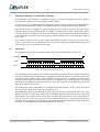
Pseudo-Randomiser
The Pseudo-Randomiser (PSR) generates a bit sequence according to [CCSDS-131.0] and [ECSS-5003A] which is xor-ed with the data output of preceding encoders. This function allows the required bit
transition density to be obtained on a channel in order to permit the receiver on ground to maintain bit
synchronization.
The polynomial for the Pseudo-Randomiser is h (x) = x8+x7+x5+x3+1 and is implemented as a
Fibonacci version (many-to-one implementation) of a Linear Feedback Shift Register (LFSR). The
registers of the LFSR are initialized to all ones between Transfer Frames. The Attached Synchronization Marker (ASM) is not effected by the encoding.
data in
x8
x7
x6
x5
x4
x3
x2
data out
x1
initialise to all zero
Figure 6. Pseudo-randomiser
4.4.4
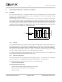
Convolutional Encoder
The Convolutional Encoder (CE) implements the basic convolutional encoding scheme. The ESA
PSS standard [PSS-04-103] specifies a basic convolutional code without puncturing. This basic convolutional code is also specified in the CCSDS recommendation [CCSDS-131.0] and ECSS standard
[ECSS-50-03A], which in addition specifies a punctured convolutional code.
The basic convolutional code has a code rate of 1/2, a constraint length of 7, and the connection vectors G1 = 1111001b (171 octal) and G2 = 1011011b (133 octal) with symbol inversion on output path,
where G1 is associated with the first symbol output.
G1
data out G1
1
data in
x6
x5
x4
x3
x2
x1
data out
2
data out G2
G2
Figure 7. Unpuctured convolutional encoder
4.5
Physical Layer
4.5.1
Non-Return-to-Zero Level encoder
The Non-Return-to-Zero Mark encoder (NRZ-L) encodes differentially a bit stream from preceding
encoders according to [ECSS-50-05A]. The waveform is shown in figure 8. Both data and the
Attached Synchronization Marker (ASM) are affected by the coding. When the encoder is not
enabled, the bit stream is by default non-return-to-zero level encoded.
Copyright Aeroflex Gaisler AB
GR-TMTC-0001
December 2009, Version 1.0.2-1
GAISLER
25
Symbol:
1
0
CCSDS TM / TC FPGA
0
1
0
1
1
0
NRZ-L
Figure 8. NRZ-L waveform
4.5.2
Clock Divider
The clock divider provides clock enable signals for the telemetry and channel encoding chain. The
clock enable signals are used for controlling the bit rates of the different encoder and modulators.
The source for the bit rate frequency is the system clock input. The system clock input can be divided
to a degree 216. The divider can be configured during operation to divide the bit rate clock frequency
from 1/2 to 1/216.
The bit rate frequency is based on the output frequency of the last encoder in a coding chain. No
actual clock division is performed, since clock enable signals are used. No clock multiplexing is performed in the core. The clock divider supports clock rate increases for the following encoder and rate:
Convolutional Encoder, rate 1/2. The polarity of the output clock is pin programmable.
The resulting nominal symbol rate and telemetry rate are depended on what encoders and modulators
are enabled. The following variables are used in the tables hereafter: f = input system clock frequency,
n = bitrate[0:15] input field +1.
Table 20. Data rates
Coding & Modulation
Telemetry rate
Convolutional rate Output symbol rate
Output clock frequency
f/n
f/n
f/n
Convolutional
f / (n * 2)
f/n
f/n
f/n
n = 1 is not supported, i.e. bitrate[0:15] input equals 0
n = 65536 is the larget value supported without emergency rate usage, i.e. bitrate[0:15] input equals 0xFFFF
n = 8192 is the largest value supported with emergency rate usage, i.e. bitrate[0:15] input equals 0x1FFF
n should be an even number, i.e. bitrate[0:15] input should be uneven to generate output symbol clock with 50% duty cycle
The clock divider also supports an emergency rate, controlled via Hardware Command, i.e. OUTPUT(8). The value of the bitrate[0:15] input is multiplied by 8 and 1 is added. The resulting output
symbol rate generation is shown in the following examples.
Nominal mode, OUTPUT(8)=0:
•
bitrate[0:15] = 0x0000 => n=1 => illegal
•
bitrate[0:15] = 0x0001 => n=2 => f/2
•
bitrate[0:15] = 0x0002 => n=3 => f/3
•
bitrate[0:15] = 0x0003 => n=4 => f/4
•
bitrate[0:15] = 0x0004 => n=5 => f/5
Emergency mode, OUTPUT(8)=1:
•
bitrate[0:15] = 0x0000 => illegal
•
bitrate[0:15] = 0x0001 => 0x0009 => n=10 => f/10
•
bitrate[0:15] = 0x0002 => 0x0011 => n=18 => f/18
•
bitrate[0:15] = 0x0003 => 0x0019 => n=26 => f/26
•
bitrate[0:15] = 0x0004 => 0x0021 => n=34 => f/34
Copyright Aeroflex Gaisler AB
GR-TMTC-0001
December 2009, Version 1.0.2-1
GAISLER
4.6
26
CCSDS TM / TC FPGA
Connectivity
The output from the Packet Telemetry encoder can be connected to:
•
Reed-Solomon encoder
•
Pseudo-Randomiser
•
Non-Return-to-Zero Level encoder
•
Convolutional encoder
The input to the Reed-Solomon encoder can be connected to:
•
Packet Telemetry encoder
The output from the Reed-Solomon encoder can be connected to:
•
Pseudo-Randomiser
•
Non-Return-to-Zero Level encoder
•
Convolutional encoder
The input to the Pseudo-Randomiser (PSR) can be connected to:
•
Packet Telemetry encoder
•
Reed-Solomon encoder
The output from the Pseudo-Randomiser (PSR) can be connected to:
•
Non-Return-to-Zero Level encoder
•
Convolutional encoder
The input to the Non-Return-to-Zero Level encoder (NRZ-L) can be connected to:
•
Packet Telemetry encoder
•
Reed-Solomon encoder
•
Pseudo-Randomiser
The output from the Non-Return-to-Zero Level encoder (NRZ-L) can be connected to:
•
Convolutional encoder
The input to the Convolutional Encoder (CE) can be connected to:
•
Packet Telemetry encoder
•
Reed-Solomon encoder
•
Pseudo-Randomiser
•
Non-Return-to-Zero Level encoder
Copyright Aeroflex Gaisler AB
GR-TMTC-0001
December 2009, Version 1.0.2-1
GAISLER
4.7
27
CCSDS TM / TC FPGA
Signal definitions and reset values
The signals and their reset values are described in table 21.
Table 21. Signal definitions and reset values
4.8
Signal name
Type
Function
Active
Reset value
clcwrfavail[0:1]
Input, async
RF Available
High
-
clcwuart
Input, async
CLCW UART input
-
-
ocfstatus[0:8]
Input, async
Project specific OCF status data input
-
-
caduout
Output
Serial bit data, output at caduclk edge (selectable)
-
-
caduclk
Output
Serial bit data clock
Rising
Logical 0
cadufall
Input, static
Serial bit data clock edge selection:
0 = rising caduclk edge at caduout change
1 = falling caduclk edge at caduout change
High
-
fecf
Input, static
Enable Frame Error Control Field (FECF/CRC)
High
-
reedsolomon
Input, static
Enable Reed-Solomon encoder
High
-
pseudo
Input, static
Enable Pseudo Randomizer encoder
High
-
convolute
Input, static
Enable Convolutional encoder
High
-
bitrate[0:15]
Input, static
Telemetry bit rate selection
-
-
scid[0:9]
Input, static
Telemetry Spacecraft Identifier
-
-
Timing
The timing waveforms and timing parameters are shown in figure 9 and are defined in table 22.
clk
caduout, caduclk
tGRTM0
clcwrfavail[], clcwuart, ocfstatus[]
tGRTM1
tGRTM0
tGRTM2
Figure 9. Timing waveforms
Table 22. Timing parameters
Name
Parameter
Reference edge
Min
Max
Unit
tGRTM0
clock to output delay
rising clk edge
0
30
ns
tGRTM1
input to clock hold
rising clk edge
-
-
ns
tGRTM2
input to clock setup
rising clk edge
-
-
ns
Note: The inputs are re-synchronized inside the core. The signals do not have to meet any setup or
hold requirements. Static signals should not change between resets.
Copyright Aeroflex Gaisler AB
GR-TMTC-0001
December 2009, Version 1.0.2-1
GAISLER
5
28
CCSDS TM / TC FPGA
Telemetry Encoder - PacketWire Interface
The PacketWire (PW) interface to a telemetry encoder is a simple bit synchronous protocol. There is
one PacketWire interface for each telemetry Virtual Channel.
The data can be any CCSDS supported packets. The interface comprises three input signals; bit data,
bit clock and packet delimiter. There is an additional discrete signal provided for busy signalling.
Data should consist of multiples of eight bits otherwise the last bits will be lost. The input packet
delimiter signal is used to delimit packets. It should be asserted while a packet is being input, and deasserted in between. In addition, the input packet delimiter signal should define the octet boundaries
in the input data stream, the first octet explicitly and the following octets each subsequent eight bit
clock cycles.
The interface is based on the de facto standard PacketWire interface used by the European Space
Agency (ESA). At the time of writing there were no relevant documents available from the European
Cooperation for Space Standardization (ECSS).
5.1
Operation
The PacketWire interface accepts and generates the waveform format shown in figure 10.
Delimiter
Clock
Data
0
1
2
3
4
5
6
7
0
1
2
3
6
7
0
1
2
3
4
5
6
7
Figure 10. Synchronous bit serial waveform
The PacketWire protocol follows the CCSDS transmission convention, the most significant bit being
sent first. Transmitted data should consist of multiples of eight bits otherwise the last bits will be lost.
The input message delimiter port is used to delimit messages (packets). It should be asserted while a
message is being input, and deasserted in between. In addition, the message delimiter port should
define the octet boundaries in the data stream, the first octet explicitly and the following octets each
subsequent eight bit clock cycles.
The maximum receiving input baud rate is defined as half the frequency of the system clock input.
There is no lower limit for the input bit rate in the receiver.
The handshaking between the PacketWire links and the interface is implemented with a busy port.
When a message is sent, the busy signal on the PacketWire input link will be asserted as soon as the
input interface is not ready to receive more data, it will then be deasserted as soon as the interface is
ready to receive the next octet. This gives the transmitter ample time to stop transmitting after the
completion of an octet and wait for the busy signal deassertion before starting the transmission of the
next octet. The handshaking is continued through out the message.
Copyright Aeroflex Gaisler AB
GR-TMTC-0001
December 2009, Version 1.0.2-1
GAISLER
5.2
29
CCSDS TM / TC FPGA
Signal definitions and reset values
The signals and their reset values are described in table 23.
Table 23. Signal definitions and reset values
5.3
Signal name
Type
Function
Active
Reset value
pw*valid_n
Input
Delimiter: This input port is the message delimiter
for the input interface. It should be deasserted
between messages.
Low
-
pw*clk
Input
Bit clock: This input port is the PacketWire bit clock. Rising
The receiver registers are clocked on the rising edge.
-
pw*data
Input
Data: This input port is the serial data input for the
interface. Data are sampled on the rising pw*clk
edge when pw*valid_n is asserted.
-
-
pw*busy
Output
Not ready for octet: This port indicates whether the
receiver is ready to receive one octet.
High
Logical 0
Timing
The timing waveforms and timing parameters are shown in figure 11 and are defined in table 24.
clk
pw*busy
tGRPW0
tGRPW0
pw*clk
tGRPW1
tGRPW2
pw*data
Figure 11. Timing waveforms
Table 24. Timing parameters
Name
Parameter
Reference edge
Min
Max
Unit
tGRPW0
clock to output delay
rising clk edge
0
30
ns
tGRPW1
input to clock hold
rising pw*clk edge
20
-
ns
tGRPW2
input to clock setup
rising pw*clk edge
20
-
ns
tGRPW3
pw*valid_n to pw*clk edge
rising pw*clk edge
20
-
ns
tGRPW3
pw*valid_n de-asserted period
-
4
Copyright Aeroflex Gaisler AB
GR-TMTC-0001
system clock
periods
December 2009, Version 1.0.2-1
GAISLER
30
CCSDS TM / TC FPGA
6
Telecommand Decoder - Software Commands
6.1
Overview
The Telecommand Decoder is compliant with the Packet Telecommand protocol and specification
defined by the CCSDS recommendations stated in [CCSDS-231.0]. The Telecommand Decoder
implements the Coding Layer (CL).
In the Coding Layer (CL), the telecommand decoder receives bit streams on multiple channel inputs.
The streams are assumed to have been generated in accordance with the Physical Layer specifications.
The decoder searches all input streams simultaneously until a start sequence is detected. Only one of
the channel inputs is selected for further reception. The selected stream is bit-error corrected and the
resulting corrected information is passed to the user. The corrected information received in the CL is
transfer by means of a UART to the on-board processor.
NRZ-L
Telecommand input
Physical Layer
Start sequence search
BCH Decoder
UART
Pseudo-Derandomizer
User
Coding Sub-Layer
GRTC
Figure 12. Block diagram
6.1.1
Concept
A telecommand decoder in this concept is mainly implemented by software in the on-board processor.
The supporting hardware in the GRTC core implements the Coding Layer, which includes synchronisation pattern detection, channel selection, codeblock decoding, and output of corrected codeblocks.
The telemetry encoder hardware provides a UART via which the Command Link Control Word
(CLCW) is made available. The CLCW is to be generated by the software.
A complete CCSDS packet telecommand decoder can be realized at software level according to the
latest available standards, staring from the Transfer Layer.
6.1.2
Functions and options
The telecommand decoder only implements the Coding Layer (CL). All other layers are to be implemented in software. A Command Pulse Distribution Unit (CPDU) is not implemented.
The following function is programmable by means of a configuration pin:
•
Pseudo-De-Randomisation
The following functions are fixed:
•
Polarity of RF Available and Bit Lock inputs (active high)
•
Edge selection for input channel clock (rising edge)
•
NRZ-L decoding
Copyright Aeroflex Gaisler AB
GR-TMTC-0001
December 2009, Version 1.0.2-1
GAISLER
6.2
31
CCSDS TM / TC FPGA
Coding Layer (CL)
The Coding Layer synchronises the incoming bit stream and provides an error correction capability
for the Command Link Transmission Unit (CLTU). The Coding Layer receives a dirty bit stream
together with control information on whether the physical channel is active or inactive for the multiple input channels.
The bit stream is assumed to be NRZ-L encoded, as the standards specify for the Physical Layer.
There are no assumptions made regarding the periodicity or continuity of the input clock signal while
an input channel is inactive. The most significant bit (bit 0) is received first.
Searching for the Start Sequence, the Coding Layer finds the beginning of a CLTU and decodes the
subsequent codeblocks. As long as no errors are detected, or errors are detected and corrected, the
Coding Layer passes clean blocks of data to the Transfer Layer which is implemented in software.
When a codeblock with an uncorrectable error is encountered, it is considered as the Tail Sequence, its
contents are discarded and the Coding Layer returns to the Start Sequence search mode.
The Coding Layer supports to enable an optional de-randomiser according to [CCSDS-231.0].
6.2.1
Synchronisation and selection of input channel
Synchronisation is performed by means of bit-by-bit search for a Start Sequence on the channel
inputs. The detection of the Start Sequence is tolerant to a single bit error anywhere in the Start
Sequence pattern. The Coding Layer searches both for the specified pattern as well as the inverted
pattern. When an inverted Start Sequence pattern is detected, the subsequent bit-stream is inverted till
the detection of the Tail Sequence.
The detection is accomplished by a simultaneous search on all active channels. The first input channel
where the Start Sequence is found is selected for the CLTU decoding. The selection mechanism is
restarted on any of the following events:
•
The input channel active signal is de-asserted, or
•
a Tail Sequence is detected, or
•
a Codeblock rejection is detected, or
•
an abandoned CLTU is detected, or the clock time-out expires.
As a protection mechanism in case of input failure, a clock time-out is provided for all selection
modes. The clock time-out expires when no edge on the bit clock input of the selected input channel
in decode mode has been detected for a period of 2**24 system clock cycles.
6.2.2
Codeblock decoding
The received Codeblocks are decoded using the standard (63,56) modified BCH code. Any single bit
error in a received Codeblock is corrected. A Codeblock is rejected as a Tail Sequence if more than
one bit error is detected.
6.2.3
De-Randomiser
In order to maintain bit synchronisation with the received telecommand signal, the incoming signal
must have a minimum bit transition density. If a sufficient bit transition density is not ensured for the
channel by other methods, the randomiser is required. Its use is optional otherwise. The presence or
absence of randomisation is fixed for a physical channel and is managed (i.e., its presence or absence
is not signalled but must be known a priori by the spacecraft and ground system). A random sequence
is exclusively OR-ed with the input data to increase the frequency of bit transitions. On the receiving
Copyright Aeroflex Gaisler AB
GR-TMTC-0001
December 2009, Version 1.0.2-1
GAISLER
32
CCSDS TM / TC FPGA
end, the same random sequence is exclusively OR-ed with the decoded data, restoring the original
data form. At the receiving end, the de-randomisation is applied to the successfully decoded data. The
de-randomiser remains in the “all-ones” state until the Start Sequence has been detected. The pattern
is exclusively OR-ed, bit by bit, to the successfully decoded data (after the Error Control Bits have
been removed). The de-randomiser is reset to the “all-ones” state following a failure of the decoder to
successfully decode a codeblock or other loss of input channel.
6.2.4
Design specifics
The coding layer is supporting 2 channel inputs. The CCSDS/ECSS (1024 octets) standard maximum
frame length is supported. The former allows more than 37 codeblocks to be received. A codeblock is
fixed to 56 information bits (as per CCSDS/ECSS).
The Pseudo-Randomiser decoder is included (as per CCSDS/ECSS), its usage being input signal programmable. The Physical Layer input can be NRZ-L modulated, allowing for polarity ambiguity.
Note: If input clock disappears, it will also affect the codeblock acquired immediately before the
codeblock just being decoded (accepted by [PSS-04-151]).
In state S1, all active inputs are searched for start sequence, there is no priority search, only round
robin search. The search for the start sequence is sequential over all inputs: maximum input frequency
= system frequency / 4.
The [PSS-04-151] specified CASE-1 and CASE-2 actions are implemented according to aforementioned specification, not leading to aborted frames.
Extended E2 handling is implemented:
•
E2b Channel Deactivation - selected input becomes inactive in S3
•
E2c
•
E2d Channel Deactivation - selected input is timed-out in S3
(design choice being: S3 => S1, abandoned frame)
6.2.5
Channel Deactivation - too many codeblocks received in S3
Data formatting
When in the decode state, each candidate codeblock is decoded in single error correction mode as
described hereafter.
6.2.6
CLTU Decoder State Diagram
+----------+
+----------+
|
|
S1
|
| INACTIVE |-----E1---->|
+----------+
S2
|<----E4-----|
S3
|
ACTIVE
|-----E3---->|
DECODE
|
|
|<----E2a----|
|<----E2c----|
|
|
|
|
|
|<----------------E2b----------------|
|
|
|<----------------E2d----------------|
|
+----------+
+----------+
|
+----------+
Note that the diagram has been improved with explicit handling of different E2 possibilities listed
below.
Copyright Aeroflex Gaisler AB
GR-TMTC-0001
December 2009, Version 1.0.2-1
GAISLER
33
CCSDS TM / TC FPGA
State Definition:
S1
Inactive
S2
Search
S3
Decode
Event Definition:
E1
Channel Activation
E2a
Channel Deactivation - all inputs are inactive
E2b Channel Deactivation - selected becomes inactive (CB=0 -> frame abandoned)
E2c
Channel Deactivation - too many codeblocks received (all -> frame abandoned)
E2d Channel Deactivation - selected is timed-out (all -> frame abandoned)
E3
Start Sequence Found
E4
Codeblock Rejection (CB=0 -> frame abandoned)
6.2.7
Nominal
A: When the first “Candidate Codeblock” (i.e. “Candidate Codeblock” 0, which follows Event 3
(E3):START SEQUENCE FOUND) is found to be error free, or if it contained an error which has
been corrected, its information octets are transferred to the remote ring buffer as shown in Table 3.1.
At the same time, a “Start of Candidate Frame” flag is written to bit 0 or 16, indicating the beginning
of a transfer of a block of octets that make up a “Candidate Frame”. There are two cases that are handled differently as described in the next sections.CASE 1
When an Event 4 – (E4): CODEBLOCK REJECTION – occurs for any of the 37 possible “Candidate
Codeblocks” that can follow Codeblock 0 (possibly the tail sequence), the decoder returns to the
SEARCH state (S2), with the following actions:
•
The codeblock is abandoned (erased)
•
No information octets are transferred to the remote ring buffer
•
An “End of Candidate Frame” flag is written, indicating the end of the transfer of a block of
octets that make up a “Candidate Frame”.
6.2.8
CASE 2
When an Event 2 – (E2): CHANNEL DEACTIVATION – occurs which affects any of the 37 possible
“Candidate Codeblocks” that can follow Codeblock 0, the decoder returns to the INACTIVE state
(S1), with the following actions:
•
The codeblock is abandoned (erased)
•
No information octets are transferred to the remote ring buffer
•
An “End of Candidate Frame” flag is written, indicating the end of the transfer of a block of
octets that make up a “Candidate Frame”
6.2.9
•
Abandoned
B: When an Event 4 (E4), or an Event 2 (E2), occurs which affects the first candidate codeblock
0, the CLTU shall be abandoned. No candidate frame octets have been transferred.
Copyright Aeroflex Gaisler AB
GR-TMTC-0001
December 2009, Version 1.0.2-1
GAISLER
•
6.3
34
CCSDS TM / TC FPGA
C: If and when more than 37 Codeblocks have been accepted in one CLTU, the decoder returns
to the SEARCH state (S2). The CLTU is effectively aborted and this is will be reported to the
software by writing the “Candidate Frame Abandoned flag” to bit 1 or 17, indicating to the software to erase the “Candidate frame”.
Output interface
A UART is used for the transmission of the CLTU from the telecommand decoder to the suer. The
protocol is fixed to 115200 baud, 1 start bit, 8 data bits, 1 stop bit, with a BREAK command for message delimiting (sending 13 bits of logical zero).
The output contains the corrected information octets, which comprises the Telecommand Transfer
Frame and any filler data octets. This is followed by the transmission of a BREAK command.
Note: The Telecommand Decoder Coding Layer does not inspect the contents of the corrected information octets. All corrected information octets are output on the UART interface.
6.4
Signal definitions and reset values
The signals and their reset values are described in table 25.
Table 25. Signal definitions and reset values
6.5
Signal name
Type
Function
Active
Reset value
tcpseudo
Input, static
Pseudo-Derandomiser
-
-
tcactive[0:1]
Input, async
Active
Logical 1
-
tcclk[0:1]
Input, async
Bit clock
Rising
-
tcdata[0:1]
Input, async
Data
-
-
tcuart
Output
CLTU UART output
-
Logical 1
Timing
The timing waveforms and timing parameters are shown in figure 13 and are defined in table 26.
clk
tcuart
tGRTC0
tGRTC0
Figure 13. Timing waveforms
Table 26. Timing parameters
Name
Parameter
Reference edge
Min
Max
Unit
tGRTC0
clock to output delay
rising clk edge
0
30
ns
Note: The inputs are re-synchronized internally. The signals do not have to meet any setup or hold
requirements. Static signals should not change between resets.
Copyright Aeroflex Gaisler AB
GR-TMTC-0001
December 2009, Version 1.0.2-1
GAISLER
35
7
Telecommand Decoder - Hardware Commands
7.1
Overview
7.1.1
CCSDS TM / TC FPGA
Concept
The Telecommand Decoder - Hardware Commands provides access to an output port via telecommands.
The decoder implements the following layers:
•
Application Layer:
•
•
Hardware command decoding and execution
Data Link - Protocol Sub-Layer:
•
Virtual Channel Reception:
•
•
•
Support for Command Link Control Word (CLCW)
•
Virtual Channel Demultiplexing
•
Master Channel Demultiplexing
•
All Frames Reception
Data Link - Synchronization and Channel Coding Sub-Layer:
•
Pseudo-Derandomization
•
BCH codeblock decoding
•
Start Sequence Search
Physical Layer:
•
Non-Return-to-Zero Level de-modulation (NRZ-L)
The Channel Coding Sub-Layer and the Physical Layer are shared with the Telecommand Decoder Software Commands, and are therefore not repeated here.
7.2
Operation
In the Application Layer and the Data Link - Protocol Sub-Layer, the information octets from the
Channel Coding Sub-Layer are decoded as follows.
7.2.1
All Frames Reception
The All Frames Reception function performs two procedures:
•
Frame Delimiting and Fill Removal Procedure; and
•
Frame Validation Check Procedure, in this order.
The Frame Delimiting and Fill Removal Procedure is used to reconstitute Transfer Frames from the
data stream provided by the Channel Coding Sub-Layer and to remove any Fill Data transferred from
the Channel Coding Sub-Layer. The Frame Length field is checked to correspond to a fixed value of
10 octets. The number of information octets is checked to be a fixed number 14. The Fill Data is
checked to match the 0x55 pattern, or the corresponding pseudo-randomized pattern when pseudo-
Copyright Aeroflex Gaisler AB
GR-TMTC-0001
December 2009, Version 1.0.2-1
GAISLER
36
CCSDS TM / TC FPGA
derandomization is enabled (pin configurable). Note that it is assumed that the Fill Data is not pseudorandomized at the transmitting end.
The Frame Validation Checks procedure performs the following checks:
•
Version Number is checked to be 0
•
Bypass Flag is checked to be 1
•
Control Command Flag is checked to be 0
•
Reserved Spare bits are checked to be 0
•
Spacecraft Identifier is compared with a pin configurable input value
•
Virtual Channel identifier is compared with a pin configurable input value
•
Frame Length field is checked to be a fixed value of 10
•
Frame Sequence Number is checked to be a fixed value of 0
•
The Frame Error Control Field is checked to match the recomputed CRC value
7.2.2
Master Channel Demultiplexing
The Master Channel Demultiplexing is performed implicitly during the All Frames Reception procedure described above.
7.2.3
Virtual Channel Demultiplexing
The Virtual Channel Demultiplexing is performed implicitly during the All Frames Reception procedure described above.
7.2.4
Virtual Channel Reception
The Virtual Channel Reception supports Command Link Control Word (CLCW) generation and transfer to the Telemetry Encoder, according to the following field description.
•
Control Word Type field is 0
•
CLCW Version Number field is 0
•
Status Field is 0
•
COP in Effect field is 1
•
Virtual Channel Identification is taken from pin configurable input value
•
Reserved Spare field is 0
•
No RF Available Flag is 0, but is overwritten by the Telemetry Encoder
•
No Bit Lock Flag is 0, but is overwritten by the Telemetry Encoder
•
Lockout Flag is 1
•
Wait Flag is 0
•
Retransmit Flag is 0
•
FARM-B Counter is taken from the to least significant bits of a reception counter
•
Reserved Spare field is 0
•
Report Value field is 0
Copyright Aeroflex Gaisler AB
GR-TMTC-0001
December 2009, Version 1.0.2-1
GAISLER
37
7.2.5
CCSDS TM / TC FPGA
Application Layer
The Application Layer interprets any Transfer Frame that has successfully passed the Data Link Layer
checks as described above. The Application Layer only interprets the Transfer Frame Data Field,
excluding the Frame Error Control Field.
The Transfer Frame Data Field consists of 4 octets comprising the hardware command, as defined in
the bit order hereafter (MSB of first octet corresponds to OUTPUT(0), LSB of last octet corresponds
to INVERTED_PULSE(6):
•
OUTPUT(0 to 8) (9 bits in total)
•
PULSE(0 to 6) (7 bits in total)
•
INVERTED_ OUTPUT(0 to 8) (9 bits in total)
•
INVERTED_PULSE(0 to 6) (7 bits in total)
Before a hardware command is executed, the following is checked that:
•
INVERTED_OUTPUT has the inverted value of OUTPUT
•
INVERTED_PULSE has the inverted value of PULSE
•
no hardware command is ongoing
The OUTPUT bits 0 to 7 correspond to the tcgpio bits 0 to 7. The OUTPUT bit 8 is used to control the
bit rate of the Telemetry Encoder.
The PULSE field has three interpretation: 0 to clear bits, 127 to set bits, 1 to 126 to generate pulses on
bits.
When PULSE field is 0, the corresponding bits that are not set in the OUTPUT field are cleared on the
tcgpio outputs (AND function).
When PULSE field is 127, the corresponding bits that are set in the OUTPUT field are set on the tcgpio outputs (OR function).
When PULSE field is in the range 1 to 126, the corresponding bits that are set in the OUTPUT field
are set on the tcgpio outputs for a duration of PULSE * 8192 system clock cycles, after which they are
cleared again.
The above also applies to the bit used by the Telemetry Encoder, OUTPUT(8).
The tcgpio[0:3] outputs are cleared to logical 0 and set to logical 1, logical 0 at reset.
The tcgpio[4:7] outputs are cleared to tri-state and set to logical 0, tri-state at reset.
Setting OUTPUT(8) forces the telemetry rate to reduced or emergency mode, clearing OUTPUT(8)
forces the telemetry rate back to normal, normal at reset.
Copyright Aeroflex Gaisler AB
GR-TMTC-0001
December 2009, Version 1.0.2-1
GAISLER
7.3
38
CCSDS TM / TC FPGA
Telecommand Transfer Frame format - Hardware Commands
The telecommand Transfer Frame for Hardaware Commands has the following structures.
Transfer Frame
Transfer Frame Primary
Header
Transfer Frame Data Field
Frame Error Control Field
Hardware Command
(FECF)
5 octets
4 octets
2 octets
40:71
72:87
0:39
11 octets
Table 27. Telecommand Transfer Frame format
Transfer Frame Primary Header
Version
Bypass
Control
Reserved
S/C
Virtual
Frame
Frame
Flag
Command
Spare
Id
Channel
Length
Sequence
Flag
Id
Number
00b
1
0
00b
PIN
PIN
0000001010b
00000000b
0:1
3
4
5
6:15
16:21
22:31
32:39
2 octets
2 octets
1 octet1
Table 28. Telecommand Transfer Frame Primary Header format
Hardware Command
OUTPUT (0:8)
PULSE (0:6)
INVERTED_OUTPUT (0:8)
INVERTED_PULSE (0:6)
9 bits
7 bits
9 bits
7 bits
40:48
49:55
56:64
65:71
2 octets
2 octets
Table 29. Hardware Command format
7.4
Signal definitions and reset values
The signals and their reset values are described in table 30.
Table 30. Signal definitions and reset values
Signal name
Type
Function
Active
Reset value
tcgpio[0:3]
Output
Hardware command output
Logical 1
Logical 0
tcgpio[4:7]
Output
Hardware command output
Logical 0
Tri-state
scid[0:9]
Input, static
Telecommand Spacecraft Identifier
-
-
tcvcid[0:5]
Input, static
Telecommand Virtual Channel Identifier
.
.
Copyright Aeroflex Gaisler AB
GR-TMTC-0001
December 2009, Version 1.0.2-1
GAISLER
7.5
39
CCSDS TM / TC FPGA
Timing
The timing waveforms and timing parameters are shown in figure 14 and are defined in table 31.
clk
tcgpio
tGRTCHW0
tGRTCHW0
Figure 14. Timing waveforms
Table 31. Timing parameters
Name
Parameter
Reference edge
Min
Max
Unit
tGRTCHW0
clock to output delay
rising clk edge
0
30
ns
Note: The inputs are re-synchronized internally. The signals do not have to meet any setup or hold
requirements. Static signals should not change between resets.
Copyright Aeroflex Gaisler AB
GR-TMTC-0001
December 2009, Version 1.0.2-1
GAISLER
40
8
Clock generation
8.1
Overview
CCSDS TM / TC FPGA
The clock generator implements internal clock generation and buffering.
The design has been fixed for the system frequency of 8 000 000 Hz.
The design has been fixed for UART baud rates of 115 200 baud.
8.2
Signal definitions and reset values
The signals and their reset values are described in table 32.
Table 32. Signal definitions and reset values
8.3
Signal name
Type
Function
Active
Reset value
clk
Input
System clock
Rising edge
-
Timing
The timing waveforms and timing parameters are shown in figure 15 and are defined in table 33.
tCLKGEN0
clk
Figure 15. Timing waveforms
Table 33. Timing parameters
Name
Parameter
Reference edge
Min
Max
Unit
tCLKGEN0
clock period
-
100
-
ns 1)
Note 1:
The minimum clock period, and the resulting maximum clock frequency, is dependent on
the manufacturing lot for the Actel parts and expected radiation levels. The functional
behavior of the part is not guaranteed under radiation.
Copyright Aeroflex Gaisler AB
GR-TMTC-0001
December 2009, Version 1.0.2-1
GAISLER
41
9
Reset generation
9.1
Overview
CCSDS TM / TC FPGA
The reset generator implements input reset signal synchronization with glitch filtering and generates
the internal reset signal. The input reset signal can be asynchronous.
9.2
Signal definitions and reset values
The signals and their reset values are described in table 34.
Table 34. Signal definitions and reset values
9.3
Signal name
Type
Function
Active
reset_n
Input
Reset
Low
Reset value
Timing
The timing waveforms and timing parameters are shown in figure 16 and are defined in table 35.
clk
reset_n
tRSTGEN0
Figure 16. Timing waveforms
Table 35. Timing parameters
Name
Parameter
Reference edge
Min
Max
Unit
tRSTGEN0
asserted period
-
1000
-
ns
Note: The reset_n input is re-synchronized internally. The signals does not have to meet any setup or
hold requirements.
Copyright Aeroflex Gaisler AB
GR-TMTC-0001
December 2009, Version 1.0.2-1
GAISLER
42
10
Electrical description
10.1
Absolute maximum ratings
CCSDS TM / TC FPGA
According to Actel data sheet [IGLOO].
10.2
Operating conditions
According to Actel data sheet [IGLOO].
10.3
Input voltages, leakage currents and capacitances
According to Actel data sheet [IGLOO].
10.4
Output voltages, leakage currents and capacitances
According to Actel data sheet [IGLOO].
10.5
Clock Input voltages, leakage currents and capacitances
According to Actel data sheet [IGLOO].
10.6
Power supplies
According to Actel data sheet [IGLOO].
10.7
Radiation
The following radiation issues have been identified by Actel for their ProASIC3/IGLOO technology:
•
PLL can be upset by SEU
•
on-chip RAM is very sensitive to SEU
•
flip-flops are sensitive to SEU
•
I/O bank configuration is sensitive to SEU
•
combinatorial logic is sensitive to SEU, leading to SET in flip-flops
•
SEU on clock line (due to SEU on I/O banks)
•
TID is about 15 krad
The following has been implemented to mitigated some of these effects (best effort, no guarantee):
•
PLL is not used
•
EDAC or similar is used to correct errors in on-chip RAM
•
TMR on flip-flops used (Synplicity tool)
•
signal are triplicate on I/O banks and I/O bank chain detection is implemented
•
System clock is about 8 MHz to avoid SET issue as far as possible
•
SEU on clock line is mitigated by I/O bank triplication
•
TID is not mitigated (Actel states that re-programming in orbit might help)
Copyright Aeroflex Gaisler AB
GR-TMTC-0001
December 2009, Version 1.0.2-1
GAISLER
43
11
Mechanical description
11.1
Package
CCSDS TM / TC FPGA
The Actel IGLOO AGL1000V5-FG484I device has a FBGA 484 package, see data sheet [IGLOO].
11.2
Pin assignment
The pin assignment in table 36 shows the implementation characteristics of each signal according to
the Actel data sheet [IGLOO], indicating how each pin has been configured in terms of electrical levels, voltage, slew rate, drive capability and internal pull-up or pull-down in the FPGA device.
Table 36. Pin assignment
Polarity
Note
None Tristate
-
Bit rate selection (MSB)
-
None Tristate
-
-
None Tristate
-
-
-
None Tristate
-
-
-
None Tristate
-
3.3
-
-
None Tristate
-
3.3
-
-
None Tristate
-
-
None Tristate
-
-
None Tristate
-
-
None Tristate
-
-
None Tristate
-
Name
I/O
Pin
Level
Volt.
Drive Slew
Pull
BitRate_a(0)
In
A4
LVTTL
3.3
-
-
BitRate_a(1)
In
A5
LVTTL
3.3
-
BitRate_a(2)
In
A6
LVTTL
3.3
-
BitRate_a(3)
In
A7
LVTTL
3.3
BitRate_a(4)
In
A8
LVTTL
3.3
BitRate_a(5)
In
A9
LVTTL
BitRate_a(6)
In
A10
LVTTL
BitRate_a(7)
In
A11
LVTTL
3.3
-
BitRate_a(8)
In
A12
LVTTL
3.3
-
BitRate_a(9)
In
A13
LVTTL
3.3
-
BitRate_a(10)
In
A14
LVTTL
3.3
-
Power up
BitRate_a(11)
In
A15
LVTTL
3.3
-
-
None Tristate
-
BitRate_a(12)
In
A16
LVTTL
3.3
-
-
None Tristate
-
BitRate_a(13)
In
A17
LVTTL
3.3
-
-
None Tristate
-
BitRate_a(14)
In
A18
LVTTL
3.3
-
-
None Tristate
-
BitRate_a(15)
In
B4
LVTTL
3.3
-
-
None Tristate
-
Bit rate selection (LSB)
BitRate_b(0)
In
F18
LVTTL
3.3
-
-
None Tristate
-
Bit rate selection (MSB)
BitRate_b(1)
In
F19
LVTTL
3.3
-
-
None Tristate
-
BitRate_b(2)
In
F20
LVTTL
3.3
-
-
None Tristate
-
BitRate_b(3)
In
F22
LVTTL
3.3
-
-
None Tristate
-
BitRate_b(4)
In
G16
LVTTL
3.3
-
-
None Tristate
-
BitRate_b(5)
In
G18
LVTTL
3.3
-
-
None Tristate
-
BitRate_b(6)
In
G19
LVTTL
3.3
-
-
None Tristate
-
BitRate_b(7)
In
G20
LVTTL
3.3
-
-
None Tristate
-
BitRate_b(8)
In
G21
LVTTL
3.3
-
-
None Tristate
-
BitRate_b(9)
In
H17
LVTTL
3.3
-
-
None Tristate
-
BitRate_b(10)
In
H18
LVTTL
3.3
-
-
None Tristate
-
BitRate_b(11)
In
H19
LVTTL
3.3
-
-
None Tristate
-
BitRate_b(12)
In
J16
LVTTL
3.3
-
-
None Tristate
-
BitRate_b(13)
In
J17
LVTTL
3.3
-
-
None Tristate
-
BitRate_b(14)
In
J18
LVTTL
3.3
-
-
None Tristate
-
BitRate_b(15)
In
J19
LVTTL
3.3
-
-
None Tristate
-
Copyright Aeroflex Gaisler AB
GR-TMTC-0001
Bit rate selection (LSB)
December 2009, Version 1.0.2-1
GAISLER
44
CCSDS TM / TC FPGA
Table 36. Pin assignment
Name
I/O
Pin
Level
Volt.
Drive Slew
Pull
Power up
Polarity
Note
Bit rate selection (MSB)
BitRate_c(0)
In
AA4
LVTTL
3.3
-
-
None Tristate
-
BitRate_c(1)
In
AA5
LVTTL
3.3
-
-
None Tristate
-
BitRate_c(2)
In
AA6
LVTTL
3.3
-
-
None Tristate
-
BitRate_c(3)
In
AA7
LVTTL
3.3
-
-
None Tristate
-
BitRate_c(4)
In
AA8
LVTTL
3.3
-
-
None Tristate
-
BitRate_c(5)
In
AA9
LVTTL
3.3
-
-
None Tristate
-
BitRate_c(6)
In
AA10
LVTTL
3.3
-
-
None Tristate
-
BitRate_c(7)
In
AA11
LVTTL
3.3
-
-
None Tristate
-
BitRate_c(8)
In
AA12
LVTTL
3.3
-
-
None Tristate
-
BitRate_c(9)
In
AA13
LVTTL
3.3
-
-
None Tristate
-
BitRate_c(10)
In
AA16
LVTTL
3.3
-
-
None Tristate
-
BitRate_c(11)
In
AA17
LVTTL
3.3
-
-
None Tristate
-
BitRate_c(12)
In
AA18
LVTTL
3.3
-
-
None Tristate
-
BitRate_c(13)
In
AB4
LVTTL
3.3
-
-
None Tristate
-
BitRate_c(14)
In
AB5
LVTTL
3.3
-
-
None Tristate
-
BitRate_c(15)
In
AB6
LVTTL
3.3
-
-
None Tristate
-
Bit rate selection (LSB)
CADUClk_a
Out
B5
LVTTL
3.3
12
Rise
None Low
-
Telemetry CADU output
CADUClk_b
Out
J21
LVTTL
3.3
12
Rise
None Low
-
serial bit clock
CADUClk_c
Out
AB7
LVTTL
3.3
12
Rise
None Low
-
CADUOut_a
Out
B6
LVTTL
3.3
12
High
None Low
-
Telemetry CADU output
serial bit data
CADUOut_b
Out
J22
LVTTL
3.3
12
High
None Low
-
CADUOut_c
Out
AB8
LVTTL
3.3
12
High
None Low
-
CADUFall_a
In
F7
LVTTL
3.3
-
-
None Tristate
-
CADUFall_b
In
J4
LVTTL
3.3
-
-
None Tristate
-
CADUFall_c
In
V12
LVTTL
3.3
-
-
None Tristate
-
CheckIn(0)
In
F8
LVTTL
3.3
-
-
None Tristate
-
CheckIn(1)
In
E22
LVTTL
3.3
-
-
None Tristate
-
CheckIn(2)
In
V16
LVTTL
3.3
-
-
None Tristate
-
Telemetry CADU serial bit
clock edge selection
Bank check inputs
CheckIn(3)
In
V5
LVTTL
3.3
-
-
None Tristate
-
CheckOut(0)
Out
F15
LVTTL
3.3
12
High
None Tristate
-
CheckOut(1)
Out
L17
LVTTL
3.3
12
High
None Tristate
-
CheckOut(2)
Out
V13
LVTTL
3.3
12
High
None Tristate
-
CheckOut(3)
Out
W2
LVTTL
3.3
12
High
None Tristate
-
B7
LVTTL
3.3
-
-
None Tristate
High
Telemetry CLCW
RF Available indicator
CLCWRFAvail_a(0) In
Bank check outputs
CLCWRFAvail_b(0) In
K17
LVTTL
3.3
-
-
None Tristate
High
CLCWRFAvail_c(0) In
AB9
LVTTL
3.3
-
-
None Tristate
High
CLCWRFAvail_a(1) In
B8
LVTTL
3.3
-
-
None Tristate
High
Telemetry CLCW
CLCWRFAvail_b(1) In
K18
LVTTL
3.3
-
-
None Tristate
High
RF Available indicator
CLCWRFAvail_c(1) In
AB10
LVTTL
3.3
-
-
None Tristate
High
CLCWUART_a
B9
LVTTL
3.3
-
-
None Tristate
Low
Telemetry CLCW
UART input
In
CLCWUART_b
In
K19
LVTTL
3.3
-
-
None Tristate
Low
CLCWUART_c
In
V9
LVTTL
3.3
-
-
None Tristate
Low
Copyright Aeroflex Gaisler AB
GR-TMTC-0001
December 2009, Version 1.0.2-1
GAISLER
45
CCSDS TM / TC FPGA
Table 36. Pin assignment
Name
I/O
Pin
Level
Volt.
Drive Slew
Pull
Power up
Polarity
Note
System clock
Clk_a
In
D5
LVTTL
3.3
-
-
None Tristate
Rise
Clk_b
In
G17
LVTTL
3.3
-
-
None Tristate
Rise
Clk_c
In
L8
LVTTL
3.3
-
-
None Tristate
Rise
Convolute_a
In
B10
LVTTL
3.3
-
-
None Tristate
High
Convolute_b
In
K20
LVTTL
3.3
-
-
None Tristate
High
Convolute_c
In
AB11
LVTTL
3.3
-
-
None Tristate
High
FECF_a
In
B11
LVTTL
3.3
-
-
None Tristate
High
FECF_b
In
K21
LVTTL
3.3
-
-
None Tristate
High
FECF_c
In
AB12
LVTTL
3.3
-
-
None Tristate
High
Pseudo_a
In
B12
LVTTL
3.3
-
-
None Tristate
High
Pseudo_b
In
K22
LVTTL
3.3
-
-
None Tristate
High
Pseudo_c
In
AB13
LVTTL
3.3
-
-
None Tristate
High
PW0Busy_a
Out
B13
LVTTL
3.3
12
High
None Low
High
PW0Busy_b
Out
L18
LVTTL
3.3
12
High
None Low
High
PW0Busy_c
Out
AB14
LVTTL
3.3
12
High
None Low
High
PW0Clk_a
In
B14
LVTTL
3.3
-
-
None Tristate
Rise
PW0Clk_b
In
L20
LVTTL
3.3
-
-
None Tristate
Rise
PW0Clk_c
In
AB15
LVTTL
3.3
-
-
None Tristate
Rise
PW0Data_a
In
B15
LVTTL
3.3
-
-
None Tristate
-
PW0Data_b
In
L21
LVTTL
3.3
-
-
None Tristate
-
PW0Data_c
In
AB16
LVTTL
3.3
-
-
None Tristate
-
PW0Valid_N_a
In
B16
LVTTL
3.3
-
-
None Tristate
Low
PW0Valid_N_b
In
L22
LVTTL
3.3
-
-
None Tristate
Low
PW0Valid_N_c
In
AB17
LVTTL
3.3
-
-
None Tristate
Low
PW1Busy_a
Out
B17
LVTTL
3.3
12
High
None Low
High
PW1Busy_b
Out
M18
LVTTL
3.3
12
High
None Low
High
PW1Busy_c
Out
AB18
LVTTL
3.3
12
High
None Low
High
PW1Clk_a
In
B18
LVTTL
3.3
-
-
None Tristate
Rise
PW1Clk_b
In
M20
LVTTL
3.3
-
-
None Tristate
Rise
PW1Clk_c
In
R11
LVTTL
3.3
-
-
None Tristate
Rise
PW1Data_a
In
C6
LVTTL
3.3
-
-
None Tristate
-
PW1Data_b
In
M21
LVTTL
3.3
-
-
None Tristate
-
PW1Data_c
In
R12
LVTTL
3.3
-
-
None Tristate
-
PW1Valid_N_a
In
C7
LVTTL
3.3
-
-
None Tristate
Low
PW1Valid_N_b
In
N16
LVTTL
3.3
-
-
None Tristate
Low
PW1Valid_N_c
In
T10
LVTTL
3.3
-
-
None Tristate
Low
ReedSolomon_a
In
C10
LVTTL
3.3
-
-
None Tristate
High
ReedSolomon_b
In
N17
LVTTL
3.3
-
-
None Tristate
High
ReedSolomon_c
In
T11
LVTTL
3.3
-
-
None Tristate
High
Reset_N_a
In
C11
LVTTL
3.3
-
-
None Tristate
Low
Reset_N_b
In
N18
LVTTL
3.3
-
-
None Tristate
Low
Reset_N_c
In
T12
LVTTL
3.3
-
-
None Tristate
Low
Copyright Aeroflex Gaisler AB
GR-TMTC-0001
Convolutional encoder
enable
FECF / CRC encoder enable
Pseudo Randomizer enable
PacketWire busy
PacketWire bit serial clock
PacketWire bit serial data
PacketWire packet delimiter
PacketWire busy
PacketWire bit serial clock
PacketWire bit serial data
PacketWire packet delimiter
Reed-Solomon encoder
enable
System reset
December 2009, Version 1.0.2-1
GAISLER
46
CCSDS TM / TC FPGA
Table 36. Pin assignment
Name
I/O
Pin
Level
Volt.
Drive Slew
Pull
Power up
Polarity
Note
Spacecraft ID (MSB)
SCId_a(0)
In
D8
LVTTL
3.3
-
-
None Tristate
-
SCId_a(1)
In
D9
LVTTL
3.3
-
-
None Tristate
-
SCId_a(2)
In
D10
LVTTL
3.3
-
-
None Tristate
-
SCId_a(3)
In
D11
LVTTL
3.3
-
-
None Tristate
-
SCId_a(4)
In
D12
LVTTL
3.3
-
-
None Tristate
-
SCId_a(5)
In
D13
LVTTL
3.3
-
-
None Tristate
-
SCId_a(6)
In
D14
LVTTL
3.3
-
-
None Tristate
-
SCId_a(7)
In
D15
LVTTL
3.3
-
-
None Tristate
-
SCId_a(8)
In
E8
LVTTL
3.3
-
-
None Tristate
-
SCId_a(9)
In
E9
LVTTL
3.3
-
-
None Tristate
-
Spacecraft ID (MSB)
Spacecraft ID (LSB)
SCId_b(0)
In
N19
LVTTL
3.3
-
-
None Tristate
-
SCId_b(1)
In
N21
LVTTL
3.3
-
-
None Tristate
-
SCId_b(2)
In
N22
LVTTL
3.3
-
-
None Tristate
-
SCId_b(3)
In
P17
LVTTL
3.3
-
-
None Tristate
-
SCId_b(4)
In
P18
LVTTL
3.3
-
-
None Tristate
-
SCId_b(5)
In
P19
LVTTL
3.3
-
-
None Tristate
-
SCId_b(6)
In
P21
LVTTL
3.3
-
-
None Tristate
-
SCId_b(7)
In
P22
LVTTL
3.3
-
-
None Tristate
-
SCId_b(8)
In
R16
LVTTL
3.3
-
-
None Tristate
-
SCId_b(9)
In
R19
LVTTL
3.3
-
-
None Tristate
-
Spacecraft ID (LSB)
Spacecraft ID (MSB)
SCId_c(0)
In
T13
LVTTL
3.3
-
-
None Tristate
-
SCId_c(1)
In
T14
LVTTL
3.3
-
-
None Tristate
-
SCId_c(2)
In
U7
LVTTL
3.3
-
-
None Tristate
-
SCId_c(3)
In
U8
LVTTL
3.3
-
-
None Tristate
-
SCId_c(4)
In
U9
LVTTL
3.3
-
-
None Tristate
-
SCId_c(5)
In
U10
LVTTL
3.3
-
-
None Tristate
-
SCId_c(6)
In
U11
LVTTL
3.3
-
-
None Tristate
-
SCId_c(7)
In
U12
LVTTL
3.3
-
-
None Tristate
-
SCId_c(8)
In
U13
LVTTL
3.3
-
-
None Tristate
-
SCId_c(9)
In
U14
LVTTL
3.3
-
-
None Tristate
-
Spacecraft ID (LSB)
TCActive_a(0)
In
F11
LVTTL
3.3
-
-
None Tristate
High
TC CLTU input
TCActive_b(0)
In
H16
LVTTL
3.3
-
-
None Tristate
High
active indicator
TCActive_c(0)
In
V14
LVTTL
3.3
-
-
None Tristate
High
TCClk_a(0)
In
F13
LVTTL
3.3
-
-
None Tristate
Rise
TC CLTU input
bit serial clock
TCClk_b(0)
In
L15
LVTTL
3.3
-
-
None Tristate
Rise
TCClk_c(0)
In
W5
LVTTL
3.3
-
-
None Tristate
Rise
TCData_a(0)
In
E13
LVTTL
3.3
-
-
None Tristate
-
TC CLTU input
TCData_b(0)
In
L19
LVTTL
3.3
-
-
None Tristate
-
bit serial data
TCData_c(0)
In
W11
LVTTL
3.3
-
-
None Tristate
-
TCActive_a(1)
In
F12
LVTTL
3.3
-
-
None Tristate
High
TC CLTU input
TCActive_b(1)
In
K16
LVTTL
3.3
-
-
None Tristate
High
active indicator
TCActive_c(1)
In
V15
LVTTL
3.3
-
-
None Tristate
High
Copyright Aeroflex Gaisler AB
GR-TMTC-0001
December 2009, Version 1.0.2-1
GAISLER
47
CCSDS TM / TC FPGA
Table 36. Pin assignment
Power up
Polarity
Name
I/O
Pin
Level
Volt.
Drive Slew
Pull
Note
TCClk_a(1)
In
F14
LVTTL
3.3
-
-
None Tristate
Rise
TC CLTU input
TCClk_b(1)
In
L16
LVTTL
3.3
-
-
None Tristate
Rise
bit serial clock
TCClk_c(1)
In
W7
LVTTL
3.3
-
-
None Tristate
Rise
TCData_a(1)
In
C12
LVTTL
3.3
-
-
None Tristate
-
TC CLTU input
TCData_b(1)
In
T21
LVTTL
3.3
-
-
None Tristate
-
bit serial data
TCData_c(1)
In
W12
LVTTL
3.3
-
-
None Tristate
-
TCGPIO_a(0)
Out
G10
LVTTL
3.3
12
High
None Low
High
TCGPIO_a(1)
Out
G11
LVTTL
3.3
12
High
None Low
High
TCGPIO_a(2)
Out
G12
LVTTL
3.3
12
High
None Low
High
TCGPIO_a(3)
Out
G13
LVTTL
3.3
12
High
None Low
High
TCGPIO_a(4)
Out
G14
LVTTL
3.3
12
High
None Tristate
Low
TCGPIO_a(5)
Out
H11
LVTTL
3.3
12
High
None Tristate
Low
TC hardware output (MSB)
TCGPIO_a(6)
Out
H12
LVTTL
3.3
12
High
None Tristate
Low
TCGPIO_a(7)
Out
D6
LVTTL
3.3
12
High
None Tristate
Low
TC hardware output (LSB)
TCGPIO_b(0)
Out
M15
LVTTL
3.3
12
High
None Low
High
TC hardware output (MSB)
TCGPIO_b(1)
Out
M16
LVTTL
3.3
12
High
None Low
High
TCGPIO_b(2)
Out
M17
LVTTL
3.3
12
High
None Low
High
TCGPIO_b(3)
Out
P16
LVTTL
3.3
12
High
None Low
High
TCGPIO_b(4)
Out
R17
LVTTL
3.3
12
High
None Tristate
Low
TCGPIO_b(5)
Out
R18
LVTTL
3.3
12
High
None Tristate
Low
TCGPIO_b(6)
Out
T18
LVTTL
3.3
12
High
None Tristate
Low
TCGPIO_b(7)
Out
T19
LVTTL
3.3
12
High
None Tristate
Low
TC hardware output (LSB)
TCGPIO_c(0)
Out
W13
LVTTL
3.3
12
High
None Low
High
TC hardware output (MSB)
TCGPIO_c(1)
Out
W14
LVTTL
3.3
12
High
None Low
High
TCGPIO_c(2)
Out
W16
LVTTL
3.3
12
High
None Low
High
TCGPIO_c(3)
Out
Y4
LVTTL
3.3
12
High
None Low
High
TCGPIO_c(4)
Out
Y6
LVTTL
3.3
12
High
None Tristate
Low
TCGPIO_c(5)
Out
Y7
LVTTL
3.3
12
High
None Tristate
Low
TCGPIO_c(6)
Out
Y10
LVTTL
3.3
12
High
None Tristate
Low
TCGPIO_c(7)
Out
Y11
LVTTL
3.3
12
High
None Tristate
Low
TC hardware output (LSB)
TCPseudo_a
In
D7
LVTTL
3.3
-
-
None Tristate
High
TCPseudo_b
In
U19
LVTTL
3.3
-
-
None Tristate
High
TC Pseudo De-randomizer
enable
TCPseudo_c
In
Y12
LVTTL
3.3
-
-
None Tristate
High
TCUART_a
Out
D16
LVTTL
3.3
12
High
None High
Low
TCUART_b
Out
V22
LVTTL
3.3
12
High
None High
Low
TCUART_c
Out
T9
LVTTL
3.3
12
High
None High
Low
Copyright Aeroflex Gaisler AB
GR-TMTC-0001
TC software UART output
December 2009, Version 1.0.2-1
GAISLER
48
CCSDS TM / TC FPGA
Table 36. Pin assignment
Name
I/O
Pin
Level
Volt.
Drive Slew
Pull
Power up
Polarity
Note
TC VC ID (MSB)
TCVcId_a(0)
In
D17
LVTTL
3.3
-
-
None Tristate
-
TCVcId_a(1)
In
D18
LVTTL
3.3
-
-
None Tristate
-
TCVcId_a(2)
In
E7
LVTTL
3.3
-
-
None Tristate
-
TCVcId_a(3)
In
E15
LVTTL
3.3
-
-
None Tristate
-
TCVcId_a(4)
In
E16
LVTTL
3.3
-
-
None Tristate
-
TCVcId_a(5)
In
F10
LVTTL
3.3
-
-
None Tristate
-
TC VC ID (LSB)
TC VC ID (MSB)
TCVcId_b(0)
In
M19
LVTTL
3.3
-
-
None Tristate
-
TCVcId_b(1)
In
E18
LVTTL
3.3
-
-
None Tristate
-
TCVcId_b(2)
In
U21
LVTTL
3.3
-
-
None Tristate
-
TCVcId_b(3)
In
U22
LVTTL
3.3
-
-
None Tristate
-
TCVcId_b(4)
In
T22
LVTTL
3.3
-
-
None Tristate
-
TCVcId_b(5)
In
T16
LVTTL
3.3
-
-
None Tristate
-
TC VC ID (LSB)
TC VC ID (MSB)
TCVcId_c(0)
In
W8
LVTTL
3.3
-
-
None Tristate
-
TCVcId_c(1)
In
W10
LVTTL
3.3
-
-
None Tristate
-
TCVcId_c(2)
In
W9
LVTTL
3.3
-
-
None Tristate
-
TCVcId_c(3)
In
W6
LVTTL
3.3
-
-
None Tristate
-
TCVcId_c(4)
In
W15
LVTTL
3.3
-
-
None Tristate
-
TCVcId_c(5)
In
W17
LVTTL
3.3
-
-
None Tristate
-
TC VC ID (LSB)
OCFStatus(0)
In
E10
LVTTL
3.3
-
-
None Tristate
-
OCF Status Data (MSB)
OCFStatus(1)
In
E11
LVTTL
3.3
-
-
None Tristate
-
OCFStatus(2)
In
E12
LVTTL
3.3
-
-
None Tristate
-
OCFStatus(3)
In
R21
LVTTL
3.3
-
-
None Tristate
-
OCFStatus(4)
In
R22
LVTTL
3.3
-
-
None Tristate
-
OCFStatus(5)
In
E19
LVTTL
3.3
-
-
None Tristate
-
OCFStatus(6)
In
V6
LVTTL
3.3
-
-
None Tristate
-
OCFStatus(7)
In
V7
LVTTL
3.3
-
-
None Tristate
-
OCFStatus(8)
In
V8
LVTTL
3.3
-
-
None Tristate
-
OCF Status Data (LSB)
SPARECONF_a(0)
In
E14
LVTTL
3.3
-
-
None Tristate
-
Spare inputs
SPARECONF_a(1)
In
E17
LVTTL
3.3
-
-
None Tristate
-
SPARECONF_b(0)
In
J1
LVTTL
3.3
-
-
None Tristate
-
SPARECONF_b(1)
In
J2
LVTTL
3.3
-
-
None Tristate
-
SPARECONF_c(0)
In
V10
LVTTL
3.3
-
-
None Tristate
-
SPARECONF_c(1)
In
V11
LVTTL
3.3
-
-
None Tristate
-
Warning: For the usage of all other pins, please refer to the specific pins of the selected package, as
described in the next sections and the Actel data sheet [IGLOO].
Copyright Aeroflex Gaisler AB
GR-TMTC-0001
December 2009, Version 1.0.2-1
GAISLER
11.3
49
CCSDS TM / TC FPGA
IGLOO specific pins
The Actel IGLOO FPGA device has special pins that need to be correctly connected on the printed
circuit board, as shown in table 37. Please refer to the Actel data sheet [IGLOO] for details.
Table 37. IGLOO special pins -FGBA484 package
Name
Pin FBGA484
GND
K11, AA1, J14, N13, AA22, A21, E20, C18, Y18, L11, V3, C5, Low supply voltage, ground
N11, A1, D19, AB2, P9, L13, V20, M10, W4, M11, Y5, K10,
L12, N10, L10, J9, M12, M13, E3, W19, K13, AB22, K12, A2,
AB21, AB1, B1, B22, A22, P14, D4, N12
Note
VCC
C15, H20, J11, K14, J13, M9, J12, J10, C14, N14, M14, L9, Y15, Supply voltage for core
P13, L14, C9, H3, Y9, K9, P11, N9, Y14, R20, P10, P12, C8, R3,
Y8
GNDQ
E6, G15, V18, T8, T15, G8
Low supply voltage for I/O, ground
VCCIB0
H14, A20, A3, H10, H9, H13
Supply voltage for I/O
VCCIB1
J15, P15, AA21, K15, B21, C22, Y22, N15
Supply voltage for I/O
VCCIB2
R14, R13, AB20, R10, AB3, R9
Supply voltage for I/O
VCCIB3
K8, J8, N8, C1, AA2, Y1, B2, P8
Supply voltage for I/O
VCCPLF
M6
Supply voltage for PLL
VCOMPLF L7
Low supply voltage for PLL, ground
VJTAG
T17
Supply voltage for JTAG
VPUMP
U17
Supply voltage for programming
TRST
U18
JTAG Test Clock. In critical applications, an upset in the
JTAG circuit could allow entrance to an undesired JTAG
state. In such cases, Actel recommends tying off TRST to
GND through a resistor placed close to the FPGA pin.
TCK
U16
JTAG Test Clock. If JTAG is not used, Actel recommends
tying off TCK to GND through a resistor placed close to the
FPGA pin.
TDI
V17
JTAG Test Data Input
TDO
V19
JTAG Test Data Output
TMS
W18
JTAG Test Mode Select
VMV0
F17, H8
Supply voltage for I/O
VMV1
H15, U15
Supply voltage for I/O
VMV2
R15, U6
Supply voltage for I/O
VMV3
R8, F6
Supply voltage for I/O
Unassigned
clocks
E5, E4, F9, G6, V4, U5, U4, R7, T6, L5, M5, M4, L4, L6, M8,
K7, N4
Unused clock pins are configured as inputs with pull-up
resistors.
Unassigned Y2, T7, T5, R6, P7, U3, T4, U2, U1, R5, P6, R4, R2, T2, T1, P3,
P2, M2, L2, N1, N2, P4, P5, N6, N7, N5, M7, M3, L3, K4, K2,
K1, K5, K6, G1, G2, F3, F2, J7, J6, H4, J5, H5, E1, D1, D2, C2,
H6, H7, G4, G5, G7, F4, F5, G9, F16
Not
Bonded
Unused I/Os are configured as follows: Output buffer is disabled (with tristate value of high impedance), Input buffer is
disabled (with tristate value of high impedance), Weak pullup is programmed
This pin is not connected to circuitry within the device.
Y17, Y20, P1, N20, AA14, C16, H1, D21, B20, Y13, V2, K3,
F21, M1, L1, C17, A19, W21, C19, W20, R1, N3, Y16, G3, C3, These pins can be driven to any voltage or can be left floatH22, P20, V21, Y21, V1, T20, D22, B3, Y3, M22, C4, D3, T3, ing with no effect on the operation of the device.
C21, W3, E21, AB19, D20, W1, C13, J3, E2, AA19, B19, H2,
W22, AA15, Y19, AA3, G22, AA20, J20, F1, H21, U20, C20
Copyright Aeroflex Gaisler AB
GR-TMTC-0001
December 2009, Version 1.0.2-1
GAISLER
11.4
50
CCSDS TM / TC FPGA
Package figure
According to Actel data sheet [IGLOO].
11.5
Mechanical drawing
According to Actel data sheet [IGLOO].
11.6
Weight
According to Actel data sheet [IGLOO].
11.7
Package materials
According to Actel data sheet [IGLOO].
11.8
Thermal characteristics
According to Actel data sheet [IGLOO].
Copyright Aeroflex Gaisler AB
GR-TMTC-0001
December 2009, Version 1.0.2-1
GAISLER
12
51
CCSDS TM / TC FPGA
Reference documents
[GRLIB]
GRLIB IP Library User's Manual, Aeroflex Gaisler
[GRIP]
GRLIB IP Core User's Manual, Aeroflex Gaisler
[TMTC]
Spacecraft Data Handling IP Core User’s Manual, Aeroflex Gaisler
[CCSDS-131.0] CCSDS 131.0-B-1 TM Synchronization and Channel Coding
[CCSDS-132.0] CCSDS 132.0-B-1 TM Space Data Link Protocol
[CCSDS-133.0] CCSDS 133.0-B-1 Space Packet Protocol
[CCSDS-732.0] CCSDS 732.0-B-2 AOS Space Data Link Protocol
[ECSS-50-01A] ECSS-E-50-01A Space engineering - Space data links - Telemetry synchronization
and channel coding
[ECSS-50-03A] ECSS-E-50-03A Space engineering - Space data links - Telemetry transfer frame
protocol
[ECSS-50-05A] ECSS-E-50-05A Space engineering - Radio frequency and modulation
[PSS-04-103]
ESA PSS-04-103 Telemetry channel coding standard
[PSS-04-105]
ESA PSS-04-105 Radio frequency and modulation standard
[PSS-04-106]
ESA PSS-04-106 Packet telemetry standard
[CCSDS-231.0] CCSDS 231.0-B-1 TC Synchronization and Channel Coding
[CCSDS-232.0] CCSDS 232.0-B-1 TC Space Data Link Protocol
[CCSDS-232.1] CCSDS 232.1-B-1 Communications Operation Procedure-1
[ECSS-50-04A] ECSS-E-50-04A Space data links – Telecommand protocols, synchronization and
channel coding
[PSS-04-151]
ESA PSS-04-151 Telecommand Decoder Standard
[IGLOO]
IGLOO Low-Power Flash FPGAs with Flash*Freeze Technology, v1.1, July 2008,
Actel Corporation, 51700095-005-10/8.08
[IGLOOHB]
IGLOO Handbook, August 2008, Actel Corporation
[EIA232]
RS-232 EIA/TIA Standard
Copyright Aeroflex Gaisler AB
GR-TMTC-0001
December 2009, Version 1.0.2-1
GAISLER
52
CCSDS TM / TC FPGA
Information furnished by Aeroflex Gaisler is believed to be accurate and reliable.
However, no responsibility is assumed by Aeroflex Gaisler for its use, nor for any infringements of patents or
other rights of third parties which may result from its use.
No license is granted by implication or otherwise under any patent or patent rights of Aeroflex Gaisler.
Aeroflex Gaisler AB
tel +46 31 7758650
Kungsgatan 12
fax +46 31 421407
411 19 Göteborg
[email protected]
Sweden
www.gaisler.com
GAISLER
Copyright © 2009 Aeroflex Gaisler AB.
All information is provided as is. There is no warranty that it is correct or suitable for any purpose, neither
implicit nor explicit.
Copyright Aeroflex Gaisler AB
GR-TMTC-0001
December 2009, Version 1.0.2-1