1
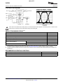
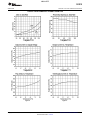
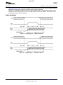
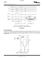
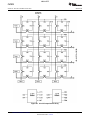
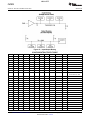
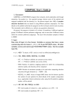
OBSOLETE
CLC018
www.ti.com
SNLS019C – MAY 2004 – REVISED AUGUST 2006
CLC018 8 x 8 Digital Crosspoint Switch, 1.485 Gbps
Check for Samples: CLC018
FEATURES
DESCRIPTION
•
The CLC018 is a fully differential 8x8 digital
crosspoint switch capable of operating at data rates
exceeding 1.485 Gbps per channel. Its non-blocking
architecture
utilizes
eight
independent
8:1
multiplexers to allow each output to be independently
connected to any input and any input to be connected
to any or all outputs. Additionally, each output can be
individually disabled and set to a high-impedance
state. This TRI-STATE feature allows flexible
expansion to larger switch array sizes.
1
2
•
•
•
•
•
•
•
Supports SMPTE 259M, SMPTE 344M, and
SMPTE 292M
Fully Differential Signal Path
Non-Blocking
Flexible Expansion to Larger Array Sizes with
Very Low Power
Single +5/−5V or Dual ±5V Operation
TRI-STATE Outputs
Double Row Latch Architecture
64-Lead QFP Package
APPLICATIONS
•
•
•
•
•
•
•
Routing Switchers
Production Switchers
Master Control Switchers
Telecom/Datacom Switchers
Storage Area Network (SAM)
Packet Switching
ATM SONET
KEY SPECIFICATIONS
•
•
•
•
High Speed: >1.485 Gbps
Low Jitter:
– <50 psPP for Rates <500 Mbps
– <100 psPP for Rates <1.485 Gbps
Low Power; 850 mW with all Outputs Active
Fast Output Edge Speeds: 250 ps
Low channel-to-channel crosstalk allows the CLC018
to provide superior all-hostile jitter of 50 psPP. This
excellent signal fidelity along with low power
consumption of 850 mW make the CLC018 ideal for
digital video switching plus a variety of data
communication and telecommunication applications.
The fully differential signal path provides excellent
noise immunity, and the I/Os support ECL and PECL
logic levels. In addition, the inputs may be driven
single-ended or differentially and accept a wide range
of common mode levels including the positive supply.
Single +5V or −5V supplies or dual +5V supplies are
supported. Dual supply mode allows the control
signals to be referenced to the positive supply (+5V)
while the high-speed I/O remains ECL compatible.
The double row latch architecture utilized in the
CLC018 allows switch reprogramming to occur in the
background during operation. Activation of the new
configuration occurs with a single “configure” pulse.
Data integrity and jitter performance on unchanged
outputs are maintained during reconfiguration. Two
reset modes are provided. Broadcast reset results in
all outputs being connected to input port DI0. TRISTATE Reset results in all outputs being disabled.
The CLC018 is fabricated on a high-performance
BiCMOS process and is available in a 64-lead plastic
quad flat pack (QFP).
1
2
Please be aware that an important notice concerning availability, standard warranty, and use in critical applications of
Texas Instruments semiconductor products and disclaimers thereto appears at the end of this data sheet.
All trademarks are the property of their respective owners.
PRODUCTION DATA information is current as of publication date.
Products conform to specifications per the terms of the Texas
Instruments standard warranty. Production processing does not
necessarily include testing of all parameters.
Copyright © 2004–2006, Texas Instruments Incorporated
OBSOLETE
CLC018
SNLS019C – MAY 2004 – REVISED AUGUST 2006
www.ti.com
CLC018 BLOCK DIAGRAM
These devices have limited built-in ESD protection. The leads should be shorted together or the device placed in conductive foam
during storage or handling to prevent electrostatic damage to the MOS gates.
ABSOLUTE MAXIMUM RATINGS (1) (2)
−0.3V to +6.0V
Supply Voltage (VCC–V EE)
VLL Maximum
VCC +6V
VCC −0.5V
VLL Minimum
−65°C to +150°C
Storage Temperature Range
Lead Temp. (Soldering 4 sec.)
+260°C
ESD Rating
Package Thermal Resistance
Reliability Information
(1)
(2)
TBD
θJA 64-Pin QFP
75°C/W
θJC 64-Pin QFP
15°C/W
Transistor Count
3000
Absolute Maximum Ratings are those values beyond which the safety of the device cannot be ensured. They are not meant to imply that
the devices should be operated at these limits. The table of Electrical Characteristics specifies conditions of device operation.
If Military/Aerospace specified devices are required, please contact the Texas Instruments Sales Office/Distributors for availability and
specifications.
RECOMMENDED OPERATING CONDITIONS
Supply Voltage (VCC–V EE)
4.5V to 5.5V
Operating Temperature
−40°C to +85°C
VLL
VCC or VCC +5V
2
Submit Documentation Feedback
Copyright © 2004–2006, Texas Instruments Incorporated
Product Folder Links: CLC018
OBSOLETE
CLC018
www.ti.com
SNLS019C – MAY 2004 – REVISED AUGUST 2006
ELECTRICAL CHARACTERISTICS
(VCC = 0V, VEE = −5V, VLL = 0V; unless otherwise specified) (1) .
Parameter
Typ
+25°C
Conditions
Min/Max
+25°C (2)
Min/Max
−40°C to
+85°C (2)
Units
DYNAMIC PERFORMANCE
Max. Data Rate/Channel (NRZ)
Channel Jitter
See
(3)
Data Rate <500 Mbps
(4)
Data Rate <1.485 Gbps (4)
Propagation Delay (input to output)
1.485
Gbps
50
psPP
100
psPP
0.75
ns
Propagation Delay Match
See
(5)
±200
ps
Output Rise/Fall Time
See
(6)
250
ps
Duty Cycle Distortion
See
(7)
10
ps
OA Bus to LOAD ↑ Setup Time (T1)
15
ns
LOAD ↓ to OA Bus Hold Time (T2)
0
ns
IA Bus, TRI to LOAD ↓ Setup Time (T3)
5
ns
LOAD ↓ to IA Bus, TRI Hold Time (T4)
5
ns
LOAD
10
ns
CNFG
CONTROL TIMING: CONFIGURATION (8)
Min Pulse Width: (T5)
10
ns
LOAD ↑ to CNFG ↑ Delay (T6)
0
ns
CNFG ↑ to Valid Delay (T7)
20
ns
CNFG ↑ to Output TRI-STATE Delay (T8)
20
ns
CNFG ↑ to Output Active Delay (T9)
70
ns
5
ns
RES ↓ to TRI Hold Time (T11)
5
ns
Min Pulse Width: RES (T12)
10
ns
RES ↑ to TRI-STATE Mode Delay (T13)
20
ns
RES ↑ to Broadcast Mode Delay (T14)
70
ns
CONTROL TIMING: RESET (9)
TRI to RES ↑ Setup Time (T10)
STATIC PERFORMANCE
Signal I/O:
Min Input Swing, Differential
(See
(10)
)
150
Input Voltage Range Lower Limit
−2
Input Voltage Range Upper Limit
0.4
Input Bias Current
(See
(10)
Output Current
(See
(10)
Output Voltage Swing
RLOAD = 75Ω
and
(11)
)
)
200
200
mVPP
V
V
1.5
0.4/3.1
0.3/3.8
µA/output
10.7
8.53/12.80
7.20/14.3
mA
800
640/960
540/1060
mV
Output Voltage Range Lower Limit
−2.5
V
Output Voltage Range Upper Limit
0
V
(1)
(2)
VLL and all VEE supply pins are bypassed with 0.01 µF ceramic capacitor.
Min/max ratings are based on product characterization and simulation. Individual parameters are tested as noted. Outgoing quality
levels are determined from tested parameters.
(3) Bit error rate less than 10−9 over 50% of the bit cell interval.
(4) Measured using a pseudo-random (2 23−1 pattern) binary sequence with all other channels active with an uncorrelated signal.
(5) Spread in propagation delays for all input/output combinations.
(6) Measured between the 20% and 80% levels of the waveform.
(7) Difference in propagation delay for output low-to-high vs. output high-to-low transition.
(8) Refer to the Configuration Timing Diagram.
(9) Refer to the Reset Timing Diagram.
(10) J-level spec. is 100% tested at +25°C.
(11) The bias current for high speed data input depends on the number of data outputs that are selecting that input.
Submit Documentation Feedback
Copyright © 2004–2006, Texas Instruments Incorporated
Product Folder Links: CLC018
3
OBSOLETE
CLC018
SNLS019C – MAY 2004 – REVISED AUGUST 2006
www.ti.com
ELECTRICAL CHARACTERISTICS (continued)
(VCC = 0V, VEE = −5V, VLL = 0V; unless otherwise specified)(1) .
Typ
+25°C
Min/Max
+25°C (2)
Min/Max
−40°C to
+85°C (2)
Units
)
−1
−0.5
−0.5
V
)
Parameter
Conditions
Control Inputs:
(See
(12)
Input Voltage - LOW V IL max
(See
(12)
−4
−4.5
−4.5
V
Input Voltage - HIGH V IH min
VLL = +5V (12)
4
4.5
4.5
V
Input Voltage - LOW V IL max
VLL = +5V (12)
1
0.5
0.5
V
Input Voltage - HIGH V IH min
(12)
Input Current - HIGH
VIH = VLL
Input Current - LOW
VIL = VLL −5V (12)
1
0.2/2.0
0.1/2.5
µA
−100
−200/10
−250/15
µA
157
127/202
119/217
mA
MISCELLANEOUS PERFORMANCE
VCC Supply Current
All Outputs Active (12) (13) (14)
(12)
VCC Supply Current
All Outputs TRI-STATE
7
3/11
2/12
mA
VLL Supply Current
VLL = 0V (12)
2.5
1.7/3.3
1.5/3.5
mA
VLL Supply Current
VLL = +5V (12)
7
mA
1.5
pF
2
pF
Input Capacitance
Output Capacitance
(12) J-level spec. is 100% tested at +25°C.
(13) The VCC supply current is a function of the number of active data outputs. IVCC 18*N + 7 mA where N is an integer from 0 to 8.
(14) IVEE = IVCC + I VLL.
4
Submit Documentation Feedback
Copyright © 2004–2006, Texas Instruments Incorporated
Product Folder Links: CLC018
OBSOLETE
CLC018
www.ti.com
SNLS019C – MAY 2004 – REVISED AUGUST 2006
TYPICAL PERFORMANCE CHARACTERISTICS
Figure 1.
Figure 2.
Figure 3.
Figure 4.
Figure 5.
Figure 6.
Submit Documentation Feedback
Copyright © 2004–2006, Texas Instruments Incorporated
Product Folder Links: CLC018
5
OBSOLETE
CLC018
SNLS019C – MAY 2004 – REVISED AUGUST 2006
www.ti.com
CONNECTION DIAGRAM
Figure 7. 64-Lead QFP- Top View
See Package Number NBH0064A
PIN DESCRIPTIONS
POWER PINS VCC is the most positive rail for the data path. When the data levels are ECL compatible, then VCC
should be connected to GND. For PECL data (+5V referenced ECL), VCC is connected to the +5V supply.
Please refer to the Device Operation section in this datasheet for recommendations on the bypassing and
ground/power plane requirements of this device.
VEE is the most negative rail for the data path. When the data levels are ECL compatible, then VEE is
connected to a −5.2V power supply. For PECL data (+5V referenced ECL), V EE is connected to GND.
VLL is the logic-level power supply. If the control signals are referenced to +5V, VLL is connected to a +5V
supply. If control signals are ECL compatible, VLL is connected to GND.
DATA INPUT PINS DI0 and DI0 through DI7 and D17 are the data input pins to the CLC018. Depending upon
how the Power pins are connected (please refer to the Power Pins section) the data may be either
differential ECL, or differential PECL. To drive the CLC018 inputs with a single-ended signal, please refer
to the section Using Single-Ended Data in the OPERATION section of this datasheet.
DATA OUTPUT PINS DO0 and DO0 through DO7 and DO7 are the data output pins of the CLC018. The
CLC018 outputs are differential current outputs which can be converted to ECL or PECL compatible
outputs through the use of load resistors. Please refer to the Output Interfacing paragraph in the
OPERATION section of this datasheet for more details.
CONTROL PINS IA2, IA1 and IA0 are the three bit input selection address bus. The input port to be addressed is
placed on this bus. IA2 is the Most Significant Bit (MSB). If input port 6 is to be addressed, IA2, IA1, IA0
should have 1, 1, 0 asserted on them. The IA bus should be driven with CMOS levels, if VLL is +5V. These
levels are thus +5V referenced (standard CMOS). If VLL is connected to GND, the input levels are
referenced to the −5V and GND supplies.
OA2, OA1 and OA0 are the output selection address bus. The output port selected by the OA bus is
connected to the input port selected on the IA bus when the data is loaded into the configuration registers.
OA2 is the MSB. If OA2, OA1, OA0 are set to 0, 0, 1; then output port 1 will be selected.
CS is an active-high chip select input. When CS is high, the RES, LOAD, and CNFG pins will be enabled.
LOAD is the latch control for the LOAD register. When LOAD is high, the load register is transparent.
Outputs follow the state of the IA bus, and are presented to the inputs of the Configuration register
selected by the OA bus. When LOAD is low, the outputs of the Load register are latched.
RES is the reset control of the configuration and load registers. A high-going pulse on the RES pin
programs the switch matrix to one of two possible states: with TRI low, all outputs are connected to input
#0; with TRI high, all outputs are put in TRI-STATE condition.
TRI will program the selected output to be in a high impedance or TRI-STATE condition. To place an
output in TRI-STATE, assert a logic-high level on the TRI input when the desired input and output
addresses are asserted on the respective address inputs and strobe the LOAD input as depicted in the
6
Submit Documentation Feedback
Copyright © 2004–2006, Texas Instruments Incorporated
Product Folder Links: CLC018
OBSOLETE
CLC018
www.ti.com
SNLS019C – MAY 2004 – REVISED AUGUST 2006
Configuration Truth Table. To enable an output, assert a logic-low level on the TRI input together with the
appropriate addresses and strobe the LOAD input as previously described.
CNFG is the configuration register latch control. When CNFG is high the Configuration register is made
transparent, and the switch matrix is set to the state loaded into the Load registers. When CNFG is low,
the state of the switch matrix is latched.
TIMING DIAGRAMS
Figure 8. Timing Diagram — TRI-STATE Reset
Figure 9. Timing Diagram — “Broadcast Reset”
Submit Documentation Feedback
Copyright © 2004–2006, Texas Instruments Incorporated
Product Folder Links: CLC018
7
OBSOLETE
CLC018
SNLS019C – MAY 2004 – REVISED AUGUST 2006
www.ti.com
Figure 10. Timing Diagram—Switch Configuration
OPERATION
INPUT INTERFACING
The inputs to the CLC018 are high impedance differential inputs (see the equivalent input circuit in Figure 11).
The CLC018 can be operated with either ECL or PECL (+5V referenced ECL), depending upon the power supply
connections. The inputs are differential and must both be within the range of VCC– 2V to VCC + 0.4V in order to
function properly.
Figure 11. Equivalent Input Circuit
8
Submit Documentation Feedback
Copyright © 2004–2006, Texas Instruments Incorporated
Product Folder Links: CLC018
OBSOLETE
CLC018
www.ti.com
SNLS019C – MAY 2004 – REVISED AUGUST 2006
SINGLE ENDED INPUTS
Differential inputs are the preferred method of providing data to the CLC018, however, there are times when the
only signal available is single ended. To use the CLC018 with a single ended input, the unused input pin needs
to be biased at a point higher than the low logic level, and lower than the high logic level. For best noise
performance, the middle of the range is best. For ECL signals this point is about 2 diode drops below ground. It
is possible to bias the unused input with a low-pass filtered version of the data, as shown in Figure 12. In some
coding schemes there are pathological patterns that result in long sequences with no data transitions. During
these patterns, the bias on the unused input will drift towards the other input reducing the noise immunity which
makes this scheme undesirable. The most robust solution for single ended inputs is to place a comparator with
hysteresis in front of the CLC018. Such a part is the MC10E1652. See Figure 13 for an example of how to hook
this up.
Figure 12. Single Ended Input to CLC018
Figure 13. Single Ended Input to CLC018
OUTPUT INTERFACING
The outputs of the CLC018 are differential, current source outputs. They can be converted to ECL compatible
levels with the use of resistive loads as shown in Figure 14. The output swings will have a similar temperature
coefficient to 10KECL if a 1N4148 diode is used to set VOH. For most commercial temperature range
applications, a 75Ω resistor can be used as shown in Figure 15. Many circuits with differential inputs, such as the
CLC016 Data Retimer With Automatic Rate Selection, do not require true ECL levels, so the load resistors can
be connected directly to the positive rail as shown in Figure 16.
Figure 14. Generating 10k ECL
Outputs
Figure 15. Generating ECL
Outputs
Figure 16. Connecting the
CLC018 to the CLC016
OUTPUT SIGNAL QUALITY
The output signal eye pattern shown in Figure 17 was acquired using an Agilent 86100A scope and 86112A plug
in along with a TEK P6330 3GHz differential probe. The differential signal was probed across the output pins of
the CLC018. 75 Ohm pull up resistor were used as shown in Figure 16. A PRBS23 pattern was driven through
the part, and the resulting eye pattern is shown in Figure 17. The eye pattern is affected by the HF roll-off of the
probe which degrades the output transition time and affects jitter. Even with this loading the CLC018 provides
excellent signal quality and low jitter at 1.485 Gbps. Note 150 ps/div and 250 mV/div.
Submit Documentation Feedback
Copyright © 2004–2006, Texas Instruments Incorporated
Product Folder Links: CLC018
9
OBSOLETE
CLC018
SNLS019C – MAY 2004 – REVISED AUGUST 2006
www.ti.com
Figure 17. 1.485 Gbps Eye Pattern
POWER SUPPLIES, GROUNDING AND BYPASSING
The CLC018 uses separate power supplies for control and data circuitry. Data circuitry is supplied via VCC and
control circuitry via VLL. Supply connection VEE, the negative-most supply, is the common return for both.
Connection details for the different powering modes is shown in Table 1.
Internal and external capacitances, normal and parasitic, must be charged and discharged with changes in
output voltage. Charging current depends upon the size of these capacitances and the rate of change of voltage.
At the fast transition times of the CLC016, small amounts of stray capacitance at outputs can produce large
output and supply transient currents. Controlling transient currents requires particular attention to minimizing
stray capacitances and to providing effective bypassing in the design. Good and effective bypassing consisting of
0.01 µF to 0.1 µF monolithic ceramic and 4.7 µF to 10 µF, 35V tantalum capacitors. These capacitors should be
placed as close to power pins as practical and tightly connected to the power plane sandwich using multiple vias.
Needless to say, multilayer board technology should be employed for the CLC018 and similar high-frequencycapability devices.
CONFIGURING THE SWITCH
The CLC018 can be configured so that any output may be independently connected to any input and any input
be connected to any or all outputs. Each output may be independently enabled or placed in a high-impedance
state.
Data controlling the switch matrix and output mode are stored in two ranks of eight, 4-bit registers, one register
per output. The three most-significant bits in each register identify the input to be connected to that output. The
least-significant bit controls whether the output is active or TRI-STATE. A particular register in the first rank, the
LOAD REGISTERS, is selected by a 3-bit word placed on the output address (OA) bus. Data to be written into
the load register, consisting of the 3-bit address of the input to be connected to that output and the output-enable
control bit, are placed on the input address (IA) bus. Input data is stored in the load registers at the low-to-high
transition of the LOAD input pin with chip-select (CS) high-true. The contents of the load registers are transferred
to the second rank of CONFIGURATION REGISTERS at the low-to-high transition of the CNFG input signal (with
CS high). This causes the state of the entire switch matrix to be set to the selected configuration.
The entire crosspoint may be placed in an initializing state, with all outputs connected to input-0 and with all
outputs either enabled or TRI-STATE. To do so, hold TRI low to make outputs active, or high to place outputs in
TRI-STATE, and apply a high-going pulse to the RES input pin (with CS high).
In summary, outputs are configured by:
a. First placing the 3-bit address of that output on the OA bus together with
b. The 3-bit address of the input to be connected to that output on the IA bus,
c. The output-enable (TRI-STATE) control bit for that output on the IA bus,
d. Making chip-select (CS) true, and then
e. Providing a high-going pulse to the LOAD input pin.
f. Repeat these four steps for each output to be configured.
The entire crosspoint matrix may now be configured with the data held in the load registers. To implement the
configuration, apply a high-going pulse to the CNFG input pin. The contents of the load registers are transferred
to the configuration registers and the new configuration of all crosspoints is effected.
10
Submit Documentation Feedback
Copyright © 2004–2006, Texas Instruments Incorporated
Product Folder Links: CLC018
OBSOLETE
CLC018
www.ti.com
SNLS019C – MAY 2004 – REVISED AUGUST 2006
The CLC018 Configuration Truth Table is shown at the end of the datasheet.
EXPANDING THE SWITCH SIZE
The CLC018 was designed for easy expansion to larger array sizes without paying a significant penalty in either
speed or power. The power dissipation of the expanded array will be dominated by the number of active outputs,
therefore power will increase linearly with the array size even though the number of components required
increases as the square of the array size. As an example, a single CLC018 can be used for an 8x8 array, and it
will dissipate about 0.85W. A 32 x 32 array will require 16 CLC018s and will consume only about 4W.
Table 1. Interfacing of the Power Supplies and Bypass Capacitors
Supply Operation
I/O Data Level
Control Signal Low/High
Single −5V
Single +5V
ECL
PECL
ECL
−5V/GND
GND/+5V
GND/+5V
1. Bypass each VEE supply with
a 0.01 µF capacitor. 2. Connect
VCC and VLL to the ground
plane. 3. A power plane isn't
required for VEE but can be
used.
1. Bypass each VCC supply with a
0.01 µF capacitor. 2. Bypass the
VLL supply with a 0.01 µF. 3.
Connect VEE to the ground plane. 4.
Use a +5V power plane for VCC.
1. Bypass each VEE supply with a
0.01 µF capacitor. 2. Bypass the
VLL supply with a 0.01 µF. 3.
Connect VCC to the ground
plane. 4. A power plane isn't
required for +5V (VLL) or −5V
(VEE) supplies. but can be used.
Dual ±5V
Connection
Key Information
EXPANDING THE NUMBER OF OUTPUT PORTS
To expand the number of output ports in a switch array, the inputs of multiple CLC018s are connected in parallel.
The bus used to connect the input ports should be a controlled impedance transmission line as shown in
Figure 18. To control the switch array, the IA, OA and TRI buses are all connected in parallel and a decoder is
used to assert high the CS of the CLC018 that is to be addressed. This is also shown in Figure 18.
Submit Documentation Feedback
Copyright © 2004–2006, Texas Instruments Incorporated
Product Folder Links: CLC018
11
OBSOLETE
CLC018
SNLS019C – MAY 2004 – REVISED AUGUST 2006
www.ti.com
Figure 18. 8 x 16 Crosspoint Example
EXPANDING THE NUMBER OF INPUT PORTS
Expanding the number of inputs in a switch array is accomplished by wire-ORing the outputs together, and TRISTATEing the outputs of the CLC018s that do not have their inputs selected. The output bus should be a
controlled impedance transmission line with proper termination. This is shown in Figure 19. The circuit uses a 1of-2 decoder with complemented outputs to control the TRI pins of the CLC018s in the array. Thus, all CLC018s
are programmed simultaneously, and all of them, except for the one with the selected input, are placed in the
TRI-STATE mode.
EXPANDING BOTH INPUTS AND OUTPUTS
To increase both the number of inputs and outputs in an array, apply both the input port and output port
expansion techniques simultaneously. In Figure 20, this is shown for the case of a 24 input by 32 output switch
array. Note that both input and output buses need to be controlled impedance transmission lines. The CS pins
for rows of CLC018s are connected together and become the row select inputs, whereas the TRI pins are
connected together for the columns of CLC018s and become the column select pins.
12
Submit Documentation Feedback
Copyright © 2004–2006, Texas Instruments Incorporated
Product Folder Links: CLC018
OBSOLETE
CLC018
www.ti.com
SNLS019C – MAY 2004 – REVISED AUGUST 2006
Figure 19. Expanded Input Ports
Submit Documentation Feedback
Copyright © 2004–2006, Texas Instruments Incorporated
Product Folder Links: CLC018
13
OBSOLETE
CLC018
SNLS019C – MAY 2004 – REVISED AUGUST 2006
www.ti.com
Figure 20. 24 x 32 Output Switch Array
14
Submit Documentation Feedback
Copyright © 2004–2006, Texas Instruments Incorporated
Product Folder Links: CLC018
OBSOLETE
CLC018
www.ti.com
SNLS019C – MAY 2004 – REVISED AUGUST 2006
CALCULATING THE POWER DISSIPATION IN AN EXPANDED ARRAY
The CLC016 dissipates about 100 mW per active output plus about 50 mW quiescent power. With all outputs
active, this is about 850 mW. In an expanded array, all devices will dissipate quiescent power, but only those
devices with active outputs will dissipate the 100 mW/output. So, an N-by-M device array (an 8×N-input-by-8×Moutput switch) with all outputs active will dissipate N × M × 50 mW + 8 × M × 100 mW. A 32-input × 32-output (4
× 4 device) switch array dissipates 4 × 4 × 50 mW + 8 × 4 × 100 mW = 4W.
CONTROLLED IMPEDANCE TRANSMISSION LINES AND OTHER LAYOUT TECHNIQUES
All transmission lines whose length is greater than ¼ wavelength of the highest frequencies present in the
transmitted signal require proper attention to impedance control to avoid distortion of the signal. Digital signals
are especially susceptible to distortion due to poorly controlled line characteristics and reflections. With its 250 ps
output transitions, which imply a bandwidth of 4 GHz or more, transmission lines driven by the CLC018 must be
carefully designed and correctly terminated. Either microstrip line, which resides on the outer surfaces of a
printed circuit board and paired with an image ground plane, or stripline, which is sandwiched in an inner layer
between image ground planes, may be used in CLC018 designs. With either line type, it is important to maintain
a uniform characteristic impedance over the entire extent of the transmission line system. Likewise, the receiving
end of these lines must be terminated in a resistance equal to the characteristic impedance to preserve signal
fidelity. Figure 21 shows representative methods of interfacing to and from the CLC018.
Often, when voltage-mode drivers, such as ECL, with low output impedance (also called equivalent generator
resistance) are used to drive bus networks, a series resistor connects the output of the amplifier to the
transmission line. This resistor serves both as a termination for any signals travelling toward the source- end of
the line and as the series leg of a voltage divider (with the transmission line as the shunt leg) to reduce the
transmitted signal level. This resistor's correct value is ZO − R OUT. However, a value equal to ZO may be used
successfully in most situations. The receiving end of the line is terminated in a resistance equal to the value of ZO
of the receiving end of the line. A resistance equal to the line's ZO works in most situations. In cases where the
bus is heavily loaded, the receiving end termination's value may need to be reduced to the loaded- ZO of the line.
(Please see the material on distributed loading effects on line characteristics in the Fairchild F100K ECL 300
Series Databook and Design Guide).
Current-mode drivers, with their high equivalent generator resistance, when used as bus drivers require a
resistance equal to Z O at each end of the bus to either power or ground as appropriate for the design.
A detailed discussion of digital transmission line design techniques is beyond the scope of this data sheet, but
many good references are available from Texas Instruments and others. Extensive material is available in the
Texas Instruments Interface Databook, the Fairchild F100K ECL 300 Series Databook and Design Guide and the
Motorola MECL System Design Handbook.
Especially useful is the Texas Instruments Transmission Line RAPIDESIGNER© Sliderule and user manual AN905 (SNLA035).
Submit Documentation Feedback
Copyright © 2004–2006, Texas Instruments Incorporated
Product Folder Links: CLC018
15
OBSOLETE
CLC018
SNLS019C – MAY 2004 – REVISED AUGUST 2006
www.ti.com
Figure 21. Input/Output Busing
CONFIGURATION TRUTH TABLE
16
IA2
IA1
IA0
OA2
OA1
OA0
TRI
RES
LOAD
CNFG
CS
X
X
X
X
X
X
X
X
X
X
0
NO CHANGE
X
X
X
X
X
X
0
X
X
1
Load I/P 0 to All O/Ps
X
X
X
X
X
X
1
X
X
1
TRI-STATE All O/P 0
X
X
X
0
0
0
1
0
0
1
TRI-STATE O/P 0
X
X
X
0
0
1
1
0
0
1
TRI-STATE O/P 1
X
X
X
0
1
0
1
0
0
1
TRI-STATE O/P 2
X
X
X
C
B
A
1
0
0
1
TRI-STATE O/P CBA
•
•
•
•
•
•
•
•
•
•
•
R
Q
P
C
B
A
0
0
0
1
Load I/P PQR to O/P CBA
and Enable O/P CBA
•
•
•
•
•
•
•
•
•
•
•
•
0
0
0
0
0
0
0
0
0
1
Load I/P 0 to O/P 0
0
0
0
0
0
1
0
0
0
1
Load I/P 0 to O/P 1
0
0
0
0
1
0
0
0
0
1
Load I/P 0 to O/P 2
0
0
0
0
1
1
0
0
0
1
Load I/P 0 to O/P 3
0
0
0
1
0
0
0
0
0
1
Load I/P 0 to O/P 4
0
0
0
1
0
1
0
0
0
1
Load I/P 0 to O/P 5
0
0
0
1
1
0
0
0
0
1
Load I/P 0 to O/P 6
0
0
0
1
1
1
0
0
0
1
Load I/P 0 to O/P 7
0
0
1
0
0
0
0
0
0
1
Load I/P 1 to O/P 0
0
0
1
0
0
1
0
0
0
1
Load I/P 1 to O/P 1
0
0
1
0
1
0
0
0
0
1
Load I/P 1 to O/P 2
0
0
1
0
1
1
0
0
0
1
Load I/P 1 to O/P 3
•
•
•
•
•
•
•
•
•
•
•
0
0
1
1
1
1
0
0
0
1
Load I/P 1 to O/P 7
•
•
•
•
•
•
•
•
1
1
1
1
1
0
0
0
•
Condition of Device
•
•
Submit Documentation Feedback
•
•
•
0
1
Load I/P 7 to O/P 6
Copyright © 2004–2006, Texas Instruments Incorporated
Product Folder Links: CLC018
OBSOLETE
CLC018
www.ti.com
SNLS019C – MAY 2004 – REVISED AUGUST 2006
CONFIGURATION TRUTH TABLE (continued)
1
1
1
1
1
1
0
0
X
X
X
X
X
X
X
0
0
0
1
Load I/P 7 to O/P 7
1
Activate New
Configuration
Submit Documentation Feedback
Copyright © 2004–2006, Texas Instruments Incorporated
Product Folder Links: CLC018
17
IMPORTANT NOTICE
Texas Instruments Incorporated and its subsidiaries (TI) reserve the right to make corrections, enhancements, improvements and other
changes to its semiconductor products and services per JESD46, latest issue, and to discontinue any product or service per JESD48, latest
issue. Buyers should obtain the latest relevant information before placing orders and should verify that such information is current and
complete. All semiconductor products (also referred to herein as “components”) are sold subject to TI’s terms and conditions of sale
supplied at the time of order acknowledgment.
TI warrants performance of its components to the specifications applicable at the time of sale, in accordance with the warranty in TI’s terms
and conditions of sale of semiconductor products. Testing and other quality control techniques are used to the extent TI deems necessary
to support this warranty. Except where mandated by applicable law, testing of all parameters of each component is not necessarily
performed.
TI assumes no liability for applications assistance or the design of Buyers’ products. Buyers are responsible for their products and
applications using TI components. To minimize the risks associated with Buyers’ products and applications, Buyers should provide
adequate design and operating safeguards.
TI does not warrant or represent that any license, either express or implied, is granted under any patent right, copyright, mask work right, or
other intellectual property right relating to any combination, machine, or process in which TI components or services are used. Information
published by TI regarding third-party products or services does not constitute a license to use such products or services or a warranty or
endorsement thereof. Use of such information may require a license from a third party under the patents or other intellectual property of the
third party, or a license from TI under the patents or other intellectual property of TI.
Reproduction of significant portions of TI information in TI data books or data sheets is permissible only if reproduction is without alteration
and is accompanied by all associated warranties, conditions, limitations, and notices. TI is not responsible or liable for such altered
documentation. Information of third parties may be subject to additional restrictions.
Resale of TI components or services with statements different from or beyond the parameters stated by TI for that component or service
voids all express and any implied warranties for the associated TI component or service and is an unfair and deceptive business practice.
TI is not responsible or liable for any such statements.
Buyer acknowledges and agrees that it is solely responsible for compliance with all legal, regulatory and safety-related requirements
concerning its products, and any use of TI components in its applications, notwithstanding any applications-related information or support
that may be provided by TI. Buyer represents and agrees that it has all the necessary expertise to create and implement safeguards which
anticipate dangerous consequences of failures, monitor failures and their consequences, lessen the likelihood of failures that might cause
harm and take appropriate remedial actions. Buyer will fully indemnify TI and its representatives against any damages arising out of the use
of any TI components in safety-critical applications.
In some cases, TI components may be promoted specifically to facilitate safety-related applications. With such components, TI’s goal is to
help enable customers to design and create their own end-product solutions that meet applicable functional safety standards and
requirements. Nonetheless, such components are subject to these terms.
No TI components are authorized for use in FDA Class III (or similar life-critical medical equipment) unless authorized officers of the parties
have executed a special agreement specifically governing such use.
Only those TI components which TI has specifically designated as military grade or “enhanced plastic” are designed and intended for use in
military/aerospace applications or environments. Buyer acknowledges and agrees that any military or aerospace use of TI components
which have not been so designated is solely at the Buyer's risk, and that Buyer is solely responsible for compliance with all legal and
regulatory requirements in connection with such use.
TI has specifically designated certain components as meeting ISO/TS16949 requirements, mainly for automotive use. In any case of use of
non-designated products, TI will not be responsible for any failure to meet ISO/TS16949.
Products
Applications
Audio
www.ti.com/audio
Automotive and Transportation
www.ti.com/automotive
Amplifiers
amplifier.ti.com
Communications and Telecom
www.ti.com/communications
Data Converters
dataconverter.ti.com
Computers and Peripherals
www.ti.com/computers
DLP® Products
www.dlp.com
Consumer Electronics
www.ti.com/consumer-apps
DSP
dsp.ti.com
Energy and Lighting
www.ti.com/energy
Clocks and Timers
www.ti.com/clocks
Industrial
www.ti.com/industrial
Interface
interface.ti.com
Medical
www.ti.com/medical
Logic
logic.ti.com
Security
www.ti.com/security
Power Mgmt
power.ti.com
Space, Avionics and Defense
www.ti.com/space-avionics-defense
Microcontrollers
microcontroller.ti.com
Video and Imaging
www.ti.com/video
RFID
www.ti-rfid.com
OMAP Applications Processors
www.ti.com/omap
TI E2E Community
e2e.ti.com
Wireless Connectivity
www.ti.com/wirelessconnectivity
Mailing Address: Texas Instruments, Post Office Box 655303, Dallas, Texas 75265
Copyright © 2013, Texas Instruments Incorporated