1
THE INTRODUCTION OF
HITACHI H8 MICROCOMPUTERS
The company names and product names contained in this manual are trademarks or registered
trademarks. The web site addresses (URLs) mentioned in this manual were confirmed to be valid
as of November 2000.
The copyright of this manual is protected by the copyright laws. Reproducing, duplicating by using,
for example, a copy machine, or inputting to electronic equipment the whole or part of this manual
without permission may infringe on the copyright laws.
Duplication of this manual is prohibited, except for the exceptions defined in the copyright laws. To
request permission to duplicate the contents of this manual, please obtain permission from the
Japan Reprographic Rights Center.
Some useful contact details are given below. We recommend contacting them by letter or fax.
Japan Reprographic Rights Center
Tel: +81-3-3401-2382
Fax: +81-3-3401-2386
3-3-7, Kita-aoyama, Minato-ku, Tokyo 107-0061
Dai-ichi Aoyama Building, 3F
Ohmsha, Ltd.
Dept. responsible for the copyright laws
Tel: +81-3-3233-0641
Fax: +81-3-3293-0641
3-3-7, Kanda-nishiki-cho, Chiyoda-ku, Tokyo 101-8460
Cautions
1. Hitachi neither warrants nor grants licenses of any rights of Hitachi’s or any third party’s
patent, copyright, trademark, or other intellectual property rights for information contained in
this document. Hitachi bears no responsibility for problems that may arise with third party’s
rights, including intellectual property rights, in connection with use of the information
contained in this document.
2. Products and product specifications may be subject to change without notice. Confirm that you
have received the latest product standards or specifications before final design, purchase or
use.
3. Hitachi makes every attempt to ensure that its products are of high quality and reliability.
However, contact Hitachi’s sales office before using the product in an application that
demands especially high quality and reliability or where its failure or malfunction may directly
threaten human life or cause risk of bodily injury, such as aerospace, aeronautics, nuclear
power, combustion control, transportation, traffic, safety equipment or medical equipment for
life support.
4. Design your application so that the product is used within the ranges guaranteed by Hitachi
particularly for maximum rating, operating supply voltage range, heat radiation characteristics,
installation conditions and other characteristics. Hitachi bears no responsibility for failure or
damage when used beyond the guaranteed ranges. Even within the guaranteed ranges,
consider normally foreseeable failure rates or failure modes in semiconductor devices and
employ systemic measures such as fail-safes, so that the equipment incorporating Hitachi
product does not cause bodily injury, fire or other consequential damage due to operation of
the Hitachi product.
5. This product is not designed to be radiation resistant.
6. No one is permitted to reproduce or duplicate, in any form, the whole or part of this document
without written approval from Hitachi.
7. Contact Hitachi’s sales office for any questions regarding this document or Hitachi
semiconductor products.
Copyrights and liability
The programs included on this CD-ROM are for evaluation purposes only, and may be used free
of charge. The copyrights for these programs belong to Hitachi, Ltd., and to the authors of the
programs. These programs may not be reproduced or distributed in any part, or in their entirety.
The sample programs are intended to introduce the functions of the H8/3048F, and operation is
not guaranteed. Ohmsha Ltd. and the authors of these programs assume no responsibility for any
problems caused by using the programs contained in this manual or on the CD-ROM.
Preface
Nowadays, people are supported by computers in many ways in their everyday lives. Personal
computers are one type of computer, perhaps the type with which people are most familiar. A
personal computer has a computer inside it, and can be used to access the Internet and for many
other purposes. The name of this internal computer is rarely noted, but it is used to run and control
personal computers and many other computerized devices. This is called an “embedded”
computer. Unlike a personal computer, its programs are not available on hard disks or CD-ROMs,
and cannot be edited by users. It always runs using the same programs, and is used in countless
applications, among them cellular telephones, facsimile machines, printers, washing machines,
refrigerators, microwave ovens, computer game machines, automotive engines, air conditioners,
and meters, to name just a few. Nearly all of these embedded computers are microcomputers that
are marketed in chip form. The H8 by Hitachi that is discussed in this manual is a representative
type of microcomputer.
As long as the hardware is available in some finished form and programs have been installed,
personal computers can do just about anything we want them to do. The same applies to
microcomputers. As long as a chip has been installed, they can do almost anything. Because there
are no restrictions in terms of an operating system and hardware, like those that apply to personal
computers, microcomputers offer outstanding flexibility.
Numerous companies use microcomputers for system development of products, and countless
numbers of engineers are using microcomputers in their work. Not many school curricula cover
microcomputers, however, and most people who know anything about microcomputers learn it
through educational programs at work.
When microcomputers first appeared on the scene, in the 1970s and 1980s, many introductory
texts were available, and I had access to a wealth of documentation concerning products such as
the Z80 and MC6800. It was an ideal period for beginners to delve into the world of
microcomputers. Nowadays, however, even though microcomputers are in common use, most
textbooks assume that the reader has already acquired a fundamental knowledge of them, and it
has become rather difficult to find good information at the introductory level.
This manual was designed for future engineers in mind, and explains how microcomputers are
used, based on the H8 as an example. The instructions and signal terminal operation vary from one
product to another, but the basic approach to microcomputers is largely the same. The basic
material that you learn in this book through using the H8 can be applied to other microcomputers
as well.
What is important is how you use the tools you will learn here. Using the H8 as an example, this
book will teach you how to use a microcomputer. We hope you will then use that knowledge as a
springboard to devising applications of your own. Japan has a strong reputation for engineering
and technology, and microcomputers are a very important and valuable part of that technology. By
i
designing products using microcomputers, you will experience the pleasure of developing new
products, and come to realize how important that process can be.
We hope that this book will provide you with a thorough and instructional introduction to
microcomputers.
Finally, I would like to express my appreciation to Mr. Masuda, the Senior Engineer of the System
LSI Business Division at Hitachi, Ltd., who kindly provided me with the assembler and C
compiler used to develop the H8 microcomputer when this book was published, and to Mr.
Toyoshima, the Team Leader at Hitachi Kodaira Semiconductor Co., Ltd., who provided me with
information as a member of the Micom Car Rally Office.
November 2000
Yukiho Fujisawa
ii
Contents
Chapter 1 What Is a Microcomputer?................................................................1
1.1
1.2
1.3
Microcomputers in Our Everyday Lives........................................................................... 2
How do Microcomputers Work?....................................................................................... 9
1.2.1 What the Microcomputer does............................................................................. 9
1.2.2 Elements other than the Microcomputer (CPU)................................................... 10
1.2.3 Types of Microcomputers .................................................................................... 14
Memory Data and Binary Values...................................................................................... 16
1.3.1 Instructions and Binary Values ............................................................................ 17
1.3.2 Numeric Expressions ........................................................................................... 17
1.3.3 Character Codes ................................................................................................... 21
1.3.4 Decimal Point Data .............................................................................................. 21
1.3.5 Expressing Numeric Values................................................................................. 22
1.3.6 Memory Maps...................................................................................................... 22
Chapter 2 H8 Microcomputers have High-Levels of Performance and
Functionality ....................................................................................25
2.1
2.2
2.3
What is an H8 Microcomputer? ........................................................................................ 25
Operation Mode of the H8/3048F ..................................................................................... 27
2.2.1 Summary.............................................................................................................. 27
2.2.2 Single Chip .......................................................................................................... 30
2.2.3 Memory Expansion.............................................................................................. 32
Configuration of Registers and Programming .................................................................. 34
2.3.1 Register Configuration......................................................................................... 34
2.3.2 Instruction ............................................................................................................ 40
2.3.3 Programming ....................................................................................................... 53
2.3.4 Size of the Memory and Performance in Executing an Instruction...................... 70
2.3.5 Basic Input and Output ........................................................................................ 75
Chapter 3 Reset and Interrupts...........................................................................93
3.1
3.2
Writing Programs to ROM................................................................................................ 93
3.1.1 Hardware.............................................................................................................. 93
3.1.2 Programs .............................................................................................................. 94
3.1.3 Further Premised Hardware ................................................................................. 95
Interrupts ........................................................................................................................... 101
3.2.1 Need for Interrupt Functions................................................................................ 101
3.2.2 Operation on Occurrence of an Interrupt ............................................................. 102
3.2.3 Example of Interrupt Use..................................................................................... 105
iii
Chapter 4 Internal Peripheral Functions The functions and how to use them
(circuits and programs)....................................................................111
4.1
4.2
4.3
4.4
4.5
4.6
A/D Converters ................................................................................................................. 112
4.1.1 Overview of the A/D Converter........................................................................... 112
4.1.2 Example of How the A/D Converter is Used....................................................... 116
4.1.3 A/D Conversion Completed Interrupt.................................................................. 118
D/A Converter................................................................................................................... 122
4.2.1 An Overview of the D/A Converter ..................................................................... 122
4.2.2 Example of How the D/A Converter is Used....................................................... 124
16-Bit Timer (ITU) ........................................................................................................... 126
4.3.1 Overview of the ITU............................................................................................ 126
4.3.2 Example Using the Interval Timer....................................................................... 130
4.3.3 Example of Using Toggle Output ........................................................................ 138
Serial Communication (SCI)............................................................................................. 140
4.4.1 Overview of the SCI ............................................................................................ 141
4.4.2 Example Using Start-Stop Synchronized Communication .................................. 142
4.4.3 Example Using Clock Synchronization Communication..................................... 151
DMA Controller................................................................................................................ 154
4.5.1 Various Ways of Sending Data............................................................................ 154
4.5.2 Overview of the DMAC....................................................................................... 157
4.5.3 Example Using the Full Address Mode ............................................................... 158
4.5.4 Example Using the Short Address Mode ............................................................. 165
WDT ................................................................................................................................. 169
4.6.1 Overview of the WDT ......................................................................................... 169
4.6.2 Program Example Showing Reset Using the WDT ............................................. 171
4.6.3 Example Using an Interval Timer through the WDT........................................... 174
Chapter 5 PROGRAMMING IN THE C LANGUAGE ...................................177
5.1
5.2
5.3
5.4
iv
The C Language and the H8 Microcomputer.................................................................... 177
5.1.1 Standard I/O......................................................................................................... 178
5.1.2 Variable Sizes ...................................................................................................... 178
Tasks Prior to Calling main .............................................................................................. 179
5.2.1 Reset Processing .................................................................................................. 180
5.2.2 Initialization of Variables .................................................................................... 181
Peripheral Function Programming .................................................................................... 185
5.3.1 Register Access.................................................................................................... 186
5.3.2 Interrupt Processing ............................................................................................. 187
Basics of the C Language.................................................................................................. 191
5.4.1 Operators.............................................................................................................. 191
5.4.2 Control Statements............................................................................................... 191
5.4.3 Features of Structures, Arrays, and Pointers ........................................................ 199
5.4.4 Function Calls ...................................................................................................... 200
5.4.5 Declarations and Storage Classes......................................................................... 201
Chapter 6 EXTERNAL MEMORY INTERFACE............................................203
6.1
6.2
Memory Interface.............................................................................................................. 203
6.1.1 Basics of Memory Connection............................................................................. 204
6.1.2 Memory Interface Design .................................................................................... 208
6.1.3 DRAM Interface .................................................................................................. 217
6.1.4 Example of Application of the Refresh Timer as an Interval Timer.................... 224
Peripheral Function Interface............................................................................................ 225
6.2.1 Port Expansion..................................................................................................... 225
6.2.2 LCD Connection .................................................................................................. 226
Chapter 7 Using Applications More Effectively ...............................................229
7.1
7.2
7.3
7.4
7.5
Electronic organ: Using the timer to turn on the piezoelectric sounder ............................ 230
Motor Control 1: Timers can be used to run stepping motors........................................... 237
Motor Control 2: DC motor control is no problem with an encoder................................. 249
Digital Recording and Playback: timed recording is a simple function ............................ 253
Voice Processing: Going for the best possible vocal sound.............................................. 257
APPENDIX that Comes with This Manual .........................................................259
v
vi
Chapter 1 What Is a Microcomputer?
Let’s start off by defining a microcomputer. “Micro”, of course, refers to something small and
compact, while a computer can be defined as a kind of calculator that uses semiconductors and
other electronic components to carry out all kinds of computations. Actually, the first
microcomputers were used in compact calculators. The world’s first microcomputer was made in
the U.S., by Intel, and was called the “i4004”. Its first application was in a calculator. If you think
about how a calculator works, you press keys to enter numeric values, right? This is the same way
that data is entered in a computer, using some kind of input device. The value of the input key is
displayed to indicate to the user that the value has been entered correctly. If you disassembled a
calculator, you would find that the keys and the display unit are not directly connected; there is a
microcomputer between them. The microcomputer decides, based on the key input, what should
be displayed, using instructions (this is called an “operation”). A group of instructions is called a
program. After the numeric value has been input, detailed operations can be carried out, such as
the various arithmetic operations, by the operation keys. So the microcomputer uses a program
that has been stored in it in advance to execute the functions of a calculator.
Because of price considerations, however, dedicated ICs are used nowadays in calculators, instead
of microcomputers.
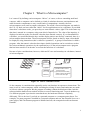
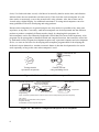
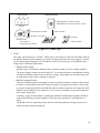
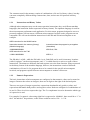
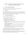
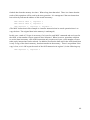
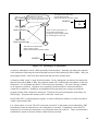
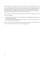
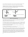
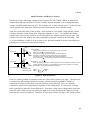
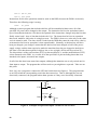
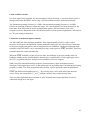
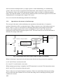
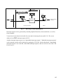
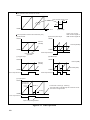
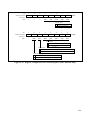
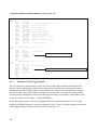
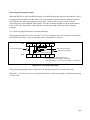
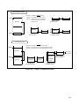
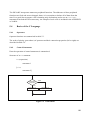
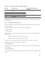
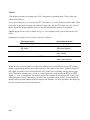
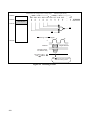
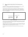
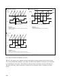
CPU
(operation unit)
Switch
Instructions
Memory
(1) Confirms whether a switch
has been pressed
(2) If pressed, shifts the existing
display to the left, and displays
the new value at the right.
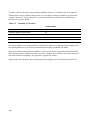
Figure 1.1 How a Calculator Works
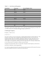
So the computer is a machine that repeatedly carries out functions in response to instructions. The
same is true of a microcomputer, which is nothing but a lump of stone (semiconductors are made
of silicon) without a program. But the program is nothing without the hardware either; both the
software and the hardware are needed in order to create a functioning unit. To put it another way,
if a different program is put into the same hardware, the hardware functions completely
differently. This is obvious if you look at a personal computer or a computer game player. For
example, if a game program is installed in a personal computer and run, the computer serves as a
game player, and if an Internet program is installed and run, the computer becomes an Internet
terminal.
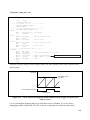
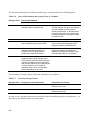
1
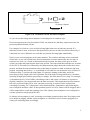
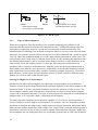
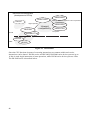
Memory in which
programs are stored
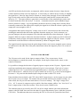
A
B
Figure 1.2 A microcomputer Integrates Hardware and Software
One good thing about computers is that they will do the same thing over and over without ever
complaining or making a mistake. They work whenever asked to, as long as the electricity that
serves as their fuel is supplied. Microcomputers function in our everyday lives now in far more
diverse capacities than just as calculators. They are working for us from the moment we get up
until the time we go to sleep, and even while we sleep. We can’t even imagine a life without
microcomputers, and yet we rarely stop to think about these machines that do so much for us.
Let’s look at how microcomputers are being used, and what they do for us.
1.1
Microcomputers in Our Everyday Lives
Most machines that we call information devices use microcomputers. Intel says in an
advertisement that microcomputers are the “heart” of the personal computer. Microcomputers are
crucial to the functioning of the personal computer. But they aren’t found just in personal
computers. Keyboards have their own separate microcomputers, while in notebook computers,
microcomputers control the power supply and battery. PDAs (Personal Digital Assistants), like
personal computers, use microcomputers. In response to instructions from the mouse and
keyboard, they run application programs, change screen displays, and carry out other functions.
Displaying the mouse cursor is another job the microcomputer does.
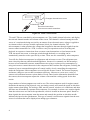
Computer game players work the same way as personal computers, although they use game pads
and, in some cases, bazooka guns instead of a mouse and keyboard. When you make a movement
on the game pad, the screen is constantly redrawn in rapid succession. Newer game players can
refresh the screen even faster than personal computers can.
2
Moves
the displayed
screen
Reads data from
a CD/DVD, etc.
Moved
Figure 1.3 How a Game Player Works
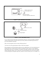
How often do you ever see the old, standard black telephone? Even the word “dial” is fast
becoming extinct, since no one ever “dials” a telephone anymore. Today’s telephones have
microcomputers that control answering machine, redialing and other functions. Facsimile
machines and cellular phones also use microcomputers. When you press a button on a telephone,
you hear a beeping sound, and the telephone number of the person you are calling is displayed on
the screen, along with the elapsed time and other information. Answering machines record and
play back messages. All of these functions are done using microcomputers.
Displays information/communicates with base station
Key is pressed
Figure 1.4 How a Cellular Phone Works
3
Changes channel/turns motor
Infrared rays
Receives instructions
from remote control transmitter
Figure 1.5 How a VTR Works
TVs and VTRs are controlled by microcomputers, too. They handle channel selection, and display
the selected channel number and volume on the screen. The channel is selected among the radio
waves of a certain node being received by an antenna. In an electronic tuner, voltage is applied to
an element called a varicap (variable capacitance) diode, for channel selection. The
microcomputer is what generates the voltage that is applied to the tuner through signals from the
remote control transmitter. In a VTR, in order to carry out operations such as recording and
playback in response to instructions from a remote control transmitter or from buttons on the
VTR, the motor has to turn, so that tape winds through the heads, or recording can be
automatically started at a time specified by a timer. These are also controlled by microcomputers.
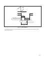
You will also find microcomputers in refrigerators and microwave ovens. The refrigerator uses
more electricity than any other household appliance, because it is constantly on. But nowadays,
because of environmental concerns, manufacturers are trying to reduce power consumption, by
using an inverter to control the motor in the compressor that circulates the refrigerant, reducing the
amount of power consumed through on/off control, and by closely controlling the temperature
inside the refrigerator. Microcomputers are used for this inverter control. The inverter frequency
and motor voltage are set to achieve maximum efficiency. Microwave ovens use a variety of
sensors to discriminate between various kinds of foods. Based on the information obtained from
the sensors, the microcomputer adjusts the volume of heat and the cooking speed for the best
results.
Large numbers of microcomputers are used in cars. The microcomputers used for engine control
determine the amount of fuel injected, carry out timing control, and control the speed at which the
engine rotates when idling. The air bags, ABS, traction control, windows, air conditioner and other
functions are all handled by separate microcomputers. For example, in newer cars, rotation signals
from the various axes are sent to the speedometer, which is located on the meter panel. Based on
these signals, the microcomputer turns the motor and controls the position at which the needle
indicates the speed on the speedometer. This type of control is used because signals from the axes
are not in a format that can be displayed on analog-type voltmeters.
4
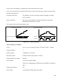
Menu
Displays optimum time
for microwave oven
Start
Confirms switches
Confirms temperature inside oven
Figure 1.6 How a Microwave Oven Works
40
20
60 80 100
6 8
120 4
2
km/H
RPM
These turn the motor
Micro
computer
Tire
Speed information
Engine speed
Engine
Figure 1.7 How a Speedometer Works
So, as we have seen up to this point, microcomputers function in a diverse spectrum of machines,
without needing people to run them, and carry out many functions automatically that make our
lives easier and more convenient.
Why are microcomputers used in so many different products?
The answer lies in the general-purpose nature of the microcomputer.
Microcomputers are used in the many products we have talked about so far, but certainly there are
products that don’t use them. When it comes to mechanical control, however, microcomputers
make things easier in a lot of situations. For instance, they make it possible to enter a time setting
simply by pressing a button. Also, it takes time to develop dedicated circuits, and if any mistakes
are made during the development stage, they cannot be corrected in many cases. For example, in a
5
clock, if a clockwork timer is used, a dial has to be turned by hand to set the time, and often the
indicated time does not match the real time exactly. If the clock has a microcomputer in it, the
time can be set accurately, even to the seconds unit, using a button. Also, the set time can be
viewed using a digital display, for additional reassurance. So using microcomputers can solve
many problems involved in developing and using products.
Because microcomputers are in general-purpose use, they make it is possible to buy same ones
anywhere, at any time. Conversely, same microcomputers can be incorporated into the different
product to produce completely different results, simply by changing their programs. So
microcomputers can be used instead of dedicated circuits that have been created separately. Also,
programs can be put together to handle difficult and complex functions, that cannot be carried out
by dedicated circuits. Program development requires only a personal computer and a development
device, so costs are far lower for developing microcomputer programs than for developing the
dedicated circuits themselves. Another economic feature is that the development device can be
used repeatedly as long as the same microcomputer is used.
Time can be set
precisely
4
3
2
1
0
SW
Liquid crystal
Precise time set
using oscillating circuit
Turning the dial
by hand is not precise
Figure 1.8 Mechanical Timer and Microcomputer Timer
Personal computer, etc.
ICE (in-circuit emulator)
Device that substitutes
for the microcomputer
Microcomputer
(Microcomputer is removed)
Completed!
Board being made
Programming
Input, conversion (combinations of 0s and 1s that can be interpreted by the microcomputer)
ICE control
Execution of one instruction in the program
Program aborting
Confirmation of microcomputer status
Figure 1.9 Mechanical Configuration Required for Development
6
(1) Switches are viewed
(2) Lamp is lighted
Takes time
Figure 1.10 Dedicated Circuit and Microcomputer
So you can see that using microcomputers is advantageous in countless ways.
Do microcomputers have any drawbacks? Well, one drawback is that they require more time for
processing than dedicated circuits.
For example, let’s look at a case in which a lamp lights when two switches are pressed. If a
dedicated circuit is used, as shown in the figure below, the two switches work most effectively if
connected in a series. When the two switches are pressed, the lamp lights immediately.
Now let’s use a microcomputer in the same situation. The switches and lamp are not connected
electrically. As we will explain later, the microcomputer executes instructions one at a time, in
response to a clock. As a result of instructions being executed, the lamp switch goes on if the
system can judge that both switches have been pressed. The instruction that reads the two switches
to the CPU is executed first, followed by the instruction that judges that both switches have been
pressed, and then the instruction that turns on the lamp in response to both switches having been
pressed. Assuming that it takes 1 µs (a millionth of a second) for one instruction to be executed, it
will take at least 3 µs before the lamp lights. If a person is turning on the lamp, and if the
processing is fairly simple, this is not a problem, but if the lamp is being turned on by a machine
operating at high speed, and the processing is complex, this time interval is too long. For example,
a calculation speed of 18.432 MHz (calculating at 640 x 480 pixels x 60 frames) is required to
digitally compress video images and store the data in memory. That means that one data element
has to be processed within 54 ns. Also, intricate processing is required for the compression,
consisting of queuing, DCT (dispersion cosine transformation), quantization, and producing the
sum of disparate absolute values. If the operation speed is too slow, frames will be dropped, and it
will be impossible to watch the resulting video. The ordinary microcomputer is not configured to
execute operations at high speed like this.
So when a microcomputer is used, executing even simple operations takes time. Developers need
to be skilled at judging whether a microcomputer or a dedicated circuit is better equipped for a
certain job, and using them accordingly.
7
Another option is to use a personal computer to put together a program and control various
devices. In this case, however, a board has to be incorporated into the personal computer so that
the device and the personal computer can be connected, and a standard interface has to be
processed and connected for the personal computer. The personal computer itself is fairly large, so
it cannot be incorporated into very many devices. Also, even though computers are less expensive
than they used to be, they are still comparatively high-priced, and although they offer
sophisticated processing capabilities, it is hardly feasible to incorporate one into, for example, a
refrigerator. Personal computers are restricted to certain applications for which they are well fitted.
So we will focus, rather than on personal computers, on microcomputers, which can easily be
incorporated into other devices. Of course, since microcomputers are used in personal computers,
we will also be learning about the inside of the personal computer as we proceed.
personal computer
No matter how small, a personal computer
will never fit inside a cellular phone.
Figure 1.11 Personal Computers and Microcomputers that can Fit into Other Devices
8
1.2
How do Microcomputers Work?
Microcomputers make our everyday lives easier and more convenient. Being able to use
microcomputers flexibly means various devices can be automated and new products can be
created. Before we can accomplish these aims, however, we need to know something about
microcomputers.
Let’s look at what goes inside a computer.
1.2.1
What the Microcomputer does
Unlike people, computers can’t think and act on their own. Combinations of instructions put
together ahead of time (programs) are retrieved one by one from a storage device (memory) and
operations executed based on those instructions.
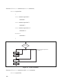
Let’s assume that, as shown in the figure, instructions have been stored in the memory (we’ll talk
later about how the instructions get stored in the memory). The first instruction is “Read data from
switch”. The computer specifies the place in the memory in which this instruction has been stored,
and reads the instruction. Next, the instruction that has been read is interpreted, and the data is
read from the location where the switch exists. This completes the operation of one instruction.
The microcomputer then reads the next instruction from the memory. This instruction says,
“Confirm whether switch is on”, so the data read in response to the previous instruction is
confirmed at this point. The next instruction says, “If the switch is on, proceed to next instruction,
and if not, return to switch reading instruction.”
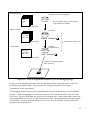
Microcomputer
Instruction 1 Read from switch
Reads instruction 1
(1) Fetch
Instruction 2 Is switch on?
If on, go to next; if off,
Instruction 3
go to instruction 1
Interprets instruction
(2) Decodes
Executes (3)
Switch information
Figure 1.12 Relationship between the Microcomputer and the Memory
In this way, the computer reads instructions from the memory and executes them. This operation is
summarized below.
9
Reading Instructions (Instruction Fetch)
The computer outputs an address that specifies where an instruction has been stored, and reads the
instruction from the memory.
Interpreting the Instruction (Instruction Decode)
The instruction that has been read is decoded.
The computer cannot understand the instruction without decoding it.
Executing the Instruction (Instruction Execute)
The decoded instruction is executed.
Fetching, decoding, and executing the instruction comprises one cycle of operation. This cycle is
then repeated for the next instruction, and then the one after that, and so on.
Copying, arithmetic operations, comparisons, logical operations and other processing can only be
carried out on one computer instruction at a time. Instructions can be put together in combinations,
however, to enable complex processing to be executed.
The computer can only execute one instruction at a time. Execution of instructions proceeds based
on a clock. The higher the clock frequency, the shorter the execution time.
(Instructions are stored in the memory ahead of time. This type of computer is called a
“Neumann” computer, based on the name of the person who developed it. Most computers
nowadays use this method.)
1.2.2
Elements other than the Microcomputer (CPU)
The storage device is called a memory. Instructions and data are stored in the memory in binary
format. In order to retrieve this stored information, the microcomputer assigns addresses to the
locations in which the instructions are stored, and uses these addresses to control the instructions.
In order to fetch an instruction, the microcomputer must know the address in which it is stored.
The memory provides the information stored at various addresses (without knowing whether it
consists of instructions or other information) to the microcomputer.
The terminal to which the microcomputer outputs addresses is called an address bus. This refers to
a group of bus signals that handle address information.
The terminal that reads instructions is called a data bus. The data bus is also used to fetch
instructions, but depending on the instruction, it can also be used to move data.
10
In order to incorporate the microcomputer into a product and use it as part of a system, we need a
signal bus that connects the memory, input/output circuits, and various other elements configuring
the system. Let’s look here at these other configuration elements.
If the computer system were a human being, the CPU (Central Processing Unit) would be the
brain. We also have a memory in the brain, right? The microcomputer system also has a memory,
that plays an equivalent role. There are various types of memories which are used for various
applications.
Memories can be divided into two general categories, based on their function.
One is the ROM (Read Only Memory), and the other is the RAM (Random Access Memory).
• ROM
The ROM is used only for reading. But in order to read data, it has to first have been stored in
the memory, a process called “writing” or “programming”. A special technique is used to write
data to the ROM. Data cannot be written directly to the ROM by the microcomputer. A
number of products are available for this purpose, with different products being used for
different applications. Data written to the ROM will be retained even if the power is turned off.
Masked ROM
In semiconductor manufacturing, 0s and 1s are stored in the ROM. One advantage is that,
when these are manufactured in large volumes, the cost drops. You are probably familiar
with this type because it is used in game cassettes.
Masked ROMs are all the same up to the stage when the transistor that serves as its base is
created. After that, transistors are created so that the wiring is different, or even if the
wiring is the same, the characteristics can be changed using 0s and 1s. Data is stored in the
memory in this way. The masked ROM is a type of ROM in which, once data has been
written, it cannot be rewritten.
EPROM (Erasable and Programmable ROM) or OTPROM (One Time Programmable
ROM)
The EPROM is a ROM that can be erased, while the OTPROM is a ROM to which data
can only be written once. The same chip is used for both, but the difference is whether or
not the package has a glass window. If it has a glass window, ultraviolet rays can pass
through the window to erase the data that has been stored. If there is no window, the data
cannot be erased. With EPROMs, data can be erased and programmed repeatedly, up to
100 times.
Special programming devices are used to write data to both. Because data can be erased
from EPROMs, these are used as the ROM when incomplete programs are being debugged,
or when the product is not being produced in large quantities.
EEPROM (Electrically Erasable and Programmable ROM)
This type of ROM can be electrically erased.
11
Unlike EPROMs, ultraviolet rays are not used, so the data can be rewritten with the
EEPROM mounted on the PCB.
EEPROMS can be reused anywhere from 100,000 to one million times, and are used
instead of IC cards or EPROMs/OTPROMs.
Flash Memory
Like the EEPROM, the flash memory can be electrically rewritten. It is different from the
EEPROM in that data cannot be rewritten in single-address units. Normally, it is
configured of blocks, each of which consists of between several kilobytes and several tens
of kilobytes of data, and these blocks are flashed (erased) individually to enable
information to be written. Previous information has to be deleted before new information
can be written to this type of ROM.
Flash memories can be further subdivided into OR/NOR and AND/NAND flash memories,
with OR/NOR being used in place of EPROM, OTPROM, and EEPROM memories.
Contents stored in the memory can be accessed directly, by specifying the address.
AND/NAND flash memories are used in digital cameras and MP3 players, and take the
place of a hard disk or floppy disk. With AND/NAND flash memories, when an address is
input, data is read and written serially in units of one sector (512 or 1024 bytes). This type
of memory works the same way as a cassette tape, and the target data can only be retrieved
by going through the data in sequential order. Programs cannot be stored to or directly read
from this type of memory.
Writing data this way requires a device called a ROM writer, and can be a time-consuming
process, as it is a more complex operation than reading data. All of the memory types
described above are grouped under the general name of “ROM”. One advantage of ROM is
that the contents stored in the memory are not lost when the power supply is turned off.
That’s why this type of memory is used in microcomputer systems to store the first
program that is run when the power supply is turned on, and to store fixed data that does
not change. It is an essential memory in such systems.
12
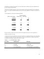
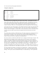
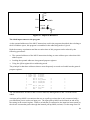
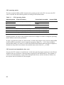
EPROM/OTPROM
Masked ROM
EPROMs have a window in them.
OTPROMs do not have a window in them.
Factory
}
}
Transistors are created
Data is written
Wiring is connected
UV lamp
Si wafer mask
Data is erased.
(This shape is
transferred to the wafer.)
Figure 1.13 ROM Types
• RAM
The other type of memory is “RAM”, which can be used freely to read and write data. Most of
the RAMs currently on the market are volatile, meaning that when the power supply is turned
off, the information disappears. This RAM also comes in several types, with different types
being used for different applications.
SRAM (Static RAM)
With this type of RAM, the contents can be retained as long as power is being supplied.
The power supply voltage can be lowered to 2 V to reduce the power consumption, and the
contents can still be retained even at this low voltage. This feature can be effectively used
in applications where battery backup is required.
DRAM (Dynamic RAM)
This type of RAM requires refreshing in order to retain the memory contents. Data cannot
be read or written while the RAM is being refreshed, so program execution is slower than
in systems using an SRAM, but the DRAM offers a memory capacity four times that of the
SRAM, and in addition is less expensive, so it is used as a memory in personal computers
and to store image data.
Currently, a type of RAM called a synchronous DRAM (Synchronous Dynamic RAM) is
used as the RAM in personal computers. With this type, operation is synchronized to a
clock.
The RAM is used to temporarily store data on which operations are being carried out, as
well as program status information.
13
SRAM
DRAM
Data stored simply
by turning on power supply
Data is written once again
(refreshed) before it is lost.
Figure 1.14 RAM Types
1.2.3
Types of Microcomputers
When microcomputers were first developed, the available technology only allowed 2,000
transistors that functioned as switches to be mounted on one IC. With all the changes that have
taken place in technology, however, we can now use more than 10 million transistors. The
miniaturization of technology has advanced to the point where we can now create tiny individual
transistors. For instance, around 1985 the wiring used to connect transistors had a width of around
2 µm. By 2000, that width had shrunk to 0.18 µm, approximately one-tenth its earlier value. The
current surface area is only about 1/100th the area required in 1985, meaning that transistors have
also shrunk proportionately, and we can now mount around 100 times as many transistors in the
same surface area as the number possible 15 years ago. More transistors means that more
operations can be carried out at the same time. Naturally, items are also being manufactured at
much smaller sizes than they were previously. Additionally, each individual transistor is much
more sophisticated and powerful, and is capable of operating at higher frequencies. Given all of
these advances, various types of microcomputers are now available, tailored to different usage
formats. Let’s look at some of the different types.
Striving for Higher-Level Performance
One direction in which microcomputers are advancing is towards higher-level performance.
Products are now being developed that boost the operation capability of the microcomputer to the
maximum limits. To do this, only those transistors required for operation circuits are used. The
microcomputer contains none of the memory elements that are required for the microcomputer
system, and no peripheral functions. This type of microcomputer is comprised of a combination of
multiple chips, so it is logically called a “multi-chip microcomputer”.
The multi-chip microcomputer has an operation capability of 32 to 64 bits, and incorporates a
variety of means to achieve high-level performance. For example, some are designed to perform
operations on multiple data items using a single instruction (Single Instruction Multi Data), while
others execute multiple instructions with a single clock (Super Scalar), and still others copy part of
the memory contents to a chip (Cache) in order to operate faster and more efficiently. Multi-chip
microcomputers are now being tailored for use in operating systems such as UNIX and Windows,
14
and are equipped with an MMU (Memory Management Unit) that lets a hard disk be used in place
of a memory when there is limited memory available.
Typical examples of such microcomputers are the Pentium, PowerPC, Strong-ARM, R10000, and
SuperH. These and others like them are used to achieve sophisticated mechanical control in
personal computers, workstations, network servers, sophisticated game players, and other devices.
Many of these microcomputers use a system called RISC (Reduced Instruction Set Computer).
With this system, the content handled by a single instruction is simplified, so that instructions can
be executed at a single clock. Because the instructions are simpler, internal circuits can also be
simplified. This makes the clock faster, so programs run faster. Currently, efforts are underway to
boost the clock speed to 1 GHz. Also, because the same results can be achieved even if the
instructions are executed in a different order, the execution time is not constant. Generally,
programming is done using the C language, and the execution order is left to the C compiler.
Striving for Smaller Sizes
Another direction in which development is moving is towards more compact sizes. Developers are
working to incorporate microcomputers into devices not only because of the convenience factor,
but also because it makes the device smaller and more portable, so that it has a smaller surface
area and volume. Microcomputers are thus used in applications where outstanding operation
performance is not required. For example, microcomputers used in devices such as small-scale
hot-water heaters and electric cooking pots do not need to be terribly sophisticated in terms of
operation capability. They simply view information from a temperature sensor and turn on the
heater if the temperature has dropped. The volume of information for the temperature sensor
doesn’t go much beyond 100 degrees, and control does not need to be implemented in singledegree units, so four bits are quite sufficient for this type of application. A time period of around
0.1 seconds is also fast enough to judge the temperature, since at that speed, the temperature
display appears to the user to be changing rapidly. A time frame of 0.1 seconds converted to a
frequency would be 10 Hz, and microcomputers are quite capable of processing information at
that rate. If the microcomputer were to be incorporated into the pot, however, we would need a
temperature sensor, and perhaps a temperature display as well. The temperature sensor and display
element themselves cannot be integrated on the same chip as the microcomputer, but the
peripheral functions that connect these to the CPU can be mounted on the same chip. Given this
circumstance, integrating not only the CPU, but also the peripheral devices and memory required
by the system into the microcomputer would help minimize the size of the system as a whole.
Microcomputers developed with that end in mind are called single-chip microcomputers or onechip microcomputers.
Because microcomputers are developed with a specific application in mind, we end up having
microcomputers for TVs, microcomputers for air conditioners, microcomputers for telephones,
and many other types. Because there are some functions that are generally required, however,
some microcomputers are available for general-purpose use, and not for specific applications.
15
Most single-chip microcomputers have an operation capability of between four and 16 bits, and
because most are developed using an assembler rather than the C language, many can execute
complex operations with a single instruction (these are called CISCs, or Complex Instruction Set
Computers). Many microcomputers like these are designed to reduce the overall number of
instructions.
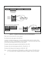
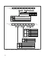
The H8 microcomputer by Hitachi is a single-chip microcomputer, but it is designed so that it can
also be used as a multi-chip microcomputer.
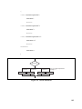
CPU
ROM
CPU
ROM
LCD
Periphery
RAM
RAM
Periphery
Periphery
Periphery
Single
System offers compact configuration
Multi
Little room for expansion
Each is configured of an individual IC
Can be easily expanded
(Signal conversion)
Figure 1.15 Multi and Single
1.3
Memory Data and Binary Values
Binary values are the basis of microcomputer operation. Let’s take a moment to review what
binary calculation is all about.
In digital processing, high and low voltages are used to express the numeric values of 0 and 1. All
information is expressed in terms of combinations of 0s and 1s. Because only two values are
involved, we call this “binary” processing.
In digital processing, only two states are used: high voltage and low voltage. There is nothing in
between. For this reason, even if the voltage level of the signal changes slightly, it is rarely
misjudged, meaning that this type of processing is not vulnerable to noise.
One binary digit is called a bit, and eight bits make up a byte. Other terms are also used, such as
“word”, “long word”, “quad word”, and “half word”, but there is no standard number of
configuration bits as defined by JIS. This is left completely to the microcomputer and the
manufacturer, so we will not go into it here.
16
The contents stored in the memory consist of combinations of 0s and 1s (binary values), but they
can mean completely different things. Instructions, data, and text are all expressed in binary
format.
1.3.1
Instructions and Binary Values
Although microcomputers may use the same operation instructions, they use different machine
languages (the instruction format expressed in binary format). The optimum language is used for
the microcomputer performance and application. For this reason, programs designed to run on a
personal computer will not run on a different microcomputer. In other words, programs are not
compatible. We will use the addition instructions for the H8 and Z80 microcomputers as an
example.
ADD instruction for the H8/300 series
Instruction stored in the memory (binary)
Instruction when the program is put together
(Machine language)
(Assembler)
1000000000000001
ADD.B #1, R0L
ADD instruction for the Z 80
1100011000000001
ADD A, 1
The H8 adds 1 to R0L, while the Z80 adds 1 to A. Both R0L and A are 8-bit memory locations
(called “registers”) in the microcomputer, and “1” is added directly to each as a result of these
instructions. The names are different, but both registers serve the same function. When expressed
in the binary format of the machine language, however, the instructions consist of different
combinations of 0s and 1s. So programs have to be created for the specific microcomputer
involved, and programs copied from one microcomputer to another will not run.
1.3.2
Numeric Expressions
The basic instructions of microcomputers are configured so that numeric values can be treated as
integers. Because the values are integers, there are no digits to the right of the decimal point.
There are two types of integer expressions: expressions that handle only positive values, and
expressions that handle both positive and negative values. Both are configured of combinations of
0s and 1s. There is no bit to express the sign. The 2’s complement is used to determine which type
of expression is used.
For example, if a numeric value using eight bits is expressed as 10000001, there would be a “1” in
7
0
the 2 bit and the 2 bit positions, so the values would be read as 128 + 1 = 129.
17
Binary
0
1
1
0
0
0
1
1
2 7 26 25 24 2 3 22 2 1 20
Bit weight
128 64 32 16
Decimal
8
4
2
1
64 + 32 + 2 + 1 = 99
Figure 1.16 Converting from Binary to Decimal Values
If this were expressed as data with a sign (2’s complement), however, it would appear as follows:
01111110
+
1
01111111
Each bit of original data is reversed
"1" is added
Result is data with reversed sign
1 0 0 0
0 0 0 0
MSB
negative,
( Ifif 0,1, positive
) This is not a + or - signal, however.
Figure 1.17 Signs and Reversed Signs
7
In comparison with the example showing a “1” in the 2 bit position, this value is 1 less, so the
result would be 128 – 1 = 127, and the answer would be –127. This method of calculation can be
used when converting from negative to positive, or from positive to negative. The MSB (Most
Significant Bit) of the negative data is 1, but this 1 does not represent a negative or minus signal.
This is just the way it happens to be. For 8-bit data, the combination of 0s and 1s would add up to
256. If there is no sign, an allocation of 0 to 255 would be used, but if there were a sign, the
allocation would be from –128 to 127.
8-bit, no sign
0
-128
255
127
8-bit, with sign
Figure 1.18 Bit Allocation for Binary Values (Numeric Line)
18
Depending on whether the program is viewed as data with or without a sign, the combinations of
0s and 1s express different data.
This may seem highly imprecise, but it works extremely well for the internal circuits configuring
the CPU. The same calculation method (circuit) can be used regardless of whether or not there is a
sign.
As an example, let’s look at the following addition.
(Decimal display)
(Binary value display)
(Without sign)
(With sign)
00000011
3
+3
+ 00001000
8
+8
00001011
11
+ 11
11110010
242
– 14
+ 11111010
250
–6
111101100
492
– 20
11110000
240
– 16
+ 00000001
1
+1
11110001
241
– 15
Do you see how it works? The correct result can be output by the same circuit, regardless of
whether or not there is a sign.
As seen here, the same combination of 0s and 1s produces a completely different result, depending
on whether or not the value has a sign. But there is only one instruction. An addition instruction
will produce an addition, whether or not there is a sign.
Table 1.1
4- to 32-Bit Numeric Values
No. of Bits
Without Sign
With Sign
4
0 to 15
-8 to +7
8
0 to 255
-128 to +127
16
0 to 65,535
-32,768 to +32,767
32
0 to 4,294,967,295
-2,147,483,648 to +2,147,483,647
19
Table 1.2
7-Bit Information Exchange Signs
b6
0
0
0
0
1
1
1
1
b5
0
0
1
1
0
0
1
1
b4
0
1
0
1
0
1
0
1
0
1
2
3
4
5
6
7
DC0 SP 0
@
P
`
p
A
Q
a
q
Parity bit
b7 b6 b5 b4 b3 b2 b1 b0
NUL
0
0
0
0
0
0
0
0
1
1 SOM X-ON
0
0
1
0
2
EOA
DC2
!
1
"
2
B
R
b
r
3
C
S
c
s
0
0
1
1
3 EOM X-OFF #
0
1
0
0
4
DC4
$
4
D
T
d
t
%
5
E
U
e
u
SYNC &
EOT
0
1
0
1
5 WRU ERR
0
1
1
0
6
RU
6
F
V
f
v
0
1
1
1
7
BEL
LEN
'
7
G W
g
w
1
0
0
0
8
BS
S0
(
8
H
X
h
x
1
0
0
1
9
HT
S1
)
9
I
Y
i
y
1
0
1
0
A
LF
S2
*
:
J
Z
j
z
1
0
1
1
B
VT
S3
+
;
K
[
k
{
1
1
0
0
C
FF
S4
,
<
L
\
l
|
1
1
0
1
D
CR
S5
-
=
M
]
m
}
1
1
1
0
E
SO
S6
.
>
N
~
1
1
1
1
F
SI
S7
/
?
O
↑
←
n
o DEL
Other decimal values
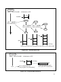
• BCD (Binary Coded Decimal)
This is a method in which values are expressed as binary values, but a decimal digit is expressed
every four bits, so if eight bits are used, decimal values from 00 to 99 can be expressed.
In applications where data is input by human beings, such as calculators, using BCD for the
microcomputer operation is convenient. Many microcomputers are configured so that BCD
operations can be carried out using a single instruction.
(Binary value)
(Decimal value seen as BCD)
00110100
34
10001001
89
20
1.3.3
Character Codes
Communication is often expressed in text format, particularly in applications such as Internet
communication. Different computers can communicate if they use the same characters. The text
information used here consists of character codes defined by ASCII (American Standard Code for
Information Interchange) or JIS or EUC (character codes used in UNIX). Seven-bit codes are the
same in all character codes, so we will look at this type of code here (refer to table 1.2).
When data created using a microcomputer is transferred to a personal computer, or when
instructions from a personal computer are being used to run a microcomputer, these codes are
used.
Chinese characters are expressed in 16 bits. JIS defines approximately 6,300 such character codes.
1.3.4
Decimal Point Data
Data operations involving data with decimal points are not often used in applications where a
microcomputer is incorporated into a device such as a household product, or in engine control.
Consequently, there is no instruction in the H8 that enables decimal point data to be calculated
with a single instruction. Because this is a standard data format, however, we will look at it here.
Floating decimal point data (a method of expressing data as a mantissa and an exponent, in which
the position of the decimal point is not fixed at a given bit position) is defined by IEEE 792, as
shown in the figure.
There are two types of data: 32-bit single precision and 64-bit double precision.
31 30 22
S exp
fraction
63 62
S
exp
Mantissa
0
Exponent
51
0
fraction
Sign
Figure 1.19 Floating Decimal Point
When data is processed by the H8, it is divided into the mantissa and the exponent, and is
calculated using an integer operation instruction.
21
(Bit no.)
(Address) 7
H'0000
H'0001
H'0002
0
8 bits = 1 byte
1 bit
H'FFFF
H'FFFF
Figure 1.20 Example of Memory Map
1.3.5
Expressing Numeric Values
We have talked about binary values and decimal values. If we only see the value “10”, however,
we don’t know which format is intended. If the value is binary and we convert it to decimal, it will
come out as 2, but if it is written as a decimal value, it will be 10. If we take an 8-bit value written
in binary format, it will be expressed as 10000000, which is long. So to distinguish between binary
and decimal, and to express binary values in a shorter form, many microcomputers use the
hexadecimal format. Binary values have (B’) at the beginning of the value, and hexadecimal
values have (H’). This method is used in the assembler in the H8 series.
1.3.6
Binary
B’10000000
Decimal
128
Hexadecimal
H’80
Memory Maps
A memory map indicates the memory space accessible by a particular microcomputer in map
format.
The microcomputer manages the memory by assigning addresses in units of eight bits. This is
common to most microcomputers, except for 4-bit microcomputers. Figure 1.20 shows a memory
map for a microcomputer that can handle 64-KB data.
If addresses are expressed in hexadecimal format, 64 KB of memory space can be expressed using
four digits (16 bits). In actuality, although we say 64 KB, it is actually 65,536 addresses. Because
10
the binary format is used for all of the expressions, this will be 1024 at the 2 position, which we
22
call 1 K. So 1 M = 1 K x 1 K, but because the original 1 K is 1,024 bits, 1 M will be 1,048,576
bits.
23
24
Chapter 2 H8 Microcomputers have High-Levels of
Performance and Functionality
2.1
What is an H8 Microcomputer?
‘H8 microcomputer’ is the generic term for Hitachi’s 8/16-bit microcomputers.
The H8 microcomputers are classified into two main series.
(1)
H8/500 series
H8/500 series models are mainly used for industrial applications and have more substantial errordetection functions than other models in the H8 series. It is easy to use an assembler to develop
programs, since many functions that can be executed as single instructions are available. A paged
mode is used when more than 64 Kbytes of data must be handled.
(2)
H8/300, H8/300H, H8S/2000 series
These microcomputers have a common instruction set.
• H8/300: standard 8-bit microcomputer
• H8/300L: low-power, low-cost 8-bit microcomputer
• H8/300H: standard 16-bit microcomputer
• H8/300H Tiny: compact 16-bit microcomputer
• H8S/2000: high-performance 16-bit microcomputer
H8S/2100: Application-oriented microcomputer. High-performance version of the H8/300
or H8/300L.
H8S/2200: High-performance version of the H8/300H, equipped with peripheral functions
suitable for consumer applications.
H8S/2300: High-performance version of the H8/300H, equipped with highly functional
timers and other features.
H8S/2600: Multiply-and-accumulate instructions are included. A multiplication is
executed in a minimal three clock cycles. This series provides the highest level of
performance series of all H8S-series products.
H8/300, H8/300H, H8S/2000 series microcomputers are low-priced and are widely used for the
control of televisions and VTRs and for inverter control, under the control panels and in the
internal LANs of automobiles, in cellular phones and ink-jet printers, etc.
H8/300-series devices handle 64-Kbyte memory spaces, while H8/300H, H8S/2000-series devices
handle 16-Mbyte memory spaces. Since the instruction set of these devices is comparatively
simpler, execution speeds are faster than for H8/500-series devices.
25
H8-series microcomputers
(development of CPUs)
H8S/2600
H8S/2300
H8/500
Multiply-and-accumulate circuit incorporated
Higher speeds
H8S/2200
Upward
compatibility
H8/300H
H8S/2100
Low power
16 bits
H8/300H Tiny
H8/300
8 bits
H8/300L
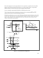
Figure 2.1 H8 Families
Since the CPU functions in terms of executing instructions are common within each series,
instructions can be shared. H8/500-series, and H8/300H, H8S/2000-series devices process up to
16 bits in each single instruction of most operations, while H8/300-series devices process 8 bits.
The H8/300H series is described below.
26
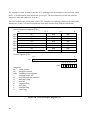
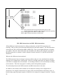
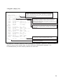
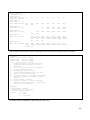
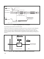
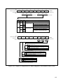
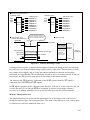
Development of the H8/3048 Series
Model Name
ROM/RAM capacity
Main peripheral functions
(an H8/300H-based product equipped with a 16-bit ITU)
Low-capacity memory
H8/3042 series
H8/3048 series
H8/3052F
64 kB/2 kB
DMAC 4 ch, TPC
ITU, ADC, DAC
128 kB/4 kB
DMAC 4 ch, TPC
ITU, ADC, DAC
256 kB/8 kB
DMAC 4 ch, TPC
ITU, ADC, DAC
100pin
H8/3035 series
256 kB/4 kB
ITU,TPC, ADC,
DAC
80 pins
compact
High-capacity memory,
high speeds, programming with
a single 5-V power supply
No on-chip ROM
H8/3039 series
H8/3003
128 kB/4 kB
ITU,TPC, ADC,
DAC
No ROM/512 bytes,
112 pins
DMAC 8 ch,
TPC, ITU, ADC
H8/3005
No ROM/4 Kbytes,
80 pins
ITU, ADC, SCI
Figure 2.2 Configuration of the H8/300H Series
The H8/300H series is a set of many products that have been developed around the same CPU on
the basis of types and storage capacities of on-chip memory, and of differences in on-chip
peripheral functions. The H8/3048F requires two power supplies, 12 and 5 V, for the
programming of its on-chip flash memory. The H8/3052F is equipped with the same peripheral
functions but only a single 5-V power supply is required to program its on-chip flash memory.
The H8/3052F is recommended to those who require a microcomputer for a new project.
2.2
Operation Mode of the H8/3048F
Features of the H8/3048F as a representative H8 microcomputer are summarized below.
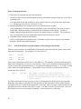
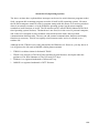
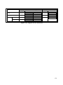
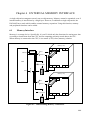
2.2.1
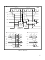
Summary
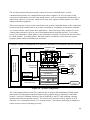
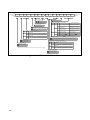
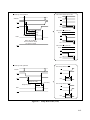
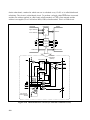
The H8/3048F is equipped with the H8/300H-series CPU. The H8/300H series was the first
product in which flash memory was used for on-chip ROM. The ‘ROM’ can thus be rewritten
even when the chip is being mounted on a board.
27
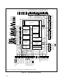
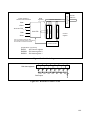
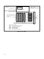
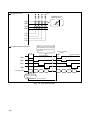
P40 /D0
P41 /D1
P42 /D2
P43 /D3
P44 /D4
P45 /D5
P46 /D6
P47 /D7
P30 /D8
P31 /D9
P32 /D10
P33 /D11
P34 /D12
P35 /D13
P36 /D14
P37 /D15
VSS
VSS
VSS
VSS
VSS
VSS
VCC
VCC
VCC
Port 3
Port 4
Address bus
Data bus (upper)
MD 1
Data bus (lower)
P53 /A 19
Port 5
MD 2
MD 0
P52 /A 18
P51 /A 17
P50 /A 16
EXTAL
P27 /A 15
Clock-pulse
generator
ø
STBY
RES
P26 /A 14
H8/300H CPU
P25 /A 13
Port 2
XTAL
VPP */RESO
Interrupt Controller
P66 /LWR
DMA controller
(DMAC)
P65 /HWR
P62 /BACK
ROM
(masked ROM,
PROM, or
flash memory)
P21 /A 9
P20 /A 8
P17 /A 7
P16 /A 6
P15 /A 5
P6 1 /BREQ
Port 1
P63 /AS
Port 6
P64 /RD
P23 /A 11
P22 /A 10
Bus controller
NMI
P24 /A 12
Refresh
controller
P60 /WAIT
P14 /A 4
P13 /A 3
P12 /A 2
RAM
P11 /A 1
P84 /CS 0
P81 /CS3 /IRQ 1
P10 /A 0
16-bit
integrated timer
unit (ITU)
P8 0 /RFSH/IRQ 0
2-channel serial
communication
interface
(SCI)
Programmable
timing pattern
controller
(TPC)
P95 /SCK 1 /IRQ 5
P94 /SCK 0 /IRQ 4
A/D converter
Port 9
P82 /CS2 /IRQ 2
Port 8
P83 /CS1 /IRQ 3
Watchdog timer
(WDT)
D/A converter
P93 /RxD1
P92 /RxD0
P91 /TxD 1
P90 /TxD 0
Note: * The VPP function is provided only for the flash memory version.
Figure 2.3 Internal Block Diagram
28
P70 /AN 0
P71 /AN 1
P72 /AN 2
P73 /AN 3
P74 /AN 4
P75 /AN 5
P76 /AN6 /DA 0
P77 /AN7 /DA 1
AVSS
AVCC
VREF
PA 0/TP0 /TEND 0 /TCLKA
PA 1/TP1 /TEND 1 /TCLKB
Port 7
PA 2 /TP 2 /TIOCA0 /TCLKC
PA 3 /TP 3 /TIOCB0 /TCLKD
PA 4/TP4/TIOCA1/A23/CS6
PA 5/TP5/TIOCB1/A22/CS5
PA 6/TP6/TIOCA2/A21/CS4
PA 7/TP7/TIOCB2/A20
PB 0 /TP8 /TIOCA 3
PB 1 /TP9 /TIOCB 3
Port A
PB 2 /TP10 /TIOCA 4
PB 3 /TP11 /TIOCB 4
PB4 /TP12 /TOCXA 4
PB5 /TP13 /TOCXB 4
PB6/TP14/DREQ0/CS7
PB 7 /TP15/DREQ 1/ADTRG
Port B
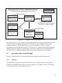
The on-chip peripheral functions mainly consist of inverter-controlled timers, a serial
communication interface for communication with a host computer, an A/D converter for the
conversion of information received from analog sensors, such as on temperature and humidity, to
digital form, and a D/A converter, which can be used as an output for audio signals or to control
analog-controlled equipment.
This microcomputer is in use as the control unit of an inverter-controlled motor, as the control unit
for the motor in the outdoor unit of an inverter-controlled air conditioner, as the motor controller
of a vacuum cleaner, and in many other applications. It has also been widely adopted for use in
cellular phones because of its low power consumption and on-chip flash memory. Even when
power is not supplied to a flash memory, the stored data is retained. New data can also be written
to a flash memory. In cellular phones, the flash memory can thus be used to store the system
program, phone numbers and addresses, and notes.
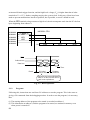
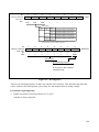
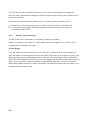
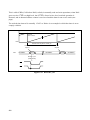
Example: System Configuration of an Inverter-Controlled Air Conditioner with the H8/3048
<Outdoor unit>
<Indoor unit>
IGBT module
Compressor
Base driver
Overcurrent
detection
Six-phase
PWM output
ITU
Driver
H8/3048
Outdoor
air temperature
Humidity
•••
Indoor control
microcomputer
M
Driver
H8/300HCPU
Stepper motor for
controlling
solenoid valves
M
M
Fan-motor control
Sensor
input
Communication with
the indoor unit
A/D converter
SCI
ROM
RAM
I/O port
Relay/switch
Direction-valve
control
Figure 2.4 System Configuration
The 16-bit integrated timer unit (ITU) generates the six pulse-width modulation (PWM) signals
(three positive-going signals and three negative-going signals) that are required to control the
inverter. A motor’s rotational frequency can be produced by the ITU, thus enabling constantspeed rotation and stop-position control. The current in the inverter circuit is input to an A/D
converter via a current trans former (CT) or shunt resistor. This allows monitoring of whether or
not the inverter circuit is operating correctly.
29
Inverter circuits are used in many electrical appliances such as air conditioners, refrigerators,
microwave ovens, and washing machines. When power that is generated by solar energy or the
force of the wind is used along with a business or domestic power supply, the inverter is used to
send power synchronously with the frequency of the power supply from the electric power
companies.
Flash memory acts as the on-chip ROM. Since a write circuit is included, all of the data in flash
memory can be rewritten by connecting a serial communication interface and a personal computer
while the chip remains mounted on its host board. Since rewriting can be executed in units of
blocks, part of an application or data can be modified while leaving the system program
untouched.
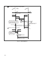
2.2.2
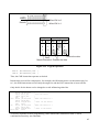
Single Chip
The H8/3048F can be used as a single-chip microcomputer. To designate single-chip operation,
the MD (mode) pins must be set. When the pins are set to seven (binary 111) and power is turned
on, single-chip operation is designated. To change the mode, turn off the power or reset the
microcomputer.
In this case, an address bus or a data bus will not connect the H8/3048F to such external modules
as memory or peripheral function modules. Only the 128 Kbytes of internal flash memory, 4
Kbytes of SRAM, and the on-chip peripheral functions are available for use. Since extended
address and data bus lines are not required, more pins are available for direct use in implementing
peripheral functions.
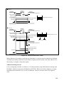
Figure 2.5 shows the memory map when single-chip operation has been designated. The address
range starting at H’00000 is assigned to the flash memory. On-chip peripheral functions are
allocated to the other part of the memory map.
30
Vector area
H'000FF
On-chip ROM
H'07FFF
16-bit absolute
addresses
H'00000
Memory-indirect
branch addresses
Mode 7
(single-chip advanced mode)
H'1FFFF
On-chip RAM
H'FFF00
H'FFF0F
H'FFF1C
H'FFFFF
Internal I/O
register
8-bit absolute addresses
H'FEF10
16-bit absolute addresses
H'F8000
Figure 2.5 Memory Map for a Single Chip
Allocation of peripheral functions as is done to the memory map on the H8/300H is called
memory-mapped I/O. Since this method allows I/O with the same instructions as are used for
memory operations, a variety of operations can be executed on I/O data. However, the space
available for memory is reduced since some of the memory is used for I/O.
In some microcomputers, on-chip peripheral functions are not allocated to the memory map and
there is a separate map for use with peripheral functions (the I/O map). This method has a merit in
that it allows more of the memory map to be allocated to memory. On the other hand, the method
has demerits in that I/O operations absolutely require use of the instructions that are exclusively
for the I/O map, and in that the functionality provided by instructions is at too low a level.
Which method is the best depends on the final product. Both methods have both good and bad
points. Memory-mapped I/O is adopted for the H8/300H, taking into consideration the affinity of
the C language to this approach.
31
2.2.3
Memory Expansion
When the setting on the modes is any number from one to six, the expanded mode is set for the
external expansion of memory. As a matter of course, peripheral functions can be connected in a
way that is much the same as the connection of memory. This mode is useful when on-chip
memory or on-chip peripheral functions are insufficient, or when a different type of memory is to
be used.
It is also possible to abandon the on-chip flash memory when the memory is expanded externally.
For instance, a maintenance program may be stored in the on-chip flash memory, with the system
program stored in the external memory space. Usually, the system program in the external
memory will be running. However, when, for example, a problem occurs after the product has
been shipped or when the product’s practical conditions of use are to be researched, the
maintenance program may be executed by simply changing the mode. If updating of the system
program is necessary, further flash memory can be connected as external memory.
The external memory space of 16 Mbytes is divided into eight 2-Mbyte units, called areas.
Memory of various types (including DRAM) and with different speeds can be managed by a
single chip in units of areas. For details, see section 6.
32
1-Mbyte mode
H'07FFF
External or
internal ROM
H'1FFFF
H'20000
H'3FFFF
H'40000
H'5FFFF
H'60000 External address
space
H'7FFFF
H'80000
H'9FFFF
H'A0000
H'BFFFF
H'C0000
H'DFFFF
H'E0000
H'0000FF
H'007FFF
16-bit absolute
addresses
Vector area
Memory-indirect
branch addresses
H'000FF
H'000000
16-bit absolute
addresses
Vector area
Memory-indirect
branch addresses
H'00000
16-Mbyte-mode
External or
H'01FFFF internal ROM
Area 0
Area 0
H'1FFFFF
H'200000
Area 1
Area 1
Area 2
H'3FFFFF
H'400000
Area 3
Area 2
Area 4
H'5FFFFF
H'600000
Area 5
External address
space
Area 6
Area 3
H'7FFFFF
H'800000
Area 7
Area 4
H'9FFFFF
H'A00000
External address
space
H'FFF1B
H'FFF1C
H'FFFFF
Internal I/O
register
Area 5
H'BFFFFF
H'C00000
Area 6
H'DFFFFF
H'E00000
Area 7
H'FF8000
On-chip RAM*
H'FFFF00
H'FFFF0F
H'FFFF10
External address
space
H'FFFF1B
H'FFFF1C
Internal I/O
register
H'FFFFFF
8-bit absolute addresses
H'FFEF0F
H'FFEF10
16-bit absolute addresses
On-chip RAM*
H'FFF00
H'FFF0F
H'FFF10
8-bit absolute addresses
H'FEF0F
H'FEF10
16-bit absolute addresses
H'F8000
Note: * External addresses, can be accessed by disabling on-chip RAM.
Figure 2.6 Externally Expanded Memory Map
33
2.3
Configuration of Registers and Programming
Both hardware and software are required to use microcomputers. Let’s study the software
(programs) first. With regard to hardware, a ready-made board is available for purchase and
immediate use.
2.3.1
Register Configuration
There are some temporary storage areas inside the CPU of a microcomputer. Copies of data
stored in memory or the results of operations and records of states on the way to these results are
temporarily placed in these areas. These temporary storage areas are called registers.
Almost all microcomputers can execute operations such as addition, subtraction, multiplication,
and division. They cannot, however operate directly on data in memory.
The reasons for this are:
(1) The instructions become long so that it takes much time to read them.
(2) Operations are seldom completed by one instruction so the possibility that the same data will
be used in the next operation is high. The execution time is thus shorter when the data is
closer to the CPU than memory.
The operation of an instruction becomes complicated when the microcomputer tries to directly
handle data stored in memory or to directly store the results of its processing in memory. For
example, consider the operation of an instruction of a microcomputer that adds data in memory to
each other and stores the results in memory.
The configuration of the instruction is as follows:
ADD source data 1, source data 2, result
(Instructions for execution by a microcomputer are written in a machine language, which consists
of combinations of bits with values 0 and 1. However, it is not easy for most human beings to
read machine language, so an assembler language is used to introduce the instructions. There is an
assembler-language version of every machine-language instruction.)
Instructions must be read before they are executed. How many bytes does this instruction have?
If the data and results are somewhere in memory and the memory space is 16 Mbytes then the
addresses must each have 24 bits. Therefore, three bytes of information are required to indicate
the each of the three addresses for data. Nine bytes are thus required because there are three
addresses. A further two bytes are required for the ADD instruction. So the instruction takes up
11 bytes.
The CPU does not know what to do until all 11 bytes of the instruction have been read. A
microcomputer with a data width of 16 bits can only understand the instruction after having
34
fetched data from the memory six times. What a long time that takes! There is a chance that the
result of this operation will be used in the next operation. It is outrageous if the next instruction
has to directly indicate the address of this result in memory.
MOV source data 1, register 1
MOV source data 2, register 2
ADD register 1, register 2, register 3
(The MOV instruction in this example is a transfer instruction but its actual operation here is to
copy the data. The original data in the memory is unchanged.)
In this case, a total of 12 bytes is necessary, five bytes for each MOV command and two bytes for
the ADD, so the number of bytes seems to have increased. When, however, operations continue
to use the data in memory, each ADD instruction only requires two bytes, so the number of bytes
taken up by instructions can be reduced. In addition, because the data used in the ADD instruction
is only a copy of the data in memory, that data remains in the memory. There is no problem if the
copy is lost, so it is OK to put the result of the ADD instruction in register 2, in the following way.
ADD register 1, register 2
35
Structure of an instruction (without registers)
ADD
Address 1
Address 2
Address 3
24 bits for
a memory space
of 16-M bytes
7
0
Address 1
Address 2
Address 3
Operation circuit
Memory
Structure of instructions (register-based)
MOV
Address 1
MOV
Address 2
ADD
7
0
Register
Address 1
Address 2
Register
Operation circuit
Memory
Figure 2.7 Structures of Instructions with and without Registers
That is why it is best for the CPU to have registers.
We will now look at the registers of the H8/300H.
A register is a temporary storage area, so it must be prepared with the right size (number of bits)
for the data it is to store. In H8/300H, three sizes are available, i.e., byte sized, word sized (16 bits
on this system), and long-word sized (32 bits on this system).
The names of the byte-sized registers are R0L, R0H, R1L, R1H⋅⋅⋅R7H.
The names of the word-sized registers are R0, R1⋅⋅⋅R7 and E0, E1⋅⋅⋅E7.
The names of the long-word-sized registers are ER0, ER1⋅⋅⋅ER7.
Note: Area R0 is actually made up of R0H and R0L, area ER0 is made up of E0 and R0, and so
on. If, for instance, R0L is changed, ER0 will also be changed. Take care on this point.
36
These registers are called general-purpose registers. ‘General-purpose’ here indicates that all of
the registers function in the same way and that any it’s possible to use any of these registers for
any of various purposes in the same way. The things that can be done in or with R0 are the same
things that can be done in or with R1 and R3. As one example of the things it’s possible to do ,
let’s start by looking at operations on data. In the case of
ADD.B
R0L, R0H
R0L and R0H are added and the result is placed in R0H. R0 is affected but E0 is not. In the case
of
ADD.W
R0,R1
R0 and R1 are added and the result is placed in R1. R1 is affected but E1 is not. In the case of
ADD.L
ER0,ER1
ER0 and ER1 are added and the results are returned to ER1.
Thus, general-purpose registers can be used to store the original data before an operation or the
results of an operation.
General-purpose registers are also used in another way, to indicate addresses of memory. For
example, the instruction to move a byte of data from memory to a general-purpose register is
MOV.B
@ <address of memory>, R0L
Three bytes of information are required to indicate an address of memory with a memory space of
16 Mbytes. Information that indicates the operation is naturally required as information in the
instruction, so the instruction takes up a total of six bytes. This instruction can also be used when
data is to be transferred from the indicated location a number of times.
MOV.B
@ER1, R0L
This 2-byte instruction uses general-purpose registers alone to indicate the address of memory.
The address is not input directly. Thus, there are cases in which it is best to use a general-purpose
register to indicate an address.
(@ indicates that an address of memory is given to the H8 microcomputer.)
Note: The parts on the right of the instruction are called operands. This means the targets of the
instruction. If there is more than one, they are separated by commas (,). The left-hand
part is called the source and the right-hand part is called the destination.
The CPU has other registers, too. These are control registers. They include the program counter
(PC) and condition-code register (CCR). The program counter indicates the addresses of the
instructions that are read out from memory.
37
If a program is stored in memory and the PC is pointing to the first address as shown in the figure,
the PC is incremented as each instruction is read out. The next instruction is read out, then the
instruction after that, and so on, in order.
The CCR indicates the current state of the CPU. Its behavior is strongly related to the individual
instructions, so the CCR will be introduced in the next section, along with the instructions.
General-purpose register (ERn)
15
0 7
0 7
0
ER0
E0
R0H
R0L
ER1
E1
R1H
R1L
ER2
E2
R2H
R2L
ER3
E3
R3H
R3L
ER4
E4
R4H
R4L
ER5
E5
R5H
R5L
ER6
E6
R6H
R6L
ER7
E7
R7H
R7L
(SP)
Control register (CR)
23
0
PC
7 6 5 4 3 2 1 0
CCR I UI H U N Z V C
<Legend>
SP
: stack pointer
PC
: program counter
CCR : condition-code register
I
: interrupt mask bit
UI
: user bit/interrupt mask bit
H
: half-carry flag
U
: user bit
N
: negative flag
Z
: zero flag
V
: overflow flag
C
: carry flag
Figure 2.8 General-Purpose Registers (a)
38
For use as 8-bit registers
7
0 7
R0H
R1H
R2H
R3H
R4H
R5H
R6H
R7H
0
R0L
R1L
R2L
R3L
R4L
R5L
R6L
R7L
For use as 16-bit registers
15
0 15
E0
E1
E2
E3
E4
E5
E6
E7
0
R0
R1
R2
R3
R4
R5
R6
R7
For use as 32-bit registers
31
0
ER0
ER1
ER2
ER3
ER4
ER5
ER6
ER7
Figure 2.8 General-Purpose Registers (b)
PC (Program Counter)
Instruction 1
Instruction 2
Instruction 3
Address containing an instruction
Counter is incremented after the instruction has been read out
Instruction 4
Memory
Figure 2.9 PC and Instructions
39
2.3.2
Instruction
H8/300H has many instructions. They are listed in the table below.
It might seem as if there are too many instructions. It is possible to write most programs with
approximately 10 instructions. This is because some instructions are rarely used and it is possible
to replace some instructions with other instructions.
So, only the basic instructions will be introduced here. Further instructions will be introduced as
required after this section.
The instructions for moving data from memory to a general-purpose register will be introduced
first. Many operations between the general-purpose registers of the H8/300H are available, so the
instructions for moving data to these registers are indispensable.
The MOV instruction is used to move data in this way. Data for MOV instructions can be
specified directly or by using general-purpose registers.
MOV.B
@H'10000,R0L
; The contents of the address H'10000 are
; copied to R0L.
MOV.W
R0,R1
; The contents of R0 are copied to R1.
MOV.L
ER0,@H'2000
; The contents of ER0 are copied to the
; address H'2000.
MOV.W
#B'10001000,R1 ; The contents of the address H'0088 are
; copied to R1.
(comments on the operations of a program are written after ";")
(one instruction can be written per line)
The data is stored in the destination written to on the right side of an operand. The MOV
instruction does not actually move data, but rather copies it.
40
Table 2.1
Instructions (all instructions in mnemonic form)
General data
movement
MOV
EEPMOV.B
Movement of data (copy) between memory and
general-purpose registers and between generalpurpose registers
EEPMOV.W
Block copy, .B is a 255- and .W is a 65535-byte
block
PUSH
Save
POP
Restore
ADD, ADDX
Addition, ADD X is with a carry.
ADDS
ADDS is for short-address calculation
SUB, SUBX
Subtraction, SUBX is with a carry
SUBS
SUBS is for short-address calculation
MULXU, MULXS
Multiplication, MULXU is unsigned, MULXS is
signed.
DIVXU, DIVXS
Division, DIVXU is unsigned, DIVXS is signed.
BCD operations
DAA, DAS
BCD-adjustment for arithmetic operations, DAA is
used after ADD and DAS is used after SUB.
Other operations
CMP
Data comparison
NEG
Inversion of the sign (plus/minus)
EXTU, EXTS
Extension of a bit, EXTU is unsigned, EXTS is
signed.
AND
Logical AND, bit by bit
OR
Logical OR, bit by bit
XOR
Exclusive OR, bit by bit
NOT
Inversion, bit by bit
SHAL, SHLL
1 bit shift to left (MSB side), SHAL is arithmetic
and SHLL is logical
SHAR, SHLR
1 bit shift to right (LSB side), SHAL is arithmetic
and SHLL is logical
ROTL, ROTXL
1 bit rotation to left (MSB side ), ROTXL is with a
carry bit.
ROTR, ROTXR
1 bit rotation to right (LSB side), ROTXL is with a
carry bit.
BSET
A single bit is changed to 1 (the byte is read out,
the bit is changed, and the byte is then written
back).
BCLR
A single bit is changed to 0.
BNOT
A single bit is inverted.
BTST
Checks whether or not a single bit is 0.
Control of a stack area
Arithmetic operations
Logical operations
Shift/rotation
Bit control
41
Carry bit control
Unconditional branch
Return
Conditional branch
42
BAND, BIAND
The logical AND of the carry bit and a specified
single bit is taken. The results are input to the carry
bit. BIAND specifies inversion of the single bit
operation.
BOR, BIOR
As above, but OR rather than AND.
BXOR, BIXOR
As above, but XOR rather than OR.
BLD, BILD
The specified single bit is written to the carry bit.
Otherwise as above.
BST, BIST
The carry bit is loaded as a single bit. Otherwise
as above.
BRA
Non-return branch (PC relative)
JMP
Non-return branch (absolute-indirect address)
BSR
Subroutine call (PC relative)
JSR
Subroutine call (absolute-indirect address)
TRAPA
OS call
RTS
Return from subroutine
RTE
Return from interrupt request processing or
TRAPA instruction processing
BNE
Branch when not equal.
BEQ
Branch when equal.
BHI
Branch when greater than, in terms of unsigned
data.
BCC (BHS)
Branch when greater than or equal, in terms of
unsigned data.
BLS
Branch when less than, in terms of unsigned data.
BCS (BLO)
Branch when less than or equal, in terms of
unsigned data.
BGT
Branch when greater than, in terms of signed data.
BGE
Branch when greater than or equal, in terms of
signed data.
BLT
Branch when less than, in terms of signed data.
BLE
Branch when less than or equal, in terms of signed
data.
BPL
Branch when positive or equal, in terms of signed
data.
BMI
Branch when negative or equal, in terms of signed
data.
BVS
Branch when an overflow is generated, in terms of
signed data.
BVC
Branch when no overflow is generated, in terms of
signed data.
Low power
consumption mode
SLEEP
Makes the transition to sleep or standby mode.
Control of CCR
LDC, STC
Loads/stores the one-byte CCR, as a single byte.
ANDC, ORC
Changes the CCR, in one-bit units.
XORC
Others
NOP
No operation
Endians
When data is moved between the memory and the register, it is handled as one byte over two
addresses if the memory data is one-word data, and as one byte over four addresses if it is longword data. Currently there are two types of microcomputers. In the H8/300H, smaller parts of an
address are in the upper side of the register (big endian).Some microcomputers such as Z80 use a
different order (little endian) than that of H8/300H.
Differences of endians observed in 16-bit data storage
n+1 address
n address
MSB
LSB
n address
n+1 address
Little endian
MSB
LSB
Big endian
Figure 1 Endians
Here we will describe operations. First, let’s look at addition.
ADD.B
R0L,R0H
;R0L + R0H -> R0H
ADD.W
#1000,R1
;1000 + R1 -> R1
ADD.L
ER0,ER1
;ER0 + ER1 -> ER1
(# is "immediate", which directly indicates a number. Numerations other than decimal
numeration can be used.)
A carry might be generated as a result of addition. A carry is stored in the C (carry) bit in the
CCR not in a general-purpose register.
R0H after the operation is H'00 (symbol (H') before the value indicates a hexadecimal numerical)
if the register values are set to R0L = H'80, R0H = H'80 before an instruction is executed.
43
In an operation of
ADD.B
R0L, R0H
;R0L + R0H -> R0H
Executed instruction
Data in the general-purpose register and CCR
ADD.B R0L,R0H
B'1000 0000 R0L
+) B'1000 0000 R0H
C= 1 B'0000 0000
With a carry
from the eighth bit
Z=1 The result of the eighth bit is 0
N=0
Positive in a signed data
V=1(Negative + Negative = Positive)
The data overflows from the eighth bit in signed data
Figure 2.10 Operation and CCR Changes
A carry is stored in the C bit in CCR; the carry never enters E0. In addition, the operation result is
0, so 1 is stored in the Z (0) bit in CCR. When this operation is carried out for signed data, the N
(negative) bit in CCR is 0 because 0 is a positive number. The answer is positive despite the
addition of a negative and a negative. However, this result cannot be recorded as 8-bit
information, therefore, 1 is stored in the V (overflow) bit in CCR. To decide whether a method for
operation must be changed as a result of a carry or overflow the content of CCR must be checked
after the addition. A method for changing processing flow will be introduced later.
Next, we’ll look at subtraction.
SUB.B
R0L,R0H
;R0H - R0L -> R0H
SUB.W
#10,R1
;R1 - 10 -> R1
SUB.L
ER0,ER1
;ER1 - ER0 -> ER1
When subtracting, be careful to note the directions for subtraction.
As with addition, the CCR is changed after having confirmed the results of the operation. In this
case, the C bit stores a borrowed value.
There is an instruction that does not return the results to the general-purpose register even
subtraction is carried out in the same way.
CMP.B
R0L,R0H
;R0H - R0L
This is an instruction to compare which is larger. Comparison is carried out for subtractions.
44
For another example, this instruction is used to compare the information of a sensor and a target
value to determine whether the target value has been attained. This instruction is different from
the SUB instruction, in that the results are not returned to the general-purpose register. CCR is
changed.
The current state can be recognized by CCR and a branch instruction can be used to change the
processing flow.
CMP.B R0L,R0H
BEQ TUGI
ADD.B #10,R0L
BRA SONOTUGI
NEXT:
SUB.B R0L,R0L
AFTERNEXT: MOV.B R0L,@H'2000
;
;
;
;
;
;
;
Compares R0L and R0H and then stores the contents of R0H to CCR
If equal, go to the line of NEXT and if not so, go to next ADD.
R0L + 10 -> R0L
Go to the line of AFTERNEXT unconditionally.
R0L becomes 0 with RL -R0L -> R0L
0 or data added by 10 is in R0L. It is transferred to the memory
of the H'2000 address
(Lines can be named. They are called as symbols, which are alphanumeric up to the 255th
character starting from the top and discriminating between lowercase and upper case characters.)
The BEQ (Branch EQual) instruction means "If equal, branch." On the contrary, " Branch if not
equal." is BNE (Branch Not Equal).
If the data is equal or can be confirmed by subtracting, the result is 0. This state is shown by Z = 1
in CCR. That is, the BEQ instruction means both equal and "The result is 0".
The meaning of each bit in CCRA is listed in Table 2.2.
The BRA (Branch Always) instruction is an instruction to branch unconditionally. This
instruction does not refer to CCR.
Table 2.2
Each Flag Bit of CCR
N: The result is "negative" if an operation is carried out by a signed binary.
Z: The result is "0".
V: The result is "overflow" if an operation is carried by a signed binary.
C: The result is "carry" or "borrow".
Next, We describe logical operations:
Some data make sense with one bit, rather than with eight bits, for example, they are information
on a sensor or an actuator. Consider an electric heating pot. If a button for boiling is set, the
microcomputer must turn on the heater when that button is pushed. The boiling button can take
only two states of being: pushed or not pushed. Either of these states can be expressed by one bit:
The state is expressed as 1 when pushed and 0 when not pushed. For a heater, the situation is the
same. One bit is sufficient because there are only two states: on and off. As before, when the
button is on the state is expressed as 1 and when it is off, 0.
45
A microcomputer checks the state of a switch or a heater’s on/off controls by exchanging data
with a memory.
A microcomputer has no special instruction to handle a sensor or to control an actuator. An MOV
instruction is used for reading from the switch. The MOV instruction also operates a heater.
However, the CMP instruction is not used to judge the switch’s state because MOV cannot read a
one-bit instruction even though it can be read as one byte data.
State of SW
H'4000
7
0
State of SW
Memory
R0L
The states of bits other
than SW are unknown
Figure 2.11 Input and Output Memory Map
This is an example showing data being read by the MOV instruction. The switch information is
supposed to be in the H'4000 address.
MOV.B
@H'4000,R0L
;(H' is an indication of hexadecimal.)
Certainly, the state of the switch is read in bit 0, but the states of other seven bits are unknown. In
this case, no CMP instruction can be used abruptly.
CMP.B
#B'00000001, R0L
;
It is acceptable if all seven bits other than the switch are 0, however, other states are not accepted.
Logical operational instructions are useful in this case. Unnecessary bits can be fixed to 0.
46
x
AND) 0
0
Result
0
x
0
0
0
x
0
0
0
x
0
0
0
x
0
0
0
x
0
0
0
x SW
01
00
01
When SW is 0
When SW is 1
Input
Output
A
0
B
0
AND
0
OR
0
XOR
0
0
1
0
1
1
1
0
0
1
1
1
1
1
1
0
Inverts the data
Data
Mask information Passes the data
Figure 2.12 Logical Operation
AND.B
#B'00000001,R0L
;
CMP.B
#B'00000001,R0L
;
Thus, the CMP instruction operates as desired.
Instructions are used for each purpose, for example, the OR instruction to set the unnecessary bit
to 1, the XOR instruction to invert only the target bit, and the NOT instruction to invert all bits.
Only the bit for the heater can be changed to avoid influencing other bits.
MOV.B
AND.B
CMP.B
BEQ
OFF: MOV.B
AND.B
MOV.B
BRA
ON:
MOV.B
OR.B
MOV.B
EXIT: BRA
@H'4000,R0L
#H'01,R0L
#H'01,R0L
ON
@H'4001,R0H
#H'FE,R0H
R0H,@H'4001
EXIT
@H'4001,R0H
#H'01,R0H
R0H,@H'4001
EXIT
;
;
;
;
;
;
;
;
;
;
;
Read the sensor
When the sensor is 0
*Turn off the heater
When the sensor is 1
*Turn on the heater
As will be explained in later programming, some instructions (instructions with *) can be
combined because they are redundant.
47
MOV.B
MOV.B
AND.B
CMP.B
BEQ
OFF:
AND.B
BRA
ON:
OR.B
WRITE: MOV.B
EXIT: BRA
@H'4000,R0L
@H'4001,R0H
#H'01,R0L
#H'01,R0L
ON
#H'FE,R0H
WRITE
#H'01,R0H
R0H,@H'4001
EXIT
;
;
; Read the sensor
;
;
;
;
;
; Control the heater
Two instructions were combined.
The number of instructions in a program can be reduced using subroutines to repeat the same steps
at different positions in a program.
To call a subroutine program, the instruction BSR or JSR is used. However, the RTS instruction
is used for returns.
BSR
JSR
SUB:
; Calling
; Calling
; Processing program in the subroutine
RTS
48
SUB
@SUB
; Return to the next instruction that has been called
Program
The difference in the two
instructions for calling subroutines
lies in whether @ is added or not.
The state of the stack area
and the stack pointer
after a subroutine has been called
SP(ER7)
SUB
JSR @SUB
Next instruction
PC
If two or more instructions are
for the same processing,
a program can be made smaller
by combining them into one.
BSR SUB
Next instruction
RTS
The state of the stack area
and the stack pointer
before a subroutine has been called
Not used
SP(ER7)
Used
Figure 2.13 Advantages of Subroutines
As shown, subroutines can be called repeatedly from anywhere. Naturally, the data to be returned
is the instruction following the instruction that has been called (instruction JSR or BSR). Why can
the program return? And to the next instruction that has been called at that!
A function called "stack" is used for this operation. In fact, during the execution of an instruction
that has been called (BSR or JSR), the program counter (PC) indicates the start address of the next
instruction. It is acceptable for this PC to be stored once elsewhere. The word "storage" reminds
us of registers or memory. Registers are acceptable, but their number is restricted and their
current use is unknown. Nothing is accomplished if the operation goes wrong even when the
program returns if the contents are destroyed. Therefore, most microcomputers use memory for
data storage. This particular memory area is called the "stack area".
In H8/300H, ER7, a general-purpose register, is used to indicate the address of a stack area that is
called a stack pointer (SP).
Let’s look at how it is used. The CPU writes the current PC to the memory area indicated by ER7
immediately when an instruction to call a subroutine is executed. Furthermore, when the RTS
instruction is executed, the instruction is read from the stack area to the PC. Thus, a mechanism is
established to return to the next address called from any location.
49
Then, what is the state of ER7? The answer is "undefined." That is, the address indicated is
unknown. In this situation, if the indicated memory device is a ROM, which cannot be written to,
the program cannot be returned. The mechanism to control whether the PC has been written to is
not incorporated into the CPU. The CPU does not know whether the system is in a state to return,
and it thinks that the data has already been stored. Therefore, the PC is read by an RTS instruction.
Then, the state of the PC address is unknown, so the program runs disorderly. We can identify the
RAM address to ER7 by a program.
MOV.L
#H'FFFF00,ER7 ; the H'FFFF00 address has been set
A subroutine sometimes calls a smaller subroutine. This is a nested structure subroutine. This
structure is unneeded when only one stack is used. So, ER7 stores PC after having been
decremented by 4 and it is returned to PC after having been incremented by 4 by the RTS
instruction. That is, the operation works like this: the stack area extends in the direction of the
smaller parts of the address as the nest deepens and releases the area used when it is returned.
A problem arises when the number of calls and returns do not coincide and the available RAM is
exceeded. When this happens, the CPU does not recognize that something is wrong. The system
runs disorderly. Programs must be written taking into account the estimated memory and an
estimate of stack size.
One use for a stack area is as a "saving area of the general-purpose register." A general-purpose
register has only one set of a main program or subroutine program. How a general-purpose
register is used in a main program is unknown, so a register used in a subroutine can be defined as
"Start to use after having been saved." However, a general-purpose register cannot be used as a
saving area for a genera-purpose register. If an unused address in RAM is known, it can be used.
However, it is not efficient if it is not released for another purpose after having been used. This
job is automatically carried out in the stack area. It is done in this way when the PC is saved. As
a stack area is always RAM, it is a desirable environment.
50
Program
MOV.L
#H'FFFF00,ER7 ; Initialization of SP
Not used
SP(ER7)
Used
SUB1
SUB2
JSR
@SUB1
Next instruction 1
SUB3
JSR
@SUB2
Next instruction 2
JSR
@SUB3
Next instruction 3
RTS
RTS
RTS
ER7
ER7
ER7
Instruction 1
address
Instruction 3
address
Instruction 2
address
Instruction 2
address
Instruction 1
address
Instruction 1
address
H'FFFF00
State of the stack area during the execution of each subroutine
Figure 2.14 Nest and Stack Area
Program
MOV.L
#H'FFFF00,ER7 ; Initialization of SP
SP(ER7)
Undefined
H'FFFF00
PC
RTS
PC is undefined and
"the program runs disorderly "
Restored from the stack
are by the RTS instruction
Figure 2.15 Program Runs Disorderly
51
SUB
MOV.L
MOV.L
JSR
@SUB
Next instruction 1
ER0,@-SP
ER1,@-SP
; Save
; Save
The general-purpose register
that has been saved
to the stack area can be freely used.
ER1
ER0
Instruction 1
address
MOV.L
MOV.L
@SP+,ER1
@SP+,ER0
; Restore
; Restore
Stack area
RTS
Note: Only word-size data or long-word-size data can be used
by general-purpose registers. Byte-size data cannot be specified.
MOV.L ER0, @-SP is the same as PUSH.L ER0.
MOV.L @SP+,ER0 is the same as POP.L ER0.
Figure 2.16 Save/Restore of a General-Purpose Register
Column
JSR / BRS instructions and JMP / BRA instructions
JSR and BSR are both instructions for calling a subroutine, and the RTS instruction is for
restoring. Why are there two instructions that function in the same manner? The JSR instruction
is described as JSR @SUB and the BSR as BSR SUB. There is the slight difference of whether
@ is added. However, when instructions are assembled, the address to be jumped is specified in
the JSR instruction, in contrast, a relative distance from the current PC is specified in the BSR
instruction.
What are the differences between them?
The JSR instruction does not change its memory address after it is once translated into machine
language to be changed into a load module. However, the BSR instruction can change its address
even after it is changed into a load module. It can change addresses to be stored freely according
to the situation. This form of program is called a position independent program.
The relationship between the JMP instruction and BRA instruction is the same.
In addition to this method, other methods can be adopted according to the configuration of
instructions, for example, instructions in a jump system can be branched to all memory space. A
branch using a general-purpose register or addresses to be jumped is arranged in memory. Branch
52
system instructions can use an 8-bit form as a relative address to be branched. It also has less
memory, and is faster than jump system instructions of 127 addresses ahead and 128 addresses
after. We recommend that a branch instruction be used for a nearby branch and that a jump
system be used for a distant branch or a jump table.
Operation is started by both instructions when stored in an address estimated at the time of linkage.
JSR
....
Call with an
absolute address
(H'1030)
SUB:
BSR
....
@SUB Call with a
relative address
(PC+H'30)
SUB:
....
....
SUB
Starting address which has
been estimated at the time of linage
(H'1000)
....
....
RTS
RTS
The JSR instruction does not normally operate when a load module is stored in a different address.
Starting address that has been
estimated at the time of linkage.
(H'1000)
Call with an
absolute address
has failed.
JSR
....
SUB:
....
....
RTS
BSR
....
@SUB Call with a
relative address
has succeeded.
SUB:
SUB
Staring address when an
actual memory is stored.
(H'2000)
....
....
RTS
Figure 3 Differences between JSR and BSR
2.3.3
Programming
Let’s try to write a program and execute it. Although it might seem to be difficult to write a
program, it’s easier than you expect.
As you can see when you look at the instruction set of the microcomputer, each instruction is only
able to do a small job. Using the microcomputer to do what you want depends on programming
the combination of instructions. The microcomputer doesn’t have an instruction to, for
example, maintain a comfortable temperature, because each instruction only does a small job.
53
Therefore, you have to break the task down to the level of instructions for the microcomputer.
The result of your breakdown may be as follows:
• Start by reading the room temperature through a sensor (MOV),
• compare the prescribed value with that room temperature (CMP),
• calculate some value to convert the difference between the temperatures into a target frequency
for the inverter (ADD, SUB, etc.),
• then, read the external climatic parameters through a sensor (MOV),
• calculate some value for adjusting the frequency of the inverter according to the external
climate (ADD, SUB, etc.),
• then, read the room’s humidity (MOV),
• calculate some value for adjusting the frequency of the inverter according to the humidity
(ADD, SUB, etc.),
• calculate the difference between the current temperature and the room temperature that was
initially read through the sensor (MOV, CMP),
• calculate how the air conditioner is working to adjust the frequency of the inverter (ADD,
SUB, etc.),
• determine the final frequency for the inverter,
• send the frequency of the inverter to the microcomputer of the external unit of the air
conditioner (MOV).
If you can break a task down as described above, you will be able to write good programs. It is so
easy, isn’t it?
Afterwards, we will shortly ask you to execute instructions and confirm the results of their
execution. You can, of course, learn about the instructions by simply reading this book, but it is
much more effective if you prepare the instruments, execute the program instructions, and confirm
the results on your microcomputer according to the instructions in this book. You will then have a
much better understanding of the functions of the microcomputer.
See the section ‘Preparations for the experiments’ included on the APPENDIX so that you can
prepare the required instruments. All of the programs for development are included on the
attached APPENDIX. Please copy these programs to the hard disk of your PC.
Firstly, input the program, even if you do not understand its meaning. In programming, imitation
is a great way to learn. Enter the program in text format. If you use word-processor software such
as WordPad, be sure to keep the program code in text format.
54
<List: add, subtract, multiply and divide operation>
.CPU
.SECTION
MOV.B
MOV.B
SUB.B
ADD.B
BCC
MOV.B
SET_ADD: MOV.W
MOV.B
SUB.B
MOV.B
MOV.B
MULXU.B
MOV.W
MOV.B
SUB.B
DIVXU.B
MOV.B
MOV.B
EXIT:
BRA
.END
300HA
PROGRAM,CODE,LOCATE=H'FFF000
@H'FF200,R1L
@H'FF201,R2L
R2H,R2H
R1L,R2L
SET_ADD
#1,R2H
R2,@H'FF202
@H'FF201,R2L
R1L,R2L
R2L,@H'FF204
@H'FF201,R2L
R1L,R2
R2,@H'FF206
@H'FF201,R2L
R2H,R2H
R1L,R2
R2H,@H'FF208
R2L,@H'FF209
EXIT
Name the file then save it. The required extension is ‘.SRC’.
Assembly
The program that you have entered is called a source program. This is the original program. The
source program is just a sequence of characters and is not machine language. An assembler is
used to convert the source program to the target machine’s language. Each line of the source
program is converted into an instruction of machine language by the assembler. The result is an
object file named *.OBJ. If the source program includes some grammatical mistakes, the
assembler displays ERROR. In this case, use the text editor to modify the source program then
assemble the source program again.
Linkage
This linkage may be slightly difficult to understand. Linkage is necessary to link files together
when software is developed in separate files by multiple programmers. The address of each
program is decided by this linkage process, so a program must be linked even when it is only
composed of a single program. In other words, the output of the assembler is relocatable object
code that has no addressing information (this file is called a load module and is named *.ABS.)
Errors will not occur. The message ‘Complete’ indicates that linkage is completed.
Execution by debugging monitor
Let’s execute and confirm your program on the H8/3048F. It is more pleasant than reading the
manual. Let’s take the challenge!
55
When the program is executed, the result appears in a moment. This is no problem if the result is
correct. If it is not, what should be done? It is then necessary to confirm the operation of each of
the program’s instructions in your head. That is, you must look at the source program line-by-line
and use your head as a simulator that works in the same way as the H8/300H CPU. You may
think ‘Why do I have to simulate those instructions in my head and act as the microcomputer?’ If
the program works well on the first run, there is, of course, no problem.
We now introduce a tool for use in program development. This tool has the following functions to
help you in debugging:
• Stopping the CPU after the execution of each instruction to confirm the contents of memory or
of general-purpose registers,
• Executing blocks of instructions until a selected instruction is executed, then stopping the CPU
after each execution of that instruction.
In other words, this tool for development makes it possible to confirm the state of the CPU during
the execution of the program, and is thus called a ‘debugging monitor.’
56
Source program
Creation of the source program
MOV
ADD
SUB
....
....
Text editor
Any text editor that is on the market
or is freeware is suitable
Filename.SRC
Object program
Assembly
01010101
11110000
10111001
....
....
Assembler
ASM38 filename
Provided by Hitachi, Ltd.
Filename.OBJ
Linkage
(concatenation)
Load module
Address information
Linkage editor
01010101
11110000
10111001
LNK filename
....
....
Filename.ABS
Transfer the object program
then execute it.
H8
Figure 2.17 Flow of Program Development (Up to the Debugging Stage)
Firstly, write the debugging monitor to the on-chip flash memory of the H8/3048F on the CPU
board that you bought or made. The procedure for writing is described in the chapter
‘Preparations for the experiments.’
The debugging monitor can store the program that has been developed by the user in RAM then
execute it. Before debugging, it is necessary to transfer files from the hard disc of the PC to the
CPU board. The file on the hard disc must be a load module file (*.ABS) rather than a source file.
The on-chip RAM with its size of 4 KB should be used first. The starting address for the program
is H’FFF000. You have seen that address, haven’t you? Yes, this address is used in the source
program in the following way:
57
.SECTION PROGRAM,CODE,LOCATE=H'FFF000
This line indicates that the subsequent line of program code should be placed at H’FFF000, the
starting address for the program.
It is possible to divide the program into several units, so-called sections. The name of this section
is ‘PROGRAM’, and its contents are ‘CODE’ (program). These names have the same format
restrictions as other symbols. Those lines that have a period (.) in their first column are not
instructions to be executed by the microcomputer. Such lines are used to control the assembler,
and are thus called ‘assembler directives.’
Open an MS-DOS prompt then execute the HTERM program that is provided on the APPENDIX.
Turn on the CPU board’s power supply. The startup message from the debugging monitor will
soon be displayed on the screen. Communications between your PC and the CPU board can now
be started. That is, it is now possible to operate the debugging monitor according to commands
from the PC. The symbol for the prompt that shows that the debugging monitor is waiting for a
command is the colon (:).
: L filename [Enter]
Check that the file has successfully been loaded.
: DA FFF000 [Enter]
How is this? This is slightly different from, yet similar to, the source program. Let’s execute the
instructions one by one, from the beginning of the program.
: .PC FFF000 [Enter]
: S [Enter]
How is this? It is possible to display the changes in the contents of general-purpose registers and
the PC after the execution of a single instruction.
What is done by the program will now be described below.
This program applies arithmetic operations such as addition, subtraction, multiplication and
division to data stored in the memory. There are two original data in memory at addresses
H’FFF200 and H’FFF201. The result of the addition is stored in H’FFF202, the subtraction in
H’FFF204, the multiplication in H’FFF206, the quotient in H’FFF209, and the remainder in
H’FFF208.
Use the M command to write some data to the addresses H’FFF200 and H’FFF201, by referring to
‘How to use the debugging monitor’ in the column of this book. Then, start the program from the
address H’FFF000 and execute the whole program to confirm its operation. The BRA instruction
is the last instruction of the program. The program will not continue after the BRA instruction
that is located at H’FFF03C has been executed. It is now possible to confirm the results of
execution at locations after H’FFF200, by using the all-display-function of the D command.
58
<Program> (smp2_2.src)
; Sample program
; Created on 2000.5.2
; Created by Y.Fujisawa
Use a semicolon (;) to insert comments in source program. For managing
the program, it is convenient to include such information as the purpose of
the program, the date and time of its creation, the version, etc. Japanese
characters can be used in the comments; only use one-byte characters
outside the comment portions.
.CPU
.section
mov.b
mov.b
SUB.B
ADD.B
BCC
MOV.B
SET_ADD:
MOV.W
MOV.B
SUB.B
MOV.B
MOV.B
MULXU.B
MOV.W
MOV.B
SUB.B
DIVXU.B
MOV.B
MOV.B
300HA
PROGRAM,CODE,LOCATE=H'FFF000
@H'FFF200,R1L ;DATA1 -> R1L
@H'FFF201,R2L ;DATA2 -> R2L
r2h,r2h
;0 -> R2L
R1L,R2L
;DATA1 + DATA2 -> R2L
SET_ADD
;if carry=1
#1,R2H
; 1 -> R2H
R2,@H'FF202
@H'FFF201,R2L
R1L,R2L
R2L,@H'FFF204
@H'FFF201,R2L
R1L,R2
R2,@H'FFF206
@H'FFF201,R2L
R2H,R2H
R1L,R2
R2H,@H'FFF208
R2L,@H'FFF209
;R2 -> ADD
;DATA2 -> R2L
;DATA2 - DATA1 -> R2L
;R2L -> SUB
;DATA2 -> R2L
;DATA1 * DATA2 -> R2
;R2 -> PRO
;DATA2 -> R2L
;0 -> R2H
;DATA2 / DATA1
;R2H -> REM
;R2L -> QUO
EXIT:
.end
BRA EXIT
;endless loop
The line starting with '.CPU' indicates the CPU name to be used.
One assembler can cope with all of the CPU's in the series from
H8/300 through to H8S/2000. This line is used to determine
whether the instructions used in the program are valid for the CPU
that is indicated on this line.
Although in labels such as PROGRAM or SET_ADD, uppercase letter
are distinguished from lowercase letters, they are not distinguished
from each other in program execution. Namely, they are treated in
the same way.
A line that has no characters (empty line) has no meaning.
Use empty lines to make your programs easier to read.
A line that starts with '.END' indicates the end of the file, and
must be placed at its last line.
The purposes of memory addresses must be indicated in comments. Otherwise, when the memory
address is used to store numeric data, it will be difficult to understand the program. It is
recommended that you name memory addresses in such cases.
59
<Program> (smp2_3.src)
.CPU 300HA
.SECTION PROGRAM,CODE,LOCATE=H'FFF000
DATA1 is the same as H'FFF200. @DATA1 is the same as @ H'FFF200.
MOV.B
MOV.B
SUB.B
ADD.B
BCC
MOV.B
@DATA1,R1L
@DATA2,R2L
R2H,R2H
R1L,R2L
SET_ADD
#1,R2H
MOV.W
MOV.B
SUB.B
MOV.B
MOV.B
MULXU.B
MOV.W
MOV.B
SUB.B
DIVXU.B
MOV.B
MOV.B
R2,@ADD
@DATA2,R2L
R1L,R2L
R2L,@SUB
@DATA2,R2L
R1L,R2
R2,@PRO
@DATA2,R2L
R2H,R2H
R1L,R2
R2H,@REM
R2L,@QUO
EXIT:
BRA
EXIT
DATA1:
DATA2:
ADD:
SUB:
PRO:
REM:
QUO:
.SECTION
.RES.B
.RES.B
.RES.W
.RES.B
.RES.W
.RES.B
.RES.B
WORK,DATA,LOCATE=H'FFF200
1
The program becomes easier to understand when the data are assigned
1
names. The symbol '.RES' is used to reserve the specified number of
1
the specified unit of memory. The numeric characters after the symbol
2
'.RES' show the number of units to be reserved. Here, for example,
1
one byte is reserved as DATA1. Although this is referred to as reservation,
1
it is still possible to access the region by address rather than by name.
1
SET_ADD:
;endless loop
.END
Naming regions of memory provides further convenience, when the address of a data area must be
moved. A program typically becomes larger and larger with each version of the program. As a
result, memory regions that have been in use become unusable. If the operands of the MOV
instructions of a program are written as by addresses, the address in all of the MOV instructions
must be modified. That is rather difficult to realize. In such a situation, if names have been given
to the memory regions in use, the required modification to the program for a given region is
localized to one line; the address given for LOCATE in the .SECTION line.
Let’s improve the program a little more. In this program, the data from DATA2 is loaded to
register R2L several times, because the content of R2L is changed by the execution of instructions.
As there are many general-purpose registers that are unused by this program, it is possible to copy
the content of R2L to a vacant general-purpose register and make the program execute more
quickly than the original program that reads data from memory several times.
As the data used in the original program are all very close together in the memory, loading the
addresses of those data into the vacant general-purpose registers and using indirect addressing is
an improvement, too.
60
<Program> (smp2_4.src)
EXIT:
.CPU 300HA
.SECTION PROGRAM,CODE,LOCATE=H'FFF000
MOV.L
#H'FFF200,ER0 ;set DATA1 address
SUB.L
ER1,ER1
MOV.L
#0,ER2
MOV.L
ER2,ER3
MOV.B
@ER0+,R1L
;Increment ER0 after reading the data
MOV.B
@ER0+,R2L
;Increment ER0 after reading the data
MOV.B
R2L,R3L
ADD.W
R1,R2
MOV.W
R2,@ER0
;ADD address
ADDS
#2,ER0
;SUB address
MOV.B
R3L,R2L
SUB.B
R1L,R2L
MOV.B
R2L,@ER0
ADDS
#2,ER0
MOV.B
R3L,R2L
MULXU.B
R1L,R2
MOV.W
R2,@ER0
ADDS
#2,ER0
DIVXU.B
R1L,R3
MOV.W
R3,@ER0
BRA
EXIT
.SECTION
DATA1: .RES.B
DATA2: .RES.B
ADD:
.RES.W
SUB: .RES.B
PRO:
.RES.W
REM:
.RES.B
QUO:
.RES.B
WORK,DATA,LOCATE=H'FFF200
1
1
1
2
1
1
1
.END
The performance of the program is improved and the amount of memory it requires has been
reduced.
(Refer to the APPENDIX manual ‘The execution time and bytes of instructions.’)
Column
How to Use the Debugging Monitor
The debugging monitor offers debugging functions via SCI 1. These include the following
functions:
• Loading a user program
• Executing the user program
• Break functions
• Modifying/displaying the contents of CPU registers
• Modifying/displaying the contents of memory and peripheral function registers
61
As a result, there are few restrictions on the debugging of programs, although there are some
restrictions on debugging SCI 1. After a program’s operation has been confirmed by using the
debugging monitor, the program can be loaded into ROM and executed as it is, as is the case for
the CPU for ‘model car rally’ is combined with the I/O board. In this case, there are no difficult
points such as modifications of addresses.
Monitor commands (use the help function for more details.)
• L
Load the program
• M
Alter/display the contents of memory and peripheral function registers
• D
Displays the contents of memory in a dump format
• R
Display the contents of CPU registers
• .
Alter the contents of CPU registers
• G
Execute the user program
• S
Execute the user program in single-step mode
• B
Set or display breakpoints
• H8 Display the contents of the on-chip peripheral function registers
• A
Simple assembly
• DA Disassembly
• ?
Help
Programming and Debugging
The CPU for ‘model car rally’ and the I/O board are used in the example below.
Prepare a program. The program EX1.SRC from the APPENDIX is used here as an example.
Open the program in your text editor to confirm the content of the file. This program makes each
of the eight LED’s correspond to the state of one of eight switches. These LED’s work as if they
are electrically connected to the switches, although they are not directly connected. The switches
and LED’s are only related to each other by the execution of the program.
Assemble and link the program.
>asm38 exl[Enter]
>lnk exl[Enter]
>HTERM[Enter]
Load the program before debugging into the SRAM that is externally connected to the CPU, rather
than to the on-chip flash ROM of the H8/3048F. Execute the program as a trial run. It is possible
to efficiently debug the program by the use of temporary stops and by alter/displaying the contents
of memory and peripheral function registers. Refer to ‘Preparations for the experiments’ for a
remainder of how to load the debugging monitor for the I/O board into the on-chip flash memory.
62
Start HTERM.
The prompt that shows that the debugging monitor is waiting for commands is the colon (:).
Confirm that this prompt returns after the Enter or Return key on the keyboard is depressed. The
channel for communications between your PC and the H8/3048F has now been established.
Load the program (from the PC to the H8/3048F).
:L EXl[Enter]
transmit address=001015
Top Address=000000
End Address=001015
:
The range occupied by the program will be displayed after it has been loaded. Confirm that these
addresses have the expected values. If they do not, check the source file or link the program
again.
Let’s execute the program.
:G 1000[Enter]
The hexadecimal number 1000 is the starting address of the program to be executed. Confirm the
starting address of the program before executing it. The communication channel between your PC
and the monitor program will be closed as soon as program being debugged is executed by the
monitor program. Inspect the board to confirm results during the program’s execution.
Change the positions of switches SW1 to SW8 to confirm the operation of this EX1 program.
Was the state of each switch successfully transferred to the LED? The bit position of each switch
is the same as that of the corresponding LED. An LED is lit when the corresponding switch has
been slid to its upper position and off when the switch has been slid to its lower position.
How does it work? It doesn’t work, does it?
Yes, this program has a bug. So, debug the program. Firstly, stop the execution of the user
program. As the communication channel to your PC has been closed during the execution of the
user program, the H8/3048F’s internal state is unknown. It is thus necessary to return to the
monitor program.
Press the NMI switch. The message that shows that a program has been aborted appears on the
screen and the monitor program’s prompt will reappear.
63
Abort at PC=00100A
PC=00100A CCR=80:I....... SP=00FFFF00
ER0=00000037 ER1=00000000 ER2=00000000
ER3=00000000 ER4=00000000 ER5=00000000
ER6=00000000 ER7=00FFFF00
:
When a program does not work properly, execute its instructions one by one (single-step
execution). Enter the S command, to execute the program from the address that the program
counter currently points to.
:S[Enter]
PC=00100C
ER0=00000037
ER4=00000000
00100A 28C7
:S[Enter]
PC=00100E
ER0=00000037
ER4=00000000
00100C 38D6
:S[Enter]
PC=00100A
ER0=00000037
ER4=00000000
00100E 40FA
:
CCR=80:I....... SP=00FFFF0000
ER1=00000000 ER2=00000000 ER3=00000000
ER5=00000000 ER6=00000000 ER7=00FFFF00
MOV.B
@H'FFFFC7:8,R0L
CCR=80:I....... SP=00FFFF00
ER1=00000000 ER2=00000000 ER3=00000000
ER5=00000000 ER6=00000000 ER7=00FFFF00
MOV.B
R0L,@H'FFFFD6:8
CCR=80:I....... SP=00FFFF00
ER1=00000000 ER2=00000000 ER3=00000000
ER5=00000000 ER6=00000000 ER7=00FFFF00
BRA
00100A:8
The contents of the general-purpose registers are displayed after the execution of each instruction,
and the execution of the program is stopped.
It seems that the data is being correctly input from the switches, because general-purpose register
R0L contains the data H’37. The writing operation also seems good, because the address
H’FFFD6 has been written to.
However, this data is not displayed.
If necessary, you can display or change the contents of memory (including of peripheral function
registers). Let’s change the content of the data register for port B that is connected to the LEDs.
:M FFFD6[Enter]
FFFFD6 0F ? 55[Enter]
FFFFD7 FF ? ^[Enter]
FFFFD6 0F ? 77[Enter]
FFFFD7 FF ? ^[Enter]
FFFFD6 0F ? 88[Enter]
FFFFD7 FF ? .[Enter]
:
How did that work? Has the display on the LEDs changed to reflect the expected value? It has
not changed. Moreover, the data before the change is always H’0F, so any data that has been
written was lost. It appears that the settings of the DDR, the register that decides the input/output
direction for the port’s pins, are wrong.
64
Now, use the M command again to change the value in the DDR. The address of the PBDDR is
H’FFFFD4.
:M FFFD4[Enter]
FFFFD4 FF ? FF[Enter]
FFFFD5 FF ? .[Enter]
:
Although the value at the address H’FFFFD4 appears to be H’FF, this value is not the value that
was actually set. This register cannot be read out, because it is a write-only register. Therefore,
write H’FF into the register, even though the displayed value in the register is already H’FF.
What’s the situation now? The states of the LEDs have been changed, haven’t they? PBDDR is
not initialized to the value H’FF by the program. The hardware of the LEDs seems to be normal
because the data is displayed well. Let’s confirm the hardware.
Take the following actions to confirm that there are no problems with the LEDs:
• Write H’FF and confirm that all of the LEDs are lit.
• Write H’00 and confirm that all of the LEDs are not lit.
Does this work well? How about the data H’AA or H’55? These two values are useful for
checking whether or not the bits are affected by their neighboring bits. It is a good idea to check
whether the bits are in a short-circuited state with their neighboring bits or not, as the pins of the
neighboring bits are close together.
:M FFFD4[Enter]
FFFFD6 88 ? FF[Enter]
FFFFD7 FF ? ^[Enter]
FFFFD6 FF ? OO[Enter]
FFFFD7 FF ? ^[Enter]
FFFFD6 OO ? 55[Enter]
FFFFD7 FF ? ^[Enter]
FFFFD6 55 ? AA[Enter]
FFFFD7 FF ? .[Enter]
:
How about the switches? Let’s read out their values.
After the M command is issued, the state of the switches at the moment when the Return key is
depressed is read once. If the switch settings have been changed, the address H’FFFFC7 should
be displayed anew.
The switch hardware is normal, if the displayed data changes as follows:
• The displayed data is changed to H’FF when all bits of SW are slid to their upper positions.
• The displayed data is changed to H’00 when all bits of SW are slid to their lower positions.
Confirm that there is no interference between neighboring bits, as with the LEDs.
65
:M FFFC7[Enter]
FFFFC7 37 ?[Enter] ->
FFFFC8 FF ?^[Enter]
FFFFC7 FF ?[Enter] ->
FFFFC8 FF ?^[Enter]
FFFFC7 OO ?[Enter] ->
FFFFC8 FF ?^[Enter]
FFFFC7 AA ?[Enter] ->
FFFFC8 FF ?^[Enter]
FFFFC7 55 ?.[Enter]
:
The state of the switches has changed.
The state of the switches has changed.
The state of the switches has changed.
The state of the switches has changed.
Is it true that PBDDR was not set correctly? Let’s look at the program in memory. Use the DA
command for disassembly.
:DA 1000[Enter]
<ADDR> <CODE>
001000 7A0700FFFF00
001006 5E001010
00100A 28C7
00100C 38D6
00100E 40FA
001010 F800
001012 38D4
001014 5470
001016 FF5D
001018 FFF6
00101A BADA
00101C AC75
00101E 8AF7
001020 6FF53ADF
001024 A767
001026 FCD7
:
<MNEMONIC>
MOV.L
JSR
MOV.B
MOV.B
BRA
MOV.B
MOV.B
RTS
MOV.B
MOV.B
SUBX
CMP.B
ADD.B
MOV.W
CMP.B
MOV.B
<OPERAND>
#H'00FFFF00:32,ER7
@H'001010:24
@H'FFFFC7:8,R0L
R0L,@H'FFFFD6:8
00100A:8
#H'00:8,R0L
R0L,@H'FFFFD4:8
#H'5D:8,R7L
#H'F6:8,R7L
#H'DA:8,R2L
#H'75:8,R4L
#H'F7:8,R2L
R5,@(H'003ADF:16,ER7)
#H'67:8,R7H
#H'D7:8,R4L
Memory areas with addresses above H’1010 do not contain parts of this program, so the original
data after the reset are displayed here. Neglect these values, whatever is displayed here.
The MOV instructions at H’1010 and H’1012 initialize the PBDDR. As the register R0L contains
the value H’00, PBDDR becomes set for the input of data. Modify the source program and try
again.
Make the change indicated below.
;---------- I/O initialize sub ------------IOINIT:
;
MOV.B
#H’00,R0L
;The bug is on this line; this data should
;be H’FF.
MOV.B
#H’FF,R0L
;
MOV.B
R0L,@PBDDR
;PB7-PB0 output
RTS
Assemble and link the modified program file. Use the L command to load the file thus created,
then use the G command to execute it from the address H’1000.
66
Does the program work well now?
The debugging monitor has some convenient functions other than those described above. In some
situations it is convenient to quickly execute a program to a prescribed address and then execute
further instructions one by one (single-step execution.) In this case, set a breakpoint at the address
from which execution will be in single steps. The command for disassembly is useful for
confirming the addresses of break points.
:DA 1000[Enter]
<ADDR> <CODE>
001000 7A0700FFFF00
001006 5E001010
00100A 28C7
00100C 38D6
00100E 40FA
001010 F800
001012 38D4
001014 5470
001016 FF5D
001018 FFF6
00101A BADA
00101C AC75
00101E 8AF7
001020 6FF53ADF
001024 A767
001026 FCD7
:
<MNEMONIC>
MOV.L
JSR
MOV.B
MOV.B
BRA
MOV.B
MOV.B
RTS
MOV.B
MOV.B
SUBX
CMP.B
ADD.B
MOV.W
CMP.B
MOV.B
<OPERAND>
#H'00FFFF00:32,ER7
@H'001010:24
@H'FFFFC7:8,R0L
R0L,@H'FFFFD6:8
00100A:8
#H'00:8,R0L
R0L,@H'FFFFD4:8
#H'5D:8,R7L
#H'F6:8,R7L
#H'DA:8,R2L
#H'75:8,R4L
#H'F7:8,R2L
R5,@(H'003ADF:16,ER7)
#H'67:8,R7H
#H'D7:8,R4L
The MOV instruction at H’100A transfers the data from SW to R0L.
Let’s set a break point at this instruction.
:B 100A[Enter]
:
Although the monitor gives no indication, the break point has been set correctly. Let’s confirm
this.
:B[Enter]
<ADDR>
00100A
:
These settings will make the program break at H’100A. Let’s execute the program.
67
:G 1000[Enter]
Break at PC=00100A
PC=001012 CCR=88:I...N... SP=00FFFF00
ER0=00000000 ER1=00000000 ER2=00000000
ER3=00000000 ER4=00000000 ER5=00000000
ER6=00000000 ER7=00FFFF00
:
Did the program stop correctly?
The break point is, of course, located before the instruction that will change the state of the LEDs.
The program counter points to the address of the instruction to be executed next.
Let’s start the single step execution from the address that is indicated by the above program
counter.
:S[Enter]
PC=00100C CCR=80:I....... SP=00FFFF00
ER0=00000055 ER1=00000000 ER2=00000000
ER3=00000000 ER4=00000000 ER5=00000000
ER6=00000000 ER7=00FFFF00
00100A 28C7
MOV.B
@H'FFFFC7:8,R0L
:
Has the LED display data been changed again?
The program can thus be debugged in the way described above.
[About the break point]
It is only possible to set break points at addresses in RAM. This is because the target instruction
at the break point is replaced with JMP instruction. This forces a call to the debugging monitor
during the execution of the user program that gives the impression that the execution of the user
program has been suspended. This is why a break point cannot be set at addresses in ROM, which
cannot be written to. The target instruction at the break point is replaced by the JMP instruction
when the G command is issued. Disassembly thus cannot be used to confirm whether or not the
replacement has taken place.
The contents of the on-chip peripheral function registers can be displayed in units of functional
modules by the H8 command. For example, the contents of the I/O ports are displayed in the
following way:
68
:H8 I/O[Enter]
<REG><ADDR> <CODE> < 7
P4DDR FFC5 FF
P4DR FFC7 01010101 D7
P4PCR FFDA 00000000
P6DDR FFC9 FF
P6DR FFCB .....111
P7DR FFCE 10001101 AN7
DA1
P8DDR FFCD FF
P8DR FFCF ...00000
6
5
4
3
2
1
0 >
D6
D5
D4
D3
D2
D1
D0
AN6
DA0
AN5
AN4
AN3
AN2
AN1
AN0
CS0
IRQ3
CS1
IRQ2
CS2
IRQ1
CS3
IRQ0
RFSH
RXD1
RXD0
TXD1
TXD0
P9DDR FFD0 FF
P9DR FFD2 ..111111
PADDR FFD1 FF
PADR FFD3 .0000011
PBDDR FFD4 FF
PBDR FFD6 00001010
TP15
DREQ1
ADTRG
SCK1
IRQ4
SCK0
IRQ5
TP6
TIOCA2
CS4
A21
TP5
TIOCB1
CS5
A22
TP4
TP3
TP2
TP1
TIOCA1 TIOCB0 TIOCA0 TEND1
CS6
TCLKD TCLKC TCLKB
A23
TP14
DREQ0
CS7
TP13
TP12
TP11
TP10
TP9
TP8
TOCXB4 TOCXA4 TIOCB4 TIOCA4 TIOCB3 TIOCA3
TP0
TEND0
TCLKA
:
The outline of and details on these commands can be obtained by using the help command:
:?[Enter]
Monitor Vector 01A258 - 01A357
Monitor ROM
01A358 - 01FD63
Monitor RAM
01FD64 - 01FFFF
User
Vector 000000 - 0000FF
.
:Changes contents of H8/300H registers.
A
:Assembles source sentences from the
:keyboard.
B
:Sets or displays or clear breakpoint(s).
D
:Displays memory contents.
DA :Disassembles memory contents.
F
:Fills specified memory range with data.
G
:Executes real-time emulation.
H8 :Displays contents of peripheral registers.
L
:Loads user program into memory from host
:system.
M
:Changes memory contents.
R
:Displays contents of H8/300H registers.
S
:Executes single emulation(s) and displays
:instruction and registers.
:
:M?[Enter]
Changes memory contents.
M <address> [;<size>] [RET]
<address> :memory address
<size>
:B -- byte
W -- word
L -- long word
:
HTERM can be terminated by depressing the ESC key.
69
Notes on using the monitor
• When the bus controller has not been initialized:
Set the best bus cycle by considering the memory performance and the frequency of the CPU’s
operating clock.
It is impossible for the H8/3048F to be fully utilized if the bus cycle is left in its initial state,
i.e., with the bus cycle set as 6 CPU-clock cycles.
• Interrupt handling by the monitor carries an overhead in terms of time:
The programming of interrupt handlers (including vector descriptions) is the same as on the
single chip. When an interrupt is generated, this is indicated on the display. For this to
happen, and before the interrupt is accepted, the monitor must be executed. This overhead is
why execution times become longer other than in solely ROM-access states.
• The NMI switch enables the user breaks:
After a user program is executed by the G command, control can be returned to the monitor
through a forced break (NMI interrupt).
2.3.4
Size of the Memory and Performance in Executing an Instruction
There are some variations in combinations of instructions that can be used to get the same result
from the microcomputer. For example, let’s clear ER0 to 0.
MOV.L
#0,ER0
XOR.L
ER0,ER0
SUB.L
ER0,ER0
Any of these instructions can be used to clear ER0 to 0. The numbers of bytes and the execution
times of the instructions are, however, not the same. The #0 part of the MOV instruction takes up
4 bytes, because this #0 means that the ‘0’ is expressed in longword format, i.e., as 32 bits. A long
time is taken to read this instruction. The numbers of bytes and the execution times of these
instructions are as follows:
MOV.L
#0,ER0 ;
;
;
;
The number of bytes in this instruction
(hereafter called the instruction length) is 6
bytes, and the execution time is thus at least 6
clock cycles.
The XOR instruction executes a logical exclusive-OR operation on the bits of the two operands.
When the same register is specified as both operands for this instruction, all bits of the operand
register become 0 as a result of the instruction’s execution. This is because a logical exclusive-OR
operation on two bits with the same value (1 and 1, or 0 and 0) creates a 0 in the result. However,
this instruction is not used extremely frequently, so the instruction is a little long.
70
XOR.L
ER0,ER0 ; The instruction length is 4 bytes, and the
; execution time is thus at least 4 clock cycles.
The best choice is the SUB (subtraction) instruction. When a SUB instruction is executed by
specifying the same register as both operands, all bits of that operand register will always become
0 as a result of the instruction’s execution. This is because subtracting something from itself
leaves 0. As this instruction is used very frequently, it has a short instruction code.
SUB.L
ER0,ER0 ; The instruction length is 2 bytes, and the
; execution time is thus at least 2 clock cycles.
While the MOV instruction is easiest to understand, the SUB instruction has the best performance.
Special care should be taken in selecting instructions, according to the purpose of the program, in
order to get a good performance.
Some other points to be considered are described below.
(1)
Executing multiply and divide instructions takes a long time.
Executing MULXn or DIVXn (n means S or U) instructions takes a long time, as shown below.
Instruction
Execution time
MULXU.B
14
MULXU.W
22
MULXS.B
16
MULXS.W
24
DIVXU.B
14
DIVXU.W
22
DIVXS.B
16
DIVXS.W
24
On the other hand, the execution time required to obtain the second power of an operand can be
reduced by using shift instructions. This is because the second power of the operand is then
obtained in only 2 clock cycles.
71
MOV.B
#2,R0L
; Executes @DATA/2 operation
MOV.W
@DATA,R1
; @DATA is data with no sign bit
DIVXU.B
R0L,R1
; The execution time of a DIVXU instruction is
: 14 clock cycles
MOV.W
@DATA,R1
; The same operation executed as shift
; instructions
SHLR.W R1
; The execution time of an SHLR instruction is 2
: clock cycles
Logical shift instructions can be used for multiply or divide operations on data that has no sign bit;
arithmetic shift instructions can be used on data with a sign bit. The meanings of the shift
instructions and examples of their usage are given below.
SHLL: Logical shift left
SHLR: Logical shift right
SHAL: Arithmetic shift left
SHAR: Arithmetic shift right
SHAR.L
ER0
;Divide 2
SHLL.W
E0
;Multiply 2
(2)
Development of subroutines
Subroutines are useful to reduce memory requirements. However, it is better not to use subroutines when the performance of a program takes priority over memory requirements, because it
takes a long time to call sub-routines.
It takes 2 or 4 clock cycles to execute a BSR or JSR instruction and 2 clock cycles for an RTS
instruction. In the worst case, 6 clock cycles are thus required to call a sub-routine. These clock
cycles are not necessary when the sub-routine is not used. A program calling a sub-routine 10
times requires 60 clock cycles; 100 times requires 600 clock cycles. Therefore, if the program
calls the sub-routine at most several times, the performance of the program in which no subroutine is used is better than that of a program in which sub-routines are used.
BSR
SUB:
SUB
...
RTS
; 2 to 4 clock cycles
; processing by the sub-routine
; 2 clock cycles
The merit of using a sub-routine is that the resulting program should be easier to understand. The
time required to debug the program can thus be shortened. Use fewer sub-routines when
execution times must be reduced.
(3)
Practical usage of 8-bits address
A memory space with a maximum address space of 256 bytes is called an 8-bit address space.
72
As few bits are required to specify an address within such a space, a reduction in memory
requirements can be expected. The instructions for operations on individual bits in memory can
only use the 8-bit address space. The bit number is specified as an immediate operand that is
expressed in the form #imm.
The 8-bit address space of the H8/3048F starts from H’FFFF00 and takes up 256 bytes. The space
is composed of on-chip RAM, with a size of 16 bytes, and peripheral functions. The RAM region
should be used with great care, because it consists of only 16 bytes. If this region is also used as a
stack region, the effectiveness of using the 8-bit address space is reduced by half.
MOV.B
@H'00:8,R0L
; 2 bytes, 4 clock cycles
MOV.B
@H'FF00:16,R0L
; 4 bytes, 6 clock cycles
MOV.B
@H'FFFF00:24,R0L
; 6 bytes, 8 clock cycles
H'FFFF00
On-chip RAM
H'FFFF0F
H'FFFF1C
On-chip peripheral functions
@ address : 8
(the memory region
that is accessed
by 8-bit addresses)
H'FFFFFF
16-MB memory space
Figure 2.18 Memory Map of the 8-Bit Address Space
73
(4)
Practical usage of the jump table
Processing by many programs variesaccording to the data to be processed. The processing by the
program becomes complicated if many CMP instructions are used to achieve this. Moreover, the
time required to process the data will vary according to the data. A jump table can be used to
solve such problems.
(In case of the use of CMP instruction)
MOV.B
@DATA,R0L
CMP.B
#H'00,R0L
BEQ SUB00
CMP.B
#H'01,R0L
BEQ SUB01
CMP.B
#H'02,R0L
BEQ SUB02
CMP.B
#H'03,R0L
BEQ SUB03
(In case of the use of the jump table)
MOV.L
#JMP_TBL,ER1 ; Acquires the starting address of the table
SUB.L
ER0,ER0
;
MOV.B
@DATA,R0L
;
SHLL.L ER0
; Converts the data to an offset address
; (multiplies by 4)
SHLL.L ER0
;
ADD.L
ER0,ER1
; Adds the offset address to the initial address
; of the table
JMP
@ER1
; Jumps
JMP_TBL:
.DATA.L
DATA:
SUB00,SUB01,SUB02,SUB03
; Registers the target addresses
; in the jump table
.RES.B 1
The performance or memory requirements of a program can thus be dramatically improved by
using the right mechanism in the program after the programmer has gotten a feel for the
characteristics of the CPU. The possibilities depend on the capabilities of the programmer. Of
course, the best programmer is the one who develops a program that works without error before
any of the others.
74
2.3.5
Basic Input and Output
It is not so interesting to operate on data in memory alone. This book covers the functions of the
microcomputer for you to study, so let’s try to control something. As a first step, let’s consider the
I/O ports. I/O ports are always included in single-chip microcomputers and can be used to great
advantage. Covering this function with respect to both hardware and programming is very simple,
so this function is suitable for beginners to learn.
DDR
memory
D
Q
Data written to
determine the
direction of the port
(input or output) Stored the direction
for the pin
(input or output)
Writing of
data for output
DR
memory
D
Q
I/O port pin
Stored data for
output from the port
Reading of
input data
Reading from
the address of DR
Figure 2.19 Structure of an I/O Port
Use the following as a rough guide in your thinking about I/O ports. There are some differences
with the approach to memory that has already been treated. Although the memory is used to hold
data, an I/O port is used to send data to or receive data from the pins. The microcomputer can be
made to write data to an I/O port by using an MOV instruction, just as with writing to a location in
memory. The data written to the pins then appears as voltages on the pins. This is called an
output port.
The microcomputer is also able to read data from an I/O port. This is just like reading from the
memory. The data that is read out from the port depends on the voltages which are being applied
to the port at the instant of reading; 1 is read out when the voltage is around 5 V, 0 when it is 0 V.
This is called an input port (refer to the column for more details on the digital voltage.)
75
I/O is an abbreviation for input/output. The use of I/O ports as both inputs and outputs is usual
because ports that are dedicated for use as either input or output provide less flexibility.
Although the description in the figure is of a single pin, the minimum data-bus width that is
available is 8 bits (1 byte), as with memory. Therefore the I/O ports are treated as groups of 8
pins. Let’s use this to turn on the LEDs by depressing the switches.
Construct the circuit shown in the figure.
Vcc
Vcc
Input port
Output port
(P40)
(PB0)
GND
State of SW and input data
SW Data
ON
OFF
0
1
Data output from and the state of each LED
Data LED
0
Lit
1
Not lit
Figure 2.20 Switches and LEDs
The pin attached to each switch is used as an input pin. The voltage level becomes high when the
switch is turned off and the information that is read out from the port is then 1; it becomes low
when the switch is turned on and 0 is then read out.
The resistance of a switch is very close to 0 Ω when it is in its ‘on’ state. The voltage at the switch
is 0 V according to Ohm’s law, because the pulling-up resistance and the 0 Ω resistance (switch in
its ‘on’ state) are connected in series if we assume that the resistance of the input port is ∞. When
the switch is in its ‘off’ state, the voltage at the switch is very close to 5 V according to Ohm’s
law, because the resistance of the switch is ∞.
The lamp is an LED (light-emitting diode). The port that is connected to the lamp is an output
port. The lamp is not lit by writing a 1 to the port; it is lit by a 0.
When an output pin is at 0 V, the difference between the voltage on the pin and the power supply
voltage is 5 V. This voltage difference is enough to make an electric current run through the LED.
An LED is a kind of lamp that is switched on when an electric current is passed through it. A
voltage of around 2 V is required to switch the LED on. In other words, the voltage and electric
current are not proportional in a LED, unlike in a resistor. The LED is, after all, a diode. Of the
voltage difference of 5 V, 2 V are applied to the LED, while 3 V are applied to the resistor. The
resistor is used to restrict the electric current that passes through the LED, because the LED may
be destroyed by excessive electric current (over 10 mA).
76
The difference between the voltage of an output pin and the power supply voltage becomes
effectively 0, when the former is close to 5 V. As this voltage difference is not enough to supply
an electric current through the LED, the LED is not illuminated. In other words, the electric
current can pass through the LED when the difference between the voltage on the output pin and
the power supply voltage exceeds 2 V, which is the threshold voltage of the LED. It is guaranteed
in the H8/3048F that the voltage on the output pin is set to [Vcc – 0.5] V, so the LED is certain to
be switched off.
Column
Electrical Characteristics and Absolute Maximum Ratings
There are three major electrical characteristics of any semiconductor; absolute maximum ratings,
DC characteristics, and AC characteristics.
Absolute maximum ratings: The semiconductor may result in permanent damage when it is used
in excess of the absolute maximum ratings (voltage, electric current, or heat). In that case, a
customer cannot ask the manufacturer to repair it under the guarantee.
DC characteristics: DC characteristics mainly consist of I/O voltages, power consumption, etc. In
designing circuitry, a customer can confirm whether or not it is possible to directly connect the
circuitry to the voltages on the I/O ports. The capacity of the power supply circuitry or
countermeasures for heat radiation can be considered by using these DC characteristics.
AC characteristics: AC characteristics indicate the behavior of signal ports in terms of the
propagation delay times, the differences in phase between clock pulses, set up times, hold times,
etc., while the I/O ports are being used within the range given by the DC characteristics.
77
Let’s enter and execute the program shown below.
<Program> (smp2_5.src)
P4DDR:
P4DR:
PBDDR:
PBDR:
LOOP:
.CPU
.EQU
.EQU
.EQU
.EQU
300HA
H'FFFFC5
H'FFFFC7
H'FFFFD4
H'FFFFD6
.SECTION
MOV.B
MOV.B
MOV.B
MOV.B
BRA
.END
P,CODE,LOCATE=H'FFF000
#H'FF,R0L
R0L,@PBDDR
@P4DR,R0L
R0L,@PBDR
LOOP
The LEDs turn on/off according to the on/off states of the switches. This program can rotate a
motor, when a motor rather than an LED is connected to the switch. This program can also be
used to make a heater heat up, when a heater rather than an LED is connected to the switch. It is
nice to know that a program can make something move, rather than simply manipulate the
contents of memory. Moreover, it is the programmer that has the program move that something.
Look at the source code of this program. Only the MOV instruction, which is the same instruction
that operates on memory, is used in this program. That’s OK. The switches or LEDs appear as
memory to the microcomputer. In other words, circuitry that allows a switch or LED to be treated
as memory has been added, because the microcomputer only has the functions to deal with
memory.
The circuitry that is used here is called an I/O port. The lamp is turned on by using the I/O port to
read the state of the switch. That is, an interface between the peripheral apparatus and the
microcomputer is established. This allows the microcomputer to receive information from the
outside or to give the result of an operation to something outside.
The I/O ports that are included in the H8/3048F can be configured as either inputs or outputs. The
DDR (Data Direction Register) decides whether the pins of an I/O port are used as inputs or
outputs. This register is different from the general-purpose registers, because it is assigned to a
memory location. This register is treated in the same way as memory by a MOV instruction. An
I/O pin is used as an output when the corresponding bit of the DDR is 1; as an input when it is 0.
The initial value of the DDR is 0; that is, the I/O pins are used as inputs. The DDR is set to 1
when the corresponding I/O pin must be used as an output. As the DDR cannot be read from, it is
impossible to confirm that a bit of the DDR has really been set to 1 after a 1 has been written to it.
The microcomputer and memory are analogous to the human brain. A human being has hands,
legs, mouth, nose, and ears. The microcomputer cannot become a system without having hands
and legs. The I/O port is the most fundamental shape of its hands and legs. The I/O port allows
78
the microcomputer to communicate with digital apparatus (the case which the microcomputer is
connected to the outside will be described in chapter 6.)
The program shown below can reverse the state of the corresponding LED every time the switch is
turned off. In other words, the LED is turned off by changing the state of the switch once, turned
on by changing it twice, turned off by changing it three times, turned on by changing it four times,
and so on.
<Program> (smp2_6.src)
P4DDR:
P4DR:
PBDDR:
PBDR:
LOOP1:
LOOP2:
.CPU
.EQU
.EQU
.EQU
.EQU
.SECTION
MOV.B
MOV.B
BTST
BEQ
BNOT
BTST
BNE
BRA
.END
300HA
H'FFFFC5
H'FFFFC7
H'FFFFD4
H'FFFFD6
P,CODE,LOCATE=H'FFF000
#H'FF,R0L
R0L,@PBDDR
#0,@P4DR
LOOP1
#0,@PBDR
#0,@P4DR
LOOP2
LOOP1
This BTST instruction can confirm the state of a single bit. The result of
the instruction is reflected in the Z bit in the CCR. Operation of the BEQ
and BNE instructions as branch instructions is based on the use of
the Z bit. The branch condition is satisfied when the Z bit is 0 in a BEQ
instruction. On the other hand, the branch condition is satisfied when
the Z bit is 1 in a BNE instruction.
The program, however, does not work as expected.
The cause of the malfunction is a phenomenon called jitter that arises from the structure of a
switch. This word ‘jitter’ refers to the state where the switch is repeatedly turned on and off over
a short period. The contact points of the switch do not touch in a sticky fashion like the suckers of
an octopus. When the switch goes to its on state, a pair of solid metal plates makes contact with
each other and bounce. Therefore, the initial signal levels repeatedly change between low and
high levels, and finally settle at the low level as is shown in the figure.
The jitter lasts for, at most, a few dozens of ms. This is a very short period from the viewpoint of
a human being. However, it is an extremely long time from the viewpoint of a microcomputer.
Over one period of 10 ms, when it is running at the clock of 16 MHz, the H8 is able to execute 80
thousands of those instructions which can be executed fastest, like the instruction for addition.
Therefore, a few dozens of ms is an extremely long time from the viewpoint of a microcomputer.
The actions from the confirmation of the input port by the BTST instruction to the turning over of
the bits by the BNOT instruction are repeated 4444 times in 10 ms. The jitter appears to quickly
turn the switch on and off many times. Whether the LED repeats its turning on and off
successfully or not depends on the number of state changes due to jitter and detected by the
program is even or odd. A special care should be taken in the debugging. It is possible to remove
the effect of the jitter by using an R-S type flip-flop.
79
Vcc
Vcc
Input port
Input port
GND
OFF
ON
ON
OFF
Signal at
the input port
Signal at
the switch
Occurrence of the jitter
Signal at
the input port
Figure 2.21 Jitter
However, costs increase because of this addition of hardware. This problem can be resolved by
programming. The answer is to simply check the state of the switch only after waiting for enough
time. In this case, you might think that the response will become slower because of this slow
checking of the state of the switch after it has changed state. This is no problem! The response
time of a human being is not as fast as the speed of the microcomputer or the jitter. For example,
can you press the button on a game controller 10 times a second? You do not press the button so
quickly, do you? The period taken to pressing the button is 100 ms, if you can achieve that.
Therefore, waiting 10 ms until the jitter ceases creates no problems.
80
<Program> (smp2_7.src)
P4DDR
P4DR
PBDDR
PBDR
LOOP1:
WAIT1:
LOOP2:
WAIT2:
.EQU
.EQU
.EQU
.EQU
.SECTION
MOV.B
MOV.B
BTST
BEQ
MOV.L
DEC.L
BNE
BNOT
BTST
BNE
MOV.L
DEC.L
BNE
BRA
.END
H'FFFFC5
H'FFFFC7
H'FFFFD4
H'FFFFD6
P,CODE
#H'FF,R0L
R0L,@PBDDR
#0,@P4DR
LOOP1
#10000,ER0
#1,ER0
WAIT1
#0,@PBDR
#0,@P4DR
LOOP2
#10000,ER0
#1,ER0
WAIT2
LOOP1
;Sets the time to wait
;Waits
;
;
;
;
;
;
;
;
This program is not efficient. We will consider the answer to jitter in the later section on the
timer.
Summary
The microcomputer only has the ports and instructions such as those that deal with memory. The
microcomputer can communicate with the I/O ports that are to it as the nerves of the hands and
legs are to a human being by using the same functions used to operate on memory. The hands and
legs of the microcomputer are the sensors that sense temperature, humidity, or acceleration, or
actuators such as motors or heater valves. The hands and legs of the personal computer are the
keyboard, mouse, camera, liquid-crystal display, etc. As such apparatus can be treated in the way
that has been described in the section on I/O ports, by connecting circuitry that appears, to the
microcomputer, to be equivalent to memory.
Column
Voltages and Digital Signals
The microcomputer treats digital signals as TTL or CMOS level. The output pin of an I/O port
operates at CMOS levels; input ports at TTL.
Therefore, logic circuitry that is constructed of TTL components can be directly connected to an
input port. This is also true of the output port.
In general, the input values of TTL levels are as follows:
Low level:
0.8 V or less,
High level:
2.0 V or more.
81
The input port of the H8/3048F operates on these voltage levels. The output voltage of the
circuitry that is connected should be as follows to match the two voltage levels:
Low level:
0.4 V or less (the noise margin is 0.4 V (= 0.8 V – 0.4 V),
High level:
2.7 V or more (the noise margin is 0.7 V (= 2.7 V – 2.0 V).
When the input voltage on the input port is 0.8 V or less, the read data becomes 0, while when the
voltage is 2.0 V or more, the read data becomes 1. When the input voltage on the input port is
between 0.8 V and 2.0 V, the read data is unpredictable. Therefore voltages in the range between
0.8 V and 2.0 V cannot be used as input voltages. The electric current at the input port is close to
0.
The input values for CMOS levels are as follows:
Low level:
1.35 V or less,
High level:
3.15 V or more.
The output voltage of CMOS circuitry is determined as follows so that the input voltage levels are
matched:
Low level:
0.1 V or less (the noise margin is 1.25 V (= 1.35 V – 0.1 V)),
High level:
Vcc – 0.1 V or more (the noise margin is 1.75 V
(= Vcc – 0.1 V – 3.15 V)).
The output pin of the H8/3048F has the following voltage levels.
Low level:
0.4 V or less (when 0 has been written into the data register),
High level:
Vcc – 0.5 V or more (when 1 has been written into the data register).
The amount of electric current from an output pin depends on the pin. For the general purpose
pins, it is between 2 and – 2 mA. The output voltage changes when the electric current is taken
out. The output voltage levels described above are guaranteed when the output electric current is
in the range from 1.6 mA to – 200 µA.
Ports 1, 2, 5, and B are for large electric currents. Pins on these ports can each pass 10 mA as a
maximum electric current, when they output the low-level voltage. It is convenient to use those
ports to turn on the LED, because driver circuitry can then be omitted.
82
Column
Input Circuitry and Driver Circuitry
The levels of input and output voltages of the I/O ports are TTL/CMOS. When an input port is
used to check the state (on/off) of a switch, circuitry must be designed so as to change the input
voltage according to that state (on/off). The voltages of 0 V in the on state and 1 V in the off state,
can be applied to the input port, when a resistor is connected in series with the switch.
Now, let’s look at the value of this resistor. If the resistance is too small, a large electric current
will pass when the switch is turned on. When the resistance is 100 Ω, for example, the electric
current save 0 mA with the switch in its off state and 50 mA with the switch in its on state. This
current of 50 mA is the same as the total consumption of electric current by the H8/3048F. That
is, to check whether a switch is in its on state or not, the same amount of electric current must be
consumed as is consumed by the microcomputer.
Vcc
ION = Vcc/R
R
Input port
GND
Almost all of the electric current passes through the switch.
When R = 100 , ION becomes 50 mA.
This current is large because 50 mA is the same value as
the amount of electric current consumed by the H8/3048F.
It is better to use a pull-up resistor with a large resistance
such as several k , for example, to realize a low power consumption.
R
Input port
VOFF=5 X
GND
Input capacitance
Floating
capacitance etc.
in the wiring lead
t
(1 - e- CR )
When the switch is turned off, these capacitances are charged with electric current
through the pull-up resistor. If the resistance of the pull-up resistor is too large,
the transition to the high level takes a long time.
Input
signal
On
Off
Figure 4 Pull-up Resistor
However, further problem is introduced when the value of the resistor is too large. The input port
is connected to the transistor inside the circuitry, and has an input capacitance, which is a
component of capacitor and comes from the structure of the transistor. There is a floating
capacitance, which is the component of capacitor, of the wiring leads. It is necessary to charge
these capacitors to make the resistor high level. As it takes a long time to charge these capacitors
when the value of the resistor is too large, the high level is only reached at the input port a long
time after the switch is turned off. Therefore, it is not good to have too large value for the resistor.
83
Load
Ports 1, 2, 5, and B
Vcc
Up to 10 mA
Output port
Load
Load
CMOS-IC
Up to 50 mA
Vcc
Load
Open-collector IC
Up to dozens of A
Darlington-connection
type NPN transistor
Output port
Up to 36 mA
Output port
Load
Load
Up to several-hundred mA
Output port
NPN Tr
Output port
PNP Tr
Up to dozens of A
Output port
N-ch FET
Output port
P-ch FET
Load
Load
When the load needs
to be driven with low level
Figure 5 Examples of Driver Circuitry
Vcc
Photo-coupler
(insulation by means of light)
Output port
Pulse transformer
(insulation by means of magnetic fields)
Figure 6 De-coupling (Photo-coupler and Pulse Transformer)
The normal value is in the range of several kΩ to several hundreds of kΩ.
84
An LED can be directly driven by an output pin, while a motor cannot, because a large electric
current cannot be drawn out of an output pin. It is necessary to connect driver circuitry to amplify
the signal level. Ports for large electric currents or circuitry that can apply 50 mA with standard
logic levels can be used for loads such as those that require small electric currents and can be
driven by 5 V. The open-collector, open-drain, or an interface of the standard logic can be used
for those loads that can be driven by 5 V or more. A transistor must be used to handle a larger
electric current or voltage. A given apparatus can thus be driven by using driver circuitry that is
externally connected to the output pin to amplify the signal level, when the electric capacity of the
output pin is not enough to drive it.
An apparatus that requires a high AC voltage, such as 100 V, must be driven after electrically
isolating the transistors that drives the apparatus from the output port. Such a structure can
prevent damage to the microcomputer even when the transistors have been destroyed. Light or
magnetic fields are used to achieve the electrical isolation. A photo-coupler is used for electrical
isolation by means of light, and requires that the output pin supplies it with DC current. A pulse
transformer or the like achieves electrical isolation by means of magnetic fields.
The signal from the output pin must be pulse-shaped in this case, because magnetic power cannot
be transferred to the other side of the pulse transformer unless the magnetic power is in a state of
change.
Column
I/O Ports of the H8/3048F
The I/O ports can be used for the input or output of data. They are necessary for the
microcomputer to control the system, for example, for the input of data from a sensor, or the
control of actuators.
It is possible to change the direction of signals (input or output) on the I/O ports. Signals can be
read from outside the microcomputer when an I/O pin is set as an input. The level of a pin to
which high level (2.0 V or more) has been applied becomes 1 when the CPU reads it out by a
MOV instruction etc., while the level of a pin to which low level (0.8 V or less) has been applied
becomes 0. I/O ports can thus handle input voltages at what is called TTL levels.
Data which has been written by the CPU with a MOV instruction etc. can be output at a port when
the I/O port is set as an output. The written data can be held until the next round of writing. In
other words, the I/O port can also retain data as if it were a memory. The ‘high’ voltage level
(Vcc – 0.5 V or more) is output on a pin to which 1 has been written, while a ‘low’ level (0.4 V or
less) is output when a 0 has been written. These levels are the CMOS levels.
The addresses that are accessed by this CPU are all in a single address space that includes the
memory (the H8/3048F does not have the other I/O space than memory space, while the 80-series
CPU have.) The addresses that are accessed by the CPU as I/O exist in a prescribed and fixed
85
range (namely, H’FFFF1C to H’FFFFFF in the memory map; the portion that is assigned to onchip I/O).
There are a total of 78 ports available on the H8/3048F. However, that figure includes ports that
will in practice be used for other purposes such as for the address and data bus of the memory
interface, and for control signals. As a result, the number of available I/O ports will be reduced
when memory is connected from the outside.
Table 1
Address
H'FFFFC0
H'FFFFC1
H'FFFFC2
H'FFFFC3
H'FFFFC4
H'FFFFC5
H'FFFFC6
H'FFFFC7
H'FFFFC8
H'FFFFC9
H'FFFFCA
H'FFFFCB
H'FFFFCC
H'FFFFCD
H'FFFFCE
H'FFFFCF
H'FFFFD0
H'FFFFD1
H'FFFFD2
H'FFFFD3
H'FFFFD4
H'FFFFD5
H'FFFFD6
H'FFFFD7
H'FFFFD8
H'FFFFD9
H'FFFFDA
H'FFFFDB
Addresses of the I/O Port Registers
Register
Name
P1DDR
P2DDR
P1DR
P2DR
P3DDR
P4DDR
P3DR
P4DR
P5DDR
P6DDR
P5D
P6DR
—
P8DDR
P7DR
P8DR
P9DDR
PADDR
P9DR
PADR
PBDDR
—
PBDR
—
P2PCR
—
P4PCR
P5PCR
Bit 7
P17DDR
P27DDR
P17
P27
P37DDR
P47DDR
P37
P47
—
—
—
—
—
—
P77
—
—
PA7DDR
—
PA7
PB7DDR
—
PB7
—
P27PCR
—
P47PCR
—
Bit 6
P16DDR
P26DDR
P16
P26
P36DDR
P46DDR
P36
P46
—
P66DDR
—
P66
—
—
P76
—
—
PA6DDR
—
PA6
PB6DDR
—
PB6
—
P26PCR
—
P46PCR
—
Bit 5
P15DDR
P25DDR
P15
P25
P35DDR
P45DDR
P35
P45
—
P65DDR
—
P65
—
—
P75
—
P95DDR
PA5DDR
P95
PA5
PB5DDR
—
PB5
—
P25PCR
—
P45PCR
—
Bit Name
Bit 4
P14DDR
P24DDR
P14
P24
P34DDR
P44DDR
P34
P44
—
P64DDR
—
P64
—
P84DDR
P74
P84
P94DDR
PA4DDR
P94
PA4
PB4DDR
—
PB4
—
P24PCR
—
P44PCR
—
Bit 3
P13DDR
P23DDR
P13
P23
P33DDR
P43DDR
P33
P43
P53DDR
P63DDR
P53
P63
—
P83DDR
P73
P83
P93DDR
PA3DDR
P93
PA3
PB3DDR
—
PB3
—
P23PCR
—
P43PCR
P53PCR
Bit 2
P12DDR
P22DDR
P12
P22
P32DDR
P42DDR
P32
P42
P52DDR
P62DDR
P52
P62
—
P82DDR
P72
P82
P92DDR
PA2DDR
P92
PA2
PB2DDR
—
PB2
—
P22PCR
—
P42PCR
P52PCR
Bit 1
P11DDR
P21DDR
P11
P21
P31DDR
P41DDR
P31
P41
P51DDR
P61DDR
P51
P61
—
P81DDR
P71
P81
P91DDR
PA1DDR
P91
PA1
PB1DDR
—
PB1
—
P21PCR
—
P41PCR
P51PCR
Bit 0
P10DDR
P20DDR
P10
P20
P30DDR
P40DDR
P30
P40
P50DDR
P60DDR
P50
P60
—
P80DDR
P70
P80
P90DDR
PA0DDR
P90
PA0
PB0DDR
—
PB0
—
P20PCR
—
P40PCR
P50PCR
Module
Name
Port 1
Port 2
Port 1
Port 2
Port 3
Port 4
Port 3
Port 4
Port 5
Port6
Port5
Port6
Port 8
Port 7
Port 8
Port 9
Port A
Port 9
Port A
PortB
Port B
Port 2
Port 4
Port 5
Note: A bit position that is indicated as — has neither port nor memory function.
Moreover, as the ports serve both as I/O ports and as ports for the on-chip peripheral functions, the
number of available I/O ports will be further reduced.
An I/O port has the simple structure shown in figure 2.19, with the port controlled by two
registers; DDR (Data Direction Register) and DR (Data Register).
• DDR (Data Direction Register)
This register determines the direction of the port pins (input or output).
0: The pin is used as an input (initial value)
86
1: The pin is used as an output
• DR (Data Register)
This register handles data for the port. The meaning of this register depends on the settings of
pin directions (input or output). When a pin is set as an input (DDR = 0), the input value at
TTL level can be determined by reading the DR as follows:
0: A low-level voltage has been input to the port
1: A high-level voltage has been input to the port
When it is set as an output (DDR = 1), a value at CMOS level can be output after writing to the
DR as follows:
0: A low-level voltage is output from the port
1: A high-level voltage is output from the port
Note: These two registers represent a kind of memory function that is used to control the I/O
ports and differ from the general-purpose registers of the CPU, although they are still
called registers. They are mapped to the memory map of the H8/3048F. In other words,
these registers are accessed by specifying their addresses. They are treated in the same
way as memory.
The I/O ports are normally treated as groups of 8 pins, because the minimum unit of the memory
in the CPU is the byte (= 8 bits). Individual I/O pin can, however, be treated as independent ports.
Table 1 shows the register configuration of the ports of the H8/3048F. Over 70 I/O pins are
available. The pull-up MOS control registers (PnCR) will be explained later.
Program
Any instruction that is used to access locations in memory, such as MOV, BSET, can be used to
deal with the pairs of I/O registers.
Initialization
The direction for the pins on each I/O port (input or output) is set in the DDR.
After a reset operation, the DDR is initialized so that all pins are set as inputs. It is thus only
necessary to alter the DDR setting when an I/O port is needed as an output port. The following
program sets all 8-bit ports as outputs.
MOV.B
#H'FF,R0L
MOV.B
R0L,@DDR
(The address of the DDR must be declared with the EQU directive instruction before any
reference to @DDR.)
The following program can be used to set the bits in position 0 as an output and the remaining 7
bits as inputs.
87
MOV.B
#H'01,R0L
MOV.B
R0L,@DDR
Instructions for bit-wise operations cannot be used on the DDR, because the DDR is write-only.
Therefore, the following usage is wrong.
BSET
#1,@DDR
Although a source program that includes this line will be assembled without error, all of the
specified I/O ports can be changed to the output. The instruction for bit-wise operations reads 1
byte of data that includes the 1 bit that is the operand of the instruction, changes only that bit, then
finally writes back 1 byte of data that includes the 1 bit. The instruction for bit-wise operation
thus reads, modifies, and writes in a single process. The DDR is, however, write-only so the value
set in it cannot be read. The data, which is read from the DDR that cannot be read out its value by
an instruction for bit-wise operation, is thus unpredictable. Normally, as the data bus will have
been pre-charged (‘pre-charged’ means that the data bus has been charged to half of the powersupply voltage, and the time required to make the transition from the pre-charged to the high or
low state is less than that required for high to low or low to high), all bits will be read out as 1.
The bit position 0 of the read out data (H’FF) is then modified to 1, and the modified data (H’FF)
is then returned to the DDR. As a result, all of the specified I/O pins including those that were
intended to be inputs, are turned into outputs.
So all of the bits have been turned into outputs, although the intention was to only switch one bit
from input to output. The program thus will not work as you might have expected. Take care on
this point.
Now, let’s use a program to connect the LED and switch shown in figure 9. This program turns
on an LED when the corresponding switch has been turned on. That is, although they are not
electrically connected, the program makes them operate as if they were electrically connected.
Vcc
4.7kΩ
P70
GND
74LVC08
PA0
330Ω
Figure 9 Example of Input and Output Circuits for the I/O Port
88
The program for inputting and outputting the data
The switch is connected to port 7. Port 7 is a dedicated port for input and has no corresponding
DDR. Data can only be input by reading out the value of the bit in position 0, that is, the bit
connected to the switch.
The LED is connected to port A. The corresponding bit 0 must be set as an output.
As the program has to confirm bit 0 of port 7 and modify bit 0 of the port A that is connected to
the LED, the program may have the following structure.
Memory requirements
in bytes
1
2
3
4
5
6
7
8
9
10
11
12
13
P7DR .EQU
PADDR .EQU
PADR .EQU
MOV.B
MOV.B
LOOP:
BTST
BEQ
BSET
BRA
LED_ON:
BCLR
BRA
The execution time
in clock cycles
H'FFFFCE
H'FFFFD1
H'FFFFD3
#1,R0L
R0L,@PADDR
;2
;2
2
4
#0,@P7DR
LED_ON
#0,@PADR
LOOP
;4
;2
;4
;2
6
4
8
4
#0,@PADR
LOOP
;4
;2
8
4
Lines 1 to 3:
define the addresses for symbols.
Lines 4 and 5:
initializes port A.
Line 7:
uses the BTST instruction to confirm the state of the switch (the result is
reflected in the Z bit of the CCR).
Line 8:
changes the flow of the process as required by a BEQ instruction.
Lines 9 and 10: turns off the LED.
Lines 11 and 12: turns on the LED.
The first improvement to the program
Although the program works well as it is, it can be simplified. The simpler the program, the
smaller the program, and the faster the execution. Generally speaking, it takes a long time to
execute the conditional branch instructions in a microcomputer. Therefore it is important to
improve the program so that no conditional branch instructions are used. In this example, the bit
of port 7 that is connected to the switch and the bit of port A that is connected to the LED have the
same position, namely bit position 0, so it is possible to move the data in byte-wise fashion from
port 7 to port A, by using the MOV instruction. However, it is necessary to invert the switch data
and the LED data for this style of data transfer. In other words, a 1 must be written to turn on the
89
LED when the switch has been turned on (i.e., when the switch data is 0). This data inversion can
be executed by using the NOT instruction, as follows:
6
7
8
9
10
LOOP:
MOV.B
NOT.B
MOV.B
BRA
@P7DR,R0L
R0L
R0L,@PADR
LOOP
;2
;2
;2
;2
4
2
4
4
1 bit of data can be inverted by the following instruction.
BNOT
#0,R0L ;2 2
XOR.B
#1,R0L ;2 2
Investigate which program is better from the viewpoint of execution times of the instructions and
memory requirements of the object program.
In this example, as the bits on port A other than the LED bit are set as inputs, it is impossible to
output data from these ports, whatever the data that has been written. Although the data to be
input through these ports, other than by the switch bit, is unpredictable, the output of the result of
inversion of the input data only affects bit 0 of port A. Therefore, there is no problem with using a
NOT instruction to invert the whole byte.
The second improvement to the program
A modification to the hardware is necessary to further simplify the program. The NOT instruction
is unnecessary if the sense of the data from the switch is same as that for the LED. In this case,
the program can be improved as follows:
6
7
8
9
LOOP:
MOV.B
MOV.B
BRA
@P7DR,R0L
R0L,@PADR
LOOP
;2
;2
;2
4
4
4
The improved circuitry is shown in figure 10. The improvement is that the polarity of the driver
circuit for the LED has been inverted.
90
Vcc
4.7kΩ
P70
GND
74LVC04
PA0
330Ω
Figure 10 Improved Hardware
The third improvement to the program
As the operand addresses of the MOV instructions used in the programs described above belong to
the 8-bit address space, this program is assembled in the addressing mode of @aa:8.
Both the memory requirement and the execution time of this program can be reduced by the
following procedures:
• The operand addresses of the MOV instructions belong to some address space other than 8-bit
address space.
• Loading the operand addresses into general-purpose registers.
• Using the @Ern register-direct addressing mode.
The principal is that those addresses that are most frequently accessed are loaded into the generalpurpose registers.
1
2
3
4
5
6
7
8
9
10
11
P7DR .EQU
PADDR .EQU
PADR .EQU
MOV.B
MOV.B
MOV.L
MOV.L
LOOP:
MOV.B
MOV.B
BRA
H'FFFFCE
H'FFFFD1
H'FFFFD3
#1,R0L
R0L,@PADDR
#P7DR,ER1
#PADR,ER2
;2
;2
;6
;6
2
4
6
6
@ER1,R0L
R0L,@ER2
LOOP
;2
;2
;2
4
4
4
The execution times for lines 9 and 10 can be reduced, although lines 6 and 7 now have been
added.
An input pull-up MOS is a transistor that acts as a pull-up resistor that is only connected with a
port when that port is used as an input port. The input pull-up MOS can be turned on and off by
the setting in the control register. When a switch that is connected to the input has been turned on,
the electric current that passes through the internal pull-up MOS (resistor) is in the range from 50
91
to 300 µA. The equivalent resistance value of the internal pull-up MOS is in the range from 17 to
100 kΩ (for more details, refer to the electric current of the pull-up MOS in the chapter on
electrical characteristics.) The capacitance of the input port is 15 pF (maximum value).
• Clear P4DDR to zero. This sets all of the 8 pins of port 4 as inputs.
The ports have been set as inputs by initialization (a reset).
• Set P4PCR, if necessary.
The pull-up MOS is set in its off state by the initialization process.
• Read P4DR in order to input the data.
P4DDR:
P4DR:
P4PCR:
.EQU
.EQU
.EQU
MOV.B
MOV.B
MOV.B
MOV.B
MOV.B
H'FFFFC5
H'FFFFC7
H'FFFFDA
#0,R0L
R0L,@P4DDR
#H'FF,R0L
R0L,@P4PCR
@P4DR,R0L
;Clears P4DDR to zero.
;Turns all of the pull-up MOS resistors on.
;Moves the input data to R0L.
The bit-wise instruction may be used to determine the state of one pin (high or low) of an input
port. For example, the state of P43 can be determined by the following instructions:
BTST
#3,@P4DR
BEQ symbol
; A BNE instruction can be used instead of the BEQ
; instruction.
These instructions allow the contents of the general-purpose registers to be left unchanged,
because they do not load data into the general-purpose registers.
Vcc
Pull-up MOS
Vcc
External circuitry that
can be omitted by using
the internal pull-up MOS
Turns on when P4PCR equals to 1
Port 4
GND
Figure 11 Example of the Circuitry on an Input Port
92
Chapter 3 Reset and Interrupts
3.1
Writing Programs to ROM
The programs described up till now have been run by specifying an address for execution in the
debugging monitor. However, this is not the case in a VCR or rice cooker in which the
microcomputer is incorporated; when the power is turned on, the program starts up immediately.
This chapter describes operations to cause a desired program to start up when the power is turned
on.
3.1.1
Hardware
When power is turned on, a "return to initial state" instruction must be sent to the microcomputer.
This instruction is applied to the RES terminal. When this terminal is set to low level, a "return to
initial state" is executed. In the H8/3048F, even after power is turned on, this terminal must be
held at low level for 20 ms. Thereafter it is set to return to high level automatically; hence the
circuit shown below should be formed.
Power on
Vcc
Vcc
VT+
RES
Low-level High-level
reset
start
There is Schmitt trigger gate VT
(voltages at the boundary between
high and low levels)
(VT+, VT-), in a noise-resistant
logic circuit
GND
Time
Change in voltage of
pin
Vcc
Reset
IC
RES
GND
Fig. 3.1 Reset Circuit
There is Schmitt trigger gate which has two levels of the threshold VT (voltages at the boundary
between high and low levels) (VT+, VT-), in a noise-resistant logic circuit
When using a time-constant circuit consisting of a resistor and capacitor, the RES terminal voltage
becomes unstable due to noise from the oscillator circuit and surrounding circuits, possibly
resulting in malfunctions, and so use of such circuits is not recommended. The RES terminal has
93
an internal Schmitt trigger function, and the high-level voltage (VIH) is higher than that of other
terminals at VCC-0.5 V; further, sampling employs the system clock. In this way efforts have been
made to prevent malfunctions insofar as possible; but if possible, a reset IC should be used.
When the RES terminal voltage returns to high level, the microcomputer reads into the PC the four
bytes beginning from address 0.
H'000000
H'000001
H'000002
H'000003
H'000004
H'000005
H8/300H CPU
H'00
H'01
H'00
H'00
PC
H'01
H'00
RES
Address bus
H'0000
Data bus
Reset
H'0002
PC
PC
Read
Read
PC initial
value read
Instruction
Time
Program
execution
Because the internal ROM bus
width is 16 bits, 32 bits can be
read in two operations.
Fig. 3.2 Reset Operation
3.1.2
Programs
Following this, instructions are read from PC addresses to run the program. This is the same as
giving a GO command from the debugging monitor. In order to run the program, it is necessary
that:
(1) The starting address of the program to be started is recorded at address 0
(2) This information at address 0, and the program to be started, are retained in memory even
when power is turned off
94
Method for recording starting address
In order to record fixed data in memory, the .DATA.L control instruction is used. In order to
record the address H'100 at the address 0, the following is used.
Here also, the program can be made more flexible for future modifications by using symbols, and
so the above is rewritten as follows.
Here the system has been prepared to start execution from the target address simply by turning the
power on. Execution of such processing in which the hardware overwrites the PC is called
exception processing.
A system reset is one type of exception request. When a reset is requested, the contents of the
address to which execution jumps are read. A microcomputer which operates in this manner is
called a vector computer.
In the above program, following reset an ER7 (SP) instruction, used to call a subroutine, is set to
be executed first. The reason for this is explained below; ER7 must be initialized.
The initial values of general-purpose registers, including ER7, are undefined immediately after
activation from reset. In the debugging monitor, their values are shown as 0, but this value is only
used for convenience. In addition, the I bit (interrupt mask bit) of CCR is initialized to 1.
3.1.3
Further Premised Hardware
A microcomputer consists of logic circuits called sequential circuits. Within the circuit are flipflops, and signals are moved in synchronization with a clock signal. Above we have discussed
only the reset circuit; below we describe the circuitry which is premised on the reset circuit.
Power supply (VCC and VSS)
5 V and 3 V power supplies (from 2.7 to 5 V) are used. The voltage is made to conform to the
voltage of standard logic circuits and memory circuits. Power supply voltages are different for
different microcomputer products, and so care should be taken to supply the appropriate voltage.
The power supply terminals are VCC and VSS.
Note: In general there are multiple power supply terminals; if all are not connected, correct
operation is not guaranteed. Power supply terminals may include test pins used in
semiconductor manufacturing. Also, as shown in the figures, current flowing in from other
terminals is gathered to flow into VSS. If many terminals change all at once, the current
flowing into VSS may change considerably; such a change in current may appear as a
voltage v=Ldi/dt for the wiring inductance (coil component) L.
95
Even when the VSS terminal is at 0 V, a voltage appears internally. If for example 2.5 V is
applied to the input port, this voltage exceeds VIH and so should be read as 1; but due to
the voltage appearing internally, GND is no longer at 0 V, and the input voltage - L di/dt is
read as low level, that is, as 0. In order to prevent this from occurring, the impedance of
the power supply line (the sum of the resistance component, coil component, and so on)
should be held as close to zero as possible. To this end, it is important that numerous VSS
terminals be provided in a microcomputer. It is also important that the power supply line
on the printed circuit board be made thick and short, to lower the impedance. Hence a
printed circuit board with a circuit intended for high-speed operation generally has a
sandwich structure with four or more layers, with the power supply line inside the board.
Noise decoupling
In analog circuits, capacitors are used to bypass circuits in order to ensure that high-frequency
components appearing as noise are not passed on to subsequent circuits. These capacitors are
called bypass capacitors.
Similarly in digital circuits; even if a digital circuit is designed to withstand noise, it is best if
noise effects are suppressed. To this end, capacitors are used to remove ripple (high-frequency
components) included in the power supply line. In digital circuits, the removal of noise
components from signals and the power supply is called decoupling.
In microcomputer power supplies also, a layered ceramic capacitor of value approx. 0.1 µF and
with good high-frequency characteristics is connected between VCC and VSS as close to the chip as
possible for noise decoupling. Depending on the noise frequency components, an electrolytic
capacitor of from 1 to 10 µF may be connected as well.
Noise causing malfunctions may originate in the microcomputer itself. The microcomputer, and
the logic circuits which operate in accordance with the microcomputer, operate according to the
clock signal. Nearly all recent circuits have a CMOS structure, so that power consumption is low;
however, there are drawbacks. When signals are driven at high speed, each time a signal changes,
current suddenly flows or stops flowing. This is because the wiring has a capacitive component.
These changes in current become sources of noise. Of course the wiring is close together, so that
these changes propagate as (radio) waves. Electrostatic inductance occurs between adjacent lines,
or becomes electromagnetic waves to cause interference elsewhere. Capacitors are also effective
for keeping noise from being generated by a microcomputer.
96
Clock oscillator circuits
If a clock signal is not supplied, the microcomputer will not function. A clock oscillator circuit is
incorporated in the H8/3048F, and so only a crystal oscillator must be connected externally.
The minimum operating frequency is 1 MHz; the maximum operating frequency is 18 MHz.
Choose an operating frequency within this range. The clock frequency becomes the basis for the
basic time of the timer and for serial communication speeds, discussed below. The clock
frequency must be determined with consideration paid to overall system requirements, and not just
to CPU processing performance.
Connection of dedicated input terminals
The H8/3048F has dedicated input terminals. If the input terminals of an IC with a CMOS
structure are left open (unconnected), internal transistors tend to be in a state of direct connection
to the power supply and ground, and so such practices are forbidden. Among the dedicated input
terminals of the H8/3048F, care is especially necessary with respect to STBY and NMI. These two
terminals must not remain unconnected.
When the STBY terminal is in the low-active state, the hardware is put into standby mode. In
hardware standby mode, internal RAM is backed up by a small battery. If this signal goes active,
the CPU, peripheral functions, and the clock oscillation circuit are stopped.
NMI is used for unmasked interrupt requests, discussed below; these are highest-priority
interrupts. If this signal goes active (in the initial state, on the falling edge), an interrupt processing
program is called. If no such program has been written, system operation cannot be guaranteed.
STBY and NMI are both pulled-up to VCC. By so doing, they can be used later when the need
arises. If they are connected to VCC or VSS without a resistor, they cannot be used later.
There are other dedicated input terminals as well. Normally these input terminals are always
connected to high or to low input.
97
CPU operating modes
The three terminals MD0 to MD2 determine the operating mode of the CPU. On reset, the CPU
can be switched into the following modes according to the terminal states.
Table 3.1
CPU Operating Modes
Operating mode
External memory
Vector-fetch bus width
Internal ROM
1
External expansion (1 MB)
8 bits
Invalid
2
3
16 bits
External expansion (16 MB)
4
8 bits
16 bits
5
External expansion (1 MB)
16 bits (internal ROM)
6
External expansion (16 MB)
16 bits (internal ROM)
7
Single-chip (1 MB)
16 bits (internal ROM)
Valid
During operation, the states of the terminals must not be changed. In order to change the operating
mode, another reset must be performed.
In order to operate the system in various modes, switches and jumpers can be used to change MD0
to MD2. MD2 in particular is used to supply the program voltage (VPP = 12 V) when writing to
internal flash memory. In order to overwrite the internal flash memory while the microcomputer is
mounted on the printed circuit board, this terminal must not be fixed at VCC or GND.
CPU internal state immediately after reset
On reset, the CPU returns to its initial state. At this time general-purpose registers are not affected,
and their states are not known. General-purpose registers are not initialized to 0. The contents of
CCR are also indeterminate, except for the interrupt mask bit (I), and are not known. Before use,
the registers must be initialized by the program.
98
Capacitor for oscillator circuit
(approx. 10 to 20 pF)
XTAL
Crystal oscillator connected externally
EXTAL
(Must be positioned as close as possible to
the oscillator circuit within the H8/3048F.)
GND
Vcc
Noise-suppressing
capacitor
Vcc
Vcc
Vcc
0.1µF
GND
Vcc
Vcc
Reset
IC
Vss
Vss
Vss
Vss
Vss
Vss
All power terminals connected
MD2
MD1
MD0
Connect to determine mode
(If left unconnected, system may not operate.)
(Example shown is for mode 7 (single-chip))
RES
GND
Output terminals Low-level output
Vss
di
v = L dt
GND
0V
If many output terminals simultaneously output low
level, the internal GND level rises as indicated by
the equation, possibly resulting in malfunction.
Vss terminals must all be connected, and wiring
made thick and short so as to reduce the power
supply impedance.
Vcc
External driving
also possible
NMI
STBY
Unused dedicated input terminals must always be handled
so as not to go to a high-impedance state. If pulled up,
they can often be used later.
Fig. 3.3 Power Supply and Clock-Related Circuits (no onboard overwriting)
99
Vcc
+12V
RESO/Vpp
Vcc
Vcc
+12V
MD2
MD1
MD0
Fig. 3.4 Power Supply and Clock-Related Circuits (with onboard overwriting)
Oscillator Circuit
A microcomputer is a relative, so to speak, of a logic IC based on sequential circuits.
Of course, because they are sequential circuits, a clock signal is necessary. The clock signals used
in microcomputers are often provided by crystal or ceramic oscillators; here an oscillator circuit
employing a crystal oscillator is briefly discussed.
Features of an oscillator circuit using a crystal oscillator include high frequency precision and
minimal changes with temperature and aging. In order to cause oscillation, an oscillator circuit is
necessary. There are a variety of such circuits; one simple example uses a NOT circuit.
X'tal
D
>
Q
Q
Fig. 1. Oscillator Circuit
Many microcomputers have internal oscillator circuits, in order to reduce the system size.
However, an oscillator circuit which includes a crystal oscillator is an analog circuit. That is, it is
extremely susceptible to noise. If digital signals are present near an oscillator circuit, these signals
may disrupt the oscillator circuit. Wherever possible a circuit board layout should be adopted in
which an oscillator circuit is surrounded by a pattern at GND level, and kept far away from other
signals.
100
3.2
Interrupts
Whenever we're in the middle of something and someone calls out "hey," we turn around; when
the phone rings, we leave off what we're doing to answer it. Whether we have been studying or
working, we suspend what we were doing, and attend to these matters in the order in which they
occur.
The same is true of microcomputers; even while executing a program, they are provided with a
function which allows us to tap them on the shoulder, so to speak, to get their attention. This
function is called an "interrupt".
This so-called tapping on the shoulder is accomplished by an interrupt request. Of course, even
after someone has called "hey" and gotten our attention, after we have dealt with the matter, we
can go back to work. Although, sadly, humans often cannot immediately recall what it was they
were doing.... Microcomputers are also designed such that, if an interrupt request causes them to
leave off and execute a different program, they can always return to the original program and
resume execution.
3.2.1
Need for Interrupt Functions
Why should such functions be necessary? What problems would arise if there were no interrupts?
It's all about efficiency.
For example, consider a game which has a clock function. It's a game, and so up, down, left and
right buttons, say, are used to move pictures in memory which make up the screen. Here it is
sufficient for the program to monitor the buttons. Judgments as to whether buttons have been
pressed are made, and a program to draw a picture is run. After the picture has been moved,
buttons are again monitored. This operation is repeated.
If a time is displayed on the same screen, the display must be updated. However, updates are not
performed quickly, as in the game itself; at most they are performed once every second. But if
time is required to move the game screen, and the time exceeds this one second, what will happen?
If the display is overwritten, the time will suddenly advance by two seconds. Such a clock is
meaningless.
It is at such times that interrupt requests are used. When one second has elapsed, an interrupt is
requested. In interrupt processing, only the clock display is updated. The game program itself can
forget about the clock. Programs can thus be separated according to function, making debugging
easier.
It is best to use interrupts to handle events that are unrelated, and that do not occur frequently, but
that must be attended to promptly when they do occur.
101
Such execution of multiple tasks by a single system is called multitasking. In a multitasking
system, when a lot of time is required for individual tasks, timer functions can be used to set a
fixed amount of time, after which interrupt processing is used to switch to a different program
(task). By using this method, a system can be created in which several tasks appear to be executed
simultaneously, even though only a single CPU is used.
Let us now describe the underlying mechanism of interrupts.
3.2.2
Operation on Occurrence of an Interrupt
The concept is the same as that underlying reset operations, discussed above. It cannot be
predicted when there will be an interrupt request. When a request occurs, the hardware must set
the PC, and so a vector is used. However, interrupts differ from resets in that execution later
returns to the original program. How is this accomplished? The PC and CCR contents are
temporarily stored when an interrupt request occurs. The same stack area as for the subroutine is
allocated for storage of this data.
Recorded
Interrupt
request
LDC
#0,CCR ;Interrupt enabled
MOV
...
ADD
...
Exception processing
PC, CCR saved to stack
Interrupt disabled (I = 1)
Interrupt processing
program
Starting
address
Vector determined by
interrupt factor
Program executed in
interrupt-disabled
state (I = 1)
RTE
Interrupt enabled
again (I = 0)
SP
I=0
CCR
PC
SP
Fig. 3.5 Interrupt Operation (from receipt to return of execution)
When an interrupt is requested, after the instruction which was being executed is completed,
(1) PC and CCR are saved on the stack
(2) A new PC is read from the vector area
When interrupt processing is completed, an RTE instruction is executed. This instruction causes
the PC and CCR to be retrieved from the stack.
There is only one set of general-purpose registers; if these are used during interrupt processing,
they are used after their contents are saved, and after being used for interrupt processing, their
contents are restored.
102
Another issue must be remembered when handling interrupt requests. When we are tapped on the
shoulder, we may not be able to stop what we are doing at the time. Such is the case with a
microcomputer also. CCR has an I bit; when this bit is set to 1, no interrupts are accepted--they are
masked. Hence in order to accept interrupts, this I bit must be cleared to 0.
The instruction to accomplish this is
LDC
#0,CCR
ANDC
#H'7F,CCR
or
103
Table 3.2
Vector number
0
1
to
6
7
8
9
10
11
12
13
14
15
16
17
18
19
20
21
22
23
24
25
26
27
28
29
30
31
32
33
34
35
36
37
38
39
40
41
42
43
44
45
46
47
48
to
51
52
53
54
55
56
57
58
59
60
104
Vector Table
Exception factor
Reset
System reserved
NMI
TRAPA instruction
IRQ interrupt request
TRAPA
TRAPA
TRAPA
TRAPA
IRQ0
IRQ1
ITR2
IRQ3
IRQ4
IRQ5
#0
#1
#2
#3
Vector address
H'000000
H'00001C
H'000020
H'000024
H'000028
H'00002C
H'000030
H'000034
H'000038
H'00003C
H'000040
H'000044
Priority
High
Reserved
Watchdog timer
Refresh controller
Reserved
WOVI (overflow)
CMI (compare match)
H'000050
H'000054
ITU channel 0
IMIA0 (compare match/input capture A0)
IMIB0 (compare match/input capture B0)
OVI0 (overflow 0)
H'000060
H'000064
H'000068
IMIA1 (compare match/input capture A1)
IMIB1 (compare match/input capture B1)
OVI1 (overflow 1)
H'000070
H'000074
H'000078
IMIA2 (compare match/input capture A2)
IMIB2 (compare match/input capture B2)
OVI2 (overflow 2)
H'000080
H'000084
H'000088
IMIA3 (compare match/input capture A3)
IMIB3 (compare match/input capture B3)
OVI3 (overflow 3)
H'000090
H'000094
H'000098
IMIA4 (compare match/input capture A4)
IMIB4 (compare match/input capture B4)
OVI4 (overflow 4)
H'0000A0
H'0000A4
H'0000A8
DEND0A
DEND0B
DEND1A
DEND1B
H'0000B0
H'0000B4
H'0000B8
H'0000BC
ERI0 (receive error 0)
RXI0 (receive completion 0)
TXI0 (transmit completion 0)
TEI0 (transmit ended 0)
ERI1 (receive error 1)
RXI1 (receive completion 1)
TXI1 (transmit completion 1)
TEI1 (transmit ended 1)
ADI (conversion ended)
H'0000D0
H'0000D4
H'0000D8
H'0000DC
H'0000E0
H'0000E4
H'0000E8
H'0000EC
H'0000F0
Reserved
ITU channel 1
Reserved
ITU channel 2
Reserved
ITU channel 3
Reserved
ITU channel 4
Reserved
DMAC
(transfer ended)
Reserved
SCI channel 0
SCI channel 1
A/D
Low
3.2.3
Example of Interrupt Use
Let's try using an interrupt.
Prepare the circuit shown in Fig. 3.6. The switch is used to request an interrupt. The main program
counts up the number displayed by lamps, with time inserted between increments. When the
switch is used to request an interrupt, the count is returned to 0.
Vcc
IRQ3/P83/CS1
This terminal is used for multiple functions.
Only one function can be used at a time.
When used as the terminal IRQ3, CS1
cannot be used. In order to be used as
IRQ3, IER (interrupt enable register) must
be set accordingly.
Fig. 3.6 Interrupt Request Circuit
This terminal is used for multiple functions. Only one function can be used at a time. When used
as the terminal IRQ3, CS1 cannot be used. In order to be used as IRQ3, IER (interrupt enable
register) must be set accordingly.
The INC instruction is used to increment the count; but if this is executed continuously, operation
is too fast for the eye to follow, and so one million is inserted in ER1, and the DEC instruction is
used to decrement this by one each time. When ER1 reaches 0, the count is incremented by one
using the INC instruction.
105
Program
; IRQ3 sample
; interrupt : falling edge
3048equ.h is a file which defines the addresses of
; main
: increment LEDs
internal peripheral functions. Source programs no longer
;
need to include definitions, which are contained in a single file,
.CPU
300HA
and read using the INCLUDE "3048equ.h" directive.
.INCLUDE
"3048equ.h"
;---------- vector ------------------------.SECTION
C,DATA,LOCATE=0
.DATA.L
MAIN
.ORG
H'3C
.DATA.L
IRQ3
;---------- main program ------------------.SECTION
P,CODE,LOCATE=H'1000
MAIN:
MOV.L
#H'FFFF00,SP
; Set SP(ER7)
BSR
@IOINIT
BSR
@IRQ
LDC
#0,CCR
; Enable interrupt
LOOP:
MOV.L
#1000000,ER1
; Set wait counter
WAIT:
DEC.L
#1,ER1
; Decrement wait counter
BNE
WAIT
;
MOV.B
@PBDR,R0L
;
INC
R0L
; Increment LED counter
MOV.B
R0L,@PBDR
;
BRA
LOOP
;---------- IRQ setting ------------------IRQ:
BSET
#3,@ISCR
; Enable falling edge
BSET
#3,@IER
; Enable IRQ3
RTS
;---------- I/O initialize sub ------------IOINIT:
MOV.B
#H'FF,R0L
;
MOV.B
R0L,@PBDDR
; PB7-PB0 output
RTS
;---------- IRQ3 interrupt ----------------IRQ3:
PUSH.W
R0
;
SUB.B
R0L,R0L
;
MOV.B
R0L,@PBDR
; LED clear
POP.W
R0
;
RTE
.END
Either edge or low-level triggering can be selected for the interrupt request terminal. Use
whichever is more convenient. If a switch is used to request an interrupt, edge triggering is better.
If level triggering is used, an interrupt is requested during the entire time that the switch is
depressed, making it appear that numerous interrupts have been requested even though the switch
is pressed only once.
106
0 Level request
1 Falling edge request
0 Terminal is other than
1 Terminal is
ISCR
IRQ3SC
IER
I
IRQ3E
IRQ3/P83/CS1
CCR
Interrupt request
received
Edge/level
detection
Interrupt controller
CPU
Fig. 3.7 Receiving an Interrupt Request
Interrupt requests can be generated by internal peripheral functions, discussed below, as well as
from terminals.
Vectors have been shown in the table for reset and for interrupt factors (table 3.2). The vector
address for an IRQ3 interrupt request is H'3C.
Another interrupt request type is an "unmaskable interrupt request". "Maskable interrupt requests"
can be ignored (receipt can be deferred) by setting the CCR I bit. On the other hand, "unmaskable
interrupt requests" are, in the H8, called NMI interrupt requests, and are received even if the CCR
I bit is set to 1.
107
Edge
IRQn
terminal
Automatically cleared
ISR.IRQnF bit
CPU operation Normal program
Exception processing
Interrupt processing program RTE Normal
19-41 clocks
(in a single-chip case)
Normally request
stopped by program
Level
IRQn
terminal
Request awaited until exception
processing begins
Note: n = 0 to 5
Fig. 3.8 Edge Requests and Level Requests
The interrupt request terminal is the NMI terminal.
NMI may be connected to an emergency stop button and used as a function for safely halting the
system, or may be used for suspend and resume functions, in which when a power button is
pressed a low-power state is initiated and the microcomputer is put into an inactive state while
preserving memory contents; when the button is again pressed, the immediately preceding state is
restored.
0 Falling edge
1 Rising edge
SYSCR
NMIEG
CCR
I
NMI
Interrupt request
always accepted
Edge
detection
Interrupt controller
CPU
Fig. 3.9 NMI Terminal Settings and Receipt of Interrupt Requests
108
About the OS (Operating System)
The above sections have explained how interrupts can be used to switch between programs (tasks).
Such a program able to manage program execution is itself an OS (operating system). Of course
the H8 microcomputer cannot be used for program startup with the mouse or for moving windows
about in an attractive manner, as in the Windows operating system; but the microcomputer
nonetheless itself functions as an OS. The H8 also has an OS, called ITRON (Industrial The Real
time Operating system Nucleus). The hardware is not fixed, as in the case of a personal computer,
and so the OS is designed to start, terminate, and switch between tasks, and to perform
communications between tasks. The user can add external communication functions and display
functions as necessary. This OS can rapidly switch between tasks, and so is referred to as a
realtime OS.
Although an OS, ITRON is not widely known like the Windows OS. However, you may know of
it in its guise as the OS used in iMODE cellular phone terminals.
* ITRON is an abbreviation for Industrial TRON.
* TRON is an acronym of The Real Time Operating System Nucleus, developed under the
guidance of Dr. Ken Sakamura of The University of Tokyo.
* Windows is a registered trademark of Microsoft Corp.
* iMODE is a registered trademark of NTT Docomo.
109
110
Chapter 4 Internal Peripheral Functions
The functions and how to use them (circuits and programs)
In this chapter, we will try installing various inputs and outputs on the microcomputer.
At the end of Chapter 2, in the section introducing programs, we talked briefly about sending
simple input and output through an I/O port. If there is an I/O port, it can be used to make LED
lamps flash, or to confirm switch status. If we substitute a circuit that handles large volumes of
current, such as a relay, a power transistor, or a TRIAC for the LED lamp, we can run a device
such as the actuator of a motor or an electromagnetic bulb. If the LED lamp is changed to an
ultraviolet ray, it is less vulnerable to influence from light bulbs and solar light, so we can then use
it in combination with a light-receiving element to detect objects, or as the remote control
transmitter for a TV or other device. The switch can be changed to a light-receiving element and
touch sensor to handle sensor information. So as you see here, various types of input and output
can be handled simply by having an I/O port. There are a number of functions (peripheral
functions), however, that play a useful role in the system configuration in terms of input and
output, and we will look at these functions here.
Peripheral devices require various signal protocols and voltage levels, each suited to that particular
device. Microcomputers, on the other hand, do not support such various signals and voltage levels.
In order for a microcomputer to run peripheral devices or to obtain the device status, the signals
have to be converted. This signal conversion is one of the peripheral functions that we just
mentioned.
Peripheral function
Sensor
Signal
conversion
CPU
Handled the same
way as the memory;
enables access to
sensors
Figure 4-1. Peripheral Function (Signal Conversion)
111
4.1
A/D Converters
Many of the phenomena that take place around us, such as changes in temperature, humidity, and
acceleration, are carried out using analog, not digital, processing. In many cases, sensors also use
analog processing. In order for a microcomputer to handle these analog signals, the signals must
be converted to digital signals. This function is called A/D conversion. Using A/D conversion
allows us to work with temperatures, voices, and other types of data.
4.1.1
Overview of the A/D Converter
The performance specifications for the A/D converter in the H8/3048F are as follows.
Conversion method
Successive comparison
Resolution
10 bits
Input voltage
0 to 5 V (up to VREF voltage)
Conversion time
134 clocks (when running at 119.4 kHz @ 16 MHz per channel)
Input terminals
8
Start
Program or ADTRG terminal
Automatic conversion channel Continuous on 1 up to 4 (max.), or 1 individual channel
Interrupt request
When conversion is completed on specified channel
Conversion precision
±4 LSB (absolute conversion precision)
112
AV SS
AN 0
AN 2
Input
terminals
AN 3
AN 4
AN 5
AN 6
ADCSR
ADCR
Control and
status registers
+
Analog multiplexer
AN 1
ADDRD
10-bit D/A
ADDRC
V REF
ADDRA
Reference voltage
Internal data bus
Bus interface
AVCC
Successive comparison register
Analog power supply
ADDRB
Module data bus
Conversion
results
registers
–
ø/8
Comparator
Control circuit
Sample &
hold circuit
ø/16
AN 7
ADI
interrupt signal
External trigger terminal
ADTRG
(Explanation of symbols)
:A/D control register
ADCR
ADCSR :A/D control/status register
ADDRA :A/D data register A
ADDRB :A/D data register B
ADDRC :A/D data register C
ADDRD :A/D data register D
Figure 4-2 A/D Block Diagram
A/D converters use a variety of conversion methods, among them parallel, serial-parallel,
successive, ∆Σ, and integrating types. The H8/3048F uses the successive comparison type, which
is relatively fast and involves a small circuit scale. Unlike the parallel and serial-parallel methods,
it cannot handle signals up to video bandwidths, and it does not boost precision, as the ∆Σ and
integrating methods do. However, it still offers good performance. Because it is not a stand-alone
A/D converter IC, though, the absolute precision is around ±4 LSB, so caution is required when
using it. The upper eight bits are accurate, but there is potential for error in the lower two bits.
A/D conversion uses voltage from 0 to VREF. The maximum VREF value is the same as that of AVCC,
which in turn is the same as VCC, which is up to 5 V. If 0 V is input, the digital value following
conversion will be H’000, and if 5 V is input, the value will be the maximum value of H’3 FF
113
(H’FFC0 because it is stored from the MSB). Because the resolution is ten bits, the digital value
changes by 1 if the analog voltage is changed by approximately 5 mV.
Only one converter is used. Conversion can be carried out continuously by changing the input
terminal, but the time required for conversion will be the conversion time for one channel
multiplied by the number of channels. The results for the four channels can be saved in
succession, without going through a program. The results for the individual terminals will be
stored in ADDRA to ADDRD. The relationship between the input terminals and the results
registers is fixed.
AN0 or AN4 à ADDRA
114
7
6
5
4
3
ADF
ADIE
ADST
SCAN
CKS
Bit:
Address:H'FFFFE8
Initial value:
R/W:
0
R/(W)*
2
1
CH2
0
CH1
CH0
0
0
0
0
0
0
0
R/W
R/W
R/W
R/W
R/W
R/W
R/W
ADCSR
Clock selection
0
Conversion time = 266 clocks (max)
1
Conversion time = 134 clocks (max)
(The clock is the CPU operation clock.)
Scan Mode
0
Single mode
1
Scan mode
A/D Start
0
A/D conversion stops
A/D conversion starts
1: Single mode
Automatically cleared to "0" after conversion
has been completed.
2: Scan mode
Carries out conversion on the selected channel
as required until ADST is cleared to "0" by the CPU.
1
Channel Selection
A/D Interrupt Enable
0
Interrupt requests at completion of A/D conversion inhibited
Channel selection
1
Interrupt requests at completion of A/D conversion enabled
CH2 CH1 CH0 Single mode
0
A/D End Flag
0
0 Conversion in progress or stopped
Read
0
1 Conversion completed
0
Single mode: 1 specified channel
1
Scan mode: All specified channels
1
Write
0 Flag cleared (after reading)
1
1 Invalid
1
The CPU can only clear the flag to "0". It cannot set the flag to "1".
Bit:
Address:H'FFFFE9
Initial value:
R/W:
7
6
5
4
3
2
0
0
1
1
0
0
1
1
0
1
0
1
0
1
0
1
1
Description
AN0
AN1
AN2
AN3
AN4
AN5
AN6
AN7
AN0
AN0 to AN1
AN0 to AN2
AN0 to AN3
AN4
AN4 to AN5
AN4 to AN6
AN4 to AN7
0
TRGE
0
Scan mode
ADCR
1
1
1
1
1
1
1
R/W
Trigger Enable
0
1
Inhibits the initiation of A/D conversion in response to external trigger input.
Initiates A/D conversion at fall of external trigger terminal (
) signal.
(ADCSR.ADST bit may remain 0.)
Figure 4-3 A/D Registers
115
AN1 or AN5 à ADDRB
AN2 or AN6 à ADDRC
AN3 or AN7 à ADDRD
4.1.2
Example of How the A/D Converter is Used
Here, we will look at an application in which conversion is started in response to a request from
the ADTRG terminal, and the conversion results are output to a lamp.
If a falling edge (a shift from high level to low level) is applied to the ADTRG terminal, a
conversion will start.
<Program> (\sec 4\ program \smp_ad 1.src)
If operation involves only one bit, the peripheral function should use a bit name
that indicates the meaning of the bit, if possible. This makes debugging easier.
; A-D sample
We will use .EQU and register only the name as our method in this example.
; start : ADTRG terminal
ADF: .EQU 7
; mode : single , 266 state , AN0
BTST $ADF, @ADCSR ; If ADF=0 wait
.CPU
300HA
The .BEQU directive can be used to define the bit name and the register name
.INCLUDE
"3048equ.h"
at the same time.
ADF:
.EQU
7
TRGE: .BEQU 7, ADCR
TRGE:
.BEQU
7,ADCR
BSET TRGE
; use ADTRG
;---------- vector ------------------------In some cases, this method is easier to understand.
.SECTION
C,DATA,LOCATE=0
.DATA.L
MAIN
;---------- main program ------------------.SECTION
P,CODE,LOCATE=1000
MAIN:
MOV.L
#H'FFFF00,SP ; Set SP(ER7)
JSR
@IOINIT
JSR
@ADINIT
WAIT_ADF:
BTST
#ADF,@ADCSR
; If ADF=0 wait
BEQ
WAIT_ADF
; else next
MOV.B
@ADDRA,R0L
; VR -> LED
MOV.B
R0L,@PBDR
;
BCLR
#ADF,@ADCSR
; clear ADF
BRA
WAIT_ADF
;---------- I/O initialize sub ------------IOINIT:
MOV.B
#H'FF,R0L
;
MOV.B
R0L,@PBDDR
; PB7-PB0 output
RTS
;---------- A-D initialize sub ------------ADINIT:
SUB.B
R0L,R0L
;
MOV.B
R0L,@ADCSR
; AN0,266state,Single,
; No-interrupt
BSET
TRGE:8
; use ADTRG
RTS
.END
This program outputs the uppermost eight bits of the conversion results to the LED of Port B.
The table shows the operation modes, the start of conversion, and the operation following
conversion.
116
Mode
Conversion
Start
Stop
Single mode
Only 1 specified channel
ADST = 1 or falling edge of
ADTRG
Stops automatically
after conversion
Scan mode
Repeated conversion for
up to 4 specified
channels
ADST = 1 or falling edge of
ADTRG
When ADST = 0 is
written by the program
The terminal to which the analog signal undergoing A/D conversion is input is shared with port 7.
The functions of port 7 cannot be used while analog data is being input. If a data register is read,
the analog voltage being input at that time will be read as a digital value.
When the ADTRG terminal is used, the functions of the port B7 / TP15 / DREQ1, which is shared
with this terminal, cannot be used. Input to the port, TPC and DMA should be stopped (initial
status), or the terminal should not be used.
A/D conversion ends when 134 clocks or 266 clocks have elapsed. When the ADF bit is set to 1, it
indicates that the conversion has been completed. Please be aware that the ADF bit is not cleared
automatically to 0; it must be cleared in the program.
117
Single mode (Program Start, CH = 0)
ADCSR.ADST bit
ADDRA
Conversion results (AN0)
ADCSR.ADF bit
134 or 266 clocks
Conversion starts
Conversion ends or is stopped
ADTRG terminal
The ADCSR.ADST bit is automatically set by the external trigger.
Scan mode (Program Start, CH = 1)
ADCSR.ADST bit
ADDRA
Conversion results (AN0)
ADDRB
Conversion results (AN1)
ADCSR.ADF bit
134 or 266 clocks
Conversion starts
134 or 266 clocks
Conversion ends or is stopped
Figure 4-4 Conversion Modes
4.1.3
A/D Conversion Completed Interrupt
An interrupt request (ADI) can be generated when conversion has been completed (ADF = 1) by
setting the ADIE bit.
Let’s look at a program in which the conversion completed interrupt (ADI) is used.
118
<Program> (cmp_ad 2. src)
; A-D interrupt sample
; start
: ADTRG
; interrupt : ADI enable
; process
: ADDRA -> PortB(7 segment LED)
.CPU
300HA
.INCLUDE "3048equ.h"
ADF:
.BEQ
7,ADCSR
TRGE:
.BEQ
7,ADCR
;---------- vector ------------------------.SECTION C,DATA,LOCATE=0
.DATA.L MAIN
.ORG
H'F0
.DATA.L ADI
;---------- main program ------------------.SECTION P,CODE,LOCATE=H'1000
MAIN:
MOV.L
#H'FFFF00,SP ; Set SP(ER7)
JSR
@IOINIT
JSR
@ADINIT
LDC
#0,CCR
; Enable interrupt
LOOP:
SLEEP
BRA
LOOP
;---------- A-D initialize sub ------------ADINIT:
MOV.B
#H'40,R0L
; AN0,Single,ADI Enable
MOV.B
R0L,@ADCSR ;
BSET
TRGE
; Enable ADTRG terminal
RTS
;---------- I/O initialize sub ------------IOINIT:
MOV.B
#H'08,R0L
;
MOV.B
R0L,@PADDR ; PA3 output
MOV.B
#H'7F,R0L
;
MOV.B
R0L,@PBDDR ; PB6-PB0 output
The ADIE bit and ADF bit produce the ADI interrupt request. One or the other
BSET
#3,@PADR
; PA3 is High level
of these bits must be cleared to 0 in the interrupt processing program in order
RTS
to return from the program. Usually, the ADF bit is cleared. This enables an
;---------- ADI interrupt -----------------interrupt to be requested again after the next conversion has been completed.
ADI:
PUSH.L
ER0
BCLR
ADF
; Clear ADF,stop interrupt request
MOV.W
@ADDRA,E0
ORC
#1,CCR
; Set C bit
ROTXR.W E0
; 6bit data shift right
SHAR.W
E0
SHAR.W
E0
SHAR.W
E0
SHAR.W
E0
SHAR.W
E0
NOT.W
E0
; Invert data
MOV.W
#200,R0
;
/ 200
DIVXU.B R0L,E0
MOV.W
E0,R0
EXTU.W
R0
; Change offset address
EXTU.L
ER0
ADD.L
#PTN,ER0
; Change LED pattern address
MOV.B
@ER0,R0L
; Get LED pattern
MOV.B
R0L,@PBDR
; Set 7 segment LED
POP.L
ER0
RTE
The data registered by PTN in the program is the display pattern for
PTN:
;5
4
3
2
1
0
the 7-segment LED. H'6D displays 0, and the subsequent values
.DATA.B H'6D,H'66,H'4F,H'5B,H'06,H'3F
correspond to the 1, 2, 3, 4, and 5 patterns.
.END
119
A/D converter
(Request flag)
At end of conversion (Enabled)
"1"
"0" "1"
ADCSR
ADF
ADIE
CPU
(Interrupt mask)
Canceled
"1" "0"
CCR
I
Interrupt
request received
ADF bits
"0" a "1": Conversion completed (A/D converter is automatically set)
"1" a "0": CPU processing ("0" written after reading)
H'0000F0
ADI
vector
Figure 4-5 Interrupt Request and Reception
How A/D conversion is carried out
A/D conversion can be carried out in a number of ways. We will look here at how conversion is
done using the successive comparison A/D converter in the H8/3048F.
The following operations are carried out based on the clock.
(1) Input data is held by the hold circuit to prevent it from being out of synch with the clock
during conversion.
(2) The output from the D/A converter is adjusted so it is the same as the held data.
(3) The output from the D/A converter serves as the result of the A/D conversion.
For instance, if a voltage of 3.0 V is being input to AN0, first let’s output half (2.5 V) of the
voltage (0 to AVCC, except that AVCC = VCC = 5 V) applied to the reference voltage VREF from the
D/A converter. At this point, the D/A converter is using H’8000 as the data. The results compared
with a comparator capable of comparing voltages are fed back to the D/A converter. Because the
result is higher than 2.5 V with this input voltage, H’8000 is left as it is.
You can see from the above that the Bit 1 of the MSB will be 1.
What will happen with the next bit? Because we have an input voltage in the range of 2.5 V to 5.0
V, it will next be compared to H’C000. The output voltage from the D/A converter is 3.75 V (2.5
+ 1.25). This time the input resulting from the comparison made by the comparator is smaller, so
this bit will be 0.
120
With an A/D converter that uses successive comparison, the bits are compared one at a time in this
way, and the results are confirmed for each individual bit.
With the H8/3048F, it takes about 30 clocks for the sample and hold operation. Successive
comparison is carried out for another 100 clocks or so, so the conversion is completed in a total of
134 clocks. The conversion speed and precision are about an intermediate level with this method.
If higher-speed conversion is required, for instance as with video signals, parallel conversion is
used, with the number of comparators matched to the number of bits (1,024 for 10 bits). If higher
conversion precision is required, the ∆Σ type is used.
1st time
2nd time
3rd time
AVcc=Vcc
=VREF=5V
Compared
with 3.75 V
Compared
with 3.125 V
AN0 terminal=3V
Compared
with 2.5 V
High
Low
Low
AVss=Vss=0V
Successive comparison register
1 0 0 . .
ADDRA
1 0 0 . .
0 0 0 0 0 0
Sent to ADDRA at end of conversion
Lower 6 bits are always 0
Figure 1 Conversion process
Precautions concerning the above information
• The voltage input to the ANn terminal should not exceed AVCC.
Particular attention is required if an amplifier has been installed externally.
Normally, a clamp circuit is connected.
• If the ADF bit is not read, it cannot be cleared to 0.
• If the ADTRG terminal is being used, the ADST bit does not need to be used for starting.
• The absolute precision is ±4 LSB.
The lower two bits represent the error margin.
121
The characteristics are largely linear, so compensation is possible.
• The input impedance is 10 kΩ.
• There is no ANn terminal switching function.
Reading is possible using this terminal as a dedicated constant-input port.
ADDRn
[Note] n is A to D
(This is H'FFC0 if ADDRn is used)
H'3FF
Full-scale error
Expanding
Non-linearity
error
rist
ic
cte
ara
l ch
tua
Ac
c
eti
or
e
Th
al
Analog
Digital
ris
te
rac
tic
Quantizing error
a
ch
0
VREF
Analog voltage
Offset error
The total error (absolute precision) is ± 4 LSB.
ADDRA
MSB
LSB 0 0 0 0 0 0
Figure 4-6 Conversion precision
4.2
D/A Converter
The D/A converter is the reverse of the A/D converter. This is used to return data processed
digitally in the microcomputer to analog signals.
4.2.1
An Overview of the D/A Converter
The performance specifications for the D/A converter in the H8/3048F are as follows.
Resolution
8 bits
Output voltage
0 to 5 V (up to VREF voltage)
Conversion time
10 µs (100 kHz)
Output terminals
2
Port 7 is used in common with the output terminal of D/A conversion and the A/D conversion
terminal. When these terminals are being used by the D/A converter, they cannot be used for any
other functions.
122
Bus interface
Data
registers
Power supply is
same as A/D converter
Internal
data bus
Module data bus
VREF
AVCC
8-bit D/A
DACR
DA0
DADR0
DADR1
Terminals DA1
Control
register
AVSS
Port 7 is used in common with
the output terminal of D/A conversion
and the A/D conversion terminal
Control circuit
(Explanation of symbols)
DACR
DADR0
DADR1
: A/D control register
: D/A data register 0
: D/A data register 1
Figure 4-7 D/A block diagram
7
6
5
4
3
2
1
0
D/A data registers
R
R/2
R
R/2
R
R/2
R
R/2
R
R
R/2
R/2
R
R/2
R
R
D/A output
Figure 4-8 Resistance Ladder Circuit
123
4.2.2
Example of How the D/A Converter is Used
Let’s look at a program in which the results which underwent A/D conversion are now undergoing
D/A conversion and being output.
<Program> (smp_da. src)
; D-A sample
; A-D -> D-A
.CPU
300HA
.INCLUDE "3048EQU.H"
ADF:
.BEQU
7,ADCSR
TRGE:
.BEQU
7,ADCR
;---------- vector ------------------------.SECTION C,DATA
.DATA.L MAIN
.ORG
H'F0
.DATA.L ADI
;------------ main program ---------------.SECTION P,CODE,LOCATE=H'1000
MAIN:
MOV.L
#H'FFFF00,SP ;Set SP
JSR
@ADDAINIT
;Initialize A-D(single mode),D-A
LDC
#0,CCR
;
LOOP:
BRA
LOOP
;---------- A-D initialize sub ------------ADDAINIT:
MOV.B
#H'40,R0L
;single,AN0
MOV.B
R0L,@ADCSR
;
BSET
TRGE
;
MOV.B
#H'40,R0L
;enable DA0
MOV.B
R0L,@DACR
;
RTS
;---------- A-D end interrupt -------------ADI:
PUSH.W
R0
;
BCLR
ADF
;stop ADI request
MOV.B
@ADDRA,R0L
;ADDRA -> DADR0
MOV.B
R0L,@DADR0
;
POP.W
R0
;
RTE
.END
124
Bit:
Address:H'FFFFDE
Initial value:
R/W
7
6
5
4
3
2
1
0
DAOE1
DAOE0
DAE
—
—
—
—
—
0
0
0
1
1
1
1
1
R/W
R/W
R/W
—
—
—
—
—
DACR
D/A Enable
DAE
0
1
DAOE1 DAOE0
0
0
1
1
0
1
0
0
1
—
—
1
D/A conversion inhibited on channels 0 and 1
D/A conversion enabled on channels 0 and 1
D/A conversion enabled on channel 1 only
D/A conversion enabled on channels 0 and 1
D/A conversion inhibited on channels 0 and 1
D/A conversion enabled on channels 0 and 1
Note: If DAE=1, the current consumption for the analog current will
be the amount consumed during operation.
Bit:
7
6
5
4
3
2
1
0
Address:H'FFFF5C
—
—
—
—
—
—
—
DASTE
Initial value:
1
1
1
1
1
1
1
0
R/W:
—
—
—
—
—
—
—
R/W
DASTCR
Reserve bit
D/A Standby Enable
This bit enables or inhibits
D/A output in the software
standby mode.
Figure 4-9 D/A Registers
There are no interrupt requests, as there are with the A/D converter. This function only takes the
values written to the data registers, just as they are, and outputs them as analog voltage.
Precautions regarding usage
• Output is assured at a load resistance of 2 to 4 MΩ.
A buffer is always required.
125
-
DAn
+
Voltage follower
Figure 4-10 Buffer circuit
4.3
16-Bit Timer (ITU)
The timer function is used when the user wants to be notified following the number of clocks
specified by the timer. It is not a clock function that counts hours, minutes, and seconds. If a
program is created, a clock function and chronograph function can be provided. In most cases, the
clock functions provided in VTRs and TVs use are realized by using the timer function we will be
discussing here in the program.
4.3.1
Overview of the ITU
The 16-bit counters are main units of the timer. There are five of these counters, all of which
function independently, and which increment in synch with the system clock run by the CPU.
When the counter reaches H’FFFF, it returns to 0 and starts incrementing again. There are two
general registers linked to each counter, for a total of ten general registers. The general registers
are compared to the counters, and if they match, an interrupt request is generated, making it
possible to change the status of the terminal. The counters are used for the following purposes:
Interval timer
When a given time period has elapsed, notification is made in the
form of an interrupt request.
One-shot pulse output
When a given time period has elapsed, the terminal changes only
once.
Toggle output
When a given time period has elapsed, the output terminal is
reversed.
The above function sets the time in the general registers.
PWM (pulse width modulation) output
126
The timing and width of output pulses are controlled
and used for D/A conversion.
One general register contains the time setting for the interval, and the other contains the time
setting for the pulse width.
The general registers are also used to store the numeric values for the timer counters.
Input capture
This measures the intervals and pulse widths of pulses generated externally.
The general registers are used to store the values of the timer counters when the external signal has
changed.
127
Basic operation of the 16-bit timer counter
H'FFFF
Timer counter (TCNT) value
N+1
N
N-1
H'0000
a Time
ø(CPU clock)
Various operation modes of the 16-bit timer (ITU)
(a) Interval timer
(b) One-shot pulse output
H'FFFF
TCNT: Timer counter
GRA: General register A
GRB: General register B
H'FFFF
Set time
(GRA/B)
Set time (GRA/B)
H'0000
H'0000
Timer output terminal
Interrupt requests
generated
(c) Toggle output
(d) PWM output
H'FFFF
H'FFFF
Interval (GRB)
Set time
(GRA/B)
Pulse width (GRA)
H'0000
H'0000
Timer output terminal
Timer output terminal
(e) Input capture
H'FFFF
Timer counter value
automatically stored
in memory
(GRA/B)
Stored (1)
Pulse width = Stored (2) - Stored (1)
The pulse width is calculated by the number of counts.
The result is unsigned data.
Stored (2)
H'0000
Timer input channel
Capture requests generated
Figure 4-11 Timer Operation
128
Pulses can be calculated by comparing the value with the previous value.
Also, if an external clock is specified as the timer counter clock, the timer counter can be used for
the following purposes:
External event count
The number of events occurring externally (changes in signals)
can be counted.
Phase coefficient
The count is incremented or decremented based on the phase
differential between the two clocks.
The counter value is the measurement result.
(a) External event count
(b) Phase coefficient
Clock A
Clock input terminal
Clock B
Figure 4-12 Timer Operation
Timer functions (1 channel)
Clock
φ, φ/2, φ/4, φ/8, external (TCLKA, TCLKB, TCLKC, TCLKD)
General registers
2
Buffer registers
2 (channels 3 and 4 only)
Interrupt requests
Compare match, input capture, overflow
DMA transmission request
Possible
Pulse outputs
2 (one-shot, toggle, PWM)
Total of six complementary PWMs and reset PWMs on channels 3
and 4
Output stop function
Yes
Pulse inputs
2 (rising edge, falling edge, both edges)
129
4.3.2
Example Using the Interval Timer
Here, we look at a program in which the interval timer function is used to make a lamp flash.
If the lamp were simply to flash at a given time interval, there would be no need to use interrupts,
so let’s make it flash at two different intervals. If the lamp only flashed once, we could configure
the program without using the interval timer. All we would have to do is wait a certain period of
time and then invert the lamp status. That is why we have to use interrupts in order to make the
two lamps flash at two different times.
130
<Program: Clearing method on channels 0 and 1> (smp_itu 1. src)
; ITU interval timer sample
; 2 chanel
; CPU clock = 16MHz
;
ITU0 : 20ms
;
ITU1 : 30ms
.CPU
300HA
.INCLUDE "3048EQU.H"
.SECTION C,DATA,LOCATE=0
.DATA.L MAIN
.ORG
H'60
.DATA.L IMIA0
.ORG
H'70
.DATA.L IMIA1
.SECTION P,CODE,LOCATE=H'1000
MAIN:
MOV.L
#H'FFFF00,SP ; Set stack
JSR
@IOINIT
JSR
@ITUINIT
LDC
#0,CCR
;Clear interrupt mask bit
LOOP:
SLEEP
BRA
LOOP
;---------- I/O initialize sub ------------IOINIT:
MOV.B
#H'FF,R0L
;
MOV.B
R0L,@PBDDR
; PB7-PB0 output
RTS
;---------- I/O initialize sub ------------ITUINIT:
MOV.B
#H'23,R0L
MOV.B
R0L,@TCR0
; Clear GRA comparematch,1/8 clock
MOV.B
R0L,@TCR1
; Clear GRA comparematch,1/8 clock
SUB.B
R0L,R0L
MOV.B
R0L,@TIOR0
; No use output pin
MOV.B
R0L,@TIOR1
; No use output pin
MOV.B
#H'01,R0L
MOV.B
R0L,@TIER0
; Enable IMIA interrupt
MOV.B
R0L,@TIER1
; Enable IMIA interrupt
MOV.W
#39999,R0
; 62.5 * 8 = 0.5us
If method (1) is used, either GRA or GRB may be used.
MOV.W
R0,@GRA0
; 40000 * 0.5us = 20ms cycle
The count is set to 40,000. Because 0 is also counted as
MOV.W
#59999,R0
; 62.5 * 8 = 0.5us
one count, the count should be set to 39,999.
MOV.W
R0,@GRA1
; 60000 * 0.5us = 30ms cycle
MOV.B
#H'03,R0L
;
MOV.B
R0L,@TSTR
; Start ITU ch0,ch1
RTS
;---------- IMIA0 interrupt ------------IMIA0:
The IMFA bit of the TSR is cleared to 0 in the interrupt processing
BCLR
#0,@TSR0
; Clear IMFA flag
program. This is because the IMFA bit of the TSR is used for
BNOT
#0,@PBDR
; reverse LED
the interrupt request. Interrupt requests from the timer are enabled
RTE
by setting the IMIEA bit of the TIER to 1. If the IMFA bit is set to 1
;---------- IMIA1 interrupt ------------as the result of a compare match in the enabled state, an interrupt
IMIA1:
request is generated. The interrupt request is generated using these
BCLR
#0,@TSR1
; Clear IMFA flag
two bits in combination. The interrupt request cannot be disabled
BNOT
#1,@PBDR
; reverse LED
unless one of the two bits is cleared to 0. Normally, the IMFA bit is
RTE
cleared. This generates an interrupt request at the next compare
.END
match.
131
Clock input
TCLKA to TCLKD
terminals
IMIA0 to IMIA4
IMIB0 to IMIB4
OVI0 to OVI4
Clock selection
ø. ø/2. ø/4. ø/8
Timer input
terminals
Interrupt
requests
Control logic
TOCXA4. TOCXB4
TIOCA0 to TIOCA4
TIOCB0 to TIOCB4
Shared
control registers
TOER
TSTR
TSNC
TMDR
TFCR
Module data bus
(Explanation of symbols)
TOER : Timer output master enable register
TOCR : Timer output control register
TSTR : Timer start register
TSNC : Timer synchro register
TMDR : Timer mode register
TFCR : Timer function control register
Figure 4-13 ITU Block
132
Internal data bus
TOCR
Bus interface
16-bit timer channel 0
16-bit timer channel 1
16-bit timer channel 2
16-bit timer channel 3
16-bit timer channel 4
Each channel has TCNT,
GRA/B, and various control
registers
Bit:
7
6
5
4
3
2
1
0
Address:H'FFFF60
—
—
—
STR4
STR3
STR2
STR1
STR0
Initial value:
1
1
1
0
0
0
0
0
R/W:
—
—
—
R/W
R/W
R/W
R/W
R/W
TSTR
Counter Start n
0
TCNTn operation is stopped
1
TCNTn counting starts
n is the channel number (0 to 4).
Bit:
7
6
5
4
3
2
1
0
Address:H'FFFF62
—
MDF
FDIR
PWM4
PWM3
PWM2
PWM1
PWM0
Initial value:
1
0
0
0
0
0
0
0
R/W:
—
R/W
R/W
R/W
R/W
R/W
R/W
R/W
TMDR
PWM Mode
0
Channel n is in normal operation
1
Channel n is in PWM mode
Flag Direction
n is 0 to 4
0
OVF is set to "1" if there is an overflow or underflow for TCNT2
1
OVF is set to "1" if there is an overflow for TCNT2
Phase Count Mode
0
Channel 2 is in normal operation
1
Channel 2 is in phase coefficient mode
Figure 4-14 Register Configuration (for Shared Registers and Channel 0 Only)
133
Bit:
7
6
5
4
3
2
1
0
Address:H'FFFF63
—
—
CMD1
CMD0
BFB4
BFA4
BFB3
BFA3
Initial value:
1
1
0
0
0
0
0
0
R/W:
—
—
R/W
R/W
R/W
R/W
R/W
R/W
Buffer operation
0
GRA/B is operating normally
1
Buffer operation is taking place for GRA/B and BRA/B
TFCR
Relationship between GRA/B and BRA/B
Bit name General register Buffer
BFA3
GRA3
BRA3
BFB3
GRB3
BRB3
BFA4
GRA4
BRA4
BFB4
GRB4
BRB4
Combination modes 0 and 1
Bit 5
Bit 4
Channel 3 and 4 operation modes
CMD1 CMD0
0
0
1
1
Channels 3 and 4 are in normal operation
0
Channels 3 and 4 are operating in complementary PWM mode, in combination
1
Channels 3 and 4 are operating in reset interval PWM mode, in combination
Bit:
7
6
5
4
3
2
1
0
Address:H'FFFF64
—
CCLR1
CCLR0
CKEG1
CKEG0
TPSC2
TPSC1
TPSC0
Initial value:
1
0
0
0
0
0
0
0
R/W:
—
R/W
R/W
R/W
R/W
R/W
R/W
R/W
TCRn
(n=0 to 4)
Timer pre-scaler 2 to 0
TPSC2 TPSC1 TPSC0
0
0
1
1
0
1
TCNT count clock
0
ø
1
ø/2
0
ø/4
1
ø/8
0
Counts on TCLKA terminal input
1
Counts on TCLKB terminal input
0
Counts on TCLKC terminal input
1
Counts on TCLKD terminal input
ø indicates the CPU clock.
Clock edges 1 and 0
CKEG1 CKEG0
Counter Clear 1 and 0
CCLR1 CCLR0
0
1
External clock detection edge
0
0
Counts at rising edge
1
Counts at falling edge
1
—
Counts at both edges
Resources for clearing TCNT
0
Inhibits clearing of TCNT
1
Clears TCNT at GRA compare match or input capture
0
Clears TCNT at GRB compare match or input capture
1
Synchronous clear. TCNT is cleared in synch with the clearing
of other timer counters during synchronized operation.
Figure 4-14 Register Configuration (for Shared Registers and Channel 0 Only) (cont)
134
Bit:
7
6
5
4
3
2
1
0
Address:H'FFFF65
—
IOB2
IOB1
IOB0
—
IOA2
IOA1
IOA0
Initial value:
1
0
0
0
1
0
0
0
R/W:
—
R/W
R/W
R/W
—
R/W
R/W
R/W
Selection of GRB function
TIORn
(n=0 to 4)
Selection of GRA function
I/O control
IOA2
IOA1
IOA0
IOB2
IOB1
IOB0
0
0
0
Selection of GRA function
Selection of GRB function
GRA/B is output
compare register.
1
1
Toggle output at compare match of GRA/B*
GRA/B is input
capture register.
0
0
1
1
"0" output at compare match of GRA/B
"1" output at compare match of GRA/B
0
1
1
Terminal output based on compare match inhibited
0
Input capture to GRA/B at rising edge
Input capture to GRA/B at falling edge
Input capture to GRA/B at both edges
1
Note * 1 output for channel 2 only.
Bit:
7
6
5
4
3
2
1
0
Address:H'FFFF67
—
—
—
—
—
OVF
IMFB
IMFA
Initial value:
1
1
1
1
1
0
0
0
R/W:
—
—
—
—
—
R/(W)*
R/(W)**
R/(W)*
TSRn
(n=0 to 4)
Input capture / Compare match A
Read
0 Input capture, compare match not generated by GRA
Write
1
Compare match generated by GRA (TCNT = GRA), or input capture generated
(specified edge is input to TIOCA terminal, and TCNT a GRA)
0
Flag cleared (after reading)
Invalid
1
Input capture / Compare match B
Read
0 Input capture, compare match not generated by GRB
Write
1
Compare match generated by GRB (TCNT = GRB), or input capture generated
(specified edge is input to TIOCB terminal, and TCNT a GRB)
0
Flag cleared (after reading)
Invalid
1
Overflow Flag
Read
0 Buffer overflow not generated
1 Overflow (H'FFFF a H'0000) generated
Write
0 Flag cleared (after reading)
1 Invalid
* "0" can also be written to clear the flag.
Figure 4-14 Register Configuration (for Shared Registers and Channel 0 Only) (cont)
135
Bit:
7
6
5
4
3
2
1
0
Address:H'FFFF66
—
—
—
—
—
OVIE
IMIEB
IMIEA
Initial value:
1
1
1
1
1
0
0
0
R/W:
—
—
—
—
—
R/W
R/W
R/W
TIERn
(n=0 to 4)
Input capture / Compare match interrupt enable A
0
Interrupt (IMIA) request in response to IMFA flag inhibited
1
Interrupt (IMIA) request in response to IMFA flag enabled
Input capture / Compare match interrupt enable B
0
Interrupt (IMIB) request in response to IMFB flag inhibited
1
Interrupt (IMIB) request in response to IMFB flag enabled
Overflow interrupt enable
0
Interrupt (OVI) request in response to OVF flag inhibited
1
Interrupt (OVI) request in response to OVF flag enabled
Figure 4-14 Register Configuration (for Shared Registers and Channel 0 Only) (cont)
Setting the time
There are two ways to set the timer time:
(1) The timer counter can be returned (cleared) to 0 when the time is up, so that the counts starts
over again.
(2) The general register can be reset to the next time when the currently set time is up.
If method (1) is used, only one time setting can be set for one timer counter. If method (2) is used,
two different times can be set in the two general registers for one timer counter.
The following approach is used to set the time.
Time to be set / 1 clock cycle = No. of counts
If the time to be set is 20 ms and the clock cycle is 62.5 ns (16 MHz), the number of counts is
320,000. However, this count exceeds the range of the 16 bits.
A function is available that makes it possible for the ITU to divide the clock cycles in advance and
then reduce the frequency, so let’s use this method.
320000 / 2 = 160000 This doesn’t work, either.
320000 / 4 = 80000 This still doesn’t work.
320000 / 8 = 40000 This will work.
136
(b) Adding GRA0
(a) Clearing the counter
H'FFFF
H'FFFF
GRB0
GRA1
GRA0
GRB0+30ms
GRA0
GRA0+20ms
20ms
20ms
30ms
Two timer channels are necessary
in order to set two different times.
20ms
20ms
30ms
Two different times can be set using
only one timer channel.
Figure 4-15 Configuration of the Two Interval Timers
Since the last formula will work, we will set the 40000 count in the general register and the
division of clock cycles by 8 in the TCR (timer status register). The TCR is also used to specify
whether or not the counter is to be cleared.
This completes the counter preparation. All that is left is to set the interrupt request to be
generated when the time has elapsed. There is an interrupt enable bit in the TIER (timer interrupt
enable register), and in the TSR (timer start register) there is a flag bit that provides notification
when the time has elapsed. An interrupt request is generated when both bits are 1. These should be
set to match the general registers being used.
137
<Program: Addition method channel 0> (smp_itu 2. src)
;---------- ITU initialize sub
ITUINIT:
MOV.B
#H'03,R0L
;
MOV.B
R0L,@TCR0
;
MOV.B
R0L,@TCR1
;
SUB.B
R0L,R0L
;
MOV.B
R0L,@TIOR0 ;
MOV.B
R0L,@TIOR1 ;
MOV.B
#H'01,R0L
;
MOV.B
R0L,@TIER0 ;
MOV.B
R0L,@TIER1 ;
MOV.W
#39999,R0
;
MOV.W
R0,@GRA0
;
MOV.W
#59999,R0
;
MOV.W
R0,@GRA0
;
MOV.B
#H'03,R0L
;
MOV.B
R0L,@TSTR
;
RTS
-------------
Clear GRA comparematch,1/8 clock
Not clear,1/8 clock
No use output pin
No use output pin
Enable IMIA interrupt
Enable IMIA interrupt
62.5 * 8 = 0.5us
40000 * 0.5us = 20ms cycle
62.5 * 8 = 0.5us
60000 * 0.5us = 30ms cycle
Start ITU ch0,ch1
;---------- IMIA0 interrupt ------------IMIA0:
PUSH.W
R0
BCLR
#0,@TSR0
; Clear IMFA flag
MOV.W
@GRA0,R0
;
ADD.W
#40000,R0
;
MOV.W
R0,@GRA0
;
BNOT
#0,@PBDR
;
POP.W
R0
RTE
;---------- IMIA1 interrupt ------------IMIA1:
PUSH.W
R0
BCLR
#0,@TSR1
; Clear IMFA flag
MOV.W
@GRA1,R0
;
ADD.W
#60000,R0
;
MOV.W
R0,@GRA1
;
BNOT
#1,@PBDR
;
POP.W
R0
RTE
.END
4.3.3
If method (2) is used, 40,000 is added here.
If the time is 30 ms, the count value is 60,000 by division of cycles by 8.
Example of Using Toggle Output
The ITU timer has a function that reverses the status of the output terminal when the time has
elapsed. This is called toggle output. If the output port is reversed in the interrupt processing
program for the interval timer, pulses can be output in the same way, but because the exception
processing time varies, pulses cannot be output at accurate times. Using the ITU timer enables
accurate output, and requires no time for interrupt processing, so it boosts the performance of the
system as a whole. (See Chapter 7 of the APPENDIX.)
In the following program, a buzzer is attached to the timer output terminal and a 1 kHz sound
produced. With this program, a switch is connected to bit 3 of port 8, and the program is structured
so that toggle output is produced only when this switch goes on.
138
<Program> (smp_itu 3. src)
;
;
ITU toggle output sample
.CPU
300HA
.INCLUDE "3048EQU.H"
;---------- vector ------------------------.SECTION C,DATA,LOCATE=0
.DATA.L MAIN
;---------- main program ------------------.SECTION P,CODE,LOCATE=H'1000
MAIN:
MOV.L
#H'FFFF00,SP ; Set SP(ER7)
JSR
@ITUINIT
;
LOOP:
BTST.B
#3,@P8DR
; Check toriger SW (ON?)
BNE
LOOP
BSET.B
#0,@TSTR
; ITU ch3 start
LOOP2:
BTST.B
#3,@P8DR
; Check toriger SW (OFF?)
BEQ
LOOP2
BCLR.B
#0,@TSTR
; ITU ch3 stop
BRA
LOOP
;
;---------- ITU3 initialize sub ------------ITUINIT:
MOV.B
#H'23,R0L
;
MOV.B
R0L,@TCR0
; Clear GRA comparematch,1/8 clock
MOV.B
#H'03,R0L
Low-level output from the TIOCAO terminal.
MOV.B
R0L,@TIOR0
; Toggle output(TIOCA0)
MOV.W
#999,R0
; 2kHz = 16MHz / 8 /(999+1)
MOV.W
R0,@GRA0
; 0.5ms
RTS
.END
The timer is set by setting TIOR to toggle output. All other settings are the same as those for the
interval timer.
H'FFFF
Compare match
at 2 kHz
Timer output terminal
1 kHz output
Figure 4-16 Timer Operation Diagram (Relationship between Toggle Frequency and
Timer Cycles)
Let’s try running the program and stop it while the buzzer is sounding. If you are using a
debugging monitor, input NMI. The CPU waits for a command to be input, but the buzzer
139
continues to sound, right? The timer continues to output pulses on its own (although actually the
pulse output was started by the CPU). The CPU and the timer are completely separate. Dividing
up the work this way makes it possible to configure a system that runs highly efficiently.
Precautions concerning usage
• If a compare match is generated at the same timing that data is being written to GRA/GRB, the
compare match cannot be executed.
• The duty for the PWM output cannot be either 0% or 100%.
• The initial value for the timer output is low level.
• Word access must be used for the 16-bit registers of GRA, GRB, and TCNT.
4.4
Serial Communication (SCI)
Exchanging data between the microcomputer and a personal computer is simpler and more reliable
if the same method is always used. The personal computer has a COM port and an internal
communication function. Many ports are designed for a modem to be connected, but the
H8/3048F has two functions that are the same as a modem connection. One (channel 1) has a
connection with the personal computer already set up in advance so that data can be written to the
internal flash memory. The debugging monitor also uses this function to send the current status to
the personal computer and to receive commands, so this function was already at work, without you
knowing it, when the programs we worked with earlier were being debugged. Figure 4-17 shows
the Start-Stop synchronous method of transmitting and receiving data.
CPU Write
Transmission Data Register (TDR)
TxD terminal
Transmission Shift Register (TSR)
Start bit
Output from terminal 1 bit at a time
Idle status
Data
Input grouped as 8 bits
Reception Shift Register (RSR)
RxD terminal
Received Data Register (RDR)
CPU Read
Figure 4-17 SCI Operation
140
Stop bit
Data
4.4.1
Overview of the SCI
The EIA-232 D (RS-232 C) is a physical standard used when information is exchanged. It does
not govern anything concerning the content of the information. The SCI of the H8/3048F can be
connected to the EIA-232 D simply by exchanging the voltage.
What the SCI can do
• Transmission modes
Start-Stop synchronization, clock synchronization, smart card (channel 0 only)
When using the Start-Stop synchronization method
• Data bit length
7/8
• Stop bits
1/2
• Parity bit
Even, odd, none, multiprocessor
• Transmission direction
LSB or MSB first (this is fixed at LSB first for
channel 1)
• Interrupt requests
Transmission end / transmission completed / reception
completed / reception error
• DMA transmission requests
Interrupt requests possible on channel 0 only
(transmission completed / reception completed)
• Transmission speed
Internal / external (16-times clock to SCK terminal)
When using clock synchronization
• Data
8
• Transmission direction
LSB or MSB first (this is fixed at LSB first for
channel 1)
• Interrupt requests
Transmission end / transmission completed / reception
completed / reception error
• DMA transmission requests
Interrupt requests possible (transmission completed /
reception completed)
• Transmission speed
Internal / external (1-time clock to SCK terminal)
When using a smart card (channel 0 only)
• Same as for the Start-Stop synchronization method
• The data terminals (TxD and RxD) can be shorted externally to form one terminal.
141
Bus interface
Module data bus
Sending/
receiving
data terminals
RxD
RDR
TDR
RSR
TSR
BRR
SSR
SCR
SMR
Sending/
receiving control
TxD
Parity generation
Parity check
Clock
SCK
input/output
terminal
Internal data bus
Baud rate
generator
ø
ø/4
ø/16
ø/64
Clock
External clock
(Explanation of symbols)
RSR : Receive shift register
RDR : Receive data register
TSR : Transmit shift register
TDR : Transmit data register
SMR : Serial mode register
SCR : Serial control register
SSR : Serial status register
BRR : Bit rate register
TEI
TXI
RXI
ERI
Interrupt
requests
Figure 4-18 SCI Block
Here, we will look at Start-Stop synchronization and clock synchronization.
4.4.2
Example Using Start-Stop Synchronized Communication
Let’s try carrying out communication with a personal computer using Start-Stop synchronization.
In terms of hardware, the debugging monitor is already running, so we don’t need to do anything
else.
What we have to be careful of is connecting pull-up resistors to the TxD terminal and RxD
terminal. Without this, the terminal status will be indefinite from the time when the reset is carried
out until the initialization of the SCI, and the personal computer may end up displaying illogical
displays or hanging up the communication software.
Settings should be entered in the following order:
(1) Stop the SCI function.
(2) Determine the transmission speed.
(3) Wait an interval of at least one bit.
142
(4) Boot the SCI function.
If this order is not observed, indefinite data may be output from the transmit data terminal (TxD),
or the first bit received may be result in an error.
Bit:
Address:H'FFFFB0
Initial value:
7
6
5
4
3
2
1
0
C/A
CHR
PE
O/E
STOP
MP
CKS1
CKS0
0
0
R/W
0
R/W
0
R/W
0
R/W
R/W:
0
R/W
0
R/W
0
R/W
R/W
SMRn
(n=0,1)
Stop Bit Length
0
1 stop bit
1
2 stop bits
Parity Mode
Multiprocessor Mode
0
Even parity
0
Multiprocesser function inhibited
1
Odd parity
1
Selection of multiprocessor format
Parity Enable
0
Addition of parity bit and check inhibited
1
Addition of parity bit and check enabled
Character Length
0
8-bit data
1
7-bit data
Clock Selection
CKS1 CKS0
Communication Mode
0
Start-Stop synchronization mode
1
Clock synchronization mode
Bit:
7
6
5
4
Address:H'FFFFB2
TIE
RIE
TE
RE
Initial value:
0
0
0
R/W
R/W
R/W
R/W:
Clock
0
0
ø
0
1
ø/4
1
0
ø/16
1
1
ø/64
3
2
1
0
MPIE
TEIE
CKE1
CKE0
0
0
0
0
0
R/W
R/W
R/W
R/W
R/W
SCRn
(n=0,1)
Clock Enable 1, 0
CKE1 CKE0 Start-Stop synchronization mode
0 Internal clock/SCK terminal = input port
0
1 Internal clock/SCK terminal = clock output
1
-
External clock/SCK terminal = clock input
CKE1 CKE0 Clock synchronization mode
- Internal clock/SCK terminal = synchronized clock out
0
1
-
External clock/SCK terminal = synchronized clock input
Transmit End Interrupt Enable
0
Interrupt request at end of transmission (TENDI) inhibited
1
Interrupt request at end of transmission (TENDI) enabled
Multiprocessor Interrupt Enable
0
Multiprocessor interrupt requests inhibited
(normal reception operation carried out)
1
Multiprocessor interrupt requests enabled
Receive Enable
0
Reception operation inhibited, terminal is I/O port
1
Reception operation enabled, terminal is RxD
Transmit Enable
0
Transmission operation inhibited, terminal is I/O port
1
Transmission operation enabled, terminal is TxD
Receive Interrupt Enable
0
Reception data full interrupt (RXI) requests, reception error interrupt (ERI) requests inhibited
1
Reception data full interrupt (RXI) requests, reception error interrupt (ERI) requests enabled
Transmit Interrupt Enable
0
Interrupt request at completion of transmission (TXI) inhibited
1
Interrupt request at completion of transmission (TXI) enabled
Figure 4-19 SCI Registers
143
Bit rate
110
150
300
600
1200
2400
4800
9600
19200
31250
38400
14MHz
SMR.CKS BRR
248
2
181
2
90
1
181
1
90
0
181
0
90
0
45
0
15
0
9
0
7
0
Bit:
14.7456MHz
SMR.CKS BRR
64
2
191
2
95
2
191
1
95
1
191
0
95
0
47
0
23
0
14
0
11
0
Error (%)
-0.17
0.16
0.16
0.16
0.16
0.16
0.16
-0.93
-0.93
0
3.57
Error (%)
0.70
0
0
0
0
0
0
0
0
-1.70
0
7
6
5
4
Address:H'FFFFB4
TDRE
RDRF
ORER
FER
Initial value:
1
R/(W)
0
0
0
0
1
R/(W)
R/(W)
R/(W)
R/(W)
R
R/W:
3
PER
16MHz
SMR.CKS BRR
70
3
207
2
103
2
207
1
103
1
207
0
103
0
51
0
25
0
15
0
12
0
2
1
0
TEND
MPB
MPBT
0
0
R
R/W
Error (%)
0.03
0.16
0.16
0.16
0.16
0.16
0.16
0.16
0.16
0
0.16
SSRn
(n=0,1)
Multiprocessor Bit Transfer
0
Data transferred where multiprocessor bit is "0"
1
Data transferred where multiprocessor bit is "1"
Multiprocessor Bit
0
Data received where multiprocessor bit is "0"
1
Data received where multiprocessor bit is "1"
Transmit End
0
Transmission in progress
1
Transmission completed (no data left in TDR or TSR)
Parity Error
Read
Write
0
1
0
1
No parity errors in reception
Parity bits different in Start-Stop synchronization
Flag cleared (after reading), error processing completed
Invalid
Framing Error
Read
Write
0
1
0
1
No framing errors in reception
Stop bits different in Start-Stop synchronization
Flag cleared (after reading), error processing completed
Invalid
Overrun Error
0 No overrun errors in reception
Read
1 Next data received when previously received data is still in RDR (SSR, RDRF = 1)
Write
0 Flag cleared (after reading), error processing completed
1 Invalid
Receive Data Register Full
0 No received data
Read
1 Received data exists in RDR
Write
0 Flag cleared (after reading), error processing completed
1 Invalid
Transmit Data Register Empty
Read
Write
0
1
0
1
Data exists in TDR prior to transmission; data cannot be written
Data can be written to TDR
Flag cleared (after reading), error processing completed
Invalid
The flag can only be cleared to "0" from the CPU; it cannot be set to "1" from the CPU.
Figure 4-19 SCI Registers (cont)
144
This is done to make
the terminal go to the High-Z
state following a reset.
Vcc
P91/TxD1
P93/RxD1
MAX232 (RS-232C
line driver / receiver)
11
12
Personal computer
COM port
14
3
13
2
TxD
RxD
5
DC-DC
converter
Figure 4-20 EIA-232D Circuit Diagram
Start
SCI is stopped (SCR = 0)
Transmission/reception speed is determined.
Internal: SCR, SKE, BRR, SMR, CKS
External: SCR, SKE (16 times input to SCK)
Other communication modes are determined (SMR, etc.)
Waits an interval of 1 bit
Transmission and reception enabled
(SCR.TE = SCR.RE = 1)
End
Figure 4-21 Initialization Flowchart
At (1), the TE and RE bits in the SCR (serial control register) are cleared to 0. Next, let’s decide
the clock source for CKE 1 and 0. (After a reset, the SCI is not used, so this processing is not
necessary.)
At (2), if an internal clock is being used, the CKS 1,0 and BRR (bit rate register) for the SMR
(serial mode register) are also specified. If an external clock is being used, begin the clock input.
BRR does not need to be specified. Set the communication mode to SMR.
145
At (3), the system waits. The time does not have to be precise. Also, if there are no other urgent
tasks that have to be carried out in parallel to this waiting time, let’s wait for the program to
repeat. Initialization of registers other than the SCI may be carried out during this time if you like.
At (4), The TE and RE bits of the SCR are set to 1.
Sending and receiving of data are carried out while confirming the status indicated by the SSR
(serial status register).
Sending data without using interrupts
Before sending data, check the transmission data register to see if there is any data left that has not
been processed. The TDRE (transmit data register empty) bit of the SSR indicates the status of the
transmission data register. If this bit is 1, the next data item can be written.
When the data has been written to the transmission data register, the TDRE bit is cleared. Please
be aware that the bit must be cleared in order for the data to be sent.
The SSR also has a TEND bit that indicates that there is no data left which has not yet been sent.
If you are going to use the energy-saving mode and shut down the line driver / receiver, make sure
that this bit is set to 1 first.
Transmission of 1 byte
Reception of 1 byte
Is TDR empty?
(SSR and TDRE = 1?)
Has an error been received?
(SSR, ORER, FER, PER = 1?)
Clear the error flag.
(SSR, ORER, FER, PER = 0)
Write data to be sent to TDR
Transmission begins (SSR and TDRE = 0)
Is there any data in RDR?
(SSR and RDRF = 1?)
End
Read received data from RDR.
Data processing is concluded. (SSR and RDRF = 0)
End
Figure 4-22 Sending and Receiving Flowchart
146
Receiving data without using interrupts
Receiving data without using interrupts is more complicated than sending it, because there is the
possibility of an error occurring. The following three errors are possible:
•
PER (parity error): The parity created in the received data is different from the reception
parity.
•
FER (framing error): The last stop bit is low level.
•
ORER (overrun error): Reception of the next data was completed without the previous data
being processed.
The RDRF (receive data register full) bit that indicates normal reception and the three error bits
must all be confirmed in the program. If any of the three bits is set to 1, the relevant processing is
carried out.
As with transmission, the flag bit is cleared to 0 in the program. For example, if the RDRF bit is
not cleared to 0, it is interpreted as the data not having been processed, and an overrun error will
occur the next time that data is received. Also, data cannot be received if any of the error bits has
been set. Make sure all of the error bits have been cleared to 0.
Let’s look here at a program that performs initialization and then sends and receives data.
After the SCI has been initialized, the received data is sent just as it is. This is called “echo-back”
processing. The program assumes that no reception errors have occurred, and shows only an
overview of the operation. Generally, reception error processing is required, but we will introduce
that in the next interrupt program.
147
<Program> (smp_sci 1. scr)
; SCI chanel1 sample
.CPU
300HA
.INCLUDE "3048equ.h"
TDRE:
.BEQU
7,SSR1
RDRF:
.BEQU
6,SSR1
ORER:
.BEQU
5,SSR1
FER:
.BEQU
4,SSR1
PER:
.BEQU
3,SSR1
;---------- vector ------------------------.SECTION C,DATA,LOCATE=0
.DATA.L
MAIN
;---------- main program ------------------.SECTION P,CODE,LOCATE=H'1000
MAIN:
MOV.L
#H'FFFF00,SP ; Set SP(ER7)
JSR
@SCI1INIT
;
LOOP:
BTST
RDRF
;
BNE
TRNS
; if receive data , transmit
MOV.B
#H'80,R0L
; if occur receive error
MOV.B
R0L,@SSR1
; clear error flag
BRA
LOOP
;
TRNS:
BTST
TDRE
; if TDRE=0 wait
BEQ
TRNS
;
MOV.B
@RDR1,R0L
; get receive data
BCLR
RDRF
; clear flag
MOV.B
R0L,@TDR1
; set transmit data
BCLR
TDRE
; Transmit start
BRA
LOOP
;
;---------- SCI1 initialize sub ------------SCI1INIT:
SUB.B
R0L,R0L
;
MOV.B
R0L,@SCR1
; Stop SCI1,Use internal clock
MOV.B
R0L,@SMR1
; 8data,1stop,noParity,1/clock
MOV.B
#51,R0L
; 9600bps=16MHz/32/(51+1)
MOV.B
R0L,@BRR1
;
MOV.W
#280,R0
;
WAIT_1BPS:
DEC.W
#1,R0
; Wait 1 bps(105us)
BNE
WAIT_1BPS
;
MOV.B
@SSR1,R0L
; dummy read
MOV.B
#H'80,R0L
;
MOV.B
R0L,@SSR1
; clear error flag
MOV.B
#H'30,R0L
;
MOV.B
R0L,@SCR1
; Start SCI1
The SCI Start and terminal change to TxD/RxD.
RTS
.END
Sending data using interrupts
When the SSR and TDRE bits are 1, an interrupt request is generated. Writing of the data to be
transmitted and clearing of the TDRE bit should be done in the interrupt processing program.
Also, when the transmission processing for the final data has been completed, the TIE bit should
be cleared. Otherwise, the interrupt request cannot be disabled.
148
Receiving data using interrupts
When the RIE bit is used to enable interrupts, two different interrupt requests are produced. One is
for normal data reception, and the other is for error reception. Because the two interrupt requests
are different, two interrupt programs are necessary. There are three types of errors, but the
processing does not distinguish among them. The same interrupt program is run no matter which
error occurs. The distinction is made and the relevant processing carried out in the interrupt
program.
Let’s look at a program that uses reception interrupts.
This program initializes the SCI, clears the C_FLG to 0 and then waits for reception. At this point,
the SLEEP instruction is executed and the power consumption is lowered.
SSR
TDRE RDRF ORER FER
PER TEND
TXI interrupt request
RXI
interrupt request
SCR
TIE
RIE
TE
RE
ERI interrupt request
TEI interrupt request
MPIE TEIE
[When using a multiprocessor bit]
A reception interrupt (RXI) is generated
only when MPIE = 1, and only for the MP = 1 data frame.
Figure 4-23 Interrupt Operation
The processing program can be carried out if an interrupt request is received in this state.
When the C_FLG bit is set to 1 and reception has been carried out normally, echo-back processing
is carried out.
149
<Program> (smp_sci 2. src)
; SCI chanel1 sample2
;
.CPU
300HA
.INCLUDE "3048equ.h"
TDRE:
.BEQU
7,SSR1
RDRF:
.BEQU
6,SSR1
ORER:
.BEQU
5,SSR1
FER:
.BEQU
4,SSR1
PER:
.BEQU
3,SSR1
C_FLG: .BEQU
0,FLAG
;---------- vector ------------------------.SECTION C,DATA,LOCATE=0
.DATA.L
MAIN
.ORG
H'E0
.DATA.L
ERI1
.DATA.L
RXI1
;---------- main program ------------------.SECTION P,CODE
MAIN:
MOV.L
#H'FFFF00,SP ; Set SP(ER7)
JSR
@SCI1INIT
;
LDC
#0,CCR
; clear interrupt mask
BCLR
C_FLG
;
LOOP:
SLEEP
;
BTST
C_FLG
; check flag
BEQ
LOOP
; if receive error occur,next
MOV.B
@DT,R0L
; get receive data
BSR
TX_DATA
; transmit data
BCLR
C_FLG
; clear flag
BRA
LOOP
; loop
;---------- SCI1 initialize sub ------------SCI1INIT:
SUB.B
R0L,R0L
;
MOV.B
R0L,@SCR1
; Stop SCI1,Use internal clock
MOV.B
R0L,@SMR1
; 8data,1stop,noParity,1/clock
MOV.B
#47,R0L
; 9600bps=16MHz/32/(51+1)
MOV.B
R0L,@BRR1
;
MOV.W
#280,R0
;
WAIT_1BPS:
DEC.W
#1,R0
; Wait 1 bps(105us)
BNE
WAIT_1BPS
;
MOV.B
@SSR1,R0L
; dummy read
MOV.B
#H'80,R0L
;
MOV.B
R0L,@SSR1
; clear error flag
MOV.B
#H'70,R0L
;
When using interrupts, the TIE and RIE bits in the SCR are set to 1.
MOV.B
R0L,@SCR1
; Start SCI1
This enables interrupts to be used.
RTS
;---------- SCI1 transmit ------------------TX_DATA:
BTST
TDRE
; check TDTE bit
BEQ
TX_DATA
;
MOV.B
R0L,@TDR1
; set TDR
In a normal reception interrupt, data processing is carried out and
BCLR
TDRE
; transmit
the RDRF bit is cleared. If the bit is not cleared, the interrupt request
RTS
will never stop, so even though processing is returned from
;---------- RXI intrerrput -----------------the interrupt program, the interrupt program will continue to be
RXI1:
executed.
PUSH.W
R0
BCLR
RDRF
; Clear RDRF,Stop interrupt
MOV.B
@RDR1,R0L
; Get receive data
MOV.B
R0L,@DT
;
BSET
C_FLG
;
POP.W
R0
RTE
;---------- ERI intrerrput -----------------ERI1:
BCLR
ORER
; Clear ORER
BCLR
FER
; Clear FER
In error reception, the bit that indicates the error must be cleared to 0.
BCLR
PER
; Clear PER
RTE
.SECTION B,DATA,LOCATE=H'FFFF00
FLAG:
.RES.B
1
DT:
.RES.B
1
.END
150
4.4.3 Example Using Clock Synchronization Communication
Clock synchronization
There are two clock synchronization modes. The SKE 1 and 0 of the SCR are used to determine
the mode.
Master mode:
The synchronization clock is output from the SCK terminal.
Slave mode:
The synchronization clock is input from the SCK terminal.
Mode
Only sending enabled
Only receiving
enabled
Both sending and receiving
enabled
Master
Clock output when data is
sent
Clock output when
enabled
Clock output when data is sent,
and data received at same time
Slave
Data sent at clock input,
after TDRE = 0
Data received at clock
input
Data sent and received at clock
input, after TDRE = 0
What requires attention here is transmission in the slave mode and reception in the master mode.
Data can only be sent in the slave mode after preparation has been made (TDRE = 0) and the clock
has been input. If preparation is not completed in time, not all of the eight bits of data will be sent
even though eight clocks have been input, and the clock and data bit position will be off from each
other.
In the master mode, if the mode is set to reception only, clocks are output as soon as RE = 1. The
slave mode should be prepared for transmission ahead of time. The clocks will not stop until RE =
0 or an overrun error occurs. If the received data is not processed, two-byte clocks will be output
before the overrun error occurs.
Here, we will look at a sample in which transmission and reception are being carried out on the
master side. This example shows clock synchronization communicated being carried out with two
SCIs. On the slave side, preparation has been carried out so that data can be transmitted at any
time.
151
Master side
Slave side
SCK0
Synchronization clocks output when data is sent
TDR
RDR
SCK0
MSB
LSB
LSB
MSB
TxD0
RxD0
Data received at the same time that data is sent
Data sent before synchronization clocks are input
(SSR.TDRE=0)
RxD0
TxD0
Figure 4-24 Circuit for Clock Synchronization Communication
152
RDR
TDR
<Program> (smp_sci 3. src)
; SCI chanel0 sample
;
Clock synchronize
.CPU
300HA
.INCLUDE "3048equ.h"
TDRE:
.BEQU
7,SSR0
RDRF:
.BEQU
6,SSR0
ORER:
.BEQU
5,SSR0
;---------- vector ------------------------.SECTION C,DATA,LOCATE=0
.DATA.L
MAIN
;---------- main program ------------------.SECTION P,CODE
MAIN:
MOV.L
#H'FFFF00,SP
; Set SP(ER7)
JSR
@SCI0INIT
;
MOV.B
#"A",R0L
;
TRNS:
BTST
TDRE
; if TDRE=0 wait
BEQ
TRNS
;
MOV.B
R0L,@TDR0
; set transmit data
BCLR
TDRE
; Transmit start
RCV:
BTST
RDRF
; check receive
BEQ
RCV
;
MOV.B
@RDR0,R0L
; get receive data
BCLR
RDRF
; clear flag
LOOP:
BRA
LOOP
;
;---------- SCI0 initialize sub ------------SCI0INIT:
SUB.B
R0L,R0L
;
MOV.B
R0L,@SCR0
; Stop SCI0,Use internal clock
MOV.B
R0L,@BRR1
; 16MHz / 4 = 4Mbps
MOV.B
#H'80,R0L
;
MOV.B
R0L,@SMR0
; Clock sync.,1/clock
MOV.B
@SSR0,R0L
; dummy read
MOV.B
#H'80,R0L
;
MOV.B
R0L,@SSR0
; clear error flag
MOV.B
#H'30,R0L
;
MOV.B
R0L,@SCR0
; Start SCI0
RTS
.END
Precautions regarding usage
•
The system must wait one-bit cycle for the initial value.
•
If data is written to TDR when TDRE = 0, the data will be lost.
•
If a reception error occurs, reception stops. The flag must be cleared before reception can be
resumed.
•
Channel 0 has a smart card mode.
MSB first can be set as the priority order for both start-stop synchronization and clock
synchronization.
153
4.5
DMA Controller
The DMA (Direct Memory Access) controller transmits data in place of the CPU. There are
several ways to copy data between memories and to transmit the data between a memory and a
peripheral function.
4.5.1
Various Ways of Sending Data
Data transmission using a program
The MOV instruction is executed twice to run a program that sends data between two memories.
MOV.B
@ER0, R2L
MOV.B
R2L, @ER1
For example, let’s think about moving a data block. To repeatedly send data, a loop counter can be
used that will carry out the above transmission repeatedly. For this operation, the number of clocks
would be as follows:
MOV.L
# count, ER3
MOV.L
# source, ER0
MOV.L
# destination, ER1
LOOP: MOV.B
@ER0+, R2L
;6
MOV.B
R2L, @ER1
;5
ADDS
#1, ER1
;2
DEC.L
#1, ER3
:2
BNE
LOOP
;4
It takes 18 clocks for one loop. Even with the more efficient EEPMOV (MOVe to EEProm)
instruction, it takes 8 + 4 x R4, as shown here:
MOV.W
# count, R4
MOV.L
# source, ER5
MOV.L
# destination, ER6
EEPMOV.W
One loop is completed in four clocks, which is relatively fast, but eight clocks are required at the
start. Copying is done at high speed using the EEPMOV instruction, but because addresses are
only incremented, copying is not possible for fields that overlap, such as those shown in figure 425. Also, because the addresses of peripheral function registers are fixed, this method is not
appropriate for sending the data of peripheral functions.
154
DMA (Direct Memory Access) transmission
As long as the memory block fields do not overlap, copying can be done using the EEPMOV
instruction, and when a slightly greater degree of flexibility is required concerning the fields and
address direction, the MOV instruction can be used repeatedly. When higher speed is required,
DMAC can be used. With DMAC, one data block is sent using five clocks (two for reading, two
for writing, and one for internal operation).
Copying between memories can also be done by sending data using a program. If this method is
used, however, the EEPMOV instruction cannot be used if one byte of data is being sent with each
interrupt request, as with the SCR. Another point that must not be overlooked is the time required
for interrupts. For example, if interrupts are being used in SCI transmitting and receiving, the
program is executed only when transmission has been enabled, or when data has been received, so
this method was introduced as being more efficient than constantly monitoring the operation. With
interrupts, however, save of the PC and CCR to the stack field and fetch processing from vectors
take place between the interrupt request being issued and the interrupt processing program being
run. In terms of time, this means between 19 and 41 clocks, which takes between 1.2 and 2.6 µs
when running at 16 MHz. Given that data transmission exception processing takes another 3 µs,
we are looking at a processing capability of about 330 kbytes per second.
Transmission method Between memories
EEPMOV.W
Possible
EEPMOV.B
Possible
Possible
DMA transmission
Possible
MOV
Address increment / decrement Interrupt request Memory and peripheral function
Increment
Increment
Increment / decrement
Increment / decrement
Possible
Not possible
Possible
Possible
Not possible
Not possible
Possible
Possible
Transmission speed
High speed
High speed
High speed
Low speed
[Note] The interrupt request column indicates whether data can be received while data is being transmitted.
Example in which data
cannot be transmitted
using EEPMOV instruction
Transmission
source
Transmission
destination
Memory
Figure 4-25 Comparison of Data Transmission Methods and Execution Times
When the DMAC is used to send data, processing is faster because no interrupt response time is
required. If six clocks are used (three for internal peripheral functions, two for internal memory
and one for internal operation), the maximum transmission speed of the SCI (1 Mbyte per second)
is exceeded.
155
Data can be transmitted using either the program or the DMAC. So which is better to use?
(1) Sending data between memories
Because interrupts are not generated, the CPU starts the transmission. In this case, the
EEPMOV instruction has a smaller overhead and is faster than DMAC initialization, so it is
better to transmit data using the program. The EEPMOV.B instruction is particularly effective
in cases where it is difficult to receive interrupts while data is being transmitted.
(2) Sending data between peripheral functions and the memory
If interrupt requests can be accommodated, it is better to use the DMAC in this case. (There
are some peripheral functions that cannot be handled with the DMAC.) DMAC transmission
does not involve extra time for operations such as exception processing and stopping interrupt
requests, before the interrupt processing program is executed. Of course, it takes ten clocks to
return using the RTE instruction.
156
4.5.2
Overview of the DMAC
The DMAC offers high-level data transmission performance, but the problems are DMAC startup
and the number of channels. The requirements for data transmission are as follows:
Timer IMIA 0 to 3 interrupt requests
SCI communication completed interrupt request
DREQ terminals (two terminals, capable of transmission requests from external sources)
Startup with the program alone
Up to eight channels can be specified. Channel specification cannot be handled like interrupt
requests.
Operation modes (Figure 4-27)
• Functions shared with the short address mode (8 channels)
Data transmission between internal peripheral functions and memories
(The address at one end is fixed at an eight-bit address space.)
One byte or word is transmitted for one transmission request.
• Idle mode
Both the memory address and I/O address are fixed.
Up to 64 K of words can be transmitted.
• I/O mode
Memory addresses can be incremented and decremented, but the I/O address is fixed.
Up to 64 K of words can be transmitted.
• Repeat mode
Memory addresses can be incremented and decremented, but the I/O address is fixed.
Up to 256 words can be transmitted.
When the transmission has been finished, operation returns to the beginning and is repeated.
• Functions shared with the full address mode (4 channels)
Data can be transferred over the entire memory space (16 MB).
• Normal mode
Data is transferred between memories.
Auto request and external request
Memory addresses can be incremented and decremented.
• Block transmission mode
ITU or external request
The specified number of blocks (up to 256) is transferred for each transmission request.
157
The maximum number of blocks is 64 k times.
4.5.3
Example Using the Full Address Mode
This example shows data being transmitted between memories, using the full address mode. When
the transfer has been completed, an interrupt is produced. The transmission source address is
ROM_TOP, and the transmission destination address is RAM_TOP. The transmission includes 40
bytes of data.
158
<Program: Data transfer between memories> (smp_dma 1. src)
; DMA sample
; start : Auto
.CPU
300HA
.INCLUDE "3048equ.h"
DTE:
.BEQU
7,DTCR0A
DTME:
.BEQU
7,DTCR0B
;---------- vector ------------------------.SECTION C,DATA,LOCATE=0
.DATA.L
MAIN
;---------- main program ------------------.SECTION P,CODE,LOCATE=H'1000
MAIN:
MOV.L
#H'FFFF00,SP ; Set SP(ER7)
JSR
@DMACINIT
BSET
DTE
BSET
DTME
LOOP:
BRA
LOOP
;---------- DMAC initialize sub ----------DMACINIT:
MOV.L
#ROM_TOP,ER0
MOV.L
ER0,@MAR0A
MOV.L
#RAM_TOP,ER0
MOV.L
ER0,@MAR0B
MOV.W
#40,R0
MOV.W
R0,@ETCR0A
MOV.B
#H'16,R0L
MOV.B
R0L,@DTCR0A
MOV.B
#H'10,R0L
MOV.B
R0L,@DTCR0B
RTS
.SECTION C,DATA
ROM_TOP:
.DATA.L
1
.DATA.L
2
.DATA.L
3
.DATA.L
4
.DATA.L
5
.DATA.L
6
.DATA.L
7
.DATA.L
8
.DATA.L
9
.DATA.L
0
.SECTION B,DATA
RAM_TOP:
.RES.L
10
.END
159
Internal address bus
Internal interrupts
IMIA0
IMIA1
IMIA2
IMIA3
TXI0
RXI0
Interrupt signals
DEND0A
DEND0B
DEND1A
DEND1B
Operation unit
When using short address mode
Channel 0A
Control logic
MAR0A
IOAR0A
ETCR0A
Channel 0
MAR0B
Channel 0B
DTCR0A
When using full address mode
MAR1A
DTCR0B
Channel 1A
DTCR1A
DTCR1B
IOAR0B
ETCR0B
IOAR1A
ETCR1A
Channel 1
MAR1B
Channel 1B
Data buffer
Internal data bus
(Explanation of symbols)
DTCR : Data transfer control register
MAR : Memory address register
IOAR : I/O address register
ETCR : Transmission count register
Figure 4-26 DMA Block (1/2)
160
IOAR1B
ETCR1B
Modular data bus
DREQ0
DREQ1
TEND0
TEND1
Address buffer
Short address mode
MAR
Memory
Request : Interrupt or DREQ terminal
Transfer : 1 byte/word for each request
Address : Peripheral functions are fixed;
memory can be incremented/
decremented
Memory
Address fixed
(a) Idle mode
Memory
Memory
Peripheral function
IOAR
Peripheral function
Peripheral function
64 K max.
(b) I/O mode
Peripheral function
256 max. (repeated, no end)
(c) Repeat mode
Full address mode
Request : Interrupt or DREQ terminal, CPU
Transfer : 1 byte/word for each request (burst for CPU)
Address : Memory can be incremented/decremented
MARA
Memory
Peripheral function
Memory
MARB
Memory
Memory
64 K max.
(a) Normal mode
Memory
Up to 256
for 1 block
1 block transferred
for 1 request
256 blocks
max.
256 blocks max.
(b) Block mode
Figure 4-27 DMAC Transmission Modes
161
Bit:
Address:H'FFFF27
Initial value:
R/W:
7
6
5
4
3
2
1
0
7
6
5
4
3
2
1
0
DTE
DTSZ
SAID
SAIDE
DTIE
DTS2A
DTS1A
DTS0A
DTME
—
DAID
DAIDE
TMS
DTS2B
DTS1B
DTS0B
0
0
0
0
0
0
0
0
0
0
0
0
0
0
0
0
R/W
R/W
R/W
R/W
R/W
R/W
R/W
R/W
R/W
R/W
R/W
R/W
R/W
R/W
R/W
R/W
Data Transfer Select 0A
0 Normal mode
1 Block transfer mode
1
Increment / decrement enable
SAID SAIDE
0
0
MARA fixed
1
Increment: When DTSZ = 0, MARA incremented by 1 after transfer
1
Data Transfer Size
0 Byte size transfer
1 Word size transfer
Data Transfer Enable
0 Data transfer inhibited
1 Data transfer enabled
0
1
When DTSZ = 1, MARA incremented by 2 after transfer
When DTSZ = 1, MARA decremented by 2 after transfer
1
Cannot be used
Starts at interrupt of compare match or
input capture A of ITU channel 1
0
Starts at interrupt of compare match or
input capture A of ITU channel 2
1
Auto request
(cycle steal mode)
Cannot be used
0
1
0
1
Cannot be used
Cannot be used
Starts at fall of DREQ
Starts when DREQ goes low level Cannot be used
Destination Address Increment / Decrement
Increment / decrement enable
DAID DAIDE
0
0
MARB fixed
1
Increment: When DTSZ = 0, MARB incremented by 1 after transfer
When DTSZ = 1, MARB incremented by 2 after transfer
0
1
MARB fixed
Decrement: When DTSZ = 0, MARB decremented by 1 after transfer
When DTSZ = 1, MARB decremented by 2 after transfer
Data Transfer Master Enable
0 Data transfer inhibited
1 Data transfer enabled
Figure 4-28 DTCR in Full Address Mode
162
Starts at interrupt of compare match or
input capture A of ITU channel 3
Cannot be used
Cannot be used
Starts at fall of DREQ
Transfer Mode Select
0 When using block transfer mode, the block area is the destination side.
1 When using block transfer mode, the block area is the source side.
1
[Note] When using the full address mode, the transfer method is determined using two registers.
:R/W
input capture A of ITU channel 0
Source Address Increment / Decrement
MARA fixed
Decrement: When DTSZ = 0, MARA decremented by 1 after transfer
:Initial value
DTS2B DTS1B DTS0B
Normal mode
Block transfer mode
0
0
0
Auto request (burst mode) Starts at interrupt of compare match or
Data Transfer Interrupt Enable
0 Interrupt requests in response to DTE bit inhibited
1 Interrupt requests in response to DTE bit enabled
0
1
H'FFFF2F:Address
Data Transfer Select 2B to 0B
Data Transfer Select 2A, 1A
Set to "1" for both
1
:Bit
Bit:
Address:H'FFFF27
Initial value:
R/W:
7
6
5
4
3
2
1
0
DTE
DTSZ
DTID
RPE
DTIE
DTS2
DTS1
DTS0
0
0
0
0
0
0
0
0
R/W
R/W
R/W
R/W
R/W
R/W
R/W
R/W
Data Transfer Select
DTS2 DTS1 DTS0
Startup element for data transfer
0
0
0
Starts at interrupt of compare match or input capture A of ITU channel 0
1
Starts at interrupt of compare match or input capture A of ITU channel 1
0
1
Starts at interrupt of compare match or input capture A of ITU channel 2
1
Starts at interrupt of compare match or input capture A of ITU channel 3
0
0
1
Starts at SCI0 transmission completed interrupt
1
Starts at SCI0 reception completed interrupt
Specifies full address mode transfer
1
*
Data Transfer Interrupt Enable
0 Interrupt requests in response to DTE bit inhibited.
1 Interrupt requests in response to DTEL bit enabled
Repeat Enable
RPE DTIE
0
0
1
0
1
1
Explanation
Transfer in I/O
mode
Transfer in repeat mode
Transfer in idle mode
Data Transfer Increment / Decrement
When DTSZ = 0, MAR incremented by 1 after transfer
0 Increment:
When DTSZ = 1, MAR incremented by 2 after transfer
1 Decrement:
When DTSZ = 0, MAR decremented by 1 after transfer
When DTSZ = 1, MAR decremented by 2 after transfer
Data Transfer Size
0 Byte size transfer
1 Word size transfer
Data Transfer Enable
0 Data transfer inhibited
1 Data transfer enabled
Figure 4-29 DTCRA in Short Address Mode
163
Bit:
Address:H'FFFF2F
Initial value:
R/W:
7
6
5
4
3
2
1
0
DTE
DTSZ
DTID
RPE
DTIE
DTS2
DTS1
DTS0
0
0
0
0
0
0
0
0
R/W
R/W
R/W
R/W
R/W
R/W
R/W
R/W
Data Transfer Select
Startup element for data transfer
DTS2 DTS1 DTS0
0
0
0
Starts at interrupt of compare match or input capture A of ITU channel 0
1
Starts at interrupt of compare match or input capture A of ITU channel 1
0
Starts at interrupt of compare match or input capture A of ITU channel 2
1
1
Starts at interrupt of compare match or input capture A of ITU channel 3
0
0
1
Starts at SCI0 transmission completed interrupt
1
Starts at SCI0 reception completed interrupt
0
Starts when falling edge of DREQ terminal is input
1
1
Starts when DREQ terminal low level is input
Data Transfer Interrupt Enable
0 Interrupt requests in response to DTE bit inhibited
1 Interrupt requests in response to DTE bit enabled
Interrupt requests only when DTE = 0
Repeat Enable
RPE DTIE
0
0
1
0
1
1
Explanation
Transfer in I/O mode
Transfer in repeat mode
Transfer in idle mode
Data Transfer Increment / Decrement
0 Increment: When DTSZ = 0, MAR incremented by 1 after transfer
When DTSZ = 1, MAR incremented by 2 after transfer
1 Decrement: When DTSZ = 0, MAR decremented by 1 after transfer
When DTSZ = 1, MAR decremented by 2 after transfer
Data Transfer Size
0 Byte size transfer
1 Word size transfer
Data Transfer Enable
0 Data transfer inhibited
1 Data transfer enabled
Figure 4-30 DTCRB in Short Address Mode
164
4.5.4
Example Using the Short Address Mode
Let’s try using a DMA transfer to send data that causes an LED to light on the ITU interval timer.
Settings are entered first for the DMAC and then for the ITU. Otherwise, the interrupt request
from the ITU would arrive at the CPU too early. The display consists of eight repeated patterns. In
this case, the DMA transfer will never end if we use the repeat transfer mode, so we do not need
interrupt processing.
<Program: Transfer data being sent> (smp_dma2. src)
; DMA sample
; start : ITU0 interval timer
.CPU
300HA
.INCLUDE "3048equ.h"
DTE:
.BEQU
7,DTCR0A
;---------- vector ------------------------.SECTION C,DATA
.DATA.L
MAIN
;---------- main program ------------------.SECTION P,CODE
MAIN:
MOV.L
#H'FFFF00,SP
; Set SP(ER7)
JSR
@IOINIT
JSR
@DMACINIT
BSET
DTE
JSR
@ITUINIT
LOOP:
BRA
LOOP
;---------- DMAC initialize sub ----------DMACINIT:
MOV.L
#PTN,ER0
MOV.L
ER0,@MAR0A
MOV.B
#PBDR,R0L
MOV.B
R0L,@IOAR0A
H'0808 is set for ETCR0A. The number of words being transferred is 8, but because
MOV.W
#H'0808,R0
we are using the repeat mode, when all eight words have been transferred, processing
MOV.W
R0,@ETCR0A
returns to the beginning, so eight times is specified for both the upper and lower 8 bits.
MOV.B
#H'10,R0L
MOV.B
R0L,@DTCR0A
RTS
;---------- ITU initialize sub ------------ITUINIT:
MOV.B
#H'23,R0L
MOV.B
R0L,@TCR0
; Clear GRA comparematch,1/8 clock
SUB.B
R0L,R0L
MOV.B
R0L,@TIOR0
; No use output pin
MOV.B
#H'01,R0L
MOV.B
R0L,@TIER0
; Enable IMIA interrupt
MOV.W
#39999,R0
; 62.5 * 8 = 0.5us
MOV.W
R0,@GRA0
; 40000 * 0.5us = 20ms cycle
BSET
#0,@TSTR
; Start ITU ch0
RTS
;---------- I/O initialize sub ------------IOINIT:
MOV.B
#H'FF,R0L
;
MOV.B
R0L,@PBDDR
; PB7-PB0 output
RTS
PTN:
.DATA.B H'80,H'40,H'20,H'10,H'08,H'04,H'02,H'01
.END
Do you see anything strange about this program? If you do, you can consider yourself a
professional in interrupt processing. What is strange is that, although interrupts are being
requested from the ITU, the I bit in the CCR of the CPU remains masked. If an interrupt is carried
165
out, the I bit will have been cleared by the LDC instruction. But in this program, we don’t see that
happening. Even so, the DMAC is running.
This is because, as shown in figure 4-31, the interrupt request signal is delivered to the DMAC
without fail, and if the DMA has not been set to request a transmission, the interrupt request signal
is rerouted to the CPU. The I bit is the CPU’s problem and has nothing to do with the DMAC.
Let’s try running the program. If there is a switch attached to the NMI, trying operating it. The
program stops at the debugging monitor function. However, even though the program has stopped,
the DMAC continues to operate, so the lamp flashes. Data can be transferred without relying on
the CPU, which significantly improves the performance of the system.
Precautions concerning usage
•
The DMAC should be initialized first, before peripheral units.
•
DTCR 0 A is used to switch between the full and short address modes.
•
The SCI must always be accessed for SCI DMA requests.
166
Bus
Read
DMAC
CPU
Write
DMAC
CPU
Interrupt request flag
Interrupt request
Transfer begins in
a minimum of 4 clocks
Interrupt request
DMAC
Flag cleared
automatically
INTC
CPU
The interrupt request arrives first at the DMAC,
and if specified, the DMA transfer begins.
The DMAC is initialized first, and then other peripheral units.
If data transfer processing is carried out in the interrupt processing program,
19 to 41 clocks of exception processing time is included in the interval
between the interrupt request being issued and the data being sent.
Also, the flag must be cleared in the program.
Bus
Ordinary program
Exception processing
Transfer
Read
Transfer
Write
Flag clearing, etc.
Interrupt request flag
Interrupt request
Exception processing time
= 19 to 41 clocks
Flag cleared
automatically
Figure 4-31 Interrupt Request and DMA Transfer Request
EEPMOV instruction
The EEPMOV instruction is the MOVe to Electrical Erasable and Programmable ROM
instruction.
Essentially, this instruction is used to write data to an EEPROM page, which is where the name
comes from. The EEPROM is a ROM that can be rewritten in units of one byte, but writing data to
167
it takes a relatively long time of 10 ms. In order to reduce this time, data is grouped in 32 bytes or
64 bytes called a page, and CPU is designed so that one page can be rewritten at one time, in the
same 10 ms required to rewrite one byte. The EEPMOV instruction is used to handle rewriting of
these pages.
The H8/3048F does not contain an EEPROM, however. The EEPROM instruction is used simply
to copy memory blocks.
The EEPMOV instruction always uses ER5 for the transfer source address, and ER6 for the
transfer destination, and R4 or R4L is used as the counter. No other registers are used.
The EEPMOV.B instruction can handle blocks of up to 256 bytes, and the EEPMOV.W
instruction can handle blocks of up to 65,536 bytes.
These two instructions not only handle different block sizes, but they also respond differently to
interrupts. Even if the I bit of the CCR has been cleared to 0, the EEPMOV.B instruction ignores
interrupt requests if it is currently operating, but the EEPMOV.W instruction accommodates them.
The following programming is used to generate an interrupt request.
LOOP:
EEPMOV.W
MOV.W
R4,R4
BNE
LOOP
This enables copying to be carried out with no problem even if an interrupt request is issued.
168
4.6
WDT
The WDT is used to detect a runaway system. It acts as a sort of watchdog, to keep the system
operating safely. We say it “detects” a runaway system, but it does not actually use multiple CPUs
to produce a majority decision. It uses a very simple method of monitoring to see if the program is
running within the address range that has been created.
4.6.1
Overview of the WDT
The WDT is an eight-bit timer. The counter is configured so that it counts system clocks. So if left
alone, it will overflow at some point. If that happens, it is configured so that it resets itself. In
other words, the WDT continues to operate normally as long as the counter returns to 0 before an
overflow occurs, and if an overflow does occur, it considers a runaway system to have been
detected.
At this point, it notifies an external source that it has been reset, through the RESO terminal.
Because the RESO terminal is open drain, a pull-up resistance should be connected externally.
(The H8/3052F does not have an RESO terminal.)
This function is designed to keep the system operating normally. If the WDT is stopped by
mistake, or the counter is accidentally cleared, the WDT will be unable to carry out its detection
function, so steps are taken to protect the WDT when data is written to its registers.
TCNT value
Overflow occurs
H'FF
TCNT cleared to 0
Time
RESO
132 status
Figure 4-32 WDT operation
169
Overflow
TCNT
Interrupt
Interrupt signal
(when using interval timer) control
(WOVI)
TCSR
Read/
write
control
Internal clocks
ø/2
RSTCSR
ø/32
Reset
(internal, external)
Reset control
ø/64
Clock
Clock
selection
ø/128
ø/256
ø/512
ø/2048
(Explanation of symbols)
TCNT
: Timer counter
TCSR
: Timer control / status register
RSTCSR : Reset control / status register
Figure 4-33 WDT Block
170
Internal data bus
ø/4096
4.6.2
Program Example Showing Reset Using the WDT
The following program introduces an example of register access.
This program confirms that the WDT has overflowed and has been reset, and switches the LED.
<Program> (smp_wdt 1. src)
; WDT sample1
; watch dog timer
.CPU
300HA
.INCLUDE "3048equ.h"
;---------- vector ------------------------.SECTION C,DATA,LOCATE=0
.DATA.L
MAIN
;---------- main program ------------------.SECTION P,CODE,LOCATE=H'1000
MAIN:
MOV.L
#H'FFFF00,SP
; Set SP(ER7)
JSR
@IOINIT
;
MOV.B
@RSTCSR+1,R0L
;
BTST
#7,R0L
; check WRST
BEQ
LED_ON
;
JSR
@WDTINIT
;
LOOP:
BRA
LOOP
;
;---------- WDT initialize sub ------------WDTINIT:
MOV.W
#H'5A40,R0
; output RESO
MOV.W
R0,@RSTCSR
;
MOV.W
#H'A566,R0
; watch dog timer
MOV.W
R0,@TCSR
; 1/2048(32.768ms)
RTS
;--------- WDT counter clear sub ----------WDTCLR:
MOV.W
#H'5A00,R0
; clear counter
MOV.W
R0,@TCNT
; don't occur reset
RTS
;---------- I/O initialize sub ------------IOINIT:
MOV.B
#H'FF,R0L
;
MOV.B
R0L,@PBDDR
; PB7-PB0 output
RTS
;------- LED ON sub(Find WDT reset) -------LED_ON:
MOV.B
#H'FF,R0L
;
MOV.B
R0L,@PBDR
; All LED on
END_LP:
BRA
END_LP
.END
171
7
6
5
4
3
2
1
0
OVF
WD/IT
TME
—
—
CKS2
CKS1
CKS0
0
0
0
1
1
0
0
0
R/W
R/W
—
—
R/W
R/W
R/W
Bit:
Address:H'FFFFA8
Initial value:
R/W:
R/(W)*
Clock Select
Timer Enable
0
1
CKS2 CKS1 CKS0
Timer stopped (TCNT is H'00)
Timer operating
Timer Mode Select
Interval timer mode
Watchdog timer mode
0
1
Overflow Flag
0
1
0
1
Read
Write
TCSR
Overflow has not occurred.
Overflow has occurred (H'FF a H'00).
Flag cleared (after reading)
Invalid
Operation
0
0
0
Counts at ø/2
0
0
1
Counts at ø/32
0
1
0
Counts at ø/64
0
1
1
Counts at ø/128
1
0
0
Counts at ø/256
1
0
1
Counts at ø/512
1
1
0
Counts at ø/2048
1
1
1
Counts at ø/4096
The flag can only be cleared to "0" from the CPU; it cannot be set to "1" from the CPU.
Bit:
Address:H'FFFFA8
Initial value:
R/W:
7
6
WRST RSTOE
0
R/(W)*
0
R/W
5
4
3
2
1
0
—
—
—
—
—
—
1
1
1
1
1
1
Reset Output Enable
0
Reset signal is not output to external source.
1
Reset signal is output to external source.
Watchdog Timer Reset
Read
Write
0
1
0
1
Overflow has not occurred.
Overflow has occurred (H'FF a H'00).
Flag cleared (after reading)
Invalid
"0" can be written to bit 7 in order to clear the flag.
Figure 4-34 WDT Registers
172
RSCSR
When writing
Data
Address
Address
15
0
When reading
Data
7
0
TCNT
H'FFFFA8
H'5A
Write data
H'FFFFA9
Read data
TCSR
H'FFFFA8
H'A5
Write data
H'FFFFA8
Read data
RSTCSR WRST bit
H'FFFFAA
H'A5
H'00
H'FFFFAB
Read data
H'FFFFAA
H'5A
Write data
RSTOE bit
Figure 4-35 Register Access Protection
173
4.6.3
Example Using an Interval Timer through the WDT
The WDT can also be used as an interval timer. Only the up-counter is available, the interval time
is determined by deciding the system clock frequency.
The following program increments the count for the LED display connected to the port each time
an overflow occurs.
<Program> (smp_wdt 2. src)
; WDT sample2
; interval timer
.CPU
300HA
.INCLUDE "3048equ.h"
;---------- vector ------------------------.SECTION C,DATA,LOCATE=0
.DATA.L
MAIN
.ORG
H'50
.DATA.L
WDT_INT
;---------- main program ------------------.SECTION P,CODE,LOCATE=H'1000
MAIN:
MOV.L
#H'FFFF00,SP
; Set SP(ER7)
JSR
@IOINIT
;
JSR
@WDTINIT
;
LDC
#0,CCR
; clear interrupt mask
LOOP:
SLEEP
;
BRA
LOOP
;
;---------- WDT initialize sub ------------WDTINIT:
MOV.W
#H'A527,R0
; interval timer
MOV.W
R0,@TCSR
; 1/4096
RTS
;---------- I/O initialize sub ------------IOINIT:
MOV.B
#H'FF,R0L
;
MOV.B
R0L,@PBDDR
; PB7-PB0 output
RTS
;--------- WDT interrupt routine ----------WDT_INT:
PUSH.W
R0
;
MOV.B
@TCSR,R0L
; dummy read
MOV.W
#H'A527,R0
; Over flow flag clrear
MOV.W
R0,@TCSR
; stop interrupt request
MOV.B
@PBDR,R0L
;
INC.B
R0L
;
MOV.B
R0L,@PBDR
;
POP.W
R0
;
RTE
.END
174
Summary
All of the internal peripheral functions provided in the H8/3048F are easy to use and offer
sophisticated performance almost beyond what is needed. However, they are ultimately parts of a
whole. In the same way that the instruments of an orchestra work together to produce a sound with
greater breadth and depth, these functions can be used in combination to enhance their
performance to even greater levels. We hope you will explore for yourself, and discover new and
exciting ways to put the H8/3048F to work for you.
175
176
Chapter 5 PROGRAMMING IN THE C LANGUAGE
All programs up to this point have been assembler language programs. However, assembler
instructions differ among microcomputers, and considerable effort is necessary to become familiar
with assembler. In addition, often many instructions must be combined to perform even simple
tasks, so that the source program tends to contain many lines.
Hence efforts have been made to program using languages which are more nearly like human
conversation than like the language of computers. Interpreters convert the source program into
machine language while executing the code; there are BASIC and C language interpreters.
Compilers convert the source code into machine language and store it in memory before
execution; there are compilers for source code written in BASIC, FORTRAN, PASCAL, C, and
other languages. A variety of different high-level languages have appeared, but at present the C
language in compiled form is most often used; and on personal computer platforms also, programs
are typically developed in the C language or in the C++ language.
5.1
The C Language and the H8 Microcomputer
Programs can be developed in the C language to be run on microcomputers in embedded
applications as well. Of course the C language can be used for development of programs for the
H8/300H also. Advantages to using the C language include the following.
(1) C is a high-level language which enables development of programs without taking the
hardware environment (CPU register configuration, memory map) into account.
(2) C is highly portable; it is easy to port (modify) programs so that they can be run on other
systems.
(3) By using pointer functions, direct hardware operations are also possible. Memory contents can
be manipulated using addresses rather than variable names.
However, there are also disadvantages:
(1) As a result of C language specifications, there is a high possibility of redundant instruction
combinations.
(2) The language specifications are not uniform in all respects, so that care must be exercised
when porting programs.
If the machine language instructions for different CPUs are different, compilers will also be
different for different CPUs. A C compiler used in development of programs which run on
personal computers cannot be used to develop programs to be run on the H8/300H. A C compiler
for the H8/300H is needed. Because there are parts of the C language specification that are not
determined by ANSI, such differences can also cause problems when porting a program.
With the above as background, let us review procedures for writing C language programs.
177
5.1.1
Standard I/O
When starting to learn the C language, a student almost always learns to produce a program like
the following, to be run on a personal computer.
#include <stdio.h>
main()
{
printf ("\nHello.");
}
When this is compiled and executed, "Hello" is displayed on the screen. The printf function
does the work to display the text. The printf function is in the standard I/O library. If a program
does not run correctly, often the values of variables targeted in debugging are displayed on the
screen using this function.
However, there is no so-called standard I/O in a microcomputer for use in embedded applications.
This is because not all products incorporating microcomputers are provided with a keyboard and
display. Hence in program development, C language source code can be written according to
ANSI standards, but standard I/O library functions such as printf and scanf cannot be used. If
the above program is compiled by a C compiler for the H8/300H, no error occurs, but nothing
happens upon execution.
The printf function should be regarded as a state with only an external framework, but no
internal core. If the internal core is programmed, printf and scanf can also be used.
5.1.2
Variable Sizes
Next we consider variable types. C is called a "procedural language", in which variables
(receptacles for data) must be prepared in advance, and their sizes must be determined.
main ()
{
int a, b, c;
a = 100 ; b = 2000;
c = a * b;
printf ("\n c = %d",c);
}
When we look at the screen to see what is displayed, we find that on some systems the correct
result, 200000, is displayed, while on other systems 3392 is displayed.
It turns out that the size of the int type is "processing system-dependent" and that the number of
bits held by such a variable is not fixed. This is left up to the developer of the C compiler.
178
Table 5.1
Integer Types and Their Ranges
Integer Types
Ranges
signed char, char
–128 to 127
unsigned char
0 to 255
short
–32768 to 32767
unsigned short
0 to 65535
int
–32768 to 32767
unsigned int
0 to 65535
long
–2147483648 to 2147483647
unsigned long
0 to 4294967295
The integer variable types recognized by the C compiler for the H8/300H are as shown in table
5.1.
The result when using the C compiler for the H8/300H is 3392.
The compiler does not check for overflow; data handling entrusted to the programmer.
5.2
Tasks Prior to Calling main
Normally in order to execute a program on a personal computer, either a command is input, or the
mouse is used to double-click an icon. On doing so, execution generally begins from the main
function. However, this is not possible in the case of a microcomputer embedded in a product or
equipment, and so, as explained above when discussing resets, the starting address of the program
is recorded in the vector table.
Let's take a look at differences between programs created for a personal computer, and programs
intended to be run by an embedded microcomputer. If you write programs to run on a personal
computer, it is not necessary to pay attention to the following explanation.
A personal computer has an OS, which is just a management program. This program performs
centralized management of the computer's resources. This includes the hard disk, memory,
display, and keyboard. What this means is that, when executing a program for example, when a
command is input or the mouse is double-clicked, a program is retrieved from the hard disk and
executed. The job of the OS is to read the program from the hard disk and store it in RAM, then
move the program counter to the starting address. Or, if the standard I/O library is used to execute
printf ("abc");
scanf ("%d", &abc);
then "abc" is displayed on the screen, and the system waits for keyboard input. This operation can
be performed even though detailed instructions are not given. In order to output this information to
179
the screen, the "abc" character pattern needs to be written to the memory used for display; even so,
it can be displayed simply by using the printf instruction. Similarly with scanf, although the
keyboard is not specified, keyboard input up to the Enter key is read. This is because the keyboard
and screen are set by the OS as standard input and output, and part of the program is executed by
the OS. In a system with fixed hardware such as a personal computer, the standard input and
output ports are determined. On the other hand, in the case of a microcomputer for embedding in
some unknown system as in the case of the H8/3048F, standard input and output cannot be
specified for the C compiler.
In addition, the program and variables are all read from the hard disk to RAM and executed, and
so the type of memory is not considered. Variables with initial values as well as constants are
written to RAM and used in execution. On the other hand, an embedded microcomputer normally
does not have a hard disk. There is no need to read the program; it is sufficient that the program be
stored directly in ROM. Variables must be in RAM. What to do about variables with initial
values? If initial values are not stored in ROM, they will be lost. But they are variable values, and
so must be present in RAM, which can be overwritten. There is no OS, and so rather than reading
variables with initial values from a hard disk, initial values placed in advance in ROM must be
copied to RAM before executing the main program. Variables without initial values, if they are
global variables, have an initial expected value of 0. However, when power is turned on, values in
RAM are not at 0; they do not become 0 until 0 is written.
5.2.1
Reset Processing
In reset processing, the following must be performed:
(1) SP initialization
(2) Memory initialization, copying of variables with initial values to RAM, and clearing of
variables without initial values to 0
(3) Calling of the main program (normally the main function)
Initialization of the stack pointer is the same as in assembler. In the C language, the stack pointer
(ER7), as a general-purpose register, cannot be specified for address storage*. This is because
functions intrinsic to the CPU are hidden insofar as possible, in order that program writing
methods can be shared.
* Recent C/C++ compilers enable such specification.
(Example) # program entry <function name> (sp = address)
Memory is initialized by the program described in chapter 5.2.2. Because it is a function, it is
called using the JSR instruction.
To call the main function, either a JSR or a JMP instruction is used. If not returning from the
main function (if the end of the main function is an endless loop), a JMP instruction may also be
180
used. When programming for a personal computer, this is a forbidden structure; but when
programming for an embedded microcomputer, returning is incorrect.
; Sample program for reset start
;
Vector table
;
H8/3048 sereis advance mode
;---------------------------; symbol import
;---------------------------.import _main,_INITSCT
;---------------------------; vector define
;---------------------------.section vect,data,locate=0
;
Vector
Symbol
Factor
.data.l reset
;Reset
Function names and variable names used in a program
prepared in C can be used in assembly when preceded
by the underscore (_). However, there are no definitions
in the assembly file, and so the .IMPORT control instruction
is used to indicate that "there is no definition in this file,
but there is a definition in another file, so the assembler
should reference the definition in another file on linking,
without generating an error. If there is no such definition,
an error is returned at link time."
Number
0 Reset
;---------------------------; jamp to main program
;---------------------------.section P,code
reset:
mov.l
#h'ffff00,sp
jsr
@_INITSCT
jmp
@_main
;Memory initialization (discussed later)
.end
In assembler instructions, upper and lower cases are not distinguished. On the other hand, case
distinctions are made in section names and in symbol names, so caution should be exercised.
Anything can be used as a C function name. Normally processing performed by the OS is
performed by the user-defined function. Although a main function is always executed first from
the OS, any function can be executed first from a given program. Nor need there be a main
function at all.
5.2.2
Initialization of Variables
There are various kinds of variables. There are local variables which can only be used within a
function, and variables which, although local, retain their previous values even when the function
is called again. There are global variables, which can be used by any function. There are variables
which are hidden from other files. Let us try summarizing the properties of each of these kinds of
variables. In the case of the H8 C compiler, by default section names are as shown in table 5.2.
Doesn't 0 seem to be a reasonable initial value for a global variable?
However, when power is turned on, the initial values in RAM are indeterminate. The generalpurpose registers in the CPU are also, like RAM, indeterminate. If an initial value of 0 is needed,
the program must write 0 as the variable value.
181
Variables with initial values present further problems, however. An initial value is recorded in
ROM so that it never vanishes. But because it is a variable, it must be possible to overwrite the
variable value later. Values can only be overwritten in RAM. An initial value in ROM must
therefore be copied to RAM.
Table 5.2
Handling of Variables
Section Name
Program
P
Variables without initial values
B
Variables with initial values
D
Constants
C
Local variables
Stack area (no section name)
In contrast with the case with assembler, positioning in memory is performed upon linking, with
the starting addresses of each section determined in keeping with ROM and RAM.
Here the D and B sections present problems. The D section must be copied from ROM to RAM;
the B section must be cleared to 0. However, the C compiler does not know how much memory it
has used without investigating. The program is prepared as follows.
Suppose that in the program, the section name after copying section D (in ROM) to RAM is X.
182
Vector area
P
(program)
ROM
C
(constants)
D
(variables with initial values)
Copied before
calling main()
X
(copy of section D)
(name can be freely chosen)
RAM
(including internal RAM)
B
(variables without initial values)
Cleared to 0 before
calling main()
Stack area
@address: 8
Internal I/O registers
Figure 5.1 Section Names and Memory Initialization
183
<List>
<Program> (sct_tb 1. src)
;***********************************************************
;*
sample for ISCT_TBL ( CPU Mode is 16M ADVANCED Mode ) *
;***********************************************************
.CPU
300HA
; CPU Mode
.EXPORT
_D_BGN
; Export Define
.EXPORT
_X_BGN
.EXPORT
_X_END
.EXPORT
_B_BGN
The control instruction .DATA.L is used to record
.EXPORT
_B_END
the section starting and ending addresses in section C.
.SECTION
D,DATA,ALIGN=2
The recorded data is specified using .EXPORT to enable
.SECTION
X,DATA,ALIGN=2
referencing from other files. A name is added to enable
.SECTION
B,DATA,ALIGN=2
accessing as a constant from a C language file.
.SECTION
C,DATA,ALIGN=2
Because it is section C, it is stored in ROM.
_D_BGN:
_X_BGN:
_X_END:
_B_BGN:
_B_END:
.DATA.L
.DATA.L
.DATA.L
.DATA.L
.DATA.L
.END
(STARTOF
(STARTOF
(STARTOF
(STARTOF
(STARTOF
D)
; D
X)
; X
X)+(SIZEOF X) ; X
B)
; B
B)+(SIZEOF B) ; B
Begin
Begin
End
Begin
End
Address
Address
Address
Address
Address
This file contains no instructions for execution by the CPU.
Each section is simply specified. As a result, the information of each section can be referenced
from this file.
If memory amounts and addresses are known, a copy program can easily be created.
Through this procedure, memory can be initialized. Following this, the program must be called.
This program calling was discussed in the previous section on reset processing, to which the
reader is directed. Using the most recent C/C++ compiler, this can be written in C source code.
184
<List>
<Program> (init sct. c)
/******************************************************/
/*
sample for INITSCT ( CPU Mode is all Mode )
*/
/******************************************************/
extern int *D_BGN, *X_BGN, *X_END, *B_BGN, *B_END;
void INITSCT(void)
{
int *p, *q;
for( p=X_BGN , q=D_BGN ; p < X_END ; p++ , q++ )
*p = *q;
/* Section D Initialize */
for( p=B_BGN ; p < B_END ; p++ )
*p = 0;
/* Section B Initialize */
}
D_BGN and B_END are treated as pointers to 16-bit int types. However, because the values are
in ROM, they can only be treated as constants, and so new pointer variables (*p, *q) are
prepared, and on copying between pointers, values are cleared to 0.
In the program, these are handled as variables; but at compile time, they are D section addresses.
However, we wish the program to actually use section X, the address in RAM after copying.
Hence the address must be changed. This is performed as a ROM option at link time.
>LNK -SUB=subfile.SUB
subfile contents
INPUT reset,initsct,isct_tbl,mainfile
LIBRARY c38ha.lib
ROM (D,X)
START P,C,D(400),X,B(0ffef10)
EXIT
The ROM option should at least be specified before the START option. The (D,X) specification
changes the section D address to the section X address.
5.3
Peripheral Function Programming
Logic programming is the same, whatever CPU is used. This is because high-level languages
absorb the differences in hardware to make all systems appear to be the same. However, things are
different with peripheral functions. Here effective access methods for peripheral functions are
introduced.
185
5.3.1
Register Access
The peripheral functions of the H8 microcomputer are allocated to a memory map. Hence
peripheral functions can be accessed in the same way as ordinary variables; however the following
two points need to be born in mind.
(1) The addresses of peripheral functions are fixed, and so pointers are used.
(2) The contents of peripheral functions change regardless of the program, and the volatile
specification should be used.
When treating peripheral function registers as variables, the address is specified during access.
Generally for high-level languages, when the programmer uses variables, he doesn't have to know
to what address or register the variable has been allocated. In fact, this has enabled the creation of
programming environments which are independent of the hardware. However, there are also cases,
such as the H8, in which peripheral functions are in a fixed area of the memory map, and their
contents must be overwritten. To resolve this problem, the C language has pointer functions which
enable specification of addresses to directly manipulate the contents of these addresses. These
pointer functions may appear to be a barrier to persons just beginning to use the C language; but
they are indispensable for microcomputer programming.
Let us now look at how pointers are used.
int *p;
Here p is a pointer variable; p stores an address. On the other hand, *p refers to the address stored
in address p. Hence int *p; indicates that the contents at the address indicated by p are of the
int type. Let us try storing a numerical value at p.
p = 1000;
Here p has become 1000. Now let's do this:
*p = 10;
This stores the value 10 in the int type variable area indicated by p; that is, the value 10 is stored
at address 1000. But if we write the above code and try compiling it, we get an error. The compiler
tells us that p is a pointer variable, but 1000 is a number and not an address, so that the types are
different and substitution is not possible.
However, if we force a type conversion (typecasting) and substitute the value, as shown below, we
obtain the desired result:
186
p = (int *) 1000;
This can be compiled. Here 1000 becomes an address which indicates an int type variable value.
This method can also be used to access peripheral functions. However, the source code listing is
long, and the program becomes difficult to maintain; so let's try the following instead.
# define P (* (int *) 0×1000) /* 0x is hexadecimal notation */
P = 10;
By initially using #define to define the value, we can use P any number of times in the source
program without bloating the source code listing. The above just means that P is a pointer to an
int type variable at address 0x1000. We can similarly add definitions for each peripheral
function; but if we compile the following list, although no error occurs, the program does not run
as intended.
P = 10;
P = 0;
P = 8;
The intention was to store 10, 0, and 8 in P, in that order. But on compiling, we find that only an
object storing 8 is created. If this variable is in memory, the previously stored 10 and 0 have no
effect whatsoever, and only the final 8 makes a difference; hence the compiler "optimizes" the
program, and does not create objects which have no effect. However, this is not the case where
peripheral functions are concerned. Both 10 and 0 are meaningful; this is why instructions to store
them are given. To solve this problem, we can instruct the compiler not to perform optimization.
We use the following code.
# define P (* (volatile int *) 0×1000)
Here "volatile" means rapidly changing or transient; the above code instructs the compiler that
"this variable is volatile, and so should not be optimized; objects are to be generated according to
the source code description."
On making this change, the intended objects are generated.
5.3.2
Interrupt Processing
Interrupt processing programs can be written in the C language.
Problems here include the fact that the RTE instruction must be used to return from the interrupt
procedure, and that if general-purpose registers are to be used, they must be saved in advance and
restored afterward. The #pragma interrupt directive solves these problems.
Interrupt vectors can be written in either C or assembler.
187
/*
Sample for IRQ3
*/
#define P4DDR (*(volatile
#define P4DR (*(volatile
#define P4CR (*(volatile
#define PBDDR (*(volatile
#define PBDR (*(volatile
#define ISCR (*(volatile
#define IER
(*(volatile
unsigned
unsigned
unsigned
unsigned
unsigned
unsigned
unsigned
char
char
char
char
char
char
char
*)0xffffc5)
*)0xffffc7)
*)0xffffda)
*)0xffffd4)
*)0xffffd6)
*)0xfffff4)
*)0xfffff5)
/* function prototype declaration */
void irq3(void) ;
void main(void) ;
void initIO(void) ;
void initIRQ(void) ;
void main(void)
{
initIO() ;
initIRQ() ;
set_cr(0) ;
while(1) sleep() ;
}
/*
/*
/*
/*
I/O initialization */
Interrupt controller initialization */
Interrupt mask disable
*/
Infinite loop
*/
/* Interrupt function
*/
irq3( ) specifies the interrupt processing function
#pragma interrupt(irq3)
void irq3(void)
{
PBDR = P4DR ;
/* Interrupt data processing
*/
}
void initIO(void)
{
P4DDR = 0 ;
/* Port 4:
P4CR = PBDDR = 0xff ; /* Port 4:
}
void initIRQ(void)
{
ISCR = 0x08 ;
IER = 0x08 ;
}
input, port B:
pull-up MOS on
output
/* Interrupt request: falling edge
/* IRQ3 terminal: enabled
*/
*/
*/
*/
In order to describe a vector in C,
#pragma section vect
the function name is placed in an array,
void (* const vec_table[])(void)={
and linked from address 0.
main,0,0,0,0,0,0, /* reset
*/
0,0,0,0,0,
/* nmi,trap0,trap1,trap2,trap3
*/
0,0,0,irq3,0,0,0,0, /* irq0 - irq7
*/
0,0,0,0,
/* wovi,cmi
*/
0,0,0,0,
/* imia0,imib0,ovi0
*/
0,0,0,0,
/* imia1,imib1,ovi1
*/
0,0,0,0,
/* imia2,imib2,ovi2
*/
0,0,0,0,
/* imia3,imib3,ovi3
*/
0,0,0,0,
/* imia4,imib4,ovi4
*/
0,0,0,0,
/* dend0a,dend0b,dend1a,dend1b
*/
0,0,0,0,
/* dend2a,dend2b,dend3a,dend3b
*/
0,0,0,0,
/* eri0,rxi0,txi0,tei0
*/
0,0,0,0,
/* eri1,rxi1,txi1,tei1
*/
0,0,0,0
/* adi
*/
} ;
188
In order to code this in assembler, the starting address of the function must be known. In
assembler, an underscore (_) is preceded by the function name.
Let us consider how to make this a bit easier. For example, IER, which determines control of
interrupts, may be manipulated in byte units, and each individual bit has a different meaning, so
that bit manipulations may also be performed. Let's try using a union and structure bit field.
We may use the following definition:
union {
unsigned char
BYTE;
struct {
unsigned char wk
:2;
unsigned char IRQ5E:1;
unsigned char IRQ4E:1;
unsigned char IRQ3E:1;
unsigned char IRQ2E:1;
unsigned char IRQ1E:1;
unsigned char IRQ0E:1;
}
BIT;
}
IER;
/* IER
/* Byte Access
/* Bit Access
/*
/*
IRQ5E
/*
IRQ4E
/*
IRQ3E
/*
IRQ2E
/*
IRQ1E
/*
IRQ0E
/*
/*
*/
*/
*/
*/
*/
*/
*/
*/
*/
*/
*/
*/
Using a union, the same area of IER can be treated as an unsigned char type and in bit units
as a structure bit field, having names such as IRQ5E. This makes things easier to understand. This
IER is one register of the interrupt controller (INTC), and so to make things clearer, we add
declarations for all the registers in INTC. A listing based on this approach is as follows.
189
struct st_intc {
/* struct INTC */
union {
/* ISCR
*/
unsigned char
BYTE;
/* Byte Access */
struct {
/* Bit Access */
unsigned char wk
:2;
/*
*/
unsigned char IRQ5SC:1;
/*
IRQ5SC
*/
unsigned char IRQ4SC:1;
/*
IRQ4SC
*/
unsigned char IRQ3SC:1;
/*
IRQ3SC
*/
unsigned char IRQ2SC:1;
/*
IRQ2SC
*/
unsigned char IRQ1SC:1;
/*
IRQ1SC
*/
unsigned char IRQ0SC:1;
/*
IRQ0SC
*/
}
BIT;
/*
*/
}
ISCR;
/*
*/
union {
/* IER
*/
unsigned char
BYTE;
/* Byte Access */
struct {
/* Bit Access */
unsigned char wk
:2;
/*
*/
unsigned char IRQ5E:1;
/*
IRQ5E
*/
unsigned char IRQ4E:1;
/*
IRQ4E
*/
unsigned char IRQ3E:1;
/*
IRQ3E
*/
unsigned char IRQ2E:1;
/*
IRQ2E
*/
unsigned char IRQ1E:1;
/*
IRQ1E
*/
unsigned char IRQ0E:1;
/*
IRQ0E
*/
}
BIT;
/*
*/
}
IER;
/*
*/
union {
/* ISR
*/
unsigned char
BYTE;
/* Byte Access */
struct {
/* Bit Access */
unsigned char wk
:2;
/*
*/
unsigned char IRQ5F:1;
/*
IRQ5F
*/
unsigned char IRQ4F:1;
/*
IRQ4F
*/
unsigned char IRQ3F:1;
/*
IRQ3F
*/
unsigned char IRQ2F:1;
/*
IRQ2F
*/
unsigned char IRQ1F:1;
/*
IRQ1F
*/
unsigned char IRQ0F:1;
/*
IRQ0F
*/
}
BIT;
/*
*/
}
ISR;
/*
*/
char
wk;
/*
*/
union {
/* IPRA
*/
unsigned char BYTE;
/* Byte Access */
struct {
/* Bit Access */
unsigned char B7:1;
/*
IRQ0
*/
unsigned char B6:1;
/*
IRQ1
*/
unsigned char B5:1;
/*
IRQ2,IRQ3 */
unsigned char B4:1;
/*
IRQ4,IRQ5 */
unsigned char B3:1;
/*
WDT,RFSHC */
unsigned char B2:1;
/*
ITU0
*/
unsigned char B1:1;
/*
ITU1
*/
unsigned char B0:1;
/*
ITU2
*/
}
BIT;
/*
*/
}
IPRA;
/*
*/
union {
/* IPRB
*/
unsigned char BYTE;
/* Byte Access */
struct {
/* Bit Access */
unsigned char B7:1;
/*
ITU3
*/
unsigned char B6:1;
/*
ITU4
*/
unsigned char B5:1;
/*
DMAC
*/
unsigned char
:1;
/*
*/
unsigned char B3:1;
/*
SCI0
*/
unsigned char B2:1;
/*
SCI1
*/
unsigned char B1:1;
/*
A/D
*/
}
BIT;
/*
*/
}
IPRB;
/*
*/
};
/*
*/
#define INTC
(*(volatile struct st_intc *)0xFFFFF4)
/* INTC Address*/
190
The H8/3048F incorporates numerous peripheral functions. The addresses of these peripheral
functions are fixed and are not changed; hence it is convenient to declare all of them from the
start. It's a good idea to prepare a file containing only declarations and to use an #include
statement to include the file as necessary. An example of such a file is included in the APPENDIX
as 3048f.h.
5.4
Basics of the C Language
5.4.1
Operators
Operator functions are summarized in table 5.3.
The order of priority (precedence) of operators and their connection properties (left or right) are
described in table 5.4.
5.4.2
Control Statements
Here the operation of control statements is summarized.
Structure of an if statement
if (expression)
statement 1
[else
statement 2]
Expression
evaluation
False
True
Execution of
statement 1
Execution of
statement 2
Figure 5.2 if Statement
191
Structure of a switch statement (no break statement)
switch (expression)
{
case constant expression 1:
statement 1
case constant expression 2:
statement 2
case constant expression n-1:
statement n-1
default:
statement n
}
Expression
Constant
expression 1
Constant
expression 2
None of constant expressions
Constant
expression n-1 1 through n-1
Statement 1
Statement 2
Statement n-1
Statement n
Figure 5.3 switch Statement
Structure of a switch statement (with break statement)
switch (expression)
192
{
case constant expression 1:
statement 1
break;
case constant expression 2:
statement 2
break;
case constant expression n-1:
statement n-1
break;
default:
statement n
}
Expression
Constant
Constant
expression 1 expression 2
Statement 1
Statement 2
None of constant expressions
Constant
expression n-1 1 through n-1
Statement n-1
Statement n
Figure 5.4 switch Statement
193
Structure of a for statement
for([expression 1]; [expression 2]; [expression 3])
statement
Expression 1
False
Expression 2
True
Statement execution
Expression 3
Figure 5.5 for Statement
Structure of a while statement
while(expression)
statement
Expression
evaluation
False
True
Statement execution
Figure 5.6 while Statement
194
Structure of a do-while statement
do
statement
while(expression);
Expression 1
False
Expression 2
True
Statement execution
Expression 3
Figure 5.7 do-while Statement
195
Table 5.3
Frequently Used Operators
Single-term operators
Operator
Function
-
Negative sign
+
Positive sign
~
Bit inversion
--
Decrement
++
Increment
&
Variable address
*
Content referenced by
pointer variable
Notes
&a is the address at which the
value of variable a is stored
*p is the value referenced
by p
Two-term operators
196
-
Subtraction
+
Addition
*
Multiplication
/
Division
%
Remainder of integer
division
&
Bitwise AND
|
Bitwise OR
^
Bitwise exclusive OR
&&
Logical AND (true or
false)
||
Logical OR (true or false)
>>
Right-shift
(variable name) >> (number of
bits to shift)
<<
Left-shift
(variable name) << (number of
bits to shift)
Assignment operators
Comparison operators
Operator
Function
=
Assignment
+=
Assignment after addition
-=
Assignment after
subtraction
/=
Assignment after division
%=
Assignment after
remainder
<<=
Assignment after left-shift
operation
>>=
Assignment after right-shift
operation
&=
Assignment after logical
AND
|=
Assignment after logical
OR
^=
Assignment after logical
exclusive OR
==
Equality
!=
Inequality
>
Greater than
<
Lesser than
>=
Greater than or equal to
<=
Lesser than or equal to
Notes
197
Table 5.4
Precedence and Connectivity Rules for Operators
Operator
( ) [ ] -> . ++ -! ~ ++ -- + - * & sizeof
Connectivity rule*4
*
1
Left-hand
*
2
Right-hand
*
3
Left-hand
*
3
Left-hand
(type)
Right-hand
* / %
+ << >>
Left-hand
< <= > >=
Left-hand
= = !=
Left-hand
&
*
3
Left-hand
^
Left-hand
|
Left-hand
&&
Left-hand
||
Left-hand
?:
Right-hand
= += -= *= /= %= &= ^= |= <<= >>=
Right-hand
,
Left-hand
Notes
1: () denotes a function call, [] calculation of the indices of an array, -> and . the element of
a structure or union, ++ and -- postposition increment and decrement, respectively.
These operations take highest precedence.
2: These operators are single-term operators. ++ and -- denote preposition increment and
decrement, respectively.
Ex.: -a (sign operation), *p (indirection operation), &b (address operation)
3: These operators are two-term operators.
Ex.: a-b (subtraction), a*b (multiplication), a&b (bitwise AND)
4: This indicates the order of calculation when evaluating an expression.
Left-hand connectivity: Calculation is performed from left to right.
Ex.: a+b-c (first "a+b" is evaluated, then c is subtracted from the result)
Right-hand connectivity: The value of the expression to the right of the operator is
determined, and then the operator operation is executed.
Ex.: a+ = b = c (first c is assigned to b, and the result is then added to a and assigned
to a)
198
5.4.3
Features of Structures, Arrays, and Pointers
1. Arrays
An array is a collection of data items of the same type. An array is declared as follows.
Example 1: int xy[10];
This is an array of int type variables, with 10 elements in the
array; here the array name xy indicates the starting address of the array.
Example 2: char ab[2][2]; This is a two-dimensional array of char type variables, with
a total of four elements; storage space is allocated in the order ab[0][0],
ab[0][1], ab[1][0], ab[1][1].
To set the initial values of an array, the initial values are inserted within {}, delimited by commas.
If the number of initial values is insufficient relative to the number of array elements, zero is
automatically assigned to the remaining elements. Also, if initial values are set for an array, the
number of elements can be omitted.
Example 3:
int xy[10] = {1,2,3};
/* xy[3] through xy[9] are set to zero */
int ab[][2] = {{0,1},{2,3}};
2. Structures
Structures are used to handle a number of variables of different types.
The declaration of a structure is as follows.
struct [tag name] {
members
} [variable name];
Both [tag name] and [variable name] may be omitted.
The members of a structure which is not an array are referenced as follows.
Example 1
struct person { /* you.name[0] is the 0th element in the name array of you
char name[5] ; /* you.name[3] is the 3rd element in the name array of you
int age ;
/* you.age is the age of you
} you ;
/* you.name is the starting address of the name array of you
*/
*/
*/
*/
In a structure array, after the variable name, the subscript is written in brackets [] followed by the
member name.
199
Example 2
struct person { /* you[0].name[0] is the 0th element of the name array in the 0th you
char name[5] ; /* you[1].name[3] is the 3rd element of the name array in the 1st you
int age ;
/* you[1].age is the age of the 1st you
} you[3] ;
/* you[2].name is the starting address of the name array in the 2nd you
*/
*/
*/
*/
3. Pointers
Pointer type variables handle addresses at which data is stored. When declaring a pointer type
variable, an asterisk (*) is preceded by the variable name.
Example 4
int a,b,*ip; The variable ip is declared as a pointer variable
referencing an int type value. However, at the time of its declaration, it is not
determined that what the pointer variable points to.
Example 5
ip=&a;
&a means the address at which the variable a is
stored. That is, the pointer variable ip is a pointer to the variable a. As a result,
the pointer variable ip points to a definite place, namely, the address of the
variable a.
Example 6
b=*ip;
Here *ip represents the data in the memory location
indicated by the pointer variable ip. The result is the same as declaring b=a;.
In general, a variable enables manipulation of a value by specifying the variable name, without
any need to know where in memory the value is stored. General-purpose registers of the CPU may
be used, or the value may be stored in memory. However, in programs for embedded
microcomputers there are some types of data which are better handled by specifying addresses.
One example of this is the peripheral functions incorporated in the H8/300H.
It is at times like this that pointer functions are used. Pointers are memory addresses. This is an
area in which the C language is less like a high-level language which hides the details of the
underlying hardware.
5.4.4
Function Calls
When creating multiple functions and making calls between functions in machine language, the
BSR or JSR instructions are used to call subroutines. When calling a function, the stack area is
used. If a function has arguments, general-purpose registers and the stack area are used to pass the
arguments. General-purpose registers can be used to pass up to four char or int types, or up to
two long or pointer types. If argument lengths exceed this, the stack is used.
General-purpose registers are used more or less as follows.
200
Table 5.5
Function Calls and General-Purpose Registers
Register
Purpose of Use
Contents Preserved Across
Functions
ER0
Arguments, return values (function
values)
Not preserved
ER1
Arguments
ER2 to ER3
Work area
ER4 to ER6
Register variables
ER7
Stack pointer
Preserved
Registers whose contents are preserved have their values saved to and restored from the stack by
the called function.
5.4.5
Declarations and Storage Classes
Where are variables stored? And, how do they appear from other files? The key to these questions
lies in storage classes.
Depending on where it is declared, a variable is either of the following:
(1) A global variable
(2) A local variable
A global variable can be referenced from any function, across functions. It is stored at a specific
memory address.
Variables declared within a function: Local variables
Variables declared outside functions: Global variables
In contrast, local variables can only be used within the function in which they are declared.
In addition, there are the following methods of variable use:
*auto storage class
The initial value is set each time the function is called. If there is no initial value setting, the value
is indeterminate.
*static storage class
Initial values are set at the time the program is created. If there is no initial value setting, the value
is zero.
201
The functions and features of different variable types are summarized in the following table.
Table 5.6
Place of Declaration and Storage Class of Variables
Storage Class
Place of Declaration
Within a Function
Outside Functions
None
Local variable of the auto storage class
(variable value not preserved)
Global variables; variable names are
external names, and only one instance
of each variable name is allowed
among multiple files. If declared as an
extern storage class, the variable can
be referenced from a program created
in a different file.
auto
As above
Cannot be declared (syntax error)
static
Local variable of the static storage
class (variable value is preserved)
Global variable of the static storage
class. Cannot be referenced from a
program created in a different file.
extern
Global variable reference. Declaration
indicating that the declaration to
actually secure storage space is
performed outside the function.
Global variable reference declared by a
program created in a different file.
Referencing of global variables in the
static storage class is not possible.
register
Local variable having the same
properties as the auto storage class.
CPU registers allocated as the storage
location; program execution efficiency
and memory efficiency are improved as
a result. However, the number of
variables which can be so allocated
differs depending on the CPU.
Cannot be declared (syntax error)
The meanings of storage classes in function definitions are as follows.
Table 5.7
Function Storage Classes
Storage Class
Properties of Function Name
Properties of Function
None
External name
Can be called from a function in a
different source file
static
Internal name
Cannot be called from a function in a
different source file
In order to use C program functions and variables from an assembler program, an underscore (_) is
preceded by the function name or variable name.
202
Chapter 6 EXTERNAL MEMORY INTERFACE
A single-chip microcomputer can only use on-chip memory. Memory cannot be expanded, even if
internal memory is insufficient by a single byte. However, in addition to single-chip mode, the
H8/3048F has a mode which enables external memory expansion. Using this function, memory
and peripheral functions can be added.
6.1
Memory Interface
Memory is a storage device. Specifically, it is an IC which only has functions for storing new data
according to instructions from the CPU, and for outputting currently stored data to the CPU.
When memory is connected to the CPU, it is a master (CPU)-slave (memory) relation.
Memory chip
01
Column 1
11
Row 2
01
Address
00
Row 0,
column 0
Chip
selection
CPU
Data
01011100
= low level
Memory chip
00
Row 0,
column 0
11
11
Column 1
00
Row 2
CS = high level
Figure 6.1 Understanding Memory Connections
203
Taking SRAM as an example, the method used to connect memory is explained below.
Memory is a storage device; it can be regarded as a kind of dresser or chest, say, with numerous
small drawers (holding eight bits each), or as a kind of hotel or apartment. The contents of the
drawers cannot be seen from outside. Likewise, looking at the memory chip from outside tells us
nothing about what is stored inside.
The memory device has its "drawers" arranged in numerous rows and columns. The drawer to be
used is specified as a row number and a column number; addresses are used for this. Addresses
begin with row 0, column 0.
If one memory device is insufficient, a second or third can be added. All the memory devices have
a "row 0, column 0", and so the CPU must also specify which memory device is to be accessed.
For SRAM, this is the chip selection (CS) function. Even if lots of memory is connected, the
entry/exit "door" is controlled by CS, and only one device has its "door" opened.
6.1.1
Basics of Memory Connection
The CPU manipulates memory and the peripheral-function registers only during reading and
writing.
Reading: Instructions, data
Writing: Data
In order to connect memory, an address bus, data bus, and also a control signal indicating the
current bus state are needed. Control signals are often different for different CPU products.
204
H8/3048F
AS
(Address is output)
Address
decoding
Memory
G
Yn
Upper address
(chip selection)
Lower address
(selection within chip)
Data (D15 to D8)
RD
(Read cycle)
HWR
(Even-numbered address write cycle)
Selection
Address
I/O7 to I/O0
OE
WE
Selection
Address
Data (D7 to D0)
I/O7 to I/O0
OE
LWR
(Even-numbered address write cycle)
WE
Example for a 16-bit bus
Figure 6.2 CPU and Memory
As shown in figure 6.2, even when signal names in the CPU and memory are different, there are
signals with the same functions; these are connected. A logic circuit is required for connections
only in the case of CS. The circuit differs depending on the address to which the memory is
connected. This circuit must be designed. For determination of the address to which the memory
is connected, the address bus upper signal and AS is used. This circuit is called the address
decoding circuit.
For example, when reading an instruction, the following operations are performed.
CPU
*The instruction stored at an address specified by the PC is to be read.
The CPU outputs the "address" to the address bus, and tells the memory device it "wants to read"
the instruction by setting the RD signal to active (called "assert"). The CPU has told the memory
device what it wants, and so afterward waits for the memory device to respond.
205
Memory
*The memory operates according to the CPU's instruction, responding with "This is what was
stored at the address".
"Oh, you're calling me?" is conveyed by CS. "The address" is conveyed by the address data. There
is no order to the input of signals; the address is input first, and the CS second, and vice versa. If
all the signals do not get together, however, the desired operation will not be performed.
Signals appear in bus cycles as shown in Fig. 6.3, over multiple clock cycles based on the CPU
clock.
Operations of a signal over two clock cycles are as follows.
First Clock Cycle
From rising edge
Common
Second Clock Cycle
From falling edge
On falling edge
Address output
Address output stopped
AS output
AS output stopped
Reading
RD output
RD output stopped
Writing
Data output
Data reading
xWR output
xWR output stopped
Data output stopped
Note:
x is H or L
When the CPU accesses memory it outputs the address access, and indicates by the AS (Address
Strobe) signal that the address was output correctly. This signal is low-active. With the output of
this signal, the memory device learns that the CPU wants to do something and has started a bus
cycle. Thereafter, whether this is a read or a write operation is indicated by the RD or by xWR
signal (x = H or L). With these, the memory device can confirm all of what the CPU wants to do.
On learning this, next it is the memory device's turn to perform a task. If this is a read operation,
the data at the specified address must be output to the data bus; if a write operation, data output by
the CPU must be stored within the memory.
206
Bus cycle example (three clock cycles)
Read cycles
T1
Time
Write cycles
T2
T3
T1
T2
T3
ø
Address
AS
RD
HWR
Setup time
Hold time
Hold time
Data
Access time
(time for use by CPU: Data
read time
decoding circuit
and memory)
CPU: Output of all information completed
Setup time
(memory)
CPU: Output of all
information
completed
SRAM written at this point
Interval during which
data must be output
from memory
CPU: Write completed, bus cycle ended
Bus cycle example (program wait)
T1
T2
Tw
Bus cycle example (two clock cycles)
T3
T1
ø
ø
Address
Address
AS
AS
RD
RD
Data
Data
HWR
HWR
Data
Data
From 0 to 3 clock cycles
can be set by the program
T2
Insertion of wait cycle
not possible
Figure 6.3 Bus Cycles
207
The CPU does not know whether the memory read or write operation has been completed;
however, after a predetermined amount of time has elapsed it ends the bus cycles, and moves on
to the next operation.
Operations are performed in this manner, and so in order to connect a memory device,
(1) The address to which the memory device will be connected must be considered; and,
(2) A circuit must be designed, and timing studied such that the memory can operate in
coordination with the CPU.
6.1.2
Memory Interface Design
The H8/3048F can be connected to a maximum 16 Mbytes of memory.
Below an example of the design of a circuit which connects 4 megabits (512 k words x 8-bit
configuration) of SRAM is described.
Circuit Design
First, the address to which the memory is to be allocated is determined. If external memory is
used, the memory containing address 0 must be ROM. (Please refer to the chapter on resets.) Any
kind of memory may be connected to all other addresses. If a 16-bit address space (H'000000 to
H'007FFF and H'FF8000 to H'FFFFFF) is used, the program can be made smaller and execution is
faster; hence if possible, addresses should be used beginning with these. However, if internal
RAM and peripheral functions overlap at an address, the internal functions take precedence, and
external memory cannot be used.
208
8-bit bus
Address
decoding
H8/3048F
AS
Y
Upper address
(A23 to A19)
Memory
512 k x 8-bit configuration
G
CS
7
Lower address
(A18 to A0)
D15 to D8
0
Addresses start from A0 to
Address (A18 to A0)
I/O7 to I/O0
RD
HWR
OE
WE
D15
D8
16-bit bus
Address
decoding
H8/3048F
AS
Upper address
(A23 to A20)
Lower address
(A19 to A1)
D15 to D8
RD
HWR
Memory
512 k x 8-bit configuration
G
Y
CS
15
Even-numbered addresses
8 7
Even-numbered addresses
0
Odd-numbered addresses
Addresses start from A1 to
Address (A18 to A0)
I/O7 to I/O0
OE
WE
D15
D8 D7
HWR
D0
LWR
Byte access control
512 k x 8-bit configuration
CS
Odd-numbered addresses
Address (A18 to A0)
D7 to D0
LWR
I/O7 to I/O0
OE
WE
Figure 6.4 SRAM Connection Circuits
When addresses for memory connection are determined, a circuit to decode addresses is designed.
An address-decoding circuit looks at the address output by the H8/3048F, and if the address is for
the memory, it outputs a chip select signal.
Address Decoding Circuit
Let's try designing a decoder to connect to a 512-kbyte memory chip with addresses starting from
H'200000. Addresses range from H'200000 to H'27FFFF. When one of these addresses is output,
the address bus terminals A23 to A19 are at B'00100. There are no other states. This signal is
used.
209
Addresses which do not change within a 512-kbyte range
Addresses within memory
H'000000
H'200000
512 kbytes
A23 A22 A21 A20 A19 A18 A17 A16 A15
0
0
1
0
0
0
0
0
0
0
0
1
0
0
1
1
1
1
...
...
...
A0
0 H'200000
1 H'27FFFF
H'27FFFF
CS
AS
Meaning of the AS signal
T1
T2
ø
H'FFFFFF
Address
Indeterminate
Decoder output
for address only
Indeterminate
Target address
Decoder output
added
with
When is asserted, power consumption
is the same as during operation
Figure 6.5 Decoding Circuit
210
Internal decoding circuit
16-Mbyte mode
A23
A22
A21
Decoder
circuit
CS0
CS1
CS2
CS3
CS4
CS5
CS6
CS7
1-Mbyte mode
2-Mbyte units
H'000000 to
H'200000 to
H'400000 to
H'600000 to
H'800000 to
H'A00000 to
H'C00000 to
H'E00000 to
A19
A18
A17
Decoder
circuit
CS0
CS1
CS2
CS3
CS4
CS5
CS6
CS7
128-kbyte units
H'00000 to
H'20000 to
H'40000 to
H'60000 to
H'80000 to
H'A0000 to
H'C0000 to
H'E0000 to
The initial state after reset is an
input port; measures must be taken
Connection using
to prevent unintended selection.
internal decoder circuit
Vcc
H8/3048F
Memory
Memory map
512 k x 8-bit configuration
CS1
CS
H'200000
512 kbytes
H'27FFFF
H'280000
Lower address
(A18 to A0)
D15 to D8
Address (A18 to A0)
I/O7 to I/O0
RD
HWR
Area 1
(2 Mbytes)
Because this area
is not decoded,
it appears the same
as the 512 kbytes.
OE
WE
H'3FFFF
Figure 6.6 Internal Decoding Circuit
Looking at the bus cycles, it appears that the address terminals all change at once; but normally
this is not the case. Some terminals change slightly earlier, others later. Thus the times at which
they change differ slightly, and so if only the address terminals are checked and decoding
performed, it is possible that CS will mistakenly be read as active for a short interval. In order to
prevent this, the AS signal is connected to the decoding circuit enable terminal.
The memory chip OE terminal is connected to the H8 RD, and the memory WE signal is
connected to the H8 HWR and LWR signals.
A WR signal is prepared in the 8-bit units of the data bus. If the bus is 16 bits, both are used; for
an 8-bit data bus, D15 to D8 and HWR are combined. In a basic circuit design, all that is
necessary is an address decoding circuit. So the H8/3048F provides this circuit internally.
Memory Management Area
The internal decoding circuit decodes the upper three bits of the address, and so this circuit
divides the memory space into eight equal parts. The range of the addresses of one of these parts
is called an area; areas are numbered from 0 to 7.
211
The bus cycle configuration can be modified in area units. Possible modifications are shown in
Table 6.1.
By incorporating a decoding circuit, an external circuit can be eliminated, and slower memory can
also be connected. If decoding for smaller spaces is necessary, an external decoding circuit should
be connected.
Timing Design
Selection is possible according to memory performance. Memory that can be used when the CPU
is operating at 16 MHz is shown in the table. The SRAM chips that can be connected are products
which respond within the times indicated in the table. Characteristics of HM 628512-70 ns
products are also shown in the table. Except for the read data hold time (tRDH), if CPU time >
SRAM time, the product can be used. Accordingly for three or more bus clock cycles, 70 ns
SRAM can be used.
Table 6.1
Area Management and Bus Cycles
Bus width
8 or 16 bits
Clock cycles
2 or 3 (wait states possible for 3)
Wait modes
Program, terminal wait, terminal auto wait (one total)
No. of wait cycles
Program
0 to 3
Terminal wait 0
While WAIT terminal is low
Terminal wait 1
Cycle set by program + while WAIT terminal is low
Area where WAIT is low only, cycles set by program
Terminal auto wait
Memory types
Table 6.2
Standard or DRAM (area 3 only)
Access Times (CPU Operating Clock = 16 MHz)
Read
H8/3048F notation, and corresponding SRAM AC characteristic
notation
Bus Clock Cycles
2
3
1 wait
CPU
120
182.5
SRAM
Access time 1/2
tACC1/tACC2
60
Address access time
tAA
70 max
CS access time
tCO
70 max
CPU
Access time 3/4
tACC3/tACC4
30
SRAM
OE access time
tOE
35 max
CPU
Read data hold time
tRDH
0
SRAM
Output data hold time
tOH/tHZ
10 min
212
95
0
157.5
0
Write
CPU
Write data setup time
tWDSI/tWDS2+tWSW2
15
SRAM
Input data set time
tDW
30 min
60
CPU
Input data hold time
tWDH
20
SRAM
Input data holding time
tDH
0 min
CPU
Write pulse width 1/2
tWSW1/tWSW2
35
SRAM
Write command pulse width
tWP
50 min
122.5
20
20
65
127.5
Units: ns
Comparing AC characteristics, it is possible to judge whether a memory chip can be used;
important points in the timing design which is the basis for this table is whether the following
timing can be maintained:
Reading (H8 timing)
Read data setup time (tRDS)
Read data hold time (tRDH)
Writing (SRAM timing)
Input data set time (tDW)
Input data holding time (tDH)
The CPU read is performed on the clock falling edge.
*Read data setup time
Internal reading is performed during this time; because the signal is propagating internally,
however, if it does not arrive at the H8/3048F slightly earlier, reading will not be executed
properly. This time is called the setup time. In the H8/3048F, the access time (tACC 1/2/3/4)
indicates the maximum amount of time the memory can use, while setting aside this setup time.
*Read data hold time
When reading is completed, the H8/3048F closes the circuit which latches data in sync with the
RD negation (switching from low level to high level). Before closing the circuit, the data must not
be lost; the read data hold time (tRDH) indicates how long the data bus signal must be held relative
to the RD signal negation time.
213
Write
Read
T3
T3
ø
ø
Address
CSn
Address
CSn
RD
RD
HWR
HWR
tRDS
tRDH
tDW
Data
Data
Interval of data
CPU:tACC4
output from memory
Memory:tOE
Time requested
by CPU
CPU:tACC2
Memory:tAA,tACS
Interval of data
output from CPU
Time requested
by memory
Can be used if CPU time is
longer than memory time
(CPU read data setup time
(tRDS) is secured)
Figure 6.7 Setup Hold Time
214
tDH
Can be used if CPU time
is longer than memory time
(memory input data set time
(tDW) is secured)
Memory read operation
Case where address input is last
Address
Address
CS
CS
OE
t (Address access time)
Data AA
OE
Case where CS input is last
tOE(OE output delay time)
Address
tACS(CS access time)
tAA(Address access time)
CS
Data
OE
When all conditions
are met, data is output
(cf. figure on right)
Data
tCS(CS access time)
Case where OE input is last
WE
Address
CS
OE
Data
Memory write operation
tOE(OE output delay time)
Write timing difference (CS)
Address
CS
WE
CS
WE
Data
tWP(Pulse width)
tDH(Hold time)
Write timing difference (WE)
tDW(Setup time)
CS
Data
WE
OE
Data
Figure 6.7 Setup Hold Time (cont)
215
Bus modes which can be set for each area
Bus width
n
ABWn
ABWCR
0: 16 bits
1: 8 bits
n: 0 to 7
Access state
n
ASTn
ASTCR
0: 2 clock cycles
1: 3 clock cycles + wait
Wait control enable (effective when 3 clock cycles set)
n
WCEn
WCER
pin only
0: Wait on
pin
1: Program wait +
Wait states settable by program (common to all areas)
WCR
7
6
5
4
3
2
1
0
—
—
—
—
WMS1
WMS0
WC1
WC0
1
1
1
1
0
0
1
1
—
—
—
—
R/W
R/W
R/W
R/W
Wait mode selection
0: Insert only wait cycles set
by wait count
1: Ignore wait count setting
pin
2: Wait count +
pin asserted,
3: When
insert only wait count cycles
Wait count
Wait cycles for
settings 0 to 3
Figure 6.7 Setup Hold Time (cont)
SRAM performs writing upon the earlier of CS negation and WE negation. The write is performed
on the WE rising edge. (This is because WE negation occurs earlier than CS negation.)
*Input data setup time
Same as the H8/3048F; if data does not arrive before this time, writing cannot be performed.
*Input data holding time
Holding time after writing. Normally 0 ns or longer; write data should not disappear before the
write time.
216
*Write pulse width
The minimum time is determined for which WE is asserted. Write data is output by the CPU
before xWR is asserted.
Timing design is performed to confirm that signals conform to the timing constraints described
above.
6.1.3
DRAM Interface
The H8/3048F has an internal DRAM interface circuit.
In addition to address multiplexing, DRAM differs from SRAM in having RAS (row address
strobe) and CAS (column address strobe) control signals. In addition, if DRAM is not refreshed,
its contents are destroyed. The H8/3048F incorporates all these functions, and so DRAM can be
directly connected and used. Only area 3 can be used, up to a maximum 2 MB. Connection is only
possible using a 16-bit bus width.
DRAM consists of storage elements (memory cells) which include capacitors and transistors
acting as switches.
Because DRAM uses capacitors to store data, the data cannot be stored for extended lengths of
time. The time that data can be stored differs among products, but is between 2 ms and 128 ms. In
order to continue data storage, the contents of the memory must be written once again before the
data is lost, in what is called a refresh operation.
217
Initial state after reset is an input
port, so measures must be taken to
prevent accidental selection
Vcc
H8/3048F
DRAM
RAS
WE
UCAS
LCAS
RAS
WE
UCAS
LCAS
DRAM products with a x16-bit
configuration including those using
two CAS signals for byte access
control, and those using two WE
signals; either can be used.
Address
Lower address
Data(D15 to D8)
I/O15 to I/O8
Data(D7 to D0)
I/O7 to I/O0
DRAM bus width is
always 16 bits
Read
T1
T2
T3
T1
T2
T3
ø
Address
Row address
Column address
RAS precharge time
RAS
Row address
input setup time
Row address Column address
input hold
input setup time
time
UCAS,LCAS
WE
Write data
setup time
Write data
hold time
Data
Figure 6.8 DRAM Connections
DRAM offers the advantage of larger storage capacities than SRAM. However, as a result the
number of address terminals is increased. Consequently the package size is increased, and the
mounted area on the circuit board is greater. In order to alleviate this problem, DRAM addresses
are multiplexed. All types of memory perform access by specifying rows and columns in a twodimensional planar storage space; here row addresses and column addresses are input to the same
terminal at different times. By this means, the number of terminals required is reduced by half.
The result is a dramatic reduction in mounting area.
218
If the microcomputer can also output addresses in two operations, no problems arise; but unlike
DRAM, both SRAM and ROM handle addresses in a single operation. Hence, a chip called a
DRAM controller is inserted between the microcomputer and the DRAM.
Let's try externally connecting the H8/3048F to a DRAM interface circuit.
This circuit performs address multiplexing, generation of the accompanying RAS and CAS
signals, and also performs refresh operations periodically.
Refreshing is performed one row at a time. DRAM specifications include indications such as 1024
cycles/16 ms. This means that 1024 refresh operations should be performed within 16 ms; hence a
timer is used to measure 16 ms, and when the time is up, 1024 read cycles are issued. This is
called a concentrated refresh operation.
Refresh
Data line
Row address
decoder circuit
Row address
Word line
RAS
DRAM memory cell
(1-bit storage configuration)
Capacitor
voltage
If no refresh is performed,
data cannot be maintained.
Time
Column address
decoder circuit
Data bus
CAS Column address
Row address Column address
input
input
Address
RAS
CAS
OE
Read data
WE
Write data
Figure 6.9 Internal DRAM Configuration
219
On the other hand, a method in which one row is refreshed every 15.625 µs is called distributed
refreshing. The circuit is a distributed circuit. To perform a refresh, either RAS alone is asserted
and the row address applied, in a RAS-only refresh method, or CAS is first asserted and the
address is not applied, in a CAS-before-RAS (CBR) refresh method. This is a CBR circuit.
Address
multiplexer
H8/3048F
Upper address
A
Lower address
B
Y
DRAM
Address
S
ø
RD
HWR
LWR
CSn
Signal
generation
circuit
RAS
UCAS
LCAS
WE
OE
I/O15 to I/O0
D15 to D0
Details
CSn
74LVC164(1)
A QA
B QB
QC
>
CLR
ø
Address
multiplexer
(Select)
RAS
UCAS
LCAS
74LVC164(2)
QA
QB
QC
>
CLR
RD
HWR
LWR
BACK
BREQ
WE
OE
Timer output for
refresh operations
TIOCA
Figure 6.10 DRAM Interface Circuit (No Internal Controller Used)
220
All these kinds of circuits are incorporated in the H8/3048F. System sizes can be reduced.
However, most current DRAM chips are larger in size, 64 Mbits (8 Mbytes) and larger. The
H8/3048F functions supported only up to 2 MB maximum, and direct connection to larger chips is
not possible.
H8/3048F
DRAM
Address terminals insufficient
1
0
A22
A21
A9
A8
A7
A6
A5
A4
A3
A2
A1
A0
A12
A11
A10
A9
A8
A7
A6
A5
A4
A3
A2
A1
A0
Output port {
16-bit bus width means
A0 is not used
NC
Figure 6.11 Large-Capacity DRAM Connection
However, by making a few changes to connections, as shown in the figure, even chips with larger
storage capacities can be used.
In the case of a 9-bit column address, the insufficient address bus width can be supplemented by
port functions, and a 2 Mbytes x 4 configuration can be connected to area 3.
H'600000
2 Mbytes x 4
H'7FFFFF
Figure 6.12 Large-Capacity DRAM Memory Map
In addition, the timer used to refresh DRAM is worth using even if no DRAM is connected, and
so is described below.
Refresh Timer
If DRAM is not refreshed, the contents of memory are lost. The refresh timer generates a refresh
cycle, like that shown in the figure, at the preset time.
221
This is called CBR (CAS-before-RAS) refresh; in normally read and write operations, when RAS
goes to active, CAS is at high level, but if CAS is forced to low level a refresh operation is
detected, and an internal address counter is used to refresh the data for one row's worth (one
page).
The refresh time interval is normally 15.625 µs. Below is an example in which the timer is set to
comply with this.
H'FF
Refresh
timer counter
H'00
Refresh interval (within 16.625 µs)
Refresh
request
Bus
CPU/DMAC
Refresh
request
Refresh
CPU/DMAC
Refresh cycle
(CBR refresh)
RAS
CAS
Figure 6.13 Refresh Cycle
222
Refresh
CPU/DMAC
<Program> (smp_mem.c)
/*
Memory interface(CPU mode=3,16MHz)
Area 0 Byte EPROM HN27C256HG-70
1 2 Word SRAM HM62832-25
3 Word DRAM HM514260-6
4 5 6 Byte I/O
7 */
#include <machine.h>
#include "3003.h"
void initBSC(void) ;
void main(void) ;
void main(void)
{
initBSC() ;
while(1) ;
}
void initBSC(void)
{
BSC.ABWCR.BYTE = 0x41 ;
/*
BSC.ASTCR.BYTE = 0xfb ;
/*
BSC.WCR.BYTE = 0x02 ;
/*
BSC.WCER.BYTE = 0x40 ;
/*
BSC.BRCR.BYTE = 0x0 ;
/*
RFSHC.RTCOR = 30 ;
/*
RFSHC.RTMCSR.BYTE = 0x10 ; /*
RFSHC.RFSHCR.BYTE = 0xb9 ; /*
/*
}
3
2
3
5
Set bus width
2 clock cycle of area2
3 + 2wait clock
Enable WCR of area6
BREQ pin not use
15.6us > 62.5ns * 8 * 31
1/8 clock , disable interrupt
Area3 is 2CAS,9bitcolumn DRAM
Enable refresh. and wait 8cycle
*/
*/
*/
*/
*/
*/
*/
*/
*/
In order to connect DRAM, area 3 is set to a 16-bit width, and wait cycles to 0. In the refresh
controller, the time is set according to DRAM refresh requirements.
The CPU operating speed is set to 16 MHz, and the refresh counter operates at 1/8 of this clock
speed. (RFSHC.RTMCSR.BYTE = 0x10) Then the time per count is 0.5 µs. Refresh must be
performed within 15.625 µs, and so arrangements are made such that a compare match occurs
every 31 counts. At the 31st count, the setting is 30. (RFSHC.RTCOR = 30)
When the constant register and timer counter coincide, the timer counter is always reset, and is
restarted from 0.
The refresh timer requests an interrupt when a compare match occurs. When used for DRAM
refresh operations, an interrupt is not used; but if no DRAM is connected, the timer can be used as
a one-interval timer.
223
6.1.4
Example of Application of the Refresh Timer as an Interval Timer
A program which uses the timer as an interval timer is shown below.
Program (smp_rfsh.c)
#include <machine.h>
#include "3048f.h"
void initRfsh(void) ;
void main(void) ;
unsigned int count ;
void main( void )
{
initRfsh() ;
/* Initialize rfresh timer */
while(1) ;
}
/*************************************
* Initialize Rfresh
*
*************************************/
void initRfsh( void )
{
RFSHC.RTCOR = 114 ;
RFSHC.RTMCSR.BYTE = 0x58 ; /* 1/128 , enable interrupt */
}
/*************************************
* Interrupt handller
*
*************************************/
#pragma interrupt( rfsh )
void rfsh(void)
{
RFSHC.RTMCSR.BIT.CMF = 0 ; /* stop interrupt request
*/
count++ ;
}
TRICKS TO COPE WITH INSUFFICIENT MEMORY
When memory is insufficient, the program structure and algorithms should be studied. There are
numerous techniques for reducing both program size and the size of data.
For example, as much processing as possible should be incorporated in common code,
encapsulated in subroutines. Variable sizes should be limited to only the necessary sizes. And
methods using CPU functions include the adoption of addressing modes which can shorten
instructions.
If memory is still insufficient, the following tricks can be used.
ROM
*Check whether there are any interrupts that are not used by the vector table.
Space reserved by the system, and interrupt request vector space for peripheral functions not being
used, can be used to store anything.
224
RAM
*Check whether there are any unused peripheral function registers.
For example, the ITU GRA and other registers can be read and written, and so can be used as 16bit memory. Of course the DMAC and other address registers can also be used. If terminals are
not being used, I/O port DR can be used as memory by setting them to output.
*Can the CCR U and UI bits be used?
U and UI are bits that can be used freely.
6.2
Peripheral Function Interface
Port functions and SCI functions are built-in, but in order to configure a complete system, various
other functions are necessary. Here the connection of functions other than memory is explained.
Compared with memory functions, peripheral functions use fewer registers, and so do not occupy
much of the memory map. That is, there is more input to the address decoder. Many functions
require another hold time, and appropriate measures must be taken.
Also, some products using signals differing from those for memory.
6.2.1
Port Expansion
Let's try connecting an I/O port to a bus. However, a dedicated IC is not used; in this example a
standard-logic IC is employed.
An output port need only store the data bus state, and so a D flip-flop or D-type latch is used. It is
configured to enable storage on the rising edge of HWR.
How about input ports? Data input to the terminal is read. In a read cycle, the input signal need
only be transmitted to the data bus, and so a bus buffer is used. The circuit is designed so that
when RD goes active, the buffer is enabled.
I/O ports can be utilized by employing a simple circuit.
225
H8/3048F
74LVC373
Output port
Data(D15 to D8)
RD
LE OE
74LVC244
Input port
CSn
HWR
G
OE
Figure 6.14 Circuit Diagram
6.2.2
LCD Connection
Many LCD products employ the Hitachi LCD-II interface; let's consider connection of such a
product.
Chip selection employs the E (enable) active-high signal. Instead of separate RD and WE control
signals, a single R/W (read/write) signal is used.
Signal operations are not fast, and so often an I/O port is used to create a signal; but this
complicates the program, and in the interest of learning more about the memory interface, we here
use the bus.
The minimum active time of the E select signal is 450 ns. Before this signal goes active, the R/W
and RS (register select) signals must be fixed. There is no signal in the H8/3048F which performs
such an operation. It must somehow be created.
E
This is an enable signal. It is equivalent to a memory chip selection signal. When the E clock is at
high level, read data is output. During write operations, writing is on the E falling edge.
The frequency is 1 MHz. This is either created by 1/16 frequency division of the system clock φ,
or by using the ITU toggle output. The ITU toggle output has a long output delay time from φ of
100 ns, making it difficult to ensure bus cycle timing; it is simpler to divide the system clock
externally.
R/W
This indicates the data bus direction. Unlike the RD and WR signals, this signal does not indicate
a timing. There is no corresponding signal in the H8/3048F. Hence the HWR signal is used.
226
RS
A register within the LCD-II is selected. If the A0 terminal is connected, the register can be
positioned at continuous addresses.
H8/3048F
LCD
74LVC164(1)
A
B
CSn
>
ø
RD
HWR
QE
E (chip selection)
CLR
R/W(read/write)
74LVC164(2)
A
B
>
QG
CLR
WAIT
( 0:
1:
Command )
Data
RS(register select)
DB7 to DB0
A0
Data(D15 to D8)
Figure 6.15 Circuit Diagram
74LVC164(1)
QA
QB
T1
T2
QC
QD
74LVC164(2)
QA
QE
QB
QC
QD
QE
QF
QG
T3
ø
CSn
WAIT
RD
74LVC164(1)
QE
74LVC164(2)
QG
E
Data
HWR
Data
Figure 6.16 LCD Interface Timing
227
As the bus cycle,
(1) For the RS and R/W signals a 140 ns setup time is required before the E rising rises.
(2) A hold time from the E clock falling edge of 20 ns is necessary.
(3) Program waits are insufficient, and so the WAIT signal must be used.
In order to synchronize with the E clock rising edge, waits are inserted such that the CPU T3
coincides with the E clock falling edge.
Because a 140 ns setup time for the E clock rising edge is required, if the bus cycle is four clock
cycles before the E clock rising edge, the bus cycle is executed in the E cycle; if fewer than four
clock cycles, the next E clock cycle is used for the bus cycle. Consequently the WAIT signal is
asserted by CSn, and T3 is made to coincide with the E falling edge in accordance with issue of a
bus cycle.
The bus interface settings in this case are as follows.
<Program> (smp_lcd)
void initBSC(void)
{
BSC.ABWCR.BIT.B7 = 1 ;
BSC.ASTCR.BIT.B7 = 1 ;
BSC.WCR.BYTE = 0x03 ;
BSC.WCER.BIT.B7 = 1 ;
BSC.BRCR.BYTE = 0x0 ;
}
/*
/*
/*
/*
/*
Set bus width
3 clock cycle of area7
3 + 3wait clock
Enable WCR of area7
BREQ pin not use
*/
*/
*/
*/
*/
As a result, exchanges with the LCD are now possible. The LCD operates on command. These
however are not "commands", but simply data as seen from the CPU. Commands are used to
initialize the LCD circuits and to write display data.
228
Chapter 7 Using Applications More Effectively
Together, we’ll try using the microcomputer to create various systems.
The key to doing this effectively is having a good understanding of the devices that are being run
through the microcomputer. It’s important to know what means are used to control the various
devices. As long as you are familiar with the device at the other end, you can figure out for
yourself what the microcomputer needs to do to control it. Then you can consider how internal
peripheral functions can be put to work, or how to compensate for functions that are lacking,
within that framework.
We will use the C language to introduce the programs.
First, let’s look at the exterior of the CPU board used for confirmation.
229
7.1
Electronic organ: Using the timer to turn on the piezoelectric
sounder
The piezoelectric sounder is an element which is used to create the bell sound when a cellular
phone rings, or to create the beeping sound used in household appliances.
There are two types of piezoelectric sounders, a separately-excited vibration type and a selfexcited vibration type. The self-excited vibration type produces a sound at a certain frequency
whenever a voltage is applied. With the separately-excited vibration type, a diaphragm moves
each time a pulse is applied from an external source, so sounds can be produced at various scale
notes. Let’s try using this type.
Piezoelectric buzzer
PA2/TP2/TCLKC/TIOCA0
To use this terminal as
TIOCA0 or toggle output,
specify ITU0.TIOR.BIT.
IOA = 3.
GND
Fig. 7-1 Sounder Circuit
When the sound is actually produced, the sine wave contains no extra high-frequency components,
so a more pleasant sound is produced. Since the rectangular waveform of a timer output makes it
easy to output a waveform, it is used here.
Toggle output works best when the timer is being used for this purpose. The general register when
using toggle output is set so that comparison matching occurs at twice the frequency to be output,
for instance, at 880 Hz if the sound to be output is the “A” at 440 Hz.
The following shows the relationship between the frequencies of scale notes and the general
registers.
230
Table 7-1
Scale Notes and Frequencies
Scale Notes
Frequency
General Register Value
A
440
18181
A#
466.16
17160
B
493.88
16197
C
523.25
15288
C#
554.27
14432
D
587.33
13620
D#
622.25
12856
E
659.26
12134
F
698.46
11453
F#
739.99
10810
G
783.99
10203
G#
830.61
9630
A
880
9090
The numeric value for the general register is set up so that the operating frequency (ø) of the CPU
is 16 MHz, and the ITU increments and toggle output is produced at ø.
Calculating the frequency
Frequency = 440×2^(x/12)
(x=0,1,2,3,4...)
One octave consists of 12 keys on the piano, counting both the black keys and the white keys. The
frequency of the sound can be calculated using the formula given above. At one octave, the
frequency doubles. Because calculating each frequency takes a lot of time and effort, let’s do it
ahead of time. The data for one octave should be done in advance. The data for the scale one
octave higher can be obtained by shifting one bit to the right. The CPU can easily calculate shifts,
so you can have the CPU calculate it each time you need a shift.
Calculate the compare/match value for a timer that corresponds to this frequency, and write it to
the GRA by setting the switches appropriately.
Let’s look at a program that turns the sound from the switch connected to P83 on and off, and uses
the switch connected to the port to set the octave and scale note.
231
[Program] smp71_1.c
/*
Sample program for buzzer
use : I/O
= key scan
ITU0 = sound
*/
#include <machine.h>
#include "3048f.h"
void main(void) ;
void initIO(void) ;
void initITU(void) ;
volatile unsigned char key , oct ;
const unsigned short kai[] = {
/*
A
B
C
D
E
F
G
36364,34323,32396,30578,28862,27242,25713,24270,22908,21622,20408,19263
} ;
void main(void)
{
initIO() ;
initITU() ;
while(1) {
while(P8.DR.BIT.B3) ;
oct = P4.DR.BYTE >> 6 ;
key = P4.DR.BYTE & 0x0f ;
ITU0.GRA = kai[key] >> oct ;
ITU.TSTR.BIT.STR0 = 1 ;
while(!P8.DR.BIT.B3) ;
ITU.TSTR.BIT.STR0 = 0 ;
}
*/
/* Initializes I/O port
/* Initializes ITU timer
*/
*/
/*
/*
/*
/*
/*
/*
/*
*/
*/
*/
*/
*/
*/
*/
Waits until P83 goes low level
Sets two bits of P47 and P46 to oct variable
Sets P43 to P40 to key variable
Writes data for scale note to GRA0
Starts ITU0
Continues to produce sound until P83 goes high level
Stops ITU0
}
void initIO(void)
{
PB.DDR = 0xff ;
P4.DDR = 0 ;
}
/* PB7 - PB0 : output (display LEDs)
/* P47 - P40 : input (switches)
*/
*/
/* 1/1 clock , clears IMFA
/* TIOCA0 : toggles
*/
*/
/*
ITU0 : BUZZ
*/
void initITU(void)
{
ITU0.TCR.BYTE = 0x20 ;
ITU0.TIOR.BYTE = 0x03 ;
}
The eight switches connected to port 4 are used to input scale notes. The upper two bits of the
switches (two switches) specify the octave, and the lower four bits (four switches) specify the
scale note within the octave.
Look at the switch connected to bit 3 of port 8. If it is low level, sound is produced, and if it is
high level, the sound stops.
232
In this way, the pulses generated from the ITU can be used for performance.
Now let’s expand this to a system that has 16 keys.
If there are 16 switches, and we tried to connect each switch to its own input port, we would need
16 input port terminals. If we had 100 switches, we would need 100 terminals. In other words, we
would need as many terminals as there were switches. We don’t have that many terminals, so let’s
figure out how to make the system work with fewer terminals than switches.
The reason that we need so many terminals is so we can check a lot of switches at one time. In that
case, what if we checked fewer switches at one time, and then accommodated a lot of switches by
switching between them? This is an operation that is usually called a key scan. It takes advantage
of the difference between the speed at which the microcomputer operates and the speed at which
humans can react. For example, even if it takes the microcomputer 100 ms (0.1 seconds) to
respond after a switch has been pressed, it appears to the person as if the microcomputer has
responded immediately. We can make use of this difference between the actual time and the
perception of it.
100 ms is an extremely long time in microcomputer terms. A microcomputer running at 16 MHz
could execute 800,000 instructions in that time. So we can use a timer to request an interrupt every
100 ms. We can use interrupt processing to check switches.
If we have 16 switches, we can read all of them by reading four at a time, four times. To read
switches, we need a pull-up resistance and a GND connection. We’ll use four output ports to
switch among the switches being read four at a time, and we’ll use low-level output to connect
only the four switches being read to GND. The output ports to which the other twelve switches not
being read just then are connected will be set to high level or high impedance. If it is possible for
two or more switches to be pressed at the same time, note that the output terminal will be shorted
by the switches if they are not set to high impedance.
Using this method, we can accommodate 16 switches with eight ports. If we had 64 switches, we
would need only 16 ports. This significantly reduces the number of ports being used.
233
Keyboard circuit
Vcc
Detailed view of
switch section
PB3
PB2
PB1
PB0
P73
P72
P71
P70
Outputting a high level prevents
short-circuiting of the port output
by pressing two switches at the
same time.
Keyboard reading operation
Strobe
interval
High impedance
PB3
PB2
PB1
PB0
P73 to P70
Status of the four
switches connected
to PB3
Interval (100 ms)
Fig. 7-2 Key Scan Circuit
234
DDR = 1 (output)
,DR=0
Low
level
DDR = 0 (input)
[Program] smp71_2.c
/*
Sample for ITU+TPC( pulse motor )
CPU 16MHz
ITU ch0
TPC Group2(TP11-8)
*/
#include <machine.h>
#include "3048f.h"
void
void
void
void
initITU(void) ;
initTPC(void) ;
initIO(void) ;
main(void) ;
const unsigned char ptn[] = {0x03,0x06,0x0c,0x09} ;
unsigned long pos ;
void main(void)
{
pos = 0 ;
initIO() ;
initITU() ;
initTPC() ;
set_ccr(0) ;
while(1){
sleep() ;
}
/*
/*
/*
/*
Initialize I/O port
Initialize ITU ch0
Initialize TPC group2
Clear interrupt mask
/* Sleep until interrupt request
*/
*/
*/
*/
*/
}
void initTPC(void)
{
PB.DDR = 0x0f ;
/* TP11-8 is pulse
TPC.NDERB.BYTE = 0x0f ;
/* Enable TPC group2
TPC.NDRB1.BYTE = ptn[pos] ; /* The first data
TPC.TPMR.BYTE = 0 ;
/* Group2 is overlapped
TPC.TPCR.BYTE = 0 ;
/* IMIA0 triggered TPC group2
}
void initITU()
{
ITU0.TCR.BYTE = 0x23 ;
ITU0.TIOR.BYTE = 0 ;
ITU0.TIER.BIT.IMIEA = 1 ;
ITU0.GRA = 19999 ;
ITU.TSTR.BYTE = 0x01 ;
}
/*
/*
/*
/*
/*
clear GRA comparematch,1/8clock
not use ITU pins
Enable comparematch-A interrupt
10ms = 62.5ns * 8 * ( 19999+1 )
Start ITU ch0
*/
*/
*/
*/
*/
*/
*/
*/
*/
*/
235
void initITU(void)
{
ITU0.TCR.BYTE = 0x20 ;
ITU0.TIOR.BYTE = 0x03 ;
/* 1/1 clock , clear IMFA
/* TIOCA0 : toggle
*/
*/
ITU2.TCR.BYTE = 0x23 ;
ITU2.TIER.BYTE = 0x01 ;
ITU2.GRA = 3999 ;
/* 1/8 clock , clear IMFA
/* Enable IMIA interrupt
/* 20ms / 0.5us = 40000count
*/
*/
*/
ITU.TSTR.BIT.STR2 = 1 ;
/* start ITU2
*/
}
#pragma interrupt(imia2)
void imia2(void)
{
int i , flag , j ;
unsigned char dt ;
flag = 0 ;
key = 0xff ;
ITU2.TSR.BIT.IMFA = 0 ;
for( i = 0 ; i < 4 ; i++ ) {
PB.DDR = stb[i] ;
for(j=0;j<100;j++) ;
dt = P7.DR.BYTE & 0xf ;
if(dt != 0xf) {
key = (stb[i]<<4) + dt ;
flag = 1 ;
break ;
}
}
PB.DDR = 0 ;
/* clear IMFA , stop interrupt request */
/*
/*
/*
/*
/*
/*
search switch
output strobe pattern
wait
get return data
switch on ?
strobe pattern + return data
/* stop strobe pattern
*/
*/
*/
*/
*/
*/
*/
}
A vector setting is necessary because we are using interrupt processing requests. The assembler
program for that section would be as follows.
smp71_2v.src
.cpu
.import
.section
.data.l
.org
.data.l
300ha
_main,_imia2
vect,data
reset
h'80
_imia2
.section P,code
reset:
mov.l
#h'ffff00,sp
jmp
@_main
.end
In actuality, connecting the switches in a matrix pattern and carrying out a key scan eliminate the
jittering produced by the switches. If the jittering can be kept within the interval of the key scan
time, the switch going on one time can be viewed as one event, and this allows a system to be
236
configured in which the sound goes on when the switch is turned on, and goes off when the switch
goes on again.
Product names of the piezoelectric sounder and keyboard used
Piezoelectric sounder
EE1707K
FUJI ELECTRIC CO.,LTD.
Keyboard
A016
FUJISOKU CORPORATION
7.2
Motor Control 1: Timers can be used to run stepping motors
Pulse motors (also called stepping motors) are used in copiers and printers, to feed the paper and
in other functions. They can be thought of as the second hand on a watch, in that the second hand
moves at one-second intervals, and the pulse motor moves in the same way, advancing a certain
distance in response to the number of pulses applied. When the pulses are stopped, the motor
stops. The difference between this motor and the second hand of a watch is that the stepping motor
can run in reverse.
There are a number of advantages to having the motor turn only in response to the number of
pulses applied:
• Accurate positioning is possible without using feedback control.
• There is torque when the motor stops (a brake is applied).
• The motor can turn at slow speeds without gears.
There are also drawbacks, however:
• The rotation torque is small but heavy.
• High-speed rotation is not possible.
• Low-speed rotation produces strong vibration.
The illustration shows the relation between the pulses applied and the rotation.
237
Pulse and rotation control
Clockwise (CW)
Counterclockwise (CCW)
A
B
Current flows
to the coil,
magnetizing it.
Time for one pulse
Power supply
Motor configuration
2-phase motor
A
COM
B
COM
N
Rotor
Motor drive method
(unipolar drive)
A
B
A total of four pulse outputs are required.
• The A and A switches operate in reverse
from each other.
• The B and B switches operate in reverse
from each other.
(The switches are configured of transistors.)
Power supply
S
Example of motor drive circuit (for 1 coil)
The counter-electromotive
force of the coil is absorbed,
preventing the transistor from
being broken and making the
motor turn more smoothly.
Output port
N-ch power
MOS-FET
• A transistor with low VGS that can
be driven by the port is selected.
• A transistor with low on-resistance is
selected to minimize heat given off
from the transistor.
• A transistor with an ID at least twice
the rated current for the coil is used
(to allow for an extra margin).
Fig. 7-3 Pulses and Motor Rotation
A fairly simple circuit can be constructed using unipolar drive with two-phase excitation, so let’s
try using this method. We will need the following functions in order to get the motor to turn.
238
(1) Two pulses with a phase differential of 90 degrees
(2) A total of four pulses, with a reverse signal applied
(3) We need to supply a large enough current to the coil that it cannot be absorbed by the
microcomputer.
(4) The coil should generate counter-electromotive force when the current is turned on and off.
When the pulses can be output in this way, the motor will turn. The following methods are
possible to output the pulses:
(1) Interval timer + I/O port
(2) Toggle output timers (four)
(3) Interval timer + TPC
239
Interval timer + I/O port
ITU toggle outputs (two)
Timer
counter
Timer
counter
GRA
GRB
Interrupt request
A
A
B
B
Jitter produced
in pulses
I/O port status
changed in interrupt
processing program
Two general registers are
used for speed changes.
Features:
Features:
• Approach is simple
• Speed can be changed by setting a single general register
• Jitter is produced
• No jitter is produced
• Speed changes by setting two general registers
ITU + TPC
Timer
counter
A
B
TPC changed in interrupt
processing program
Features:
• No jitter is produced
• Speed can be changed by setting a single general register
• Using DMAC causes constant-speed rotation without loads to CPU
Fig. 7-4 Pulse Output Methods
Let’s take a look here at methods (1) and (3).
With (1), the output port is updated using the interrupt processing program for the interval timer.
The concept behind this method is very simple and allows the number of rotations to be controlled
by controlling the timer time. The drawback is that, because of the delay caused by the time for
interrupt processing, offset called jitter is produced even when the motor is rotating at a steady
speed.
240
Timer
counter
Interrupt request
Program
Program
Exception
processing
Clocks 19 to 41
(when internal memory is used)
(Processing time varies depending on
instructions issued prior to interrupt)
Processing program
Processing times vary
if condition branching is
carried out.
Pulse pattern is
output to output port.
Time from interrupt
request to pulse output
is not constant.
Fig. 7-5 Pulse Output (1)
(In actuality, jitter does not cause problems at the frequency (100 pulses per second) at which
pulse motors operate.)
241
[Program] smp72_1.c
/*
Sample for ITU(pulse motor)
CPU 16MHz
ITU ch0
10ms interval
GRA clear
*/
#include <machine.h>
#include "3048f.h"
void initITU(void) ;
void initIO(void) ;
void main(void) ;
const unsigned char ptn[] = {0x03,0x06,0x0c,0x09} ;
unsigned long pos ;
void main(void)
{
pos = 0 ;
initIO() ;
initITU() ;
set_ccr(0) ;
while(1){
sleep() ;
}
}
void initITU()
{
ITU0.TCR.BYTE = 0x23 ;
ITU0.TIOR.BYTE = 0 ;
ITU0.TIER.BIT.IMIEA = 1 ;
ITU0.GRA = 19999 ;
ITU.TSTR.BYTE = 0x01 ;
}
#pragma interrupt(imia0)
void imia0(void)
{
ITU0.TSR.BIT.IMFA = 0 ;
PB.DR.BYTE = ptn[pls] ;
pos++ ;
pos &= 0x03 ;
}
void initIO(void)
{
PB.DDR = 0x0f ;
}
/* Initialize I/O port
/* Initialize ITU ch0
/* Clear interrupt mask
*/
*/
*/
/* Sleep until interrupt request
*/
/*
/*
/*
/*
/*
clear GRA comparematch,1/8clock
not use ITU pins
Enable comparematch-A interrupt
10ms = 62.5ns * 8 * ( 19999+1 )
Start ITU ch0
/* Stop interrupt request
/* Set pulse for motor
*/
*/
*/
*/
*/
*/
*/
/* PB0-3 output,other PB are input */
Running this program outputs pulses at 100 pps. A motor that turns once each 200 pulses (1.8
degrees per pulse) would turn half a rotation in one second.
242
smp72_1v.src
.cpu
300ha
.import _main,_INITSCT,_imia0
;---------------------------; vector table
;---------------------------.section
vect,data
.data.l
reset
.org
h'60
.data.l
_imia0
;---------------------------; jump to main program
;---------------------------.section
P,code
reset:
mov.l
#h'ffff00,sp
jsr
@_INITSCT
; Memory initialization
jmp
@_main
.end
Method (3) uses a TPC (timing pattern controller). This eliminates the jitter produced when
method (1) is used, and enables accurate pulse output.
The TPC is activated by a timer interrupt request. Data is sent from the NDR (Next Data Register)
to the output port at the same time that the comparison and matching are carried out. The program
is structured so that the next value to be output is specified for the NDR.
243
When using an interrupt processing program
Timer
counter
Interrupt request
Program
Program
Exception
processing
Processing program
Because the output terminal is
changed through the hardware,
there is no jitter, and accurate
pulses can be obtained.
Next pattern is set
in NDR of TPC
Automatic transmission with
compare/match of timer
Output port
Operation when DMAC is used
Program
The time required
for DMA transfer is
six clocks
(when using the
internal memory)
Time available to be
used for purposes
other than pulse output
Program
DMAC
Next pattern
set in TPC
Using DMAC increases the time
available to be used for purposes
other than pulse output.
Fig. 7-6 Pulse Output (3)
244
[Program] smp72_2.c
/*
Sample for ITU+TPC( pulse motor )
CPU 16MHz
ITU ch0
TPC Group2(TP11-8)
*/
#include <machine.h>
#include "3048f.h"
void
void
void
void
initITU(void) ;
initTPC(void) ;
initIO(void) ;
main(void) ;
const unsigned char ptn[] = {0x03,0x06,0x0c,0x09} ;
unsigned long pos ;
void main(void)
{
pos = 0 ;
initIO() ;
initITU() ;
initTPC() ;
set_ccr(0) ;
while(1){
sleep() ;
}
/*
/*
/*
/*
Initialize I/O port
Initialize ITU ch0
Initialize TPC group2
Clear interrupt mask
/* Sleep until interrupt request
*/
*/
*/
*/
*/
}
void initTPC(void)
{
PB.DDR = 0x0f ;
/* TP11-8 is pulse
TPC.NDERB.BYTE = 0x0f ;
/* Enable TPC group2
TPC.NDRB1.BYTE = ptn[pos] ; /* The first data
TPC.TPMR.BYTE = 0 ;
/* Group2 is overlapped
TPC.TPCR.BYTE = 0 ;
/* IMIA0 triggered TPC group2
}
void initITU()
{
ITU0.TCR.BYTE = 0x23 ;
ITU0.TIOR.BYTE = 0 ;
ITU0.TIER.BIT.IMIEA = 1 ;
ITU0.GRA = 19999 ;
ITU.TSTR.BYTE = 0x01 ;
}
/*
/*
/*
/*
/*
clear GRA comparematch,1/8clock
not use ITU pins
Enable comparematch-A interrupt
10ms = 62.5ns * 8 * ( 19999+1 )
Start ITU ch0
*/
*/
*/
*/
*/
*/
*/
*/
*/
*/
245
#pragma interrupt(imia0)
void imia0(void)
{
ITU0.TSR.BIT.IMFA = 0 ;
/* Stop interrupt request
TPC.NDRB1.BYTE = ptn[pos] ; /* Set next strobe
pos++ ;
pos &= 0x03 ;
}
void initIO(void)
{
PB.DDR = 0x0f ;
}
*/
*/
/* PB0-3 output , other PB are input*/
The following types of data are specified in the program, but if you look closely, you’ll see that
the data consists of four repeated patterns. Using the DMAC repeat function eliminates the need
for a program, which in turn means less memory is required, and more time is available to run
other programs. In other words, this function improves the performance of the entire system.
When the next pulse is set in the interrupt processing, at least 19 clocks of exceptional processing
time are added, meaning that it takes time for the pulse to be specified by the program. Six clocks
are used just for the data transmission time (two clocks for reading the internal RAM, three clocks
for writing the data to the ITU register, and one clock for DMAC preparation).
246
[Program] smp72_3.c
/*
Sample for ITU+TPC+DMAC( pulse motor )
CPU 16MHz
ITU ch0
TPC Group2(TP11-8)
*/
#include <machine.h>
#include "3048f.h"
void
void
void
void
void
initDMAC(void) ;
initITU(void) ;
initTPC(void) ;
initIO(void) ;
main(void) ;
const unsigned char ptn[] = {0x03,0x06,0x0c,0x09} ;
void main(void)
{
initIO() ;
initDMAC() ;
initITU() ;
initTPC() ;
while(1){
sleep() ;
}
}
/*
/*
/*
/*
Initialize
Initialize
Initialize
Initialize
I/O port
*/
DMAC0A(short address)*/
ITU ch0
*/
TPC group2
*/
/* Sleep until interrupt request
void initDMAC(void)
{
DMAC0A.MAR = &ptn[0] ;
/* Set source address
DMAC0A.IOAR = (unsigned char)&TPC.NDRB1 ; /* Set IO address
DMAC0A.ETCR = 0x0404 ;
/* Set transfer counter 4
DMAC0A.DTCR.BYTE = 0x10 ; /* Repeat mode , ITU0 , Byte
DMAC0A.DTCR.BIT.DTE = 1 ; /* Start DMA transfer
}
void initTPC(void)
{
PB.DDR = 0x0f ;
TPC.NDERB.BYTE = 0x0f ;
TPC.TPMR.BYTE = 0 ;
TPC.TPCR.BYTE = 0 ;
}
/*
/*
/*
/*
TP11-8 is pulse
Enable TPC group2
Group2 is overlapped
IMIA0 triggered TPC group2
*/
*/
*/
*/
*/
*/
*/
*/
*/
*/
247
void initITU()
{
ITU0.TCR.BYTE = 0x23 ;
/* clear GRA comparematch,1/8clock
ITU0.TIOR.BYTE = 0 ;
/* not use ITU pins
ITU0.TIER.BIT.IMIEA = 1 ; /* Enable comparematch-A interrupt
ITU0.GRA = 19999 ;
/* 10ms = 62.5ns * 8 * ( 19999+1 )
ITU.TSTR.BYTE = 0x01 ;
/* Start ITU ch0
}
void initIO(void)
{
PB.DDR = 0x0f ;
}
*/
*/
*/
*/
*/
/* PB0-3 output,other PB are input */
Product names of pulse motor and power transistor used
Pulse motor
PK243-03A
ORIENTAL MOTOR
Power transistor array
4AK17
HITACHI
248
7.3
Motor Control 2: DC motor control is no problem with an encoder
DC motors are used for models and other applications. This motor features extremely good
performance at high speeds, as well as a large torque. The rotation speed can be varied by
changing the applied voltage, making it possible to use an encoder to control the speed. The ITU
timer of the H8/3048F has a built-in function that makes use of the input from an optical rotary
encoder.
Also, direct analog control of the motor voltage is not very efficient, so we will use digital control,
through a PWM. Making the pulse width broader has the same effect as increasing the voltage,
and making the pulse width narrower has the same effect as lowering the voltage.
(1) Raising and lowering the voltage
(2) Inputting encoder pulses
(3) Implementing control at regular times using an interval timer
An encoder can be used only with timer channel 2.
Any channel can be used for PWM output. Using channel 3 or 4, which have a buffer function, as
a general register produces a more accurate pulse. The problem here is whether to give higher
priority to rewriting the general register used for the duty that is rewritten in order to control the
speed, or to the comparison match. Because writing to the general register is a higher priority, if
writing to the general register through the program is done at the same time that a comparison
match occurs, the writing process takes priority, and the comparison match does not occur. No
flags are set, and the pulse does not change. The buffer function is available to solve this problem.
The program rewrites only the buffer register, and does not write to the general register. Rewriting
of the general register is done with the comparison match, and the ITU automatically sends the
data from the buffer register. Using this function enables the buffer register to be rewritten without
disturbing the pulse, and without worrying about the timing.
249
Power supply
PWM output and analog voltage
M
Low-pass filter
ID
Output is
analog voltage
PB0/TP8/TIOCA3
VDS
GND
If the transistor is operated
at this signal, a high volume of
heat is generated, and
Heat generation by transistor
efficiency is poor.
P
=V
×I
FET
DS
D
Interval (constant)
Pulse width (variable)
TIOCA3 output
Output pulses are averaged
(low-pass filter)
Output after filter
DC motor drive circuit
Power supply
TIOCA3 output
Rotation
M
GRA3 is rewritten and the
PWM pulse width controlled to
achieve a constant value for
GRA2.
Rotary
encoder
PB0/TP8/TIOCA3
ITU2 counter
Phase countingPA0/TP0/
(ITU2)
PA1/TP1/
PA6/TP6/A21/
PA5/TP5/A22/
Free
The value of TCNT2 is sent
(captured) to GRA2.
/TCLKA
/TCLKB
TCLKA
TCLKB
TIOCA2(TIOCB1)
/TIOCA2
/TIOCB1
50ms
Pulses used for automatic measurement of ITU2:
ITU1: Toggle output
ITU2: Input capture
General register buffer function
The program writes the following pulse
setting to BRA/BRB. The data is
automatically sent to GRA/GRB as a result
of the compare/match.
GRB
GRB
CPU
GRA
BRA
GRA
Rewriting of GRA/GRB takes precedence over the
compare/match. If both occur simultaneously,
the compare/match is ignored and data for one
pulse is dropped in the PWM mode settings.
Fig. 7-7 Drive Circuit
The PWM pulse is amplified to directly drive the motor. The motor being used has an encoder,
and is the DSE48BE25-153 made by JAPAN SERVO CO.,LTD. The motor performance is the
250
speed of 2,770 rpm at 24 V. The rotary encoder output is 400 p/r at TTL level (the number of
counts at the ITU phase counting).
This motor is driven at 5 V, and control is set up so that the count value for the phase counting
reaches 200 at intervals of 50 ms. The speed is 600 rpm (60 seconds x 200 p / 400 p / 50 ms).
[Program] smp73_1.c
/*
DC motor control
*/
#include <machine.h>
#include "3048f.h"
void initITU(void) ;
void initIO(void) ;
void main(void) ;
#pragma interrupt(imia2)
void main(void)
{
initIO() ;
initITU() ;
ITU.TSTR.BYTE = 0xe ;
set_ccr(0) ;
while(1) ;
/* initialize I/O port
/* initialize ITU
*/
*/
/* enable interrupt
*/
}
void initITU(void)
{
ITU.TMDR.BYTE = 0x68 ;
/* ITU2 = encode rotation,ITU3 = PWM
ITU.TFCR.BYTE = 0x01 ;
/* BRA3 enable
ITU3.TCR.BYTE = 0x40 ;
/* clear GRA,1/1 clock
ITU3.GRB = 1600 ;
/* carrier frequency 10kHz
ITU3.GRA = ITU3.BRA = 1000 ; /*
ITU2.TCR.BYTE = 0x20 ;
/* clear GRA,1/1 clock
ITU2.TIOR.BYTE = 0x04 ;
/* input capture
ITU2.TIER.BIT.IMIEA = 1 ;
/* IMFA interrupt enable
ITU1.TCR.BYTE = 0x43 ;
/* clear GRA,1/8 clock
ITU1.TIOR.BYTE = 0x30 ;
/* TIOCB1 is toggled
ITU1.GRB = 49999 ;
/* 50ms cycle
}
void initIO(void)
{
PB.DR.BYTE = 0x10 ;
PB.DDR = 0x17 ;
}
/* H bridge(PB4,PB2,PB1,PB0(TIOCA3))
/*
*/
*/
*/
*/
*/
*/
*/
*/
*/
*/
*/
*/
*/
251
void imia2(void)
{
int pls , diff ;
ITU2.TSR.BIT.IMFA = 0 ;
/* stop interrupt request
*/
pls = ITU3.BRA ;
diff = ITU2.GRA ;
/* get current pulse width
/* get differential
*/
if(diff<200){
pls = pls + diff - 200 ;
if(pls<0) pls = 0 ;
}
else {
pls = pls + diff - 200 ;
if(pls>1600) pls=1599 ;
}
/* fast or late
/*
/*
*/
*/
*/
/*
/*
*/
*/
ITU3.BRA = pls ;
/* set pulse width
*/
*/
}
The motor speed is controlled by the imia2() function. The speed is controlled by calculating how
far the count value obtained from the phase counting is off from the target value of 200 pulses and
converting the result to the pulse width. In order to approach the target speed in the shortest
possible time, the pulse width is determined using the information obtained from the system
characteristics (in this case, the motor inertial moment, the load status, and other factors).
Classically, PID control has been used, but more recently, theories such as the modern control
theory and fuzzy control theory are used. Because we are focusing on the H8/3048F in our
explanation, we will leave out the control theory aspect here.
Because we are using interrupt requests, we need to set the vectors. The assembler program for
that section will be as follows.
.import
_main,_imia2
.section
.data.l
.org
.data.l
vect,data
reset
h'80
_imia2
.section P,code,align=2
reset:
mov.l
#H'ffff00,sp
jmp
@_main
.end
Let’s actually try running the motor now, holding the axis and applying torque. When we do this,
the pulse width that raises the speed increases.
Product names of DC motor and power transistor used
DC motor
SE48BE25-153
JAPAN SERVO CO.,LTD.
Power transistor
4AM12
HITACHI
252
7.4
Digital Recording and Playback: timed recording is a simple function
Let’s see now if the H8/3048F can handle voices.
Humans can hear sounds with frequencies in the range of 20 Hz to 20 kHz. The range in which we
can hear voices is smaller, however. With a good telephone, a frequency of up to 4 kHz is enough
for us to hear voices.
Conversion from digital to analog is done by sampling data at regular intervals. This interval is
called the sampling frequency. The higher the sampling frequency, and the more digital bits there
are, the closer the signal obtained will be to the original analog signal. A high sampling frequency,
however, requires a large memory capacity, and the microcomputer processing may not be able to
keep up. The minimum sampling frequency necessary to reproduce the original sound is more than
twice the original analog frequency. This is called the sampling theorem. In other words, to handle
voices of 4 kHz, the sampling frequency will be at least 8 kHz.
The conversion time of the A/D converter built into the H8/3048F is either 134 or 266 clocks per
channel. If running at 16 MHz, the figure will be 119.4 kHz or 60.2 kHz. The conversion speed is
fast enough to handle voices with no problem.
A high number of digital bits produces a sound close to the original, but telephone-quality sound
can be produced with 10 bits. If 10 bits are saved without compressing them, however, it takes two
bytes per sample, so a large memory capacity is required. In this example, taking memory storage
and the A/D converter precision into consideration, we used eight bits.
Even with this, only 0.5 seconds of recording can be stored in the internal RAM (4 KB), which is
very little. To handle longer recordings, we would need to use external expansion memory. (See
chapter 6 for information on this.)
An amplifier circuit is necessary for voice input. The microphone voltage is limited to several mV,
so we amplified this to 5 V. When we amplified it, however, the final input to the A/D converter
could not be handled by the analog signal, which oscillates around 0 V, so we set it to oscillate
around 2.5 V. We passed the signal through a level shifting circuit and amplified it around 1,000
times. In an actual situation, it would be better to pass the signal through an AGC (auto gain
control) circuit, so that small sounds would be made louder and loud sounds would be softer, but
we eliminated this step because we wanted to keep our circuit simple.
We used a headphone amp in our playback circuit. The voltage of the output from the D/A
converter is 5 V, which is sufficiently high, but a load resistance of 2 to 4 MΩ is needed to satisfy
the AC characteristic for the current, so not enough can be obtained. To correct that, we connected
an amp to boost the power. We used the recommended circuits, but because the output voltage
from the D/A converter is high, we passed it through a resistor and a VR to lower it. The capacitor
connected to the speaker is intended to cut the DC component. If the DC component passes
through the system, it will cause the speaker to heat up.
253
1MΩ
10kΩ
Capacitor
microphone
1kΩ
4.7µF
–
+
Dynamic
microphone
AN7/DA1/P77
P77/AN7/DA0
4.7µF
NMJ4580
100kΩ
Vcc
NMJ386
600Ω
1µF
GND
10kΩ
10kΩ
+
10kΩ
GND
Speaker
220µF
–
–
+
10kΩ
0.047µF
10µF
10Ω
GND
2.5-V reference voltage
generated
10Ω
P76/AN6/DA1
220µF
Speaker
8Ω, 0.1W
10Ω
PB7/TP15/
GND
/
PB3/TP11/TIOCB4
A/D conversion started
(also enabled by hardware)
Fig. 7-8 Recording/playback Circuit
254
[Program] smp74_1.c
/*
A/D and D/A convert
Record for microphone and Play to speaker
*/
#include <machine.h>
#include "3048f.h"
#define MTOP ( unsigned char * )0x2000
void
void
void
void
ituinit(void) ;
addainit(void) ;
sciinit(void) ;
main(void) ;
volatile unsigned char *pdata ;
unsigned char *MEND ;
void main(void)
{
ituinit() ;
addainit() ;
PB.DDR = 0xff ;
set_ccr(0) ;
/* Initialize ITU0,1
/* Initialize A/D,D/A
*/
*/
/* Clear interrupt mask
*/
MEND = ( unsigned char * )0xffff;
while(1){
pdata = MTOP ;
PB.DR.BYTE = 0x01 ;
while( P8.DR.BIT.B3 ) ;
ITU0.TIER.BIT.IMIEA = 1 ;
while(! P8.DR.BIT.B3 ) ;
ITU0.TIER.BIT.IMIEA = 0 ;
MEND = pdata;
PB.DR.BYTE = 0x80 ;
/* set pdata 0x2000
while( P8.DR.BIT.B3 ) ;
pdata = MTOP ;
ITU1.TIER.BIT.IMIEA = 1 ;
while(! P8.DR.BIT.B3 ) ;
ITU1.TIER.BIT.IMIEA = 0 ;
/*
/*
/*
/*
/*
/*
/*
/*
/*
*/
wait P8.B3 LOW for start rec
start inerrupt for AD
wait P8.B3 HIGH for stop rec
unable Interrupt
*/
*/
*/
*/
wait P8.B3 LOW for start play
set pdata 0x2000
start inerrupt for DA
wait P8.B3 HIGH for stop play
unable Interrupt
*/
*/
*/
*/
*/
}
}
void ituinit(void)
{
ITU0.TCR.BYTE = 0x23 ;
ITU1.TCR.BYTE = 0x23 ;
/* timer 0 & 1 clear 1/8clock
ITU1.GRA = ITU0.GRA = 230 ; /* about 8kHz
ITU.TSTR.BYTE = 0x03 ;
/* start ITU0 & ITU1
}
void addainit(void)
{
AD.CSR.BYTE = 0x0f;
DA.CR.BIT.DAOE0 = 1;
}
*/
*/
*/
/* 00001111 AN7 max=134st singl mode */
/* use only DADR0
*/
255
#pragma interrupt(adstart, dastart)
void adstart(void)
{
ITU0.TSR.BIT.IMFA = 0 ;
/* stop Interrupt
*/
AD.CSR.BIT.ADF = 0 ;
AD.CSR.BIT.ADST = 1 ;
/* start AD
*/
while( ! AD.CSR.BIT.ADF ) ; /* wait AD END
*/
if( pdata != MEND )
*pdata++ = AD.DRD >> 8 ;
/* set result AD
*/
else
*pdata = AD.DRD >> 8, ITU0.TIER.BIT.IMIEA = 0 ; /* unable Interrupt */
}
void dastart(void)
{
ITU1.TSR.BIT.IMFA = 0 ;
DA.DR0 = *pdata ;
if( pdata++ == MEND )
ITU1.TIER.BIT.IMIEA = 0 ;
}
/* stop Interrupt
/* data set DA Register
*/
*/
/* unable Interrupt
*/
Because we are using interrupt requests, we need to set the vectors. The assembler program for
that section will be as follows.
.cpu
.import
.section
.data.l
.org
.data.l
.org
.data.l
300ha
_main,_adstart,_dastart,_INITSCT
vec,data,locate=0
reset
h'60
_adstart
H'70
_dastart
.section P,code
reset:
mov.l
jsr
jmp
.end
#h'ffff00,sp
@_INITSCT
@_main
The A/D converter is started by the interval timer, and the system then waits for “1” to be set for
the conversion completed flag (ADF). The data is then processed.
The following could also be considered in order to make the system run more efficiently.
(1) The timer could be set to toggle output, and connected to the ADTRG. ADI interrupts could be
used to process the converted data, shortening the time for the interrupt processing program.
(2) The A/D converter could be set to scanning, and the DMAC booted by the interval timer
interrupt. The converted data would be sent to the memory by the DMAC, reducing the time
for the interrupt processing program required for data processing to zero.
256
7.5
Voice Processing: Going for the best possible vocal sound
Processing data using digital means is called digital signal processing.
For example, when voice signals are sampled, the high-frequency component ends up being
included in some cases. This is called aliasing.
The system can be tailored so that only the necessary signals of the low-frequency range can be
filtered out from signals that contain a high-frequency component.
To do this, we would use an operation called a movement average.
The past seven data elements and the current sampling data are added, and divided by eight. This
eliminates sudden changes, and is the original form of the operation called a low pass.
This averages all of the data, so it results in a poor filter characteristic. The result is multiplied by
a coefficient to improve the characteristic.
This requires the multiply-and-accumulate operation together. Generally, this can be done at high
speed by using a DSP.
Let’s look here at the program only for the processing section.
[Program] smp75_1.c
MEND = pdata;
PB.DR.BYTE = 0x80 ;
while( P8.DR.BIT.B3 ) ;
pdata = MTOP ;
ITU1.TIER.BIT.IMIEA = 1 ;
while(! P8.DR.BIT.B3 ) ;
ITU1.TIER.BIT.IMIEA = 0 ;
/*
/*
/*
/*
/*
wait P8.B3 LOW for start play
set pdata 0x2000
start interrupt for DA
wait P8.B3 HIGH for stop play
unable Interrupt
*/
*/
*/
*/
*/
for(p=MTOP,sum=0 ; (p+7)<pdata;p++) {
sum=(*p + *(p+1) + *(p+2) + *(p+3) + *(p+4) + *(p+5) + *(p+6) + *(p+7)) ;
*p = (sum >> 3) ;
}
MEND = pdata;
PB.DR.BYTE = 0x40 ;
An echo is created in the same way. Old data is reduced as current data is added in, creating an
echo.
257
258
APPENDIX that Comes with This Manual
Compiled information
The following types of information have been compiled in the APPENDIX. Items may only be
used if you have agreed to the exemption from liability clause. Those users who agree to the
clause may go ahead and use the items for programming. The sample program, which is provided
in source format, may also be changed or modified in any way you like.
1. H8/300 and H8S Series Microcomputer Development Tools For Evaluation
C/C++ compiler, assembler, linker, etc.
2. Convenient Tools For Use
Debugging monitor (written to internal flash memory in H8/3048F)
Communication software for personal computers (HTERM.EXE) capable of reading output
from development tools for evaluation
3. Manuals
Hardware manuals for the H8/3048 series and H8/3052F series
Manuals for development tools, etc.
4. Sample program
The programs noted in this manual, and other sample programs
5. Additions to this manual
Chapter 7: Towards More Sophisticated Applications
Using the APPENDIX
The file called “index.html” on the APPENDIX contains detailed information about using the
files. Please open this file in an HTML browser. No HTML browser has been included on the
APPENDIX, so please use one from another source.
Operating environment
• The contents of the APPENDIX are stored in the ISO9660 format.
• The contents can be viewed on Windows 95, 98, NT, 2000, and Mac OS 8 or a subsequent
version.
• The H8/300 and H8S Series Microcomputer Development Tools for Evaluation and the
communication software for personal computers can be executed at the MS-DOS prompts in
Windows 95 and 98. However, the communication software can only be run on DOS/V.
259
Copyrights and liability
The programs included on this APPENDIX are for evaluation purposes only, and may be used free
of charge. The copyrights for these programs belong to Hitachi, Ltd., and to the authors of the
programs. These programs may not be reproduced or distributed in any part, or in their entirety.
The sample programs are intended to introduce the functions of the H8/3048F, and operation is
not guaranteed. Ohmsha Ltd. and the authors of these programs assume no responsibility for any
problems caused by using the programs contained in this manual or on the APPENDIX.
Related home pages
Information related to this manual can be found on a number of home pages. Please check these
home pages for the latest available information.
• Hitachi, Ltd., Semiconductor and Integrated Circuit Division
http://www.hitachi.co.jp/Sicd/
• Hitachi, Ltd., Education & Training Dept.
http://www.hitachi.co.jp/Sicd/Japanese/Seminar/top.htm
• Ohmsha Robocon Magazine
http://www.ohmsha.co.jp/robocon/index.htm
For information on APPENDIX, click this.
260
Reference Documents
1. Documents relating to the H8/3048F
H8/3048 Series Hardware Manual: Hitachi Ltd.
H8S and H8/300 Series C/C++ Compiler User’s Manual: Hitachi Ltd.
2. Documents relating to computers
Computer Construction and Design (2 vols.): Nikkei Business Publications Inc., David A.
Patterson / John L. Hennessy. Translated by Mitsuaki Narita. 1996
3. Documents related to programming
Programming Language C: Kyoritsu Shuppan Co, Ltd., B. W. Carnihan and D. M. Ritchey.
Translated by Haruhisa Ishida. 1994
Algorithm Dictionary Using C Language: Gijutsu-Hyoron Co., Ltd., Haruhiko Okamura. 1994
Fundamentals of Digital Signal Processing: CQ Publishing, Naoki Mikami. 1998
Digital Signal Processing: Tokyo Denki University Press, Shogo Nakamura. 1991
4. Documents relating to circuits
Transistor Circuit Design, CQ Publishing, Masaomi Suzuki. 1998
5. Other
Textbooks of Education & Training Dept., Hitachi, Ltd.
Introductory Microcomputer Course (1999)
Intermediate Microcomputer Course (2000)
H8/300H Course (2000)
Introductory Course in C Language (2000)
Pointer Course in C Language (2000)
261
Authors:
Yukiho Fujisawa
Joined Denken Seiki Kenkyusho Co. in 1978.
Joined Hitachi VLSI Systems Co. in 1984
Currently an instructor in the Education & Training Dept. of Electric Devices Sales & Marketing
Group.
[email protected]
In cooperation with:
Yuji Katori
Joined Hitachi VLSI Systems Co. in 1984
Currently an instructor in the Education & Training Dept. of Electric Devices Sales & Marketing
Group.
[email protected]
Masayuki Sato
Joined Hitachi VLSI Systems Co. in 1989
Currently an instructor in the Education & Training Dept. of Electric Devices Sales & Marketing
Group.
[email protected]
Aogu Nagashima
Joined Hitachi VLSI Systems Co. in 1992
Currently an instructor in the Education & Training Dept. of Electric Devices Sales & Marketing
Group.
[email protected]
262
THE INTRODUCTION OF HITACHI H8 MICROCOMPUTERS
Yukiho Fujisawa
December 12, 2000
Issue of first impression of the first edition
Writer
Yukiho Fujisawa
Publisher
Ohmsha, Ltd.
Seiji Sato, President
Proof mark omitted
Printed in Japan
Published by
Ohmsha, Ltd.
3-1 Kanda Nishiki-cho, Chiyoda-ku,
Tokyo 101-8460 Japan
Tel: +81-3-3233-0641
Money transfer: 00160-8-20018
http://www.ohmsha.co.jp/
Printed by
Binding by
Chuo Printing Co., Ltd.
Sansuisha
A book with missing pages or disorderly binding will be replaced.
2000