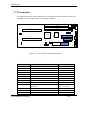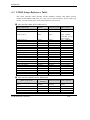
1
Introduction
AR-B1688
Full Size Dual
PIII CPU Card
User’s Guide
Edition : 1.1
Book Number : AR-B1688
AR-B1688 User’s Manual
1-1
Introduction
Table of Contents
How to Use This Manual
Chapter 1. Introduction
1-1 Check List............................................................................................1 – 2
1-2 Product Specifications .........................................................................1 – 3
1-3 System Architecture..........................................................................1 – 5
Chapter 2. Hardware Configuration Setting
2-1 Jumpers ................................................................................................2 – 1
2-2 Connectors ...........................................................................................2 – 4
Chapter 3. System Installation
3-1 Slot-1 Processor .................................................................................3 – 1
3-2 Main Memory.......................................................................................3 – 5
3-3 Installing the Single Board Computer............................................3 – 6
3-4 M-system Flash Disk .........................................................................3 – 6
3-5 Watch Dog Timer Programming.....................................................3 – 7
3-6 System Status Monitoring ................................................................3 – 8
Chapter 4. BIOS Setup Information
4-1
Entering Setup...................................................................................4 – 1
4-2
Main Menu..........................................................................................4 – 2
4-3 CMOS Setup Reference Table........................................................4 – 3
4-4 Standard CMOS Setup Menu..........................................................4 – 6
4-5 Advanced CMOS Setup Menu.........................................................4 – 6
4-6 Advanced Chipset Setup Menu........................................................4 – 8
4-7 Power Management Setup Menu................................................. 4 – 10
4-8 PCI/Plug and Play Setup Menu ................................................... 4 – 13
4-9 Peripheral Setup Menu................................................................. 4 – 15
4-10 Hardware Monitor Setup Menu................................................... 4 – 17
4-11 BIOS POST Check Point List.................................................... 4 – 17
4-12 Flash BIOS Utility ........................................................................... 4 – 22
AR-B1688 User’s Manual
1-2
Introduction
Chapter 5. Troubleshooting
5.1 Backplane Setup....................................................................................5 – 1
5.2 BIOS Setting ..........................................................................................5 – 4
5-3 OS Diagnostics.......................................................................................5 - 6
AR-B1688 User’s Manual
1-3
Introduction
How to Use This Manual
The manual describes how to configure your AR-B1688 system to meet various operating
requirements. It is divided into four chapters, with each chapter addressing a basic concept
and operation of Single Board Computer.
Chapter 1 : Introduction. presents what you have in the inside of box and give you an overview of the
product specifications and basic system architecture for this model of single board computer.
Chapter 2 : Hardware Configuration Setting. shows the definitions and locations of Jumpers
and Connectors that you can easily configure your system.
Chapter 3 : System Installation. describes how to properly mount CPU1 & CPU2, main
memory and M-system flash disk to get a safe installation and give you a programming guide
of Watch Dog Timer function.
Chapter 4 : BIOS Setup Information. specifies the meaning of each setup parameters and how
to get advanced BIOS performance and update new BIOS. In addition, POST checkpoint list
will give you a guide of trouble-shooting.
Chapter 5 : Troubleshooting. gives you a few reminding hints in building up a valid and
working system with AR-B1688, in terms of hardware and software perspective. Issues
addressed are based on the customer application history collected throughout the years, and
are presented as the most frequently encountered problems.
The content of this manual and EC declaration document is subject to change without prior
notice. These changes will be incorporated in new editions of the document. Portwell may
make supplement or change in the products described in this document at any time.
Updates to this manual, technical clarification, and answers to frequently asked questions will
be shown on the following web sit http://www.acrosser.com
AR-B1688 User’s Manual
1-4
Introduction
CHAPTER 1
Introduction
The AR-B1688 all-in-one single board computer is designed to fit a high performance
dual Pentium II or Pentium III based CPU and compatible for high-end computer
system with PCI Local Bus architecture. It is made to meet today’s demanding pace,
and keep complete compatibility with hardware and software designed for the IBM
PC/AT. It's beneficial to build up a high performance and high data availability
system for VARs, or system integrators. The on-board dual processors operation will
bring high performance to all segments of the PC, workstation, and server market.
This single board computer can run with dual Intel Pentium II or Pentium III
processor up to 550 MHz, and support DIMM up to 1GB DRAM. The enhanced
on-board PCI IDE interface can support 4 drives up to PIO mode 4 timing and Ultra
DMA/33 synchronous mode feature. The on-board Super I/O Chipset integrates
floppy controller, two serial ports, one FIR (Fast Infrared) port and one parallel port.
Two high performance 16C550-compatible UARTs provide 16-byte send/receive
FIFOs, and the multi-mode parallel port supports SPP/EPP/ECP function. Besides,
two USB (Universal Serial Bus) ports provide high-speed data communication
between peripherals and PC.
The PICMG standard makes the AR-B1688 works with the legacy ISA, ISA/PCI or
multi-slots PCI-bus backplane. The on-board 32-pin DIP socket supports M-system
Disk-On-Chip product up to 144MB. The Watch-Dog Timer function can monitor
your system status. Two 6-pin Mini-DIN connectors are provided to connect PS/2
Mouse and Keyboard. The on board Flash ROM is used to make the BIOS update
easier. Two standard 5-1/4” disk power connectors (4-pin) are reserved to directly
get more power energy for big power applications, and the additional 5-pin shrouded
connector is reserved for connecting Keyboard interface on the backplane. The
high precision Real Time Clock/calendar is built in to support Y2K for accurate
scheduling and storing configuration information. One 4-pin header is designed to
support ATX power function. All of these features make AR-B1688 excellent in
applications.
AR-B1688 User’s Manual
1-5
Introduction
1-1 Check List
The AR-B1688 package includes the following basic items accompany with this
manual.
l
l
l
l
One AR-B1688 single board computer.
Accessory 1 :
One 26-to-DSUB25 printer cable.
One FDC 34pin cable.
One IDE 40pin cable.
One 5-pin to 5-pin keyboard cable for back plane connection.
Accessory 1 all put inside 1 bag.
Accessory 2 :
One 4-pin ATX power control cable for back plane connection.
One CPU card backage put inside a blister bag.
Ten RED 2.54mm jumper hat put inside a bag.
Accessory 2 all put inside 1 bag.
Accessory 3 :One USB 10-pin Cable put inside a bag.(Different Option)
If any of these items is damaged or missed, please contact your vendor and save all
packing materials for future replacement and maintenance.
AR-B1688 User’s Manual
1-6
Introduction
1-2 Product Specifications
• Main processor
Intel Pentium II processors and Pentium III processors up to 550 MHz
◇ CPU bus clock : 66/100 MHz
◇ CPU core/bus clock ratio : x2 to x8
• BIOS
AMI system BIOS with 128KB Flash ROM to support DMI, PnP, Green function,
and ACPI (option)
• Main Memory
Four 168-pin DIMM sockets, supporting 3.3V SDRAM with parity/ECC function up
to 1GB (registered type)
• L2 Cache Memory
256KB/512KB PBSRAM built in Pentium-II or Pentium-III processor module
• Chipset
Intel 440BX AGPset
• Bus Interface
Follow PICMG standard (32-bit PCI and 16-bit ISA )
Fully complies with PCI bus specification V2.1
• PCI IDE Interface
Supports two enhanced IDE ports up to four HDD devices with PIO mode 4 and
Ultra DMA/33 mode transfer
• Floppy Drive Interface
Supports one FDD port up to two floppy drives and 5-1/4"(360K, 1.2MB), 3-1/2"
(720K, 1.2MB, 1.44MB, 2.88MB) diskette format and 3-mode FDD (option)
• Serial Ports
Support two high-speed 16C550 compatible UARTs with 16-byte T/R FIFOs
• IR Interface
Supports one 6-pin header for serial Fast/Standard Infrared wireless
communication
• Parallel Port
Supports one SPP, EPP/ECP bi-directional parallel port
AR-B1688 User’s Manual
1-7
Introduction
• USB Interface
Supports two USB (Universal Serial Bus) ports for high speed I/O peripheral
devices
• PS/2 Mouse and Keyboard Interface
Supports two 6-pin Mini-DIN connectors and one 5-pin shrouded connector for
PS/2 mouse, keyboard and backplane connection
• ATX Power Control Interface
One 4-pin header to support ATX power control with Modem Ring-On and WakeOn-LAN function
• Auxiliary I/O Interfaces
System reset switch, external speaker, Keyboard lock and HDD active LED
• Real Time Clock/Calendar (RTC)
Supports Y2K Real Time Clock/calendar with battery backup for 10-year data
retention
• Watchdog Timer
0.5,1,2,4,8,16,32,64 sec. time-out intervals by jumper setting or 255 intervals
from 0.5 min. to 254.5 min. by software programming
• Disk-On-Chip (DOC) Feature
Reserved one 32-pin socket for M-system Flash Disk up to 144MB
• System Monitoring Feature
Monitor system temperature, operating voltage, and fan status
• External Power Connector
Supports two standard 5-1/4” disk power connectors to enhance power driving
• Power Good
On-board power good generator with 300ms ∼ 500ms reset duration
• Physical and Environmental Requirements
◆
◆
◆
◆
◆
◆
◆
Outline Dimension (L X W) : 339.5mm (13.36”) X 121.5mm (4.78”)
Board Weight : 1.1 lb. (0.5kg)
PCB layout : 8 layer
Power Requirements : +5V @10A (typ.), +12V @180mA, -12V @30mA
Operating Temperature : 0℃ ∼ 60℃ (32℉ ∼ 140℉)
Storage Temperature : -20℃ ∼ 80℃
Relative Humidity : 5% ∼ 95%, non-condensing
AR-B1688 User’s Manual
1-8
Introduction
1-3 System Architecture
The following illustration of block diagram will show you how AR-B1688 gives you a
highly integrated dual processors solution. The most up-to-date system architecture
of AR-B1688 includes three main VLSI chips , 82443BX Host Bridge, 82371EB South
Bridge (PIIX4E), and 82093AA IOAPIC, to support Pentium II /III processors,
SDRAM with ECC function, PCI bus interface, APM, ACPI compliant power
management (option), USB port, SMBus communication, and Ultra DMA/33 IDE
Master. The on-board super I/O chip , W83977ATF, will support PS/2 Keyboard
/Mouse, two UARTs, FDC, Parallel and Infrared interface. AR-B1688 will provide user
more flexibility, stability, and reliability of application in a harsh environment.
Two CPU sockets on AR-B1688 component side adopt Slot-1 to support Pentium II
processors and Pentium III processors. The available processor must support dual
processors operation. When single CPU is mounted, it is necessary to mount the CPU
module on CPU1 slot-1 socket. For most of AR-B1688 applications, installing multiprocessor to get higher system performance than uni-processor is very popular.
The North Bridge 82443BX provides a completely integrated solution for the system
controller and data path components in a Pentium II processor and Pentium III
processor system. Its 64-bit GTL+ based host bus interface, optimized 64-bit DRAM
interface with ECC supports four 3.3V DIMMs at the maximum bus frequency of 100
MHz. The 32-bit PCI bus interface supports 4 PCI masters for external backplane
support.
The South Bridge, 82371EB PCI ISA IDE Xcelerator (PIIX4E), provides a highly
integrated multifunction PCI-to-ISA bridge solution for the best industry application
and interrupt handshaking for IOAPIC. It supports 2-channel dedicated Ultra DMA33 IDE master interfaces, full Plug-and-Play (PnP) compatibility, and Advanced
Programmable Interrupt Controller (APIC) interface. It also supports 2-port Universal
Serial Bus (USB) feature and PCI 2.1 compliance operation. It fully supports
Operating System Directed Power Management via the Advanced Configuration and
Power Interface (ACPI) specification. In addition, it also provides XD-bus via buffer
logic control to support BIOS read/write access, IOAPIC data access and external
real-time clock (RTC) to maintain time and date of a system.
The 82093AA I/O Advanced Programmable Interrupt Controller (IOAPIC) provides
multi-processor interrupt management and incorporates both static and dynamic
symmetric interrupt distribution across all processors in AR-B1688. While the
standard ISA Compatible interrupt controller (located in the PIIX4E) is intended for
use in a uni-processor system, the IOAPIC can be used in either a uni-processor or
multi-processor system. At the AR-B1688 system level, APIC consists of two parts
--- one residing in the I/O subsystem (called the IOAPIC) and the other in the CPU
AR-B1688 User’s Manual
1-9
Introduction
(called the Local APIC). The local APIC and the IOAPIC communicate over a
dedicated APIC bus.
The Super I/O chip W83977ATF integrates two high-speed serial ports, one parallel
port, FIR/SIR interface, FDD interface and 8042 keyboard controller with PS/2 mouse
ports. This parallel port supports one PC-compatible printer port (SPP), Enhanced
Parallel Port (EPP) and Extended Capabilities Port (ECP).
For standard PICMG form factor, a standard 16-bit ISA bus interface is applied for all
slower I/O operations. In AR-B1688, it contains watch-dog timer (WDT) enabled by
jumper setting and trigger by software, and disk-on-chip (DOC) for M-system Flash
disk. Besides, an advanced feature is used on AR-B1688 to support detecting and
monitoring of system temperature, operating voltage and fan status. The monitoring
message can be obtained from BIOS CMOS setup or running utility.
All of details of operating relations are shown in Figure 1-1 AR-B1688 System Block
Diagram.
AR-B1688 User’s Manual
1-10
Introduction
PWM1 (For CPU1)
Dual PENTIUM II/III
Processors (SLOT1)
CPU1 and CPU2
PWM2 (For CPU2)
CLOCK
GENERATOR
APIC Bus
CPU Bus
82443BX
1
2
MEMORY
4 SDRAM DIMM
3
( 492 BGA )
PIIX4E
4
PCI Bus
XD Bus
IOAPIC
82093AA
ULTRA 33 Dual Channel
IDE Bus Master
IDE 1
XD Bus
IDE 2
82371EB
( 324 BGA )
PIIX4E
TWO USB PORTS
CNTL
XD Bus
BIOS
BUFFER
LOGIC
SD Bus
Onboard
ISA Bus
RTC
SYSTEM MONITORING
ISA Bus
LM79
ISA Buffer
ISA Bus (Golden Finger)
WDT
DISK-On-Chip
KEYBOARD
MOUSE
SUPER I/O
W83977ATF
(128 PQFP)
2UART/LPT/FDD/IR
Figure 1-1 AR-B1688 System Block Diagram
AR-B1688 User’s Manual
1-11
Introduction
CHAPTER 2
Hardware Configuration Setting
This chapter gives the definitions and shows the positions of jumpers, headers and
connectors. All of the configuration jumpers on AR-B1688 are in the proper position.
The default settings shipped from factory are marked with a star ( * ).
2-1 Jumpers
In general, jumpers on the single board computer are used to select options for
certain features. Some of the jumpers are designed to be user-configurable, allowing
for system enhancement. The others are for testing purpose only and should not be
altered. To select any option, cover the jumper cap over (Short) or remove (NC) it
from the jumper pins according to the following instructions. Here NC stands for
“Not Connected”. (Please refer to Figure 2-1 for jumper positions)
DIMM1
JP1
DIMM2
CPU1
1
DIMM3
JP2
DIMM4
1
82443 BX
82371 EB
2
CPU2
SW1
1 JP3
1
1
1
31
JP4 JP5 JP6 JP7
Figure 2-1
AR-B1688 User’s Manual
2
1JP9 5
AR-B1688 Jumper
1-12
Introduction
CPU Jumper Setting Table (SW1)
SW1 DIP switch settings for CPU core/bus ratio
SW-1
SW-2
SW-3
SW-4
OFF
OFF
ON
OFF
OFF
OFF
OFF
OFF
ON
ON
ON
ON
ON
OFF
ON
ON
ON
ON
OFF
ON
ON
OFF
OFF
ON
ON
ON
ON
OFF
ON
OFF
ON
OFF
ON
ON
OFF
OFF
ON
OFF
OFF
OFF
OFF
ON
ON
ON
OFF
OFF
ON
ON
OFF
ON
OFF
ON
OFF
OFF
OFF
ON
OFF
ON
ON
OFF
OFF
ON
OFF
OFF
CORE/BUS RATIO
1.5x
2.0x
2.0x
2.5x
3.0x
3.5x
4.0x
*
4.5x
5.0x
5.5x
6.0x
6.5x
7.0x
7.5x
8.0x
Reserved
NOTE : For system stability, do not arbitrarily set CPU to run over speed
you can handle BIOS parameters.
Disk-On-Chip Jumper Setting (JP3)
1–2
Short
NC
NC
NC
3–4
NC
Short
NC
NC
5–6
NC
NC
Short
NC
7–8
NC
NC
NC
Short
Memory Address Window
D0000 – D1FFF *
D2000 – D3FFF
D4000 – D5FFF
D6000 – D7FFF
Watch-Dog Timer Jumper Setting (JP4, JP5, JP6, JP7, JP9)
JP4 NC : Enabled WDT function
Short : Disabled WDT function *
JP6 1 – 2 : Report to “RESET” when WDT time-out *
2 – 3 : Report to “NMI” when WDT time-out
AR-B1688 User’s Manual
1-13
unless
Introduction
JP9 Hardware WDT Time-out Interval (Twd) settings
5-6
3-4
1-2
Time-out Interval (Twd)
Short
Short
Short
0.5 sec.
Short
Short
NC
1 sec.
*
Short
NC
Short
2 sec.
Short
NC
NC
4 sec.
NC
Short
Short
8 sec.
NC
Short
NC
16 sec.
NC
NC
Short
32 sec.
NC
NC
NC
64 sec.
JP7
1 – 2 : Time-out period from H/W WDT *
2 – 3 : Time-out period from Super I/O (83977ATF) WDT
JP5
NC : Allocate I/O port 0533H/0033H for H/W WDT programming *
Short : Allocate I/O port 0543H/0343H for H/W WDT programming
RTC CMOS Clear Jumper Setting (JP1)
JP1
NC : Normal operation *
Short : Clear CMOS contents
NOTE : This CMOS clearing operation is only effective after setting CMOS RAM
CLEAR FUNCTION to enable state in BIOS Advanced Chipset Setup. It
can be done under system power on or off period.
SMI Source Jumper Setting (JP8)
JP8
1 – 2 : APIC SMI alert *
2 – 3 : PIIX4 SMI alert
AT/ATX Power Supply Selection (JP2)
JP2
1 – 2 : Select ATX power supply
2 – 3 : Select AT power supply *
AR-B1688 User’s Manual
1-14
Introduction
2-2 Connectors
I/O peripheral devices and Flash disk will be connected to these interface connectors
and DOC socket located on this single board computer.
J1
DIMM4
DIMM2
CPU1
J3
J2
DIMM3
J5
J7
1
J4
J6
DIMM1
J10
3
J9
J8
1 J12 3
82371EB
82443BX
J11
CPU2
J13
J14
J15
1
1
3
9
3
J23
1
J16
J17
J19
10 2
J20
BIOS
J21
DOC
1
J18
5
U20
J22
Figure 2-2 ACTI-688 Connector Locations
CONNECTOR
J1
J2
J3
J4
J5
J6
J7
J8
J9
J10, J21
J11
J12
J13
AR-B1688 User’s Manual
FUNCTION
System reset
External speaker interface
ATX power control interface
Wake-On-Lan (WOL) 3-pin connector
Infrared interface port
ATX power button interface
Keyboard lock
COM1 connector
IDE1/IDE2 access LED interface
Standard 5-1/4” disk drive power
connectors
IDE1 (Primary) interface
CPU1 FAN (+12V) power connector
PS/2 mouse connector
REMARK
Connect to Backplane
Connect to LAN card
6-pin Header
Connect to Chassis
Connect to Chassis
D-SUB9
4-pin connector
(pitch : 0.2 inch)
Connect to CPU1
6-pin Mini-DIN
1-15
Introduction
J14
J15
J16
J17
J18
J19
J20
J22
J23
U20
CPU1, CPU2
DIMM1 – 4
IDE2 (Secondary) interface
Floppy connector
COM2 connector
Parallel port connector
External keyboard interface
External USB interface
Chassis FAN connector
PS/2 keyboard connector
CPU2 FAN (+12V) power connector
DOC socket
Slot-1 for Pentium-II/III CPU
3.3V SDRAM DIMM socket
D-SUB9
Two ports
6-pin Mini-DIN
Connect to CPU2
M-system Flash Disk
Pin Assignments of Connectors
■ J1: Reset Header
PIN No.
1
2
Signal Description
Reset
Ground
■ J2 : External Speaker Header
PIN No.
1
2
3
4
Signal Description
Speaker signal
N/C
Ground
+5V
■ J7 : Keyboard Lock Header
PIN No.
1
2
3
4
5
Signal Description
+5V (330 ohm pull-up for power LED)
N/C
Ground
Keyboard inhibit
Ground
■ J3 : ATX Power Control Connector
PIN No.
Signal Description
1
ATX P/S Power Good Signal
2
ATX P/S 5V Standby Power
3
ATX P/S Power On Control
AR-B1688 User’s Manual
1-16
Introduction
4
AR-B1688 User’s Manual
Ground
1-17
Introduction
■ J9 : IDE1/IDE2 Access LED interface
PIN No.
1
2
Signal Description
+5V (330 ohm pull-up for HDD LED)
HDD Active # (LED cathode terminal)
■ J12 / J23 / J20 : CPU1 & CPU2 &Chassis Fan Power Input Connector
PIN No.
1
2
3
Signal Description
Ground
+12V
FAN_status (pull-up 5V)
■ J11 / J14 : IDE1/IDE2 Interface Connector
PIN No.
1
3
5
7
9
11
13
15
17
19
21
23
25
27
29
31
33
35
37
39
Signal Description
RESET#
Data 7
Data 6
Data 5
Data 4
Data 3
Data 2
Data 1
Data 0
Ground
DMA REQ
IOW#
IOR#
IOCHRDY
DMA ACK#
INT REQ
SA1
SA0
HDC CS0#
HDD Active#
AR-B1688 User’s Manual
PIN No.
2
4
6
8
10
12
14
16
18
20
22
24
26
28
30
32
34
36
38
40
Signal Description
Ground
Data 8
Data 9
Data 10
Data 11
Data 12
Data 13
Data 14
Data 15
N/C
Ground
Ground
Ground
Pull-down
Ground
N/C
N/C
SA2
HDC CS1#
Ground
1-18
Introduction
■ J10 / J21 : Standard 5-1/4” Disk Drive Power Connector
PIN No.
1
2
3
4
Signal Description
+12V
Ground
Ground
+5V
■ J15 : FDC Interface Connector
PIN No.
1
3
5
7
9
11
13
15
17
19
21
23
25
27
29
31
33
Signal Description
Ground
Ground
Ground
Ground
Ground
Ground
Ground
Ground
Ground
Ground
Ground
Ground
Ground
Ground
N/C
Ground
N/C
PIN No.
2
4
6
8
10
12
14
16
18
20
22
24
26
28
30
32
34
Signal Description
Density Select 0
N/C
Density Select 1
Index#
Motor ENA#
Drive Select B#
Drive Select A#
Motor ENB#
Direction#
Step#
Write Data#
Write Gate#
Track 0#
Write Protect#
Read Data#
Head Select#
Disk Change#
■ J4 : Wake-On-LAN (WOL) Interface Connector
PIN No.
1
2
3
AR-B1688 User’s Manual
Signal Description
5V Standby Power
Ground
LAN wake up signal
1-19
Introduction
■ J17 : Parallel Port Connector
PIN No. Signal Description
1
Strobe#
2
Data 0
3
Data 1
4
Data 2
5
Data 3
6
Data 4
7
Data 5
8
Data 6
9
Data 7
10
Acknowledge#
11
Busy
12
Paper Empty
13
Printer Select
PIN No.
14
15
16
17
18
19
20
21
22
23
24
25
26
Signal Description
Auto Form Feed#
Error#
Initialization#
Printer Select IN#
Ground
Ground
Ground
Ground
Ground
Ground
Ground
Ground
N/C
■ J5 : Fast & Standard IrDA Infrared Interface Port
PIN No.
1
2
3
4
5
6
Signal Description
VCC (+5V)
FIRRX (Reserved)
IRRX
Ground
IRTX
N/C
■ J8 / J16 : Serial Port D-SUB 9-PIN Connector
PIN No.
Signal Description
1
Data Carrier Detect (DCD)
2
Receive Data (RXD)
3
Transmit Data (TXD)
4
Data Terminal Ready (DTR)
5
Ground (GND)
6
Data Set Ready (DSR)
7
Request to Send (RTS)
8
Clear to Send (CTS)
9
Ring Indicator (RI)
AR-B1688 User’s Manual
1-20
Introduction
■ J19 : External USB Interface Connector
PIN No.
1
3
5
7
9
Signal Description
+5V
SBD0- (USBP0-)
SBD0+ (USBP0+)
Ground
N/C
PIN No.
2
4
6
8
10
Signal Description
N/C
Ground
SBD1+ (USBP1+)
SBD1- (USBP1-)
+5V
■ J13 : PS/2 Mouse Connector (6-pin Mini-DIN)
PIN No.
1
2
3
4
5
6
Signal Description
Mouse Data
N/C
Ground
+5V
Mouse Clock
N/C
■ J6 : ATX Power Button Interface
PIN No.
1
2
Signal Description
Power Button Control Signal
Pull down 1K ohm to ground
■ J18 : External Keyboard Connector
PIN No.
1
2
3
4
5
Signal Description
Keyboard Clock
Keyboard Data
N/C
Ground
+5V
■ J22 : PS/2 Keyboard Connector (6-pin Mini-DIN)
PIN No.
1
2
3
4
5
6
AR-B1688 User’s Manual
Signal Description
Keyboard Data
N/C
GND
+5V
Keyboard Clock
N/C
1-21
Introduction
CHAPTER 3
System Installation
This chapter provides you with instructions on how to set up and configure your
system. The additional information shows you how to install M-system Flash disk,
monitor system status, and handle WDT operation in software program.
3-1 Slot 1 Processor
Installing Pentium-II /III Processors
1). Mounting the Single Edge Contact (SEC) Cartridge or SECC2 CPU module:
Place the CPU cartridge from a vertical direction to the retention module and
gently slide it down the trails. Push the CPU cartridge gently but firmly until it is
fully inserted. You can install processor module into CPU1 and CPU2 slot out of
order. (Refer to Fig. 3-1 & Fig. 3-2)
2). Lock the CPU cooling fan power connector into dedicated 3-pin header. (Fig.33)
Fig. 3-1
AR-B1688 User’s Manual
1-22
Introduction
Fig. 3-2
Fig. 3-3
NOTICE
For SECC2 type CPU, please make sure that the two latches on both sides of the
retention module are moved up to firmly secure your PII CPU (Fig-3.4). The retention
module has been installed shipped and should not be removed for any reason as it is
required to firmly secure your PII/III CPU. Please apply your CPU on CPU 1 slot-1
socket for single CPU application.
AR-B1688 User’s Manual
1-23
Introduction
Fig. 3-4
Removing Pentium-II/III Processors
1). Remove the cooling fan power connector from the 3-pin header first.
2). Unmount the CPU Cartridge: Press the locks at both sides of the cartridge. Push
gently but firmly the CPU Cartridge out of the retention module. (Fig. 3-5, Fig. 36)
Fig. 3-5
AR-B1688 User’s Manual
1-24
Introduction
Fig. 3-6
NOTICE
Refer to Fig. 3-7 to remove SECC2 type CPU. Please move down the latch on both
sides of the retention module, and then gently slide out the CPU. Forcing the CPU
out without moving down the latches will break the retention module.
Fig. 3-7
AR-B1688 User’s Manual
1-25
Introduction
Fig. 3-8
Please refer to Fig.3-8 to mount the last PCBA retention mechanism. This will help to
secure the balance of AR-B1688 on backplane if system is installed in the chassis.
3-2 Main Memory
AR-B1688 provides four DIMMs (168-pin Dual In-line Memory Module) to support
3.3V SDRAM (Synchronized DRAM) as on-board main memory. The maximum
memory size is 1GB (registered type of SDRAM). For 66MHz system bus clock only
SDRAM with speed less than 100ns (-10) could be used. If you adopt 100MHz
system clock, you need to use SDRAM with speed less than 80ns (-8). You would
better use PC100-compliant memory chip.
For system compatibility and stability, don’t use memory module without brand. You
can also use the single or double-side DIMM with ECC feature. The four DIMMs can
be out of order. You can install different size of SDRAM module on DIMM1, DIMM2,
DIMM3, DIMM4 or all to boot up system.
Watch out the contact and lock integrity of memory module with socket, it will impact
on the system reliability. Follow normal procedure to install your DRAM module into
memory socket. Before locking, make sure that the module has been fully inserted
into the DIMM slot.
AR-B1688 User’s Manual
1-26
Introduction
NOTE : For maintaining system stability, don’t change any of DRAM parameters in
BIOS setup to upgrade your system performance without acquiring technical
information.
3-3 Installing the Single Board Computer
To install your AR-B1688 into standard chassis or proprietary environment, you need
to perform the following :
□
□
□
□
Step 1 : Check all jumpers setting on proper position
Step 2 : Install and configure CPUs and memory modules on right position
Step 3 : Place AR-B1688 into the dedicated position in your system
Step 4 : Attach cables to existing peripheral devices and secure it
WARNING
1). Please ensure that your SBC properly inserted and fixed by
mechanism. Otherwise, the system might be unstable or do not
work from bad contact of golden finger.
2). It is strongly recommended to run AR-B1688 by installing
dual processors to get good performance and stability.
Otherwise, if you only have one PII/III CPU, it is necessary to
mount the CPU over CPU1 slot-1.
3-4 M-system Flash Disk
AR-B1688 reserves one 32-pin DIP sockets for installing M-system Flash disk from
2MB to 144MB. This operation structure is running with pure ISA-bus without PnP
(Plug and Play) function. Before installing, make certain that memory window address
jumper setting is set on right position to prevent unworkable system due to memory
mapping I/O resource conflict. Do remember to follow DOC (DiskOnChip) installation
procedure. Otherwise, it is possible to burn out the Flash chip due to incorrect
installation.
Installing DOC
Align the DOC with pin holes on the socket. Make sure that the notched corner or
dot mark (pin 1) of DOC corresponds to notched corner of the socket. Then press the
DOC gently until it fits into place. If installation procedure is correct, the Flash disk
can be viewed as a normal hard disk to access read/write data.
WARNING : Please ensure that your DOC is properly inserted. Placing the DOC
in reverse will cause severe damage to it.
AR-B1688 User’s Manual
1-27
Introduction
The AR-B1688 will instruct user to install and utilize DOC for practical application. If
you want to boot from this Flash disk, it is necessary to refer to the application note
from M-system. You can easily get relatively advanced information or utility from Msystem shipping package (such as product manual) or Web-site http://www.msys.com.
3-5 Watch Dog Timer Programming
There are two manners to activate the WDT (Watch-Dog Timer) function. One is to
utilize hardware jumper setting and programmed by software command. The other
one is to program super I/O W83977 chip to start WDT counting. It is recommended
to use first methodology. The second choice is very difficult and complicated.
An optional two-port Watch-Dog Timer (WDT) is provided on AR-B1688. This
function can be enabled by jumper setting and software trigger, a system reset will be
generated unless the CPU triggers the timer periodically within time-out period. This
allows the system to restart in an orderly way in case of any abnormal condition is
found.
This WDT comes with 8 possible ranges of time intervals from 500 ms to 64 seconds,
which is adjustable by setting jumper positions. It could be enabled and programmed
by reading I/O port 0533H or 0543H to issue trigger continuously, and disabled by
reading I/O port 0033H or 0343H. A tolerance of 30% timer limit must be considered.
For instance, if the time-out interval is set to 1 second, the WDT trigger command
must be issued within 700ms at least.
The example below gives you a sample algorithm for WDT programming via I/O port
0533H and 0033H in your application program :
Enable WDT
MOV
IN
DX, 0533H
AL, DX
MOV
IN
DX, 0533H
AL, DX
MOV
IN
DX, 0033H
AL, DX
Re-trigger WDT
Disable WDT
NOTE : Please directly contact your technical specialist to get WDT programming
information on super I/O chip for long time-out interval support from 0.5
minutes to 254.5 minutes.
AR-B1688 User’s Manual
1-28
Introduction
3-6 System Status Monitoring
There are three manners to extract and monitor system environment message.
1). Reading system status from BIOS Hardware Monitor CMOS Setup. It can show
you current operating voltage, fan status, and system temperature.
2). Run LDCM utility under Windows environment. You can see the message display
operating voltage, fan status, system temperature, and system health on screen.
3). Run special utility based on LM79 to monitor system status under dedicated
Operating System. The smart functions could be user-defined and decided by
programmer.
AR-B1688 User’s Manual
1-29
Introduction
CHAPTER 4
BIOS Setup Information
AR-B1688 is equipped with the AMI BIOS stored in Flash ROM. This BIOS has a built-in
Setup program that allows users to modify the basic system configuration easily. This type
of information is stored in CMOS RAM so that it is retained during power-off periods. When
system is turned on, AR-B1688 communicates with peripheral devices and check its hardware
resources against the configuration information stored in the CMOS memory. If any error is
detected, or the CMOS parameters need to be initially defined, the diagnostic program will
prompt the user to enter the SETUP program. Some errors are significant enough to abort the
start-up.
4-1 Entering Setup
Turn on or reboot the computer. When the message “Hit <DEL> if you want to run
SETUP” appears, press <Del> key immediately to enter BIOS setup program.
If the message disappears before you respond, but you still wish to enter Setup,
please restart the system to try “COLD START” again by turning it OFF and
then ON, or touch the "RESET" button. You may also restart from “WARM
START” by pressing <Ctrl>, <Alt>, and <Delete> keys simultaneously. If
you do not press the keys at the right time and the system will not boot, an
error message will be displayed and you will again be asked to,
Press <F1> to Run SETUP or Resume
In HIFLEX BIOS setup, you can use the keyboard to choose among options or
modify the system parameters to match the options with your system. The table
below will show you all of keystroke functions in BIOS setup.
EDITING KEYS
<Tab>
←↑→↓
<Enter>
+ /–
<Esc>
<PgUp>
<PgDn>
<F2>/<F3>
<F10>
AR-B1688 User’s Manual
FUNCTION
Move to the next field
Move the next field to the left, above, right, or below
Select in the current field
Increments / Decrements a value
Close the current operation and return to previous level
Returns to the previous option
Advances to the next option
Select background color
Show “Save current settings and exit (Y/N)” in main menu
1-30
Introduction
4-2 Main Menu
Once you enter AR-B1688 AMI BIOS CMOS Setup Utility, the Main Menu
will appear on the screen. The Main Menu
allows you to select from eleven setup functions and two exit choices.
Use arrow keys to switch the items and press <Enter> key to accept or enter
the sub-menu.
AMI BIOS HIFLEX SETUP UTILITY-VERSION 1.21
(C) 1998 American Megatrends , Inc. All Rights Reserved
Standard CMOS Setup
Advanced CMOS Setup
Advanced Chipset Setup
Power Management Setup
PCI/Plug and Play Setup
Peripheral Setup
Hardware Monitor Setup
Change User Password
Change Supervisor Password
Auto-Detect Hard Disks
Auto Configuration with Optimal Settings
Auto Configuration with Fail Safe Settings
Save Settings and Exit
Exit Without Saving
Standard CMOS setup for changing time, date, hard disk type, etc.
ESC : Exit ↑↓: Sel
F2/F3 : Color
F10 : Save & Exit
NOTE : It is strongly recommended to reload Optimal
Setting if CMOS is lost or BIOS is updated.
AR-B1688 User’s Manual
1-31
Introduction
4-3 CMOS Setup Reference Table
This setup reference table includes all the Optimal, Failsafe, and Other options
setting in each BIOS setup item. It is very easy to cross reference. If you want to go
details, you can directly refer to item description in sub-section.
▓ ADVANCED CMOS SETUP DEFAULTS
BIOS Setup Items
Quick Boot
Optimal
Default
Enabled
Failsafe Default Other Options
Disabled
1st Boot Device
IDE-0
IDE-0
2nd Boot Device
3rd Boot Device
4th Boot Device
Try Other Boot Device
S.M.A.R.T. for Hard Disks
BootUp Num-Lock
PS/2 Mouse Support
System Keyboard
Primary Display
Password Check
Boot To OS/2 > 64MB
System BIOS Cacheable
C000, 16K Shadow
C400, 16K Shadow
C800, 16K Shadow
CC00, 16K Shadow
D000, 16K Shadow
D400, 16K Shadow
D800, 16K Shadow
DC00, 16K Shadow
Floppy
CDROM
ATAPI ZIP
Yes
Disabled
On
Enabled
Absent
Absent
Setup
No
Enabled
Cached
Cached
Disabled
Disabled
Disabled
Disabled
Disabled
Disabled
Floppy
CDROM
ATAPI ZIP
Yes
Disabled
On
Enabled
Absent
Absent
Setup
No
Disabled
Cached
Cached
Disabled
Disabled
Disabled
Disabled
Disabled
Disabled
IDE-1, IDE-2, IDE3,
Floppy, CDROM,
ATAPI ZIP, LS-120,
SCSI, Network
IDE-1,…,CDROM
IDE-1,…,ATAPI ZIP
IDE-1,…,CDROM
No
Enabled
Off
Disabled
Present
VGA/EGA,…,Mono
Always
Yes
Enabled, Disabled
Enabled, Disabled
Cached, Enabled
Cached, Enabled
Cached, Enabled
Cached, Enabled
Cached, Enabled
Cached, Enabled
▓ ADVANCED CHIPSET SETUP DEFAULTS
BIOS Setup Items
Optimal
Default
Configure SDRAM Timing by
Disabled
SPD
SDRAM RAS# to CAS# delay
3 SCLKs
SDRAM RAS# Precharge
3 SCLKs
SDRAM CAS# Latency
3 SCLKs
SDRAM Leadoff Cmd Timing
Auto
AR-B1688 User’s Manual
Failsafe Default
Other Options
Disabled
Enabled
3 SCLKs
3 SCLKs
3 SCLKs
Auto
2
2
2
4
SCLKs
SCLKs
SCLKs
SCLKs, 3 SCLKs
1-32
Introduction
DRAM Integrity Mode
Non-ECC
Non-ECC
DRAM Refresh Rate
15.6 us
15.6 us
Memory Hole
Disabled
Disabled
8bit I/O Recovery Time
1 Sysclk
1 Sysclk
16bit I/O Recovery Time
1 Sysclk
1 Sysclk
AR-B1688 User’s Manual
EC-Only, ECC H/W
31.2 us, 62.4 us,
124.8 us, 249.6 us
512KB-640KB,
15MB-16MB
Disabled, 2, 3, 4, 5,
6, 7, 8 Sysclk
Disabled,2,3,4 Sysclk
1-33
Introduction
USB Passive Release
PIIX4 Passive Release
BIOS Setup Items
Enabled
Enabled
Optimal
Default
Disabled
Disabled
0.25%
Disabled
Enabled
PIIX4 Delayed Transaction
Spread Spectrum Control
Spread Spectrum Modulation
USB Function
USB Keyboard Legacy Support
CMOS
RAM
CLEAR
Disabled
FUNCTION
Enabled
Enabled
Disabled
Disabled
Failsafe Default Other Options
Disabled
Disabled
0.25%
Disabled
Enabled
Enabled
Enabled
0.5%
Enabled
Disabled
Disabled
Enabled
▓ POWER MANAGEMENT SETUP DEFAULTS
Power Management / APM
Green PC Monitor Power State
Video Power Down Mode
Hard Disk Power Down Mode
Optimal
Default
Enabled
Off
Disabled
Disabled
Standby Time Out (Minute)
Disabled
Disabled
Suspend Time Out (Minute)
Disabled
Disabled
Throttle Slow Clock Ratio
50 – 62.5%
50 – 62.5%
Display Activity
Device 6 (Serial Port 1)
Device 7 (Serial Port 2)
Device 8 (Parallel Port)
Device 5 (Floppy disk)
Device 0 (Primary master IDE)
Device 1 (Primary slave IDE)
Device 2 (Secondary master IDE)
Device 3 (Secondary slave IDE)
Power Button Function
Ring Resume From Soft Off
Ignore
Monitor
Monitor
Ignore
Monitor
Monitor
Ignore
Monitor
Ignore
Suspend
Disabled
Ignore
Monitor
Monitor
Ignore
Monitor
Monitor
Ignore
Monitor
Ignore
Suspend
Disabled
BIOS Setup Items
Failsafe Default
Disabled
Off
Disabled
Disabled
Other Options
Stand By, Suspend
Stand By, Suspend
Stand By, Suspend
1, 2, 4, 8, 10, 20, 30,
40, 50, 60 Min.
1, 2, 4, 8, 10, 20, 30,
40, 50, 60 Min.
0-12.5%, 12.5-25%,
25-37.5%,
37.550%,
62.5-75%, 75-87.5%
Monitor
Ignore
Ignore
Monitor
Ignore
Ignore
Monitor
Ignore
Monitor
On / Off
Enabled
▓ PCI / PnP SETUP DEFAULTS
Optimal
Default
BIOS Setup Items
Plug and Play Aware O/S
Clear NVRAM
Failsafe Default
No
No
No
No
PCI Latency Timer (PCI Clocks) 64
64
AR-B1688 User’s Manual
Other Options
Yes
Yes
32, 96, 128, 160,
192,
224, 248
1-34
Introduction
PCI VGA Palette Snoop
Allocate IRQ to PCI VGA
PCI IDE BusMaster
Disabled
Yes
Disabled
Disabled
Yes
Disabled
OffBoard PCI IDE Card
Auto
Auto
OffBoard PCI IDE Primary IRQ
Disabled
Disabled
OffBoard PCI IDE Secondary
Disabled
IRQ
Disabled
AR-B1688 User’s Manual
Enabled
No
Enabled
Slot1, Slot2, Slot3,
Slot4
INTA, INTB, INTC,
INTD, Hardwired
INTA, INTB, INTC,
INTD, Hardwired
1-35
Introduction
PCI Slot1 IRQ Priority
PCI Slot2 IRQ Priority
PCI Slot3 IRQ Priority
PCI Slot4 IRQ Priority
BIOS Setup Items
DMA Channel 0
DMA Channel 1
DMA Channel 3
DMA Channel 5
DMA Channel 6
DMA Channel 7
IRQ3
IRQ4
IRQ5
IRQ7
IRQ9
IRQ10
IRQ11
IRQ12
IRQ14
IRQ15
Auto
Auto
Auto
Auto
Optimal
Default
PnP
PnP
PnP
PnP
PnP
PnP
PCI/ PnP
PCI/ PnP
PCI/ PnP
PCI/ PnP
PCI/ PnP
PCI/ PnP
PCI/ PnP
PCI/ PnP
PCI/ PnP
PCI/ PnP
Auto
Auto
Auto
Auto
3,
3,
3,
3,
4,
4,
4,
4,
5,
5,
5,
5,
7,
7,
7,
7,
9,
9,
9,
9,
10,
10,
10,
10,
11
11
11
11
Failsafe Default Other Options
Pnp
Pnp
Pnp
Pnp
Pnp
Pnp
PCI/
PCI/
PCI/
PCI/
PCI/
PCI/
PCI/
PCI/
PCI/
PCI/
PnP
PnP
PnP
PnP
PnP
PnP
PnP
PnP
PnP
PnP
ISA/ EISA
ISA/ EISA
ISA/ EISA
ISA/ EISA
ISA/ EISA
ISA/ EISA
ISA/ EISA
ISA/ EISA
ISA/ EISA
ISA/ EISA
ISA/ EISA
ISA/ EISA
ISA/ EISA
ISA/ EISA
ISA/ EISA
ISA/ EISA
▓ PERIPHERAL SETUP DEFAULTS
OnBoard FDC
Optimal
Default
Auto
OnBoard Serial PortA
Auto
Auto
OnBoard Serial PortB
Auto
Auto
OnBoard IR Port
Disabled
Disabled
IR Mode Select
IR IRQ Select
IR DMA Select
N/A
N/A
N/A
N/A
N/A
N/A
OnBoard Parallel Port
Auto
Auto
BIOS Setup Items
AR-B1688 User’s Manual
Failsafe Default
Auto
Other Options
Enabled, Disabled
3F8h/COM1,
2F8h/COM2,
3E8h/COM3,
2E8h/COM4,
Disabled
3F8h/COM1,
2F8h/COM2,
3E8h/COM3,
2E8h/COM4,
Disabled
3F8h/COM1,
2F8h/COM2,
3E8h/COM3,
2E8h/COM4, Auto
IrDA, ASK-IR, FIR
3, 4, 5, 9, 10, 11, 12
0, 1, 3
Disabled,
378h,
278h,
3BCh
1-36
Introduction
Parallel Port Mode
EPP Version
Parallel Port IRQ
Parallel Port DMA Channel
Bi-Dir
N/A
Auto
N/A
Bi-Dir
N/A
Auto
N/A
OnBoard IDE
Both
Both
AR-B1688 User’s Manual
EPP, ECP, Normal
1.7 , 1.9
5, 7
0, 1, 3
Primary, Secondary,
Disabled
1-37
Introduction
4-4 Standard CMOS Setup Menu
This setup page includes all the items in a standard compatible BIOS. Use the
arrow keys to highlight the item and then use the <PgUp>/<PgDn> or <+>/<->
keys to select the value or number you want in each item and press <Enter> key to
certify it.
Follow command keys in CMOS Setup table to change Date, Time, Drive type, and
Boot Sector Virus Protection Status.
4-5 Advanced CMOS Setup Menu
This setup includes all of the advanced features in the system. The detail descriptions
are specified as belows.
Quick Boot
Set “Disabled” for normal booting or select “Enabled” to skip minor BIOS test items to
obtain quick boot response.
Boot Up Sequence
This category includes six items to determine which drive computer searches first
for the Disk Operating System (DOS).
The default ARMD (ATAPI Removable Media Device) emulation type is set to
popular drive type LS-120 and ATAPI ZIP. There are many choices of booting devices
to boot up system. User can select “Disabled”, “IDE-0”, “IDE-1”, “IDE-2”, “IDE3”, “Floppy”, “LS-120”, “ATAPI ZIP”, “CDROM”, “SCSI”, or “NETWORK”.
Boot Up Num-Lock
Select “On” to enable numeric function of the numeric keypad, or “Off” to disregard it.
PS/2 Mouse Support
Select “Enabled” to enable PS/2 mouse function, or “Disabled” to release IRQ12
interrupt for other ISA-bus I/O devices.
AR-B1688 User’s Manual
1-38
Introduction
System Keyboard
This option will be used to neglect “keyboard error” while you choose Absent setting
in your BIOS setup and system has no keyboard attached.
Primary Display
Chooses Absent, VGA/EGA, CGA40x25, CGA80x25, or Mono to meet your monitor
type. If you select Absent, the “CMOS Display Type Wrong” message will be ignored
regardless the mismatched display card.
Password Check
This option enables the password checking when the system boots up or runs CMOS
Setup. It only takes effect after setting Change Supervisor Password.
Setup : This option will force system to check password before running Setup if you
have already entered the current user password in “Change User Password”.
By that time, the system will be only able to boot but deny accessing Setup.
Always : Password prompt appears every boot-up. The system will not boot and deny
access Setup with invalid password. The best way is to clear CMOS or try to
reload BIOS Setup to boot up system.
Boot To OS/2 > 64MB
You should set this option to “Yes” to support OS/2 environment.
System BIOS Cacheable
Enables this option to enhance system performance by shadowing and caching
system BIOS. When disabled, this BIOS shadow function will be ignored.
Video BIOS Shadow
Select “Cached” option to get more higher display performance by shadowing and
caching VGA BIOS. If user chooses “Enabled” option, only BIOS shadow function is
active. The “Disabled” option will ignore this BIOS caching and shadowing function.
AR-B1688 User’s Manual
1-39
Introduction
Shadow Memory (from address C000 – DFFF, 16K per segment)
Each of segments provides three options “Disabled”, “Enabled”, and “Cached” for
faster adapter’s ROM execution. However this shadow function is Chipset oriented
and dependent on system hardware feature. In general, C000 and C400 will be allocated
for VGA BIOS and set to Cached to get higher display performance by shadowing and
caching feature. If user chooses Enabled setting, only BIOS shadow function is active.
4-6 Advanced Chipset Setup Menu
This setup is very important to keep system stability. If you are not technical person,
do not attempt to change any parameters. The best way is to choose optimal default
setting.
Configure SDRAM Timing by SPD
This option provides DIMM plug-and-play support by Serial Presence Detect (SPD)
mechanism via the System Management Bus (SMBus) interface. You can disable this
option to manage the following four SDRAM timing options by yourself. In addition,
SDRAM operating timings may follow serial presence from EEPROM content by
setting this option to “Enabled”, and all of SDRAM timing options will be not
available and hidden.
SDRAM RAS# to CAS# delay
This option controls the number of SCLKs (SDRAM Clock) from a row activate
command to a read or write command. If your system installs good quality of SDRAM,
you can set this option to “2 SCLKs” to obtain better memory performance. Normally,
the option will be set to 3 SCLKs.
SDRAM RAS# Precharge
This option controls the number of SCLKs for RAS# precharge. If your system installs
good quality of SDRAM, you can set this option to “2 SCLKs” to obtain better
memory performance.
AR-B1688 User’s Manual
1-40
Introduction
SDRAM CAS# Latency
This option controls the number of SCLKs between the time a read command is
sampled by the SDRAMs and the time the North Bridge, 82443BX, samples
correspondent data from the SDRAMs. For a registered DIMM with CAS# Latency =
2, this option should be set to “2 SCLKs” to acquire better memory performance.
SDRAM Leadoff Cmd Timing
This option is used to control when the SDRAM command pins (SRASx#, SCASx#
and Wex#) and CSx# are considered valid on leadoffs for CPU cycles. If you select
Auto, this timing will be automatically initialized and set by BIOS from CPU speed
detection. For Desktop platforms, it might be set to 4 SCLKs. In general, another
option 3 SCLKs will be set to meet Mobile platforms.
DRAM Integrity Mode
There are three options Non-ECC, EC-Only (Error Check Only) and ECC Hardware
(Error Checking and Correction) in this feature. The DRAM integrity mode will be
implemented by the parity algorithm when this option is set to “Non-ECC”.
DRAM Refresh Rate
This option specifies the refresh rate frequency for the installed system memory
SDRAM DIMMs. If you have good quality of DRAM, you can choose longer
refresh rate to get better system performance.
Memory Hole
This option allows the end user to specify the location of a memory hole for memory
space requirement from ISA-bus cards.
8bit I/O Recovery Time
This option specifies the length of the delay (in SYSCLKs) inserted between
consecutive 8-bit I/O operations.
16bit I/O Recovery Time
This option specifies the length of the delay (in SYSCLKs) inserted between
consecutive 16-bit I/O operations.
AR-B1688 User’s Manual
1-41
Introduction
USB Passive Release
When enabled, this allows PIIX4 to use Passive Release to obtain better USB
performance while transferring control information or data for USB transactions. When
disabled, PIIX4 will perform PCI accesses for USB without using Passive Release.
PIIX4 Passive Release
Choose the “Enabled” option to help raise the available bandwidth of the PCI bus for
acquiring higher PCI bus performance.
Spread Spectrum Control & Modulation
These two options are for EMI test issue only.
PIIX4 Delayed Transaction
Choose the “Enabled” option to obtain higher PCI bus performance for slower ISA
bus application.
USB Function
This option will enable on-chip USB function to support USB (Universal Serial Bus)
peripheral devices if user chooses the “Enabled” setting.
USB Keyboard Legacy Support
This feature will be automatically disabled and hidden if user chooses the “Disabled”
setting from the foregoing USB Function option. Otherwise, enabling this option
provides support for USB-keyboard without auxiliary driver under DOS environment.
CMOS RAM CLEAR FUNCTION
If your system supports Y2K RTC, you should set this option to Enabled to support
hardware CMOS clearing operation.
AR-B1688 User’s Manual
1-42
Introduction
4-7 Power Management Setup Menu
This APM (Advanced Power Management) determines how much power energy can
be saved by setting below items to handle system power resource. The following
descriptions will specify the definition of each item in details.
Power Management/APM
Using this feature to control system power resources. Set this option to “Enabled” to
enable power management function and effective based on following parameter
settings.
Green PC Monitor Power State
This option is used to decide what kind of power states are effective. There are three
options “Stand By”, “Suspend”, and “Off” in this feature. The “Stand By” option is
to turn off light power by handling of Monitor signals. The other “Suspend” mode is
to turn off heavy power. And the other one, “Off” state, is really to turn off the power
of the monitor.
Video Power Down Mode
This option specifies the power conserving state that the VESA VGA video subsystem
enters after the specified period of display inactivity has expired.
Hard Disk Power Down Mode
This option specifies the power management state that the HDD enters after the
specified period of hard drive inactivity has expired. It is the same as video power
control. If user chooses “Stand By” or “Suspend”, it will depend on period of
parameter “Stand By Time out”or “Suspend Time out”.
Stand by Time out (Minute)
This option specifies the length of the period of system inactivity while the computer
is in Full-On power state before the computer is placed in Standby mode.When this
length of time expires, the computer enters Standby Timeout state. In Standby mode,
some power use is curtailed.
AR-B1688 User’s Manual
1-43
Introduction
Suspend Time out (Minute)
This option is the same as Stand by Time out function. These two features will be
enabled to monitor power of sub-items “Display Activity”, “Serial port”, “Parallel
Port”, “Floppy”, “Pri-HDD”, and “Sec-HDD” independently. It is also used to
control CPU throttle running function. All of sub-items will be ineffective in selection
of disabling “Stand by Time out” or “Suspend Time out” even if it can be choosed by
user in BIOS setup menu.
Throttle Slow Clock Ratio
This option specifies the speed at which the system clock runs in power saving
modes. The settings are expressed as duty cycle of the STPCLK# signal. This duty
cycle indicates the percentage of time the STPCLK# signal is asserted while in the
throttle mode.
Display Activity
This option specifies if BIOS is to monitor activity on the display monitor for power
conservation purposes. If set to Monitor and the computer is in a power saving state,
BIOS watches for video display activity. The computer enters the full on power state if
any activity occurs. BIOS reloads the Standby and Suspend timeout timers if activity
occurs on the specified IRQ lines. If set to Ignore, video display monitor activity is not
monitored.
Device 6/7/8/5/0/1/2/3 (Serial 1&2, Parallel, FDD, Pri/Sec HDD)
When set to Monitor, these options enable event monitoring on the specified
hardware device. If set to Monitor and the computer is in a power saving state, BIOS
watches for activity on the device with specified IRQ line. The computer enters the full
on power state if any activity occurs. BIOS reloads the Standby and Suspend timeout
timers if activity occurs on the specified device. No monitoring activity occurs if the
option is set to Ignore. The settings for each of these options are Monitor or Ignore.
Power Button Function
This item is used to handle soft power on/off regardless of time counting (generally
speaking, it is 4 sec) if you set it to On/Off. You can easily power on/off system by
pressing power button (toggle switch) directly. This feature is only available on
system with ATX power control interface. If you use standard AT power supply, this
option will be ignored. However choose the “Suspend” setting , system will be forced
into suspend mode when user turn it off unless you can consecutively press the
power button for more than 4 second to get in Soft off function.
AR-B1688 User’s Manual
1-44
Introduction
Ring Resume From Soft Off
This item will be used to wake up system from remote ringing control under Soft Off
condition. If you choose “Disabled” setting, the system will be not resumed by
modem ring.
4-8 PCI/Plug and Play Setup
This section describes configuring the PCI bus system. PCI (Peripheral Component
Interconnect) is a system which allows I/O devices to operate at speeds nearing
CPU’s when they communicate with own special components.
All of options described in this section are important and technical and it is strongly
recommended that only experienced users could make any changes to the default
settings.
Plug and Play Aware O/S
Set this option to “Yes” if the operating system installed in the computer is Plug and
Play-aware. BIOS only detects and enables PnP ISA adapter cards that are required for
system boot. The Windows 95 operating system detects and enables all other PnPaware adapter cards. Windows 95 is PnP-aware. Set this option to “No” if the
operating system (such as DOS, OS/2, Windows 3.x) does not use PnP.You must set
this option correctly or PnP-aware adapter cards installed in your computer will not
be configured properly.
Clear NVRAM
This option is used to clear NVRAM and check or update ESCD (Extended System
Configuration Data) data after system power on. Set this option to No that will not
clear NVRAM and the operation of update ESCD is effective in different ESCD data
comparision. If you select the “Yes” setting, then the BIOS will update ESCD each
time of power on.
PCI Latency Timer (PCI Clocks)
This option is used to control PCI latency timer period (follow PCI clocks). Based on
PCI specification 2.1 or later and PCI bus frequency in system, user can select different
timer to meet their PCI bus environment.
AR-B1688 User’s Manual
1-45
Introduction
PCI VGA Palette Snoop
Some display cards that are non-standard VGA such as graphics accelerations or
MPEG video cards may not show colors properly. User can choose “Enabled”
setting to correct this display mismatch problem and support any ISA adapter card
installed in the computer requires VGA palette snooping.
Allocate IRQ to PCI VGA
This option will be used to allocate IRQ for PCI VGA card. In general, some of PCI
VGA cards need IRQ support.
PCI IDE BusMaster
Set this option to Enabled to specify that the IDE controller on the PCI local bus has
bus mastering capability.
Off Board PCI IDE Card
This option specifies if an offboard PCI IDE controller adapter card is used in the
computer. You must also specify the PCI expansion slot on the SBC (Single Board
Computer) where the offboard PCI IDE controller card is installed. If an offboard PCI
IDE controller is used, the onboard IDE controller on the SBC is automatically
disabled. If Auto is selected, BIOS automatically determines the correct setting for this
option. If you want to respectively control off board PCI IDE Primary/ Secondary IRQ
resources, you should set this option among Slot 1 to Slot 4. Otherwise, all of these
sub-options will be not available and hidden.
Off Board PCI IDE Primary/Secondary IRQ
This option specifies the PCI interrupt used by the primary/ secondary IDE channel on
the offboard PCI IDE controller. The settings are Disabled, INTA, INTB, INTC, INTD,
or Hardwired for installing off-board non-compliant PCI IDE card.
PCI Slot 1/2/3/4 IRQ Priority
These options specify the priority IRQ to be used for any PCI devices installed in
PCI expansion slots 1 through 4. The settings are Auto (AMIBIOS automatically
Determines the priority IRQ), (IRQ) 3, 4, 5, 7, 9, 10, or 11.
AR-B1688 User’s Manual
1-46
Introduction
DMA Channel 0/1/3/5/6/7
These options specify if the named DMA channel is available for using on the
ISA/EISA bus or PnP (Plug & Play).
IRQ 3/4/5/7/9/10/11/12/14/15
These options specify the bus that the named interrupt request lines (IRQs) are used
on. These options allow you to specify IRQs for use by legacy ISA adapter cards.
These options determine if AMIBIOS should remove an IRQ from the pool of available
IRQs passed to devices that are configurable by the system BIOS. The available IRQ
pool is determined by reading the ESCD NVRAM. If more IRQs must be removed from
the pool, the end user can use these PCI/PnP Setup to remove the IRQ by assigning
the option to the ISA/EISA setting. All IRQs used by on-board I/O are configured as
PCI/PnP.
4-9 Peripheral Setup
This section describes I/O resources assignment for all of on-board peripheral devices.
On Board FDC
If user wants to install different add-on super I/O card to connect floppy drives, set
this field to Disabled. Otherwise, set it to Auto to call BIOS to automatically
determine if the floppy controller should be enabled.
On Board Serial Port A/Port B
These fields control the resource assignments of two on-board serial interfaces SIO1
and SIO2.The following lists show current options in On Board Serial Port A/ Port B :
Auto à cannot set serial I/O resources by manual operation
Disabled à indicates on-board COM port function is ineffective
3F8h/COM1 à assign I/O address 3F8h to COM1
2F8h/COM2 à assign I/O address 2F8h to COM2
3E8h/COM3 à assign I/O address 3E8h to COM3
2E8h/COM4 à assign I/O address 2E8h to COM4
On Board IR Port
This option control the resource assignments of on-board serial port 3. The IR Mode
Select has three settings IrDA, ASK IR, and FIR.
AR-B1688 User’s Manual
1-47
Introduction
On Board Parallel Port
There are four optional items Parallel Port Mode, EPP Version, Parallel Port IRQ,
and Parallel Port DMA Channel used to control on-board parallel port interface while
user select I/O base address manually. The following lists are available options of
on-board parallel port :
Auto à user can not control all of LPT port I/O resources
Disabled à on-board parallel port function is ineffective and N/A
378h à locate IRQ7 for this default I/O address
278h à assign this I/O address to LPT1
3BCh à assign this I/O address to LPT1
◎ Parallel Port Mode :
This option specifies the parallel port mode. ECP and EPP are both bidirectional
data transfer schemes that adhere to the IEEE P1284 specifications. This Parallel
Port Mode includes four options “Normal”, “Bi-Dir”, “EPP”, and “ECP”.
Setting
Description
Normal Uni-direction operation at normal speed
Bi-Dir Bi-direction operation at normal speed
The parallel port can be used with devices that adhere to the
Enhanced Parallel Port (EPP) specification. EPP uses the
EPP
existing parallel port signals to provide asymmetric bidirectional
data transfer driven by the host device.
The parallel port can be used with devices that adhere to the
Extended Capabilities Port (ECP) specification. ECP uses the
ECP DMA protocol to achieve data transfer rates up to 2.5 Megabits
per second. ECP provides symmetric bidirectional
communication.
◎ EPP Version :
This option is only valid if the Parallel Port Mode option is set to EPP. This
option specifies the version of the Enhanced Parallel Port specification that will be
used by AMIBIOS.
◎ Parallel Port IRQ :
This option is only valid if the Onboard Parallel Port option is not set to Disabled.
This option sets the IRQ used by the parallel port.
◎ Parallel Port DMA Channel :
This option is only available if On Board Parallel Port is set to fixed I/O address
and the setting of Parallel Port Mode is ECP. This option sets the DMA channel
used by ECP-capable parallel port.
AR-B1688 User’s Manual
1-48
Introduction
On Board IDE
This option specifies the onboard IDE controller channels that will be used. The
settings are Disabled, Primary, Secondary, or Both.
4-10 Hardware Monitor Setup
This setup describes current system status detected from hardware monitor controller.
The status showed on screen will include :
l Current System Temperature (Generally indicates the inside temperature of
chassis or surface temperature of SBC)
l Current CPU1 Fan Speed
l Current CPU2 Fan Speed
l Current Chassis Fan Speed
l System operating voltage includes “CPU1 Vcore”, “Vtt”, “Vcc3”, +5V”, “+12V”,
“-12V”, and “-5V”.
4-11 BIOS POST Check Point List
AMIBIOS provides all IBM standard Power On Self Test (POST) routines as well as
enhanced AMIBIOS POST routines. The POST routines support CPU internal
diagnostics. The POST checkpoint codes are accessible via the Manufacturing Test
Port (I/O port 80h).
Whenever a recoverable error occurs during the POST, the system BIOS will display
an error message describing the message and explaining the problem in detail so that
the problem can be corrected.
During the POST, the BIOS signals a checkpoint by issuing one code to I/O address
80H. This code can be used to establish how far the BIOS has executed through the
power-on sequence and what test is currently being performed. This is done to help
troubleshoot faulty system board.
If the BIOS detects a terminal error condition, it will halt the POST process and
attempt to display the checkpoint code written to port 80H. If the system hangs
before the BIOS detects the terminal error, the value at port 80H will be the last
test performed. In this case, the terminal error cannot be displayed on the screen.
The following POST checkpoint codes are valid for all AMIBIOS products with a
core BIOS date of 07/15/95 version 6.27 (Enhanced).
Uncompressed Initialization Codes — The uncompressed initialization
checkpoint hex codes are listed in order of execution :
AR-B1688 User’s Manual
1-49
Introduction
Code
D0
D1
D3
D4
D5
D6
D7
D8
D9
Description
NMI is disabled. CPU ID saved. INIT code checksum verification will be
started.
Initializing the DMA controller, performing the keyboard controller BAT
test, starting memory refresh, and going to 4GB flat mode.
To start memory sizing.
Returning to real mode. Executing any OEM patches and setting the stack
next.
Passing control to the uncompressed code in shadow RAM at E000:0000h.
The INIT code is copied to segment 0 and control will betransferred to
segment 0.
Control is in segment 0. Next, checking if <Ctrl><Home> was pressed
and
verifying the system BIOS checksum.
If either <Ctrl><Home> was pressed or the system BIOS checksum is bad,
next will go to checkpoint code E0h.
Otherwise, going to checkpoint code D7h.
To pass control to interface module.
Main BIOS runtime code is to be decompressed.
Passing control to the main system BIOS in shadow RAM next.
Bootblock Recovery Codes — The bootblock recovery checkpoint hex codes
are listed in order of execution :
Code
E0
E1
E2
E6
ED
EE
EF
F0
F1
F2
F3
F4
F5
FB
Description
The onboard floppy controller if available is initialized. Next, beginning the
base 512KB memory test.
Initializing the interrupt vector table next.
Initializing the DMA and Interrupt controllers next.
Enabling the floppy drive controller and Timer IRQs. Enabling internal cache
memory.
Initializing the floppy drive.
Start looking for a diskette in drive A: and read first sector of the diskette.
A read error occurred while reading the floppy drive in drive A: .
Next, searching for the AMIBOOT.ROM file in the root directory.
The AMIBOOT.ROM file is not in the root directory.
Next, reading and analyzing the floppy diskette FAT to find the clusters
occupied by the AMIBOOT.ROM file.
Start reading AMIBOOT.ROM file, cluster by cluster.
The AMIBOOT.ROM file is not the correct size.
Next, disabling internal cache memory.
Next, detecting the type of Flash ROM.
AR-B1688 User’s Manual
1-50
Introduction
FC
FD
FF
Erasing the Flash ROM.
Programming the Flash ROM
Flash ROM programming was successful. Next, restarting the system BIOS.
AR-B1688 User’s Manual
1-51
Introduction
Uncompressed Initialization Codes — The following runtime checkpoint hex
codes are listed in order of execution. These codes are uncompressed in F0000h
shadow RAM.
Code
Description
03
05
06
07
08
The NMI is disabled. Next, checking for a soft reset or a power on condition.
The BIOS stack has been built. Next, disabling cache memory.
Uncompressing the POST code next.
Next, initializing the CPU and the CPU data area.
The CMOS checksum calculation is done next.
Next, performing any required initialization before the keyboard BAT
command is issued.
The keyboard controller input buffer is free. Next, issuing the BAT
command to the keyboard controller.
The keyboard controller BAT command result has been verified. Next,
performing any necessary INIT after the K/B controller BATcommand test.
The keyboard command byte is written next.
Next, issuing the pin 23 and 24 blocking and unblocking commands.
Next, checking if the <End> or <Ins> keys were pressed during power on.
To initialize CMOS if the initialize CMOS RAM in every boot is set or
the
<End> key is pressed. Going to disable DMA and Interrupt controllers.
The video display has been disabled. Port B has been initialized. Next,
initializing the chipset.
The 8254 timer test will begin next.
The 8254 timer test is over. Starting the memory refresh test next.
The memory refresh line is toggling. Checking the 15us on/off time next.
Reading the 8042 input port and disabling the MEGAKEY Green PC feature
next. Making the BIOS code segment writable and performing any necessary
configuration before initializing the interrupt vectors.
The configuration or setup required before interrupt vector initialization has
completed. Interrupt vector init. is about to begin
Interrupt vector initialization is done. Clearing the password if the POST
DIAG switch is on.
Any initialization before setting video mode to be done.
Going for monochrome mode and color mode setting.
Bus initialization system, static, output devices will be done next, if present.
Passing control to the video ROM to perform any required configuration
before the video ROM test.
To look for optional video ROM and give control.
The video ROM has returned control to BIOS POST. Performing any
required processing after the video ROM had control.
0B
0C
0E
0F
10
11
12
13
14
19
1A
23
24
25
27
28
2A
2B
2C
2D
AR-B1688 User’s Manual
1-52
Introduction
2E
2F
30
Completed post-video ROM test processing. If the EGA/VGA controller is
not found, performing the display memory read/write test next.
EGA/VGA not found. Display memory R/W test about to begin.
Display memory R/W test passed. Look for retrace checking next.
AR-B1688 User’s Manual
1-53
Introduction
Code
31
32
34
37
38
39
3A
40
42
43
44
45
46
47
48
49
4B
4C
4D
4E
4F
50
51
52
Description
Display memory R/W test or retrace checking failed. To do alternate display
retrace checking.
Alternate display memory R/W test passed. To look for the alternate display
retrace checking.
Video display checking is over. Setting the display mode next.
The display mode is set. Displaying the power on message next.
Initializing the bus input, IPL, and general devices next, if present.
Displaying bus initialization error message.
The new cursor position has been read and saved. Displaying the Hit
<DEL> message next.
Preparing the descriptor tables next.
Entering protected mode for the memory test next.
Entered protected mode. Enabling interrupts for diagnostics mode next.
Interrupts enabled if the diagnostics switch is on. Initializing data to check
memory wraparound at 0:0 next.
Data initialized. Checking for memory wraparound at 0:0 and finding the
total system memory size next.
The memory wraparound test has completed. The memory size calculation
has been done. Writing patterns to test memory next.
The memory pattern has been written to extended memory. Writing patterns
to the base 640 KB memory test.
Patterns written in base memory. Determining the amount of memory below
1MB next.
The amount of memory below 1MB has been found and verified.
Determining the amount of memory above 1MB memory next.
The amount of memory above 1MB has been found and verified. Checking
for a soft reset and clearing the memory below 1MB for the soft reset next.
If this is a power on situation, going to checkpoint 4Eh next.
The memory below 1MB has been cleared via a soft reset.
Clearing the memory above 1MB next.
The memory above 1MB has been cleared via soft reset. Saving the memory
size next. Going to checkpoint 52h next.
The memory test started, but not as the result of a soft reset. Displaying the
first 64KB memory size next.
Memory size display started. This will be updated during memory test.
Performing the sequential and random memory test next.
Memory testing/initialization below 1MB completed. Going to adjust
displayed memory size for relocation and shadowing.
The memory size display was adjusted for relocation and shadowing.
Testing the memory above 1MB next.
The memory above 1MB has been tested and initialized. Saving the memory
AR-B1688 User’s Manual
1-54
Introduction
53
54
size information next.
The memory size information and the CPU registers are saved. Entering
real mode next.
Shutdown was successful. The CPU is in real mode. Disabling the Gate A20
line, parity, and the NMI next.
AR-B1688 User’s Manual
1-55
Introduction
Code
57
58
59
60
62
65
66
7F
80
81
82
83
84
85
86
87
88
89
8B
8C
8D
8F
91
95
96
97
Description
The A20 address line, parity, and the NMI are disabled. Adjusting the
memory size depending on relocation and shadowing next.
The memory size was adjusted for relocation and shadowing. Clearing the
Hit <DEL> message next.
The Hit <DEL> message is cleared. The <WAIT…> message is displayed.
Staring the DMA and interrupt controller test next.
The DMA page register test passed. To do DMA#1 base register test.
DMA#1 base register test passed. To do DMA#2 base register test.
DMA#2 base register test passed. To program DMA unit 1 and 2.
DMA unit 1 and 2 programming over. To initialize 8259 interrupt controller.
Extended NMI sources enabling is in progress.
The keyboard test has started. Clearing the output buffer and checking for
stuck keys. Issuing the keyboard reset command next.
A keyboard reset error or stuck key was found. Issuing the keyboard
Controller interface test command next.
The keyboard controller interface test completed. Writing the command byte
and initializing the circular buffer next.
Command byte written, Global data init done. To check for lock-key.
Locked key checking is over. Checking for a memory size mismatch with
CMOS RAM data next.
The memory size check is done. Displaying a soft error and checking for a
password or bypassing Setup next.
Password checked. About to do programming before setup.
The programming before Setup has completed. Uncompressing the Setup
code and executing the AMIBIOS Setup utility next.
Returned from CMOS setup program and screen is cleared. About to do
programming after setup.
The programming after Setup has completed. Displaying the power on
Screen message next.
The first screen message has been displayed. The <WAIT…> message is
displayed. Performaing the PS/2 mouse check and extended BIOS data
area allocation check next.
Programming the Setup options next.
Going for hard disk controller reset.
Hard disk controller reset done. Floppy setup to be done next.
The floppy drive controller has been configured. Configuring the hard disk
drive controller next.
Initializing the bus option ROMs from C800 next.
Initializing before passing control to the adaptor ROM at C800.
Initialization before the C800 adaptor ROM gains control has completed.
The adaptor ROM check is next.
AR-B1688 User’s Manual
1-56
Introduction
98
99
9A
The adaptor ROM had control and has now returned control to BIOS POST.
Performing any required processing after the option ROM returned control.
Any initialization required after the option ROM test has completed.
Configuring the timer data area and printer base address next.
Return after setting timer and printer base address. Going to set the RS-232
base address.
AR-B1688 User’s Manual
1-57
Introduction
Code
9B
9C
9D
9E
A2
A3
A4
A5
A7
A8
A9
AA
AB
AC
B0
B1
00
Description
Returned after setting the RS-232 base address. Performing any required
initialization before the Coprocessor test next.
Required initialization before the Coprocessor test is over. Initializing the
Coprocessor next.
Coprocessor initialized. Going to do any initialization after Coprocessor test.
Initialization after the Coprocessor test is complete. Checking the extended
keyboard, keyboard ID, and Num Lock key next. Issuing the keyboard ID
command next.
Displaying any soft errors next.
Soft error display complete. Going to set keyboard typematic rate.
Keyboard typematic rate set. To program memory wait states.
Memory wait state programming is over. Clearing the screen and enabling
parity and the NMI next.
NMI and parity enabled. Performing any initialization required before
passing control to the adaptor ROM at E000 next.
Initialization before passing control to the adaptor ROM at E000h
completed.
Passing control to the adaptor ROM at E000h next.
Returned from adaptor ROM at E000h control. Performing any initialization
required after the E000 option ROM had control next.
Initialization after E000 option ROM control has completed. Displaying the
system configuration next.
Building the multiprocessor table, if necessary.
Uncompressing the DMI data and initializing DMI POST next.
The system configuration is displayed.
Copying any code to specific areas.
Code copying to specific areas is done. Passing control to INT 19 h boot
loader next.
4-12 Flash BIOS Utility
Utilize AMI Flash BIOS programming utility to update on-board BIOS for the
future new BIOS version. Please contact your technical window to get this utility
if necessary.
NOTE : Remark or delete any installed Memory Management Utility (such as
HIMEM.SYS, EMM386.EXE, QEMM.EXE, …, etc.) in the
CONFIG.SYS files before running Flash programming utility.
AR-B1688 User’s Manual
1-58
Introduction
AR-B1688 User’s Manual
1-59
Introduction
CHAPTER 5
Troubleshooting
This chapter provides you a few useful tips to quickly get your AR-B1688 running
with no failure. As basic hardware installation has been addressed in Chapter 3, this
chapter will basically focus on system integration issues, in terms of backplane setup,
BIOS setting, and OS diagnostics.
5-1 Backplane setup
Backplane
AR-B1688 is a full-sized SBC, and therefore is able to run on any PICMG backplane,
active or passive.
ATX power
AR-B1688 is designed to support ATX powering. Please refer to the following
instruction to apply ATX power on your AR-B1688 and backplane.
Demonstration model: Backplane - PBP-14P4 / AR-B1688
Step1: Remove the jumper on pin3 and pin4 of CN4 ATX P/S CONTROL
CONNECTOR , 4-pin) connector (see the Figure below). CN4 connector is on
the lower-left side of the CN7 (ATX POWER CONNECTOR) on the
backplane.
AR-B1688 User’s Manual
1-60
Introduction
Step2: Connect 20-pin power cable of the ATX POWER with the CN7 (ATX POWER
CONNECTOR,20-pin) connector on the backplane. The CN7 is located on the
upper-right side of the backplane with white color.
Step3: Use a 4-pin power cable to connect the CN4 (ATX P/S CONTROL
CONNECTOR,4-pin) connector on the backplane.
AR-B1688 User’s Manual
1-61
Introduction
Step4: You can find the J3 JUMPER on the upper-right side of the SBC with white
color. You can also see a mark with “J3” besides the J3 connector on the
SBC. Connect the 4-pin power cable with this J3 connector on the SBC.
Step5: Connect TOGGLE SWITCH with J6 connector (marked with ATX P/S P.B.) on
the SBC. J6 connector (2-pin) is located just below J3 connector on the SBC.
AR-B1688 User’s Manual
1-62
Introduction
Step6: The figure below is the TOGGLE SWITCH which is used to switch the ATX
Power on/off for SBC. Usually the TOGGLE SWITCH is located on the
chassis front panel. Press the switch button once to turn on power, and press
again to turn it off.
Keyboard
Users may always adopt PS/2 keyboard over the PS/2 keyboard interface, J22, on ARB1688. However, it is also fine to adopt a standard keyboard over the standard
keyboard connector on backplane if provided. In this way, users need to adopt a 5pin keyboard connection cable to line-up external keyboard interface, J18, on ARB1688 with the 5-pin keyboard connector on backplane.
5-2 BIOS Setting
It is assumed that users have correctly adopted modules and connected all the
device cables required before turning on AT power. CPU, CPU fan, CPU fan power
cable, 168-pin SDRAM, Keyboard, mouse, floppy drive, IDE hard disk, printer, VGA
connector, and ATX accessory or P8/P9 power cable are good examples that deserve
attention. With no assurance of properly and correctly accommodating these
modules and devices, it is very possible to be accompanied with system failures that
result in malfunction of any devices applied.
To make sure that you have a successful first go with your AR-B1688, it is
recommended, when proceeding the boot-up sequence, to hit “DEL” key and enter
AR-B1688 User’s Manual
1-63
Introduction
the BIOS setup menu to tune up a stable BIOS configuration so that you can wake up
your system far well.
Loading the default optimal setting
When prompted with the main setup menu, please scroll down to “Auto
Configuration with Optimal Settings”, press “Enter” and “Y” to load in default
optimal BIOS setup. This will force your BIOS setting back to the initial factory
configuration. It is recommended to do this so that you can be sure that system is
running with the BIOS setting that Portwell has highly endorsed. As a matter of fact,
users can load in the default BIOS setting any time system appears to be unstable in
boot up sequence.
Auto Detect Hard Disks
It is pretty common that users may proceed “Auto Detect Hard Disks” to backup the
hard drive status in BIOS so as to reduce the time spent in boot up hard disk
detection. However, as BIOS has already kept this information, if another hard drive
is applied without redoing “Auto Detect Hard Disks” procedure, system will fail to
identify the hard disks that are actually connected. A quick way to fix this problem is
to enter the BIOS setup menu and redo “Auto Detect Hard Disks” again.
There is also another way to keep away this detour. Please go to “Standard COMS
Setup” and tune, in the hard disk status, the “Primary Master” and “Primary
Slave ” to “Auto” with their “32-bit mode“ being tuned also to “ON”. This will force
your system to automatically detect the current attached hard disks during each boot
up sequence. It is then no longer necessary to “manually” detect the hard disks each
time you try the boot up sequence.
Please note that load in default optimal BIOS setting will not change the hard disk
detection status back to “Auto”. You may find still, even you load in the default
BIOS setting, the hard disk detection status remains unchanged.
Additionally, it is also recommended to double check your hard disk or CDROM
setting in the event of connecting two IDE devices through one IDE port. One of
these two devices need to be configured as slave device to prevent detection failure
of IDE devices. There can not be two IDE devices being master devices at the same
time.
Improper disable operation
AR-B1688 User’s Manual
1-64
Introduction
There are too many occasions where users disable, in BIOS setup, a certain
device/feature in one application, but does not enable it before manipulating with
another application where the disabled device is needed. Certainly, users fail to
detect this device/feature and end up with system failure. Please do check in the
BIOS setting that the devices or ports that you need are not disabled. These include
floppy drive, COM1/COM2 ports, parallel port, USB ports, and external cashe.
It is also very common that users would like to disable a certain device/port to release
IRQ resource. A few good examples are
disable COM1 serial port to release IRQ #4
disable COM2 serial port to release IRQ #3
disable parallel port to release IRQ #7
disable PS/2 mouse to release IRQ #12
…..etc.
A quick review of the basic IRQ mapping is given below for your reference.
IRQ #0 : System Counter
IRQ #1 : Keyboard
IRQ #2 : Cascade IRQ
IRQ #3 : COM2
IRQ #4 : COM1
IRQ #5 : Nothing
IRQ #6 : Floppy Disk Controller
IRQ #7 : Printer Port (Parallel Port)
IRQ #8 : CMOS Clock
IRQ #9 : Nothing
IRQ #10 : Nothing
IRQ #11 : Nothing
IRQ #12 : PS/2 mouse
IRQ #13 : Co-processor
IRQ #14 : Primary IDE Controller
IRQ #15 : Secondary IDE Controller
It is then very easy to find out which IRQ resource is ready for you to apply
additional peripherals. If IRQ resource is not enough, please disable some devices
listed above to release more.
5-3 OS diagnostics
AR-B1688 User’s Manual
1-65
Introduction
What will be presented here is a brief guide to properly house-in the driver for any
Microsoft Windows-95/98/NT device. For other operating systems, please refer to
OS manual/guidebook.
AR-B1688 User’s Manual
1-66
Introduction
Booting
Users may find quite a lot that Windows-95/98 hangs in loading sequence. Windows
logo stays with no progress, or simply no display is given. Please restart your system
and hit “F5” when loading the Windows system to enter “Safe mode”. Users will
always be allowed to enter “Safe mode” with success to remove devices that are not
properly running or installed. Please proceed to do so and restart your Windows.
Removed devices will be automatically detected again and drivers will be loaded in if
drivers have been copied in the system database, or you will be asked to provide
driver source for installation.
For Windows-NT 4.0 users, it is always not recommended to change your hardware
configuration after your first installation. However, if such change is needed, please
note that sometimes Windows-NT 4.0 will stop loading and prompt you with a whole
page of error messages. Please note that reinstallation of this NT hard disk is
inevitable, but you may then like to backup your data stored in this hard disk and it is
almost impossible to switch back this system unless booting up with another hard
disk. If this NT hard disk is installed with FAT16 disk format, please boot your up
your system with any Windows OS. Thus, you will be able to see this NT hard disk
and retrieve any data you have interest. However, if this NT hard disk is installed
with NTFS disk format, there is only NTFS that allows you to retrieve this NT hard
disk again.
Display setup
By default, any Windows OS starts with 640 x 480 by 16 colors display. Please load in
the display driver to maximize the VGA performance. If you are using a monitor that
Windows cannot identify, you will need also to set, in the display setup menu, a
system monitor to correctly retrieve display output.
Network setup
1. Windows-95/98 users. Please apply an ISA/PCI network card over ISA/PCI slot,
start Windows-95/98 and let Window-95/98 to automatically detect your network
adapter. Please provide the driver and complete hardware installation.
Restart your windows system is then required, and after you come back to windows,
please go to Control Panel -> System -> Device Manager and see if your network
adapter has been installed properly. A warning sign will be prompted to show you
improper installation. Please remove this network device from system setup menu and
restart windows to re-detect your network adapter again.
AR-B1688 User’s Manual
1-67
Introduction
After you are sure that hardware installation is completed, please go to Control Panel
-> Network to set up your networking configuration. This includes DNS, IP, Gateway.
Appropriate protocols are required to carry your networking activities. Please refer to
your system administrator for additional assistance.
2. Windows-NT 4.0 users. Please install your network adapter manually in Control
Panel -> Network -> Adapter. Drivers are required at this stage. Proceed “Binding”
after you load in the driver. Change to Protocol label and load in the protocols that
you have interest (generally, TCP/IP). Configuring IP, gateway and DNS is required
for TCP/IP protocol. Proceed again “Binding” after you complete the protocol
loading. Restart your system.
There is also situation that your installed network adapter is not working anymore for
you, or old network driver stays in the system after you change your network card.
Please remove then all the network adapters and protocols from network setup menu
and redo the loading of driver and protocols again.
Network setup within Windows-NT 4.0 is not as easy as that within Windows-95/98.
Special familiarity and care are required to come out with a successful installation.
Note : Please visit our technical web-site http://www.acrosser.com for additional
technical information that is not covered in this manual.
AR-B1688 User’s Manual
1-68