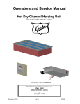
1
Data Device Corporation
NHi-156XX Terminals
NHi-157XX Terminals
Terminal + (NHi-158XX Terminals)
Bus Controller, Remote Terminal, Bus Monitor
PCI Bus And Local Bus Host Interface
User's Manual Rev. 12
Version 2010.09.13
September 2010
The information provided in this document is believed to be accurate; however, no responsibility is assumed by NATIONAL HYBRID, INC.
for its use, and no license or rights are granted by implication or otherwise in connection therewith. Specifications are subject to change
without notice.
105 Wilbur Place, Bohemia, NY 11716
1-800-DDC-5757 | 631-567-5600
[email protected] | www.ddc-web.com
-
- 1
1.0.0
SCOPE........................................................................................................................................ 7
2.0.0
NHI-156XX PROTOCOL COMPLIANCE ................................................................................... 7
3.0.0
INTRODUCTION......................................................................................................................... 7
3.1.0
3.1.1
3.1.2
3.1.3
3.1.4
FEATURES ................................................................................................................................................7
GENERAL FEATURES..........................................................................................................................7
Bus Controller Highlights ........................................................................................................................8
Remote Terminal Highlights....................................................................................................................9
Bus Monitor Highlights ...........................................................................................................................9
3.2.0
BLOCK DIAGRAMS..............................................................................................................................10
3.3.0
3.3.1
3.3.2
3.3.3
3.3.4
3.3.5
3.3.6
3.4.0
PROTOCOL CHIP DESCRIPTION .....................................................................................................11
HOST BUS INTERFACE UNIT...........................................................................................................11
MEMORY MANAGEMENT INTERFACE UNIT ..............................................................................12
INTERRUPT CONTROL UNIT ...........................................................................................................12
DUAL REDUNDANT FRONT END ...................................................................................................13
MESSAGE PROCESSOR UNIT ..........................................................................................................14
PCI INTERFACE UNIT........................................................................................................................14
RT HARDWIRE TERMINAL ADDRESS ..........................................................................................14
4.0.0
DATA STRUCTURE ................................................................................................................. 15
4.1.1
ADDRESS MAP ...................................................................................................................................15
4.1.2 INTERNAL REGISTER MAP.....................................................................................................................16
4.2.0
INTERNAL REGISTERS ......................................................................................................................17
4.2.1
CONTROL
Address: 0
R/ W BC/ MT/ RT......................................17
4.2.2 MESSAGE POINTER TABLE ADDRESS
Address: 1
R/ W
RT...........................18
4.2.3
BASIC STATUS
Address: 2
R/ W
RT .............................................18
4.2.4
INTERRUPT REQUEST
Address: 3(Ubyte)
W
BC/ MT/ RT ........................19
4.2.5
INTERRUPT MASK
Address: 3 Lbyte
R/ W BC/ MT/ RT .......................19
4.2.6
INTERRUPT VECTOR
Address: 3(Ubyte)
R
BC/ MT/ RT .......................20
4.2.7
CONFIGURATION REGISTER 2
Address: 4(Ubyte)
W
BC/ MT/ RT ......................20
4.2.8
AUXILIARY VECTOR REGISTER
Address: 4(Ubyte)
R
BC/ MT/ RT .......................21
4.2.9
REAL- TIME CLOCK ..........................................................................................................................21
4.2.10
RTC CONTROL REGISTER
Address: 7
R/ W BC/ MT/ RT ............................22
4.2.11
FIFO READ
Address: 8
R
BC/ MT/ RT .......................................23
4.2.12
FIFO RESET
Address: 8
W
BC/ MT/ RT.......................................23
4.2.13
CONFIGURATION REGISTER 1
Address: 9
R/ W BC/ MT/ RT..........................23
4.2.14
BC FRAME INDEX
Address: 10
R
BC .........................25
4.2.15
LAST COMMAND REGISTER
Address: 11
R
RT....................................................25
4.2.16
LAST STATUS REGISTER
Address: 12
R
RT........................................................25
4.2.17
MAJOR FRAME "A" ADDRESS
Address: 13
R/ W BC ..............................................25
4.2.18
ASYNCHRONOUS MINOR FRAME ADDRESS
Address: 14
R/ W BC.......................25
4.2.19
RESET REMOTE TERMINAL
Address: 15
W
BC/ MT/ RT .......................................25
4.2.20
MAJOR FRAME "B" ADDRESS
Address: 16
R/ W
BC ............................................25
4.2.21
RESERVED
Address: 17...............................................................................25
4.2.22
ENCODER STATUS
Address: 18
R
BC/ RT..................................................25
4.2.23
CONDITION REGISTER
Address: 19
R
BC/ MT/ RT .......................................26
-
- 2
4.2.24
4.2.25
4.2.26
4.2.27
4.2.28
4.2.29
4.2.30
4.2.31
4.2.32
4.2.33
4.2.34
4.2.35
4.2.36
4.2.37
4.2.38
4.2.39
4.2.40
4.2.41
4.2.42
5.0
MINOR FRAME_ TIME
Address: 20
R/ W
BC ......................................27
CONFIGURATION REGISTER 3
Address: 21
R/ W BC/ MT/RT.............................28
MT ADDRESS FILTER (15:0)
Address: 22
R/ W MT...................................29
ENCODER DATA REGISTER
Address: 23
R/W
RT ..........................................29
ENCODER DATA TRANSMIT RQST Address: 24
W
RT .........................................29
ENCODER COMMAND TRANSMIT REQUEST
Address: 25
W
RT .........................29
MT ADDRESS FILTER (31:16)
Address: 26
R/ W MT................................30
BLOCK "A" LAST ADDRESS
Address: 27
R
MT ................................30
CURRENT MINOR FRAME ADDRESS
Address: 27
R
BC.........................30
REGISTER 27 CLEAR
Address: 27
W
BC/MT...........................30
BLOCK "B" LAST ADDRESS
Address: 28
R
MT.................................30
CURRENT MESSAGE ADDRESS
Address: 28
R
BC ..............................30
REGISTER 28 CLEAR
Address: 28
W
BC/MT ...............................30
LOG POINTER TABLE ADDRESS
Address: 29
R/W RT ................................30
EXTERNAL TERMINAL ADDRESS REGISTER
Address: 30 R
BC/MT/RT....................31
BC/MT INTERRUPT VECTOR
Address: 31
R/ W BC/MT..............................31
READ- MODIFY- WRITE LOCAL BUS TERMINALS ONLY ...........................................32
BUS CONTROLLER FIFO DATA............................................................................................32
BUS MONITOR FIFO DATA ...................................................................................................32
PCI CONFIGURATION SPACE REGISTERS
PCI BUS TERMINALS ONLY ............................ 33
5.1.0
PCI CONFIGURATION SPACE REGISTER MAP ...............................................................................33
5.1.1
PCI BASE ADDRESS...........................................................................................................................33
5.1.2
PCI ADDRESSING AND DATA ........................................................................................................34
5.1.3
PCI MEMORY ADDRESSING TABLE FOR NHi-156XX TERMINALS .........................................34
5.2.0 PCI COMMANDS .........................................................................................................................................34
5.2.1 PCI COMMAND TABLE ...........................................................................................................................34
6.0.0
MEMORY MANAGEMENT ARCHITECTURE .............................................................................. 35
6.1.0
REMOTE TERMINAL MEMORY MANAGEMENT........................................................................35
6.1.1
REMOTE TERMINAL MEMORY ORGANIZATION ................................................................35
6.1.2
MESSAGE POINTER TABLE INDEX................................................................................................36
6.1.3
MESSAGE POINTER WORD..............................................................................................................36
6.1.4
SUBADDRESS POINTER TABLE CONTROL WORD .................................................................36
6.1.5
SUBADDRESS POINTER TABLE POINTERS .............................................................................37
6.1.6
DATA TABLE POINTER WORD.....................................................................................................37
6.1.7.0
REMOTE TERMINAL DATA BUFFERING SCHEME ..................................................................37
6.1.8
REMOTE TERMINAL DATA TABLE ORGANIZATION ..............................................................39
6.1.9
REMOTE TERMINAL DATA TABLE TAG WORD .........................................................................39
6.1.10
SAMPLE REMOTE TERMINAL MEMORY MAP ...........................................................................40
6.2.0
6.2.1
6.2.2
6.2.3
6.2.4
6.2.5
6.2.6
REMOTE TERMINAL MESSAGE LOG FORMAT...........................................................................45
LOG POINTER TABLE INDEX ..........................................................................................................45
SUBADDRESS LOG TABLE CONTROL WORD...............................................................................45
SUBADDRESS LOG TABLE INDEX WORD .....................................................................................46
COMMAND WORD.................................................................................................................................46
REMOTE TERMINAL LOG TABLE OPERATION............................................................................46
SAMPLE REMOTE TERMINAL MESSAGE LOG .............................................................................47
6.3.0
6.3.1
6.3.2
BUS CONTROLLER MEMORY ORGANIZATION ..........................................................................50
MAJOR FRAME ......................................................................................................................................53
MINOR FRAME .....................................................................................................................................53
-
- 3
6.3.3
6.3.4
6.3.5
6.3.6
6.3.7
6.3.8
6.3.9
MESSAGE ADDRESS TABLE................................................................................................................54
BC MESSAGE ..........................................................................................................................................54
BUS CONTROLLER DATA TABLE .......................................................................................................58
ASYNCHRONOUS FRAME......................................................................................................................59
BCU MAJOR FRAME TRIGGER.............................................................................................................59
BUS CONTROLLER APPLICATIONS ...............................................................................................59
SAMPLE BUS CONTROLLER MEMORY MAP .................................................................................60
6.4.0
MESSAGE MONITOR DATA BLOCKS .................................................................................................63
6.4.1
MESSAGE MONITOR MESSAGE BLOCKS .........................................................................................64
MESSAGE MONITOR MESSAGE BLOCK STRUCTURE........................................................................ 64
6.4.2
SAMPLE MESSAGE MONITOR MEMORY MAP .............................................................................67
6.5.0
WORD MONITOR DATA BLOCKS........................................................................................................68
6.5.1
WORD MONITOR WORD BLOCKS......................................................................................................69
6.5.2
SAMPLE WORD MONITOR MEMORY MAP ....................................................................................70
7.0
SIMULTANEOUS MONITOR AND REMOTE TERMINAL ......................................................... 71
7.1
SIMULTANEOUS MODE INTERRUPT HANDLING .........................................................................71
8.0.0
REMOTE TERMINAL MODE CODE OPERATION ................................................................ 72
8.1.0
GENERAL ...............................................................................................................................................72
8.2.0
8.2.1
8.2.2
8.2.3
8.2.4
8.2.5
8.2.6
8.2.7
8.2.8
8.2.9
8.2.10
8.2.11
8.2.12
8.2.13
8.2.14
8.2.15
8.2.16
8.2.17
8.2.18
TABLE OF RT MODE CODE RESPONSES.......................................................................................72
DYNAMIC BUS CONTROL (00000; T/ R= 1)....................................................................................72
SYNCHRONIZE WITHOUT DATA (00001; T/ R= 1)........................................................................73
TRANSMIT LAST STATUS WORD (00010; T/ R= 1).......................................................................73
INITIATE SELF TEST (00011; T/ R= 1) .............................................................................................73
TRANSMITTER SHUTDOWN (00100; T/ R= 1)................................................................................74
OVERRIDE TRANSMITTER SHUTDOWN (00101; T/ R= 1)...........................................................74
INHIBIT TERMINAL FLAG (00110; T/ R= 1)....................................................................................74
OVERRIDE INHIBIT TERMINAL FLAG (00111; T/ R= 1) ..............................................................75
RESET REMOTE TERMINAL (01000; T/ R= 1) ................................................................................75
RESERVED MODE CODES (01001- 01111; T/ R= 1).......................................................................75
TRANSMIT VECTOR WORD (10000; T/ R= 1)................................................................................76
SYNCHRONIZE WITH DATA WORD (10001; T/ R= 0)..................................................................76
TRANSMIT LAST COMMAND (10010; T/ R= 1).............................................................................77
TRANSMIT BIT WORD (10011; T/ R= 1) .........................................................................................77
SELECTED TRANSMITTER SHUTDOWN (10100; T/ R= 0)..........................................................78
OVERRIDE SELECTED TRANSMITTER SHUTDOWN (10101; T/ R= 0).....................................78
RESERVED MODE CODES (10110- 11111; T/ R= 1).......................................................................79
RESERVED MODE CODES (10110- 11111; T/ R= 0).......................................................................79
9.0
INITIALIZATION .......................................................................................................................... 79
9.1
INTERNAL INITIALIZATION ...............................................................................................................79
9.2
HOST INITIALIZATION OF TERMINAL............................................................................................80
10.0
INTERRUPT HANDLING .......................................................................................................... 81
-
- 4
10.1
HARDWARE ACKNOWLEDGE
10.2
SOFTWARE ACKNOWLEDGE...........................................................................................................82
11.0
PC BOARD CONSIDERATIONS AND GUIDE LINES ............................................................. 82
12.0
PIN FUNCTIONAL DESCRIPTION ........................................................................................... 83
12.0
PIN FUNCTIONAL DESCRIPTION ........................................................................................... 83
12.1
GENERAL PURPOSE SIGNALS...........................................................................................................83
12.2.0
LOCAL BUS TERMINALS ONLY ........................................82
HOST INTERFACE SIGNALS – LOCAL BUS TERMINALS .......................................................83
12.3
HOST INTERFACE SIGNALS – PCI BUS TERMINALS............................................................84
12.4
DISCRETE I/O SIGNALS.......................................................................................................................84
12.5
MIL-BUS INTERFACE SIGNALS .....................................................................................................85
12.6
POWER SIGNALS................................................................................................................................85
13.0
ELECTRICAL CHARACTERISTICS.......................................................................................... 86
13.1
ABSOLUTE MAXIMUM RATINGS ......................................................................................................86
13.3
I/O TYPES & DESCRIPTIONS...............................................................................................................86
13.4
I/O ELECTRICAL CHARACTERISTICS.............................................................................................87
14.0.0
14.0.1
14.0.2
14.0.3
14.0.4
14.0.5
14.0.6
14.0.7
TIMING DIAGRAMS – LOCAL BUS TERMINALS................................................................. 88
HOST WRITE CYCLE – LOCAL BUS TERMINALS.......................................................................88
HOST READ CYCLE – LOCAL BUS TERMINALS ........................................................................88
HOST READ- MODIFY- WRITE CYCLE – LOCAL BUS TERMINALS........................................89
HARDWARE INTERRUPT ACKNOWLEDGE CYCLE – LOCAL BUS TERMINALS ......................89
TERMINAL ADDRESS READ CYCLE................................................................................................90
SOFTWARE INTERRUPT ACKNOWKEDGE - LOCAL BUS TERMUNALS ..................................90
TIMING NOTES – LOCAL BUS TERMINALS ................................................................................91
14.1.0
14.1.1
14.1.2
14.1.3
TIMING PARAMETER TABLES FOR LOCAL BUS TERMINALS .............................................91
HOST READ, WRITE, READ- MODIFY- WRITE TABLE and .......................................................91
TERMINAL ADDRESS READ TABLE – LOCAL AND PCI BUS TERMINALS...........................91
HARDWARE INTERRUPT ACKNOWLEDGE CYCLE TABLE....................................................92
15.0
PIN FUNCTION TABLE ............................................................................................................. 93
15.1 UNIVERSAL PIN FUNCTIONS 68 PIN QUAD FLAT PACK LOCAL BUS TERMINALS .............93
15.2 UNIVERSAL PIN FUNCTIONS
68 PIN QUAD FLAT PACK
PCI BUS TERMINALS...................94
15.3 UNIVERSAL PIN FUNCTIONS PLASTIC BGA PACKAGE LOCAL BUS TERMINALS ..............95
-
- 5
15.4 UNIVERSAL PIN FUNCTIONS PLASTIC BGA PACKAGE PCI BUS TERMINALS .....................96
15.5 TERMINAL+ UNIVERSAL PIN FUNCTIONS
15.6
GENERIC PACKAGE OUTLINE DRAWINGS
PBGA PACKAGE
97
100
15.7
BALL GRID ARRAY PACKAGE..............................................................................................................101
17.0
ORDERING INFORMATION .................................................................................................... 104
18.0
REVISIONS............................................................................................................................... 107
19.0
APPLICATION NOTES ........................................................................................................... 109
19.1
LOOP BACK TEST OPERATION ..........................................................................................................109
19.2
MODIFIED LOOPBACK TEST ...........................................................................................................110
19.3.0
SOFTWARE INTERFACE ...................................................................................................................112
19.3.1
GENERAL............................................................................................................................................112
19.3.2
PCI BUS "C" CODE FRAGMENT......................................................................................................112
19.3.4 LOCAL BUS "C" CODE FRAGMENT.................................................................................................113
-
- 6
1.0.0
SCOPE
This document defines the functional and electrical specification for National Hybrid's series
of MIL- STD- Data Bus Expanded Capabilities terminals(NHi-156XX).
2.0.0
NHi-156XX PROTOCOL COMPLIANCE
MIL- STD- 1553A
MIL- STD- 1553B Notices I and II
MIL- STD- 1760B
MCAIR MDC A3818, A5690, A4905, A5332
EFA/ STANAG- 3838 requirements for Eurofighter Aircraft
3.0.0
INTRODUCTION
The NHi- 156XX is a low cost complete Multi-Protocol Mil- Std- Data Bus Interface between a dual
redundant bus and a host processor. The device functions as a programmable Bus Controller, Remote
Terminal, Bus Monitor and simultaneous Monitor/Remote Terminal. It contains a protocol chip, two
monolithic transceivers and 64K word SRAM. The unit is available packaged in a .95" x .95" 69 pin
ceramic PGA, or .95" x .95" 68 pin ceramic quad flatpack. The only external components required are two
coupling transformers.
The NHi-156XX appears to the host computer as 64K words of 16 bit wide memory controlled by
standard RAM signals. The device can thus be easily interfaced with all popular processors and buses.
The built in interrupt controller supports an internal FIFO which retains header information for queuing up
to 6 pending interrupt requests plus an overflow interrupt.
All modes of operation access data tables via pointers residing in RAM which facilitates multiple buffering.
This allows buffers to change without moving data and promotes efficient use of RAM space. The data
tables have programmable sizes and locations.
The NHi-156XX defaults to remote terminal operation on power up.
3.1.0
FEATURES
3.1.1
GENERAL FEATURES
•Multi-Protocol Interface
•PCI bus or Local Bus interface to host processor.
•Operates from 20 Mhz clock.
•+5V monolithic transceivers
•+3.3v logic.
•Appears to host as a Dual Port Double Buffered 64K x 16 SRAM
•Footprint less than 1 square inch
•Ensures integrity of all shared data and control structures
•Built- in interrupt controller
•Internal FIFO is configurable to retain header information for queuing up to 6 pending interrupt
requests plus an overflow interrupt, or as a 7 interrupt revolving FIFO
•Provides interrupt priority input and output pins for daisy- chaining interrupt requests
•Contains a Timer Unit which provides 32 bit RTC (Real- Time- Clock) with 1, 2, 4, 8, 16, 32 and
64 uS internal, or user provided external clock resolution for data and event time tagging.
•Selectable 768/ 672 us Failsafe Timer with complete Testability.
•Double buffering of messages and data tables.
•Low power CMOS technology
-
- 7
3.1.2
Bus Controller Highlights
•Implements all Message Formats and Error Checking
•Major and minor frame message structure.
•Simple setup and operation. Multiple minor frames, message tables and data tables. Only one
Major Frame Pointer Register is required to control unlimited number of messages
•BC initialized by writing to three Configuration Registers and the Interrupt Mask Register
•Executes lists of messages via Minor Frame Pointers
•Configurable Local Retry and Interrupt Requests Enabled on Message by Message Basis
•Configurable Global Retry and Message Specific Local Retry
•Programmable retries per message:
None
Retry Current Bus
Retry Alternate Bus
Retry Alternate Bus then Current Bus.
•Programmable response timeout of 14, 18, 26, or 42 microseconds.
•Programmable Intermessage Gap Time up to 4 mS with 2uS resolution.
•Programmable Synchronous Message Time up to 4mS with 2uS resolution.
•Extended Gap Time and Synchronous Message Time using NO- OP Feature.
•Programmable Minor Frame Gap with 64 us resolution.
•Programmable Interrupts for:
End of Message
End of Frame
Response Time Out, Message
Error
Message Retry
RT Status Bit Set
FIFO Overflow.
•Host controlled commands:
Start BC
Continuous Mode
Stop at End of Message
Stop at End of Frame
Abort,
GOTO Alternate Frame.
•Dynamic Message Bus Switch Upon Successful Retry.
•Synchronous or Asynchronous Messages.
•Synchronous or Asynchronous Minor Frames.
•Up to 63 autonomous data tables per message.
-
- 8
3.1.3
Remote Terminal Highlights
•Dynamic Bus Control Acceptance
•DBCA_ L bit is set in configuration register.
•Message Illegality is internally programmable. DOES NOT require external PROMS or glue
logic.
•Employs data tables with individual tag words which indicate data validity, data latency,
table status and broadcast
•Optionally sets the subsystem flag bit whenever stale data is transmitted or received data is
overwritten.
•Issues interrupts on any subset of T/ R bit, subaddresses, mode commands, broadcast
messages and errors.
•Optionally resets the real- time clock in response to a "Synchronize" mode command.
•Optionally updates the lower 16 bits of the real- time clock in response to a "Synchronize
With Data" command.
•Indicates the reception of specific commands by outputting pulse on discrete pin.
•Internally loops- back messages under host control for test purposes.
•Employs a decoder algorithm which ensures high noise immunity and a low error rate.
•Software RT Address Lockout.
•MDC3818 Status Response, Error Handling, Status Bit Definition, Mode Code Operation.
•Separate Broadcast Interrupts.
•Up to 63 autonomous data tables per message.
•Multiple and individual message logs provide expedited message analysis.
3.1.4
Bus Monitor Highlights
•Simple setup and operation
•Preset multiple data blocks.
•Only one MT Data Start Address Register is required to control
unlimited number of message blocks. The data block sizes and locations are totally
Programmable.
•MT initialized by writing to three MT Configuration Registers and the MT Interrupt Mask Register.
•Error detection and reporting
•All encoding, timing and protocol errors defined by the Protocols are detected.
•Programmable Monitor Modes:
Word Monitor, transfers all data with/ without ID and Time Tag words.
- Message Monitor, transfers all Command and Status words with/ without ID and Time Tag ,
while data words are transferred directly to conserve memory space.
•Concurrent Bus Monitor and Remote Terminal operation.
•Selective Message Monitor, based on RT Address.
•Programmable Interrupt for End of Block.
-
- 9
3.2.0
BLOCK DIAGRAMS
LOCAL BUS TERMINAL BLOCK DIAGRAM
HADR(16:1)
PROTCOL
BUS_A
HCS_L;HRD_L;HWR_L
BC
T/R_A
BUS_A_L
HDAT(15:0)
BCUTGR_L
RT
BCUFRMEND_PLS_H
INTPI_L
TXA_ENA_L
MT
INTACK_L
DTACK_L
MT/RT
BUS_B
INTPO_L_DSC_H
PLSCMD_H
MCD01_PLS_H
T/R_B
BUS_B_L
SSF_TF_L
TXB_ENA_L
MCD08_PLS_H
IRQ_L
CONTROL
CMDS_H
SRAM
DATA
EXT_TMG_H
LCLK_H
MRST_L
RTADR(4:0); PAR
PCI BUS TERMINAL BLOCK DIAGRAM
PROTCOL
BUS_A
BUS_A_L
BC
T/R_A
CBE((3:0)
AD(31:0)
PARBIT_H
STOP_L
RT
DEVSEL_L
TRDY_L
TXA_ENA_L
MT
MT/RT
BUS_B
IRDY_L
FRM_L
IDSEL_H
PCICLK_H
PLSCMD_H
SSF_TF_/BCUTGR_L
L
MCD08_PLS_H
T/R_B
BUS_B_L
TXB_ENA_L
IRQ_L
CONTROL
CMDS_H
SRAM
DATA
EXT_TMG_H
LCLK_H
MRST_L
RTADR(4:0); PAR
-
- 10
The NHi-156XX contains two monolithic transceivers, an ASIC, and an SRAM. The ASIC performs all
multi protocol functions; BUS CONTROLLER, BUS MONITOR and REMOTE TERMINAL. It controls
accesses to the RAM such that it appears to the host CPU 16bit wide dual port memory.
Since the NHi-156XX appears to its host as RAM, no external logic is required when interfacing to local
bus terminal. It is simply connected to the CPU's address bus, Mil Bus, and control lines. There are NO
EPROMS required to illegalize commands in the RT mode. Illegalization is performed internal to the
protocol chip. The user sets up command illegalization when the NHi-156XX is initialized. See sections on
Message Illegalization and Host Initialization.
Local bus terminals can be interfaced to an 8 bit CPU Bus by folding the upper and lower bytes on top of
each other and performing byte wide data transfers.
By default, the host has priority in accessing the I/ O bus. When a local bus host requests access to a
device already in use by the protocol chip, the host *DTACK signal is delayed by the NHi-156XX. If either
side (protocol chip or host) waits for access during the current cycle, it is automatically granted priority for
the next cycle. The host can retain priority for successive cycles accessing the same address (this is
required to guarantee the proper operation of host read- modify- write instructions - see pin *HCS for
details) by keeping *HCS low.
Notice that the 5 bit hardwire address and address parity bit used for Remote terminal operation are
connected to the Sram data bus. This is done to reduce pin count. Because of this arrangement, the
hardwire address and parity pins MUST NOT be connected directly to ground or +3.3v, doing so will
corrupt the Sram data bus. Use 4.7k pull-down resistors to set a logic "0" on the terminal address lines
and the parity bit. Use 4.7K or 10K pull-ups to ups to +3.3v for a logic "1".
The Hardwire Address pins must NOT be left floating. If the Hardwire Address is not used, all 5
bits plus the Address Parity bit must have pull-ups to +3.3v.
Another alternative is to connect a tri-state address buffer to the terminal address and parity lines. It will
automatically be enabled by CMDS_H when the hardwire address is read.
3.3.0
PROTOCOL CHIP DESCRIPTION
The protocol chip contains the following modules:
Host Bus Interface Unit
Memory Management Interface Unit
Interrupt Controller Unit
Dual Redundant multi protocol Front End
Message Processor Unit
PCI Interface Unit
(HBIU)
(MMIU)
(ICU)
(DRFE)
(MPU)
(PCIIU)
3.3.1
HOST BUS INTERFACE UNIT
The HBIU provides a standard RAM or PCI interface to the host bus. The module performs the following
functions:
Provides device select and decodes host address to select registers.
Transfers data between the NHi-156XX and the host (word, byte and read-modify- write
are supported in local bus terminals).
Provides priority input and output for daisy chaining host interrupts.
Outputs *DTACK signal indicating end of bus cycle.
Provides PCI interface for PCI terminals.
-
- 11
3.3.2
MEMORY MANAGEMENT INTERFACE UNIT
The MMIU controls the RAM bus so that it appears to the host as a pseudo dual port RAM (i. e., shared
memory). The unit implements the following functions:
Arbitrates between host and protocol chip initiated accesses to the RAM and host data
Decodes address lines to select device (e. g. RAM, external terminal address buffer,
internal register).
Generates control signals to access the selected device.
bus.
3.3.3
INTERRUPT CONTROL UNIT
The ICU is an 8 input vectored interrupt controller. It contains eight registers as well as a FIFO for storing
pending interrupt vectors.
3.3.3.1
ICU REGISTERS
The ICU contains the following registers
INTERRUPT REQUEST register
INTERRUPT MASK register
INTERRUPT VECTOR register
AUXILIARY VECTOR register
(IRR)
(IMR)
(IVR)
(AVR)
The INTERRUPT REQUEST register samples 8 inputs originating from internal modules. Since the host
can write to this register, all interrupt sequences can be software driven for program debugging. The
inputs and their priorities (level 7 has highest priority) are described in the following table.
3.3.3.1.1
INTERRUPT DEFINITION TABLE
PRIORITY/MASK
0
1
2
3
4
5
6
7
RTU
GOOD MESSSAGE
BAD MESSAGE
GOOD MODE CODE
BAD MODE CODE
FIFO FULL
GOOD BROADCAST
BAD BROADCAST
FAILSAFE TIMEOUT
BCU
MESSAGE END
FRAME END
MESSAGE ERROR
RETRY
FIFO FULL
STATUS SET
NO RESPONSE
FAILSAFE TIMEOUT
MTU
N/A
N/A
N/A
N/A
FIFO FULL
BLOCK END
N/A
N/A
Note: RT Interrupts 5 & 6 are enabled only when separate Broadcast Tables are used.
Masking interrupt 4 creates a revolving Fifo.
As soon as an interrupt is requested, its vector is pushed onto the FIFO - so the chronological order of the
requests normally determines the order in which they will be serviced. Simultaneous requests, however,
are pushed onto the FIFO according to the priority of the pending interrupts.
The INTERRUPT MASK register masks the corresponding inputs to the INTERRUPT REQUEST register.
The INTERRUPT VECTOR register holds the 3 bit interrupt priority level and an additional 5 bit field (see
paragraph on INTERRUPT VECTOR register for details).
The AUXILIARY VECTOR register contains an additional byte of information related to the interrupt
request (see paragraph on AUXILIARY VECTOR register for details).
-
- 12
3.3.3.2
ICU FIFO
The ICU FIFO is 16 bits wide and 7 words deep. Whenever an unmasked interrupt request is issued by
the message processor, a word is pushed onto the FIFO. When an interrupt is acknowledged by the host,
a word is popped from the FIFO and used to update the IVR and the AVR.
The host can read the FIFO by simply popping its contents. This is done by reading the FIFO located at
address 8 (refer to address map). The interrupt request output, *IRQ, will go inactive after the FIFO is
emptied in this way.
The host can mask the *IRQ output by resetting the INTERRUPT REQUEST ENABLE bit in the
CONTROL register; however this does not prevent the device from pushing interrupt requests onto the
FIFO.
If an interrupt request occurs when the FIFO is full, a vector indicating FIFO overflow is first pushed onto
the FIFO and then the vector which caused the overflow is pushed onto the FIFO. As a result, the 2
oldest vectors are lost. All further pushes are then inhibited until the host pops the vector indicating the
overflow.
The above mechanism ensures that the host will always be notified of FIFO overflows and will always
obtain the 2 interrupt vectors immediately preceding the overflow condition.
If interrupt 4 is masked, the FIFO operates in the revolving mode; vectors are continuously pushed onto
the FIFO. After the 7th vector is pushed without any pops, each additional vector pushed causes the
oldest vector to be lost.
The FIFO can be emptied by writing (any value) to address 8 (in words).
3.3.4
DUAL REDUNDANT FRONT END
The DRFE performs serial to parallel and parallel to serial conversion as well as basic format and timing
validation. The unit contains the following:
Manchester encoders/ decoders
Gap counter
No response counter
Minimum response time counter
Timeout counter
3.3.4.1
MANCHESTER DECODER
The decoder translates serial Manchester bi- phase signals to 16- bit words and outputs the following
signals:
Valid command word received
Valid data word received
Invalid word received (parity, incorrect bit count, invalid Manchester encoding, gap)
Broadcast command received
Begin new message (i. e., end of a valid legal command for this Remote Terminal)
3.3.4.2
MANCHESTER ENCODER
The encoder receives 16 bit words and transmits them with the appropriate sync and parity as a serial
Manchester bi- phase signal. The outputs of the encoder can be loop- backed into either decoder for test
purposes.
-
- 13
3.3.4.3
GAP COUNTER
The gap counter checks contiguity of successive words. If the time between "contiguous" words
(measured from zero- cross of parity to zero- cross of sync) exceeds 3.5 - 3.7 microseconds, the
message is invalidated.
3.3.4.4
RT - RT NO RESPONSE COUNTER
The no response counter checks the response time of the transmitting RT in a RT to RT transfer. If the
response time is exceeded, the message is invalidated. The response time is software programmable
(14, 18, 26, 42 microseconds) to accommodate systems with long cables and/ or slow terminals.
3.3.4.5
MINIMUM RESPONSE TIME COUNTER
The minimum response time counter ensures that the response will be no sooner than 4 microseconds
(measured from zero- cross of parity to zero- cross of sync).
3.3.4.6
FAIL -SAFE TIMEOUT COUNTER
This counter inhibits the encoder outputs and issues a TIMEOUT interrupt whenever continuous
transmission exceeds 768/ 672 microseconds. Transmission will remain inhibited until a command is
received on the same bus or the part is reset.
3.3.5
MESSAGE PROCESSOR UNIT
The MPU forms the heart of the protocol chip and controls the operation of the Decoders, Encoders, and
Interrupt Controller. This unit is activated by the reception of a valid legal command addressed to the RT
in the RT mode and the START bit in CONFIGURATION 1 in both the BC and MT modes.The MPU
performs the following functions:
Recognizes the various message types (for BC, MT, and RT) and responds with the
appropriate sequence of control signals.
Validates format and timing of received data words.
Checks command legality.
Responds with status/ data.
Calculates all addresses for accessing the RAM and discrete I/ O.
Updates RAM data table contents, including tag words.
Optionally time tags data tables.
Issues interrupt requests to the ICU.
The maximum response time of the NHi-156XX in the RT mode is less than 5.0
microseconds (measured from zero- cross to zero- cross).
3.3.6
PCI INTERFACE UNIT
The PCIIU is an internal PCI bridge that is used in the PCI bus terminals to connect directly to a
PCI slot without the need for and external bridge. The PCIIU contains the PCI configuration
registers and an internal bridge which transfer data between the PCI bus and the 1553 terminal.
3.4.0
RT HARDWIRE TERMINAL ADDRESS
The terminal address of the NHi-156XX can be hardwired using RTADR( 5: 0). RTADR( 4: 0) are used for
the terminal address, RTADR0 being the LSB, and RTADR5 is used to set odd parity in the address.
These pins CANNOT be directly connected to +3.3v or ground since they are the data Bus for the internal
RAM. The hardwire terminal address and the parity pin must be set using pull- up and pull- down
resistors. 4.7K or 10K pull-up resistors for a logic "1" and 4.7k pull-down resistors for a logic "0". The
Hardwire Address is read and loaded into the terminal at Power- On Reset, Hardware Reset, and
Software Reset.
The Hardwire Address pins must NOT be left floating. If the Hardwire Address is not used, all 5
bits plus the Address Parity bit must have pull-ups to +3.3v.
The terminal address can be changed at any time through software by writing a new address to the Basic
Status Register, however, if any of the above resets occur, the Hardwire Address will be re- loaded into
the terminal. The software address can be locked out by setting Bit2 in Configuration Register 1.
-
- 14
4.0.0
DATA STRUCTURE
4.1.1
ADDRESS MAP
The NHi-156XX appears to the host as 64K words of memory divided into the following blocks:
ADDRESS RANGE(dec)
0 -- 31
32 --63
64 -- 65535
-
DESCRIPTION
INTERNAL REGISTERS
RESERVED
SHARED RAM
- 15
4.1.2 INTERNAL REGISTER MAP
ADDR
ESS
0
1
2
3
3
3
4
4
4
5
6
7
8
8
9
10
11
12
13
14
15
16
17
18
19
20
21
22
23
24
25
26
27
27
27
28
28
28
29
30
30
31
REGISTER DEFINITION
ACCESS
CONTROL
RT MESSAGE POINTER TABLE ADDRESS
BASIC STATUS
INTERRUPT MASK(lower byte)
INTERRUPT VECTOR(upper byte)
INTERRUPT REQUEST(upper byte)
INTERRUPT VECTOR(lower byte)
AUXILLARY VECTOR(upper byte)
CONFIGURATION 2(upper byte, BCU/MTU only)
REAL TIME CLOCK HIGH WORD
REAL TIME CLOCK LOW WORD
REAL TIME CLOCK CONTROL
READ FIFO
RESET FIFO
CONFIGURATION 1
BCU CURRENT MAJOR & MINOR FRAME INDEX
LAST COMMAND
LAST STATUS
BCU-MAJOR FRAME “A” ADDRESS; MTU-BLOCK "A" ADDRESS
ASYNCHRONOUS FRAME ADDRESS
RESET TERMINAL(both bytes)
BCU-MAJOR FRAME “B” ADDRESS; MTU-BLOCK "B" ADDRESS
RESERVED
ENCODER STATUS
CONDITION
BCU FRAME GAP/WORD MTU END OF FRAME OPTIONS
CONFIGURATION 3
MESSAGE MONITOR ADDRESS FILTER(0 -- 15)
ENCODER DATA*
ENCODER DATA TX REQUEST*
ENCODER COMMAND TX REQUEST*
MESSAGE MONITOR ADDRESS FILTER(16 -- 31)
MONITOR BLOCK “A” LAST ADDRESS
BCU CURRENT MINOR FRAME ADDRESS
CLEAR REGISTER 27
MONITOR BLOCK “B” LAST ADDRESS
BC CURRENT MESSAGE ADDRESS
CLEAR REGISTER 28
RT LOG POINTER TABLE ADDRESS
EXTERNAL RTU ADDRESS BUFFER(lower byte)
RESERVED
BC & MT INTERRUPT VECTOR
R/W
R/W
R/W
R/W
R
W
R/W
R
W
R
R
R/W
R
W
R/W
R
R
R
R/W
R/W
W
R/W
R/W
R
R
R/W
R/W
R/W
R/W
W
W
R/W
R
R
W
R
R
W
R
W
R/W
*In order to write to addresses 23, 24, or 25, the terminal must be in loop- back in the RT mode
(see CONTROL register for details).
-
- 16
4.2.0
INTERNAL REGISTERS
4.2.1
CONTROL
Address: 0
This register controls the general operation of the terminal.
15
14
13
12
11
FRMTM
RSP1
RSP0
TSTFST
NBCST
7
6
5
4
3
IRE
INHBJM
MSGTM SRQRST SSF_TF
FRMTM
1 = BC minor frames are synchronous.
A minor frame has a defined periodic time.
R/ W
BC/ MT/ RT
10
TXINH
2
LOGENA
Bits: 15
9
LOOPB
1
BINH
8
LOOPA
0
AINH
BC/
0 = BC minor frames are asynchronous.
Minor frame time is dependent on the number of messages, message time,
Frame gap and RT response time.
RSP1, RSP0
Bits: 14,13
BC/ RT
These bits define the response timeout for RT- RT messages in the RT mode and terminal response
timeout in the BC mode as follows:
RSP1
RSP0
TIMEOUT(us)
0
0
56
0
1
60
1
0
68
1
1
84
TSTFST
Bits: 12
RT
1= Enables testing of the FAIL SAFE time out.
When this feature is enabled, the RT will transmit continuously once it is enabled by a valid
message. The encoder will be inhibited after 768/ 672us. It will be enabled by a reset or the
reception of another valid message. If this bit is set to 0 during an RT transmission, before
the required number of words have been transmitted, the encoder will return to normal
operation and stop at the proper message length.. If it is set to 0 after the message length
has been exceeded, the current word will be completed and normal operation resumed.
This feature can be used in the LOOP BACK mode to automatically transmit data words.
The RT encoder will remain in the tester mode until the CPU sets this bit to 0.
The TSTFST Bit Must Always Be Set to Zero During Normal Operation!!!
NBCST
Bits: 11
1= Specifies that broadcast commands WILL be ignored by the RT.
RT
TXINH
Bits: 10
BC/ RT
1= Inhibits transmission by forcing TXA= TXAN= 0 and TXB= TXBN= 0.
LOOPA( B)
Bits: 9, 8
RT
1= Defines that decoder A (B) inputs shall be connected internally to the encoder outputs rather
than the transceiver for test purposes.
IRE
Bits: 7
BC/ MT/ RT
1= Globally enables the interrupt request output, *IRQ.
0= Disables all interrupt requests; however, interrupt vectors are still pushed onto the FIFO.
-
- 17
INHBJM
1 = Inhibits BC bus jam function.
Bits: 6
BC
0 = Bus jam enabled. BC will accept and discard up to 31 extra words from an RT before
aborting the message. A message error will be declared even when extra words are
accepted and discarded.
MSGTM
1 = BC messages are synchronous.
A message has a defined periodic time.
Bits: 5
BC
0 = BC messages are asynchronous.
Message time is dependent on the message gap and the response time of the RT.
SRQRST
Bits: 4
RT
1= Specifies that the service request bit in the STATUS word will be reset upon reception of a
valid "Transmit Vector Word" mode command.
SSF_ TF
Bits: 3
RT
0= Specifies that the Sub- System Flag in the Status Word will be determined by the value
of the SSF_ TF pin.
1= Specifies that the Terminal Flag in the Status Word will be determined by the value of the
SSF_ TF pin.
LOGENA
Bits: 2
RT
1= Enables message logging of RT messages. Segregated message logs can be
created for individual message types(i.e. Log1: receive subaddress 1; Log2: transmit
subaddress 5). Integrated message logs can be created for multiple
message types(i.e. Log3: transmit subaddress 8,10,20, receive subaddress,3,7,9).
BINH
1= Disables reception on bus B.
Bits: 1
BC/ RT
AINH
1= Disables reception on bus A.
Bits: 0
BC/ RT
4.2.2 MESSAGE POINTER TABLE ADDRESS
Address: 1
R/ W
RT
This register contains the address of the table of pointers used in the RT mode. The address is specified
as a word address . After POR, the register is initialized to 1000 (hex).
4.2.3
BASIC STATUS
Address: 2
R/ W
RT
This register defines the terminal address as well as default values for all status bits. The Status Word is
OR'ed with this register before transmission. The bits in the BASIC STATUS register correspond to the
bits in the STATUS register and their function is defined in MIL- STD- 1553B.
They can be redefined for other protocols.
15
TADR4
7
RSVD2
14
TADR3
6
RSVD1
13
TADR2
5
RSVD0
12
TADR1
4
BCR
-
- 18
11
TADR0
3
BUSY
10
M_ERR
2
SSF
9
INSTR
1
DBCA
8
SREQ
0
TF
The mechanism employed by the protocol chip for initializing the terminal address is designed to avoid
dedicated pins(see block diagram). Upon POR the terminal address and its parity are automatically read
from address 30. The value can be supplied in 2 ways: by enabling the output of an external terminal
address buffer or by employing pull- up/ down resistors to define a default terminal address. Odd parity is
used to define a valid terminal address; even parity will inhibit reception on both buses. After POR, the
host can change the terminal address through software by writing to the TADR field with any desired
value. In addition, this operation will enable reception. Providing Bit 2 of Configuration Register is set to
“0”.
The host can check the validity of the parity bit obtained from the terminal address by reading address 30;
if the most significant bit in the lower byte equals 1, the parity is invalid.
If the TADR is not defined externally (by pull- down resistors or a buffer), there is no danger of a false
response before host initialization because internal pull- up resistors on the terminal address guarantee
an incorrect terminal address parity.
When BUSY= 1, 1553 message accesses to the RAM are inhibited, however the RT will respond with
status as required by MIL- STD- 1553B. The mode commands "Transmit Status Word", "Transmit Last
Command Word", "Reset Remote Terminal", "Transmitter Shutdown", "Override Transmitter Shutdown"
and the reserved mode commands legalized by MIO (see the CONTROL register for details) are not
affected by BUSY. In addition, all output pulses issued after valid command reception are inhibited when
BUSY= 1 (except for the signal MDCDRST which is pulsed after receiving the mode command "Reset").
After POR( MRST), BUSY is set to "1"; this prevents the RT from using undefined pointers before the host
has had a chance to initialize the POINTER TABLE. The default value for all other status bits is "0" and
the TADR field is loaded with the hardwired address.
The BUSY Bit in the LAST STATUS REGISTER is cleared on receipt of the first command after a
RESET, except if that command is TRANSMIT LAST STATUS or TRANSMIT LAST COMMAND
mode command.
The BUSY Bit in the LAST STATUS REGISTER can be cleared by bit using
CONTROL REGISTER. See RTC CONTROL REGISTER for details.
BIT 5 in the RTC
4.2.4
INTERRUPT REQUEST
Address: 3(Ubyte)
W
BC/ MT/ RT
The INTERRUPT REQUEST register holds 8 types of interrupt requests (see section on INTERRUPT
CONTROL UNIT for details). Interrupt requests are active high and upon POR the register is cleared (see
initialization section).
15
IRQ7
14
IRQ6
13
IRQ5
12
IRQ4
11
IRQ3
10
IRQ2
9
IRQ1
8
IRQ0
4.2.5
INTERRUPT MASK
Address: 3 Lbyte
R/ W BC/ MT/ RT
The INTERRUPT MASK register masks the corresponding interrupts. Upon POR, all interrupts are
masked (see initialization section).
7
IMSK7
6
IMSK6
5
IMSK5
4
IMSK4
1= Interrupt is masked.
0= Interrupt is enabled.
-
- 19
3
IMSK3
2
IMSK2
1
IMSK1
0
IMSK0
4.2.6
INTERRUPT VECTOR
Address: 3(Ubyte)
R
BC/ MT/ RT
INTERRUPT VECTOR
Address: 4(Lbyte )
R/ W BC/ MT/ RT
The IVR is read only in the upper byte at address 3 and is read/ write in the lower byte at address 4. It
contains interrupt header information which is popped off the FIFO.
ADDR3(4)
RT
(BC/MT)
15(7)
14(6)
13(5)
12(4)
11(3)
9(2)
10(1)
8(0)
D4
A7
D3
A6
D2
A5
D1
A4
D0
A3
L2
A2
L1
A1
L0
A0
The Interrupt Vector register is loaded from the fifo when it is popped. The FIFO is popped by a
hardware interrupt acknowledge or a read to address 8. This register in undefined at POR.
L(2: 0)
RT
This is the interrupt priority determined by the message processor which is defined in the Interrupt
Definition Table.
D(4: 0)
RT
The DDDDD field is inputted by the CPU. This is used as an offset for the interrupt vector. During a
hardware interrupt acknowledge, this register is outputted on the upper and lower bytes of the CPU data
bus.
A(7: 0)
BC/MT
In the BC and MT modes, the A field is the lower eight bits of the address of the message or the frame
which caused the interrupt. See sections 4.2.41 and 4.2.42.
4.2.7
CONFIGURATION REGISTER 2
Address: 4(Ubyte)
This register is used for operational control of the part.
15
14
13
12
11
10
GO DEF
FRAME
ABORT
STOP AT
EOF
STOP AT
EOM
CLR
DISC
RSVD
W
BC/ MT/ RT
9
8
RSVD
RSVD
GO_ DEF_ FRAME
Bits: 15
BC/ MT
When a "1" is written to this bit, the DEFAULT FRAME, defined by bit 12 in CONFIGURATION
REGISTER 1, is made the active frame.
ABORT
Bits: 14
BC/ MT
When a "1" is written to this bit, all BC and MT processing is terminated and the NHi-156XX goes offline. The BC or the MT must be re- started to again become active.
STOP END OF FRAME
Bits: 13
BC/ MT
When a "1" is written to this bit, the BC or the MT will go off- line after the last message in the frame or
block has been processed. The BC or the MT must be re- started to again become active.
STOP END OF MESSAGE
Bits: 12
BC/ MT
When a "1" is written to this bit, the BC or the MT will go off- line after the current message in the frame
or block has been processed. The BC or the MT must be re- started to again become active.
CLR DISC FLAG
Bits: 11
RT
When a "1" is written to this bit, the 1760 DISCONNECT FLAG is cleared. This flag indicates that a store
has been released and all the address bits and the parity bit on the hardwire address are "1's". The flag is
read on the IPO_ DSC pin and bit 6 of the EXTERNAL TERMINAL ADDRESS REGISTER.
-
- 20
4.2.8
AUXILIARY VECTOR REGISTER
Address: 4(Ubyte)
R
BC/ MT/ RT
This register contains additional information related to the interrupt request. The data is popped from the
FIFO and latched into the AVR during the interrupt acknowledge cycle or whenever the FIFO is popped
by a host read instruction to address 8. Upon POR, this register is undefined.
MODE
15
14
13
12
11
9
10
8
RTU
EMP
BUS
T/R
BCU/MTU
A15
A14
A13
SADR4
MODE4
A12
SADR3
MODE3
A11
SADR2
MODE2
A10
SADR1
MODE1
A9
SADR0
MODE0
A8
EMP
1= Fifo empty. Ignore data.
0= Fifo data valid. Use data.
Bits: 15
RT
BUS
Bits: 14
0= Indicates that the message was on bus A
1= Indicates that the message was on bus B.
RT
T/ R
0= Indicates a receive message.
1= Indicates a transmit message.
RT
Bits: 13
SADR / MODE
Bits: (12-8)
RT
This field defines the sub- address or mode code.
Note: the interrupt level distinguishes between regular transmit/ receive commands and mode
commands.
A(15 : 8)
Bits: (15-8)
BC/MT
In the BC and MT modes, the A field is the upper eight bits of the address of the message or the frame
which caused the interrupt. See sections 4.2.41 and 4.2.42.
4.2.9
REAL- TIME CLOCK
RTC HIGH WORD
Address: 5
R
BC/MT/RT
RTC LOW WORD
Address: 6
R
BC/MT/RT
The RTC is a 32 bit up- counter which can be used for time- tagging in the BC, MT and RT modes. If the
time- tagging option is in effect, the RTC is sampled and stored in 2 words in the data table The most
significant word is stored first.
When messages are time- tagged in the RT mode, the host should not write data to the first 2 locations
following the data table tag word since they will be overwritten with the value of the message time tag.
In the RT mode, the RTC can be reset by the mode command "Synchronize Without Data" and the least
significant 16 bits can be updated by "Synchronize With Data". The full 32 bits can be updated using the
first two data words in a receive command. See RTC CONTROL REGISTER for details.
The RTC can be read and reset by the host at any time. Since the RTC consists of 32 bits, at least 2
memory cycles are required to read all of its value. As a result, a carry- out from the lower word can
occur between the read cycles. A mechanism is therefore provided to solve this potential difficulty.
-
- 21
If the host reads the RTC as two 16 bit words, *LOCK should be initialized to 1 in the RTC CONTROL
register. In this case, when the host reads the upper word, all 32 bits are latched into the host output
register. The value in the output register remains unchanged until the host finishes reading the lower word
of the RTC.
If the host reads the RTC in bytes, *LOCK should be initialized to 0. In this case, when the host reads any
of the bytes of the RTC, all 32 bits are latched into the host output register and its value remains
unchanged until updating is re- enabled by reading the RTC CONTROL register. The RTC resolution can
be programmed equal to 1, 2, 4, 8, 16, 32, or 64 microseconds.
4.2.10
RTC CONTROL REGISTER
Address: 7
R/ W BC/ MT/ RT
The RTC CONTROL register controls the RTC as well as having other functions.
15
14
13
12
11
10
9
8
RTC
RESET
RESET
LAST
RES2
SYNUPD
*LOCK
SYNRST
RES1
RES0
7
M1760
6
BUSY
OPT
5
RESET
BUSY
4
PRESET
4
3
PRESET
3
2
PRESET
2
1
PRESET
1
0
PRESET
0
RTC RESET
Bits: 15
BC/ MT/ RT
When a "1" is written to RTC RESET, a reset pulse is issued to the RTC. The contents of the register
are not affected by this operation and RTC RESET is always read by the host as "0".
RESET LAST
Bits: 14
BC/ MT/ RT
When a "1" is written to RESET LAST, all the bits in the LAST STATUS REGISTER except the
ADDRESS field and the BUSY bit are set to a "0". The contents of the register are not affected by this
operation and RESET LAST is always read by the host as "0".
SYNUPD
Bits: 12
RT
1= Specifies that the lower 16 bits of the RTC will be updated whenever a valid mode command
"Synchronize With Data" is received by the ET.
*LOCK
Bits: 11
BC/ MT/ RT
0 = Enables updating of the host output register after the RTC CONTROL register is read (this
feature is needed to support byte wide read cycles).
1 = Enables updating of the host output register after the lower RTC word is read.
SYNRST
Bits: 10
RT
1= Specifies that the RTC shall be reset whenever a valid mode command "Synchronize Without
Data" is received by the terminal.
RES
Bits: 13, 9, 8
BC/ MT/ RT
This field defines the resolution of the RTC in microseconds as follows:
RESOLUTION(us)
13
9
8
1
0
0
0
2
0
0
1
4
0
1
0
8
0
1
1
16
1
0
0
32
1
0
1
64
1
1
0
EXT
1
1
1
-
- 22
M1760
Bits: 7
RT
1= Specifies that the RT shall comply with MIL- STD- 1760A. This mode of operation has two
consequences: first, the mode command "Synchronize With Data" updates the lower 16 bits
of the RTC only if the least significant data bit is "0" and second, the IPO_ DSC pin serves as
a store disconnect signal rather than an interrupt priority output.
0= Specifies that the RT shall comply with MIL-STD-1553B.
BUSY _OPT
Bits: 6
RT
0= MRST, Software Reset and MODE CODE_ 08 RESET will set the BUSY bit in the LAST
STATUS REGISTER and the BASIC STATUS REGISTER to a "1".
1= Only MRST will set the BUSY bit in the LAST STATUS REGISTER and the BASIC STATUS
REGISTER to a "1".
RESET BUSY
Bits: 5
RT
When a "1" is written to RESET BUSY, the BUSY bit in the LAST STATUS REGISTER is set to a "0".
The contents of the register are not affected by this operation and RESET BUSY is always read by the
host as "0".
PRESET
Bits: (4: 0)
RT
These bits provide a method to perform a double word( 32 bit) preset to the RTC. When this bit field is
set to any number from 1 to 30( bit 0 = LSB), the first two words of a receive message whose subaddress
is equal to this value will be used to preset the internal RTC. The most significant word is received first. If
this field is equal to a "0" or "31", the RTC will not be preset. All bits in this register are cleared during
initialization.
4.2.11
FIFO READ
Address: 8
R
BC/ MT/ RT
This address is used to read the contents of the interrupt FIFO. Reading this address pops the FIFO,
updates the IVR and the AVR; then outputs the AVR(upper byte) and IVR(lower byte) as a 16 bit word.
For BCU and MTU operation, if the AVR and the IVR both contain zero after a FIFO pop(0000h), this
indicates that the FIFO is EMPTY.
For RTU operation, if the AVR contains 80h and the IVR contains 00h after a FIFO pop(8000h), this
indicates that the FIFO is EMPTY.
4.2.12
FIFO RESET
Address: 8
Writing any value to this address empties the FIFO.
W
BC/ MT/ RT
4.2.13
CONFIGURATION REGISTER 1
Address: 9
This register is used to configure the functionality of the part.
15
MONITOR
TYPE
14
13
GLOBAL
BUS_SEL1
GLOBAL
BUS_SEL0
7
0
6
0
5
INHIBIT
DBCA
12
11
FRAME
BLOCK
4
GLOBAL
DBS
R/ W
10
BC/ MT/ RT
9
3818
MODE
FUNCTION
SELECT1
FUNCTION
SELECT0
3
LOCAL
2
INHIBIT
1
CONVERT
0
SEP BCST
DBS
SOFTADR
BUSY BIT
TABLES
Note: Reserved Bits 7- 6 must be set to "0".
MONITOR TYPE
0 = Word Monitor.
1 = Message Monitor .
Bits: 15
-
8
START
BCU_MTU
- 23
MT
GLOBAL BUS_ SEL
Bits: 14, 13
BC
These bits determine the Bus select options.
GLOBAL BUS
COMMENTS
14
DEFAULT
USE BC CONTROL WORD BUS
0
FORCE BUS “A”
FORCE ALL MESSAGES TO BUS “A”
0
FORCE BUS “B”
FORCE ALL MESSAGES TO BUS “B”
1
FORCE ALT BUS USE OPPOSITE BUS OF BC CONTROL WORD
1
FRAME/ BLOCK
0 = Default Frame /Block is "A".
1 = Default Frame/Block is "B".
Bits: 12
BC/ MT
START_ BC_ MT
1 = Start Bus Controller or Monitor.
Bits: 11
BC/ MT
13
0
1
0
1
3818_ STATUS
Bits: 10
RT
0 = Status response and protocol operation as defined in Mil- Std- 1553B.
1 = Status response and protocol operation as defined in MDC A3818 and Mil- Std- 1553A.
FUNCTION SELECT
Bits: 9, 8
BC/ MT/ RT
OPERATIONAL MODE
9
8
REMOTE TERMINAL
0
0
BUS CONTROLLER
0
1
MONITOR
1
0
MONITOR & REMOTE TERMINAL
1
1
Note: In the Monitor/RT mode, the broadcast address is ignored by the RT.
INHIBIT DBCA
Bits: 5
RT
0 = DBCA bit in Status Word is set upon receipt of a valid DBCA Mode Code.
1 = Prevents DBCA Bit in Status Word from being set upon receipt of a valid DBCA Mode Code.
GLOBAL_ DYNAMIC_ BUS_ SELECTION
Bits: 4
BC
0 = Message bus unchanged after successful Global Retry.
1 = Automatically switch message to alternate bus in BC Control Word after successful retry on
alternate bus due to a Global Retry option.
LOCAL_ DYNAMIC_ BUS_ SELECTION
Bits: 3
BC
0 = Message bus unchanged after successful Local Retry.
1 = Automatically switch message to alternate bus in BC Control Word after successful retry on
alternate bus due to Local Retry option.
INHIBIT SOFT_ ADR
Bits: 2
RT
0 = Bits (15: 11) of Basic Status Register set the RT Address when a Write Operation to that
register is performed. The Hard Wired Address sets the RT Address at RESET.
1 = Prevents software change of RT Address when writing to the Basic Status Register.
Bits (15: 11) of Basic Status Register are “Don’t Care”. Only the Hard Wired Address sets the
RT Address at RESET.
CONVERT BUSY BIT
Bits: 1
RT
0 = BUSY Bit is compliant with Mil- Std- 1553B.
1 = Converts BUSY Bit to Non- 1553B operation. BUSY Bit becomes a standard bit with no
special functionality. BUSY Bit is not set during software reset or MODE CODE_ 08 RESET.
-
- 24
SEP_ BCST_ TABLES
Bits: 0
RT
0 = Broadcast messages use the same pointers as receive message:. therefore, receive and
broadcast messages are stored in the same data tables. The BCST bit in the tag word is
used to differentiate between the two message types.
1 = An additional 30 pointers are activated which puts receive and broadcast messages in
separate data tables.
4.2.14
BC FRAME INDEX
Address: 10
Bits(15:8) contain the index offset into the current major frame.
Bits(7:0) contain the index offset into the current minor frame.
R
BC
4.2.15
LAST COMMAND REGISTER
Address: 11
R
RT
This register holds the last command word as defined by the MIL-BUS. The contents are not defined after
initialization of the RT.
4.2.16
LAST STATUS REGISTER
Address: 12
R
RT
This register holds the Status Word associated with the last message. After initialization of the RT, the
BUSY bit= 1, the TADR field contains the hardwire address, and all other bits are set to 0. See RTC
CONTROL REGISTER for special options.
4.2.17
MAJOR FRAME "A" ADDRESS
Address: 13
R/ W BC
BLOCK "A" START ADDRESS
R/W
MT
This register contains the 16 bit address of BC Major frame “A” or MT data block “A”.
4.2.18
ASYNCHRONOUS MINOR FRAME ADDRESS
Address: 14
R/ W BC.
This register contains the 16 bit address of the BC Minor asynchronous frame . The asynchronous Minor
frame will execute at the end of the current BC message if bit 15 of
configuration register 3(address21) is a ‘1’.
4.2.19
RESET REMOTE TERMINAL
Address: 15
W
BC/ MT/ RT
Writing a word to address 15 resets the RT and causes it to perform its initialization (see initialization
section).
4.2.20
MAJOR FRAME "B" ADDRESS
Address: 16
R/ W
BC
BLOCK "B" START ADDRESS
R/W
MT
This register contains the 16 bit address of BC Major frame “B” or MT data block “B”.
This register contains the 16 bit FRAME "B" POINTER. This is the address of the active message list to
be used by the BC or the MESSAGE MONITOR for FRAME "B".
In the WORD MONITOR, this register contains the 16 bit start address of BLOCK "B".
4.2.21
RESERVED
Address: 17
4.2.22
ENCODER STATUS
Address: 18
R
BC/ RT
This register contains flags indicating the status of the encoder. These flags are intended to facilitate
transmission of messages in loop- back mode during self- test.
15
TXREQ_L
7
EOTX_L
0
FAILSAFE_L
TXREQ_ L
Bits: 15
RT
0= Indicates that the encoder is ready to accept the next word for transmission. This bit should
equal "0" before loading the Encoder Data register with the next word. In order to transmit
contiguous words, the next word should be loaded within 18 microseconds after *TXREQ
transitions to "0".
-
- 25
EOTX_ L
Bits: 7
RT
0= Indicates that the encoder has completed transmission and that there are no pending
requests.
FAILSAFE_ L
Bits: 0
BC/ RT
0= FAILSAFE TIME OUT has occurred. This bit will be set to a "1" when a new message is
received or during a reset.
4.2.23
CONDITION REGISTER
Address: 19
R
BC/ MT/ RT
This register contains information about the command being processed and the operational condition of
the terminal.
15
ASYNC
FRAME
14
X
13
12
11
10
9
AXEN
BXEN
TFE
X
MDCD_L
8
X
7
6
5
4
3
2
1
0
X
CUFRM
BUSY
EOF B
EOF A
CUR
FRM
CUR
BUS
BUSJAM
B
BUSJAM
A
ASYNC FRAME
1 = Asynchronous frame is currently running.
Bits 15
BC
0 = Asynchronous frame NOT currently running.
AXEN
Bits: 13
BC/ RT
1= Indicates that transmitter A is enabled. This bit is set to a "1": at POWER UP, if the terminal is
RESET, after receipt of a "Reset" mode code, or after receipt of an OVERRIDE
TRANSMITTER SHUTDOWN mode code on the B bus.
0= Indicates that transmitter A is inhibited. This bit is set to a "0" after receipt of TRANSMITTER
SHUTDOWN mode code on the B bus.
BXEN
Bits: 12
BC/ RT
1= Indicates that transmitter B is enabled. This bit is set to a "1": at POWER UP, if the terminal is
RESET, after receipt of a "Reset" mode code, or after receipt of an OVERRIDE
TRANSMITTER SHUTDOWN mode code on the A bus.
0= Indicates that transmitter B is inhibited. This bit is set to a "0" after receipt of a
TRANSMITTER SHUTDOWN mode code on the A bus.
TFE
Bits: 11
RT
1= Indicates that the TERMINAL FLAG bit in the status word can be set to a "1" . This can be
done in the BASIC STATUS REGISTER or by the TERMINAL FLAG pin. This
bit is set to a "1" at POWER UP, if the terminal is RESET, after receipt of a RESET MODE
CODE, or after receipt of an OVERRIDE INHIBIT TERMINAL FLAG mode code.
0= Indicates that the TERMINAL FLAG bit in the status word CANNOT be set to a "1". This bit is
set to a "0" after receipt of an INHIBIT TERMINAL FLAG mode code.
MDCD_ L
Bits: 9
1= Indicates that the last command received was NOT a mode code.
0= This bit is set to a "0" when a mode code is received.
CUFRM BUSY
1= The current frame of data block is busy.
data.
RT
Bits: 6
BC/ MT
It is active and could be receiving or transmitting
EOF B
Bits: 5
BC/ MT
1= Frame "B" or data block "B" has finished processing data and in now inactive.
-
- 26
EOF A
Bits: 4
BC/ MT
1= Frame "A" or data block "A" has finished processing data and in now inactive.
CUR FRM
Bits: 3
0= Frame "A" or block "A" is the current active frame of block.
1= Frame "B" or block "B" is the current active frame of block.
BC/ MT
CUR_ BUS
0= Bus "A" is the current bus.
1= Bus "B". is the current bus.
BC/ MT
Bits: 2
BUSJAM B
Bits: 1
BC
1 = Bus "B" has been jammed by continuous transmission from an RT. This condition is
indicated when an RT transmits more extra words then the value set in CONFIGURATION
REGISTER 3 (See CONFIG REG 3 for details).
BUSJAM A
Bits: 0
BC
1 = Bus "A" has been jammed by continuous transmission from an RT. This condition is
indicated when an RT transmits more extra words then the value set in CONFIGURATION
REGISTER 3 (See CONFIG REG 3 for details).
4.2.24
MINOR FRAME_ TIME
Address: 20
R/ W
BC
MONITOR_ EOF_ OPTIONS
M/T
BC OPERATION: For synchronous frames, this 16 bit register specifies the absolute time duration of a
minor frame. When the frames are asynchronous, this 16 bit register specifies the minor frame END_
OF_ FRAME_ DELAY before starting the next minor frame. The time resolution is 100 us.
MT OPERATION: This register specifies the END- OF- MESSAGE block options.
MONITOR
15
0
7
END OF B
INT
14
0
6
RSVD
13
0
5
12
0
4
11
0
3
BLOCK B
END OPT1
BLOCK B
END OPT0
END OF A
INT
10
0
2
RSVD
9
0
1
8
0
0
BLOCK A
END OPT1
BLOCK A
END OPT0
Note: Bits 15- 8 are reserved in the monitor mode and should be set to “0”.
END OF B INT
Bits: 7
MT
1 = The Word Monitor will cause an interrupt when End of Block "B" is reached.
0 = End of Block WILL NOT cause an interrupt.
BLOCK B END_ OPT
Bits: 5, 4
MT
These two bits determine a course of action at the end of BLOCK "B" in the Word Monitor.
BLOCK B END OPTIONS
5
4
STOP AT END OF BLOCK B
0
0
REPEAT BLOCK B
0
1
GOTO BLOCK A
1
0
STOP AT END OF BLOCK B
1
1
ENDOF A INT
Bits: 3
MT
1 = The Word Monitor will cause an interrupt when End of Block "A" is reached.
0 = End of Block WILL NOT cause an interrupt.
-
- 27
BLOCK A END_ OPT
Bits: 1, 0
MT
These two bits determine a course of action at the end of BLOCK "A" in the Word Monitor.
BLOCK A END OPTIONS
STOP AT END OF BLOCK A
REPEAT BLOCK A
GOTO BLOCK B
STOP AT END OF BLOCK A
1
0
0
1
1
0
0
1
0
1
4.2.25
CONFIGURATION REGISTER 3
Address: 21
R/ W
This register is used to set global parameters for the BC and the MT.
BC/ MT/RT
15
14
13
12
11
10
9
8
ASYNC
FRAME
WORD MT
NTTGDAT
WORD MT
NTAG
WORD MT
NTTAG
MSG MT
NTAG
MSG MT
NTTAG
GLOBAL
RETRY1
GLOBAL
RETRY0
7
6
5
4
3
2
1
0
STAT SET
RETRY
ADR LAT
INHIBIT
RSVD
BUSJAM4
BUSJAM
3
BUSJAM
2
BUSJAM
1
BUSJAM
0
BC ASYNCHRONOUS FRAME QUEUE
Bits: 15
BC
1 = The BC asynchronous Minor frame, whose address is located in register 14, is queued to run
and will execute at the end of the message in the current minor frame.
Bit 15 will be cleared automatically by the protocol chip.
0 = The BC asynchronous frame is NOT queued to run..
WORD MT NTTGDAT
Bits: 14
MT
0 = A 32 bit time tag is stored with data words and command/ status words.
1 = No time tag on data words. Only command/Status words are time tagged.
WORD MT NTAG
Bits: 13
0 = A Tag word is stored with Data and Command/Status words.
1 = No tag word.
MT
WORD MT NTTAG
Bits: 12
MT
0 = Word Monitor time tag is enabled. Bit 14 determines the time tag format.
1 = No time tagging. Word Monitor time tag is disabled.
MSG MT NTAG
Bits: 11
0 = Tag word is stored with Command/Status words.
1 = No tag word.
MT
MSG_ MT NTTAG
Bits: 10
MT
0 = Message Monitor time tag is enabled. Command/Status words are time tagged.
1 = Message Monitor time tag is disabled.
GLOBAL RETRY
Bits: 9, 8
BC
These bits define a global default retry scenario. If the BC control word defines no retry as the option for a
message, then the global retry is enabled. If the global retry is defined as no retry, then their will not be a
retry for the message.
GLOBAL RETRY OPTIONS
9
8
NO RETRY
0
0
RETRY ACTIVE BUS
0
1
RETRY ALTERNATE BUS
1
0
RETRY ALTERNATE BUS, THEN ACTIVE BUS
1
1
-
- 28
STAT SET RETRY
Bits: 7
BC
This bit determines if a retry will be executed when a status word invokes a status set condition.
0 = No retry on status set.
1 = Retry if a status bit is set.
ADR LAT INHIBIT
Bits: 6
RT
This bit determines whether or not the CPU address will be automatically latched by the HCS_ L.
0 = CPU address is automatically latched within 200ns after the falling edge of HCS_ L.
1 = CPU address is manually stored in a transparent when ADR_ LAT_ L input signal is a “1”.
Note:: This option is not available on all parts.
RESERVED
Bits: 5
BUS JAM
Bits: 4: 0
BC
These bits determine the number of excess words that will be accepted from an RT without declaring that
the bus has been jammed by an RT that is transmitting continuously. The range is from 0 to 31 words.
The msb is bit 4. All the excess words received are discarded.
If a BUS_ JAM is detected, the BC declares an error, aborts the message and moves on to the next
message in the minor frame.
If the number of excess words received is insufficient to detect a BUS_ JAM, the BC declares an error,
aborts the message and moves on to the next message in the minor frame.
4.2.26
MT ADDRESS FILTER (15:0)
Address: 22
R/ W MT
This register determines which RT addresses, from 0 to 15 will be monitored in the MESSAGE MONITOR
mode.
0 = Accept RT address, store data.
1 = Ignore RT address, NO data stored.
15
14
13
12
11
10
9
8
MASK 15
MASK 14
MASK 13
MASK 12
MASK 11
MASK 10
MASK 09
MASK 08
7
6
5
4
3
2
1
0
MASK 07
MASK 06
MASK 05
MASK 04
MASK 03
MASK 02
MASK 01
MASK 00
NOTE: When the terminal is operating in the concurrent Monitor-Remote Terminal mode,
the Remote Terminal address MUST NOT be filtered out in the Monitor.
4.2.27
ENCODER DATA REGISTER
Address: 23
R/W
RT
This register contains data to be transmitted when performing a loop back test.
4.2.28
ENCODER DATA TRANSMIT RQST Address: 24
W
RT
Writing (any value) to this address causes the contents of the ENCODER DATA REGISTER to be sent as
a data word. This instruction together with the ENCODER COMMAND TRANSMIT REQUEST can be
used to loop- back entire messages for self- test purposes. The received data can be read from the data
table associated with the command.
4.2.29
ENCODER COMMAND TRANSMIT REQUEST
Address: 25
W
RT
Writing (any value) to this address causes the contents of the ENCODER DATA REGISTER to be sent as
a command word. This instruction is useful for sending commands to the decoder while in loop- back
mode. The command can then be read from the LAST COMMAND register.
-
- 29
4.2.30
MT ADDRESS FILTER (31:16)
Address: 26
R/ W MT
This register determines which RT addresses, from 16 to 31 will be monitored in the MESSAGE
MONITOR mode.
0 = Accept RT address, store data.
1 = Ignore RT address, NO data stored.
15
14
13
12
11
10
9
8
MASK 31
MASK 30
MASK 29
MASK 28
MASK 27
MASK 26
MASK 25
MASK 24
7
6
5
4
3
2
1
0
MASK 23
MASK 22
MASK 21
MASK 20
MASK 19
MASK 18
MASK 17
MASK 16
NOTE: When the terminal is operating in the concurrent Monitor-Remote Terminal mode,
the Remote Terminal address MUST NOT be filtered out in the Monitor.
4.2.31
BLOCK "A" LAST ADDRESS
Address: 27
R
MT
This register contains the 16 bit address of the last word in monitor BLOCK "A". The last address is
calculated by the protocol chip. It is not necessarily equal to the BLOCK "A" end address specified in
the first word in data block “A”.. In order to keep all the words together, they are stored contiguously and
the last ACTUAL address in BLOCK "A" is stored in this register; therefore, addresses must always be
reserved after the specified end address to accommodate this situation. This register is continually
updated with the address of each word as it written into the ram.
4.2.32
4.2.33
CURRENT MINOR FRAME ADDRESS
Address: 27
This register contains the address of the current MINOR frame.
R
REGISTER 27 CLEAR
Address: 27
Writing any value to this address clears register 27.
W
BC
BC/MT
4.2.34
BLOCK "B" LAST ADDRESS
Address: 28
R
MT
This register contains the 16 bit address of the last word in monitor BLOCK "B". The last address is
calculated by the protocol chip. It is not necessarily equal to the BLOCK "B" end address specified in
the first word in data block “B”.. In order to keep all the words together, they are stored contiguously and
the last ACTUAL address in BLOCK "B" is stored in this register; therefore, addresses must always be
reserved after the specified end address to accommodate this situation. This register is continually
updated with the address of each word as it written into the ram.
4.2.35
CURRENT MESSAGE ADDRESS
Address: 28
This register contains the address of the current BC message.
4.2.36
REGISTER 28 CLEAR
Address: 28
Writing any value to this address clears register 28.
R
W
BC
BC/MT
4.2.37
LOG POINTER TABLE ADDRESS
Address: 29
R/W RT
This register contains the 16 bit address RT Log Pointer Table. If bit 2 in register 0 is a ‘1’, the RT
will log all messages received or a subset of the received messages..
-
- 30
4.2.38
EXTERNAL TERMINAL ADDRESS REGISTER
Address: 30
This register contains information about the hardwire terminal address.
15
14
13
12
11
10
RSVD
RSVD
RSVD
RSVD
RSVD
RSVD
R
BC/MT/RT
9
8
RSVD
RSVD
7
6
5
4
3
2
1
0
INVALP
DISCON
TADRP
TADR4
TADR3
TADR2
TADR1
TADR0
Note: The hardwire address lines must NOT be left floating.
The terminal address may be hardwired using external resistors on the RT address and parity pins. Pullups of 4.7K or 10K and pull-downs of 4.7K should be used.. Address parity is wired for odd parity in the
address. The hardwire terminal address and its parity can be obtained by reading I/ O address 30.
This address is unique since a read operation activates the CMDS_H strobe As a result, a buffer
containing the terminal address can be read without decoding address lines. If an external buffer is not
desired, pull- up/ down resistors on the I/ O data bus can be used instead (see BASIC STATUS register
for details). The protocol chip also calculates the terminal address's parity and compares it to the value
obtained from the I/ O bus.
INTPND……………………………….Bits: 12
1 = The FIFO contains one or more interrupts.
INVALP
Bits: 7
1= Specifies that the terminal address which was read automatically by the protocol chip
following reset (from I/ O address 30) had invalid parity.
DISCON
Bits: 6
0= Specifies that the store is disconnected because a terminal address of 31 was detected on
the I/ O bus for at least 800 nanoseconds.
1= Specifies that the store is connected.
This bit indicates the "disconnected store" condition defined by MIL- STD- 1760A, provided that the store
contains the pull- down resistors used for defining the terminal address (see BASIC STATUS register for
details). After the store is disconnected, the standby state of all I/ O lines will be high and will therefore
define an illegal terminal address of 31.
TADRP
Bits: 5
TADRP equals the value of the terminal address parity read from I/ O address 30.
TADR
Bits: (4:0)
TADR equals the value of the terminal address read from I/ O address 30.
4.2.39
BC/MT INTERRUPT VECTOR
Address: 31
R/ W BC/MT
The IVR is read only in the upper byte at address 3 and is read/ write in the lower byte at address 4. It
contains interrupt header information which is popped off the FIFO.
BIT
15
14
13
12
11
9
10
8
MT
D4
D3
D2
D1
D0
L2
L1
L0
BIT
7
6
5
4
3
2
1
0
BC
D4
D3
D2
D1
D0
L2
L1
L0
The Interrupt Priority bits are loaded from the FIFO when it is popped. The FIFO is popped by a
hardware interrupt acknowledge or a read to address 8. This register in undefined at POR.
-
- 31
L(2: 0)
This is the interrupt priority determined by the message processor which is defined in the Interrupt
Definition Table.
D(4: 0)
The DDDDD field is inputted by the CPU. This is used as an offset for the interrupt vector. During a
hardware interrupt acknowledge, this register is outputted on the upper and lower bytes of the CPU data
bus.
4.2.40
READ- MODIFY- WRITE LOCAL BUS TERMINALS ONLY
The host Read- Modify- Write cycle is used to support CPUs similar to the Motorola 680X0 where certain
instructions (eg:, test and set) require two contiguous accesses to memory. Such accesses are unique in
that the address remains active for both cycles.
4.2.41
BUS CONTROLLER FIFO DATA
Interrupt
0
1
2
3
4
5
6
7
Description
A15 - A8
A7 - A0
End-of-Message
Message Addr UB
Message Addr LB
End-of-Frame
Frame Addr UB
Frame Addr LB
Error
Message Addr UB
Message Addr LB
Retry
Message Addr UB
Message Addr LB
Fifo verflow
0
4
Status Set
Message Addr UB
Message Addr LB
No Response
Message Addr UB
Message Addr LB
Failsafe Time out
0
7
Fifo Empty
0
0
When the Fifo is popped, the Auxillary vector register is loaded with A15 - A8, while the Interrupt Vector
register is loaded with A7 - A0.
4.2.42
BUS MONITOR FIFO DATA
Interrupt
0
1
2
3
4
5
6
7
Description
A15 - A8
A7 - A0
Not Used
Not Used
Not Used
Not Used
Fifo verflow
0
4
End of Data Block
Block Addr UB
Block Addr LB
Not Used
Not Used
0
7
Fifo Empty
0
0
When the Fifo is popped, the Auxillary vector register is loaded with A15 - A8, while the Interrupt Vector
register is loaded with A7 - A0.
-
- 32
5.0
5.1.0
PCI CONFIGURATION SPACE REGISTERS
PCI BUS TERMINALS ONLY
PCI CONFIGURATION SPACE REGISTER MAP
ADDRESS(hex)
00000000
00000002
00000004
00000006
00000008
000000009
0000000A
0000000B
0000000C
0000000D
0000000E
00000010
00000014
00000018
0000001C
00000020
00000024
00000028
0000002C
0000002E
00000030
00000034
0000036
00000038
000003C
0000003D
000003E
000003F
DATA(hex)
1758
5625
0002
0400
00
00
80
07
00
00
00
FFC00000
000000000
00000000
00000000
00000000
00000000
00000000
1758
5625
00000000
0000
0000
00000000
00
01
00
00
REGISTER
Vendor Id
Device Id
Command
Status
Revision Id
Program Id
Sub Class
Base Class
Cache Line Size
Latency Timer
Header Type
Base Address
Base Address
Base Address
Base Address
Base Address
Base Address
Card Bus CIS Pointer
Subsystem Vendor Id
Subsystem Id
Expansion Rom
Capabilities Pointer
Reserved
Reserved
Interrupt Line
Interrupt Pin
Min_Gnt
Max_Lat
5.1.1
PCI BASE ADDRESS
Base address register 0x10 is used to store the PCI memory base address. If 0xFFFFFFFF
Is written to this base address register, 0xFFC00000 will be read back. This reserves 4 Mb of PCI
memory space for the terminal.
The PCI controller will assign a base address to the NHi-156XX terminal. This base address will be in the
range 0x00400000 to 0xFFC00000.
-
- 33
5.1.2
PCI ADDRESSING AND DATA
The NHi-156XX memory is organized on 16 bit word boundaries. Register are 16 bits wide and memory
is stored as 16 bit words, therefore each address increment is one 16 bit word or two bytes..
When addressing the terminal via the PCI bus, double word addressing is used, therefore each address
increment on the PCI bus is four bytes. PCI data is 32 bits wide, however only the lower 16 bits are
used to transfer data to the terminal, the upper 16 bits should be set to '1'.
The memory mapped pointer to the PCI terminal should be defined as PULONG.
The PCI memory offset is four times the desired internal memory address of the NHi-156XX.
The following table gives examples which illustrate the relationship between the PCI memory offset and
an internal address in the NHi-156XX terminal.
Only type 0 addressing is recognized by the NHi-156XX PCI terminals. Address bits 0 and 1 of the PCI
address/data bus must be set to "0" during the addressing phase of a command.
5.1.3
PCI MEMORY ADDRESSING TABLE FOR NHi-156XX TERMINALS
PCI MEMORY
OFFSET(Hex)
TERMINAL INTERNAL
MEMORY ADDRESS(Hex)
00000000
00000004
0000008
0000002C
00000074
00000400
000048D0
0002EB44
00035FA4
0003FFFC
0000
0001
0002
000B
001D
100
1234
BAD1
D7E9
FFFF
FUNCTION
Control Reg
Pointer Table Addr Reg
Basic Status Reg
Last Command Reg
Log Pointer Table Addr Reg
Terminal Ram
Terminal Ram
Terminal Ram
Terminal Ram
Terminal Ram MSW
The PCI address is given by:
(PCI Base Address) + (PCI Memory Offset).
5.2.0 PCI COMMANDS
NHi-156XX terminals use a subset of the available PCI commands, all other PCI commands are not
implemented. If the NHi-156XX receives a PCI command that is not implemented, it ignores the
command and takes no action
5.2.1
PCI COMMAND TABLE
CBE_3-0
0110
0111
1010
1011
COMMAND TYPE
MEMORY READ
MEMORY WRITE
CONFIGURATION READ
CONFIGURATION WRITE
The four PCI commands shown in this PCI Command Table are the only PCI commands implemented in
the NHI-156XX PCI terminals.
-
- 34
6.0.0 MEMORY MANAGEMENT ARCHITECTURE
The memory management operation of the Remote Terminal, Bus Controller and Monitor is summarized
in this section.
6.1.0
REMOTE TERMINAL MEMORY MANAGEMENT
The RTU memory manager used in the NHi-156XX terminals is very flexible and has the
following features:
•Double buffering of all messages.
•Up to 63 data tables per message.
•True asynchronous message handling and support.
•Autonomous message data table swap.
•Smart message data table swap
•Coherent non-fragmented message data tables.
•32 bit time tag.
•Message illegality.
The mapping scheme is illustrated in the following diagram:
6.1.1
REMOTE TERMINAL MEMORY ORGANIZATION
The T/R bit subaddress and word count fields in the Command word are used to index into a message
Pointer table as defined below:
Message Pointer
Table Address
16 Bits
Message Pointer
Table(16Bit Ptrs)
Subaddress Data Table
Pointers(16Bit Ptrs)
Pointer 0
Receive Subaddress 1
Table Control Word
Pointer 1
Pointer To Data Table 1
Up To 63 Pointers
Per Message
Pointer To Data Table 63
Pointer 127
-
- 35
6.1.2
MESSAGE POINTER TABLE INDEX
Index
T/R
Subaddress
Mode Code
0
Not Used
1 - 30
0
1 - 30
31
0
31 (Note 2)
32
Not Used
33 - 62
1
1 - 30
63
1
31 (Note 2)
64 - 95
X
0,31 (Note 2)
0 - 31
96
Not Used
97 - 126
0
1 - 30
127
0
31 (Note 2)
Note 1: Broadcast messages may be separate or combined with Receive.
Note 2: Subaddress 31 is an extended subaddress for 3818A/1553A, Not a
Command
Receive/Bcst
Receive/Bcst
Transmit
Transmit
Mode Code
Broadcast
Broadcast
Mode Code Flag
6.1.3
MESSAGE POINTER WORD
The message Pointer Word provides the 16 bit word address of the Subaddress Pointer Table for the
message:
15
ADDR16
14
13
12
11
10
9
8
ADDR15
ADDR14
ADDR13
ADDR12
ADDR11
ADDR10
ADDR09
7
6
5
4
3
2
1
0
ADDR08
ADDR07
ADDR06
ADDR05
ADDR04
ADDR03
ADDR02
ADDR01
ADDR( 16: 1)
Bits: 16:1
Set by CPU
Defines the location of the Subaddress Pointer table for the message.. These tables always begin on
word boundaries.
MESSAGE ILLEGALITY
Commands are illegalzed by setting the corresponding Message Pointer word in the Message Pointer
Table to 0. When the protocol chip receives an illegal command, it responds with ME= 1 in the status; in
addition, data transmission and storage are suppressed. All undefined mode commands are ignored.
6.1.4
Bits:(5-0)
Table Size:
SUBADDRESS POINTER TABLE CONTROL WORD
Set by CPU
Defines number of pointers to data tables in Subaddress Table.
Maximum number of pointers is 63
Bit(6)
Bit(7)
Not Used.
Message-Lock
Set by Terminal
1 = Terminal is accessing currently indexed data table.
0 = No data table in this message is being accessed by the terminal.
Bits(13-8)
Pointer INDEX:
Set by Terminal
INDEX(1-63) is offset to Pointer To last data table used
By this message.
This field identifies the Subaddress pointer used for the most recent message processed or currently
being processed.
An index of 0 indicates a virgin set of data tables.
-
- 36
Time Tag Options
All Messages Are Time Tagged(i.e. receive, transmit,
mode code).
Bits(14)
Applies to transmit messages only.
1
0
Set by CPU
Transmit Time Tag in Data Words 1 & 2.
Time Tag not transmitted with data.
Bit(15)
Index Update Options
0
Set by CPU
Only update index if message had no errors. Error
data will not be saved.
Always update index; even if message had errors.
Error data will be saved.
1
6.1.5
SUBADDRESS POINTER TABLE POINTERS
Each pointer is the address of a data table for that message. There can be up to 63 pointers per
message type; therefore each message type(receive subaddress 1 for example) can have up to 63
messages stored in different data tables without having any data overwritten. The data tables are
autonomously selected by the terminal when the same message is received multiple times. No CPU
intervention is required.
6.1.6
DATA TABLE POINTER WORD
The Data Table Pointer Word has the following format:
15
ADDR16
14
13
12
11
10
9
8
ADDR15
ADDR14
ADDR13
ADDR12
ADDR11
ADDR10
ADDR09
7
6
5
4
3
2
1
0
ADDR08
ADDR07
ADDR06
ADDR05
ADDR04
ADDR03
ADDR02
ADDR01
ADDR( 16: 1)
Bits: 16:1
Set by CPU
Defines the location of a data table associated with the message. Message data tables always begin on
word boundaries.
6.1.7.0
REMOTE TERMINAL DATA BUFFERING SCHEME
Since the host and the NHi-156XX can access data tables asynchronously, data integrity must be
ensured by a suitable buffering scheme. A brief description of data buffering is given below.
6.1.7.1
REMOTE TERMINAL DATA BUFFERING OPERATION
This technique uses a Message pointer index table which contains 128 pointers; one for each receive
subaddress, one for each transmit subaddress, one for each mode code and one for each broadcast
subaddress. Each pointer in this table is the address of a Subaddress pointer table; therefore, each
subaddress and mode code has its own Subaddress pointer table.
The subaddress pointer table contains a Table Control Word, which defines the maximum number of data
table pointers(up to 63) , each of which is the address of a data table. The Table Control Word also
contains an index indicating the offset to the most recent pointer used by the Protocol chip. . A time tag
option bit enables transmission of the 32 bit time tag in the first two data words of a transmit message. All
messages are time tagged. The first pointer is located at offset 1 into the table. An Update Option bit
permits the index to be updated only on error free messages or regardless of message errors. The
Message Lock bit indicates that the protocol chip is accessing the (index) data table.
-
- 37
Before selecting the next pointer in the Subaddress Pointer table, the protocol chip reads the Table
control word and if the pointer Index number is less than the Message Max, it selects the next pointer,
accesses the data, then updates the pointer Index number based on the setting of the Update Option bit..
If the Index is at Message Max, the first pointer is selected, its data table is reused and the pointer Index
set to 1. The overwrite bit is also set in the tag word of that data table.
There are two methods the CPU can use to retrieve data. The first is the pointer swap technique, the
second is the direct access approach.
POINTER SWAP --- RECEIVE MESSAGES
The CPU exchanges the pointer of the selected subaddress or mode code in the Message Pointer
Table with that in a subordinate table. It now has buffered access to all the pointers in that subaddress
pointer table and their associated data tables, and the protocol chip has access to a new set of pointers
and data tables for message processing.
The CPU then reads a pointer in the table, reads the tag word, checks the Lock bit, if set waits till cleared
or comes back later, gets the data, then proceeds to the next pointer etc., until all the pointers up to the
value in the Index field have been serviced. Lastly, the CPU sets the value in the index field of the table
control word to 0, which will re-initialize the index counter for that message and indicate that the CPU has
retrieved data from all the .data tables for that message.
POINTER SWAP --- TRANSMIT MESSAGES
The CPU reads a pointer in the subordinate table, reads the tag word, checks the Lock bit, if set waits till
cleared or comes back later, fills the table with fresh data, then proceeds to the next pointer etc., until all
the pointers up to the value in the Index field have been serviced. Lastly, the CPU sets the value in the
index field of the table control word to 0, which will re-initialize the index counter for that message and
indicate that the CPU has reloaded all the .data tables for that message.
The CPU then exchanges the pointer of the selected subaddress or mode code in the Message Pointer
Table with that in a subordinate table. The protocol chip now has access to a new set of pointers and
data tables for message processing.
DIRECT ACCESS
This method is used if the CPU only wants to retrieve the data from the most current message in that
particular subaddress. Typically the CPU will define at least three pointers in the subaddress
pointer table.
When the CPU wants to read or load data, it reads the index field in the table control word. This provides
the offset to the most recent pointer, which in turn is the address of the data table. It then accesses the
data table and checks the Lock bit for that data table in the Data Table Tag word. If the Lock bit is set to
“1”, the protocol chip is currently accessing that table. The CPU should then wait until the Lock bit is set
to “0” by the protocol chip, then proceed with its task.
If the protocol chip wants to store another message to that subaddress, it will use the next pointer in the
subaddress table. Since there should always be at least three pointers in the subaddress table, there will
always be a buffer of at least one pointer between the data being used by the CPU and that being used
by the
protocol chip.
-
- 38
6.1.8
REMOTE TERMINAL DATA TABLE ORGANIZATION
Subaddress Data Table Pointers
Data Table
Pointer 1
Tag Word
RTC High
RTC Low
Data Word
Data Word
6.1.9
REMOTE TERMINAL DATA TABLE TAG WORD
15
UPDATE
14
13
12
11
10
9
8
SSFENA
BCST
INTREQ
LOCATION
PULSE2
PULSE1
PULSE0
7
6
5
4
3
2
1
0
LOCK
INVALID
OVRWRT
WCNT4
WCNT3
WCNT2
WCNT1
WCNT0
UPDATE
Bits: 15 Set by Terminal
1= Indicates that the table was updated with data by the CPU or a bus message. The
CPU should set this bit after writing to the table and reset the bit after reading the
table.
SSFENA
Bits: 14 Set by CPU
1= Enables setting the subsystem flag in the status word whenever the RT transmits
stale data or overwrites received data (i. e., whenever data is transmitted from a
table with UPD= 0, or is stored into a table with UPD= 1).
BCST
Bits: 13
Set by Terminal
1= Indicates that the table contains data from a valid broadcast message.
0= Indicates that the table contains data from a non- broadcast message.
INTREQ
1= message will generate an interrupt.
0 = message will NOTgenerate an interrupt.
Bits: 12
Set by CPU
LOCATION
Bits: 11
Set by CPU
1= Plscmd pulse will occur after receipt of the command word..
0= Plscmd pulse will occur at the end of the valid message..
-
- 39
PULSE(2:0)
Bits: 10:8
This field enables an output pulse on the Plscmd pin :
Set by CPU
PULSE FIELD VALUE
0–6
7
PLSCMD PIN
NO PULSE
PULSE OUTPUT
LOCK
Bits: 7 Set by Terminal
1= Indicates that the protocol chip is currently using the table for a message, either
writing receive data or reading transmit data.
INVALID
Bits: 6
1= Indicates that the table contains invalid data.
Set by Terminal
OVW
Bits: 5
Set by Terminal
1= Indicates that data received from the Mil Bus caused the data to be overwritten
before its previous contents were read by the host or that the host did not update
the data since the last transmission (i. e., whenever data is transmitted from a table
with UPD= 0, or is stored into a table with UPD= 1). This bit is similar to the
subsystem flag returned to the Bus Controller when SSFENA= 1.
WCNT( 4: 0)
Bits: 4-0
Set by Terminal
This field contains the word count/ mode code in the command which referenced
the data table.
6.1.10
SAMPLE REMOTE TERMINAL MEMORY MAP
RT REGISTERS
ADDRESS(hex)
REGISTERS
DATA(hex)
9
3
2
1
CONFIGURATION 1
INTERRUPT MASK
BASIC STATUS
RT MESSAGE POINTER TABLE
ADDRESS
CONTROL
0000
0000
0800
0100
0
-
- 40
0084
RT MESSAGE POINTER TABLE
ADDRESS(hex)
DESCRIPTION
DATA(hex)
100
101
102
103
104
NOT USED
RCV SUBADDR 1 POINTER
RCV SUBADDR 2 ILLEGAL
RCV SUBADDR 3 POINTER
RCV SUBADDR 4 ILLEGAL
XXXX
0500
0000
0540
0000
11E
11F
120
121
122
123
RCV SUBADDR 30 ILLEGAL
NOT USED
NOT USED
XMT SUBADDR 1 ILLEGAL
XMT SUBADDR 2 POINTER
XMT SUBADDR 3 ILLEGAL
0000
XXXX
XXXX
0000
0800
0000
13E
13F
140
141
142
143
XMT SUBADDR 30 ILLEGAL
NOT USED
MODE CODE 0 ILLEGAL
MODE CODE 1 ILLEGAL
MODE CODE 2 POINTER
MODE CODE 3 ILLEGAL
0000
XXXX
0000
0000
1000
0000
147
148
149
MODE CODE 7 ILLEGAL
MODE CODE 8 POINTER
MODE CODE 9 ILLEGAL
0000
1040
0000
15F
160
161
MODE CODE 31 ILLEGAL
NOT USED
BCST SUBADDR 1 ILLEGAL
0000
XXXX
0000
17E
17F
BCST SUBADDR 1 ILLEGAL
NOT USED
0000
XXXX
-
- 41
RECEIVE SUBADDRESS 1 POINTER TABLE
ADDRESS(hex)
DESCRIPTION
500
501
502
503
TABLE CONTROL WORD
3 DATA TABLES
RCV DATA TABLE 1 ADDRESS
RCV DATA TABLE 2 ADDRESS
RCV DATA TABLE 3 ADDRESS
RECEIVE SUBADDRESS 3 POINTER TABLE
ADDRESS(hex)
DESCRIPTION
540
541
542
TABLE CONTROL WORD
2 DATA TABLES
RCV DATA TABLE 1 ADDRESS
RCV DATA TABLE 2 ADDRESS
TRANSMIT SUBADDRESS 2 POINTER TABLE
ADDRESS(hex)
DESCRIPTION
800
801
MODE CODE 2 POINTER TABLE
ADDRESS(hex)
1000
1001
MODE CODE 8 POINTER TABLE
ADDRESS(hex)
1040
1041
DATA(hex)
0003
2000
2028
2050
DATA(hex)
0002
2078
20A0
DATA(hex)
TABLE CONTROL WORD
1 DATA TABLE
XMT DATA TABLE 1 ADDRESS
0001
3000
DESCRIPTION
DATA(hex)
TABLE CONTROL WORD
1 DATA TABLE
MDCD DATA TABLE 1 ADDRESS
0001
4000
DESCRIPTION
DATA(hex)
TABLE CONTROL WORD
1 DATA TABLE
MDCD DATA TABLE 1 ADDRESS
0001
RECEIVE SUBADDRESS 1 DATA TABLE 1
ADDRESS(hex)
DESCRIPTION
4005
DATA(hex)
2000
2001
2002
2003
TABLE TAG WORD
TIME TAG(HIGH WORD)
TIME TAG(LOW WORD)
DATA WORD 1
0000
XXXX
XXXX
XXXX
2023
DATA WORD 32
XXXX
-
- 42
RECEIVE SUBADDRESS 1 DATA TABLE 2
ADDRESS(hex)
DESCRIPTION
DATA(hex)
2028
2029
202A
202B
TABLE TAG WORD
TIME TAG(HIGH WORD)
TIME TAG(LOW WORD)
DATA WORD 1
0000
XXXX
XXXX
XXXX
204B
DATA WORD 32
XXXX
RECEIVE SUBADDRESS 1 DATA TABLE 3
ADDRESS(hex)
DESCRIPTION
DATA(hex)
2050
2051
2052
2053
TABLE TAG WORD
TIME TAG(HIGH WORD)
TIME TAG(LOW WORD)
DATA WORD 1
0000
XXXX
XXXX
XXXX
2073
DATA WORD 32
XXXX
RECEIVE SUBADDRESS 3 DATA TABLE 1
ADDRESS(hex)
DESCRIPTION
2078
DATA(hex)
2079
207A
207B
TABLE TAG WORD
EOM INT
TIME TAG(HIGH WORD)
TIME TAG(LOW WORD)
DATA WORD 1
XXXX
XXXX
XXXX
209B
DATA WORD 32
XXXX
RECEIVE SUBADDRESS 3 DATA TABLE 2
ADDRESS(hex)
DESCRIPTION
20A0
1000
DATA(hex)
20A1
20A2
20A3
TABLE TAG WORD
EOM INT
TIME TAG(HIGH WORD)
TIME TAG(LOW WORD)
DATA WORD 1
XXXX
XXXX
XXXX
20C3
DATA WORD 32
XXXX
-
- 43
1000
TRANSMIT SUBADDRESS 2 DATA TABLE 1
ADDRESS(hex)
DESCRIPTION
3000
DATA(hex)
3001
3002
3003
TABLE TAG WORD
EOM INT
TIME TAG(HIGH WORD)
TIME TAG(LOW WORD)
DATA WORD 1
XXXX
XXXX
XXXX
3023
DATA WORD 32
XXXX
MODE CODE 2 DATA TABLE 1
ADDRESS(hex)
4000
4001
4002
MODE CODE 8 DATA TABLE 1
ADDRESS(hex)
4005
4006
4007
1000
DESCRIPTION
DATA(hex)
TABLE TAG WORD
EOM INT, PULSE OUTPUT
TIME TAG(HIGH WORD)
TIME TAG(LOW WORD)
1700
XXXX
XXXX
DESCRIPTION
DATA(hex)
TABLE TAG WORD
EOM INT
TIME TAG(HIGH WORD)
TIME TAG(LOW WORD)
1000
-
- 44
XXXX
XXXX
6.2.0
REMOTE TERMINAL MESSAGE LOG FORMAT
Log Pointer
Table Address
Log Pointer
Table(16Bit)
16 Bits
Subaddress Log
Table Pointers(16Bit)
Pointer 0
Receive Subaddress 1 Log
Pointer 1
Table Control Word
Index Word
Command 1
Data Table
Pointer 1
Up To 4095 Messages
Per log
Command N
Pointer N
Pointer127
6.2.1
LOG POINTER TABLE INDEX
Index
T/R
Subaddress
Mode Code
0
Not Used
1 - 30
0
1 - 30
31
0
31 (Note 2
32
Not Used
33 - 62
1
1 - 30
63
1
31 (Note 2)
64 - 95
X
0,31 (Note 2)
0 - 31
96
Not Used
97 - 126
0
1 - 30
127
0
31 (Note 2)
Note 1: Broadcast messages may be separate or combined with Receive.
Note 2: Subaddress 31 is an extended subaddress for 3818A/1553A, Not a
Command Type
Receive/Bcst
Receive/Bcst
Transmit
Transmit
Mode Code
Broadcast
Broadcasr
Mode Code Flag
6.2.2
SUBADDRESS LOG TABLE CONTROL WORD
Bits:(11-0)
Set by CPU
Table Size:
Defines Maximum number of Messages in the Subaddress Log Table
Bit(14 - 12)
Not Used
Bits(15)
Log Update Option
0 = No update if errors
1 = Always update
-
- 45
Set by CPU
6.2.3
SUBADDRESS LOG TABLE INDEX WORD
INDEX : Index(1-4095) Index Into Table To Last Message Processed.
Set by Terminal
This field identifies the number of messages in the log. Since there are two words for each message
logged(Command Word and Data Table Address), a value of 20 indicates 20 messages have been
logged and there are 40 words in the log..
6.2.4
COMMAND WORD
Bits 10 to 0 contain the same information as in the command word.
BIT
11
12
13
14
15
FUNCTION
Bus
Error
Rt-Rt Flag
Broadcast
Data Table Index Update On Error
DESCRIPTION
0=Bus A;
1=Bus B.
1=Error in message.
1=Rt-Rt message.
1=Broadcast message.
0=No update on error.
1=Update on error.
NOTE: Bit_15 is a copy of bit_15 in the Pointer Table Control Word for that command.
6.2.5
REMOTE TERMINAL LOG TABLE OPERATION
The Log Pointer Index Table contains 128 pointers; one for each receive subaddress, one for
each transmit subaddress, one for each mode code and one for each broadcast subaddress.
Each pointer is the address of a Subaddress log table which provides every subaddress and mode code
a separate Log table, or several subaddresses can be mapped to the same Log table via its
pointer. If the log pointer for a subaddress or mode code is 0, that message will not generate any
log data.
Before logging the next message into the table, the protocol chip reads the Index Word. If the
Index number is less than the Message Max, it stores the data, then updates the Index number. If the
Index is at Message Max, logging is terminated and the table is not updated. . Ideally, the Subaddress
Log Table should be made sufficently large such that it is NOT filled between CPU accesses. By
combining some subaddresses in a single table and separating others into individual tables, this goal can
be easily achieved.
CPU ACCESS TO LOG TABLES
The CPU can access the subaddress logs in two ways:
1)
It exchanges the pointer of the selected subaddress in the Log Pointer Index with
that in a subordinate table, retrieves the Table Control Word and the Index Word in the
Subaddress Log Table, then proceeds to read the entries.
2)
It changes the address in the Log Pointer Index Address register, then uses the pointers in
this index to access the Subaddress Log Tables. It does not perform the pointer exchange in the
Log Pointer Index.
-
- 46
The first command word is located at offset 2 into the table because the positions 0 and 1 contain the
Table Control Word and the Index Words respectively. The total number of messages in a log table is
given by:
Total Messages Logged = Index
Command Word Location = 2*N;
Example:
Where N = number of message
Index = 129
Total Messages Logged = 129
6.2.6
Message number 1 is located at:
Table Address + (2*1)
Table Address + (2*1) + 1
Command Word
Data Table Address
Message number 10 is located at:
Table Address + (2*10)
Table Address + (2*10) + 1
Command Word
Data Table Address
The last message is located at:
Table Address + (2*129)
Table Address + (2*129) + 1
Command Word
Data Table Address
SAMPLE REMOTE TERMINAL MESSAGE LOG
RT REGISTERS
ADDRESS(hex)
REGISTERS
DATA(hex)
1D
6000
9
3
RT LOG POINTER TABLE
ADDRESS
CONFIGURATION 1
INTERRUPT MASK
2
0
BASIC STATUS
CONTROL
0800
0084
-
- 47
0000
0000
RT LOG POINTER TABLE
ADDRESS(hex)
DESCRIPTION
DATA(hex)
6000
6001
6002
6003
6004
NOT USED
RCV SUBADDR 1 LOG
RCV SUBADDR 2 NO LOG
RCV SUBADDR 3 POINTER
RCV SUBADDR 4 NO LOG
XXXX
8000
0000
8000
0000
601E
601F
6020
6021
6022
6023
RCV SUBADDR 30 NO LOG
NOT USED
NOT USED
XMT SUBADDR 1 NO LOG
XMT SUBADDR 2 POINTER
XMT SUBADDR 3 NO LOG
0000
XXXX
XXXX
0000
9000
0000
603E
603F
6040
6041
6042
6043
XMT SUBADDR 3 NO LOG
NOT USED
MODE CODE 0 NO LOG
MODE CODE 1 NO LOG
MODE CODE 2 NO LOG
MODE CODE 3 NO LOG
0000
XXXX
0000
0000
0000
0000
6047
6048
6049
MODE CODE 7 NO LOG
MODE CODE 8 NO LOG
MODE CODE 9 NO LOG
0000
0000
0000
605F
6060
6061
MODE CODE 31 NO LOG
NOT USED
BCST SUBADDR 1 NO LOG
0000
XXXX
0000
607E
607F
BCST SUBADDR 1 NO LOG
NOT USED
0000
XXXX
RECEIVE LOG FOR SUBADDRESS 1 AND 3
ADDRESS(hex)
DESCRIPTION
8000
8001
8002
8003
8102
8103
LOG TABLE CONTROL WORD
0X100 MSGS
LOG TABLE INDEX WORD
RCV COMMAND 1
RCV COMMAND 1 DATA TABLE ADDR
RCV COMMAND 100
RCV COMMAND 100 DATA TABLE
ADDR
-
- 48
DATA(hex)
0100
0000
XXXX
XXXX
XXXX
XXXX
TRANSMIT LOG FOR SUBADDRESS 2
ADDRESS(hex)
9000
9001
9002
9003
9052
9053
DESCRIPTION
DATA(hex)
LOG TABLE CONTROL WORD
0X50 MSGS
LOG TABLE INDEX WORD
XMT COMMAND 1
XMT COMMAND 1 DATA TABLE ADDR
0050
XMT COMMAND 50
XMT COMMAND 50
DATA TABLE ADDR
-
- 49
0000
XXXX
XXXX
XXXX
XXXX
6.3.0
BUS CONTROLLER MEMORY ORGANIZATION
The message concept employs major and minor frames, message address tables, BC messages and
data tables. This approach provides the BC with flexibility, autonomy and data buffering.
BCU FRAME STRUCTURE
Major Frame
Address Reg
Major_Frame_Length
Minor_Frm_1_Adr
MinorFrame Length
Msg_1_Addr
Msg_Addr_1_Ptr
N
Addresses
255
Addresses
Max
Major Frame
BC
Message
255
Pointers
Max
Message
Address Table
Minor Frame
Message Structures
Receive Command
Message Tag
Message Control
Command Word
Message Time
Word
Data_Table_1_Adr
63
Addresses Max
Transmit Command
Data Control Word
Time Tag
Time Tag
Data Words
Status
Message Tag
Message Control
Transmit Command
Message Time Word
Data_Table_1_Adr
63
Addresses Max
Data Table
Message Table
BC Message
-
- 50
Data Control Word
Time Tag
Time Tag
Status
Data Words
Data Table
RT-RT Command
Message Tag
Message Control
Receive Command
Message Time
Word
Transmit
Command
Data_Table_1_Adr
Broadcast Receive command
Data Control
Word
Time Tag
Time Tag
Transmit Status
Data Words
Receive Status
Message Tag
Message Control
Broadcast
Command
Message Time
Word
Data_Table_1_Adr
Data Table
63
Addresses Max
63
Addresses Max
BC Message
BC Message
Broadcast RT-RT Command
Message Tag
Message Control
Receive Command
Message Time
Word
Transmit
Command
Data_Table_1_Adr
63
Addresses Max
BC Message
-
- 51
Data Control
Word
Time Tag
Time Tag
Transmit Status
Data Words
Data Table
Data Control Word
Time Tag
Time Tag
Data Words
Data Table
Transmit Mode Code + Data
Transmit Mode Code - No Data
Message Tag
Message Control
Transmit Command
Message Time Word
Data_Table_1_Adr
Data Control Word
Time Tag
Time Tag
Status
63
Addresses Max
Data Table
Data Control
Word
Time Tag
Time Tag
Status
Data Word
Message Tag
Message Control
Transmit
Command
Message Time
Word
Data_Table_1_Adr
Data Table
63
Addresses Max
BC Message
BC Message
Receive Mode Code
Message Tag
Message Control
Receive Command
Message Time
Word
Data_Table_1_Adr
Broadcast Mode Code
Data Control
Word
Time Tag
Time Tag
Data Word
Status
Message Tag
Message Control
Receive Command
Message Time
Word
Data_Table_1_Adr
Data Table
63
Addresses Max
63
Addresses Max
BC Message
BC Message
Broadcast Transmit Mode Code - No Data
Message Tag
Message Control
Transmit Command
Message Time Word
Data_Table_1_Adr
Data Control Word
Time Tag
Time Tag
63
Addresses Max
Data Table
BC Message
-
- 52
Data Control
Word
Time Tag
Time Tag
Data Word
Data Table
6.3.1
MAJOR FRAME
The location of a major frame is stored in the Major Frame Address Register. Register 13 contains the
address of major frame “A”, while register 16 contains the address of major frame “B”.
The first word of in a “Major Frame” contains the number of Minor Frame Addresses, up to a max of
255, in the major frame. The remainder of the frame is filled with minor frame addresses, up to a
maximum of 255.
MAJOR FRAME LENGTH WORD
Bits:(7-0)
Table Size (Set by CPU).
Defines number of Minor Frame Addresses in Major Frame..
Maximum number of pointers is 255.
Bits(9,8)
Reserved.
Bits(11,10)
End-Of-Major Frame Options (Set by CPU).
OPTIONS
Stop At End-Of-Major Frame
Repeat Major Frame
Goto Alternate Major Frame
Stop At End-Of-Major Frame
Bits(12-15)
11
0
0
1
1
10
0
1
0
1
Reserved.
6.3.2
MINOR FRAME
The first word of in a “Minor Frame” contains the number of Message Address Pointers, up to a max of
255, in the minor frame. The remainder of the frame is filled with message address pointers.
Minor Frames can be configured as either all Synchronous, or all Asynchronous.
The current Major Frame index, and the Current Minor Frame index may be accessed at any time by
reading a register 10d.
The current minor frame address is stored in register 27d by the protocol chip. Writing to this register
resets it to zero.
MINOR FRAME LENGTH WORD
Bits:(7-0)
Table Size (Set by CPU).
Defines number of Message Address Pointers in Minor Frame..
Maximum number of pointers is 255.
Bits(11,8)
Reserved.
Bits(12)
Stop-On-Error (Set by CPU).
1 = If any message in the minor frame causes an error condition, the BC will stop at
the end of the current minor frame and go off line.
Bits(13)
Stop-On-Status Set (Set by CPU).
1 = If any message in the minor frame causes a status set condition, the BC will
stop at the end of the current minor frame and go off line.
Bits(14)
End-Of-Minor-Frame Interrupt (Set by CPU).
1 = An interrupt will be generated the end of the current minor frame.
Reserved.
Bit(15)
-
- 53
6.3.3
MESSAGE ADDRESS TABLE
The message address table contains any number of message addresses. This is usually a sequential
table somewhere in the NHi-156XX internal ram. There can be one or several message address tables.
Minor frames contain pointers which select the required message(s) for that frame.
Message address tables should be constructed such that the message type is apparent from the location
of message address in the table. This will help CPU message processing. There are several ways this
can be done. A separate message address table can be used for each message type(i.e. receive table,
transmit table, mode code table, broadcast table, RT- RT table). Another approach groups message
types together within a single table. An invalid address is used as a header to identify the beginning of
each message type group. Headers 0x0000 to 0x0004 could be used for receive, transmit, mode code,
broadcast and RT- RT groups. Mode codes could be sub-grouped further as receive , transmit, with
data, without data, etc.
The current message address is stored in register 28d by the protocol chip. Writing to this register resets
it to zero.
DOUBLE BUFFERING
Double buffering is accomplished via Message address tables.
The CPU will set up a pair of equal length message tables. Table A will arbitrarily be designated as the
Active table and table B will arbitrarily be designated as the Buffer table The corresponding position in
each message table will be the address of an identical message, but with different data tables.
For example:
let each table in the pair contain 10 message addresses.
address 1 in each table points to a C01 R 02 05 message.
address 2 in each table points to a CO3 T 12 0A message.
The remainder of the messages in the table pair are constructed in a similar fashion.
Although the corresponding position in table A and B represent identical messages, the addresses of
these messages will be different.
All minor frames will contain Message Address Pointers to Table A, the active table.
To achieve double buffering of a message, the CPU exchanges message addresses between table A and
table B for a given position(i.e. address 1 in table A would be exchanged for address 1 in table B).
6.3.4
BC MESSAGE
A BC message is composed of the following components:
Message Tag Word
Message Control Word
Command Word
Message Time Word
nd
2 Command Word(RT-RT Transfer only)
Up to 63 Data Table Addresses.
Each BC message can access up to 63 data tables. Multiple messages can access the same data tables
if required. The Message Tag word has an index which selects the current data table.
Data table indexes are automatically incremented by the terminal.
-
- 54
MESSAGE TAG WORD
Bits:(5-0)
(Set by CPU)
Table Size:
Defines number of data tables assigned to message.
Maximum number of data tables is 63
Bit(6)
Bit(7)
Message Alert (Set by Terminal - Cleared by CPU after accessing message table).
1 = Data Table(s) have Data Control Word bit(s) 9-13 set.
Message-Lock
(Set by Terminal)
1 = Terminal is accessing currently indexed data table.
0 = No data table in this message is being accessed by the terminal.
Bits(13-8)
Address INDEX:
(Set by Terminal)
INDEX(1-63) is offset of the Last data table accessed by the message.
Bits(14)
Time Tag Options
1
0
(Set by CPU)
All Messages Are Time Tagged
TIME TAG OPERATION
Transmit Time Tag in Data Words 1 & 2.
Time Tag not transmitted with data.
Bit(15)
Index Update Options
0
1
(Set by CPU)
Do not update index if message had Errors or NO Response.
Always update index; even if message had Errors or No Response.
MESSAGE CONTROL WORD
Bit 13 Indicates Statistics Of last data table accessed by the message .
BIT
15
14
13
12 - 10
FUNCTION
Broadcast Received Status Word bit definer Control
(See bit 4 definition).
1 = Data Table Over-write. At least one data table
has been reused by this message.
1 = Retry OR No_Response OR Error OR Status_Set bits set in
last data table accessed by this message.
(Set by CPU)
(Set by Terminal)
(Set by Terminal)
BCU Message Pulse Output
(Set by CPU)
12 11 10
Pulse Output Pin
0
0
0
No Pulse Output
0
0
1
Reserved
0
1
0
Reserved
0
1
1
Reserved
1
0
0
Reserved
1
0
1
Reserved
1
1
0
Reserved
1
1
1
Pulse Output on Plscmd_H Pin
Mode_Code_08
Pulse Output on MCD08_PLS_H Pin
Mode_Code_01
Pulse Output on MCD01_PLS_H Pin
NOTE: Pulses are outputted just before command word is transmitted.
-
- 55
9-8
7
Local Retry.
9
8
0
0
0
1
1
0
1
1
1 = Bus B.
0 = Bus A.
(Set by CPU)
No Local Retry.
Retry Active Bus.
Retry Alternate Bus.
Retry Alternate Bus , Then Active Bus.
(Set by CPU)
6
TFRSVINS (Set by CPU)
0= The value of the Terminal Flag bit, the Reserved bits, and the
Instrumentation bit are treated as "Don't Care", and will NOT cause the
STATSET bit in the Data Table Control word to be set no matter what their
value in the returned Status word.
1= The STATSET bit will be set if the Terminal Flag bit, or one of the
Reserved bits or the instrumentation bit is set in the returned Status word.
5
SRQ (Set by CPU).
0= The value of the Service Request bit is treated as "Don't Care", and will NOT
cause the STATSET bit in the Data Table Control word to be set no matter
what its value in the returned Status word.
1= The STATSET bit in the Data Table Control word will be set if the Service
Request bit is set in the returned Status word.
4
BCST (Set by CPU)
The operation of this bit is determined by bit 15 of this register. This bit will either
be used as a mask or an XOR flag for the Broadcast Received bit in the returned
status word.
Bit 15 = 0 (BCST bit is an Xor Flag):
If the Broadcast Received bit in the returned Status Word DOES NOT equal the
BCST, bit 4 in this word, then the STATSET bit in the Data Table CONTROL
WORD will be set.
Bit 15 = 1 and Bit 4 = 0 (BCST bit is Mask out):
The value of the Broadcast Received bit in the returned Status Word is treated as
"Don't Care", and will NOT cause the STATSET bit in the Data Table CONTROL
WORD to be set no matter what its value in the returned Status word.
Bit 15 = 1 and Bit 4 = 1 (BCST bit is UnMask):
The STATSET bit in the Data Table CONTROL Word will be set if the Broadcast
Received bit is set in the returned Status Word.
3
BUSY (Set by CPU)
0= The value of the Busy bit is treated as "Don't Care", and will NOT cause
the STATSET bit in the Data Table Control word to be set no matter what its
value in the returned Status word.
1= The STATSET bit in the Data Table Control word will be set if the Busy bit is set
in the returned Status word.
-
- 56
2
SSF (Set by CPU)
0= The value of the Subsystem Flag bit is treated as "Don't Care", and will
NOT cause the STATSET bit in the Data Table Control word to be set no matter
what its value in the returned Status word.
1= The STATSET bit in the Data Table Control word will be set if the Subsystem
Flag bit is set in the returned Status word.
1
MSGERR (Set by CPU)
0= The value of the Message Error bit is treated as "Don't Care", and will
NOT cause the STATSET bit in the Data Table Control word to be set no matter
what its value in the returned Status word.
1= The STATSET bit in the Data Table Control word will be set if the Message
Error bit is set in the returned Status word.
0
RT-RT (Set by CPU)
0= Message is NOT an RT to RT command.
1= Message IS an RT to RT command.
MESSAGE TIME WORD
The message time word can operate in one of two ways:
(A)
(B)
SYNCHRONOUS MESSAGE TIME.
A fixed message total time is defined for each message.
MESSAGE GAP TIME
An inter-message gap is defined for each message.
See Control Register(Address ), bits 15 and 5
The resolution of this timer is 2us. The Length is 11 bits.
Bit 5 in register 0 selects the mode of operation. All messages have the
same mode.
If the NO- OP is set in a message, the message is ignored except for its message time. This feature can
be used to extend the maximum time from 4ms to any length, just by putting a series of NO- OP
messages between two operational messages.
BIT
15
FUNCTION
1 = No-Op. Only message time is performed
(Set by CPU)
14
1 = Eom Int.
(Set by CPU)
13
1 = Stop -On-Status-Set.
(Set by CPU)
12
1 = Stop-On-Error.
(Set by CPU)
11
10 - 0
1 = 2Mb message rate.
0 = 1Mb message rate.
(Set by CPU)
Message Time.
(Set by CPU)
-
- 57
6.3.5 BUS CONTROLLER DATA TABLE
The Data Table has the following components:
Data Control Word.
Time Tag Word(most significant 16 bits).
Time Tag Word(least significant 16 bits).
Data Words.
Status Word.
For a Receive message, the Status word follows the data words and is the last word in the data table.
a Transmit message, the Status word is placed just before the data words in the table.
In an RT-RT message, the Transmit Status word is placed just before the data words and the Receive
Status word is the last word in the data table.
DATA CONTROL WORD
Contains information about data table.
Bit
15
Function
UpDate.
14
Data Lock..
1 = Terminal has transferred message data To/From the table.
(Set by Terminal; Cleared by CPU)
1 = Terminal is currently transferring message data To/From the
table.
(Set by Terminal)
13
Status Set. 1 = Status Word(s) returned by RT had bits set that aren't
"Don't Cares" or had the wrong RT address.
(Set by Terminal)
12
Error.
1 = RT response contained an error.
(Set by Terminal)
11
No Response. 1 = No RT response or the wrong RT responded. (Set by Terminal)
10
Retry.
9
Over-Write. 1 = Terminal has transferred multiple message data To/From
the table at least once after setting the Update bit.
(Set byTerminal)
8
Eom Int Mask
7,6
Reserved.
5-0
Data Table Length in words.
1 = A retry has been attempted for this data table. (Set by Terminal)
1 = Eom Int is masked for that data table.
(Set by CPU)
(Set by Terminal)
32 BIT TIME TAG( 2 WORDS)
The internal time tag resolution is selectable as 1,2,4,8,16,32 or 64us. An external time tag clock can
also be used to achieve any required resolution.
-
- 58
In
6.3.6 ASYNCHRONOUS FRAME
The NHi-156XX can insert an asynchronous minor frame at anytime while a scheduled minor frame is
running. The asynchronous minor frame has the same format as a standard minor frame, therefore, from
1 to 255 asynchronous messages can be run asynchronously.
The address of the asynchronous minor frame is located in register 14d. Bit 15 register 21d queues the
asynchronous frame. When this bit is set, the current minor frame will be suspended on completion of the
current message. The asynchronous frame will then be run. When it is finished, the current minor frame
will resume from where it was interrupted.
Bit 15 of register19 is set to “1” when an asynchronous frame is running.
6.3.7 BCU MAJOR FRAME TRIGGER
The BCU Major Frame can be started either by software or an external trigger pulse.
SOFTWARE START
Writing a '1' to bit 11 of Configuration register 1(address 9d).
TRIGGER START
Putting a high-to-low pulse on the BCUTGR_H input. The minimum pulse width is 200ns.
6.3.8
BUS CONTROLLER APPLICATIONS
The NHi-156XX Bus Controller is flexible, powerful, and very easy to use. The number of operations
required to initialize the device and to examine results of a data message transfer has been minimized.
The BC function employs registers embedded in the protocol chip and its internal ram to perform its
various tasks. These tasks include:
Initiating Message Transfers
Diagnose RT Responses
Take Appropriate Action on Error Conditions
Data Storage
BC REGISTERS
This a brief description of the BC registers and their role. Specific bit functions are given in the address
map section of this manual. Only the functions pertinent to the BC are described here. The following
registers are used in the BC function:
CONFIGURATION REG 2
Stop at end of current message.
Stop at end of current minor frame.
Abort - Go off line.
Go default frame.
Address: 4
CONFIGURATION REG 1
Mode select - RT, BC, MT.
Start BC.
Select default frame A or B.
Select default bus A or B.
Force bus A or B.
Address: 9
MAJOR FRAME “A” ADDRESS
Holds address of a selected Major frame.
Address: 13
-
- 59
ASYNCHRONOUS FRAME ADDRESS
Address: 14
Holds the address of a minor frame which can be asynchronously inserted anywhere into a
Scheduled minor frame while it is being executed.
MAJOR FRAME “B” ADDRESS
Holds address of a selected Major frame
Address: 16
CONDITION REGISTER
Bus A jammed.
Bus B jammed.
Current BC frame A or B.
End of frame A.
End of frame B.
Current frame busy.
Asynchronous frame executing.
Address 19
END OF MINOR FRAME GAP
Address: 20
End of minor frame delay before start of next major frame, or synchronous minor frame time.
16 bits; 64us resolution.
CONFIGURATION REG 3
Address: 21
Sets bus jam threshold - the number of extra words( 0- 31) a message can have before a
bus jam is declared.
Sets global retry options.
BC RAM
The BC ram is used to store major and minor frames, message address tables, messages and data
tables.
BC COMMAND WORD
The command word is any of the 1553 valid commands. This word defines the type of data transfer in the
message BC to RT, RT to BC, RT to RT, or Mode code.
6.3.9
SAMPLE BUS CONTROLLER MEMORY MAP
BC REGISTERS
ADDRESS(dec)
REGISTERS
DATA(hex)
9
3
13
20
CONFIGURATION 1
INTERRUPT MASK
MAJOR FRAME A ADDRESS
MINOR FRAME TIME
6.4 ms.
0900
0000
1000
0100
MAJOR FRAME “A”
ADDRESS(hex)
1000
1001
1002
DESCRIPTION
DATA(hex)
FRAME LENGTH
2 MINOR FRAMES
MINOR FRAME 1 ADDRESS
MINOR FRAME 2 ADDRESS
0002
-
- 60
3000
4000
MINOR FRAME 1
ADDRESS(hex)
3000
3001
3002
3003
DESCRIPTION
DATA(hex)
FRAME LENGTH
3 MESSAGES
RECEIVE MESSAGE ADDRESS PNTR
TRANSMIT MESSAGE ADDRESS PNTR
RECEIVE MESSAGE ADDRESS PNTR
0003
MINOR FRAME 2
ADDRESS(hex)
4000
4001
MESSAGE ADDRESS TABLE
ADDRESS(hex)
5000
5001
5002
5003
5004
5005
5006
5007
5008
5009
RECEIVE MESSAGE 1
ADDRESS(hex)
7000
7001
7002
7003
7004
RECEIVE MESSAGE 2
ADDRESS(hex)
7050
7051
7052
7053
7054
7055
5003
5009
5002
DESCRIPTION
DATA(hex)
FRAME LENGTH
1 MSG,EOF INT
TRANSMIT MESSAGE ADDRESS PNTR
4001
DESCRIPTION
START OF RCV MSG ADDRESS
GROUP HEADER
RECEIVE MSG 1 ADDRESS
RECEIVE MSG 2 ADDRESS
RECEIVE MSG 3 ADDRESS
START OF XMT MSG ADDRESS
GROUP HEADER
TRANSMIT MESSAGE 1 ADDRESS
TRANSMIT MESSAGE 2 ADDRESS
TRANSMIT MESSAGE 3 ADDRESS
TRANSMIT MESSAGE 4 ADDRESS
TRANSMIT MESSAGE 5 ADDRESS
5006
DATA(hex)
0000
7000
7050
70A0
0001
8000
8050
80A0
80F0
8140
DESCRIPTION
DATA(hex)
MESSAGE TAG WORD
1 DATA TABLE
MESSAGE CONTROL WORD
BUS “B”
COMMAND WORD
C14 R 03 00
MESSAGE TIME WORD
TIME=2*100 us
RCV DATA TABLE ADDRESS
0001
A060
DESCRIPTION
DATA(hex)
MESSAGE TAG WORD
2 DATA TABLES
MESSAGE CONTROL WORD
PULSE OUTPUT, RETRY ALT BUS
COMMAND WORD
C01 R 01 01
MESSAGE TIME WORD
EOM INT, TIME=2*CF us
RCV DATA TABLE ADDRESS
RCV DATA TABLE ADDRESS
0002
-
- 61
0080
0100
9030
1D00
0821
40CF
9000
9060
TRANSMIT MESSAGE 2
ADDRESS(hex)
8050
8051
8052
8053
8054
TRANSMIT MESSAGE 5
ADDRESS(hex)
8140
8141
8142
8143
8144
RECEIVE DATA TABLE 1
ADDRESS(hex)
9000
9001
9002
9003
9004
DESCRIPTION
DATA(hex)
MESSAGE TAG WORD
1 DATA TABLE, XMT TIME TAG
MESSAGE CONTROL WORD
COMMAND WORD
C03 T 01 05
MESSAGE TIME WORD
XMT DATA TABLE ADDRESS
4001
DESCRIPTION
DATA(hex)
0001
A040
DESCRIPTION
DATA(hex)
DATA TABLE CONTROL WORD
TIME TAG – HIGH WORD
TIME TAG - LOW WORD
DATA WORD 1
STATUS WORD
S01 00 00
0000
XXXX
XXXX
XXXX
0100
0200
4482
407A
DESCRIPTION
DATA(hex)
DATA TABLE CONTROL WORD
TIME TAG – HIGH WORD
TIME TAG - LOW WORD
DATA WORD 1
STATUS WORD
S01 00 00
0000
XXXX
XXXX
XXXX
0100
DESCRIPTION
DATA(hex)
DATA TABLE CONTROL WORD
TIME TAG – HIGH WORD
TIME TAG - LOW WORD
DATA WORD 1
“
“
DATA WORD 32
STATUS WORD
S14 00 00
0000
XXXX
XXXX
XXXX
“
“
XXXX
A000
RECEIVE DATA TABLE 3
ADDRESS(hex)
9060
9061
9062
9063
“
“
9082
9083
0000
A000
MESSAGE TAG WORD
1 DATA TABLE
MESSAGE CONTROL WORD
RETRY ACTIVE BUS
COMMAND WORD
C08 T 04 02
MESSAGE TIME WORD
EOM INT, TIME=2*7A us
XMT DATA TABLE ADDRESS
RECEIVE DATA TABLE 2
ADDRESS(hex)
9030
9031
9032
9033
9034
0000
1C25
-
- 62
TRANSMIT DATA TABLE 1
ADDRESS(hex)
A000
A001
A002
A003
A004
“
“
A009
DESCRIPTION
DATA(hex)
DATA TABLE CONTROL WORD
TIME TAG – HIGH WORD
TIME TAG - LOW WORD
STATUS WORD
S03 00 00
DATA WORD 1
“
“
DATA WORD 5
0000
XXXX
XXXX
1800
XXXX
“
“
XXXX
DESCRIPTION
DATA(hex)
DATA TABLE CONTROL WORD
TIME TAG – HIGH WORD
TIME TAG - LOW WORD
STATUS WORD
S08 00 00
DATA WORD 1
DATA WORD25
0000
XXXX
XXXX
4000
TRANSMIT DATA TABLE 2
ADDRESS(hex)
A040
A041
A042
A043
A044
A045
XXXX
XXXX
6.4.0
MESSAGE MONITOR DATA BLOCKS
Message Monitor data is stored in a block of memory. There are two monitor memory blocks, A and B.
The address of block A is stored in register 13d, block B address is stored in register 16d.
Message blocks are stored sequentially in the data block as they are received.
The first word in a data block is the block end address of that data block. The CPU places the end
address in the data block.
In order to keep the data in the last message block contiguous, each data block has a Last Word Address
register. This is register 27d for data block A and register 28d for data block B.
The “Block Start Address” and the “Block End Address” are configured by the CPU. The “Last Word
Address” is supplied by the protocol chip once the Block is filled with Messages.
The “Last Word Address” may exceed the Block End Address. Therefore, additional space beyond the
“Block End Address” should be left free, equal to the largest message that may be expected.
Messages can be filtered by RT address. This is accomplished with the two MONITOR ADDRESS
FILTER REGISTERS. register 22d for addresses(15:0) and register 26d for addresses(31:16). . See them
for details.
The MESSAGE MONITOR begins storing a message when it detects a command sync, providing the RT
address has been enabled in the MONITOR ADDRESS FILTER REGISTERS, and stops storing the
message when a gap is detected.
The register at address 20d, section 4.2.24, sets options for the monitor(i.e. block end, interrupt,etc).
-
- 63
Message Monitor
Structure
(Register)
(Ram)
Block End Address
Block Start
Address
Message Block
Message Block
Message Block
(Register)
Last Word
Address
6.4.1
MESSAGE MONITOR MESSAGE BLOCKS
Message blocks have the following components: Tag word, Command/Status word, Time Tag word(16
msb), Time tag Word(16 lsb) and Data words.
MESSAGE MONITOR MESSAGE BLOCK STRUCTURE
Tag Word
Command/Status
Time Tag(High Word)
Time Tag(Low Word)
Data Words
-
- 64
MESSAGE MONITOR TAG WORD
The MESSAGE MONITOR TAG WORD contains information which is specific to the message in its data
table. The Nhi-156XX loads these bits as the message is processed.
15
14
13
12
11
10
9
8
EOM
0
WRDCNT5
WRDCNT4
WRDCNT3
WRDCNT2
WRDCNT1
WRDCNT0
7
6
5
4
3
2
1
0
BUS
OVRLAP
SOM
SYNCERR
DATAERR
CMD2ERR
CMD1ERR
RT-RT
Note: Bit 14 is reserved and always reads 0.
EOM
Bits: 15
1= Complete message has been stored in the ram.
WRDCNT
Bits: 13: 8
This six bit field represents the total number of words in the message table. This includes: Tag word,
Command/Status word, two Time Tag words and Data words.
BUS
0= Message was received on bus "A".
1= Message was received on bus "B".
Bits: 7
OVRLAP
Bits: 6
1= A message was detected on the alternate bus before the message on the current bus
was completed. The monitor aborts processing the current message, switches to
the alternate bus, and begins processing the new message.
SOM
Bits: 5
1= Message is currently active and being stored in the ram.
SYNCERR
Bits: 4
1= A contiguous data word was received with a command sync.
DATAERR
Bits: 3
1= A data word contained an error (encoding, parity, bit count, etc).
CMD2ERR
Bits: 2
1= The second command word in an RT- RT command contained an error (encoding,
parity, bit count, etc).
CMD1ERR
Bits: 1
1= The command word or the first command word in an RT- RT command contained an error (encoding,
parity, bit count, etc).
RT- RT
Bits: 0
1 The command is an RT- RT message.
MESSAGE MONITOR COMMAND - STATUS WORD
This is the command or status word that triggered the message monitor to start storing the message.
MESSAGE MONITOR TIME TAG MS WORD
This word contains the upper 16 bits of the 32 bit Time Tag.
MESSAGE MONITOR TIME TAG LS WORD
This word contains the lower 16 bits of the 32 bit Time Tag.
-
- 65
MESSAGE MONITOR DATA WORDS
This space contains from 1 to 32 data words which may be associated with the message.
MESSAGE MONITOR MESSAGE BLOCK FORMATS
RECEIVE COMMAND
•TAG WORD
•COMMAND WORD
•TIME TAG(HIGH WORD)
•TIME TAG(LOW WORD)
•DATA WORDS
RECEIVE STATUS RESPONSE
•TAG WORD
•STATUS WORD
•TIME TAG(HIGH WORD)
•TIME TAG(LOW WORD)
TRANSMIT COMMAND
•TAG WORD
•COMMAND WORD
•TIME TAG(HIGH WORD)
•TIME TAG(LOW WORD)
TRANSMIT STATUS RESPONSE
•TAG WORD
•STATUS WORD
•TIME TAG(HIGH WORD)
•TIME TAG(LOW WORD)
•DATA WORDS
RT-RT TRANSMIT STATUS
•TAG WORD
•STATUS WORD
•TIME TAG(HIGH WORD)
•TIME TAG(LOW WORD)
•DATA WORDS
RT-RT COMMAND
•TAG WORD
•RECEIVE COMMAND
•TIME TAG(HIGH WORD)
•TIME TAG(LOW WORD)
•TRANSMIT COMMAND
RT-RT RECEIVE STATUS
•TAG WORD
•STATUS WORD
•TIME TAG(HIGH WORD)
•TIME TAG(LOW WORD)
-
- 66
6.4.2
SAMPLE MESSAGE MONITOR MEMORY MAP
MESSAGE MONITOR REGISTERS
ADDRESS(dec)
9
3
13
20
22
26
27
REGISTERS
DATA(hex)
CONFIGURATION 1
INTERRUPT MASK
BLOCK A ADDRESS
BLOCK A EOF OPTIONS
EOF INT
ADDRESS FILTER(15:0)
STORE ADDR 1,15
ADDRESS FILTER(31:16)
STORE ADDR 16, 24
BLOCK A LAST ADDRESS
8A00
0000
1000
0008
MESSAGE MONITOR DATA BLOCK
ADDRESS(hex)
7FFD
EFFE
3008
DESCRIPTION
DATA(hex)
1000
1001
1002
1003
1004
1005
BLOCK A END ADDRESS
MSG BLOCK 1 TAG WORD
MSG BLOCK 1 COMMAND/STATUS
MSG BLOCK 1 TIME TAG HIGH
MSG BLOCK 1 TIME TAG LOW
MSG BLOCK 1 FIRST DATA WORD
3000
XXXX
XXXX
XXXX
XXXX
XXXX
100D
100E
100F
1010
1011
1012
MSG BLOCK 1 LAST DATA WORD
MSG BLOCK 2 TAG WORD
MSG BLOCK 2 COMMAND/STATUS
MSG BLOCK 2 TIME TAG HIGH
MSG BLOCK 2 TIME TAG LOW
MSG BLOCK 2 FIRST DATA WORD
XXXX
XXXX
XXXX
XXXX
XXXX
XXXX
102A
MSG BLOCK 2 LAST DATA WORD
XXXX
100E
100F
1010
1011
1012
MSG BLOCK N TAG WORD
MSG BLOCK N COMMAND/STATUS
MSG BLOCK N TIME TAG HIGH
MSG BLOCK N TIME TAG LOW
MSG BLOCK N FIRST DATA WORD
XXXX
XXXX
XXXX
XXXX
XXXX
3008
MSG BLOCK N LAST DATA WORD
XXXX
-
- 67
6.5.0
WORD MONITOR DATA BLOCKS
Word Monitor data is stored in a block of memory. There are two monitor memory blocks, A and B. The
address of block A is stored in register 13d, block B address is stored in register 16d.
Word blocks are stored sequentially in the data block as they are received.
The first word in a data block is the block end address of that data block. The CPU places the end
address in the data block.
In order to keep the data in the last word block contiguous, each data block has a Last Word Address
register. This is register 27d for data block A and register 28d for data block B.
The “Block Start Address” and the “Block End Address” are configured by the CPU. The “Last Word
Address” is supplied by the protocol chip once the Data Block is filled with word blocks.
The “Last Word Address” may exceed the Block End Address. Therefore, four additional words beyond
the “Block End Address” should be left free to accommodate the overflow.
Notice that the Block End register can contain the address of any one of the four words associated with
the last word monitored in the block. This is a result of keeping the last four words in contiguous ram
locations. The last word address register, though, always contains the address of the last word in the data
block. The address in this register is calculated by the Nhi-156XX and placed in the Last Address register
which is read only; therefore, when defining the ram space for a data block in the word monitor, always
leave the next four locations after the block end address open. This will provide the reserve memory
required to keep all the data in the block contiguous.
All the data in a word block is stored in consecutive addresses, starting with the user supplied block start
address and ending with the monitor calculated last word address.
Word Monitor Structure
(Register)
(Ram)
Block End Address
Block Start Address
Word Block
Word Block
Word Block
(Register)
Last Word Address
-
- 68
6.5.1
WORD MONITOR WORD BLOCKS
wORD blocks have the following components: Tag word, Command/Status word, Time Tag word(16 msb)
and Time tag Word(16 lsb).
WORD MONITOR WORD BLOCK ORGANIZATION
Tag Word
Command/Status/Data
Time Tag(High Word)
Time Tag(Low Word)
WORD MONITOR TAG WORD
The WORD MONITOR TAG WORD contains information which is specific to the current word taken from
the bus and stored in the data table. The terminal loads these bits as the word is processed.
15
14
13
12
11
10
9
8
GAP07
GAP06
GAP05
GAP04
GAP03
GAP02
GAP01
GAP00
7
6
5
4
3
2
1
0
BUS
OVRLAP
0
0
BCST
SYNC
ERROR
GAPDET
Note: Reserved bits 5 and 4 always read 0
GAP
Bits: 15: 8
This field contains the time interval in microseconds between the current word received and the
preceding word received. The resolution of the time interval is 0.5us. If the gap is greater than or equal
to 127.5us, then this field will hold at 127.5us. This field is valid only if bit 0 is a "1".
BUS
0= Word was received on bus "A".
1= Word was received on bus "B".
Bits: 7
OVRLAP
Bits: 6
1= A message was detected simultaneously on both busses . The Bus Monitor switches to the
most current bus.
RESERVED
Bits:6,5
BCST
Bits: 3
0 = Broadcast address NOT detected in the received word.
1= Broadcast address WAS detected in the received word.
SYNC
Bits: 2
0= The received word contained a Data sync.
1= The received word contained a Command sync.
ERROR
Bits: 1
0= Bus word had no errors.
1= Bus word contained errors - encoding, parity, bit count, etc.
-
- 69
GAPDET
Bits: 0
0= This word was contiguous with the previous bus word. Ignore bits (15 - 8).
1= There was a gap between this word and the previous bus word. The gap time is recorded in
bits (15 - 8).
WORD MONITOR COMMAND / STATUS - DATA
This is the word read from the bus.
WORD MONITOR TIME TAG MS WORD
This word contains the upper 16 bits of the 32 bit Time Tag.
WORD MONITOR TIME TAG LS WORD
This word contains the lower 16 bits of the 32 bit Time Tag.
Note: Time Tag is optional. See Configuration register 3 for details.
6.5.2
SAMPLE WORD MONITOR MEMORY MAP
WORD MONITOR REGISTERS
ADDRESS(dec)
9
3
13
20
27
REGISTERS
DATA(hex)
CONFIGURATION 1
INTERRUPT MASK
BLOCK A ADDRESS
BLOCK A EOF OPTIONS
EOF INT
BLOCK A LAST ADDRESS
0A00
0000
1000
0008
WORD MONITOR DATA BLOCK
ADDRESS(hex)
1000
1001
1002
1003
1004
1005
1006
1010
1011
2FFF
3000
3001
3002
3008
DESCRIPTION
DATA(hex)
BLOCK A END ADDRESS
WORD BLOCK 1 TAG WORD
WORD BLOCK 1
COMMAND/STATUS
WORD BLOCK 1 TIME TAG HIGH
WORD BLOCK 1 TIME TAG LOW
WORD BLOCK 2 TAG WORD
WORD BLOCK 2
COMMAND/STATUS
WORD BLOCK 2 TIME TAG HIGH
WORD BLOCK 2 TIME TAG LOW
3000
XXXX
XXXX
WORD BLOCK N TAG WORD
WORD BLOCK N
COMMAND/STATUS
WORD BLOCK N TIME TAG HIGH
WORD BLOCK N TIME TAG LOW
XXXX
XXXX
-
- 70
XXXX
XXXX
XXXX
XXXX
XXXX
XXXX
XXXX
XXXX
7.0
SIMULTANEOUS MONITOR AND REMOTE TERMINAL
The NHi-156XX can operate as a simultaneous monitor and remote terminal. This mode is activated by
setting bits 8 and 9 of Configuration register 1 to a "1". In this mode, it will respond as a remote terminal
to the address set in the Basic Status register. This address is set either by the hardwire address or
software.
The terminal will respond to all addresses except that in the Basic Status register as a monitor, word
monitor or message monitor depending on the monitor mode selected. In the message monitor mode, the
terminal will only respond to terminal addresses which have not been masked in registers 22 and 26.
When the NHI-156XX receives a message with the address in the Basic Status register, it will become a
fully operational Remote Terminal for that message.
7.1
SIMULTANEOUS MODE INTERRUPT HANDLING
In this dual mode of operation, all the interrupts for the Remote terminal and Monitor operation remain
valid; therefore both RT and MT messages can set interrupts and push headers on the FIFO during the
dual mode operation.
When an interrupt is pushed on the FIFO, the priority level determines the circumstances that caused it.
See the AVR and IVR descriptions for details. The following table describes the type of message which
issued the interrupt in the Simultaneous mode:
PRIORITY LEVEL
1,2,3,7
5
4
MESSAGE TYPE
REMOTE TERMINAL
MONITOR
FIFO OVER FLOW
-
- 71
8.0.0
REMOTE TERMINAL MODE CODE OPERATION
8.1.0
GENERAL
This section defines the operation of the NHi- 156XX when operating as an RT during reception of all the
mode commands. The following terms are used in this section:
VALID COMMAND
A command meeting the criteria established by the 1553B standard in paragraph 4.4.1.1.
INVALID COMMAND
A command NOT meeting the criteria established by the 1553B standard in paragraph 4.4.1.1.
UNIMPLEMENTED COMMAND
A command not implemented by the NHi- 156XX.
The following general response characteristics apply to the NHi- 156XX when operating on the
bus:
RECEIPT OF AN INVALID COMMAND
There is no response and the command is ignored.
RECEIPT OF AN UNIMPLEMENTED COMMAND
There is no response and the command is ignored.
RECEIPT OF AN UNDEFINED COMMAND
There is no response and the command is ignored.
The following abbreviations are used in this discussion:
LSW = LAST STATUS WORD
CDR = CONDITION REGISTER
TW = TAG WORD IN DATA TABLE
ME = MESSAGE ERROR BIT
BCR = BROADCAST BIT
Additional information about each mode code is available in the Interrupt Vector register and the Auxiliary
Vector register if it is set to be interrupt driven (see Data Table Pointer word, Interrupt
Vector register and Auxiliary Vector register).
8.2.0
TABLE OF RT MODE CODE RESPONSES
8.2.1
DYNAMIC BUS CONTROL (00000; T/ R= 1)
Responds with status except if broadcast
Bits set: *MDCD to "0" in CDR
COMMAND+ DATA WORD
No status response
Bits set: *MDCD to "0" in CDR. ME to "1" in LSW
INV to "1" in TW
T/ R= 0
UNIMPLEMENTED COMMAND
BROADCAST
UNIMPLEMENTED COMMAND
-
- 72
8.2.2
SYNCHRONIZE WITHOUT DATA (00001; T/ R= 1)
VALID COMMAND
Responds with status except if broadcast
Bits set: *MDCD to "0" in CDR
If broadcast- BCR, BCST in LSW & TW to "1"
COMMAND+ DATA WORD
No status response
Bits set: *MDCD to "0" in CDR. ME to "1" in LSW
INV to "1" in TW
T/ R= 0
UNIMPLEMENTED COMMAND
T/ R= 0 AND BROADCAST
UNIMPLEMENTED COMMAND
8.2.3
TRANSMIT LAST STATUS WORD (00010; T/ R= 1)
VALID COMMAND
Responds with last status except if broadcast. Status NOT updated.
Bits set: *MDCD to "0" in CDR.
COMMAND+ DATA WORD
Status not cleared. No status response.
Bits set: *MDCD to "0" in CDR. INV to "1" in TW.
ME to "1" in LSW.
T/ R= 0
UNIMPLEMENTED COMMAND
T/ R= 0 AND BROADCAST
UNIMPLEMENTED COMMAND
8.2.4
INITIATE SELF TEST (00011; T/ R= 1)
VALID COMMAND
Responds with status except if broadcast.
Bits set: *MDCD to "0" in CDR.
If broadcast- BCR, BCST in LSW & TW to "1".
COMMAND+ DATA WORD
No status response.
Bits set: *MDCD to "0" in CDR. ME to "1" in LSW.
INV to "1" in TW.
T/ R= 0
UNIMPLEMENTED COMMAND
T/ R= 0 AND BROADCAST
UNIMPLEMENTED COMMAND
-
- 73
8.2.5
TRANSMITTER SHUTDOWN (00100; T/ R= 1)
VALID COMMAND
Responds with status except if broadcast. Transmitter on alternate bus inhibited.
Alternate bus transmitter re- enabled by: Reset mode code, Override Transmitter Shutdown mode code,
resetting RT, or power up. Bits set: *MDCD to "0" and alt bus (A) (B) XEN to "0" in CDR.
If broadcast- BCR, BCST in LSW & TW to "1".
COMMAND+ DATA WORD
No status response.
Bits set: *MDCD to "0" in CDR. ME to "1" in LSW.
INV to "1" in TW.
T/ R= 0
UNIMPLEMENTED COMMAND
T/ R= 0 AND BROADCAST
UNIMPLEMENTED COMMAND
8.2.6
OVERRIDE TRANSMITTER SHUTDOWN (00101; T/ R= 1)
VALID COMMAND
Responds with status except if broadcast. Transmitter on alternate bus enabled.
Bits set: *MDCD to "0" and alt bus (A) (B) XEN to "1" in CDR.
If broadcast- BCR, BCST in LSW & TW to "1".
COMMAND+ DATA WORD
No status response.
Bits set: *MDCD to "0" in CDR. ME to "1" in LSW.
INV to "1" in TW.
T/ R= 0
UNIMPLEMENTED COMMAND
T/ R= 0 AND BROADCAST
UNIMPLEMENTED COMMAND
8.2.7
INHIBIT TERMINAL FLAG (00110; T/ R= 1)
VALID COMMAND
Responds with status except if broadcast.
Bits set: *MDCD to "0" and TFE to "0" in CDR. Terminal Flag inhibited in LSW.
If broadcast- BCR, BCST in LSW & TW to "1".
COMMAND+ DATA WORD
No status response.
Bits set: *MDCD to "0" in CDR. ME to "1" in LSW.
INV to "1" in TW.
T/ R= 0
UNIMPLEMENTED COMMAND
T/ R= 0 AND BROADCAST
UNIMPLEMENTED COMMAND
-
- 74
8.2.8
OVERRIDE INHIBIT TERMINAL FLAG (00111; T/ R= 1)
VALID COMMAND
Responds with status except if broadcast.
Bits set: *MDCD to "0" and TFE to "1" in CDR. Terminal Flag enabled in LSW.
If broadcast- BCR, BCST in LSW & TW to "1".
COMMAND+ DATA WORD
No status response.
Bits set: *MDCD to "0" in CDR. ME to "1" in LSW.
INV to "1" in TW.
T/ R= 0
UNIMPLEMENTED COMMAND
T/ R= 0 AND BROADCAST
UNIMPLEMENTED COMMAND
8.2.9
RESET REMOTE TERMINAL (01000; T/ R= 1)
VALID COMMAND
Responds with status except if broadcast. Both Transmitters enabled and Terminal
Flag enabled. External terminal address loaded.
Bits set: BUSY to “1” in LSW.
If broadcast- BCR, BCST in LSW & TW set to "1".
COMMAND+ DATA WORD
No status response.
Bits set:
INV to "1" in TW.
T/ R= 0
UNIMPLEMENTED COMMAND
T/ R= 0 AND BROADCAST
UNIMPLEMENTED COMMAND
8.2.10
RESERVED MODE CODES (01001- 01111; T/ R= 1)
VALID COMMAND
Responds with status except if broadcast.
Bits set: *MDCD to "0" in CDR.
If broadcast- BCR, BCST in LSW & TW to "1".
COMMAND+ DATA WORD
No status response.
Bits set: *MDCD to "0" in CDR. ME to "1" in LSW.
INV to "1" in TW.
BROADCAST COMMAND+ DATA WORD
No status response.
Bits set: *MDCD to "0" in CDR. ME and BCR set to "1" in LSW.
INV and BCST set to "1" in TW.
T/ R= 0
UNIMPLEMENTED COMMAND
T/ R= 0 AND BROADCAST
UNIMPLEMENTED COMMAND
-
- 75
8.2.11
TRANSMIT VECTOR WORD (10000; T/ R= 1)
VALID COMMAND
Responds with status followed by vector word except if broadcast.
Bits set: *MDCD to "0" in CDR.
COMMAND+ DATA WORD
No status response.
Bits set: *MDCD to "0" in CDR. ME to "1" in LSW.
INV to "1" in TW.
BROADCAST COMMAND
UNIMPLEMENTED COMMAND
BROADCAST COMMAND+ DATA WORD
UNIMPLEMENTED COMMAND
T/ R= 0
UNIMPLEMENTED COMMAND
T/ R= 0 AND BROADCAST
UNIMPLEMENTED COMMAND
8.2.12
SYNCHRONIZE WITH DATA WORD (10001; T/ R= 0)
VALID COMMAND
Responds with status except if broadcast. Data word stored into RAM. Data word will update lower 16 bits
of real time clock depending on the configuration of the RTC CONTROL REGISTER.
Bits set: *MDCD to "0" in CDR.
If broadcast- BCR, BCST in LSW & TW to "1".
COMMAND NO DATA WORD
No status response.
Bits set: *MDCD to "0" in CDR. ME to "1" in LSW.
COMMAND + EXTRA DATA WORD
No status response.
Bits set: *MDCD to "0" in CDR. ME to "1" in LSW.
INV set to "1" in TW.
BROADCAST + EXTRA DATA WORD
No status response.
Bits set: *MDCD to "0" in CDR. ME and BCR to "1" in LSW.
INV and BCST to "1" in TW.
T/ R= 1
UNIMPLEMENTED COMMAND
T/ R= 1 AND BROADCAST
UNIMPLEMENTED COMMAND
-
- 76
8.2.13
TRANSMIT LAST COMMAND (10010; T/ R= 1)
VALID COMMAND
Responds with status followed by LAST VALID COMMAND word except if broadcast.
Status and command registers NOT updated.
Bits set: *MDCD to "0" in CDR.
COMMAND+ DATA WORD
No status response.
Bits set: *MDCD to "0" in CDR.
INV to "1" in TW.
ME to "1" in LSW.
BROADCAST COMMAND
UNIMPLEMENTED COMMAND
BROADCAST COMMAND+ DATA WORD
UNIMPLEMENTED COMMAND
T/ R= 0
UNIMPLEMENTED COMMAND
T/ R= 0 AND BROADCAST
UNIMPLEMENTED COMMAND
8.2.14
TRANSMIT BIT WORD (10011; T/ R= 1)
VALID COMMAND
Responds with status followed by BIT word.
Bits set: *MDCD to "0" in CDR.
COMMAND+ DATA WORD
No status response.
Bits set: *MDCD to "0" in CDR. ME to "1" in LSW.
INV to "1" in TW.
BROADCAST COMMAND
UNIMPLEMENTED COMMAND
BROADCAST COMMAND+ DATA WORD
UNIMPLEMENTED COMMAND
T/ R= 0
UNIMPLEMENTED COMMAND
T/ R= 0 AND BROADCAST
UNIMPLEMENTED COMMAND
-
- 77
8.2.15
SELECTED TRANSMITTER SHUTDOWN (10100; T/ R= 0)
VALID COMMAND
Responds with status except if broadcast.
Bits set:
If broadcast- BCR, BCST to "1" in TW & LSW.
COMMAND + EXTRA DATA WORD
No response
Bits set:
INV to "1" in TW.
COMMAND WITHOUT DATA WORD
No response
Bits set:
BROADCAST WITH EXTRA DATA WORD
No response
Bits set:
INV & BCST to "1" in TW
BROADCAST WITHOUT DATA WORD
No response
Bits set:
8.2.16
OVERRIDE SELECTED TRANSMITTER SHUTDOWN (10101; T/ R= 0)
VALID COMMAND
Responds with status except if broadcast.
Bits set:
If broadcast- BCR, BCST to "1" in TW & LSW.
COMMAND + EXTRA DATA WORD
No response
Bits set:
INV to "1" in TW.
COMMAND WITHOUT DATA WORD
No response
Bits set:
BROADCAST WITH EXTRA DATA WORD
No response
Bits set:
INV & BCST to "1" in TW
BROADCAST WITHOUT DATA WORD
No response
Bits set:
-
- 78
8.2.17
RESERVED MODE CODES (10110- 11111; T/ R= 1)
VALID COMMAND
Responds with status and data word.
Bits set: *MDCD to "0" in CDR.
COMMAND + DATA WORD
No response
Bits set: *MDCD to "0" in CDR. ME to "1" in LSW.
INV to "1" in TW.
BROADCAST COMMAND
UNIMPLEMENTED COMMAND
BROADCAST COMMAND+ DATA WORD
UNIMPLEMENTED COMMAND
8.2.18
RESERVED MODE CODES (10110- 11111; T/ R= 0)
VALID COMMAND
Responds with status except if broadcast.
Bits set:
If broadcast- BCR, BCST to "1" in TW & LSW.
COMMAND + EXTRA DATA WORD
No response
Bits set:
INV to "1" in TW.
COMMAND WITHOUT DATA WORD
No response
Bits set:
BROADCAST WITH EXTRA DATA WORD
No response
Bits set:
INV & BCST to "1" in TW
BROADCAST WITHOUT DATA WORD
No response
Bits set:
9.0
INITIALIZATION
There are several types of initialization that can set up the NHi-156XX parameters.
9.1
INTERNAL INITIALIZATION
There are three methods of initializing the NHi-56XX. They are:Hardware( MRST), Software (writing to
address 15, data not used) and Mode Code 8. See Reset Tables in this section.
The hardwire terminal address is loaded when a hardware or software or Mode Code 8 reset occurs. The
hardwire address is connected to RTADR_4-0 pins. RTADR_PAR is used to set odd parity in the address.
The hardwire address is wired using external 4.7K pull- down resistors to set a low and external 10K or
4.7K pull- up resistors to set a high.
-
- 79
The following table summarizes the condition of internal registers after a reset has been performed.
Note: All register bits set to 0 at reset except as noted.
REGISTER RESET TABLE
ADDR
REGISTER
BITS=1
COMMENTS
0
1
2
21
3
4
3
4
5,6
7
8
11
12
18
19
13
16
14
CONTROL
POINTER TABLE ADDRESS
BASIC STATUS*
CONFIGURATION 3
INTERRUPT MASK
INTERRUPT VECTOR
INTERRUPT REQUEST
AUXILIARY VECTOR
RTC; HIGH.LOW
RTC CONTROL
FIFO
LAST COMMAND
LAST STATUS*
ENCODER STATUS
CONDITION
FRAME “A” POINTER
FRAME “B” POINTER
ASYNCHRONOUS FRAME
MSG MONITOR ADDR FILTER 1
MSG MONITOR ADDR FILTER 2
LOADED WITH 4096 DEC WORD
HARDWIRE ADDRESS LOADED
ALL
ALL INTERRUPTS ARE MASKED
UNDEFINED
NOT AFFECTED BY RESET
RESET ONLY BY MRST
UNDEFINED
HARDWARE ADDRESS LOADED
9,11-13
LOADED WITH 2048 DEC
LOADED WITH 4096 DEC
LOADED WITH 8192 DEC
ALL ADDRESSES UNMASKED
ALL ADDRESSES UNMASKED
RESET FUNCTION TABLE
RESET TYPE
BASIC & LAST STATUS
REGISTER
OTHER
REGISTERS
STATE MACHINES
MRST(HARDWARE)
SET BUSY BIT = "1"
LOAD HARDWIRE ADDR
SET BUSY BIT BIT = "1"
LOAD HARDWIRE ADDR
SET BUSY BIT BIT = "1"
LOAD HARDWIRE ADDR
RESET
RESET
NO CHANGE
NO CHANGE
RESET
NO CHANGE
NO CHANGE
RESET
NO CHANGE
MODE CODE 8
SOFTWARE
RAM
9.2
HOST INITIALIZATION OF TERMINAL
The host will usually want to initialize the NHi-156XX at power up or at any other time it feels the
procedure is necessary. At power up the host must initialize the registers discussed in the preceding
section if the default settings of the internal initialization are not suitable. In addition, at power -up the host
must initialize the RAM, the pointer tables, and the data table tag words for each command type and
subaddress.
-
- 80
Host initialization of the registers,except for the Basic Status and Last Status registers, is required only
after a MRST(hardware-POC) reset. Since the RAM is not affected by any resets, it does not have to be
re- initialized unless data has been lost or corrupted, therefore the pointer tables will remain intact.
The following flow diagram is a suggested method of host initialization of the terminal in the RT mode as
a function of the type of reset which has occurred.
TYPICAL NHi-156XX INITIALIZATION PROCEDURE BY CPU
SOFTWARE RESET
MRTST/
MODE CODE RESET
CPU INITIALIZE
LOAD REGS
LOAD REGS
LOAD POINTER WORDS
LOAD DATA TABLES
CLEAR BUSY BIT IN STATUS REGS
Note: If bit 6 in the RTCC or bit 1 in Configuration reg 1 is set to “1”,
the Software reset wil NOT set the busy bit in the Status regs.
10.0
INTERRUPT HANDLING
When an interrupt request is received by the NHi-156XXX, the *IRQ line goes low and header information
about the message that caused the interrupt is pushed on an internal FIFO. If another interrupt request is
received before the CPU performs an acknowledge, it's header information is also pushed onto the FIFO.
I n this manner, there is no danger of losing interrupt vectors or header information due to receiving
multiple interrupt requests before an acknowledge by the CPU takes place. The FIFO can hold header
information for six interrupt messages. If an interrupt request occurs when the FIFO is full, a vector
indicating FIFO overflow is first pushed onto the FIFO and then the header information for the message
which caused the overflow is pushed onto the FIFO. As a result, the header information from the two
oldest messages is lost.
If the FIFO is in the revolving mode, the FIFO will store seven interrupts. When another interrupt is issued
and the FIFO contains seven previous headers, the new header is pushed onto the FIFO and the oldest
header is lost.
-
- 81
10.1
HARDWARE ACKNOWLEDGE LOCAL BUS TERMINALS ONLY
To acknowledge an interrupt in hardware, the *INTACK line is taken low, the *HCS line held high and the
*INTPI line is held low. This pops the interrupt header information off the FIFO and into the IVR and AVR.
The *IRQ line will remain low if there are additional interrupt headers on the FIFO. The IVR will be
outputted on the upper and lower byte of the CPU data bus. If the *INTPI line is high, then *INTACK is
ignored.
The IVR and AVR can be read from address 4 after performing the hardware interrupt.
If there are more interrupt headers on the FIFO, indicated by the *IRQ remaining low after the interrupt
acknowledge, the procedure is repeated until the FIFO is empty. An empty FIFO is indicated by the *IRQ
line returning high after an interrupt acknowledge pops the last header off the FIFO.
10.2
SOFTWARE ACKNOWLEDGE
If the host CPU does not support a hardware interrupt acknowledge, a software acknowledge can be
performed by reading address 8. This read pops the interrupt header information off the FIFO and into the
IVR and AVR and places their contents on the CPU data bus as a 16 bit word. The *IRQ line will remain
low if there are additional interrupt headers on the FIFO.
If there are more interrupt headers on the FIFO, the procedure is repeated until the FIFO is empty. An
empty FIFO is indicated by the *IRQ line returning high after an interrupt acknowledge pops the last
header off the FIFO. If the FIFO is popped when the *IRQ line is high(FIFO empty), 0000h is outputted
on the CPU data bus in the BCU and MTU modes, while 8000h is outputted in the RTU mode. Using this
feature, FIFO empty can be determined without having to test the *IRQ line.
11.0
PC BOARD CONSIDERATIONS AND GUIDE LINES
There are a few guide lines which should be observed when mounting the terminal and its coupling
transformer on a PC board. The following considerations will prevent layout problems on the board:
The width of the two land traces for each Bus from the terminal to the transformer must be as wide as
possible( 0.1in min width).
The length of the two land traces for each Bus from the terminal to the transformer must be as short as
possible( 0.5in max length).
The two land traces for each Bus from the terminal to the transformer must be balanced in length and
width.
There should be no ground plane or power plane under transformer or the land traces connecting the
transformer to the terminal.
The center tap of the transformer primary must be connected to ground with a heavy short land trace.
The center tap of the transformer secondary should be left floating.
All the power and ground pins on the terminal must be connected.
A 0.1uf capacitor should be connected from each power pin on the terminal to ground.
-
- 82
12.0
PIN FUNCTIONAL DESCRIPTION
The NHi-156XX I/ O pins are divided into 5 families:
General purpose signals
Host interface signals
I/ O bus interface signals
Mil Bus interface signals
Power
12.1
GENERAL PURPOSE SIGNALS
MRST_ L
Master Reset (active low, input).
Initializes all registers and state machines. NHi-156XX reads hardwire
terminal address. Reset pulse width is 300ns min. The reset recovery time is
12us max after the rising edge of the reset pulse.
LCLK_ H
Terminal Clock from 20 Mhz oscillator (active high input).
Duty Cycle: 50-50 to 60-40.
12.2.0
HOST INTERFACE SIGNALS – LOCAL BUS TERMINALS
H_ DAT (15: 0)
Host Data bus (bi- directional).
H_ ADR (16: 1)
Host Address bus (input).
HCS_ L
NOTE:
Chip Select (active low, input).
Selects the NHi-156XX. The falling edge of HCS_ L is used to latch the host
address and indicates the start of a host memory cycle. The rising edge
terminates the current cycle. During a host read- modify- write cycle. This
signal must remain active from the beginning to the end of an access cycle.
The host should not hold *HCS active for more than 5 us, otherwise
timing errors on the Mil-Std Data bus may occur.
HWRL_ L
Host Write Lower Byte (active low, input).
HWRH_ L
Host Write Upper Byte (active low, input).
HRD_ L
Host Read (active low, input).
DTACK_ L
Host Data Transfer Acknowledge (active low, open drain output, 5K internal
pull up).
Indicates to the host that a data transfer has been completed. When the host
reads data, it takes HCS_L low and the HRD_ L low. The terminal will
indicate that stable data is on the bus by outputting a low on DTACK_ L
. When the Host writes data, it takes HCS_ L low and HWRL_ L and/ or
HWRH_ L low. The terminal then indicates that it has completed the write
cycle by outputting a low on DTACK_ L.
INTACK_ L
Host Interrupt Acknowledge (active low, input).
When HRD_ L= 0, INTACK_ L= 0, and HCS_ L= 1, an interrupt vector is
popped from the FIFO, the IVR and AVR registers are updated, and the IVR is
outputted onto both the lower and upper bytes of the host data bus.
Interrupt Priority Input (active low, input).
This signal is used to daisy chain interrupt requests on the host bus. This
signal must be active for the terminal to output an interrupt vector.
INTPI_ L
-
- 83
INTPO_L_DSC
12.3
Interrupt Priority Output, Disconnect Signal (output).
This pin has 2 possible functions, depending on the M1760 bit in the RTC
CONTROL register.
If M1760= 0, then the signal is used to daisy chain interrupt requests on the
host bus. When the terminal requests an interrupt, this signal is output high;
otherwise, this signal is equal to INTPI_ L.
If M1760= 1, then the pin is set to "1" when the store is disconnected (see
EXTERNAL TERMINAL ADDRESS BUFFER for details).
HOST INTERFACE SIGNALS – PCI BUS TERMINALS
AD(31: 0)
Address/Data bus(bi- directional).
CBE_(3:0)
C/BE# Enable(tri-state).
PARBIT_H
PAR(tri_state).
STOP_L
STOP#(active low output, tristate).
DEVSEL_L
DEVSEL#S(active low output, tristate).
TRDY_L
TRDY#(active low output, tristate).
IRDY_L
IRDY#(active low input).
FRM_L
FRAME#(active low input).
IDSEL_H
IDSEL(active high input).
PCICLK_H
CLK(active high input).
12.4
DISCRETE I/O SIGNALS
CMDS_H
RTADR_H(4:0)
RTADR_PAR
IRQ_ L
This strobe is used to enable the EXTERNAL TERMINAL ADDRESS buffer
when the hardwire terminal address is read during a reset or when the CPU
reads address 30.
5 Bit Terminal Hardwire Address(bi-directional with 64k pull-up)
Open or external pull-up sets a logic “1”.
4.7k pull-down sets a logic “0”.
NOTE: Pull-up and pull-down resistors MUST be used to set logic
levels. DO NOT connect pins directly to VCC or ground.
Terminal Address Odd Parity Bit(bi-directional with 64k pull-up)
Open or external pull-up sets a logic “1”.
4.7k pull-down sets a logic “0”.
NOTE: Pull-up and pull-down resistors MUST be used to set logic
levels. DO NOT connect pins directly to VCC or ground.
Host Interrupt Request (active low, open drain output, 5K internal
pullup).
The IRQ_L will remain low until the FIFO is empty
-
- 84
External Time tag(active high input).
Used to supply external tick rate to internal time tag clock.
PLSCMD_H
Pulse Command(active high, output; 100ns).
RT MODE:
A pulse is issued whenever a bus message accesses a data
table with PULSE (2: 0)= 7 in its tag word. If the location pin
in the tag word is a ‘1’, the pulse will be after the command
word, otherwise it will be at the end of a valid message.
BC MODE:
A pulse is issued just before the command word is
Transmitted if the pulse field in the Message Control word=7
MDCDRST_H
Mode Code Reset Pulse (active high, 400 nS pulse, output).
Pulsed high whenever the mode code "Reset" is received in the
RT mode or transmitted in the BC mode.
MDCD_01_H
Mode Code Synchronize Pulse (active high, 400 nS pulse, output).
Pulsed high whenever the mode code "Synchronize" is received in the
RT mode or transmitted in the BC mode.
(LOCAL BUS TERMINALS ONLY)
SSF_ TF_L
Subsystem Flag, Terminal Flag (active low input).
Sets either the Subsystem Flag bit or the Terminal Flag bit in the
STATUS register. The SSF_ TF bit in the CONTROL register
determines which status bit will be set by this input (see CONTROL
register for details).
BCUTGR_L
Bus Controller Trigger(active low input)
Hardware trigger to start a BC frame.
BCFRMEND_PLS_H
Bus Controller Minor Frame End Pulse(active high output)
(LOCAL BUS TERMINALS ONLY)
EXT_TMG_H
12.5
MIL-BUS INTERFACE SIGNALS
BUS_ A, BUS_ A_ L
BUS A signals (bi- directional).
Connected to a bus coupling transformer.
BUS_ B, BUS_ B_ L
BUS B signals (bi- directional).
Connected to a bus coupling transformer.
TXA_ENA_L
Transmitter A ENABLE (active low input).
A logic low enables the bus A transmitter.
TXB_ENA_L
Transmitter B Enable (active low input).
A logic high Inhibits the bus B transmitter.
12.6
POWER SIGNALS
GND
5V
3.3V
NOTE:
Power and signal ground.
Power for transceiver.
Power for the Protocol chip and the ram. All logic I/O are 3.3v.
3.3V Logic inputs are 5 volt tolerant.
3.3V Bi-directional I/O are
-
- 85
NOT 5 volt tolerant.
13.0
ELECTRICAL CHARACTERISTICS
13.1
ABSOLUTE MAXIMUM RATINGS
PARAMETER
SYMBOL
SUPPLY VOLTAGE
SUPPLY VOLTAGE
INPUT VOLTAGE
INPUT VOLTAGE
INPUT CURRENT
INPUT ZAPPING
LATCH-UP TRIGGER
Vcc +5V
Vcc +3.3V
Vin +5V
Vin +3.3V
Iin
Vzap
ILatch
MIN
MAX
UNITS
NOTE
-0.3
-0.3
-0.3
-0.3
-10
2000
+7.0
+3.9
+6.7
+3.6
Volts
Volts
Volts
Volts
Microamps
Volts
Milliamps
1
1
2
3
4
200
THERMAL RESISTANCE
4
10
DegC/W
Τjc
STORAGE TEMP.
Tstorage
-65
+150
Deg C
LEAD TEMP.
TL
+300
Deg C
Note 1: VCC referenced to ground
Note 2: Does not include current through internal 64K ohm pull- up/ down resistors.
Note 3: As defined for ESDS in Method 3015 0f MIL- STD- 883.
Note 4: The latch- up triggering current is the maximum current that will not cause latch- up
on an I/ O BUFFER.
13.2
OPERATING CONDITIONS
PARAMETER
SYMBOL
SUPPLY VOLTAGE
SUPPLY VOLTAGE
STANDBY CURRENT
100% XMT CURRENT
STANDBY CURRENT
100% XMT CURRENT
CURRENT
BUS LEVEL(1760)
BUS LEVEL(1553B)
STUB LEVEL(1760)
STUB LEVEL(1553B)
CASE TEMPERATURE
Note:
13.3
Vcc +5V
Vcc +3.3V
Iccstby +5v T/R
Icc100 +5v T/R
Iccstby +3.3v T/R
Icc100 +3.3v T/R
Icc +3.3v
Vpp
Vpp
Vpp
Vpp
TC
MIN
MAX
4.75
3.15
5.25
3.45
18
632
18
882
20.0
8.5
8.5
25
25
+125
8.0
7.1
6.0
20
18
-55
Each Channel
I/O TYPES & DESCRIPTIONS
I/O TYPES
1
2
3
4
5
6
7
8
9
10
11
12
13
DESCRIPTION
BI-DIRECTIONAL 3 STATE BUFFER 64K PULL UP
BI-DIRECTIONAL 3 STATE BUFFER 64K PULL UP
TOTEM POLE OUTPUT BUFFER
TOTEM POLE OUTPUT BUFFER
OPEN DRAIN OUTPUT BUFFER
3 STATE OUTPUT BUFFER
INPUT BUFFER 64K PULL UP
INPUT BUFFER 64K PULL DOWN
INPUT BUFFER
PCI BI-DIRECTIONAL 3 STATE BUFFER
PCI INPUT BUFFER
64K Pull Up
PCI TOTEM POLE 3 STATE OUTPUT BUFFER
PCI INPUT BUFFER
64K Pull Down
-
- 86
UNITS
Volts
Volts
Milliamps
Milliamps
Milliamps
Milliamps
Milliamps
Volts
Volts
Volts
Volts
Deg C
SIGNAL I/O TYPE DEFINITIONS
I/O TYPE
SIGNAL NAME
1
2
2
3
3
4
4
4
4
5
5
10
12
12
11
13
13.4
I/O TYPE
H_DAT(15:0)
RTADR(4:0)
RTADR_PAR
DSC_INTPO_L
CMDS
MDCDRST
PLSCMD
I/O_RD_L
I/O_WR_L
DTACK_L
IRQ_L
AD(31:0)
PARBIT_H
DEVSEL_L
IRDY_L
IDSEL_H
7
7
9
7
7
7
7
7
7
8
9
11
12
12
11
11
I/O ELECTRICAL CHARACTERISTICS
PARAMETER
I/O TYPE
CONDITION
INPUT LOW VOLT
INPUT HIGH VOLT
OUTPUT LOW VOLT
OUTPUT HIGH VOLT
SIGNAL NAME
HWRH_L
HWRL_L
TXINH_B
MRST_L
INTPI_L
INTACK_L
SSF_TF
H_ADR(16:1)
HCS_L
CLK10
TXINH_A
CBE_(3:0)
STOP_L
TRDY_L
FRM_L
PCICLK_H
MIN
1,2,7,8,9
1,2,7,8,9
1
2
3
4
5
6
1
2
3
4
IOL < 8.0 ma
IOL < 4.0 ma
IOL < 4.0 ma
IOL < 6.0 ma
IOL < 16.0 ma
IOL < 8.0 ma
IOH > -8.0 ma
IOH > -4.0 ma
IOH > -4.0 ma
IOH > -6.0 ma
2.4
2.4
2.4
2.4
6
IOH > - 8.0 ma
2.4
MAX
UNITS
0.8
VOLTS
VOLTS
VOLTS
VOLTS
VOLTS
VOLTS
VOLTS
VOLTS
VOLTS
VOLTS
VOLTS
VOLTS
2.0
LOAD CAPACITANCE
INPUT CAPACITANCE
0.4
0.4
0.4
0.4
0.4
0.4
50
10
-
- 87
VOLTS
PF
PF
14.0.0
TIMING DIAGRAMS – LOCAL BUS TERMINALS
The following diagrams and notes describe the timing of the address, data, and control lines.
14.0.1
HOST WRITE CYCLE – LOCAL BUS TERMINALS
VALID ADDRESS
HADR(16:1)
TADS
TADH
HCS_L
HWRH_L,
HWRL_L
THCSCL
TWASH
HRD_L
TACKWH
DTACK_L
TACKL
VALID DATA
HDAT(15:0)
TDS
14.0.2
TACKH
TDH
HOST READ CYCLE – LOCAL BUS TERMINALS
HADR(16:1)
VALID ADDRESS
TADS
TADH
HCS_L
HWRH_L,
HWRL_L
THCSCL
TWASH
HRD_L
TACKRH
DTACK_L
TACKL
HDAT(15:0)
HIGH Z
TACKH
DATA OUT VALID
TRDHDHZ
TRDLZ
-
- 88
14.0.3
HOST READ- MODIFY- WRITE CYCLE – LOCAL BUS TERMINALS
VALID ADDRESS
HADR(16:1)
TADS
TADH
HCS_L
TWASH
HWRH_L,
HWRL_L
TRDHWL
THCSCL
HRD_L
TACKH
TACKH
TACKL
TACKL
DTACK_L
TACKRH
HDAT(15:0)
HIGH Z
TACKWH
DATA VALID
DATA VALID
TRDLZ
TDS
TDH
TRDHDHZ
14.0.4
HARDWARE INTERRUPT ACKNOWLEDGE CYCLE – LOCAL BUS TERMINALS
FIFO EMPTY
IRQ_L
FIFO NOT EMPTY
TIRQPOH
INTPI_L
TIRQPOL
TPILPOL
TPIHPOH
FIFO NOT EMPTY
INTPO_L
FIFO EMPTY
TINAIRQH
INTACK_L
TINARL
TRINAH
HRD_L
TACKRH
DTACK_L
ITACK
TACKH
HDAT(15:0)
INT. VECTOR
TRDLZ
HCS_L
-
- 89
TRDHDHZ
14.0.5
TERMINAL ADDRESS READ CYCLE
TIORW
CMDS_H
RTADR_H(4:0)
RTADR_PAR
HI
Z
HI
TERMINAL ADDRESS
Z
TIODHZDL
TRHDHZ
14.0.6
SOFTWARE INTERRUPT ACKNOWKEDGE - LOCAL BUS TERMUNALS
HADR(1
6:1)
ADDRESS=8
TAD
S
TADH
HCS_L
HWRH_L,
HWRL_L
THCSL
TWASH
HRD_L
TACKRH
DTACK_L
TACKL
TACKH
AVR
UBYTE
HI-Z
TRDLZ
IVR
LBYTE
TRDHDHZ
-
- 90
HI-Z
14.0.7
TIMING NOTES – LOCAL BUS TERMINALS
The address is latched by the NHi-156XX on the high- to- low transition of the
*HCS line. TADS, TADH, and TASLC are referenced to the high- to- low
transition of *HCS.
TACK is a function of the contending access performed by the NHi-156XX
(see host access table).
The low- to- high transition of HRD_L or HCS_L terminates
the read cycle.
The low- to- high transition of HWRH_L or HWRL_L or HCS_L
terminates the write cycle.
The DTACK_L line is tri- stated after delay TACKH. Its rise time is a function
of the internal 5K ohm pull- up resistor and the external load.
While INTACK_L is low, INTPO_L will be affected by changes in IRQ_L.
ITACK starts after the falling edge of HRD_L and INTACK_L..
14.1.0
TIMING PARAMETER TABLES FOR LOCAL BUS TERMINALS
14.1.1
HOST READ, WRITE, READ- MODIFY- WRITE TABLE and
SOFTWARE INTERRUPT ACKNOWLEDGE
SYMBOL
14.1.2
PARAMETER
MIN(ns)
Max(ns)
TADS
ADDRESS SETUP TIME
0
-
TADH
ADDRESS HOLD TIME
200
-
THCSCL
HCS_L LOW TO COMMAND LOW
0
-
TACKWH
DATA ACKNOWLEDGE LOW TO WRITE HIGH
0
-
TWASH
HWRH,L_L HIGH TO HCS_L HIGH
0
-
TACKH
END OF CYCLE TO DATA ACKNOWLEDGE HIGH
0
30
TACKL(1)
NO CONTENTION
250
320
TACKL(2)
WITH CONTENTION
320
870
TACKL(3)
WORST CASE ; ONCE AT START OF MESSAGE
320
2800
TDS
DATA SETUP TIME
0
75
TDH
DATA HOLD TIME
0
-
TACHRH
DATA ACKNOWLEDGE LOW TO READ HIGH
0
-
TRDLZ
HRD_L LOW TO DATA LOW Z
0
20
TRDHDHZ
HRD_L HIGH TO DATA HIGH Z
0
30
TRDHWL
HRD_L HIGH TO WRITE LOW
30
-
TERMINAL ADDRESS READ TABLE – LOCAL AND PCI BUS TERMINALS
SYMBOL
PARAMETER
MIN(ns)
Max(ns)
TRHDHZ
TIODHZDL
RTADDRESS TO HIGH Z
HIGH Z TO RTADDRESS ON BUS
TIORW
CMDS PULSE WIDTH
-
- 91
0
50
50
245
255
14.1.3
HARDWARE INTERRUPT ACKNOWLEDGE CYCLE TABLE
SYMBOL
PARAMETER
MIN(ns)
Max(ns)
TIRQPOH
IRQ_L LOW TO INTPO_L HIGH
-
TPILPOL
INTPI_L LOW TO INTPO_L LOW
-
40
TPIHPOH
INTPI_L HIGH TO INTPO_L HIGH
-
40
TINAIRQH
INTACK_L LOW TO IRQ_L HIGH
0
200
TINAIRQL
INTACK_L HIGH TO NEXT IRQ_L LOW
0
200
TRINAH
HRD_L HUGH TO INTACK_L HIGH
0
-
ITACK
HRD_L LOW TO DTACK_L LOW
300
400
TACKRH
DTACK_L LOW TO HRD_L HIGH
0
-
TRDLZ
HRD_L LOW TO DATA IN LOW Z
0
20
TRDHDHZ
HRD_L HIGH TO DATA IN HIGH Z
0
30
TACKH
END OF CYCLE TO DTACK_L HIGH
0
30
TIRQPOL
IRQ_L HIGH TO INTPO_L LOW
10
20
TINARL
INTACK_L LOW TO HRD_L LOW
0
30
-
- 92
20
15.0
PIN FUNCTION TABLE
15.1 UNIVERSAL PIN FUNCTIONS 68 PIN QUAD FLAT PACK LOCAL BUS TERMINALS
Pkg Pin #
Function
Pkg Pin #
Function
1
HCS_L
35
HDAT_15
2
HADR_8
36
HDAT_14
3
HADR_7
37
HDAT_13
4
HADR_6
38
HDAT_12
5
HADR_5
39
HDAT_11
6
HADR_4
40
HDAT_10
7
HADR_3
41
HDAT_9
8
HADR_2
42
HDAT_8
9
HADR_1
43
HWRH_L
10
PLSCMD_H
44
BCUTRG_L
11
5V
45
HDAT_7
12
TXA_ENA_L
46
HDAT_6
13
GND
47
HDAT_5
14
BUS_A_H
48
HDAT_4
15
GND
49
HDAT_3
16
SSF_TF_L
50
HDAT_2
17
BUS_A_L
51
HDAT_1
18
LCLK_H
52
HDAT_0
19
3.3V
53
HWRL_L
20
MDCDRST_H
54
INTPI_L
21
CMDS_H
55
INTACK_L
22
BUS_B_H
56
DTACK_L
23
GND
57
BCFRMEND_PLS_H
24
TXB_ENA_L
58
INTPO_L_DSC
25
BUS_B_L
59
MCD01_PLS_H
26
RTADR_PAR_H
60
HRD_L
27
RTADR_H4
61
HADR14
28
RTADR_H3
62
HADR_12
29
RTADR_H2
63
HADR_16
30
RTADR_H1
64
HADR_13
31
RTADR_H0
65
HADR_15
32
IRQ_L
66
HADR_11
33
MRST_L
67
HADR_10
34
EXT_TMG_H
68
HADR_9
1553 TERMINAL WITH LOCAL BUS INTERFACE
BC/RT/MT/MT-RT
Note: For RT only terminals
Pin 44 – 10K Pull-Up to +3.3v.
Pin 57 – No External Connection Permitted.
-
- 93
15.2 UNIVERSAL PIN FUNCTIONS 68 PIN QUAD FLAT PACK PCI BUS TERMINALS
Pkg Pin #
Function
Pci Conn.
Pkg Pin #
Function
1
CBE_0
A-52
35
AD31
2
AD7
B-53
36
AD30
3
AD6
A-54
37
AD29
4
AD5
B-55
38
AD28
5
AD4
A-55
39
AD27
6
AD3
B-56
40
AD26
7
AD2
A-57
41
AD25
8
AD1
B-58
42
AD24
9
AD0
A-58
43
CBE_3
10
PLSCMD_H
44
IDSEL_H
11
5V
45
AD23
12
TXA_ENA_L
46
AD22
13
GND
47
AD21
14
BUS_A_H
48
AD20
15
GND
49
AD19
16
SSF_TF_L/BCUTGR_L
50
AD18
17
BUS_A_L
51
AD17
18
LCLK_H
52
AD16
19
3.3V
53
CBE_2
20
MDCDRST_H
54
FRM_L
21
CMDS_H
55
IRDY_L
22
BUS_B_H
56
TRDY_L
23
GND
57
DEVSEL_L
24
TXB_ENA_L
58
STOP_L
25
BUS_B_L
59
PARBIT_H
26
RTADR_PAR_H
60
CBE_1
27
RTADR_H4
61
AD15
28
RTADR_H3
62
AD14
29
RTADR_H2
63
AD13
30
RTADR_H1
64
AD12
31
RTADR_H0
65
AD11
32
IRQ_L
A-6
66
AD10
33
MRST_L
A-15
67
AD9
34
PCICLK_H
B-16
68
AD8
1553 TERMINAL WITH PCI 2.2
33 MHZ 32BIT INTERFACE
BC/RT/MT/MT-RT
Note: For RT only terminals
Pin 16 is SSF_TF_L only
-
- 94
Pci Conn.
B-20
A-20
B-21
A-22
B-23
A-23
B-24
A-25
B-26
A-26
B-27
A-28
B-29
A-29
B-30
A-31
B-32
A-32
B-33
A-34
B-35
A-36
B-37
A-38
A-43
B-44
A-44
B-45
A-46
B-47
A-47
B-48
A-49
B-52
15.3 UNIVERSAL PIN FUNCTIONS 81 BALL PLASTIC BGA PACKAGE LOCAL BUS TERMINALS
Pkg Pin#
A1
A2
A3
A4
A5
A6
A7
A8
A9
B1
B2
B3
B4
B5
B6
B7
B8
B9
C1
C2
C3
C4
C5
C6
C7
C8
C9
D1
D2
D3
D4
D5
D6
Function
BUS_A_H
PLSCMD_H
TXA_ENA_L
HADR_H9
HADR_H5
HADR_H3
HADR_H8
HADR_H11
HADR_H12
GND
GND_THERMAL BALL
GND_THERMAL_BALL
HCS_L
HADR_H7
HADR_H6
HADR_H10
HADR_H16
HRD_L
BUS_A_L
N/C
N/C
CMDS_H
HADR_H1
HADR_H14
MCD01_PLS_H
INTPO_L_DSC
DTACK_L
5.0V
5.0V
N/C
HADR_H2
HADR_H4
BCFRMEND_PLS_H
D7
D8
D9
E1
E2
E3
E4
INTACK_L
HWRL_L
HDAT_H1
GND
N/C
LCLK_H
HADR_H15
Pkg Pin#
E5
E6
E7
E8
E9
F1
F2
F3
F4
F5
F6
F7
F8
F9
G1
G2
G3
G4
G5
G6
G7
G8
G9
H1
H2
H3
H4
H5
H6
H7
H8
H9
J1
J2
J3
J4
J5
J6
J7
J8
J9
1553 TERMINAL WITH LOCAL BUS INTERFACE
BC/RT/MT/MT-RT
Note: For RT only terminals
Pin H8 – 10K Pull-Up to +3.3v.
Pin D6 – No External Connection Permitted.
-
- 95
Function
HADR_H13
INTPI_L
HDAT_H0
HDAT_H2
HDAT_H4
3.3 V
N/C
TXB_ENA_L
MCD08_PLS_H
EXT_TMTG_H
RTADR_PAR
HDAT_H12
HDAT_H3
HDAT_H5
BUS_B_H
GND_THERMAL BALL
GND_THERMAL_BALL
SSF_TF_L
HDAT_H15
RTADR_H4
RTADR_H3
HDAT_H10
HDAT_H7
GND
N/C
N/C
IRQ_L
HDAT_H14
RTADR_H1
RTADR_H2
BCUTRIG_L
HWRH_L
BUS_B_L
N/C
MRST_L
HDAT_H13
RTADR_H0
HDAT_H11
HDAT_H9
HDAT_H8
HDAT_H6
15.4 UNIVERSAL PIN FUNCTIONS 81 BALL PLASTIC BGA PACKAGE PCI BUS TERMINALS
Pkg Pin #
Function
Pci Conn.
Pkg Pin #
Function
Pci Conn.
A1
BUS_A_H
E5
AD12
B-47
A2
PLSCMD_H
E6
FRM_L
A-34
A3
TXA_ENA_L
E7
AD16
A-32
A4
AD8
B-52
E8
AD18
A-31
A5
AD4
A-55
E9
AD20
A-29
A6
AD2
A-57
F1
3.3V
A7
AD7
B-53
F2
N/C
A8
AD10
B-48
F3
TXB_ENA_L
A9
AD14
B-45
F4
MCD08_PLS_H
B1
GND
F5
PCI_CLK_H
B-16
B2
GND_THERMAL BALL
F6
RTADR_PAR
B3
GND_THERMAL_BALL
F7
AD28
A-22
B4
CBE0
A-52
F8
AD19
B-30
B5
AD6
A-54
F9
AD21
B-29
B6
AD5
B-55
G1
BUS_B_H
B7
AD9
A-49
G2
GND_THERMAL_BA
LL
B8
AD13
A-46
G3
GND_THERMAL_BA
LL
B9
CBE1
B-44
G4
SSF_TF_L/BCUTGR_
L
C1
BUS_A_L
G5
AD31
B-20
C2
N/C
G6
RTADR_H4
C3
N/C
G7
RTADR_H3
C4
CMDS_H
G8
AD26
A-23
C5
AD0
A-58
G9
AD23
B-27
C6
AD15
A-44
H1
GND
C7
PARBIT_H
A-43
H2
N/C
C8
STOP_L
A-38
H3
N/C
C9
TRDY_L
A-36
H4
IRQ_L
A-6
D1
5.0V
H5
AD30
A-20
D2
5.0V
H6
RTADR_H1
D3
N/C
H7
RTADR_H2
D4
AD1
B-58
H8
IDSEL_H
A-26
D5
AD3
B-56
H9
CBE3
B-26
D6
DEVSEL_L
B-37
J1
BUS_B_L
D7
IRDY_L
B-35
J2
N/C
D8
CBE2
B-33
J3
MRST_L
A-15
D9
AD17
B-32
J4
AD29
B-21
E1
GND
J5
RTADR_H0
E2
N/C
J6
AD27
B-23
E3
LCLK_H
J7
AD25
B-24
E4
AD11
A-47
J8
AD24
A-25
J9
AD22
A-28
1553 TERMINAL WITH PCI BUS INTERFACE
BC/RT/MT/MT-RT
Note: For RT only terminals
Pin G4 is SSF_TF_L only
-
- 96
15.5 TERMINAL+ UNIVERSAL PIN FUNCTIONS
LOCAL BUS TERMINALS
Pkg Pin#
A1
A2
A3
A4
A5
A6
A7
A8
A9
A10
A11
A12
A13
B1
B2
B3
B4
B5
B6
B7
B8
B9
B10
B11
B12
B13
C1
C2
C3
C4
C5
C6
C7
C8
C9
C10
C11
C12
C13
D1
D2
D3
D4
D5
D6
D7
D8
Function
HADR_H12
HADR_H11
HADR_H8
HADR_H3
HADR_H5
HADR_H9
TXA_ENA_L
PULSECMD_OUT
+5.0V or +3.3V(Note_1)
N/C
N/C
BUS_A_L
BUS_A_L
HRD_L
HADR_H16
HADR_H10
HADR_H6
HADR_H7
HCS_L
GND_THERMAL_BALL-A
GND_THERMAL BALL-A
GND
N/C
N/C
STUB_A_L
STUB_A_L
DTACK_L
INTPO_L_DSC
MCD01_PLS_H
HADR_H14
HADR_H1
CMDS_H
N/C
N/C
N/C
N/C
N/C
STUB_A_H
STUB_A_H
HDAT_H1
HWRL_L
INTACK_L
BCFRMEND_PLS_H
HADR_H4
HADR_H2
N/C
+5.0V or +3.3V(Note_1)
-
117 BALL PBGA PACKAGE
PCI BUS TERMINALS
Function
AD14
AD10
AD7
AD2
AD4
AD8
TXA_ENA_L
PULSECMD_OUT
+5.0V or +3.3V(Note_1)
N/C
N/C
BUS_A_L
BUS_A_L
CBE1
AD13
AD9
AD5
AD6
CBE0
GND_THERMAL_BALL-A
GND_THERMAL BALL-A
GND
N/C
N/C
STUB_A_L
STUB_A_L
TRDY_L
STOP_L
PARBIT_H
AD15
AD0
CMDS_H
N/C
N/C
N/C
N/C
N/C
STUB_A_H
STUB_A_H
AD17
CBE2
IRDY_L
DEVSEL_L
AD3
AD1
N/C
+5.0V or +3.3V(Note_1)
- 97
PCI CONN
B-45
B-48
B-53
B-57
A-55
B-52
B-44
A-46
A-49
B-55
A-54
A-52
A-36
A-38
A-43
A-44
A-58
B-32
B-33
B-35
B-37
B-56
B-58
TERMINAL+ UNIVERSAL PIN FUNCTIONS 117 BALL PBGA PACKAGE (CONT'D)
LOCAL BUS TERMINALS
Pkg Pin#
D9
D10
D11
D12
D13
E1
E2
E3
E4
E5
E6
E7
E8
E9
E10
E11
E12
E13
F1
F2
F3
F4
F5
F6
F7
F8
F9
F10
F11
F12
F13
G1
G2
G3
G4
G5
G6
G7
G8
G9
G10
G11
G12
G13
Function
+5.0V or +3.3V(Note_1)
N/C
N/C
BUS_A_H
BUS_A_H
HDAT_H4
HDAT_H2
HDAT_H0
INTPI_L
HADR_H13
HADR_H15
LCLK_H
N/C
GND
N/C
N/C
N/C
N/C
HDAT_H5
HDAT_H3
HDAT_H12
RTADR_PAR
EXT_TMTG_H
MCD08_PLS_H
TXB_ENA_L
N/C
3.3 V
N/C
N/C
BUS_B_L
BUS_B_L
HDAT_H7
HDAT_H10
RTADR_H3
RTADR_H4
HDAT_H15
SSF_TF_L
GND_THERMAL BALL-B
GND_THERMAL_BALL-B
N/C
N/C
N/C
STUB_B_L
STUB_B_L
-
PCI BUS TERMINALS
Function
+5.0V or +3.3V(Note_1)
N/C
N/C
BUS_A_H
BUS_A_H
AD20
AD18
AD16
FRM_L
AD12
AD11
LCLK_H
N/C
GND
N/C
N/C
N/C
N/C
AD21
AD19
AD28
RTADR_PAR
PCI_CLK_H
MCD08_PLS_H
TXB_ENA_L
N/C
3.3 V
N/C
N/C
BUS_B_L
BUS_B_L
AD23
AD26
RTADR_H3
RTADR_H4
AD31
SSF_TF_L/BCUTGR_L
GND_THERMAL BALL-B
GND_THERMAL_BALL-B
N/C
N/C
N/C
STUB_B_L
STUB_B_L
- 98
PCI CONN
A-29
A-31
A-32
A-34
B-47
A-47
B-29
B-30
A-22
B-16
B-27
A-23
B-20
TERMINAL+ UNIVERSAL PIN FUNCTIONS 117 BALL PBGA PACKAGE (CONT'D)
LOCAL BUS TERMINALS
Pkg Pin#
H1
H2
H3
H4
H5
H6
H7
H8
H9
H10
H11
H12
H13
J1
J2
J3
J4
J5
J6
J7
J8
J9
J10
J11
J12
J13
PCI BUS TERMINALS
Function
HWRH_L
BCUTRIG_L
RTADR_H2
RTADR_H1
HDAT_H14
IRQ_L
N/C
N/C
GND
N/C
N/C
STUB_B_H
STUB_B_H
HDAT_H6
HDAT_H8
HDAT_H9
HDAT_H11
RTADR_H0
HDAT_H13
MRST_L
N/C
+5.0V or +3.3V(Note_1)
N/C
N/C
BUS_B_H
BUS_B_H
Function
CBE3
PCI CONN
B-26
IDSEL_H
RTADR_H2
RTADR_H1
AD30
IRQ_L
N/C
N/C
GND
N/C
N/C
STUB_B_H
STUB_B_H
AD22
AD24
AD25
AD27
RTADR_H0
AD29
MRST_L
N/C
+5.0V or +3.3V(Note_1)
N/C
N/C
BUS_B_H
BUS_B_H
A-26
A-20
A-6
A-28
A-25
B-24
B-23
B-21
A-15
Notes:
1. +5v for terminals with +5v transceivers
+3.3v for terminals with +3.3v transceivers
2. Local Bus RT Only Terminals
Pin H2-10K pull-up to +3.3v.
Pin-D4-No external connection permitted.
3. PCI RT Only Terminals
Pin G6-SSF_TF_L Only.fOR
4. For Bus Coupled, the 55 ohm isolation resistors are NOT within the Terminal+.
They MUST be added externally on the application PCB.
The non inductive resistors should be rated at 1 watt for operation
at 100% duty cycle.
-
- 99
15.6
GENERIC PACKAGE OUTLINE DRAWINGS
QUAD GULL WING AND QUAD FLAT PACK PACKAGES
Gold Plated Kovar Leads
0.950 ±.010
60
44
61
43
NHi
NATIONAL HYBRID
68
1
0.010 ±.005
NHI-15XXXGW
57363
0.085 REF
0.045 ±.015
CH
1.120 MIN
USA
9
.050
TYP
27
1.210 ±.015
26
10
.018 ±.002
68 PLCS.
.800 ±.010
.400
MIN.
0.950 ±.010
60
44
61
.010 ±.002
43
NHi
NATIONAL HYBRID
68
1
NHI-15XXXFP
57363
CH
USA
9
27
.155 MAX.
10
.050
TYP
26
.065 ±.010
.018 ±.002
68 PLCS.
SEATING AND
BASE PLANE
.800 ±.010
-
- 100
15.7
BALL GRID ARRAY PACKAGE
0.600
0.120 MAX.
0.075
TYP.
DIMENSIONS ARE IN INCHES,
UNLESS OTHERWISE SPECIFIED.
0.024
NHi
9
8
NATIONAL HYBRID
7
6
NHI-15XXXPBGA
± 0.010
0.750
5
0.600
57363
4
USA
3
2
0.075 TYP.
1
J
H
G
F
E
D
C
B
C PKG
A
Ø 0.030
81 PLACES
DATE CODE
PKG. NUMBER
NOTES:
1. SOLDER BALL ALLOY: 63/37 Sn/Pb
2. SOLDER BALL ALLOY, RoHS COMPLIANT PARTS 96.5/3.0/.5 Sn/Ag/Cu.
3. BALL COPLANARITY: 0.006
-
± 0.010
0.750
- 101
15.8
TERMINAL +
TERMINAL WITH INTEGRATED TRANSFORMERS
0.185
MAX.
.900
0.075
TYP.
0.600
J
H
G
F
E
D
C
B
A
0.075
TYP.
NHI-15850PBGAR DESIGNATION
FOR RoHS VERSIONS ONLY
0.024
NHi
TERMINAL
+
NATIONAL HYBRID
NHi-15850ETPBGA(R)
57363
USA
± 0.010
0.750
13 12 11 10 9 8 7 6 5 4 3 2 1
DATE
CODE
Ø 0.030
117PLACES
± 0.010
1.050
NOTES:
1. SOLDER BALL ALLOY: 63/37 Sn/Pb
2. SOLDER BALL ALLOY, RoHS
COMPLIANT PARTS - 96.5/3.0/.5 Sn/Ag/Cu.
3. BALL COPLANARITY: 0.006
DIMENSIONS ARE IN INCHES, UNLESS OTHERWISE SPECIFIED.
0.185
MAX.
.900
0.075
TYP.
0.600
NHI-15LV850PBGAR DESIGNATION
FOR RoHS VERSIONS ONLY
0.024
J
H
G
F
E
D
C
B
A
0.075
TYP.
PKG.
NUMBER
NHi
TERMINAL
+
NATIONAL HYBRID
NHi-15LV850ETPBGA(R)
57363
USA
± 0.010
0.750
13 12 11 10 9 8 7 6 5 4 3 2 1
DATE
CODE
Ø 0.030
117PLACES
± 0.010
1.050
NOTES:
1. SOLDER BALL ALLOY: 63/37 Sn/Pb
2. SOLDER BALL ALLOY, RoHS
COMPLIANT PARTS - 96.5/3.0/.5 Sn/Ag/Cu.
3. BALL COPLANARITY: 0.006
PKG.
NUMBER
DIMENSIONS ARE IN INCHES, UNLESS OTHERWISE SPECIFIED.
-
-
102
16.0
MATING TRANSFORMER REFERENCE
The Terminal + does NOT require external coupling transformers. The Terminal + has integrated
coupling transformers built in to the package. The Terminal + has both a Direct coupled and a Stub
coupled output connection available on the package balls.
All the other NHi-156XX terminals require an external coupling transformer. The turns ratio, N, for Direct
Coupling, and for Transformer(Stub) Coupling to the Mil- Std Data Bus is a function of the transceiver
supply voltage .
Technitrol part number Q1553- 45 or equivalent is recommended for NHi-156XX terminals .
Technitrol part number Q1553- 71 or equivalent is recommended for NHi-15LV6XX terminals .
The center tap on the Terminal side of the coupling transformer must be grounded. The center tap on the
bus/stub side of the coupling transformer should be left floating to ensure the best common mode
rejection.
NHi TERMINALS
NHi-156XX / NHi-157XX
NHi-15LV6XX / NHi-15LV7XX
TRANSCEIVER
VOLTAGE
+5v
+3.3v
-
- 103
STUB
RATIO N
1ct : 1.79
1ct : 2.5
DIRECT
RATIO N
1ct : 2.5
1ct : 3.54
17.0
ORDERING INFORMATION
Unless otherwise specified, all terminals contain the following standard features:
•Dual Redundant +3.3 Volt Logic Operation
•NHi Monolithic +5v or +3.3v Transceivers
•Bus Controller, Bus Monitor, Remote Terminal, Bus Monitor/Remote Terminal
•PCI Bus Or Local Bus Interface
•64K Word Internal Ram
•Multi Protocol Compliant
•Trapezoidal Output Waveform
•External Time Tag Input
•BC Trigger
•Package Pins Defined in Pin Function Table
NHi-15LV6XXAETGW/T
CH
M
T
Blank
Grade
Compliant to MIL- PRF- 38534 Class H
MIL- PRF- 38534 Table C-IX Device Screening.
Industrial Grade, Tested at MIL Temp: -55 to +125° C
Industrial, -40 to +85° C
Package
GW
68 Pin Gull Wing lead formed Quad FlatPack
FP
68 Pin Straight Lead Quad FlatPack
PBGA
81 or 117 Ball Plastic Ball Grid Array
PBGAR 81 or 117 Ball Plastic Ball Grid Array; ROHS Compliant
ET
RT
Function
BC, RT, MT, MT/RT
RT Only
A
Software cannot change the hard wired RT address
Blank
LV
625ET
635ET
671RT
673RT
650ET
660ET
675ET
676ET
691RT
693RT
Operating Voltage
+3.3v Logic; +5v Transceivers
+3.3v Logic; +3.3v Transceivers
Device
1MHz TERMINALS
BC, MT, RT, MT/RT; PCI Bus Interface.
BC, MT, RT, MT/RT; PCI Bus Interface, 1760 output level
RT Only; PCI Bus Interface.
RT Only; PCI Bus Interface, 1760 output level.
BC, MT, RT, MT/RT; Local Bus Interface.
BC, MT, RT, MT/RT; Local Bus Interface., 1760 output
level
BC, MT, RT, MT/RT; Local Bus Interface., No Transceivers
BC, MT, RT, MT/RT; PCI Bus Interface., No Transceivers
RT Only; Local Bus Interface.
RT Only; Local Bus Interface, 1760 output level.
-
- 104
825ET
850ET
871RT
891RT
725ET
735ET
771RT
750ET
760ET
791RT
TERMINAL + 1MHz TERMINALS
BC, MT, RT, MT/RT; PCI Bus Interface
BC, MT, RT, MT/RT; Local Bus Interface
RT Only
PCI Bus Interface
RT Only
Local Bus Interface
2MHz TERMINALS
BC, MT, RT, MT/RT; PCI Bus Interface.
BC, MT, RT, MT/RT; PCI Bus Interface, 1760 output level
RT Only; PCI Bus Interface.
BC, MT, RT, MT/RT; Local Bus Interface.
BC, MT, RT, MT/RT; Local Bus Interface., 1760 output
level
RT Only; Local Bus Interface.
-
- 105
Page Intentionally Left Blank
-
- 106
18.0
REVISIONS
PAGE
6
33
67
89
96
5
1
45
96
35,36,38,
39,44,45
41
6,7,10,82,
83
10,13
14
69
96
80
101
66
66
26
96
96
96
11,18
58,59,102,
35,50,54
33
84; 86
104
82,84,105,
22,95,97,
98,99,101
103,104
47
89
90
48,90
37
39
43
46
85
86
90
40,47,61
94
DATE
07 Jan 03
07 Jan 03
07 Jan 03
07 Jan 03
07 Jan 03
07 Jan 03
07 Jan 03
28 Feb 03
19 Jun 03
19 Jun 03
REVISION
Typos
CBE_4-0 to CBE_3-0
Fix Word Monitor Bolck Diagram
Fix Terminal Address Read Diagram
Add Package Size To Features
Update Table Of Contents
Update Title Page
Index(1-2047) To Index(1-4095)
add 15635, 15660
Add text "Set by CPU" or "Set by Terminal"
19 Jun 03
19 Jun 03
Change 5 to 2
Spelling
19 Jun 03
19 Jun 03
19 Jun 03
19 Jun 03
19 Jun 03
19 Jun 03
19 Jun 03
20 Jun 03
03 July 03
08 July 03
08 July 03
23 July 03
08 Aug 03
18 Aug 03
Add PCI info
Add Reserved to Address map table
Remove Address Filter from table
Add Lead Finish
Modify Reset Table
Add Loop Back App Note
Fix Address Filter Data
Fix Address Filter Again!!
4.2.24 change 64us to 100us
Change 671ET,691ET To 671RT, 691RT
Add 2MHz Terminals
Add 15673, 15693.
Clarify interrupt table and mask register
Typos
18 Aug 03
18 Aug 03
18 Aug 03
20 Aug 03
Add statement on pci data to terminal data relationship
Add section 12.6; Fix signal I/O type definition table.
Add software interface to appendix
Add duty cycle to LCLK_H; add 5v power; typos
28 Aug 03
15 Sept 03
15 Sept 03
15 Sept 03
07 Oct 03
07 Oct 03
11 Dec 03
11 Dec 03
11 Dec 03
11 Dec 03
26 Feb 04
26 Feb 04
27 Feb 04
29 Mar 04
Add transceiver check to loopback test.
Typos
14.0.5 timing diagram
Add TIORW to table 14.1.2
typo in table; Cmds pulse width spec.
Expand pointer swap explanation.
Modify table 6.1.10
Typos in table
Modify table 6.2.6
Modify table 13.2.
Add Load Capacitance
Add Minimum TACKL Times.
Fix Hex Number Errors.
Change Max Pkg Height To 0.155 max.
-
- 107
REVISIONS CONTINUED
PAGE
32
31
19,20
3
33
40
74,79
22,31,81
84,87
92,93
33,81
DATE
01 Jun 04
01 Jun 04
01 Jun 04
01 Jun 04
01 Jun 04
01 Jun 04
01 Jun 04
03 Sep 04
03 Sep 04
03 Sep 04
11 Nov 04
REVISION
Change PCI device ID to 5625
Add bcu and MTU Fifo data
Add note about sections 4.2.41 and 4.2.42
Update table of contents
Fix 5.1.2 4th paragraph
Xmt subaddr 30
Fix mode code 8 action on registers
Clarify FIFO read; fix typo; Clarify FIFO operation
Add Ext_Tmg _H description; Fix Tackl on dwgs
Change pin name to MDCDRST_H
Define PCI pointer; 10.1,2 Clarify FIFO empty
94,95,97,
99
98,99
29,30
19 Oct 05
Add plastic Ball Grid Array Package
02 Feb 06
14 Jun 06
24 Feb 07
14 Jul 08
14 Jul 08
23 Nov 09
Modify PBGA dimensions; Modify ordering info
Add note to Monitor filter registers: Must not filter out RT
address when terminal is in the concurrent Monitor-RT
mode.
Fix xfmr connection dwg. Update part numbers
Fix Typos
Update Data, Update PBGA Package Drawing
Add Terminal + information to manual
01 Jul 10
21 Jul 10
Thermal Resistance;
Typo's and additional info
28 Jul 10
09 Sep 10
54-Add clarification words; 99-Add note 4
Resets, Busy bit and Hardwire Address.
99,100
48,60,87
86,98,99
1,97-99,
102-105
86,
17,30,52,
57,95,96,
97,98,99
54,99
11,14,24,3
0,31,54,63,
79,80,81,
99
-
- 108
19.0
19.1
APPLICATION NOTES
LOOP BACK TEST OPERATION
The Loop back test is used to perform a confidence check on the terminal. The test will verify the
operation of over 95% of the terminal and provide a thorough check of the terminal with a high confidence
factor result.
When Loop back is invoked, the encoder of the channel under test is connected to the decoder of that
bus. A simulated message are constructed and sent through the device via the looped back
encoder/decoder. The terminal performs as if the message were received from the 1553 bus. The
protocol engine, memory management, ram, interrupts, error-checking etc. are all exercised. Any failure
will be detected at the end of the test.
The following sequence of operation invokes a loop back test:
1. In the Control Register (address 0); set the loop back bit to '1' for the channel to be tested. Bit 8
loops bus A, while bit 9 loops bus B. Set bit 10 in the control register to '1' to prevent the simulated
message from going out on the data bus.
2. Fill the Encoder Data Register (address 23) with data representing a Receive Command word of the
test message.
Note that the Terminal adds the proper Command or Data Sync and Parity Bits to the 16-bit word in the
encoder data register once it is queued as a Command or Data Tx Request.
3. Transmit the contents of the Encoder Data Register as a Command word by writing any value to the
Encoder Command Tx Request Register (address 25).
4. About 5.0us after Command word transmission has been initiated, the timing is not critical, queue a
data word by writing any value to the Encoder Data Tx Request Register (address 24). This action
will cause the data in the Encoder Data Register to be sent as a contiguous data word following the
Command word.
5. To queue another data word, wait 20us, then write any value to the Encoder Data Tx Request
Register. This will queue another contiguous data word to the message. Continue this process until
the all the data words required by the word count field in the Command word have been sent.
6. If each data word is to be different, change the data in the Encoder Data Register between the 20us
queuing operations.
-
- 109
The following timing diagram depicts operation:
Cmd Tx Request
Data Word #1 Request
Data Word #2 Request
Change Encoder Data
For Word 2 (if desired)
5us
Change Encoder Data
For Word 3 (if desired)
20us
Command Word
Data Word #3 Request
20us
Data Word #1
20us
20us
20us
Data Word #2
20us
Data Word #3
20us
The terminal is operating on the test message as if it were being received from the 1553 bus.
The Encoders and decoders are exercised, message processing is checked, memory management is
checked, state machines are exercised, etc.
The Command, Status and other message related registers are updated. The RAM is loaded with Data,
Tag words and Time Tags. All error checking is performed. Interrupts are set and header information
pushed on to the FIFO.
The only area that is not exercised is the transceiver for obvious reasons. In the lab, of course, the
transceiver could be checked by not inhibiting transmission onto the bus, and looking at the message with
a scope. However, this cannot be done in an application environment.
In an application, the bus controller would perform a long loop test; send a receive message to the
terminal then send a transmit command to get the same data back and correlate it.
19.2
MODIFIED LOOPBACK TEST
This test is performed using the A and B channels of the terminal and includes the transceiver, therefore
the complete terminal is exercised.
1. Attach Channel A Bus and Channel B Bus of the terminal to the same properly terminated Data
Bus using a coupler with at least two Stubs .
2. In the Control Register (address 0), set Bit 8, the loop back for A channel to '1'. Bit 8 loops bus A.
Set bit 10 in the control register to '0' to allow the simulated message to go out on the data bus.
Inhibit Decoder A from receiving the looped message by setting bit 0 to ‘0’ in the Control register. A
typical control register might contain 8181Hex for this test.
-
- 110
3. Note the contents of the last command register (address 11) prior to sending the test message. You
will be comparing the test message sent to the word in the last command register as the method for
determining signal path integrity.
4. Fill the Encoder Data Register (address 23) with data representing a Receive Command word of the
test message. A typical word might be 0841 Hex to command Terminal Address 1 to receive 1 word
of data into subaddress 2. NOTE: The address field in the command word MUST be the same as
the terminal address of the RT.
5. Note that the Terminal adds the proper Command or Data Sync and Parity Bits to the 16-bit word in
the encoder data register once it is queued as a Command Tx or Data Tx Request.
6. Transmit the contents of the Encoder Data Register as a Command word by writing any value to the
Encoder Command Tx Request Register (address 25).
7. Check the last command register (address 11) to verify the test message command word was
received from the bus by the B channel decoder.
8. Data Words are not necessary for this test of signal path, but could be added in the same way as
described on the previous page. If desired, pointer tables could be setup for the subaddress, and the
data table checked for receipt of data.
9. The test can be repeated using different receive commands, comparing results with the last
command register each time. The test can also be repeated, if desired, using the B channel for loop
back (Bit 9 in control register) and disabling the B channel Decoder (Bit 1 in control register).
-
- 111
19.3.0
SOFTWARE INTERFACE
19.3.1
GENERAL
The NHi-15XXX terminals can interface to a subsystem via a Local bus or a PCI bus.
Accessing the terminal through software is quite straight forward in either case. Two examples of "C"
code fragments will be given for illustration.
19.3.2
PCI BUS "C" CODE FRAGMENT
Refer to section 5.0 of this manual for PCI configuration space information, addressing and data
handling. Refer to section 4.0 of this manual for the address map of the NHi-15XXX.
// NHi-15xxx- PCI bus software access
ULONG pciread15xxx(ULONG,ULONG);
VOID pciwrite15xxx(ULONG, ULONG, ULONG);
//Read data from NHi-15xxx register or
//memory location.
//Write data to NHi-15xxx register or
//memory location.
ULONG pciread503(ULONG terminal_location, ULONG 15xxx_address)
{
// terminal_location: System address of NHi-15xxx terminal
//15xxx_address
ULONG data;
Register or memory address within NHi-15xxx.
//32 bit Data read from NHi-15xxx.
//Lower 16 bits contains NHi-15xxx data
//Upper 16 bits set to '1'.
15xxx_address = (15xxx_address << 2);
//Multiply 15XXX address by 4 to make
//double word PCI address offset.
data = *((PULONG)(terminal_location+15xxx_address));
//Read data from NHi-15xxx.
return(data);
}
VOID pciwrite15xxx(ULONG terminal_location, ULONG 15xxx_address, ULONG data)
{
// terminal_location: System address of NHi-15xxx terminal
//15xxx_address
Register or memory address within NHi-15xxx.
// data
//
//
32 bit Data to be written to NHi-15xxx.
Lower 16 bits contains NHi-15xxx data
Upper 16 bits set to '1'.
15xxx_address = (15xxx_address << 2);
//Multiply 15XXX address by 4 to make
//double word PCI address offset.
*((PULONG)( terminal_location+15xxx_address)) = data; //Write data to NHi-15xxx
}
-
- 112
19.3.4 LOCAL BUS "C" CODE FRAGMENT
Refer to section 4.0 of this manual for the address map of the NHi-15XXX.
// NHi-15xxx- LOCAL bus software access.
// System address is assumed to be 32 bits.
unsigned int lclread15xxx(ULONG, unsigned int);
//Read data from NHi-15xxx register or
//memory location.
VOID lclwrite15xxx(ULONG, unsigned int, unsigned int);
//Write data to NHi-15xxx register
//or memory location.
unsigned int lclread15xxx(ULONG terminal_location, unsigned int 15xxx_address)
{
// terminal_location: System address of NHi-15xxx terminal
//15xxx_address
Register or memory address within NHi-15xxx.
unsigned int data;
//16 bit Data read from NHi-15xxx.
//Read data from NHi-15xxx.
data = *((PULONG)(terminal_location+(ULONG )15xxx_address));
return(data);
}
VOID lclwrite15xxx(ULONG terminal_location, unsigned int 15xxx_address, unsigned int data)
{
// terminal_location: System address of NHi-15xxx terminal
//15xxx_address
Register or memory address within NHi-15xxx.
// data
16 bit Data to be written to NHi-15xxx.
//Write data to NHi-15xxx
*((PULONG)( terminal_location+(ULONG )15xxx_address)) = data;
}
-
- 113
RM
®
I
FI
REG
U
ST
Outside the U.S. - Call 1-631-567-5600
ERED
DATA DEVICE CORPORATION
REGISTERED TO:
ISO 9001:2008, AS9100C:2009-01
EN9100:2009, JIS Q9100:2009
FILE NO. 10001296 ASH09
The first choice for more than 45 years—DDC
DDC is the world leader in the design and manufacture of high reliability
data interface products, motion control, and solid-state power controllers
for aerospace, defense, and industrial automation.
Inside the U.S. - Call Toll-Free 1-800-DDC-5757
Headquarters and Main Plant
105 Wilbur Place, Bohemia, NY 11716-2426
Tel: (631) 567-5600 Fax: (631) 567-7358
Toll-Free, Customer Service: 1-800-DDC-5757
Web site: www.ddc-web.com
United Kingdom: DDC U.K., LTD
Mill Reef House, 9-14 Cheap Street, Newbury,
Berkshire RG14 5DD, England
Tel: +44 1635 811140 Fax: +44 1635 32264
France: DDC Electronique
10 Rue Carle-Hebert
92400 Courbevoie France
Tel: +33-1-41-16-3424 Fax: +33-1-41-16-3425
Germany: DDC Elektronik GmbH
Triebstrasse 3, D-80993 München, Germany
Tel: +49 (0) 89-15 00 12-11
Fax: +49 (0) 89-15 00 12-22
Japan: DDC Electronics K.K.
Dai-ichi Magami Bldg, 8F, 1-5, Koraku 1-chome,
Bunkyo-ku, Tokyo 112-0004, Japan
Tel: 81-3-3814-7688 Fax: 81-3-3814-7689
Web site: www.ddcjapan.co.jp
Asia: Data Device Corporation - RO Registered in Singapore
Blk-327 Hougang Ave 5 #05-164
Singapore 530327
Tel: +65 6489 4801
The information in this Manual is believed to be accurate; however, no responsibility is assumed by Data Device Corporation for its use, and no license or rights are
granted by implication or otherwise in connection therewith. Specifications are subject to change without notice.