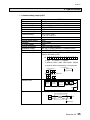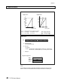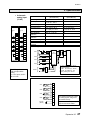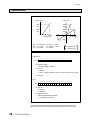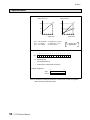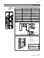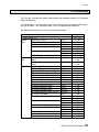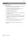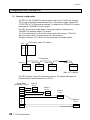
1
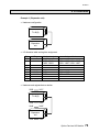
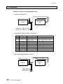
6F3B0251 UM-TS01∗∗∗-E002 PROGRAMMABLE CONTROLLER PROSEC USER’ S MANUAL − Expansion I/O − Main Menu Contents TOSHIBA CORPORATION T1/T1S 6F3B0251 Important Information Misuse of this equipment can result in property damage or human injury. Because controlled system applications vary widely, you should satisfy yourself as to the acceptability of this equipment for your intended purpose. In no event will Toshiba Corporation be responsible or liable for either indirect or consequential damage or injury that may result from the use of this equipment. No patent liability is assumed by Toshiba Corporation with respect to use of information, illustrations, circuits, equipment or examples of application in this publication. Toshiba Corporation reserves the right to make changes and improvements to this publication and/or related products at any time without notice. No obligation shall be incurred other than as noted in this publication. This publication is copyrighted and contains proprietary material. No part of this book may be reproduced, stored in a retrieval system, or transmitted, in any form or by any means electrical, mechanical, photocopying, recording, or otherwise without obtaining prior written permission from Toshiba Corporation. © TOSHIBA Corporation 1996. All rights reserved PROSEC and TOSLINE are registered trademarks of TOSHIBA Corporation. Publication number: UM-TS01∗∗∗-E002 1st edition July 1996, 3rd edition Dec. 1998 6F3B0251 Safety Precautions This manual is prepared for users of Toshiba’s Programmable Controller T1/T1S. Read this manual thoroughly before using the T1/T1S. Also, keep this manual and related manuals so that you can read them anytime while the T1/T1S is in operation. Hazard Classifications In the manuals related to the T1/T1S, the following two hazard classifications are used to explain the safety precautions. ! WARNING Indicates a potentially hazardous situation which, if not avoided, could result in death or serious injury. ! CAUTION Indicates a potentially hazardous situation which, if not avoided, may result in minor or moderate injury. It may also be used to alert against unsafe practices. Even a precaution is classified as CAUTION, it may cause serious results depending on the situation. Observe all the safety precautions described on this manual. Safety Precautions ! CAUTION • Turn off power to the T1/T1S before removing or mounting the option card or I/O module. Failure to do so can cause electrical shock or damage to the product. • Read the Safety Precautions described in the “T1/T1S User’s Manual − Basic Hardware and Function −” before using the option cards and the I/O modules. • Follow the instructions described in this manual and in the “T1/T1S User’s Manual − Basic Hardware and Function −” when installing and wiring the option cards or I/O modules. • The option cards and I/O modules have been designed for the T1/T1S. Use your option cards or I/O modules only with the T1/T1S. • Do not touch electronic components on the printed circuit board of the option cards or I/O modules. It may cause damage to the product. • Use attached screw (puller) for removing the option card. Do not pull I/O cable for removing the option card. It can cause unsafe situation because of cable disconnection. Expansion I/O 1 6F3B0251 About This Manual About This Manual This manual explains the specifications and operations of the expansion I/Os (option cards, expansion units and T2 type I/O modules) which are used with the T1/T1S. The TOSLINE-F10 data link card is also covered in this manual. For your better understanding of the T1/T1S, read the following manual at first to understand the T1/T1S system, then read this manual. T1/T1S User’ s manual − Basic Hardware and Function − UM-TS01∗∗∗-E001 Terminology The following is a list of abbreviations and acronyms used in this manual. µs ASCII AWG CPU CRC EEPROM H I/O LED ms RAM ROM Vac Vdc 2 microsecond American Standard Code For Information Interchange American Wire Gage Central Processing Unit Cyclic Redundancy Checking Electrically Erasable Programmable Read Only Memory hexadecimal (when it appears in front of an alphanumeric string) Input/Output Light Emitting Diode millisecond Random Access Memory Read Only Memory AC voltage DC voltage T1/T1S User’ s Manual 6F3B0251 Contents Contents Safety Precautions .................................................................................. 1 About This Manual ........................................................................................ 2 1. System Configuration ..................................................................... 5 1.1 1.2 1.3 1.4 1.5 1.6 T1/T1S system configuration ............................................................. Using the option card ........................................................................ Using the expansion unit .................................................................... Using the T2 I/O module .................................................................... Power capacity consideration ............................................................ Optional items .................................................................................... 6 8 9 11 13 14 2. Specifications .................................................................................. 15 2.1 2.2 2.3 Option card ........................................................................................ Expansion unit ................................................................................... T2 I/O module .................................................................................... 16 26 31 3. Installation ........................................................................................ 59 3.1 3.2 3.3 3.4 Mounting the option card ................................................................... Connecting the expansion unit .......................................................... Connecting the expansion rack ......................................................... Mounting the I/O module ................................................................... 60 62 63 64 4. I/O Allocation ................................................................................... 65 4.1 4.2 4.3 I/O allocation overview ...................................................................... I/O allocation methods ...................................................................... Register assignment ......................................................................... 66 69 70 5. Supplement for TOSLINE-F10 ......................................................... 79 5.1 5.2 5.3 Network configuration ........................................................................ Register assignment ......................................................................... RAS information ................................................................................ 80 81 82 Expansion I/O 3 6F3B0251 4 T1/T1S User’s Manual 6F3B0251 Section 1 System Configuration 1.1 1.2 1.3 1.4 1.5 1.6 T1/T1S system configuration, 6 Using the option card, 8 Using the expansion unit, 9 Using the T2 I/O module, 11 Power capacity consideration, 13 Optional items, 14 Expansion I/O 5 6F3B0251 1. System Configuration 1.1 T1/T1S system configuration The following figure shows the T1/T1S system configuration. Peripheral tool IBM-PC compatible personal computer T1 basic unit T1-16 Scope of this manual T1-28 Option cards T-PDS software T1-40 Handy programmer HP911A Expansion unit T1-40S Computer link function MMI/SCADA system Expansion rack T2 I/O modules 2-slot 6 T1/T1S User’s Manual 4-slot 6F3B0251 1. System Configuration The T1-16 and the T1-28 are fixed I/O points controllers. The T1-40 and T1-40S, however, have I/O expandability. There are three ways to expand its I/O points. They are using the option card, using the expansion unit, and using the T2 type I/O module. The option card is an I/O expansion card for the T1-40/T1-40S. It is approximately 1/2 the size of a credit card. The T1-40/T1-40S can hold up to two option cards. The expansion unit is a fixed I/O points expansion unit. Its size is the same as the T1-40/T1-40S. The T1-40/T1-40S can be connected to a 2-slot or 4-slot expansion rack allowing it to use most T2 I/O modules. Either one expansion unit or one expansion rack can be connected with the T1-40 /T1-40S. The option card can be used together with the expansion unit or the expansion rack. This manual explains the specifications of the option cards, the expansion unit and the I/O modules, and how to use them with the T1-40/T1-40S. Regarding the I/O expandability, there is no difference between the T1-40 and the T1-40S. Therefore, in this manual, T1-40 and T1-40S are called as T1-40(S) for ease of explanation. Expansion I/O 7 6F3B0251 1. System Configuration 1.2 Using the option card The T1-40(S) has two slots for mounting the option cards on the right side of the unit. The following eight types of the option cards are available. Type DI116 DO116 DD116 AD121 AD131 DA121 DA131 FR112 T1/T1 S-40 Description 16 points input, 24 Vdc - 5 mA 16 points output, 24 Vdc - 100 mA 8 points input, 24 Vdc - 5 mA + 8 points output, 24 Vdc - 100 mA 1 channel analog input 0-5V/0-20mA 1 channel analog input ±10V 1 channel analog output 0-20mA 1 channel analog output ±10V TOSLINE-F10 remote station, 1 word input + 1 word output Power supply Supplied from the basic unit (5 Vdc). See section 1.5. Option card • Up to two option cards can be installed. • The TOSLINE-F10 card (FR112) can be used together with other option card. However, two FR112s cannot be used at a time. • Cable side connector for the discrete I/O card (DI116, DO116 or DD116) is not supplied with the option card. This connector is separately available. See section 1.6. • A screw (puller) for removing the option card from the T1-40(S) is attached to the option card. 8 T1/T1S User’s Manual 6F3B0251 1. System Configuration 1.3 Using the expansion unit The T1-40(S) has an expansion connector for connecting the expansion unit or the expansion rack on the right side of the unit. The expansion unit has 32 points I/O (16 inputs and 16 outputs). Two types of the expansion unit are available. They are T1-EDR32 (DC input type) and T1-EAR32 (AC input type). Either one expansion unit can be connected to the T1-40(S). T1-40(S) right side view Expansion connector for expansion unit or expansion rack Option card slot cover The following two types of the expansion unit are available. Type T1-EDR32 T1-EAR32 T1-40(S) Input: Output: Input: Output: Description 16 points, 24 Vdc - 7 mA 16 points, relay, 240 Vac/24 Vdc (max.) - 2 A/point (max.) 16 points, 100 to 120 Vac - 7 mA 16 points, relay, 240 Vac/24 Vdc (max.) - 2 A/point (max.) Power supply Supplied from the basic unit (5Vdc). See section 1.5. Expansion unit Note) Only one expansion unit can be connected. Expansion I/O 9 6F3B0251 1. System Configuration External feature of the expansion unit Input terminals Input status LEDs Mounting hole IN PROSEC TOSHIBA T1 EDR40 OUT Output terminals Expansion connector Power LEDs (PWR and 24VDC) Output status LEDs Status LEDs: Name PWR (Power) 24VDC Input status LEDs Output status LEDs Color Green Green Red Red Function Lit when 5 Vdc supplied from the basic unit is normal. Lit when external 24 Vdc for output relay coil is normal. Lit when the corresponding input signal is ON. Lit when the corresponding output signal is ON. • Either one expansion unit or one expansion rack can be connected with the T1-40(S). • A 0.5 m expansion cable is supplied with the expansion unit. • Output relay coil power (24Vdc) is required on the expansion unit. • DIN rail bracket is provided on the expansion rack. 10 T1/T1S User’s Manual 6F3B0251 1. System Configuration 1.4 Using the T2 I/O module The T1-40(S) has an expansion connector for connecting the expansion unit or the expansion rack on the right side of the unit. The expansion rack is used for connecting T2 I/O modules with the T1-40(S). Two types of the expansion racks are available. They are 2-slot rack and 4-slot rack. Either one expansion rack can be connected to the T1-40(S). By using the expansion rack, the T1-40(S) can control up to 2 or up to 4 T2 I/O modules. The following two types of the expansion racks are available. Type BU152 BU154 Description Two I/O modules can be mounted (2-slot rack) Four I/O modules can be mounted (4-slot rack) BU152 (2-slot) Power supply Supplied from the basic unit (5 Vdc). See section 1.5. BU154 (4-slot) Expansion connectors • Either one expansion unit or one expansion rack can be connected with the T1-40(S). • A 0.2 m expansion cable is supplied with the expansion rack. • No power supply module is required on the expansion rack. • Expansion connectors are provided on the both sides. However either one can be used at a time. • DIN rail bracket is not provided on the expansion rack. Expansion I/O 11 6F3B0251 1. System Configuration The list below shows the I/O modules available for the T1-40(S). Type DI31 DI32 DI235 IN51 IN61 RO61 Name DC/AC input DC input AC input Relay output RO62 RO263 DO31 Transistor output (current sink) DO32 DO235 DO233P AC61 AI21 AI22 AI31 AI32 AO31 AO22 AO32 PI21 MC11 CF211 Transistor output (current source) Triac output Analog input Analog output Pulse input Positioning Communication interface Specifications 16 points (16 points/common), 12 to 24 Vdc/Vac 32 points (4 × 8 points/common), 24 Vdc 64 points (8 × 8 points/common), 24 Vdc 16 points (16 points/common), 100 to 120 Vac 16 points (16 points/common), 200 to 240 Vac 12 points (3 × 4 points/common), 240 Vac/24 Vdc (max.), 2 A/point, 4 A/common (max.) 8 points (isolated), 240 Vac/24 Vdc (max.), 2 A/point (max.) 16 points (2 × 8 points/common), 240 Vac/24 Vdc (max.), 2 A/point, 8 A/commom (max.) 16 points (16 points/common), 5 to 24 Vdc, 1 A/point, 1.2 A/4 points (max.) 32 points (4 × 8 points/common), 5 to 24 Vdc, 0.1 A/point (max.) 64 points (8 × 8 points/common), 5 to 24 Vdc, 0.1 A/point (max.) 16 points (16 points/common), 5 to 24 Vdc, 1 A/point, 1.2 A/4 points (max.) 12 points (3 × 4 points/common), 100 to 240 Vac, 0.5 A/point, 0.6 A/SSR (max.) 4 channels, 1 to 5 V / 4 to 20 mA, 8-bit resolution 4 channels, 1 to 5 V / 4 to 20 mA, 12-bit resolution 4 channels, 0 to 10 V, 8-bit resolution 4 channels, ±10 V, 12-bit resolution 2 channels, 1 to 5 V / 4 to 20 mA / 0 to 10 V, 8-bit resolution 2 channels, 1 to 5 V / 4 to 20 mA, 12-bit resolution 2 channels, ±10 V, 12-bit resolution 1 channel (2-phase and zero marker), 5/12 V, 100 kHz (max.), 24-bit counter 1 axis, 200 kHz (max.), 5 to 24 Vdc, ±999999 pulses 1 port of RS-232C, full-duplex, ASCII code, 300 / 600 / 1200 / 2400 / 4800 / 9600 / 19200 bps • Internal 5 Vdc power required for the I/O modules is supplied from the T1-40(S) basic unit. See section 1.5. 12 T1/T1S User’s Manual 6F3B0251 1. System Configuration 1.5 Power capacity consideration The T1-40(S) basic unit supplies internal 5 Vdc for option cards and/or I/O modules. The internal 5 Vdc output capacity of the T1-40(S) basic unit is as follows. T1-40(S) basic unit 5 Vdc output capacity When both the handy programmer (HP911A) and the RS-485 port (T1-40S) are used When the handy programmer (HP911A) is used When the T1-40S’s RS-485 port is used When neither the handy programmer (HP911A) nor the RS-485 port is used 700 mA 800 mA 900 mA 1000 mA The table below shows the maximum current consumption of 5 Vdc power of each card/module. When using the option cards, expansion unit and/or I/O modules, confirm that the total current consumption is within the T1-40(S)’s output capacity. Option card / Expansion unit / I/O module Option card Expansion unit I/O module 16 points DC input 16 points DC output Combination 8 inputs and 8 outputs 1 channel analog input 0-5V/0-20mA 1 channel analog input ±10V 1 channel analog output 0-20mA 1 channel analog output ±10V TOSLINE-F10 remote station 24 Vdc input/relay output 100-120Vac input/relay output 16 points DC/AC input 32 points DC input 64 points DC input 16 points AC input (100 - 120 Vac) 16 points AC input (200 - 240 Vac) 12 points relay output 8 points isolated relay output 16 points relay output 16 points transistor output (sink) 32 points transistor output (sink) 64 points transistor output (sink) 16 points transistor output (source) 12 points triac output 4 channels analog input (8-bit) 4 channels analog input (12-bit) 2 channels analog output (8-bit) 2 channels analog output (12-bit) 1 channel pulse input 1 axis position control Communication interface DI116 DO116 DD116 AD121 AD131 DA121 DA131 FR112 T1-EDR32 T1-EAR32 DI31 DI32 DI235 IN51 IN61 RO61 RO62 RO263 DO31 DO32 DO235 DO233P AC61 AI21 AI31 AI22 AI32 AO31 AO22 AO32 PI21 MC11 CF211 5 Vdc current consumption (max.) 50 mA 50 mA 50 mA 260 mA 260 mA 350 mA 240 mA 100 mA 120 mA 120 mA 15 mA 80 mA 100 mA 15 mA 15 mA 50 mA 40 mA 80 mA 60 mA 250 mA 250 mA 60 mA 300 mA 50 mA 50 mA 50 mA 50 mA 70 mA 170 mA 170 mA 80 mA 200 mA 550 mA Expansion I/O 13 6F3B0251 1. System Configuration 1.6 Optional items The following optional items related to the option cards, the I/O modules and expansion unit are available. Item Option card I/O connector Empty slot cover Expansion rack cable Expansion unit cable Type PT15S PT15F EX10∗ABP1 CS1R2 CS1R5E Description Cable side connector for DI116, Soldering type DO116, or DD116 Flat cable type For covering empty slot on the expansion rack For connecting the expansion rack, 0.15 m length (spare parts) For Connecting the expansion unit, 0.5m length (spare parts) Note) The I/O connector (cable side connector) for the discrete I/O option card (DI116, DO116 or DD116) is also available on the market. Refer to the followings. Connector maker: Fujitsu (1) Card side (PWB side) connector Type: FCN-365P024-AU (2) Cable side connector [soldering type] Type: FCN-361J024-AU (connector) Type: FCN-360C024-E (cover) (3) Cable side connector [flat cable type] Type: FCN-367J024-AU/F Use above (2) or (3). 14 T1/T1S User’s Manual 6F3B0251 Section 2 Specifications 2.1 Option card, 16 2.2 Expansion unit, 28 2.3 T2 I/O module, 31 Expansion I/O 15 6F3B0251 2. Specifications 2.1 Option card • 16 points DC input Item Card type I/O allocation type Number of input points Rated input voltage Rated input current Minimum ON voltage Maximum OFF voltage ON delay time OFF delay time De-rating condition Input signal display External connection Withstand voltage Current consumption Internal circuit DI116 DC input, current sourcing/sinking X 1W (1 input register XW assigned) 16 points (8 points/common) 24 Vdc, +10/-15 % 5 mA (at 24 Vdc) 18.0 Vdc 6.0 Vdc 10 ms 10 ms See Note on the next page None 24-pin connector 1500 Vac, 1 minute (internal ↔ external circuits) Max. 50 mA (5 Vdc) 0 1 7 COM0 8 F COM1 16 T1/T1S User’s Manual Internal circuit 6F3B0251 2. Specifications Item Terminal connection B DI116 A 12 1 + B A NC F 12 11 12 COM1 11 E D 10 10 B 9 9 9 8 8 8 NC 7 7 NC NC 6 6 NC 7 5 5 4 4 6 5 3 3 4 3 2 2 2 1 1 1 0 + C A + NC COM0 + When input register XW n is assigned; Input 0 ... Xn0 (n is register address) Input 1 ... Xn1 Input F ... XnF Note) As for the DC input, there is the following de-rating condition for maximum number of simultaneous ON points, depending on the ambient temperature. Simultaneous ON points (per common) 8 4 0 10 20 30 40 50 60 Ambient temperature [°C] Expansion I/O 17 6F3B0251 2. Specifications • 16 points DC output Item Card type I/O allocation type Number of output points Rated load voltage Maximum load current Voltage drop at ON Leakage current at OFF ON delay time OFF delay time Output signal display External connection Withstand voltage Current consumption Internal circuit DO116 Transistor output, current sinking Y 1W (1 output register YW assigned) 16 points (8 points/common) 5 to 24 Vdc, +10/-5 % 100 mA/point (at 24 Vdc), 20 mA/point (at 5 Vdc), 800 mA/common 0.4 V or less 100 µA 1 ms 2 ms None 24-pin connector 1500 Vac, 1 minute (internal ↔ external circuits) Max. 50 mA (5 Vdc) Vin0 0 Internal circuit 1 7 COM0 Vin1 8 F COM1 18 T1/T1S User’s Manual 6F3B0251 2. Specifications Item Terminal connection B DO116 A + 12 1 + B A COM1 12 F 11 12 Vin1 11 E D 10 10 B 9 9 9 8 8 8 NC 7 7 NC NC COM0 6 6 5 5 NC Vin0 7 4 4 6 5 3 3 4 3 2 2 2 1 1 1 0 C A When output register YW n is assigned; Output 0 ... Yn0 (n is register address) Output 1 ... Yn1 Output F ... YnF Expansion I/O 19 6F3B0251 2. Specifications • 8 points DC input and 8 points DC output combined Item Card type I/O allocation type Number of input points Rated input voltage Rated input current Minimum ON voltage Maximum OFF voltage ON delay time OFF delay time De-rating condition Number of output points Rated load voltage Maximum load current Voltage drop at ON Leakage current at OFF ON delay time OFF delay time I/O signal display External connection Withstand voltage Current consumption Internal circuit DD116 DC input (current sinking/sourcing), Transistor output (current sinking), combined X+Y 2W (1 input XW and 1 output YW registers assigned) 8 points (8 points/common) 24 Vdc, +10/-15 % 5 mA (at 24 Vdc) 18.0 Vdc 6.0 Vdc 10 ms 10 ms See Note on the next page 8 points (8 points/common) 5 to 24 Vdc, +10/-5 % 100 mA/point (at 24 Vdc), 20 mA/point (at 5 Vdc), 800 mA/common 0.4 V or less 100 µA 1 ms 2 ms None 24-pin connector 1500 Vac, 1 minute (internal ↔ external circuits) Max. 50 mA (5 Vdc) 0 Internal circuit 1 DC input 7 COM0 Vin1 0 1 7 COM1 20 T1/T1S User’s Manual DC output 6F3B0251 2. Specifications Item Terminal connection B DD116 A + B A COM1 12 7 11 12 Vin1 11 6 5 10 10 3 9 9 1 8 8 0 NC 7 7 NC NC 6 6 NC 7 5 5 + NC COM0 4 4 6 5 3 3 4 3 2 2 1 1 1 12 1 4 2 + 2 0 When input register XW n and output register YW n+1 is assigned; Input 0 ..... Xn0 (n is register address) Input 7 ...... Xn7 Output 0 ... Yn+10 (n+1 is next register address of n) Output 7 ... Yn+17 Note) As for the DC input, there is the following de-rating condition for maximum number of simultaneous ON points, depending on the ambient temperature. Simultaneous ON points (per common) 8 4 0 10 20 30 40 50 60 Ambient temperature [°C] Expansion I/O 21 6F3B0251 2. Specifications • 1 channel analog input (0-5V/0-20mA) Item Card type I/O allocation type Number of input points Resolution Rated input range Absolute max. input Rated input impedance Overall accuracy Conversion cycle External power supply Insulation I/O signal display External connection Withstand voltage Current consumption Input range setting (jumper plug JP1) Data format AD121 Analog input X 1W (1 input XW register assigned) 1 channel 12 bits (1/4000) 0-5V 0 - 20 mA ±7 V ±25 mA 1 MΩ or more 250 Ω ±0.5 % FS : 25°C ±1 % FS : 0 to 55°C 2ms None Photo-coupler None 2-pin removable connector 500 Vac, 1 minute (internal ↔ external circuits) Max. 260 mA (5 Vdc) Open Short (factory setting) Converts full scale analog input signal (0-20mA/ 0-5V) into digital data in 0 to 4000. F XW E D C B A 9 8 7 6 5 4 3 2 1 0 0 0 0 0 D D D D D D D D D D D D D: Data bit (12bits) 0 - 4000 (H0000 - H0FA0) 0-20mA: D=200 × A 0-5V: D = 800 × A A: Analog value D: Digital value 4000 Digital value 2000 0 Internal circuit 10 2.5 P AMP N 250Ω Terminal connection 20 (mA) Analog value 5 (V) AD conversion unit Photocoupler Internal circuit Jumper plug Shielded two-core twisted pair cable + ↑ P 2 N 1 V − Grounding 22 T1/T1S User’s Manual 6F3B0251 2. Specifications • 1 channel analog input (±10V) Item Card type I/O allocation type Number of input points Resolution Rated input range Absolute max. input Rated input impedance Overall accuracy Conversion cycle External power supply Insulation I/O signal display External connection Withstand voltage Current consumption Data format AD131 Analog input X 1W (1 input XW register assigned) 1 channel 12 bits (1/4000) ±10 V ±13 V 1 MΩ or more ±0.5 % FS : 25°C ±1 % FS : 0 to 55°C 2ms None Photo-coupler None 2-pin removable connector 500 Vac, 1 minute (internal ↔ external circuits) Max. 260 mA (5 Vdc) Converts full scale analog input signal (±10V) into digital data in -2000 to +2000. F XW E D C B A 9 8 7 6 5 4 3 2 1 0 S S S S S D D D D D D D D D D D S: Sign 0 = positive, 1 = negative D: Data bit (11bits) -2000 - 2000 (HF830 - H07D0) A negative value is expressed by 2’s complement D = 200 × A Digital value 2000 A: Analog value D: Digital value 1000 -10 -5 0 5 -1000 10 Analog value (V) -2000 Internal circuit P AMP N AD conversion unit Photocoupler Internal circuit AG Terminal connection Shielded two-core twisted pair cable + P 2 N 1 V − Grounding Expansion I/O 23 6F3B0251 2. Specifications • 1 channel analog output (0-20mA) Item Card type I/O allocation type Number of input points Resolution Rated input range Rated input impedance Overall accuracy Conversion cycle External power supply Insulation I/O signal display External connection Withstand voltage Current consumption Data format DA121 Analog output Y 1W (1 output YW register assigned) 1 points 12 bits (1/4000) 0 - 20 mA 600 Ω or less ±0.5 % FS : 25°C ±1 % FS : 0 to 55°C 2ms None Photo-coupler None 2-pin removable connector 500 Vac, 1 minute (internal ↔ external circuits) Max. 350 mA (5 Vdc) Converts digital data in 0 to 4000 into analog signal in full scale (0-20mA) F YW E D C B A 9 8 7 6 5 4 3 2 1 0 ∗ ∗ ∗ ∗ D D D D D D D D D D D D D: Data bit (12bits) 0 - 4000 (H0000 - H0FA0) ∗: No effect on D/A conversion A= 0.005 × D A: Analog value D: Digital value 20 Analog value (mA) 15 10 5 0 2000 4000 Digital value Internal circuit Internal circuit Photocoupler P DA conversion unit AMP BUF AG Terminal connection Shielded two-core twisted pair cable 2 P 1 N + Load − Grounding 24 T1/T1S User’s Manual N 6F3B0251 2. Specifications • 1 channel analog output (±10V) Item Card type I/O allocation type Number of output points Resolution Rated output range Rated output impedance Overall accuracy Conversion cycle External power supply Insulation I/O signal display External connection Withstand voltage Current consumption Data format DA131 Analog output Y 1W (1 output YW register assigned) 1 channel 12 bits (1/4000) ± 10V 10k Ω or more ±0.5 % FS : 25°C ±1 % FS : 0 to 55°C 2ms None Photo-couple None 2-pin removable connector 500 Vac, 1 minute (internal ↔ external circuits) Max. 240 mA (5Vdc) Converts digital data in -2000 to +2000 into analog signal in full scale (±10V) F E D C B A 9 8 7 6 5 4 3 2 1 0 YW S S S S S D D D D D D D D D D D S: Sign 0 = positive, 1 = negative D: Data bit (11bits) -2000 - 2000 (HF830 - H07D0) A negative value is expressed by 2’s complement Analog value (V) 10 5 -2000 -1000 0 1000 2000 -5 A = 0.005 X D A: Analog value D: Digital value Digital value -10 Internal circuit Internal circuit Photocoupler P DA conversion unit AMP BUF N AG Terminal connection Shielded two-core twisted pair cable 2 P 1 N + Load − Grounding Expansion I/O 25 6F3B0251 2. Specifications • TOSLINE-F10 remote station Item Card type I/O allocation type Transmission cable Configuration Transmission speed Transmission distance Transmission data capacity (cyclic scan) Scan cycle Error checking Register assignment Transmission speed Transmission line termination Receive data at transmission error Status display External connection Current consumption Jumper settings FR112 TOSLINE-F10 remote station TL-F (no I/O register assigned) Shielded twisted-pair cable Bus (party line) 750 kbps or 250 kbps Max. 500 m (750 kbps) Max. 1 km (250 kbps) Max. 32 words (512 points) 7 ms/32 words (750 kbps) 12 ms/32 words (250 kbps) CRC check SW34 ... Data send to the master SW35 ... Data receive from the master (2 words of transmission data shared) 750 kbps or 250 kbps, Jumper selection (JPS) Jumper selection (JPR) Previous data is held (TOSLINE-F10 error flag S00D comes ON) None 3-pin removable terminal block Max. 100 mA (5 Vdc) JPS Internal bus connector JPR Terminal block 1 2 3 JPS: Transmission speed JPR: Termination resistor 26 T1/T1S User’s Manual Rotary switch RSW1 Rotary switch RSW0 Open ... 750 kbps Short ... 250 kbps Open ... No connect Short ... Connect 6F3B0251 2. Specifications Item Station address setting FR112 RSW0 RSW1 0 0 Station address 10’s digit Station address 1’s digit Allowable station address: 0 to 30 Transmission cable connection Terminal block 1 2 3 L1 L2 SG Master station TERM T1 FR112 T1 FR112 T1 FR112 L1 L1 L1 L1 L2 L2 L2 L2 SG SG SG SG FG Connect externally Set JPR ON for termination Note) Refer to the TOSLINE-F10 manual for details of the TOSLINE-F10 system. Expansion I/O 27 6F3B0251 2. Specifications 2.2 Expansion unit • 16 points DC input and 16 points Relay output (T1-EDR32) • 16 points AC input and 16 points Relay output (T1-EAR32) Input specifications Item Input Specifications EDR32 Input type Input points Rated input voltage Rated input current Min. ON voltage Max. OFF voltage ON delay time OFF delay time Input signal display External connection Withstand voltage EAR32 DC input AC input 16 points (16 points/common) 24 Vdc, +10/-15% 100 - 120 Vac, +10/-15% 50/60 Hz 7 mA (at 24 Vdc) 7 mA (at 100 Vdc) 15 Vdc 80 Vac 5 Vdc 30 Vac 10 ms or less 25 ms or less 10 ms or less 30 ms or less LED display for all points, lit at ON, internal logic side Removable terminal block, M3.5 1500 Vac, 1 minute (between internal and external circuits) Internal circuit LED 0 F C 28 T1/T1S User’s Manual LED 0 Internal circuit F C Internal circuit 6F3B0251 2. Specifications Output specifications Item Output type Output points Rated load voltage Maximum load current ON resistance Leakage current at OFF Minimum load OFF delay time OFF delay time Output signal display External connection Withstand voltage Output Specifications EDR32 EAR32 Relay output, normally open 16 points (8 x isolated, 2 x 4 points/common) 240 Vac / 24 Vdc, +10% (max.) 2A/point (resistive), 4A/common 50 mΩ or less (initial value) None 5 Vdc, 10 mA (50 mW) 10 ms or less 10 ms or less LED display for all points, lit at ON, internal logic side Removable terminal block, M3.5 1500 Vac, 1 minute (between internal and external circuits) Internal circuit LED 24Vdc + Ry Internal circuit 10 10 17 17 18 1B C1 1C 1F C2 24Vdc - Expansion I/O 29 6F3B0251 2. Specifications Terminal connections 24 Vdc input 24 Vdc NC 1 NC C NC NC NC 0 3 2 5 4 7 6 9 B D F NC NC NC NC 8 A C E NC NC NC NC IN T1-EDR32 − NC 10 11 12 13 14 15 16 17 C1 19 1B 1C 1E OUT + NC NC 10 11 12 13 14 15 16 17 18 1A C2 1D 1F 24 Vdc + PS PS PS PS PS PS PS PS PS PS PS 240 Vac/ 24 Vdc (max.) Relay output 100 - 120 Vac input 100 - 120 Vac ∼ NC 1 NC C NC NC NC 0 3 2 5 4 7 6 9 B D F NC NC NC NC 8 A C E NC NC NC NC IN T1-EAR32 − NC 10 11 12 13 14 15 16 17 C1 19 1B 1C 1E OUT + NC NC 10 11 12 13 14 15 16 17 18 1A C2 1D 1F 24 Vdc + PS PS PS PS PS PS PS PS PS Relay output 30 T1/T1S User’s Manual PS PS 240 Vac/ 24 Vdc (max.) 6F3B0251 2. Specifications 2.3 T2 I/O module • 16 points DC/AC input DI31 01234567 89ABCDEF 0 1 2 3 4 5 6 7 8 9 A B C D E F Item Input Voltage Minimum ON Voltage Maximum OFF Voltage Input Current Number of Input Points ON Delay N Mode H Mode OFF Delay N Mode H Mode Withstand Voltage Current Consumption DI31 (EX10*MDI31) 12 - 24 V dc/ac, +10/-15 % (DC or 50/60 Hz) 9.6 V 3.6 V (leakage current 0.7 mA or less) Approx. 8 mA (at 24 Vdc) (typ.) 16 points (single common) 10 ms or less (dc) / 20 ms or less (ac) 1.5 ms or less (dc) 10 ms or less (dc) / 15 ms or less (ac) 1.5 ms or less (dc) 1500 Vac for 1 minute 15 mA (5 Vdc) or less Circuit Configuration Filter Selection 0 H Internal circuit N COM 1 2 LED display 12-24Vac/dc IN F COM COM Filter selection (jumper plug) N: Standard DC/AC input (factory setting) H: High-speed, DC input only Terminal Connections 0 1 2 3 4 5 7 9 B D 6 8 A C E F •œ COM 12-24V Expansion I/O 31 6F3B0251 2. Specifications • 32 points DC input Item DI32 CN1 1 2 3 4 5 6 7 89ABCDEF 1 2 3 4 5 6 7 89ABCDEF CN2 CN1 B A CN2 A B 12 1 DI32 (EX10*MDI32) 24 Vdc, +10/-15 % 18.0 V 6.0 V Approx. 5 mA (at 24 Vdc) (typ.) 32 points 10 ms or less 1.5 ms or less 10 ms or less 1.5 ms or less 2 x 24-pin connectors 4 Input Voltage Minimum ON Voltage Maximum OFF Voltage Input Current Number of Input Points ON Delay N Mode H Mode OFF Delay N Mode H Mode External Connections Common Number of Configuration Commons Input Points per Common Common Polarity Withstand Voltage Current Consumption 8 points/common No Polarity 1500 Vac for 1 minute 80 mA (5 Vdc) or less Circuit Configuration LED display 12 1 0 Input filter constant can be selected for each 16 points (CN1, CN2) by DIP switches. Factory setting: N mode Internal circuit 1 24Vdc IN Switch 1 (for CN1) 2 (for CN2) 7 COM OFF N mode N mode ON H mode H mode Terminal Connections CN1 (XWn) CN2 (XWn+1) + NC F B A 12 12 11 11 D 10 9 9 NC NC 0 + E 2 C 4 A 6 10 B 9 COM1 8 8 7 7 8 NC + + NC 6 6 5 5 4 4 4 C 3 3 3 2 E 1 2 2 0 1 1 7 5 6 1 2 2 3 3 4 4 5 5 NC 6 6 NC + 7 7 NC 9 8 8 A 9 9 10 10 F + COM3 11 11 12 12 NC 1 3 5 7 8 COM0 NC B 1 COM2 + NC NC A B D Note) Cable side connectors (soldering type) are attached as standard. 32 T1/T1S User’s Manual 6F3B0251 2. Specifications • 64 points DC input Item DI235 01234567 89ABCDEF 1 2 3 4 CN1 B A CN2 A B 20 1 Input Voltage Input Current Input Impedance Minimum ON Voltage Maximum OFF Voltage ON Delay OFF Delay External Connections Common Number of Configuration Commons Input Points per Common Common Polarity Derating Condition Withstand Voltage Current Consumption Circuit Configuration DI235 (TDI235**S) 24 Vdc, +10/-15 % Approx. 4 mA (at 24 Vdc) (typ.) 5.8 kΩ (at 24 Vdc) 16 V 5V 10 ms or less 15 ms or less 2 x 40-pin connectors 8 8 points/common No Polarity See Note below 1500 Vac for 1 minute 100 mA (5 Vdc) or less LED display 0L 20 24Vdc IN CN1 CN2 7L LC0 8L LC1 0H HC0 8H HC1 Internal Circuit 1 0L LC0 8L LC1 0H HC0 8H HC1 Note) Derating condition: Number of input ON points (per 1 connector) 32 (100%) 21.6Vdc or less 26 (80%) 20 (60%) 24Vdc 26.4Vdc Ambient temperature 0 10 20 30 40 50 60 Expansion I/O 33 6F3B0251 2. Specifications Terminal Connections CN2 (A)(B) CN1 (B)(A) 0L NC 20 20 NC PS PS NC 19 HC1 18 FH 17 EH 16 DH 15 CH 14 BH 13 AH 12 9H 11 8H 10 HC0 9 7H 8 6H 7 5H 6 4H 5 3H 4 2H 3 1H 2 0H 1 H 19 NC LC1 18 FL 17 EL 16 DL 15 CL 14 BL 13 AL 12 9L 11 8L 10 LC0 9 7L 8 6L 7 5L 6 4L 5 3L 4 2L 3 1L 2 0L 1 1L 2L PS 3L 4L 5L 6L 7L PS LC0 8L 9L AL PS BL CL DL EL FL PS LC1 1 1 2 2 3 3 4 4 5 5 6 6 7 7 8 8 9 9 10 10 11 11 12 12 13 13 14 14 15 15 16 16 17 17 18 18 L CN1 B A 1 2H 3H 4H 5H 6H 7H HC0 9H AH BH CH DH EH FH HC1 T1/T1S User’ s Manual PS H 1 20 : Power Supply 24 Vdc Note) Cable side connectors (soldering type) are attached as standard. 34 PS 8H CN2 A B PS CN1-L=XWn CN1-H=XWn+1 CN2-L=XWn+2 CN2-H=XWn+3 1H NC 19 19 NC NC 20 20 NC L 20 0H 6F3B0251 2. Specifications • 16 points AC input IN51 01234567 89ABCDEF 0 1 2 3 4 5 6 7 8 9 Item Input Voltage (Sine wave) Minimum ON voltage (Sine wave) Maximum OFF voltage (Sine wave) Input Current (Sine wave) Number of Input Points ON Delay (Sine wave) OFF Delay (Sine wave) Withstand Voltage Current Consumption IN51 (EX10*MIN51) 100 - 120 Vac, +10/-15 % (50/60 Hz) 80 Vac IN61 (EX10*MIN61) 200 - 240 Vac, +10/-15 % (50/60 Hz) 160 Vac 30 Vac 60 Vac (leak current 2 mA or less) (leak current 2 mA or less) Approx. 7 mA (100V-50Hz) Approx. 6 mA (200V-50Hz) 16 points (single common) 20 ms or less 15 ms or less 1500 Vac for 1 minute 15 mA (5 Vdc) or less 16 points (single common) 20 ms or less 15 ms or less 1500 Vac for 1 minute 15 mA (5 Vdc) or less Circuit Configuration 0 A B C D E F COM 100-120Vac IN Internal circuit 1 LED display 2 F COM COM Terminal connections 0 1 2 3 4 5 7 9 B D 6 8 A C E F ∗ •œ COM ∗ IN51: 100 - 120 Vac (50/60 Hz) IN61: 200 - 240 Vac (50/60 Hz) Expansion I/O 35 6F3B0251 2. Specifications • 12 points relay output RO61 01234567 89AB 0 1 2 3 C1 NC 4 Item RO61 (EX10*MRO61) Load Voltage 24 Vdc, +20 % (MAX) / 240 Vac, +10% (MAX) Maximum Load 2 A/point (resistive load), 1 A/point (inductive load), 4 A/4 points common Minimum Load 50 mW (5 V or more) Number of Output Points 12 points (4 points / common) ON Delay 10 ms or less OFF Delay 15 ms or less Leakage Current at OFF 0 mA Withstand Voltage 1500 Vac for 1 minute Over-current Protection None (required externally) Current Consumption 50 mA (5 Vdc) or less External Power Required 24 Vdc, +/-10% − 140 mA / all points ON for Relay Coil (10 mA / point) Circuit Configuration 5 6 7 LED display C2 + 8 9 A B 0 1 2 3 C1 4 Internal circuit C3 COIL 24Vdc 7 C2 + RELAY OUT 8 B C3 − Terminal Connections 0 1 3 2 C1 4 5 7 + 6 C2 8 9 24 Vdc B - A C3 Note) 1. ON/OFF life of relays: Electrical 100,000 times Mechanical 20 million times 2. No overload protection fuses are built into this module. Therefore make sure to insert fuses suitable to the load current. 36 T1/T1S User’s Manual 6F3B0251 2. Specifications • 8 points isolated relay output RO62 01234567 0 1 Item RO62 (EX10*MRO62) Load Voltage 24 Vdc, +20% (MAX) / 240 Vac, +10% (MAX) Maximum Load 2 A / point (resistive load), 1 A / point (inductive load) Minimum Load 50 mW (5 V or more) Number of Output Points 8 points (each point isolated) ON Delay 10 ms or less OFF Delay 15 ms or less Leakage Current at OFF 0 mA Withstand Voltage 1500 Vac for 1 minute Over-current Protection None (required externally) Current consumption 40 mA (5 Vdc) or less External Power Required 24 Vdc, +/-10% − 100 mA / all points ON for Relay Coil (10 mA / point) Circuit Configuration 2 LED display 3 Internal Circuit 4 0 5 1 6 2 7 24V dc RELAY OUT + − Terminal Connections 0 1 2 3 4 5 6 7 24 Vdc Note) 1. ON/OFF life of relays: Electrical 100,000 times Mechanical 20 million times 2. No overload protection fuses are built into this module. Therefore make sure to insert fuses suitable to the load current. Expansion I/O 37 6F3B0251 2. Specifications • 16 points relay output RO263 01234567 89ABCDEF 0 1 2 3 4 Item RO263 (TRO263**S) Load Voltage 24 Vdc, +25 % (MAX) / 240 Vac, +10% (MAX) Maximum Load 2 A / point (resistive load), 8 A / 8 points common Minimum Load 50 mW (5 V or more) Number of Output Points 16 points (8 points / common) ON Delay 10 ms or less OFF Delay 15 ms or less Leakage Current at OFF 0 mA Withstand Voltage 1500 Vac for 1 minute Over-current Protection None (required externally) Current Consumption 80 mA (5 Vdc) or less External Power Required 24 Vdc, +/-10% − 90 mA / all points ON for Relay Coil 5 6 Circuit Configuration 7 LED display COM0 8 9 A B C 0 1 Internal circuit D E F 7 COM1 + COM0 - 8 RELAY OUT F COM1 + - Terminal Connections 1 3 5 7 8 A C E COM1 0 2 4 6 COM0 9 B D F + 24 Vdc Note) 1. ON/OFF life of relays: Electrical 100,000 times Mechanical 20 million times 2. No overload protection fuses are built into this module. Therefore make sure to insert fuses suitable to the load current. 38 T1/T1S User’s Manual 6F3B0251 2. Specifications • 16 points transistor output DO31 01234567 89ABCDEF 0 1 2 3 4 5 6 7 8 9 A B C D E F Item DO31 (EX10*MDO31) Load Voltage 5 - 24 Vdc, +10/-5% (Internal current consumption 35 mA or less) Output Current 1 A / point (load voltage 7 V or more) 0.3 A / point (load voltage less than 7 V) 1.2A / 4 points (4-element transistor array) Output ON Resistance 1.5 Ω or less Number of Output Points 16 points (single common, current sinking) ON Delay 1 ms or less OFF Delay 1 ms or less Leakage Current at OFF 0.1 mA or less Withstand Voltage 1500 Vac for 1 minute Over-current Protection Built-in 5 A fuse (per common) Current Consumption 60 mA (5 Vdc) or less Circuit Configuration LED display + - Transistor array (4 circuits) Internal circuit 0 1 2 3 4 5-24Vdc OUT 8 C + Fuse − Common (5A) Terminal Connections 0 1 3 5 7 9 B D F − 2 4 6 8 A C E + 5 - 24 Vdc Expansion I/O 39 6F3B0251 2. Specifications • 32 points transistor output Item Load Voltage Output Current DO32 CN1 1 2 3 4 5 6 7 89ABCDEF 1 2 3 4 5 6 7 89ABCDEF CN2 CN1 B A CN2 A B 12 1 1 12 Voltage Drop at ON Number of Output Points ON Delay OFF Delay Leakage Current at OFF External Connections Common Number of configuration Commons Output Points per Common Common Polarity Withstand Voltage Over-current Protection Current Consumption DO32 (EX10*MDO32) 5 - 24 Vdc, +10/-5 % 100 mA / point (when load voltage 24 V) 20 mA / point (when load voltage 5 V) 800 mA / common 0.4 V or less 32 points (8 points/common, current sinking) 1 ms or less 2 ms or less 0.1 mA or less 2 x 24 pin connectors 4 8 points Minus common 1500 Vac for 1 minute Built-in 2 A fuse (per common) 250 mA (5 Vdc) or less Circuit Configuration Vin LED display Internal Circuit 0 5-24Vdc OUT 1 7 COM 2A Terminal Connections CN1 (YWn) + B COM1 C 12 F 11 D 10 B 9 9 8 NC A 12 11 Vin 0 E 2 C 4 10 9 A 6 8 Vin 8 NC NC NC NC Vin 8 7 7 6 6 5 5 6 A 4 4 4 C 3 3 3 2 E 1 2 2 0 1 1 NC + CN2 (YWn+1) COM0 C 7 5 Vin A B 1 1 2 2 3 3 4 4 1 3 5 7 COM2 5 5 6 6 NC 7 7 NC 9 8 8 9 9 10 10 F 11 11 12 12 + B D COM3 + Note) Cable side connectors (soldering type) are attached as standard. 40 T1/T1S User’s Manual 6F3B0251 2. Specifications • 64 points transistor output Item Load Voltage Output Current DO235 01234567 89ABCDEF 1 2 3 4 CN1 B A CN2 A B 20 1 1 20 Voltage Drop at ON Number of Output Points ON Delay OFF Delay Leakage Current at OFF External Connections Common Number of Configuration Commons Output Points per common Common Polarity Withstand Voltage Over-current Protection Current Consumption Circuit Configuration LED display DO235 (TDO235**S) 5 - 24 Vdc, +10/-5% 0.1 A / point (9.6 - 26.4 Vdc) 0.05 A / point (4.5 - 9.5 Vdc) 0.4 V or less 64 points (8 points/common, current sinking) 1 ms or less 1 ms or less 0.1 mA or less (24 Vdc) 2 x 40 pin connectors 8 8 points minus 1500 Vac for 1 minute None (required externally) 250 mA (5 Vdc) or less P24L0 0L Internal Circuit 5-24Vdc OUT 7L LC0 P24L1 8L LC1 P24H1 0H HC0 P24H1 8H HC1 P24L0 CN1 CN2 HC1 Expansion I/O 41 6F3B0251 2. Specifications Terminal Connections CN2 (A) (B) CN1 (B) (A) P24H1 HC1 FH EH DH CH BH AH 9H 8H P24H0 20 20 19 19 18 18 17 17 16 16 15 15 14 14 13 13 12 12 11 11 P24L1 0L LC1 1L FL 2L EL 3L DL 4L CL 5L BL 6L AL 7L 9L LC0 8L P24L0 P24L0 8L 10 10 HC0 7H 6H 5H 4H 3H 2H 1H 0H 9 9 8 8 7 7 6 6 5 5 4 4 3 3 2 2 1 1 H L LC0 9L 7L AL 6L BL 5L CL 4L DL 3L EL 2L FL 1L LC1 0L P24L1 1 2 2 3 3 4 4 5 5 6 6 7 7 8 8 9 9 10 10 11 11 12 12 13 13 14 14 15 15 16 16 17 17 18 18 19 19 20 1H 2H 3H 4H 5H 6H 7H HC0 P24H 08H 9H AH BH CH DH EH FH HC1 P24H 20 20 L CN1 B A CN1-L=XWn CN1-H=XWn+1 CN2-L=XWn+2 CN2-H=XWn+3 0H 1 H CN2 A B 1 : Load Power Supply 5-24Vdc 1 20 Note) Cable side connectors (soldering type) are attached as standard. 42 T1/T1S User’s Manual 6F3B0251 2. Specifications Item • 16 points transistor output Load Voltage (current source) DO233P 01234567 89ABCDEF 0 1 2 3 4 5 6 7 8 9 A B C D E F DO233P (TDO233P*S) 12 - 24 Vdc, +10/-5% (Internal current consumption 35 mA or less) Output Current 1 A / point 1.2A / 4 points (4-element transistor array) Output ON Resistance 1.5 Ω or less Number of Output Points 16 points (single common, current sourcing) ON Delay 1 ms or less OFF Delay 1 ms or less Leakage Current at OFF 0.1 mA or less Withstand Voltage 1500 Vac for 1 minute Over-current Protection Built-in 5 A fuse (per common) Current Consumption 60 mA (5 Vdc) or less Circuit Configuration LED display + Transistor array (4 circuits) Internal circuit 0 - 1 2 3 4 12-24Vdc OUT 8 C + Fuse (5A) Common − Terminal Connections 0 1 3 5 7 9 B D F − 2 4 6 8 A C E + 12 - 24 Vdc Expansion I/O 43 6F3B0251 2. Specifications • 12 points triac output AC61 01234567 89AB 0 1 2 3 C1 4 5 6 7 Item Load Voltage Output Current Voltage Drop at ON Number of Output Points ON Delay OFF Delay Leakage Current at OFF Withstand Voltage Over-current Protection Current Consumption AC61 (EX10*MAC61) 100 - 240 Vac, +10/-5 % (50/60 Hz sine wave) 0.5 A / point, 0.6 A (2-element SSR) 1.5 V or less (0.3 A load) 12 points (4 points / common) 1 ms or less 1/2 cycle of load power + 1 ms or less 1.2 mA (100 Vac) or less, 3 mA (240 Vac) or less 1500 Vac for 1 minute Built-in 2 A fuse (per common) 300 mA (5 Vdc) or less Circuit Configuration LED display 2-element SSR 0 Internal Circuit 1 C2 8 9 A B 2 3 C1 4 C2 C2 8 100-240Vac OUT fuse (2A) Terminal Connections 0 1 3 C1 5 7 C2 9 B C3 44 T1/T1S User’s Manual 2 C1 4 6 C2 8 A C3 C3 6F3B0251 2. Specifications • 4 channels analog input (8-bit) AI21 RUN 1P CH1 1N 1P CH2 1N 1P CH3 1N Item A121 A131 (EX10*MA121) (EX10*MA131) 1 - 5 V or 4 - 20 mA 0 - 10 V 1 - 5 V: 500 kΩ or more 500 kΩ or more 4 - 20 mA: 250 Ω 4 channels (N common) 4 channels (N common) Input Range Input Impedance Number of Input Points Resolution Overall Accuracy Conversion Cycle Wire Breakage Detection External Power Failure Detection Withstand Voltage Current Consumption External Power Required 8-bit (1/250) ±1 % (FS) Approx. 1 ms Yes, for 4-20mA 8-bit (1/250) ±1 % (FS) Approx. 1 ms No Yes Yes 1500 Vac for 1 minute 50 mA (5 Vdc) or less 12 - 24 Vdc, ±10 % 50 mA 1500 Vac for 1 minute 50 mA (5 Vdc) or less 12 - 24 Vdc, ±10 % 50 mA Circuit Configuration 1P CH4 1N 12-24Vdc + P − CH2 4-20mA/1-5V CH3 CH4 The AI21 type is set to 4 - 20 mA at the factory. For 1 - 5 V input, set J1 - J4 to V side. V CH1 12 - 24 Vdc A/D Converter I J1 N P Internal Circuit J2 N P N J3 P N J4 + − Power LED J1, J2, J3, and J4 jumper plugs are AI21 type only. • I side: for current (4 - 20 mA) • V side: for voltage (1-5 V) Factory setting is 4 - 20 mA. Terminal Connections CH1 P N CH2 P N CH3 P N CH4 P N + 12 - 24 Vdc (50mA) − Use shielded twisted-pair cables for analog signals, and ground the shields securely. Separate the external power (12 24 Vdc) line from other cables. Expansion I/O 45 6F3B0251 2. Specifications A/D Conversion Digital Value Digital Value 250 200 200 150 150 100 100 50 50 0 (a) (b) (c) 4 0 20 (mA) Analog value 10 (b) 250 (a) 1 (c) 10(V) Analog value 5 4 - 20 mA range: D = 15.625 x A - 62.5 1 - 5 V range: D = 62.5 x A - 62.5 0 - 10 V range: D = 25 x A D = Digital Value A = Analog Value Data Format F XW E D C B A 9 8 B ∗ ∗ ∗ ∗ ∗ ∗ ∗ D D D D D D D D 7 6 5 4 3 2 1 0 D: Data bit (8 bits) 0 to 250 (H00 to HFA) B: Error bit 0 = Normal 1 = Error with all D is 0, analog input line is open. (4 - 20 mA only) with all D is 1, external power (12 - 24 Vdc) is not normal. ∗: Always 0 Register assignment F XWn XWn+1 XWn+2 XWn+3 0 CH1 CH2 CH3 CH4 Note) In the voltage input mode, if the input terminals (P and N) are open, the input data is not 0. It is recommended to short the input terminals for unused input. 46 T1/T1S User’s Manual 6F3B0251 2. Specifications • 4 channels analog input (12-bit) AI22 RUN AI32 N P CH1 P CH2 N N N N P CH3 P CH4 N P CH2 P CH3 Input Range Input Impedance Number of Input Points Resolution Overall Accuracy RUN P CH1 Item N Conversion Cycle Wire Breakage Detection External Power Failure Detection Withstand Voltage Current Consumption External Power Required Circuit Configuration AI22 (EX10*MA122) 1 - 5 V or 4 - 20 mA 1 - 5 V: 1 MΩ or more 4 - 20 mA: 250 Ω 4 channels (N common) 12-bit (1/4000) ±0.5 % (FS) / 25°C ±1 % (FS) / 0 - 55°C Approx. 9.6 ms/4 channels Yes, for 4 - 20 mA AI32 (EX10*MA132) -10 to +10V 1 MΩ or more Yes No 1500 Vac for 1 minute 50 mA (5 Vdc) or less 24 Vdc, ±10% − 50 mA 1500 Vac for 1 minute 50 mA (5 Vdc) or less 24 Vdc, ±10% − 50 mA 4 channels (N common) 12-bit (1/4000) ±0.5 % (FS) / 25°C ±1 % (FS) / 0 - 55°C Approx. 9.6 ms/4 channels No P CH4 P N V I CH1 24Vdc+ 24Vdc+ - - CH2 4-20mA/1-5V • } 10V CH3 CH4 A/D Converter JI1 N P N JI2 P N P N JI3 JI4 JI1, JI2, JI3, JI4 (jumper plugs) are AI22 type only • I side: for current (4 - 20mA) • V side: for voltage (1 - 5V) Factory setting is 4 - 20 mA. + The AI22 type is set to 4-20 mA input at the factory. For 1-5 V input, set JI1 JI4 to V side. 24Vdc − LED DC/DC Converter Terminal Connections CH1 P N CH2 P N CH3 P N CH4 P N + 24 Vdc (50mA) − Use shielded twisted-pair cables for analog signals, and ground the shields securely. Separate the external power (24 Vdc) line from other cables. Expansion I/O 47 6F3B0251 2. Specifications A/D Conversion Digital Value Digital Value (a) 4000 4000 3000 3000 2000 2000 1000 1000 0 4 10 20 (mA) Analog Value -10 -5 (b) (c) 0 -1000 1 5 10 (V) Analog Value -2000 (a) 4 - 20 mA range: D = 250 x A - 1000 (b) 1 - 5 V range: D = 1000 x A - 1000 (c) ±10 V range: D = 200 x A D = Digital value A = Analog value Data Format • 4-20mA/1-5V F XW E D C B ∗ ∗ ∗ D D D D D D D D D D D D B A 9 8 7 6 5 4 3 2 1 0 D: Data bit (12 bits) 0 to 4000 (H0000 to H0FA0) B: Error bit 0 = Normal 1 = Error (analog input line is open or external power is not normal) ∗: Always 0 • ±10V F XW E D C B A 9 8 7 6 5 4 3 2 1 0 S S S S S D D D D D D D D D D D S: Sign bit 0 = Positive 1 = Negative D: Data bit (11 bits) -2000 to 2000 (HF830 to H07D0) 2’ s complement if negative Note) In the voltage input mode, if the input terminals (P and N) are open, the input data is not 0. It is recommended to short the input terminals for unused input. 48 T1/T1S User’s Manual 6F3B0251 2. Specifications • 2 channels analog output (8-bit) Item Output Range Load Impedance A031 RUN V 1P 1N CH 1P I 1N V 1P Number of Output Points Resolution Overall Accuracy Conversion Cycle External Power Failure Detection Withstand Voltage Current Consumption External Power Required AO31 (EX10*MA031) 0 - 10 V, 1 - 5 V, or 4 - 20 mA 5 V full-scale terminal: 5 kΩ or more 10 V full scale terminal: 10 kΩ or more 20 mA full-scale terminal: 600 Ω or less 2 channels (N side common) 8-bit (1/250) ±1 % (FS) Approx. 1 ms No 1500 Vac for 1 minute 70 mA (5 Vdc) or less 24 Vdc, ±10% − 90 mA 1N CH 1P I Circuit Configuration Jumper settings 1N 24Vdc + − D/A Converter CH1 J11 Internal circuit V1 I1 J2 5/10V 20mA V2 J1 CH2 J21 I1 The A031 type is set to 1 - 5 V, 4 - 20 mA setting at the factory. Refer to the circuit configuration for 0 - 10 V jumper setting. P N P N P N P N + 0V J1/J2: Offset J1 side = 1 V (4 mA) J2 side = 0 V (0 mA) (for both CH1 and CH2) J11: CH1 voltage gain Upper side = 5 V Lower side = 10 V J21: CH1 voltage gain Upper side = 5 V Lower side = 10 V 24 Vdc − Terminal Connections P N V1 CH1 P N I1 Note) Either voltage or current output can be used. P N V2 CH2 P N I2 Use shielded twisted-pair cables for analog signals, and ground the shields securely. 24Vdc (90mA) Separate the external power (24 Vdc) line from other cables. + − V: Voltage output I: Current output Expansion I/O 49 6F3B0251 2. Specifications D/A Conversion Analog Value (mA) Analog Value (V) (a) 20 10 5 4 1 0 (c) 10 (b) 0 50 100 150 200 250 50 100 150 200 250 Digital Value Digital Value (a) 4 - 20 mA range: A = 0.064 x D + 4 (mA) (b) 1 - 5 V range: A = 0.016 x D + 1 (V) (c) 0 - 10 V range: A = 0.04 x D (V) A = Analog value D = Digital value Data Format (2 output registers (YW) are assigned) YW F E D C B A 9 8 ∗ ∗ ∗ ∗ ∗ ∗ ∗ ∗ D D D D D D D D 7 6 5 4 3 2 1 0 D: Data bit (8 bits) 0 to 250 (H00 to HFA) ∗: Invalid (does not affect D/A conversion) Register assignment F YWn YWn+1 0 CH1 CH2 Note) If the direct I/O instruction (FUN 235) is used for this module, two registers (both channels) should be specified. 50 T1/T1S User’s Manual 6F3B0251 2. Specifications • 2 channels analog output (12-bit) AO22 AO32 RUN P V RUN CH1 P V N CH1 N P I N P V CH2 P V N CH2 N P I - Output Range Load Impedance Number of Output Points Resolution Overall Accuracy Conversion Cycle External Power Failure Detection Withstand Voltage Current Consumption External Power Required AO22 (EX10*MAO22) 1 - 5 V or 4 - 20 mA 1 - 5 V: 5 kΩ or more 4 - 20 mA: 600 Ω or less 2 channels (N side common) 12-bit (1/4000) ±0.5 % (FS) / 25°C ±1 % (FS) / 0~55°C Approx. 1 ms No AO32 (EX10*MAO32) -10 to +10V 5 kΩ or more 1500 Vac for 1 minute 170 mA (5 Vdc) or less 24 Vdc, ±10% − 90 mA 1500 Vac for 1 minute 170 mA (5 Vdc) or less 24 Vdc, ±10% − 90 mA 2 channels (N side common) 12-bit (1/4000) ±0.5 % (FS) / 25°C ±1 % (FS) / 0~55°C Approx. 1 ms No Circuit Configuration V1 CH1 N 24Vdc+ Item 24Vdc+ Internal circuit • D/A converter I1 ∗ • CH1 P N P N CH2 - V2 CH2 • 4-20mA/1-5V P N P N ±10V I2 ∗ • • • + • 24Vdc LED ∗ AO22 only − • DC / DCconverter Terminal Connections ∗ AO22 only P N V1 CH1 P N I1 ∗ Note) Either voltage or current output can be used. P N V2 CH2 P N ∗ Use shielded twisted-pair cables for analog signals, and ground the shields securely. 24Vdc (90mA) Separate the external power (24 Vdc) line from other cables. I2 + − V: Voltage output I: Current output Expansion I/O 51 6F3B0251 2. Specifications D/A Conversion Analog Value (V) Analog Value (mA) (a) 20 (c) 10 (b) 5 10 4 1 0 2000 -2000 4000 2000 0 4000 Digital Value Digital Value -5 -10 (a) 4 - 20 mA range: A = 0.004 x D + 4 (mA) (b) 1 - 5 V range: A = 0.001 x D + 1 (V) (c) ±10 V range: A = 0.005 x D (V) A = Analog value D = Digital value Data Format (2 output registers (YW) are assigned) • 4 - 20 mA / 1 - 5 V YW F E D C ∗ ∗ ∗ ∗ D D D D D D D D D D D D B A 9 8 7 6 5 4 3 2 1 0 D: Data bit (12 bits) 0 to 4000 (H0000 to H0FA0) ∗: Invalid (does not affect D/A conversion) • ±10 V YW F E D C B ∗ ∗ ∗ ∗ S D D D D D D D D D D D A 9 8 7 6 5 4 3 2 1 0 S: Sign bit 0 = Positive 1 = Negative D: Data bit (11 bits) -2000 to 2000 (HF830 to H07D0) 2’ s complement if negative Note) If the direct I/O instruction (FUN 235) is used for this module, two registers (both channels) should be specified. 52 T1/T1S User’s Manual 6F3B0251 2. Specifications • 1 channel pulse input Item PI21 (EX10*MP121) 12 V, +10/-20 % (12 V setting), 5 V, +10/-20 % (5V setting) 12 - 24 Vdc, +10/-15 % 9 V (12 V setting), 3.5 V (5 V setting) 9.6 V 2 V (12 V setting), 1 V (5 V setting) 3.6 V 12 V − 7.5 mA (12 V setting), 5V − 10 mA (5V setting) 24 V − 10 mA, 12 V − 5 mA 1 channel (phase A, B, M and EXT) 100 kpps (max.) (pulse-width 4 µs or more) 24-bit binary Phase A, B (90 degree phase shift), up/down Phase A: count up / phase B: count down Always count enable Both M and EXT are ON: Count enable Either M or EXT is OFF: Count stop (count value held) Count value is reset to 0 at the moment when both M and EXT are ON 5 ms or less 1500 Vac for 1 minute 80 mA (5 Vdc) or less Input Voltage A, B, M PI21 A EXT B +A -A +B -B +M -M EXT •u›u •u›u 12-24Vdc 5/12V PULSE IN EXT A, B, M EXT A, B, M EXT A, B, M EXT Number of Input Points Pulse Counting Speed Counter Configuration Pulse Input Quadrature Mode Up / down Counter Normal Operation Hold Mode Counter Reset Minimum ON Voltage Maximum OFF Voltage Input Current EXT Input ON/OFF Delay Withstand Voltage Current Consumption Circuit Configuration Input current flow The input voltage of A, B and M are set to 12 V, and the counter mode is set to quadrature normal count mode at the factory. +A -A +B -B +M -M A A5 A12 B5 B12 M5 M12•œ •œ BUD UNV B Counter BIP UPDW •œ • (Reset to 0 when power comes ON) Mode setting Input circuit • EXT Counter reset (edge detect) EXT • _5/_12 Jumper (Input voltage) _5: 5V input _12: 12V input Set all A, B and M to the same side. (5 V or 12 V) Shows the factory setting BIP/UPDW Jumper (Pulse input mode) BIP: Quadrature UPDW: Up/down BUD/UNV Jumper (Counter operation mode) BUD: Normal mode UNV: Hold mode Expansion I/O 53 6F3B0251 2. Specifications Terminal Connections +A 12 Vdc (5 Vdc) -A +B -B +M Pulse encoder -M Use shielded twisted-pair cables for pulse signals, and ground the shield securely. EXT 12 - 24 Vdc Wiring Example Encoder PI21 Power +A A -A +B B -B +M M -M EXT 0V 5 / 12 Vdc 12 - 24 Vdc Data Format Register assignment XWn F XWn+1 8 7 6 S S 223 0 F Count 0 Count 216 215 20 24-bit counter: Data range = -8388608 to 8388609 (HFF800000 to H007FFFFF) The counter works as a ring counter. If upper 8 bits of XWn is masked, the count data range is 0 to 16777215. Note) The double-word register arrangement of the PI21 and that of the T1 are different. In the T1 user program, exchange the upper and lower words as follows. [ XW00 MOV D0101 ][ XW01 MOV D0100 ] In this example, the PI21 is allocated to XW00 and XW01, and the count value is stored in double-word register D0101⋅D0100. 54 T1/T1S User’s Manual 6F3B0251 2. Specifications Pulse Input Mode < Quadrature > A B Count down Count up < Up/down > A B Count up Count down Counter Operation Mode < Normal mode > Up Phase A/B Down phase M EXT 8388607 Count value 0 -8388608 < Hold mode > Phase A/B Up Down phase M EXT (Holding) (Holding) Count value 0 Note) If the direct I/O instruction (FUN 235) is used for this module, two registers (both upper and lower words) should be specified. Expansion I/O 55 6F3B0251 2. Specifications • 1 axis position control MC11 PROGMR Number of Control Axes Control Units Control Range Point Data Capacity Maximum Speed Operation Speed RUN ZLS OT PLS CN A B PC 1 PROGMR 12 MC11 (EX10*MMC11) Item Acceleration / Deceleration System Acceleration / Deceleration Time Backlash Compensation Zero Position Offset Dwell Time I/O Allocation Type Parameter Storage Input Input Voltage Input Current ON / OFF Voltage ON / OFF Delay Output Pulse Mode Output (Switch setting) Output Method ON / OFF Delay RUN Output Method Output Operation Current Internal Consumption External 1 axis Pulse, inch, mm, etc. ±999,999 (units) 64 points 200 kpps Zero return speed, Maximum speed, Minimum speed Automatic trapezoidal / triangular system 0 to 26 s 0 to 1000 pulses ±999,999 units 0 to 99 s X+Y 4 W (2 XW and 2 YW registers) EEPROM 12 - 24 Vdc (Z-phase: 5 V or 12 - 24 V) 10 mA (at 24 Vdc) 9.6 V / 3.2 V 5 ms (Z-phase: 1 ms) (1) CW or CCW, Error counter clear (2) Pulse + Direction, Error counter clear Open collector (5 - 24 Vdc, 50mA) 2 µs Open collector (5 - 24 Vdc, 50mA) ON during normal operation 200 mA − 5 Vdc 400 mA − 5 Vdc (when HP100 connected) 100 mA − 12 - 24 Vdc Connector Pin Arrangement RUN output (0V) CW or Pulse output (0V) CCW or Direction output (0V) Error counter clear output (0V) Z-phase input (0V) Z-phase input (0V) Zero position switch input (-/+) HOLD input (-/+) Emergency stop input (-/+) CW over-travel limit input (-/+) CCW over-travel limit input (-/+) Power input (0V) A 1 2 3 4 5 6 7 8 9 10 11 12 B 1 2 3 4 5 6 7 8 9 10 11 12 RUN output (5-24Vdc) CW or Pulse output (5-24Vdc) CCW or Direction output (5-24Vdc) Error counter clear output (5-24Vdc) Z-phase input (5Vdc) Z-phase input (12-24Vdc) Zero position switch input (+/-) HOLD input (+/-) Emergency stop input (+/-) CW over-travel limit input (+/-) CCW over-travel limit input (+/-) Power input (12-24Vdc) Note) Cable side connector (soldering type) is attached as standard. 56 T1/T1S User’s Manual 6F3B0251 2. Specifications Input Circuit Z-phase input (5Vdc) : B5 Z-phase input (0V) : A5 Z-phase input (12-24Vdc) : B6 Z-phase input (0V) : A6 B7 • A7 • B8 • A8 • B9 • A9 • B10 • A10 • B11 • A11 • Zero position switch input (12/24Vdc) HOLD input (12/24Vdc) Emergency stop input (12/24Vdc) CW over-travel limit input (12/24Vdc) CCW over-travel limit input (12/24Vdc) Note) For the Z-phase input, use either 5 Vdc or 12 - 24 Vdc. Output Circuit Constant-voltage circuit • • • • B12 : Power input (12-24Vdc) • B1 : RUN output • A1 : RUN output (0V) • B2 : CW / Pulse output • A2 :CW / Pulse output (0V) • B3 : CCW / Direction output • A3 : CCW / Direction output (0V) • B4 : Error counter clear output • A4 : Error counter clear output (0V) • A12 : Power input (0V) • • • Expansion I/O 57 6F3B0251 2. Specifications • Communication interface Item Module Type I/O Allocation Type CF211 RESET CH1 CH1 CIF Buffer Memory Capacity Transmission Interface Transmission Mode Synchronizing Frame Format Transmission Speed Transmission Code Message Length Interface Connector Display Isolation Current Consumption Circuit Configuration I/O bus CF211 (TCF211**S) Serial communication interface module i X+Y 4W (2 input XW and 2 output YW registers assigned) 160 words × 2 (accessed from T1/T1S by READ/WRITE instruction) RS-232C, 1 channel Full-duplex Start-stop system (asynchronous) Start bit: 1 bit Data bits: 7 or 8 bits Parity: odd/even/none Stop bit: 1 or 2 bits (Total 10 or 11 bits) 300, 600, 1200, 2400, 4800, 9600 or 19200 bps ASCII Max. 320 bytes Dsub-9-pin female connector 1 LED display, lit when transmitting/receiving data None (between RS-232C port and internal logic) 550 mA (5 Vdc) or less 2 port buffer CPU RAM ROM I/O I/F RESET switch RS-232C interface Serial Interface Connection 1 2 RXD 3 TXD 4 DTR 5 SG 6 DSR 7 5Vdc TXD RXD DSR SG DTR 8 9 Note) DTR is ON while power to the T1/T1S is ON. Note) Refer to the CF211 manual for details. 58 T1/T1S User’s Manual TXD RXD DTR DSR SG 6F3B0251 Section 3 Installation 3.1 3.2 3.3 3.4 Mounting the option card, 60 Connecting the expansion unit, 62 Connecting the expansion rack, 63 Mounting the I/O module, 64 Option Card and I/O Module 59 6F3B0251 3. Installation 3.1 Mounting the option card ! CAUTION • Turn off power to the T1/T1S before removing or mounting the option card. Failure to do so can cause electrical shock or damage to the product. • Do not touch electronic components on the printed circuit board of the option card. It may cause damage to the product. • Use attached screw (puller) for removing the option card. Do not pull I/O cable for removing the option card. It can cause unsafe situation because of cable disconnection. (1) Remove the option card slot cover provided on the right side of the T1-40(S) as follows. Œ • The tool for opening the cover is attached on the back of the unit. Remove the tool from the unit. Ž Push the tool to unhook the cover. Then remove the cover. 60 T1/T1S User’s Manual Put the tool so that the marks ∆ on the tool and the unit are aligned. 6F3B0251 3. Installation (2) Insert the option card into the upper or lower slot. T1-40(S) right side view Upper slot connector Lower slot connector Internal bus connector Puller hole block Option card (3) Push the puller hole block of the option card until it reaches the end. When the internal bus connector is inserted correctly, it will make a click. (4) Cut off the window of the option card slot cover with clippers, and fix the cover to the T1-40(S) to lock the option card. Option card slot cover Cutting for DI116, DO116 or DD116 Cutting for FR112, AD121, AD131, DA121 or DA131 (5) When you remove the option card, use the attached screw (puller). Fix the screw (puller) to the puller hole block of the option card, and pull the screw (puller). Do not pull I/O cable to remove the option card. It can cause cable disconnection. Option Card and I/O Module 61 6F3B0251 3. Installation 3.2 Connecting the expansion unit ! CAUTION • Turn off power to the T1/T1S before connecting or removing the expansion unit. Failure to do so can cause electrical shock or damage to the product. • Cover the unused expansion connector by attached protective cover to prevent shortcircuit of the connector pins. (1) Remove the expansion connector cover provided on the right side of the T1-40(S) and the expansion unit. T1-40(S) or Expansion unit right side view Expansion connector (2) Connect the expansion unit with the T1-40(S) using the 0.5 m cable attached to the expansion unit. T1- 40(S) Expansion cable (0.5 m) Expansion unit 62 T1/T1S User’s Manual 6F3B0251 3. Installation 3.3 Connecting the expansion rack ! CAUTION • Turn off power to the T1/T1S before connecting or removing the expansion rack. Failure to do so can cause electrical shock or damage to the product. • Cover the unused expansion connector by attached protective cover to prevent shortcircuit of the connector pins. (1) Remove the expansion connector cover provided on the right side of the T1-40(S). T1-40(S) right side view Expansion connector (2) Connect the expansion rack with the T1-40(S) using the 0.15 m cable attached to the expansion rack. On the expansion rack, two expansion connectors are provided on the both sides. However, either one connector can be used at a time. Normally, the left side connector is used. Expansion rack T1-40(S) Expansion cable (0.15 m) Option Card and I/O Module 63 6F3B0251 3. Installation 3.4 Mounting the I/O module ! CAUTION • Turn off power to the T1/T1S before removing or mounting the I/O module. Failure to do so can cause electrical shock or damage to the product. • Do not touch electronic components on the printed circuit board of the I/O module. It may cause damage to the product. (1) Install I/O modules from the left slot, taking care to securely insert them into the slots of the expansion rack. (2) Insert the I/O module fully until both the upper and lower hooks of the of the I/O module are locked in the expansion rack. Expansion rack Mounting hook I/O module (3) To remove the I/O module from the expansion rack, push both the upper and lower hook levers and pull the I/O module. 64 T1/T1S User’s Manual 6F3B0251 Section 4 I/O Allocation 4.1 I/O allocation overview, 66 4.2 I/O allocation methods, 69 4.3 Register assignment, 70 Option Card and I/O Module 65 6F3B0251 4. I/O Allocation 4.1 I/O allocation overview The I/O allocation is the operation to let the T1-40(S) to recognize the type and location of the option cards, the I/O modules and/or the expansion unit which are connected to the T1-40(S). The T1-40(S) has the information called “I/O allocation table” in its memory. This “I/O allocation table” indicates what type of card/module/unit is connected on which mounting location. The contents of the I/O allocation table is as follows. Slot PU 0 1 2 3 4 5 6 7 I/O type X+Y 4W PU slot must be blank Slot 0 is for T1/T1S basic unit Slots 1 to 3 are for option cards Slots 4 and 5 are for expansion unit Slots 4 to 7 are for I/O modules The figure below shows the correspondence between I/O allocation “Slot” and hardware location. Basic unit = Slot 0 Expansion rack 4 5 6 7 Slot number T1-40(S) Expansion unit = Slot 4 and 5 Option card slot (upper) = Slot 1 Option card slot (lower) = Slot 2 Note 1) Slot 3 is dedicated for the TOSLINE-F10 remote station card (FR112). When the FR112 is used, it is allocated on the slot 3 regardless of physical mounting location (upper or lower slot). Note 2) When the 2-slot expansion rack (BU152) is used, slots 6 and 7 cannot be used. Note 3) The expansion unit occupies two slots (slots 4 and 5) by one unit. Note 4) The expansion rack and the expansion unit cannot be connected at the same time. 66 T1/T1S User’s Manual 6F3B0251 4. I/O Allocation The “I/O type” indicates the type of card/module and assigned number of I/O registers (XW/YW registers). “X” means input, “Y” means output, and “X+Y” means input and output mixture types. And, for example, “4W” means 4 words of XW/YW registers are assigned. The table below shows the “I/O type” of each card/module. Option card / I/O module T1-40(S) basic unit Option 16 points DC input card 16 points DC output 8 points input/8 points output 1 channel analog input (12-bit) 1 channel analog output (12-bit) TOSLINE-F10 remote station Expansion 16 points DC input/16 points relay unit output 16 points AC input/16 points relay output I/O module 16 points DC/AC input 32 points DC input 64 points DC input 16 points AC input (100 - 120 Vac) 16 points AC input (200 - 240 Vac) 12 points relay output 8 points isolated relay output 16 points relay output 16 points transistor output 32 points transistor output 64 points transistor output 16 points transistor output (source) 12 points triac output 4 channels analog input (8-bit) 4 channels analog input (12-bit) 2 channels analog output (8-bit) 2 channels analog output (12-bit) 1 channel pulse input 1 axis position control Communication interface DI116 DO116 DD116 AD121 AD131 DA121 DA131 FR112 T1-EDR32 T1-EAR32 DI31 DI32 DI235 IN51 IN61 RO61 RO62 RO263 DO31 DO32 DO235 DO233P AC61 AI21 AI31 AI22 AI32 AO31 AO22 AO32 PI21 MC11 CF211 I/O type X+Y 4W X 1W Y 1W X+Y 2W X 1W X 1W Y 1W Y 1W TL-F 1) X 1W 2) Y 1W X 1W 2) Y 1W X 1W X 2W X 4W X 1W X 1W Y 1W Y 1W Y 1W Y 1W Y 2W Y 4W Y 1W Y 1W X 4W X 4W X 4W X 4W Y 2W Y 2W Y 2W X 2W X+Y 4W iX+Y 4W 2) Option Card and I/O Module 67 6F3B0251 4. I/O Allocation Note 1) The FR112 has the I/O type “TL-F”. No XW/YW register is assigned to the FR112. For the FR112, special registers SW34 and SW35 are assigned, instead of XW/YW registers. See section 5. Note 2) The expansion unit requires two consecutive slots (slots 4 and 5) for I/O allocation. The slot 4 is “X 1W”, and slot 5 is “Y 1W””. Note 3) The I/O type of the CF211 has a prefix “i”. This “i” prefix functions to inhibit batch I/O refresh for the module. To add the “i” prefix for this modules, the manual I/O allocation operation is required. See section 4.2. 68 T1/T1S User’s Manual 6F3B0251 4. I/O Allocation 4.2 I/O allocation method The operation to create the I/O allocation table is called “I/O allocation”. When the T1-40(S) is used without connecting option card, I/O module nor expansion unit, the I/O allocation is not required. Because the I/O allocation table for basic unit is created automatically when the memory clear operation is performed. However, when option cards, I/O modules, and/or expansion unit are used, or T1/T1S’s user program is developed in off-line, the I/O allocation is necessary. There are two methods for the I/O allocation. Automatic I/O allocation: When the automatic I/O allocation command is executed from the programmer, the T1-40(S) checks the hardware configuration, then creates the I/O allocation table. This method is useful when all the necessary hardware (option cards, I/O modules and/or expansion unit) is prepared. Manual I/O allocation: I/O type can be set onto the I/O allocation table slot by slot by the programmer. (Editing of the I/O allocation table) This method is used when off-line programming is performed or special I/O type, such as “i” prefix or SP is used. The table below shows the available I/O type by the manual I/O allocation. Function type X Y X+Y iX iY iX+Y Blank SP TL-F Number of I/O registers assigned 01, 02, 04, 08, or 16 01, 02, 04, 08, or 16 02, 04, 08, or 16 01, 02, 04, 08, or 16 01, 02, 04, 08, or 16 02, 04, 08, or 16 01, 02, 04, 08, or 16 - Description For input For output For input and output mixture For input Batch I/O refresh For output is not executed For input and output mixture For vacant slot (no register is assigned) Used to assign YW registers for vacant slot For TOSLINE-F10 (no I/O register is assigned) NOTE (1) Do not use the I/O type other than the listed above for the T1/T1S. (2) To run the T1/T1S, the I/O allocation table and physical I/O configuration must be matched. Option Card and I/O Module 69 6F3B0251 4. I/O Allocation 4.3 Register assignment Once the I/O allocation table is created, the T1-40(S)’s registers are assigned to the hardware (card/module/unit) according to the following rules. (1) Input register (XW) and output register (YW) have consecutive register addresses. That is, one address is for either XW or YW. (2) XW registers are assigned to the I/O type “X”. (3) YW registers are assigned to the I/O type “Y”. (4) XW and YW registers are assigned to the I/O type “X+Y”. Leading half are XW and following half are YW. (5) I/O registers (XW/YW) are assigned sequentially from slot 0. (6) T1-40(S) basic unit has the I/O type “X+Y 4W”. Therefore, four registers (XW00, XW01, YW02 and YW03) are assigned to the basic unit. YW03 is assigned internally. (7) No register is assigned to a vacant slot. (8) Specified number of YW registers are assigned internally to the I/O type “SP”. (9) For “TL-F”, special registers SW34 and SW35 are assigned. The following pages show some examples of register assignment for some configuration. 70 T1/T1S User’s Manual 6F3B0251 4. I/O Allocation Example 1 (Option card) • Hardware configuration T1-40(S) Upper slot = DI116 (X 1W) Lower slot = DD116 (X+Y 2W) • I/O allocation table and register assignment Slot PU 0 1 2 3 4 5 6 7 I/O type Assigned register X+Y 4W X 1W X+Y 2W XW00, XW01, YW02, YW03 XW04 XW05, YW06 Assigned device X000 - X00F, X010 - X01F, Y020 - Y02F, Y030 - Y03F X040 - X04F X050 - X05F, Y060 - Y06F • Hardware and register/device relation X000 X017 T1-40(S) Y020 Y02F X040 - X04F (DI116) X050 - X057, Y060 - Y067 (DD116) Note) X018 to X01F, Y030 to Y03F, X058 to X05F, and Y068 to Y06F are assigned internally. Option Card and I/O Module 71 6F3B0251 4. I/O Allocation Example 2 (Option card) • Hardware configuration T1-40(S) Upper slot = FR112 (TL-F) Lower slot = DO116 (Y 1W) • I/O allocation table and register assignment Slot PU 0 I/O type Assigned register X+Y 4W XW00, XW01, YW02, YW03 X000 - X00F, X010 - X01F, Y020 - Y02F, Y030 - Y03F Y 1W TL-F YW04 SW34, SW35 Y040 - Y04F S340 - S34F, S350 - S35F 1 2 3 4 5 6 7 • Hardware and register/device relation X000 X017 T1-40(S) Y020 Y02F SW34, SW35 (FR112) Y040 - Y04F (DO116) 72 Assigned device T1/T1S User’s Manual 6F3B0251 4. I/O Allocation Example 3 (Expansion unit) • Hardware configuration T1-40(S) Expansion unit • I/O allocation table and register assignment Slot PU 0 I/O type Assigned register X+Y 4W 1 2 3 4 5 6 7 X 1W Y 1W Assigned device XW00, XW01, YW02, YW03 X000 - X00F, X010 - X01F, Y020 - Y02F, Y030 - Y03F XW04 YW05 X040 - X04F Y050 - Y05F • Hardware and register/device relation X000 X017 T1-40(S) Y020 Y02F X040 X04F Expansion unit Y050 Y05F Option Card and I/O Module 73 6F3B0251 4. I/O Allocation Example 4 (Option card and Expansion unit) • Hardware configuration Expansion unit T1-40(S) Upper slot = AD121 (X 1W) Lower slot = DA121 (Y 1W) • I/O allocation table and register assignment Slot PU 0 I/O type Assigned register X 1W Y 1W XW00, XW01, YW02, YW03 XW04 YW05 X000 - X00F, X010 - X01F, Y020 - Y02F, Y030 - Y03F X040 - X04F Y050 - Y05F X 1W Y 1W XW06 YW07 X060 - X06F Y070 - Y07F X+Y 4W 1 2 3 4 5 6 7 Assigned device • Hardware and register/device relation X000 X017 Y02F XW04 (AD121) YW05 (DA121) 74 T1/T1S User’s Manual X06F Expansion unit T1-40(S) Y020 X060 Y070 Y07F 6F3B0251 4. I/O Allocation Example 5 (I/O module) • Hardware configuration T1-40(S) AO22 (Y 2W) AI22 (X 4W) • I/O allocation table and register assignment Slot PU 0 I/O type Assigned register Assigned device X+Y 4W XW00, XW01, YW02, YW03 X000 - X00F, X010 - X01F, Y020 - Y02F, Y030 - Y03F X 4W Y 2W XW04 - XW07 YW08, YW09 X040 - X07F Y080 - Y09F 1 2 3 4 5 6 7 • Hardware and register/device relation X000 X017 T1-40(S) Y020 Y02F YW08, YW09 (AO22) XW04 - XW07 (AI22) Option Card and I/O Module 75 6F3B0251 4. I/O Allocation Example 6 (I/O module) • Hardware configuration T1-40(S) RO61 (Y 1W) DI31 (X 1W) Vacant PI21 (X 2W) • I/O allocation table and register assignment (using manual I/O allocation) Slot PU 0 I/O type Assigned register XW00, XW01, YW02, YW03 (YW04, YW05) X000 - X00F, X010 - X01F, Y020 - Y02F, Y030 - Y03F (Y040 - Y04F, Y050 - Y05F) X 2W XW06, XW07 X060 - X07F X 1W Y 1W XW08 YW09 X080 - X08F Y090 - Y09F X+Y 4W 1 2 3 4 5 6 7 Assigned device SP 2W • Hardware and register/device relation X000 X017 T1-40(S) Y020 Y02F Y090 - Y09B (RO61) X080 - X08F (DI31) XW06, XW07 (PI21) 76 T1/T1S User’s Manual 6F3B0251 4. I/O Allocation Example 7 (Option card and I/O module) • Hardware configuration T1-40(S) Upper slot = DD116 (X+Y 2W) Lower slot = DO116 (Y 1W) AO32 (Y 2W) AI22 (X 4W) AI22 (X 4W) PI21 (X 2W) • I/O allocation table and register assignment Slot PU 0 1 2 3 4 5 6 7 I/O type Assigned register Assigned device X+Y 2W Y 1W XW00, XW01, YW02, YW03 XW04, YW05 YW06 X000 - X00F, X010 - X01F, Y020 - Y02F, Y030 - Y03F X040 - Y04F, Y050 - Y05F Y060 - Y06F X 2W X 4W X 4W Y 2W XW07, XW08 XW09 - XW12 XW13 - XW16 YW17, YW18 X070 - X08F X090 - X12F X130 - X16F Y170 - Y18F X+Y 4W • Hardware and register/device relation X000 X017 T1-40(S) Y020 Y02F X040 - X047, Y050 - Y057 (DD116) Y060 - Y06F (DO116) YW17, YW18 (AO32) XW13 - XW16 (AI22) XW09 - XW12 (AI22) XW07, XW08 (PI21) Option Card and I/O Module 77 6F3B0251 78 T1/T1S User’s Manual 6F3B0251 Section 5 Supplement for TOSLINE-F10 5.1 Network configuration, 80 5.2 Register assignment, 81 5.3 RAS information, 82 Option Card and I/O Module 79 6F3B0251 5. Supplement for TOSLINE-F10 5.1 Network configuration The FR112 is the TOSLINE-F10 remote station card for the T1-40(S). By using the FR112, high speed data linkage between the T1-40(S) and the upper T-series PLC (T2/T2E/T2N or T3/T3H) becomes available. For details of the TOSLINE-F10 system, read separate TOSLINE-F10 user’s manual. The FR112 works as a remote station. One master station is necessary on a TOSLINE-F10 (hereafter called F10) network,. The F10 master station has 32 words of scan transmission memory. The FR112 shares 2 words of them. (1 word transmit and 1 word receive) Therefore maximum 16 T1-40(S)’s can be connected to the master station. F10 master station (T2 station) T2E C P U M S 2 1 1 I/O F10 network Station 0 FR112 T1-40(S) Station 2 FR112 T1-40(S) Station 4 FR112 Station 30 FR112 T1-40(S) T1-40(S) (Max. 16 T1-40(S)s) The FR112 shares 2 words of transmission memory. The shared addresses are determined by the station address of the FR112. Master station transmission memory 0 1 2 3 4 5 Station 0 FR112 Station 2 FR112 Station 4 FR112 Station 30 FR112 30 31 80 T1/T1S User’s Manual 6F3B0251 5. Supplement for TOSLINE-F10 5.2 Register assignment In case of the T2 and T3 stations, the link registers LW are assigned to the TOSLINE-F10 transmission memory. On the other hand, in case of the T1-40(S), the special registers SW34 and SW35 are assigned fixedly. SW34 ... Transmit data to the master SW35 ... Receive data from the master The figure below shows an example of the data link map. < System configuration > F10 master station (T2 station) T2E C P U M S 2 1 1 I/O F10 network Station 0 FR112 T1-40(S) A Station 6 FR112 Station 10 FR112 T1-40(S) B T1-40(S) C < Data link map > F10 transmission address 0 1 T2E Master LW000 LW001 6 7 LW006 LW007 10 11 LW010 LW011 PLC reference T1-40(S) T1-40(S) A (#0) B (#6) SW34 SW35 T1-40(S) C (#10) Data source and destination T2E ← T1-40(S) A T2E → T1-40(S) A T2E ← T1-40(S) B T2E → T1-40(S) B SW34 SW35 SW34 SW35 T2E ← T1-40(S) C T2E → T1-40(S) C Option Card and I/O Module 81 6F3B0251 5. Supplement for TOSLINE-F10 5.3 RAS information On the F10 network, its data linkage system is controlled by the master station. If the master station is failed, entire data linkage is stopped. In a normal data linkage situation, the transmission data validity is checked by receiver station using CRC. The table below shows the behavior of the T1-40(S) side in case of F10 related trouble. Trouble situation F10 operation Master station down Entire data linkage PLC CPU of master is stopped. station down Transmission cable broken Transmission error occurs frequently. Momentary Interference by noise, etc. transmission error occurs. FR112 hardware error NOTE 82 Data link between the FR112 and master station is stopped. T1-40(S) behavior Special device S00D comes ON. Data in SW35 is not changed. T1-40(S) continues running. When an error is detected by the FR112, special device S00D comes ON. S00D returns to OFF when data link is recovered. Data in SW35 is not changed during S00D is ON. T1-40(S) continues running. If the FR112 does not respond to the T1-40(S), the T1-40(S) enters into Error mode. In the Error mode, all outputs of the T140(S) are switched OFF, and program execution is stopped. (PLC CPU of master station can know the error) The FR112 does not support the F10’s read-back check mode. Do not use the read-back check mode when T1/T1S-40 is linked. T1/T1S User’s Manual TOSHIBA INTERNATIONAL (EUROPE) LTD. 1 Roundwood Avenue Stockley Park, Uxbridge Middlesex, ENGLAND UB11 1AR Tel: 0181-756-6000 Fax: 0181-848-4969 TOSHIBA INTERNATIONAL CORPORATION Industrial Division 13131 West Little York Road Houston, TX. 77041, U.S.A. Tel: 713-466-0277 Fax: 713-466-8773 TOSHIBA INTERNATIONAL CORPORATION PTY. LTD. Industrial Division 2 Morton Street, Parramatta N.S.W. 2150, AUSTRALIA Tel: 02-9768-6600 Fax: 02-9890-7542 TOSHIBA CORPORATION Industrial Equipment Department 1-1, Shibaura 1-chome, Minato-ku Tokyo 105-8001, JAPAN Tel: 03-3457-4900 Fax: 03-5444-9268