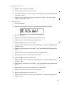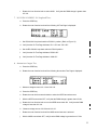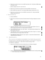
1
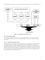
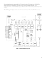
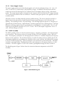
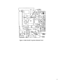
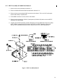
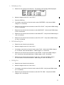
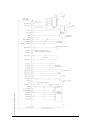
®
GPS 165
Maintenance And Repair
Manual
Garmin International, Inc
1200 E. 151St Street
Olathe, KS 66062
Part Number 190-00066-06
Revision F June, 2003
TABLE OF CONTENTS
SECTION 1
INTRODUCTION
Paragraph
Page
1.1 GENERAL DESCRIPTION ...................................................................................................1
1.2 DETAILED DESCRIPTION ..................................................................................................2
1.2.1 Control/Display Unit (CDU) ......................................................................................2
1.2.2 Main Board Assembly ................................................................................................3
1.2.2.1 Central Processing Unit (CPU) ....................................................................3
1.2.2.2 Power Supply Circuits .................................................................................5
1.2.3 RF/IF Assembly..........................................................................................................5
1.2.4 Interface Board and Data Cards..................................................................................6
1.2.5 Altitude Decoder Board..............................................................................................6
SECTION 2
TROUBLESHOOTING
2.1 TROUBLESHOOTING EQUIPMENT REQUIRED................................................................7
2.2 SELF-TEST FAILURES.........................................................................................................7
2.3 INITIAL TROUBLESHOOTING OPERATIONS ...................................................................8
2.3.1 Power Supply Check..................................................................................................8
2.3.2 Internal Clock Check .................................................................................................8
2.4 Troubleshooting Chart.......................................................................................................10
SECTION 3
DISASSEMBLY INSTRUCTIONS
3.1 REMOVAL OF THE COVERS ............................................................................................12
3.2 BOARD AND MODULE DISASSEMBLY.............................................................................12
3.2.1 Control/Display Unit Removal................................................................................12
3.2.2 Altitude Decoder Board Removal ............................................................................12
3.2.3 Interface Board Removal.........................................................................................13
3.2.4 Main Board Sub-Assembly Removal .......................................................................13
3.2.5 RF/IF Assembly Removal ........................................................................................14
3.2.6 Power/Dimmer Switch Removal .............................................................................15
3.2.7 Rotary Switch Assembly Removal ...........................................................................15
3.2.8 Display Board Removal...........................................................................................15
3.3 REASSEMBLING THE UNIT..............................................................................................16
i
SECTION 4
SERVICE AND TESTING
4.1 MEMORY BATTERY REPLACEMENT................................................................................17
4.2 ROM REPLACEMENT .......................................................................................................18
4.3 FINAL TEST ......................................................................................................................20
4.3.1 Test Equipment Required ........................................................................................20
4.3.2 Set-Up .....................................................................................................................20
4.3.3 Final Test Procedure ................................................................................................20
SECTION 5
ILLUSTRATED PARTS LIST
5.1 LIST OF REPLACEABLE PARTS.......................................................................................31
5.2 SIGNAL & LOAD DIAGRAMS .........................................................................................32
5.3 ASSEMBLY DRAWINGS...................................................................................................34
LIST OF FIGURES
FIGURE 1
FIGURE 2
FIGURE 3
FIGURE 4
FIGURE 5
FIGURE 6
FIGURE 7
FIGURE 8
FIGURE 9
FIGURE 10
FIGURE 11
FIGURE 12
FIGURE 13
FIGURE 14
FIGURE 15
FIGURE 16
GPS 165 BLOCK DIAGRAM..................................................................................2
CONTROL/DISPLAY UNIT BLOCK DIAGRAM.....................................................3
MAIN BOARD BLOCK DIAGRAM.........................................................................4
RF/IF BLOCK DIAGRAM.......................................................................................5
MAIN BOARD TESTPOINTS (TOP VIEW)............................................................8
MAIN BOARD TESTPOINTS (BOTTOM VIEW)....................................................9
RF/IF ASSEMBLY REMOVAL...............................................................................14
ROM TOOL INSERTION ....................................................................................18
ROM REMOVAL .................................................................................................19
J2 REAR CONNECTOR PINOUT DEFINITION ..................................................28
J101 REAR CONNECTOR PINOUT DEFINITION ..............................................29
SIGNAL & LOAD FOR J2 CONNECTOR............................................................32
SIGNAL & LOAD FOR J101 CONNECTOR........................................................33
GPS 165 ASSEMBLY DRAWING 1 ......................................................................34
GPS 165 ASSEMBLY DRAWING 2 ......................................................................35
GPS 165 ASSEMBLY DRAWING 3 ......................................................................36
ii
SECTION 1
INTRODUCTION
This manual is intended to provide instructions and guidelines for the maintenance and repair of the
Garmin GPS 165.
WARNING: This unit contains static sensitive devices. Service personnel must insure that proper precautions
are taken to prevent damage to this equipment from Electro-Static Discharge (ESD). Disassembly and repair
should only be accomplished in an approved ESD workstation by properly trained and grounded personnel.
NOTE: Repair centers operated by Garmin Ltd. or its subsidiaries are authorized to perform component level
repairs to Garmin products. Repair centers operated by Garmin Ltd. or its subsidiaries are authorized to use
Garmin proprietary documentation as references during any component-level repairs performed.
1.1 GENERAL DESCRIPTION
The GPS 165 is a full-featured aviation GPS navigation instrument designed for a fixed panel mounted
installation. The GPS 165 utilizes the patented Garmin MultiTrac™ system for tracking up to eight
satellites simultaneously. The unit features a GPS receiver; a 3-line, 20 character, high-brightness
vacuum fluorescent display, and a front loading NavData® card. The unit is constructed from high
quality materials and uses the latest techniques in manufacturing technology. In order to achieve the
desired reliability, size and power requirements, surface mount components are used extensively.
Specialized equipment and procedures are required to repair circuit boards having surface-mounted
components. Garmin does not authorize the repair of GPS 165 circuit boards. All circuit boards and
assemblies for the GPS 165 can be economically replaced through the Garmin board exchange program,
if necessary.
The following modules and printed circuit board assemblies are field replaceable:
Display Board Assembly:
Contains the vacuum fluorescent display and display circuit board.
Rotary Switch Assembly:
Contains dual concentric switch and its assembled wiring harness.
Control/Display Unit:
Contains bezel, buttons, lens, keypad board, light pipes, front insert, plus the Display Board Assembly
and Rotary Switch Assembly.
Main Board:
Printed circuit board which contains the microprocessor, LSI, power supply circuitry, and battery
charging components.
Altitude Decoder Board:
Printed circuit board which contains the altitude data decoder circuits and interface circuitry.
Interface Board:
Printed circuit board which connects the main board to the NavData® card and the Altitude Decoder
Board.
1
RF/IF Assembly:
Module which contains the GPS receiver and high precision crystal oscillator.
External Battery Pack:
Provides emergency back-up power in case of electrical failure.
1.2
DETAILED DESCRIPTION
Internally, the GPS 165 is divided into six printed circuit boards: the main, RF/IF, altitude decoder,
interface, display, and keypad circuit boards. The block diagram in Figure 1 below shows the
relationships between major circuits and modules within the GPS 165.
Figure 1. GPS 165 Block Diagram
1.2.1 Control/Display Unit (CDU)
The Control/Display Unit is an assembly consisting of ten keycaps, keypad board, optical lens, front
insert panel, vacuum fluorescent display (VFD) and board with drivers, display board shock mounting
grommets and screws. The assembly is housed in a die cast bezel with a dual concentric rotary switch
and two knobs. The VFD is a 3 row by 20 column unit with variable intensity. This display provides
excellent day and night visibility from wide viewing angles. The front panel provides function selection
and alphanumeric input to the Main Board Assembly via 10 push-buttons and the dual concentric rotary
knob. There are two LEDs behind each keycap, providing backlighting for use at night.
2
The block diagram in Figure 2 shows the interaction between components on the Control/Display Unit.
Figure 2. Control/Display Unit Block Diagram
1.2.2 Main Board Assembly
The Main Board Assembly contains the CPU, operating system ROM, system memory, discrete I/O,
serial communication drivers/receivers and the power supply. These items are discussed in further
detail below.
1.2.2.1 Central Processing Unit (CPU)
The Main Board is a microprocessor-based computer board. This board contains an Intel 80L186EB
microprocessor running at 16 MHz, a plug-in read only memory chip (ROM) and random access
memory chips (RAM). Data stored in RAM is maintained by a 3 volt lithium battery when the unit is
switched off, and by the regulated 5 volt supply when the unit is powered on. A custom LSI is used to
decode the signals from the GPS satellites. A real time clock IC is used to keep track of the date and
time. Other circuits on the board are used for input/output functions such as controlling the display,
reading the keypad, and controlling the receiver.
3
Discrete input/output lines are provided for CDI course deviation, CDI to/from flag, CDI NAV flag,
Super Flag, external annunciators, OBS course, and to activate the Approach mode. Serial
communication lines for OBI (clock/data/sync), ARINC 429, RS-422 and RS-232 (two channels) are also
included.
The block diagram in Figure 3 below shows the interaction between the various Main Board circuits.
Figure 3. Main Board Block Diagram
4
1.2.2.2 Power Supply Circuits
The power supply section of the Main Board supplies +60 volts for the display drivers, ±12 volts, +15
volts, +5 volts (VCC), on/off circuits, and the battery charger. In addition, the main board contains
comparator circuits for detecting low Ni-Cad battery level, low memory battery voltage, and external
power. The external power input is through the rear connector (J101) and from the AC adapter through
a DC power jack located near the rear connector. External battery pack power is also applied to the rear
connector (J101).
All of these sources are diode isolated to prevent parallel sourcing. The unit is turned on and off by a
digital latch circuit operated by a knob located on the front panel adjacent to the NavData® card
opening. The switching circuit is a fly-back design. The switching regulator operates at a frequency of
approximately 40 kHz and uses a high efficiency-switching regulator for the switching device. The high
efficiency-switching regulator drives a transformer that is configured in a fly-back mode. The +15 volt
output is post-regulated to provide 11.75 to 12.25 volts. The +5 volt output is regulated at 4.8 to 5.2
volts. All other voltages are ±20%.
1.2.3 RF/IF Assembly
The RF/IF assembly consists of a dual conversion receiver, a frequency synthesizer, and a high precision
crystal oscillator. The receiver consists of a ceramic RF filter, RF and IF amplifiers, mixers, and an IF
filter. The frequency synthesizer uses the high precision oscillator as a reference frequency for the phase
detector in the synthesizer. The resultant frequency is used in the mixer section to produce the first IF.
After further amplification and mixing with a product of the crystal oscillator, the baseband IF is passed
to the CPU Board for processing. The crystal output is also used for the system clock pulse. The RF/IF
assembly is contained within a shielding fence/cover and connection to the antenna is made via a BNC
connector. The RF/IF supplies +5 volts to the antenna’s preamplifier through this BNC connector.
The block diagram in Figure 4 below shows the interaction between components on the RF/IF
Assembly.
Figure 4. RF/IF Block Diagram
5
1.2.4 Interface Board and Data Cards
The Interface Board provides two-way data transfer capability between the Main Board and a data card.
NavData® cards allow for data transfer to the Main Board only. User data cards, with 128 kilobytes of
flash memory data storage, may be used to save user data/settings from the GPS 165 or restore that
information to the GPS 165. Address and data lines from the Main Board route through the Interface
Board’s output buffers to the data card. A plastic race secures the Interface Board at the front of the unit
and serves to guide the data card onto the 40-pin connector.
NOTE: When servicing the GPS 165, user-defined waypoints, routes, settings, etc., may be saved on a
user data card (010-10032-03) first. In the event these data are lost, they may then be restored from the
user data card before the unit is returned to service. Refer to Appendix A of the GPS 165 Pilot’s Guide
for additional information on user data card operation.
1.2.5 Altitude Decoder Board
The Altitude Decoder Board contains the 26-pin rear connector (J2), discrete/parallel inputs and
Gillham/Greycode decoder circuitry. Encoded pressure altitude data from a parallel altimeter device is
received as a 10-bit data word at the 26-pin rear connector. Diode isolation on these input lines
prevents damage to the GPS 165. The data is then decoded and output to the Main Board data bus via
the Interface Board.
The Altitude Decoder Board also provides a discrete input for the GPS SEQ switch. When grounded,
this line activates the GPS 165’s HOLD mode. This input is sent to the Main Board data bus via the
Interface Board.
6
SECTION 2
TROUBLESHOOTING
2.1 TROUBLESHOOTING EQUIPMENT REQUIRED
• 0-30 Volt DC, 3-Amp Power Supply
• Digital Multimeter
• 20 MHz Oscilloscope
2.2 SELF-TEST FAILURES
The GPS 165 monitors many of its internal functions and displays a message to alert the user should a
failure occur. The table below shows the recommended repair for each self-test failure message.
MESSAGE
RECOMMENDED REPAIR
Altitude input fail
Verify connections to altitude serializer/encoder
Replace Altitude Decoder Board (see Section 3.2.2)
Replace Interface Board (see Section 3.2.3)
Replace Main Board (see Section 3.2.4)
Battery requires service
Verify connection of external battery pack to Main
Board
Replace external battery pack
Course input fail
Check ARINC 429 / RS- 422 course input connections
Replace Main Board (see Section 3.2.4)
Data card failed
Replace NavData® card
Replace Interface Board (see Section 3.2.3)
Data card write fail
Replace user data card
Replace Interface Board (see Section 3.2.3)
Fuel/Air input fail
Check connections to fuel/air data system
Replace Main Board (see Section 3.2.4)
Memory battery low
Replace memory battery (see Section 4.1)
No altitude input
Verify connections to altitude serializer/encoder
Replace Altitude Decoder Board (see Section 3.2.2)
Replace Main Board (see Section 3.2.4)
Osc needs adjustment
Replace RF/IF Assembly (see Section 3.2.5)
Replace Main Board (see Section 3.2.4)
RAM failed
Replace Main Board (see Section 3.2.4)
Receiver failed
Replace Main Board (see Section 3.2.4)
Replace RF/IF Assembly (see Section 3.2.5)
ROM failed
Replace ROM (see Section 4.2)
Replace Main Board (see Section 3.2.4)
Stored data lost
Replace memory battery (see Section 4.1)
NOTE: Where multiple repair actions are listed, they are listed with most likely failure cause first.
7
2.3 INITIAL TROUBLESHOOTING OPERATIONS
The first step in troubleshooting the GPS 165 is to remove the top and bottom covers (see Section 3.1).
Verify that the unit is being properly powered and the internal clock is functional. NOTE: Remove the
NavData® card before disassembling the unit.
2.3.1 Power Supply Check
1. Check the DC voltage between D805 and ground as shown in Figure 5. The voltage should be
between -9.60 and -14.40. If the voltage is outside of these limits, replace the Main Board.
2. Check the DC voltage between L800 and ground as shown in Figure 5. The voltage should be
between 4.8 and 5.2. If the voltage is outside of the limits, replace the Main Board.
3. Check the DC voltage between D804 and ground as shown in Figure 5. The voltage should be
between 48.00 and 72.00. If the voltage is outside of these limits, replace the Main Board.
4. Check the DC voltage between I806 pin 1, and ground as shown in Figure 6. The voltage should be
between 11.75 and 12.25. If the voltage is outside of these limits, replace the Main Board.
2.3.2 Internal Clock Check
Check the clock speed by placing an oscilloscope probe at I112 pin 25 as shown in Figure 6. The
frequency should be approximately 16.4 MHz. If the clock is not operational, replace the RF/IF Board.
If the clock still fails to function, replace the Main Board.
Figure 5. Main Board Testpoints (Top View)
8
Figure 6. Main Board Testpoints (Bottom View)
9
2.4
TROUBLESHOOTING CHART
PROBLEM
RECOMMENDED ACTION
Unit will not power on
Check External Power Connection
Check External Battery Pack
Check Pwr/Dimmer Switch Connection
Replace Main Board (see Section 3.2.4)
Replace Pwr/Dimmer Switch (see Section 3.2.6)
Unit will not power off
Replace Main Board (see Section 3.2.4)
Replace Pwr/Dimmer Switch (see Section 3.2.6)
Display has horizontal or vertical lines
Replace Display Board (see Section 3.2.8)
Replace Main Board (see Section 3.2.4)
Display has missing or dark pixels
Replace Display Board (see Section 3.2.8)
Display brightness not adjustable
Replace Pwr/Dimmer Switch (see Section 3.2.6)
Replace Main Board (see Section 3.2.4)
Keycaps have no backlighting
Replace Control/Display Unit (see Section 3.2.1)
Replace Main Board (see Section 3.2.4)
Keycap backlighting not uniform
Replace Control/Display Unit (see Section 3.2.1)
No external annunciator output(s) (message, arrival,
approach)
Check connections and verify operation in Test
Mode (see Section 4.3.3)
Replace Main Board (see Section 3.2.4)
Keycaps do not function properly
Replace Control/Display Unit (see Section 3.2.1)
Replace Main Board (see Section 3.2.4)
Dual concentric (rotary) knobs do not function
properly
Check wiring harness connection from rotary switch
to back of Control/Display
Unit
Replace Rotary Switch Assembly (see Section 3.2.7)
Replace Control/Display Unit (see Section 3.2.1)
Approach select switch not functioning properly
Check connections and verify operation in Test
Mode (see Section 4.3.3)
Replace external switch
Replace Main Board (see Section 3.2.4)
OBS select switch (“course select” or “hold” not
functioning properly)
Check connections and verify operations in Test
Mode (see Section 4.3.3)
Replace external switch
Replace Altitude Decoder Board (see Section 3.2.2)
Replace Main Board (see Section 3.2.4)
GPS reception weak or GPS Status Page shows low
signal levels
Replace Antenna and/or antenna cable
Replace RF/IF Assembly (see Section 3.2.5)
10
TROUBLESHOOTING CHART (Cont.)
PROBLEM
RECOMMENDED ACTION
No GPS reception
Check Date/Time Page for correct UTC time1
Check Position Page for close approximate starting
position (within 300 nautical miles)2
Replace Antenna and/or antenna cable
Replace RF/IF Assembly (see Section 3.2.5)
Replace Main Board (see Section 3.2.4)
Unit displays velocity when not moving3
Replace RF/IF Assembly (see Section 3.2.5)
Ni-Cad battery life is short or Ni-Cad battery inop
Replace External Battery Pack
Replace Main Board (see Section 3.2.4)
Unit loses memory in spite of new memory battery
Replace Main Board (see Section 3.2.4)
Unit does not detect low battery
Replace Main Board (see Section 3.2.4)
Unit does not detect external power4
Check external power communication
Replace Main Board (see Section 3.2.4)
No serial data output
Replace Main Board (see Section 3.2.4)
No external CDI output or external CDI functions
improperly
Check connections and verify operation in Test
Mode (see Section 4.3.3)
Replace Main Board (see Section 3.2.4)
Invalid characters displayed
Replace ROM (see Section 4.2)
Replace Main Board (see Section 3.2.4)
1
If UTC time is incorrect, unit may be reset by holding the CLR key down while turning the unit on. The unit
must then be attached to an antenna, allowed to search the sky and collect new almanac data. This process may
take 20-30 minutes. CAUTION: All user waypoints/settings will be lost if the unit is reset.
2
The GPS 165 will eventually perform an AutoLocate™ and lock onto satellites, however this can add an additional
10-15 minutes to the normal lock-on time.
3
Display of low velocity numbers when not moving can occur when the unit is in 2D mode and should not be
considered a problem. However, this should seldom occur in 3D mode.
4
The “Turning Off” message appears at/below approximately 9 Vdc external power.
11
SECTION 3
DISASSEMBLY INSTRUCTIONS
To avoid damaging the GPS 165’s circuit boards and assemblies, the following procedures should be
carefully followed. Assembly drawings are included in Section 5 for reference (Figures 14 through 16).
3.1 REMOVAL OF THE COVERS
1. Remove the NavData® card.
2. Remove the two M3 x 5mm screws (211-50227-05) retaining the top cover (115-00050-00).
3. Remove the top cover by sliding it rearward approximately 1/4” until the retaining lip is fully exposed.
Thecover can then by lifted off the unit.
4. Carefully turn the unit over. Caution: The GPS 165 contains numerous static-sensitive components.
Always observe proper anti-static precautions.
5. Remove the two M3 x 5mm screws (211-50227-05) retaining the bottom cover (115-00051-00).
6. Remove the bottom cover by sliding it rearward about 1/4” until the retaining lip is fully exposed. The
cover can then be lifted off the unit.
3.2 BOARD AND MODULE DISASSEMBLY
3.2.1 Control/Display Unit (011-00129-00/01) Removal
1. Remove the covers as described above.
2. Remove the power/dimmer control knob and shaft (430-00010-00) by loosening the M3 x 3mm set
screw (211-00037-00) on the coupling sleeve (125-00021-00). NOTE: On some early versions of
the GPS 165, the shaft extension is connected directly to the power/dimmer switch without an in-line
coupler. The control knob is glued to this one piece extension and cannot be removed. If you are
replacing the CDU on one of these units, you will need to order a replacement control knob and
coupling sleeve as well.
3. Remove the four M3 x 5mm flat head screws (211-00024-00) which attach the CDU to the chassis.
4. Carefully remove the CDU from the chassis, pulling the assembly away from the two Main Board
connectors (J100 and J102) and the power/dimmer switch.
3.2.2 Altitude Decoder Board (012-00090-00) Removal
1. Remove the covers as described in Section 3.1.
2. Remove the two #4-40 standoffs (214-00004-00) which hold the 26-pin DSUB connector to the
chassis.
3. Carefully pull the Altitude Decoder Board toward the front of the unit approximately 1/4” until the 26pin DSUB connector is clear of its cutout on the chassis. Lift the Altitude Decoder Board away from
the Main Board and chassis.
4. Remove the ribbon cable connector (J701) from the Altitude Decoder Board.
12
3.2.3 Interface Board (012-00031-01) Removal
1. Remove the covers as described in Section 3.1.
2. Remove the Control/Display Unit as described in Section 3.2.1.
3. Remove the Altitude Decoder Board as described above.
4. Remove the four M1.7 x 5mm flat head screws (211-56201-05) retaining the data card race
(145-00056-00) and Interface Board.
5. Slip the data card race off the Interface Board connector (J700).
6. Carefully pull the Interface Board out of the unit upward, disengaging it from the Main Board
Connector (J107).
3.2.4 Main Board Sub-Assembly (011-00126-xx) Removal
The Main Board Sub-Assembly consists of the CPU Main Board (012-00089-01) and the RF/IF Assembly
(012-00091-00). If required, this sub-assembly may be further disassembled by following the steps in
Section 3.2.5.
1. Remove the covers as described in Section 3.1.
2. Remove the Control/Display Unit as described in Section 3.2.1.
3. Remove the Altitude Decoder Board as described in Section 3.2.2.
4. Remove the hex nut securing the BNC connector to the chassis. This nut is 9/16” and may be
removed with a deep 12-point socket.
5. Pull the BNC connector out of its cutout on the chassis.
6. Remove the heat sink clamping bar (115-00049-00, see Figure 15 - Detail B) by removing the M3 x
5mm mounting screw (211-50227-05).
7. Remove the heat sink insulator (250-00016-00) from regulator I800 (see Figure 15 - Detail B) and
save this piece for later re-assembly.
8. Carefully turn the unit over.
9. The power/dimmer switch uses a flexible circuit cable for connection to the Main Board. This flexible
circuit cable is inserted into a ZIF connector (J804). Pull up on the retaining lip of the ZIF connector.
Gently pull the flexible circuit cable out of the ZIF connector.
10. Remove the two #4-40 standoffs (214-00004-00) which hold the 37-pin DSUB connector to the
chassis.
11. Remove the M3 x 5mm screw (211-50227-05) and the M3 x 8mm screw (211-50207-11) holding the
Main Board to the chassis.
12. Carefully slide the Main Board upward, pulling it away from the power/dimmer switch and the
Interface Board Connector (J702).
13
3.2.5 RF/IF Assembly (012-00091-00) Removal
1. Remove the covers as described in Section 3.1.
2. Remove the Altitude Decoder Board as described in Section 3.2.2.
3. Remove the hex nut securing the BNC connector to the chassis. This nut is 9/16” and may be
removed with a deep 12-point socket.
4. Pull the BNC connector out of its cutout on the chassis.
5. Remove the four screws (211-50202-15) and spacers (233-00012-00) which secure the RF/IF
Assembly to the Main Board.
6. Carefully pull the RF/IF Assembly upward, disengaging it from the Main Board Connector (J803).
NOTE: With the mounting screws removed, the cover for the RF/IF Assembly will be loose.
Grip the RF/IF Assembly firmly by the sides, instead of by its cover, when lifting upward.
Figure 7. RF/IF Assembly Removal
14
3.2.6 Power/Dimmer Switch Removal
1. Remove the covers as described in Section 3.1.
2. Remove the Control/Display Unit as described in Section 3.2.1.
3. Remove the Main Board Sub-Assembly as described in Section 3.2.4.
4. Remove the coupling sleeve (125-00021-00) by unscrewing the pivot pin screw (211-00030-00). (See
Figure 14 on page 34)
5. Remove the hex nut securing the power/dimmer switch to the chassis. This nut is 7/16” and may be
removed with a deep, thin-walled 12-point socket.
6. Slide the power/dimmer switch out of the mounting hole on the chassis.
3.2.7 Rotary Switch Assembly Removal
1. Remove the covers as described in Section 3.1.
2. Remove the Control/Display Unit as described in Section 3.2.1.
3. Remove the two rotary switch knobs by loosening the two M3 x 4mm set screws on the inner knob
(430-00002-01). After removing the inner knob, gently pull the outer knob off of the rotary switch
shaft.
4. Disconnect the rotary switch wiring harness from the connector on the Display Board.
5. Remove the hex nut securing the rotary switch to the Control/Display Unit. This nut is 1/2” and may
be removed with a deep 12-point socket.
3.2.8 Display Board (011-00129-00/01) Removal
1. Remove the covers as described in Section 3.1.
2. Remove the Control/Display Unit as described in Section 3.2.1.
3. Disconnect the rotary switch wiring harness from the connector on the Display Board.
4. Remove the four M2.3 x 6mm screws (211-00028-00) that secure the Display Board to the CDU
bezel.
5. Carefully pull the Display Board away from the CDU bezel, disengaging it from the Keypad Board
connector. Retain the four rubber grommets (252-00005-00) for later assembly.
15
3.3
REASSEMBLING THE UNIT
NOTE: During re-assembly, coat all threaded fasteners with thread-locking compound.
1. Attach the power/dimmer switch to the chassis by reversing the steps followed in Section 3.2.6. The
switch is correctly installed when the contacts and flexible circuit cable are pointing away from the
chassis frame.
2. Ensure that the power/dimmer switch is in the “off” position.
3. Attach the RF/IF Assembly to the Main Board by reversing the steps followed in Section 3.2.5.
4. Mount the Main Board Sub-Assembly on the chassis by reversing the steps followed in Section 3.2.4.
Be sure to pull up on the retaining lip of the ZIF connector (J804) before inserting the flexible circuit
cable. Also, ensure that the heat sink insulator (250-00016-00) is installed on regulator I800 before
installing the heat sink clamping bar (see Figure 15 - Detail B).
5. Mount the Interface Board to the chassis by reversing the steps followed in Section 3.2.3.
6. Install the Altitude Decoder Board by reversing the steps followed in Section 3.2.2. Carefully observe
proper orientation and alignment when reconnecting the ribbon cable to the board.
7. Mount the Display Board to the CDU bezel by reversing the steps followed in Section 3.2.8. Be sure
to reinstall the four rubber grommets before mounting the board.
8. Mount the Rotary Switch Assembly to the Control/Display Unit by reversing the steps followed in
Section 3.2.7. The switch is correctly installed when the wiring harness points toward the top of the
unit. Torque hex nut to 25 ± 3 in oz.
9. Install the Control/Display Unit by reversing the steps followed in Section 3.2.1. Gently slide the CDU
onto the two Main Board connectors (J100 and J102), observing proper pin alignment during the
process.
10. Install the top and bottom covers by reversing the steps followed in Section 3.1.
16
SECTION 4
SERVICE AND TESTING
4.1
MEMORY BATTERY REPLACEMENT
The GPS 165 utilizes a built-in lithium battery to maintain user waypoints/settings stored in RAM. This
battery has an operational life of up to five years. Should the battery require replacements, as indicated
by the “Memory battery low” message, disassembly of the unit will be required to access the battery clip.
When replacing the memory battery, all user waypoints/settings may be lost. If this occurs the message
“Stored Data Lost” will be displayed. The unit must then be attached to an antenna, allowed to search
the sky and collect new almanac data before it will be usable again. This process may take 20-30
minutes. Before beginning replacement of the memory battery, transfer all waypoints and routes to a
user data card so that they may be transferred back to the unit following battery replacement. This
process is covered in the user’s manual.
1. Remove the covers as described in Section 3.1.
2. Remove the Control/Display Unit as described in Section 3.2.1.
3. Remove the four screws (211-50202-15) and spacers (233-00012-00) which secure the RF/IF
Assembly to the Main Board.
4. Carefully pull the RF/IF Assembly upward, disengaging it from the Main Board Connector (J803).
Place the RF/IF Assembly to the side of the unit. NOTE: With the mounting screws removed, the
cover for the RF/IF Assembly will be loose. Grip the RF/IF Assembly firmly by the sides, instead of
by its cover, when lifting upward.
5. Remove the old battery by gently pushing it toward the back of the unit and out of the battery clip. A
tuning tool, or similar flat-tipped instrument, may be used to aid removal of the battery, but
EXTREME CAUTION should be exercised to prevent damage to the Main Board.
6. Immediately install a new battery (positive side up) into the battery clip.
7. Secure the RF/IF Assembly to the Main Board using the four screws (211-50202-15) and spacers
(233-00012-00).
8. Install the Control/Display Unit by reversing the steps followed in Section 3.2.1. Gently slide the CDU
onto the two Main Board connectors (P501 and P502), observing proper pin alignment during the
process.
9. Turn the GPS 165 on and press ENT to accept “NORMAL” mode operation. Press ENT again to
accept the Database Page.
10. Verify that the “Memory battery low” message does not appear on the Message Page by pressing the
MSG key.
11. Turn the GPS 165 off and carefully turn the unit over.
12. Verify that the memory battery voltage (from test point to ground, see Figure 6) is at least 2.9 Vdc.
13. Install the top and bottom covers by reversing the steps followed in Section 3.1.
17
4.2
ROM REPLACEMENT
If a software update is required, it may be performed by replacing the operating system ROM located on
the Main Board. When replacing the ROM, all user waypoints/settings will be lost. The message “Stored
Data Lost” will be displayed. The unit must then be attached to an antenna, allowed to search the sky
and collect new almanac data before it will be usable again. This process may take 20-30 minutes. (A
user data card is available to save use waypoints/settings prior to replacing the ROM.) Refer to page 9 of
this manual for more information.
1. Turn the GPS 165 off.
2. Remove the bottom cover as described in Section 3.1.
3. Locate the ROM in the middle of the Main Board as shown in Figure 6.
NOTE: The ROM removal tool is contoured for insertion into either of the two extraction cavities on the
chip carrier socket. Remove the chip by inserting the extraction tool with the correct angle (see Figure
8), and pivoting the tool on its heel against the socket.
Figure 8. ROM Tool Insertion
4. ROM Extraction Procedure:
a. Orient the socket and tool as shown in Figure 9.
CAUTION: Do not attempt to completely extract chip from chip carrier socket on the first extraction.
Lift from one side until the corner is above the socket, then repeat the procedure on the opposite corner.
18
Figure 9. ROM Removal
b. Insert the extraction tool into the socket so that the front angle of the tool is perpendicular to
the chip carrier. NOTE: Insertion of the tool with an incorrect angle will result in damage to the
chip carrier socket. The incorrect angle will bottom under the standoff rather than the bottom
of the chip.
c. Lower the extraction tool into the extraction cavity until it bottoms.
d. Using a slight downward pressure, rotate the tool away from the chip carrier until the corner of
the chip lifts away from the chip carrier socket.
e. Repeat on opposite extraction slot and lift chip out of chip carrier socket.
5. Inspect the ROM socket to ensure that the contacts and case are in good condition.
6. Insert the new ROM into the socket so that the beveled corned of the ROM chip aligns with the
beveled corner of the socket (see Figure 6). Make certain that the ROM is well seated!
7. Hold the CLR key down while rotation the power/dimmer knob clockwise from the ‘off’ position. Verify
that the Self-Test Page is displayed (shows the software version number and copyright notice). Also,
press the MSG key to verify that the “Stored data lost” message appears on the Message Page and
the “ROM failed” message does not appear. (Failure to clear memory after ROM replacement can
cause unpredictable operating problems.)
8. Turn the GPS 165 off.
9. Install the bottom cover by reversing the steps followed in Section 3.1.
10. Connect an outside antenna to the GPS 165, turn the unit on and allow it to recollect almanac data as
described above. This process is complete when the “Collecting Data” message is no longer
displayed on the Message Page.
19
4.3 FINAL TEST
After completing all necessary maintenance or service, the following test procedure is provided to ensure
that all GPS 165 functions are operating properly.
4.3.1 Test Equipment Recommended
The following standard equipment (or suitable substitutes) is needed to perform testing:
•
•
•
•
•
•
•
0-30 Volt DC/ 3 amp Power Supply
Digital Multimeter
BF Goodrich Precision Track Selector
GPS Antenna- Garmin GA 56 (P/N 010-10040-01)
Male to Male BNC cable giving 10 ± 1 dB attenuation (P/N 320-00088-00)
Red and Black Cables with Bananna Plugs (3 ft. recommended)
60 MHz Oscilloscope
NOTE: Test Fixtures/Test Harnesses are User Supplied. Signal & Load information given in Figures 12
and 13 can aid in the fabrication of any Test Fixtures or Panels.
4.3.2 Setup
1. Before connecting a test harness to the unit, set the power supply to +13.8 Vdc ±.01 V at pin
J101-25. Set the current limiter to 3 A.
2. Turn the power supply OFF.
3. Connect a test harness (see Signal & Load diagrams on pages 32, 33) to the unit and turn the
power supply ON.
4.3.3 Final Test Procedure
1. Test Mode Activation/Display Test:
a.
Hold the ENT key down while rotating the power/dimmer knob clockwise from the `off’
position.
b.
Verify that the GPS 165 enters test mode. There are three test patterns displayed when first
activating test mode. The first test pattern illuminates all thirty-five pixels in the first character
column of each row and cycles through the remaining nineteen character columns. The
second test pattern illuminates the first column of pixels in each of the 20 character columns
and cycles through the remaining four pixel columns. The third test pattern illuminates the
first row of pixels in each of the three character rows and cycles through the remaining six
pixel rows.
c.
Observe the test patterns and verify that the display is working properly.
d.
Rotate the power/dimmer knob counterclockwise, but not past the detent (off) position, to
ensure that the display is dimmable.
20
2. CDI Deflection Test:
a.
Rotate the outer function knob clockwise. The following CDI Test Page will be displayed:
b.
Measure voltage across J101-1 and J101-4.
c.
Press the CRSR key.
d.
If necessary, rotate the inner function knob to select CENTERED. Verify that the DMM
voltage is 0 ± 15 millivolts.
e.
Rotate the inner function knob clockwise to select FULL RIGHT. Verify that the DMM voltage
is -150 ± 15 millivolts.
f.
Rotate the inner function knob clockwise to select MAX RIGHT. Verify that the DMM voltage
is -300 ± 30 millivolts.
g.
Rotate the inner function knob clockwise to select MAX LEFT. Verify that the DMM voltage is
+300 ± 30 millivolts.
h.
Rotate the inner function knob clockwise to select FULL LEFT. Verify that the DMM voltage
is +150 ± 15 millivolts.
3. CDI To/From Flag Test:
a.
Rotate the outer function knob clockwise.
b.
Measure voltage across J101-2 and J101-4.
c.
If necessary, rotate the inner function knob to select FLAG. Verify that the DMM voltage is
0 ± 15 millivolts. Units with Mod Status 1: DMM voltage is 0 ± 10 millivolts.
d.
Rotate the inner function knob clockwise to select FROM. Verify that the DMM voltage is
-83 ± 20 millivolts. Units with Mod Status 1: DMM voltage is -190 ± 40 millivolts.
e.
Rotate the inner function knob clockwise to select TO. Verify that the DMM voltage is
83 ± 20 millivolts. Units with Mod Status 1: DMM voltage is +190 ± 40 millivolts.
4. CDI Flag Test:
a.
Rotate the outer function knob clockwise.
b.
Measure voltage across J101-3 and J101-4.
c.
If necessary, rotate the inner function knob to select IN VIEW. Verify that the DMM voltage
is 0 ± 10 millivolts.
d.
Rotate the inner function knob clockwise to select OUT OF VIEW. Verify that the DMM
voltage is 375 ± 80 millivolts.
21
5. Super Flag Output Test:
a.
Rotate the outer function knob clockwise.
b.
Measure voltage across J101-10 and J101-26.
c.
If necessary, rotate the inner function knob to select IN VIEW. Verify that the DMM voltage
is less than 0.25 Vdc.
d.
Rotate the inner function knob clockwise to select OUT OF VIEW. Verify that the DMM
voltage is greater than 12.8 Vdc.
6. OBI Output Test:
a. Press the CRSR key.
b. Rotate the outer function knob clockwise to display the following OBI Test Page:
c.
Press the CRSR key.
d. Rotate the outer function knob clockwise until VALUE is flashing.
e. Rotate the inner function knob clockwise to select CLOCK.
f.
Measure voltage across J101-7 and J101-26.
g. Rotate the outer function knob clockwise until LOW flashes. Verify that the DMM voltage is
less than 1.0 Vdc.
h. Rotate the inner function knob to select HIGH. Verify that the DMM voltage is greater than
4.5 Vdc.
i.
Rotate the outer function knob counterclockwise until CLOCK flashes.
j.
Rotate the inner function knob clockwise to select DATA.
k.
Measure voltage across J101-8 and J101-26.
l.
Rotate the outer function knob clockwise until LOW flashes. Verify that the DMM voltage is
less than 1.0 Vdc.
m. Rotate the inner function knob to select HIGH. Verify that the DMM voltage is greater than
4.5 Vdc.
n. Rotate the outer function knob counterclockwise until DATA flashes.
o. Rotate the inner function knob clockwise to select SYNC.
p. Measure voltage across J101-23 and J101-26.
q. Rotate the outer function knob clockwise until LOW flashes. Verify that the DMM voltage is
less than 1.0 Vdc.
22
r.
Rotate the inner function knob to select HIGH. Verify that the DMM voltage is greater than
4.5 Vdc.
7. RS-232/RS-422/ARINC 429 Loopback Tests:
a. Press the CRSR key.
b. Rotate the outer function knob until the following I/O Test Page is displayed:
c.
Set RS-232/422 Loop-back switch to RS232-1 position. (Refer to Figure 13)
d. Verify that the I/O Test Page indicates “CH 1 OK” and “CH 2 OK”.
e. Set the RS-232/422 Loop-back switch to RS 422 position.
f.
Verify that the I/O Test Page indicates “RS422 OK”.
g.
Verify that the I/O Test Page indicates “A429 OK”.
8. Annunciator Output Test:
a. Press the CRSR key.
b. Rotate the outer function knob until the following Annunciator Test Page is displayed:
c.
Measure voltage across J101-13 and J101-26.
d. Press the CRSR key.
e. Rotate the outer knob counterclockwise to select the APPR annunciator test.
f.
With the APPR annunciator OFF, verify that the DMM voltage is greater that 4.5 Vdc.
g. Rotate the inner function knob to turn the APPR annunciator ON. Verify that the DMM
voltage is less than 0.3 Vdc.
h.
Measure voltage across J101-20 and J101-26.
i.
Rotate the outer function knob until the MSG annunciator test is selected.
j.
With the MSG annunciator OFF, verify that the DMM voltage is greater than 4.5 Vdc.
23
k.
Rotate the inner function knob to turn the MSG annunciator ON. Verify that the DMM voltage
is less than 0.3 Vdc.
l.
Measure voltage across J101-12 and J101-26.
m. Rotate the outer function knob clockwise to select the ARRVL annunciator test.
n. With the ARRVL annunciator OFF, verify that the DMM voltage is greater than 4.5 Vdc.
o. Rotate the inner function knob to turn the ARRVL annunciator ON. Verify that the DMM
voltage is less than 0.3 Vdc.
9. External Switches Test:
a. Press the CRSR key.
b. Rotate the outer function knob until the External Switches Test Page is displayed, as shown
below.
c.
Toggle the APPR SELECT switch (J101-9) to the ‘grounded’ position (Refer to Figure 13).
Verify that the External Switches Test Page indicates “APPR ON”.
d. Toggle APPR SELECT switch to the ‘open’ position. Verify that the External Switches Test
Page indicates “APPR OFF”.
e. Toggle OBS HOLD switch (J2-13) to the ‘grounded’ position. (Refer to Figure 12) Verify that
the External Switches Test Page indicates “HOLD ON”.
f.
10.
Toggle OBS HOLD switch (J2-13) to the ‘open’ position. Verify that the External Switches
Test Page indicates “HOLD OFF”.
Altitude Decoder Test:
This test exercises each altitude data line individually. Most altitude codes presented will
be invalid, however, ALTITUDE DECODER LINE SELECT switch positions C1 (input line
C1 valid) and C2 (input line C2 valid) indicate altitude readings of -800
and -1000 feet, respectively.
a.
Rotate the outer function knob until the Altitude Decoder Test Page is displayed:
b.
Close the switch for input line D4. Verify that D4 on the Altitude Decoder Test Page indicates
“1”. All other altitude inputs should indicate “0”.
24
c.
11.
12.
Continue to step through input lines A1, A2, A4, B1, B2, B4, C1, C2, and C4. Verify that only
one input line (A1, A2, A4, B1, B2, B4, C1, C2, or C4) indicates “1” for each switch position.
All other altitude inputs should still indicate “0”.
OBS Selected Course Test:
a.
Rotate the outer function knob until the OBS Selected Course Test Page is displayed:
b.
Attach OBS Signals to respective pins on Precision Track Selector. Set Track Selector to
150°. Verify that the input course is 150° ± 9° and “CALIB?” appears in the lower right corner
of the test page.
c.
Press the CRSR key.
d.
Press the ENT key on the GPS 165 to calibrate the unit. There will be a brief delay while the
unit performs the calibration. Verify that the input course is now 150° ± 0.2°.
e.
Set the Track Selector to the 60°, 240°, and 330° positions. Verify that in each instance the
input course is within ± 2°.
External Power/Battery Tests:
a.
Rotate the outer function knob until the Battery Test Page is displayed:
b.
Verify that line two of the display indicates “External Power” and the voltage reading is
approximately 13.8 ±0.3 Vdc.
c.
Connect the wall charger to the unit and verify that line two of the display now indicates
“Charger-Trickle Chrg”.
d.
Unplug the wall adapter. Line two of the display should go back to indicating ‘External
Power’.
e.
Verify that line 2 of the display indicates “Rmt Pak none”.
f.
Verify that line 3 of the display indicates “Mem Bat ok”.
25
13.
GPS Receiver Noise Test:
a. Rotate the outer function knob until the GPS receiver test page is displayed:
b. Terminate the GPS receiver’s antenna connection into a 50 ohm load.
c.
14.
The bottom line of the display represents the receiver noise level. Verify that this number is
within the range of 1800 and 2200.
Operational Test:
a.
Turn the GPS 165 OFF.
b.
Insert a Jeppesen NavData® card.
c.
Turn the GPS 165 ON normally, without entering the test mode. Verify that the GPS 165
passes its self-test. A failure is indicated by one of the messages listed in Section 2.2.
d.
Verify that the GPS 165 correctly reads the NavData® card and indicates the type, effective
date and expiration date.
e.
Press the ENT key and verify that the Satellite Status Page is displayed.
f.
Press the MSG key and verify that the Message Page is displayed.
g.
Press the Direct To key and verify that the GO TO Page is displayed.
h.
Rotate the inner function knob to select a letter or number on the display.
i.
Press the CLR key and verify that the selected letter/number disappears.
j.
Press the NRST key. Verify that a Nearest Waypoint Page is displayed.
k.
Press the SET key. Verify that a Set-Up Page (Satellite Status Page) is displayed.
l.
Press the RTE key. Verify that a Route Page is displayed.
m.
Press the WPT key. Verify that the Select Waypoint Type Page is displayed.
n.
Press the CRSR key and verify that APT? flashes.
o.
Rotate the outer function knob clockwise and verify that VOR? flashes.
p.
Press the NAV key. Verify that a Navigation Page is displayed.
q.
Turn the GPS 165 OFF.
26
15.
Satellite Tracking Test:
The Satellite Tracking Test ensures that the GPS 165 has current almanac information
and is able to lock onto a sufficient number of satellites to provide a position. This test
also verifies that the signal strength of the satellites received is at an acceptable level.
a.
Turn the unit off.
b.
Connect unit to a GA56 antenna mounted outside with a clear view of the sky, through a coax
with a 10dB ± 1dB cable loss @ 1.5 GHZ. Note: attenuation pads must not be used since the
unit supplies the GA56 with DC power.
c.
Turn on the unit. Go to the satellite Data Page (see Pilot’s Guide for instructions).
d.
Allow the unit to lock on to the satellites.
e.
Then unit must enter 3D navigation mode
f.
The unit must display the following:
1. Four satellites with signal strength greater than 3.
2. The average signal strength of 3.5 on satellites above 20º elevation.
27
PIN #
DESCRIPTION
13
SEQUENCE HOLD LOW(OBS)
14
ALTITUDE D4
15
ALTITUDE A1
16
ALTITUDE A2
17
ALTITUDE A4
18
ALTITUDE B1
19
ALTITUDE B2
20
ALTITUDE B4
21
ALTITUDE C1
22
ALTITUDE C2
23
ALTITUDE C4
24
ALTITUDE COMMON
Figure 10. J2 Rear Connector Pin-Out Definition
28
PIN #
DESCRIPTION
1
GPS D-BAR LEFT +
2
GPS TO +
3
GPS FLAG +
4
GPS FLAG -
5
GPS D-BAR RIGHT +
6
GPS FROM +
7
GPS OBI CLOCK
8
GPS OBI DATA
9
APPROACH ARM LOW
10
GPS SUPERFLAG HIGH
11
RS-422 IN HI
12
ARRIVAL ANNUNCIATE LOW
13
APPRCH ANNUNCIATE LOW
14
GPS ROTOR C
15
ARINC 429 OUT B
16
ARINC 429 OUT A
17
RS-232 IN 1
18
RS-232 IN 2
19
RS-232 OUT 2
20
MESSAGE ANNUNCIATE LOW
21
RESERVED
22
RESERVED
23
GPS OBI SYNC
24
RS-232 OUT 1
25
AIRCRAFT POWER (10-33 Vdc)
26
GROUND
27
RS-422 IN LO
28
RESERVED
29
RESERVED
30
REMOTE BATTERY, +
31
REMOTE BATTERY, TEMP
32
ARINC 429 IN A
29
PIN # (cont.)
DESCRIPTION (cont.)
33
ARINC 429 IN B
34
REMOTE BATTERY
35
GPS STATOR D
36
RESERVED
37
GPS STATOR F
Figure 11. J101 Rear Connector Pin-Out Definition
30
SECTION 5
ILLUSTRATED PARTS LIST
5.1 LIST OF REPLACEABLE PARTS
The table below lists the parts that are available to authorized maintenance shops.
Part Number
Description
011-00129-00
CDU Assy – GPS 165
011-00129-01
CDU Assy – GPS 165, Grey
011-00137-00
Keypad, GPS 165
011- CS030-00
Use 012-00091-00
011-CS032-00
Pwr/Dim Sw w/ flex ckt. Cble
011-CS032-01
Rtry Swch Assy w/ wire Hrns
012-00029-00
Display Board Assy
012-00031-01
Interface Assy
012-00089-01
CPU Bd Assy
012-00090-00
Altitude Decoder Bd
012-00091-00
TSO’d RF/IF Assy w/ BNC Conn
115-00050-00
Top Cover, Dzus Mount
115-00051-00
Bottom Cover, Dzus Mount
360-00003-01
Lithium Cell, 2023
430-00002-01
Knob, Inner, w/o Trim Ring
430-00006-00
Knob, Outer
430-00010-00
Knob, Power/Dimmer
470-00006-00
Lens –GPS 165
541-B0034-00
Programmed EPROM
NOTE
The drawings in this section are for reference only. Part numbers listed on drawings are
for identification purposes and cannot be supplied by Garmin. Only the parts mentioned
in Section 5.1 are still supplied by Garmin.
31
5.2 Signal & Load Diagrams
Figure 12 Signal & Load for J2 Connector
32
Figure 13 Signal & Load for J101 Connector
33
5.3 Assembly Drawings
Figure 14. GPS 165 Assembly Drawing 1
34
Figure 15. GPS 165 Assembly Drawing 2
35
Figure 16. GPS 165 Assembly Drawing 3
36