1
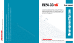
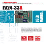
SOFTWARE AND HARDWARE SOLUTIONS FOR THE EMBEDDED WORLD
LV 24-33
User’s Manual
MikroElektronika
Development tools - Books - Compilers
mikro
3 in 1
USB 2.0
DEBUGGER
IN-CIRCUIT
ICD
IN-CIRCUIT
PROGRAMMER
MICROCHIP
24/33
DEVELOPMENT
BOARD
With useful implemented peripherals, plentiful practical
code examples and a broad set of additional add-on
boards (Serial Ethernet, Compact Flash, MMC/SD,
ADC, DAC, CAN, RTC, RS-485, etc.), MikroElektronika
development boards make fast and reliable tools that
can satisfy the needs of experienced engineers and
beginners alike.
Software and Hardware
solutions for Embedded World
LV 24-33
KEY FEATURES
1. External power supply from 8 to 16 V
AC/DC.
2. Choose between external and USB
power supply. When powering from your
PC’s USB port, you don’t need an external supply.
3. Very fast and flexible USB programmer
on board. The key feature is expandability. By downloading new software, you will
be able to program new MCUs in coming
years.
4. DS1820 temperature sensor allows you
to measure temperature with 0.5°C accuracy.
5. Two RS232 communication ports RS232-A and RS232-B.
6. For presentation purposes, all PORTB
pins are connected to, and can be
used for measuring voltages set by, the
potentiometers P1, P2, P3 and P4.
7. MMC/SD slot for multimedia cards with up to 2GB storage space.
8. Setting the jumper to the upper position sets the pins of the
appropriate port to logical one (pull-up). If the jumper is set to the
lower postion, pins are set to logical zero (pull-down). It is very
important to select pull-up for a port if you expect logical zero on
its inputs and vice versa.
9. You can connect an LCD if you need it for your application in
4-bit mode.
10. You can connect a Graphic LCD if you need it for your application
or LCD in 8-bit mode.
11. LV 24-33 supports 80-pin and 100-pin PIC24 and dsPIC33
microcontrollers.
12. 85 buttons allow you to control every pin on your microcontroller.
13. You can choose how pressing the button will affect the pin, high
state or low state.
14. See all the signals - each pin has an LED.
15. Set LCD contrast according to your display characteristics.
16. All switches on SW2 and SW3 turns ON or OFF the LEDs on all
PIC24 or dsPIC33 ports. You can choose which port you want
LEDs to be connected to. In certain applications, it is important to
remove all unnecessary connections from pins. These DIP
switches let you disconnect all LEDs from MCU pins.
17. On-Board peripherals are connected to the microcontroller using
SW1. MMC/SD Card is connected to the microcontroller through
the switches 5, 6, 7 and 8. Both RS232 communication ports are
connected to MCU using first four switches on SW1.
18. PORTB is connected to a resistor network, using switches SW4
and SW5. If a switch is in OFF position, the appropriate pin has
either pull-up or pull-down resistor attached. This is very
important as it enables PORTB to be used in analog mode as
an A/D converter as well as an ordinary digital I/O port.
19. ICD2 (In-Circuit Debugger) connector.
20. Reset circuit - if the reset button is pressed a hardware reset will
take place (MCU will start executing from the beginning).
CONTENTS
LV 24-33 User’s Manual
MikroElektronika
Development tools
CONTENTS
LV 24-33
with USB 2.0 PROGRAMMER
CONNECTING THE SYSTEM
page 4
INTRODUCTION
page 5
DESCRIPTION OF THE DEVELOPMENT SYSTEM
page 6
Switches and their functions
page 6
Jumpers
page 7
MCU sockets
page 8
Power Supply
page 11
On-Board USB 2.0 programmer
page 12
LEDs
page 13
Pushbutton switches
page 15
Graphic LCD
page 18
LCD 2x16 in 4-bit mode
page 20
LCD 2x16 in 8-bit mode
page 21
RS-232 Communication
page 23
DS1820 Digital Thermometer
page 26
A/D Converter input
page 27
Direct port access
page 29
ICD2 (In-Circuit Debugger) connector
page 31
MMC/SD (Multimedia Card)
page 32
page
MIKROELEKTRONIKA SOFTWARE AND HARDWARE SOLUTIONS FOR THE EMBEDDED WORLD
3
CONNECTING THE SYSTEM
LV 24-33 User’s Manual
MikroElektronika
Development tools
CONNECTING THE SYSTEM
The development system box contains the development system, product CD, USB cable,
RS232 cable and this manual.
Step no.1 The first thing to do is to take the system out of the box. Unpack the USB cable and connect
it to the PC. Please use USB ports on the back of the PC with direct connection to the motherboard.
Step no.2 Install the LvPICFlash programmer and drivers. Start the installation from the product CD:
CD_Drive:/product/zip/LvPICFlash_setup.exe.
Step no.3 After the installation connect the USB cable to the LV 24-33 board. You will be asked for
the LvPICFlash drivers. Point to them in order to finish the driver installation. They are
placed in folder:
System_Drive:\Program Files\Mikroelektronika\LVPICFLASH\Driver.NT
Step no.4 Run and use LvPICFlash as it is explained in the PDF document ‘LvPICFlash programmer’:
CD_Drive:/product/pdf/lvpicflash_manual.pdf
After these 4 steps, your LV 24-33 is installed and ready for use. You can try to read a program from the chip or to load an example from the examples folder of mikroElektronika’s
compilers for dsPIC or from the product CD:
CD_Drive:/product/zip/lv24_33_examples.zip.
page
4
MIKROELEKTRONIKA SOFTWARE AND HARDWARE SOLUTIONS FOR THE EMBEDDED WORLD
LV 24-33
with USB 2.0 PROGRAMMER
MICROCHIP
24/33
DEVELOPMENT
BOARD
INTRODUCTION
The LV 24-33 development system is a full-featured development board for Microchip
PIC24 and dsPIC33 microcontrollers. It has been designed to allow students and engineers
to easily exercise and explore the capabilities of PIC24 and dsPIC33 microcontrollers. It
allows PIC24 and dsPIC33 microcontrollers to be interfaced with external circuits and a
broad range of peripheral devices, allowing a user to concentrate on software development.
Figure 1 illustrates the development board. Each component is marked on a silkscreen, both
top and bottom. These marks describe connections to the microcontroller, operation modes,
and provide some useful notes. The need for additional schematics is minimized since all
relevant information is printed on the board.
Figure 1.
LV 24-33
with USB 2.0 PROGRAMMER
LV 24-33 development board
page
MIKROELEKTRONIKA SOFTWARE AND HARDWARE SOLUTIONS FOR THE EMBEDDED WORLD
5
INTRODUCTION
LV 24-33 User’s Manual
MikroElektronika
Development tools
SWITCHES
LV 24-33 User’s Manual
MikroElektronika
Development tools
SWITCHES
The LV 24-33 development board features a number of peripherial devices. In order to
enable these devices before programming, you need to check if appropriate jumpers or
switches have been properly set. Switches are devices that have two positions - ON and
OFF, which have a role to establish or break a connection between two contacts. The
LV 24-33 development board has four groups of switches.
The switches on SW1 are used to enable connection between the microcontroller pins and
both RS232 communication devices. The first two switches are used for RS232 A
communication lines, while the second two are used for RS232 B communication lines.
Switch SW1 is also used to enable SPI communication and to enable connection between
the microcontroller pin and CS pin for MMC/SD Card.
The switches on SW2 and SW3 are used to enable LEDs connected to PORTA, PORTB,
PORTC, PORTD, PORTE, PORTF and PORTG.
The switches on SW4 and SW5 are used to enable a connection between the microcontroller PORTB with external pull-up/down resistors. When PORTB pins are used as digital
inputs/outputs, the appropriate pull-up/down resistors should be enabled.
ON
Group of 8 switches
1 2 3 4 5 6 7 8
Figure 2.
Switches 1 and 2 are ON,
and other switches are OFF
Switch is ON
Switch is OFF
page
6
MIKROELEKTRONIKA SOFTWARE AND HARDWARE SOLUTIONS FOR THE EMBEDDED WORLD
LV 24-33
with USB 2.0 PROGRAMMER
JUMPERS
Jumpers, like switches, can break or establish a connection between two points. Beneath the
plastic cover of the jumper is a metal contact, which makes a connection when the jumper
is placed between two disconnected pins.
For example, the jumpers group J8 is used to connect or disconnect potentiometer P4 to
RB12, RB13, RB14 or RB15 line. A connection is made when the jumper is placed between
two contacts.
Figure 3.
Jumper as a
switch
Jumper is ON
Jumper is OFF
More often, jumpers are used as a selector between two possible connections using a three
pin connector. As illustrated in Fig. 4, the middle connector can be connected to the left or
right pin, depending on the jumper’s position.
Figure 4.
All lines are
disconnected
Left line
is selected
Right line
is selected
Jumper as a
multiplexer
LV 24-33
with USB 2.0 PROGRAMMER
page
MIKROELEKTRONIKA SOFTWARE AND HARDWARE SOLUTIONS FOR THE EMBEDDED WORLD
7
JUMPERS
LV 24-33 User’s Manual
MikroElektronika
Development tools
MCU CARD
LV 24-33 User’s Manual
MikroElektronika
Development tools
MCU CARD
The LV 24-33 development board has a 104-pin MCU Card. If you want to use some other
microcontroller, all you have to do is to change MCU Cards. You can use 80-pin MCUs
(PIC24FJ128GA008 for example) or 100-pin MCUs (dsPIC33FJ256GP710 for example).
LV 24-33 MCU Card is shown on the following picture:
MCU Card
Figure 5.
page
8
MIKROELEKTRONIKA SOFTWARE AND HARDWARE SOLUTIONS FOR THE EMBEDDED WORLD
LV 24-33
with USB 2.0 PROGRAMMER
When you are placing MCU Card on the LV 24-33 MCU socket, you must follow these
steps:
Step no.1
If there is already MCU Card
placed on LV 24-33, you must
remove it by slowly pulling it up.
Step no.2
Place MCU Card on the board.
Note that label on the MCU Card
must be at the upper-left corner as
it is drawn on the LV 24-33 board.
Step no.3
When MCU Card is on the place,
push it down by applying the
pressure on all edges at the same
time.
LV 24-33
with USB 2.0 PROGRAMMER
page
MIKROELEKTRONIKA SOFTWARE AND HARDWARE SOLUTIONS FOR THE EMBEDDED WORLD
9
MCU CARD
LV 24-33 User’s Manual
MikroElektronika
Development tools
LV 24-33 User’s Manual
MikroElektronika
Development tools
MCU CARD
Microcontroller’s pins are routed to various peripherals as illustrated in Fig. 6. All ports have
direct connections to Direct Port Access connectors. Such connectors are typically used for
connecting external peripherals to the board or for providing useful points for connecting
digital logic probe.
All ports are connected to LEDs, push-button switches and pull-up/down resistors, which
allow easy monitoring and testing of digital pin state .
Some pins are connected to other peripherials such as the DS1820 temperature sensor,
RS-232 communication, LCD, etc.
SW3
PORTE low
RE7
ON
PORTE_L
1 2 3 4 5 6 7 8
CN22
VCC3.3
VCC3.3
J1
J22
PORTE low
VCC3.3
VCC3.3
RE7
10uF
RE4
RE3
RE2
RG13
RG12
RG14
RE1
RE0
RA7
RA6
RG0
RG1
FR1
RF0
ENVREG
VDDcore
RD7
RD6
RD5
RD4
RD13
RD12
RD3
RD2
RD1
RE7
System connection
PIC24FJ96GA010
dsPIC33FJ128MC710
VSS
RC14
RC13
RD0
RD11
RD10
RD9
RD8
RA15
RA14
VSS
OSC2
OSC1
VDD
RA5
RA4
RA3
RA2
RG2
RG3
RF6
RF7
RF8
RF2
RF3
X1
10MHz
C1
22pF
C2
22pF
RB6
RB7
RA9
RA10
AVDD
AVSS
RB8
RB9
RB10
RB11
VSS
VDD
RA1
RF13
RF12
RB12
RB13
RB14
RB15
VSS
VDD
RD14
RD15
RF4
RF5
Figure 6.
100n
Reset
10K
VCC3.3
RG15
VDD
RE5
RE6
RE7
RC1
RC2
RC3
RC4
RG6
RG7
RG8
MCLR
RG9
VSS
VDD
RA0
RE8
RE9
RB5
RB4
RB3
RB2
RB1
RB0
VCC3.3
page
10
MIKROELEKTRONIKA SOFTWARE AND HARDWARE SOLUTIONS FOR THE EMBEDDED WORLD
LV 24-33
with USB 2.0 PROGRAMMER
POWER SUPPLY
SELECTABLE
POWER SUPPLY
As a power supply source, users can select either a regulated supply from the USB cable
(default) or an external power supply. In case of the USB power supply, the system should
be connected to a PC using the USB programming cable, while the jumper J4 should be set
in the right-hand position.
In the case of an external power supply, the LV 24-33 board produces +5V using an LM7805
voltage regulator. The external power supply can be AC or DC, with a voltage between 8V
and 16V and the jumper J4 should be set in the left-hand position. In Fig. 7 you can see
USB and external power supply connectors. There is also 3.3V voltage regulator
(MC33269DT-3.3) for 3.3V power supply.
Figure 8. Power supply select jumper
Figure 7. USB and power supply connectors
J4 in the left-hand
position: system will
take power from the
external AC/DC
power adapter.
J4 in the right-hand
position: system will
take power from the
USB cable.
USB
connector
External power
supply connector
EXT
USB
USB Power Supply
EXT
USB
External Power Supply
REG4
7805
CN11
1
8-16V (AC/DC)
+
1
Vin
Vout
J4
5V
FP1
5V
3
GND
VCC
2
2
E17
470uF
C15
100nF
C14
100nF
E18
470uF
C6
100nF
VCC
DD+
GND
USB
REG1
MC33269DT-3.3
VCC3.3
Figure 9.
Power supply schematic
LV 24-33
with USB 2.0 PROGRAMMER
Vout
2
Vin
GND
3
1
E1
10uF
C1
100nF
page
MIKROELEKTRONIKA SOFTWARE AND HARDWARE SOLUTIONS FOR THE EMBEDDED WORLD
11
POWER SUPPLY
LV 24-33 User’s Manual
MikroElektronika
Development tools
USB 2.0
IN-CIRCUIT
PROGRAMMER
MikroElektronika
Development tools
ON-BOARD USB 2.0 PROGRAMMER
There is no need for the use of external
equipment during programming, as the
LV 24-33 development system has its own
on-board USB 2.0 programmer.
All you need to do is connect the system to
a PC using the USB cable. Then, load your
program into the microcontroller via the
LvPICFlash programming software, which
is supplied with the board.
Figure 10. On-Board USB programmer
Note: There is no need for manually reseting MCU after programming. The programmer
will reset the MCU automatically.
VCC3.3
VCC
10uF
VCC
USB LINK
VCC
1K
10K
SWITCH
Reset
U1
100n
PIC24FJ96GA010
dsPIC33FJ128MC710
VSS
RC14
RC13
RD0
RD11
RD10
RD9
RD8
RA15
RA14
VSS
OSC2
OSC1
VDD
RA5
RA4
RA3
RA2
RG2
RG3
RF6
RF7
RF8
RF2
RF3
X1
10MHz
C1
22pF
LvPICflash
On-Board USB
programmer
RG15
VDD
RE5
RE6
RE7
RC1
RC2
RC3
RC4
RG6
RG7
RG8
MCLR
RG9
VSS
VDD
RA0
RE8
RE9
RB5
RB4
RB3
RB2
RB1
RB0
1K
RE4
RE3
RE2
RG13
RG12
RG14
RE1
RE0
RA7
RA6
RG0
RG1
FR1
RF0
ENVREG
VDDcore
RD7
RD6
RD5
RD4
RD13
RD12
RD3
RD2
RD1
POWER
C2
22pF
RB6
RB7
RA9
RA10
AVDD
AVSS
RB8
RB9
RB10
RB11
VSS
VDD
RA1
RF13
RF12
RB12
RB13
RB14
RB15
VSS
VDD
RD14
RD15
RF4
RF5
O N- B O A R D U S B P R O G R A M M E R
LV 24-33 User’s Manual
VCC
27
27
VCC3.3
RB7
RB6
TO PERIPHERALS
ON DEVELOPMENT BOARD
CN10
1
VCC
2
D3
D+
4
GND
USB
USB CONN.
Figure 11. Switch schematic
page
12
MIKROELEKTRONIKA SOFTWARE AND HARDWARE SOLUTIONS FOR THE EMBEDDED WORLD
LV 24-33
with USB 2.0 PROGRAMMER
LEDs
Light Emitting Diodes (LEDs) are the most commonly used components, usually for displaying pin’s digital state. LV 24-33 has 85 LEDs that are connected to the microcontroller’s
PORTA, PORTB, PORTC, PORTD, PORTE, PORTF and PORTG.
Figure 12.
Light Emitting Diodes
Each group of LEDs can be enabled or disabled using the switches SW2 and SW3. Fig. 13.
illustrates the connection of a LEDs to PORTD LOW of the microcontroller. A resistor is
used in series with the LED to limit the LED's current. In this case the resistor's value is 1K.
LV 24-33
with USB 2.0 PROGRAMMER
page
MIKROELEKTRONIKA SOFTWARE AND HARDWARE SOLUTIONS FOR THE EMBEDDED WORLD
13
LEDs
LV 24-33 User’s Manual
MikroElektronika
Development tools
LEDs
LV 24-33 User’s Manual
MikroElektronika
Development tools
The LEDs are enabled when the corresponding switch on SW2 and SW3 is on. When
enabled, LEDs will display the state of the corresponding microcontroller pin; otherwise the
LEDs will always be off, no matter what the port state is, as no current can flow through
LED.
SW2
ON
1 2 3 4
PORTA_L
PORTA/E
PORTB_L
LED schematic Figure 13.
PORTB_H
SW3
RD0
ON
1 2 3 4 5 6 7 8
PORTC
PORTD_L
RD1
PORTD_H
PORTE_L
CURRENT FLOW
RN6
PORTF_L
1
PORTF/G
PORTG_H
2
3
4
RD2
RD3
5
6
7
8
9
RD4
RD5
RD6
RPACK8/9
8x330
RD7
VCC3.3
RE4
RE3
RE2
RG13
RG12
RG14
RE1
RE0
RA7
RA6
RG0
RG1
FR1
RF0
ENVREG
VDDcore
RD7
RD6
RD5
RD4
RD13
RD12
RD3
RD2
RD1
10uF
RG15
VDD
RE5
RE6
RE7
RC1
RC2
RC3
RC4
RG6
RG7
RG8
MCLR
RG9
VSS
VDD
RA0
RE8
RE9
RB5
RB4
RB3
RB2
RB1
RB0
PIC24FJ96GA010
dsPIC33FJ128MC710
VSS
RC14
RC13
RD0
RD11
RD10
RD9
RD8
RA15
RA14
VSS
OSC2
OSC1
VDD
RA5
RA4
RA3
RA2
RG2
RG3
RF6
RF7
RF8
RF2
RF3
X1
10MHz
C1
22pF
C2
22pF
RB6
RB7
RA9
RA10
AVDD
AVSS
RB8
RB9
RB10
RB11
VSS
VDD
RA1
RF13
RF12
RB12
RB13
RB14
RB15
VSS
VDD
RD14
RD15
RF4
RF5
100n
Reset
10K
VCC3.3
VCC3.3
page
14
MIKROELEKTRONIKA SOFTWARE AND HARDWARE SOLUTIONS FOR THE EMBEDDED WORLD
LV 24-33
with USB 2.0 PROGRAMMER
PUSHBUTTON SWITCHES
LV 24-33 User’s Manual
MikroElektronika
Development tools
PUSHBUTTON SWITCHES
LV 24-33 has 85 push buttons,
which can be used to change
states of digital inputs to microcontroller's ports. There is also
one switch that acts as a RESET.
Reset switch schematic is shown
in Figure 14.
Pushbutton switches Figure 16.
VCC3.3
Figure 15. Reset switch
RE4
RE3
RE2
RG13
RG12
RG14
RE1
RE0
RA7
RA6
RG0
RG1
FR1
RF0
ENVREG
VDDcore
RD7
RD6
RD5
RD4
RD13
RD12
RD3
RD2
RD1
10uF
LvPICFlash
On-Board USB
programmer
RG15
VDD
RE5
RE6
RE7
RC1
RC2
RC3
RC4
RG6
RG7
RG8
MCLR
RG9
VSS
VDD
RA0
RE8
RE9
RB5
RB4
RB3
RB2
RB1
RB0
PIC24FJ96GA010
dsPIC33FJ128MC710
VSS
RC14
RC13
RD0
RD11
RD10
RD9
RD8
RA15
RA14
VSS
OSC2
OSC1
VDD
RA5
RA4
RA3
RA2
RG2
RG3
RF6
RF7
RF8
RF2
RF3
X1
10MHz
C1
22pF
C2
22pF
RB6
RB7
RA9
RA10
AVDD
AVSS
RB8
RB9
RB10
RB11
VSS
VDD
RA1
RF13
RF12
RB12
RB13
RB14
RB15
VSS
VDD
RD14
RD15
RF4
RF5
100n
Reset
10K
VCC
Figure 14. Reset switch schematic
VCC3.3
LV 24-33
with USB 2.0 PROGRAMMER
page
MIKROELEKTRONIKA SOFTWARE AND HARDWARE SOLUTIONS FOR THE EMBEDDED WORLD
15
LV 24-33 User’s Manual
MikroElektronika
Development tools
PUSHBUTTON SWITCHES
Buttons connections to PORTD low is shown in Fig. 17. Jumper J1 determines whether a
button press will bring logical zero or logical one to the appropriate pin.
When button is not pressed, pin state is determined by the pull-up or pull-down port
jumpers.
In the example shown in Fig. 17, J1 is connected to +3.3V, therefore pressing the buttons
will bring logical one to the appropriate pins.
PORTD low
VCC3.3
RD0
10uF
RD1
RE4
RE3
RE2
RG13
RG12
RG14
RE1
RE0
RA7
RA6
RG0
RG1
FR1
RF0
ENVREG
VDDcore
RD7
RD6
RD5
RD4
RD13
RD12
RD3
RD2
RD1
RD2
RD3
RD4
VCC3.3
10K
RD5
RD6
100n
Reset
RD7
VCC3.3
PIC24FJ96GA010
dsPIC33FJ128MC710
VSS
RC14
RC13
RD0
RD11
RD10
RD9
RD8
RA15
RA14
VSS
RC15
RC12
VDD
RA5
RA4
RA3
RA2
RG2
RG3
RF6
RF7
RF8
RF2
RF3
X1
10MHz
C1
22pF
C2
22pF
RB6
RB7
RA9
RA10
AVDD
AVSS
RB8
RB9
RB10
RB11
VSS
VDD
RA1
RF13
RF12
RB12
RB13
RB14
RB15
VSS
VDD
RD14
RD15
RF4
RF5
J1
RG15
VDD
RE5
RE6
RE7
RC1
RC2
RC3
RC4
RG6
RG7
RG8
MCLR
RG9
VSS
VDD
RA0
RE8
RE9
RB5
RB4
RB3
RB2
RB1
RB0
VCC3.3
3.3V while button
is pressed
0V while button
is pressed
Buttons schematic Figure 17.
page
16
MIKROELEKTRONIKA SOFTWARE AND HARDWARE SOLUTIONS FOR THE EMBEDDED WORLD
LV 24-33
with USB 2.0 PROGRAMMER
VCC3.3
VCC3.3
J21
RE4
RE3
RE2
RG13
RG12
RG14
RE1
RE0
RA7
RA6
RG0
RG1
FR1
RF0
ENVREG
VDDcore
RD7
RD6
RD5
RD4
RD13
RD12
RD3
RD2
RD1
pull-up
VCC3.3
RG15
VDD
RE5
RE6
RE7
RC1
RC2
RC3
RC4
RG6
RG7
RG8
MCLR
RG9
VSS
VDD
RA0
RE8
RE9
RB5
RB4
RB3
RB2
RB1
RB0
PIC24FJ96GA010
dsPIC33FJ128MC710
VSS
RC14
RC13
RD0
RD11
RD10
RD9
RD8
RA15
RA14
VSS
OSC2
OSC1
VDD
RA5
RA4
RA3
RA2
RG2
RG3
RF6
RF7
RF8
RF2
RF3
RD8
X1
10MHz
C1
22pF
C2
22pF
VCC3.3
J1
0V while pressed
RB6
RB7
RA9
RA10
AVDD
AVSS
RB8
RB9
RB10
RB11
VSS
VDD
RA1
RF13
RF12
RB12
RB13
RB14
RB15
VSS
VDD
RD14
RD15
RF4
RF5
100n
Reset
A button press causes the
port pin to be connected to
ground (J1 is in the right
hand position).
PORTD high
10uF
10K
On Fig. 18 the J21 jumper is
set to pull-up, therefore
when the button is not
pressed, pull-up resistor
pulls the microcontroller’s
RD8 pin to +3.3V.
VCC3.3
Thus, only when the button
is pressed the microcontroller will sense a logical
zero; otherwise the pin state
will always be logical one.
VCC3.3
VCC3.3
J21
RE4
RE3
RE2
RG13
RG12
RG14
RE1
RE0
RA7
RA6
RG0
RG1
FR1
RF0
ENVREG
VDDcore
RD7
RD6
RD5
RD4
RD13
RD12
RD3
RD2
RD1
pull-down
100n
RG15
VDD
RE5
RE6
RE7
RC1
RC2
RC3
RC4
RG6
RG7
RG8
MCLR
RG9
VSS
VDD
RA0
RE8
RE9
RB5
RB4
RB3
RB2
RB1
RB0
PIC24FJ96GA010
dsPIC33FJ128MC710
VSS
RC14
RC13
RD0
RD11
RD10
RD9
RD8
RA15
RA14
VSS
RC15
RC12
VDD
RA5
RA4
RA3
RA2
RG2
RG3
RF6
RF7
RF8
RF2
RF3
RD8
X1
10MHz
C1
22pF
C2
22pF
VCC3.3
J1
3.3V while pressed
RB6
RB7
RA9
RA10
AVDD
AVSS
RB8
RB9
RB10
RB11
VSS
VDD
RA1
RF13
RF12
RB12
RB13
RB14
RB15
VSS
VDD
RD14
RD15
RF4
RF5
VCC3.3
Reset
A button press causes the
port pin to be connected to
+3.3V (J1 is in the left hand
position).
PORTD high
10uF
10K
On Fig. 19 the J21 jumper is
set to pull-down, therefore
when the button is not
pressed, pull-down resistor
pulls the microcontroller’s
RD8 pin to 0V.
Figure 18. Button with pull-up resistor
VCC3.3
Thus, only when the button
is pressed the microcontroller will sense a logical
one; otherwise the pin state
will always be logical zero.
LV 24-33
with USB 2.0 PROGRAMMER
Figure 19. Button with pull-down resistor
page
MIKROELEKTRONIKA SOFTWARE AND HARDWARE SOLUTIONS FOR THE EMBEDDED WORLD
17
PUSHBUTTON SWITCHES
LV 24-33 User’s Manual
MikroElektronika
Development tools
GRAPHIC LCD 128X64
LV 24-33 User’s Manual
GRAPHIC LCD
CONNECTOR
ON-BOARD
MikroElektronika
Development tools
GRAPHIC LCD
A graphic LCD (GLCD) allows advanced visual messages to be displayed. While a character LCD can display only alphanumeric characters, a GLCD can be used to display messages in the form of drawings and bitmaps.
The most commonly used graphic LCD has the screen resolution of 128x64 pixels. Before
a GLCD is connected, the user needs to set the jumper J3 (Fig. 21) to the right hand position. The GLCD’s contrast can be adjusted using the potentiometer P6, which is placed to
the right of the GLCD.
Figure 20. GLCD
NOTE: Make sure to turn off the power supply before placing GLCD on development
board! If the power supply is connected while placing, GLCD unit can be permanently damaged!
page
18
MIKROELEKTRONIKA SOFTWARE AND HARDWARE SOLUTIONS FOR THE EMBEDDED WORLD
LV 24-33
with USB 2.0 PROGRAMMER
GRAPHIC LCD 128X64
LV 24-33 User’s Manual
MikroElektronika
Development tools
In order to enable GLCD,
jumper J3 should be set to the
right hand position, labeled as
GRAPH.
VCC
J3
Vee
CHAR.
GLCD contrast
selected
GRAPH.
LCD8 contrast
selected
GLCD and LCD8
contrast not selected
VCC
VCC3.3
R5 10
Vo
VCC
10uF
RE4
RE3
RE2
RG13
RG12
RG14
RE1
RE0
RA7
RA6
RG0
RG1
FR1
RF0
ENVREG
VDDcore
RD7
RD6
RD5
RD4
RD13
RD12
RD3
RD2
RD1
20
CS1
CS2
GND
VCC
Vo
RS
R/W
E
D0
D1
D2
D3
D4
D5
D6
D7
RST
Vee
LED+
LED-
1
RB2
RB3
RB4
RD0
RD1
RD2
RD3
RD4
RD5
RD6
RD7
RB5
RB0
RB1
D7
D6
D5
D4
Contrast
Adjustment
D3
D2
D1
P3 10K
PIC24FJ96GA010
dsPIC33FJ128MC710
VSS
RC14
RC13
RD0
RD11
RD10
RD9
RD8
RA15
RA14
VSS
OSC2
OSC1
VDD
RA5
RA4
RA3
RA2
RG2
RG3
RF6
RF7
RF8
RF2
RF3
D0
X1
10MHz
C1
22pF
C2
22pF
RB6
RB7
RA9
RA10
AVDD
AVSS
RB8
RB9
RB10
RB11
VSS
VDD
RA1
RF13
RF12
RB12
RB13
RB14
RB15
VSS
VDD
RD14
RD15
RF4
RF5
RST
E
R/W
RS
CS2
CS1
RG15
VDD
RE5
RE6
RE7
RC1
RC2
RC3
RC4
RG6
RG7
RG8
MCLR
RG9
VSS
VDD
RA0
RE8
RE9
RB5
RB4
RB3
RB2
RB1
RB0
LV 24-33
with USB 2.0 PROGRAMMER
VCC3.3
100n
Reset
Figure 21. GLCD schematic
10K
VCC3.3
page
MIKROELEKTRONIKA SOFTWARE AND HARDWARE SOLUTIONS FOR THE EMBEDDED WORLD
19
CONNECTOR
LCD
2x16
ON-BOARD
MikroElektronika
Development tools
LCD 2X16 IN 4-BIT MODE
A standard character LCD is probably the most widely used data visualization component.
Usually, it can display two lines of 16 alphanumeric characters, each made up of 5x8 pixels. The character LCD communicates with the microcontroller via a 4-bit or 8-bit data bus,
each requiring the use of a different connector on LV 24-33. For 4-bit data bus use, the LCD
should be placed in the upper left of the board, just above the LEDs. The connection to the
microcontroller is shown in Fig. 23 where there are only four data lines. It is important to
note that the LCD should be placed or removed from LV 24-33 only when the power is off.
Figure 22.
LCD 2x16 in 4-bit mode
VCC
VCC3.3
Contrast
Adjustment
E
RS
D7
D6
D5
D4
10uF
RE4
RE3
RE2
RG13
RG12
RG14
RE1
RE0
RA7
RA6
RG0
RG1
FR1
RF0
ENVREG
VDDcore
RD7
RD6
RD5
RD4
RD13
RD12
RD3
RD2
RD1
Vo
Reset
LCD Display
4-bit mode
VCC3.3
Figure 23.
LCD 2x16 in 4-bit mode schematics
100n
14
10K
1
RG15
VDD
RE5
RE6
RE7
RC1
RC2
RC3
RC4
RG6
RG7
RG8
MCLR
RG9
VSS
VDD
RA0
RE8
RE9
RB5
RB4
RB3
RB2
RB1
RB0
PIC24FJ96GA010
dsPIC33FJ128MC710
VSS
RC14
RC13
RD0
RD11
RD10
RD9
RD8
RA15
RA14
VSS
OSC2
OSC1
VDD
RA5
RA4
RA3
RA2
RG2
RG3
RF6
RF7
RF8
RF2
RF3
X1
10MHz
C1
22pF
C2
22pF
RB6
RB7
RA9
RA10
AVDD
AVSS
RB8
RB9
RB10
RB11
VSS
VDD
RA1
RF13
RF12
RB12
RB13
RB14
RB15
VSS
VDD
RD14
RD15
RF4
RF5
RD2
GND
RD3
GND
GND
GND
GND
RD4
RD5
RD6
RD7
P5
10K
GND
VCC
VEE
RS
R/W
E
D0
D1
D2
D3
D4
D5
D6
D7
LCD 2X16 IN 4-BIT MODE
LV 24-33 User’s Manual
VCC3.3
page
20
MIKROELEKTRONIKA SOFTWARE AND HARDWARE SOLUTIONS FOR THE EMBEDDED WORLD
LV 24-33
with USB 2.0 PROGRAMMER
CONNECTOR
2x16
LCD
ON-BOARD
LCD 2X16 IN 8-BIT MODE
When using a character LCD in 8-bit mode, the connector that is shared with the GLCD
should be used. Since this connector has 20 pins and the character LCD has only 14 pins,
special attention is required when placing the LCD. Otherwise the LCD can be permanently damaged.
Figure 24.
LCD 2x16 in 8-bit mode
View from the back:
shows which pins
stays disconnected.
NOTE: Make sure to turn off the power supply before placing GLCD on development
board! If the power supply is connected while placing, GLCD unit can be permanently damaged!
NOTE: Make sure to place the LCD properly! Improper placement may damage the LCD
unit permanently!
LV 24-33
with USB 2.0 PROGRAMMER
page
MIKROELEKTRONIKA SOFTWARE AND HARDWARE SOLUTIONS FOR THE EMBEDDED WORLD
21
LCD 2X16 IN 8-BIT MODE
LV 24-33 User’s Manual
MikroElektronika
Development tools
LCD 2X16 IN 8-BIT MODE
LV 24-33 User’s Manual
MikroElektronika
Development tools
The LCD must be placed in the marked position with two free pins to the left and four free
pins to the right. It is important to note that the LCD should be placed or removed from
LV 24-33 only when the power is off. Before attaching the LCD, set jumper J3 to the left
hand position. The LCD's contrast can be adjusted using potentiometer P6 which is located
to the right of the GLCD/LCD connector.
In order to enable LCD,
jumper J3 should be set to
the left hand position, labeled
as CHAR.
VCC
J3
Vee
CHAR.
GLCD contrast
selected
GRAPH.
LCD8 contrast
selected
GLCD and LCD8
contrast not selected
VCC
P6 10K
VCC3.3
Leave four free pins
to the right side
D7
D6
D5
D4
10uF
D3
D2
D1
Vo
RE4
RE3
RE2
RG13
RG12
RG14
RE1
RE0
RA7
RA6
RG0
RG1
FR1
RF0
ENVREG
VDDcore
RD7
RD6
RD5
RD4
RD13
RD12
RD3
RD2
RD1
1
GND
VCC
VEE
RS
R/W
E
D0
D1
D2
D3
D4
D5
D6
D7
RB2
RB3
RB4
RD0
RD1
RD2
RD3
RD4
RD5
RD6
RD7
Contrast
Adjustment
14
LCD Display
8-bit mode
Leave two free pins
to the left side
VCC3.3
LCD 8-bit mode schematic
D0
X1
10MHz
C1
22pF
C2
22pF
RB6
RB7
RA9
RA10
AVDD
AVSS
RB8
RB9
RB10
RB11
VSS
VDD
RA1
RF13
RF12
RB12
RB13
RB14
RB15
VSS
VDD
RD14
RD15
RF4
RF5
PIC24FJ96GA010
dsPIC33FJ128MC710
VSS
RC14
RC13
RD0
RD11
RD10
RD9
RD8
RA15
RA14
VSS
OSC2
OSC1
VDD
RA5
RA4
RA3
RA2
RG2
RG3
RF6
RF7
RF8
RF2
RF3
100n
Figure 25.
Reset
10K
E
R/W
RS
RG15
VDD
RE5
RE6
RE7
RC1
RC2
RC3
RC4
RG6
RG7
RG8
MCLR
RG9
VSS
VDD
RA0
RE8
RE9
RB5
RB4
RB3
RB2
RB1
RB0
VCC3.3
page
22
MIKROELEKTRONIKA SOFTWARE AND HARDWARE SOLUTIONS FOR THE EMBEDDED WORLD
LV 24-33
with USB 2.0 PROGRAMMER
RS232
ENABLED
RS-232 COMMUNICATION
RS-232 communication enables point-to-point data transfer. It is commonly used in data
acquisition applications, for the transfer of data between the microcontroller and a PC. Since
the voltage levels of a microcontroller and PC are not directly compatible with each other,
a level transition buffer such as the MAX232 must be used.
Figure 26. RS232 connectors
In order to provide a more flexible system, the microcontroller is connected to the MAX232
through the switches 1 and 2 on SW1 for the RS232 A port and the switches 3 and 4 on SW1
for the RS232 B port. Rx and Tx lines for the RS232 A port are connected to PF2 and PF3
pins, respectively. Rx and Tx lines for the RS232 B port are connected to PF4 and PF5 pins,
respectively.
LV 24-33
with USB 2.0 PROGRAMMER
page
MIKROELEKTRONIKA SOFTWARE AND HARDWARE SOLUTIONS FOR THE EMBEDDED WORLD
23
R S- 2 3 2 C O M M U N I C A T I O N
LV 24-33 User’s Manual
MikroElektronika
Development tools
LV 24-33 User’s Manual
MikroElektronika
Development tools
R S- 2 3 2 C O M M U N I C A T I O N
Figure 27.
Connection between microcontroller and a PC: RS232 A
PC
6
RS232
CON
9
1
5
Receive
data (Rx)
CONNECT
MCU TO PC
SERIAL
CABLE
CONNECT
PC TO MCU
Send
Data (Tx)
VCC3.3
10uF
9
8
4
9
5
2
7
3
1
CN8
SUB-D 9p
5
6
1
RE4
RE3
RE2
RG13
RG12
RG14
RE1
RE0
RA7
RA6
RG0
RG1
FR1
RF0
ENVREG
VDDcore
RD7
RD6
RD5
RD4
RD13
RD12
RD3
RD2
RD1
6
RS232A
CON
RG15
VDD
RE5
RE6
RE7
RC1
RC2
RC3
RC4
RG6
RG7
RG8
MCLR
RG9
VSS
VDD
RA0
RE8
RE9
RB5
RB4
RB3
RB2
RB1
RB0
VCC3.3
10K
VCC
E11
10uF
100n
Reset
C11
100nF
VCC
E10
10uF
1
2
3
4
5
6
7
8
C1+
VS+
C1C2+
C2VS-
MAX232
E8
10uF
T2OUT
R2IN
VCC
GND
T1OUT
R1IN
R1OUT
T1IN
T2IN
R2OUT
16
15
14
13
12
11
10
9
PIC24FJ96GA010
dsPIC33FJ128MC710
C1
22pF
C2
22pF
VCC3.3
VCC
E9
10uF
VCC
SW1
R16
10K
Tx
Q2
BC546
10K
RS232B
ON
Q1
BC546
RS232A
1 2 3 4 5 6 7 8
R15
10K
R17
Rx
RF3
RF2
page
24
X1
10MHz
RB6
RB7
RA9
RA10
AVDD
AVSS
RB8
RB9
RB10
RB11
VSS
VDD
RA1
RF13
RF12
RB12
RB13
RB14
RB15
VSS
VDD
RD14
RD15
RF4
RF5
U5
VSS
RC14
RC13
RD0
RD11
RD10
RD9
RD8
RA15
RA14
VSS
OSC2
OSC1
VDD
RA5
RA4
RA3
RA2
RG2
RG3
RF6
RF7
RF8
RF2
RF3
MIKROELEKTRONIKA SOFTWARE AND HARDWARE SOLUTIONS FOR THE EMBEDDED WORLD
LV 24-33
with USB 2.0 PROGRAMMER
LV 24-33 User’s Manual
MikroElektronika
Development tools
R S- 2 3 2 C O M M U N I C A T I O N
Figure 28.
Connection between microcontroller and a PC: RS232 B
PC
6
RS232
CON
9
1
5
Receive
data (Rx)
CONNECT
MCU TO PC
SERIAL
CABLE
CONNECT
PC TO MCU
9
8
4
9
5
2
7
3
1
CN7
SUB-D 9p
5
6
1
VCC3.3
10uF
RE4
RE3
RE2
RG13
RG12
RG14
RE1
RE0
RA7
RA6
RG0
RG1
FR1
RF0
ENVREG
VDDcore
RD7
RD6
RD5
RD4
RD13
RD12
RD3
RD2
RD1
6
RS232B
CON
Send
Data (Tx)
RG15
VDD
RE5
RE6
RE7
RC1
RC2
RC3
RC4
RG6
RG7
RG8
MCLR
RG9
VSS
VDD
RA0
RE8
RE9
RB5
RB4
RB3
RB2
RB1
RB0
VCC3.3
10K
VCC
E15
10uF
100n
Reset
C12
100nF
VCC
E14
10uF
C1+
VS+
C1C2+
C2VS-
R2IN
R1IN
R1OUT
T1IN
T2IN
R2OUT
16
15
14
13
12
11
10
9
VCC
VCC
RS232A
R19
10K
R18
10K
R20
Q3
BC546
with USB 2.0 PROGRAMMER
C2
22pF
SW1
E13
10uF
LV 24-33
C1
22pF
Q4
BC546
10K
RS232B
VCC3.3
ON
T2OUT
VCC
GND
T1OUT
1 2 3 4 5 6 7 8
1
2
3
4
5
6
7
8
MAX232
E12
10uF
X1
10MHz
RB6
RB7
RA9
RA10
AVDD
AVSS
RB8
RB9
RB10
RB11
VSS
VDD
RA1
RF13
RF12
RB12
RB13
RB14
RB15
VSS
VDD
RD14
RD15
RF4
RF5
U6
PIC24FJ96GA010
dsPIC33FJ128MC710
VSS
RC14
RC13
RD0
RD11
RD10
RD9
RD8
RA15
RA14
VSS
OSC2
OSC1
VDD
RA5
RA4
RA3
RA2
RG2
RG3
RF6
RF7
RF8
RF2
RF3
Tx
Rx
RF5
RF4
page
MIKROELEKTRONIKA SOFTWARE AND HARDWARE SOLUTIONS FOR THE EMBEDDED WORLD
25
MikroElektronika
Development tools
DS1820 DIGITAL THERMOMETER
DS1820 digital thermometer is well suited to environmental temperature measurement, having the temperature range of -55°C to 125°C and the accuracy of +/0.5°C. It must be placed correctly in the 3-pin socket
provided on LV 24-33, with its rounded side to the
upper edge of the board (see Fig. 29) otherwise the
DS1820 could be permanently damaged. DS1820’s
data pin can be connected to either RD10 or RD11
pin, which is determined by jumper J2.
DS1820
There is a mark in the
form of half-circle for
proper orientation of
DS1820 sensor.
Figure 29.
VCC3.3
RE4
RE3
RE2
RG13
RG12
RG14
RE1
RE0
RA7
RA6
RG0
RG1
FR1
RF0
ENVREG
VDDcore
RD7
RD6
RD5
RD4
RD13
RD12
RD3
RD2
RD1
10uF
125 C
RG15
VDD
RE5
RE6
RE7
RC1
RC2
RC3
RC4
RG6
RG7
RG8
MCLR
RG9
VSS
VDD
RA0
RE8
RE9
RB5
RB4
RB3
RB2
RB1
RB0
PIC24FJ96GA010
dsPIC33FJ128MC710
VSS
RC14
RC13
RD0
RD11
RD10
RD9
RD8
RA15
RA14
VSS
OSC2
OSC1
VDD
RA5
RA4
RA3
RA2
RG2
RG3
RF6
RF7
RF8
RF2
RF3
X1
10MHz
C1
22pF
C2
22pF
RB6
RB7
RA9
RA10
AVDD
AVSS
RB8
RB9
RB10
RB11
VSS
VDD
RA1
RF13
RF12
RB12
RB13
RB14
RB15
VSS
VDD
RD14
RD15
RF4
RF5
-50 C
100n
10K
VCC3.3
Reset
DS1820 DIGITAL THERMOMETER
LV 24-33 User’s Manual
DS1820
VCC3.3
VCC3.3
VCC3.3
GND
VCC
R4
10K
RD10
DQ
RD11
J2
Figure 30. DS1820 schematic
page
26
MIKROELEKTRONIKA SOFTWARE AND HARDWARE SOLUTIONS FOR THE EMBEDDED WORLD
LV 24-33
with USB 2.0 PROGRAMMER
ADC INPUT
ENABLED
A/D CONVERTER INPUT
LV 24-33 development board has four potentiometers for working with A/D Converter
(Analog-to-Digital Converter). All potentiometers outputs are in the range of 0V to 3.3V.
Each potentiometer can be connected on four different analog input pins. The jumpers group
J5 enables connection between potentiometer P1 and RB0, RB1, RB2 or RB3 pin. The
jumpers group J6 enables connection between potentiometer P2 and RB4, RB5, RB6 or RB7
pin. The jumpers group J7 enables connection between potentiometer P3 and RB8, RB9,
RB10 or RB11 pin. The jumpers group J8 enables connection between potentiometer P4 and
RB12, RB13, RB14 or RB15 pin.
Figure 31.
A/D Converter input
In order to measure analog signal without interference, turn the coresponding switch on
SW4 and SW5 to OFF position. This will disable connection of the used PORTB pin to the
pull-up/down resistors.
Applications of A/D Conversion are various. Microcontroller takes analog signal from its
input pin and translates it into a digital value. Basically, you can measure any analog signal
that fits in range acceptable by PIC24 or dsPIC33. That range is 0V to 3.3V.
LV 24-33
with USB 2.0 PROGRAMMER
page
MIKROELEKTRONIKA SOFTWARE AND HARDWARE SOLUTIONS FOR THE EMBEDDED WORLD
27
ANALOG TO DIGITAL CONVERTER INPUT
LV 24-33 User’s Manual
MikroElektronika
Development tools
MikroElektronika
Development tools
Figure 32.
VCC3.3
10uF
RE4
RE3
RE2
RG13
RG12
RG14
RE1
RE0
RA7
RA6
RG0
RG1
FR1
RF0
ENVREG
VDDcore
RD7
RD6
RD5
RD4
RD13
RD12
RD3
RD2
RD1
A/D Converter input schematic
10K
VCC3.3
100n
RG15
VDD
RE5
RE6
RE7
RC1
RC2
RC3
RC4
RG6
RG7
RG8
MCLR
RG9
VSS
VDD
RA0
RE8
RE9
RB5
RB4
RB3
RB2
RB1
RB0
VSS
RC14
RC13
RD0
RD11
RD10
RD9
RD8
RA15
RA14
VSS
OSC2
OSC1
VDD
RA5
RA4
RA3
RA2
RG2
RG3
RF6
RF7
RF8
RF2
RF3
PIC24FJ96GA010
dsPIC33FJ128MC710
X1
10MHz
C1
22pF
C2
22pF
0 - 3.3V
RB6
RB7
RA9
RA10
AVDD
AVSS
RB8
RB9
RB10
RB11
VSS
VDD
RA1
RF13
RF12
RB12
RB13
RB14
RB15
VSS
VDD
RD14
RD15
RF4
RF5
PORTB low
PORTB high
VCC3.3
J17
ON
VCC3.3
ON
1 2 3 4 5 6 7 8
J18
Reset
VCC3.3
1 2 3 4 5 6 7 8
ANALOG TO DIGITAL CONVERTER INPUT
LV 24-33 User’s Manual
RB0 RB1 RB2 RB3
RB4 RB5 RB6 RB7
VCC3.3
RB8 RB9 RB10 RB11
VCC3.3
J5
P1
10K
VCC3.3
J7
J6
P2
10K
0 - 3.3V
RB12 RB13 RB14 RB15
VCC3.3
P3
10K
0 - 3.3V
J8
P4
10K
0 - 3.3V
page
28
MIKROELEKTRONIKA SOFTWARE AND HARDWARE SOLUTIONS FOR THE EMBEDDED WORLD
0 - 3.3V
LV 24-33
with USB 2.0 PROGRAMMER
DIRECT PORT ACCESS
All microcontroller input/output pins can be accessed via connectors placed along the right
side of the board. For each of PORTA, PORTB, PORTC, PORTD, PORTE, PORTF and
PORTG there is one or two 10-pin connectors each providing VCC, GND and up to eight
port pins.
Direct port access connectors
Figure 33.
These connectors can be used for system expansion with external boards such as Serial
Ethernet, Compact Flash, MMC/SD, ADC, DAC, CAN, RTC, RS-485, etc. Ensure that the
on-board peripherals are disconnected from microcontroller by setting the appropriate
jumpers and switches, while external peripherals are using the same pins. The connectors
can also be used for attaching logic probes or other test equipment.
Figure 34.
Example of how to connect external peripheral with flat cable
LV 24-33
with USB 2.0 PROGRAMMER
page
MIKROELEKTRONIKA SOFTWARE AND HARDWARE SOLUTIONS FOR THE EMBEDDED WORLD
29
DIRECT PORT ACCESS
LV 24-33 User’s Manual
MikroElektronika
Development tools
DIRECT PORT ACCESS
LV 24-33 User’s Manual
MikroElektronika
Development tools
VCC3.3
Pull-up line is
connected
J20
RN20
Pull-down line
is connected
All lines
are disconnected
1
RD7 2
RD6 3
RD5 4
RD4 5
RD3
RD2
RD1
RD0
6
7
8
9
RPACK8/9
8x100K
Figure 35.
PORTD low connection
VCC3.3
CN20
RD0
RD1
RD2
RD3
RD4
RD5
RD6
RD7
10uF
RE4
RE3
RE2
RG13
RG12
RG14
RE1
RE0
RA7
RA6
RG0
RG1
FR1
RF0
ENVREG
VDDcore
RD7
RD6
RD5
RD4
RD13
RD12
RD3
RD2
RD1
VCC3.3
PIC24FJ96GA010
dsPIC33FJ128MC710
VSS
RC14
RC13
RD0
RD11
RD10
RD9
RD8
RA15
RA14
VSS
OSC2
OSC1
VDD
RA5
RA4
RA3
RA2
RG2
RG3
RF6
RF7
RF8
RF2
RF3
HEADER 5x2
X1
10MHz
C1
22pF
C2
22pF
RB6
RB7
RA9
RA10
AVDD
AVSS
RB8
RB9
RB10
RB11
VSS
VDD
RA1
RF13
RF12
RB12
RB13
RB14
RB15
VSS
VDD
RD14
RD15
RF4
RF5
100n
Reset
10K
VCC3.3
RG15
VDD
RE5
RE6
RE7
RC1
RC2
RC3
RC4
RG6
RG7
RG8
MCLR
RG9
VSS
VDD
RA0
RE8
RE9
RB5
RB4
RB3
RB2
RB1
RB0
VCC3.3
page
30
MIKROELEKTRONIKA SOFTWARE AND HARDWARE SOLUTIONS FOR THE EMBEDDED WORLD
LV 24-33
with USB 2.0 PROGRAMMER
ICD2 (IN-CIRCUIT DEBUGGER) CONNECTOR
The ICD2 is low-cost In-Circuit Debugger (ICD) and In-Circuit Serial Programmer (ICSP).
ICD2 is intended to be used as an evaluation, debugging and programming aid in a laboratory enviroment.
The ICD2 offers these features:
- Real-time and single-step code execution
- Breakpoints, Register and Variable Watch/Modify
- In-Circuit Debugging
- Target VCC monitor
Figure 36.
ICD2 connector
VCC3.3
RE4
RE3
RE2
RG13
RG12
RG14
RE1
RE0
RA7
RA6
RG0
RG1
FR1
RF0
ENVREG
VDDcore
RD7
RD6
RD5
RD4
RD13
RD12
RD3
RD2
RD1
10uF
RG15
VDD
RE5
RE6
RE7
RC1
RC2
RC3
RC4
RG6
RG7
RG8
MCLR
RG9
VSS
VDD
RA0
RE8
RE9
RB5
RB4
RB3
RB2
RB1
RB0
PIC24FJ96GA010
dsPIC33FJ128MC710
X1
10MHz
C1
22pF
C2
22pF
RB6
RB7
RA9
RA10
AVDD
AVSS
RB8
RB9
RB10
RB11
VSS
VDD
RA1
RF13
RF12
RB12
RB13
RB14
RB15
VSS
VDD
RD14
RD15
RF4
RF5
100n
Reset
10K
VCC3.3
VSS
RC14
RC13
RD0
RD11
RD10
RD9
RD8
RA15
RA14
VSS
OSC2
OSC1
VDD
RA5
RA4
RA3
RA2
RG2
RG3
RF6
RF7
RF8
RF2
RF3
VCC3.3
VCC3.3
CN9
RJ12
CONNECTOR
LV 24-33
with USB 2.0 PROGRAMMER
1
2
3
4
5
6
ICD2-PGC
ICD2-PGD
Figure 37.
ICD2 connector schematic
MCLR
page
MIKROELEKTRONIKA SOFTWARE AND HARDWARE SOLUTIONS FOR THE EMBEDDED WORLD
31
ICD2 CONNECTOR
LV 24-33 User’s Manual
MikroElektronika
Development tools
MMC/SD (MULTIMEDIA CARD)
LV 24-33 User’s Manual
MikroElektronika
Development tools
MMC/SD MMC/SD (MULTIMEDIA CARD)
MASS STORAGE
256MB
SUPPORTED
MMC card is used as storage media for a portable devices, in a form that can easily be
removed for access by a PC. For example, a digital camera would use an MMC card for
storing image files. With an MMC reader (typically small box that connects via USB or
some other serial connection) you can easily transfer data from MMC card to your computer. Microcontroller on LV 24-33 communicates with Multi Media Card via SPI communication.
Modern computers, both laptops
and
desktops,
often have SD
slots, which can
read MMC cards.
Figure 38.
MMC slot on-board
To enable MMC card you must turn on switches 5, 6, 7 and 8 on SW1. By doing that, microcontroller’s SPI comunnication lines (SDI, SDO and SCK) and Chip Select are connected to
MMC. Working voltage of MMC card is 3.3V DC. Because of that, there is a voltage regulator on-board with MMC card (MC33269DT-3.3).
page
32
MIKROELEKTRONIKA SOFTWARE AND HARDWARE SOLUTIONS FOR THE EMBEDDED WORLD
LV 24-33
with USB 2.0 PROGRAMMER
LV 24-33 User’s Manual
MikroElektronika
Development tools
REG3
VCC3.3C
R11
10K
R10
10K
R12
10K
R9
10K
VCC
C9
100nF
VCC3.3C
VCC
MC33269
DT-3.3
C10
100nF GND
1
2
3
VIN
VOUT
VCC3.3C
CN6
E7
10uF
1
2
3
4
5
6
7
MMC-CS#
MMC-SDI
MMC-SCK
MMC-SDO
CS
Din
GND
+3.3V
SCK
GND
Dout
MMC/SD
CARD
SW1
RG6
RG7
RE4
RE3
RE2
RG13
RG12
RG14
RE1
RE0
RA7
RA6
RG0
RG1
FR1
RF0
ENVREG
VDDcore
RD7
RD6
RD5
RD4
RD13
RD12
RD3
RD2
RD1
MMC-CS#
ON
MMC-SDO
MMC-SDI
1 2 3 4 5 6 7 8
MMC-SCK
VCC3.3
10uF
RG8
RG9
RG15
VDD
RE5
RE6
RE7
RC1
RC2
RC3
RC4
RG6
RG7
RG8
MCLR
RG9
VSS
VDD
RA0
RE8
RE9
RB5
RB4
RB3
RB2
RB1
RB0
X1
10MHz
C2
22pF
RB6
RB7
RA9
RA10
AVDD
AVSS
RB8
RB9
RB10
RB11
VSS
VDD
RA1
RF13
RF12
RB12
RB13
RB14
RB15
VSS
VDD
RD14
RD15
RF4
RF5
C1
22pF
100n
Reset
10K
VCC3.3
PIC24FJ96GA010
dsPIC33FJ128MC710
VSS
RC14
RC13
RD0
RD11
RD10
RD9
RD8
RA15
RA14
VSS
OSC2
OSC1
VDD
RA5
RA4
RA3
RA2
RG2
RG3
RF6
RF7
RF8
RF2
RF3
VCC3.3
MMC schematic Figure 39.
LV 24-33
with USB 2.0 PROGRAMMER
page
MIKROELEKTRONIKA SOFTWARE AND HARDWARE SOLUTIONS FOR THE EMBEDDED WORLD
33
MMC/SD (MULTIMEDIA CARD)
VCC3.3C
LV 24-33 User’s Manual
MikroElektronika
Development tools
Second edition
January 2007
No part of this manual, including the product and software described in it, may be reproduced, transmitted, transcribed, stored in a retrieval system, or translated into any language
in any form or by any means, except documentation kept buy the purchaser for backup purposes, without the express written permission of MikroElektronika company.
Product warranty or service will not be extended if the product is repaired, modified or
altered, unless such repair, modification or alteration is authorized in writing by
MikroElektronika.
MIKROELEKTRONIKA PROVIDE THIS MANUAL “AS IS” WITHOUT WARRANTY OF ANY
KIND, EITHER EXPRESS OR IMPLIED, INCLUDING BUT NOT LIMITED TO THE IMPLIED
WARRANTIES OR CONDITIONS OF MERCHANTABILITY OR FITNESS FOR A PARTICULAR PUROSE.
IN NO EVENT SHALL MIKROELEKTRONIKA, ITS DIRECTORS, OFFICERS, EMPLOYEES OR DISTRIBUTORS BE LIABLE FOR ANY INDIRECT, SPECIAL, INCIDENTAL, OR
CONSEQUENTIAL DAMAGES(INCLUDING DAMAGES FOR LOSS OF PROFITS, LOSS
OF BUSINESS, LOSS OF USE OR DATA, INTERRUPTION OF BUSINESS AND THE
LIKE) EVEN IF MIKROELEKTRONIKA HAS BEEN ADVISED OF THE POSSIBILITY OF
SUCH DAMAGES ARISING FROM ANY DEFECT OR ERROR IN THIS MANUAL OR
PRODUCT.
SPECIFICATION AND INFORMATION CONTAINED IN THIS MANUAL ARE FURNISHED
FOR INTERNATIONAL USE ONLY, AND ARE SUBJECT TO CHANGE AT ANY TIME WITHOUT NOTICE, AND SHOULD BE CONSTRUED AS A COMMITMENT BY
MIKROELEKTRONIKA
MikroElektronika assumes no responsibility or liability for any errors or inaccuracies that
may appear in this manual, including the product and software described in it.
Product and corporate names appearing in this manual may or may not be registered trademarks or copyrights of their respective companies, and are used only for identification or
explanation and to the owners benefit, without intent to infringe.
page
34
MIKROELEKTRONIKA SOFTWARE AND HARDWARE SOLUTIONS FOR THE EMBEDDED WORLD
LV 24-33
with USB 2.0 PROGRAMMER
1
05
PI
68HC08
ng
aki y
Mit eas
with USB 2.0 PROGRAMMER
with
2.0
LV 24-33
C
S
OL
COM
PI
8
BO
oC
DEV
.T
AR
M
AVR
PS
O
RS
LE
Choose how
pressing the button will affect the
pin, high state or
low state
Reset circuit
Buttons for simulating pins high
state or low state
See all the signals - each pin
has an LED
You can connect
an LCD if you
need it four your
application in 4bit mode
MMC/SD slot for
multimedia cards
Choose between
external or USB
power supply.
With USB power
supply selected,
you don’t need
external supply
External power
supply from 8 to
16 V AC/DC
Graphic LCD
connector
PORTB pins are connected to
potentiometers P1, P2, P3 nad P4
LV 24-33 supports 80-pin and 100-pin
PIC24 and dsPIC33 microconntroler
Very fast and flexible
USB 2.0 programmer
Setting jumper
to the upper
position sets
the pins of the
appropriate
port to logical
one (pull-up). If
jumper is set
to the lower
postion, pins
are set to logical zero (pulldown).
EnablesMMC/S
D Card and
RS232
communication.
PORTB is connected to a
resistor network, using
switches SW5
and SW5. If a
switch is in the
OFF position,
the appropriate
pin has either
pull-up or pulldown resistor
attached.
ICD2 (In-Circuit Debugger)
connector
GLCD/LCD contrast DS1820 temperature
sensor.
RS232 communication ports
Development tool for MICROCHIP PIC24 AND DSPIC33 MCUs
LV 24 -33
Switshes on SW2 and SW3
turns ON and OFF the LEDs
on all PIC24 or dsPIC33 ports
www.mikroe.com
MikroElektronika
Tools-Compilers-Books
KS
O
MikroElektronika
SOFTWARE AND HARDWARE SOLUTIONS FOR THE EMBEDDED WORLD
If you are experiencing problems with any of our
products or you just want additional information,
please let us know. We are committed to meeting
your every need.
Technical Support :
[email protected]
If you have any other question, comment or a business proposal, please contact us:
E-mail: [email protected]
Web:
www.mikroe.com
Forum: www.mikroe.com/forum/
Software and Hardware
solutions for Embedded World