1
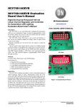
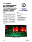
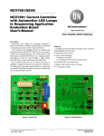
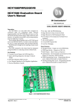
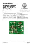
NCV7681LGEVB
NCV7681LGEVB Evaluation
Board User'sManual
Eight (8) Channel Enhanced 100 mA
Linear Current Regulator and Controller
for Automotive LED Lighting
Evaluation Board User’s Manual
www.onsemi.com
EVAL BOARD USER’S MANUAL
Description
The NCV7681L is an octal LED driver designed for automotive
LED car rear combination lamps. External programmability of the
NCV7681L allows the user to set the tail current and stop currents
using a single resistor for each function.
A one-out all-out function disable all strings when an open circuit
occurs on one string.
Systems not requiring one-out all-out have the option of using the
NCV7681A.
The two typical control inputs into the system are available through
on-board switches or through the pin connections to external controls.
The two system control inputs are the STOP and TAIL functions.
The STOP function displays a 100% duty cycle current through the
LEDs. The TAIL function displays a programmable PWM current
through the LEDs.
TAIL Mode
Features
• One Out, All Out (Latch Off) Optional Functionality
• STOP, TAIL (100% Duty Cycle, PWM) Modes
• Flexibility for
♦
♦
♦
♦
♦
External LED Connections
LED Current Programmability (RSTOP)
LED PWM Programmability (RTAIL)
STOP, TAIL External Connections
External DIAG Pin Connection
Application
The NCV7681L features the ability to drive 8 individual strings of
LEDs (reference Figure 2) with a programmed current for a DC
current for STOP mode and a PWM current for TAIL model. These are
programmed using resistors to ground on the RSTOP and RTAIL pins.
Control of the STOP and TAIL functions use an external network of
diodes with the STOP pin. LED open string reporting is reported on
the DIAG pin. The DIAG pin also serves to reset a latched off event.
System power distribution is accomplished using voltage feedback on
the top LED anode programming a set voltage in the system to allow
a split between the IC and the ballast transistor.
© Semiconductor Components Industries, LLC, 2015
October, 2015 − Rev. 0
1
STOP Mode
Figure 1. Evaluation Board Picture
Publication Order Number:
EVBUM2323/D
NCV7681LGEVB
Voltage
Regulation
Feedback
Ballast
Transistor
LED
Loads
String 2
String 1
Ballast
VP Drive
STOP/TAIL
Selection & Activation
VBAT
DIAG
RSTOP
RTAIL
Current Programming
String 4
String 5
String 6
String 7
String 8
OUT2
OUT3
OUT4
OUT5
OUT6
OUT7
OUT8
FB
STOP
Open Circuit
Reporting and Reset
String 3
OUT1
GND
NCV7681
Figure 2. Focus Demonstration
STOP
TAIL
The STOP function displays the highest system output
current at 100% duty cycle. Using the STOP switch activates
this function. The current is programmable with a resistor on
the RSTOP pin to ground. Jumper J3 provides isolation of
pin 7 of the NCV7681 allowing access to the pin for
alterative selection of output current. The range of
programmability is from 15 mA to 100 mA using the
equation:
The TAIL function displays a lower equivalent output
current in the system. This provides a lower illumination of
the LEDs. This is achieved with a varied duty cycle of the
output current. The duty cycle is programmable with
a resistor on the RTAIL pin to ground. Jumper J4 provides
isolation of pin 6 of the NCV7681L allowing access to the
pin for alternative selection of output duty cycle current.
The range of programmability is from 0% duty cycle to
100% duty cycle using the equation:
I OUT +
150
RSTOP
RTAIL + 1.8
where DC = duty cycle expressed in fractional form.
100
100
90
90
80
80
70
DUTY CYCLE (%)
IOUT OUTPUT CURRENT (mA)
where RSTOP is the resistor value.
RSTOP (DC)0.22)
60
50
40
30
20
70
60
50
40
30
20
10
0
T = 25°C
0
1
2
3
4
5
6
7
8
9
10
0
10
0
RSTOP (kW)
1
2
3
4
5
RTAIL (kW)
Figure 4. Duty Cycle vs. RTAIL
Figure 3. IOUT vs. RSTOP
www.onsemi.com
2
6
7
NCV7681LGEVB
Latch Off (“One-Out, All-Out”)
To use external LEDs,
1. Remove J14 or J18 depending on your setup
2. Replace with the Anode of your external LED
string (connect to the post on the right).
3. If needed, connect the post on the left also with the
anode of your external LED string.
4. Remove your selection of J6−J13 (OUTx,y).
5. Connect the Cathode of your external LED string
(connect to the post on the right).
To improve user aesthetics, the system design utilizes the
Latch Off function. All outputs will become latched off
when any one of the 8 outputs experiences an open circuit
condition. This is defined (at 50 mA) in the electrical
parameter “Open Circuit Detection Threshold” and has
limits between 35% and 65% of the output current. DIAG
RESET switch SW3 provides a system refresh by
temporarily grounding the DIAG pin.
DIAG
The operation of the NCV7681L evaluation board works
as a standalone presentation for the customer. Jumpers are
provided for flexibility of customer specific designs with
external LEDs and programming of the current and duty
cycle. External control points are also provided in addition
to the on-board control switches. The user must adhere to the
absolute maximum ratings when using off-board
connections.
Note the inclusion of the Open Load Disable Threshold in
the NCV7681L device. This is included to avoid false open
load detection at low supply voltages due to headroom issues
with external LEDs. Operation of LED drive current is valid
above the Output Under Voltage Lockout threshold
(VP = 4.1 V [typ]), allowing for illumination down to that
voltage, but open load detection is only valid above
VP = 7.7 V [typ].
The DIAG pin of the NCV7681L provides system
feedback for conditions:
1. Output open circuit.
2. Set Back Current Limit down 20%.
3. Thermal shutdown.
4. RSTOP Current Limit.
An LED indicator with a current setting resistor provides
illumination of these conditions. Jumper J5 provides access
to these pins for the user to use off-board.
External LEDs
The NCV7681LGEVB is compatible for use with
external LEDs.
Table 1. ABSOLUTE MAXIMUM RATINGS
Value
Unit
Supply Voltage to board (VBAT)
Rating
−40 to 40
V
STOP, TAIL
−40 to 40
V
200
mA
Output Pin Voltage (OUT1−OUT8)
−0.3 to 40
V
Output Pin Voltage (RTAIL, RSTOP)
−0.3 to 3.6
V
DIAG
−0.3 to 40
V
VSTRING
−0.3 to 40
V
Junction Temperature (NCV7681L)
−40 to 150
°C
Junction Temperature (Evaluation Board)
−40 to 105
°C
LED Current Source (OUT1−OUT8)
Stresses exceeding those listed in the Maximum Ratings table may damage the device. If any of these limits are exceeded, device functionality
should not be assumed, damage may occur and reliability may be affected.
Table 2. RECOMMENDED BOARD OPERATING CONDITIONS
Value
Rating
External Supply Voltage (VBAT)
LED Current Source
Junction Temperature (NCV7681L)
Min
Max
Unit
−
28
V
−
200
mA
−40
150
°C
Functional operation above the stresses listed in the Recommended Operating Ranges is not implied. Extended exposure to stresses beyond
the Recommended Operating Ranges limits may affect device reliability.
www.onsemi.com
3
NCV7681LGEVB
Table 3. PIN FUNCTION DESCRIPTION
Connector
Power
Pin Number
Terminal Name
Description
J1, VBAT
VBAT
Power Supply Input Voltage (14 V)
J2, GND
GND
Ground
J3
RSTOP
Programmable DC Current
J4
RTAIL
Programmable Duty Cycle
J5
DIAG
DIAG Open Drain Output and Open Circuit Reset Input
J6
J7
J8
J9
J10
J11
J12
J13
OUT1
OUT2
OUT3
OUT4
OUT5
OUT6
OUT7
OUT8
Current Outputs
J14
BALLAST IN
J15
J15
Connection to Top of the FB Resistor Network or Open Circuit
J16
J16
Connection to Short FB Pin to Ground or Open Circuit
J17
J17
Connection for Ballast Drive Gate Pin to Ballast Gate or to Ground
J18
BALLAST OUT
Connect when Using External Ballast Transistor.
Connects Drain of External Ballast Transistor to VSTRING.
Connect when Not Using External Ballast Transistor. Shorts S-D of External
Transistor.
User Interface Locations
This lists all the user options available on the evaluation
board.
Figure 5 shows all the user interface locations.
Figure 5. User Interface Locations
Black − STOP, TAIL external connections.
Grey – STOP, TAIL switches.
Dark Blue (2) – STOP programming jumper.
Red (2) – TAIL programming jumper + post.
Dark Green – VP post.
Purple (2) – VSTRING post.
Light Blue (4) – OUT1−OUT8 open circuit jumpers.
Orange − OUT1−OUT8 output posts.
Yellow – Ballast Transistor Selection (2 yellow boxes).
Light Green – DIAG RESET.
Bright Red – DIAG jumper / post.
Brown – Feedback post (FB).
www.onsemi.com
4
NCV7681LGEVB
OPERATIONAL GUIDELINES
Change the Duty Cycle
Change the duty cycle programming resistor.
Reference the TAIL section.
The material necessary to successfully use the evaluation
board is listed below.
• NCV7683 Evaluation Board
• 14 V Power Supply Capable of drive 1 A.
Latch Off
After creating an open circuit and replacing all open
circuit jumpers (OUT6−OUT8), press the DIAG RESET
switch.
Configure the Board
Typical Board Configuration with On-Board Components
1. Connect all jumpers on the board with the
exception of Jumper 18.
J15−J17 should be to the left.
2. Connect the 14 V power supply.
3. Turn on the power supply.
DIAG
The on-board LED will illuminate when DIAG reports
a fault.
Reporting can be taken off-board after removing the
DIAG jumper (J5).
Increasing the LED Current
Change the current programming resistor.
Reference the STOP section.
Use External LEDs
Reference the External LEDs section for instructions.
SCHEMATIC
2 J18 1
TAIL
J1
Vbat
Vstring
VP
1
NTD2955
U2
SW1
D25
TAIL
MRA4003
R5
1K
STOP
D26
STOP
MRA4003
J15
3
2
1
SW2
2 J14 1
J2
GND
R4
9.53K
FB
1
3
2
1
J17
J16
R8
4.99K
1
2
3
R7
1K
R1
10K
R6
10K
D27
led_diode
D22
D23
D24
led_diode
D19
led_diode
D20
led_diode
D21
led_diode
D16
led_diode
D17
led_diode
D18
led_diode
D13
led_diode
D14
led_diode
D15
led_diode
D10
led_diode
D11
led_diode
D12
2 J13 1
3
OUT1
R2 3.01K
J5
1
2
J3
1
2
J4
1
R3 1.62K
OUT1
VP
Blst
FB
STOP
OUT2
OUT3
OUT4
GND
OUT5
DIAG
OUT6
RSTOP OUT7
RTAIL OUT8
17
DIAG
2
1
2
3
4
5
6
7
8
16
15
14
13
12
11
10
9
2 J12 1
OUT2
2 J11 1
OUT3
epad
2 J10 1
OUT4
GND GND GND GND
SW3
DIAG RESET
OUT5
1
J9
2
1
J8
2
OUT6
1
J7
OUT8
Figure 6. Evaluation Board Schematic
www.onsemi.com
5
J6
led_diode
D7
D8
led_diode
D9
led_diode
led_diode
led_diode
D4
D5
D6
led_diode
led_diode
led_diode
2
OUT7
1
led_diode
D1
D2
D3
led_diode
led_diode
led_diode
2
C1
100nF
NCV7681LGEVB
BILL OF MATERIALS
Table 4. NCV7681L LATCH OFF EVALUATION BOARD BILL OF MATERIALS
Designator
Qty
Description
Value
Tolerance
Footprint
Manufacturer
Manufacturer
Part Number
Substitution
Allowed
C1
1
LED Storage
Capacitor
100 nF
10%
0805
KEMET
C0805C104K5RACTU
Yes
C2
1
Debounce
Capacitor
10 nF
10%
0805
KEMET
C0805C103K5RACTU
Yes
C3
1
Input Capacitor
0.68 mF
10%
0805
KEMET
C0805C684K5RACTU
Yes
C4
1
Loop Stabilization
Capacitor
0.22 mF
10%
0805
KEMET
C0805C224K5RACTU
Yes
D1−D24
24
Display LEDs
led_diode
−
G6SP
OSRAM
LRG6SP−CADB−1−1
Yes
D25−D26
2
Steering Diode
MRA4003
−
SMA_DIODE
ON SEMICONDUCTOR
MRA4003T3G
Yes
D27
1
DIAG Reporting
LED
led_diode
−
0805
LITE−ON INC
LTST−C171GKT
Yes
J3−J14, J18
13
Dual Jumper
Posts 100 mil
spacing
JUMPER
−
JMP
3M
961102−6404−AR
Yes
J15−J17
3
Triple Jumper
Posts 100 mil
spacing
JUMPER
−
JMP
3M
961102−6404−AR
Yes
J3−J18
16
Jumper
−
−
N/A
SULLINS
CONNECTOR
SOLUTIONS
QPC02SXGN−RC
Yes
J1
1
Banana Jack
VBAT
−
BANANA
CINCH
CONNECTIVITY
SOLUTIONS
108−0740−001
Yes
J2
1
Banana Jack
GND
−
BANANA
CINCH
CONNECTIVITY
SOLUTIONS
108−0740−001
Yes
Q2
1
DIAG Illumination
Transistor Switch
2N7002W
−
SOT23M4
ON SEMICONDUCTOR
ONC
2N7002WT1G/BKN
Yes
R1, R6
2
Logic Resistors
10 kW
1%
0805
VISHAY DALE
CRCW080510K0FKEA
Yes
R2
1
RSTOP Program
Resistor
3.01 kW
1%
0805
VISHAY DALE
CRCW08053K01FKEA
Yes
R3
1
RTAIL Program
Resistor
1.62 kW
1%
0805
VISHAY DALE
CRCW08051K62FKEA
Yes
R4
1
Vstring Program
Resistor
9.53 kW
1%
0805
VISHAY DALE
CRCW08059K53FKEA
Yes
R5
1
Gate−source
Resistor
1 kW
1%
0805
VISHAY DALE
CRCW08051K00FKEA
Yes
R7
1
Vstring Program
Resistor
1 kW
1%
0805
VISHAY DALE
CRCW08051K00FKEA
Yes
R8
1
DIAG LED
Current Setting
Resistor
4.99 kW
1%
0805
VISHAY DALE
CRCW08054K99FKEA
Yes
SW1, SW2
2
User Interface
Switches
−
−
MINITOGGLE
C & K COMPONENTS
T101MH9CBE
Yes
SW3
1
SPST−NO 0.05A
24V Tactile
Switch
−
−
6x6
TE Connectivity
Alcoswitch
1−1825910−0
Yes
TP1−TP18,
TAIL
18
Test Inputs
−
−
TP
KEYSTONE
ELECTRONICS
5010
Yes
U1
1
NCV7681L
(SOIC−16WB
epad)
−
−
16WEPAD
ON SEMICONDUCTOR
NCV7681LPWR2G
No
U2
1
NVD2955
−
−
DPAK3_SMD
ON SEMICONDUCTOR
NVD2955T4G
No
www.onsemi.com
6
NCV7681LGEVB
ON Semiconductor and the
are registered trademarks of Semiconductor Components Industries, LLC (SCILLC) or its subsidiaries in the United States and/or other countries.
SCILLC owns the rights to a number of patents, trademarks, copyrights, trade secrets, and other intellectual property. A listing of SCILLC’s product/patent coverage may be accessed
at www.onsemi.com/site/pdf/Patent−Marking.pdf. SCILLC reserves the right to make changes without further notice to any products herein. SCILLC makes no warranty, representation
or guarantee regarding the suitability of its products for any particular purpose, nor does SCILLC assume any liability arising out of the application or use of any product or circuit, and
specifically disclaims any and all liability, including without limitation special, consequential or incidental damages. “Typical” parameters which may be provided in SCILLC data sheets
and/or specifications can and do vary in different applications and actual performance may vary over time. All operating parameters, including “Typicals” must be validated for each
customer application by customer’s technical experts. SCILLC does not convey any license under its patent rights nor the rights of others. SCILLC products are not designed, intended,
or authorized for use as components in systems intended for surgical implant into the body, or other applications intended to support or sustain life, or for any other application in which
the failure of the SCILLC product could create a situation where personal injury or death may occur. Should Buyer purchase or use SCILLC products for any such unintended or
unauthorized application, Buyer shall indemnify and hold SCILLC and its officers, employees, subsidiaries, affiliates, and distributors harmless against all claims, costs, damages, and
expenses, and reasonable attorney fees arising out of, directly or indirectly, any claim of personal injury or death associated with such unintended or unauthorized use, even if such claim
alleges that SCILLC was negligent regarding the design or manufacture of the part. SCILLC is an Equal Opportunity/Affirmative Action Employer. This literature is subject to all applicable
copyright laws and is not for resale in any manner.
PUBLICATION ORDERING INFORMATION
LITERATURE FULFILLMENT:
Literature Distribution Center for ON Semiconductor
19521 E. 32nd Pkwy, Aurora, Colorado 80011 USA
Phone: 303−675−2175 or 800−344−3860 Toll Free USA/Canada
Fax: 303−675−2176 or 800−344−3867 Toll Free USA/Canada
Email: [email protected]
N. American Technical Support: 800−282−9855 Toll Free
USA/Canada
Europe, Middle East and Africa Technical Support:
Phone: 421 33 790 2910
Japan Customer Focus Center
Phone: 81−3−5817−1050
www.onsemi.com
7
ON Semiconductor Website: www.onsemi.com
Order Literature: http://www.onsemi.com/orderlit
For additional information, please contact your local
Sales Representative
EVBUM2323/D